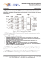
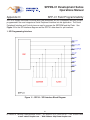
1
SPPDS-01 Development Suites
Operations Manual
For SPP-01 Platform Products
SPPDS-01 Development Suites
Operations Manual
Table of Contents
Chapter I . . . . . . . . . . . . . . . . . . . . . . . . . . . . . . . . . . . . . . . . . . . . . . . . . . . . . . . . . . . . . . . . . . . . . . . . . . . .Page
1.1. Introduction . . . . . . . . . . . . . . . . . . . . . . . . . . . . . . . . . . . . . . . . . . . . . . . . . . . . . . . . . . . . . . . . . . . . . . . . 3
1.2. Set-Up . . . . . . . . . . . . . . . . . . . . . . . . . . . . . . . . . . . . . . . . . . . . . . . . . . . . . . . . . . . . . . . . . . . . . . . . . . . 5
1.3. SPP-01 Architecture . . . . . . . . . . . . . . . . . . . . . . . . . . . . . . . . . . . . . . . . . . . . . . . . . . . . . . . . . . . . . . . . . 7
1.4. Related Documents . . . . . . . . . . . . . . . . . . . . . . . . . . . . . . . . . . . . . . . . . . . . . . . . . . . . . . . . . . . . . . . . . . 9
Chapter II
2.1. Hardware Inputs/Outputs . . . . . . . . . . . . . . . . . . . . . . . . . . . . . . . . . . . . . . . . . . . . . . . . . . . . . . . . . . . . . .10
2.2. Timing/Interrupts . . . . . . . . . . . . . . . . . . . . . . . . . . . . . . . . . . . . . . . . . . . . . . . . . . . . . . . . . . . . . . . . . . . .11
2.3. Initialization of the Serial Port 0 as an I2S Slave . . . . . . . . . . . . . . . . . . . . . . . . . . . . . . . . . . . . . . . . . . . .12
2.4. Module "init_bsp0.asm" configures McBSP0 . . . . . . . . . . . . . . . . . . . . . . . . . . . . . . . . . . . . . . . . . . . . . . .12
2.5. Initialization of Serial Port 1 for SPI Protocol . . . . . . . . . . . . . . . . . . . . . . . . . . . . . . . . . . . . . . . . . . . . . . .13
2.6. Memory Map . . . . . . . . . . . . . . . . . . . . . . . . . . . . . . . . . . . . . . . . . . . . . . . . . . . . . . . . . . . . . . . . . . . . . . .13
Chapter III
3.1. Developing of Custom Applications . . . . . . . . . . . . . . . . . . . . . . . . . . . . . . . . . . . . . . . . . . . . . . . . . . .
3.2. Creating a Code Composer Studio project (CCS) . . . . . . . . . . . . . . . . . . . . . . . . . . . . . . . . . . . . . . . .
3.3. Creating your own application . . . . . . . . . . . . . . . . . . . . . . . . . . . . . . . . . . . . . . . . . . . . . . . . . . . . . . .
3.4. Modifying BRINT0.asm . . . . . . . . . . . . . . . . . . . . . . . . . . . . . . . . . . . . . . . . . . . . . . . . . . . . . . . . . . . .
3.5. Reading the Serial Port Receive Register(s) . . . . . . . . . . . . . . . . . . . . . . . . . . . . . . . . . . . . . . . . . . . .
3.6. Writing to the Serial Port Transmit Register(s) . . . . . . . . . . . . . . . . . . . . . . . . . . . . . . . . . . . . . . . . . . .
3.7. Creating a Boot-Table . . . . . . . . . . . . . . . . . . . . . . . . . . . . . . . . . . . . . . . . . . . . . . . . . . . . . . . . . . . . .
.
.
.
.
.
.
.
.
.
.
.
.
.
.
.15
.17
.17
.19
.20
.20
.21
Appendix
A. An FIR Filter Example
B. SPP-01 Utilities . . . . .
C. Code Listings . . . . . .
D. Field Programmability
E. Terminology . . . . . . .
.
.
.
.
.
.
.
.
.
.
.22
.23
.27
.41
.46
.
.
.
.
.
.
.
.
.
.
.
.
.
.
.
.
.
.
.
.
.
.
.
.
.
.
.
.
.
.
.
.
.
.
.
.
.
.
.
.
.
.
.
.
.
.
.
.
.
.
.
.
.
.
.
.
.
.
.
.
.
.
.
.
.
.
.
.
.
.
.
.
.
.
.
.
.
.
.
.
.
.
.
.
.
.
.
.
.
.
.
.
.
.
.
.
.
.
.
.
.
.
.
.
.
.
.
.
.
.
.
.
.
.
.
.
.
.
.
.
.
.
.
.
.
.
.
.
.
.
.
.
.
.
.
.
.
.
.
.
.
.
.
.
.
.
.
.
.
.
.
.
.
.
.
.
.
.
.
.
.
.
.
.
.
.
.
.
.
.
.
.
.
.
.
.
.
.
.
.
.
.
.
.
.
.
.
.
.
.
.
.
.
.
.
.
.
.
.
.
.
.
.
.
.
.
.
.
.
.
.
.
.
.
.
.
.
.
.
.
.
.
.
.
.
.
.
.
.
.
.
.
.
.
.
.
.
.
.
.
.....
.....
.....
.....
.....
.
.
.
.
.
.
.
.
.
.
.
.
.
.
.
.
.
.
.
.
.
.
.
.
.
.
.
.
.
.
.
.
.
.
.
.
.
.
.
.
List
1.
2.
3.
4.
5.
6.
7.
8.
9.
10.
11.
12.
13.
of Figures
RS232 Cable Connection for SPPDB-01 . . . . . . . . . . . . . . . . . . . . . . . . . . . . . . . . . . . . . . . . . . . . . . . . . . 4
SPPDS-01 Development Suite Hardware Configuration . . . . . . . . . . . . . . . . . . . . . . . . . . . . . . . . . . . . . . . 5
SPP-01 Functional Block Diagram . . . . . . . . . . . . . . . . . . . . . . . . . . . . . . . . . . . . . . . . . . . . . . . . . . . . . . . 6
SPP-01 Architecture . . . . . . . . . . . . . . . . . . . . . . . . . . . . . . . . . . . . . . . . . . . . . . . . . . . . . . . . . . . . . . . . . 7
SPP-01 Inputs and Outputs . . . . . . . . . . . . . . . . . . . . . . . . . . . . . . . . . . . . . . . . . . . . . . . . . . . . . . . . . . . .10
SPP-01 DSP Interrupts to the I2S Serial Audio Format Protocol . . . . . . . . . . . . . . . . . . . . . . . . . . . . . . . . .11
Code Fragment of BRINT0.asm, Kernel Template . . . . . . . . . . . . . . . . . . . . . . . . . . . . . . . . . . . . . . . . . . .19
SPPDB-01 Hardware Configuration . . . . . . . . . . . . . . . . . . . . . . . . . . . . . . . . . . . . . . . . . . . . . . . . . . . . . .24
SPPDB-01 GUI Control Display . . . . . . . . . . . . . . . . . . . . . . . . . . . . . . . . . . . . . . . . . . . . . . . . . . . . . . . .25
Bin file display . . . . . . . . . . . . . . . . . . . . . . . . . . . . . . . . . . . . . . . . . . . . . . . . . . . . . . . . . . . . . . . . . . . . . .25
SPP-01 / SPI Interface Block Diagram . . . . . . . . . . . . . . . . . . . . . . . . . . . . . . . . . . . . . . . . . . . . . . . . . . . .41
An FIR filter Flash Memory Map Illustration . . . . . . . . . . . . . . . . . . . . . . . . . . . . . . . . . . . . . . . . . . . . . . . .44
Circuit required to provide memory access for the SPP-01 family of products . . . . . . . . . . . . . . . . . . . . . .45
List
1.
2.
3.
4.
of Tables
Key SPP-01 Hardware Components . . . . . . . . . . . . . . . . . . . . . . . . . . . . . . . . . . . . . . . . . . . . . . . . . . . . . 8
SPP-01 Hardware Component References . . . . . . . . . . . . . . . . . . . . . . . . . . . . . . . . . . . . . . . . . . . . . . . . 9
Configuration of Serial Port . . . . . . . . . . . . . . . . . . . . . . . . . . . . . . . . . . . . . . . . . . . . . . . . . . . . . . . . . . . .13
SPP-01 Kernel Core and Templates . . . . . . . . . . . . . . . . . . . . . . . . . . . . . . . . . . . . . . . . . . . . . . . . . . . . .15
25 Locust St, Haverhill, Massachusetts 01830 • Tel: 800/252-7074, 978/374-0761 • FAX: 978/521-1839
e-mail: [email protected] • Web Address: http://www.freqdev.com
SPPDS-01 Development Suites
Operations Manual
Chapter I
Introduction
This manual is for developers familiar with Texas Instruments (TI), Code Composer Studio
(CCS) and the assembly language for DSPs within the C54X family from TI. It provides enough
detail for the user to modify the templates and create calls to user-specific routines.
Frequency Devices’ Signal Processing Platform Development Suite (SPPDS-01) allows users
to develop Digital Signal Processor (DSP) software to be run on the SPP-01 dual channel signalprocessing platform. SPP-01’s are easy to use and enable the designer to take advantage of a
proven hardware platform with a flexible software kernel so products can be quickly and economically developed. The SPPDS-01 runs in CCS, TI’s powerful DSP development environment and
uses the Spectrum Digital Emulator (SDE) # XDS510PP Plus JTAG. This is the only emulator
tested!
The SPP-01 dual channel signal-processing platform combines 24 bit A/D and D/A converters, a powerful DSP, 4 megabits of flash memory and 256k bits of EEPROM, making it well suited for a broad range of audio bandwidth applications from 10 Hz to 20 kHz.
1.1 Hardware Description
The SPP-01 hardware uses a 24-bit ADC to digitize both analog input channels and transfers
the digitized data to buffers in DSP memory for processing. The processed data is then transferred to a 24-bit DAC, where it is converted back to an analog signal. The SPP-01 will operate
utilizing either normal precision or extended precision, depending on the particular requirements
of a given application. The SPPDS-01 Development Suite also provides the option of single
channel processing, which doubles the SPP-01 processing power. A JTAG interface is provided
for access to the SPP-01 platform hardware.
If desirable, multiple SPP-01 platforms can be used by taking advantage of the
MASTER/SLAVE option, which with an external driver, allows the user to sync-up several "slave"
SPP-01’s with a master.
The SPP-01 software kernel is designed for ease-of-use, allowing the end user to easily link
application-specific DSP algorithms. The kernel implements DSP initialization, ADC and DAC initialization, serial port configuration interrupts, and saves the contents of the registers, allowing
the design engineer to link the application-specific DSP software to the existing SPP-01 software
kernel. For designers who wish to insert their own software into the kernel, the SPP-01 also provides complete flexibility to pick and choose among the kernel elements.
A single precision FIR filter algorithm is included as an example of how to develop
user-specific DSP algorithms (See Appendix A and C). Using this example enables users to
quickly develop their own software.
The Signal Processing Platform Development Suite (SPPDS-01) allows users to develop
Digital Signal Processor (DSP) software to run on SPP-01 hardware.
3
25 Locust St, Haverhill, Massachusetts 01830 • Tel: 800/252-7074, 978/374-0761 • FAX: 978/521-1839
e-mail: [email protected] • Web Address: http://www.freqdev.com
SPPDS-01 Development Suites
Operations Manual
Introduction
Chapter I
The SPPDS-01 Development Suite includes:
• SPP-01 – Dual Channel Signal Processing Platform
• SPPDB-01 - Development Board Hardware for the SPP-01
• CDDS-01 – SPPDS-01 Development Software that includes example programs, utilities,
documentation and this Operations Manual.
• SPPDF-01 – FIR Filter Design Suite utilizes SPP-01 and SPPDB-01 hardware, along with
CDDF-01 software.
• CDDF-01 – Contains:
o The Filter Coefficient Generator (FCG) - A MatLabTM compatible FIR GUI linked to the
MatLabTM engine V5.3 or V6.0, and the FIR filter development object code.
o The Filter Coefficient Loader (FCL) - A tool that translates MatLabTM generated coefficient files into correct format for writing into the SPP-01 for FIR filter development.
o The SPPDF-01 Manual, data sheets, and library files.
• DB9, RS232 Cable – See Figure 1.
PROVIDED BY CUSTOMER:
• Personal Computer
• Spectrum Digital Emulator (SDE) – Model #XDS510PP w/DB25 and JTAG cables.
No other emulator has been tested.
• Code Composer Studio (CCS), - TI’s C54x specific, version 1.20 or later.
• MatLabTM Software - version V5.3 or V6.0
SIGNAL
PIN
PIN
SIGNAL
TX
RX
GND
3
2
5
3
2
5
TX
RX
GND
Figure 1 - DB9, RS232 Cable Connection for SPPDB-01
4
25 Locust St, Haverhill, Massachusetts 01830 • Tel: 800/252-7074, 978/374-0761 • FAX: 978/521-1839
e-mail: [email protected] • Web Address: http://www.freqdev.com
SPPDS-01 Development Suites
Operations Manual
Chapter I
Introduction
1.2 Set-Up
Algorithm Development is done using the SPP-01 hardware and software, TI’s, CCS and the
SDE. CCS must be installed and set up to use the SPPDS-01 Development Suite. See the
CCS manual for installation and setup of CCS and the SDE manual for installation and setup of the
emulator. The SDE must be compatible with a 1.8 volt core and 3.3 volt peripherals.
Figure 2 depicts the elements in the SPPDS-01 development environment. The SDE, in conjunction with CCS, provides access to the DSP for debugging (single stepping, use of breakpoints,
etc.). The SDE also allows you to run your software so measurements can be made to ensure that
application-specific algorithms are working as intended. The SDE is connected to the JTAG interface
on the SPP-01 board. JTAG refers to TI’s "scan-based" emulation and is a superset of the IEEE
1149.1 standard. The SDE is connected to the PC’s parallel printer port via a DB25 cable. The SPP01 hardware platform is attached to the SPPDB-01 development board, which is connected to a PC
with a DB9 cable via the RS232 interface.
DB9
Figure 2 - SPPDS-01 Development Suite Hardware Configuration
See the SPPDB-01 Development Platform datasheet for a detailed schematic. The user writes
the algorithm on a PC using TI’s, CCS. The programmer can then download this code into the SDE
through the parallel port. The SDE is also connected to the SPP-01 via the JTAG. The Algorithm
can be tested; single stepped and run in real-time. Upon successful testing of the code, the customer can then burn the code into the EEPROM and load the coefficient files into the flash memory
on the SPP-01 via the serial interface on the SPPDB-01, using the SPPDB-01 programmer software
contained on the CDDS-01.
Field programmability may be added to the SPP-01 application by building the circuit shown in
Appendix D, Figure 13. This circuit emulates the SPPDB-01 development board and permits field
loading of new EEPROM algorithms and Flash memory coefficient sets using the above mentioned
SPPDB-01 programmer software. An example of Flash memory mapping for an FIR filter is also
provided.
5
25 Locust St, Haverhill, Massachusetts 01830 • Tel: 800/252-7074, 978/374-0761 • FAX: 978/521-1839
e-mail: [email protected] • Web Address: http://www.freqdev.com
SPPDS-01 Development Suites
Operations Manual
Introduction
Chapter I
Figure 3 shows a functional block diagram of the SPP-01 depicting the flow of audio bandwidth signal from input to output. The SPP-01 data sheet details electrical, and mechanical
specifications along with a list of application-specific algorithms for those customers who desire a
turnkey solution.
Figure 3 - SPP- 01 Functional Block Diagram
SPPDS-01 software (CDDS-01) contains; core DSP assembly routines, a memory directive
command file, and templates.
The core DSP assembly routines provide:
• Initialization of the DSP - including stack pointers and relocation of the vector table.
• Initialization of the ADC and DAC - including disabling the high-pass filter, enabling calibration, and disabling the de-emphasis filter.
• Configuration - of the two serial ports and the general-purpose input/output (I/O).
• Allocation - of memory and variables.
• Linker Directive Examples - that specify how "sections" are allocated in memory.
• A Hex Utility Example - that creates a bootable table for the DSP, which can be interpreted by the SPPDB-01 or universal programmers.
The CDDS-01 software contains DSP templates. These templates include placeholders that
provide a link between the SPPDS-01 software and the application-specific software developed
by the user.
An SPPDB-01 program utility is also provided. This utility uses the RS232 interface to burn
the SPP-01 EEPROM with a bootable program and loads coefficients into Flash memory.
6
25 Locust St, Haverhill, Massachusetts 01830 • Tel: 800/252-7074, 978/374-0761 • FAX: 978/521-1839
e-mail: [email protected] • Web Address: http://www.freqdev.com
SPPDS-01 Development Suites
Operations Manual
Chapter I
Introduction
1.3 SPP-01 Architecture
A detailed block diagram of the SPP-01 hardware is shown in Figure 4. The SPP-01
hardware is built around TI’s TMS320C5402 DSP (C5402). The C5402 is a 16-bit fixed-point
processor operating at 100 MHz, which corresponds to a 10 ns CPU instruction cycle. There are
16k words of RAM on the C5402. Analog inputs and outputs for the SPP-01 hardware are provided by dual 24 bit ADCs & DACs, operating at a sampling rate of 48 kHz on each of two channels (for a total throughput of 96k samples per second). A three-wire digital output bus (I2S)
gives the user access to the C5402’s serial data output. The SPP-01 boots from a 256 kbits
EEPROM at power-up. The DSP can read pre-stored data from the 4 Mbits of onboard Flash.
Figure 4 - SPP- 01 Architecture
7
25 Locust St, Haverhill, Massachusetts 01830 • Tel: 800/252-7074, 978/374-0761 • FAX: 978/521-1839
e-mail: [email protected] • Web Address: http://www.freqdev.com
SPPDS-01 Development Suites
Operations Manual
Introduction
Chapter I
The key components of the SPP-01 hardware are listed in Table 1.
Item
DSP
EEPROM
Flash
LDO
ADC
DAC
Voltage Translator
Part Number
TMS320VC5402DSP
AT25256
AT45DB041A
TPS70151
CS5937
AD1852
SN74CBTD3384PW
Supplier
Texas Instruments
Atmel
Atmel
Texas Instruments
Cirrus Logic
Analog Devices
Texas Instruments
Table 1 - Key SPP-01 Hardware Components
An LDO voltage regulator provides the dual voltages for the DSP core and the DSP
peripherals. It also provides initial power sequencing to the DSP when power is applied to the
SPP-01 hardware. The ADC and DAC sampling frequency of 48 kHz are derived from a 12.288
MHz oscillator, which is divided by 256 within the ADC. The ADC is the master of the industry
standard I2S (Inter-IC Sound) serial audio protocol that is used to communicate between ADC,
DAC and the DSP. The DSP’s McBSP0 is the slave of this interface and is configured for the I2S
protocol. Selecting the ADC as the master of the interface minimizes jitter in the sampling times
that may occur in a DSP-master implementation.
During normal operation, the DSP boots from the serial EEPROM after power-up because
the INT3 pin is tied to the BDX1 pin. The boot loader software in the C5402 ROM loads the
user-specific DSP software into DSP RAM according to the parameter setting of the hex conversion utility (see Section 3.4 for details on the hex conversion process). Execution begins after
the software is transferred to DSP RAM.
The DSP can read pre-stored data from the Flash. The Flash is read at power-up and
again if the user input lines change state.
The SPP-01 hardware accepts two fully differential analog inputs. For the maximum 7VRMS input the signal is attenuated by 5 before going to the ADC, which allows an input of 1.4
VRMS. There are two analog outputs from the SPP-01 hardware as well as two digital outputs
that correspond to the analog input. A serial clock (SCLK) and a left/right clock (LRCK) accompany the data line. The amplitudes of the analog DAC outputs (2 VRMS) are multiplied by 3.5,
providing a default gain of 0 dB and a full-scale output of 7 VRMS.
As mentioned earlier, multiple SPP-01 platforms can be used if the MASTER/SLAVE
option is taken advantage of. The clock on the "Slave" is removed and, in their place, the clock
from the "Master" is used. This, in addition to tying all of the LRCK signals together, will sync-up
the data acquired at each SPP-01.
8
25 Locust St, Haverhill, Massachusetts 01830 • Tel: 800/252-7074, 978/374-0761 • FAX: 978/521-1839
e-mail: [email protected] • Web Address: http://www.freqdev.com
SPPDS-01 Development Suites
Operations Manual
Chapter I
Introduction
1.4 Related Documents
Table 2 below provides hardware component references that apply to the chips on the
SPP-01 and software related to CCS. TI’s books may be obtained from TI’s literature center
(800/477-8924) at no cost. Other documents are available for download at the respective manufacturer’s web sites.
TITLE
Reference
Date
Code Composer Studio Users Guide
Emulator Model XDS510PP,
Part Number 701014
(www.spectrumdigital.com)
TMS320C54x Assembly Language Tools
(www.ti.com)
TMS320C54x DSP Reference Set Vol. 5:
Enhanced Peripherals
TMS320C54x DSP Reference Set Vol. 2:
Mnemonic Instruction Set
TMS320C54x DSP Reference Set Vol. 1:
CPU and Peripherals
SPRU328B
February 2000
SPRU102D
December 1999
SPRU302
June 1999
SPRU172B
June 1998
SPRU131
April 1999
SPRS079B
October 1998,
Revised July 1999
Rev. 1432D-01/01
TMS320VC5402 Fixed Point Signal
Processor: Datasheet
ATMEL 4-megabits Serial DataFlash
(AT45DB041A) (www.atmel.com)
ATMEL SPI Serial EEPROMs (AT25256)
TPS70151 Dual-Output Low-Dropout
Voltage Regulators with Power Up
Sequencing for Split Voltage DSP Systems
Crystal 24-bit 105 dB ADC (CS5937)
(www.cirrus.com)
Analog Devices 24-bit DAC (AD1852)
(www.analog.com)
SLVS22A
Rev. 0872F-09/99
December 1999,
Rev. March 2000
DS290PP3
Apr ‘00
Rev.0
Table 2 - SPP-01 Hardware Component References
9
25 Locust St, Haverhill, Massachusetts 01830 • Tel: 800/252-7074, 978/374-0761 • FAX: 978/521-1839
e-mail: [email protected] • Web Address: http://www.freqdev.com
SPPDS-01 Development Suites
Operations Manual
Chapter II
SPP-01 Platform Description
2.1. Hardware Inputs/Outputs
Figure 5 shows the inputs and outputs on the SPP-01 platform. The differential inputs go
through a 3-pole Butterworth anti-aliasing filter that attenuates the signals by 5. The signals
have to be attenuated so the SPP-01 input range (7 VRMS) can match up with the ADC input
range (1.4 VRMS). The signals then enter the ADCs. The outputs from the DACs (up to 2 VRMS)
are fed into reconstruction filters that multiply the signals by 3.5. This is done to compensate for
the attenuation in the anti-aliasing filters and provides SPP-01 outputs of 7 VRMS. The output
signals from the SPP-01 are single-ended.
D0 – D8
D9
9–bit program select pins
Channel select pin;
Ch 1= 0, Ch 2=1
Out 1 & 2
Analog outputs
±Inputs 1&2 Differential analog inputs
± 15 V
Analog DC power In
+5V
Digital Power In
A Gnd
Analog Grounds (3)
D Gnd
Digital Grounds (2)
JTAG
JTAG port
Figure 5 - SPP-01 Inputs and Outputs
10
25 Locust St, Haverhill, Massachusetts 01830 • Tel: 800/252-7074, 978/374-0761 • FAX: 978/521-1839
e-mail: [email protected] • Web Address: http://www.freqdev.com
SPPDS-01 Development Suites
Operations Manual
Chapter II
SPP-01 Platform Description
2.2. Timing and Interrupts
A 12.288 MHz crystal provides the master clock, which is the timing reference for the
ADC. A divider in the ADC generates a left-right clock (LRCK) with a frequency of 48 kHz and a
serial clock (SCLK) with a frequency of 3.072 MHz for sampling the input signals. If this is a
"Slave" SPP-01, the master clock, SCLK and LRCK signals come from the "Master" SPP01. The ADC samples the two channels simultaneously. The 24-bit words are clocked into the
DSP on an alternating basis.
Figure 6 shows the clock and data signals that exist between the ADC, DAC and the DSP.
The SCLK, LRCK, and the serial data out lines are also available to the user via SPP-01, I/O
pins. Figure 6 also shows the interrupts generated in the DSP.
Figure 6 - DSP interrupts to I2S Serial Audio Format Protocol
There are three interrupts for each period of the LRCK.
• The BXINT0/ interrupt (the Buffered serial port Transmission INTerrupt on port number
0) is generated by the rising edge of LRCK. See Section 2.3 for the configuration of
Serial Port 0.
• The BXINT0/ interrupt service routine "tags" the samples as coming from the left. In
the single channel implementation, the samples from the second channel are ignored.
• There are two BRINT0/ interrupts (the Buffered serial port Receive INTerrupt on port
number 0) per LRCK cycle, one for each of the two channels. These interrupts, signal
the reception of the last bit of the sampled data for that sampling period. After this
interrupt, the data (either a left or a right channel sample) can be transferred from the
DSP’s data receive register to the DSP main memory.
Processing for a given channel can occur upon the reception of the last bit. When two channels are being processed, the processing must complete approximately 500 nanoseconds before the
reception of the next BRINT0/ interrupt to ensure that the data can be clocked in and out correctly.
During dual channel operation, there are approximately 9 microseconds available for processing. The Output Flag Pin (XF) on the SPP-01 (see Figure 5, Section 2.1), can be used to
observe the algorithm timing on an oscilloscope. For example, XF can be set upon entering a
channel and can be cleared upon leaving. These processing durations can be compared to the
LRCK, which is also an output on the SPP-01. A dual channel example is described in
Appendix A and C. The DSP "template" is brint0/ .asm.
11
25 Locust St, Haverhill, Massachusetts 01830 • Tel: 800/252-7074, 978/374-0761 • FAX: 978/521-1839
e-mail: [email protected] • Web Address: http://www.freqdev.com
SPPDS-01 Development Suites
Operations Manual
Chapter II
SPP-01 Platform Description
If only a single channel is needed and processing can be completed in one 9-microsecond period, then the application program should be set up as a two-channel system where only
one channel is processed. This allows the left or the right channel to be used in single channel
mode.
For single channel applications requiring greater than 9-microseconds of processing time,
the extended processing template must be used. The extended processing template doubles the
available processing time to 18 microseconds. To do this, the left channel uses the processing
normally allocated to the right channel. Since each DAC channel normally expects a digital word
every 10.8 microseconds (see Figure 6, Section 2.2), the processing must be modified, using
the single channel template.
The template executes the following; upon the rising edge of LRCK, the BXINT0/ is triggered. bxint0/.asm sets the "right-channel-next" flag FALSE to indicate the next receive interrupt
will be the result of the last bit of the left channel clocking in. When the BRINT0/ interrupt occurs,
the left channel data is read. Left channel processing continues with interrupts enabled so that
the processing can continue through the next interrupt (which will correspond to the last bit of the
right channel being clocked in). Upon completion, the data is sent to the transmit register.
2.3. Initialization of the Serial Port 0 as an I2S Slave
The Serial Port 0 is dedicated to communicating with the ADC and DAC. This port is configured as the slave in an I2S protocol, which uses four digital lines to exchange data between
the ADC, DAC and DSP. The ADC provides a SCLK for clocking the sampled data into the DSP.
This same clock is used to send the processed data into the DAC. The LRCK, also generated
by the ADC, provides the interrupts to the DSP for distinguishing between the two channels. The
third signal going from the ADC to the DSP is the data line, which contains the digital word sampled in the ADC. The fourth line is the digital word sent from the DSP to the DAC after processing.
2.4. Module "init_bsp0.asm" configures McBSP0
Seven DSP registers related to McBSP0 are configured so that the port operates as an
I2S slave compatible with the ADC and DAC. Those registers are:
•
Serial port control register 1
•
Serial port control register 2
•
Receive control register 1
•
Receive control register 2
•
Transmit control register 1
•
Transmit control register 2
•
Pin control register
The port is set up as a dual phase frame where a phase corresponds to a channel of the
analog input. Although the port is capable of multiple words per frame, the ADC only sends out a
single word per frame. Each word is 32 bits. Note that the ADC only sends out 24 bits. The
extraneous 8 bits are zero, and the DAC only accepts the first 24-bits in each word.
12
25 Locust St, Haverhill, Massachusetts 01830 • Tel: 800/252-7074, 978/374-0761 • FAX: 978/521-1839
e-mail: [email protected] • Web Address: http://www.freqdev.com
SPPDS-01 Development Suites
Operations Manual
Chapter II
SPP-01 Platform Description
Table 3 lists the bits that are different than the default settings. See TI’s, SPRU302,
(Table 2, Section 1.4) the reference volume that describes the enhanced features of the McBSP0,
for a description of the default settings.
Register
Acronym
SPCR10
SPCR10
RCR20
RCR20
RCR20
RCR20
XCR10
XCR20
XCR20
XCR20
PCR0
PCR0
Name of bit
or bits and value
RJUST=10b
RINTM=10b
RPHASE=1
RWDLEN2=101b
RFIG=1
RDATDLY=01b
XWDELN1=101b
XPHASE=1
XWDELN1=101b
XDATDLY=01b
CLKXP=1
CLKRP=1
Description
The bits are left justified in the data receive register
The DSP will be interrupted on each new frame sync.
Dual-phase frame
32 bit word
Frame syncs after the first are ignored
1 bit data delay after frame sync.
32 bit word
Dual-phase frame
32 bit word
1 bit data delay after frame sync.
Tx data sampled on rising edge
Rx data sampled on rising edge
Table 3 - Configuration of Serial Port
The last digit in the register acronym indicates serial port 0. Note: These only apply to
McBSP0. There is another set for McBSP1.
2.5. Initialization of Serial Port 1 for SPI protocol
McBSP1 is configured to operate in the Serial Peripheral Interface (SPI) mode. The SPI
protocol is a synchronous data link that has a master and several slaves. On the SPP-01, the
DSP is the master, and the EEPROM, Flash, ADC, and DAC control registers are slaves. The
link to the ADC control register is used to disable the high-pass filters and enable calibration.
The link to the DAC control register is used to setup the sampling rate, software mute, deemphasis, and other functions. The DSP selects these slaves through chip select pins.
2.6. Memory Map
The memory map defines the placement in DSP memory (i.e., DSP RAM) of the following:
•
Text (the DSP code)
•
Variables
o
Input data samples
o
Output data samples
o
Filter coefficients (or other constants)
o
Scratch pad
o
Stack
13
25 Locust St, Haverhill, Massachusetts 01830 • Tel: 800/252-7074, 978/374-0761 • FAX: 978/521-1839
e-mail: [email protected] • Web Address: http://www.freqdev.com
SPPDS-01 Development Suites
Operations Manual
Chapter II
SPP-01 Platform Description
The memory map is defined in Appendix C example file link.cmd. This file includes
assembler directives.
The 5402 scratch pad is located from 0x60 to 0x7F, and is never used by the kernel.
However, the enclosed FIR example program, does utilize the following scratch pad locations
0x61, 0x62, 0x63, 0x64 and 0x65.
The stack is located from 0x3fe0 to the end of memory 0x3fff. Although this 32 word stack
is large enough for most applications, the user can make it larger by modifying " .usect
"stack",1Fh,15" in main.asm and "stack : load = 0x3fe0 PAGE 1" in link.cmd.
The interrupt vector table is placed at locations 0x80 to 0xff. The FIR example code is
started at 0x100 and can extend to 0x17ff, which are 5.8k words of program space. The kernel
uses 0.34k words of this space, so there are 5.5k words of space available for user-specific
code. For each channel, there are 4k words of space available for input data and coefficients.
See link.cmd for detail.
14
25 Locust St, Haverhill, Massachusetts 01830 • Tel: 800/252-7074, 978/374-0761 • FAX: 978/521-1839
e-mail: [email protected] • Web Address: http://www.freqdev.com
SPPDS-01 Development Suites
Operations Manual
Chapter III
SPP-01 Custom Applications
3.1. Developing Custom Applications
The SPP-01 kernel is designed to handle all of the following tasks: initializing the DSP,
enabling it, bringing data in, and sending data out. This includes the two serial ports for booting,
reading flash, and communicating with the ADC and DAC. Table 4 shows the files classified into
2 categories. The modules used in initialization are files that need not be modified and are
referred to as SPP Kernel Core. Vectors.asm and bxint0.asm are not used at initialization but
are included in the core since they do not need to be modified.
The Kernel Templates will need to be
applications. The key routine is brint0.asm.
SPP Kernel Core
ad1852.asm
cs5397.asm
flash.asm
bxint0.asm
Vectors.asm
init_bsp0.asm
init_bsp1.asm
wppr.asm
modified by the user in the development of custom
SPP Kernel Templates
Main.asm
brint0.asm
link.cmd
TABLE 4 - Kernel Core and Templates
This routine is responsible for the exchange of digital data between the ADC, the DAC and
the DSP. Specifically, this routine reads data in the DSP receive registers (samples from the
ADC) and writes data to the DSP transmit registers (samples to the DAC). It is from this routine
that user-specific algorithms are called.
The SPP-01 kernel comes with the following files:
a. Source files of the kernel’s core routines:
c:\SPP01 Kernel Core
c:\SPP01 Kernel Core\ad1852.asm
c:\SPP01 Kernel Core\cs5397.asm
c:\SPP01 Kernel Core\bxint0.asm
c:\SPP01 Kernel Core\flash.asm
c:\SPP01 Kernel Core\init_bsp0.asm
c:\SPP01 Kernel Core\init_bsp1.asm
c:\SPP01 Kernel Core\vectors.asm
c:\SPP01 Kernel Core\wppr.asm
The user will modify these templates:
c:\SPP01 Kernel Templates\
c:\SPP01 Kernel Templates\main.asm
c:\SPP01 Kernel Templates\brint0.asm
c:\SPP01 Kernel Templates\link.cmd
15
25 Locust St, Haverhill, Massachusetts 01830 • Tel: 800/252-7074, 978/374-0761 • FAX: 978/521-1839
e-mail: [email protected] • Web Address: http://www.freqdev.com
SPPDS-01 Development Suites
Operations Manual
SPP-01 Custom Applications
Chapter III
b. FIR filter examples are included in the SPPDS-01 Development Suite, See Appendix A
and C. These files implement a low-pass FIR filter on channel one, and band-pass filter
on channel two. This directory, when combined with the files of the core, forms a CCS
project. Among these files, coeff.bin is a binary file that includes the low-pass and bandpass filter coefficients. The reason this example is included is to give the user familiarity
with developing SPP-01 applications.
c:\SPP01 Kernel Example App Specific Files\
c:\SPP01 Kernel Example App Specific Files\main.asm
c:\SPP01 Kernel Example App Specific Files\fir.asm
c:\SPP01 Kernel Example App Specific Files\coeff.bin
c. An executable file created by the FIR example is also included. This is useful when starting out to ensure that the hardware (SPP-01 and SDE emulator) and the software are in
working order. The program takes the left channel data and processes it through a lowpass digital filter with a –0.01dB cut-off of approximately 3000 Hz, and a –96dB stop of
approximately 3700Hz. The right channel data is processed through a band-pass filter
with a center frequency of approximately 3050Hz and bandwidth of 100Hz. The left and
right inputs can be tied to the same signal source and the outputs can be observed on a
scope.
c:\SPP01 Kernel Example Executable\
c:\SPP01 Kernel Example Executable\Kernel_example.out
d. These files include all the source and command files for the memory map. These files can
be copied into your user directory to form the basis for creating a CCS Project. This
directory is provided to help the user become familiar with creating CCS projects.
c:\SPP01 Kernel Example\
c:\SPP01 Kernel Example\bxint0.asm
c:\SPP01 Kernel Example\brint0l.asm
c:\SPP01 Kernel Example\init_bsp0.asm
c:\SPP01 Kernel Example\init_bsp1.asm
c:\SPP01 Kernel Example\fir.asm
c:\SPP01 Kernel Example\flash.asm
c:\SPP01 Kernel Example\ad1852.asm
c:\SPP01 Kernel Example\main.asm
c:\SPP01 Kernel Example\cs5397.asm
c:\SPP01 Kernel Example\vectors.asm
c:\SPP01 Kernel Example\link.cmd
c:\SPP01 Kernel Example\wppr.asm
c:\SPP01 Kernel Example\kernel_example.mak
16
25 Locust St, Haverhill, Massachusetts 01830 • Tel: 800/252-7074, 978/374-0761 • FAX: 978/521-1839
e-mail: [email protected] • Web Address: http://www.freqdev.com
SPPDS-01 Development Suites
Operations Manual
Chapter III
SPP-01 Custom Applications
3.2. Creating a Code Composer Studio (CCS) Project
The SPP-01 kernel was developed using TI’s CCS and the SPPDS-01 Development
Suite. Before creating a project, make sure CCS has been installed. Also make sure the emulator software has been installed.
A. Connect the emulator to the PC and the JTAG connector on the SPP-01.
B. Connect power (both 5 volts and +/-15 volts) to the SPP-01 by connecting them to the
SPPDB-01 development board. (See Figure 2, Section 1.2)
C. Power up the SDE emulator and the SPPDB-01.
Optionally, a signal generator can be connected to the SPP-01 analog inputs through the
BNCs on the SPPDB-01 development board. A scope may be connected to the SPP-01 analog
and/or digital outputs or the clock signals.
Assuming that CCS was installed and configured correctly, start CCS. If the CCS window
does not come up, recheck the configuration in the CCS setup utility or contact TI’s Technical
Support.
3.3. Creating Your Own Application:
It is assumed that all user specific applications will be written in 54x assembly language.
The steps in creating user specific applications include:
A. Write a C54x assembly language algorithm (suitable for calling by the kernel – see the
section on brint0/ .asm).
B. Modify the brint0/ .asm template so that it calls the user specific algorithm.
C. Write an initialization routine (which will probably be called from main.asm), which is
unique or required for the user-specific algorithm. (Optional)
D. Modify the memory map (link.cmd). (Optional)
E. Create a CCS project based on the user specific routines and the SPP01 core routines.
F. Debug the user specific algorithm.
17
25 Locust St, Haverhill, Massachusetts 01830 • Tel: 800/252-7074, 978/374-0761 • FAX: 978/521-1839
e-mail: [email protected] • Web Address: http://www.freqdev.com
SPPDS-01 Development Suites
Operations Manual
SPP-01 Custom Applications
Chapter III
Although this should be familiar to 54x developers, the steps involved in creating a user specific application around the SPP-01 core are outlined below. This should only be done after it
has been determined that CCS is communicating properly with the SPP-01.
A. From windows create a new directory for your application.
B. Copy the following into this newly created directory:
a. All files in the SPP-01 Kernel Core
b. main.asm from the SPP Kernel Templates
c. brint0.asm
d. Open CCS
a. Create a new project and save in the newly created directory.
b. Add the following files to the project:
i. All the files in the new project (including the link.cmd file).
ii. The application-specific source file(s).
c. In the "build option":
i. Insert "start" for the code entry point.
ii. Make sure the "-c" option is NOT included in the linker build options.
C. Edit
a. main.asm (to include any calls to initialization routines).
b. brint0 (to insert calls to the application-specific routines).
c. link.cmd (to make any necessary modifications to the memory map).
D. Develop user specific algorithm.
E. Build the project.
F. Load the executable file.
G. Run the application.
18
25 Locust St, Haverhill, Massachusetts 01830 • Tel: 800/252-7074, 978/374-0761 • FAX: 978/521-1839
e-mail: [email protected] • Web Address: http://www.freqdev.com
SPPDS-01 Development Suites
Operations Manual
Chapter III
SPP-01 Custom Applications
3.4. Modifying brint0/ .asm
BRINT0/ is the routine that needs to be modified, so it calls the user-specific algorithms
(main.asm may need to be modified as well). The basic structure for each channel is readprocess-write. Figure 7 shows a code fragment of brint0.asm. Note that the program flow is to
either the left or right channel based on a test condition of the top of the routine. See Section
2.2 for a description of the time and flow of these routines. Three lines of code are highlighted
and they need to be changed to reflect the name of the user specific module.
.ref
brint0
firSGL,TapsNum_1
stm
stm
ldm
ldm
#0, 0x38
#0100000000000001b, 0x39
0x20,a
;read most significant word from drr20
0x21,b
;read least significant word from drr10
cmpm
nop
bc
@ar7, 0x01
;determine which channel is active n
right_channel,tc
;----------------------------Left channel--------------------------------------left_channel mvdm
@COF_L_INDEX,ar4
;get pointers
mvdm
@DAT_L_INDEX,ar5
st
#324,@TapsNum_1
stm
#325,bk
;set circular buffer size
stm
#1, ar0
stl
a, *ar5+0%
;save new data to buffer
call
firSGL
;run algorithm
mvmd
mvmd
stm
dst
stm
rete
ar5,@DAT_L_INDEX
ar4,@COF_L_INDEX
#22h,ar1
b, *ar1
0x1, ar7
;update pointers
;send data out through McBSP0
;-----------------------right channel------------------------------------------right_channel mvdm
@COF_R_INDEX,ar4
;get pointers
mvdm
@DAT_R_INDEX,ar5
st
#324, @TapsNum_1
stm
#325,bk
;set circular buffer size
stm
#1, ar0
st
a, *ar5+0%
;save new data to buffer
call firSGL
mvmd
mvmd
stm
dst
stm
rete
;run algorithm
ar5,@DAT_R_INDEX
ar4,@COF_R_INDEX
#22h,ar1
b, *ar1
0x0, ar7
;updates pointers
;send data out through McBSP0
Figure 7 - Code Fragment of brint0.asm, Kernel Template
19
25 Locust St, Haverhill, Massachusetts 01830 • Tel: 800/252-7074, 978/374-0761 • FAX: 978/521-1839
e-mail: [email protected] • Web Address: http://www.freqdev.com
SPPDS-01 Development Suites
Operations Manual
SPP-01 Custom Applications
Chapter III
3.5. Reading the Serial Port Receive Register(s)
On the C5402, the McBSP0 receive registers are at memory location 0x20 and 0x21. Two 16-bit
locations are needed so that words up to 32 bits can be clocked into the device. Two different
methods can be used to read data that has arrived from the ADC.
3.5.1. Normal Precision
For processing in normal precision (16 bit words) use the following 54x instructions:
ld 0x20, a
ld 0x21, b
These load the 16 most significant bits into the least significant bits of the "a" accumulator.
The least significant 8 bits from the conversion are placed in "b" accumulator and are not
used. See example Figure 7.
3.5.2. Extended Precision
If extended precision processing is required, then the above two instructions should be
replaced with:
ld *(0x20),16,a
or *(0x21), a
which places the entire 24 bit sample into the "a" accumulator, left justified. The instructions should be replaced in both the left and the right channels, if extended precision is
required in both channels. Note: there is no requirement that the left and right channels be processed with the same precision.
3.6. Writing the Serial Port Transmit Register(s)
For writing data to the DAC use:
dst b, *ar1
where "ar1" must be pointing to the McBSP0 "tx" register (i.e., memory location 0x22). Note that
this instruction writes 32 bits into the registers (i.e., 0x22 and 0x23) as required for transmission
to the DAC. For single precision use, the 16 bits should be in the high portion of the accumulator.
20
25 Locust St, Haverhill, Massachusetts 01830 • Tel: 800/252-7074, 978/374-0761 • FAX: 978/521-1839
e-mail: [email protected] • Web Address: http://www.freqdev.com
SPPDS-01 Development Suites
Operations Manual
Chapter III
SPP-01 Custom Applications
3.7. Creating a Boot Table
The following "ascii" file (or a modified version of it) should be used in conjunction with CCS’s
hex conversion utility to generate a file that is compatible with the EEPROM on the SPP-01.
The hex command, executed from DOS is:
hex500 fn.cmd
where "fn" is the filename of the command file (an example is below). Note that the input COFF
filename and the output filename will need to be changed to be compatible with the names of the
user specific application. Also, the entry point must be changed if it is altered in the 54x code.
/* --------------------------------------------------------------------------*/
/* file:
hex.cmd
*/
/* Author: FDI Engineering
*/
/* Project: SPP-01 Kernel
*/
/* Date:
8/21/02
*/
/* ---------------------------------------------------------------------- */
/* Usage: hex500 hex.cmd
*/
/* ----------------------------------------------------------------------- */
/* Copyright 2002, Frequency Devices, Inc.
*/
/* ---------------------------------------------------------------------- */
kernel_example.out
/* input COFF file name
*/
/*
*/
-i
/* Intel MCS-86 Object format
*/
-e 100h
/* Entry point
*/
-boot
/* Bootload all sections in the input file */
-bootorg SERIAL
/* Boot from serial device
*/
-memwidth 8
/* EEPRROM width is 8 bits
*/
/*
*/
-o kernel_example.hex
/* Output file name
*/
/* ------------------------ end of file hex.cmd ----------------------*/
21
25 Locust St, Haverhill, Massachusetts 01830 • Tel: 800/252-7074, 978/374-0761 • FAX: 978/521-1839
e-mail: [email protected] • Web Address: http://www.freqdev.com
SPPDS-01 Development Suites
Operations Manual
FIR Filter Example
Appendix A
Appendix A describes the creation of a user specific application. Two FIR filters are implemented using normal precision. Two channels are used to demonstrate the SPP-01 programming
flexibility. A low-pass filter is implemented in the left channel and a band-pass filter is implemented in the right channel.
After developing this project and creating an executable file, the file should be loaded into the
SPP-01. Signals can be input into the left (1) and right (2) channels and the outputs can be
observed on the left and right outputs. The left channel should exhibit a cut-off at about 3000 Hz
and the right channel should operate in a band-pass filter mode.
The coefficients for these two FIR filters are included in a binary file coeff.bin. To use this
FIR example, the user must download this coefficient file to the Flash memory on the SPP-01 by
using the SPPDB-01 program utility on the CDDS-01, CDRom and described in Appendix B1.
1. From Windows, create a directory for the new application.
2. Copy the following into this newly created directory:
• All files in the SPP-01 Kernel Core
• All the SPP-01 Kernel "Example Application Specific Files" (Normally at this step the
files from the templates would be copied into the directory and then modified. The modification of
the templates has already been done in this example).
3. Open CCS
4. Create a new project and save in the newly created directory.
5. Add the following files to the project:
• All the files in the new project (including the link.cmd file)
• The application-specific source file(s)
• In the "build option":
6. Insert "start" for the code entry point
7. Make sure the "-c" option is NOT included in the linker build options
8. Edit (this step can be bypassed since it was already done):
• main.asm (to include any calls to initialization routines).
• brint0.asm (to insert calls to the application-specific routines).
• link.cmd to make any necessary modifications to the memory map.
9. Develop user specific algorithm (this had been done and is represented in the file fir.asm).
10. Build the project
11. Load the executable file (For operation of the SPPDB-01 program utility, see Appendix B1).
12. Run the application.
See below for a listing of the user-specific files. They include:
File
main.asm
link.cmd
fir.asm
brint0.asm
Comment
Modified to call init_FIR
Memory map
Initialize pointers, etc for use and implement a normal precision FIR algorithm
Modified to call firSGL
22
25 Locust St, Haverhill, Massachusetts 01830 • Tel: 800/252-7074, 978/374-0761 • FAX: 978/521-1839
e-mail: [email protected] • Web Address: http://www.freqdev.com
SPPDS-01 Development Suites
Operations Manual
Appendix B
SPP-01 Utilities
Two utilities for the SPP-01 are described below:
• One is the SPPDB-01 Program Utility software on the CDDS-01, CDRom which is used to
download files from a computer to the EEPROM or FLASH on the SPP-01,
• The second is the SPPDF-01 FIR filter design suite. The user can easily design and
implement FIR digital filters using MatLabTM for the SPP-01 via the SPPDF-01 software
interface on CDDF-01.
B.1 - SPPDB-01 Program Utility
SPPDB-01 program utility on the CDDS-01, CDRom is used together with the SPPDB-01 development board to program the EEPROM and Flash memory on the SPP-01.
B.1.1 - Introduction
The SPPDB-01 Programming Software is a part of the SPPDS-01 Development Suite and is found
on the CDDS-01, CDRom. This programming utility allows the user to burn executable files into the
SPP-01’s EEPROM and/or load coefficient files into its Flash memory via an RS232 interface on the
SPPDB-01 development board.
The SPP-01 EEPROM executable files contain; a kernel integrated with an algorithm for the DSP
program, along with booting and initialization instructions for the SPP-01. Upon power-up, the SPP01 EEPROM file is read and loaded into the DSP’s RAM memory. All executable files must be in
HEX format before programming the EEPROM using the SPPDB-01 program utility software. Files
can be converted to HEX format by using the HEX utility contained in the CCS Development Suite.
The next step in the SPP-01 booting sequence is reading the addressed coefficient files in Flash
Memory into the SPP-01 DSP. Whenever the SPP-01 address lines change state, a different set of
coefficients is read, altering how the algorithm (program) affects the signal processing.
Before using the SPPDB-01 program utility, it is assumed that correctly generated and tested (successfully emulated) code exists and has been converted into the appropriate file format.
B.1.2 - SPPDB-01 Program Utility installation
(1)
Place the CDDS-01 CD in the PC, CD Rom drive.
(2)
Select "Run" in the Windows Start-Up menu.
(3)
Click browse and select the appropriate drive letter.
(4)
Choose and open the SPPDB-01 folder, then select the setup file
(5)
CLICK "Open", then CLICK “OK”.
(6)
Follow the instructions on the display to complete the installation. The program should now
be listed under the Programs Menu.
23
25 Locust St, Haverhill, Massachusetts 01830 • Tel: 800/252-7074, 978/374-0761 • FAX: 978/521-1839
e-mail: [email protected] • Web Address: http://www.freqdev.com
SPPDS-01 Development Suites
Operations Manual
SPP-01 Utilities
Appendix B
B.1.3 - Initialization and GUI description
With PC, RS232 connection and the SPPDB-01 hardware set-up as shown in Figure 8, launch
the SPPDB-01 software from the program menu. The GUI Control Display appears in Figure 9.
Figure 8 - SPPDB-01 Hardware Configuration
24
25 Locust St, Haverhill, Massachusetts 01830 • Tel: 800/252-7074, 978/374-0761 • FAX: 978/521-1839
e-mail: [email protected] • Web Address: http://www.freqdev.com
SPPDS-01 Development Suites
Operations Manual
Appendix B
SPP-01 Utilities
3
1
4
2
5
6
Figure 9 - SPPDB-01 GUI Control Display
Description of Controls
(1) Comport Switch selects between COM1 and COM2. Setting depends upon which
Comport the SPPDB-01’s RS232, DB9 cable is connected to.
(2) Target Switch selects between programming the Flash memory coefficients or the
EEPROM with an executable file.
(3) Start Page controls the page number at which the Flash memory programming begins.
(4) To Select A File press the blue button to select a HEX or BIN file for programming.
Figure 10 - Bin File Display will appear as below.
Figure 10 - Bin File Display
(5) The Program Button begins programming of the EEPROM or the Flash with the previously selected file. The process can take 1 to 3 minutes, after which an indication of
successful programming is provided "Programming OK"
(6) The Quit Button exits the SPPDB-01 program.
To execute the program, the SPP-01 must be rebooted by removing and re-applying power.
25
25 Locust St, Haverhill, Massachusetts 01830 • Tel: 800/252-7074, 978/374-0761 • FAX: 978/521-1839
e-mail: [email protected] • Web Address: http://www.freqdev.com
SPPDS-01 Development Suites
Operations Manual
Appendix B
SPP-01 Utilities
B.1.4 - EEPROM Programming Example Converts the SPP-01 into an FIR filter
Follow the steps below to program the EEPROM with the example HEX file, sppdf-01.hex.
This file is included with the SPPDB-01 software on the CDDS-01, CDRom.
(1)
(2)
(3)
(4)
(5)
(6)
(7)
(8)
(9)
(10)
Start the SPPDB-01 software.
Use the Comport Switch to select the proper Comport (COM1 or COM2), depending upon
which pc comport the RS232-DB9 cable is plugged into.
Choose the EEPROM target.
Press the blue button on the Select A File window to select the HEX file indicated below.
Select sppdf-01.hex. This file is located on CDDS-01 in the Samples folder, which is in the
folder for the SPPDB-01 Programmer software. After entering the selected file CLICK on the
load button in the selection window.
Press the Program button, then formatting, programming, and verification will proceed for
about 2-3 minutes.
When verification is completed, a message will appear that says "Programming OK!"
Press the Quit button to exit the program.
Turn the power to the SPPDB-01 "OFF and ON" to re-boot the SPP-01 with the new EEPROM data. The SPP-01 will now be running the new code just programmed onto the EEPROM.
In this case, using the sppdf-01.hex file, the SPP-01 now has the appropriate boot kernel to
accept coefficients created in MatLabTM utilizing the SPPDF-01 FIR utilities contained on the
CDDF-01, CD.
B.2 - SPPDF-01
The SPPDF-01 is an FIR digital filter design and implementation suite designed to be used in
conjunction with MatLabTM V 5.3 or V 6.0. The software, on the CDDF-01 CD is divided into two
parts:
1. The Filter Coefficients Generator (FCG) Software provides tools for the generation of sets
of coefficients for single or multiple filters over a predefined bandwidth. The software provides data to produce a signal representation in the frequency domain. It is designed to
allow the user to add or modify frequency selective types of FIR filters, such as, lowpass, high-pass, band-pass, and band-stop filters.
2. The Filter Coefficients Loader (FCL) Software provides the mechanisms to perform the
following functions: interfacing, loading, communicating, translating, and formatting. The
software is a communication-translation-programming interface that loads single or multiple sets of coefficients for different filter types into an SPP-01 using an SPPDB-01 development board.
NOTE:
SPPDF.HEX is a file provided on the CDDS-01 CD in the SPPDB-01 program
folder. This file represents an FIR filter algorithm program used with the SPPDF-01 FIR filter
development suite. The SPPDF.HEX file can be programmed or "written" into the SPP-01
EEPROM by the SPPDB-01 program utility, so the SPPDS-01 user can use the FIR filter as
in the SPPDF-01FIR Filter Development Suite using the MatLabTM utilities. See program
example in Appendix section B.1.4.
NOTE:
Because the SPPDF-01 FIR Filter Development Suite may be purchased as a stand
alone item, the full operating manual and operating software for the SPPDF-01 is
contained on the enclosed CDDF-01 CDRom.
26
25 Locust St, Haverhill, Massachusetts 01830 • Tel: 800/252-7074, 978/374-0761 • FAX: 978/521-1839
e-mail: [email protected] • Web Address: http://www.freqdev.com
SPPDS-01 Development Suites
Operations Manual
Appendix C
; File:
SPP-01 Code Listings
main.asm
; Author:
FDI Engineering
; Objective:
Main routine for SPP-01 Kernel
; REVISION:
8/20/02
;------------------------------------------------------------------------------; Copyright 2002, Frequency Devices, Inc.
;------------------------------------------------------------------------------.mmregs
.def
main
.ref
init_bsp0,init_bsp1
.ref
init_ADC,init_DAC,init_FIR
TOS
BOS
usect
usect
main:
sect
ssbx
stm
stm
stm
stm
stm
"stack",1Fh,15 ;define the stack to reside at location
"stack",1h
;
"START"
intm
#0x0FFFF, ifr
#BOS, sp
;5432109876543210
#0000000010100000b,pmst
;000000001|| |
;
0| |
;
1|
;
0
#0x0ff, 0x03c
;76543210
#01011101b, 0x3d
rpt
nop
#8000
call
cal
init_bsp1
init_bsp0
stm
rpt
nop
#0x9F,0x3d
#200
call
cal
init_ADC
init_DAC
cal
init_FIR
stm
stm
#0xffff, ifr
#0x0030, imr
stm
#0,ar7
; disable all interrupts
; clear IFR flag
; set stack point to Bottom Of Stack
;
;IPTR, relocate vector to 0x0080
;MP/MC='0', on-chip ROM addressable
;OVLY='1',prog and data memory overlap
;DROM='0',on-chip ROM not mapped to data
;config HPI8 as output PINs
;HD0: Flash /CS
;HD1: DAC /RST
;HD2: ADC /CS
;HD3: DAC /CS
;HD4: not used
;HD5: SPI /WP
;HD6: ADC_DAC_CDIN buffer control
;HD7: ADC_SDATA1 buffer control
;time delay
;make ADC out of reset
set current channel to left
rsbx
ovm
ssbx
sxm
ssbx
ffrct
rsbx
intm
loop
nop
wait forever
nop
b
loop
.end
/* -----------------end of main.asm---------------------*/
27
25 Locust St, Haverhill, Massachusetts 01830 • Tel: 800/252-7074, 978/374-0761 • FAX: 978/521-1839
e-mail: [email protected] • Web Address: http://www.freqdev.com
SPPDS-01 Development Suites
Operations Manual
SPP-01 Code Listings
Appendix C
File:
link.cmd
*/
/* Author:
FDI Engineering
/* Project:
SPP01 - Kernel
/* Objective: linker cmd file for spp01
/* REVISION: 8/21/02
/**********************************************************
/* Copyright 2002, Frequency Devices, Inc.
/**********************************************************
*/
*/
*/
*/
*/
*/
*/
-m Kernel_example.map /* creat an output map */
-o Kernel_example.out
/* name the COFF output file */
/********************************************************** */
/*
specify the memory configurations
*/
/********************************************************** */
MEMORY
{
/* program space */
PAGE 0: DARAM1 (RWIX): o=00080h l=00080h
/* for interrupt vect*/
DARAM2 (RWIX): o=00100h l=03f80h
/* 0100h-1fffh DARAM (8K) */
/* data space */
PAGE 1: SCRATCH (RW) : o=00060h l=00020h
/* Scratch-Pad RAM */
DARAM3 (RWIX): o=0080h l=03f80h
/* On-Chip DARAM (8K)*/
}
/********************************************************** */
/*
specify the output sections
*/
/********************************************************** */
SECTIONS
{
.vectors
START
.text
BUF_L
BUF_R
COF_L
COF_R
stack
:
:
:
:
:
:
:
:
load
load
load
load
load
load
load
load
=
=
=
=
=
=
=
=
DARAM1 PAGE 0
DARAM2 PAGE 0
DARAM2 PAGE 0
0x1800 PAGE 1
0x2000 PAGE 1
0x2800 PAGE 1
0x3000 PAGE 1
0x3fe0 PAGE 1
}
/* -----------------end of link.cmd ---------------------*/
28
25 Locust St, Haverhill, Massachusetts 01830 • Tel: 800/252-7074, 978/374-0761 • FAX: 978/521-1839
e-mail: [email protected] • Web Address: http://www.freqdev.com
SPPDS-01 Development Suites
Operations Manual
Appendix C
; File:
SPP-01 Code Listings
AD1852.asm
-
; Author:
FDI Engineering
; Project:
SPP-01 Kernel
; Purpose :
Write 32bit data to AD1852 control register for SPP-01 ; Revision:
8/20/02
;---------------------------------------------------------------------------------------; Copyright 2002 by Frequency Devices, Inc.
;---------------------------------------------------------------------------------------;------------------------------------------------------------------------------; Input Register: A
; Used Register: B
;------------------------------------------------------------------------------.mmregs
.def init_DAC
.ref wppr
;------------------------------------------------------------------------------; Initialize AD1852 DAC
;------------------------------------------------------------------------------init_DAC
;109876543210
ld
#000000000001b,a
call
WriteDAC
-
;constrol reg
rpt
nop
#10
ld
call
;5432109876543210
#1111111111111100b,a ;volume left
WriteDAC
rpt
nop
#10
ld
call
;5432109876543210
#1111111111111110b,a ;volume right
WriteDAC
ret
;------------------------------------------------------------------------------; Write 32-bit data to AD1852 DAC control register
;------------------------------------------------------------------------------WriteDAC
ld
and
stl
0x3d,b
#0x0f7, b
b, 0x3d
;/CS=0
call
wppr
;Write 32bit data via SPI
ld
or
stl
0x3d,b
#0x08, b
b, 0x3d
;/CS=1
ret
.end
/* -----------------end of AD1852.asm ---------------------*/
29
25 Locust St, Haverhill, Massachusetts 01830 • Tel: 800/252-7074, 978/374-0761 • FAX: 978/521-1839
e-mail: [email protected] • Web Address: http://www.freqdev.com
SPPDS-01 Development Suites
Operations Manual
SPP-01 Code Listings
Appendix C
; File:
CS5397.asm
-
; Author: FDI Engineering
; Project: SPP-01 Ker
; Purpose : Write 32bit data to CS5397 ADC register for SPP-01 ; Revision: 8/20/02
;------------------------------------------------------------------------------------; Copyright 2002 by Frequency Devices, Inc.
;------------------------------------------------------------------------------------;------------------------------------------------------------------------------; Input Register: A
; Used Register: B
;------------------------------------------------------------------------------.mmregs
.def init_ADC
.ref wppr
;------------------------------------------------------------------------------; Initialize CS5397 ADC
;------------------------------------------------------------------------------;set FSTART and GND CAL
init_ADC
ld
#0001h,16,a
or
#0C000h, a
call WriteADC
rpt #200
nop
;set LRCK to 48KHZ from 96Khz, set DFS as I2S
ld
#0002h,16,a
or
#4a00h, a
call
WriteADC
Delay1
;set FSTART and GND CAL
ld
#4000,a
nop
rpt
#65500
nop
sub
#1,a
nop
bc
Delay1,aneq
rpt
nop
#200
ld
or
call
#0001h,16,a
#0000h, a
WriteADC
rpt
nop
#200
ld
or
call
#0002h,16,a
#0a00h, a
WriteADC
ret
30
25 Locust St, Haverhill, Massachusetts 01830 • Tel: 800/252-7074, 978/374-0761 • FAX: 978/521-1839
e-mail: [email protected] • Web Address: http://www.freqdev.com
SPPDS-01 Development Suites
Operations Manual
Appendix C
SPP-01 Code Listings
;------------------------------------------------------------------------------; Write 32-bit data to CS5397 ADC control register
;------------------------------------------------------------------------------WriteADC
ld
0x3d,b
;/CS=0
and #0x0fffb, b
stl
b, 0x3d
call wppr
;write 32bit data via SPI
ld
0x3d,b
;/CS=1
or
#0x0004, b
stl b, 0x3d
ret
.end
;-----------------------------------end of file CS5397.asm------------------; File:
bxint0.asm
-
; Author:
FDI Engineeri
; Project:
SPP01 - Kernel
; REVISION: 8/20/02
;-----------------------------------------------------------------------------; Copyright 2002, Frequency Devices, Inc.
;-----------------------------------------------------------------------------.def bxint0
bxint0
stm
#0x0, ar7
rete
;--------------------- end of file bxint0.asm ---------------------------------
; File:
brint0.asm
-
; Author:
FDI Engineering
; Project:
SPP-01 Kernel
; Objective(s):
McBSP0 receive interrupr service routine ; REVISION:
8/20/02
;------------------------------------------------------------------------------; Copyright 2002, Frequency Devices, Inc.
;------------------------------------------------------------------------------.mmregs
brint0
.def
.ref
.ref
brint0
DAT_L_INDEX,DAT_R_INDEX,COF_L_INDEX,COF_R_INDEX
firSGL,TapsNum_1
stm
stm
#0, 0x38
#0100000000000001b, 0x39
ldm
ldm
0x20,a
0x21,b
cmpm @ar7, 0x01
nop
bc
right_channel,tc
nop
;----------------------------Left
left_channel
mvdm
mvdm
st
stm
;read most significant word from drr20
;read least significant word from drr10
;determine which channel is active now
channel--------------------------------------@COF_L_INDEX,ar4 ;get pointers
@DAT_L_INDEX,ar5
#324,@TapsNum_1
#325,bk
;set circular buffer size
31
25 Locust St, Haverhill, Massachusetts 01830 • Tel: 800/252-7074, 978/374-0761 • FAX: 978/521-1839
e-mail: [email protected] • Web Address: http://www.freqdev.com
SPPDS-01 Development Suites
Operations Manual
SPP-01 Code Listings
Appendix C
stm
stl
#1, ar0
a, *ar5+0%
;save new data to buffer
call
firSGL
;run algorithm
mvmd
mvmd
ar5,@DAT_L_INDEX ;update points
ar4,@COF_L_INDEX
stm
dst
stm
rete
#22h,ar1
b, *ar1
0x1, ar7
;send data out through McBSP0
;-----------------------right channel------------------------------------------right_channel
mvdm @COF_R_INDEX,ar4 ;get pointers
mvdm
@DAT_R_INDEX,ar5
st
#324, @TapsNum_1
stm
#325,bk
;set circular buffer size
stm
#1, ar0
stl
a, *ar5+0%
;save new data to buffer
call
firSGL
;run algorithm
mvmd
mvmd
ar5,@DAT_R_INDEX ;updates pointers
ar4,@COF_R_INDEX
stm
dst
stm
rete
#22h,ar1
b, *ar1
0x0, ar7
;send data out through McBSP0
.end
; File:
fir.asm
-
; Author:
FDI Engineering
; Project:
SPP01 - Kernel
; Objective:
Implements a single precision(16-bit data and 16-bit coeficients ;
FIR filter
; REVISION:
8/20/02
;------------------------------------------------------------------------------------------------------; Copyright 2000, Frequency Devices, Inc.
;------------------------------------------------------------------------------------------------------.mmregs
.def firSGL,init_FIR
.def COEF_L,COEF_R,DATA_L,DATA_R
.def DAT_L_INDEX,DAT_R_INDEX,COF_L_INDEX,COF_R_INDEX
.def TapsNum_1
.ref ReadFLASH
DAT_L_INDEX
.set 60h
COF_L_INDEX
.set 61h
DAT_R_INDEX .set 62h
COF_R_INDEX .set 63h
TapsNum_1
.set 64h
.sect "BUF_L"
DATA_L
.space 2048*16
;reserved for left channel data in
.sect "BUF_R"
DATA_R
.space 2048*16
;reserved for right channel data in
.sect "COF_L"
COEF_L
.space 2048*16
;coefficients table for left channel
.sect "COF_R"
COEF_R
.space 2048*16
;coefficients table for right channel
.text
32
25 Locust St, Haverhill, Massachusetts 01830 • Tel: 800/252-7074, 978/374-0761 • FAX: 978/521-1839
e-mail: [email protected] • Web Address: http://www.freqdev.com
SPPDS-01 Development Suites
Operations Manual
Appendix C
SPP-01 Code Listings
;------------------------------------------------------------------------------;read FIR filter coefficients to internal RAM from flash
;------------------------------------------------------------------------------init_FIR
;left channel is a 325 taps lowpass fir filter which coefficients
;are stored in flash memory from page 300 to 302
stm
#300, ar2
; ar2->first page
stm
#2, ar3
; ar3=(TotalPage-1)
stm
#COEF_L, ar6
; first location of coef memory
call
ReadFLASH
;right channel is a 325 taps bandpass fir filter which coefficients
;are stored in flash memory from page 303 to 305
stm
#303, ar2
; ar2->first page
stm
#2, ar3
; ar3=(TotalPage-1)
stm
#COEF_R, ar6
; first location of coef memory
call
ReadFLASH
stm
stm
stm
stm
#COEF_L, @COF_L_INDEX
#DATA_L, @DAT_L_INDEX
#COEF_R, @COF_R_INDEX
#DATA_R, @DAT_R_INDEX
;initialize pointers for left
;channel (i.e. channel one)
;initialize pointers for right
;channel (i.e. channel two)
ret
;------------------------------------------------------------------------------; firSGL :single precision fir
; Regs used : ar4,ar5,b,ar0,TapsNum_1
;------------------------------------------------------------------------------.asg
AR5, FIR_BUF_P ;point to the oldest sample
.asg
AR4, FIR_COF_P
firSGL
LD
RPT
MAC
#0000h, B
@TapsNum_1
*FIR_BUF_P+0%, *FIR_COF_P+0%, B
RET
end
; File:
FLASH.asm
-
; Author:
FDI Engineering
; Project:
SPP01 - Kernel
; Objective(s):
Provides the DSP capability to read AT45DB041A DataFlash
;
in SPP01 platform
; REVISION:
8/20/02
;-----------------------------------------------------------------------------; Copyright 2000 Frequency Devices, Inc.
;------------------------------------------------------------------------------
-
.mmregs
;----------------------------------------------------------------------------;
Instruction sets for AT45DB041A---SPI mode
;----------------------------------------------------------------------------; Read Commands
CAREAD
.set 0E8h
; Continuous Array Read (total chip read)
MPREAD
.set 0D2h
; Main memory page read
B1READ
.set 0D4h
; Buffur1 read
B2READ
.set 0D6h
; Buffer2 read
SRREAD
.set 0D7h
; Status Register Read
; Program and Erase Commands
B1WRITE
.set 84h
; Buffer1 write
B2WRITE
.set 87h
; Buffer2 write
33
25 Locust St, Haverhill, Massachusetts 01830 • Tel: 800/252-7074, 978/374-0761 • FAX: 978/521-1839
e-mail: [email protected] • Web Address: http://www.freqdev.com
SPPDS-01 Development Suites
Operations Manual
SPP-01 Code Listings
Appendix C
B1TOMPINERS
B2TOMPINERS
B1TOMPNOERS
B2TOMPNOERS
PAGEERASE
BLOCKERASE
MMPPBYB1
MMPPBYB2
.set
.set
.set
.set
.set
.set
.set
.set
;Additional Commands
MPTOB1TR
.set
MPTOB2TR
.set
MPTOB1CMP
.set
MPTOB2CMP
.set
PRWBYB1
.set
PRWBYB2
.set
83h
86h
88h
89h
81h
50h
82h
85h
;
;
;
;
;
;
;
;
Buffer1 to Main page Prog with erase
Buffer2 to Main page Prog with erase
Buffer1 to main page prog without erase
Buffer2 to main page prog without erase
page Erase
Block erase
Main Memory Page Prog through Buffer1
Main Memory Page Prog through Buffer2
53h
55h
60h
61h
58h
59h
; Main memory Page to Buffer1 transfer
; Main memory Page to Buffer2 transfer
; Main memory page to Buffer1 Compare
; Main memory page to Buffer2 Compare
; Auto Page Rewrite through Buffer1
; Auto Page Rewrite through Buffer2
;---------------------------------------------------------------------------------------------------;Note: after calling this subroutine, the father routine must store intm,ovm ;
and sxm bit if necessory
;Reg used: ar2---first page in FLASH
;
ar3---(Total Page - 1 )
;
ar6---first location of destination memory
;
a,b
;
ar4,ar5,a,b
in SPIRW
;
;-----------------------------------------------------------------------------------------------------.def ReadFLASH,SPIRW
PAGE_LEN
.set 66
.asg ar2, PAGE_P
; ar2->first page
.asg ar3, TOTAL_PAGE_P ; ar3=(TotalPage-1)
.asg ar6, COEFTBL_P
; first location of coef memory
ReadFLASH
ld
#MPREAD, 16, a
sftl a, 8
ldm PAGE_P, b
sftl
b,9
or
b, a
; a = 0x 00 00d2 0000
; a = 0x 00 d200 0000
; or opcode and page address (result in 'a')
call LowCS
nop
nop
nop
call
ld
call
SPIRW
#0, a
SPIRW
; 1. Send out opcode and address, no need to store
; put zero into 'a' as don't care transmission
; 2. Send 32 don't care bits, no need to store
stm #(PAGE_LEN-1), brc; 66 32 bit words corresponds to one page
nop
rptb
nop
ld
call
nop
nop
dst
nop
nop
LoopB-1
#0x0, a
SPIRW
; a dummy write
; 3. Send 32 don't care bits, but keep data that was
a, *COEFTBL_P+
LoopB
;make /CS=1 , end of reading
34
25 Locust St, Haverhill, Massachusetts 01830 • Tel: 800/252-7074, 978/374-0761 • FAX: 978/521-1839
e-mail: [email protected] • Web Address: http://www.freqdev.com
SPPDS-01 Development Suites
Operations Manual
Appendix C
SPP-01 Code Listings
call HighCS
nop
nop
ldm PAGE_P, b
add #1, b
stlm b, PAGE_P
; PAGE_P points to next page
banz ReadFLASH, *TOTAL_PAGE_Pnop
ret
;-----------------------------------------------------------------------------;
Make the HD0-CS low to select DataFlash
;-----------------------------------------------------------------------------LowCS
ld
0x3d,b
; b=(GPIOSR) Hd0--HD7
and #0x0fffe, b
stl
b, 0x3d
; make HD0=0, /CS=0
ret
;-----------------------------------------------------------------------------;
Make the HD0-CS low to select DataFlash
;-----------------------------------------------------------------------------HighCS
ld
0x3d,b
; b=(GPIOSR) Hd0--HD7
or
#0x0001, b
stl
b, 0x3d
; make HD0=0, /CS=0
ret
;-----------------------------------------------------------------------------;
McBSP Sub-bank addressed registers
;-----------------------------------------------------------------------------DRR21
.set 40h
DRR11
.set 41h
DXR21
.set 42h
DXR11
.set 43h
SPSA1
.set 48h
;McBSP1 subbank address
SPSD1
.set 49h
;McBSP1 subbank data
SPCR1
SPCR2
RCR1
RCR2
XCR1
XCR2
SRGR1
SRGR2
PCR
.set
.set
.set
.set
.set
.set
.set
.set
.set
00h
01h
02h
03h
04h
05h
06h
07h
0Eh
;Serial Port Control Register 1.
;Serial Port Control Register 2.
;Recieve Control Register 1.
;Recieve Control Register 2.
;Transmit Control Register 1.
;Transmit Control Register 2.
;Sample Rate Generator Register 1.
;Sample Rate Generator Register 2.
;Pin Control Register.
;-----------------------------------------------------------------------------;
MACRO for SPI flash operation using c5402's McBSP1;-----------------------------------------------------------------------------; reg used : A,AR4,AR5
; entry : A : 8-bit op-code + 16-bit address + 8-bit data
; output: A :stores byte from flash 8-bit LSB is valid
; note : The caller must make up the 32-bit frame by himself before ;
calling this routine
;-----------------------------------------------------------------------------SPIRW
STM #SPSA1, AR4
STM #DXR21, AR5
35
25 Locust St, Haverhill, Massachusetts 01830 • Tel: 800/252-7074, 978/374-0761 • FAX: 978/521-1839
e-mail: [email protected] • Web Address: http://www.freqdev.com
SPPDS-01 Development Suites
Operations Manual
SPP-01 Code Listings
Appendix C
DST
ST
BIT
BCD
BITF
A, *AR5
#SPCR2, *AR4+
*AR4,14
; test XRDY
$, NTC
*AR4,2h
MAR *AR4MAR *AR5MAR *AR5-
;AR4->SPSA1
;AR5->DRR11
;AR5->DRR21
ST
BIT
BCD
BITF
#SPCR1, *AR4+
*AR4, 14
$, NTC
;test RRDY
*AR4,2h
LD
OR
*AR5+,16, A
*AR5,A
;rx word to A
ret
.end
; File:
INIT_BSP0.asm
-
; Author:
FDI Engineering
; Project:
SPP-01 Kernel
; Objective:
Configure McBSP0 of c5402 as Slave of an I2S protocol;
communicating with CS5397 ADC and AD1852 DAC ; REVISION:
8/20/02
;------------------------------------------------------------------------------; Copyright 2002 by Frequency Devices, Inc.
;------------------------------------------------------------------------------;------------------------------------------------------------------------------;Uage
: .ref init_bsp0
;
call init_bsp0
;regs used:
none
;------------------------------------------------------------------------------.mmregs
.def init_bsp0
init_bsp0:
stm #0x0, 0x38
stm #0100000000100000b,0x39
stm #0x1, 0x38
stm #0x0, 0x39
stm #2,0x38
stm #0000000010100000b,0x39
stm #3,0x38
stm #1000000010100101b,0x39
stm #4,0x38
stm #0000000010100000b,0x39
stm
stm
stm
stm
#5,0x38
#1000000010100101b,0x39
#0x0E ,0x38
#0x03, 0x39
stm #1, 0x38
stm #0000000000100001b, 0x39
rpt #100
;wait for serial port ready
36
25 Locust St, Haverhill, Massachusetts 01830 • Tel: 800/252-7074, 978/374-0761 • FAX: 978/521-1839
e-mail: [email protected] • Web Address: http://www.freqdev.com
SPPDS-01 Development Suites
Operations Manual
Appendix C
SPP-01 Code Listings
nop
ret
;------------------------- end of file init_bsp0.asm ----------------------------
; File:
init_bsp1.asm
-
; Author:
FDI Engineering
; Project:
SPP-01 Kernel
; Objective:
Initialize the McBSP1 of c5402 as a SPI master which can ;
communicate with EEPROM and FLASH in SPI mode0. ; REVISION:
8/20/02
;------------------------------------------------------------------------------; Copyright 2002 by Frequency Devices, Inc.
;------------------------------------------------------------------------------;------------------------------------------------------------------------------; Usage
: .ref init_bsp1
;
call init_bsp1
; Regs used :
ar4
;------------------------------------------------------------------------------;------------------------------------------------------------------------------;
McBSP Sub-bank addressed registers
;------------------------------------------------------------------------------SPSA1
SPSD1
SPCR1_sub
SPCR2_sub
RCR1_sub
RCR2_sub
XCR1_sub
XCR2_sub
SRGR1_sub
SRGR2_sub
PCR_sub
.set
.set
.set
.set
.set
.set
.set
.set
.set
.set
.set
48h
49h
00h
01h
02h
03h
04h
05h
06h
07h
0Eh
;McBSP1 Address register
;McBSP1 Data Register
;Serial Port Control Register 1.
;Serial Port Control Register 2.
;Recieve Control Register 1.
;Recieve Control Register 2.
;Transmit Control Register 1.
;Transmit Control Register 2.
;Sample Rate Generator Register 1.
;Sample Rate Generator Register 2.
;Pin Control Register.
;------------------------------------------------------------------------------.def init_bsp1
SCLKDIV
.set 199
;the divisor for the serial clock rate of SPI
init_bsp1
stm #SPSA1, ar4
;ar4 point to SPSA1
st #SPCR1_sub, *AR4+ ;Sub-bank Address (SPSA) = SPCR1.
st #1800h, *AR4;Reset xmiter and enable clkstp=11b.
st
st
#XCR1_sub, *AR4+ ;Set Sub-bank Address to XCR1.
#0A0h, *AR4;Select 32-bit packets for xmit.
st
st
#XCR2_sub, *AR4+ ;Set Sub-bank Address to XCR2.
#1h, *AR4;Select 1bit delay for xmit.
st
st
st
st
#SPCR2_sub, *AR4+ ;Set Sub-bank Address to SPCR2.
#0200h, *AR4;Reset rcvr and clk gen, FREE=1 .#1
;above should be tx, not rcvr
#RCR1_sub, *AR4+ ;Set Sub-bank Address to RCR1.
#0A0h, *AR4;Select 32-bit packets for rcv.
st
st
#RCR2_sub, *AR4+ ;Set Sub-bank Address to RCR2.
#1h, *AR4;Select 1bit delay for rcv.
st
#SRGR1_sub, *AR4+ ;Set Sub-bank Address to SRGR1.
37
25 Locust St, Haverhill, Massachusetts 01830 • Tel: 800/252-7074, 978/374-0761 • FAX: 978/521-1839
e-mail: [email protected] • Web Address: http://www.freqdev.com
SPPDS-01 Development Suites
Operations Manual
SPP-01 Code Listings
Appendix C
st
#SCLKDIV, *AR4-
st
st
#SRGR2_sub, *AR4+ ;Set Sub-bank Address to SRGR2.
#2000h, *AR4;Configure frames.
rpt #(2*SCLKDIV-18)
nop
st
st
;Delay for 2bit clocks
;2*(SCLKDIV-9) cycles
#SPCR2_sub, *AR4+ ;Set Sub-bank Address to SPCR2.
#0240h, *AR4;Take clk gen out of reset. #1.5
rpt #(2*SCLKDIV-18)
nop
st
st
;bit rate=sysclk/(accuA+1).
;Delay for 2bit clocks
;2*(SCLKDIV-9) cycles
#PCR_sub, *AR4+ ;Set Sub-bank Address to PCR.
#0A0Dh, *AR4;CLKXM=1/FSXM=1/CLKXP=0/CLKRP=1
;FSRP=FSXP=1.
#2
rpt #(2*SCLKDIV-18) ;Delay for 2bit clocks
nop
;2*(SCLKDIV-9) cycles
st
st
st
st
#SPCR1_sub, *AR4+ ;Set Sub-bank Address to SPCR1.
#01801h, *AR4- ;Enable McBSP transmitter.
#5
#SPCR2_sub, *AR4+ ;Set Sub-bank Address to SPCR2.
#0241h, *AR4;Enable McBSP reciever.
#5
rpt #(2*SCLKDIV-18) ;Delay for 2bit clocks
nop
;2*(SCLKDIV-9) cycles
ret
;------------------------- end of file init_bsp1.asm ---------------------------
; File:
VECTORS.asm
-
; Author:
FDI Engineering
; Project:
SPP-01 Kernel
; Purpose :
C5402 interrupt vectors table SPP-01
; Revision:
8/20/02
;------------------------------------------------------------------------------; Copyright 2002 by Frequency Devices, Inc.
;------------------------------------------------------------------------------.title "c5402 vectors table, Page6-47"
.mmregs
.ref main,brint0,bxint0
.sect
RS
NMI
SINT
INT0
".vectors"
BD main
NOP
NOP
RETE
NOP
NOP
NOP
.space 16*4*14
RETE
NOP
NOP
-
;GOTO main
;NMI
@0004h
;sint17
@0008h
;sint30
@003fh
;exter int0 @0040h
NOP
38
25 Locust St, Haverhill, Massachusetts 01830 • Tel: 800/252-7074, 978/374-0761 • FAX: 978/521-1839
e-mail: [email protected] • Web Address: http://www.freqdev.com
SPPDS-01 Development Suites
Operations Manual
Appendix C
INT1
INT2
TINT
BRINT0
BXINT0
BRINT2
BXINT2
INT3
HPINT
BRINT1
BXINT1
DMAC4
DMAC5
RETE
NOP
NOP
NOP
RETE
NOP
NOP
NOP
RETE
NOP
NOP
NOP
BD brint0
NOP
NOP
BD bxint0
NOP
NOP
RETE
NOP
NOP
NOP
RETE
NOP
NOP
NOP
RETE
NOP
NOP
NOP
RETE
NOP
NOP
NOP
RETE
NOP
NOP
NOP
RETE
NOP
NOP
NOP
RETE
NOP
NOP
NOP
RETE
NOP
NOP
NOP
* reserved
SPP-01 Code Listings
;exter int1 @0044h
;exter int2 @0048h
;timer
@004ch
;McBSP0 rx
@0050h
;McBSP0 tx
@0054h
;McBSP2 rx // DMAC0 @0058h
;McBSP2 tx // DMAC1 @005ch
;exter int3 @0060h
;HPI int
@0064h
;McBSP1 rx // DMAC2 @0068h
;McBSP2 tx // DMAC3 @006ch
;DMA channel 4 @0070h
;DMA channel 5 @0074h
@0078h to @007fh
.space 16*4*2
.END
39
25 Locust St, Haverhill, Massachusetts 01830 • Tel: 800/252-7074, 978/374-0761 • FAX: 978/521-1839
e-mail: [email protected] • Web Address: http://www.freqdev.com
SPPDS-01 Development Suites
Operations Manual
SPP-01 Code Listings
Appendix C
; File:
wppr.asm (Write Poll Poll Read)
-
; Author: FDI Engineering
; Project: SPP01 - Kernel
; Objective:Write 32-bit out through McBSP0 (SPI) to ADC,DAC,EEPROM and FLASH ; REVISION: 8/20/02
;------------------------------------------------------------------------------; Copyright 2002 by Frequency Devices, Inc.
;------------------------------------------------------------------------------;------------------------------------------------------------------------------; Registers used:
;
; A - The data to be written/read is passed/returned in accu A.; AR2 - Temp, local storage.
; AR3 - Address to perform operation on is passed here. ; AR4 - Must point to serial port sub-bank address reg (SPSA). ; AR5 - Must point to data transmit register2 (DXR2x).
;------------------------------------------------------------------------------;------------------------------------------------------------------------------; McBSP Sub-bank addressed registers
;------------------------------------------------------------------------------SPCR1_sub
SPCR2_sub
RCR1_sub
RCR2_sub
XCR1_sub
XCR2_sub
SRGR1_sub
SRGR2_sub
PCR_sub
.set
.set
.set
.set
.set
.set
.set
.set
.set
00h
01h
02h
03h
04h
05h
06h
07h
0Eh
;Serial Port Control Register 1.
;Serial Port Control Register 2.
;Recieve Control Register 1.
;Recieve Control Register 2.
;Transmit Control Register 1.
;Transmit Control Register 2.
;Sample Rate Generator Register 1.
;Sample Rate Generator Register 2.
;Pin Control Register.
DRR21
DRR11
DXR21
DXR11
SPSA1
SPSD1
.set
.set
.set
.set
.set
.set
40H
41H
42h
43h
48H
49H
; Data Receive Register 2
; Data Receive Register 1
; McBSP1 Data Transmit Register 2
; McBSP1 Data Transmit Register 1
; Serial Port 1 Sub-bank Address Register
; Serial Port 1 Sub-bank Data Register
wppr
.def
stm
stm
wppr
#DXR21,ar5
#SPSA1,ar4
dst
a,*ar5
; send out 32 bit word
st
bit *AR4, #14
bcd $, ntc
Bitf *AR4, #02h
mar
stm
st
bit
bcd
bitf
ld
ld
#SPCR2_sub, *AR4+ ; Set Sub-bank Address to SPCR2.
; TC=XRDY, for first poll.
; Loop for polling.
; Poll XRDY.
*AR4; AR4->SPSA
#0x40,ar5
#SPCR1_sub, *AR4+ ; SPSA->SPCR1, AR4->SPSD.
*AR4, #14
; TC=RRDY, for first poll.
$, ntc
; Loop for polling.
*AR4, #02h
; Poll RRDY
*AR5+, A
; Get received word
*ar5,b
; get remaining 16 bit word
ret
; Return
;------------------------- end of file wppr.asm -------------------------------
40
25 Locust St, Haverhill, Massachusetts 01830 • Tel: 800/252-7074, 978/374-0761 • FAX: 978/521-1839
e-mail: [email protected] • Web Address: http://www.freqdev.com
SPPDS-01 Development Suites
Operations Manual
Appendix D
SPP-01 Field Programmability
SPP-01’s contain on-board EEPROM and Flash memories, are SPI compatible and may be field
programmed if the user integrates a Serial Peripheral Interface into his application. The Serial
Peripheral Interface and Control pins are used to program the EEPROM and the Flash. See
Figure 11 for the SPI interface diagram and the SPP-01 data sheet for pin locations.
1. SPI Programming Interface
Figure 11 - SPP-01 / SPI Interface Block Diagram
41
25 Locust St, Haverhill, Massachusetts 01830 • Tel: 800/252-7074, 978/374-0761 • FAX: 978/521-1839
e-mail: [email protected] • Web Address: http://www.freqdev.com
SPPDS-01 Development Suites
Operations Manual
SPP-01 Field Programmability
Appendix D
2. SPI Pin Descriptions
There are a total of 7 signal pins used for in-system or field programming. All signals require
3.3V volts. The DGND should be connected to Programmer’s ground. DGND represents the
digital ground of SPP-01.
EMU1/OFF: When set low, all output drivers of the DSP become high-impedance. When the
DSP is disconnected from the EEPROM and Flash, an external processor may then access both
memories without conflict. During in-system programming, the EMU1/OFF pin must be set
low.
SPI_CS_FLASH: Chip select Signal for the Flash, Set Low when programming Flash.
SPI_CS_EEPROM: Chip select signal for the EEPROM, Set Low when programming EEPROM.
SPI_SO: Serial data output from the memory. Shared by the EEPROM and the Flash.
SPI_SI: Serial data input to the memory. Shared by the EEPROM and the Flash.
SPI_CLK: SPI Clock input to the memory. Shared by the EEPROM and the Flash.
SPI_/WP: Write Protect: Shared by the EEPROM and Flash. When set low, all write operations
are invalid. During programming, this signal must be set high.
3. Timing Issues
To program the EEPROM, follow these steps:
a)
EMU1/OFF = 0;
//Disable the DSP
SPI_/WP
= 1;
//Disable write protect
SPI_CS_FLASH = 1;
//The Flash is not selected
SPI_CS_EEPROM = 0;
//The EEPROM is selected
b)
ProgramEEPROM();
//please refer to the AT25256 Datasheet from
ATMEL for detailed information
c)
SPI_/WP = 0;
EMU1/OFF = 1;
//enable write protect
//enable the DSP
To program the Flash, please follow these
d)
EMU1/OFF = 0;
SPI_/WP
= 1;
SPI_CS_EEPROM = 1;
SPI_CS_FLASH = 0;
steps:
//Disable the DSP
//Disable write protect
//The EEPROM is not selected
//The Flash is selected
e)
ProgramFlash();
//please refer to the AT45DB041A Datasheet from
ATMEL for detailed information
f)
SPI_/WP = 0;
EMU1/OFF = 1;
//enable write protect
//enable the DSP
42
25 Locust St, Haverhill, Massachusetts 01830 • Tel: 800/252-7074, 978/374-0761 • FAX: 978/521-1839
e-mail: [email protected] • Web Address: http://www.freqdev.com
SPPDS-01 Development Suites
Operations Manual
Appendix D
SPP-01 Field Programmability
4. Memory Map Illustration for a Programmable FIR Filter
The SPPDF-01 Filter Development Suite software, resides on the CDDF-01 CD. This software
provides utilties that use the MatLabTM engine to create and load coefficients into a dual channel,
double precision FIR filter programmed into an SPP-01 (FIR sppdf.hex program, file on CDDS01). The coefficient memory addresses are mapped for the Flash memory by the FIR algorithm.
The FIR program resides in the EEPROM and coefficients loaded into the Flash, control the frequency response of the FIR filter. Each channel can have its own unique coefficients. The DSP
reads a 32-bit coefficient set from Flash memory for each channel according to the user’s selection. The maximum number of taps is 300. Any type of FIR filter, such as low-pass, band-pass,
multi-step, can be implemented with the DSP algorithm. This section gives some guidelines for
those users who may want to use the SPP-01 FIR filter program example (EEPROM) but change
the filter coefficients in the Flash.
See ATMEL AT25256 EEPROM and AT45DB041A Flash data sheet for further details.
The AT45DB041A Flash memory is organized into 2048 pages, each with 264 bytes. In the FIR
filter example (Appendix A and C), each filter coefficient set occupies 3 pages, regardless of the
number of taps required for the filters, so the Flash memory can theoretically accommodate up to
682 filters. The coefficient of the first filter are stored in pages 0 to 2, and the coefficients of the
second filter are stored in pages 3 to 5, and so on.
The linear phase FIR filters for the SPPDM-01 are designed to ensure that the filter coefficients
are odd or even symmetric. For example, with a filter of N taps, the coefficients set is c(n),
where n is from 0 to N-1. If c(0) is equal to c(N-1), then this is even-symmetric. If c(0) is equal
to minus c(N-1), then this filter is odd-symmetric. Also, N can be odd or even. If N is even, only
the first half of the coefficients, i.e. from c(0) to c(N/2-1) need to be programmed into appropriate
pages in the Flash memory. If N is odd, the coefficients from c(0) to c([(N+1)/2]-1) must be programmed into the Flash memory.
See the FIR programmed SPP-01 Flash memory map Figure 13.
The half filter coefficients are followed by a number of zeros and a message word. The sum of
taps, zeros and message word must be 198. Assuming N is 278, then N/2 is 139 and the number
of zeros is 198-139-1=58.
All coefficients, zeros, and the message word are 32-bit Q31 format words and are stored in the
Flash in Motorola format. This means the MSB is the lower address, while the LSB is the higher
address.
A Message Word gives the DSP some information about the filter such as the number of taps
and odd or even symmetric. Bit 31 to bit 16 and bit 13 to bit 9 are zeros, and bit 8 to bit 0 represents the number of taps. If the number of taps is even, set bit 15 to 0, otherwise to 1; If the
coefficients are even symmetric, set bit 14 to 0, otherwise to 1.
43
25 Locust St, Haverhill, Massachusetts 01830 • Tel: 800/252-7074, 978/374-0761 • FAX: 978/521-1839
e-mail: [email protected] • Web Address: http://www.freqdev.com
SPPDS-01 Development Suites
Operations Manual
Appendix D
SPP-01 Field Programmability
For example; Figure 13 shows the Flash memory mapping of an FIR filter with 268 taps. It is
designed, evenly symmetrical with floating-point coefficients. Because of the even number of
taps and even symmetric, both ET and ES are set to 0 in the message word. The number of
taps, 268, equals the binary number 100001100. Put this binary word into the message word bit
locations from bit 8 to bit 0. Next convert the floating-point coefficients into Q31 integer format.
Assume this filter is number 3, then the start page on the flash memory for the coefficients is
page 9. Now program the page 9, 10 and 11 with the first half coefficients, zeros and the message word. Each Q31 format coefficient has 32 bits, while the flash is organized as 8-bit bytes.
The coefficients must be divided into 4 bytes, with the MSB programmed into the lower address
on the Flash.
Page 9
Filter 0
Filter 1
C(0)
Byte 0
C(1)
Byte 1
Q23-Q16
Byte 2
Q15-Q8
Byte 3
Q7-Q0
FIlter 2
Filter 3
Q31-Q24
C(2) to C(65)
Filter 4
Page 10
C(66)
C(67)
Filter 5 to 680
Page 11
C(132)
C(133)
all zeros
Filter 681
message word
31
16 15 14 13 12 11 10
9
8
7
6
5
4
3
2
1
0
0
0 ET ES
0
#
#
#
#
#
#
#
#
#
0
0
0
0
ET=Even Tap?
ES=Even Symmetric
Figure 12 – An FIR programmed SPP-01 Flash Memory Map Illustration
44
25 Locust St, Haverhill, Massachusetts 01830 • Tel: 800/252-7074, 978/374-0761 • FAX: 978/521-1839
e-mail: [email protected] • Web Address: http://www.freqdev.com
SPPDS-01 Development Suites
Operations Manual
Appendix D
SPP-01 Field Programmability
5. RS232 interface
FDI has a solution for customers who wish to use a PC and an RS232 interface to re-program
the EEPROM or the Flash in the field.
Incorporating the following circuit schematic into the users subassembly permits reprogramming
of the SPP-01 by allowing modification to the signal processing platform program by using the
SPPDB–01 programming utility normally used with the SPPDB-01 development board. Figure
12 essentially mimics the SPPDB-01.
Figure 13 - Circuit required to provide memory access for the SPP-01 family of products
For layout and assembly, the customer is responsible for obtaining the manufacturer data sheets
and listed raw materials. The only item that must be obtained from FDI is the SPPFP-01, 8-bit,
2k byte preprogrammed micro-controller. Contact factory for pricing and delivery information.
Note: See Figure 12 for component location.
U4
SPPFP-01 - ATMEL AT89C2051 8-BIT, 2K byte preprogrammed micro-controller
U3
TI SN74CBTD3384 10 Bit Bus FET Switch
U5
MAXIM # MAX232AC - RS232 12 to 5 Volt Level Shifter (May not be required along
with its associated capacitors if U4 is connected to 5 volt logic.)
C11-16
4.7UF 20V 20% Tantalum
C17-18
33PF 50-100V 5 % (1206)
R12
8.25k 1/10W 1%
R13-14
4.75k 1/10W 1%
Y1
22.1184 MHz SMT Crystal ~18PF
45
25 Locust St, Haverhill, Massachusetts 01830 • Tel: 800/252-7074, 978/374-0761 • FAX: 978/521-1839
e-mail: [email protected] • Web Address: http://www.freqdev.com
SPPDS-01 Development Suites
Operations Manual
Appendix E
Terminology
ADC: Analog to digital converter
CCS: Code Composer Studio
CDDS-01, Software for the SPPDS-01: Contains example programs, utilities, a user manual
and software for the SPPDS-01 Development Suite.
CDDF-01, Software for the SPPDF-01: Software includes a compatible MatLabTM GUI linking
the system to the MatLabTM environment, FIR filter development object code, coefficient loading
software, library files, documentation and user manual.
Channel naming conventions: Different lables are used interchangeably as channel names.
Conventions are: Channel 1, is also channel A and the Left Clock phase. Channel 2, is also B
and the Right Clock phase.
DAC: Digital to analog converter
Field Programmability: Appendix D provides guidance on how SPP-01 memory accessibility
may be designed into the user’s application.
LRCK: Left/Right Clock
SCLK: Serial Clock
SDE: Spectrum Digital Emulator
SPP-01, Signal Processing Platform: The 2 inch by 2 inch printed circuit board containing the
DSP, the ADCs, the DACs, EEPROM, Flash, etc.
SPP-01 Software Kernel: A collection of DSP software around which user applications are written. The SPP Software Kernel initializes the two serial ports on the C5402, samples data from
the ADCs, and writes data to the DACs. It forms the core of the EEPROM bootable file.
SPPDB-01, Development Board: Hardware that interfaces with the SPP-01 platform and also
serves as a convenient mounting assembly, for bench top testing of programmed units.
SPPDF-01, Digital FIR Filter Development Suite: FIR Filter Development Suite utilizes the
SPPDM-01 and SPPDB-01 hardware; along with CDDF-01 software to design FIR filters.
SPPDM-01, An pre-programmed dual channel FIR platform, usually supplied with the SPPDF01 FIR Development Suite when purchased separately from the SPPDS-01 Development Suite.
SPPDS-01, Development Suite: SPP-01 platform, SPPDB-01 hardware, CDDS-01 software kernel, SPPDF-01 FIR Filter Development Suite, library, and operations manual.
TI’s: Texas Instruments’
46
25 Locust St, Haverhill, Massachusetts 01830 • Tel: 800/252-7074, 978/374-0761 • FAX: 978/521-1839
e-mail: [email protected] • Web Address: http://www.freqdev.com