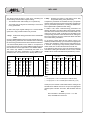
1
MPL 4083
PROCESSOR
High-Tech Made in Switzerland
COMMUNICATION SBC WITH 68360
The MPL4083 is a highly integrated all-CMOS single board computer with 3U form factor. Built around the MC68360 (QUICC)
32-bit controller, the MPL4083 is well suited for applications requiring high performance communication and data management
capability with great flexibility.
Implemented on board the MPL4083 are all major components used to build a complete and sophisticated host system. It
features an SCSI-2 interface for mass storage devices, two types of Ethernet interfaces, an opto isolated CAN interface, various
serial interfaces and several types of memory. The MPL4083 can be further customized with the use of M-Modules. The board
also supports a full 16-bit G-96 bus interface for I/O and memory extension.
The fully CMOS architecture draws a mere 500mA on 5V. This makes the MPL4083 the ideal choice for any low-cost
embedded-control applications, ranging from control, communication, data acquisition and management activities to portable
microcomputer applications.
TECHNICAL FEATURES
•
•
•
•
•
•
•
•
•
•
•
•
Powerful 32-bit 68EN360
Processor speeds 25 MHz or 33 MHz
Two DIL sockets for up to 2 Mbyte Boot ROM
72-pin SIMM for up to 128 Mbyte DRAM
Up to 2 Mbyte SRAM, permanently soldered
Up to 2 Mbyte Flash ROM, permanently soldered (optional)
Two 4 kbit serial EEPROMs
SCSI-2 interface with active termination
Ethernet interfaces 10BaseT and AUI
Isolated CAN bus interface (optional)
Five RS-232 serial ports
Up to 27 TTL Level I/Os
•
•
•
•
•
•
•
•
•
•
•
•
•
Four 16-bit timers
Real Time Clock with calendar
SRAM and RTC are battery protected
Background Debugger Interface
M-Module socket
Full G-96 interface
Compact single height Eurocard design (100 x 160mm)
8-level multilayer design
OS-9 support for all on board functions
Power management features
EMI/RFI protection and filtering of I/O and power lines
Low power CMOS, 500mA typ. @ 5V
Available in extended temperature range
References:
MPL4083-1:
MPL4083-2:
© 1996 by MPL AG
68360 SBC, 25 MHz, 0°C +70°C, 256 kByte SRAM, no Flash ROM, no CAN
68360 SBC, 25 MHz, 0°C +70°C, 512 kByte SRAM, 1 Mbyte Flash ROM, with CAN
1
MEH-10054-001 Rev. C
MPL 4083
High-Tech Made in Switzerland
TABLE OF CONTENTS
INTRODUCTION .............................................................................................................................................................................................. 5
I. ABOUT THIS MANUAL .................................................................................................................................................................... 5
II. SAFETY PRECAUTIONS AND HANDLING ................................................................................................................................... 5
III. ELECTROSTATIC DISCHARGE (ESD) PROTECTION ............................................................................................................... 5
IV. EQUIPMENT SAFETY ................................................................................................................................................................... 5
1. GENERAL INFORMATION AND SPECIFICATIONS .................................................................................................................................. 6
1.1 PRODUCT DESCRIPTION ........................................................................................................................................................... 6
1.2 SPECIFICATIONS ......................................................................................................................................................................... 7
1.3 POWER DISSIPATION MEASUREMENT .................................................................................................................................... 8
1.4 RELATED DOCUMENTATION ..................................................................................................................................................... 9
1.5 DEFINITION OF TERMS .............................................................................................................................................................. 9
2. HARDWARE PREPARATION AND INSTALLATION ................................................................................................................................ 10
2.1 PARTS LOCATION ..................................................................................................................................................................... 10
2.1.1 SWITCH, JUMPER AND CONNECTOR OVERVIEW ................................................................................................ 11
2.2 MEMORY INSTALLATION .......................................................................................................................................................... 11
2.2.1 BOOT ROM INSTALLATION ...................................................................................................................................... 11
2.2.1.1 BOOT ROM TYPE AND SIZE ..................................................................................................................... 11
2.2.1.2 BOOT ROM CONFIGURATION SWITCH (SW2) ....................................................................................... 12
2.2.1.3 BOOT ROM SOCKETS ............................................................................................................................... 12
2.2.2 DRAM INSTALLATION ............................................................................................................................................... 12
2.3 SWITCHES .................................................................................................................................................................................. 12
2.3.1 CONFIGURATION SWITCH (SW1) ............................................................................................................................ 12
2.3.2 BATTERY BACKUP/SCSI TERMINATION SWITCH (SW3) ...................................................................................... 12
2.4 CONNECTORS ........................................................................................................................................................................... 13
2.4.1 G-96 CONNECTOR (J1) ............................................................................................................................................. 13
2.4.2 M-MODULE CONNECTOR (J2) .................................................................................................................................. 14
2.4.3 SIMM CONNECTOR (J3) ............................................................................................................................................ 14
2.4.4 TWISTED PAIR CONNECTOR (J4) ........................................................................................................................... 15
2.4.5 CAN/AUI CONNECTOR (J5) ....................................................................................................................................... 16
2.4.6 I/O CONNECTOR (J6) ................................................................................................................................................ 17
2.4.7 SCSI CONNECTOR (J7) ............................................................................................................................................. 18
2.4.8 BACKGROUND DEBUG CONNECTOR (J8) ............................................................................................................. 18
2.4.9 RESET AND ABORT JUMPERFIELD (J11) ............................................................................................................... 19
2.4.10 APPLYING POWER IN SINGLE BOARD APPLICATIONS ...................................................................................... 19
3. OPERATING INSTRUCTIONS .................................................................................................................................................................. 19
3.1 STATUS INDICATORS ............................................................................................................................................................... 19
3.2 MAIN MEMORY MAP .................................................................................................................................................................. 20
3.3 DETAILED REGISTER MAP ....................................................................................................................................................... 21
3.3.1 EPLD & BOARD REGISTERS OVERVIEW ................................................................................................................ 21
3.4 BOARD INFORMATION REGISTERS ........................................................................................................................................ 22
3.4.1 CONFIGURATION REGISTER (CFG) ........................................................................................................................ 22
3.4.2 HARDWARE INFO REGISTER 1 (HWIR1) ................................................................................................................ 22
3.4.3 HARDWARE INFO REGISTER 2 (HWIR2) ................................................................................................................ 22
3.4.4 EPLD VERSION REGISTER (EVER) ......................................................................................................................... 23
3.5 MC68EN360 ................................................................................................................................................................................ 23
3.5.1 PROGRAMMING THE MC68EN360 ........................................................................................................................... 23
3.5.1.1 MODULE BASE ADDRESS REGISTER (MBAR) ....................................................................................... 23
3.5.1.2 AUTO VECTOR REGISTER (AVR) ............................................................................................................ 23
3.5.1.3 RESET STATUS REGISTER (RSR) ........................................................................................................... 24
3.5.1.4 CLKO CONTROL REGISTER (CLKOCR) .................................................................................................. 24
3.5.1.5 PLL CONTROL REGISTER (PLLCR) ......................................................................................................... 24
3.5.1.6 SYSTEM PROTECTION CONTROL REGISTER (SYPCR) ....................................................................... 24
3.5.1.7 PORT E PIN ASSIGNMENT REGISTER (PEPAR) .................................................................................... 24
3.5.1.8 MODULE CONFIGURATION REGISTER (MCR) ....................................................................................... 24
3.5.1.9 GLOBAL MEMORY REGISTER (GMR) ...................................................................................................... 24
3.5.1.10 BASE & OPTION REGISTER 0 (BR0, OR0) ............................................................................................ 24
3.5.1.11 BASE & OPTION REGISTER 1/2 (BR1/2, OR1/2) ................................................................................... 25
3.5.1.12 BASE & OPTION REGISTER 3 (BR3, OR3) ............................................................................................ 25
3.5.1.13 BASE & OPTION REGISTER 4 (BR4, OR4) ............................................................................................ 25
3.5.1.14 BASE & OPTION REGISTER 5 (BR5, OR5) ............................................................................................ 25
3.5.1.15 BASE & OPTION REGISTER 6 (BR6, OR6) ............................................................................................ 25
3.5.1.16 BASE & OPTION REGISTER 7 (BR7, OR7) ............................................................................................ 25
3.5.1.17 PORT A REGISTERS ................................................................................................................................ 26
3.5.1.18 PORT B REGISTERS ................................................................................................................................ 26
3.5.1.19 PORT C REGISTERS ............................................................................................................................... 26
2
MPL 4083
High-Tech Made in Switzerland
4. FUNCTIONAL AND OPERATIONAL DESCRIPTION ............................................................................................................................... 27
4.1 RESET OPERATION ................................................................................................................................................................... 27
4.2 INTERRUPT STRUCTURE ......................................................................................................................................................... 27
4.2.1 LEVEL 7 INTERRUPT PRINCIPLES .......................................................................................................................... 28
4.2.2 IRQ7-SOURCE REGISTER (ISSR) ............................................................................................................................ 28
4.2.3 PERIPHERAL VECTOR REGISTER (PVTR) ............................................................................................................. 29
4.2.4 PERIPHERAL IRQ-MODE REGISTER (PIMR) .......................................................................................................... 29
4.2.5 PERIPHERAL IRQ-LEVEL REGISTER (PILR) ........................................................................................................... 30
4.3 BOOT ROM ................................................................................................................................................................................. 30
4.3.1 BOOT ROM ACCESS TIME ........................................................................................................................................ 30
4.4 DRAM INTERFACE ..................................................................................................................................................................... 31
4.4.1 DRAM ACCESS TIME ................................................................................................................................................. 31
4.4.2 DRAM PARAMETERS REGISTER (DPAR) ............................................................................................................... 33
4.5 SRAM INTERFACE ..................................................................................................................................................................... 34
4.6 FLASH ROM INTERFACE (OPTION) ......................................................................................................................................... 34
4.7 EEPROM INTERFACE ................................................................................................................................................................ 34
4.7.1 PROGRAMMING NOTE .............................................................................................................................................. 35
4.8 I/O INTERFACE .......................................................................................................................................................................... 36
4.8.1 RS-232 INTERFACE ................................................................................................................................................... 36
4.8.2 TTL INTERFACE ......................................................................................................................................................... 36
4.8.3 SHARED I/O SIGNALS ............................................................................................................................................... 36
4.8.4 I/O CONFIGURATION REGISTER 1 (ICR1) .............................................................................................................. 38
4.8.5 I/O CONFIGURATION REGISTER 2 (ICR2) .............................................................................................................. 39
4.9 ETHERNET INTERFACE ............................................................................................................................................................ 40
4.9.1 TWISTED-PAIR INTERFACE ..................................................................................................................................... 40
4.9.2 AUI INTERFACE ......................................................................................................................................................... 40
4.9.3 ETHERNET CONFIGURATION REGISTER (ETCR) ................................................................................................. 41
4.9.4 ETHERNET STATUS REGISTER (ETSR) ................................................................................................................. 42
4.10 SCSI INTERFACE ..................................................................................................................................................................... 43
4.10.1 SCSI BUS TERMINATION ........................................................................................................................................ 43
4.10.2 TERMINATOR POWER (TERMPWR) ...................................................................................................................... 43
4.11 CAN INTERFACE (OPTION) .................................................................................................................................................... 44
4.11.1 IMPLEMENTATION ESSENTIALS ........................................................................................................................... 44
4.12 M-MODULE INTERFACE .......................................................................................................................................................... 45
4.13 G-96 INTERFACE ..................................................................................................................................................................... 45
4.13.1 SYNCHRONOUS G-96 ACCESSES ......................................................................................................................... 45
4.13.2 ASYNCHRONOUS G-96 ACCESSES ...................................................................................................................... 45
4.13.3 G-96 SIGNAL CONTROL REGISTER (GSCR) ........................................................................................................ 46
4.13.4 G-96 IRQ MODE REGISTER (GIMR) ....................................................................................................................... 46
4.14 REAL TIME CLOCK .................................................................................................................................................................. 47
4.15 BATTERY CIRCUIT .................................................................................................................................................................. 47
5. SUPPLEMENTARY INFORMATION ......................................................................................................................................................... 48
5.1 EMC FEATURES ......................................................................................................................................................................... 48
5.2 POWER SAVING OPTIONS ....................................................................................................................................................... 49
APPENDIX A - INIT CODE EXAMPLE .......................................................................................................................................................... 50
A.1 INTRODUCTORY INFORMATION ............................................................................................................................................. 50
A.2 EXAMPLE CODE LISTING ........................................................................................................................................................ 51
APPENDIX B - SUPPORT INFORMATION ................................................................................................................................................... 56
B.1 CONNECTOR ASSEMBLY KIT .................................................................................................................................................. 56
B.1.1 DISTRIBUTOR ADDRESSES ..................................................................................................................................... 56
B.2 M-MODULE MOUNTING KIT ..................................................................................................................................................... 56
3
High-Tech Made in Switzerland
4
MUX
MUX
RS232 Driver
(ESD protected)
5
SCC4
RS232 Driver
(ESD protected)
6
MUX
RS232 Driver
(ESD protected)
6
MUX
Address
SCC3
4
Flash ROM
max. 2MByte
32-bit wide
Data
Background
Debug
Interface
BDI
Crystal
32.768 kHz
21
Free
Ports
EMI / RFI
Filtering/Protect
SCC1
Ethernet Contr.
LXT901
SPI
Vcc
CPU
68EN360
Twisted pair
Interface
Option
CAN Controller
82C200
Buffers
Buffers
SCSI Controller
53C96
Active termination
G64/96 Interface
(96-pin connector)
M-Modul Interface
(40-pin, A08/D16/INTC)
SCSI Bus Interface
(50-pin connector)
Opto coupl.
& Driver
AUI Interface
RTC 72423
time and
calendar
Battery
160 mAh
6
MPL 4083
Serial
EEPROMs
2 x 4 kbit
SCC2
CAN/AUI Interface
(26-pin conn. / HD)
CAN Interface
Fig. 1.1 Block Diagram MPL4083
DRAM SIMM
max. 128MByte
32-bit wide
Option
4
TTL I/O Interface
SRAM
max. 2MByte
16/32-bit wide
Control SMC1/2
RS232 Driver
(ESD protected)
I/O Interface
(60-pin connector, high density)
RS232 Interface
BootROM
max. 2MByte
16-bit wide
MPL 4083
High-Tech Made in Switzerland
III. ELECTROSTATIC DISCHARGE (ESD) PROTECTION
INTRODUCTION
I. ABOUT THIS MANUAL
Various electrical components within the product are
sensitive to static and electrostatic discharge (ESD). Even a
non-sensible static discharge can be sufficient to destroy or
degrade a component's operation!
This manual assists the installation and initialization procedure by providing all the information necessary to handle and
configure the MPL4083. The manual is partitioned in five
chapters where instructions for hardware installation and
configuration (chapter 2), software initialization (chapter 3)
and functional principles (chapter 4) are given. Product specification and related documentation (chapter 1) as well as
supplementary hardware and programming information
(chapter 5 and Appendix A / B) complete the product description.
Following the precautions listed below will avoid ESD-related
problems:
•
Use a properly installed anti static pad on your work
surface.
•
Wear wrist straps and observe proper ESD grounding
techniques.
•
Leave the unit in its anti static cover until you are prepared
to install it in the desired environment. When it is out of its
protective cover, place the unit on the properly grounded
anti static work surface pad.
For personal safety and safe operation of the MPL4083,
follow all safety procedures described here and in other
sections of the manual.
•
Do not touch any components on the product. Handle the
product by its card edges.
•
IV. EQUIPMENT SAFETY
The manual is written for technical personnel responsible for
integrating the MPL4083 into their system.
II. SAFETY PRECAUTIONS AND HANDLING
Power must be removed from the system before installing
(or removing) the MPL4083 to prevent the possibility of
personal injury (electrical shock) and/or damage to the
product.
•
Handle the product carefully, i.e. dropping or mishandling
the MPL4083 can cause damage to assemblies and
components.
•
Do not expose the equipment to moisture
Great care is taken by MPL that all it's products are thoroughly
and rigorously tested before leaving the factory to ensure that
they are fully operational and conform to specification. However, no matter how reliable a product, there is always the
remote possibility that a defect may occur. The occurrence of
a defect on this device may, under certain conditions, cause
a defect to occur in adjoining and/or connected equipment. It
is the users responsibility to ensure that adequate protection
for such equipment is incorporated when installing this
device. MPL accepts no responsibility whatsoever for such
kind of defects, however caused.
WARNING
There are no user-serviceable components on the
MPL4083!
5
MPL 4083
High-Tech Made in Switzerland
The remaining five serial channels of the QUICC are implemented as RS-232 interfaces. They are partly user
configurable which means that all lines not used for the RS232 interface (except RxD / TxD of SMC1 and 2) can be
defined to function as TTL Level I/Os for free use in the
system. In total, up to 27 lines may be dedicated to that
purpose.
1. GENERAL INFORMATION AND SPECIFICATIONS
This chapter provides a general overview over the MPL4083
and its features. It outlines the electrical and physical specifications of the product, its power requirements and a list of
related publications.
A field bus connection can be implemented via an optional
CAN bus interface (ISO/DIS 11898). The interface is opto
isolated and allows for data rates up to 1 Mbit/sec.
1.1 PRODUCT DESCRIPTION
The MC68360 (QUICC) from Motorola is a versatile one-chip
integrated microprocessor and peripheral combination that
can be used in a variety of controller applications. It particularly excels in communication activities.
The MPL4083 offers a full implementation of the G-96 interface. This opens access to numerous G-96 compatible products and therefore allows for a flexible I/O and memory
extension. Internal logic provides control over some features
of the G-96 interface.
The processor core is the 32-bit version of the CPU32 and is
based on the 68020. Calculating power is about 4.5 MIPS at
25 MHz. An integrated PLL circuit allows to select almost any
frequency up to 25 MHz (33 MHz optional). Additional power
saving options give full flexibility in power critical designs.
Four 16-bit timers, two DMA channels and integrated
modules like bus monitor, watchdog and periodic interrupt
timer are also part of the integration.
One standard mezzanine M-Module slot permits local extension with graphics, process I/O, motion control, interfaces,
analog circuits etc. More than one hundred modules with all
kind of functions are available. The M-Module is mounted to
the CPU board by using bolts. A mounted M-Module uses a
second slot in a rack system.
The base of the communication module is a RISC controller.
It independently supports the six serial channels with different
protocols as there are: Ethernet, HDLC/SDLC, UART,
BISYNC, V.14, X.21, Profibus and more. The autonomous
serial DMA allows for high speed connections to these serial
ports. As an extra, unused port lines can be used as general
purpose I/Os.
All on board/external interrupt sources (G-96, SCSI, M-Module, CAN and RTC) are programmable to be vectored or autovectored. The level of the on board interrupt sources can be
changed by software.
The MPL4083 provides all aspects of quality demanded of an
industrial computer system. Development according to EMC
requirements support the user in achieving the CE conformity
on the system level. This covers features like power saving
options, on board protection/filter devices on power and I/O
lines as well as a carefully designed layout.
The Background Debug Interface is available via a 10-pin
connector (Motorola pin-out).
The MPL4083 comes with two 32-pin JEDEC sockets for up
to 2 Mbytes of Boot ROM (16-bit wide) which allows to install
any type of real-time operating system and/or application.
Battery protected SRAM of up to 2 Mbytes is soldered directly
to the board. 128 Mbytes of DRAM can be installed on the 32bit wide 72-pin SIMM-socket. This is enough even for the most
complex real time application. As an option, up to 2 Mbytes of
32-bit wide Flash ROM may be used to store application
specific code. On-board programming is supported to simplify
installation and updates of the user code.
Software development on the MPL4083 is simplified by the
availability of the OS-9 V3.0 real-time, multitasking operating
system. The integration includes drivers for each on board
function.
External mass storage devices such as hard disk and floppy
disk can be connected to the SCSI-2 interface. The interface
is terminated with an active termination and uses a standard
50-pin header. The SCSI-2 channel is supported by DMA and
allows for data transfers up to 5 Mbytes/sec.
The Ethernet interface allows for two types of LAN connections which, however, cannot be used in parallel. A Twisted
Pair connection (10BaseT) can directly be established via an
on board RJ-45 connector. The Cheapernet implementation
(10Base2) is prepared via an AUI compatible cable connection and requires additionally an external Cheapernet transceiver. The MPL4083 is shipped pre-configured with the
Ethernet address (in a serial EEPROM). The Ethernet interface is supported by local DMA and reaches a data transfer
rate of 10 Mbits/sec.
6
MPL 4083
High-Tech Made in Switzerland
1.2 SPECIFICATIONS
ELECTRICAL
Processor:
32-bit CPU MC68EN360
• 25 MHz, 4.5 MIPS
• 33 MHz optional
• Programmable frequency (32.768kHz crystal)
• Four 16-bit timers
• BD-Interface available
• several monitors and modules
SCSI Interface:
Uses SCSI Controller 53C96
• SCSI-2 compatible
• 8-bit single ended
• active termination, switchable
• LED shows termination status
• on board 50-pin standard header
• 5 Mbytes data transfer (DMA)
Boot ROM:
Two 32-pin JEDEC DIL-sockets
• up to 2 Mbytes
• EPROM, EEPROM or Flash ROM
• 16-bit data bus
Ethernet Interface:
LEDs for RxD and TxD. Two types of interfaces
Twisted Pair:
• 10BaseT standard
• on board isolating transformer
• on board RJ-45 connector, shielded
• UTP or STP connections possible
• all lines are ESD protected
Cheapernet:
• 10Base2 (also -5) with external transceiver
• on board isolating transformer
• all lines are ESD protected
• available at 26-pin connector
• allows 1:1 flat cable wiring to DB-15 (AUI interface)
SRAM:
Up to four TSOP devices, permanently soldered
• up to 2 Mbytes
• battery protected
• 16/32-bit data bus (depends on SRAM size)
• max. 1 wait state
DRAM:
Uses 72-pin JEDEC SIMM modules
• all sizes up to 128 Mbytes
• two banks supported
• 32-bit data bus
• 4-bit parity possible
• page mode operation supported
CAN bus interface (option):
Uses the CAN Controller 82C200
• basic CAN
• opto isolated
• external supply 9V ... 28Vdc, 100mA max.
• power input reverse polarity protected
• ISO/DIS 11898, high speed (1 Mbit/sec)
• input + output delay 270ns max.
• all lines are ESD protected
• available at 26-pin connector
• allows 1:1 flat cable wiring to DB-9 (CiA DS102-1)
Flash ROM (option):
5V programming, two TSOP devices (x16), permanently
soldered
• up to 2 Mbytes
• on board programmable
• 32-bit data bus
• max. 1 wait state
Serial interfaces:
All serial lines are ESD protected
2 SMC ports (SMC1 and 2)
• UART protocol
• 2 x RS-232
• TxD, RxD, RTS, CTS, GND
• available at 60-pin connector
• pinout compatible to MPL4080 / 4082 / 4215
1 SCC port (SCC4)
• UART protocol
• 1 x RS-232
• TxD, RxD, RTS, CTS, DCD, GND
• available at 60-pin connector
2 SCC ports (SCC3 and 2)
• UART protocol
• 2 x RS-232
• TxD, RxD, RTS, CTS, DTR, DCD, GND
• ready for modem
• available at 60-pin connector
Serial EEPROMs:
Two devices, permanently soldered
• 4 kbit, x16 organisation
• connected to SPI of 68360
• pre-configured with ethernet address
Real Time Clock:
• battery protected
• 4-bit parallel interface
• time and calendar
• interrupt may be used
7
MPL 4083
High-Tech Made in Switzerland
TTL I/Os:
Partly shared/muxed with serial ports
• up to 27 TTL I/Os
• Port A2 - A7 (shared/muxed with serial ports)
• Port A10 - A15 (unused I/Os)
• Port C2 - C3 / B13 - B17 (shared with serial ports)
• Port C0 - C1 / C6 - C11 (muxed with serial ports)
• all lines are EMI/ESD protected
• available at 60-pin connector
ENVIRONMENT
Temperature range:
• 0° to +70°C (+32° to +158°F)
• -25° to +85°C (-13° to +185°F) on request
Relative humidity:
• 10% ... 90% non-condensing
1.3 POWER DISSIPATION MEASUREMENT
The power dissipation of the MPL4083 has been determined
under the following conditions: Supply of 5.0 volts, temperature of 25°C, frequency of 25.0 MHz, two 1 Mbit EPROMs, 4
Mbyte DRAM, special test software running under OS-9,
serial communication on one channel , no connection to the
interfaces SCSI (termination is enable), Ethernet (controller is
shut down), CAN, G-96, M-Module, TTL I/Os and BDM.
M-Module interface:
One M-Module slot
• A08 / D16 / INTA / INTC
• requires an additional G-96 slot
• Mounting kit available
G-96 interface:
Full G-96 support
• 32 Mbytes VMA space
• Separate 1 kWord spaces for VPA synch./asynch.
The measurement results show, that the power dissipation is
almost independent of the product version (MPL4083-1 or -2).
The variation of the current consumption over the
temperature range -25°C to +85°C stays in a close band of
approx. +/- 30mA.
Miscellaneous:
• Battery with capacity of 160mAh
• LEDs for Power, and HALT/RESET
• RESET and ABORT jumperfield
• IRQ levels are programmable
• IRQ level 7 source detection
• User definable 8-bit configuration switch
• Size detect for DRAM,SRAM and Flash ROM
• Selectable G-96 clocking strategy
• RS-232 drivers can be shut down
• EMI/RFI protection/filtering of I/O and power lines
The typical values given in the Table below are design helps
only. In the "idle" state the system does not process any tasks.
It is put to sleep and awakened every ten milliseconds by a
time slice generator. In the "running" state the system processes special tasks which take up 100% processing time.
The values for 33.34 MHz are not yet defined. It should be kept
in mind that the MPL4083 will dissipate much more power
when integrated in a system where all interfaces are connected!
PHYSICAL/POWER
Frequency
Idle
Running
Form factor:
• 3U, 100mm x 160mm (single eurocard)
• 1 slot without, 2 slots with M-Module
25.0 MHz
33.34 MHz
380mA
t.b.d.
470mA
t.b.d.
Height:
• Top layer:
Bottom layer:
Table 1.4 Power Dissipation MPL4083
15mm max.
3mm max.
Power dissipation can further be reduced by using the power
management features offered by the QUICC and the
MPL4083 on board components. For example, a shut down of
the RS-232 drivers saves up to 45mA. Disabling the SCSI
active termination saves approx. 20mA. On the other hand,
enabling the Ethernet Controller (LXT901) adds approx.
45mA.
Weight:
• 165 gr. typical
Input Power Range:
All lines are protected by ESD devices
• +5V:
4.80VDC - 5.25VDC
• +12V:
+12.0VDC +/- 10%
• -12V:
-12.0VDC +/- 10%
Power consumption:
• +5V:
typ. 500mA @ 25 MHz
• +12V:
required for AUI and M-Module
• -12V:
required for M-Module
8
MPL 4083
High-Tech Made in Switzerland
1.4 RELATED DOCUMENTATION
The following publications are applicable to the major on
board components and interfaces and may provide additional
helpful information:
The high integration level of the QUICC offers a lot more
features than could possibly be described within the scope of
this manual. A set of two data books gives detailed information
about the QUICC and its modules. Supplied by Motorola,
these books are:
•
On board components:
• Flash ROM 29x00 data sheet (Fujitsu or AMD)
• Ethernet Controller LXT901 data sheet (Level One)
• SCSI Controller 53C96 data sheet (NCR/Symbios Logic
or AMD)
• Real Time Clock RTC72423 data sheet (Seiko)
• CAN Controller PCA82C200 data sheet (Philips)
• Serial EEPROM 93C66 data sheet (several manufacturers)
MC68360 (QUICC) User's Manual Rev 1.
This manual describes the capabilities, operation and
functions of the QUICC, including the electrical characteristics and timing information. This manual is available at
Motorola's web site in Acrobat Reader format (.pdf, split in
three parts). The web address is listed below.
•
Interfaces:
• "Ethernet" Standard (ISO / IEC 8802-3 : 1993 or
ANSI / IEEE 802.3, 1993 Edition).
This standard includes specifications for 10Base5
(Ethernet), 10Base2 (Cheapernet) and 10BaseT (Twisted
Pair).
• SCSI-2 Standard (ANSI X3.131-199x)
• CAN Specification (Robert Bosch 199x)
• G-64/96 Specification Rev. 3 (Gespac, Switzerland)
• M-Module Specification Rev. 2.2 (MUMM, Germany)
CPU32(+) Reference Manual.
The reference manual describes the capabilities, operation and programming of the CPU32(+) instruction
processing module which is the core processor of most
M68300 family members.
Detailed information can be found on Motorola's web site. As
of the writing of this manual, following links may be used:
•
http://www.mot.com
1.5 DEFINITION OF TERMS
This is the Mototrola home page.
•
Memory addresses used throughout this manual relate to the
memory maps given in this manual. Signal and register
names and their corresponding abbreviations relate to the
denotation used in the respective device data sheets and
user's manuals.
http://www.mot-sps.com/sps/General/chips-nav.html
Is the entry point to comprehensive information regarding
Motorola Semiconducdors including
- Manuals
- Erratas
- Examples
- Frequently Asked Questions (FAQ)
9
MPL 4083
High-Tech Made in Switzerland
2. HARDWARE PREPARATION AND INSTALLATION
This chapter provides hardware preparation and installation instructions for the MPL4083. It describes the setting of the on
board memory and the corresponding switches, and supplies information about interfaces, connectors and jumpers.
2.1 PARTS LOCATION
The diagram of Fig. 2.1 identifies the position of all components, jumpers, switches, LEDs, connectors and sockets on the
MPL4083 top and bottom layer.
2
60 30
29
J7
1
U50
U15
C84
U55
U18
RN3
50
2
49
1
U13
J8
10
2
9
1
10
J9
SW1
RN4
BootROM Future
type & size use
9
J10
U4
M-Module
connector
U25
X2
J6
J11
4 3
1 2
SW3
U10
I/O interface
connector
U27
U5
U41
U54
U26
32 2
31 1
U42
U53
J1
U8
X3
+
J5
U9
R146
OC2
U44
T2
2
U39
U32
RN7
U40
U33
U21
U3
U38
J4
8
U23
RN5
U17
U20
J3
1
TR1
7
U2
+
1
1
TR2
14
Boot ROM
sockets
39 40
U22
TS9
2
71
72
DRAM SIMM
connector
C64
+
+
TS7
C44
TS1
U19
U37
C32
T6
U12
U11
Fig. 2.1 Parts Location
10
T3
U16
C46
C31
U47
U48
U30
U28
+
C52
T4
U49
C77
U31
+
U58
U29
+ C36
U52
+
U57
RN1
+
U51
RN6
U36
+ C34
U56
F1
U60
D3
U59
RN2
U14
+
+ C89
U43
+ C35
T5
+ C16
U61
TS4
Power OK
(green)
TS2
U46
T1
+
+ C118
D18
LED1 LED3
Halt/Reset
(red)
LED2
Ethernet
TxD (green)
TS3
U35
TS10
LED5 LED4
Ethernet
RxD (green)
C12
+ C68
+ C71
U34
TS8
SCSI
Termination
(green)
G-96
connector
U1
X1
U45
SW2
U7
OC1
26 13
25 12
Twisted-pair
connector
U24
U6
CAN/AUI interface
connector
Abort &
Reset
J2
59
Background 8-Bit
Battery & MPL use
debug conn. configuration SCSI Term. only
BT1
SCSI
connector
MPL 4083
High-Tech Made in Switzerland
2.1.1 SWITCH, JUMPER AND CONNECTOR OVERVIEW
The following Table gives an overview of the switches, jumpers, connectors and sockets that may need to be configured.
Name
Function
SW1
SW2
SW3
U24
U25
J1
J2
J3
J4
J5
J6
J7
J8
J9
J10
J11
Configuration switch (8-bit)
Boot ROM configuration switch
Battery backup/SCSI Termination switch
Boot ROM socket (even byte)
Boot ROM socket (odd byte)
G-96 connector
M-Module connector
SIMM connector
Twisted Pair connector
CAN/AUI connector
I/O connector
SCSI connector
Background Debug connector
For MPL use only. Do not connect!
For future use. Do not connect!
Reset and Abort jumperfield
2.2.1.1 BOOT ROM TYPE AND SIZE
The following Table details the type and size of memory
devices that may be used. The data width of the devices must
be x8. The size may range from 256 kBit up to 8 Mbit, whereat
any binary interstep is possible.
Table 2.1.1 Switch, Jumper and Connector Overview
Type
Sizes
EPROM (1)
256 k - 8 Mbit 28-pin or 32-pin DIL packages may be used.
EEPROM (2)
512 k - 4 Mbit 32-pin DIL packages only
must be used. On board
programming is possible
(read/write). The devices
may be hardware write
protected (read only).
Flash ROM (2)
(5V)
256 k - 4 Mbit 32-pin DIL packages only
must be used. On board
programming is possible
(read/write). The devices
may be hardware write
protected (read only).
Flash ROM
(12V)
256 k - 4 Mbit 32-pin DIL packages only
must be used. On board
programming is NOT
possible (no 12V support). The devices are
read only.
2.2 MEMORY INSTALLATION
Four major memory blocks are located on the MPL4083: Boot
ROM, DRAM, SRAM, Flash ROM and EEPROM.
SRAM, Flash ROM and EEPROM are soldered directly to the
board and need not to be configured. The size of SRAM and
Flash ROM can be determined by reading the Hardware Info
Register 1 (HWIR1), see 3.4.2. The configuration of the Boot
ROM and DRAM is described in the following paragraphs.
Comment
Table 2.2.1.1 Boot ROM Type and Size
Notes:
(1)
If you use 1 Mbit EPROMs be sure to use JEDEC types. There are
EPROMs available with a MaskROM compatible pin out which is
not compatible to the JEDEC pin out (examples of these incompatible Mask ROM versions are NEC27C1000, TC571001,
Am27C100). These types are not supported.
(2)
If EEPROM and 5V-Flash ROM are to be programmed on board,
they have to support the Alternative Timing method. This means
that write operations are CE controlled, rather than WE controlled.
Most manufacturers now support this feature.
2.2.1 BOOT ROM INSTALLATION
The following paragraphs provide the information necessary
to install the Boot ROM.
11
MPL 4083
High-Tech Made in Switzerland
2.2.1.2 BOOT ROM CONFIGURATION SWITCH
(SW2)
2.2.2 DRAM INSTALLATION
Switch SW2 defines the various configurations of the Boot
ROM. All combinations not shown are invalid and may lead to
erratic behaviour or even damage the board or devices.
The DRAM interface is 32-bit wide and consists of one SIMM
socket (J3). The implementation of the 68360 DRAM controller and the design of the MPL4083 support types and features
of DRAM SIMMs as follows:
EPROM:
•
•
256k
1
2
3
4
5
6
7
8
ON
512k/1M
1
2
3
4
5
6
7
8
ON
2M
1
2
3
4
5
6
7
8
4M
ON
1
2
3
4
5
6
7
8
ON
Flash ROM (5V):
All devices (256k-4Mbit)
EEPROM:
All devices (512k-4MBit)
1
2
3
4
5
6
7
8
8M
1
2
3
4
5
6
7
8
ON
•
•
•
•
•
Standard 72 pin SIMMs.
SIMMs with or without parity (data organization x36 or
x32). Byte-level parity is supported.
Single or double sided SIMMs.
Two banks on one SIMM. (CS1/RAS1 = bank0, CS2/
RAS2 = bank1).
Page Mode and Early Write are supported.
All sizes up to 128 Mbytes. Usually, non-quadratic SIMM
sizes consist of two banks (e.g. 8 MB or 32 MB or 128 MB).
Detection of speed and size of SIMM. The value is read at
the DRAM Parameters Register (DPAR), see 4.4.2.
Note
The SIMM socket as well as the module provide
polarization posts which prevents from wrong insertion.
2.3 SWITCHES
ON
Write protected
Read / Write
This paragraph describes the setting of the remaining
switches.
2.3.1 CONFIGURATION SWITCH (SW1)
This 8-bit configuration switch is free for use. Each switch set
to the ON position is read as a zero. The value can be
determined at the Configuration Register (CFG), see 3.4.1.
Flash ROM (12V):
1
2
3
4
5
6
7
8
1
2
3
4
5
6
7
8
ON
4M
1
2
3
4
5
6
7
8
ON
256k/512k
1M/2M
ON
Fig. 2.2.1.2 Boot ROM Configuration
Fig. 2.3.1 Configuration Switch SW1
2.3.2 BATTERY BACKUP/SCSI TERMINATION
SWITCH (SW3)
Battery backup of SRAM and Real Time Clock (RTC) as well
as SCSI termination enable or disable are selected at dipswitch SW3. Each switch set to the ON position enables the
corresponding function.
2.2.1.3 BOOT ROM SOCKETS
1
2
3
4
The Boot ROM must be installed on the 32-pin DIL sockets
U24 and U25. The upper byte (D31-D24) is located at U24, the
lower byte (D23-D16) at U25. The Boot ROM is accessed as
a 16-bit bank and uses the Global CS (CS0) of the QUICC.
Note
Memory chips in 28-pin DIL packages must be
bottom-aligned, i.e. pin 1 of the chip meets pin 3 of
the socket.
ON
No. #1:
No. #2:
No. #3:
No. #4:
Battery backup enable RTC
Battery backup enable SRAM
SCSI Termination enable (manual)
SCSI Termination enable (auto)
Fig. 2.3.2 Battery Backup/SCSI Term. Switch (SW3)
Switch #4 (auto) has priority over switch #3 (manual). If switch
#4 is enable, the SCSI termination is under software control.
For a more detailed description, refer to 4.10.1.
12
MPL 4083
High-Tech Made in Switzerland
2.4 CONNECTORS
The following paragraphs describe the attachment of the several interfaces to the appropriate connectors.
2.4.1 G-96 CONNECTOR (J1)
The G-96 bus interface is available at connector J1. The connector is of type DIN41612, male and with 96 pins.
Table 2.4.1 gives a list of the signals that are used by the MPL4083. G-96 signals not mentioned in the Table below are not
connected on the MPL4083. The column "type" represents the view from the MPL4083.
Signal
Type
Description
Comment
D0 - D15 (1)
A0 - A23
/VPA
/VMA
/DS1, /DS0
R/W
/BR, /BGACK
/BG
/IRQ1 -5, /NMI
/RES (2)
E
SYCLK
/IACK
/BERR
/HALT
/DTACK
/PWF (3)
/Page
CHOUT
VBB (4)
+5V (5)
+/-12V (5)
GND (5)
I/O
Out
Out
Out
Out
Out
In
Out
In
OC Out
Out
Out
Out
In
In
In
In
Out
Passive
In
In
In
In
Data lines
Address lines
Valid peripheral signal
Valid memory address
Data strobes upper/lower
Read/Write signal
Bus request/acknowl.
Bus grant
Interrupt lines
Reset
CPU Enable
System clock
Interrupt acknowledge
Bus error
CPU halts
Data acknowledge
Power fail
Memory expansion
Daisy chain out
Power
System Power Input
System Power Input
System Power Input
Internally connected to D16 - D31
Internally connected to A1 - A24
Valid within 1 kword
Covers full memory range of 32 MB
Valid during VPA and VMA cycles
Selects data direction
Used for bus arbitration
Used for bus arbitration
/IRQ6 does not exist
Connected to RESETS
1/16 or 1/32 of CPU clock
1/1 or 1/2 of CPU clock
Acknowledge for vectored IRQ levels
Wired-and with the on board BERR
All G-96 outputs go high-Z
Terminates asynch. data accesses
Releases a level 7 interrupt
Connected to CPU address line A25
Pulled up to +5V
Ext. battery supplies SRAM/RTC
Power input to the MPL4083
Power input to the MPL4083
Power input to the MPL4083
Table 2.4.1 G-96 Bus Connector
Notes:
(1)
Data on the G-96 bus is inverted.
(2)
RESET is an open collector output but NOT bi-directional.
(3)
In older G-64 bus designs (prior to 1984), pin 29a is a -5V input and has to be open. Since then, pin 29a has changed its function and has
become a Power Fail input which is supported by the MPL4083 (level 7 interrupt).
(4)
The external battery connects directly (via schottky diodes) to the SRAM and RTC and cannot be switched off on board. Refer to 4.15
(5)
These are the power inputs to the MPL4083. No other inputs must be used to power the board. Refer to 2.4.10 for more information
For more detailed signal information refer to the G-64/96 Specifications Manual Rev. 3.
Note
On the rear side of the connector a sticker with the board's Ethernet Address is provided.
13
MPL 4083
High-Tech Made in Switzerland
2.4.2 M-MODULE CONNECTOR (J2)
The M-Module connector is a female two row receptacle with 40 pins.
The M-Modules to be used should be of type A08/D16. The INTC feature is supported by the MPL4083. Other types of MModules may be used, however, their compatibility must be checked first.
Table 2.4.2 gives a brief overview over the M-Module signals as supported by the MPL4083. Signals not mentioned in the Table
below are not connected on the MPL4083. The column "type" represents the view from the M-Module.
Signal
Type
Description
Comment
D0 - D15 (1)
A1 - A7 (1)
/CS
/DS1,/DS0
R/W (1)
/IRQ
/RES
CLK
/IACK
/DTACK
+5V,+/-12V
GND
I/O
In
In
In
In
Out
In
In
In
Out
In
In
Data lines
Address lines
Chip Select
Data strobes upper/lower
Read/Write signal
Interrupt line
Reset
Module clock
Interrupt acknowledge
Data acknowledge
System Power
System GND
Connected to D16 - D31
Connected to A1 - A7
Selects the M-Module
Valid during any access
Selects data direction
Connected to RESETS
16 MHz
Acknowledge for vectored IRQs
Terminates accesses
Table 2.4.2 M-Module Connector
Note:
(1)
These signals are buffered. All other signals are directly connected to the devices on the MPL4083.
For more detailed information about the M-Module interface signals refer to the M-Module Specification from MEN, Germany.
For proper mounting of the M-Module, MPL AG offers a mounting kit. Please refer to Appendix B.2.
2.4.3 SIMM CONNECTOR (J3)
This connector is compatible to the JEDEC standard and accepts any appropriate 72-pin DRAM SIMM. Single and double
sided SIMMs may be used. A SIMM placed to its final position will be in parallel to the board thus reducing the overall height
of the board. This prevents from losing an additional slot in a rack system.
Table 2.4.3 gives a brief overview over the SIMM signals as supported by the MPL4083. Signals not mentioned in the Table
below are not connected on the MPL4083. The column "type" represents the view from the SIMM.
Signal
Type
Description
Comment
D31 - D0
A11 - A0 (1)
DP3-0
CAS3-0
RAS0/2
RAS1/3
WE (1)
PD4-PD1
I/O
In
I/O
In
In
In
In
Out
Data lines
Muxed Address lines
Data Parity lines
Column Strobes
Row Strobes bank0
Row Strobes bank1
Write Enable
Presence Detect
Connected to D31 - D0
Connected to A13 - A2
Connected to PRTY0-3
Byte wise selection
Connected to RAS1 (CS1)
Connected to RAS2 (CS2)
Connected to R/W
Readable at DPAR
Table 2.4.3 DRAM SIMM Connector
Note:
(1)
These signals are buffered. All other signals are directly connected to the devices on the MPL4083.
14
MPL 4083
High-Tech Made in Switzerland
2.4.4 TWISTED PAIR CONNECTOR (J4)
The Twisted Pair (TP or 10BaseT) interface is available at connector J4. The connector is of type RJ-45. The integrated
shielding is connected to system ground, therefore allowing for shielded and unshielded connections. Only four of the eight
pins are used to build the interface. The connection is non-crossed. The column "type" represents the view from the MPL4083.
Pin
Signal
Type
Description
1
2
3
4
5
6
7
8
TPTX+
TPTXTPRX+
N.C.
N.C.
TPRXN.C.
N.C.
Out
Out
In
Transmit Data +
Transmit Data Receive Data +
open
open
Receive Data open
open
In
Table 2.4.4 TP Connector
Note:
The chosen connection type, shielded (STP) or unshielded (UTP), must be reflected in the initialization sequence of the Ethernet controller
LXT901. Refer to 4.9 for more information.
15
MPL 4083
High-Tech Made in Switzerland
2.4.5 CAN/AUI CONNECTOR (J5)
The CAN/AUI connector J5 is a male 26 pin, high density connector. It contains both CAN and AUI interface. Each interface
is available separately on an individual connector row and allows for connection with standard ribbon cables.
The upper row of the connector (pins 1 - 13) contains the opto isolated CAN interface, requiring external supply. If a flat cable
connection is used, then the first nine pins of the CAN interface cable build a one-to-one wiring to a DB-9 connector where pin
9 of the cable meets pin 1 of the DB-9. In this way, the pin out of the DB- 9 connector will conform to the Draft Standard DS1021 as described by CiA (CAN in Automation).
The remaining four lines (pins 10 - 13) may be used to connect two LEDs to the Transmitter and Receiver of the Ethernet
Controller (additional to the on board LEDs). However, no limiting resistor is provided and the maximum sink current of these
active low outputs is 2mA.
The lower row (pins 14 - 26) contains the AUI interface. If standard flat cable is to be used, then a one-to-one wiring to a DB15 connector is possible. In this way, the connection will conform to the AUI interface standard as required by most external
transceivers. Note that pin 1 of the cable must meet pin 1 of the DB-15. Cable pins 14 and 15 are not available which, however,
gives no functional impact to the connection.
Table 2.4.5A and 2.4.5B list the signals used by the MPL4083. The column "type" represents the view from the MPL4083.
Please refer to 4.9.2 and 4.11 for a more detailed description of AUI and CAN interface.
Lower Row (AUI):
Upper Row (CAN):
Pin
Signal
Type
1
2
3
4
5
6
7
8
9
10
11
12
13
N.C.
Vext
N.C.
N.C.
C-GND
CANH
CANL
C-GND
N.C.
GND
LEDT
LEDR
VCC
open
In
open
open
In
I/O
I/O
In
open
Power
Out
Out
Out
Description
Ext. Input 9 - 28 Vdc
Ext. CAN Ground
CAN bus line High
CAN bus line Low
Ext. CAN Ground
System GND
Transmit LED Ethernet
Receive LED Ethernet
System +5Vdc
Table 2.4.5A CAN Interface Connector
Pin
Signal
Type
Description
14
15
16
17
18
19
20
21
22
23
24
25
26
GND
COL COL +
TxD TxD +
GND
GND
RxD RxD +
+12V (1)
GND (2)
GND
N.C.
Power
In
In
Out
Out
Power
Power
In
In
Out
Power
Power
open
System GND
Collision Collision +
Transmit Data Transmit Data +
System GND
System GND
Receive Data Receive Data +
System +12Vdc
System GND
System GND
Table 2.4.5B AUI Interface Connector
Notes:
(1)
The +12Vdc outputs may supply an external AUI transceiver. It is protected against current back flow and overcurrent (diode and electronic
fuse).
(2)
This pin is the power return line of the external transceiver.
Refer to Appendix B.1 for support information on the availability of the mating ribbon cable connector.
16
MPL 4083
High-Tech Made in Switzerland
2.4.6 I/O CONNECTOR (J6)
The I/O connector is a male 60 pin, high density connector. It contains both the RS-232 interface and the TTL interface. Each
interface is available separately at an individual connector row and allows for connection with standard ribbon cables.
The upper row (pins 1 -30) contains the RS-232 lines of serial channels SCC2 - SCC4 and SMC1/2. The serial channels SMC1
and 2 are available at pins 21 - 30. If these ten signals are connected to a 10 pin ribbon cable connector, they will form an
interface which is fully compatible to the serial interfaces of MPL products, as there are MPL4215, MPL4080/B and MPL4082.
The lower row (pins 31 - 60) contains unbuffered TTL level I/O signals originating at the QUICC ports A, B and C.
Most of the signals of the upper and lower row are shared and cannot be used at the same time. They can be combined to four
groups, representing their functional type. Please refer to "4.8 I/O Interface" for a more detailed explanation.
•
•
•
Group A: Available in parallel in both RS-232 and TTL area.
Group B: Available in the TTL area only, if the corresponding RS-232 drivers are shut down
Group C: Available individually in the TTL area, if the corresponding analog multiplexer is switched. All these signals
originate at 68360 port C.
Group D: Dedicated to a single connector pin.
•
The first column in the Table below contains the group indication. The column "type" represents the view from the MPL4083.
Upper Row (RS-232):
Lower Row (TTL I/O):
Grp. Pin Signal
Type
QUICC
Port Pin
QUICC
Module
Grp. Pin Signal
A
B
A
C
Out
In
Out
In
Power
Out
In
Out
In
Out
In
Power
Out
In
Out
In
Out
In
Power
In
Out
In
Out
In
Power
Out
In
Out
In
Power
PA3
PA2
PB13
PC6
System GND
PC2
PC7
PA5
PA4
PB14
PC8
System GND
PC3
PC9
PA7
PA6
PB15
PC10
System GND
PC11
PB6
PB7
PB16
PC0
System GND
PB10
PB11
PB17
PC1
System GND
SCC2
SCC2
SCC2
SCC2
A
B
A
B
A
B
D
D
D
D
D
D
1
2
3
4
5
6
7
8
9
10
11
12
13
14
15
16
17
18
19
20
21
22
23
24
25
26
27
28
29
30
A
C
A
B
A
C
A
C
A
B
A
C
C
D
D
A
C
D
D
A
C
TxD2
RxD2
RTS2
CTS2
GND
DTR2
DCD2
TxD3
RxD3
RTS3
CTS3
GND
DTR3
DCD3
TxD4
RxD4
RTS4
CTS4
GND
DCD4
TxD5
RxD5
RTS5
CTS5
GND
TxD6
RxD6
RTS6
CTS6
GND
GP I/O
SCC2
SCC3
SCC3
SCC3
SCC3
GP I/O
SCC3
SCC4
SCC4
SCC4
SCC4
A
A
A
A
A
C
C
A
A
C
C
C
C
C
C
SCC4
SMC1
SMC1
GP I/O
GP I/O
SMC2
SMC2
GP I/O
GP I/O
PA3 (1)
PA2 (1)
PA5 (1)
PA4 (1)
PA7 (1)
PA6 (1)
PA10
PA11
PA12
PA13
PA14
PA15
GND
PB13
PB14
PB15
PB16
PB17
PC0
PC1
PC2
PC3
PC6
PC7
PC8
PC9
PC10
PC11
GND
VCC
QUICC Pin Function
I/O
I/O
I/O
I/O
I/O
I/O
I/O
I/O
I/O
I/O
I/O
I/O
Power
I/O
I/O
I/O
I/O
I/O
I/O
I/O
I/O
I/O
I/O
I/O
I/O
I/O
I/O
I/O
Power
Power
GP I/O
GP I/O
GP I/O
GP I/O
GP I/O
GP I/O
GP I/O
GP I/O
GP I/O
GP I/O
GP I/O
GP I/O
System GND
GP I/O
GP I/O
GP I/O
GP I/O
GP I/O
GP I/O
GP I/O
GP I/O
GP I/O
GP I/O
GP I/O
GP I/O
GP I/O
GP I/O
GP I/O
System GND
System +5VDC
Table 2.4.6B TTL I/O Connector Area
Table 2.4.6A RS-232 Connector Area
Note:
(1)
31
32
33
34
35
36
37
38
39
40
41
42
43
44
45
46
47
48
49
50
51
52
53
54
55
56
57
58
59
60
Type
Due to an implementation error, these signals are reversed by pairs.
17
MPL 4083
High-Tech Made in Switzerland
Warning
Although the design of the I/O interface allows contention-free connection of all external signals at the same
time, contentions may be induced by an incorrect initialization of the 68360 port pins. Avoid such a situation,
it could damage components on the MPL4083.
Refer to Appendix B.1 for support information on the availability of the mating ribbon cable connector.
2.4.7 SCSI CONNECTOR (J7)
The SCSI connector is a 50-pin pin header. The connector's pin out and its signals are compatible to 8-bit single-ended SCSI
bus implementations. Standard 50 pin flat cable may be used to connect the SCSI devices to the MPL4083.
The MPL4083 supplies the TERMPWR line. A diode prevents current back flow and therefore allows other SCSI units to supply
this line as well. The TERMPWR line is protected against overcurrent by an electronic fuse.
The MPL4083 contains internal components to provide switchable Active Termination on the SCSI bus. The Termination can
be enabled at switch SW3.
For more detailed information about the SCSI interface, please refer to 4.10 and the SCSI-2 Standard.
Warning
There is no connector frame that could prevent from misaligned or mirrored cable insertion. Pay attention on
the orientation and position of pin 1 when connecting the cable. The total SCSI cable length must not exceed
6 meters.
2.4.8 BACKGROUND DEBUG CONNECTOR (J8)
Connector J8 is a 10-pin pin header and offers an interface to interconnect the on-chip 68360 background debug monitor to
external debug hard- and software. The connector pin out is compatible to Motorola's definition.
Pin
Signal
Description
1
2
3
4
DS
BERR
GND
BKPT /
DSCLK
GND
FREEZE
RES
IFETCH /
DSI
VCC
IPIPE0
DSO
Data strobe
Bus error
Ground
Breakpoint to the 68360
Serial clock in Background Debug Mode (BDM)
System GND
CPU acknowledged a breakpoint
Connected to RESETH
Instruction word fetch
Serial input data in BDM
System +5Vdc
Used for the instruction pipeline
Serial output data in BDM
5
6
7
8
9
10
Table 2.4.8 Background Debug Connector
Warning
There is no connector frame that could prevent from misaligned or mirrored cable insertion. Pay attention on
the orientation and position of pin 1 when connecting the cable.
18
MPL 4083
High-Tech Made in Switzerland
2.4.9 RESET AND ABORT JUMPERFIELD (J11)
3. OPERATING INSTRUCTIONS
This 2x2 jumper field has two functions:
This chapter provides the necessary information to use the
MPL4083 in various configurations. This includes memory
map details and software initialization of the board as far as
possible.
A reset switch can be connected between pins 1-4. A closure
on this switch releases a system reset (performs a hard reset
to the QUICC) and resets all MPL4083 devices and interfaces.
An external abort switch can be connected between pin
positions 2-3. A closure on this switch will cause a level 7
interrupt. The interrupt source of a level 7 interrupt can be
determined by reading a specially provided interrupt status
register, see 4.2.2.
1
2
4
3
Reset Switch
Abort Switch
3.1 STATUS INDICATORS
The MPL4083 provides five status indicator LEDs, giving the
user visual response to selected functions. The LEDs are
mounted on the solder side at the upper card front. Please
refer to Figure 2.1 for their exact location.
• POWER Indicator LED1:
Fig. 2.4.9 Abort and Reset Jumperfield
2.4.10 APPLYING POWER IN SINGLE BOARD
APPLICATIONS
In each case, power to the MPL4083 must be applied at G-96
connector J1. All other connectors which do have power pins
as well MUST NOT be used to power the board. The required
supply voltages are +5V, +12V and -12V.
In a single board application where the MPL4083 is not
mounted on a G-96 backplane, the +5 Vdc power supply must
be connected to the following pins of J1:
+5V:
Pins 31A, 31B, 31C
GND: Pins 1A, 1B, 1C, 32A, 32B, 32C and 13C, 19C
To insure solid +5V and GND, it is recommended to connect
as many pins as possible to the power supply.
The power dissipation of the MPL4083 is 500mA @ +5V typ,
without connected interfaces (refer also to 1.4). The maximum
dissipation including all interfaces will be much higher.
+12V are required to supply the ethernet AUI port and the MModule. The +12V may be omitted, if the M-Module and AUI
port are not used or do not need to be supplied by the
MPL4083. -12V are only required to supply the M-Module and
may be omitted, if the M-Module is not used or does not need
to be supplied by the MPL4083.
The green Power LED indicator is lit whenever +5V power is
applied to the board.
• HALT/RESET Indicator LED3:
The red Reset/Halt LED indicator is lit whenever the QUICC
Hard Reset or Halt pin is low (asserted).
• Ethernet TxD Indicator LED5:
The green Ethernet TxD LED indicator blinks whenever the
LXT901 controller is transmitting data through one of the
Ethernet ports TP or AUI. It is lit permanently when the LXT901
is in power down mode.
• Ethernet RxD Indicator LED4:
The green Ethernet RxD LED indicator blinks whenever the
LXT901 controller is receiving data from one of the Ethernet
ports TP or AUI.
• SCSI Termination Indicator LED2:
The green SCSI Termination LED indicator is lit whenever the
Active SCSI Termination is enabled.
If used, the +12Vdc and -12Vdc power inputs must be connected to following pins of J1:
+12V:
Pin 30A
-12V:
Pin 30B
The power dissipation of each power input depends on the
application, however, should be less than 1A.
Warning
It should be kept in mind that the MPL4083 will
dissipate much more power when integrated
in a system where all interfaces are connected!
19
MPL 4083
High-Tech Made in Switzerland
3.2 MAIN MEMORY MAP
The MPL4083 uses devices of different bus sizes. 8-bit wide devices are connected to data lines D31-D24, 16-bit wide devices
to D31-D16 and 32-bit wide devices to D31-D0.
The memory map below is valid if the operating system OS-9 as supplied by MPL AG is running. If the MPL4083 is operated
without operating system, then the memory map has to be understood as a proposal and may be changed since the QUICC
allows for adjustable base addresses for each Chip Select (CS0-7). However, two restrictions must be observed when doing
so:
Chip Select 5 (CS5):
•
•
It MUST start on $2000000 boundaries (Base address = n x $02000000; n= 1,2,3,4,...).
Its size is fixed to 32 MB.
Chip Select 7 (CS7):
•
•
It MUST start on $4000000 boundaries (Base address = n x $04000000; n= 1,2,3,4,...).
Its size is fixed to 64 MB.
The column "CS" in the Table below states to which QUICC Chip Select the memory ranges are connected to. Memory
addresses used throughout this manual relate to the memory map above.
Address
Size
Width
CS
Accessed Device
Comment
00000000
00200000
00201000
02000000
02800000
03000000
03800000
05000000
06000000
07000000
08000000
09000000
09800000
0A000000
10000000
2 MB
4k
4k
8 MB
8 MB
8 MB
8 MB
2k
2 MB
2 MB
16 MB
8 MB
8 MB
32 MB
128 MB
16
32
32
8
8
8
8
16
16/32
32
16
16
16
16
32
CS0
internal
internal
CS5
CS5
CS5
CS5
CS6
CS3
CS4
CS7
CS7
CS7
CS7
CS1/2
Boot ROM
Maximum size 2MB
MC68360 Dual Port RAM
MC68360 Internal Registers
EPLD & Board Registers
Only 16 bytes used
Real Time Clock Registers
Only 16 bytes used
SCSI Controller Registers
Only 16 bytes used
CAN Controller Registers
Only 32 bytes used
SCSI DMA Pseudo Address
Only 1 byte used
SRAM
Maximum size 2 MB
Flash ROM
Maximum size 2 MB
M-Module A08 / D16 / INTC
Only 256 bytes used
G-96 bus: VPA synchronous
Only 1 kword used
G-96 bus: VPA asynchronous Only 1 kword used
G-96 bus: VMA
DRAM (two SIMM banks)
Maximum 64 MB each
Table 3.2 Memory Map
20
MPL 4083
High-Tech Made in Switzerland
3.3 DETAILED REGISTER MAP
The memory map in Table 3.2 describes various devices with extended register maps. Refer to the following items for more
information about these devices and their maps:
Device
Complete Information
Refer also to
EPLD & Board Registers
MC68360
SCSI Controller
CAN Controller
M-Module
G-96
Real Time Clock
In this Manual
User's Manual Rev.1
53C96 data sheet
PCA82C200 data sheet
Data sheet of module used.
Data sheet(s) of appropriate bus board(s) used
RTC72423 data sheet
3.3.1
3.5
4.10
4.11
4.12
4.13
4.14
Table 3.3 Device Index
3.3.1 EPLD & BOARD REGISTERS OVERVIEW
These registers reside in the EPLD or are implemented as special latches/read-buffers on board the MPL4083. They give extra
functionality to the board. For detailed information refer to the paragraphs as indicated in the column "Refer to". The term
"Peripheral" applies to SCSI, CAN and RTC.
Register names and their corresponding abbreviations are unique and are not used in any other device data sheet or user's
manual. These names are often used throughout this manual. Keep them in mind.
Address
Type
Name
Comment
Refer to
02000000
02000001
02000002
02000003
02000004
02000005
02000006
02000007
02000008
02000009
0200000A
0200000B
0200000C
0200000D
0200000E
0200000F
Read
Read
Read
Read
Read
not used
Read
Read
Write
Write
Write
Write
Write
Write
Read/Write
Read/Write
CFG
DPAR
HWIR1
HWIR2
EVER
Configuration Register
DRAM Parameters Register
Hardware Info Register 1
Hardware Info Register 2
EPLD-Version Register
3.4.1
4.4.2
3.4.2
3.4.3
3.4.4
ETSR
ISSR
ICR1
ICR2
ETCR
GSCR
GIMR
PVTR
PIMR
PILR
Ethernet Status Register
IRQ7(seven)-Source Register
I/O Configuration Register 1
I/O Configuration Register 2
Ethernet Configuration Register
G-96 Signals Control Register
G-96 IRQ-Mode Register
Peripheral Vector Register
Peripheral IRQ-Mode Register (1)
Peripheral IRQ-Level Register (1)
4.9.4
4.2.2
4.8.4
4.8.5
4.9.3
4.13.3
4.13.4
4.2.3
4.2.4
4.2.5
Table 3.3.1 Overview EPLD & Board Registers
Note:
(1)
These registers additionally provide control for the M-Module.
21
MPL 4083
High-Tech Made in Switzerland
3.4 BOARD INFORMATION REGISTERS
uP – Processor Speed
Four registers are provided that supply information about
board parameters and configuration. These registers are the
Configuration Register (CFG), the Hardware Info Registers 1
and 2 (HWIR1, HWIR2) as well as the EPLD Version Register
(EVER). The following paragraphs provide their description.
This bit indicates the allowed maximum speed of the equipped
68360.
0 = 25.0 MHz
1 = 33.34 MHz
PCB2-PCB0 – PCB Revision
3.4.1 CONFIGURATION REGISTER (CFG)
The 8-bit read only CFG register reflects the positions of the
configuration DIP-switches at location SW1. The switches are
dedicated for free use (exception: The MPL OS-9 uses most
of the switches). The register may be read at any time.
These bits return the revision of the PCB. They should be
interpreted in the following manner:
000 = Rev.A
001 = Rev.B
to
111 = Rev.H
8-bit, read, $02000000
7
6
5
4
3
2
1
0
CFG7 CFG6 CFG5 CFG4 CFG3 CFG2 CFG1 CFG0
CFG7-CFG0 – Configuration Switches
The bit order in the register corresponds to the number as
printed on top the DIP-switch. CFG0 equals switch # 1 and
CFG7 equals switch # 8.
0 = DIP-switch is set to ON
1 = DIP-switch is set to OFF
3.4.3 HARDWARE INFO REGISTER 2 (HWIR2)
The 8-bit read only HWIR2 reports the presence/absence of
the M-Module and the CAN interface. The rising edge of hard
reset (RESETH) latches the state of the M-Module DTACK
line and of the CAN interrupt line into the HWIR2. This register
may be read at any time, but can only be updated by cycling
RESETH. The upper 6 bits are always returned as zeros.
8-bit, read, $02000003
7
6
5
4
3
2
1
0
0
0
0
0
0
0
CAN
MOD
X
X
X
X
X
RESETH:
3.4.2 HARDWARE INFO REGISTER 1 (HWIR1)
X
The 8-bit read only HWIR1 returns information about SRAM
size, Flash ROM size, QUICC processor maximum speed and
PCB revision. This register may be read at any time.
8-bit, read, $02000002
7
6
5
4
SRM1 SRM0 FSH1 FSH0
3
uP
2
1
IRQCN DTKMD
CAN – CAN Interface Present
0 = The CAN interface is not equipped
1 = The CAN interface is available
0
PCB2 PCB1 PCB0
SRM1-SRM0 – SRAM size
MOD – M-Module Present
0 = No M-Module is equipped
1 = A M-Module is available
These bits define the size of the SRAM. The port size/data
width is dependent on the SRAM memory size and should
properly be set up in the corresponding 68360 register (SPS10 bits in the OR3). The MPL4083 is always equipped with at
least 256 kBytes SRAM.
00 = 256 kBytes ; Port size/data width is 16-bit
01 = 512 kBytes ; Port size/data width is 32-bit
10 = 1 Mbytes ; Port size/data width is 16-bit
11 = 2 Mbytes ; Port size/data width is 32-bit
Important
For PCB revisions A and B, the MOD bit is
reserved and always returns a one. From on
PCB revision C, this bit will function in the
described manner.
FSH1-FSH0 – Flash ROM size
These bits define the size of the Flash ROM.
00 = No Flash
01 = 512 kBytes
10 = 1 Mbytes
11 = 2 Mbytes
22
MPL 4083
High-Tech Made in Switzerland
3.4.4 EPLD VERSION REGISTER (EVER)
3.5 MC68EN360
The 8-bit read only EVER returns the actual version of the
EPLD. The version bits should be interpreted as two decimal
figures. The first decimal figure is represented by bits REV43, the second figure by bits REV2-0. The final format is then:
"first figure, period (.), second figure". The register may be
read at any time. The upper 3 bits are always returned as
zeros.
The high integration level of the QUICC offers a lot more
features than could possibly be described within the scope of
this manual. Additionally, many settings are application dependent and cannot be predicted. Refer to "1.4 Related
Documentation" for more information about 68360 documentation.
8-bit, read, $02000004
7
6
5
0
0
0
4
3
2
1
The following subsections describe more closely the hardware dependencies and set up of the QUICC.
0
REV4 REV3 REV2 REV1 REV0
REV4-REV3 – First figure of EPLD Version
This figure should be placed in front of the decimal period
(weight 1)
00 = Decimal "0"
to
11 = Decimal "3"
REV2-REV0 – Second figure of EPLD Version
This figure should be placed behind the decimal period
(weight 1/10)
000 = Decimal "0"
to
111 = Decimal "7"
3.5.1 PROGRAMMING THE MC68EN360
After reset, some MC68360 internal registers must be programmed with specific values to guarantee proper operation
of the MPL4083. A correct set up is necessary since accesses
to the MPL4083 memory and peripherals are based on 68360
on-chip hardware. For example, clock frequency, access
mode, bus error logic, watchdog operation, device base
addresses and device size, number of wait states, and interrupt reaction have to be defined via QUICC internal registers.
The following paragraphs describe how and why the registers
should be set up. Base addresses given in the examples
correspond with the memory map of Table 3.2. The register
values given below are recommendations unless they are in
boldface. Such items must be set up to the indicated values.
Note
Please refer to "Appendix A" for an Init Code
programming example.
Example:
Reading EVER returns "00001010" --> Version "1.2"
Versions must be in the range "0.0" (first implement.) to "3.7"
3.5.1.1 MODULE BASE ADDRESS REGISTER
(MBAR)
The MBAR controls the location of the QUICC internal
memory and registers. After reset, the MBAR resides at a fixed
location $0003FF00 in the CPU space. To access the register,
the Source/Destination Function Code registers (SFC/DFC)
must indicate CPU space ($7). Programming the MBAR
requires the MOVES instruction.
•
Set MBAR to $200001 (valid bit set)
3.5.1.2 AUTO VECTOR REGISTER (AVR)
The AVR contains 8 bits that correspond to external interrupt
levels that require an auto vector response. This register must
be left at its default value $00. The decision, if an external
interrupt is auto-vectored, is made in the on board GIMR and
PIMR, and not in the AVR.
•
23
Leave AVR at $00
MPL 4083
High-Tech Made in Switzerland
3.5.1.3 RESET STATUS REGISTER (RSR)
The RSR indicates the source of the last reset occurred, when
the relevant bit is set. This register should be set at every
reset, so that when the next reset occurs, its source can be
easily determined. The register is cleared by writing $FF. Note
that the LOC bit (#2) is reserved and without function since the
RSTEN bit (#5) in the CLKOCR must stay cleared!
•
3.5.1.7 PORT E PIN ASSIGNMENT REGISTER
(PEPAR)
Port E pins are programmed by the PEPAR. This register
shows strong hardware dependencies and must be set up
properly as follows:
•
Set RSR to $FF
•
3.5.1.4 CLKO CONTROL REGISTER (CLKOCR)
•
The CLKOCR controls the operation of the CLKO1-2 pins.
The CLKO2 pin is not used and therefore must be disabled
(COM2 = 11). The CLKO1 pin must be enabled with full
strength output buffer (COM1 = 00). It is recommended to set
the CLKWOP bit to prevent accidental writing.
•
•
•
The CF1MODE bits and the IPIPE1 bit must be left
cleared since the RAS1DD/RAS2DD functions are not
used.
The write selects WE0-WE3 must be used instead of A31A28.
The OE function must be selected instead of the AMUX
function.
The CAS3-CAS0, CS7 and AVEC function must be selected instead of the IACKx functions.
Set PEPAR to $0080
Note
The A31-A28 (WE3-WE0) pins are three-stated
until the low byte of PEPAR is written. These lines
do have on board pull-up resistors.
Set CLKOCR to $8C
Important
The RSTEN bit (#5) must not be set!
3.5.1.5 PLL CONTROL REGISTER (PLLCR)
The PLLCR controls the operation of the PLL. Setting the MF
bits to 762 ($2FA) selects 25.0 MHz. The value for 33.34 MHz
is 1017 ($3F9). The on board HWIR1 may be used to select
the correct processor frequency. The PLLEN bit must stay
set. It is recommended to set the PLLWR bit to prevent
accidental writing. The system frequency should not be set
below its initial frequency of 13.14 MHz.
•
Set PLLCR to $C2FA (25.0 MHz) / $C3F9 (33.34 MHz)
3.5.1.6 SYSTEM PROTECTION CONTROL REGISTER (SYPCR)
The SYPCR controls the system monitors, the software
watchdog, and the bus monitor timing. This register should be
initialized to disable the software watchdog and the double
bus fault monitor, and to enable the bus monitor function. The
bus monitor time out period must be greater than 12µsec.
Selecting BMT bits = 01 is adequate for 25.0 MHz (20µsec)
and 33.34 MHz (15µsec).
•
Set SYPCR to $37
3.5.1.8 MODULE CONFIGURATION REGISTER
(MCR)
The MCR controls the SIM60 configuration in the QUICC. The
BSTM bit in the MCR must be set to "0". This setting will
enable using asynchronous timing on the bus signals.
3.5.1.9 GLOBAL MEMORY REGISTER (GMR)
The GMR contains selections for the memory controller of the
QUICC. The setting of the bits primary affects DRAM bank
and DRAM refresh properties. A set up cannot be given since
it depends on the installed DRAM SIMM. Helpful information
about how to set the GMR bits is given in 4.4.1.
3.5.1.10 BASE & OPTION REGISTER 0 (BR0, OR0)
BR0 and OR0 control the operation of the CS0 pin of the
QUICC. The Boot ROM is connected to this pin, and represents a SRAM bank with 16-bit port size. After reset, its base
address starts at $0. The address range size and the cycle
length bits must be set in accordance to the ROMs used.
A possible set up for two pieces of 120ns EPROM 128k x 8 is:
•
•
24
Set OR0 to $3FFC0002
Set BR0 to $00000001 (valid bit set)
MPL 4083
High-Tech Made in Switzerland
3.5.1.11 BASE & OPTION REGISTER 1/2 (BR1/2,
OR1/2)
BR1 and OR1 control the operation of RAS1 (CS1) and RAS2
(CS2)pin of the QUICC. These pins are connected to the
DRAM SIMM. The DRAM must be set up as a DRAM bank with
32-bit port size. RAS1 is always used. RAS2 must be initialized only if the DRAM SIMM contains a second bank. A proper
set up cannot be given since it depends on the installed DRAM
SIMM.
The use of the DPAR register is recommended. It returns size
and speed of the installed DRAM SIMM. Helpful information
about how to set the register bits is given in 4.4.1.
Note
The software must perform 8 accesses to the
RAS1/RAS2 address space after initialization for
proper operation of the DRAM.
3.5.1.14 BASE & OPTION REGISTER 5 (BR5, OR5)
BR5 and OR5 control the operation of CS5 pin of the QUICC.
The CS5 serves the EPLD registers and the RTC, SCSI
Controller and CAN Controller registers (on board peripherals). These devices must be set up as a SRAM bank with 8bit port size. To relax the timing in write cycles, the CSNTQ bit
must be set. For proper operation up to 33.34 MHz, six wait
states must be set. This chip select must reside on
$02000000 boundaries with a fixed block size of 32 MB.
A set up for CS5 is:
•
•
Note
BR5 and OR5 must be initialized before accesses
to the EPLD and on board registers take place
since DPAR and HWIR1 may be used to detect
the processor frequency and the size of DRAM,
Flash ROM and SRAM.
3.5.1.12 BASE & OPTION REGISTER 3 (BR3, OR3)
BR3 and OR3 control the operation of CS3 pin of the QUICC.
The SRAM on the MPL4083 is connected to this pin. The data
port width of the SRAM depends on the size of the mounted
memory. The SRAM port and block size information is supplied by the HWIR1 (SRM bits) and may be used to properly
set up the corresponding bits in the OR3. The access time of
the SRAM is 70ns. Therefore, one wait state must be set for
25.0 MHz and 33.34 MHz.
A set up for 256 kByte SRAM is:
•
•
Set OR3 to $2FFC0002
Set BR3 to $06000001 (valid bit set)
Set OR5 to $7E000004
Set BR5 to $02000009 (valid bit set)
3.5.1.15 BASE & OPTION REGISTER 6 (BR6, OR6)
BR6 and OR6 control the operation of CS6 pin of the QUICC.
This chip select is used as DMA transfer address for the SCSI
Controller. It must be set up to 16-bit port size. The chip select
is not physically connected to the SCSI Controller (=pseudo).
Using a separate chip select for the DMA allows for individual
timing options for DMA transfers. To relax the timing in read
and write cycles, the TRLXQ and the CSNTQ bits must be set.
Two wait states must be set, independent of 25.0 MHz or
33.34 MHz are used. The DMA uses the IDMA1 channel of the
QUICC.
A set up for the SCSI DMA is:
3.5.1.13 BASE & OPTION REGISTER 4 (BR4, OR4)
BR4 and OR4 control the operation of CS4 pin of the QUICC.
The optional Flash ROM bank is connected to this pin. If
available, the Flash ROM must be set up as a SRAM bank with
32-bit port size. Availability and size can be detected at the
HWIR1 (FSH bits). The access time of the Flash ROM is
100ns or faster for 25.0 MHz and 75ns or faster for 33.34 MHz.
Therefore, one wait state must be set independent of the
system frequency.
A set up for 512 kByte Flash ROM is:
•
•
Set OR4 to $2FF80002
Set BR4 to $07000001 (valid bit set)
•
•
Set OR6 to $3FFFF802
Set BR6 to $05000009 (valid bit set)
Note
Set the Synchronous Select Mode bit (SRM=1) in
the Channel Mode register (CMR) of IDMA1 channel.
3.5.1.16 BASE & OPTION REGISTER 7 (BR7, OR7)
BR7 and OR7 control the operation of CS7 pin of the QUICC.
CS7 serves the G-96 bus and the M-Module. It must be set up
to external DSACK response. External logic will return a 16bit port size. This chip select must reside on $04000000
boundaries with a fixed block size of 64 MB.
A set up for this chip select is:
•
•
25
Set OR7 to $FC000006
Set BR7 to $08000001 (valid bit set)
MPL 4083
High-Tech Made in Switzerland
3.5.1.17 PORT A REGISTERS
Port A of the QUICC is a 16 pins port, and each pin may be
configured as general purpose I/O pin or as dedicated peripheral interface pin.
The port A open drain register (PAODR) configures the
drivers of port A pins as open-drain or as active drivers. The
data register (PADAT) can be read to check the data at the pin.
If a port pin is configured as general purpose output pin, the
value in the PADAT for that pin is driven onto the pin. The data
direction register (PADIR) has different functions according to
the configuration of the port pins. If a pin is general purpose
I/O pin, the value in the PADIR for that pin defines the direction
of the pin. If a pin is dedicated peripheral interface pin, the
value in the PADIR for that pin may select dedicated functions
of the pin. The port A pin assignment register (PAPAR)
configures the function of the port pins, along with PADIR. If
the value in the PAPAR for a pin is "0" the pin is general
purpose I/O, otherwise the pin is dedicated peripheral interface pin.
On the MPL4083, PA0-PA1 and PA8-PA9 must be dedicated
Ethernet channel (SCC1) pins. PA2-PA7 are individually
selectable to be general-purpose I/Os (TTL interface) or
dedicated serial channel pins of SCC2-4 (RS-232 interface).
PA10-PA15 are available for free use at the TTL interface and
should be configured as general purpose I/O pins. It is
recommended to initialize PADAT before configuring the
other port registers.
A set up which dedicates all possible pins as communication
interfaces is shown below:
•
•
•
•
Set PAODR to $0000
Set PADAT to $FFFF
Set PADIR to $0000
Set PAPAR to $03FF
Note
When configuring Port A pins to your needs, the
setting of the I/O Configuration Register 2 (ICR2)
must be observed. Otherwise damage to components may occur.
3.5.1.18 PORT B REGISTERS
Port B of the QUICC is a 18 pins port, and each pin may be
configured as general purpose I/O pin or as dedicated peripheral interface pin.
an open drain general purpose output (inactive high, MPL
use!). PB12 must be a dedicated Ethernet channel pin. PB13PB17 are individually selectable to be general-purpose I/Os
(TTL interface) or dedicated serial channel pins of SCC2-4
and SMC1-2 (RS-232 interface). It is recommended to
initialize the PBDAT before configuring the other port
registers.
A set up which dedicates all possible pins as communication
interfaces is shown below:
•
•
•
•
Set PBODR to $0200
Set PBDAT to $0003FEFE
Set PBDIR to $0003F33F
Set PBPAR to $0000FCFE
Note
If used, signals RTS1-RTS4 of SCC1-4 channels
must be output at port pins PB12-PB15. The
alternate location PC0-PC3 is not available for
this purpose.
3.5.1.19 PORT C REGISTERS
Port C of the slave QUICC is a 12 pin port, and each pin may
be configured as general purpose I/O pin or as dedicated
peripheral interface pin, with interrupt capability.
The functionality of the data register (PCDAT), data direction
register (PCDIR) and pin assignment register (PCPAR) is
identical to the above described port A registers. Port C does
not offer an open drain register, instead of a special options
register is provided (PCSO). The register configures the CDx
and CTSx pin function. Port C can detect changes on the CTS
and CD lines, and assert the corresponding interrupt.
On the MPL4083, PC0-PC3 and PC6-PC11 are individually
selectable to be general-purpose I/Os (TTL interface) or
dedicated serial channel pins of SCC2-4 and SMC1-2 (RS232 interface). PC4-PC5 must be dedicated Ethernet
channel pins.
A set up which dedicates all possible pins as communication
interfaces is shown below:
•
•
•
•
Set PCDAT to $FFFF
Set PCDIR to $000C
Set PCPAR to $0000
Set PCSO to $0FF0
Important
When configuring Port C pins to your needs, the
setting of the I/O Configuration Register 1 (ICR1)
must be observed. Otherwise damage to components may occur.
The functionality of the open drain register (PBOCR), data
register (PBDAT), data direction register (PBDIR) and pin
assignment register (PBPAR) is identical to the above described port A registers.
On the MPL4083, PB0-PB3 (SPI) and PB8 must be dedicated
serial EEPROM pins. PB4-PB5 must be dedicated IDMA1
channel pins. PB6-PB7 and PB10-PB11 must be dedicated
serial channel pins (SMC1-2). PB9 should be configured as
26
MPL 4083
High-Tech Made in Switzerland
4. FUNCTIONAL AND OPERATIONAL DESCRIPTION
This chapter provides descriptions of the memory blocks, the
interfaces and general board structures. Additionally, on
board registers which give extra functionality to the MPL4083
are described herein as well.
4.1 RESET OPERATION
4.2 INTERRUPT STRUCTURE
Besides the QUICC on chip interrupt modules, various external devices and interfaces may release interrupts. These
external interrupt sources are listed in the Table below.
Interrupt levels 1 to 6 are level sensitive while level 7 is
transition sensitive. The term "Peripherals" applies to SCSI,
CAN and RTC. The column "Type" indicates whether the
interrupt sources may be set to autovectored (a) or vectored
(v) interrupt reaction.
A reset circuitry provides control for the board in power up and
power down situations. For correct operation of the MPL4083,
system supply levels as follows must be maintained:
4.75V:
4.55V:
In a power up, the system supply must rise above
this level. Otherwise the system reset will stay active.
When the system supply drops below this level, a
system reset is asserted and lasts until the system
supply has risen over 4.75V again.
Level
Source
Type
Related Registers
1
2
G-96 IRQ1
G-96 IRQ2
Peripherals
M-Module
G-96 IRQ3
G-96 IRQ4
Peripherals
M-Module
G-96 IRQ5
Peripherals
M-Module
G-96 IRQ7
G-96 Power Fail
Abort Switch
a/v
a/v
a/v
a/v
a/v
a/v
a/v
a/v
a/v
a/v
a/v
a
a
a
GIMR
GIMR
PIMR and PILR
PIMR and PILR
GIMR
GIMR
PIMR and PILR
PIMR and PILR
GIMR
PIMR and PILR
PIMR and PILR
3
4
The reset circuit guarantees that the system reset will stay
active for an additional 100ms (min.) after the system supply
has risen above 4.75V.
5
6
A system reset may manually be asserted by the reset switch
connected to pins 1-4 of jumperfield J11.
7
The reset structure on the MPL4083 is shown in the figure
below.
to System
(Devices & Interfaces)
68360
Reset Monitor
VCC
RESETS
RESETH
Reset
Switch
OD
Special Devices
(see text)
Fig. 4.1 Reset Connection
The output of the reset monitor connects to the hard reset
(RESETH) and soft reset (RESETS) pins of the 68360. Most
on board components and interfaces are reset by RESETS.
This allows to reset these devices by the CPU32+ reset
instruction as well.
Only a few components and interfaces are directly controlled
by RESETH:
•
•
•
•
•
Local registers GSCR and HWIR2
Flash ROM bank
SRAM bank (access disable)
RTC (access disable)
Background Debug Interface
Table 4.2 Interrupt Structure
The mode (vectored or autovectored) of the G-96 interrupt
sources is programmed in the G-96 Interrupt Mode Register
(GIMR), please refer to 4.13.4. The interrupt mode of the
peripherals and the M-Module is programmed in the Peripheral Interrupt Mode Register (PIMR). Any of these interrupts
can reside on interrupt level 2, 4 or 6. The selection is made
in the Peripheral Interrupt Level Register (PILR). Refer to the
following subsections for more information on these registers.
The level 7 interrupt sources are fixed to autovector mode and
need special attention, refer to the following subsection.
Vectored interrupt sources are required to place a vector
number on the data bus. Since the peripherals SCSI, CAN and
RTC cannot supply a vector number themselves, the Peripheral Vector Register (PVTR) is provided to substitute this
vector number. The last two bits of the vector number are
generated automatically during interrupt acknowledge cycles
and exclusively select one of three possible interrupt sources.
Therefore, the PVTR should be written with a vector number
divisible by 4. Note that the M-Module must supply the vector
number itself.
If the various interrupt sources are simultaneously asserted on
the same level, the priority logic will service the interrupts in the
following order: 1. CAN, 2. M-Module, 3. SCSI, 4. RTC,
5. G-96.
Important
The AVR (68360 on chip register) is not used
and must be left at $00.
27
MPL 4083
High-Tech Made in Switzerland
4.2.1 LEVEL 7 INTERRUPT PRINCIPLES
4.2.2 IRQ7-SOURCE REGISTER (ISSR)
The MPL4083 offers an on board IRQ7 Source Register
(ISSR) that allows to detect the level 7 interrupt source, please
refer to the next subsection.
The 8-bit read only ISSR allows to find the source that
requested a level 7 interrupt. Additionally, it supplies information about the status of the IRQ7 processor input. This register
can be read at any time. The upper 4 bits are always returned
as zeros.
Attention has to be paid to level 7 interrupts since there are
various interrupt sources (i.e. Power Fail and Abort) that
cannot be cleared by the interrupt handler routine.
A special circuit connects all level 7 interrupts together and
transforms any (active) level 7 interrupt to a pulse of approx.
300µsec length. This means, that any level 7 interrupt will be
deactivated after approx. 300µsec independent of actually
being still active or not. This mechanism prevents the interrupt
handler routine from being dead-locked by a non-clearable
level 7 interrupt. The status of this pulse can be detected in the
ISSR as well. As long as the pulse is active, renewed level 7
interrupts will not be processed.
The interrupt handler routine should monitor the ISSR upon
two reasons. First to determine if any renewed level 7 interrupt
occurred while the interrupt pulse was still active. Second to
detect the moment where the interrupt handler routine can be
quitted (RTE or MOVE to SR instruction). If a RTE or MOVE
to SR instruction is executed and the level 7 pulse is still active,
then a second level 7 interrupt will be released. This will
happen since the CPU recognizes a second level 7 interrupt
when the mask level changes from 7 to a lower level and the
request level stays at 7.
ca. 300µsec
RTE or MOVE
to SR
Inactive
Processing
Checking ISSR
5
4
0
0
0
0
3
2
1
0
ABORT GPWF GIRQ7 PULS
ABORT – Abort Switch/Jumper
This bit reflects the status of the Abort Switch connected to
J11/2-3. A short between pins 2-3 results in an active level 7
interrupt.
0 = active
1 = inactive
GPWF – G-96 Power Fail
This bit reflects the corresponding G-96 Bus line. A low on this
line results in an active level 7 interrupt.
0 = active
1 = inactive
This bit reflects the corresponding G-96 Bus line. A low on this
line results in an active level 7 interrupt.
0 = active
1 = inactive
Level 7 sources
(i.e. PWF)
Handler
routine
6
GIRQ7 – G-96 IRQ7 line
Refer to Figure 4.2.1 for better understanding.
Level 7 pulse
(to 68360)
8-bit, read, $02000007
7
Inactive
Fig. 4.2.1 Level 7 Interrupt Work-Out
PULSE – Local IRQ7 pulse
All three level 7 interrupt sources are converted into a dynamic
level 7 pulse of approx. 300µsec length to prevent a processor
dead-lock by a non-clearable IRQ7-source.
This bit reflects the status of this pulse and represents one-byone the IRQ7 line as it is seen by the processor. It can be used
to find the exit point from the interrupt handler routine.
0 = Level 7 pulse is still active
1 = Level 7 pulse is inactive
28
MPL 4083
High-Tech Made in Switzerland
4.2.3 PERIPHERAL VECTOR REGISTER (PVTR)
4.2.4 PERIPHERAL IRQ-MODE REGISTER (PIMR)
The 8-bit write only PVTR contains the vector number that is
returned during an interrupt acknowledge cycle in response to
an interrupt generated by one of the three on board peripherals (CAN, SCSI or RTC). The upper 6 bits only can be written.
Writing the lower two bits has no effect since these bits are
generated by a fixed priority encoding logic exclusively selecting one out of the three possible interrupt sources.
The 8-bit read/write PIMR provides control for the interrupt
mode of the on board peripherals/interfaces SCSI, CAN, MModule and RTC. Each interrupt source can be defined to be
vectored or autovectored. The register is cleared at reset. It
can be read or written at any time.
This register is set to the uninitialized vector, $0F, at reset. It
can be written at any time. Reading this register doesn't affect
the setting of the bits and always returns all zeros.
8-bit, read/write, $0200000E
7
6
5
4
3
2
1
0
PIV6
PIV5
PIV4
PIV3
PIV2
PIV1
PIV0
RESETS:
0
6
5
4
0
0
0
0
0
0
0
3
2
CIRQ MIRQ
1
0
SIRQ
RIRQ
0
0
RESETS:
8-bit, write, $0200000D
PIV7
7
0
0
0
Bit7-Bit4 - Reserved
These bits should be written as zeros.
0
0
0
1
1
1
1
CIRQ – CAN Interrupt Mode
PIV7-PIV2 – Peripheral Interrupt Vector Bits 7-2
These bits contain the base vector number common to SCSI,
CAN and RTC.
This bit determines the interrupt mode of the CAN interface.
0 = Autovectored.
1 = Vectored. During interrupt acknowledge cycles,
the vector is supplied by the PVTR.
PIV1-PIV0 – Peripheral Interrupt Vector Bits 1-0
These bits are generated automatically during an interrupt
acknowledge cycle and exclusively select one of three possible interrupt sources. Writing to these bits has no effect. The
encoding is listed in Table 4.2.3.
PIV1
PIV0
Interrupt Source
0
0
1
1
0
1
0
1
RTC
SCSI
CAN
Reserved
Table 4.2.3 PVTR Bit Encoding
MIRQ – M-Module Interrupt Mode
This bit determines the interrupt mode of the M-Module
interface. The setting of this bit must be reflected by the type
of M-Module used.
0 = Autovectored. This corresponds to M-Modules of
type INTA.
1 = Vectored. This corresponds to M-Modules of type
INTC. During interrupt acknowledge cycles, the
vector must be supplied by the M-Module.
SIRQ – SCSI Interrupt Mode
This bit determines the interrupt mode of the SCSI interface.
0 = Autovectored.
1 = Vectored. During interrupt acknowledge cycles,
the vector is supplied by the PVTR.
RIRQ – RTC Interrupt Mode
This bit determines the interrupt mode of the Real Time Clock.
0 = Autovectored.
1 = Vectored. During interrupt acknowledge cycles,
the vector is supplied by the PVTR.
29
MPL 4083
High-Tech Made in Switzerland
4.2.5 PERIPHERAL IRQ-LEVEL REGISTER (PILR)
4.3 BOOT ROM
The 8-bit read/write PILR specifies the priority request level
of the interrupt from any of the four on board peripherals
(CAN, M-Module, SCSI and RTC) that is sent to the QUICC.
Each interrupt source can be defined to signal its interrupt on
level 6, 4 or 2. Level 0 indicates that the corresponding
interrupt is disabled. The register is initialized to zero (level 0)
during reset to prevent any of the peripherals from generating
an interrupt. This register can be read and written at any time.
The Boot ROM is used to store debug, boot and/or application
programs. The Boot ROM is accessed as a 16-bit bank and
uses the Global CS (CS0) of the QUICC. The bank consists of
two 32-pin DIL sockets. The sockets accept x8 organized
devices of different kind: EPROM, parallel EEPROM, 5V- and
12V-Flash ROM. Their size may range from 256 kBit up to 8
Mbit whereat any binary interstep is possible.
8-bit, read/write, $0200000F
7
6
5
4
3
2
1
0
CIL1
CIL0
MIL1
MIL0
SIL1
SIL0
RIL1
RIL0
0
0
0
0
0
0
0
RESETS:
0
xIL1– xIL0 - CAN/M-Module/SCSI/RTC Interrupt Level
4.3.1 BOOT ROM ACCESS TIME
The access time of the Boot ROM is determined by the CPU
clock frequency and the number of wait states included in read
and write accesses. The Table below reflects the worst case
access time at 25.0 MHz and 33.34 MHz, and up to four wait
states. The fast termination mode is shown for completeness,
however, its use is not recommended.
Four pairs of bits determine the individual interrupt request
level of CAN (x = C), SCSI (x = S), M-Module (x = M) or RTC
(x = R).
00 = Level 0. The interrupt is disabled.
01 = Level 2.
10 = Level 4.
11 = Level 6.
Note
If several interrupt sources are simultaneously
asserted on the same level, the priority logic will
service the interrupts in the following order:
1. CAN, 2. M-Module, 3. SCSI, 4. RTC,
5. G-96.
Wait States
Fast Term.
0
1
2
3
4
Access Time at CPU Frequency
25.0 MHz
33.34 MHz
23ns
63ns
103ns
143ns
183ns
223ns
17ns
47ns
77ns
107ns
137ns
167ns
Table 4.3.1 Boot ROM Access Time
If, for example, a system running at 25 MHz requires zero wait
state accesses, a Boot ROM with speed of 60ns must be used.
Note
The number of Boot ROM wait states is defined in
the 68360 Option Register (OR0) by bits TCYC3TCYC0. Setting these bits to "0001" selects zero
wait state!
30
MPL 4083
High-Tech Made in Switzerland
4.4 DRAM INTERFACE
4.4.1 DRAM ACCESS TIME
The SIMM connector accepts any standard 72-pin DRAM
SIMMs. The interface supports two-bank modules with a
capacity up to 128 MB and organized in x32 or x36 data width
(byte level parity supported). Page mode, early write and
CAS-before-RAS refresh cycles are additional features.
This paragraph has to be understood as a support help when
determining the DRAM timing set up. It should assist the user
in finding optimized QUICC register values for a selected
DRAM SIMM.
The figure below shows the interface implementation on the
MPL4083. A buffer is inserted in the address lines and the
read/write line to reduce the loading seen by the 68360. The
buffer contains internal 25 Ohm resistors and adds a delay of
7ns (max.) to these lines. The parity lines are connected bytewise and do have pull-up resistors.
Determining the 68360 register values for a selected DRAM
SIMM needs the knowledge of the timing specification of both
partners. Generally, it is sufficient to clarify the read cycle
timing. If this timing is fine, then the write cycle timing will be
fine, too.
The critical (read) timing parameters of DRAM devices are
listed below. The parameter's denotation corresponds to the
The row address strobes RAS1 and RAS2 are connected to industry standard.
RAS0/2 and RAS1/3, respectively. 33 Ohm resistors are The timing parameters tRAC, tRAS and tAA turned out to be
inserted into the lines of row and column address strobes the most critical ones.
(CAS3-CAS0).
• tRC:
Cycle time (one random cycle)
Supplied by the presence detect (PD) lines, the DPAR returns
• tRAC: RAS low to Data-Out (access time from RAS low)
size and speed of the SIMM.
68360
DRAM SIMM
D31-D0
A13-A2
A25-A14
•
tRAS:
RAS low time (pulse duration RAS low)
•
tRP:
RAS high time (pulse duration RAS high, precharge time)
•
tASR:
Address setup to RAS low (row address setup
time)
•
tAA:
Column Address valid to Data-Out (column address access time)
•
tCAC:
CAS low to Data-Out (column address access
time)
D31-D0
Buffer
A11-A0
Delay
7ns
WE
R/W
CAS3-CAS0
CAS0-CAS3
RAS1
RAS0 (bank0)
RAS2
RAS2
RAS1 (bank1)
RAS3
PRTY3-0
DP3-0
3 2 10
PD4-1
DPAR
•
tRCD:
RAS low to CAS low delay time
•
tASC:
Address setup to CAS low (column address setup
time)
Fig. 4.4 DRAM Interface
The QUICC allows to adjust the DRAM timing in different ways.
Following register bits are dedicated to this purpose and are
effective in the current implementation of the MPL4083:
Register OR1 and OR2:
•
TCYC3-0: Defines the cycle length (number of wait
states). Influences tRAC, tRAS, tAA, tCAC
and tRC in normal cycles
Register BR1 and BR2:
•
TRLXQ:
Delays RAS by 1/2 clock and CAS by 1 clock.
Influences tRC, tRAC, tRAS, tRCD and tASR
in normal cycles.
Register GMR:
•
RCYC1-0: Adjusts the refresh cycle length (CAS before
RAS refresh). Influences tRC, tRAS and tRP in
refresh cycles.
•
WBTQ:
31
Adjusts the DRAM precharge time. Influences
tRC and tRP in normal cycles.
MPL 4083
High-Tech Made in Switzerland
Two things should be kept in mind when calculating the
access timing and the QUICC register setting:
2. Step:
•
The address buffer adds a delay of 7ns (maximum).
•
The CLKO1 duty cycle gives an uncertainty of 1ns to some
timing parameters.
Compare the parameters as evaluated in step 1 (except tRP
which is used in step 3) to the worst case timing conditions as
given by the 68360 specification, including the DRAM interface implementation (address buffer delay).
To select the proper register settings for a chosen DRAM
speed, the 4-step procedure below may be used.
1. Step:
Evaluate the timing parameters of the used DRAM
SIMM.
Choose a DRAM SIMM access time and evaluate the corresponding timing parameters from the data sheet. Evaluating
the nine timing parameters shown below should be sufficient.
The values already filled in to the Table 4.4.1A represent a
(worst case) summary over various SIMM modules of several
manufactureres and are applicable to most DRAM SIMMs.
The column "My SIMMs" is intentionally left blank. It is
assigned for the timing parameters of your SIMMs if the
parameters are not to be found in the already filled in area.
Parameter
tRC
tRAC
tRAS
tRP
tASR
tAA
tCAC
tRCD
tASC
-50
DRAM Speed (ns)
-60 -70 -80 -100
90
50
50
30
0
25
13
17
0
110
60
60
40
0
30
20
20
0
130
70
70
50
0
35
20
20
0
150
80
80
60
0
40
20
20
0
In Table 4.4.1B, these combined timing parameters are
already calculated. The Table reflects both QUICC speeds
25.0 MHz and 33.34 MHz, with zero and one wait states. The
value in the column "TXQ" (=TRLXQ) must be added to the
corresponding parameter if the TRLXQ bit is set. Setting this
bit may be necessary since the parameters tRCD and tASR
are not affected by wait states.
Try to find the column where all your values of step 1 are
smaller (TRLXQ bit cleared). If you cannot find an appropriate
column, then calculate a column with two wait states and try
it. However, if everything is okay and the problem are tRCD
and/or tASR, then set the TRLXQ bit and start all over.
If the problem is tASC, then it cannot be solved be selecting
wait states or setting the TRLXQ bit. In such a case, a DRAM
SIMM must be chosen that satifies this parameter by "nature".
Parameter
68360 Access Timing (ns)
Notes
25.0 MHz
33.34 MHz
0WS 1WS TXQ 0WS 1WS TXQ
tRC
tRAC
tRAS
tASR
tAA
tCAC
tRCD
tASC
160
63
75
3
31
26
35
8
My SIMMs
180
100
100
70
0
50
25
25
0
Table 4.4.1A DRAM Timing Parameters
Evaluate the number of wait states (TCYC bits)
and possible timing relax (TRLXQ bit).
200
103
115
3
71
66
35
8
40
40
40
19
0
0
19
0
120
47
56
1
21
19
26
4
150
77
86
1
51
49
26
4
30
30
30
14
0
0
14
0
(1)
(1),(2)
Table 4.4.1B 68360 DRAM Access Timing
Notes:
(1)
Timing impact of -7ns is included (due to address buffer)
(2)
Timing impact of -1ns is included (due to 68360 duty cycle)
At this point, the number of wait states and the setting of the
TRLXQ bit are defined and can be set up in the appropriate
registers (OR1 and OR2: TCYC bits ; BR1 and BR2: TRLXQ
bit).
Note
Zero wait state is selected by TCYC = 0. In this
case, the DWQ bit must be set!
32
MPL 4083
High-Tech Made in Switzerland
3. Step:
Evaluate the setting for the precharge time (WBTQ
bit).
The WBTQ bit controls the RAS precharge time and is used
in DRAM back-to-back cycles. In the Table below, start from
the left and find the column where the tRP parameter of step
1 is smaller.
Parameter
tRP
68360 Precharge Time
25.0 MHz
33.34 MHz
WBTQ=0 WBTQ=1 WBTQ=0 WBTQ=1
75
115
56
4.4.2 DRAM PARAMETERS REGISTER (DPAR)
The 8-bit read only DPAR returns the value of the four
presence detect (PD) lines originating from the 72-pin DRAM
SIMM. Information supplied by DPAR allows to dynamically
set up access speed and size of the DRAM in the relevant
QUICC registers (GMR, BR1/2 and OR1/2). This register may
be read at any time. The upper 4 bits are always returned as
zeros.
8-bit, read, $02000001
86
7
6
5
4
3
2
1
0
0
0
0
0
PD4
PD3
PD2
PD1
Table 4.4.1C 68360 DRAM Precharge Time
PD4-PD3 – Define Speed of DRAM
At this point, the WBTQ bit is defined and can be set up in the
GMR register.
4. Step:
Evaluate the refresh cycle length (RCYC1-0 bits)
CAS-before-RAS refresh cycles are supported by the QUICC
DRAM controller. Usually, these cycles are characterized by
timing parameters tRAS and tRP.
The Table below shows these two parameters for 25.0 MHz
and 33.34 MHz as well as for different settings of RCYC1RCYC0. Start from the top and find the row where tRAS and
tRP of step 1 are smaller.
Bits
RCYC
00
01
10
11
68360 Refresh Cycle Length
25.0 MHz
33.34 MHz
tRAS
tRP
tRAS
tRP
95
135
175
215
55
95
95
95
72
102
132
162
These bits define the access speed of the DRAM chips as
used on the SIMM. PD4 is connected to pin 70, and PD3 to pin
69 of the SIMM.
00 = 50ns or 100ns
01 = 80ns
10 = 70ns
11 = 60ns
PD2-PD1 – Define Size of DRAM
These bits define the total size of the DRAM SIMM in Bytes.
PD2 is connected to pin 68, and PD1 to pin 67 of the SIMM.
00 = 4 MB
01 = 2 MB or 32 MB
10 = 1 MB or 16 MB
11 = 8 MB
Note
The above coding is approved to be true for most
DRAM manufacturers (Motorola, Texas Instruments, Micron, Fujitsu, Toshiba, Samsung,
Hitachi, Mosel Vitelic, ...). The coding of certain
DRAM SIMMs may be different. The coding for 64
MB and 128 MB is not shown.
42
72
72
72
Table 4.4.1D 68360 DRAM Refresh Cycle Length
At this point, the RCYC bits are defined and can be set up in
the GMR register. Note that the DRAM refresh must be
enabled by the RFEN bit.
Finally, perform eight read cycles to initialize the DRAM and
run tests to decide on two other things:
•
Does the DRAM have to banks? If so, then do not forget
to halve the refresh counter period and properly initialize
the RAS2 function (BR2 and OR2 registers).
•
What is the page size? If used, then fill in the PGS bits and
set DWQ = 1 in the GMR (unless already set), and set the
page mode enable (PGME) bit in the ORx.
33
MPL 4083
High-Tech Made in Switzerland
4.5 SRAM INTERFACE
The SRAM memory bank offers sizes of 256 kB, 512 kB, 1 MB
or 2 MByte. Dependant on the memory size, the port size/data
width varies between 16-bit and 32-bit. When designing the
MPL4083, this method has been chosen to allow for binary
memory size intersteps with standard devices.
The devices are internally organized in sectors. These sectors
can be erased and reprogrammed without affecting other
sectors. Subject to the future market situation, the devices as
used on the MPL4083 offer 64 kByte sectors, whereat the
bottom sector is split in three fragments of 16 kB and twice 8
kB (bottom boot types).
The memory bank is connected to QUICC Chip Select 3 and
makes use of the write enables WE3-WE0, and therefore can
be read or written byte-wise. The bank in whole may be battery
buffered (switch #2 of SW3, refer to 2.3.2). Since board space
is critical, the SRAM devices are soldered to the board.
Refer to the data sheet from AMD (Am29Fx00AB; x= 2,4 or 8)
or Fujitsu (MBM29Fx00BA; x= 2,4 or 8) for more information
about chip architecture and programming. The mentioned
chips are compatible one with another.
The access time of the SRAM devices is 70ns. This guarantees operation with one wait state up to 33.34 MHz system
clock. The total SRAM memory size and proper port size,
respectively, may be determined by the SRM bits in the
HWIR1.
4.7 EEPROM INTERFACE
The SRAM organization is shown in the Table below.
Total size
Chips used
Port size Connected to
256 kByte
512 kByte
1 MByte
2 MByte
2 x 1 MBit
4 x 1 MBit
2 x 4 MBit
4 x 4 MBit
16-bit
32-bit
16-bit
32-bit
D31-D16
D31-D0
D31-D16
D31-D0
Two serial EEPROMs (part number 93C66) are provided on
the MPL4083. Each device offers a size of 4096 bit, organized
in 256 registers of 16 bits each.
The devices are connected to the SPI of the QUICC. The
QUICC port pins PB0 and PB8 operate as chip selects to the
devices and must be initialized accordingly (general purpose
outputs). Note that the EEPROMs require active high chip
selects. The MPL4083 provides pull-down resistors on these
two lines so the devices are not selected following system
reset.
Table 4.5 SRAM Organization
The figure below shows the EEPROM interface:
68360
4.6 FLASH ROM INTERFACE (OPTION)
EEPROM 1
PB0
The Flash Memory may have sizes of 512 kB, 1 MB or 2 MB.
Two devices are used to form a 32-bit wide memory bank. The
single devices are word organized (16-bit). They allow for insystem programming from a 5V supply.
PB1
PB2
PB3
CS
SPICLK
MOSI
MISO
CLK
Data In
Data Out
EEPROM 2
The memory bank is connected to QUICC Chip Select 4 and
uses the write enables WE0 and WE2. The bank must be
written word-wise (or long-word), starting on even addresses
(aligned accesses). Writing byte-wise must not be done.
However, the Flash ROM bank may be read in any data width.
PB8
CS
CLK
Data In
Data Out
The RESETH line is connected to the devices, resetting the
internal state machines at hard reset. Since board space is
critical, the Flash ROM devices are soldered to the board.
Fig. 4.5 EEPROM Interface
The access time of the devices is 100ns or faster for 25.0 MHz
versions. 33.34 MHz versions are equipped with devices of
75ns or faster. This guarantees operation with one wait state
in each case.
Important
The EEPROM connected to PB8 is preconfigured with the Ethernet Address in the
last three words (six bytes). The address
starts with MPL's unique company identifier
followed
by
a
unique
number
(00'60'C2'xx'xx'xx). If the Ethernet Address is
accidentally overwritten, it can be copied from
the sticker on the rear side of G-96 connector
J1.
34
MPL 4083
High-Tech Made in Switzerland
4.7.1 PROGRAMMING NOTE
Comparing EEPROM devices with the part number "93C66"
shows differences in the programming sequence: Some devices do not need an Erase and/or Erase All instruction prior
to a Write and/or Write All instruction since they erase automatically on Write/Write All instructions. MPL cannot guarantee to generally equip the MPL4083 either with devices with or
without automatic erase feature. Therefore, the serial
EEPROMs equipped on the MPL4083 require an Erase and
Erase All cycle prior to the Write and Write All instruction!
Some of the manufactures listed below offer devices with
automatic erase feature. However, they all have to be programmed the "conservative" way.
Following data sheets can be consulted: Samsung
(KM93C66), SGS-Thomson (ST93C66), Atmel (AT93C66),
National Semiconductor (NM93C66).
35
MPL 4083
High-Tech Made in Switzerland
4.8 I/O INTERFACE
4.8.2 TTL INTERFACE
The I/O interface consist of two blocks: RS-232 interface and
TTL interface. Both interfaces are available at connector J6,
whereat each interface is directed to an individual connector
row.
The TTL interface contains 27 signals originating at the
QUICC ports A, B and C. In detail, these signals are:
4.8.1 RS-232 INTERFACE
The RS-232 interface contains the five serial channels SCC2SCC4 and SMC1-SMC2 as offered by the QUICC communication processor module (CPM). All channels do have a
minimum set of five signals: TxD, RxD, RTS, CTS and GND.
SCC2-SCC4 do have extra signals to allow for communication
with Modems.
PA2-PA7, PA10-PA15, PB13-PB17, PC0-PC3 and PC6PC11.
All signals are unbuffered, however, a R-C-R filter device is
inserted into each line which slightly degrades the maximum
sink current as stated in the 68360 data sheet. The filter device
reduces emitted RF. Refer to the figure below for the filter
characteristic.
to / from
68360
and
Analog Mux
Note that the RTS signals of SCC2-SCC4 must be output at
QUICC port pins PB13-PB15, and not at their alternate
locations PC1-PC3.
The Table below lists each channel's signals. "MS" means
"Minimum Set" and relates to the above mentioned set of five
signals. The column "Ch. No." contains the serial channel
numbering as used throughout this manual.
Please refer to 2.4.6 for the pin definition and interconnection
of 68360 and I/O connector J6.
Channel
Ch. No.
Signals
Notes
SCC2
SCC3
SCC4
SMC1
SMC2
2
3
4
5
6
MS, DCD, DTR
MS, DCD, DTR
MS, DCD
MS
MS
(1)
(1)
(2)
(2)
Table 4.8.1 Serial Channel Signals
Notes:
(1)
DTR is not part of the 68360 CPM. If needed, it must be
implemented as general purpose output (SCC2: PC2, SCC3:
PC3)
(2)
RTS and CTS are not part of the 68360 CPM. If needed, they must
be implemented as general purpose input (SMC1: PC0, SMC2:
PC1) or output (SMC1: PB16, SMC2: PB17).
The RS-232 drivers used conform to standard EIA/TIA-232E
and allow for communication up to 120 kbps.
The drivers contain circuits to protect against electrostatic
discharge (ESD).
TTL Interface
47E
47E
33pF
27
VCC
fcut = 103 MHz
Fig. 4.8.2 R-C-R Filter
4.8.3 SHARED I/O SIGNALS
Most of the signals of the RS-232 interface and the TTL
interface are shared and cannot be used at the same time.
Some of the shared signals are used in parallel and others
may individually be switched by a set of analog multiplexers,
retaining the I/O capability of the QUICC pins. The I/O Configuration Registers 1 and 2 (ICR1 and ICR2) are provided to
individually select the analog multiplexers.
The design of the I/O interface allows contention-free connection of all external signals at the same time, i.e. no short circuit
conditions will occur even if all lines are connected. However,
contentions may be induced by an incorrect initialization of the
QUICC port pins.
All port signals related to the RS-232 and TTL interface do
have pull-up resistors which guarantees an inactive high state
even if the lines are opened (by the analog multiplexer) or not
driven by the QUICC (port outputs). After reset, all switchable
signals are routed to the RS-232 area.
All I/O signals can be grouped to their connection type, which
results in the four groups A, B , C and D as shown on the next
page. Signal names relate to the 68360 port pin definition and
represent their basic function in the TTL interface area. Refer
to "Table 2.4.6 I/O Connector" for their function in the RS-232
interface area.
36
MPL 4083
High-Tech Made in Switzerland
• Group A:
• Group C:
Signals: PA3, PA5, PA7, PB13 - PB17, PC2, PC3
Signals: PC0 - PC1, PC6 - PC11
These signals are available in parallel in both RS-232 and TTL
interface area, and need not to be switched. They are Outputs
in the RS-232 interface and I/Os in the TTL interface. If a signal
is an input in the TTL interface, it automatically will be output
in the RS-232 interface. These signals may only be used in the
TTL interface if the corresponding RS-232 lines are not
connected!
After reset, these port C signals are available in the RS-232
interface and represent the CTSx and DCDx (input) lines of the
serial channels. Each signal can be used individually in the
TTL interface by selecting the corresponding analog multiplexer. The corresponding control bits are provided by the
ICR1, please refer to 4.8.4.
Analog Mux
68360
RS-232 Interface
68360
Port C
8
Port A
Port B
Port C
8
0
EN
RS-232
Transmitter
1
RS-232 Interface
RS-232
Receiver
TTL Interface
TTL Interface
7 6 5 4 3 2 10
ICR1
Fig. 4.8.3C I/O Signals Group C
Fig. 4.8.3A I/O Signals Group A
• Group D:
• Group B:
Signals: PA10-PA15, TxD5 (PB6), RxD5 (PB7), TxD6 (PB10),
RxD6 (PB11)
Signals: PA2, PA4, PA6
After reset, these port A signals are available in the RS-232
interface. They can be used in the TTL interface, however, the
RS-232 drivers of channels SCC2-4 must be shut down
(SHDN) first to switch over the corresponding analog multiplexer. The corresponding control bits are provided by the
ICR2, please refer to 4.8.5.
Analog Mux
68360
Port A
3
0
1
EN
These signals are not shared and dedicated port A or SMC1/
SMC2 pins.
RS-232 Interface
68360
SMC1
SMC2
2
2
RS-232 Driver
(SMC1/2)
RS-232 Interface
TTL Interface
RS-232
Receiver
(SCC4-SCC2)
PA10-PA15
6
SHDN
TTL Interface
Fig. 4.8.3D I/O Signals Group D
2 10
ICR2
Fig. 4.8.3B I/O Signals Group B
37
MPL 4083
High-Tech Made in Switzerland
4.8.4 I/O CONFIGURATION REGISTER 1 (ICR1)
MC9 – Mux Port C Bit 9 (PC9)
The 8-bit write only ICR1 controls the physical routing of
selected 68360 port C pins to the I/O connector J6. Each
register bit controls an electronic switch (analog multiplexer)
which allows to connect either a RS-232 input (actually the
TTL level output of the RS-232 driver) or a TTL interface signal
of connector J6 to the port C pin. The chosen RS-232 input
signals are of minor priority in a serial connection (signals CTS
and DCD) and might not be used. The ICR1 allows to individually disable the RS-232 inputs and to use the port C pin as a
TTL I/O.
This bit controls whether the port pin is connected to the logic
side output of the RS-232 driver (serial channel SCC3) or to
the TTL area.
0 = DCD signal of SCC3 is input to the port pin
1 = Port pin is connected to the TTL area and may be
used as a general purpose I/O
This register is cleared at reset. It can be written at any time.
Reading this register doesn't affect the setting of the bits and
always returns all zeros.
8-bit, write, $02000008
7
6
MC1
MC0
5
4
MC11 MC10
3
2
1
0
MC9
MC8
MC7
MC6
0
0
0
0
RESETS:
0
0
0
0
MC1 – Mux Port C Bit 1 (PC1)
This bit controls whether the port pin is connected to the logic
side output of the RS-232 driver (serial channel SMC2) or to
the TTL area.
0 = CTS signal of SMC2 is input to the port pin
1 = Port pin is connected to the TTL area and may be
used as a general purpose I/O
MC0 – Mux Port C Bit 0 (PC0)
This bit controls whether the port pin is connected to the logic
side output of the RS-232 driver (serial channel SMC1) or to
the TTL area.
0 = CTS signal of SMC1 is input to the port pin
1 = Port pin is connected to the TTL area and may be
used as a general purpose I/O
MC8 – Mux Port C Bit 8 (PC8)
This bit controls whether the port pin is connected to the logic
side output of the RS-232 driver (serial channel SCC3) or to
the TTL area.
0 = CTS signal of SCC3 is input to the port pin
1 = Port pin is connected to the TTL area and may be
used as a general purpose I/O
MC7 – Mux Port C Bit 7 (PC7)
This bit controls whether the port pin is connected to the logic
side output of the RS-232 driver (serial channel SCC2) or to
the TTL area.
0 = DCD signal of SCC2 is input to the port pin
1 = Port pin is connected to the TTL area and may be
used as a general purpose I/O
MC6 – Mux Port C Bit 6 (PC6)
This bit controls whether the port pin is connected to the logic
side output of the RS-232 driver (serial channel SCC2) or to
the TTL area
0 = CTS signal of SCC2 is input to the port pin
1 = Port pin is connected to the TTL area and may be
used as a general purpose I/O
MC11 – Mux Port C Bit 11 (PC11)
This bit controls whether the port pin is connected to the logic
side output of the RS-232 driver (serial channel SCC4) or to
the TTL area.
0 = DCD signal of SCC4 is input to the port pin
1 = Port pin is connected to the TTL area and may be
used as a general purpose I/O
MC10 – Mux Port C Bit 10 (PC10) Control
This bit controls whether the port pin is connected to the logic
side output of the RS-232 driver (serial channel SCC4) or to
the TTL area range.
0 = CTS signal of SCC4 is input to the port pin
1 = Port pin is connected to the TTL area and may be
used as a general purpose I/O
38
MPL 4083
High-Tech Made in Switzerland
4.8.5 I/O CONFIGURATION REGISTER 2 (ICR2)
SHD56 - Shut Down RS-232 Driver 5/6
The 8-bit write only ICR2 controls the operation mode of some
on board devices (power saving and EMI options) and allows
to switch the SCSI termination on and off in software. This
register is cleared at reset. It can be written at any time.
Reading this register doesn't affect the setting of the bits and
always returns all zeros.
This bit controls the operation mode of the RS-232 driver for
the serial channels 5 and 6 (SMC1/2). It is strongly recommended to shut down the driver when both channels are not
used.
0 = The RS-232 driver is active
1 = The RS-232 driver is shut down
8-bit, write, $02000009
7
6
RESCN
0
5
4
3
2
1
0
OE16 STRM SHD56 SHD4 SHD3 SHD2
RESETS:
0
0
0
0
0
0
0
0
RESCN – Reset of CAN Controller
This bit directly controls the reset line connected to the CAN
Controller. If the CAN Controller goes bus-off (e.g. due to an
overrun error counter; no acknowledge from other CAN
nodes), cycling the reset line may be the last resort to bring the
CAN Controller back on the bus.
0 = CAN Controller is in reset state
1 = CAN Controller is operational
SHD4-SHD2 - Shut Down RS-232 Drivers 4-2
These bits control the operation mode of the RS-232 drivers
for the serial channels 4 to 2 (SCC4-2). Each driver can be shut
down individually which is strongly recommended when the
corresponding channel is not used.
0 = The RS-232 driver is active.
1 = The RS-232 driver is shut down. On the same
time, the corresponding RxD input to the 68360 is
disconnected and re-routed to the I/O field of I/O
connector J6. The corresponding 68360 port pins
(PA2, PA4 or PA6) are now free for use as general
purpose I/Os.
Bit 30 - Reserved
This bit should be written as zero.
OE16 – Output Enable 16 MHz Oscillator
This bit controls the output enable of the 16 MHz oscillator.
The oscillator feeds the CAN Controller and the M-Module
interface and may only be disabled if neither of these two
blocks is present. Disabling the oscillator reduces current
consumption and RFI.
0 = Oscillator output is enable
1 = Oscillator output is disable (high-Z).
STRM – SCSI Termination on/off
This bit switches the SCSI termination on and off. The setting
of this bit is ineffective, unless switch #4 of dip-switch SW3 is
set to the ON position. When enabled, this bit will override the
manual setting of the SCSI termination at switch #3 of dipswitch SW3.
Switch #3
(Manual)
Switch #4
(Auto)
STRM
(ICR2)
SCSI
Termination
OFF
ON
X
X
OFF
OFF
ON
ON
X
X
low
high
OFF
ON
ON
OFF
39
MPL 4083
High-Tech Made in Switzerland
4.9 ETHERNET INTERFACE
4.9.1 TWISTED-PAIR INTERFACE
The MPL4083 provides Ethernet capability by connecting
SCC1 of the QUICC to the Ethernet Controller LXT901 (manufactured by Level One). The interfaces consists of the following SCC1 signals:
The TP Interface is available on board at RJ-45 connector J4.
The connector represents a non-crossed connection and
contains integrated shielding, thus allowing for shielded
(STP) and unshielded (UTP) network cables. Shielded
connections require 150 Ohm cable, whereas UTP
connections base upon 100 Ohm cable.The chosen
connection type, shielded or unshielded, must be reflected in
the initalization sequence of the ethernet controller LXT901.
68360
Type Function
LXT901
Function
Description
Pin
PA0
PA1
PA8
PA9
PC5
PB12
PC4
In
Out
In
In
In
Out
In
Rx
Tx
RCLK
TCLK
RENA
TENA
CLSN
Receive Data
Transmit Data
Receive Clock
Transmit Clock
Receive Enable
Transmit Enable
Collision
RxD1
TxD1
CLK1
CLK2
DCD1
RTS1
CTS1
Table 4.9 SCC1 Ethernet Function
The LXT901 Ethernet Controller supports features like full
duplex operation, automatic ethernet port selection, automatic polarity reversal at the TP input and power down mode.
The LXT901 functions are controlled by the Ethernet Configuration Register (ETCR). The controller status is returned by
the Ethernet Status Register (ETSR). Refer to the following
subsections for these register definitions.
Two on board indicator LEDs (LED4 and LED5) are controlled
by the LXT901 and provide indications about the Ethernet
data transmission and reception. In addition, these two outputs are available at connector J5. However, no limiting
resistor is provided and the maximum sink current of these
active low outputs is 2mA.
The TP interface contains devices to protect against electrostatic discharge (ESD) and electrical fast transienst (EFT,
Surge).
4.9.2 AUI INTERFACE
The AUI Interface needs an external transceiver, which may
be connected to connector J5 by standard flat cable. The
interface provides a +12V output to supply the external
transceiver. This output is protected against current back flow
and overcurrent by means of a diode and electronic fuse. The
fuse opens at currents above 750mA. Thus, the external load
current should be limited to lower values. If the fuse opens in
consequence of an overload, the cable should be disconnected and the cause of overload must be removed. After a
wait time of a few seconds, the fuse will reconnect and the
regular load may be applied again.
The AUI interface contains devices to protect against electrostatic discharge (ESD) and electrical fast transients (EFT,
Surge).
Two Ethernet interfaces are provided, twisted-pair (10BaseT)
and AUI (10Base2 or 5). Both interfaces do have local isolation
transformers and are available at connectors J4 (refer to 2.4.4,
TP) and J5 (refer to 2.4.5, AUI).
68360
SCC1
RJ-45
LXT901
7
TP
Data
4
TP
To DB-15
20 MHz
AUI
6
AUI
Control Status
Protection
Circuit
7 6 5 4 3 2 10
ETCR
7 6 5 4 3 2 10
ETSR
Fig. 4.9 TP and AUI Interfaces
40
MPL 4083
High-Tech Made in Switzerland
4.9.3 ETHERNET CONFIGURATION REGISTER
(ETCR)
The 8-bit write only ETCR determines the configuration of the
Ethernet Controller LXT901 and therefore the Ethernet Interface. The active ethernet port (10BaseT or AUI) as well as
controller power down, full duplex and specific twisted-pair
(TP) features are defined in this register. The register is
cleared at reset. It can be written at any time. Reading this
register doesn't affect the setting of the bits and always returns
all zeros.
8-bit, write, $0200000A
7
6
5
4
3
2
1
0
FDX
PDN
LBK
LI
UTP
NTH
PAUI
ASEL
0
0
0
0
0
0
0
RESETS:
0
UTP – Unshielded Twisted Pair
This bit must reflect the type of twisted-pair cable used.
Unshielded TP cable (UTP) will be automatically terminated
with 100 Ohm and shielded TP cable (STP) with 150 Ohm.
The MPL4083 is equipped with a shielded TP connector
allowing for both types of cable. The shield is connected to
system ground.
0 = Shielded TP cable is used (STP).
1 = Unshielded TP cable is used (UTP).
NTH – Normal Threshold
This bit controls the squelch threshold of the TP receiver.
Usually, the threshold is reduced when shielded cable or
extended cable length (100m-200m) is used.
0 = Squelch threshold is reduced by 4.5 dB.
1 = Normal squelch threshold.
FDX – Full Duplex Operation / External Loopback
PAUI – Port/AUI Select
This bit controls either full duplex operation or, for the twistedpair port only, external loopback mode. Full duplex operation
is also supported by the QUICC and effectively doubles the
available bandwidth of the network. External loopback mode
is primarily intended for system-level testing.
0 = Full duplex operation or external loopback mode
is on. Collision detection and internal loopback
are disabled.
1 = Normal operation
This bit selects the active ethernet port. To be effective,
Manual Port Select mode must be selected (see next bit
description ASEL). Otherwise, this bit must be cleared.
0 = TP port is selected in Manual Port Select mode.
Must be cleared in Auto Port Select mode.
1 = AUI port is selected in Manual Port Select mode.
PDN – Power Down LXT901
This bit controls the operation state of the Ethernet Controller
(LXT901). It is recommended to power down the Ethernet
Controller when none of the ethernet interfaces are used.
0 = LXT901 is in power down
1 = Normal operation
ASEL – Automatic Port Select
This bit defines the Port Select mode.
0 = The Manual Port Select mode is chosen. The
PAUI bit determines the active port.
1 = The Automatic Port Select mode is chosen. The
LXT901 begins with the TP link and defaults to the
AUI port only if the TP Link Integrity test fails.
LBK – Internal Loopback
This bit controls the behaviour of the internal loopback function of the twisted-pair port.
0 = Normal internal loopback (as specified by the
10BaseT standard).
1 = Forced internal loopback. Collisions are
overwritten.
LI – Link Integrity
This bit determines whether link integrity testing shall be
performed by the twisted-pair port. The link integrity test is
used to determine the status of the receive side of the twistedpair cable.
0 = Link Integrity Test is disabled.
1 = Link Integrity test is enabled.
41
MPL 4083
High-Tech Made in Switzerland
4.9.4 ETHERNET STATUS REGISTER (ETSR)
RCMPT – Remote Compatibility
The 8-bit read only ETSR returns status information about the
ethernet connection and the Ethernet controller (LXT901). All
of this information is related to the 10BaseT port (exception:
JAB bit). This register can be read at any time. The uppermost
bit is always returned as zero.
The LXT901 allows to send and detect local status information
to/from the controller at the other end of the TwistedPair line
(= remote signalling). This bit indicates whether the two
controllers do have compatible remote signalling features or
not.
0 = Remote port is not compatible with the LXT901
remote signalling features
1 = Remote port is compatible with the LXT901 remote signalling features
For more information on the meaning of the individual bits, see
the LXT901 data sheet from Level One.
8-bit, read, $02000006
7
6
5
4
0
PDN
LEDL
PLR
3
2
1
JAB RCMPT RLD
0
RJAB
PDN – Power Down LXT901/Transmit LED
This bit indicates whether the LXT901 is set to power down
state with less than 2mA current consumption (set by bit 6 of
ETCR) or whether it transmits data (copy of the Transmit
LED).
0 = LXT901 is in power down state or transmits data
1 = LXT901 is in normal mode and does not transmit
data
RLD – Remote Link Down
This is one of the remote signalling features.
0 = Normal operation
1 = Remote port is in link down condition
RJAB – Remote Jabber
This is another remote feature.
0 = Normal operation
1 = Remote port is in jabber state
LEDL – Link LED
When link integrity test is enabled (LI bit in the ETCR), this bit
indicates a proper connection of the Twisted Pair interface.
0 = Link test pass (LXT901 receives and transmits link
test pulses)
1 = All other cases (disabled or bad connection)
PLR – Polarity Reverse
The LXT901 automatically detects and reverses a wrong
polarity at the twisted-pair input (P- and N-inputs are internally
reversed). This bit reflects its state.
0 = Polarity not reversed on twisted-pair input
1 = Polarity reversed by LXT901
JAB – Jabber Indication
The LXT901 enters jabber state when a transmission exceeds
the time limit.
0 = LXT901 is not in jabber state
1 = LXT901 is in jabber state
42
MPL 4083
High-Tech Made in Switzerland
4.10 SCSI INTERFACE
4.10.2 TERMINATOR POWER (TERMPWR)
To connect external mass storage devices, the MPL4083
provides a 8-bit single ended SCSI interface. The interface
bases upon the 53C96 SCSI Controller (manufactured by
SYMBIOS or AMD) and is clocked by a 20 MHz oscillator.
Besides the SCSI-2 command set, the controller offers an 16
x 9-bit FIFO. DMA capability with sustained transfer rates up
to 5 MBytes/sec is provided by connecting IDMA1 of the
68360 to the SCSI Controller.
Generally, the host computer is the only device on the SCSI
bus required to provide power for the TERMPWR line. However, to ensure that there is sufficient level of power along the
entire SCSI bus, it is recommended that all devices on the
SCSI bus supply TERMPWR (if they are capable) to improve
bus performance.
The controller interrupt must be activated by PIMR and PILR
and may reside on level 2, 4 or 6 in vectored or auto-vectored
mode, respectively.
The controller registers are accessed 8-bit wide by CS5 of the
QUICC. DMA accesses take place in 16-bit width and are
controlled by CS6 of the QUICC.
The SCSI interface is available at connector J7. The 50-pin
header allows to connect standard 50 pin flat cables.
The MPL4083 provides power for the TERMPWR line. A
diode prevents current back flow and therefore allows other
SCSI units to supply this line as well.
The TERMPWR line is additionally protected against
overcurrent by an electronic fuse. The fuse's hold current of
750mA is sufficient to power the SCSI bus as only unit. If the
fuse opens in consequence of an overload, the cable should
be disconnected and the cause of overload must be removed.
After a wait time of a few seconds, the fuse will reconnect and
the regular load may be applied again.
4.10.1 SCSI BUS TERMINATION
The MPL4083 contains components to provide switchable
Active Termination to the SCSI bus. When the MPL4083 is
located at one of the ends of the SCSI bus cable, the
termination must be enabled.
The implementation on the MPL4083 allows for Manual or
Auto selection of the termination status. Manual selection is
provided by switch #3 of dip-switch SW3. The Auto feature
must be enabled first by switch #4 of dip-switch SW3 and
henceforth the termination is under (software) control of the
STRM bit in the ICR2. The Auto mode does have priority and
overrides the Manual setting of the SCSI termination chosen
at switch #3.
The Table below shows the priority encoding:
Switch #3
(Manual)
Switch #4
(Auto)
STRM
(ICR2)
SCSI
Termination
OFF
ON
X
X
OFF
OFF
ON
ON
X
X
low (1)
high
OFF
ON
ON
OFF
Fig. 4.10.1 SCSI Bus Termination
Note:
(1)
STRM = 0 is the state after reset.
Warning
Ensure that no more than two devices on the
SCSI bus are terminated. Otherwise serious
corruption of data and/or damage to the SCSI
bus devices may result.
43
MPL 4083
High-Tech Made in Switzerland
4.11 CAN INTERFACE (OPTION)
4.11.1 IMPLEMENTATION ESSENTIALS
CAN (Controller Area Network) is a powerful solution for field
bus applications meeting the general requirements of field
busses, e.g. low cost, reliability, safety, open system, real time
capability and easy to use. CAN especially fulfils the requirements of sensor and actuator systems due to its serial
multimaster communication protocol. With its high noise immunity and fail safe operation it is ideal as a control network
for industrial applications.
When initializing the CAN Controller 82C200, some basic of
the CAN hardware implementation on the MPL4083 must be
known. The information given below might be essential or at
least helpful.
On the MPL4083, the CAN interface bases upon the CAN
Controller PCA82C200 (manufactured by Philips). The controller is a highly integrated stand-alone device, containing all
necessary modules to perform the functions of the CAN data
link layer. Internal logic blocks (e.g. bit stream processor,
acceptance filter, error and buffer manager) relieve the main
processor of permanent intervention by autonomously handling their tasks.
To eliminate the effects of compensation currents between
digital equipment in long distance installations, the CAN
interface is opto isolated. Since there is no on board DC/DC
converter, an external power supply is required. The power
input is reverse polarity protected and accepts voltages from
9V to 28Vdc @ 100mA maximum.
The CAN driver used, Si9200 or PCA82C250, complies fully
with the ISO/DIS 11898 standard and allows for transfer rates
up to 1 Mbit/sec. The CAN transmission medium must be
implemented as a differential two-wire "wired or" connection,
allowing for so called recessive and dominant bus states.
The presence of the CAN interface option can be determined
by testing bit 1 in the HWIR2.
The CAN interface is accessed 8-bit wide by CS5 of the
QUICC. The interface is available at connector J5 and allows
for a simple flat cable connection to a DB-9 connector which
will conform to the Draft Standard DS102-1 as described by
CiA (CAN in Automation; an international group of users and
manufacturers of CAN).
The inter cabling of the CAN nodes is usually made with a 4wire standard cable (2 wires for power, 2 wires for CAN bus).
The power input and the CAN bus lines contain devices to
protect against electrostatic discharge (ESD) and electrical
fast transients (EFT, Surge).
A6-A0
CTRL
Buffer & Mux
D31-D24
PCA82C200
Rx1
I/O
Rx0
Tx1
The Output Control Register (OCR) should be initialized to
$C2. Thus, normal output mode is selected and Tx1 is in noninverting push/pull mode while Tx0 is left floating.
The location of the sample point within a bit period is essential
for the correct functioning of a transmission. To determine the
sample point, the total propagation delay time of the physical
bus and the local hardware implementation must be known.
The hardware implementation on MPL4083 sums up to a
delay of 270ns maximum, consisting of the delays of CAN
Controller, opto couplers and CAN driver. This value has to be
understood as the time measured from an incoming edge
appearing at the CAN bus connector until the CAN Controller
reaction has reached the bus connector again.
The reset pin of the CAN Controller is controlled by bit RESCN
(bit 7) in the ICR2 rather than being connected to the system
reset. This may be helpful in situations where the controller
goes bus-off (e.g. due to an overrun error counter; no acknowledge from other CAN nodes) and cycling the reset line
may be the last resort to bring the CAN Controller back on the
bus. Note that after system reset the RESCN bit is low, and the
CAN Controller is in reset state.
The controller interrupt must be activated by registers PIMR
and PILR and may reside on level 2, 4 or 6 in vectored or autovectored mode, respectively.
Important
If the CAN interface is not present (bit CAN in
the HWIR2 is cleared), then the CAN interrupt
must not be enabled (i.e. bits CIL1-CIL0 in the
PILR are cleared).
1.6V
Opto
Couplers
CAN Bus
Protection
Circuit
OCR: $C2
16 MHz
The CAN Controller uses pin Rx0 as receive data input to the
internal comparator while at pin Rx1 a threshold voltage of
approx. 1.6 V is input. Transmission data is output at pin Tx1
while pin Tx0 is left unconnected.
Isolation
Driver
68360
The controller is operated in Intel mode and clocked by a 16
MHz oscillator. The CLK OUT pin is not used and left open,
however, initializing the Clock Divider Register (CDR) to the
highest division ratio ($06) may reduce RFI. Note that the 16
MHz oscillator is shared with the M-Module, and it is recommended to shut down the oscillator if neither interfaces are
used (by bit OE16 in the ICR2).
Reset
Power
Regulator
7
9V - 28Vdc
ICR2
Fig. 4.11: CAN Interface
44
MPL 4083
High-Tech Made in Switzerland
4.12 M-MODULE INTERFACE
4.13.1 SYNCHRONOUS G-96 ACCESSES
One standard mezzanine M-Module slot permits local extension with graphics, process I/O, motion control, interfaces,
analog circuits, etc. More than one hundred modules with all
kind of functions are available. Most of these modules are
supported by software drivers for the most common industrial
operating systems (OS-9, pSOS+, RTMX, ...).
Synchronous bus accesses are restricted to the VPA range
and are always relative to the Enable Signal (E-Clock). Since
some G-96 peripherals do not allow for E-Clocks faster than
1 MHz, the G-96 Signal Control Register (GSCR) provides
ways to adjust the E-Clock frequency.
The 40-pin two row connector on the MPL4083 allows for the
use of modules with 7 address lines (A08) and 16 data lines
(D16), and supports vectored module interrupts (INTC). DMA
is not supported. M-Modules with other characteristics may be
used, however, their compatibility must be checked first.
The M-Module interface requires a 16 MHz clock. The oscillator providing this signal is shared with the CAN interface, and
it is recommended to shut down the oscillator if neither
interfaces are used (by bit OE16 in the ICR2).
The M-Module interface is completely buffered and is
accessed 16-bit wide by CS7 of the QUICC. From on PCB
revision C, the presence of a M-Module can be easily determined by testing bit 0 in the HWIR2.
Since the M-Module cannot be mounted directly to the
MPL4083, MPL AG offers a M-Module Mounting Kit
(MPL4083-MMK). Please refer to Appendix B for more information.
4.13.2 ASYNCHRONOUS G-96 ACCESSES
Asynchronous accesses via the G-96 bus have to be acknowledged by an acknowledgement signal (DTACK) to indicate
that the access can be terminated.
If the DTACK is not negated within a defined time after the
access had been terminated by the CPU, the next access will
be seen as a "zero wait state" access. To prevent erroneous
behaviour in such a case, the MPL4083 starts G-96 accesses
only when the bus DTACK is not (no longer) active.
On-board accesses are not affected by this mechanism and
will be executed without delay, and with the number of wait
states as defined.
4.13 G-96 INTERFACE
The G-96 interface opens access to numerous G-64 and G96 compatible products and therefore allows for a flexible I/O
and memory extensions. MPL AG offers a broad range of G96 products covering functions like memory and mass storage
extension, serial and parallel interfaces, analog circuits, etc.
The MPL4083 offers a full implementation of the G-96 (and G64) bus interface. Bus arbitration capability is provided allowing external bus arbiters to take control of the bus. Two
address fields of 1 kWord each allow to access synchronous
and asynchronous bus peripherals individually in the
predecoded VPA range. However, each address used in the
synchronous field must be omitted in the asynchronous field,
and vice versa. Up to 32 Mbyte in the asynchronous VMA
range can be addressed.
The G-96 Signal Control Register (GSCR) provides control for
some specific G-96 parameters. If the interface is not used, it
may be completely disabled (high-z) which is strongly recommended.
Five of the six G-96 interrupt levels are programmable to
vectored or auto-vectored reaction by the G-96 IRQ Mode
Register (GIMR). Note that these interrupts cannot be disabled on the MPL4083.
The G-96 interface is completely buffered and is accessed 16bit wide by CS7 of the QUICC. All bus drivers are of 48mA type
and meet the specifications of a hard-terminated G-96
backplane (330/470 Ohm networks at each end of the
backplane).
45
MPL 4083
High-Tech Made in Switzerland
to the high clock frequency.
4.13.3 G-96 SIGNAL CONTROL REGISTER (GSCR)
The 8-bit write only GSCR provides control for G-96 Bus
related signals. The frequency of E-Clock and bus system
clock (SYCLK) as well as the operation mode of the G-96
buffers are specified in this register. The register is set to the
default state at hard reset (RESETH), and is not affected by
a soft reset (RESETS). It can be written at any time. Reading
this register doesn't affect the setting of the bits and always
returns all zeros.
SEN – SYCLK/E-Signal Buffer Enable
SYCLK and the E-Signal do share the same G-96 buffer
driver. This bit controls the operation mode of the buffer.
0 = The buffer is enable except during Bus Arbitration
or HALT on the G-96 Bus (driven to high-z).
1 = The buffer is enable.
Note
If E-Clock and SYCLK are disable (bits EF1 and
SF1 are both cleared), then the buffer will automatically be disabled (high-z), independent of the
setting of this bit.
8-bit, write, $200000B
7
6
5
4
3
2
1
0
0
0
EF1
EF0
SF1
SF0
SEN
AEN
0
1
0
1
0
0
1
RESETH:
0
Bits 7-6 – Reserved
These bits should be written as zeros.
AEN – Address/Control Buffer Enable
This bit contains control for the operation mode of the G-96
address and control buffer drivers.
0 = The buffers are permanently disable (high-z).
1 = The buffers are enable except during Bus Arbitration or HALT on the G-96 Bus (driven to high-z).
EF1-EF0 – E-Clock Frequency Select
These bits determine the frequency of the E-Clock as output
to the corresponding G-96 bus line.
0x = The E-Clock is disabled and driven to the low
level.
10 = The E-Clock is output with a frequency of "CLKO1
divided by 32". CLKO1 is the QUICC frequency as
programmed in the PLLCR. Thus, the resulting
maximum E-Clock frequency is:
25.00 MHz / 32 = 0.78125 MHz
33.34 MHz / 32 = 1.042 MHz
11 = The E-Clock is output with a frequency of "CLKO1
divided by 16". The resulting maximum E-Clock
frequency is:
25.00 MHz / 16 = 1.5625 MHz
33.34 MHz / 16 = 2.084 MHz
Note
Reprogramming the QUICC's PLLCR (frequency
change) causes a loss-of-lock condition and temporarily stops the CLKO1 output (low state), and
as a consequence E-Clock and SYCLK are halted
as well.
SF1-SF0 – SYCLK Frequency Select
These bits determine the frequency of the SYCLK as output
to the corresponding G-96 bus.
0x = SYCLK is disabled and driven to the low level.
10 = SYCLK is output with a frequency of "CLKO1
divided by 2". The resulting frequency is:
25.00 MHz / 2 = 12.5 MHz
33.34 MHz / 2 = 16.67 MHz
11 = SYCLK is output as a copy of the CLKO1 signal
(no division). This mode is not recommended due
4.13.4 G-96 IRQ MODE REGISTER (GIMR)
The 8-bit write only GIMR provides control for the interrupt
mode of the G-96 interrupt lines IRQ1-IRQ5. Each interrupt
can be defined to be vectored or auto-vectored. The register
is cleared at reset. It can be written at any time. Reading this
register doesn't affect the setting of the bits and always returns
all zeros.
8-bit, write, $200000C
7
6
5
0
0
0
0
0
4
3
2
1
0
GIRQ5 GIRQ4 GIRQ3 GIRQ2 GIRQ1
RESETS:
0
0
0
0
0
0
Bits 7-5 – Reserved
These bits should be written as zeros.
GIRQ5-GIRQ1 – G-96 interrupt line 5-1
Each bit specifies the interrupt mode of the corresponding
G-96 interrupt line.
0 = Auto-vectored
1 = Vectored
46
MPL 4083
High-Tech Made in Switzerland
4.14 REAL TIME CLOCK
4.15 BATTERY CIRCUIT
Time and calendar functions are provided by a Real Time
Clock (RTC72423 from Seiko). The RTC is clocked by an
integrated 32’768 Hz crystal and may be battery protected by
switch #1 of dip-switch SW3.
An on board battery is provided to guarantee data retention of
RTC and/or SRAM in power down situations. Battery backup
of these two devices is individually enabled at dip-switch SW3.
The interrupt output is connected and can be used to generate
periodic interrupts based on second-intervals. The interrupt
must be activated by registers PIMR and PILR and may reside
on level 2, 4 or 6 in vectored or auto-vectored mode, respectively.
The RTC registers are accessed 8-bit wide by CS5 of the
QUICC. However, only the lower four bits are connected and
return valid data.
For more information see the data sheet RTC72423 from
Seiko (or the data sheet of the device RTC72421 which is the
DIL-version of the functional identical chip).
The battery's capacity of 160mAh may not be sufficient in
some applications (e.g. high ambient temperatures) and
therefore an external battery can be used to support data
retention of RTC and SRAM. This battery must be connected
to pin 29B of connector J1 (G-96 connector) and connects
directly (via schottky diodes) to the SRAM and RTC. This
battery cannot be switched off on board and supplies both
devices regardless of the setting of the corresponding
switches on SW3. If the internal and external battery sources
are present, the source with the higher output voltage will
supply the SRAM and RTC.
The battery circuit implemented on the MPL4083 conforms to
the regulations of the Underwriters Laboratories Inc. (UL). The
battery is of type CR1/3N (Varta) and is UL recongnized under
File-No.: MH 13654 (N).
47
MPL 4083
High-Tech Made in Switzerland
5. SUPPLEMENTARY INFORMATION
This chapter provides information about the board's EMI features and power saving options.
5.1 EMC FEATURES
The MPL4083 provides all aspects of quality demanded of an industrial computer system. Development according to EMC
requirements support the user in achieving the CE conformity on the system level. This covers features like on board protection
and filter devices on power and I/O lines s well as a carefully designed layout.
In a system design two aspects regarding EMI must be observed. These aspects are immunity to (external) disturbances and
prevention of Radio Frequency emissions (RF). On the MPL4083, both aspects are taken into account:
Some immunity is given for free since many components do already contain internal circuits providing at least minor protection
to ESD. However, special protection devices are provided at exposed locations. As a side effect, the load capacitance of these
devices also reduces RF emission slightly.
Immunity and RF emission is kept to a minimum by the 8-layer PCB design. Each layer contains a copper plane as wide as
possible therefore lowering the board impedance and improving the RF behaviour. The various on board interfaces are
grounded separately and connected together at a fixed point (G-96 connector power inputs) which prevents disturbing loop
currents. The top and bottom layer provide so called "ESD rails" along their long side card edges. These rails are separately
grounded and are especially helpful when the MPL4083 is used in a rack system equipped with ESD board guides. If a (metal)
front panel is to be used, it may be fixed to the board by metal holders and therefore will be grounded separately as well.
RF emission are additionally kept low by the use of series resistors in clock and high speed lines. The TTL interface contains
special filter devices to reduce emitted radiation.
Table 5.1 gives an overview over the protected interfaces and the appropriate I/O pins. The protection levels are taken from
the corresponding data sheets and do not represent actual measurements.
Interface
I/O Pins
Level
Condition
G-96 Interface
+5V input
+12V input
- 12V input
Bus lines
TP lines
AUI lines
Power input
CAN lines
RS-232 lines
TTL lines
TTL lines
600 W
600 W
600 W
6 kV
~600 W
~600 W
600 W
>1000W
15 kV
4 kV
103 MHz
10µs/1000µs
10µs/1000µs
10µs/1000µs
HBM (1)
10µs/1000µs
10µs/1000µs
10µs/1000µs
10µs/1000µs
HBM (1)
HBM (1)
R-C-R Filter
SCSI Interface
Ethernet Interface
CAN Interface
RS-232 Interface
TTL Interface
Table 5.1 Protected Interfaces
Note:
(1)
The Human Body Model (HBM) is used as test method.
48
MPL 4083
High-Tech Made in Switzerland
5.2 POWER SAVING OPTIONS
The actions listed below will reduce the power consumption of
the MPL4083. When ever possible, use these features since
they not only reduce power consumption but also the board's
RFI. The list below is not complete and may be extended.
QUICC on-chip power saving options are:
•
Set the MF bits in the PLLCR to the lowest applicable value
(not smaller than the reset value, 401). The system clock
will be reduced accordingly.
•
Use the STOP instruction. The reduction in activity will
reduce overall power dissipation.
•
Use the LPSTOP instruction. The PLL will be disabled if
the STSIM bit in the PLLCR is cleared.
•
Deal with the Clock Divider Control Register (CDVCR).
The CDVCR controls the operation of the low-power
divider for various clocks of the QUICC.
•
Disable the CLKO2 output since it is not used (COM2 bits
in the CLKOCR).
•
Stop or reset the clock generators in the submodules if not
used (e.g. RST bit in the Baudrate Configuration Registers
BRGCx).
•
DO NOT set the STP bit (#15) in the IDMA Channel
Configuration Register (ICCR). This bit stops the system
clock to both IDMA channels to conserve power when both
channels are not used. This bit has been removed due to
erratic behaviour.
On-board power saving options are:
•
Shut down the RS-232 drivers for SCC2-4 and SMC1/2 if
not used. The ICR2 provides the corresponding bits.
•
Shut down the Ethernet Controller LXT901 if not used. The
ETCR provides control for this feature.
•
Disable the 16 MHz oscillator if CAN and M-Module are not
present. The ICR2 provides the corresponding bit.
•
Disable the G-96 interface if not used. If used, try at least
to reduce or disable E-Clock and/or SYSCLK. The GSCR
provides control for these features.
Refer to the 68360 User's Manual and "1.4 Power Dissipation
Measurement" for an approximate estimation of the reduction
in power dissipation when above actions are taken.
49
MPL 4083
High-Tech Made in Switzerland
APPENDIX A - INIT CODE EXAMPLE
A.1 INTRODUCTORY INFORMATION
The following paragraph discusses an initialization code example and is comprised of four basic parts.
The first part initializes the QUICC with basic settings. The
second part assigns the QUICC I/O-ports to the hardware
needs and offers. The third part configures the MPL4083 up
to a point where all memory blocks are accessible. Finally, the
fourth part deals with parameters of interfaces and interrupts.
The example makes partly use of the hardware information
registers on board the MPL4083 (HWIR1, HWIR2 and DPAR).
Full use of these registers offers an easy and flexible way to
correctly initialize processor maximum speed and CAN interrupt as well as the sizes of SRAM, Flash ROM and DRAM
SIMM. IMPORTANT: CS5 must be set up prior to the first use
of these registers!
Although not necessary, some registers are initialized to their
reset value (for the purpose of completeness). Note that the
code is just an example and by far not complete nor generally
accepted.
Memory:
•
120ns EPROM devices of size 128 kBytes x 8.
•
60ns DRAM S of size 32 MBytes (two banks -> 2 x 16 MB).
No parity.
•
70ns SRAM. Its size is auto-detected.
•
90ns Flash ROM. Its absence/size is auto-detected.
Peripherals and Interfaces:
•
M-Module not used. Interrupt disabled.
•
Real Time Clock (RTC) is used without interrupt.
•
CAN interface is tested on its presence.
•
If CAN present, then interrupt level is set to 6 and vectored.
•
SCSI interrupt level set to 2 and vectored.
•
G-96 interface is enabled. SYCLK is CLKO1/2, E-Signal is
CLKO1/32.
•
G-96 interrupt levels 5 and 3 are vectored, rest is autovectored.
The code listing below assumes a system characteristic as
follows:
68360 and Ports:
•
MC68EN360 with 25.0 MHz maximum speed.
•
SCC1 is the Ethernet channel.
•
SCC2-4 and SMC1-2 are RS-232 channels with full signal
support.
•
SPI is used (serial EEPROMs).
•
DMA channel 1 is used (SCSI DMA).
50
MPL 4083
High-Tech Made in Switzerland
A.2 EXAMPLE CODE LISTING
**********************************************************************
** Basic Initialization of 68360, On-Board Memory and Related Hardware
**
E X A M P L E
E X A M P L E
**********************************************************************
** Hardware base address definitions
************************************
MBAR
DPRBASE
REGB
BOOTBASE
EPLDBASE
RTCBASE
SCSIBASE
CANBASE
SCSIDMA
SRAMBASE
FLASHBASE
G96BASE
DRAMBASE
VBRBASE
*
**
**
**
**
**
**
**
**
**
**
**
equ
equ
equ
equ
equ
equ
equ
equ
equ
equ
equ
equ
equ
equ
$0003ff00
$00200000
DPRBASE+$1000
$00000000
$02000000
$02800000
$03000000
$03800000
$05000000
$06000000
$07000000
$08000000
$10000000
DRAMBASE
;Module base address register
;Start of Dual-port RAM
;Register offset of 4k relative to DP-RAM
;Start of Boot ROM (CS0)
;EPLD registers (CS5)
;RTC registers (CS5)
;SCSI Controller registers (CS5)
;CAN Controller registers (CS5)
;SCSI DMA pseudo address (CS6)
,Start of SRAM (CS3)
;Start of FLASH memory (CS4)
;Start of M-Module and G-96 (CS7)
;Start of DRAM (CS1 and CS2)
;VBR points to DRAM start address
;-> start address of execption vectors
Several registers will appear in the code listing below although their parameter
definition is not given in this preface. The register names correspond to the
syntax as used in the 68360 User's Manual and the MPL4083 Manual.
In the order of appearance, these registers are:
- 68360 registers. They must be defined in the form REGB+$xxx:
RSR,CLKOCR,PLLCR,CDVCR,PITR,PICR,SYPCR,CR,PEPAR,PAODR,PADAT,PADIR,PAPAR,PBODR,
PBDAT,PBDIR,PBPAR,PCDAT,PCDIR,PCPAR,PCSO,OR0,BR0,OR1,BR1,OR2,BR2,GMR,OR3,
BR3,OR4,BR4,OR5,BR5,OR6,BR6,OR7,BR7,AVR,MCR,ICCR,SDCR,SICR,CICR.
- On-board registers. They must be defined in the form EPLDBASE+$x:
DPAR,HWIR1,ETCR,GSCR,GIMR,PVTR,PIMR,PILR
*** Basic set up ***
********************
** Set up Module Base Address (MBAR)
** - The SFC/DFC register must indicate CPU space when accessing MBAR.
** - An access to MBAR requires the MOVES instruction.
move.l #$7,d0
;Move function code for CPU space to D0
movec
d0,DFC
;Set destination function code register
movec
d0,SFC
;Set source function code register
move.l #DPRBASE,d0
;Get the dual-port RAM base address
ori.l
#1,d0
;Set valid bit
moves.l d0,MBAR
;New module base address ($00200000)
** Clear Reset Status
move.b #$ff,RSR
;Clear RSR (status not evaluated)
** Set up Clock Synthesizer
** - A 25MHz (=CLK) 68360 is used
move.b #$8c,CLKOCR
*
;DO NOT SET the RSTEN bit (loss-of-lock)
;COM2 disabled, COM1 full strength
51
MPL 4083
High-Tech Made in Switzerland
*
*
;Write Protect the register
;MF bits = 762 -> CLK = 25MHz
;Write Protect the register
;Low power dividers not used (=default)
;Allow further writing
** Initialize System Protection
move.w #$0000,PITR
*
move.w #$000f,PICR
move.b #$37,SYPCR
*
*
*
;SWT and PIT are not prescaled
;PIT off (=default)
;PIT disabled, vector = $0F (=default)
;SWT off (timeout 1sec = default)
;DBF Monitor disable
;BME enable, timeout 20 us/25MHz
;This register can be written only once!
** Clear Dual-port RAM
move.l #$fff,d0
move.l #DPRBASE,d1
move.l d1,a0
dpr
clr.l
(a0)+
dbra
d0,dpr
;Set loop value to 4k
;Get DP-RAM start address
;Load address
;Clear location and increment address
;Decrement counter and loop until 0
** Reset CPM
move.w
cpm
move.w
btst
bne.s
;Reset CPM to reinitialize internal states
;Get Command Register status
;Test Flag bit (is reset executed?)
;Wait until Flag bit is cleared
move.w
#$c2fa,PLLCR
ori.w
#$0000,CDVCR
*
#$8001,CR
CR,d0
#0,d0
cpm
*** Set up I/O Ports ***
************************
** Port E
move.w
#$0080,PEPAR
;WE0-WE3 instead of A31-A28.
;Rest default:CAS3-CAS0,OE,AVEC and CS7
move.w
move.w
move.w
move.w
#$0000,PAODR
#$ffff,PADAT
#$0000,PADIR
#$03ff,PAPAR
;No open-drain outputs (=default)
;If output then = 1
;Needs PAPAR for definition (=default)
;PA9-PA0 dedicated to on-chip module SCCx.
;PA10-PA15 are I/Os (inputs)
move.w
move.l
move.l
move.l
#$0200,PBODR
#$0003fefe,PBDAT
#$0003f33f,PBDIR
#$0000fcfe,PBPAR
;PB9 must be open-drain (MPL use)
;PB8,PB0 outputs = 0 (EEPROMs chip select)
;Needs PBPAR for definition
;PB17,16 are outputs (SMCx: RTSx)
;PB9 must be an output (MPL use)
,PB8,PB0 are outputs (EEPROMs chip select)
;Rest dedicated to on-chip modules:
;IDMA, SPI, SCCx and SMCx
move.w
move.w
move.w
move.w
#$ffff,PCDAT
#$000c,PCDIR
#$0000,PCPAR
#$0ff0,PCSO
;If output then = 1
;Needs PCPAR,PCSO for definition
;Needs PCSO for definition
;PC1,PC0 are inputs (SMCx: CTSx)
;PC3,PC2 are outputs (SCC3/2: DTR3/2)
;Rest dedicated to on-chip modules SCCx
*
** Port A
*
** Port B
*
*
** Port C
*
*
52
MPL 4083
High-Tech Made in Switzerland
*** Set up Chip Selects ***
***************************
** On-board peripherals (CS5)
** - CS5 is defined first since it will be use to set up CS1, CS2, CS3 and CS4
** - (registers DPAR and HWIR1 are read).
move.l #$7e000004,OR5
;6ws, 32MBytes, 8bit
move.l #EPLDBASE,d0
;CS5 starts at EPLDBASE
ori.l
#9,d0
;Set CSNTQ and valid bit
move.l d0,BR5
;Write $02000009 to BR5
** Boot ROM (CS0)
** - Two 120ns EPROMs of size 128k x 8 are used
move.l #$3ffc0002,OR0
;2ws (=140ns/25MHz), 256kBytes, 16bit
move.l #BOOTBASE,d0
;Get base address
ori.l
#1,d0
;Set valid bit
move.l d0,BR0
;Writes $00000001 to BR0
**
**
**
**
*
*
*
DRAM (CS1, CS2 and GMR)
- Assumes a 60ns DRAM SIMM of 2 banks with 16MBytes each.
- For the sake of flexibility the use of a table is strongly recommended.
- In such a case, the table entry is supplied by the DPAR value
move.b DPAR,d0
;Get DRAM SIMM speed and size
andi.b #$0f,d0
;Mask bits
cmpi.b #$0d,d0
;Is it a 32MB/60ns SIMM?
bne
error
;...no, run error routine (not shown)
move.l #$0f000009,OR1
;0ws, 16MB, page mode, 32bit, DRAM bank
move.l #DRAMBASE,d0
;Get base address (of first bank)
ori.l
#1,d0
;Set valid bit (no parity, normal access)
move.l d0,BR1
;Writes $10000001 to BR1
move.l #$0f000009,OR2
;0ws, 16MB, page mode, 32bit, DRAM bank
move.l #DRAMBASE,d0
;Get base address (of first bank)
addi.l #$01000000,d0
;Add offset $01000000 to get second bank
ori.l
#1,d0
;Set valid bit (no parity, normal access)
move.l d0,BR2
;Writes $11000001 to BR2
move.l #$0c9401a0,GMR
;Refresh 7.68us (two banks!)
;4 cycle refresh, 4M pages, no parity error
;Suppress CPU space accesses
;One extra clock (page hit), internal mux
** SRAM (CS3)
move.b
andi.b
bne
move.l
bra
sram1
cmpi.b
bne
move.l
bra
sram2
cmpi.b
bne
move.l
bra
sram3
move.l
sram99
move.l
HWIR1,d0
#$c0,d0
sram1
#$2ffc0002,OR3
sram99
#$40,d0
sram2
#$2ff80000,OR3
sram99
#$80,d0
sram3
#$2ff00002,OR3
sram99
#$2fe00000,OR3
;Get size info
;Mask SRM bits
;
;1ws (=100ns/25MHz), 256kBytes, 16bit
;1ws (=100ns/25MHz), 2Mbytes, 32bit
#SRAMBASE,d0
;Get base address
;Test size
;1ws (=100ns/25MHz), 512kBytes, 32bit
;Test size
;1ws (=100ns/25MHz), 1Mbytes, 16bit
53
MPL 4083
High-Tech Made in Switzerland
ori.l
move.l
** FLASH (CS4)
move.b
andi.b
bne
move.l
bra
flsh1
cmpi.b
bne
move.l
bra
flsh2
cmpi.b
bne
move.l
bra
flsh3
move.l
flsh98
move.l
ori.l
move.l
flsh99
#1,d0
d0,BR3
;Set valid bit
;Write $06000001 to BR3
HWIR1,d0
#$30,d0
flsh1
#FLASHBASE,BR4
flsh99
#$10,d0
flsh2
#$2ff80000,OR4
flsh98
#$20,d0
flsh3
#$2ff00000,OR4
flsh98
#$2fe00000,OR4
;Get size info
;Mask FLSH bits
;...no, find proper size
;no FLASH -> valid bit not set
;1ws(=100ns/25MHz), 2Mbytes, 32bit
#FLASHBASE,d0
#1,d0
d0,BR4
;Get base address
;Set Valid bit
,Write $07000001 to BR4
;Test size
;1ws(=100ns/25MHz), 512kBytes, 32bit
;Test size
;1ws(=100ns/25MHz), 1Mbytes, 32bit
** DMA for SCSI Controller (CS6, pseudo address)
move.l #$3ffff802,OR6
;2ws, 2kBytes, 16bit
move.l #SCSIDMA,d0
;Get base address
ori.l
#$49,d0
;Set TRLXQ and CSNTQ, and valid bit
move.l d0,BR6
;Write $05000049 to BR6
** Memory segments with external DSACK response (CS7)
move.l #$fc000006,OR7
;External DSACK (16 bit), 64MBytes
move.l #G96BASE,d0
;Get base address
ori.l
#1,d0
;Set valid bit
move.l d0,BR7
;Write $08000001 to BR7
** Prepare DRAM for first legal access
** - DRAMs need 8 read cycles to initialize
move.l #$7,d0
;Set loop value for eight reads
dram1
move.l DRAMBASE,d7
;Read first bank
dbra
d0,dram1
;Loop expired?
move.l #$7,d0
;Set loop value for eight reads
dram2
move.l DRAMBASE+$1000000,d7
;Read second bank (first bank + 16MB)
dbra
d0,dram2
;Loop expired?
*** Prepare more on-chip/board functions ***
********************************************
** Write the Vector Base Register (VBR)
** - The exception vector table should be copied to system RAM (not shown).
** - VBR must point to the beginning of this table.
move.l #VBRBASE,d0
;Get start address of VBR
movec
d0,VBR
;Set the VBR
** Clear the AutoVector Register (AVR)
move.b #$00,AVR
;AVR must be cleared (=default)
** Preset the System Integration Module (SIM60, Register MCR)
54
MPL 4083
High-Tech Made in Switzerland
move.l
#$00004cf1,MCR
*
*
*
;Async. Bus Timing, Async. Arbitration
;SWT and PIT disabled when FREEZE
;SIM60 Bus Arbitration ID=3
;SIM60 Interrupt Arbitration ID=1
** Preset the IDMA Channels (IDMA, register ICCR)
move.w #$0720,ICCR
;DO NOT SET bit 15 (STP)!!
*
;IDMA Interrupt Service Mask=7
*
;IDMA1 Bus Arbitr. ID=2, IDMA2 ID=0
** Preset the SDMA Channels (SDMA, register SDCR)
move.w #$0740,SDCR
;SDMA Interrupt Service Mask=7
*
;SDMA Bus Arbitration ID=4
*
;Bits INTR,INTE and INTB=0$
** Preset the Ethernet Channel (SCC1
move.l #$00000025,SICR
*
*
move.l #$00e4bfe0,CICR
move.b #%11011101,ETCR
*
and Ethernet Controller LXT901)
;SCC1 connected to NMSI1 pins
;Receive Clock on CLK1 pin
;Transmit Clock on CLK2 pin
;Setup CPM interrupt level and prior: VBA=7
;LXT901 is on, Auto Port Select (TP or AUI)
;TP: UTP connection, Link Integrity Tests
** Set up G-96 Interface and Interrupt Signals
move.b #%00101001,GSCR
;E=CLK/32,SYCKL=CLK/2, Buffers on (=default)
move.b #%00010100,GIMR
;G-96 interrupts 5 and 3 are vectored
** Define Interrupts of on board Peripherals
move.b #$40,PVTR
;Set Vector Number (must be divisible by 4)
move.b #%00001010,PIMR
;CAN and SCSI interrupts are vectored
btst
#1,HWIR2
;Test if CAN assembled
beq
epld1
;...no, DO NOT init interrupt!!
move.b #%11000000,d0
;Set CAN interrupt level to 6
bra
epld2
epld1
move.b #0,d0
;CAN interrupt is disabled
epld2
ori.b
#%00000100,d0
;Set SCSI interrupt level to 2
move.b d0,PILR
;Set/enable the interrupt levels
*
;RTC and M-Module interrupts disabled
**
**
**
**
A user system may need an initialization code different from the code just
discussed. This code has to be understood as an example only and is by far
not complete. Especially the Communication Processor Module (CPM) needs an
application specific set up.
55
MPL 4083
High-Tech Made in Switzerland
APPENDIX B - SUPPORT INFORMATION
B.2 M-MODULE MOUNTING KIT
B.1 CONNECTOR ASSEMBLY KIT
The connectors J5 and J6 are 26 pin and 60 pin right angled
high-density shrouded headers. Both connectors consist of
two rows with a pin-to-pin pitch of 1.27mm within one row. This
reduced pitch is what gives them the name "high-density" (the
standard pitch is 2.54mm). Although these connectors are not
standard types, they still allow for a connection with standard
ribbon flat cable (= 1.27mm pitch) and processing with standard application tooling. How is this done?
The mating ribbon cable connector accepts two flat cables
(AWG28), one for each row. As an example and in the case of
the 60 pin connector J6, each cable must consist of 30 lines.
However, this connector system does have two drawbacks.
The one is that the cables have to be assembled in one step.
The other drawback is that the necessary mating ribbon cable
connectors are hard to get.
To facilitate the procurement of these connectors, MPL AG
provides a Connector Assembly Kit (-CAK). The kit contains
one piece of each ribbon cable connector (1 x 26 pin and 1 x
60 pin). The connectors are supplied including the strain relief.
The kit can be ordered under the following part number:
MPL4083-CAK
M-Modules are designed to fit to their base boards without any
additional accessories. The modules are mounted component side down, which requires base boards with a restricted
area where no or only low height components are allowed.
The I/O connector is on board and placed at the front edge
(unlike IP modules). The module is fixed to the base board by
four bolts.
Mounting a M-Module on the MPL4083 is not possible without
some accessories. The M-Module must be elevated by an
additional 10mm at least since the complexity of the MPL4083
did not allow for a restricted component area. Additionally, the
front connectors of the MPL4083 are placed right where the
two front bolts of the M-Module should be fixed. The corresponding mounting holes are provided on the MPL4083,
however, they are placed some distance out of the proper
position. Therefore, a connecting piece is required for proper
fixation.
MPL AG provides a M-Module Mounting Kit (-MMK), which
contains all necessary parts for the proper mounting of the
module. The kit comprises of a 40 pin / two row pin header, a
small connecting piece and four bolts. The kit can be ordered
under the following part number:
MPL4083-MMK
B.1.1 DISTRIBUTOR ADDRESSES
If the user likes to order the connectors from a distributor, a
choice of two manufacturers with the respective part number
is given below:
1.
HIROSE Electric Co., Ltd
Series: HIF6 "Mini-Flex"
2.
Part number 26 pin:
HIF6-26D-1.27R
Part number 60 pin:
HIF6-60D-1.27R
ASSMANN Electronic Components
Series: Multiflex "High-Density"
Part number 26 pin:
AWP 26-HD
Part number 60 pin:
AWP 60-HD
All parts are supplied including the strain relief.
56
MPL 4083
High-Tech Made in Switzerland
This page is intentionally left blank.
57
MPL 4083
High-Tech Made in Switzerland
This page is intentionally left blank.
58
MPL 4083
High-Tech Made in Switzerland
This page is intentionally left blank.
59
MPL 4083
High-Tech Made
Made in
in Switzerland
Switzerland
High-Tech
COPYRIGHT AND REVISION HISTORY
Copyright (©) 1996 by MPL AG Elektronikunternehmen. All
Rights Reserved. Reproduction of this document in part or
whole, by any means is prohibited, without written permission
from MPL AG Elektronikunternehmen.
This manual reflects the Revision C of the MPL4083
Publication Date : June 1998
DISCLAIMER
The information contained herein is believed to be accurate
as of the date of this publication, however, MPL AG will not be
liable for any damages, including indirect or consequential,
arising out of the application or use of any product, circuit or
software described herein.
MPL AG reserves the right to make changes to any product
herein to improve reliability, function or design.
TRADEMARKS
Brand or product names are trademarks and registrated
trademarks of their respective holders.
AUTHOR'S NOTE
Dear user of this product. It is my expressed wish that this
product is not to be used to apply any kind of violence to
anyone. Because there is no absolute criterium for violence,
I trust your subjective interpretation if its honest for you, its ok
for me.
Disregarding my wish will not break the license agreement or
any other contracts. However, ignoring it would mean not
respecting the thoughts I had when putting my efforts into this
product.
R. Stäuble, MPL AG
Our local distributor:
0696
60
Printed in Switzerland