1
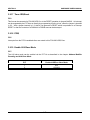
SYS68K/CPU-40/41
User’s Manual
Edition No. 8
February 1997
P/N 202368
FORCE COMPUTERS Inc./GmbH
All Rights Reserved
This document shall not be duplicated, nor its contents used
for any purpose, unless express permission has been granted.
Copyright by FORCE COMPUTERS
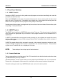
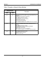
INTRODUCTION
This page was intentionally left blank
TABLE OF CONTENTS
1.
GENERAL INFORMATION . . . . . . . . . . . . . . . . . . . . . . . . . . . . . . . . . . . . . . . . . . .
1-1
1.1
Features of the CPU Board . . . . . . . . . . . . . . . . . . . . . . . . . . . . . . . . . . . . . . . . . . .
1-4
2.
THE PROCESSOR . . . . . . . . . . . . . . . . . . . . . . . . . . . . . . . . . . . . . . . . . . . . . . . . .
2-1
2.1
The CPU 68040 . . . . . . . . . . . . . . . . . . . . . . . . . . . . . . . . . . . . . . . . . . . . . . . . . . .
2-1
2.2
2.2.1
2.2.2
2.2.3
2.2.4
The Shared RAM . . . . . . . . . . . . . . . . . . . . . . . . . . . . . . . . . . . . . . . . . . . . . . . . . .
The DRM-01/4 . . . . . . . . . . . . . . . . . . . . . . . . . . . . . . . . . . . . . . . . . . . . . . . . . . . . .
The DRM-01/16 . . . . . . . . . . . . . . . . . . . . . . . . . . . . . . . . . . . . . . . . . . . . . . . . . . . .
The SRM-01/4 . . . . . . . . . . . . . . . . . . . . . . . . . . . . . . . . . . . . . . . . . . . . . . . . . . . . .
The SRM-01/8 . . . . . . . . . . . . . . . . . . . . . . . . . . . . . . . . . . . . . . . . . . . . . . . . . . . . .
2-3
2-3
2-4
2-5
2-6
2.3
The System EPROM . . . . . . . . . . . . . . . . . . . . . . . . . . . . . . . . . . . . . . . . . . . . . . . .
2-7
2.4
The Local SRAM . . . . . . . . . . . . . . . . . . . . . . . . . . . . . . . . . . . . . . . . . . . . . . . . . . .
2-7
2.5
The Local FLASH EPROM . . . . . . . . . . . . . . . . . . . . . . . . . . . . . . . . . . . . . . . . . . .
2-7
2.6
The Boot EPROM . . . . . . . . . . . . . . . . . . . . . . . . . . . . . . . . . . . . . . . . . . . . . . . . . .
2-7
2.7
The FGA-002 . . . . . . . . . . . . . . . . . . . . . . . . . . . . . . . . . . . . . . . . . . . . . . . . . . . . .
2-8
2.8
2.8.1
2.8.2
The PI/T 68230 . . . . . . . . . . . . . . . . . . . . . . . . . . . . . . . . . . . . . . . . . . . . . . . . . . . . 2-9
The I/O Configuration of PI/T1 . . . . . . . . . . . . . . . . . . . . . . . . . . . . . . . . . . . . . . . . 2-10
The I/O Configuration of PI/T2 . . . . . . . . . . . . . . . . . . . . . . . . . . . . . . . . . . . . . . . . 2-10
2.9
The Real Time Clock 72423 . . . . . . . . . . . . . . . . . . . . . . . . . . . . . . . . . . . . . . . . .
2-11
2.10
2.10.1
The DUSCC 68562 . . . . . . . . . . . . . . . . . . . . . . . . . . . . . . . . . . . . . . . . . . . . . . . .
The I/O Configuration of DUSCC1 and DUSCC2 . . . . . . . . . . . . . . . . . . . . . . . . . .
2-12
2-13
2.11
The EAGLE Modules . . . . . . . . . . . . . . . . . . . . . . . . . . . . . . . . . . . . . . . . . . . . . . .
2-15
2.12
The VMEbus Interface . . . . . . . . . . . . . . . . . . . . . . . . . . . . . . . . . . . . . . . . . . . . . .
2-15
2.13
The Monitor of the CPU board . . . . . . . . . . . . . . . . . . . . . . . . . . . . . . . . . . . . . . . .
2-17
2.14
Default Jumper Settings on the CPU Board . . . . . . . . . . . . . . . . . . . . . . . . . . . . . .
2-18
3.
SPECIFICATIONS OF THE CPU BOARD . . . . . . . . . . . . . . . . . . . . . . . . . . . . . . . .
3-1
4.
ORDERING INFORMATION . . . . . . . . . . . . . . . . . . . . . . . . . . . . . . . . . . . . . . . . . .
4-1
5.
HISTORY OF MANUAL REVISIONS . . . . . . . . . . . . . . . . . . . . . . . . . . . . . . . . . . . .
5-1
i
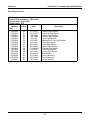
LIST OF FIGURES
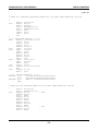
Figure 1-1:
Figure 1-2:
Figure 2-1:
Figure 2-2:
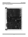
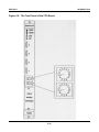
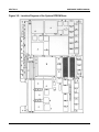
Photo of the CPU Board . . . . . . . . . . . . . . . . . . . . . . . . . . . . . . . . . . . . . . . . . . . . . 1-2
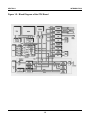
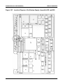
Block Diagram of the CPU Board . . . . . . . . . . . . . . . . . . . . . . . . . . . . . . . . . . . . . . 1-3
Location Diagram for All Jumperfields . . . . . . . . . . . . . . . . . . . . . . . . . . . . . . . . . 2-20
The Front Panel of the CPU Board . . . . . . . . . . . . . . . . . . . . . . . . . . . . . . . . . . . . 2-21
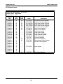
LIST OF TABLES
Table 1-1:
Table 1-2:
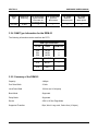
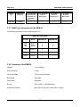
The Memory Map . . . . . . . . . . . . . . . . . . . . . . . . . . . . . . . . . . . . . . . . . . . . . . . . . .
The Base Addresses of the Local I/O Devices . . . . . . . . . . . . . . . . . . . . . . . . . . . . .
ii
1-6
1-7
This page was intentionally left blank
iii
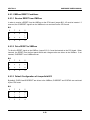
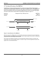
SECTION 1
INTRODUCTION
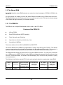
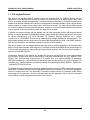
1. GENERAL INFORMATION
This CPU board is a high performance single board computer based on the 68040 microprocessor and the
VMEbus. The board incorporates a modular I/O subsystem which provides a high degree of flexibility for
a wide variety of applications. The CPU board can be used with or without an I/O subsystem, called an
"EAGLE" module.
The board is able to hold a RAM Module which can be DRAM (CPU-40) or SRAM (CPU-41) based.
The CPU-40/41 family design utilizes all of the features of the powerful FORCE Gate Array (FGA-002).
Among its features is a 32-bit DMA controller which supports local (shared) memory, VMEbus and I/O data
transfers for maximum performance, parallel real time operation and responsiveness.
The EAGLE modules are installed on the CPU board via the FLXi (FORCE Local eXpansion interface). This
provides a full 32-bit interface between the base board and the EAGLE module I/O subsystem, providing
a range of I/O options.
Four multiprotocol serial I/O channels, a parallel I/O channel and a Real Time Clock with on-board battery
backup are installed on the base board which, in combination with EAGLE modules, make the CPU board
a true single board computer system.
A broad range of operating systems and kernels is available for the CPU board. However, as with all
FORCE COMPUTERS' CPU cards, VMEPROM firmware is provided with the board at no extra cost.
VMEPROM is a Real Time Kernel and is installed on the CPU board in the two 16-bit wide EPROM sockets,
which results in a 32-bit wide System EPROM area. This ensures that the board is supplied ready to use.
1-1
SYS68K/CPU-40/41 USER'S MANUAL
FORCE COMPUTERS
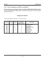
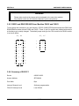
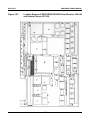
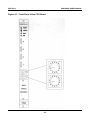
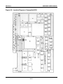
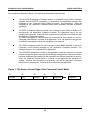
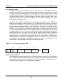
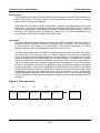
Figure 1-1: Photo of the CPU Board
1-2
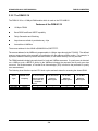
SECTION 1
INTRODUCTION
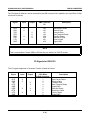
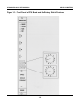
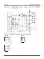
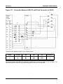
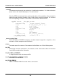
Figure 1-2: Block Diagram of the CPU Board
1-3
SYS68K/CPU-40/41 USER'S MANUAL
FORCE COMPUTERS
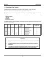
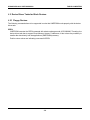
1.1 Features of the CPU 3Board
!
68040 microprocessor:
25.0 MHz on CPU-40B/41B/x
!
68040 microprocessor:
33.0 MHz on CPU-40D/41D/x
!
Shared DRAM Module:
4 Mbyte DRAM with Burst Read/Write and Parity Generation and
Checking (DRM-01/4)
16 Mbyte DRAM with Burst Read/Write and Parity Generation and
Checking (DRM-01/16)
!
Shared SRAM Module:
4 Mbyte SRAM with Burst Read/Write (SRM-01/4)
8 Mbyte SRAM with Burst Read/Write (SRM-01/8)
!
!
32-bit high speed DMA controller for data transfers to/from the shared RAM, VMEbus memory and
EAGLE modules; DMA controller is installed in the FGA-002.
Two system EPROM devices supporting 40-pin devices. Access from the 68040 using a 32-bit data
path
!
One boot EPROM for local booting, initialization of the I/O chips and configuration of the FGA-002
!
128 Kbyte SRAM with on-board battery backup
!
128 Kbyte FLASH EPROM
!
FLXi interface for installation of one EAGLE module
!
Four Serial I/O interfaces, configurable as RS232/RS422/RS485, available on the front panel
!
8-bit parallel interface with 4-bit handshake
!
Two 24-bit timers with 5-bit prescaler
!
One 8-bit timer
!
Real Time Clock with calendar and on-board battery backup
!
Full 32-bit VMEbus master/slave interface, supporting the following data transfer types:
#
#
#
!
A32, A24, A16 : D8, D16, D32 - Master
A32, A24 : D8, D16, D32 - Slave
UAT, RMW, ADO
FORCE Message Broadcast (FMB), two channels
1-4
SECTION 1
INTRODUCTION
Features of the CPU Board (cont'd)
!
Four-level VMEbus arbiter
!
SYSCLK driver
!
VMEbus interrupter (IR 1-7)
!
VMEbus interrupt handler (IH 1-7)
!
Support for ACFAIL* and SYSFAIL
!
Bus timeout counters for local and VMEbus access (15 µsec)
!
VMEPROM, Real Time Multitasking Kernel with monitor, file manager and debugger
1-5
SYS68K/CPU-40/41 USER'S MANUAL
FORCE COMPUTERS
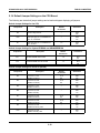
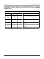
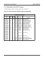
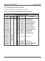
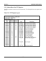
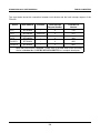
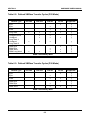
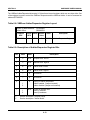
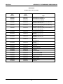
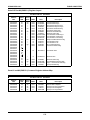
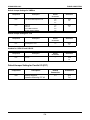
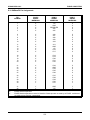
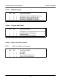
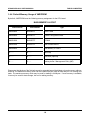
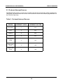
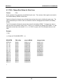
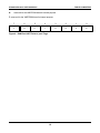
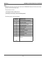
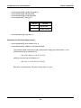
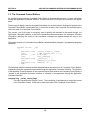
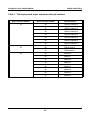
The following table summarizes the memory map of the CPU board.
Table 1-1: The Memory Map
Start
Address
End
Address
00000000
00000000
00000000
003FFFFF
007FFFFF
00FFFFFF
Shared Memory (4 Mbyte)
Shared Memory (8 Mbyte) or
Shared Memory (16 Mbyte)
00400000
F9FFFFFF
VMEbus Addresses (4 Mbyte Shared Memory)
A32: D32, D24, D16, D8
00800000
F9FFFFFF
VMEbus Addresses (8 Mbyte Shared Memory)
A32: D32, D24, D16, D8
01000000
F9FFFFFF
VMEbus Addresses (16 Mbyte Shared Memory)
A32: D32, D24, D16, D8
FA000000
FAFFFFFF
Message Broadcast Area
FB000000
FBFEFFFF
VMEbus
A24: D32, D24, D16, D8
FBFF0000
FBFFFFFF
VMEbus
A16: D32, D24, D16, D8
FC000000
FCFEFFFF
VMEbus
A24: D16, D8
FCFF0000
FCFFFFFF
VMEbus
A16: D16, D8
FD000000
FEFFFFFF
Reserved
FF000000
FF7FFFFF
SYSTEM EPROM
FF800000
FFBFFFFF
Local I/O
FFC00000
FFC7FFFF
LOCAL SRAM
FFC80000
FFCFFFFF
Local FLASH EPROM
FFD00000
FFDFFFFF
Registers of FGA-002
FFE00000
FFEFFFFF
BOOT EPROM
FF803E00
FF803FFF
VMEbus Arbiter
FFF00000
FFFFFFFF
Reserved
Type
1-6
SECTION 1
INTRODUCTION
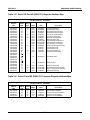
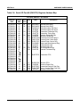
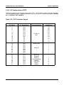
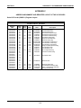
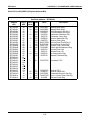
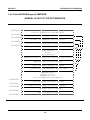
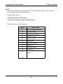
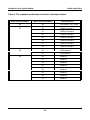
This table gives a brief overview of the local I/O devices and the equivalent base address.
Table 1-2: The Base Addresses of the Local I/O Devices
BASE ADDRESS
$FF803000
$FF802000
$FF802200
$FF800C00
$FF800E00
DEVICE
RTC
DUSCC1
DUSCC2
PI/T1
PI/T2
1-7
72423
68562
68562
68230
68230
SECTION 1
INTRODUCTION
2. THE PROCESSOR
2.1 The CPU 68040
The 68040 is a third generation full 32 bit enhanced microprocessor. The 68040 is upward object code
compatible with the 68030, 68020, 68010 and 68000 line of microprocessors.
The 68040 combines a central processing unit core, an instruction cache, a data cache, a memory
management unit, and an enhanced bus controller.
This virtual memory processor utilizes multiple, concurrent execution units and a highly integrated
architecture providing a high level of performance.
The 68040 processor combines a 68030 compatible integer unit, a 68881/68882 compatible floating point
unit (FPU), memory management units (MMUs), and a 4 Kbyte instruction and data cache. Cache
functionality is strengthened by the built-in on-chip bus snooping logic which instantly supports cache logic
during multimaster applications.
Instruction administration is routed through both the integer unit and FPU, which link to the fully independent
data and instruction memory units. Each memory unit consists of an MMU, an address translation cache
(ATC), a main cache, and a snoop controller.
The internal blocks are designed to operate in parallel, allowing instruction execution to be overlapped. In
addition, the internal caches, the on-chip memory management unit, and the enhanced bus controller
operate parallel to one another.
The 68040 contains an enhanced bus controller that supports both synchronous/ asynchronous bus cycles
and burst data transfers. It contains a nonmultiplexed address bus and data bus and supports 32 bits of
address and data.
2-1
SYS68K/CPU-40/41 USER'S MANUAL
FORCE COMPUTERS
Features of the 68040
!
Nonmultiplexed 32 bit address and data buses
!
16 general purpose address and data registers (32 bit wide)
!
8 floating point data registers (80 bit wide)
!
Two supervisor stack pointers (32 bit wide)
!
19 special purpose control registers
!
4 Kbyte instruction and 4 Kbyte data cache
!
On-chip paged memory management unit
!
Pipelined architecture with parallelism allowing accesses to internal caches, bus transfers, and
instruction execution in parallel
!
Synchronous bus cycles and burst read and write data transfers
!
Complete floating point support given to the 68882 FPCP subset and software emulation
!
68030 compatible
!
Low latency bus accesses to reduce cache miss penalty
!
Maximized throughput from the integer unit, FPU, MMU and bus controller
!
4 Gbyte direct addressing range
2-2
SECTION 1
INTRODUCTION
2.2 The Shared RAM
On this CPU board the shared RAM is placed on a module to allow the adaption of DRAM or SRAM to the
base board.
All signals which are needed to control the shared RAM are available on the RAM module connector.
Therefore RAM devices with different access times can also be used on this CPU board to take advantage
of the 68040 with higher frequency if it becomes available.
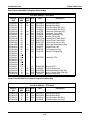
2.2.1 The DRM-01/4
The DRM-01/4 is a 4 Mbyte RAM module which is used on the CPU-40B/4.
Features of the DRM-01/4
!
4 Mbyte DRAM
!
Burst READ and Burst WRITE capability
!
Parity Generation and Checking
!
Asynchronous refresh is provided every 14µs
!
Accessible via VMEbus
The access address for the 68040 is $00000000 to $003FFFFF.
The access address for the VMEbus is programmable in 4 Kbyte steps through the FGA-002. The defined
memory range can be write protected in coordination with the address modifier codes. For example, in
supervisor mode the memory can be read and written, in user mode memory can only be read.
The DRAM module includes byte parity check for local and VMEbus accesses. If a parity error is detected
on a VMEbus cycle, a BERR is forced to the VMEbus informing the requestor that a parity error has
occurred. On local accesses, a Transfer Error Acknowledge (TEA) is forced to the processor if a parity
error was detected.
The following chart lists the required CPU clock cycles and wait states for accessing the shared RAM.
Board
Type
68040 Clock
Frequency
No. of CPU Clock
Cycles Counted
From TS to TA
for Normal Cycles
No. of CPU Clock
Cycles for
Burst Cycles
No. of Wait
States for
Normal Cycles
No. of Wait
States for
Burst Cycles
CPU-40/B
25 MHz
4
1
3
0
2-3
SYS68K/CPU-40/41 USER'S MANUAL
FORCE COMPUTERS
2.2.2 The DRM-01/16
The DRM-01/16 is a 16 Mbyte RAM module which is used on the CPU-40B/16.
Features of the DRM-01/16
!
16 Mbyte DRAM
!
Burst READ and Burst WRITE capability
!
Parity Generation and Checking
!
Asynchronous refresh is provided every 14µs
!
Accessible via VMEbus
The access address for the 68040 is $00000000 to $00FFFFFF.
The access address for the VMEbus is programmable in 4 Kbyte steps through the FGA-002. The defined
memory range can be write protected in coordination with the address modifier codes. For example, in
supervisor mode the memory can be read and written, in user mode memory can only be read.
The DRAM module includes byte parity check for local and VMEbus accesses. If a parity error is detected
on a VMEbus cycle, a BERR is forced to the VMEbus informing the requestor that a parity error has
occurred. On local accesses, a Transfer Error Acknowledge (TEA) is forced to the processor if a parity
error was detected.
The following chart lists the required CPU clock cycles and wait states for accessing the shared RAM.
Board
Type
68040-B Clock
Frequency
No. of CPU Clock
Cycles Counted
From TS to TA
for Normal
Cycles
No. of CPU Clock
Cycles for
Burst Cycles
No. of Wait
States for
Normal Cycles
No. of Wait
States for
Burst Cycles
CPU-40/B
25 MHz
4
1
3
0
2-4
SECTION 1
INTRODUCTION
2.2.3 The SRM-01/4
The SRM-01/4 is a 4 Mbyte RAM module which is used on the CPU-41B/4.
Features of the SRM-01/4
!
4 Mbyte SRAM
!
Burst READ and Burst WRITE capability
!
Battery Backup via VMEbus
!
Accessible via VMEbus
The access address for the 68040 is $00000000 to $003FFFFF.
The access address for the VMEbus is programmable in 4 Kbyte steps through the FGA-002. The defined
memory range can be write protected in coordination with the address modifier codes. For example, in
supervisor mode the memory can be read and written, in user mode memory can only be read.
Parity check is not necessary for SRAM devices, because these components are protected against soft
errors owing alpha emission. The following chart lists the required CPU clock cycles and wait states for
accessing the shared RAM.
Board
Type
68040 Clock
Frequency
No. of CPU Clock
Cycles Counted
From TS to TA
for Normal Cycles
No. of CPU Clock
Cycles for
Burst Cycles
No. of Wait
States for
Normal Cycles
No. of Wait
States for
Burst Cycles
CPU-41/B
25 MHz
3
1
2
0
2-5
SYS68K/CPU-40/41 USER'S MANUAL
FORCE COMPUTERS
2.2.4 The SRM-01/8
The SRM-01/8 is an 8 Mbyte RAM module which is used on the CPU-41B/8.
Features of the SRM-01/8
!
8 Mbyte SRAM
!
Burst READ and Burst WRITE capability
!
Battery Backup via VMEbus
!
Accessible via VMEbus
The access address for the 68040 is $00000000 to $007FFFFF.
The access address for the VMEbus is programmable in 4 Kbyte steps through the FGA-002. The defined
memory range can be write protected in coordination with the address modifier codes.
For example, in supervisor mode the memory can be read and written, in user mode memory can only be
read.
Parity check is not necessary for SRAM devices, because these components are protected against soft
errors owing alpha emission. The following chart lists the required CPU clock cycles and wait states for
accessing the shared RAM.
Board
Type
68040 Clock
Frequency
No. of CPU Clock
Cycles Counted
From TS to TA
for Normal
Cycles
No. of CPU Clock
Cycles for
Burst Cycles
No. of Wait
States for
Normal Cycles
No. of Wait
States for
Burst Cycles
CPU-41/B
25 MHz
3
1
2
0
2-6
SECTION 1
INTRODUCTION
2.3 The System EPROM
The CPU board offers two 40-pin EPROM sockets for the installation of two 16-bit wide EPROM devices.
The EPROMs present a full 32-bit data path to the processor enabling maximum performance. The
following devices are supported in the system EPROM area:
Supported Device Types in the System EPROM Area:
Organization
Total Memory Capacity
64K x 16
128K x 16
256K x 16
512K x 16
256 Kbytes
512 Kbytes
1 Mbyte
2 Mbytes
2.4 The Local SRAM
The CPU board contains a 128K * 8 bit SRAM. Battery backup is provided via the on-board battery or the
VMEbus +5VSTDBY line.
2.5 The Local FLASH EPROM
A 128 Kbyte FLASH EPROM is included on the base board of the CPU-40 which can be used as additional
data backup under conditions of power down for long periods. FLASH EPROM is ideal to hold details of
the board status, such as software revision or user data which is to be kept permanently.
2.6 The Boot EPROM
The CPU board contains, in addition to the two system EPROMs, a single boot EPROM to boot the local
microprocessor, initialize all I/O devices and program the board-dependent functions of the FGA-002. All
basic initialization of the I/O devices and the FGA-002 are made through the boot EPROM.
In addition, the boot EPROM contains user utility routines, which may be called out of the user's application
program. These routines provide easy software access to the functionality of the FGA-002 (DMA controller,
FORCE Message Broadcast, Interrupt Management, etc.).
2-7
SYS68K/CPU-40/41 USER'S MANUAL
FORCE COMPUTERS
2.7 The FGA-002
One of the main features on this CPU board is the FGA-002 Gate Array with 24,000 gates and 281 pins.
The FGA-002 controls the local bus and builds the VMEbus interface. It also includes a DMA controller,
a complete interrupt handler, message broadcast interface (FMB), timer functions, mailbox locations, and
a VMEbus interrupter. This gate array monitors the local bus, which in turn signifies that if any local I/O
device is to be accessed, the gate array overrules all control signals, used address signals, and data
signals.
The FGA-002 serves as a VMEbus manager. All VMEbus address and data lines are connected to the
gate array through the buffers. Additional functions such as the VMEbus interrupt handler are also installed
on the FGA-002. The on-chip DMA controller can access the local memory, VMEbus memory, and onboard devices which are able to function in a DMA mode. The start address of the FGA-002 registers is
$FFD00000. All registers of the gate array and associated functions are described in detail in the FGA-002
Users Manual. On the following page you will find a list of features for the FGA-002.
Features of the FGA-002
!
32 bit DMA Controller
!
2 Message Broadcast Channels (FMB)
!
8 Mailbox Interrupt Channels
!
One 8 bit timer
!
Complete Interrupt Management for VMEbus interrupts, ACFAIL, SYSFAIL, Onboard Interrupts and
FGA-002 internal interrupts
!
VMEbus interface including a single level arbiter
!
Decoding logic for accesses to the Shared Memory of the CPU board
A complete functional description of the FGA-002 may be found in the FGA-002 Users Manual.
2-8
SECTION 1
INTRODUCTION
2.8 The PI/T 68230
The MC68230 Parallel Interface/Timer (PI/T) provides versatile double buffered parallel interfaces and an
operating system oriented timer for MC68000 systems. The parallel interfaces operate in unidirectional or
bidirectional modes, 8 or 16 bits wide. The PI/T timer contains a 24 bit wide counter and a 5 bit prescaler.
Features of the PI/T
!
!
MC68000 Bus Compatible
Port Modes Include: Bit I/O
Unidirectional 8 bit and 16 bit
Bidirectional 8 bit and 16 bit
!
Selectable Handshaking Options
!
24 bit Programmable Timer
!
Software Programmable Timer Modes
!
Contains Interrupt Vector Generation Logic
!
Separate Port and Timer Interrupt Service Requests
!
Registers are Read/Write and Directly Addressable
2-9
SYS68K/CPU-40/41 USER'S MANUAL
FORCE COMPUTERS
2.8.1 The I/O Configuration of PI/T1
Port A is connected to the two 4 bit HEX rotary switches provided on the front panel for application
dependent settings.
Port B is used for programming the local base address for A24 accesses from the VMEbus.
Port C is used for port and timer interrupts and to control the RMC behavior of the board.
2.8.2 The I/O Configuration of PI/T2
Port A and the handshake lines are routed to a 24-pin header which allows the connection of a flat cable.
8 bits are connected to port A of the PI/T and can be used as inputs or outputs, with the remaining 4 bits
being connected to the handshake pins of the PI/T. This port can be used to establish a "Centronics type"
interface.
Port B allows the memory capacity of the Shared RAM to be read. Each CPU board of this type contains
three readable status bits describing the memory capacity. In addition, the CPU board type can be read
through the remaining 5 bits.
Port C grants the RAM type (DRAM/SRAM) burst and parity capability of the Shared RAM to be read.
A "Powerup Reset" can be initiated by software.
2-10
SECTION 1
INTRODUCTION
2.9 The Real Time Clock 72423
There is a Real Time Clock (RTC) 72423 installed on the CPU board. The CPU board contains a self
supportive battery to sustain the RTC during power down.
Features of the RTC
!
Built-in quartz oscillator makes regulation unnecessary and allows easy design
!
Direct bus compatibility (120 ns access time)
!
Incorporated built-in time (hour, minute, second), and date (year, month, week, day) counters
!
12 hour and 24 hour clock switchover functions and automatic leap year setting
!
Interrupt masking
!
An error adjustment time function of 30 seconds
!
READ, WRITE, HOLD, STOP, RESET, and CHIP SELECT inputs
!
The C-MOS IC boasts low current consumption and features a backup function
!
A 24-pin so package
2-11
SYS68K/CPU-40/41 USER'S MANUAL
FORCE COMPUTERS
2.10 The DUSCC 68562
The Dual Universal Serial Communications Controller (DUSCC) 68562 is installed to communicate with
terminals, computers, or other equipment.
The DUSCC is a single chip MOS-LSI communications device providing two independent, multiprotocol,
full duplex receiver/transmitter channels in a single package. Each channel consists of a receiver,
transmitter, 16-bit multifunction counter/timer, digital phaselocked loop (DPLL), parity/CRC generator and
checker, and associated control circuits.
Features of the DUSCC
!
Dual full duplex synchronous/asynchronous receiver and transmitter
!
Multiprotocol operation consisting of:
BOP:
COP:
ASYNC:
HDLC/ADCCP, SDLC, SDLC Loop, X.25 or X.75 link level
BISYNC, DDCMP, X.21
5-8 bit plus optional parity
!
Programmable data encoding formats: NRZ, NRZI, FM0, FM1, Manchester
!
4 character receiver and transmitter FIFOs
!
Individual programmable baud rate for each receiver and transmitter
!
Digital phase locked loop
!
User programmable counter/timer
!
Programmable channel modes full/half duplex, auto echo, local loopback
!
Modem control signals for each channel: RTS, CTS, DCD
!
CTS and DCD programmable autoenables for Receiver (RX) and Transmitter (TX)
!
Programmable interrupt on change of CTS or DCD
2-12
SECTION 1
INTRODUCTION
2.10.1 The I/O Configuration of DUSCC1 and DUSCC2
The four channels may be configured to function as a RS232 or RS422/RS485 compatible interface.
Termination resistors can be installed to adapt various cable lengths and reduce reflections upon the
selection of the RS422/RS485 compatible interface. The DUSCC can interrupt the local CPU at a specified
programmable IRQ level.
I/O Signals for DUSCC1:
The I/O signal assignment of channel 1 to 2 is listed as follows:
Signal
Input
DCD
RXD
TXD
DTR
GND
DSR
RTS
CTS
GND
X
X
Output
X
X
X
X
X
X
9 Pin Micro
D-Sub Connector
1
2
3
4
5
6
7
8
9
2-13
Description
Data Carrier Detect
Receive Data
Transmit Data
Data Terminal Ready
Signal GND
Data Set Ready
Request to Send
Clear to Send
Signal GND
SYS68K/CPU-40/41 USER'S MANUAL
FORCE COMPUTERS
The I/O signals of channel 1 can be connected to the VME connector P2 in parallel to the 9-pin Micro D-Sub
connector as follows:
Signal
Input
DCD
RXD
TXD
DTR
DSR
RTS
CTS
GND
X
X
Output
X
X
X
X
X
X
VME Connector
P2
c29
c30
c31
c32
a29
a30
a31
a32
Description
Data Carrier Detect
Receive Data
Transmit Data
Data Terminal Ready
Data Set Ready
Request to Send
Clear to Send
Signal GND
NOTE
This is only possible if these VMEbus P2 lines are not used by an EAGLE module.
I/O Signals for DUSCC2:
The I/O signal assignment of channels 3 and 4 is listed as follows:
Signal
Input
DCD
RXD
TXD
DTR
GND
DSR
RTS
CTS
GND
X
X
Output
X
X
X
X
X
X
9 Pin Micro
D-Sub Connector
1
2
3
4
5
6
7
8
9
2-14
Description
Data Carrier Detect
Receive Data
Transmit Data
Data Terminal Ready
Signal GND
Data Set Ready
Request to Send
Clear to Send
Signal GND
SECTION 1
INTRODUCTION
2.11 The EAGLE Modules
EAGLE modules are I/O subsystems designed not only to increase the functionality of the board but to add
the exact I/O features to fit the application requirement. EAGLE modules connect directly onto the FLXi
of the base board. FLXi and EAGLE modules will be a feature on future FORCE board generations to
ensure continued flexibility.
If your CPU board is assembled with an EAGLE module please refer to the "EAGLE Module" manual which
is shipped with this board and should be placed in Section 6 of this manual.
2.12 The VMEbus Interface
The CPU board has a full 32-bit VMEbus interface. The address modifier codes for A16, A24 and A32
addressing are fully supported in master mode. In slave mode, the address modifiers for A32 and A24 are
fully supported.
Read-Modify-Write cycles are fully supported to allow multiple CPU boards to be synchronized via the
shared RAM. The FGA-002 determines whether or not an access to the shared RAM is allowed and, if
allowed, controls the access cycle.
The CPU board provides an interrupt handler capability (IH 1-7) which can be enabled/disabled by
programming the FGA-002. The CPU board also provides an interrupter function which enables the board
to send interrupts to the
VMEbus on seven programmable levels with a software-programmable vector.
The following bus release modes are supported:
RWD
ROR
RBCLR
RAT
REC
ROACF
=
=
=
=
=
=
Release When Done
Release On Request
Release On Bus Clear
Release After Timeout
Release Every Cycle
Release On ACFAIL*
2-15
SYS68K/CPU-40/41 USER'S MANUAL
FORCE COMPUTERS
Each of the listed modes is software programmable inside the gate array. The bus request level of the CPU
board is jumper or software selectable (BRO-3).
The DMA controller installed in the FGA-002 on the CPU board is able to access the VMEbus interface
independently from the microprocessor, enabling VMEbus communication to take place without impacting
the processing capabilities of the rest of the board for number crunching or servicing on-board I/O.
A four level arbiter with round robin and prioritized round robin arbitration modes, a power monitor, a
SYSRESET* generator, IACK* daisy chain driver and support for ACFAIL*, SYSFAIL* and SYSCLK
complete the VMEbus interface.
2-16
SECTION 1
INTRODUCTION
2.13 The Monitor of the CPU board
Every CPU board contains VMEPROM, a real time multitasking monitor debugger. It consists of a powerful
real time kernel, file manager and monitor/debugger with 68040 line assembler/disassembler.
The monitor/debugger includes all functions to control the real time kernel and file manager as well as all
tools required for program debugging such as breakpoints, tracing, memory display, memory modify and
host communication.
VMEPROM supports several memory and I/O boards on the VMEbus to take full advantage of the file
manager and kernel functions.
A built-in selftest checks all on-board devices and memory. This allows detection of any failures on the
board.
Memory initialization and test commands offer easy installation of global memory in the environment on the
local RAM and/or the VMEbus.
The one line assembler/disassembler is 68040 compatible and supports all 68040 commands in the original
mnemonic described in the MC 68040 User's Manual.
2-17
SYS68K/CPU-40/41 USER'S MANUAL
FORCE COMPUTERS
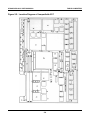
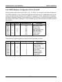
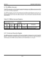
2.14 Default Jumper Settings on the CPU Board
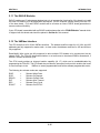
The following are the default jumper settings and a location diagram displaying all jumpers.
Default Jumper Settings for the CPU
Jumperfield
Description
Default
Connection
Schematics
B2
Reset Voltage Sensor
---
SH4
B4
B20
Backup Supply for Local SRAM and
RTC via +5VSTDBY
---
SH4
B2
B1
Backup Supply for Local SRAM and
RTC via Bat 1
1-2
SH4
B2
Default Jumper Settings for System EPROMs and SRAM/EEPROM
Jumperfield
Description
Default
Connection
Schematics
B11
System EPROM device select
1-6
SH5
A4
B16
FLASH EPROM write dis-/enable
1-2
SH4
C2
Default Jumper Settings for Serial I/O (RS232)
Jumperfield
Description
Default
Connection
Schematics
B3
Connector 1, PD1
(DUSCC1 Port #1)
2-15
8-9
SH6
B2
B4
Connector 2, PD2
(DUSCC1 Port #2)
2-15
8-9
SH6
B3
B5
Connector 1, PD1
(DUSCC1 Port #1)
---
SH6
C2
B6
Connector 2, PD2
(DUSCC Port #2)
---
SH6
C3
B7
Connector 3, PD3
(DUSCC2 Port #3)
2-15
8-9
SH7
B2
B8
Connector 4, PD4
(DUSCC2 Port #4)
2-15
8-9
SH7
B3
B9
Connector 3, PD3
(DUSCC2 Port #3), PD3
---
SH7
C2
B10
Connector 4, PD4
(DUSCC Port #4), PD4
---
SH7
C3
2-18
SECTION 1
INTRODUCTION
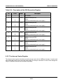
Default Jumper Settings for VMEbus
Jumperfield
Description
Default
Connection
Schematics
B19
Four level Arbiter Request Level
1-6
2-5
3-4
SH9
B4
B13
SYSCLK
SYSFAIL
Receive VMEbus RESET
Drive VMEbus RESET
1-8
2-7
3-6
4-5
SH10
C2
Default
Connection
Schematics
1-2
SH16
A1
Default
Connection
Schematics
---
SH8
D1
Default
Connection
Schematics
2-3
SH8
D4
Default Jumper Settings for Test
Jumperfield
B17
Description
Clock Signal to CPU
Headers for 12 Bit I/O and 8 Bit I/O
Jumperfield
B12
Description
User I/O
Default Jumper Setting for Parallel I/O (PI/T)
Jumperfield
B18
Description
Interrupt Request,
Hardware Watchdog PI/T #2
2-19
SYS68K/CPU-40/41 USER'S MANUAL
FORCE COMPUTERS
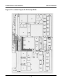
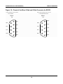
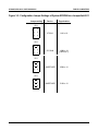
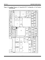
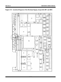
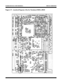
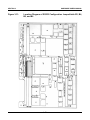
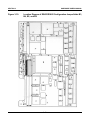
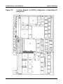
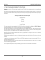
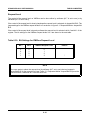
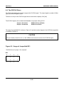
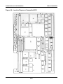
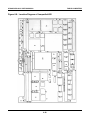
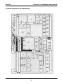
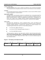
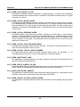
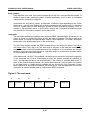
Figure 2-1: Location Diagram for All Jumperfields
2-20
SECTION 1
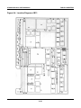
INTRODUCTION
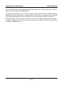
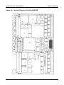
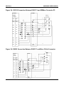
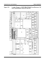
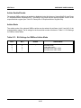
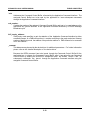
Figure 2-2: The Front Panel of the CPU Board
2-21
SYS68K/CPU-40/41 USER'S MANUAL
FORCE COMPUTERS
This page intentionally left blank
2-22
SECTION 1
INTRODUCTION
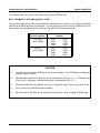
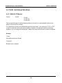
3. SPECIFICATIONS OF THE CPU BOARD
CPU Type
68040
CPU Clock Frequency
CPU-40B/x
CPU-40D/x
25.0 MHz
33.0 MHz
Shared DRAM Capacity with Parity
CPU-40X/4
CPU-40X/16
4 Mbytes
16 Mbytes
Shared SRAM Capacity
CPU-41X/4
CPU-41X/8
4 Mbytes
8 Mbytes
SRAM Capacity with On-board Battery Backup
FLASH EPROM
128 Kbytes
128 Kbytes
Number of System EPROM Sockets
Data Path
2
32-Bits
Serial I/O Interfaces (68562)
RS232/RS422/RS485 Compatible
4
4 of 4
24-bit Timer with 5-bit Prescaler
8-bit Timer
2
1
Parallel I/O Interface (68230)
12 Lines
Real Time Clock with On-board Battery Backup
72423
VMEbus Interface
Master
Slave
A32, A24, A16:D8, D16, D32, UAT, RMW
A32, A24:D8, D16, D32, RMW
Four Level Arbiter
SYSCLK Driver
Mailbox Interrupts
Yes
Yes
8
FORCE Message Broadcast
FMB FIFO 0
FMB FIFO 1
8 Bytes
1 Byte
VMEbus Interrupter/VMEbus and Local Interrupt Handler
All Sources can be Routed to a Software Programmable IRQ Level
1 to 7
Yes
RESET/ABORT Switch
Yes
VMEPROM Firmware Installed on All Board Versions
256 Kbytes
Power Requirements
+5V min/max
+12V min/max
-12V min/max
5.2A/6.0A
0.1A/0.3A
0.1A/0.3A
0 to +50EC
-40 to +85EC
0 to 95%
234x160mm/9.2x6.3in
1
Operating Temperature with Forced Air Cooling
Storage Temperature
Relative Humidity (noncondensing)
Board Dimensions
No. of Slots Used
3-1
SYS68K/CPU-40/41 USER'S MANUAL
FORCE COMPUTERS
This page intentionally left blank
3-2
SECTION 1
INTRODUCTION
4. ORDERING INFORMATION
SYS68K/CPU-40B/4-00
25.0 MHz 68040 based CPU board with DMA, 4 Mbyte shared DRAM, 4 serial I/O channels,
FLXi, VMEPROM. Documentation included.
SYS68K/CPU-40B/4-01
25.0 MHz 68040 based CPU board with DMA, 4 Mbyte shared DRAM, 4 serial I/O channels,
EAGLE-01C (SCSI, floppy disk and Ethernet Interface), VMEPROM. Documentation included.
SYS68K/CPU-40B/16-00
25.0 MHz 68040 based CPU board with DMA, 16 Mbyte shared DRAM, 4 serial I/O channels,
FLXi, VMEPROM. Documentation included.
SYS68K/CPU-40B/16-01
25.0 MHz 68040 based CPU board with DMA, 16 Mbyte shared DRAM, 4 serial I/O channels,
EAGLE-01C (SCSI, floppy disk and Ethernet Interface), VMEPROM. Documentation included.
SYS68K/CPU-40D/4-00
33.0 MHz 68040 based CPU board with DMA, 4 Mbyte shared DRAM, 4 serial I/O channels,
FLXi, VMEPROM. Documentation included.
SYS68K/CPU-40D/4-01
33.0 MHz 68040 based CPU board with DMA, 4 Mbyte shared DRAM, 4 serial I/O channels,
EAGLE-01C (SCSI, floppy disk and Ethernet Interface), VMEPROM. Documentation included.
SYS68K/CPU-40D/16-00
33.0 MHz 68040 based CPU board with DMA, 16 Mbyte shared DRAM, 4 serial I/O channels,
FLXi, VMEPROM. Documentation included.
SYS68K/CPU-40D/16-01
33.0 MHz 68040 based CPU board with DMA, 16 Mbyte shared DRAM, 4 serial I/O channels,
EAGLE-01C (SCSI, floppy disk and Ethernet Interface), VMEPROM. Documentation included.
SYS68K/CPU-41B/4-00
25.0 MHz 68040 based CPU board with DMA, 4 Mbyte shared SRAM, 4 serial I/O channels,
FLXi, VMEPROM. Documentation included.
SYS68K/CPU-41B/4-01
25.0 MHz 68040 based CPU board with DMA, 4 Mbyte shared SRAM, 4 serial I/O channels,
EAGLE-01C (SCSI, floppy disk and Ethernet Interface), VMEPROM. Documentation included.
SYS68K/CPU-41B/8-00
25.0 MHz 68040 based CPU board with DMA, 8 Mbyte shared SRAM, 4 serial I/O channels,
FLXi, VMEPROM. Documentation included.
SYS68K/CPU-41B/8-01
25.0 MHz 68040 based CPU board with DMA, 8 Mbyte shared SRAM, 4 serial I/O channels,
EAGLE-01C (SCSI, floppy disk and Ethernet Interface), VMEPROM. Documentation included.
SYS68K/CPU-41D/4-00
33.0 MHz 68040 based CPU board with DMA, 4 Mbyte shared SRAM, 4 serial I/O channels,
FLXi, VMEPROM. Documentation included.
SYS68K/CPU-41D/4-01
33.0 MHz 68040 based CPU board with DMA, 4 Mbyte shared SRAM, 4 serial I/O channels,
EAGLE-01C (SCSI, floppy disk and Ethernet Interface), VMEPROM. Documentation included.
SYS68K/CPU-41D/8-00
33.0 MHz 68040 based CPU board with DMA, 8 Mbyte shared SRAM, 4 serial I/O channels,
FLXi, VMEPROM. Documentation included.
4-1
SYS68K/CPU-40/41 USER'S MANUAL
FORCE COMPUTERS
SYS68K/CPU-41D/8-01
33.0 MHz 68040 based CPU board with DMA, 8 Mbyte shared SRAM, 4 serial I/O channels,
EAGLE-01C (SCSI, floppy disk and Ethernet Interface), VMEPROM. Documentation included.
SYS68K/IOBP-1
Backpanel for single board computers providing SCSI and floppy disk drive connectors.
SYS68K/CABLE MICRO-9 SET 1 Set of three adapter cables 9-pin micro D-Sub male connector to 9-pin D-Sub female connector,
length 2 m.
SYS68K/CABLE MICRO-9 SET 2 Set of four adapter cables 9-pin micro D-Sub male connector to 25-pin D-Sub female connector,
length 2 m.
SYS68K/VMEPROM/40/UP
VMEPROM update service for the SYS68K/CPU-40 series.
SYS68K/VMEPROM/UM
VMEPROM User's Manual excluding the SYS68K/CPU-40 description.
SYS68K/CPU-40/UM
User's Manual for the SYS68K/CPU-40 product, including VMEPROM User's Manual and
EAGLE-01C User's Manual (separately available as EAGLE-01C/UM).
SYS68K/FGA-002/UM
User's Manual for the FGA-002 Gate Array.
4-2
SECTION 1
INTRODUCTION
5. HISTORY OF MANUAL REVISIONS
Revision No.
Description
Date of Last Change
0
First Print.
FEB/05/1991
1
The following sections/pages have been changed:
APR/16/1991
Section 1: Page 2-16 (EPROM Description)
Section 3: Pages 3-11, 3-12, 3-14, 3-15 (EPROM
Description)
Section 4: Page F-1 (EPROM Description)
Sections 7, 8, and 9: These have been changed to
adapt to VMEPROM Version 2.74
Section 1: Chapter 3: Power Requirements for + 12V
changed from 0.1A/0.5A to 0.1A/0.3A
AUG/23/1991
Section 3: Chapter 3.9.4 has been eliminated.
Chapter 3.9.12: New Board Identification.
Chapter 3.9.16: 1 and 0 were switched.
2
Rework for PCB Revision 2
FEB/03/1992
Editorial changes throughout the manual.
3
Section 3: Chapter 3.9.12: Board identification number
has been corrected.
MAY/05/1992
Section 5: Data Sheets updated.
Section 3: Figures 3-8, 3-9, 3-13, 3-17 and 3-20 have
been corrected.
NOV/17/1992
4
Sections 7, 8 and 9: have been changed.
5
Sections 1 and 4: A description of jumperfield B18 has
been added.
JUN/9/1993
6
Sections 3 and 7: RTC programming example has
been corrected in Section 3 and in a correction to the
description of the Upper Rotary Switch has been added
in Section 7.
NOV/18/1993
5-1
SYS68K/CPU-40/41 USER'S MANUAL
FORCE COMPUTERS
7
Section 3: DRM-01/4 and DRM-01/16 have been
replaced by DRM-03 and DRM-05 respectively.
Appendix F-2: The description of jumperfield B13 has
been corrected.
MAR/14/1996
8
Editorial Changes
Febr/18/1997
5-2
INSTALLATION
This page was intentionally left blank
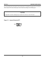
WARNING
TO AVOID MALFUNCTIONS AND COMPONENT DAMAGE, PLEASE READ THE COMPLETE
INSTALLATION PROCEDURE BEFORE THE BOARD IS INSTALLED IN A VMEBUS ENVIRONMENT.
CAUTION
To ensure proper functioning of the product over its usual lifetime, take the following precautions before
handling the board.
Malfunction or damage to the board or connected components:
Electrostatic discharge and incorrect board installation and uninstallation can damage circuits or shorten
their lifetime.
!
!
Before installing or uninstalling the board, read this Installation section
Before installing or uninstalling the board, in a VME rack:
- Check all installed boards for steps that you have to take before turning off the power.
- Take those steps.
- Finally turn off the power.
- Before touching integrated circuits, ensure that you are working in an electrostatic free
environment.
!
Ensure that the board is connected to the VMEbus via all 2 connectors, the P1 and the P2, and that
power is available on all ot them.
!
When operating the board in areas of strong electromagnetic radiation, ensure that the board
- is bolted on the VME rack
- and shielded by closed housing.
This page was intentionally left blank
TABLE OF CONTENTS
1.
GENERAL OVERVIEW . . . . . . . . . . . . . . . . . . . . . . . . . . . . . . . . . . . . . . . . . . . . . . . . . . .
1-1
1.1
The Rotary Switches . . . . . . . . . . . . . . . . . . . . . . . . . . . . . . . . . . . . . . . . . . . . . . . . . . . . .
1-1
1.2
The Function Switch Positions . . . . . . . . . . . . . . . . . . . . . . . . . . . . . . . . . . . . . . . . . . . . . .
1-1
1.3
Connection of the Terminal . . . . . . . . . . . . . . . . . . . . . . . . . . . . . . . . . . . . . . . . . . . . . . . . .
1-3
1.4
The Default Hardware Setup . . . . . . . . . . . . . . . . . . . . . . . . . . . . . . . . . . . . . . . . . . . . . . .
1-4
2.
INSTALLATION IN THE RACK . . . . . . . . . . . . . . . . . . . . . . . . . . . . . . . . . . . . . . . . . . . . .
2-1
2.1
Power ON . . . . . . . . . . . . . . . . . . . . . . . . . . . . . . . . . . . . . . . . . . . . . . . . . . . . . . . . . . . . .
2-1
2.2
Correct Operation . . . . . . . . . . . . . . . . . . . . . . . . . . . . . . . . . . . . . . . . . . . . . . . . . . . . . . . .
2-2
3.
ENVIRONMENTAL REQUIREMENTS . . . . . . . . . . . . . . . . . . . . . . . . . . . . . . . . . . . . . . . .
3-1
LIST OF FIGURES
Figure 1-1:
Front Panel of CPU Board and the Rotary Switch Positions . . . . . . . . . . . . . . . . . . .
1-2
Figure 1-2:
Pinout of the Micro D-Sub and D-Sub Connector for RS232 . . . . . . . . . . . . . . . . . .
1-4
i
This page was intentionally left blank
ii
SECTION 2
INSTALLATION
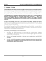
1. GENERAL OVERVIEW
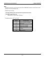
Easy installation of the CPU board is provided since the memory map, the I/O devices, and the interfaces
are configured to communicate with a standard terminal containing RS232 interface.
The monitor (VMEPROM) boots up automatically with the setup of the rotary switches on the front panel.
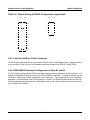
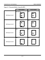
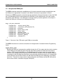
1.1 The Rotary Switches
Two rotary switches are installed on the CPU board to configure the startup of the VMEPROM or a user
program.
The following lists the default configuration for bootup.
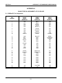
Switch
Hex Code
2
1
$F
$F
The different functions of the rotary switches are described in detail in the Introduction to VMEPROM as
well as in the Hardware User's Manual of this particular CPU board.
1.2 The Function Switch Positions
The CPU board contains two function switches. These two switches are defined as RESET and ABORT.
The RESET switch is located in the first and upper position, and the ABORT switch is located directly
underneath in the second and lower position.
The two moveable positions of these switches are defined as "Up" and "Down".
All function switches must be set to the position "Down" upon performing initial installation.
Please toggle each of the switches before installing the board in the rack in order to detect mechanical
damage to the switches during transport.
1-1
SYS68K/CPU-40/41 USER'S MANUAL
FORCE COMPUTERS
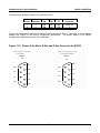
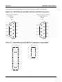
Figure 1-1: Front Panel of CPU Board and the Rotary Switch Positions
1-2
SECTION 2
INSTALLATION
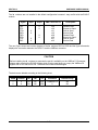
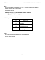
1.3 Connection of the Terminal
The terminal must be connected to the 9-pin Micro D-Sub connector 1 on the CPU board.
The board is delivered with a 9-pin Micro D-Sub to 9-pin D-Sub adapter cable.
The following communication setup is used for interfacing the terminal. Please configure the terminal to
this setup.
No Parity
8 Bits per character
1 Stop Bit
9600 Baud
Asynchronous Protocol
The hardware interface is RS232 compatible. The following signals are supported on the 9-pin Micro D-sub
connector on the front panel:
Signal
Input
DCD
RXD
TXD
DTR
GND
DSR
RTS
CTS
GND
X
X
Output
X
X
X
X
X
X
Required
X
X
X
X
X
9 Pin Micro
D-Sub
Connector
1
2
3
4
5
6
7
8
9
Description
Data Carrier Detect
Receive Data
Transmit Data
Data Terminal Ready
Signal GND
Data Set Ready
Request to Send
Clear to Send
Signal GND
9 Pin D-Sub of the
Adapter Cable
1
2
3
4
5
6
7
8
9
CAUTION
1)
The terminal used must not drive a signal line which is marked to be an output of CPU
board.
2)
All signals marked as "Required" must be supported from the terminal to enable the
transmission.
3)
If the terminal is configured to the listed setup, please connect the 9-pin Micro D-Sub
connector to the terminal with a cable which supports all of the required signals.
1-3
SYS68K/CPU-40/41 USER'S MANUAL
FORCE COMPUTERS
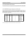
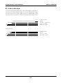
Figure 1-2: Pinout of the Micro D-Sub and D-Sub Connector for RS232
A) Micro DSUB Male Connector Soldered
B) Micro DSUB and DSUB Female Connectors
on the Adapter/Terminal Cable
on the CPU Board
RS232
RS232
Pa
Pa
1
DSR
GND
6
2
RTS
CTS
RTS
4
GND
DSR
5
GND
1-4
4
DTR
3
TXD
2
RXD
1
DCD
7
DTR
9
GND
8
TXD
8
5
9
RXD
7
3
CTS
DCD
6
SECTION 2
INSTALLATION
1.4 The Default Hardware Setup
The VMEbus interface is configured to be used immediately, without any changes.
This results in a default hardware setup which may conflict with other boards installed in the rack.
The following signals are driven/received from the CPU board:
Signal
SYSCLK
BR3*
BR[3..0]*
BG[3..0]OUT*
ACFAIL*
SYSFAIL*
SYSRESET*
Driven
Received
X
X
X
X
X
X
X
X
From
FGA-002 Gate Array
FGA-002 Gate Array
4 Level Arbiter
4 Level Arbiter
FGA-002 Gate Array
FGA-002 Gate Array
FGA-002 Gate Array
CAUTION
1)
The on-board four level arbiter is enabled and reacts on every Bus Request*.
2)
The CPU board is configured as a slot 1 controller.
1-5
SYS68K/CPU-40/41 USER'S MANUAL
FORCE COMPUTERS
This page intentionally left blank
1-6
SECTION 2
INSTALLATION
2. INSTALLATION IN THE RACK
The CPU board can immediately be mounted into a VME rack at slot 1.
CAUTION
1)
Switch off power before installing the board to avoid electrical damage to the
components.
2)
The CPU board contains a special ejector (the handles).
The board must be plugged in, and the screws on the front panel tightened up to
guarantee proper installation.
3)
Unplug every other VMEbus board to avoid conflicts.
2.1 Power ON
Power to the VMEbus rack may be switched on when the board is correctly installed, the switches are in
the correct positions, and the terminal is correctly configured and under power.
Initially, the green RUN LED will light up, and after one to three seconds the message "Wait until hard disk
is up to speed" will be displayed. A few seconds later the VMEPROM banner should appear.
The terminal is now at the user's discretion. At this point, it is advised to make a few carriage returns, to
obtain the question mark (?_) prompt.
2-1
SYS68K/CPU-40/41 USER'S MANUAL
FORCE COMPUTERS
2.2 Correct Operation
To test the correct operation of the CPU board, the following command must be typed in:
? SELFTEST<cr>
It is a matter of a few seconds until all tests are completed. Once all tests are completed, the following
messages will appear on the screen:
VMEPROM Hardware Selftest
I/O test . . . . . .passed
Memory test . . . . .passed
Clock test . . . . . .passed
Any errors will be reported as they occur.
If an error message is displayed, please refer to Section 7, "Introduction to VMEPROM" containing the
command description "SELFTEST".
2-2
SECTION 2
INSTALLATION
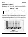
3. ENVIRONMENTAL REQUIREMENTS
This board was specified and tested for reliable operation under certain environmental conditions. Based
on our performance tests, this board is capable of operating within the temperature range of 0oC to 50oC
when used inside of a FORCE TARGET-32 chassis. The following chart details the calculated rate of
forced air cooling.
Rate of Forced Air Cooling
Air Cooling per Board
Total Air Cooling - Target-32
5.5 CFM* = 0.0026 cubic meter/sec
131 CFM = 0.062 cubic meter/sec
275 LFM** = 1.4 meter/sec
275 LFM = 1.4 meter/sec
* CFM = Cubic Feet per Minute
** LFM = Linear Feet per Minute
The TARGET-32 chassis performs forced air cooling using four axial fans. The amount of airflow needed
for cooling and normal operation is reflected by certain factors such as ambient temperature, number and
location of boards in the system, and outside heat sources. Sufficient air cooling is normally obtained when
5.5 CFM and 275 LFM is circulating around each board at an ambient temperature between 0 oC and 50oC.
Allowable storage temperatures may range between -40oC and 85o C. The rate of relative humidity (noncondensing) should not be less than 5%, and should not exceed 95%. The following illustration is a pictorial
view of the fan placement in the chassis.
3-1
HARDWARE USER'S MANUAL
This page was intentionally left blank
TABLE OF CONTENTS
1.
GENERAL INFORMATION . . . . . . . . . . . . . . . . . . . . . . . . . . . . . . . . . . . . . . . . . . . . 1-1
2.
THE PROCESSOR . . . . . . . . . . . . . . . . . . . . . . . . . . . . . . . . . . . . . . . . . . . . . . . . .
2-1
2.1
2.1.1
2.1.1.1
The CPU 68040 . . . . . . . . . . . . . . . . . . . . . . . . . . . . . . . . . . . . . . . . . . . . . . . . . . .
Hardware Interface of the 68040 . . . . . . . . . . . . . . . . . . . . . . . . . . . . . . . . . . . . . . .
General Operation . . . . . . . . . . . . . . . . . . . . . . . . . . . . . . . . . . . . . . . . . . . . . . . . . .
2-1
2-1
2-1
2.2
The Instruction Set . . . . . . . . . . . . . . . . . . . . . . . . . . . . . . . . . . . . . . . . . . . . . . . . .
2-1
2.3
Vector Table of the 68040 . . . . . . . . . . . . . . . . . . . . . . . . . . . . . . . . . . . . . . . . . . . .
2-2
3.
THE LOCAL BUS . . . . . . . . . . . . . . . . . . . . . . . . . . . . . . . . . . . . . . . . . . . . . . . . . .
3-1
3.1
The FGA-002 Gate Array . . . . . . . . . . . . . . . . . . . . . . . . . . . . . . . . . . . . . . . . . . . . .
3-1
3.2
3.2.1
3.2.2
3.2.3
3.2.4
3.2.5
3.2.6
3.2.7
3.2.8
3.2.9
3.2.10
3.2.11
3.2.12
3.2.13
3.2.14
The Shared RAM . . . . . . . . . . . . . . . . . . . . . . . . . . . . . . . . . . . . . . . . . . . . . . . . . . 3-2
General Operation . . . . . . . . . . . . . . . . . . . . . . . . . . . . . . . . . . . . . . . . . . . . . . . . . . 3-2
Shared RAM Information . . . . . . . . . . . . . . . . . . . . . . . . . . . . . . . . . . . . . . . . . . . . . 3-2
The DRM-03 . . . . . . . . . . . . . . . . . . . . . . . . . . . . . . . . . . . . . . . . . . . . . . . . . . . . . . 3-4
RAM Type Information for the DRM-03 . . . . . . . . . . . . . . . . . . . . . . . . . . . . . . . . . . 3-5
Summary of the DRM-03 . . . . . . . . . . . . . . . . . . . . . . . . . . . . . . . . . . . . . . . . . . . . . 3-5
The DRM-05 . . . . . . . . . . . . . . . . . . . . . . . . . . . . . . . . . . . . . . . . . . . . . . . . . . . . . . 3-6
RAM Type Information for the DRM-05 . . . . . . . . . . . . . . . . . . . . . . . . . . . . . . . . . . 3-7
Summary of the DRM-05 . . . . . . . . . . . . . . . . . . . . . . . . . . . . . . . . . . . . . . . . . . . . . 3-7
The SRM-01/4 . . . . . . . . . . . . . . . . . . . . . . . . . . . . . . . . . . . . . . . . . . . . . . . . . . . . . 3-8
RAM Type Information for the SRM-01/4 . . . . . . . . . . . . . . . . . . . . . . . . . . . . . . . . . 3-9
Summary of the SRM-01/4 . . . . . . . . . . . . . . . . . . . . . . . . . . . . . . . . . . . . . . . . . . . 3-9
The SRM-01/8 . . . . . . . . . . . . . . . . . . . . . . . . . . . . . . . . . . . . . . . . . . . . . . . . . . . . . 3-10
RAM Type Information for the SRM-01/8 . . . . . . . . . . . . . . . . . . . . . . . . . . . . . . . . . 3-11
Summary of the SRM-01/8 . . . . . . . . . . . . . . . . . . . . . . . . . . . . . . . . . . . . . . . . . . . 3-11
3.3
3.3.1
3.3.2
3.3.3
3.3.4
3.3.5
The System EPROM Area . . . . . . . . . . . . . . . . . . . . . . . . . . . . . . . . . . . . . . . . . . .
Memory Organization of the System EPROM Area . . . . . . . . . . . . . . . . . . . . . . . .
Usable Device Types for the EPROM Area . . . . . . . . . . . . . . . . . . . . . . . . . . . . . .
Access Time Selection of the System EPROM Area . . . . . . . . . . . . . . . . . . . . . . .
Address Map of the System EPROM Area . . . . . . . . . . . . . . . . . . . . . . . . . . . . . . .
Summary of the EPROM Area . . . . . . . . . . . . . . . . . . . . . . . . . . . . . . . . . . . . . . . .
3-12
3-12
3-15
3-18
3-18
3-18
3.4
3.4.1
The FLXibus . . . . . . . . . . . . . . . . . . . . . . . . . . . . . . . . . . . . . . . . . . . . . . . . . . . . .
Introduction to the FLXibus . . . . . . . . . . . . . . . . . . . . . . . . . . . . . . . . . . . . . . . . . .
3-19
3-19
3.5
3.5.1
3.5.2
3.5.3
3.5.4
3.5.5
3.5.6
The Local FLASH EPROM . . . . . . . . . . . . . . . . . . . . . . . . . . . . . . . . . . . . . . . . . .
Memory Organization of the FLASH EPROM . . . . . . . . . . . . . . . . . . . . . . . . . . . . .
Programming the FLASH EPROM . . . . . . . . . . . . . . . . . . . . . . . . . . . . . . . . . . . . .
Address Map of the FLASH EPROM . . . . . . . . . . . . . . . . . . . . . . . . . . . . . . . . . . .
Summary of the Local FLASH Memory . . . . . . . . . . . . . . . . . . . . . . . . . . . . . . . . .
Jumper Settings for B16 . . . . . . . . . . . . . . . . . . . . . . . . . . . . . . . . . . . . . . . . . . . .
Location Diagram of Jumperfield B16 . . . . . . . . . . . . . . . . . . . . . . . . . . . . . . . . . .
3-20
3-20
3-21
3-21
3-21
3-21
3-22
3.6
The Local SRAM . . . . . . . . . . . . . . . . . . . . . . . . . . . . . . . . . . . . . . . . . . . . . . . . . .
3-23
i
3.6.1
3.6.2
3.6.3
Memory Organization of the User SRAM . . . . . . . . . . . . . . . . . . . . . . . . . . . . . . . .
The Address Map of the SRAM Area . . . . . . . . . . . . . . . . . . . . . . . . . . . . . . . . . . .
Summary of the SRAM Area . . . . . . . . . . . . . . . . . . . . . . . . . . . . . . . . . . . . . . . . .
3-23
3-26
3-26
3.7
3.7.1
The Boot EPROM . . . . . . . . . . . . . . . . . . . . . . . . . . . . . . . . . . . . . . . . . . . . . . . . .
Summary of the Boot EPROM Area . . . . . . . . . . . . . . . . . . . . . . . . . . . . . . . . . . . .
3-27
3-27
3.8
3.8.1
3.8.2
3.8.3
3.8.4
3.8.5
3.8.6
3.8.7
3.8.8
3.8.9
3.8.10
3.8.11
3.8.12
The DUSCC 68562 . . . . . . . . . . . . . . . . . . . . . . . . . . . . . . . . . . . . . . . . . . . . . . . .
Address Map of the DUSCC1 Registers . . . . . . . . . . . . . . . . . . . . . . . . . . . . . . . .
RS232 Hardware Configuration of Port #1 and #2 . . . . . . . . . . . . . . . . . . . . . . . . .
Cable for the Micro D-Sub Connector . . . . . . . . . . . . . . . . . . . . . . . . . . . . . . . . . .
RS422/RS485 Hardware Configuration of Ports #1 and #2 . . . . . . . . . . . . . . . . . .
RS232 and RS422/RS485 Driver Modules FH002 and FH003 . . . . . . . . . . . . . . . .
Summary of DUSCC1 . . . . . . . . . . . . . . . . . . . . . . . . . . . . . . . . . . . . . . . . . . . . . .
Address Map of the DUSCC2 Registers . . . . . . . . . . . . . . . . . . . . . . . . . . . . . . . .
RS232 Hardware Configuration of Ports #3 and #4 . . . . . . . . . . . . . . . . . . . . . . . .
Cable for the Micro D-Sub Connector . . . . . . . . . . . . . . . . . . . . . . . . . . . . . . . . . .
RS422/RS485 Hardware Configuration of Port #3 and #4 . . . . . . . . . . . . . . . . . . .
RS232 and RS422/RS485 Driver Modules FH002 and FH003 . . . . . . . . . . . . . . . .
Summary of DUSCC2 . . . . . . . . . . . . . . . . . . . . . . . . . . . . . . . . . . . . . . . . . . . . . .
3-29
3-30
3-32
3-38
3-38
3-45
3-45
3-46
3-48
3-52
3-52
3-58
3-58
3.9
3.9.1
3.9.2
3.9.3
3.9.4
3.9.5
3.9.6
3.9.7
3.9.8
3.9.9
3.9.10
3.9.11
3.9.12
3.9.13
3.9.14
3.9.15
3.9.16
3.9.17
3.9.18
3.9.19
3.9.20
3.9.21
The PI/T 68230 . . . . . . . . . . . . . . . . . . . . . . . . . . . . . . . . . . . . . . . . . . . . . . . . . . .
Address Map of the PI/T1 Registers . . . . . . . . . . . . . . . . . . . . . . . . . . . . . . . . . . .
I/O Configuration of PI/T1 . . . . . . . . . . . . . . . . . . . . . . . . . . . . . . . . . . . . . . . . . . .
Rotary Switches . . . . . . . . . . . . . . . . . . . . . . . . . . . . . . . . . . . . . . . . . . . . . . . . . .
Lock Cycles . . . . . . . . . . . . . . . . . . . . . . . . . . . . . . . . . . . . . . . . . . . . . . . . . . . . . .
Interrupt Request Signal . . . . . . . . . . . . . . . . . . . . . . . . . . . . . . . . . . . . . . . . . . . .
A24 Slave Mode . . . . . . . . . . . . . . . . . . . . . . . . . . . . . . . . . . . . . . . . . . . . . . . . . .
Reserved Lines . . . . . . . . . . . . . . . . . . . . . . . . . . . . . . . . . . . . . . . . . . . . . . . . . . .
Summary of PI/T1 . . . . . . . . . . . . . . . . . . . . . . . . . . . . . . . . . . . . . . . . . . . . . . . . .
Address Map of the PI/T2 Registers . . . . . . . . . . . . . . . . . . . . . . . . . . . . . . . . . . .
I/O Configuration of PI/T2 . . . . . . . . . . . . . . . . . . . . . . . . . . . . . . . . . . . . . . . . . . .
Memory Size Recognition . . . . . . . . . . . . . . . . . . . . . . . . . . . . . . . . . . . . . . . . . . .
Board Identification . . . . . . . . . . . . . . . . . . . . . . . . . . . . . . . . . . . . . . . . . . . . . . . .
Interrupt Request Signal . . . . . . . . . . . . . . . . . . . . . . . . . . . . . . . . . . . . . . . . . . . .
12 Bit I/O Port . . . . . . . . . . . . . . . . . . . . . . . . . . . . . . . . . . . . . . . . . . . . . . . . . . . .
MODLOW . . . . . . . . . . . . . . . . . . . . . . . . . . . . . . . . . . . . . . . . . . . . . . . . . . . . . . .
RAM Module Configuration Signals . . . . . . . . . . . . . . . . . . . . . . . . . . . . . . . . . . . .
Timer IRQ/Reset . . . . . . . . . . . . . . . . . . . . . . . . . . . . . . . . . . . . . . . . . . . . . . . . . .
PIRQ . . . . . . . . . . . . . . . . . . . . . . . . . . . . . . . . . . . . . . . . . . . . . . . . . . . . . . . . . . .
Enable A24 Slave Mode . . . . . . . . . . . . . . . . . . . . . . . . . . . . . . . . . . . . . . . . . . . .
Reserved Line . . . . . . . . . . . . . . . . . . . . . . . . . . . . . . . . . . . . . . . . . . . . . . . . . . . .
Summary of PI/T2 . . . . . . . . . . . . . . . . . . . . . . . . . . . . . . . . . . . . . . . . . . . . . . . . .
3-59
3-60
3-61
3-62
3-64
3-65
3-65
3-65
3-66
3-67
3-68
3-69
3-69
3-69
3-70
3-72
3-72
3-73
3-73
3-73
3-74
3-74
3.10
3.10.1
3.10.2
3.10.3
The Real Time Clock (RTC) 72423 . . . . . . . . . . . . . . . . . . . . . . . . . . . . . . . . . . . .
Address Map of the RTC Registers . . . . . . . . . . . . . . . . . . . . . . . . . . . . . . . . . . . .
RTC Programming . . . . . . . . . . . . . . . . . . . . . . . . . . . . . . . . . . . . . . . . . . . . . . . .
Summary of the RTC . . . . . . . . . . . . . . . . . . . . . . . . . . . . . . . . . . . . . . . . . . . . . . .
3-75
3-75
3-75
3-79
4.
FUNCTION SWITCHES AND INDICATION LEDs . . . . . . . . . . . . . . . . . . . . . . . . . .
4-1
4.1
RESET Function Switch . . . . . . . . . . . . . . . . . . . . . . . . . . . . . . . . . . . . . . . . . . . . .
4-1
ii
4.2
ABORT Function Switch . . . . . . . . . . . . . . . . . . . . . . . . . . . . . . . . . . . . . . . . . . . . .
4-1
4.3
"RUN" LED . . . . . . . . . . . . . . . . . . . . . . . . . . . . . . . . . . . . . . . . . . . . . . . . . . . . . . .
4-2
4.4
"BM" LED . . . . . . . . . . . . . . . . . . . . . . . . . . . . . . . . . . . . . . . . . . . . . . . . . . . . . . . .
4-2
4.5
Rotary Switches . . . . . . . . . . . . . . . . . . . . . . . . . . . . . . . . . . . . . . . . . . . . . . . . . . .
4-2
5.
THE CPU BOARD INTERRUPT STRUCTURE . . . . . . . . . . . . . . . . . . . . . . . . . . . .
5-1
6.
VMEBUS INTERFACE . . . . . . . . . . . . . . . . . . . . . . . . . . . . . . . . . . . . . . . . . . . . . .
6-1
6.1
6.1.1
6.1.2
VMEbus Master Interface . . . . . . . . . . . . . . . . . . . . . . . . . . . . . . . . . . . . . . . . . . . .
Data Transfer Size of the VMEbus Interface . . . . . . . . . . . . . . . . . . . . . . . . . . . . . .
Address Modifier Implementation . . . . . . . . . . . . . . . . . . . . . . . . . . . . . . . . . . . . . .
6-1
6-1
6-4
6.2
6.2.1
6.2.2
6.2.3
VMEbus Slave Interface . . . . . . . . . . . . . . . . . . . . . . . . . . . . . . . . . . . . . . . . . . . . .
The Access Address . . . . . . . . . . . . . . . . . . . . . . . . . . . . . . . . . . . . . . . . . . . . . . . .
Data Transfer Size of the Shared RAM . . . . . . . . . . . . . . . . . . . . . . . . . . . . . . . . . .
Address Modifier Decoding and A24 Slave Mode . . . . . . . . . . . . . . . . . . . . . . . . . .
6-8
6-8
6-8
6-8
6.3
The VMEbus Interrupt Handler . . . . . . . . . . . . . . . . . . . . . . . . . . . . . . . . . . . . . . .
6-11
6.4
6.4.1
6.4.2
6.4.3
6.4.3.1
6.4.3.2
6.4.3.3
6.4.3.4
6.4.3.5
6.4.3.6
6.4.3.7
VMEbus Arbitration . . . . . . . . . . . . . . . . . . . . . . . . . . . . . . . . . . . . . . . . . . . . . . . .
Four Available VMEbus Arbiters . . . . . . . . . . . . . . . . . . . . . . . . . . . . . . . . . . . . . .
The On-Board Four Level Arbiter . . . . . . . . . . . . . . . . . . . . . . . . . . . . . . . . . . . . . .
The VMEbus Release Function . . . . . . . . . . . . . . . . . . . . . . . . . . . . . . . . . . . . . . .
Release Every Cycle (REC) . . . . . . . . . . . . . . . . . . . . . . . . . . . . . . . . . . . . . . . . . .
Release on Request (ROR) . . . . . . . . . . . . . . . . . . . . . . . . . . . . . . . . . . . . . . . . . .
Release After Timeout (RAT) . . . . . . . . . . . . . . . . . . . . . . . . . . . . . . . . . . . . . . . .
Release on Bus Clear (RBCLR) . . . . . . . . . . . . . . . . . . . . . . . . . . . . . . . . . . . . . . .
Release When Done (RWD) . . . . . . . . . . . . . . . . . . . . . . . . . . . . . . . . . . . . . . . . .
Release Voluntary (RV) . . . . . . . . . . . . . . . . . . . . . . . . . . . . . . . . . . . . . . . . . . . . .
Release on ACFAIL (ACFAIL) . . . . . . . . . . . . . . . . . . . . . . . . . . . . . . . . . . . . . . . .
6-12
6-12
6-12
6-18
6-18
6-18
6-18
6-19
6-19
6-19
6-19
6.5
6.5.1
6.5.2
The VMEbus Interrupter . . . . . . . . . . . . . . . . . . . . . . . . . . . . . . . . . . . . . . . . . . . .
The Interrupt Generation Register . . . . . . . . . . . . . . . . . . . . . . . . . . . . . . . . . . . . .
The Interrupt Vector Register . . . . . . . . . . . . . . . . . . . . . . . . . . . . . . . . . . . . . . . .
6-21
6-21
6-22
6.6
The SYSCLK Driver . . . . . . . . . . . . . . . . . . . . . . . . . . . . . . . . . . . . . . . . . . . . . . .
6-23
6.7
Exception Signals . . . . . . . . . . . . . . . . . . . . . . . . . . . . . . . . . . . . . . . . . . . . . . . . .
6-25
6.8
6.8.1
6.8.2
6.8.3
6.8.3.1
RESET Generation . . . . . . . . . . . . . . . . . . . . . . . . . . . . . . . . . . . . . . . . . . . . . . . .
The Front Panel RESET Switch . . . . . . . . . . . . . . . . . . . . . . . . . . . . . . . . . . . . . .
The Voltage Sensor Module FH001 . . . . . . . . . . . . . . . . . . . . . . . . . . . . . . . . . . . .
VMEbus RESET Conditions . . . . . . . . . . . . . . . . . . . . . . . . . . . . . . . . . . . . . . . . .
Receive RESET from VMEbus . . . . . . . . . . . . . . . . . . . . . . . . . . . . . . . . . . . . . . .
6-27
6-27
6-27
6-29
6-29
6.8.3.2
6.8.3.3
6.8.4
Drive RESET to VMEbus . . . . . . . . . . . . . . . . . . . . . . . . . . . . . . . . . . . . . . . . . . . .
Default Configuration of Jumperfield B13 . . . . . . . . . . . . . . . . . . . . . . . . . . . . . . . .
The RESET Instruction . . . . . . . . . . . . . . . . . . . . . . . . . . . . . . . . . . . . . . . . . . . . .
6-29
6-29
6-31
iii
LIST OF FIGURES
Figure 2-1:
Figure 2-2:
Figure 3-1:
Figure 3-2:
Figure 3-3:
Figure 3-4:
Figure 3-5:
Figure 3-6:
Figure 3-7:
Figure 3-8:
Figure 3-9:
Figure 3-10:
Figure 3-11:
Figure 3-12:
Figure 3-13:
Figure 3-14:
Figure 3-15:
...
Figure 3-16:
Figure 3-17:
Figure 3-18:
Figure 3-19:
Figure 3-20:
Figure 3-21:
Figure 3-22:
Figure 3-23:
Figure 3-24:
Figure 3-25:
Figure 3-26:
Figure 3-27:
Figure 4-1:
Figure 6-1:
Figure 6-2:
Figure 6-3:
Figure 6-4:
Figure 6-5:
Figure 6-6:
Figure 6-7:
Figure 6-8:
Figure 6-9:
.
Jumper Setting for B17 . . . . . . . . . . . . . . . . . . . . . . . . . . . . . . . . . . . . . . . . . . . . . .
Location Diagram of Jumperfields B17 . . . . . . . . . . . . . . . . . . . . . . . . . . . . . . . . . .
Memory Organization of the System EPROM Area . . . . . . . . . . . . . . . . . . . . . . . .
Location Diagram of the System EPROM Area . . . . . . . . . . . . . . . . . . . . . . . . . . .
Configuration Jumper Settings of System EPROM Area Jumperfield B11 . . . . . . .
Location Diagram of Jumperfield B11 Configuration of the System EPROM Area .
Location Diagram of the Backup Supply Jumperfield B1 and B20 . . . . . . . . . . . . .
Location Diagram of the Boot EPROM . . . . . . . . . . . . . . . . . . . . . . . . . . . . . . . . .
Location Diagram of the 0S Resistors R563 to R569 . . . . . . . . . . . . . . . . . . . . . . .
RS232 Connection Between DUSCC1 and VMEbus Connector P2 . . . . . . . . . . . .
RS232 Connection Between DUSCC1 and Micro D-Sub Connector . . . . . . . . . . . .
Pinout of the Micro D-Sub and D-Sub Connector for RS232 . . . . . . . . . . . . . . . . .
Location Diagram of RS232 Configuration Jumperfields B3, B4, B5, and B6 . . . . .
Location Diagram of the 0S Resistors R563 to R569 . . . . . . . . . . . . . . . . . . . . . . .
RS422/RS485 Connection between DUSCC1 and VMEbus Connector P2 . . . . . .
RS422/RS485 Pinout of the Micro D-Sub and D-Sub Connectors . . . . . . . . . . . . .
Location Diagram of RS422/RS485 Configuration Jumperfields B3, B4, B5, and B6
................................................................
Location Diagram of RS232/RS422/RS485 Driver/Receivers J20 and J21 plus
Resistor Arrays J22 and J23 . . . . . . . . . . . . . . . . . . . . . . . . . . . . . . . . . . . . . . . . .
Connection Between DUSCC2 and D-Sub Connector for RS232 . . . . . . . . . . . . . .
Location Diagram of RS232 Configuration Jumperfields B7 through B10 . . . . . . . .
RS232 Pinout of the Micro D-Sub and D-Sub Connectors . . . . . . . . . . . . . . . . . . .
Connection between DUSCC2 and Micro D-Sub Connector for RS422/RS485 . . .
Location Diagram of RS422/RS485 Configuration Jumperfields B7 through B10 . .
RS422/RS485 Pinout of the Micro D-Sub and D-Sub Connectors . . . . . . . . . . . . .
Location Diagram of RS232/RS422/RS485 Driver/Receiver J25/J26 and Resistor
Arrays J27/J28 . . . . . . . . . . . . . . . . . . . . . . . . . . . . . . . . . . . . . . . . . . . . . . . . . . .
CPU Board Front Panel and Rotary Switch Positions . . . . . . . . . . . . . . . . . . . . . . .
Location Diagram of Header B12 . . . . . . . . . . . . . . . . . . . . . . . . . . . . . . . . . . . . . .
RTC Programming Example . . . . . . . . . . . . . . . . . . . . . . . . . . . . . . . . . . . . . . . . .
Location Diagram of the Backup Supply Jumperfield B1 and B20 . . . . . . . . . . . . .
Front Panel of the CPU Board . . . . . . . . . . . . . . . . . . . . . . . . . . . . . . . . . . . . . . . . .
Requester/Arbiter Jumperfield B19 . . . . . . . . . . . . . . . . . . . . . . . . . . . . . . . . . . . .
Location Diagram of Jumperfield B19 . . . . . . . . . . . . . . . . . . . . . . . . . . . . . . . . . .
Usage of Jumperfield B13 . . . . . . . . . . . . . . . . . . . . . . . . . . . . . . . . . . . . . . . . . . .
Location Diagram of B13 . . . . . . . . . . . . . . . . . . . . . . . . . . . . . . . . . . . . . . . . . . . .
Usage of Jumperfield B13 . . . . . . . . . . . . . . . . . . . . . . . . . . . . . . . . . . . . . . . . . . .
Location Diagram of Jumperfield B13 . . . . . . . . . . . . . . . . . . . . . . . . . . . . . . . . . .
Jumper Settings for Jumperfield B2 . . . . . . . . . . . . . . . . . . . . . . . . . . . . . . . . . . . .
Location Diagram of Jumperfield B2 . . . . . . . . . . . . . . . . . . . . . . . . . . . . . . . . . . .
Location Diagram of Jumperfield B13 . . . . . . . . . . . . . . . . . . . . . . . . . . . . . . . . . .
iv
2-3
2-4
3-12
3-13
3-16
3-17
3-25
3-28
3-34
3-35
3-35
3-35
3-37
3-40
3-41
3-42
3-43
3-44
3-49
3-50
3-51
3-53
3-54
3-55
3-57
3-63
3-71
3-76
3-78
4-3
6-16
6-17
6-23
6-24
6-25
6-26
6-27
6-28
6-30
LIST OF TABLES
Table 2-1:
Table 3-1:
Table 3-2:
Table 3-3:
Table 3-4:
Table 3-5:
Table 3-6:
Table 3-7:
Table 3-8:
Table 3-9:
Table 3-10:
Table 3-11:
Table 3-12:
Table 3-13:
Table 3-14:
Table 3-15:
Table 3-16:
Table 3-18:
Table 3-17:
Table 6-1:
Table 6-2:
Table 6-3:
Table 6-4:
Table 6-5:
Table 6-6:
Table 6-7:
Table 6-8:
Table 6-9:
Table 6-10:
Table 6-11:
Table 6-12:
Table 6-13:
Table 6-14:
Exception Vector Assignments . . . . . . . . . . . . . . . . . . . . . . . . . . . . . . . . . . . . . . . .
Address Map of the EPROM Area . . . . . . . . . . . . . . . . . . . . . . . . . . . . . . . . . . . . .
Serial I/O Port #1 (DUSCC1) Register Address Map . . . . . . . . . . . . . . . . . . . . . . .
Serial I/O Port #2 (DUSCC1) Register Address Map . . . . . . . . . . . . . . . . . . . . . . .
Ports #1 and #2 (DUSCC1) Common Register Address Map . . . . . . . . . . . . . . . . .
Default Setting of RS232 Configuration Jumperfields . . . . . . . . . . . . . . . . . . . . . . .
RS422/RS485 Configuration Jumperfield Settings . . . . . . . . . . . . . . . . . . . . . . . . .
PCB Locations for the RS232/RS422/RS485 Configuration . . . . . . . . . . . . . . . . . .
Serial I/O Port #3 (DUSCC2) Register Address Map . . . . . . . . . . . . . . . . . . . . . . .
Serial I/O Port #4 (DUSCC2) Register Address Map . . . . . . . . . . . . . . . . . . . . . . .
Ports #3 and #4 (DUSCC2) Common Registers Address Map . . . . . . . . . . . . . . . .
Default Setting of the RS232 Configuration Jumperfields . . . . . . . . . . . . . . . . . . . .
RS422/RS485 Configuration Jumperfield Setting . . . . . . . . . . . . . . . . . . . . . . . . . .
PCB Locations for RS232/RS422/RS485 Configuration . . . . . . . . . . . . . . . . . . . . .
PI/T1 Register Layout . . . . . . . . . . . . . . . . . . . . . . . . . . . . . . . . . . . . . . . . . . . . . .
PI/T1 Interface Signals . . . . . . . . . . . . . . . . . . . . . . . . . . . . . . . . . . . . . . . . . . . . .
PI/T2 Register Layout . . . . . . . . . . . . . . . . . . . . . . . . . . . . . . . . . . . . . . . . . . . . . .
PI/T2 Interface Signals . . . . . . . . . . . . . . . . . . . . . . . . . . . . . . . . . . . . . . . . . . . . .
RTC Register Layout . . . . . . . . . . . . . . . . . . . . . . . . . . . . . . . . . . . . . . . . . . . . . . .
Data Bus Size of the VMEbus . . . . . . . . . . . . . . . . . . . . . . . . . . . . . . . . . . . . . . . . .
Defined VMEbus Transfer Cycles (D32 Mode) . . . . . . . . . . . . . . . . . . . . . . . . . . . . .
Defined VMEbus Transfer Cycles (D16 Mode) . . . . . . . . . . . . . . . . . . . . . . . . . . . . .
Address Ranges . . . . . . . . . . . . . . . . . . . . . . . . . . . . . . . . . . . . . . . . . . . . . . . . . . .
Address Modifier Codes . . . . . . . . . . . . . . . . . . . . . . . . . . . . . . . . . . . . . . . . . . . . .
Address Modifier Codes Used on the CPU Board . . . . . . . . . . . . . . . . . . . . . . . . . .
VMEbus Slave AM Codes . . . . . . . . . . . . . . . . . . . . . . . . . . . . . . . . . . . . . . . . . . .
VMEbus Arbiter/Requester Register Layout . . . . . . . . . . . . . . . . . . . . . . . . . . . . . .
Description of Arbiter/Requester Register Bits . . . . . . . . . . . . . . . . . . . . . . . . . . . .
Bit Settings for VMEbus Request Level . . . . . . . . . . . . . . . . . . . . . . . . . . . . . . . . .
Bit Settings for VMEbus Arbiter Mode . . . . . . . . . . . . . . . . . . . . . . . . . . . . . . . . . .
Bus Release Functions . . . . . . . . . . . . . . . . . . . . . . . . . . . . . . . . . . . . . . . . . . . . .
VMEbus Interrupter Registers . . . . . . . . . . . . . . . . . . . . . . . . . . . . . . . . . . . . . . . .
Description of the IRQ Generation Register . . . . . . . . . . . . . . . . . . . . . . . . . . . . . .
v
2-2
3-18
3-30
3-31
3-31
3-38
3-41
3-42
3-46
3-47
3-48
3-51
3-55
3-56
3-60
3-61
3-67
3-68
3-75
6-2
6-3
6-3
6-4
6-5
6-7
6-10
6-13
6-13
6-14
6-15
6-20
6-21
6-22
This page was intentionally left blank
vi
SECTION 3
HARDWARE USER'S MANUAL
1. GENERAL INFORMATION
This CPU board is a high performance single board computer based on the 68040 microprocessor and the
VMEbus. The board incorporates a modular I/O subsystem which provides a high degree of flexibility for
a wide variety of applications. The CPU board can be used with or without an I/O subsystem, called an
"EAGLE" module.
The board is able to hold a RAM Module which can be DRAM (CPU-40) or SRAM (CPU-41) based.
The CPU-40/41 family design utilizes all of the features of the powerful FORCE Gate Array (FGA-002).
Among its features is a 32-bit DMA controller which supports local (shared) memory, VMEbus and I/O data
transfers for maximum performance, parallel real time operation and responsiveness.
The EAGLE modules are installed on the CPU board via the FLXi (FORCE Local eXpansion interface). This
provides a full 32-bit interface between the base board and the EAGLE module I/O subsystem, providing
a range of I/O options.
Four multiprotocol serial I/O channels, a parallel I/O channel and a Real Time Clock with on-board battery
backup are installed on the base board which, in combination with EAGLE modules, makes the CPU board
a true single board computer system.
A broad range of operating systems and kernels is available for the CPU board. However, as with all
FORCE COMPUTERS' CPU cards, VMEPROM firmware is provided with the board at no extra cost.
VMEPROM is a Real Time Kernel and is installed on the CPU board in the 16-bit wide EPROM sockets,
which results in a 32-bit wide System EPROM area. This ensures that the board is supplied ready to use.
1-1
SYS68K/CPU-40/41 USER'S MANUAL
FORCE COMPUTERS
This page intentionally left blank
1-2
SECTION 3
HARDWARE USER'S MANUAL
2. THE PROCESSOR
2.1 The CPU 68040
2.1.1 Hardware Interface of the 68040
The 68040 uses a nonmultiplexed 32-bit address and 32-bit data bus. The 68040 does not support the
dynamic bus sizing like the 68020 or 68030. On this CPU board the dynamic bus sizing is built in external
hardware (two programmable gate arrays). This means if the 68040 does a long word read from a byte
device, the external hardware will fetch 4 bytes from this byte wide device, from a long word and
acknowledge the access cycle to the 68040. Therefore all device drives within the 68020 or 68030 can be
used on this CPU board. Please note that the 68040 has a 4 Kbyte instruction and a 4 Kbyte data cache
which may cause problems.
2.1.1.1 General Operation
The CPU drives the address lines (A0-A31), the size lines (SIZ0, SIZ1) the transfer type (TT0-TT1) on every
cycle, and modifier (TM0-2) signals independent of a cache hit or miss. These signals are used to decode
the memory map of the CPU board.
The transfer start (TS) signals the hardware on the CPU board that the current cycle is not a cache cycle,
and that the decoding outputs are valid.
The 32 data lines (D0-D31) are also driven from the processor on write cycles and sensed on read cycles.
The size of the data transfer is defined by the SIZE output signals (always driven from the CPU when
master). The transfer acknowledge or the transfer error acknowledge signal (TA, TEA) or both terminate
the transfer cycle. CPU 68040 cycles only allow a port width of 32 bits.
If an access error occurs (TEA sensed from the CPU), exception handling starts because the current cycle
has been aborted (illegal transfer or wrong data).
During local bus operation, an access error will be generated if a device does not respond correctly.
VMEbus transfers may also be aborted via a TEA (VMEbus : BERR*).
The TA and TEA signal asserted simultaneously initiate a retry cycle.
2.2 The Instruction Set
For the 68040 instruction set and further information relative to programming, please refer to the 68040
User's Manual.
2-1
SYS68K/CPU-40/41 USER'S MANUAL
FORCE COMPUTERS
2.3 Vector Table of the 68040
The following table lists all vectors defined and used by the 68040 CPU.
Table 2-1: Exception Vector Assignments
Vector
Number(s)
Vector Offset
(Hex)
Assignment
0
1
2
3
000
004
008
00C
Reset Initial Interrupt Stack Pointer
Reset Initial Program Counter
Access Fault (Bus Error)
Address Error
4
5
6
7
010
014
018
01C
Illegal Instruction
Integer Divide by Zero
CHK, CHK2 Instruction
FTRAPcc, TRAPcc, TRAPV Instructions
8
9
10
11
020
024
028
02C
Privilege Violation
Trace
Line 1010 Emulator (Unimplemented A-Line Opcode)
Line 1111 Emulator (Unimplemented F-Line Opcode)
12
13
14
15
030
034
038
03C
(Unassigned, Reserved)
Defined for MC68020/MC68030, not for MC68040
Format Error
Uninitialized Interrupt
16-23
040-05C
24
25
26
27
060
064
068
06C
Spurious Interrupt
Level 1 Interrupt Autovector
Level 2 Interrupt Autovector
Level 3 Interrupt Autovector
28
29
30
31
070
074
078
07C
Level 4 Interrupt Autovector
Level 5 Interrupt Autovector
Level 6 Interrupt Autovector
Level 7 Interrupt Autovector
32-47
080-0BC
48
49
50
51
0C0
0C4
0C8
OCC
FP Branch or Set on Unordered Condition
FP Inexact Result
FP Divide by Zero
FP Underflow
52
53
54
55
ODO
OD4
0D8
ODC
FP Operand Error
FP Overflow
FP Signaling NAN
FP Unimplemented Data Type
56
57
58
0E0
0E4
0E8
Defined for MC68030 and MC68851, not for MC68040
Defined for MC68851, not for MC68040
Defined for MC68851, not for MC68040
59-63
0EC-0FC
(Unassigned, Reserved)
64-255
100-3FC
User Defined Vectors (192)
(Unassigned, Reserved)
TRAP #0-15 Instruction Vectors
2-2
SECTION 3
HARDWARE USER'S MANUAL
For test purposes the clock signal for the microprocessor is connected via jumper B17 to the devices.
When using the CPU board, this jumper must be inserted according to the following figure.
CAUTION
If jumper B17 is removed, damage may be caused to the devices on the CPU board.
Figure 2-1: Jumper Setting for B17
+)))))))),
B17 * o)))) o *
.))))))))2
1
2-3
SYS68K/CPU-40/41 USER'S MANUAL
FORCE COMPUTERS
Figure 2-2: Location Diagram of Jumperfields B17
2-4
SECTION 3
HARDWARE USER'S MANUAL
3. THE LOCAL BUS
3.1 The FGA-002 Gate Array
The FGA-002 Gate Array featured on this CPU board has 24,000 gates and 281 pins.
The FGA-002 Gate Array controls the local bus and builds the interface to the VMEbus. It also includes
a DMA controller, complete interrupt management, a message broadcast interface (FMB), timer functions,
and mailbox locations.
This gate array monitors the local bus. This in turn signifies that if any local device is to be accessed, the
gate array takes charge of all control signals in addition to used address and data signals.
The FGA-002 Gate Array serves as a manager for the VMEbus. All VMEbus address and data lines are
connected to the gate array through the buffers. Additional functions such as the VMEbus interrupt handler
are also installed on the FGA-002 Gate Array. The SGL VMEbus arbiter in the FGA/002 must remain
disabled because the 4 level VME arbiter of the CPU board is designed in a separate device and connected
with the VME bus (please refer to chapter 6.4 VMEbus Arbitration for further information).
The start address of the FGA-002 Gate Array registers is $FFD00000. All registers of the gate array and
associated functions are described in detail in the FGA-002 Gate Array User's Manual.
3-1
SYS68K/CPU-40/41 USER'S MANUAL
FORCE COMPUTERS
3.2 The Shared RAM
On this CPU board the shared RAM is placed on a module to allow the adaptation of DRAM or SRAM to
the base board.
All signals which are needed to control the shared RAM are available on the RAM module connector.
Therefore RAM devices with different access times can also be used on this CPU board to take advantage
of the 68040 with higher frequency if it becomes available.
3.2.1 General Operation
The Shared RAM is accessible from the 68040 and from the VMEbus. The access address for the 68040
starts at $00000000. The access address for the VMEbus is software programmable in 4 Kbyte steps. The
defined memory range can be write protected in coordination with the address modifier codes. For
example, in supervisor mode the memory can be read and written, in user mode memory can only be read.
If an access from the VMEbus takes place the onboard logic requests the local bus mastership from the
local arbiter via the FGA-002 Gate Array. After the arbiter has granted local bus mastership to the FGA-002
Gate Array, the access cycle is executed. A read cycle is terminated by latching all data from the memory;
a write cycle is ended by storing the data in the memory cells. Both read and write cycles are terminated
on the local bus side and the FGA-002 Gate Array immediately releases bus mastership to the CPU while
completing the fully asynchronous VMEbus access cycle.
3.2.2 Shared RAM Information
The RAM module connector holds several signals which are software readable and inform the user
concerning RAM type and functionality.
These pins are readable via the PI/T2 device which is installed on the CPU board. For base address and
register address information please refer to the chapter 3.9.9 Address Map of the PI/T2 Registers for
further information.
3-2
SECTION 3
HARDWARE USER'S MANUAL
The following table shows the information which can be read and the corresponding PI/T bit. The RAM
modules which are accessible are described in the following chapters which also contain the RAM Type
Information description.
RAM Type Information on PI/T2
PI/T Bit
Name
Value
Description
PB0
PB1
PB2
MCD0
MCD1
MCD2
*
*
*
Describes the memory size of the module.
Please refer to the following chapters.
PC2
RAMTYP
0
1
SRAM
DRAM
PC4
BURST
0
1
Not available
Available
PC6
PARITY
0
1
Not available
Available
3-3
SYS68K/CPU-40/41 USER'S MANUAL
FORCE COMPUTERS
3.2.3 The DRM-03
The following CPU board is assembled with the DRM-03.
CPU Board
RAM Module
RAM Capacity
CPU-40B/4/xx
DRM-03/4
4 Mbyte
"xx" contains the EAGLE module number and is independent of the RAM module.
Features of the DRM-03
!
4 Mbyte DRAM
!
Burst READ and Burst WRITE capability
!
Parity Generation and Checking
!
Asynchronous refresh is provided every 14µs
!
Accessible via VMEbus
The access address for the 68040 is as follows:
RAM Module
Access Address
DRM-03/4
$ 0000 0000 .. $ 003F FFFF
The access address for the VMEbus is programmable in 4 Kbyte steps through the FGA-002. The defined
memory range can be write protected in coordination with the address modifier codes. For example, in
supervisor mode the memory can be read and written, in user mode memory can only be read.
The DRAM module includes byte parity check for local and VMEbus accesses. If a parity error is detected
on a VMEbus cycle, a BERR is forced to the VMEbus informing the requestor that a parity error has
occurred. On local accesses, a Transfer Error Acknowledge (TEA) is forced to the processor if a parity
error was detected. The chart on the next page lists the required CPU clock cycles and wait states for
accessing the shared RAM.
The following chart lists the required CPU clock cycles and wait states for accessing the shared RAM.
3-4
SECTION 3
HARDWARE USER'S MANUAL
Board
Type
68040 Clock
Frequency
No. of CPU Clock
Cycles Counted
From TS to TA
for Normal Cycles
No. of CPU Clock
Cycles for
Burst Cycles
No. of Wait
States for
Normal Cycles
No. of Wait
States for
Burst Cycles
CPU-40/B
25 MHz
4
1
3
0
3.2.4 RAM Type Information for the DRM-03
The following information can be read from the PI/T2.
RAM Type Information
PI/T Bit
Name
DRM-03/4
PB0
PB1
PB2
MCD4
MCD1
MCD2
1
1
0
PC2
RAMTYP
1
PC4
BURST
1
PC6
PARITY
1
3.2.5 Summary of the DRM-03
Capacity
4 Mbyte
Port Data Width
32 bits
Local Data Width
128 bits and 16 bit parity
Burst Mode
Supported
Parity Mode
Supported
Device
256K x 18 Fast Page Mode
Supported Transfers
Byte, Word, Long word, Cache Line (16 bytes)
3-5
SYS68K/CPU-40/41 USER'S MANUAL
FORCE COMPUTERS
3.2.6 The DRM-05
The following CPU boards are assembled with the DRM-05.
CPU Board
RAM Module
RAM Capacity
CPU-40B/16/xx
CPU-40B/32/xx
DRM-05/16
DRM-05/32
16 Mbyte
32 Mbyte
"xx" contains the EAGLE module number and is independent of the RAM module.
Features of the DRM-05
!
16 or 32 Mbyte DRAM
!
Burst READ and Burst WRITE capability
!
Parity Generation and Checking
!
Asynchronous refresh is provided every 14µs
!
Accessible via VMEbus
The access address for the 68040 is as follows:
RAM Module
Access Address
DRM-05/16
DRM-05/32
$ 0000 0000 .. $ 00FF FFFF
$ 0000 0000 .. $ 01FF FFFF
The access address for the VMEbus is programmable in 4 Kbyte steps through the FGA-002. The defined
memory range can be write protected in coordination with the address modifier codes. For example, in
supervisor mode the memory can be read and written, in user mode memory can only be read.
The DRAM module includes byte parity check for local and VMEbus accesses. If a parity error is detected
on a VMEbus cycle, a BERR is forced to the VMEbus informing the requestor that a parity error has
occurred. On local accesses, a Transfer Error Acknowledge (TEA) is forced to the processor if a parity
error was detected. The chart on the next page lists the required CPU clock cycles and wait states for
accessing the shared RAM.
The following chart lists the required CPU clock cycles and wait states for accessing the shared RAM.
3-6
SECTION 3
HARDWARE USER'S MANUAL
Board
Type
68040 Clock
Frequency
No. of CPU Clock
Cycles Counted
From TS to TA
for Normal
Cycles
No. of CPU Clock
Cycles for
Burst Cycles
No. of Wait
States for
Normal Cycles
No. of Wait
States for
Burst Cycles
CPU-40/B
25 MHz
4
1
3
0
3.2.7 RAM Type Information for the DRM-05
The following information can be read from the PI/T2.
RAM Type Information
PI/T Bit
Name
DRAM-05/16
DRAM-05/32
PB0
PB1
PB2
MCD4
MCD1
MCD2
1
0
0
0
0
0
PC2
RAMTYP
1
1
PC4
BURST
1
1
PC6
PARITY
1
1
3.2.8 Summary of the DRM-05
Capacity
16 or 32 Mbyte
Port Data Width
32 bits
Local Data Width
128 bits and 16 bit parity
Burst Mode
Supported
Parity Mode
Supported
Device
1M x 4 /4M x 1 Fast Page Mode
Supported Transfers
Byte, Word, Long word, Cache Line (16 bytes)
3-7
SYS68K/CPU-40/41 USER'S MANUAL
FORCE COMPUTERS
3.2.9 The SRM-01/4
The following CPU boards are assembled with the SRM-01/4.
CPU Board
RAM Module
CPU-41B/4/xx
SRM-01/4
"xx" contains the EAGLE module number and is independent for the RAM module.
The SRM-01/4 is a 4 Mbyte RAM module using Static Memory devices. The RAM module has the following
features.
Features of the SRM-01/4
!
4 Mbyte SRAM
!
Burst READ and Burst WRITE capability
!
Battery Backup via VMEbus
!
Accessible via VMEbus
The access address for the 68040 is $00000000 to $003FFFFF.
The access address for the VMEbus is programmable in 4 Kbyte steps through the FGA-002. The defined
memory range can be write protected in coordination with the address modifier codes. For example, in
supervisor mode the memory can be read and written, in user mode memory can only be read.
Parity check is not necessary for SRAM devices because these components are protected against soft
errors owing to alpha emission. The following chart lists the required CPU clock cycles and wait states for
accessing the shared RAM.
Board
Type
68040 Clock
Frequency
No. of CPU Clock
Cycles Counted
From TS to TA
for Normal Cycles
No. of CPU Clock
Cycles for
Burst Cycles
No. of Wait
States for
Normal Cycles
No. of Wait
States for
Burst Cycles
CPU-41/B
25 MHz
3
1
2
0
3-8
SECTION 3
HARDWARE USER'S MANUAL
3.2.10 RAM Type Information for the SRM-01/4
The following information can be read from the PI/T2.
RAM Type Information
PI/T Bit
Name
Value
PB0
PB1
PB2
MCD4
MCD1
MCD2
1
1
0
PC2
RAMTYP
0
PC4
BURST
1
PC6
PARITY
0
3.2.11 Summary of the SRM-01/4
Capacity
4 Mbytes
Address Range
$00000000 to $003FFFFF
Port Data Width
32 bits
Local Data Width
128 bits
Burst Mode
Supported
Parity Mode
Not necessary
Device
128K x 8 Static RAM
Supported Transfers
Byte, Word, Long word, Cache Line (16 bytes)
3-9
SYS68K/CPU-40/41 USER'S MANUAL
FORCE COMPUTERS
3.2.12 The SRM-01/8
The following CPU boards are assembled with the SRM-01/8.
CPU Board
RAM Module
CPU-41B/8/xx
SRM-01/8
"xx" contains the EAGLE module number and is independent for the RAM module.
The SRM-01/8 is an 8 Mbyte RAM module which is used on the CPU-41B/8.
Features of the SRM-01/8
!
8 Mbyte SRAM
!
Burst READ and Burst WRITE capability
!
Battery Backup via VMEbus
!
Accessible via VMEbus
The access address for the 68040 is $00000000 to $007FFFFF.
The access address for the VMEbus is programmable in 4 Kbyte steps through the FGA-002. The defined
memory range can be write protected in coordination with the address modifier codes.
For example, in supervisor mode the memory can be read and written, in user mode memory can only be
read.
Parity check is not necessary for SRAM devices because these components are protected against soft
errors owing to alpha emission. The following chart lists the required CPU clock cycles and wait states for
accessing the shared RAM.
Board
Type
68040 Clock
Frequency
No. of CPU Clock
Cycles Counted
From TS to TA
for Normal
Cycles
No. of CPU Clock
Cycles for
Burst Cycles
No. of Wait
States for
Normal Cycles
No. of Wait
States for
Burst Cycles
CPU-41/B
25 MHz
3
1
2
0
3-10
SECTION 3
HARDWARE USER'S MANUAL
3.2.13 RAM Type Information for the SRM-01/8
The following information can be read from the PI/T2.
RAM Type Information
PI/T Bit
Name
Value
PB0
PB1
PB2
MCD4
MCD1
MCD2
0
1
0
PC2
RAMTYP
0
PC4
BURST
1
PC6
PARITY
0
3.2.14 Summary of the SRM-01/8
Capacity
8 Mbytes
Address Range
$00000000 to $007FFFFF
Port Data Width
32 bits
Local Data Width
128 bits
Burst Mode
Supported
Parity Mode
Not necessary
Device
128K x 8 Static RAM
Supported Transfers
Byte, Word, Long word, Cache Line (16 bytes)
3-11
SYS68K/CPU-40/41 USER'S MANUAL
FORCE COMPUTERS
3.3 The System EPROM Area
The first two read cycles after RESET of the microprocessor are fetches of the Initial Interrupt Stack Pointer
and the Initial Program Counter. These cycles are executed under addresses $0 and $4 respectively. A
special control logic maps the System EPROM Area down to this address to start the CPU from the
installed EPROMs. As a result of this downmapping, the first two long words in the EPROM must contain
the following data:
$0 in EPROM Initial Interrupt Stack Pointer
$4 in EPROM Initial Program Counter
The data path of the System EPROM Area is 32 bits wide. The system EPROM consists of two 16 bit wide
EPROM devices.
3.3.1 Memory Organization of the System EPROM Area
The memory organization of the System EPROM and the location number of the sockets are outlined in the
following figure. The one after that shows the location diagram of the sockets.
Figure 3-1: Memory Organization of the System EPROM Area
Long Word Address D31
D24 D23
D16 D15
D8 D7
D0
Byte 0
Byte 1
Byte 2
Byte 3
$FF00 0000
$FF00 0001
$FF00 0002
$FF00 0003
Byte 4
Byte 5
Byte 6
Byte 7
$FF00 0004
$FF00 0005
$FF00 0006
$FF00 0007
.
.
.
UU
J30
UM
J30
LM
J29
LL
J29
$FF00 0000
$FF00 0004
UU = Upper Upper Byte in J30
UM = Upper Middle Byte in J30
LM = Lower Middle Byte in J29
LL = Lower Lower Byte in J29
3-12
SECTION 3
HARDWARE USER'S MANUAL
Figure 3-2: Location Diagram of the System EPROM Area
3-13
SYS68K/CPU-40/41 USER'S MANUAL
FORCE COMPUTERS
The following read only cycles can be forced to the System EPROM Area:
Byte: 8 Bits * Word: 16 Bits * Long Word: 32 Bits
The processor supports long word read instructions to odd addresses, resulting in byte and word accesses
which meet the 68040 boundary requirements. If a user program must be burned into EPROMs for CPU
board usage, the data bytes must be burned into the different chips as shown below.
Device Locations
Address
UU, UM:
J30 (UPPER)
XXX0
XXX4
XXX8
XXXC
XXX1
XXX5
XXX9
XXXD
LM, LL:
J29 (LOWER)
XXX2
XXX6
XXXA
XXXE
XXX3
XXX7
XXXB
XXXF
CAUTION
1)
The bus size of the System EPROM Area cannot be changed. Two EPROMs must always be
used for proper operation.
2)
Microprocessor interactive fetches can only be on addresses ($0,2,4,6, 8...). An Address Trap
Error occurs if a program is started/executed on odd addresses ($1,3,5,7...).
3)
Data can be read from any address; odd, even or unaligned in byte, word, or long word format.
4)
Write cycles to the EPROM Area are forbidden.
5)
All chips must be the same device type and access time for usage in System EPROM Area.
3-14
SECTION 3
HARDWARE USER'S MANUAL
Example for Data Transfers:
The following instruction is fully supported from the System EPROM Area:
MOVE.X ($FF00 000Y), D0
X = B = Byte
1 Byte
X = W = Word
2 Bytes
X = L = Long Word 4 Bytes
Y
Y
Y
Y
=
=
=
=
.
.
.
0
1
2
3
All combinations of the listed instructions are allowed and possible.
3.3.2 Usable Device Types for the EPROM Area
The following device types or equivalent are supported by the System EPROM Area:
Device
Device Capacity
Total Capacity
27210
272048
UNDEFINED
UNDEFINED
64K x 16
128K x 16
256K x 16
512K x 16
256 Kbytes
512 Kbytes
1 Mbyte
2 Mbytes
Default Configuration
X
The default configuration, using 27210 devices, is provided for the installation of VMEPROM. The following
figure outlines the different jumper settings for the listed device types and the one to follow shows the
location diagram of Jumperfield B11 for device dependent configuration. The Appendix of this Hardware
User's Manual lists a table of the usable pinouts for the System EPROM Area if other devices than those
listed must be used.
3-15
SYS68K/CPU-40/41 USER'S MANUAL
FORCE COMPUTERS
Figure 3-3: Configuration Jumper Settings of System EPROM Area Jumperfield B11
Jumpersetting:
Device:
Organization:
27C210
64K x 16
27C2048
128K x 16
(DEFAULT)
UNDEFINED
256K x 16
UNDEFINED
512K x 16
B11
1
o
o
o
o
o
o
B11
1
o)) o
o
o
o
o
B11
1
o)) o
o)) o
o
o
B11
1
o)) o
o)) o
o)) o
3-16
SECTION 3
HARDWARE USER'S MANUAL
Figure 3-4: Location Diagram of Jumperfield B11 Configuration of the System
EPROM Area
3-17
SYS68K/CPU-40/41 USER'S MANUAL
FORCE COMPUTERS
3.3.3 Access Time Selection of the System EPROM Area
The access time of the System EPROM Area is software programmable in the FGA-002 Gate Array. It can
be adapted to various access speeds of the EPROM devices. A complete description of the FGA-002 Gate
Array can be found in the related manual.
3.3.4 Address Map of the System EPROM Area
The start address of the System EPROM Area is mapped via the FGA-002 Gate Array and cannot be
changed. The size of this memory area depends on the memory capacity of the used devices. The
following table lists the address map of the EPROM area.
Table 3-1: Address Map of the EPROM Area
Start Address
End Address
Used Device
Total Capacity
FF00 0000
FF00 0000
FF00 0000
FF00 0000
FF03 FFFF
FF07 FFFF
FF0F FFFF
FF1F FFFF
27210
272048
UNDEFINED
UNDEFINED
256 KBYTES
512 KBYTES
1 MBYTE
2 MBYTES
3.3.5 Summary of the EPROM Area
Not Allowed Access with Function Code
111
Usable Data Bits
D00 - D31
Supported Port Size
Long Word
No. of Devices to be Installed
2
Upper Upper Byte
Upper Middle Byte
Lower Middle Byte
Lower Lower Byte
J30
J30
J29
J29
Maximum Capacity
2 Mbytes
Default Configuration for
128K * 16 Devices
Default Access Time
200ns
Access Address Range
$FF00 0000 START
$FF03 FFFF END
3-18
Default
Configuration
X
SECTION 3
HARDWARE USER'S MANUAL
3.4 The FLXibus
The CPU board can be used with or without an I/O subsystem, called an "EAGLE" Module.
The EAGLE module increases the functionality of the board and adds extra I/O features to fit the application
requirement. EAGLE modules connect directly to the FLXi (FORCE Local eXpansion interface) of the base
board.
If your CPU board is assembled with an EAGLE module please refer to the "EAGLE Module" manual which
is shipped with this board and should be placed in Section 6 of this manual.
3.4.1 Introduction to the FLXibus
The FLXi (FORCE Local eXpansion interface) is a 32 bit interface with non-multiplexed data and address
lines.
An EAGLE module holds a FLXibus interface and an I/O interface (64 pins), which is directly connected to
row a and row c of the VMEbus P2 connector.
The aim of the EAGLE module concept is to be more flexible in the I/O part of the board. This circumvents
the complete redesign of a board if new I/O devices or customer specific solutions must be implemented.
By having several modules available, the necessity of designing new boards is avoided.
The EAGLE module has the ability to become master of the FLXi and therefore the devices on the EAGLE
module are able to transfer data to the "main memory" on the base board if they have DMA capability.
Features of the FLXibus
!
One or more identical or different EAGLE modules can be used on a base board. This CPU board
is capable of holding one EAGLE module.
!
The EAGLE modules contain all necessary software which is stored in the on-board EPROMs.
!
The EAGLE module can become bus master (e.g. for DMA transfers) on the base board.
!
Interrupts to the base boards are supported.
!
FLXibus definition is based on the 68020 asynchronous interface and supports frequencies up to
50 MHz.
3-19
SYS68K/CPU-40/41 USER'S MANUAL
FORCE COMPUTERS
3.5 The Local FLASH EPROM
The CPU board holds a 128K x 8 FLASH EPROM which allows data storage without the need of a battery
or supply via the +5VSTDBY VMEbus line.
3.5.1 Memory Organization of the FLASH EPROM
The FLASH EPROM is connected with the data lines D24 to D31. This device features a byte port. The
cycle control chip (CCC) between the 68040 processor and the FGA-002 simulates the dynamic bus sizing,
so that succeeding bytes seen by the microprocessor are handled in the same manner as succeeding bytes
for the FLASH EPROM. Byte, word, and long word accesses are managed by the dynamic bus sizing of
the microprocessor. For further details, please refer to the CCC description.
Data can be read from any address; odd, even or unaligned in byte, word, or long word format, and written
to any address in byte format.
Example for Data Transfers:
The following instruction is fully supported from the FLASH EPROM Area:
MOVE.X
($FFC8 000Y), D0
X = B = Byte
X = W = Word
X = L = Long Word
Y
Y
Y
Y
=
=
=
=
.
.
.
1 Byte
2 Bytes
4 Bytes
0
1
2
3
3-20
SECTION 3
HARDWARE USER'S MANUAL
3.5.2 Programming the FLASH EPROM
The software and hardware to erase and program the FLASH EPROM is installed on the CPU board. For
detailed information on how to program the FLASH EPROM, please refer to the CPU-40 VMEPROM
description which is located in Section 7 and Section 8 of this manual.
Before programming the FLASH EPROM the write protection jumper on jumperfield B16 must be set from
1-2 to 2-3. The following page shows the location of jumperfield B16.
3.5.3 Address Map of the FLASH EPROM
The address range of the FLASH EPROM Area is mapped via the FGA-002 and a PAL and is
unchangeable.
3.5.4 Summary of the Local FLASH Memory
Not Allowed Access with Function Code
111
Supported Port Size
Byte
Capacity
128 Kbytes
Chip Organization
128K x 8
Access Time
200ns
Access Address
$FFC80000 to FFC9FFFF
3.5.5 Jumper Settings for B16
1
+))))),
*
*
* o *
* * *
* o *
*
*
* o *
.)))))-
Write disabled =
Write Protection
(Default)
3-21
1
+))))),
*
*
* o *
*
*
* o *
* * *
* o *
.)))))-
Write enabled
SYS68K/CPU-40/41 USER'S MANUAL
FORCE COMPUTERS
3.5.6 Location Diagram of Jumperfield B16
3-22
SECTION 3
HARDWARE USER'S MANUAL
3.6 The Local SRAM
The SRAM allows the user to retain data even when the power supply is switched off. A battery provides
the voltage for the SRAM standby mode. With Jumper B20, it is possible to select either the on board
battery or the +5VSTDBY of the VMEbus for backup supply.
3.6.1 Memory Organization of the User SRAM
This device features a byte port. External hardware simulates the dynamic bus sizing, so that succeeding
bytes seen by the microprocessor are handled in the same manner as succeeding bytes for the Local
SRAM. Byte, word, and long word accesses are managed by the dynamic bus sizing of the external
hardware.
Data can be read from and written to any address; odd, even or unaligned in byte, word, or long word
format.
Example for Data Transfers:
The following instruction is fully supported from the SRAM Area:
MOVE.X
($FFC0 000Y), D0
X = B = Byte
X = W = Word
X = L = Long Word
Y
Y
Y
Y
=
=
=
=
.
.
.
1 Byte
2 Bytes
4 Bytes
0
1
2
3
3-23
SYS68K/CPU-40/41 USER'S MANUAL
FORCE COMPUTERS
All combinations of the listed instructions are allowed and possible.
This SRAM can be used to save special settings of the FGA-002 as described in Section 7, Introduction
to VMEPROM of this manual.
The following figure shows the location diagram of Jumperfield B20 for the backup supply. The default
configuration uses the on board battery.
Please note that the Real Time Clock on the CPU board is supplied via the same jumperfield.
B1
B1
+))),
1 * o * Battery is connected to
* | * Backup Supply Line
* o * (default)
.)))-
+))),
1 * o *
*
*
* o *
.)))-
B20
+))),
1 * o * +5VSTDBY is connected to
* | * Backup Supply Line
* o *
.)))-
Battery is cut from
Backup Supply Line
B20
+))),
1 * o *
*
*
* o *
.)))-
+5VSTDBY is cut from
Backup Supply Line
(default)
NOTE
The battery is not installed on the CPU board to avoid damage during shipment.
CAUTION
If the special settings for the FGA-002 which are stored in the SRAM are used, these settings will be
erased when
a)
removing the jumper on jumperfield B1 or disassembling the battery
b)
removing the jumper on jumperfield B20 or removing the board from the VMEbus.
and
3-24
SECTION 3
HARDWARE USER'S MANUAL
Figure 3-5: Location Diagram of the Backup Supply Jumperfield B1 and B20
3-25
SYS68K/CPU-40/41 USER'S MANUAL
FORCE COMPUTERS
3.6.2 The Address Map of the SRAM Area
The address range of the SRAM Area is mapped via the FGA-002 and a PAL and is unchangeable. The
SRAM is used by the boot software and therefore not fully available to the user. Please refer to the FGA002 User's Manual, Section 10, Boot Software.
3.6.3 Summary of the SRAM Area
Not Allowed Access with Function Code
111
Supported Port Size
Byte
Capacity
128 Kbytes
Chip Organization
128K * 8 Devices
Access Time
100ns
Access Address
$FFC0 0000 - $FFC1 FFFF
3-26
SECTION 3
HARDWARE USER'S MANUAL
3.7 The Boot EPROM
The CPU board contains one 28-pin EPROM which is used to boot up the processor and run a program to
initialize register contents of the FGA-002 Gate Array. This program finishes in such a manner that the
System EPROM appears to have booted the CPU Board. The device type of the Boot EPROM is 27512
with the total memory capacity of 64 Kbytes. The location is J15.
For more detailed information over the Boot EPROM, please refer to Section 10, Boot Software
Description of the FGA-002 Users Manual.
The figure on the page to follow displays the location of the Boot EPROM on the CPU board.
3.7.1 Summary of the Boot EPROM Area
Access Not Allowed with Function Code
111
Supported Port Size
Byte
No. of Devices to be installed
1
Maximum Capacity
64 Kbytes
Default Access Time
200ns
Access Address
$FFE0 0000 - $FFE0 FFFF
3-27
SYS68K/CPU-40/41 USER'S MANUAL
FORCE COMPUTERS
Figure 3-6: Location Diagram of the Boot EPROM
3-28
SECTION 3
HARDWARE USER'S MANUAL
3.8 The DUSCC 68562
The Dual Universal Serial Communications Controller 68562 (DUSCC) is a single-chip MOS-LSI
communications device that provides two independent, multiprotocol, full duplex receiver/ transmitter
channels in a single package. Each channel consists of a receiver, a transmitter, a 16 bit multifunction
counter/timer, a digital phaselocked loop (DPLL), a parity/CRC generator and checker, and associated
control circuits.
Features of the DUSCC
!
Dual full-duplex synchronous/asynchronous receiver and transmitter
!
Multiprotocol operation consisting of:
BOP:
COP:
ASYNC:
HDLC/ADCCP, SDLC, SDLC Loop, X.25 or X.75 link level
BISYNC, DDCMP, X.21
5-8 bit plus optional parity
!
Programmable data encoding formats: NRZ, NRZI, FM0, FM1, Manchester
!
4 character receiver and transmitter FIFOs
!
Individual programmable baud rate for each receiver and transmitter
!
Digital phase locked loop
!
User programmable counter/timer
!
Programmable channel modes full/half duplex, auto echo, local loopback
!
Modem control signals for each channel: RTS, CTS, DCD
!
CTS and DCD programmable auto enables for Receiver (RX) and Transmitter (TX)
!
Programmable interrupt on change of CTS or DCD
3-29
SYS68K/CPU-40/41 USER'S MANUAL
FORCE COMPUTERS
3.8.1 Address Map of the DUSCC1 Registers
The following tables contain the complete register map of the DUSCC1.
Table 3-2: Serial I/O Port #1 (DUSCC1) Register Address Map
Port Base Address: $FF802000
Address
HEX
Offset
HEX
Reset
Value
Mode
Label
$FF802000
$FF802001
$FF802002
$FF802003
$FF802004
$FF802005
$FF802006
$FF802007
$FF802008
$FF802009
$FF80200A
$FF80200B
$FF80200C
$FF80200D
$FF80200E
$FF80200F
$FF802010
$FF802011
$FF802012
$FF802013
$FF802014
$FF802015
$FF802016
$FF802017
$FF802018
$FF802019
$FF80201A
$FF80201C
00
01
02
03
04
05
06
07
08
09
0A
0B
0C
0D
0E
0F
10
11
12
13
14
15
16
17
18
19
1A
1C
00
00
--00
-00
----00
--00
--
R/W
R/W
R/W
R/W
R/W
R/W
R/W
R/W
R/W
R/W
R/W
R/W
R
R
R/W
R/W
DUSCMR1
DUSCMR2
DUSSS1R
DUSS2R
DUSTPR
DUSTTR
DUSRPR
DUSRTR
DUSCTPRH
DUSCTPRL
DUSCTCR
DUSOMR
DUSCTH
DUSCTL
DUSPCR
DUSCCR
--
W
DUSTFIFO
Transmitter FIFO
--
R
DUSRFIFO
Receiver FIFO
00
00
-00
R/W
R/W
R/W
R/W
DUSRSR
DUSTRSR
DUSICTSR
DUSIER
Receiver Status Reg
Transmitter/Receiver Stat Reg
Input + Counter/Timer Stat Reg
Interrupt Enable Reg
Description
3-30
Channel Mode Reg 1
Channel Mode Reg 2
SYN1/Secondary Adr Reg 1
SYN2/Secondary Adr Reg 2
Transmitter Parameter Reg
Transmitter Timing Reg
Receiver Parameter Reg
Receiver Timing Reg
Counter/Timer Preset Reg H
Counter/Timer Preset Reg L
Counter/Timer Control Reg
Output and Miscellaneous Reg
Counter/Timer High
Counter/Timer Low
Pin Configuration Reg
Channel Command Reg
SECTION 3
HARDWARE USER'S MANUAL
Table 3-3: Serial I/O Port #2 (DUSCC1) Register Address Map
Port Base Address: $FF802000
Address
HEX
Offset
HEX
Reset
Value
Mode
Label
$FF802020
$FF802021
$FF802022
$FF802023
$FF802024
$FF802025
$FF802026
$FF802027
$FF802028
$FF802029
$FF80202A
$FF80202B
$FF80202C
$FF80202D
$FF80202E
$FF80202F
$FF802030
$FF802031
$FF802032
$FF802033
$FF802034
$FF802035
$FF802036
$FF802037
$FF802038
$FF802039
$FF80203A
$FF80203C
00
01
02
03
04
05
06
07
08
09
0A
0B
0C
0D
0E
0F
10,
11*
12*
1314,
15*
16*
1718
19
1A
1C
00
00
--00
-00
----00
--00
--
R/W
R/W
R/W
R/W
R/W
R/W
R/W
R/W
R/W
R/W
R/W
R/W
R
R
R/W
R/W
DUSCMR1
DUSCMR2
DUSSS1R
DUSS2R
DUSTPR
DUSTTR
DUSRPR
DUSRTR
DUSCTPRH
DUSCTPRL
DUSCTCR
DUSOMR
DUSCTH
DUSCTL
DUSPCR
DUSCCR
--
W
DUSTFIFO
Transmitter FIFO
--
R
DUSRFIFO
Receiver FIFO
00
00
-00
R/W
R/W
R/W
R/W
DUSRSR
DUSTRSR
DUSICTSR
DUSIER
Receiver Status Reg
Transmitter/Receiver Stat Reg
Input + Counter/Timer Stat Reg
Interrupt Enable Reg
Description
Channel Mode Reg 1
Channel Mode Reg 2
SYN1/Secondary Adr Reg 1
SYN2/Secondary Adr Reg 2
Transmitter Parameter Reg
Transmitter Timing Reg
Receiver Parameter Reg
Receiver Timing Reg
Counter/Timer Preset Reg H
Counter/Timer Preset Reg L
Counter/Timer Control Reg
Output and Miscellaneous Reg
Counter/Timer High
Counter/Timer Low
Pin Configuration Reg
Channel Command Reg
Table 3-4: Ports #1 and #2 (DUSCC1) Common Register Address Map
Port Base Address: $FF802000
Address
HEX
Offset
HEX
Reset
Value
Mode
Label
$FF80201B
$FF80201E
$FF80201F
$FF80203E
1B
1E
1F
3E
00
0F
00
0F
R/W
R/W
R/W
R
DUSGSR
DUSIVR
DUSICR
DUSIVRM
Description
3-31
General Status Register
Interrupt Vec Reg Unmodified
Interrupt Control Register
Interrupt Vec Reg Modified
SYS68K/CPU-40/41 USER'S MANUAL
FORCE COMPUTERS
3.8.2 RS232 Hardware Configuration of Port #1 and #2
Ports #1 and #2 are built around the DUSCC (J19). The DUSCC is connected to the local 8 bit data bus.
The RS232 interfaces of port #1 and #2 are identical except that port #1 is additionally wired to a 0S
resistor field which allows connection to the VMEbus P2 connector. The 0S resistors are not installed in
the default configuration because it may conflict with the EAGLE module. All RS232 driver and receivers
are installed in the default configuration. The I/O signals of port #1 are connected to the VME connector
P2 as follows:
Signal
Input
DCD
RXD
TXD
DTR
DSR
RTS
CTS
GND
X
X
X
Output
VME Connector P2
X
X
X
X
c29
c30
c31
c32
a29
a30
a31
a32
X
Description
Data Carrier Detect
Receive Data
Transmit Data
Data Terminal Ready
Data Set Ready
Request to Send
Clear to Send
Signal GND
The individual I/O signal assignment of ports #1 and #2 are listed as follows:
Signal
Input
DCD
RXD
TXD
DTR
GND
DSR
RTS
CTS
GND
X
X
Output
X
X
X
X
X
X
9 Pin D-Sub Connector
1
2
3
4
5
6
7
8
9
Description
Data Carrier Detect
Receive Data
Transmit Data
Data Terminal Ready
Signal GND
Data Set Ready
Request to Send
Clear to Send
Signal GND
3-32
SECTION 3
HARDWARE USER'S MANUAL
The following figure shows the location diagram of the 0S resistor fields R563 to R569 and the figure
afterwards displays the connection between the DUSCC and the VMEbus Connector P2, and the Micro DSub connector.
CAUTION
Before installing the 0S resistors to generate the port #1 availability on the VMEbus P2 Connector,
please make sure that the EAGLE module which is being used does not occupy the VMEbus P2
signals c29 to c32 and a29 to a32. Otherwise the board will be damaged.
3-33
SYS68K/CPU-40/41 USER'S MANUAL
FORCE COMPUTERS
Figure 3-7: Location Diagram of the 0S Resistors R563 to R569
3-34
SECTION 3
HARDWARE USER'S MANUAL
Figure 3-8: RS232 Connection Between DUSCC1 and VMEbus Connector P2
DUSCC
FH002
68562
VME P2
CHANNEL
A
12
B
GND
W7
DTR
A32
C32
GND
Pin No.
Ba
Pin No.
39
TXD
15
19
18
CTS
TXD
A31
1
16
SOU
2
15
02
01
W3
OU2
3
14
14
13
W8
4
13
16
15
RTC
5
12
06
04
TRC
6
11
17
09
W2
7
10
10
08
W5
8
9
07
05
W4
C31
W6
45
9
36
18
37
11
19
48
5
42
12
40
14
DCD
C29
Bb
W1
3
10
35
C30
A29
1
2
44
RXD
A30
DSR
OU1
17
43
RTS
CTS
IN1
DCD
RXD
Figure 3-9: RS232 Connection Between DUSCC1 and Micro D-Sub Connector
Pa
DUSCC
FH002
6
DSR
7
RTS
8
CTS
9
GND
DCD
1
RXD
2
TXD
3
DTR
4
GND
5
68562
CHANNEL
A
12
B
W7
GND
Pin No.
39
Pin No.
15
45
9
36
18
37
17
Ba
TXD
19
1
SOU
OU2
OU1
W6
18
16
2
15
3
14
4
13
02
01
W3
14
13
W8
16
15
1
2
43
11
44
10
35
19
48
5
42
12
40
14
RTC
5
12
06
Bb
W1
04
3
TRC
CTS
6
11
7
10
8
9
17
09
W2
10
08
W5
07
05
W4
IN1
DCD
RXD
3-35
SYS68K/CPU-40/41 USER'S MANUAL
FORCE COMPUTERS
The devices are labeled as shown in the following chart.
Port#
Channel
Ba
Bb
Pa
Connector
1
2
a
b
B3
B4
B5
B6
PD1
PD2
1/VME P2
2
The next figure shows the pinout of the Micro D-Sub connector for RS232. The figure on the next page
displays the location of the RS232 configuration jumperfields. The default setting of the RS232
configuration jumperfield is shown in the next table.
Figure 3-10: Pinout of the Micro D-Sub and D-Sub Connector for RS232
A) Micro DSUB Male Connector Soldered
B) Micro DSUB and DSUB Female Connectors
on the Adapter/Terminal Cable
on the CPU Board
RS232
RS232
Pa
Pa
1
DSR
GND
6
2
RTS
CTS
4
GND
5
RTS
7
DSR
6
DTR
9
GND
3-36
GND
4
DTR
3
TXD
2
RXD
1
DCD
8
TXD
8
5
9
RXD
7
3
CTS
DCD
SECTION 3
Figure 3-11:
HARDWARE USER'S MANUAL
Location Diagram of RS232 Configuration Jumperfields B3, B4,
B5, and B6
3-37
SYS68K/CPU-40/41 USER'S MANUAL
FORCE COMPUTERS
Table 3-5: Default Setting of RS232 Configuration Jumperfields
B3, B4
+)))))),
o * 16
*
*
* o))o * 15
*
*
* o o * 14
*
*
* o o * 13
*
*
* o o * 12
*
*
* o o * 11
*
*
* o o * 10
*
*
* o))o * 9
.))))))-
1 * o
2
3
4
5
6
7
8
B5, B6
+))))),
o *
*
*
2 * o *
*
*
3 * o *
*
*
.)))))1 *
3.8.3 Cable for the Micro D-Sub Connector
The CPU board is delivered with one 9-pin Micro D-Sub to 9-pin D-Sub Adapter Cable. Additional cables
or a 9-pin Micro D-Sub to 25-pin D-Sub Adapter Cable are available from FORCE COMPUTERS.
3.8.4 RS422/RS485 Hardware Configuration of Ports #1 and #2
The CPU board is delivered with RS232 compatible interface buffers installed on all serial I/O ports. It is
possible to reconfigure I/O ports #1 and #2 to be RS422/RS485 compatible. Termination resistors can be
installed to adapt various cable lengths and reduce reflections. The resistor value is user application
dependent. A recommended value for all resistors is 1 KOHM. The RS422/RS485 interfaces of ports #1
and #2 are identical except that port #1 is additionally wired to a 0S resistor field which allows connection
to the VMEbus P2 connector.
3-38
SECTION 3
HARDWARE USER'S MANUAL
The 0S resistors are not installed in the default configuration because it may conflict with the EAGLE
module.
Signal
Input
TXDRTSCTS+
RXD+
TXD+
RTS+
CTSRXD-
Output
VME Connector P2
X
X
c29
c30
c31
c32
a29
a30
a31
a32
X
X
X
X
X
X
Description
Transmit Data
Request to Send
Clear to Send
Receive Data
Transmit Data
Request to Send
Clear to Send
Receive Data
The next figure shows the location diagram of the 0S resistors R563 to R569 and the figure afterwards
displays the connection between the DUSCC1 and the VMEbus connector.
CAUTION
Before installing the 0S resistors to generate the port #1 availability on the VMEbus P2 Connector,
please make sure that the EAGLE module which is being used does not occupy the VMEbus P2
signals c29 to c32 and a29 to a32. Otherwise the board will be damaged.
The devices are labeled according to the following chart.
Port#
Channel
Ba
Bb
Pa
Connector
Resistor Array
1
2
a
b
B3
B4
B5
B6
PD1
PD2
1/VMEbus P2
2
J22
J23
3-39
SYS68K/CPU-40/41 USER'S MANUAL
FORCE COMPUTERS
Figure 3-12: Location Diagram of the 0S Resistors R563 to R569
3-40
SECTION 3
HARDWARE USER'S MANUAL
Figure 3-13:
RS422/RS485 Connection between DUSCC1 and VMEbus
Connector P2
Ja
+5V
DUSCC
2
FH003
68562
3
15
CHANNEL
W1
1
B
Pin No.
Pin No.
39
15
09
W2
01
W3
2
9
36
18
37
17
43
11
44
10
35
19
48
5
42
12
40
14
3
5
1
B3, B4
RXD-
RXD+
C32
CTS+
C31
SOU
RTS-
C30
TXD-
C29
6
16
A31
15
3
14
4
13
9
5
12
10
6
11
11
7
10
02
A30
OU 2
OU 1
RTC
TRC
CT S
8
05
W4
18
W6
08
W5
10
8
12
13
9
14
IN1
15
DCD
RXD
CTS-
7
2
13
W8
12
W7
07
16
Table 3-6: RS422/RS485 Configuration Jumperfield Settings
+)))))),
1* o o * 16
*
*
2* o)) o * 15
*
*
3* o o * 14
*
*
4* o o * 13
*
*
5* o o * 12
*
*
6* o o * 11
*
*
7* o o * 10
*
*
8* o)) o * 9
.))))))-
A32
Ba
TXD
45
VMEbus P2
Bb
4
19
A
1
B5, B6
+))))),
o *
* * *
2* o *
*
*
3* o *
.)))))1*
3-41
A29
RTS+
TXD+
SYS68K/CPU-40/41 USER'S MANUAL
FORCE COMPUTERS
Figure 3-14: RS422/RS485 Pinout of the Micro D-Sub and D-Sub Connectors
A) Micro DSUB Male Connector
B) Micro DSUB and DSUB Female Connectors
Soldered on the CPU Board
on the Adapter/Terminal Cable
RS422/RS485
RS422/RS485
Pa
Pa
1
TXDRXD-
6
TXD+
2
CTS3
RTS+
4
TXD+
5
RXD+
3
CTS+
2
RTS-
1
TXD-
7
RXD+
9
RXD-
4
8
CTS+
8
CTS-
RXD-
9
RTS-
7
RTS+
5
6
RXD-
The following table shows the PCB locations and devices that have to be inserted according to the
RS232/RS422/RS485 configuration.
Table 3-7: PCB Locations for the RS232/RS422/RS485 Configuration
RS232 Devices
RS422/RS485 Devices
Port #
1
2
Driver and Receiver FH002
Driver and Receiver FH003
Resistor Array Ja
J20
J21
J20
J21
J22
J23
The RS422/RS485 compatible interface supports TXD, RXD, RTS, CTS with differential outputs and inputs.
The port occupies the same eight pins of the P2 connector as in the RS232 compatible configuration, but
with a different signal association. The following figure displays the location diagram for the RS232/
RS422/RS485 driver/receiver J22 and resistor array J23.
3-42
SECTION 3
Figure 3-15:
HARDWARE USER'S MANUAL
Location Diagram of RS422/RS485 Configuration Jumperfields B3,
B4, B5, and B6
3-43
SYS68K/CPU-40/41 USER'S MANUAL
Figure 3-16:
FORCE COMPUTERS
Location Diagram of RS232/RS422/RS485 Driver/Receivers J20
and J21 plus Resistor Arrays J22 and J23
3-44
SECTION 3
HARDWARE USER'S MANUAL
WARNING
1)
2)
Please make sure that the jumper setting is adapted to the user driver module.
Any mistakes could ruin the inserted component upon board powerup.
3.8.5 RS232 and RS422/RS485 Driver Modules FH002 and FH003
To save space and to be able to vary the interface, FORCE COMPUTERS has developed the RS232 and
RS422/RS485 modules with the FH002 and FH003. These 21-pin SIL modules are installed with sockets
so that they may be easily changed. The default jumper setting on the CPU board for the RS232 module
is as shown below:
B3, B4
+)))))),
o * 16
*
*
* o))o * 15
*
*
* o o * 14
*
*
* o o * 13
*
*
* o o * 12
*
*
* o o * 11
*
*
* o o * 10
*
*
* o))o * 9
.))))))-
B5, B6
1 * o
1
2
2
3
4
5
6
7
8
3
+))))),
* o *
*
*
* o *
*
*
* o *
*
*
.)))))-
3.8.6 Summary of DUSCC1
Device
68562 DUSCC
Access Address
$FF802000
Port Width
Byte
Interrupt Request Level
Software programmable
FGA-002 Interrupt Level
Local IRQ #4
3-45
SYS68K/CPU-40/41 USER'S MANUAL
FORCE COMPUTERS
3.8.7 Address Map of the DUSCC2 Registers
The following tables contain the complete register map of DUSCC2.
Table 3-8: Serial I/O Port #3 (DUSCC2) Register Address Map
Port Base Address : $FF802200
Address
HEX
Offset
HEX
$FF802200
$FF802201
$FF802202
$FF802203
$FF802204
$FF802205
$FF802206
$FF802207
$FF802208
$FF802209
$FF80220A
$FF80220B
$FF80220C
$FF80220D
$FF80220E
$FF80220F
$FF802210
$FF802211
$FF802212
$FF802213
$FF802214
$FF802215
$FF802216
$FF802217
$FF802218
$FF802219
$FF80221A
$FF80221C
00
01
02
03
04
05
06
07
08
09
0A
0B
0C
0D
0E
0F
10,
11*
12*
1314,
15*
16*
1718
19
1A
1C
Reset Mode
Value
Label
Description
00
00
--00
-00
----00
--00
--
R/W
R/W
R/W
R/W
R/W
R/W
R/W
R/W
R/W
R/W
R/W
R/W
R
R
R/W
R/W
DUSCMR1
DUSCMR2
DUSSS1R
DUSS2R
DUSTPR
DUSTTR
DUSRPR
DUSRTR
DUSCTPRH
DUSCTPRL
DUSCTCR
DUSOMR
DUSCTH
DUSCTL
DUSPCR
DUSCCR
Channel Mode Reg 1
Channel Mode Reg 2
SYN1/Secondary Adr Reg 1
SYN2/Secondary Adr Reg 2
Transmitter Parameter Reg
Transmitter Timing Reg
Receiver Parameter Reg
Receiver Timing Reg
Counter/Timer Preset Reg H
Counter/Timer Preset Reg L
Counter/Timer Control Reg
Output and Miscellaneous Reg
Counter/Timer High
Counter/Timer Low
Pin Configuration Reg
Channel Command Reg
--
W
DUSTFIFO
Transmitter FIFO
-00
00
-00
R
R/W
R/W
R/W
R/W
DUSRFIFO
DUSRSR
DUSTRSR
DUSICTSR
DUSIER
Receiver FIFO
Receiver Status Reg
Transmitter/Receiver Stat Reg
Input + Counter/Timer Stat Reg
Interrupt Enable Reg
3-46
SECTION 3
HARDWARE USER'S MANUAL
Table 3-9: Serial I/O Port #4 (DUSCC2) Register Address Map
Port Base Address : $FF802220
Address
HEX
$FF802220
$FF802221
$FF802222
$FF802223
$FF802224
$FF802225
$FF802226
$FF802227
$FF802228
$FF802229
$FF80222A
$FF80222B
$FF80222C
$FF80222D
$FF80222E
$FF80222F
$FF802230
$FF802231
$FF802232
$FF802233
$FF802234
$FF802235
$FF802236
$FF802237
$FF802238
$FF802239
$FF80223A
$FF80223C
Offset Reset Mode
HEX Value
00
01
02
03
04
05
06
07
08
09
0A
0B
0C
0D
0E
0F
10,
11*
12*
1314,
15*
16*
1718
19
1A
1C
00
00
--00
-00
----00
--00
--
R/W
R/W
R/W
R/W
R/W
R/W
R/W
R/W
R/W
R/W
R/W
R/W
R
R
R/W
R/W
--
W
-00
00
-00
R
R/W
R/W
R/W
R/W
Label
Description
DUSCMR1
DUSCMR2
DUSSS1R
DUSS2R
DUSTPR
DUSTTR
DUSRPR
DUSRTR
DUSCTPRH
DUSCTPRL
DUSCTCR
DUSOMR
DUSCTH
DUSCTL
DUSPCR
DUSCCR
Channel Mode Reg 1
Channel Mode Reg 2
SYN1/Secondary Adr Reg 1
SYN2/Secondary Adr Reg 2
Transmitter Parameter Reg
Transmitter Timing Reg
Receiver Parameter Reg
Receiver Timing Reg
Counter/Timer Preset Reg H
Counter/Timer Preset Reg L
Counter/Timer Control Reg
Output and Miscellaneous Reg
Counter/Timer High
Counter/Timer Low
Pin Configuration Reg
Channel Command Reg
DUSTFIFO Transmitter FIFO
DUSRFIFO
DUSRSR
DUSTRSR
DUSICTSR
DUSIER
Receiver FIFO
Receiver Status Reg
Transmitter/Receiver Stat Reg
Input + Counter/Timer Stat Reg
Interrupt Enable Reg
3-47
SYS68K/CPU-40/41 USER'S MANUAL
FORCE COMPUTERS
Table 3-10: Ports #3 and #4 (DUSCC2) Common Registers Address Map
Port Base Address : $FF802200
Address
HEX
Offset Reset Mode
HEX Value
$FF80221B
$FF80221E
$FF80221F
$FF80223E
1B
1E
1F
3E
00
0F
00
0F
R/W
R/W
R/W
R
Label
Description
DUSCMR1
DUSCMR2
DUSSS1R
DUSS2R
Channel Mode Reg 1
Channel Mode Reg 2
SYN1/Secondary Adr Reg 1
SYN2/Secondary Adr Reg 2
3.8.8 RS232 Hardware Configuration of Ports #3 and #4
Ports #3 and #4 are built around the DUSCC (J24). DUSCC2 is connected to the local 8 bit data bus and
is accessible in the byte mode. The RS232 interfaces of port #3 and #4 which are wired to the two 9-pin
Micro D-Sub connectors (named "3" and "4") on the front panel are identical. All RS232 driver and receivers
are installed in the default configuration. The individual I/O signal assignment of the two channels is listed
as follows:
Signal Input Output 9 Pin D-Sub Connector
DCD
RXD
TXD
DTR
GND
DSR
RTS
CTS
GND
X
X
X
X
X
X
X
X
1
2
3
4
5
6
7
8
9
Description
Data Carrier Detect
Receive Data
Transmit Data
Data Terminal Ready
Signal GND
Data Set Ready
Request to Send
Clear to Send
Signal GND
The following figure displays the connection between DUSCC2 and the D-Sub connectors.
3-48
SECTION 3
HARDWARE USER'S MANUAL
Figure 3-17: Connection Between DUSCC2 and D-Sub Connector for RS232
Pa
DUSCC
FH002
6
DSR
7
RTS
DCD
1
RXD
2
TXD
3
DTR
4
GND
5
68562
CHANNEL
A
W7
12
B
GND
Pin No.
39
Pin No.
15
Ba
8
TXD
19
1
16
2
15
3
14
4
13
5
12
6
11
7
10
8
9
9
45
9
36
18
37
17
SOU
OU2
OU1
02
01
W3
14
13
W8
16
15
06
04
17
09
W2
10
08
W5
07
05
W4
1
43
44
11
10
35
19
48
5
42
12
40
14
GND
Bb
W1
2
RTC
CTS
W6
18
3
TRC
CTS
IN1
DCD
RXD
The devices are labeled as shown in the following chart.
Port #
Channel
Ba
Bb
Pa
Connector
3
4
A
B
B7
B8
B9
B10
PD3
PD4
3
4
The location diagram of the RS232 Configuration Jumperfields is found in the figure on the next page. The
default setting of the RS232 configuration jumperfield is shown in the next table.
3-49
SYS68K/CPU-40/41 USER'S MANUAL
Figure 3-18:
FORCE COMPUTERS
Location Diagram of RS232 Configuration Jumperfields B7
through B10
3-50
SECTION 3
HARDWARE USER'S MANUAL
The following is the displayed pinout of the D-Sub connector for RS232 Configuration.
Figure 3-19: RS232 Pinout of the Micro D-Sub and D-Sub Connectors
A) Micro DSUB Male Connector Soldered
B) Micro DSUB and DSUB Female Connectors
on the Adapter/Terminal Cable
on the CPU Board
RS232
RS232
Pa
Pa
1
DSR
GND
6
2
RTS
CTS
RTS
4
GND
DSR
5
GND
4
DTR
3
TXD
2
RXD
1
DCD
7
DTR
9
GND
8
TXD
8
5
9
RXD
7
3
CTS
DCD
6
Table 3-11: Default Setting of the RS232 Configuration Jumperfields
B7, B8
1
2
3
4
5
6
7
8
+)))))),
*
*
* o o * 16
*
*
* o))o * 15
*
*
* o o * 14
*
*
* o o * 13
*
*
* o o * 12
*
*
* o o * 11
*
*
* o o * 10
*
*
* o))o * 9
*
*
.))))))-
B9, B10
1
2
3
+))))),
*
*
* o *
*
*
* o *
*
*
* o *
*
*
.)))))-
3-51
SYS68K/CPU-40/41 USER'S MANUAL
FORCE COMPUTERS
3.8.9 Cable for the Micro D-Sub Connector
The CPU board is delivered with one 9-pin Micro D-Sub to 9-pin D-Sub Adapter Cable. Additional cables
or a 9-pin Micro D-Sub to 25-pin D-Sub Adapter Cable are available by order from FORCE COMPUTERS.
3.8.10 RS422/RS485 Hardware Configuration of Port #3 and #4
The CPU board is delivered with RS232 compatible interface buffers installed on all serial I/O ports. It is
possible to reconfigure I/O ports #3 and #4 so that they are RS422/RS485 compatible. Termination
resistors can be installed to adapt various cable lengths and reduce reflections. The resistor value is user
application dependent. A recommended value for all resistors is 1 KOHM. The I/O signal assignment of
each of the channels is listed as follows:
Signal
TXDRTSCTS+
RXD+
RXDTXD+
RTS+
CTSRXD-
Input
Output
9 Pin D-Sub Connector
X
X
1
2
3
4
5
6
7
8
9
X
X
X
X
X
X
X
Description
Transmit Data
Request to Send
Clear to Send
Receive Data
Receive Data
Transmit Data
Request to Send
Clear to Send
Receive Data
The next figure displays the connection between DUSCC2 and D-Sub connectors.
3-52
SECTION 3
HARDWARE USER'S MANUAL
Figure 3-20:
Connection between DUSCC2 and Micro D-Sub Connector for
RS422/RS485
Pa
6
TXD+
7
RTS+
8
CTS-
9
RXD-
Ja
+5V
DUSCC
FH003
3
15
CHANNEL
W1
Pin No.
39
09
W2
01
W3
2
3
15
36
18
37
17
43
11
44
10
SO U
OU2
OU1
RTC
TRC
35
19
48
5
42
12
14
CTS+
3
RXD+
4
RXD-
5
5
6
1
9
2
Ba
TXD
45
40
Bb
1
B
Pin No.
RTS-
4
19
A
1
1
2
68562
TXD-
CTS
16
7
2
15
3
14
4
13
5
12
10
6
11
11
7
10
8
02
05
8
W4
9
18
W6
08
W5
12
10
13
9
14
IN1
15
DCD
RXD
13
W8
12
W7
16
07
The devices are labeled according to the following chart.
Port #
Channel
Ba
Bb
Pa
Connector
3
4
A
B
B7
B8
B9
B10
PD3
PD4
3
4
3-53
SYS68K/CPU-40/41 USER'S MANUAL
Figure 3-21:
FORCE COMPUTERS
Location Diagram of RS422/RS485 Configuration Jumperfields B7
through B10
3-54
SECTION 3
HARDWARE USER'S MANUAL
Figure 3-22: RS422/RS485 Pinout of the Micro D-Sub and D-Sub Connectors
A) Micro DSUB Male Connector
B) Micro DSUB and DSUB Female Connectors
Soldered on the CPU Board
on the Adapter/Terminal Cable
RS422/RS485
RS422/RS485
Pa
Pa
1
TXD+
RXD-
6
2
RTS+
CTS-
RTS+
4
RXD-
TXD+
5
Table 3-12: RS422/RS485 Configuration Jumperfield Setting
1
2
3
4
5
6
7
8
+)))))),
*
*
* o o * 16
*
*
* o)) o * 15
*
*
* o o * 14
*
*
* o o * 13
*
*
* o o * 12
*
*
* o o * 11
*
*
* o o * 10
*
*
* o)) o * 9
*
*
.))))))-
B9, B10
1
2
3
+))))),
*
*
* o *
* | *
* o *
*
*
* o *
*
*
.)))))-
3-55
RXD+
3
CTS+
2
RTS-
1
TXD-
6
RXD-
B7, B8
4
7
RXD+
9
RXD-
8
CTS+
8
5
9
RTS-
7
3
CTS-
TXD-
SYS68K/CPU-40/41 USER'S MANUAL
FORCE COMPUTERS
The following table shows the PCB locations and devices that have to be inserted according to the
RS232/RS422/RS485 configuration.
Table 3-13: PCB Locations for RS232/RS422/RS485 Configuration
RS232 Devices
RS422/RS485 Devices
Port #
3
4
Driver and Receiver FH002
Driver and Receiver FH003
Resistor Array Ja
J25
J26
J25
J26
J27
J28
The RS422/RS485 compatible interface supports TXD, RXD, RTS, CTS with differential outputs and inputs.
Each port occupies the same nine pins of the D-Sub connector as in the RS232 compatible configuration,
but with a different signal association. The following figure displays the location diagram for the RS232
RS422/RS485 driver/receiver J25/J26 and resistor arrays J27/J28.
WARNING
1)
2)
Please make sure that the jumper settings are adapted to the user driver module.
Any mistakes could ruin the inserted component upon board powerup.
3-56
SECTION 3
Figure 3-23:
HARDWARE USER'S MANUAL
Location Diagram of RS232/RS422/RS485 Driver/Receiver J25/J26
and Resistor Arrays J27/J28
3-57
SYS68K/CPU-40/41 USER'S MANUAL
FORCE COMPUTERS
3.8.11 RS232 and RS422/RS485 Driver Modules FH002 and FH003
To save space and to be able to vary the interface, FORCE COMPUTERS has developed the RS232 and
RS422/RS485 modules with the FH002 and FH003. These 21-pin SIL modules are installed with sockets
so that they may be easily changed. The default jumper setting on the CPU board for the RS232 module
is as shown below:
1
2
3
4
5
6
7
8
B7, B8
B9, B10
+)))))),
*
*
* o o * 16
*
*
* o))o * 15
*
*
* o o * 14
*
*
* o o * 13
*
*
* o o * 12
*
*
* o o * 11
*
*
* o o * 10
*
*
* o))o * 9
*
*
.))))))-
+))))),
*
*
* o *
*
*
* o *
*
*
* o *
*
*
.)))))-
1
2
3
3.8.12 Summary of DUSCC2
Device
68562 DUSCC
Access Address
$FF802200
Port Width
Byte
Interrupt Request Level
Software programmable
FGA-002 Interrupt Channel
Local IRQ #5
3-58
SECTION 3
HARDWARE USER'S MANUAL
3.9 The PI/T 68230
The MC68230 Parallel Interface/Timer provides versatile double buffered parallel interfaces and an
operating system oriented timer. The parallel interfaces operate in unidirectional or bidirectional modes,
either 8 or 16 bits wide. The PI/T contains a 24 bit wide counter and a 5 bit prescaler.
Features of the PI/T
!
!
MC68000 Bus Compatible
Port Modes Include: Bit I/O
Unidirectional 8 bit and 16 bit
8 bit and 16 bit
!
Selectable Handshaking Options
!
24 bit Programmable Timer
!
Software Programmable Timer Modes
!
Contains Interrupt Vector Generation Logic
!
Separate Port and Timer Interrupt Service Requests
!
Registers are Read/Write and Directly Addressable
3-59
SYS68K/CPU-40/41 USER'S MANUAL
FORCE COMPUTERS
3.9.1 Address Map of the PI/T1 Registers
PI/T1 is accessible via the 8 bit local I/O bus (byte mode). The following table shows the register layout
of the PI/T1.
Table 3-14: PI/T1 Register Layout
Default I/O Base Address: $FF80 0000
Default Offset: $0000 0C00
Default Name: PI_T1
Address
HEX
Offset
HEX
Reset
Value
Label
FF800C00
FF800C01
FF800C02
FF800C03
FF800C04
FF800C05
FF800C06
FF800C07
FF800C08
FF800C09
FF800C0A
FF800C0B
FF800C0C
FF800C0D
FF800C10
FF800C11
FF800C12
FF800C13
FF800C14
FF800C15
FF800C16
FF800C17
FF800C18
FF800C19
FF800C1A
00
01
02
03
04
05
06
07
08
09
0A
0B
0C
0D
10
11
12
13
14
15
16
17
18
19
1A
00
00
00
00
00
00
00
00
------00
0F
--------00
PIT1 PGCR
PIT1 PSRR
PIT1 PADDR
PIT1 PBDDR
PIT1 PCDDR
PIT1 PIVR
PIT1 PACR
PIT1 PBCR
PIT1 PADR
PIT1 PBDR
PIT1 PAAR
PIT1 PBAR
PIT1 PCDR
PIT1 PSR
PIT1 TCR
PIT1 TIVR
PIT1 CPR
"
"
"
PIT1 CNTR
"
"
"
PIT1 TSR
3-60
Description
Port General Control Register
Port Service Request Register
Port A Data Direction Register
Port B Data Direction Register
Port C Data Direction Register
Port Interrupt Vector Register
Port A Control Register
Port B Control Register
Port A Data Register
Port B Data Register
Port A Alternate Register
Port B Alternate Register
Port C Data Register
Port Status Register
Timer Control Register
Timer Interrupt Vector Register
Counter Preload Register
"
"
"
Count Register
"
"
"
Timer Status Register
SECTION 3
HARDWARE USER'S MANUAL
3.9.2 I/O Configuration of PI/T1
The following table lists all I/O signals connected to PI/T1. The functions of these signals are described
in the corresponding chapter. Additional information is provided in the PI/T data sheet, included in Section
No. 5, COPIES OF DATA SHEETS.
Table 3-15: PI/T1 Interface Signals
PI/T1 I/O Pin
PI/T Signal Name
Connected Signal
Input/Output
4
5
6
7
9
10
11
12
PA0
PA1
PA2
PA3
PA4
PA5
PA6
PA7
Rotary Switch 1
"
"
"
Rotary Switch 2
"
"
"
I
I
I
I
I
I
I
I
14
15
16
17
H1
H2
H3
H4
Reserved
Reserved
Reserved
Reserved
-
18
19
22
23
24
25
26
27
PB0
PB1
PB2
PB3
PB4
PB5
PB6
PB7
34
35
36
37
38
39
40
41
PC0
PC1
PC2
PC3
PC4
PC5
PC6
PC7
A31..A24
Control
for
Accesses in
Slave Mode
Reserved
Reserved
Reserved
Timer IRQ
Lock Cycles
Reserved
Reserved
Reserved
3-61
O
O
O
O
O
O
O
O
O
O
-
SYS68K/CPU-40/41 USER'S MANUAL
FORCE COMPUTERS
3.9.3 Rotary Switches
There are two rotary switches installed on the front panel of the CPU board. The position of each switch
can be read in via port A of the PI/T1. The next figure outlines the front panel and the position of the rotary
switches. Each rotary switch covers four bits. Therefore, each switch holds 16 positions and the code
shown on the switch (i.e., 0-9 and A-F) can be read from the line PA0-PA3 (SW1) and PA4-PA7 (SW2) of
PI/T1. The following lists the input signals of PI/T1 in relation to the rotary switch signals.
Rotary Switch Signals Assignment
PI/T1 Signal
Rotary Switch
Bit
Data Bit of PI/T Port A
PA0
PA1
PA2
PA3
PA4
PA5
PA6
PA7
SW1/1
SW1/2
SW1/3
SW1/4
SW2/1
SW2/2
SW2/3
SW2/4
0
1
2
3
4
5
6
7
0
1
2
3
4
5
6
7
For application programs, the rotary switches can be used as a general purpose input channel for
diagnostics, configuration selection, or automatic system boot with different configurations. VMEPROM
uses the rotary switches for automatic configuration.
NOTE:
The rotary switches serve a special function in conjunction with the RESET and
ABORT switches. This functionality is built into the BOOT EPROM and is
described in detail in the BOOT Software description of the FGA-002 User's
Manual.
3-62
SECTION 3
HARDWARE USER'S MANUAL
Figure 3-24: CPU Board Front Panel and Rotary Switch Positions
3-63
SYS68K/CPU-40/41 USER'S MANUAL
FORCE COMPUTERS
3.9.4 Lock Cycles
On the initial cycle of a line access, a retry causes the MC68040 processor to retry the bus cycle. A retry
signaled during the second, third, or fourth cycle of a line transfer is recognized by the processor as a bus
error, and causes the processor to abort the line transfer and start an access fault exception subroutine.
When the local MC68040 wants to access a slave on the VMEbus and has already been granted the local
bus, and a master on the VMEbus wants to access the MC68040's Shared Memory and has already been
granted the VMEbus, a bus collision occurs. In this case the FGA-003 signals a retry to the MC68040 to
resolve the collision on hardware level. It is not necessary that software observes this event.
When a bus collision occurs during the second, third, or fourth cycle of a line transfer, where the processor
is not able to retry the cycle, the MC68040 initiates a bus error. So the collision appears on the software
level and can be resolved there with considerable time expense.
To prevent the software from being concerned, the following feature is implemented on the CPU-40/41 Rev.
2 and succeeding revisions.
The signal ENARMC 16 can be activated by software via PI/T1 Pin PC4. With this signal driven low a line
transfer from the MC68040 is defined as a locked RMC transfer. So the FGA-002, when being granted the
VMEbus, doesn't release the VMEbus until all four long cycles of the line tranfer are successfully completed
or an actual bus error occurred.
When using this feature the FGA-002 must be programmed to drive ASVME high between the locked RMC
similar cycles and not to support real VMEbus compatible Read Modify Cycles. Actual RMC transfers from
the MC68040 are treated the same way. As a result, on a slave board which is accessible from the VME
bus as well as from the VSB, this kind of arbitration locked read modify cycle can be broken.
PC4:
To enable the feature that line transfers are defined as locked cycles, this bit must be programmed to low.
Be sure to program the FGA-002 so that ASVME is driven high between RMC transfers.
To disable this feature, this bit must be programmed to high. VMEPROM programs this bit to low by
default.
3-64
SECTION 3
HARDWARE USER'S MANUAL
3.9.5 Interrupt Request Signal
TOUT:
The PI/T1 pin 37 is used as an interrupt request line. The 24 bit timer can generate interrupt requests at
a software programmable level. This interrupt request line is connected to the IRQ #2 of the FGA-002.
PIRQ:
The PI/T pin 33 is used to generate an interrupt depending on the handshake lines of the PI/T. The PIRQ
is connected to the TOUT pin but is not able to generate an interrupt because the handshake lines are not
used and are reserved.
3.9.6 A24 Slave Mode
In order to allow an A24 slave mode, as described in the chapter Address Modifier Decoding and A24
Slave Mode, the A31 to A24 address lines are programmable for this mode as described in the following
table displaying the PI/T bit and the coordinating address line.
PI/T Port B Bit Address Line
0
1
2
3
4
5
6
7
A24
A25
A26
A27
A28
A29
A30
A31
3.9.7 Reserved Lines
H1, H2, H3, H4, PC0, PC1, PC2, PC5, PC6, PC7:
These lines are not used. In order to retain compatibility to following versions, these lines should not be
used in any applications.
3-65
SYS68K/CPU-40/41 USER'S MANUAL
FORCE COMPUTERS
3.9.8 Summary of PI/T1
Device
68230 PI/T
Access Address
$FF800C00
Port Width
Byte
Interrupt Request Level
Software programmable
FGA-002 Interrupt Channel (Timer IRQ)
Local IRQ #2
3-66
SECTION 3
HARDWARE USER'S MANUAL
3.9.9 Address Map of the PI/T2 Registers
The PI/T2 is accessible via the 8 bit local I/O bus (byte mode). The following table shows the register layout
of PI/T2.
Table 3-16: PI/T2 Register Layout
Default I/O Base Address: $FF80 0000
Default Offset: $0000 0E00
Default Name: PI_T2
Address
HEX
Offset
HEX
Reset
Value
Label
FF800E00
FF800E01
FF800E02
FF800E03
FF800E04
FF800E05
FF800E06
FF800E07
FF800E08
FF800E09
FF800E0A
FF800E0B
FF800E0C
FF800E0D
FF800E10
FF800E11
FF800E12
FF800E13
FF800E14
FF800E15
FF800E16
FF800E17
FF800E18
FF800E19
FF800E1A
00
01
02
03
04
05
06
07
08
09
0A
0B
0C
0D
10
11
12
13
14
15
16
17
18
19
1A
00
00
00
00
00
00
00
00
------00
0F
--------00
PIT2 PGCR
PIT2 PSRR
PIT2 PADDR
PIT2 PBDDR
PIT2 PCDDR
PIT2 PIVR
PIT2 PACR
PIT2 PBCR
PIT2 PADR
PIT2 PBDR
PIT2 PAAR
PIT2 PBAR
PIT2 PCDR
PIT2 PSR
PIT2 TCR
PIT2 TIVR
PIT2 CPR
"
"
"
PIT2 CNTR
"
"
"
PIT2 TSR
3-67
Description
Port General Control Register
Port Service Request Register
Port A Data Direction Register
Port B Data Direction Register
Port C Data Direction Register
Port Interrupt Vector Register
Port A Control Register
Port B Control Register
Port A Data Register
Port B Data Register
Port A Alternate Register
Port B Alternate Register
Port C Data Register
Port Status Register
Timer Control Register
Timer Interrupt Vector Register
Counter Preload Register
"
"
"
Count Register
"
"
"
Timer Status Register
SYS68K/CPU-40/41 USER'S MANUAL
FORCE COMPUTERS
3.9.10 I/O Configuration of PI/T2
The following table lists all I/O signals connected to PI/T2. The functions of these signals are described
in the corresponding chapter. Additional information is provided in the PI/T data sheet, included in Section
No. 5, COPIES OF DATA SHEETS.
Table 3-18: PI/T2 Interface Signals
PI/T I/O Pin
PI/T Signal Name
Connected Signal
Input/Output
4
5
6
7
9
10
11
12
14
15
16
17
PA0
PA1
PA2
PA3
PA4
PA5
PA6
PA7
H1
H2
H3
H4
I/O Port via
B12
I/O
I/O
I/O
I/O
I/O
I/O
I/O
I/O
I
I/O
I
I/O
18
19
22
23
24
25
26
27
PB0
PB1
PB2
PB3
PB4
PB5
PB6
PB7
Memory Size
"
"
Board ID
"
"
"
"
I
I
I
I
I
I
I
I
34
35
36
37
38
39
40
41
PC0
PC1
PC2
PC3
PC4
PC5
PC6
PC7
MODLOW
Reserved
RAMTYP
Timer IRQ/Reset
BURST
PORT IRQ
PARITY
ENA24
I
I
O
I
O
I
O
3-68
SECTION 3
HARDWARE USER'S MANUAL
3.9.11 Memory Size Recognition
PB0-PB2:
From these lines, the on-board memory capacity can be read in by software. Please refer to chapter 3.2
The Shared RAM for detailed information.
3.9.12 Board Identification
PB3-PB7:
From these lines, the CPU board identification number can be read in by software. Every CPU board has
its own number. Different versions of one CPU board (i.e. different speeds, capacity of memory, or
modules) contain the same identification number. In the case of the CPU-40/41, the number is twenty
($14).
3.9.13 Interrupt Request Signal
TOUT:
PI/T2 pin 37 is used as an interrupt request line. The 24 bit timer can generate interrupt requests on a
software programmable level. Together with the Port Interrupt Request line, the timer interrupt request line
is connected to the local IRQ #3 of the FGA-002. Therefore the software has to check whether the interrupt
request was generated by the timer or by the port handshake lines.
PIRQ:
PI/T2 pin 39 is used as an interrupt request line. The port handshake lines can generate interrupts on a
software programmable level. Together with the Timer Interrupt Request line, the port interrupt request line
is connected to the local IRQ #3 of the FGA-002. Therefore the software has to check whether the interrupt
request was generated by the timer or by the port handshake lines.
3-69
SYS68K/CPU-40/41 USER'S MANUAL
FORCE COMPUTERS
3.9.14 12 Bit I/O Port
PA0-PA7, H1-H4:
This 12 bit I/O port is routed to a 24-pin header B12 allowing flat cable connection. Eight bits are connected
to PI/T2 port A and are used as inputs or outputs; the remaining four bits are connected to the PI/T2
handshake pins. This port can be used to build a Centronics type interface.
PI/T
Header B12
Signal
Pin
Pin
PA0
PA1
PA2
PA3
PA4
PA5
PA6
PA7
H1
H2
H3
H4
4
5
6
7
9
10
11
12
14
15
16
17
1
2
3
4
5
6
7
8
9
10
11
12
The figure on the next page shows the location diagram of Jumperfield B12.
3-70
SECTION 3
HARDWARE USER'S MANUAL
Figure 3-25: Location Diagram of Header B12
3-71
SYS68K/CPU-40/41 USER'S MANUAL
FORCE COMPUTERS
3.9.15 MODLOW
PC0
This line is driven low by an Eagle Module if there is one inserted. Be sure to leave this pin undriven by the
PI/T. If no Eagle Module is inserted and this signal is driven low the local IACK daisy chain is not closed!
3.9.16 RAM Module Configuration Signals
PC2, PC4, PC6:
From PC2, RAMTYP of the RAM module can be read as shown in the following chart.
PC2
RAM Type
1
0
DRAM
SRAM
For more information please refer to the chapter The Shared RAM.
From PC4, BURST capability of the RAM module can be read as shown in the following chart.
PC4
Burst Mode
1
0
Yes
No
From PC6, PARITY capability of the RAM module can be read as shown in the following chart.
PC6
Parity
1
0
Yes
No
For more information please refer to the chapter The Shared RAM.
3-72
SECTION 3
HARDWARE USER'S MANUAL
3.9.17 Timer IRQ/Reset
PC3:
This line can be connected to FGA-002 LIRQ 3 or to the RESET operation via jumperfield B18. An interrupt
can be requested by the PI/T timer or directly by programming this line to low, when the jumper is inserted
in 2-3. With a jumper inserted in 1-2, this bit can generate a RESET which is equivalent to a Powerup
RESET so that the contents of a RAM disk in DRAM area can be destroyed.
3.9.18 PIRQ
PC5:
Interrupts from the PI/Ts handshake lines are routed to this FGA-002 LIRQ3 line.
3.9.19 Enable A24 Slave Mode
PC7:
The A24 slave mode can be enabled via the PC7 bit as described in the chapter Address Modifier
Decoding and A24 Slave Mode.
PC7
Enabled VMEbus Slave Mode
1
0
A32
A32/A24
3-73
SYS68K/CPU-40/41 USER'S MANUAL
FORCE COMPUTERS
3.9.20 Reserved Line
PC1:
This line is not used. In order to retain compatibility to following versions, this line should not be used in
any applications.
3.9.21 Summary of PI/T2
Device
68230 PI/T
Access Address
$FF800E00
Port Width
Byte
Interrupt Request Level
Software programmable
FGA-002 Interrupt Channel
Timer IRQ:
Local IRQ #3
3-74
SECTION 3
HARDWARE USER'S MANUAL
3.10 The Real Time Clock (RTC) 72423
There is an RTC 72423 installed on the CPU board, containing its own battery to maintain the RTC function
during power down.
3.10.1 Address Map of the RTC Registers
The RTC 72423 is a four bit device. It must be accessed in byte mode and the upper four bits are "don't
care" during read and write accesses. The base address of the RTC is $FF803000. The following table
shows the register layout of the RTC 72423.
Table 3-17: RTC Register Layout
Default I/O Base Address: $FF80 0000
Default Offset: $0000 3000
Default Name: RTC
Address
HEX
FF803000
FF803001
FF803002
FF803003
FF803004
FF803005
FF803006
FF803007
FF803008
FF803009
FF80300A
FF80300B
FF80300C
FF80300D
FF80300E
FF80300F
Offset
Label
00
01
02
03
04
05
06
07
08
09
0A
0B
0C
0D
0E
0F
RTC1SEC
RTC10SEC
RTC1MIN
RTC10MIN
RTC1HR
RTC10HR
RTC1DAY
RTC10DAY
RTC1MON
RTC10MON
RTC1YR
RTC10YR
RTCWEEK
RTCCOND
RTCCONE
RTCCONF
Description
1 Second Digit Register
10 Second Digit Register
1 Minute Digit Register
10 Minute Digit Register
1 Hour Digit Register
PM/AM and 10 Hour Digit Register
1 Day Digit Register
10 Day Digit Register
1 Month Digit Register
10 Month Digit Register
1 Year Digit Register
10 Year Digit Register
Week Register
Control Register D
Control Register E
Control Register F
3.10.2 RTC Programming
The following programming example shows how to read from or write to the RTC. Please note that the RTC
must be stopped prior to reading the date and time registers. For further details, please refer to the RTC
72423 Data Sheet in Section 5, COPIES OF DATA SHEETS in this manual.
3-75
SYS68K/CPU-40/41 USER'S MANUAL
FORCE COMPUTERS
Figure 3-26: RTC Programming Example
/*****************************************
** read RTC 72421 and load to RAM
**
**
30-Oct-87 M.S.
**
*****************************************/
setclock(sy)
register struct SYRAM *sy;
{
register struct rtc7242 *rtc = RTC2;
register long count=100000l;
while(--count)
{ rtc->dcontrol = 1;
/* hold clcok */
if(!(rtc->dcontrol&0x02))
break;
/*RTC NOT BUSY */
rtc->dcontrol = 0;
}
if(!count)
{ printf("\nCannot read Realtime Clock");
rtc->dcontrol = 0;
return; }
sy->_ssec[0] = (unsigned char)((rtc->sec10reg&0x07)*10 + (rtc->sec1reg&0x0f));
sy->_smin
= (unsigned char)((rtc->min10reg&0x07)*10 + (rtc->min1reg&0x0f));
sy->_shrs
= (unsigned char)((rtc->hou10reg&0x03)*10 + (rtc->hou1reg&0x0f));
sy->_syrs[0] = (unsigned char)((rtc->yr10reg&0x0f)*10 + (rtc->yr1reg&0x0f));
sy->_sday
= (unsigned char)((rtc->day10reg&0x03)*10 + (rtc->day1reg&0x0f));
sy->_smon
= (unsigned char)((rtc->mon10reg&0x01)*10 + (rtc->mon1reg&0x0f));
rtc->dcontrol = 0;
/* start clock */
}
/*****************************************
**
write RTC 72421 from RAM
**
**
30-Oct-87 M.S.
**
*****************************************/
writeclock(sy)
register struct SYRAM *sy;
{
register struct rtc7242 *rtc = RTC2;
register long count=100000l;
while(--count)
{ rtc->dcontrol = 1;
/* hold clcok */
if(!(rtc->dcontrol&0x02))
break;
/*RTC NOT BUSY */
rtc->dcontrol = 0;
}
if(!count)
{ printf("\nCannot read Realtime Clock");
rtc->dcontrol = 0;
return; }
rtc->fcontrol = 5;
rtc->fcontrol = 4;
/* 24-hour clock */
rtc->sec10reg = sy->_ssec[0]/10;
rtc->sec1reg = sy->_ssec[0]%10;
rtc->min10reg = (char)(sy->_smin/10);
rtc->min1reg = (char)(sy->_smin%10);
rtc->hou10reg = (char)(sy->_shrs/10);
rtc->hou1reg = (char)(sy->_shrs%10);
rtc->yr10reg = sy->_syrs[0]/10;
rtc->yr1reg
= sy->_syrs[0]%10;
rtc->day10reg = sy->_sday/10;
rtc->day1reg = sy->_sday%10;
rtc->mon10reg = sy->_smon/10;
rtc->mon1reg = sy->_smon%10;
rtc->dcontrol = 0;
/* start clock */
}
3-76
SECTION 3
HARDWARE USER'S MANUAL
The following figure shows the location diagram of jumperfield B20 for backup supply. The default
configuration uses the onboard battery. Please note that the SRAM on this CPU board is also supplied via
this jumperfield.
B1
B1
+))),
1 * o * Battery is connected to
* | * Backup Supply Line
* o * (default)
.)))-
+))),
1 * o *
*
*
* o *
.)))-
B20
+))),
1 * o * +5VSTDBY is connected to
* | * Backup Supply Line
* o *
.)))-
Battery is cut from
Backup Supply Line
B20
+))),
1 * o *
*
*
* o *
.)))-
+5VSTDBY is cut from
Backup Supply Line
(default)
NOTE
The battery is not installed on the CPU board to avoid damage during shipment.
CAUTION
Before altering jumperfield B1 or disassembling the battery, please consult Chapter 3.6, The Local
SRAM.
3-77
SYS68K/CPU-40/41 USER'S MANUAL
FORCE COMPUTERS
Figure 3-27: Location Diagram of the Backup Supply Jumperfield B1 and B20
3-78
SECTION 3
HARDWARE USER'S MANUAL
3.10.3 Summary of the RTC
Device
72423 RTC
Access Address
$FF80 3000
Access Mode
Byte only
Supported Transfers
Byte only, the upper 4 bits are to be ignored for read and write
accesses
Battery Type
Varta CR 1/3 or equivalent
Interrupt Request Level
Software programmable
FGA-002 Interrupt Request Channel
Local IRQ #0
3-79
SECTION 3
HARDWARE USER'S MANUAL
4. FUNCTION SWITCHES AND INDICATION LEDs
The following paragraphs describe all switches and indicator LEDs. Figure 4-1 shows the front panel of the
CPU board.
4.1 RESET Function Switch
A reset of all on-board I/O devices and the CPU is performed if the RESET switch is pushed to the "UP"
position. RESET is held active until the switch is in "DOWN" position. In addition, a local timer guarantees
a minimum reset time of two to three seconds. Power fail and power up also force a RESET (2-3 seconds)
to start the board if the supply voltage is out of range (below 4.8 Volts).
Normal switch position: "DOWN"
If enabled, the reset is also driven to the VMEbus. For more information, please refer to the chapter
VMEbus RESET Conditions.
In combination with the ABORT switch, the RESET switch has a special function which is described in the
BOOT Software description of the FGA-002 User's Manual.
When the Reset Switch is toggled twice a Powerup equivalent Reset can be generated. The time lapse
immediately after the Reset Switch is released must be 0,2 seconds or less.
4.2 ABORT Function Switch
An interrupt on a software programmable level is provided on the board to allow an abort of the current
program, to trigger a self-test or to start a maintenance program. ABORT is activated in "UP" position and
deactivated in "DOWN" position.
Normal switch position: "DOWN"
In combination with the RESET switch, the ABORT switch has a special function which is described in the
BOOT Software description of the FGA-002 User's Manual.
4-1
SYS68K/CPU-40/41 USER'S MANUAL
FORCE COMPUTERS
4.3 "RUN" LED
The first LED below the RESET and ABORT switch is the RUN LED. This bicolor LED is green if the
processor is not in HALT state. It is red during the RESET phase, and when the processor is in HALT state.
4.4 "BM" LED
If the CPU board is the current bus master, the BM LED is lit. Optical control is provided through this LED
whether or not the board is working on VME.
4.5 Rotary Switches
There are two rotary switches (SW1 and SW2) which are four bit, hexadecimal encoded. These switches
are completely under software control. The default setting is $FF. For a detailed description of the use of
these switches under VMEPROM, please refer to the Section No. 7, Introduction to VMEPROM.
In combination with the RESET and ABORT switches, the rotary switches have a special function which
is described in the BOOT Software description of the FGA-002 User's Manual.
4-2
SECTION 3
HARDWARE USER'S MANUAL
Figure 4-1: Front Panel of the CPU Board
4-3
SYS68K/CPU-40/41 USER'S MANUAL
FORCE COMPUTERS
This page was intentionally left blank
4-4
SECTION 3
HARDWARE USER'S MANUAL
5. THE CPU BOARD INTERRUPT STRUCTURE
All interrupts on the CPU board are handled via the FGA-002 or the hardware which is controlling the
FLXibus.
The interrupts of the FLXibus and the interrupts handled by the FGA-002 are daisy chained. If an interrupt
occurs on the FLXibus with the same priority as an interrupt occurring through the FGA-002, the priority is
as follows:
Priority of the Onboard Interrupts
Highest Priority
FLXibus
FGA-002
Lowest Priority
The interrupts which are caused by the EAGLE module are described in Section 6, EAGLE Module.
Interrupts handled by the FGA-002 are described in the following paragraphs.
The Gate Array installed on the CPU board handles all local and VMEbus interrupts. Each interrupt request
from the local bus through the two DUSCCs, RTC, the two timers, as well as the Gate Array specific
interrupt requests, are combined with seven VMEbus interrupt requests.
Each IRQ source including VMEbus IRQs can be programmed to interrupt the CPU on an individual
programmable level (1 to 7).
The Gate Array supports the vector, or initiates an interrupt vector fetch from the I/O device or from the
VMEbus.
In addition to local interrupts, the ACFAIL and SYSFAIL signals can be used to interrupt the CPU on a
software programmable level.
Gate Array supplied interrupt vectors have basic vector and fixed increments for each source. The basic
vector is software programmable.
For a complete description of interrupt handling, please refer to the FGA-002 Users Manual.
5-1
SYS68K/CPU-40/41 USER'S MANUAL
FORCE COMPUTERS
The chart below shows the connection between local devices and the local interrupt request of the
FGA-002.
Device
Base Address
Function
Local Interrupt
Request Number
FGA-002 Pin
Number
RTC
$FF803000
*
0
C07
PI/T1
$FF800C00
Timer IRQ
2
E07
PI/T2
$FF800E00
*
3
A06
DUSCC1
$FF802000
*
4
B06
DUSCC2
$FF802200
*
5
B05
*
More than one function is available. Please refer to the data sheet of the coinciding
device in Section No. 5, COPIES OF DATA SHEETS, for a complete description.
5-2
SECTION 3
HARDWARE USER'S MANUAL
6. VMEBUS INTERFACE
The CPU board contains a VMEbus interface which is compatible with the following standards:
IEEE 1014
The VMEbus interface supports 8, 16, 32 bit, and unaligned data transfers. The extended, standard, and
short I/O address modifier codes are implemented to interface to all existing VMEbus products.
Read-Modify-Write cycles on the VMEbus are handled as described in the VMEbus Standard (see above).
The address strobe signal is held low during this cycle while the data strobe signals are driven low twice,
once for the read cycle and once for the write cycle, and high between the both of them.
All seven interrupt request signals are connected to the FGA-002 which can optionally map every level and
then interrupt the local CPU. A four level bus arbiter together with several release functions are
implemented with all slot 1 functions such as SYSRESET driver and receiver and SYSCLOCK driver.
The following chapters describe the functions of the interface parts in detail.
6.1 VMEbus Master Interface
6.1.1 Data Transfer Size of the VMEbus Interface
The VMEbus interface contains memory areas where the transfer size is software programmable to be 16
or 32 bits wide.
The memory areas which contain the software programmable data bus size are fixed mapped and can't be
modified.
The hardware on the CPU board adjusts the transfer size of the data bus automatically, so that no
additional overhead in the programs is necessary.
The table on the next page lists the VMEbus memory areas and their data bus sizes in detail.
6-1
SYS68K/CPU-40/41 USER'S MANUAL
FORCE COMPUTERS
Table 6-1: Data Bus Size of the VMEbus
Start Address
End Address
Type
Transfer Size
XXXX XXXX*
F9FF FFFF
VME:A32
PROGRAMMABLE
FB00 0000
FBFE FFFF
VME:A24
FBFF 0000
FBFF FFFF
VME:A16
FC00 0000
FCFE FFFF
VME:A24
FIXED, 16 BIT
FCFF 0000
FCFF FFFF
VME:A16
FIXED, 16 BIT
PROGRAMMABLE
* XXXX XXXX = 0040 0000 for CPU-40x/4 or 0100 0000 for CPU-40x/16
* XXXX XXXX = 0040 0000 for CPU-41x/4 or 0080 0000 for CPU-41x/8
NOTE
1)
The data bus transfer size of the areas marked "FIXED" cannot be modified.
2)
The data bus transfer size of the areas marked as "PROGRAMMABLE" can be set to
16 or 32 bits. The default setup after RESET through the hardware is 32 bits.
VMEPROM contains a command (MEM) to set up the data bus transfer size of the software programmable
areas.
MEM
displays the current data bus transfer size
MEM 16
sets the size to 16 data bus transfer bits only
MEM 32
sets the size to 32 data bus transfer bits
(8 and 16 bit transfers are also allowed)
In addition, VMEPROM uses one bit of the rotary switches available on the front panel to select the data
bus size of the VMEbus after RESET or power up.
This default configuration is useful if a user program or an operating system is started, and additional
memory boards with known data sizes are installed.
For details on the usage of the rotary switches, please refer to Section 7, Introduction to VMEPROM.
6-2
SECTION 3
HARDWARE USER'S MANUAL
Table 6-2: Defined VMEbus Transfer Cycles (D32 Mode)
Transfer Type
D31-D24
D23-D16
D14-D8
D7-D0
Supported
x
y
y
Byte
Byte
x
Word
x
x
y
x
x
x
y
x
x
x
x
x
y
y
x
x
x
x
x
x
Long Word
Unaligned Word
Unaligned
Long Word A
Unaligned
Long Word B
RMW Byte
RMW Byte
RMW Word
RMW Long Word
x
x
y
x
x
x
x
y
y
y
y
D7-D0
Supported
x
y
y
x
y
x
y
y
x
y
RMW = Read Modify Write
Table 6-3: Defined VMEbus Transfer Cycles (D16 Mode)
Transfer Type
D31-D24
D23-D16
D14-D8
Byte
Byte
x
Word
x
RMW Byte
RMW Byte
x
RMW Word
x
RMW = Read Modify Write
6-3
SYS68K/CPU-40/41 USER'S MANUAL
FORCE COMPUTERS
6.1.2 Address Modifier Implementation
The VMEbus defines three different Address Modifier Ranges as shown in the following table:
Table 6-4: Address Ranges
Mode
Extended Addressing
Standard Addressing
Short I/O
Used Address Lines
Short Form
A1-A31
A1-A24
A1-A15
A32
A24
A16
All allowed and defined Address Modifier (AM) Codes are listed in the next table. The supported AM codes
are marked with an asterisk (*).
The address range of the microprocessor (4 Gigabyte) is split into several areas to support all of the listed
AM codes. The table to follow lists the address ranges and the supported AM codes for this range.
All I/O and Memory Boards on the VMEbus which will be addressed in the listed address ranges must use
one or a combination of the AM codes to guarantee proper operation.
6-4
SECTION 3
HARDWARE USER'S MANUAL
Table 6-5: Address Modifier Codes
Address Modifier
HEX
Code
5
4
3
2
1
0
3F
*3E
*3D
3C
3B
3A
39
38
H
H
H
H
H
H
H
H
H
H
H
H
H
H
H
H
H
H
H
H
H
H
H
H
H
H
H
H
L
L
L
L
H
H
L
L
H
H
L
L
H
L
H
L
H
L
H
L
Standard Supervisory Block Transfer
Standard Supervisory Program Access
Standard Supervisory Data Access
Reserved
Standard Privileged Block Transfer
Standard Privileged Program Access
Standard Privileged Data Access
Reserved
37
36
35
34
33
32
31
30
H
H
H
H
H
H
H
H
H
H
H
H
H
H
H
H
L
L
L
L
L
L
L
L
H
H
H
H
L
L
L
L
H
H
L
L
H
H
L
L
H
L
H
L
H
L
H
L
Reserved
Reserved
Reserved
Reserved
Reserved
Reserved
Reserved
Reserved
2F
2E
*2D
2C
2B
2A
*29
28
H
H
H
H
H
H
H
H
L
L
L
L
L
L
L
L
H
H
H
H
H
H
H
H
H
H
H
H
L
L
L
L
H
H
L
L
H
H
L
L
H
L
H
L
H
L
H
L
Reserved
Reserved
Short Supervisory Access
Reserved
Reserved
Reserved
Short Privileged Access
Reserved
27
26
25
24
23
22
21
20
H
H
H
H
H
H
H
H
L
L
L
L
L
L
L
L
L
L
L
L
L
L
L
L
H
H
H
H
L
L
L
L
H
H
L
L
H
H
L
L
H
L
H
L
H
L
H
L
Reserved
Reserved
Reserved
Reserved
Reserved
Reserved
Reserved
Reserved
Function
L = low signal level H = high signal level
6-5
SYS68K/CPU-40/41 USER'S MANUAL
FORCE COMPUTERS
The Address Modifier Codes (cont'd)
Address Modifier
HEX
Code
5
4
3
2
1
0
1F
1E
1D
1C
1B
1A
19
18
L
L
L
L
L
L
L
L
H
H
H
H
H
H
H
H
H
H
H
H
H
H
H
H
H
H
H
H
L
L
L
L
H
H
L
L
H
H
L
L
H
L
H
L
H
L
H
L
Standard Supervisory Block Transfer
Standard Supervisory Program Access
Standard Supervisory Data Access
Reserved
Standard Privileged Block Transfer
Standard Privileged Program Access
Standard Privileged Data Access
Reserved
17
16
15
14
13
12
11
10
L
L
L
L
L
L
L
L
H
H
H
H
H
H
H
H
L
L
L
L
L
L
L
L
H
H
H
H
L
L
L
L
H
H
L
L
H
H
L
L
H
L
H
L
H
L
H
L
Reserved
Reserved
Reserved
Reserved
Reserved
Reserved
Reserved
Reserved
0F
*0E
*0D
0C
0B
*0A
*09
08
L
L
L
L
L
L
L
L
L
L
L
L
L
L
L
L
H
H
H
H
H
H
H
H
H
H
H
H
L
L
L
L
H
H
L
L
H
H
L
L
H
L
H
L
H
L
H
L
Reserved
Reserved
Short Supervisory Access
Reserved
Reserved
Reserved
Short Previleged Access
Reserved
07
06
05
04
03
02
01
00
L
L
L
L
L
L
L
L
L
L
L
L
L
L
L
L
L
L
L
L
L
L
L
L
H
H
H
H
L
L
L
L
H
H
L
L
H
H
L
L
H
L
H
L
H
L
H
L
Reserved
Reserved
Reserved
Reserved
Reserved
Reserved
Reserved
Reserved
Function
L = low signal level H = high signal level
6-6
SECTION 3
HARDWARE USER'S MANUAL
Table 6-6: Address Modifier Codes Used on the CPU Board
Address
Range
Address Modifier Code
XXXX XXXX*
:
:
F9FF FFFF
VMEbus (Extended Access)
A32 : D32, D24, D16, D8
001110
001101
001010
001001
SPA
SDA
NPA
NDA
FBFF 0000
:
:
FBFE FFFF
VMEbus (Standard Access)
A24 : D32, D24, D16, D8
111110
111101
111010
111001
SPA
SDA
NPA
NDA
FBFF 0000
:
:
FBFF FFFF
VMEbus (Short I/O Access)
A16 : D32, D24, D16, D8
101101 SDA
101001 NDA
FC00 0000
:
:
FCFE FFFF
VMEbus (Standard Access)
A24 : D16, D8
111110
111101
111010
111001
FCFF 0000
:
:
FCFF FFFF
VMEbus (Short I/O Access)
A16 : D16, D8
101101 SDA
101001 NDA
SPA = Supervisor Program Access
SDA = Supervisor Data Access
NPA = Nonprivileged Program Access
NDA = Nonprivileged Data Access
* XXXX XXXX = 0040 0000 for CPU-40x/4 or 0100 0000 for CPU-40x/16
* XXXX XXXX = 0040 0000 for CPU-41x/4 or 0080 0000 for CPU-41x/8
6-7
SPA
SDA
NPA
NDA
SYS68K/CPU-40/41 USER'S MANUAL
FORCE COMPUTERS
6.2 VMEbus Slave Interface
6.2.1 The Access Address
The onboard shared RAM of the CPU board is also accessible from the VMEbus side. Both the begin and
end address are programmable in 4 Kbyte increments inside the FGA-002. The complete address decoding
for the shared RAM logic is performed inside the FGA-002 Gate Array. For details on the programming of
the access address, please refer to the BOOT Software description in the FGA-002 User's Manual.
6.2.2 Data Transfer Size of the Shared RAM
The VMEbus interface of the shared RAM is 32 bits wide. It supports 32 bit, 16 bit, and 8 bit as well as
unaligned (UAT) and read-modify-write (RMW) transfers.
6.2.3 Address Modifier Decoding and A24 Slave Mode
For access to the shared RAM from the VMEbus side, extended (A32) and standard (A24) accesses are
allowed.
The FGA-002 only recognizes A32 accesses. The access address for an A32 access can be programmed
as described above.
If an A24 access takes place additional onboard hardware translates this A24 access to an A32 access to
the FGA-002. This means that the standard address modifier code from the VMEbus is modified to
extended address modifier to the FGA-002. In A24 mode the address lines A31 to A24 of the VMEbus must
not be used for address decoding. Therefore these address lines are driven to the FGA-002 via an
additional driver. The value of these address bits are programmable via the PI/T1 Port B. For detailed
information about the address map and register layout of the PI/T1 please refer to the chapter Address Map
of the PI/T1 Registers.
6-8
SECTION 3
HARDWARE USER'S MANUAL
The following table shows which PI/T bit belongs to which address line.
A31 to A24 for FGA-002 in A24 Slave Mode
PI/T1 Port B Bit
Address Line
0
1
2
3
4
5
6
7
A24
A25
A26
A27
A28
A29
A30
A31
The value of these bits must be programmed according to the access address inside the FGA-002.
For example if the shared RAM access address for VMEbus is programmed to:
Start Address $10000000
End Address $10400000
the PI/T bits must be programmed to:
PI/T1 Port B Bit 7
0
6
0
5
0
4
1
3
0
2
0
1
0
0
0
to allow A24 accesses.
If an A24 master now accesses the address $005000, it reaches the same address as an A32 master
accessing the address $10005000.
A32 mode is always enabled and A24 mode can be enabled in addition via the PI/T2 Port C Bit 7. For
detailed information about the address map and register layout of the PI/T2, please refer to the chapter
Address Map of the PI/T2 Registers.
6-9
SYS68K/CPU-40/41 USER'S MANUAL
FORCE COMPUTERS
The following table shows the function of the PI/T2 Port C bit 7.
PI/T2 Port C Bit 7
Enable VMEbus Slave Accesses
1
0
A32
A32/A24
The following table shows the allowed AM Codes for VMEbus accesses to the Shared RAM.
Table 6-7: VMEbus Slave AM Codes
Address Modifier
HEX
Code
5
4
3
2
1
0
3E
3D
3A
39
H
H
H
H
H
H
H
H
H
H
H
H
H
H
L
L
H
L
H
L
L
H
L
H
Standard Supervisory Program Access
Standard Supervisory Data Access
Standard Previleged Program Access
Standard Previleged Data Access
0E
0D
0A
09
L
L
L
L
L
L
L
L
H
H
H
H
H
H
L
L
H
L
H
L
L
H
L
H
Extended Supervisory Program Access
Extended Supervisory Data Access
Extended Previleged Program Access
Extended Previleged Data Access
Function
L = low signal level H = high signal level
6-10
SECTION 3
HARDWARE USER'S MANUAL
6.3 The VMEbus Interrupt Handler
All seven VMEbus interrupt request (IRQ) signals are connected to the interrupt handling logic on the
FGA-002 Gate Array. Each of the VMEbus IRQ signals can be separately enabled or disabled. The
FGA-002 Gate Array allows high end multiprocessor environment board usage with distributed interrupt
handling.
The FGA-002 Gate Array uses the interrupt as a D08(O) interrupt handler in accordance with the VMEbus
Standard.
In addition every VMEbus interrupt level can be mapped to cause an interrupt on a different level to the
processor. So for example a VMEbus interrupt request on level 2 can be mapped to cause an interrupt
request on level 5 to the processor.
CAUTION
The CPU board only supports the byte interrupt vectoring.
The byte interrupt vector is implemented on most of the existing boards because the VMEbus
Specification Rev. A and B do not include a word or long word interrupt vector. Therefore, older
VMEbus boards can be used together with this CPU board if they are compatible to the current timing
specification.
The complete VMEbus interrupt handling is done inside the FGA-002. Therefore please refer to the
FGA-002 User's Manual for a detailed description of the programming of the interrupt management
functions.
6-11
SYS68K/CPU-40/41 USER'S MANUAL
FORCE COMPUTERS
6.4 VMEbus Arbitration
Each transfer to/from an area marked in Table 6-6 causes a VMEbus access cycle. The VMEbus defines
an arbitration scheme to arbitrate the bus mastership. Four request levels are defined as 0, 1, 2, and 3.
6.4.1 Four Available VMEbus Arbiters
A VMEbus Arbiter may operate in one of the following modes:
a)
b)
c)
d)
Single Level Arbiter
Prioritized 4-Level Arbiter
Round Robin 4-Level Arbiter
Prioritized Round Robin 4-Level Arbiter
The arbiter modes a, b, and c above are defined in the VMEbus standard and mode d has been developed
by FORCE COMPUTERS and implemented on the CPU board. The arbiter mode used is application
dependent.
6.4.2 The On-Board Four Level Arbiter
The CPU board contains a four level arbiter which can be enabled/disabled through hardware. The four
level arbiter together with the VMEbus request level control and the VMEbus interrupter is built in an LCA
which is a programmable gate array.
CAUTION
1)
If the four level arbiter is enabled, the board must be plugged into slot 1 of the VMEbus rack,
as defined in the VMEbus standard.
2)
All other boards must force bus requests at level 0...3 if the on-board arbiter is enabled.
3)
No other arbiter can be used if the on-board arbiter is enabled.
4)
If an external arbiter is used, the on-board arbiter must be disabled.
5)
By default, the four level arbiter is enabled.
6)
The SGL VMEbus arbiter in the FGA-002 must remain disabled in all cases.
The arbiter can work in the Prioritized 4-level, Round Robin 4-level or Prioritized Round Robin 4-level mode.
6-12
SECTION 3
HARDWARE USER'S MANUAL
The VMEbus Arbiter/Requester/Interrupter LCA has three internal registers which are one byte wide. One
of the registers is used to control the VMEbus Requester and the VMEbus Arbiter. It can be accessed on
address $FF803E02.
Table 6-8: VMEbus Arbiter/Requester Register Layout
Default I/O Base Address:
Default Offset:
Address
HEX
Offset
HEX
FF803E02
00
$FF800000
$00003E02
Mode Default
Value
R/W
73
Label
ARBRE
G
Description
Arbiter/Requester Register
Table 6-9: Description of Arbiter/Requester Register Bits
Bit
Value
Mode
0
1*
R/W
Request level: low bit
1
1*
R/W
Request level: high bit
2
2*
R/W
Arbiter mode: low bit
3
2*
R/W
Arbiter mode: high bit
4
--
R
No function
5
--
R
No function
R
Setting of arbiter jumperfield:
Arbiter enabled (Jumper inserted)
Arbiter disabled (Jumper not inserted)
6
1
0
7
R/W
1
0
1*
2*
Description
Control of request level:
Done by software
Done by hardware
See the description "Request Level"
See the description "Arbiter Mode"
6-13
SYS68K/CPU-40/41 USER'S MANUAL
FORCE COMPUTERS
Request Level
The control of the request level on VMEbus can be done either by software (bit 7 is set to one) or by
hardware (bit 7 is set to zero).
If the control of the request level is done by hardware the request level is selected via jumperfield B19. The
jumpersettings for the VMEbus request levels 0 to 3 are shown in figure 6-1: Requester/Arbiter Jumperfield
B19.
If the control of the request level is done by software the request level is selected via bit 0 and bit 1 of the
register. The bit settings for the VMEbus request levels 0 to 3 are shown in the next table.
Table 6-10: Bit Settings for VMEbus Request Level
Bit 1
Bit 0
VMEbus Request Level
Default
0
0
1
1
0
1
0
1
0
1
2
3
*
NOTE
If the user wants to select the request level by software (bit 7 set to one) the two jumpers in
jumperfield B19 for the request level (see Figure 6-1: Requester/Arbiter Jumperfield B19) must be
removed before. Otherwise bit 7 can't be set to one.
6-14
SECTION 3
HARDWARE USER'S MANUAL
Arbiter Enable/Disable
The onboard VMEbus arbiter can enabled or disabled via the third jumper of jumperfield B19 (see Figure
6-1: Requester/Arbiter Jumperfield B19). The setting of the jumper can be read by software via bit 6 of the
requester/arbiter register (see Table 6-9: Description of Requester/Arbiter Register Bits).
Arbiter Mode
The arbiter mode of the onboard VMEbus arbiter can be selected by software via bit 2 and bit 3 of the
requester/arbiter register. The bit settings for the three arbiter modes are shown in Table 6-11: Bit Settings
for VMEbus Arbiter Mode.
Table 6-11: Bit Settings for VMEbus Arbiter Mode
Bit 3
Bit 2
Default
0
0
1
1
0
1
0
1
*
Arbiter Mode
prioritized mode
round robin mode
prioritized round robin mode
prioritized round robin mode
6-15
SYS68K/CPU-40/41 USER'S MANUAL
FORCE COMPUTERS
Figure 6-1: Requester/Arbiter Jumperfield B19
Arbiter Enabled
B19 (default)
Bus Request Level 3
B19
1
o)) o
6
1
o)) o
6
2
o)) o
5
2
o)) o
5
3
o)) o
4
3
o
o
4
B19
Bus Request Level 2
B19
1
o)) o
6
1
o)) o
6
2
o
o
5
2
o
o
5
3
o)) o
4
3
o
o
4
B19
Bus Request Level 1
B19
1
o
o
6
1
o
o
6
2
o)) o
5
2
o)) o
5
3
o)) o
4
3
o
o
4
B19
Bus Request Level 0
Arbiter Disabled
B19
1
o
o
6
1
o
o
6
2
o
o
5
2
o
o
5
3
o)) o
4
3
o
o
4
6-16
SECTION 3
HARDWARE USER'S MANUAL
Figure 6-2: Location Diagram of Jumperfield B19
6-17
SYS68K/CPU-40/41 USER'S MANUAL
FORCE COMPUTERS
6.4.3 The VMEbus Release Function
The CPU board contains several different software selectable bus release functions to relinquish VMEbus
mastership. The Bus Release Operation is independent of whether or not the on-board arbiter is enabled
and independent of the Bus Request level. Easy handling and usage of the bus release functions is
provided through the FGA-002 Gate Array. RMW Cycles are always completed before the bus is released.
VMEPROM allows the user to change the release function through the ARB command. Please refer to the
Introduction to VMEPROM for details. The modes are defined in the following chapters.
6.4.3.1 Release Every Cycle (REC)
The REC mode causes a release of VMEbus mastership after the initiated transfer cycle has been
completed. A normal read or write cycle is terminated after the address and data strobes are driven high
(inactive state). A Read Modify Write cycle (RMW) is terminated after the write cycle is completed by the
CPU, through deactivation of the address and data strobes. If the REC mode is enabled, all other bus
release functions have no impact ("don't care"). The REC mode is only for CPU cycles to the VMEbus, and
not for DMA cycles. The programming of the REC mode is described in the FGA-002 Gate Array User's
Manual.
6.4.3.2 Release on Request (ROR)
The ROR Mode is defined as a release of bus mastership if another bus requester has requested bus
mastership and the CPU board is the current bus master. The Gate Array contained DMA controller can
also be the requestor causing such a bus release. The ROR mode is only for CPU cycles to the VMEbus,
and not for DMA cycles. The ROR mode cannot be disabled, it is programmable how long the CPU stays
VMEbus master despite of a Bus Request pending. The programming of the ROR mode is described in
the FGA-002 Gate Array Manual.
6.4.3.3 Release After Timeout (RAT)
A timer with a fixed clock rate is installed in the FGA-002 providing a bus mastership release after 100
microseconds of no CPU cycles to the VMEbus. This release function is active only after the ROR mode
timeout. This function cannot be disabled. The RAT Mode is only for CPU cycles to the VMEbus and not
for DMA cycles. The programming of the RAT mode is described in the FGA-002 Gate Array Manual.
6-18
SECTION 3
HARDWARE USER'S MANUAL
6.4.3.4 Release on Bus Clear (RBCLR)
The RBCLR function allows the bus mastership release if an external arbiter asserts the BCLR* signal of
the VMEbus. This function then overrides the ROR function timing limitations. The RBCLR Mode is only
for CPU cycles to the VMEbus and not for DMA cycles. The programming of the RBCLR mode is described
in the FGA-002 Gate Array User's Manual.
6.4.3.5 Release When Done (RWD)
The DMA Controller installed in the FGA-002 Gate Array can also be VMEbus master. It always operates
in transfer rounds (maximum 32 transfers). The bus is always released after completion of such a transfer
round. The other Bus Release Functions are for CPU mastership to the VMEbus. The VMEbus board
mastership is always a CPU or DMA Controller mastership. Gaining mastership is always a VMEbus
arbitration sequence.
6.4.3.6 Release Voluntary (RV)
If the local processor is VMEbus bus master, the release on request counter inhibits the gate array from
releasing the bus for the specified time (See ROR function). After this time elapses, the gate array may
release the bus voluntary if the local CPU does not perform accesses to the VMEbus within a 100
microsecond time period. After each new access to VME, this 100 us time period must pass until the bus
is released voluntary.
6.4.3.7 Release on ACFAIL (ACFAIL)
If the board is programmed by the Gate Array to be the ACFAILHANDLER in the VMEbus Rack, and if the
ACFAIL* signal of the VMEbus is asserted, the CPU will not release the VMEbus if it is the bus master.
That is, REC, ROR, RAT, and RBCLR do not operate in this case. If the board is not ACFAILHANDLER
and the ACFAIL* signal is asserted, the board will release the VMEbus immediately.
6-19
SYS68K/CPU-40/41 USER'S MANUAL
FORCE COMPUTERS
Table 6-12: Bus Release Functions
Function
Enabled
Release
REC
ROR
RAT
RBCLR
Yes
Y
Y
X
Every Cycle
REC
ROR
RAT
RBCLR
NO
Y
Y
NO
BR(0,1,2) = 0
or
Timeout
REC
ROR
RAT
RBCLR
NO
Y
Y
YES
BR(0,1,2) = 0 or
Timeout or BCLR = 0
X = don't care Y = cannot be disabled
6-20
SECTION 3
HARDWARE USER'S MANUAL
6.5 The VMEbus Interrupter
The VMEbus Interrupter on the CPU board can generate interrupts on the VMEbus interrupt levels IRQ1
to IRQ7. The interrupts can be generated by software. The interrupter can generate a byte wide interrupt
vector which is software programmable.
The VMEbus Interrupter on the CPU board together with the VMEbus Arbiter/Requester is built in an LCA
which is a programmable gate array. This LCA has three internal registers which are byte wide. Two of
these registers are used to control the VMEbus Interrupter. They are accessed on addresses $FF803E00
and $FF803E01.
Table 6-13: VMEbus Interrupter Registers
Default I/O Base Address:
Default Offset:
$FF800000
$00003E00
Address
HEX
Offset
HEX
Mode
Default
Value
Label
FF803E00
FF803E01
00
01
R/W
R/W
01
00
IRQREG
VECTREG
Description
Interrupt generation register
Interrupt vector register
6.5.1 The Interrupt Generation Register
The VMEbus Interrupts on levels IRQ1 to IRQ7 can be generated by software via bit 1 to bit 7 of the IRQ
generation register. Bit 0 of the register has no function (see Table 6-14: Description of the IRQ Generation
Register). An interrupt is generated by setting the corresponding register bit to one. When the interrupt is
acknowledged by the VMEbus Interrupt Handler the bit is automatically set to zero again.
6-21
SYS68K/CPU-40/41 USER'S MANUAL
FORCE COMPUTERS
Table 6-14: Description of the IRQ Generation Register
Bit
Value
Mode
0
--
--
1
VMEbus interrupt IRQ1
Active
Inactive (automatically set to zero again)
R/W
VMEbus interrupt IRQ2
Active
Inactive (automatically set to zero again)
R/W
VMEbus interrupt IRQ3
Active
Inactive (automatically set to zero again)
R/W
VMEbus interrupt IRQ4
Active
Inactive (automatically set to zero again)
R/W
VMEbus interrupt IRQ5
Active
Inactive (automatically set to zero again)
R/W
VMEbus interrupt IRQ6
Active
Inactive (automatically set to zero again)
R/W
VMEbus interrupt IRQ7
Active
Inactive (automatically set to zero again)
1
0
3
1
0
4
1
0
5
1
0
6
1
0
7
1
0
No function
R/W
1
0
2
Description
6.5.2 The Interrupt Vector Register
The interrupt vector register holds the byte wide interrupt vector for the VMEbus interrupts. It can be read
and written and must be set to the right value before an interrupt is activated. It must not be changed as
long as a VMEbus Interrupt from the board is pending.
6-22
SECTION 3
HARDWARE USER'S MANUAL
6.6 The SYSCLK Driver
The CPU board contains all circuities to support the SYSCLK signal. The output signal is a stable 16 MHz
signal with a 50/50 high/low cycle.
The driver circuitry for the SYSCLK signal has a current driver capacity of 64 [mA].
The SYSCLK signal can be enabled and disabled via a jumper setting at B13.
Jumper 1-8 inserted
Jumper 1-8 removed
SYSCLK driven (default)
SYSCLK not driven
The usage of jumperfield B13 is shown in Figure 6-3 and the location diagram of the SYSCLK jumperfield
is outlined in Figure 6-4.
CAUTION
Only one board (located in slot 1) in the VMEbus environment must drive the SYSCLK signal.
Figure 6-3: Usage of Jumperfield B13
"SYSCLK driven if jumper 1-8 is inserted"
B13
8
7
6
5
o
|
o
o
o
o
o
o
o
1
2
3
4
6-23
SYS68K/CPU-40/41 USER'S MANUAL
FORCE COMPUTERS
Figure 6-4: Location Diagram of B13
6-24
SECTION 3
HARDWARE USER'S MANUAL
6.7 Exception Signals
The VMEbus defines the signals ACFAIL, SYSFAIL, and RESET for signaling exceptions or status.
The ACFAIL and the SYSFAIL signals of the VMEbus are connected to the FGA-002 Gate Array.
The FGA-002 may be programmed to generate interrupts on SYSFAIL and ACFAIL.
information please refer to the FGA-002 User's Manual.
For detailed
VMEPROM monitors the SYSFAIL line during the initialization of external intelligent I/O boards. The
ACFAIL line is ignored by VMEPROM.
The FGA-002 drives the SYSFAIL line after Reset until initialization of the board is completed.
To remain compatible to older boards this signal can be enabled and disabled via a jumper setting at B13.
Jumper 2-7 inserted
Jumper 2-7 removed
SYSFAIL driven (default)
SYSFAIL not driven
The usage of jumperfield B13 is shown in the following figure, and the location diagram of the SYSFAIL
jumperfield is outlined in the figure on the next page.
Figure 6-5: Usage of Jumperfield B13
"SYSFAIL driven if jumper 2-7 is inserted"
B13
8
7
6
5
o
o
o
o
o
|
o
o
o
1
2
3
4
6-25
SYS68K/CPU-40/41 USER'S MANUAL
FORCE COMPUTERS
Figure 6-6: Location Diagram of Jumperfield B13
6-26
SECTION 3
HARDWARE USER'S MANUAL
6.8 RESET Generation
There is an IEEE 1014 compatible SYSRESET* driver installed on the CPU board. The RESET generator
circuitry is operable if the power supply VCC is at least 3 volts. The RESET signal can be asserted (low)
on any one of the following conditions:
!
Front Panel RESET switch toggled
!
Voltage Sensor detects VCC below limit (4.8V)
!
Execution of the RESET instruction by the microprocessor on the board
The asserted RESET signal will be held low for at least 200 milliseconds after removing all the above
conditions.
When the Reset Switch is toggled twice a Powerup equivalent Reset can be generated. The time lapse
immediately after the Reset Switch is released must be 0,2 seconds or less.
6.8.1 The Front Panel RESET Switch
The upper switch on the front panel of the CPU board is the RESET switch. Toggling it provides a reset
of all on-board devices, independent from the jumper options. With the jumper B13 3-6 connection
inserted, the SYSRESET* signal of the VMEbus backplane will be asserted. When the RUN LED is red,
the processor is in the HALT state. For example, this state will be entered if a double bus fault occurs. A
reset of the board must be performed by toggling the RESET switch or by asserting the SYSRESET*
backplane signal. The light of the RUN LED is also red while the RESET generator drives the reset. After
reset, the red light must change to green.
6.8.2 The Voltage Sensor Module FH001
The voltage sensor module FH001 is included with the RESET generator. Power up reset is provided by
this sensor, as soon as the supply voltage VCC has reached 3 volts. RESET will be asserted if VCC is less
than 4.8 volts on the board, once the jumper B2 pin 1-2 is removed (B). This jumper is removed upon
delivery. When the jumper at B2 1-2 is inserted (A), RESET will be asserted if VCC is less than 4.6 volts.
RESET will stay asserted at least 200 milliseconds after the supply voltage has passed the threshold.
Jumperfield B2 pin 1-2 must be removed for normal operation, and may be inserted for test purposes.
Figure 6-7: Jumper Settings for Jumperfield B2
A) B2
4.6V
1
+))))))),
* o)))o * 2
.)))))))-
+))))))),
B) B2
1 * o
o * 2
4.8V
.)))))))(default)
6-27
SYS68K/CPU-40/41 USER'S MANUAL
FORCE COMPUTERS
Figure 6-8: Location Diagram of Jumperfield B2
6-28
SECTION 3
HARDWARE USER'S MANUAL
6.8.3 VMEbus RESET Conditions
6.8.3.1 Receive RESET from VMEbus
In order to receive a RESET from the VMEbus on the CPU board, jumper B13, 4-5 must be inserted. If
removed, the SYSRESET signal from the VMEbus is not monitored on the CPU board.
B13
8
7
6
5
o
o
o
o
o
o
o
|
o
1
2
3
4
6.8.3.2 Drive RESET to VMEbus
To drive the RESET signal on the VMEbus, jumper B13, 3-6 must be inserted on the CPU board. When
inserted, the RESET from the front panel switch and voltage monitor are driven to the VMEbus. If not
inserted, SYSRESET is not VMEbus driven.
B13
8
7
6
5
o
o
o
o
o
o
|
o
1
2
3
4
o
6.8.3.3 Default Configuration of Jumperfield B13
By default, SYSCLK and SYSRESET are driven to the VMEbus; SYSRESET and SYSFAIL are monitored
by the CPU board.
B13
8
7
6
5
o
|
o
o
|
o
o
|
o
o
|
o
1
2
3
4
6-29
SYS68K/CPU-40/41 USER'S MANUAL
FORCE COMPUTERS
Figure 6-9: Location Diagram of Jumperfield B13
6-30
SECTION 3
HARDWARE USER'S MANUAL
6.8.4 The RESET Instruction
The RESET instruction of the microprocessor is designed to reset peripherals under program control,
without resetting the processor itself. This instruction is fully supported by the CPU board. The RESET
instruction triggers the RESET generator and resets all peripherals on the board driving RESET to low. At
this point the processor on the CPU itself will not be reset. Therefore, program execution will go on with
the next operation code. If another board asserts SYSRESET* before this instruction triggered reset is
ended, then the processor will still not be reset because of a lockout logic.
6-31
APPENDIX TO THE
HARDWARE USER'S MANUAL
This page was intentionally left blank
LIST OF APPENDICES
A.
SPECIFICATION OF THE CPU BOARD
B.
MEMORY MAP OF THE CPU BOARD
C.
ADDRESS ASSIGNMENT AND REGISTER LAYOUT OF THE I/O DEVICES
D.
PIN ASSIGNMENTS OF THE EPROM SOCKETS
D.1
Pin Assignment for EPROM Area
E.
CIRCUIT SCHEMATICS OF CPU BOARD
E.1
Circuit Schematics of DRM-01
E.2
Circuit Schematics of SRM-10
F.
DEFAULT JUMPER SETTINGS ON THE CPU BOARD
G.
CONNECTOR PIN ASSIGNMENT
G.1
J1/P1 Pin Assignments
G.2
J2/P2 Pin Assignments
H.
COMPONENT PART LIST
I.
GLOSSARY OF VME/1014 TERMS
J.
LITERATURE REFERENCE
K.
PRODUCT ERROR REPORT
i
This page was intentionally left blank
ii
SECTION 4
APPENDIX TO THE HARDWARE USER'S MANUAL
APPENDIX A
SPECIFICATIONS OF THE CPU BOARD
CPU Type
68040
CPU Clock Frequency
CPU-40B/x
CPU-40D/x
25.0 MHz
33.0 MHz
Shared DRAM Capacity with Parity
CPU-40X/4
CPU-40X/16
4 Mbytes
16 Mbytes
CPU Clock Frequency
CPU-41B/x
CPU-41D/x
25.0 Mhz
33.0 MHZ
Shared SRAM Capacity
CPU-41X/4
CPU-41X/8
4 Mbytes
8 Mbytes
SRAM capacity with On-board Battery Backup
FLASH EPROM
128 Kbytes
128 Kbytes
Number of System EPROM Sockets
Data Path
2
32-bits
Serial I/O Interfaces (68562)
RS232/RS422/RS485 Compatible
4
4 of 4
24-bit Timer with 5-bit Prescaler
8-bit Timer
2
1
Parallel I/O Interface (68230)
12 lines
Real Time Clock with On-board Battery Backup
72423
VMEbus Interface
Master
Slave
A32, A24, A16:D8, D16, D32, UAT, RMW
A32, A24:D8, D16, D32, RMW
Four Level Arbiter
SYSCLK Driver
Mailbox Interrupts
Yes
Yes
8
FORCE Message Broadcast
FMB FIFO 0
FMB FIFO 1
8 bytes
1 byte
VMEbus Interrupter/VMEbus and Local Interrupt Handler
All Sources can be Routed to a Software Programmable IRQ Level
1 to 7
Yes
RESET/ABORT Switch
Yes
VMEPROM Firmware Installed on All Board Versions
256 Kbytes
TO BE CONTINUED
A-1
SYS68K/CPU-40/41
FORCE COMPUTERS
SPECIFICATIONS OF THE CPU BOARD CONTINUED
Power Requirements
+5V min/min
+12V min/max
-12V min/max
5.2A/6.0A
0.1A/0.3A
1.0A/0.3A
0 to +50EC
-40 to +85C
0 to 95%
234x160mm/9.2x6.3in
1
Operating Temperature with Forced Air Cooling
Storage Temperature
Relative Humidity (noncondensing)
Board Dimensions
No. of Slots Used
A-2
SECTION 4
APPENDIX TO THE HARDWARE USER'S MANUAL
APPENDIX B
MEMORY MAP OF THE CPU BOARD
Start
Address
End
Address
00000000
00000000
00000000
003FFFFF
007FFFFF
00FFFFFF
Shared Memory (4 Mbyte)
Shared Memory (8 Mbyte) or
Shared Memory (16 Mbyte)
00400000
F9FFFFFF
VMEbus Addresses (4 Mbyte Shared Memory)
A32: D32, D24, D16, D8
00800000
F9FFFFFF
VMEbus Addresses (8 Mbyte Shared Memory)
A32: D32, D24, D16, D8
01000000
F9FFFFFF
VMEbus Addresses (16 Mbyte Shared Memory)
A32: D32, D24, D16, D8
FA000000
FAFFFFFF
Message Broadcast Area
FB000000
FBFEFFFF
VMEbus
A24: D32, D24, D16, D8
FBFF0000
FBFFFFFF
VMEbus
A16: D32, D24, D16, D8
FC000000
FCFEFFFF
VMEbus
A24: D16, D8
FCFF0000
FCFFFFFF
VMEbus
A16: D16, D8
FD000000
FEFFFFFF
Reserved
FF000000
FF7FFFFF
SYSTEM EPROM
FF800000
FFBFFFFF
Local I/O
FFC00000
FFC7FFFF
LOCAL SRAM
FFC80000
FFCFFFFF
Local FLASH EPROM
FFD00000
FFDFFFFF
Registers of FGA-002
FFE00000
FFEFFFFF
BOOT EPROM
FF803E00
FF803FFF
VMEbus Arbiter
FFF00000
FFFFFFFF
Reserved
Type
B-1
SYS68K/CPU-40/41
FORCE COMPUTERS
This page was intentionally left blank
B-2
SECTION 4
APPENDIX TO THE HARDWARE USER'S MANUAL
APPENDIX C
ADDRESS ASSIGNMENT AND REGISTER LAYOUT OF THE I/O DEVICES
Serial I/O Port #1 (DUSCC1) Register Layout
Port Base Address: $FF802000
Address
HEX
Offset
HEX
Reset
Value
Mode
Label
$FF802000
$FF802001
$FF802002
$FF802003
$FF802004
$FF802005
$FF802006
$FF802007
$FF802008
$FF802009
$FF80200A
$FF80200B
$FF80200C
$FF80200D
$FF80200E
$FF80200F
$FF802010
$FF802011
$FF802012
$FF802013
$FF802014
$FF802015
$FF802016
$FF802017
$FF802018
$FF802019
$FF80201A
$FF80201C
00
01
02
03
04
05
06
07
08
09
0A
0B
0C
0D
0E
0F
10
11
12
13
14
15
16
17
18
19
1A
1C
00
00
--00
-00
----00
--00
--
R/W
R/W
R/W
R/W
R/W
R/W
R/W
R/W
R/W
R/W
R/W
R/W
R
R
R/W
R/W
DUSCMR1
DUSCMR2
DUSSS1R
DUSS2R
DUSTPR
DUSTTR
DUSRPR
DUSRTR
DUSCTPRH
DUSCTPRL
DUSCTCR
DUSOMR
DUSCTH
DUSCTL
DUSPCR
DUSCCR
--
W
DUSTFIFO
Transmitter FIFO
--
R
DUSRFIFO
Receiver FIFO
00
00
-00
R/W
R/W
R/W
R/W
DUSRSR
DUSTRSR
DUSICTSR
DUSIER
Receiver Status Reg
Transmitter/Receiver Stat Reg
Input + Counter/Timer Stat Reg
Interrupt Enable Reg
Description
C-1
Channel Mode Reg 1
Channel Mode Reg 2
SYN1/Secondary Adr Reg 1
SYN2/Secondary Adr Reg 2
Transmitter Parameter Reg
Transmitter Timing Reg
Receiver Parameter Reg
Receiver Timing Reg
Counter/Timer Preset Reg H
Counter/Timer Preset Reg L
Counter/Timer Control Reg
Output and Miscellaneous Reg
Counter/Timer High
Counter/Timer Low
Pin Configuration Reg
Channel Command Reg
SYS68K/CPU-40/41
FORCE COMPUTERS
Serial I/O Port #2 (DUSCC1) Register Layout
Port Base Address: $FF802000
Address
HEX
Offset
HEX
Reset
Value
Mode
Label
$FF802020
$FF802021
$FF802022
$FF802023
$FF802024
$FF802025
$FF802026
$FF802027
$FF802028
$FF802029
$FF80202A
$FF80202B
$FF80202C
$FF80202D
$FF80202E
$FF80202F
$FF802030
$FF802031
$FF802032
$FF802033
$FF802034
$FF802035
$FF802036
$FF802037
$FF802038
$FF802039
$FF80203A
$FF80203C
00
01
02
03
04
05
06
07
08
09
0A
0B
0C
0D
0E
0F
10,
11*
12*
1314,
15*
16*
1718
19
1A
1C
00
00
--00
-00
----00
--00
--
R/W
R/W
R/W
R/W
R/W
R/W
R/W
R/W
R/W
R/W
R/W
R/W
R
R
R/W
R/W
DUSCMR1
DUSCMR2
DUSSS1R
DUSS2R
DUSTPR
DUSTTR
DUSRPR
DUSRTR
DUSCTPRH
DUSCTPRL
DUSCTCR
DUSOMR
DUSCTH
DUSCTL
DUSPCR
DUSCCR
--
W
DUSTFIFO
Transmitter FIFO
--
R
DUSRFIFO
Receiver FIFO
00
00
-00
R/W
R/W
R/W
R/W
DUSRSR
DUSTRSR
DUSICTSR
DUSIER
Receiver Status Reg
Transmitter/Receiver Stat Reg
Input + Counter/Timer Stat Reg
Interrupt Enable Reg
Description
Channel Mode Reg 1
Channel Mode Reg 2
SYN1/Secondary Adr Reg 1
SYN2/Secondary Adr Reg 2
Transmitter Parameter Reg
Transmitter Timing Reg
Receiver Parameter Reg
Receiver Timing Reg
Counter/Timer Preset Reg H
Counter/Timer Preset Reg L
Counter/Timer Control Reg
Output and Miscellaneous Reg
Counter/Timer High
Counter/Timer Low
Pin Configuration Reg
Channel Command Reg
Ports #1 and #2 (DUSCC1) Common Register Address Map
Port Base Address: $FF802000
Address
HEX
Offset
HEX
Reset
Value
Mode
Label
$FF80201B
$FF80201E
$FF80201F
$FF80203E
1B
1E
1F
3E
00
0F
00
0F
R/W
R/W
R/W
R
DUSGSR
DUSIVR
DUSICR
DUSIVRM
Description
C-2
General Status Register
Interrupt Vec Reg Unmodified
Interrupt Control Register
Interrupt Vec Reg Modified
SECTION 4
APPENDIX TO THE HARDWARE USER'S MANUAL
Serial I/O Port #3 (DUSCC2) Register Address Map
Port Base Address : $FF802200
Address
HEX
Offset
HEX
$FF802200
$FF802201
$FF802202
$FF802203
$FF802204
$FF802205
$FF802206
$FF802207
$FF802208
$FF802209
$FF80220A
$FF80220B
$FF80220C
$FF80220D
$FF80220E
$FF80220F
$FF802210
$FF802211
$FF802212
$FF802213
$FF802214
$FF802215
$FF802216
$FF802217
$FF802218
$FF802219
$FF80221A
$FF80221C
00
01
02
03
04
05
06
07
08
09
0A
0B
0C
0D
0E
0F
10,
11*
12*
1314,
15*
16*
1718
19
1A
1C
Reset Mode
Value
Label
Description
00
00
--00
-00
----00
--00
--
R/W
R/W
R/W
R/W
R/W
R/W
R/W
R/W
R/W
R/W
R/W
R/W
R
R
R/W
R/W
DUSCMR1
DUSCMR2
DUSSS1R
DUSS2R
DUSTPR
DUSTTR
DUSRPR
DUSRTR
DUSCTPRH
DUSCTPRL
DUSCTCR
DUSOMR
DUSCTH
DUSCTL
DUSPCR
DUSCCR
Channel Mode Reg 1
Channel Mode Reg 2
SYN1/Secondary Adr Reg 1
SYN2/Secondary Adr Reg 2
Transmitter Parameter Reg
Transmitter Timing Reg
Receiver Parameter Reg
Receiver Timing Reg
Counter/Timer Preset Reg H
Counter/Timer Preset Reg L
Counter/Timer Control Reg
Output and Miscellaneous Reg
Counter/Timer High
Counter/Timer Low
Pin Configuration Reg
Channel Command Reg
--
W
DUSTFIFO
Transmitter FIFO
-00
00
-00
R
R/W
R/W
R/W
R/W
DUSRFIFO
DUSRSR
DUSTRSR
DUSICTSR
DUSIER
Receiver FIFO
Receiver Status Reg
Transmitter/Receiver Stat Reg
Input + Counter/Timer Stat Reg
Interrupt Enable Reg
C-3
SYS68K/CPU-40/41
FORCE COMPUTERS
Serial I/O Port #4 (DUSCC2) Register Address Map
Port Base Address : $FF802220
Address
HEX
$FF802220
$FF802221
$FF802222
$FF802223
$FF802224
$FF802225
$FF802226
$FF802227
$FF802228
$FF802229
$FF80222A
$FF80222B
$FF80222C
$FF80222D
$FF80222E
$FF80222F
$FF802230
$FF802231
$FF802232
$FF802233
$FF802234
$FF802235
$FF802236
$FF802237
$FF802238
$FF802239
$FF80223A
$FF80223C
Offset Reset Mode
HEX Value
00
01
02
03
04
05
06
07
08
09
0A
0B
0C
0D
0E
0F
10,
11*
12*
1314,
15*
16*
1718
19
1A
1C
00
00
--00
-00
----00
--00
--
R/W
R/W
R/W
R/W
R/W
R/W
R/W
R/W
R/W
R/W
R/W
R/W
R
R
R/W
R/W
--
W
-00
00
-00
R
R/W
R/W
R/W
R/W
Label
Description
DUSCMR1
DUSCMR2
DUSSS1R
DUSS2R
DUSTPR
DUSTTR
DUSRPR
DUSRTR
DUSCTPRH
DUSCTPRL
DUSCTCR
DUSOMR
DUSCTH
DUSCTL
DUSPCR
DUSCCR
Channel Mode Reg 1
Channel Mode Reg 2
SYN1/Secondary Adr Reg 1
SYN2/Secondary Adr Reg 2
Transmitter Parameter Reg
Transmitter Timing Reg
Receiver Parameter Reg
Receiver Timing Reg
Counter/Timer Preset Reg H
Counter/Timer Preset Reg L
Counter/Timer Control Reg
Output and Miscellaneous Reg
Counter/Timer High
Counter/Timer Low
Pin Configuration Reg
Channel Command Reg
DUSTFIFO Transmitter FIFO
DUSRFIFO
DUSRSR
DUSTRSR
DUSICTSR
DUSIER
Receiver FIFO
Receiver Status Reg
Transmitter/Receiver Stat Reg
Input + Counter/Timer Stat Reg
Interrupt Enable Reg
Ports #3 and #4 (DUSCC2) Common Registers Address Map
Port Base Address : $FF802200
Address
HEX
$FF80221B
$FF80221E
$FF80221F
$FF80223E
Offset Reset Mode
HEX Value
1B
1E
1F
3E
00
0F
00
0F
R/W
R/W
R/W
R
Label
Description
DUSCMR1
DUSCMR2
DUSSS1R
DUSS2R
Channel Mode Reg 1
Channel Mode Reg 2
SYN1/Secondary Adr Reg 1
SYN2/Secondary Adr Reg 2
C-4
SECTION 4
APPENDIX TO THE HARDWARE USER'S MANUAL
PI/T1 Register Layout
Default I/O Base Address: $FF80 0000
Default Offset: $0000 0C00
Default Name: PI_T1
Address
HEX
Offset
HEX
Reset
Value
Label
FF800C00
FF800C01
FF800C02
FF800C03
FF800C04
FF800C05
FF800C06
FF800C07
FF800C08
FF800C09
FF800C0A
FF800C0B
FF800C0C
FF800C0D
FF800C10
FF800C11
FF800C12
FF800C13
FF800C14
FF800C15
FF800C16
FF800C17
FF800C18
FF800C19
FF800C1A
00
01
02
03
04
05
06
07
08
09
0A
0B
0C
0D
10
11
12
13
14
15
16
17
18
19
1A
00
00
00
00
00
00
00
00
------00
0F
--------00
PIT1 PGCR
PIT1 PSRR
PIT1 PADDR
PIT1 PBDDR
PIT1 PCDDR
PIT1 PIVR
PIT1 PACR
PIT1 PBCR
PIT1 PADR
PIT1 PBDR
PIT1 PAAR
PIT1 PBAR
PIT1 PCDR
PIT1 PSR
PIT1 TCR
PIT1 TIVR
PIT1 CPR
"
"
"
PIT1 CNTR
"
"
"
PIT1 TSR
Description
C-5
Port General Control Register
Port Service Request Register
Port A Data Direction Register
Port B Data Direction Register
Port C Data Direction Register
Port Interrupt Vector Register
Port A Control Register
Port B Control Register
Port A Data Register
Port B Data Register
Port A Alternate Register
Port B Alternate Register
Port C Data Register
Port Status Register
Timer Control Register
Timer Interrupt Vector Register
Counter Preload Register
"
"
"
Count Register
"
"
"
Timer Status Register
SYS68K/CPU-40/41
FORCE COMPUTERS
PI/T2 Register Layout
Default I/O Base Address: $FF80 0000
Default Offset: $0000 0E00
Default Name: PI_T2
Address
HEX
Offset
HEX
Reset
Value
Label
FF800E00
FF800E01
FF800E02
FF800E03
FF800E04
FF800E05
FF800E06
FF800E07
FF800E08
FF800E09
FF800E0A
FF800E0B
FF800E0C
FF800E0D
FF800E10
FF800E11
FF800E12
FF800E13
FF800E14
FF800E15
FF800E16
FF800E17
FF800E18
FF800E19
FF800E1A
00
01
02
03
04
05
06
07
08
09
0A
0B
0C
0D
10
11
12
13
14
15
16
17
18
19
1A
00
00
00
00
00
00
00
00
------00
0F
--------00
PIT2 PGCR
PIT2 PSRR
PIT2 PADDR
PIT2 PBDDR
PIT2 PCDDR
PIT2 PIVR
PIT2 PACR
PIT2 PBCR
PIT2 PADR
PIT2 PBDR
PIT2 PAAR
PIT2 PBAR
PIT2 PCDR
PIT2 PSR
PIT2 TCR
PIT2 TIVR
PIT2 CPR
"
"
"
PIT2 CNTR
"
"
"
PIT2 TSR
Description
C-6
Port General Control Register
Port Service Request Register
Port A Data Direction Register
Port B Data Direction Register
Port C Data Direction Register
Port Interrupt Vector Register
Port A Control Register
Port B Control Register
Port A Data Register
Port B Data Register
Port A Alternate Register
Port B Alternate Register
Port C Data Register
Port Status Register
Timer Control Register
Timer Interrupt Vector Register
Counter Preload Register
"
"
"
Count Register
"
"
"
Timer Status Register
SECTION 4
APPENDIX TO THE HARDWARE USER'S MANUAL
RTC Register Layout
Default I/O Base Address: $FF80 0000
Default Offset: $0000 3000
Default Name: RTC
Address
HEX
FF803000
FF803001
FF803002
FF803003
FF803004
FF803005
FF803006
FF803007
FF803008
FF803009
FF80300A
FF80300B
FF80300C
FF80300D
FF80300E
FF80300F
Offset
Label
00
01
02
03
04
05
06
07
08
09
0A
0B
0C
0D
0E
0F
RTC1SEC
RTC10SEC
RTC1MIN
RTC10MIN
RTC1HR
RTC10HR
RTC1DAY
RTC10DAY
RTC1MON
RTC10MON
RTC1YR
RTC10YR
RTCWEEK
RTCCOND
RTCCONE
RTCCONF
Description
1 Second Digit Register
10 Second Digit Register
1 Minute Digit Register
10 Minute Digit Register
1 Hour Digit Register
PM/AM and 10 Hour Digit Register
1 Day Digit Register
10 Day Digit Register
1 Month Digit Register
10 Month Digit Register
1 Year Digit Register
10 Year Digit Register
Week Register
Control Register D
Control Register E
Control Register F
C-7
SYS68K/CPU-40/41
FORCE COMPUTERS
This page was intentionally left blank
C-8
SECTION 4
APPENDIX TO THE HARDWARE USER'S MANUAL
APPENDIX D
PIN ASSIGNMENTS OF THE EPROM SOCKETS
Pin Assignment for EPROM Area
2
2
7
7
2
2
1
1
0
0
VPP
1
40
VCC
CE
2
39
PGM
D15
3
38
NC
D14
4
37
A15
D13
5
36
A14
D12
6
35
A13
D11
7
34
A12
D10
8
33
A11
D9
9
32
A10
D8
10
31
A9
GND
11
30
GND
D7
12
29
A8
D6
13
28
A7
D5
14
27
A6
D4
15
26
A5
D3
16
25
A4
D2
17
24
A3
D1
18
23
A2
D0
19
22
A1
OE
20
21
A0
D-1
SYS68K/CPU-40/41
FORCE COMPUTERS
This page was intentionally left blank
D-2
SECTION 4
APPENDIX TO THE HARDWARE USER'S MANUAL
APPENDIX E
CIRCUIT SCHEMATICS OF CPU BOARD
E-1
SYS68K/CPU-40/41
FORCE COMPUTERS
This page was intentionally left blank
E-2
SECTION 4
APPENDIX TO THE HARDWARE USER'S MANUAL
E.1 Circuit Schematics of DRM-01
E-3
SYS68K/CPU-40/41
FORCE COMPUTERS
This page was intentionally left blank
E-4
SECTION 4
APPENDIX TO THE HARDWARE USER'S MANUAL
E.2 Circuit Schematics of SRM-01
E-5
SYS68K/CPU-40/41
FORCE COMPUTERS
This page was intentionally left blank
E-6
SECTION 4
APPENDIX TO THE HARDWARE USER'S MANUAL
APPENDIX F
DEFAULT JUMPER SETTINGS ON THE CPU BOARD
The following are the default jumper settings and a location diagram displaying all jumpers.
Default Jumper Settings for the CPU
Jumperfield
Description
Default
Connection
Schematics
B2
Reset Voltage Sensor
---
SH4
B4
B20
Backup Supply for Local SRAM and
RTC via +5VSTDBY
---
SH4
B2
B1
Backup Supply for Local SRAM and
RTC via Bat 1
1-2
SH4
B2
Default Jumper Settings for System EPROMs and SRAM/EEPROM
Jumperfield
Description
Default
Connection
Schematics
B11
System EPROM device select
1-6
SH5
A4
B16
FLASH EPROM write dis-/enable
1-2
SH4
C2
Default Jumper Settings for Serial I/O (RS232)
Jumperfield
Description
Default
Connection
Schematics
B3
Connector 1, PD1
(DUSCC1 Port #1)
2-15
8-9
SH6
B2
B4
Connector 2, PD2
(DUSCC1 Port #2)
2-15
8-9
SH6
B3
B5
Connector 1, PD1
(DUSCC1 Port #1)
---
SH6
C2
B6
Connector 2, PD2
(DUSCC Port #2)
---
SH6
C3
B7
Connector 3, PD3
(DUSCC2 Port #3)
2-15
8-9
SH7
B2
B8
Connector 4, PD4
(DUSCC2 Port #4)
2-15
8-9
SH7
B3
B9
Connector 3, PD3
(DUSCC2 Port #3), PD3
---
SH7
C2
B10
Connector 4, PD4
(DUSCC Port #4), PD4
---
SH7
C3
E-1
SYS68K/CPU-40/41
FORCE COMPUTERS
Default Jumper Settings for VMEbus
Jumperfield
Description
Default
Connection
Schematics
B19
Four level Arbiter Request Level
1-6
2-5
3-4
SH9
B4
B13
SYSCLK
SYSFAIL
Drive VMEbus RESET
Receive VMEbus RESET
1-8
2-7
3-6
4-5
SH10
C2
Default
Connection
Schematics
1-2
SH16
A1
Default
Connection
Schematics
---
SH8
D1
Default
Connection
Schematics
2-3
SH8
D4
Default Jumper Settings for Test
Jumperfield
B17
Description
Clock Signal to CPU
Headers for 12 Bit I/O and 8 Bit I/O
Jumperfield
B12
Description
User I/O
Default Jumper Setting for Parallel I/O (PI/T)
Jumperfield
B18
Description
Interrupt Request,
Hardware Watchdog PI/T #2
F-2
SECTION 4
APPENDIX TO THE HARDWARE USER'S MANUAL
Location Diagram for All Jumperfields
F-3
SYS68K/CPU-40/41
FORCE COMPUTERS
This page was intentionally left blank
F-4
SECTION 4
APPENDIX TO THE HARDWARE USER'S MANUAL
APPENDIX G
CONNECTOR PIN ASSIGNMENTS OF CPU BOARD
G.1 VMEbus/P1 Pin Assignments
PIN
NUMBER
ROW A
SIGNAL
MNEMONIC
ROW B
SIGNAL
MNEMONIC
ROW C
SIGNAL
MNEMONIC
1
2
3
4
5
D00
D01
D02
D03
D04
BBSY*
BCLR*
ACFAIL*
BG0IN*
BF0OUT*
D08
D09
D10
D11
D12
6
7
8
9
10
D05
D06
D07
GND
SYSCLK
BG1IN*
BG1OUT*
BG2IN*
BG2OUT*
BG3IN*
D13
D14
D15
GND
SYSFAIL*
11
12
13
14
15
GND
DS1*
DS0*
WRITE*
GND
BG3OUT*
BR0*
BR1*
BR2*
BR3*
BERR*
SYSRESET*
LWORD*
AM5
A23
16
17
18
19
20
DTACK*
GND
AS*
GND
IACK*
AM0
AM1
AM2
AM3
GND
A22
A21
A20
A19
A18
21
22
23
24
25
IACKIN*
IACKOUT*
AM4
AO7
AO6
SERCLK(1)
SERDAT*(1)
GND
IRQ7*
IRQ6*
A17
A16
A15
A14
A13
26
27
28
29
30
AO5
AO4
AO3
AO2
AO1
IRQ5*
IRQ4*
IRQ3*
IRQ2*
IRQ1*
A12
A11
A10
A09
A08
31
32
-12V
+5V
+5VSTDBY
+5V
+12V
+5V
G-1
SYS68K/CPU-40/41
FORCE COMPUTERS
G.2 VMEbus/P2 Pin Assignments
X:
Y:
PIN
NUMBER
ROW A
SIGNAL
MNEMONIC
ROW B
SIGNAL
MNEMONIC
ROW C
SIGNAL
MNEMONIC
1
2
3
4
5
X
X
X
X
X
+5V
GND
RESERVED
A24
A25
X
X
X
X
X
6
7
8
9
10
X
X
X
X
X
A26
A27
A28
A29
A30
X
X
X
X
X
11
12
13
14
15
X
X
X
X
X
A31
GND
+5V
D16
D17
X
X
X
X
X
16
17
18
19
20
X
X
X
X
X
D18
D19
D20
D21
D22
X
X
X
X
X
21
22
23
24
25
X
X
X
X
X
D23
GND
D24
D25
D26
X
X
X
X
X
26
27
28
29
30
X
X
X
Y
Y
D27
D28
D29
D30
D31
X
X
X
Y
Y
31
32
Y
Y
GND
+5V
Y
Y
EAGLE Module dependent
EAGLE Module dependent or serial I/O interface if these pins are not used by an EAGLE module and
the solder bridge field b22 is assembled.
G-2
SECTION 4
APPENDIX TO THE HARDWARE USER'S MANUAL
APPENDIX H
GLOSSARY OF VME/1014 TERMS
A16
A type of module that provides or decodes an address on address line A01 through A15.
A24
A type of module that provides or decodes an address on address lines A01 through A23.
A32
A type of module that provides or decodes an address on address lines A01 through A31.
ADDRESS-ONLY CYCLE
A DTB cycle that consists of an address broadcast, but no data transfer. SLAVES do not
acknowledge ADDRESS-ONLY cycles and MASTERS terminate the cycle without waiting
for an acknowledgment.
ARBITER
A functional module that accepts bus requests from REQUESTOR modules and grants
control of the DTB to one REQUESTOR at a time.
ARBITRATION
The process of assigning control of the DTB to a REQUESTOR.
H-1
SYS68K/CPU-40/41
FORCE COMPUTERS
ARBITRATION BUS
One of the four buses provided by the 1014 backplane. This bus allows an ARBITER
module and several REQUESTOR modules to coordinate use of the DTB.
ARBITRATION CYCLE
An ARBITRATION CYCLE begins when the ARBITER senses a bus request. The ARBITER
grants the bus to a REQUESTOR, which signals that the DTB is busy. The REQUESTOR
terminates the cycle by taking away the bus busy signal which causes the ARBITER to
sample the bus requests again.
BACKPLANE (1014)
A printed circuit (PC) board with 96-pin connectors and signal paths that bus the
connector pins. Some 1014 systems have a single PC board, called the J1 backplane. It
provides the signal paths needed for basic operation. Other 1014 systems also have an
optional second PC board called a J2 backplane. It provides the additional 96-pin
connectors and signal paths needed for wider data and address transfers. Still others
have a single PC board that provides the signal conductors and connectors of both the
J1 and J2 backplanes.
BACKPLANE INTERFACE LOGIC
Special interface logic that takes into account the characteristics of the backplane: its
signal line impedance, propagation time, termination values, etc. The 1014 specification
prescribes certain rules for the design of this logic based on the maximum length of the
backplane and its maximum number of board slots.
BLOCK READ CYCLE
A DTB cycle used to transfer a block of 1 to 256 bytes from a SLAVE to a MASTER. This
transfer is done using a string of 1, 2, or 4 byte data transfers. Once the block transfer is
started, the MASTER does not release the DTB until all of the bytes have been transferred.
It differs from a string of read cycles in that the MASTER broadcasts only one address and
address modifier (at the beginning of the cycle). Then the SLAVE increments this address
on each transfer; the data for the next cycle is retrieved from the next higher location.
H-2
SECTION 4
APPENDIX TO THE HARDWARE USER'S MANUAL
BLOCK WRITE CYCLE
A DTB cycle used to transfer a block of 1 to 256 bytes from a MASTER to a SLAVE. The
block write cycle is very similar to the block read cycle. It uses a string of 1, 2, or 4 byte
data transfers and the MASTER does not release the DTB until all of the bytes have been
transferred. It differs from a string of write cycles in that the MASTER broadcasts only one
address and address modifier (at the beginning of the cycle). Then the SLAVE increments
this address on each transfer so that the next transfer is stored on the next higher
location.
BOARD
A printed circuit (PC) board, its collection or electronic components, and either one or two
96-pin connectors that can be plugged into 1014 backplane connectors.
BUS TIMER
A functional module that measures how long each data transfer takes on the DTB, and
terminates the DTB cycle if a transfer takes too long. If the MASTER tries to transfer data
to or from a nonexistent SLAVE location, it might wait forever. The BUS TIMER prevents
this by terminating the cycle.
D08(0)
A SLAVE that sends and receives data 8 bits at a time over D00-D07, or an INTERRUPT
HANDLER that receives 8 bit STATUS/IDs over D00-D07, or an INTERRUPTER that sends
8 bit STATUS/IDs over D00-D07.
D08(E0)
A MASTER that sends or receives data 8 bits at a time over either D00-D07 or D08-D15, or
A SLAVE that sends and receives data 8 bits at a time over either D00-D07 or D08-D15, or
an INTERRUPT HANDLER that receives 8 bit STATUS/IDs over D00-D07, or an
INTERRUPTER that sends 8 bit STATUS/IDs over D00-D07.
H-3
SYS68K/CPU-40/41
FORCE COMPUTERS
D16
A MASTER that sends and receives data 16 bits at a time over D00-D15, or A SLAVE that
sends and receives data 16 bits at a time over D00-D15, or an INTERRUPT HANDLER that
receives 16 bit STATUS/IDs over D00-D15, or an INTERRUPTER that sends 16 bit
STATUS/IDs over D00-D15.
D32
A MASTER that sends and receives data 32 bits at a time over D00-D31, or A SLAVE that
sends and receives data 32 bits at a time over D00-D31, or an INTERRUPT HANDLER that
receives 32 bit STATUS/IDs over D00-D31, or an INTERRUPTER that sends 32 bit
STATUS/IDs over D00-D31.
DAISY CHAIN
A special type of 1014 signal line that is used to propagate a signal level from board to
board, starting with the first slot and ending with the last slot. There are four bus grant
daisy chains and one interrupt acknowledge daisy chain on the 1014.
DATA TRANSFER BUS
One of the four buses provided by the 1014 backplane. The DATA TRANSFER BUS allows
MASTERS to direct the transfer of binary data between themselves and SLAVES. (DATA
TRANSFER BUS is often abbreviated to DTB).
DATA TRANSFER BUS CYCLE
A sequence of level transitions on the signal lines of the DTB that result in the transfer of
an address or an address and data between a MASTER and a SLAVE. There are seven
types of data transfer bus cycles.
DTB
An acronym for DATA TRANSFER BUS.
H-4
SECTION 4
APPENDIX TO THE HARDWARE USER'S MANUAL
FUNCTIONAL MODULE
A collection of electronic circuitry that resides on one 1014 board and works together to
accomplish a task.
IACK DAISY CHAIN DRIVER
A functional module which activates the interrupt acknowledge daisy chain whenever an
INTERRUPT HANDLER acknowledges an interrupt request. This daisy chain ensures that
only one INTERRUPTER will respond with its STATUS/ID when more than one has
generated an interrupt request.
INTERRUPT ACKNOWLEDGE CYCLE
A DTB cycle, initiated by an INTERRUPT HANDLER that reads a "STATUS/ID" from an
INTERRUPTER. An INTERRUPT HANDLER generates this cycle when it detects an
interrupt request from an INTERRUPTER and it has control of the DTB.
INTERRUPT BUS
One of the four buses provided by the 1014 backplane. The INTERRUPT BUS allows
INTERRUPTER modules to send interrupt requests to INTERRUPT HANDLER modules.
INTERRUPTER
A functional module that generates an interrupt request on the INTERRUPT BUS and then
provides STATUS/ID information when the INTERRUPT HANDLER requests it.
INTERRUPT HANDLER
A functional module that detects interrupt requests generated by INTERRUPTERS and
responds to those requests by asking for STATUS/ID information.
H-5
SYS68K/CPU-40/41
FORCE COMPUTERS
LOCATION MONITOR
A functional module that monitors data transfers over the DTB in order to detect accesses
to the locations it has been assigned to watch. When an access occurs to one of these
assigned locations, the LOCATION MONITOR generates an on-board signal.
MASTER
A functional module that initiates DTB cycles in order to transfer data between itself and
a SLAVE module.
OBO
A SLAVE that sends and receives data 8 bits at a time over D00-D07.
POWER MONITOR MODULE
A functional module that monitors the status of the primary power source to the 1014
system and signals when that power has strayed outside the limits required for reliable
system operation. Since most systems are powered by an AC source, the power monitor
is typically designed to detect drop-out or brown-out conditions on AC lines.
READ CYCLE
A DTB cycle used to transfer 1, 2, or 4 bytes from a SLAVE to a MASTER. The cycle
begins when the MASTER broadcasts and address and an address modifier. Each SLAVE
captures this address and address modifier, and checks to see if it is to respond to the
cycle. If so, it retrieves the data from its internal storage, places it on the data bus, and
acknowledges the transfer. Then the MASTER terminates the cycle.
READ-MODIFY-WRITE CYCLE
A DTB cycle that is used to both read from, and write to a SLAVE location without
permitting any other MASTER to access that location. This cycle is most useful in
multiprocessing systems where certain memory locations are used to control access to
certain systems resources. (For example, semaphore locations.)
H-6
SECTION 4
APPENDIX TO THE HARDWARE USER'S MANUAL
REQUESTOR
A functional module that resides on the same board as a MASTER or INTERRUPT
HANDLER and requests use of the DTB whenever its MASTER or INTERRUPT HANDLER
needs it.
SERIAL CLOCK DRIVER
A functional module that provides a periodic timing signal that synchronizes operation of
the VMSbus. (Although the 1014 specification defines a SERIAL CLOCK DRIVER for use
with the VMSbus, and although it reserves two backplane signal lines for use by that bus,
the VMSbus protocol is completely independent of the 1014.)
SLAVE
A functional module that detects DTB cycles initiated by a MASTER and, when those
cycles specify their participation, transfers data between itself and the MASTER.
SLOT
A position where a board can be inserted into a 1014 backplane. If the 1014 system has
both a J1 and a J2 backplane (or a combination J1/J2 backplane) each slot provides a pair
of 96-pin connectors. If the system has only a J1 backplane, then each slot provides a
single 96-pin connector.
SUBRACK
A rigid framework that provides mechanical support for boards inserted into the
backplane, ensuring that the connectors mate properly and that adjacent boards do not
contact each other. It also guides the cooling airflow through the system, and ensures
that inserted boards do not disengage themselves from the backplane due to vibration or
shock.
SYSTEM CLOCK DRIVER
A functional module that provides a 16 MHz timing signal on the UTILITY BUS.
H-7
SYS68K/CPU-40/41
FORCE COMPUTERS
SYSTEM CONTROLLER BOARD
A board which resides in slot 1 of a 1014 backplane and has a SYSTEM CLOCK DRIVER,
a DTB ARBITER, an IACK DAISY CHAIN DRIVER, and a BUS TIMER. Some also have a
SERIAL CLOCK DRIVER, a POWER MONITOR or both.
UAT
A MASTER that sends or receives data in an unaligned fashion, or a SLAVE that sends and
receives data in an unaligned fashion.
UTILITY BUS
One of the four buses provided by the 1014 backplane. This bus includes signals that
provide periodic timing and coordinate the power up and power down of 1014 systems.
WRITE CYCLE
A DTB cycle used to transfer 1, 2, or 4 bytes from a MASTER to a SLAVE. The cycle
begins when the MASTER broadcasts an address and address modifier and places data
on the DTB. Each SLAVE captures this address and address modifier, and checks to see
if it is to respond to the cycle. If so, it stores the data and then acknowledges the transfer.
The MASTER then terminates the cycle.
H-8
SECTION 4
APPENDIX TO THE HARDWARE USER'S MANUAL
APPENDIX I
LITERATURE REFERENCE
Please refer to the following books for more detailed information.
1)
MC 68040 Users Manual
2)
VMEbus Standards:
2618 S Shannon
Tempe Arizona 85282
(602) 966-5936
I-1
SYS68K/CPU-40/41
FORCE COMPUTERS
This page was intentionally left blank
I-2
SECTION 4
APPENDIX TO THE HARDWARE USER'S MANUAL
APPENDIX J
PRODUCT ERROR REPORT
ALTHOUGH FORCE COMPUTERS HAS ACHIEVED A VERY HIGH STANDARD OF QUALITY IN
PRODUCTS AND DOCUMENTATION, SUGGESTIONS FOR IMPROVEMENT ARE ALWAYS WELCOME.
ANY FEEDBACK YOU CARE TO OFFER WOULD BE APPRECIATED.
PLEASE USE ATTACHED "PRODUCT ERROR REPORT" FORM FOR YOUR COMMENTS AND RETURN
IT TO ONE OF OUR FORCE COMPUTERS OFFICES.
FORCE COMPUTERS, GmbH
J-1
COPIES OF DATA SHEETS
COPIES OF DATA SHEETS
RTC 72423
DUSCC 68562
PI/T 68230
USERS NOTES
USERS NOTES
USERS NOTES
OPTIONS/APPLICATIONS/MODIFICATIONS
INTRODUCTION TO VMEPROM
IN USE WITH THE SYS68K/CPU-40/41
TABLE OF CONTENTS
1.
GENERAL . . . . . . . . . . . . . . . . . . . . . . . . . . . . . . . . . . . . . . . . . . . . . . . . . . . . . . . . . . . . .
1-1
1.1
1.2
1.3
1.4
1.4.1
1.4.2
1.4.3
1.4.4
1.4.5
General Information . . . . . . . . . . . . . . . . . . . . . . . . . . . . . . . . . . . . . . . . . . . . . . . . . . . . . .
Features of VMEPROM . . . . . . . . . . . . . . . . . . . . . . . . . . . . . . . . . . . . . . . . . . . . . . . . . . .
Power-up Sequence . . . . . . . . . . . . . . . . . . . . . . . . . . . . . . . . . . . . . . . . . . . . . . . . . . . . . .
Front Panel Switches . . . . . . . . . . . . . . . . . . . . . . . . . . . . . . . . . . . . . . . . . . . . . . . . . . . . .
RESET Switch . . . . . . . . . . . . . . . . . . . . . . . . . . . . . . . . . . . . . . . . . . . . . . . . . . . . . . . . . .
ABORT Switch . . . . . . . . . . . . . . . . . . . . . . . . . . . . . . . . . . . . . . . . . . . . . . . . . . . . . . . . . .
Control Switches . . . . . . . . . . . . . . . . . . . . . . . . . . . . . . . . . . . . . . . . . . . . . . . . . . . . . . . .
Default Memory Usage of VMEPROM . . . . . . . . . . . . . . . . . . . . . . . . . . . . . . . . . . . . . . . .
Default EPROM Usage of VMEPROM . . . . . . . . . . . . . . . . . . . . . . . . . . . . . . . . . . . . . . . .
1-1
1-1
1-2
1-3
1-3
1-3
1-3
1-8
1-9
2.
DETAILS OF THE CPU BOARD . . . . . . . . . . . . . . . . . . . . . . . . . . . . . . . . . . . . . . . . . . . .
2-1
2.1
2.2
2.2.1
2.2.2
2.3
2.4
2.5
EPROM/RAM Layout . . . . . . . . . . . . . . . . . . . . . . . . . . . . . . . . . . . . . . . . . . . . . . . . . . . . .
On-board I/O Devices . . . . . . . . . . . . . . . . . . . . . . . . . . . . . . . . . . . . . . . . . . . . . . . . . . . .
Base addresses of onboard I/O devices . . . . . . . . . . . . . . . . . . . . . . . . . . . . . . . . . . . . . .
Base Addresses of EAGLE Module Devices . . . . . . . . . . . . . . . . . . . . . . . . . . . . . . . . . . .
On-board Interrupt Sources . . . . . . . . . . . . . . . . . . . . . . . . . . . . . . . . . . . . . . . . . . . . . . . .
Off-board Interrupt Sources . . . . . . . . . . . . . . . . . . . . . . . . . . . . . . . . . . . . . . . . . . . . . . . .
The On-Board Real Time Clock . . . . . . . . . . . . . . . . . . . . . . . . . . . . . . . . . . . . . . . . . . . . .
2-1
2-2
2-2
2-3
2-4
2-5
2-5
3.
CONCEPT OF VMEPROM . . . . . . . . . . . . . . . . . . . . . . . . . . . . . . . . . . . . . . . . . . . . . . . . .
3-1
3.1
3.2
3.3
Getting Started . . . . . . . . . . . . . . . . . . . . . . . . . . . . . . . . . . . . . . . . . . . . . . . . . . . . . . . . . .
Command Line Syntax . . . . . . . . . . . . . . . . . . . . . . . . . . . . . . . . . . . . . . . . . . . . . . . . . . . .
VMEPROM Commands . . . . . . . . . . . . . . . . . . . . . . . . . . . . . . . . . . . . . . . . . . . . . . . . . . .
3-1
3-1
3-2
4.
SPECIAL VMEPROM COMMANDS FOR CPU BOARD . . . . . . . . . . . . . . . . . . . . . . . . . . .
4-1
4.1
4.2
4.3
4.4
4.4.1
4.4.2
4.5
4.6
4.7
4.8
4.9
ARB - Set the Arbiter of the CPU Board . . . . . . . . . . . . . . . . . . . . . . . . . . . . . . . . . . . . . . .
CONFIG - Search VMEbus for Hardware . . . . . . . . . . . . . . . . . . . . . . . . . . . . . . . . . . . . . .
FGA - Change Boot Setup for Gate Array . . . . . . . . . . . . . . . . . . . . . . . . . . . . . . . . . . . . . .
FLUSH - Set Buffered Write Mode . . . . . . . . . . . . . . . . . . . . . . . . . . . . . . . . . . . . . . . . . . .
EAGLE-01C Module . . . . . . . . . . . . . . . . . . . . . . . . . . . . . . . . . . . . . . . . . . . . . . . . . . . . . .
EAGLE Modules together with the Management Entity (ME) . . . . . . . . . . . . . . . . . . . . . . . .
FMB - Force Message Broadcast . . . . . . . . . . . . . . . . . . . . . . . . . . . . . . . . . . . . . . . . . . . .
FUNCTIONAL - Perform Functional Test . . . . . . . . . . . . . . . . . . . . . . . . . . . . . . . . . . . . . .
MEM - Set Data Bus Width of the VMEbus . . . . . . . . . . . . . . . . . . . . . . . . . . . . . . . . . . . .
PROG - Program FLASH EPROM . . . . . . . . . . . . . . . . . . . . . . . . . . . . . . . . . . . . . . . . . . .
SELFTEST - Perform On-board Selftest . . . . . . . . . . . . . . . . . . . . . . . . . . . . . . . . . . . . . .
4-1
4-2
4-3
4-4
4-4
4-5
4-6
4-7
4-7
4-8
4-9
5.
INSTALLING A NEW HARD DISK WITH ONBOARD SCSI CONTROLLER . . . . . . . . . . .
5-1
i
LIST OF TABLES
Table 1: RAM Disk Usage . . . . . . . . . . . . . . . . . . . . . . . . . . . . . . . . . . . . . . . . . . . . . . . . . . . . . . .
1-6
Table 2: Program After Reset . . . . . . . . . . . . . . . . . . . . . . . . . . . . . . . . . . . . . . . . . . . . . . . . . . . .
1-6
Table 3: Boot an Operating System . . . . . . . . . . . . . . . . . . . . . . . . . . . . . . . . . . . . . . . . . . . . . . .
1-6
Table 4: Examples in Using the Rotary Switches . . . . . . . . . . . . . . . . . . . . . . . . . . . . . . . . . . . . .
1-7
Table 5: On-board I/O Devices . . . . . . . . . . . . . . . . . . . . . . . . . . . . . . . . . . . . . . . . . . . . . . . . . . .
2-2
Table 6: On-board Interrupt Sources . . . . . . . . . . . . . . . . . . . . . . . . . . . . . . . . . . . . . . . . . . . . . . .
2-4
Table 7: Off-board Interrupt Sources . . . . . . . . . . . . . . . . . . . . . . . . . . . . . . . . . . . . . . . . . . . . . . .
2-5
ii
SECTION 7
INTRODUCTION TO VMEPROM
1. GENERAL
1.1 General Information
This CPU board operates under the control of VMEPROM, an EPROM resident real time multiuser
multitasking monitor program. VMEPROM provides the user with a debugging tool for single and
multitasking real time applications. This manual describes those parts of VMEPROM which pertain to the
hardware of the CPU. All general commands and system calls are described in the VMEPROM User's
Manual.
1.2 Features of VMEPROM
!
!
Line assembler/disassembler supporting all 68040 instructions.
Numerous commands for program debugging, including breakpoints, tracing, processor register
display and modify.
!
Display and modify floating point data registers.
!
S-record up/downloading from any port defined in the system.
!
Time stamping of user programs.
!
Built-in Benchmarks.
!
Support of RAM-disk, floppy and Winchester disks, also allowing disk formatting and initialization.
!
Disk support for ISCSI-1 cards.
!
Serial I/O support for up to two SIO-1/2 or ISIO-1/2 boards in the system.
!
Support for EAGLE modules and IBC-20 boards.
!
EPROM programming utility using the SYS68K/RR-2/3 boards.
!
Full Screen Editor.
!
Numerous commands to control the PDOS kernel and file manager.
1-1
SYS68K/CPU-40/41 USER'S MANUAL
FORCE COMPUTERS
Features of VMEPROM cont'd
!
Complete task management.
!
I/O redirection to files or ports from the command line.
!
Over 100 system calls to the kernel supported.
!
Data conversion and file management functions.
!
Task management system calls in addition to terminal I/O functions.
1.3 Power-up Sequence
After power-up, the processor retrieves the initial stack pointer and program counter from address locations
$0 and $4. These locations are the first 8 bytes of the EPROM area. They are mapped down to address
$0 for a defined start after reset or power-up. Control is transferred to the BIOS modules to perform all the
necessary hardware initialization of the CPU. The real time kernel is started and the user interface of
VMEPROM is invoked as the first task. This sequence also reads the Real Time Clock (RTC) of the CPU
board and initializes the software clock of the kernel. If a terminal is connected to the terminal port of the
CPU board, the VMEPROM banner and the VMEPROM prompt ("? ") will be displayed upon power-up or
reset.
The default terminal port setup is as follows:
Asynchronous communication
9600 Baud
8 data bits
1 stop bit
no parity
Hardware handshake protocol
If the above message does not appear, check the following:
1)
Baud rate and character format setting of the terminal (default upon delivery of the CPU board is
9600 Baud, 8 data bits, 1 stop bit, no parity).
2)
Cable connection from the CPU board to the terminal (refer to the Hardware User's Manual for the
pinning of the D-Sub connector and the required handshake signals).
3)
Power supply, +5V, +12V, -12V must be present. See the Hardware User's Manual for the power
consumption of the CPU board.
If everything goes well, the header and prompt are displayed on the terminal and VMEPROM is now ready
to accept commands.
1-2
SECTION 7
INTRODUCTION TO VMEPROM
1.4 Front Panel Switches
1.4.1 RESET Switch
Pressing the RESET switch on the front panel causes all programs to terminate immediately and resets the
processor and all I/O devices.
When the VMEPROM kernel is started, it overwrites the first word in the user memory after the task control
block with an EXIT system call. If breakpoints were defined and a user program was running when the
RESET button was pressed, the user program could possibly be destroyed.
Pressing reset while a program is running should only be used as a last resort when all other actions (such
as pressing ^C twice) have failed.
1.4.2 ABORT Switch
The ABORT switch is defined by VMEPROM to cause a level 7 interrupt. This interrupt cannot be disabled
and is therefore the appropriate way to terminate a user program and return to the command level of
VMEPROM.
If ABORT is pressed while a user program is under execution, all user registers are saved at the current
location of the program counter and the message "Aborted Task" is displayed along with the contents of
the processor register.
If ABORT is pressed while a built-in command is executed or the command interpreter is waiting for input,
only the message is displayed and control is transferred to the command interpreter. The processor
registers are not modified and are not displayed in this case.
NOTE:
Tasks with port 0 as its input port will not be aborted.
1.4.3 Control Switches
The two rotary switches on the front panel of the CPU board define the default behavior and actions taken
by VMEPROM after power up or RESET.
The default definition of some of these switches can be patched in the EPROMs for the user's convenience.
Please refer to the Appendix of this manual for a description of the memory locations to be patched.
The switch settings are read in by VMEPROM after reset and control various options.
1-3
SYS68K/CPU-40/41 USER'S MANUAL
FORCE COMPUTERS
The following describes the software definition for every switch:
Upper Rotary Switch (SW2):
Bit 3: If no EAGLE-01C is installed, this bit defines whether the Management Entity (ME) is to be started.1
In other words, if this bit is set to "1", the driver for all devices on the EAGLE module which are
usable from VMEPROM will be installed.
If an EAGLE-01C is installed, this bit indicates whether the RAM disk should be initialized
after reset. If this bit is set to "0", the RAM disk is initialized as defined by bit 0 and 1 of
SW2. When the disk is initialized, all data on the disk is lost.
Bit 2: This bit defines the default data bus size on the VMEbus. If the bit is set to "0", 16 bits are selected,
if it is set to "1", 32 bits are selected.
Bit 1:
and
Bit O:
These two bits define the default RAM disk. See Table 1 for a detailed description.
If Autoboot is set by bit 2 and bit 3 of SW1, bit 1 and 0 of SW2 define which operating system will be
booted. See Table 3 for detailed description.
1
Please note that the devices on an EAGLE-01C are handled like onboard devices. For this reason the EAGLE-01C is not considered an
EAGLE module.
1-4
SECTION 7
INTRODUCTION TO VMEPROM
Lower Rotary Switch (SW1):
Bit 3:
and
Bit 2:
These two bits define which program is to be invoked after reset.
Please refer to Table 2 for a detailed description.
Bit 1:
If this switch is "0", VMEPROM tries to execute a startup file after reset. The default
filename is SY$STRT. If the bit is "1", VMEPROM comes up with the default banner.
Bit 0:
If this switch is set to "0", VMEPROM checks the VMEbus for available hardware after reset.
In addition VMEPROM waits for SYSFAIL to disappear from the VMEbus. The following
hardware can be detected:
Contiguous memory starting at the end of the on-board memory
ISIO-1/2
SIO-1/2
ISCSI-1
Boards with a running Management Entity (IBC-20, CPU-40/41)
Please refer to Chapter 4.2 of this section for details.
1-5
SYS68K/CPU-40/41 USER'S MANUAL
FORCE COMPUTERS
Table 1: RAM Disk Usage
Bit 1
Bit 0
1
1
0
0
1
0
1
0
Upper Switch (SW2)
=
=
=
=
RAM DISK AT TOP OF MEMORY (32 Kbytes)
RAM DISK AT $FFC81000 (64 Kbytes)
RAM DISK AT $40700000 (512 Kbytes)
RAM DISK AT $40800000 (512 Kbytes)
Table 2: Program After Reset
Bit 3
Bit 2
1
1
0
0
1
0
1
0
Lower Switch (SW1)
=
=
=
=
VMEPROM (OR USER PROGRAM at same location)
USER PROGRAM AT $FFC81000
Autoboot System
USER PROGRAM AT $40800000
Table 3: Boot an Operating System
NOTE:
Valid only if SW1 is set to Autoboot
Bit 1
Bit 0
1
1
0
0
1
0
1
0
Upper Switch (SW2)
=
=
=
=
Boot PDOS
Boot UNIX
Boot another operating system
Setup for UNIX mailbox driver
1-6
SECTION 7
INTRODUCTION TO VMEPROM
Table 4: Examples in Using the Rotary Switches
Rotary Switches
Description
Upper
Lower
$F
$F
The Management Entity (ME) is started if an EAGLE is not
installed.
No RAM Disk initialization will be done.
The VMEbus data size is 32 bits.
The RAM Disk is on top of memory.
VMEPROM will be started.
No start file will be executed.
The available hardware on the VMEbus will not be checked.
$4
$C
RAM Disk initialization will be done if an EAGLE-01C is
installed.
The VMEbus data size is 32 bits.
The RAM Disk is located at address $40800000.
VMEPROM will be started.
VMEPROM tries to execute a startup file.
The available hardware on the VMEbus will be checked.
$B
$7
The VMEbus data size is 16 bits.
Autoboot System is enabled.
PDOS will be booted.
1-7
SYS68K/CPU-40/41 USER'S MANUAL
FORCE COMPUTERS
1.4.4 Default Memory Usage of VMEPROM
By default, VMEPROM uses the following memory assignment for the CPU board:
MAIN MEMORY LAYOUT
Start address
End address
Type
$00000000
$000003FF
Vector Table
$00000400
$00000FFF
System Configuration Data
$00001000
$00005FFF
SYRAM
$00007000
$00007FFF
Task Control Block 0
$00008000
$........
User Memory of Task 0
$........
$........
Mail Array
$........
$........
RAM Disk (optional)
$........
$........
Hashing buffer / Management Entity (ME)
Please note that the size of the first task cannot be extended beyond the highest on-board memory address.
However, the additional memory which can be installed may be used for data arrays or for creating new
tasks. The maximum memory which may be used for tasking is 64 Mbytes. If more memory is available,
it can only be used for data storage, but not for tasking memory.
1-8
SECTION 7
INTRODUCTION TO VMEPROM
1.4.5 Default EPROM Usage of VMEPROM
MEMORY LAYOUT OF THE SYSTEM EPROM
$FF000000 64444444444444444444444444444444444444444444444447
5
Initial Supervisor Stackpointer
5
$FF000004 K))))))))))))))))))))))))))))))))))))))))))))))))M
5
Initial Program Counter
5))))))),
$FF000008 K))))))))))))))))))))))))))))))))))))))))))))))))M
*
5
Pointer to VMEPROM Initialization
5))))), *
$FF00000C K))))))))))))))))))))))))))))))))))))))))))))))))M
* *
5
Pointer to User Alterable Memory Locations
5))), * *
$FF000010 K))))))))))))))))))))))))))))))))))))))))))))))))M
* * *
5
Pointer to VMEPROM shell
5 , * * *
K))))))))))))))))))))))))))))))))))))))))))))))))M =3)3)3)5
BIOS Modules
5 * * *
5
Kernel
5 * * *
5
File Manager
5 * * *
$FF040000
$FF050000
$FF058000
$FF060000
$FF080000
K))))))))))))))))))))))))))))))))))))))))))))))))M * * *
5 EPROM resident installable devices and tables 5 * * *
K))))))))))))))))))))))))))))))))))))))))))))))))M =3)3)5
VMEPROM Initialization Code
5 * *
K))))))))))))))))))))))))))))))))))))))))))))))))M =3)5
User Alterable Memory Location
5 *
K))))))))))))))))))))))))))))))))))))))))))))))))M *
5
System Tools/Management Entity (ME)
5 *
K))))))))))))))))))))))))))))))))))))))))))))))))M =5
VMEPROM Shell
5
5
System Tools
5
5
Debugging Tools
5
5
Line Assembler/Disassembler
5
K))))))))))))))))))))))))))))))))))))))))))))))))M
5
Floating Point Software Library
5
K))))))))))))))))))))))))))))))))))))))))))))))))M
5
UNIX 5.4 and PDOS 4.X Boot Program
5
K))))))))))))))))))))))))))))))))))))))))))))))))M
5
Another Boot Program
5
K))))))))))))))))))))))))))))))))))))))))))))))))M
5
PDOS 3.3 Boot Program
5
94444444444444444444444444444444444444444444444448
1-9
SYS68K/CPU-40/41 USER'S MANUAL
FORCE COMPUTERS
This page was intentionally left blank
1-10
SECTION 7
INTRODUCTION TO VMEPROM
2. DETAILS OF THE CPU BOARD
2.1 EPROM/RAM Layout
Address
Device
0000 0000
9
Local RAM
.........*
FF00 0000
9
EPROM Area
FF7F FFFF
FFC0 0000
9
SRAM Area
FFC7 FFFF
FFC8 0000
9
FLASH EPROM Area
FFCF FFFF
FFE0 0000
9
EPROM Area
FFEF FFFF
* 6 Highest On-board Memory Address
2-1
SYS68K/CPU-40/41 USER'S MANUAL
FORCE COMPUTERS
2.2 On-board I/O Devices
2.2.1 Base addresses of onboard I/O devices
Table 5: On-board I/O Devices
BASE ADDRESS
DEVICE
$FF803000
RTC 72423
$FF802000
DUSCC1 68562
$FF802200
DUSCC2 68562
$FF800C00
PI/T1 68230
$FF800E00
PI/T2 68230
$FFD00000
FGA-002
$FF803400
SCSI 87031*
$FF803800
FDC 37C65*
$FEF80000
LAN 7990*
*Only applicable when an EAGLE-01C is installed.
2-2
SECTION 7
INTRODUCTION TO VMEPROM
2.2.2 Base Addresses of EAGLE Module Devices
Because of the flexibility of the EAGLE module concept, the EAGLE Module ID-EPROM holds offsets
for I/O device addresses. The complete I/O device base address is calculated as a base address
provided by VMEPROM plus an offset.2
Example:
I/O module base address provided from VMEPROM:
Device offset provided from the EAGLE Module ID-EPROM
$FEC00000
+
$000016
00
$FEC01600
Device base address:
The ID-EPROM base address of EAGLE Modules is always at $FE800000
Additional EPROMs/RAM always start at $FD800000. Beginning with chip select 1 of the first FC68165,
every RAM/EPROM device found is programmed so that its base address is behind the last address of
the previous device.
The following is an example where an EAGLE module has 1 FC68165 device:
! The ID-EPROM is connected to chip select 0.
! An SRAM device is connected to chip select 3. The SRAM size is $80000.
! An EPROM device is connected to chip select 4.
This module would have:
! the ID-EPROM at address $FE800000
! the SRAM device at address $FD800000
! and the EPROM device at base address $FD880000
2
The offset for every I/O device on the EAGLE Module is described in the EAGLE Module Firmware User's Manual.
2-3
SYS68K/CPU-40/41 USER'S MANUAL
FORCE COMPUTERS
2.3 On-board Interrupt Sources
The following table shown is used for the on-board interrupt sources and levels which are defined by
VMEPROM. All interrupt levels and vectors of the onboard I/O devices are software programmable via
the FGA-002 Gate Array.
Table 6: On-board Interrupt Sources
DEVICE
INTERRUPT LEVEL
INTERRUPT VECTOR
Abort Switch
7
232
PI/T1
5
242
DUSCC1
4
244
DUSCC2
4
245
Management
Entity
2
192
EAGLE UART
Driver
5
196
EAGLE DISK
Driver
5
198
2-4
SECTION 7
INTRODUCTION TO VMEPROM
2.4 Off-board Interrupt Sources
VMEPROM supports several VMEbus boards. As these boards are interrupt driven the level and
vectors must be defined for VMEPROM to work properly. The following table shows the default
setup of the interrupt levels and vectors of the supported hardware. For a detailed description of the
hardware setup of the boards, please refer to the Appendix of this manual. The supported I/O
boards together with the base addresses and the interrupt level and vector are summarized in Table
7. In order for these boards to work correctly with VMEPROM, the listed interrupt vectors may not be
used.
Table 7: Off-board Interrupt Sources
Board
Interrupt Level
Interrupt Vector
Board Base Address
SIO-1/2
4
64-75
$FCB00000
ISIO-1/2
4
76-83
$FC960000
ISCSI-1
4
119
$FCA00000
IBC UART
Driver
5
197
---
IBC Disk
Driver
5
199
---
2.5 The On-Board Real Time Clock
During the power up sequence, the on-board real time clock of the CPU board is read and loaded in
the VMEPROM. This sequence is done automatically and requires no user intervention. If the
software clock of VMEPROM is set by the ID command as described in the VMEPROM User's
Manual, the RTC is set automatically to the new time and date values.
2-5
SYS68K/CPU-40/41 USER'S MANUAL
FORCE COMPUTERS
This page was intentionally left blank
2-6
SECTION 7
INTRODUCTION TO VMEPROM
3. CONCEPT OF VMEPROM
3.1 Getting Started
After power-up or after RESET has been pressed, VMEPROM prints a banner showing the version
and revision being used and prints the prompt ("? ").
If the above message does not appear, check the following:
1)
Baud rate and character format setting of the terminal (default upon delivery of the
CPU board is 9600 Baud, 8 data bits, 1 stop bit, no parity).
2)
Cable connection from the CPU board to the terminal (refer to the Hardware User's
Manual for the pinning of the D-Sub connector and the required handshake
signals).
3)
Power supply, +5V, +12V, -12V; must be present. See the Hardware User's
Manual for the power consumption of the CPU board.
If everything goes well, the header and prompt are displayed on the terminal and VMEPROM is now
ready to accept commands.
3.2 Command Line Syntax
All valid VMEPROM commands consist of the following:
? command<cr>
or
? command parameters<cr>
The underlined areas must be entered by the user. If more than one parameter will be entered, they
must be separated by a space or a comma.
For a detailed description of all functions of the command interpreter please refer to chapter 3 of the
VMEPROM User's Manual.
3-1
SYS68K/CPU-40/41 USER'S MANUAL
FORCE COMPUTERS
3.3 VMEPROM Commands
VMEPROM supports many commands. All of these commands are EPROM resident and are
available at any time. Most of these commands are common for all versions of VMEPROM. All the
common commands of VMEPROM are described in detail in the VMEPROM User's Manual. Those
commands which are specific for the hardware of the CPU board are described in the following
paragraphs of this manual. For a short description of one or all VMEPROM commands, the HELP
command can be used. Enter HELP<cr> for a description of all commands, or enter HELP
command<cr> for a description of a particular command.
3-2
SECTION 7
INTRODUCTION TO VMEPROM
4. SPECIAL VMEPROM COMMANDS FOR CPU BOARD
The following commands are implemented on the CPU board in addition to those listed in the
VMEPROM User's Manual.
4.1 ARB - Set the Arbiter of the CPU Board
Format:
ARB
The ARB command allows the user to set the arbitration mode of the CPU board for VMEbus. This
command is also used to select the Standard Access Mode for the VMEbus. Additionally, the
VMEbus interrupts can be enabled or disabled.
Example:
? ARB<cr>
Current arbiter mode: enabled, Mode = Prioritized ROUND ROBIN
Set arbiter mode ? (Y,y/-) : Y
ROUND ROBIN mode ? (Y,y/-) :Y
Prioritized ROUND ROBIN ? (Y,y/-) : N
New arbiter mode = ROUND ROBIN
Standard Access Mode (A24) for Slave Accesses currently disabled.
Enable A24 mode ? (Y,y/-) : Y
A31-A24 = 80
Change interrupt mask ? (Y,y/-) : Y
Enable(1) / Disable(0) VMEbus interrupts by level:
STATUS:
SET:
Level: 7
6
5
4
3
2
1
1
1
1
1
1
1
1
Enter new interrupt mask: 1
1
1
1
1
1
0
?_
4-1
SYS68K/CPU-40/41 USER'S MANUAL
FORCE COMPUTERS
4.2 CONFIG - Search VMEbus for Hardware
Format:
CONFIG
This command searches the VMEbus for available hardware. It is useful if VMEPROM is started and
bit 0 of the lower rotary switch on the front panel is set to "1", so that VMEPROM does not check the
configuration by default.
In addition this command allows the user to install additional memory in the system. Additional
memory can ONLY be installed with this command.
The following hardware is detected:
1.
2.
3.
4.
5.
ISIO-1/2
SIO-1/2
ISCSI-1
Boards with a running Management Entity
Contiguous memory starting at the highest on-board memory address
The boards must be set to the default address for 32 bit systems. This setup is summarized for all
supported boards in the Appendix of this manual.
Additional memory must be contiguous to the on-board memory of the CPU board. This memory is
cleared by the config command to allow DRAM boards with parity to be used. Please remember
that the installation of additional memory does not effect the RAM size of the running task. However,
VMEPROM identifies this installed memory area and every time memory is required (i.e. with CT or
FM) it is taken from this area as long as there is enough free space.
The CONFIG command also installs Winchester disks in the system and initializes the disk controller
(if available). So if a SYSFAIL is active on the VMEbus (which can come for example from the
ISIO-1/2 or ISCSI-1 controller during selftest), the command is suspended until the SYSFAIL signal is
no longer active.
Example:
?
CONFIG<cr>
UART FORCE ISIO1/2 (U3) INSTALLED
ISCSI-1:
1 boards available
ISIO-1/2:
1 boards available
?_
4-2
SECTION 7
INTRODUCTION TO VMEPROM
4.3 FGA - Change Boot Setup for Gate Array
Format:
FGA
Some registers of the gate array are definable by the user. The contents of this register are stored in
the onboard battery SRAM in a short form.
The boot software for the gate array will take these values after reset to initialize the gate array. The
FGA command may be used to enter an interactive mode for changing this boot table in the battery
SRAM.
The FGA command will show the actual value stored in the battery SRAM. To change any value, a
new one has to be entered in binary form. If only a <cr> is entered, no change will be made. To step
backward a minus has to be entered. If a <.> or <ESC> is given, the FGA command returns to the
shell.
Example:
? FGA
>>> Setup for FGA-002 BOOTER <<<
REGISTER
FGA offset
value in SRAM
changed value
SPECIAL
CTL_01
CTL_02
CTL_05
CTL_12
CTL_14
CTL_15
CTL_16
MBX_00
MBX_01
MBX_02
MBX_03
MBX_04
MBX_05
MBX_06
MBX_07
$0420
$0238
$023C
$0264
$032C
$0354
$0358
$035C
$0000
$0004
$0008
$000C
$0010
$0014
$0018
$001C
%00011110
%00000100
%00000000
%00001100
%00000000
%00000000
%01001100
%00100000
%00000000
%00000000
%00000000
%00000000
%00000000
%00000000
%00000000
%00000000
%00011110
%00000100
%00000000
%00001100
%00000000
%00000000
%01000110
%00100000
%00001001
%00000000
%00000000
.
?
4-3
SYS68K/CPU-40/41 USER'S MANUAL
FORCE COMPUTERS
4.4 FLUSH - Set Buffered Write Mode
4.4.1 EAGLE-01C Module
Format:
FLUSH
FLUSH ?
FLUSH ON
FLUSH OFF
This command flushes all modified hashing buffers for disk write or enable/disable buffered write
mode for the local SCSI controller.
If no argument is entered, all modified hashing buffers are flushed. If an argument of "ON" or "OFF"
is given, the buffered write mode will be enabled or disabled. By entering a question mark as an
argument, only a message will be displayed, whether the buffered write mode is enabled or disabled.
Example:
? flush
All modified buffers are flushed
? flush ON
Buffered write is enabled
4-4
SECTION 7
INTRODUCTION TO VMEPROM
4.4.2 EAGLE Modules together with the Management Entity (ME)
Format:
FLUSH
FLUSH <disk number>, <time>
The first command flushes all buffers on all disks in the system.
The second command sets a flush time for the device driver task. The device driver task has to
flush its buffers periodically every <time> seconds. Please refer to the USER'S MANUAL of the
EAGLE Module to see fi the device driver taks is able to handle this service. The parameter <disk
number> is only used to select a specific device driver task. Every disk which is connected to this
task is flushed.
Example:
? FLUSH
All modified buffers are flushed
? FLUSH 2 20
Flush time: 20 seconds
?_
4-5
SYS68K/CPU-40/41 USER'S MANUAL
FORCE COMPUTERS
4.5 FMB - Force Message Broadcast
Format:
FMB <slotlist>,<FMB channel>,<message>
FMB [<FMB channel>]
The FMB command allows sending a byte message to individual slots in the backplane, broadcast to
all the boards, and getting a pending message.
The first format is used to send a message. With this the first parameter is used to select the slots
to which a message should be sent. Each slot number can be separated with a '/' sign; a '-' defines a
range of slot numbers. Slot numbers can range from 0 to 21. A slot number of 0 sends the message
to all slots. The second parameter defines which FMB channel should be used. It can be '0' or '1'.
The message is the byte to be deposited into the FMB channel(s).
The second format is used to get messages. If no parameter is given, one message of each FMB
channel is fetched and displayed. If a channel is specified only this channel is addressed and the
message will be displayed.
Example:
? FMB
FMB channel 0 is empty
FMB channel 1 is empty
? FMB 1-21,0,$EF
? FMB 1-21,1,%10100001
? FMB
FMB channel 0 = $EF
FMB channel 1 = $A1
? FMB 1-21,1,$77
? FMB 1
FMB channel 1 = $77
? FMB 1/2/5/7-19/21,0,$1
?_
4-6
SECTION 7
INTRODUCTION TO VMEPROM
4.6 FUNCTIONAL - Perform Functional Test
Format:
FUNCTIONAL
NOTE:
This command is not designed for the user, but instead for internal purposes by
FORCE COMPUTERS.
4.7 MEM - Set Data Bus Width of the VMEbus
Format:
MEM
MEM 16
MEM 32
This command can display or set the data bus width of the CPU board on the VMEbus.
If no argument is entered, the current data bus width is displayed. If an argument of '16' or '32' is
given, the data bus width is set to 16 or 32 bits respectively.
Example:
? MEM<cr>
Data bus width is set to 32 bits
? MEM 16<cr>
? MEM<cr>
Data bus width is set to 16 bits
? MEM 32<cr>
?_
4-7
SYS68K/CPU-40/41 USER'S MANUAL
FORCE COMPUTERS
4.8 PROG - Program FLASH EPROM
Format:
PROG [<source>[,<destination>[,<length>[,<width>]]]]
This command is used to program FLASH EPROMs. All parameters may be specified on the
command line or may be entered interactively after the function has been invoked.
The first parameter <source> is the start address of the data which is to program into the FLASH
EPROM.
The second parameter <destination> represents the base address of the FLASH EPROM.
The third parameter <length> specifies the length of the FLASH EPROM. If 0 is entered the length
and width is automatically calculated.
The fourth parameter <width> selects the data width of the FLASH EPROMs. Three values are
possible:
'1':
'2':
'4':
Byte width (8-bit)
Word width (16-bit)
Long width (32-bit)
Please note that the FLASH EPROM(s) must be completely programmed. Therefore programming
only parts of a FLASH EPROM is not possible.
Example:
? PROG $100000 $FFC80000 0
programming......
FLASH EPROM successfully programmed
? PROG
Source base address
FLASH EPROM base address
Source length (0 for automatic select)
Width (1,2 or 4)
programming......
FLASH EPROM successfully programmed
=
=
=
=
?_
4-8
$40800000
$FFC80000
$20000
1
SECTION 7
INTRODUCTION TO VMEPROM
4.9 SELFTEST - Perform On-board Selftest
Format:
SELFTEST
This command performs a test of the on-board functions of the CPU board. It may only be run if no
other tasks are created. If there are any other tasks no selftest will be made and an error will be
reported. The selftest tests the memory of the CPU board and all devices on the board.
The following tests are performed in this order:
1. I/O test
This function tests the access to and the interrupts from the DUSCC. If the DUSCC cannot generate
interrupts an error will be reported. This test also checks if reading from and writing to the floppy
disk controller and the SCSI controller proceeds as expected.3
2. Memory test on the memory of the current task.
The following procedures are performed:
1) Byte Test
2) Word Test
3) Long Word Test
All passes of the memory test perform pattern reading and writing as well as bit shift tests. If an
error occurs while writing to or reading from memory it will be reported.
3. Clock Test
If the CPU does not receive timer interrupts from the PI/T 68230 an error will be displayed. This
ensures that VMEPROM could initialize the PI/T 68230 properly and the interrupts from the PI/T are
working.
CAUTION: During this process, all memory is cleared.
Example:
? SELFTEST
VMEPROM Hardware Selftest
I/O test
. . . . .
Memory test . . . .
Clock test . . . .
?_
3
passed
passed
passed
Only applicable when an EAGLE-01C Module is installed.
4-9
SYS68K/CPU-40/41
FORCE COMPUTERS
This page intentionally left blank
4-10
SECTION 7
INTRODUCTION TO VMEPROM
5. INSTALLING A NEW HARD DISK
The hard disk must be set to 256 bytes per block. The FRMT command of VMEPROM may be used
to set all hard disk parameters, to format the Winchester and to divide the disk into logical partitions.
Before starting the FRMT command, the number of the last logical block of the Winchester must be
known. The number of physical blocks per track must be 32, the number of bytes per sector must be
256. By using the following equation:
(# of Heads) * (# of Cylinders) * (Blocks/Track) = # of Last logical block
the number of Heads and the number of Cylinders may be calculated.
NOTE:
The maximum number of Heads is 16. The number of large and floppy partitions are
definable by the user.
The following example aids in formatting a CDC 94211-5 Winchester.
? FRMT
68K PDOS Force Disk Format Utility 07-Sep-88
Possible Disk Controllers in this System are:
Controller #1 is not defined
Controller #2 is not defined
Controller #3 is a Force ISCSI-1
Controller #4 is a onboard CPU-40/41 SCSI
Drives that are currently defined in system are:
F0 is controller #4 , drive select $82
F1 is controller #4 , drive select $83
W0 is controller #4 , drive select $00
All not named drives are undefined
Select Menu: W,W0-W15=Winch; F,F0-F8=Floppy; Q=Quit
Select Drive: W
W0 Main Menu: 1)Parm 2)BadT 3)Form 4)Veri 5)Part 6)Writ
P)Togl Q)Quit
Command: 1
W0 Parameters Menu: A)lter, D)isplay, R)ead file, Q)uit
Command: A
# of Heads = 10
# of Cylinders = 1022
Physical Blocks per Track = 32
Physical Bytes per Block = 256
Shipping Cylinder = 0
Step rate = 0
Reduced write current cyl = 0
Write Precompensate cyl = 0
Current Winch Drive 0 Parameters:
# of Heads = 10
# of Cylinders = 1022
Physical Blocks per Track = 32
Physical Bytes per Block = 256
Shipping Cylinder = 0
Step rate = 0
Reduced write current cyl = 0
Write Precompensate cyl = 0`
5-1
(cont'd)
W0 Parameters Menu: A)lter, D)isplay, R)ead file, Q)uit
Command: Q
W0 Main Menu: 1)Parm 2)BadT 3)Form 4)Veri 5)Part 6)Writ
P)Togl Q)Quit
Command: 3
Sector Interleave = 0
Physical Tracks to FORMAT = 0,10219
Ready to FORMAT Winchester Drive 0 ? Y
Sector Interleave Table: 0,1,2,3,4,5,6,7,8,9,10,11,12,
13,14,15,16,17,18,19,20,21,22,
23,24,25,26,27,28,29,30,31
Issuing Format Drive Command.
FORMAT SUCCESSFUL !
W0 Main Menu: 1)Parm 2)BadT 3)Form 4)Veri 5)Part 6)Writ
P)Togl Q)Quit
Command: 5
W0 Partitions Menu: A)lter, D)isplay, R)ecalc, Q)uit
Command: A
# of Large partitions = 6
# of Floppy Partitions = 15
First track for PDOS Parts = 0
Last track for PDOS Parts = 10219
First PDOS disk # = 2
Current Winch Drive 0 Partitions:
# of Large partitions = 6
# of Floppy Partitions = 15
First track for PDOS Parts = 0
Last track for PDOS Parts = 10219
First PDOS disk # = 2
Total # of Logical Tracks = 10220
Disk #
2
3
4
5
6
7
9
10
11
12
13
14
15
16
17
18
19
20
21
22
23
Logical Trks
Base,Top
0,1502
1503,3005
3006,4508
4509,6011
6012,7514
7515,9017
9018,9097
9098,9177
9178,9257
9258,9337
9338,9417
9418,9497
9498,9577
9578,9657
9658,9737
9738,9817
9818,9897
9898,9977
9978,10057
10058,10137
10138,10217
Physical Trks
Base,Top
0,1502
1503,3005
3006,4508
4509,6011
6012,7514
7515,9017
9018,9097
9098,9177
9178,9257
9258,9337
9338,9417
9418,9497
9498,9577
9578,9657
9658,9737
9738,9817
9818,9897
9898,9977
9978,10057
10058,10137
10138,10217
PDOS sectors
Total/{boot}
48064/47872
48064/47872
48064/47872
48064/47872
48064/47872
48064/47872
2528/2336
2528/2336
2528/2336
2528/2336
2528/2336
2528/2336
2528/2336
2528/2336
2528/2336
2528/2336
2528/2336
2528/2336
2528/2336
2528/2336
2528/2336
5-2
SECTION 7
INTRODUCTION TO VMEPROM
(cont'd)
W0 Partitions Menu: A)lter, D)isplay, R)ecalc, Q)uit
Command: Q
W0 Main Menu: 1)Parm 2)BadT 3)Form 4)Veri 5)Part 6)Writ P)Togl
Q)Quit
Command: 6
Write to Disk Y)es, N)o, F)ile : Y
Write to file (Y/N)?N
W0 Main Menu: 1)Parm 2)BadT 3)Form 4)Veri 5)Part 6)Writ P)Togl
Q)Quit
Command: Q
Exit to Select Drive. Update Param RAM (Y/N) ? Y
System Parameter RAM Updated!!
Select Menu: W,W0-W15=Winch; F,F0-F8=Floppy; Q=Quit
Select Drive: Q
After formatting the disk, all logical partitions must be initialized using the INIT command.
The example below may be used to initialize the large logical partition number two.
? INIT
Enter Disk # :2
Directory Entries :1024
Number of sectors :47776
Disk Name :SYSTEM
Init: Disk # 2
Directory entries: 1024
Number of sectors: 47776
Disk name: SYSTEM
Initialize disk ? Y
?
5-3
APPENDIX TO THE
INTRODUCTION TO VMEPROM
A.
VMEbus Board Setup . . . . . . . . . . . . . . . . . . . . . . . . . . . . . . . . . . . . . . . . . . . . . .
A-1
A1.
A2.
A3.
A4.
A5.
A6.
A6.1
A6.1.1
A6.1.2
A6.2
VMEbus Memory . . . . . . . . . . . . . . . . . . . . . . . . . . . . . . . . . . . . . . . . . . . . . . . . . . .
SYS68K/SIO-1/SIO-2 . . . . . . . . . . . . . . . . . . . . . . . . . . . . . . . . . . . . . . . . . . . . . . .
SYS68K/ISIO-1/2 . . . . . . . . . . . . . . . . . . . . . . . . . . . . . . . . . . . . . . . . . . . . . . . . . .
SYS68K/ISCSI-1 Disk Controller . . . . . . . . . . . . . . . . . . . . . . . . . . . . . . . . . . . . . . .
Local FDC and SCSI Controller . . . . . . . . . . . . . . . . . . . . . . . . . . . . . . . . . . . . . . . .
Boards with a running Management Entity (ME) . . . . . . . . . . . . . . . . . . . . . . . . . . .
UART Driver . . . . . . . . . . . . . . . . . . . . . . . . . . . . . . . . . . . . . . . . . . . . . . . . . . . . . .
Onboard EAGLE Module . . . . . . . . . . . . . . . . . . . . . . . . . . . . . . . . . . . . . . . . . . . . .
Offboard EAGLE Modules . . . . . . . . . . . . . . . . . . . . . . . . . . . . . . . . . . . . . . . . . . . .
Disk Driver . . . . . . . . . . . . . . . . . . . . . . . . . . . . . . . . . . . . . . . . . . . . . . . . . . . . . . .
A-1
A-2
A-3
A-4
A-5
A-6
A-6
A-6
A-7
A-8
B.
S-Record Formats . . . . . . . . . . . . . . . . . . . . . . . . . . . . . . . . . . . . . . . . . . . . . . . . .
B-1
B1.
B2.
S-Record Types . . . . . . . . . . . . . . . . . . . . . . . . . . . . . . . . . . . . . . . . . . . . . . . . . . .
S-Record Example . . . . . . . . . . . . . . . . . . . . . . . . . . . . . . . . . . . . . . . . . . . . . . . . .
B-1
B-2
C.
System RAM Definitions . . . . . . . . . . . . . . . . . . . . . . . . . . . . . . . . . . . . . . . . . . . .
C-1
D.
Task Control Block Definitions . . . . . . . . . . . . . . . . . . . . . . . . . . . . . . . . . . . . . . .
D-1
E.
Interrupt Vector Table of VMEPROM . . . . . . . . . . . . . . . . . . . . . . . . . . . . . . . . . .
E-1
F.
Benchmark Source Code . . . . . . . . . . . . . . . . . . . . . . . . . . . . . . . . . . . . . . . . . . .
F-1
G.
Special Locations . . . . . . . . . . . . . . . . . . . . . . . . . . . . . . . . . . . . . . . . . . . . . . . . .
G-1
H.
Generation of Applications in EPROM . . . . . . . . . . . . . . . . . . . . . . . . . . . . . . . . .
H-1
H1.
H1.1
General Information . . . . . . . . . . . . . . . . . . . . . . . . . . . . . . . . . . . . . . . . . . . . . . . . .
Replacing the User Interface . . . . . . . . . . . . . . . . . . . . . . . . . . . . . . . . . . . . . . . . . .
H-1
H-1
I.
Introduction to the RAM Port . . . . . . . . . . . . . . . . . . . . . . . . . . . . . . . . . . . . . . . . . I-1
I.1
I.1.1
I.1.2
I.1.3
I.2
I.3
Accessing the RAM port through the ACI . . . . . . . . . . . . . . . . . . . . . . . . . . . . . . . . . .
Acquire the RAM port . . . . . . . . . . . . . . . . . . . . . . . . . . . . . . . . . . . . . . . . . . . . . . . .
Reading Data from the RAM port . . . . . . . . . . . . . . . . . . . . . . . . . . . . . . . . . . . . . . . .
Writing Data to the RAM port . . . . . . . . . . . . . . . . . . . . . . . . . . . . . . . . . . . . . . . . . . .
Accessing the RAM Port from VMEPROM . . . . . . . . . . . . . . . . . . . . . . . . . . . . . . . . .
The Internal Structure of the RAM Port . . . . . . . . . . . . . . . . . . . . . . . . . . . . . . . . . . .
I-1
I-2
I-3
I-4
I-5
I-7
J.
Minimum Demands for Device Driver Tasks in Order to Run with VMEPROM . .
J-1
J.1
J.2
J.2.1
J.2.2
Device Driver Tasks for Serial Devices . . . . . . . . . . . . . . . . . . . . . . . . . . . . . . . . . .
Device Driver Tasks for Block Devices . . . . . . . . . . . . . . . . . . . . . . . . . . . . . . . . . .
Floppy Devices . . . . . . . . . . . . . . . . . . . . . . . . . . . . . . . . . . . . . . . . . . . . . . . . . . . .
SCSI Devices . . . . . . . . . . . . . . . . . . . . . . . . . . . . . . . . . . . . . . . . . . . . . . . . . . . . .
J-1
J-4
J-4
J-9
SECTION 8
APPENDIX TO THE INTRODUCTION TO VMEPROM
APPENDIX A
A. VMEbus Board Setup
This appendix summarizes the changes to be made to the default setup of additional VMEbus boards so
that they are VMEPROM compatible. Appendices A.2 through A.6 are available in EPROM, but are not
installed. All drivers may be installed with the INSTALL command. When INSTALL followed by a question
mark is entered, the following will appear:1
? INSTALL ?
THE FOLLOWING UARTS AND DISK DRIVERS ARE ALREADY IN EPROM:
DISK DRIVER
DISK DRIVER
DISK DRIVER
DISK DRIVER
UART DRIVER
UART DRIVER
UART DRIVER
UART DRIVER
UART DRIVER
UART DRIVER
UART DRIVER
FORCE ISCSI-1
ADDR: $FF007300
FORCE IBC/ME
ADDR: $FF004CC0
FORCE EAGLE/ME
ADDR: $FF004E30
FORCE EAGLE-01C
ADDR: $FF007FF0
FORCE CPU-40/41/DUSCC ADDR: $FF004500
FORCE SIO-1/2
ADDR: $FF004800
FORCE ISIO-1/2
ADDR: $FF004C00
FORCE IBC/ME
ADDR: $FF008410
FORCE EAGLE/ME
ADDR: $FF008610
FORCE UNIX MAIL
ADDR: $FF005100
FORCE LOCAL RAM port
ADDR: $FF00EE7C
By typing in: INSTALL <file>,<address><cr>, a specific driver may be loaded in the system. The
addressed file should be located in EPROM.
A1. VMEbus Memory
In general, every FORCE memory board can be used together with VMEPROM. The base address must
be set correctly in order to use the board within the tasking memory of VMEPROM. The board base
addresses of any additional memory boards must be set to be contiguous to the on-board memory. It is
strongly recommended that only 32 bit memory boards are used because of speed purposes.
1
Please note that the printed UART and Disk Driver addresses are only examples. They may alternate according to software versions.
A-1
SYS68K/CPU-40/41 USER'S MANUAL
FORCE COMPUTERS
A2. SYS68K/SIO-1/SIO-2
These two serial I/O boards are set to the base address $B00000 by default. VMEPROM expects the first
SIO-1/SIO-2 boards at $FCB00000. This is in the standard VME address range (A24, D16, D8) with the
address $B00000. The address modifier decoder (AM-Decoder) of the SIO-1/2 boards must be set to:
Standard Privileged Data Access
Standard Nonpriviledged Data Access
Please refer to the SIO User's Manual for setup. If a second SIO-1/2 board will be used, the base address
must be set to FCB00200. The AM-decoder setup described above must again be used. Please refer to
the User's Manual of your SIO board for the address setup of the second SIO board. Before using the
driver for the SIO-1/2 board, the driver must be installed by using the INSTALL command. The following
must be entered:
? INSTALL U2,$FF004800
In order to install one of the ports of the SIO boards in VMEPROM, the BP command can be used. The
SIO-1/2 boards use the driver type 2. To install the first port of a SIO board with a 9600 baud rate, the
following command line can be used:
? BP 4, 9600, 2, $FCB00000
The port can then be used as port number 4. Please note that the hardware configuration must be detected
before a port can be installed. This can be done with the CONFIG command or by setting a front panel
switch on the CPU Board and pressing RESET. Please refer to the command description in the VMEPROM
User's Manual for a detailed description of the CONFIG and BP commands. The base addresses of all
ports of a SIO-1/2 board which must be specified with the BP command is as follows:
SIO port #
Address
1 (first SIO board)
2
3
4
5
6
1 (second SIO board)
2
3
4
5
6
$FCB00000
$FCB00040
$FCB00080
$FCB000C0
$FCB00100
$FCB00140
$FCB00200
$FCB00240
$FCB00280
$FCB002C0
$FCB00300
$FCB00340
A-2
SECTION 8
APPENDIX TO THE INTRODUCTION TO VMEPROM
VMEPROM supports up to two serial I/O boards. These can be either the SIO-1/2 board, the ISIO-1/2
board, or a mixture of both. Please note that the first board of every type must be set to the first base
address. In using one SIO-1 board and one ISIO-1 board, the base address of the boards must to be set
to:
SIO-1
$FCB00000
ISIO-1
$FC960000
A3. SYS68K/ISIO-1/2
These serial I/O boards are set to the address $960000 in the standard VME address range by default.
VMEPROM awaits this board at this address (FC960000 for the CPU-40/41); no changes need to be made
to the default setup. An optional second board may be used. When used, the address must be set to
$980000. Read the SYS68K/ ISIO-1/2 User's Manual for a description of the base address setup. Before
using the driver for the ISIO-1/2 board, the driver must be installed by using the INSTALL command. The
following must be entered:
? INSTALL U3,$FF004C00
In order to install one of the ports of an ISIO board in VMEPROM, the BP command can be used. The
ISIO-1/2 boards are driver type 3. In order to install the first port of an ISIO board with a 9600 baud rate,
the following command line can be used:
? BP 4, 9600, 3, $FC968000
The port number is four. The hardware configuration must be detected before a port can be installed. This
is done with the CONFIG command, or by setting a front switch on the CPU board and pressing RESET.
Read the command description in the VMEPROM User's Manual for a description of the CONFIG and BP
commands. The base address of all ISIO-1/2 ports, specified by the BP command, is as follows:
ISIO port #
Address
1 (first ISIO board)
$FC968000
2
$FC968020
3
$FC968040
4
$FC968060
5
$FC968080
6
$FC9680A0
7
$FC9680C0
8
$FC9680E0
1 (second ISIO board)
$FC988000
2
$FC988020
3
$FC988040
4
$FC988060
5
$FC988080
6
$FC9880A0
7
$FC9880C0
8
$FC9880E0
VMEPROM supports two serial I/O boards. These can be the SIO-1/2 or ISIO-1/2 board or mixture of both.
The first board of each type must be set to the first base address. When using one SIO-1 and one ISIO-1
board, the base address of the boards must be set to:
A-3
SYS68K/CPU-40/41 USER'S MANUAL
SIO-1
ISIO-1
FORCE COMPUTERS
$FCB00000
$FC960000
A4. SYS68K/ISCSI-1 Disk Controller
VMEPROM supports up to two floppy disk drives and three Winchester disk drives together with the ISCSI-1
disk controller. The floppy drives must be jumpered to drive select 3 and 4 and can be accessed as disk
number 0 and 1 out of VMEPROM. The floppy drives are installed automatically when a ISCSI-1 controller
is detected by the CONFIG command or after pressing RESET when the front panel switch of the CPU
board is set to detect the hardware configuration. Usable floppy drives must support 80 tracks/side, and
must be double sided/double density. The step rate used is 3 ms. The Winchester drives are not installed
automatically. The VMEPROM FRMT command must be used for defining the following factors:
!
The physical structure of the drive (i.e. number of heads, number of cylinders, drive select number,
etc.)
!
The bad block of the Winchester drive
!
The partitions to be used
If this setup is done once for a particular drive, the data is stored in the first sector of the Winchester and
is loaded automatically when the disk controller is installed in VMEPROM. The driver for the ISCSI-1 may
be installed by using the INSTALL command. The following must be entered:
? INSTALL W,$FF007300
The default base address of the ISCSI-1 controller is $A00000 in the standard VME address range. This
is the address $FCA00000 for the CPU board and no changes have to be made to this setup. The ISCSI-1
driver uses interrupts by default. This cannot be disabled. Please make sure that the interrupt daisy chain
is closed so that the controller can work properly.
A-4
SECTION 8
APPENDIX TO THE INTRODUCTION TO VMEPROM
A5. Local FDC and SCSI Controller
NOTE:
The following chapter only applies to those CPU boards which contain an
installed EAGLE-01C Module.
VMEPROM supports up to two floppy disk drives and three Winchester disk drives together with the local
FDC and SCSI Controller. The floppy drives are installed automatically.
Here are the required floppy drive settings:
!
Drive select 2(0) or 3(1); VMEPROM access drive select 2 as disk 0 and drive select 3 as
disk 1
!
Head Load is to be executed if Motor On and Drive Select is TRUE.
!
Pin 34 of the floppy interface should select the Disk Change signal.2
!
Pin 2 of the floppy interface selects high or normal density.3 When this signal is "low level", it
designates normal density mode. VMEPROM only operates under normal density.
!
Pin 4 should be the Eject signal.4
The step rate used is 3 ms.
The Winchester drives are not installed automatically.
The VMEPROM FRMT command must be used for defining the following factors:
!
The physical structure of the drive (i.e. number of heads, number of cylinders, drive select number,
etc.)
!
The bad block of the Winchester drive
!
The partitions to be used
If this setup is done once for a particular drive, the data is stored in the first sector of the Winchester and
is loaded automatically when the disk controller is installed in VMEPROM. Upon viewing the VMEPROM
Banner, the driver for the local FDC and SCSI controller is already installed. For this driver, memory is
needed for hashing. The storage for the hashing buffers is allocated at the top of memory.
2
Only if the floppy drive is able to generate or read this signal.
3
DITO
4
DITO
A-5
SYS68K/CPU-39 USER'S MANUAL
FORCE COMPUTERS
A6. Boards with a running Management Entity (ME)
Four drivers are included in VMEPROM which manage the communication with the ME, two disk drivers
and two UART drivers. Two of each type are necessary because one controls the onboard EAGLE
module(s) and the other controls offboard modules. The driver for offboard modules searches for every
board in the system (except itself) and installs as many devices as the driver can handle. To ensure that
the driver can find all IBC boards in system, their base addresses must be set according to the following
table.
Slot #
Base Address
1
$80000000
2
$84000000
3
$88000000
4
$8C000000
.
.
.
.
.
.
21
$D0000000
A6.1 UART Driver
A6.1.1 Onboard EAGLE Module
To install the UART driver, type:
? INSTALL U7,$FF008610
The UART driver can handle up to 64 serial ports. However, the kernel only allows up to 15 ports. To select
a specific port use the BP command. The BP command expects a UART base address. This address is
a logical address starting with $1 for the first serial device. The second serial device gets a logical address
$2 and so on. For example, when an EAGLE module has 3 serial channels their logical addresses are $1,
$2 and $3. To inform the kernel about the second channel, type:
? BP $1905,1,7,$2
Now port 5 is connected to the second serial device on the EAGLE module. The baud rate is set to 9600
baud. The handshake is set to XON/XOFF.
A-6
SECTION 8
APPENDIX TO THE INTRODUCTION TO VMEPROM
A6.1.2 Offboard EAGLE Modules
To install the UART driver, type:
? INSTALL U8,$FF008410
Now the driver searches for up to 21 boards in the system if there is a ME running on it. Every serial device
is installed. Additionally, the RAM port of every board with a ME is installed.
The UART driver can handle up to 64 serial ports. However, the kernel only allows up to 15 ports. To
select a specific port use the BP command. The BP command expects a UART base address. This
address is a logical address, $1 for the first physical serial device, $2 for the second and so on. The logical
address of the RAM port is always the base address of the currently installed board.
The following is an example where a system contains 3 IBC-20 cards.
The first IBC-20 has an EAGLE with 3 serial channels; the IBC-20 base address is $84000000. The second
has no serial device; the IBC-20 base address is $B4000000. The third has two EAGLE modules with 6
serial channels; the IBC-20 base address is $B8000000.
A-7
SYS68K/CPU-39 USER'S MANUAL
FORCE COMPUTERS
After the INSTALL command the driver knows 12 serial channels.
Logical Address
UART
$84000000
RAM port of the first IBC-20
$00000001
The first serial channel of the first IBC
$00000002
The second serial channel of the first IBC-20
$00000003
The third serial channel of the first IBC-20
$B4000000
RAM port of the second IBC-20
$B8000000
RAM port of the third IBC-20
$00000004
The first serial channel of the third IBC-20
$00000005
The second serial channel of the third IBC-20
$00000006
The third serial channel of the third IBC-20
$00000007
The fourth serial channel of the third IBC-20
$00000008
The fifth serial channel of the third IBC-20
$00000009
The sixth serial channel of the third IBC-20
To inform the kernel about the second channel of the third IBC-20, type:
? BP $1905,1,8,$5
Now port 5 is connected to the second serial device on the EAGLE module. The baud rate is set to 9600
baud. The handshake is set to XON/XOFF.
A6.2 Disk Driver
VMEPROM supports up to two floppy disk drives and up to four hard disk drives per driver. The first floppy
controller and every hard disk controller which is found on the EAGLE Module(s) are installed (up to the limit
of four hard disk drives). Hard disks must have a valid partition table on the first physical block. If none
is found a default partition table is used. The VMEPROM FRMT command must be used to define the
partitions.
Depending on the device driver task the disk access can be cached. Therefore, not every data which is
written to the disk from VMEPROM must be written to the hard disk. The FLUSH command of VMEPROM
is used to be sure that all data is written to every hard disk.
The driver for onboard EAGLE Modules automatically is installed after power up, while the offboard driver
must be installed with the command:
? INSTALL W,$FF004CC0
A-8
SECTION 8
APPENDIX TO THE INTRODUCTION TO VMEPROM
APPENDIX B
B. S-Record Formats
B1. S-Record Types
Eight types of S-records have been defined to accommodate the needs of the encoding, transportation and
decoding functions. VMEPROM supports S0, S1, S2, S3, S7, S8 and S9 records (S7 and S8 on load only).
An S-record format module may contain S-records of the following types:
S0
The header record for each block of S-records.
S1
A record containing code/data and the 2-byte address at which the code/data is to reside.
S2
A record containing code/data and the 3-byte address at which the code/data is to reside.
S3
A record containing code/data and the 4-byte address at which the code/data is to reside.
S5
A record containing the number of S1, S2 and S3 records transmitted in a particular block. The
count appears in the address field. There is no code/data field. Not supported by VMEPROM.
S7
A termination record for a block of S3 records. The address field may optionally contain the 4-byte
address of the instruction to which control is to be passed. There is no code/data field.
S8
A termination record for a block of S2 records. The address field may optionally contain the 3-byte
address of the instruction to which control is to be passed. There is no code/data field.
S9
A termination record for a block of S1 records. The address field may optionally contain the 2-byte
address of the instruction to which control is to be passed.
Only one termination record is used for each block of S-records. S7 and S8 records are usually used only
when control is to be passed to a 3 or 4 byte address. Normally, only one header record is used, although
it is possible for multiple header records to occur.
B-1
SYS68K/CPU-40/41 USER'S MANUAL
FORCE COMPUTERS
B2. S-Record Example
S214020000000004440002014660000CB241F8044CB1
S214020010203C0000020E428110C1538066FA487AE4
S214020020001021DF0008487A001221DF000C4E750E
S21402003021FC425553200030600821FC41444452C2
XX.XXXXXXXXXXXXXXXXXXXXXXXXXXXXXXXX))))
0200XX))))))))))))))))))))))))))))))))))))
14))))))))))))))))))))))))))))))))))))))))))
S2)))))))))))))))))))))))))))))))))))))))))))
Check-sum
Data
24 bit Address
Byte Count
Record Type
S9030000FC
FC))))))))))))))))))))))))))))))))))))
0000))))))))))))))))))))))))))))))))))))))
03))))))))))))))))))))))))))))))))))))))))))
S9)))))))))))))))))))))))))))))))))))))))))))
B-2
Check-sum
Data
Byte Count
Record Type
SECTION 8
APPENDIX TO THE INTRODUCTION TO VMEPROM
APPENDIX C
C. System RAM Definitions
/* SYRAM:H -- DEFINITION OF SYRAM BLOCK OF MEMORY
05-Jan-88 Revised to correspond to PDOS 3.3
BRIAN C. COOPER, EYRING RESEARCH INSTITUTE, INC.
Copyright 1985-1988
*/
#define NT
64
/* number of tasks
#define NM
((NT+3)&0xFC)
/* number of task messages
#define NP
16
/* number of task message pointers
#define ND
((NT+3)&0xFC)
/* number of delay events
#define NC
8
/* number of active channel buffers
#define NF
64
/* number of file slots
#define NU
15
/* number of I/O UART ports
#define IZ
6
/* input buffer size (2^p2p.
#define MZ
0x4000000
/* maximum memory size
#define TZ
64
/* task message size
#define
#define
#define
#define
#define
#define
#define
#define
#define
#define
#define
NTB
NTM
NTP
NCB
NFS
NEV
NIE
NPS
P2P
MMZ
TMZ
NT
NM
NP
NC
NF
ND
(ND/2)
(NU+1)
IZ
MZ
TZ
#define
#define
#define
#define
#define
#define
#define
#define
#define
#define
#define
#define
#define
IMK
NCP
MPZ
MBZ
NMB
FSS
TQB
TQM
TQE
TQS
TBZ
BPS
NRD
(0xFF>>(8-P2P))
((1<<P2P)+2)
2048
(MMZ/MPZ)
(MBZ/8)
38
2
(TQB+4)
(TQM+2)
(TQE+2)
(TQS+2+4)
256
4
struct SYRAM{
/*000*/ char *_bios;
/*004*/ char *_mail;
/*008*/ unsigned int _rdkn;
/*00A*/ unsigned int _rdks;
/*00C*/ char *_rdka;
/*010*/ char _bflg;
/*011*/ char _dflg;
/*012*/ int _f681;
/*014*/ char *_sram;
/*018*/ int spare1;
/*01A*/ int _fcnt;
/*01C*/ long _tics;
/*020*/ unsigned char _smon;
/*021*/ unsigned char _sday;
/*022*/ unsigned char _syrs[2];
/*024*/ unsigned char _shrs;
/*025*/ unsigned char _smin;
/*026*/ unsigned char _ssec[2];
/*028*/ char _patb[16];
/*038*/ char _brkf[16];
/*048*/ char _f8bt[16];
/*058*/ char _utyp[16];
/*068*/ char _urat[16];
*/
*/
*/
*/
*/
*/
*/
*/
*/
*/
/*
/*
/*
/*
/*
/*
/*
/*
/*
/*
/*
/*
/*
input buffer wrap around mask
(# characters/port) + 2
memory page size
memory bitmap size
number of map bytes
file slot size
TCB index
map index
event #1 / event #2
scheduled event
TASK entry size
bytes per sector
number of RAM disks
/*
/*
/*
/*
/*
/*
/*
/*
address of bios rom
*/
*mail array address
*/
*ram disk #
*/
*ram disk size
*/
*ram disk address
*/
basic present flag
*/
directory flag
*/
68000/68010 flag
*/
/* run module B$SRAM
/* reserved for expansion
/* fine counter
/* 32 bit counter
/* month
/* day
/* year
/* hours
/* minutes
/* seconds
/* input port allocation table
/* input break flags
/* port flag bits
/* port uart type
/* port rate table
C-1
*/
*/
*/
*/
*/
*/
*/
*/
*/
*/
*/
*/
*/
*/
*/
*/
*/
*/
*/
*/
*/
*/
*/
*/
*/
*/
*/
*/
SYS68K/CPU-40/41 USER'S MANUAL
FORCE COMPUTERS
C. System RAM Definitions (cont'd)
/*078*/ char _evtb[10];
/* 0-79 event table
/*082*/ char _evto[2];
/* 80-95 output events
/*084*/ char _evti[2];
/* 96-111 input events
/*086*/ char _evts[2];
/* 112-127 system events
/*088*/ char _ev128[16];
/* task 128 events
/*098*/ long _evtm[4];
/* events 112-115 timers
/*0A8*/ long _bclk;
/* clock adjust constant
/*0AC*/ char *_tltp;
/* task list pointer
/*0B0*/ char *_utcb;
/* user tcb ptr
/*0B4*/ int _suim;
/* supervisor interrupt mask
/*0B6*/ int _usim;
/* user interrupt mask
/*0B8*/ char _sptn;
/* spawn task no. (** must be even **)
/*0B9*/ char _utim;
/* user task time
/*0BA*/ char _tpry;
/* task priority (** must be even **)
/*0BB*/ char _tskn;
/* current task number
/*0BC*/ char spare2;
/* reserved
/*0BD*/ char _tqux;
/* task queue offset flag/no
/*0BE*/ char _tlck[2];
/* task lock/reschedule flags
/*0C0*/ char _e122;
/* batch task #
/*0C1*/ char _e123;
/* spooler task #
/*0C2*/ char _e124;
/*0C3*/ char _e125;
/*0C4*/ long _cksm;
/* system checksum
/*0C8*/ int _pnod;
/* pnet node #
/*0CA*/ char bser[6];
/* bus error vector
/*0D0*/ char iler[6];
/* illegal vector
/*0D6*/ char ccnt[16];
/* control C count
/*0E6*/ char *_wind;
/* window id's
/*0EA*/ char *_wadr;
/* window addresses
/*0EE*/ char *_chin;
/* input stream
/*0F2*/ char *_chot;
/* output stream
/*0F6*/ char *_iord;
/* i/o redirect
/*0FA*/ char _fect;
/* file expand count
/*0FB*/ char _pidn;
/* processor ident byte
/*0FC*/ long *_begn;
/* abs addr of K1$BEGN table
/*100*/ int _rwcl[14];
/* port row/col 1..15
/*11C*/ char *_opip[15];
/* output port pointers 1..15
/*158*/ char *_uart[16];
/* uart base addresses 1..15
/*198*/ long _mapb;
/* memory map bias
/*
/* the following change with different configurations:
*/
/* configuration for VMEPROM is defined to:
/*
NT = 64, NF = 64, MZ = $400000
/*
*/
/* NOTE: the offset on top of each line is calculated only for this
/*
configuration
*/
/*
/*019C*/ char _maps[NMB];
/* system memory bitmap
/*119C*/ char _port[(NPS-1)*NCP];
/* character input buffers
/*157A*/ char _iout[(NPS-1)*NCP];
/* character output buffers
/*1958*/ char rdtb[16];
/* redirect table
/*1968*/ int _tque[NTB+1];
/* task queue
/*19EA*/ char _tlst[NTB*TBZ];
/* task list
/*1DEA*/ char _tsev[NTB*32];
/* task schedule event table
/*25EA*/ long _tmtf[NTM];
/* to/from/INDEX.W
/*26EA*/ char _tmbf[TMZ*NTM];
/* task message buffers
/*36EA*/ char _tmsp[NTP*6];
/* task message pointers
/*374A*/ char _deiq[2+8+NIE*10];
/* delay event insert queue
/*3894*/ char _devt[2+NEV*10];
/* delay events
/*3B16*/ int _bsct[32];
/* basic screen command table
/*3B56*/ int _xchi[NCB];
/* channel buffer queue
/*3B66*/ char _xchb[NCB*BPS];
/* channel buffers
/*4366*/ char _xfsl[NFS*FSS];
/* file slots
/*4CE6*/ char _l2lk;
/* level 2 lock (file prims, evnt 120)
/*4CE7*/ char _l3lk;
/* level 3 lock (disk prims, evnt 121)
/*4CE8*/ long _drvl;
/* driver link list entry point
/*4CEC*/ long _utll;
/* utility link list entry point
/*4CF0*/ int _rdkl[NRD*4 + 1];
/* RAM disk list
};
C-2
*/
*/
*/
*/
*/
*/
*/
*/
*/
*/
*/
*/
*/
*/
*/
*/
*/
*/
*/
*/
*/
*/
*/
*/
*/
*/
*/
*/
*/
*/
*/
*/
*/
*/
*/
*/
*/
*/
*/
*/
*/
*/
*/
*/
*/
*/
*/
*/
*/
*/
*/
*/
*/
*/
*/
*/
*/
*/
*/
*/
*/
*/
*/
SECTION 8
APPENDIX TO THE INTRODUCTION TO VMEPROM
APPENDIX D
D. Task Control Block Definitions
#define
#define
#define
#define
#define
MAXARG
MAXBP
MAXNAME
TMAX
ARGLEN
10
10
5
64
20
/*
/*
/*
/*
/*
max argument count of the cmd line
max 10 breakpoints
max 5 names in name buffer
Max number of tasks
maximum argument length
*/
*/
*/
*/
*/
/* special system flags for VMEPROM
#define
#define
#define
#define
#define
#define
#define
SOMEREG
T_DISP
T_SUB
T_ASUB
T_RANG
REG_INI
RE_DIR
0x0001
0x0002
0x0004
0x0008
0x0010
0x0020
0x0040
*/
/*
/*
/*
/*
/*
/*
/*
/*
display only PC,A7,A6,A5
no register display during trace(TC>1)
trace over subroutine set
trace over subroutine active
trace over range set
no register initialization if set
output redirection into file and
console at the same time
/* the registers are stored in the following order:
#define VBR
0
#define SFC
1
#define DFC
2
#define CACR
4
#define PC
5
#define SR
6
#define USTACK 7
#define SSTACK 8
#define MSTACK 9
#define D0
10
/* 10-17
#define A0
18
/* 18-24
#define N_REGS
25
#define BYTE
#define WORD
#define LWORD
unsigned char
unsigned int
unsigned long
*/
*/
*/
*/
*/
*/
*/
*/
*/
=
=
D0-D7
A0-A6
*/
*/
struct TCB{
/*000*/
/*100*/
/*150*/
/*170*/
/*1AC*/
/*1B4*/
/*3B0*/
/*3B4*/
/*3B8*/
/*3BC*/
/*3BD*/
/*3BE*/
/*3FE*/
/*402*/
/*406*/
char
char
char
char
char
char
char
char
long
char
char
long
long
long
long
_ubuf[256];
_clb[80];
_mwb[32];
_mpb[60];
_cob[8];
_swb[508];
*_tsp;
*_kil;
_sfp;
_svf;
_iff;
_trp[16];
_zdv;
_chk;
_trv;
/*
/*
/*
/*
/*
/*
/*
/*
/*
/*
/*
/*
/*
/*
/*
256 byte user buffer
80 byte monitor command line buffer
32 byte monitor parameter buffer
monitor parameter buffer
character out buffer
system work buffer/task pdos stack
task stack pointer
kill self pointer
RESERVED FOR INTERNAL PDOS USE
save flag -- 68881 support (x881)
RESERVED FOR INTERNAL PDOS USE
user TRAP vectors
zero divide trap
CHCK instruction trap
TRAPV Instruction trap
D-1
*/
*/
*/
*/
*/
*/
*/
*/
*/
*/
*/
*/
*/
*/
*/
SYS68K/CPU-40/41 USER'S MANUAL
FORCE COMPUTERS
D. Task Control Block Definitions (cont'd)
/*40A*/
/*40E*/
/*416*/
/*41A*/
/*41E*/
/*422*/
/*426*/
/*42A*/
/*42E*/
/*430*/
/*432*/
/*434*/
/*436*/
/*437*/
/*438*/
/*439*/
/*43A*/
/*43C*/
/*43E*/
/*441*/
/*442*/
/*446*/
/*44A*/
/*44B*/
/*44C*/
/*44D*/
/*44E*/
/*44F*/
/*450*/
/*451*/
/*452*/
/*453*/
/*454*/
/*455*/
/*456*/
long
long
long
char
char
char
char
char
int
int
int
int
BYTE
BYTE
char
char
char
char
char
BYTE
char
char
char
BYTE
char
char
char
char
char
BYTE
char
char
char
char
char
_trc;
_fpa[2];
*_fpe;
*_clp;
*_bum;
*_eum;
*_ead;
*_imp;
_aci;
_aci2;
_len;
_sfi;
_flg;
_slv;
_fec;
_spare1;
_csc[2];
_psc[2];
_sds[3];
_sdk;
*_ext;
*_err;
_cmd;
_tid;
_ecf;
_cnt;
_mmf;
_prt;
_spu;
_unt;
_u1p;
_u2p;
_u4p;
_u8p;
_spare2[26];
/*
/*
/*
/*
/*
/*
/*
/*
/*
/*
/*
/*
/*
/*
/*
/*
/*
/*
/*
/*
/*
/*
/*
/*
/*
/*
/*
/*
/*
/*
/*
/*
/*
/*
/*
trace vector
floating point accumulator
fp error processor address
command line pointer
beginning of user memory
end user memory
entry address
internal memory pointer
assigned input file ID
assigned input file ID's
last error number
spool file id
task flags (bit 8=command line echo)
directory level
file expansion count
reserved for future use
clear screen characters
position cursor characters
alternate system disks
system disk
XEXT address
XERR address
command line delimiter
task id
echo flag
output column counter
memory modified flag
input port #
spooling unit mask
output unit mask
unit 1 port #
unit 2 port #
unit 4 port #
unit 8 port #
reserved for system use
*/
*/
*/
*/
*/
*/
*/
*/
*/
*/
*/
*/
*/
*/
*/
*/
*/
*/
*/
*/
*/
*/
*/
*/
*/
*/
*/
*/
*/
*/
*/
*/
*/
*/
*/
/************************************************************************************************/
/*
VMEPROM variable area
*/
/************************************************************************************************/
/*470*/
/*4C2*/
/*514*/
/*566*/
/*56A*/
/*56C*/
/*594*/
/*59C*/
/*5A0*/
/*5A4*/
/*5A8*/
/*5AA*/
/*5D2*/
/*5E6*/
char
char
char
int
int
char
char
int
char
LWORD
int
LWORD
WORD
char
linebuf[82];
alinebuf[82];
cmdline[82];
allargs, gotargs;
argc;
*argv[MAXARG];
*odir, *idir;
iport,oport;
*ladr;
offset;
bpcnt;
bpadr[MAXBP];
bpinst[MAXBP];
bpcmd[MAXBP][11];
/*
/*
/*
/*
/*
/*
/*
/*
/*
/*
/*
/*
/*
/*
command line buffer
alternate line buffer
alternate cmdline for XGNP
argc save and count for XGNP
argument counter
pointer to arguments of the cmd line
I/O redirection args from cmd line
I/O port assignments
holds pointer to line in_mwb
base memory pointer
num of defined breakpoints
breakpoint address
breakpoint instruction
breakpoint command
D-2
*/
*/
*/
*/
*/
*/
*/
*/
*/
*/
*/
*/
*/
*/
SECTION 8
APPENDIX TO THE INTRODUCTION TO VMEPROM
D. Task Control Block Definitions (cont'd)
/*654*/ WORD
bpocc[MAXBP];
/*668*/ WORD
bpcocc[MAXBP];
/*67C*/ LWORD bptadr;
/*680*/ WORD bptinst;
/*682*/ WORD bptocc;
/*684*/ WORD
bptcocc;
/*686*/
/*691*/
/*692*/
/*6BA*/
/*782*/
/*784*/
/*78C*/
/*7F0*/
/*7F2*/
/*7F4*/
/*7F6*/
/*7F8*/
/*7FC*/
/*8C6*/
/*BE8*/
/*F0A*/
/*F6A*/
/*F6E*/
/*F72*/
/*F76*/
/*FB2*/
/*FB4*/
/*FB6*/
/*FC0*/
/*FC4*/
/*FC8*/
/*FC9*/
/*FCA*/
bptcmd[11];
outflag;
namebn[MAXNAME][8];
namebd[MAXNAME][40];
errcnt;
times,timee;
pregs[N_REGS];
tflag;
tcount;
tacount;
bpact;
savesp;
VMEMSP[202];
VMESSP[802];
VMEPUSP[802];
f_fpreg[3*8];
f_fpcr;
f_fpsr;
f_fpiar;
f_save[0x3c];
cleos[2];
cleol[2];
u_prompt[10];
c_save;
exe_cnt;
nokill;
u_mask;
sysflg;
char
char
char
char
WORD
LWORD
LWORD
WORD
WORD
WORD
WORD
LWORD
char
char
char
LWORD
LWORD
LWORD
LWORD
BYTE
BYTE
BYTE
char
long
long
BYTE
BYTE
WORD
/*FCC*/ LWORD t_range[2];
/*FD4*/ LWORD ex_regs;
/*FD8*/ BYTE sparend[0x1000-0xFD8];
char _tbe[0];
};
/*
/*
/*
/*
/*
/*
/*
/*
/*
/*
/*
/*
/*
/*
/*
/*
/*
/*
/*
/*
/*
/*
/*
/*
/*
/*
/*
/*
/*
/*
/*
/*
/*
/*
/*
/*
/*
/*
/*
/*
/*
/*
/*
/*
/*
/*
/*
# of times the breakpoint should be
skipped
# of times the breakpoint is already
skipped
temp. breakpoint address
temp. breakpoint instruction
# of times the temp. breakpoint should
be skipped
# of times the temp. breakpoint is
already skipped
temp. breakpoint command
output messages (yes=1,no=0)
/* Name buffer, name
/* Name buffer, data
error counter for test ..
start/end time
storage area of processor regs
trace active flag
trace count
active trace count
break point active flag
save VMEprom stack during GO/T etc
Master stack, handle w/ care
supervisor stack, handle w/ care
vmeprom internal user stack
floating point data regs
FPCR reg
FPSR reg
FPIAR reg
FPSAVE for null and idle
clear to end of screen parameter
clear to end of line parameters
user defined prompt sign
save Cache control register
execution count
kill task with no input port
unit mask for echo
system flags used by VMEPROM
bit 0: display registers short form
bit 1: trace without reg. display
bit 2: trace over subroutine
bit 3: trace over subroutine active
bit 4: trace over range
bit 5: no register initialization
bit 6: output redirection into file
and console at the same time
start/stop PC for trace over range
pointer to area for saved regs
/* make tcb size $1000 bytes
task beginning
D-3
*/
*/
*/
*/
*/
*/
*/
*/
*/
*/
*/
*/
*/
*/
*/
*/
*/
*/
*/
*/
*/
*/
*/
*/
*/
*/
*/
*/
*/
*/
*/
*/
*/
*/
*/
*/
*/
*/
*/
*/
*/
*/
*/
*/
*/
*/
*/
*/
*/
*/
SYS68K/CPU-40/41 USER'S MANUAL
FORCE COMPUTERS
This page was intentionally left blank
D-4
SECTION 8
APPENDIX TO THE INTRODUCTION TO VMEPROM
APPENDIX E
E. Interrupt Vector Table of VMEPROM
Vector
Number/s
Vector
HEX
0
1
2
3
4
5
6
7
8
9
10
11
12
13
14
15
16
THROUGH
23
24
25
26
27
28
29
30
31
32
THROUGH
47
48
49
50
51
52
53
54
55
56
57
58
59
THROUGH
63
64
THROUGH
75
76
THROUGH
83
000
004
008
00C
010
014
018
01C
020
024
028
02C
030
034
038
03C
040
05C
060
064
068
06C
070
074
078
07C
080
OBC
0C0
0C4
0C8
0CC
0D0
0D4
0D8
0DC
0E0
0E4
0E8
0EC
0FC
100
12C
130
14C
Assignment
Reset: Initial Interrupt Stack Pointer
Reset: Initial Program Counter
Bus Error
Address Error
Illegal Instruction
Zero Divide
CHK, CHK2 Instruction
FTRAPcc, TRAPcc, TRAPV Instructions
Privilege Violation
Trace
VMEPROM System Calls
Coprocessor Instructions
(Unassigned, Reserved)
Not used
Format Error
Uninitialized Interrupt
,
/< (Unassigned, Reserved)
-
Spurious Interrupt
AV1
AV2
AV3
AV4
AV5
AV6
AV7
,
/< TRAP #0-15 Instruction Vectors
-
FPCP Branch or Set on Unordered Condition
FPCP Inexact Result
FPCP Divide by Zero
FPCP Underflow
FPCP Operand Error
FPCP Overflow
FPCP Signaling NAN
FPCP Unimplemented Data Type
PMMU Configuration
PMMU Illegal Operation
PMMU Access Level Violation
,
/< Unassigned, Reserved
,
/< SIO-1/2 Interrupt Vectors
,
/< ISIO-1/2 Interrupt Vectors
-
E-1
SYS68K/CPU-40/41 USER'S MANUAL
FORCE COMPUTERS
cont'd.....
Vector
Number/s
Vector
HEX
84
THROUGH
118
119
120
THROUGH
127
128
THROUGH
191
192
193
194
195
196
197
198
199
200
THROUGH
223
224
225
226
227
228
229
230
231
232
233
234
235
236
237
238
239
240
241
242
243
244
245
246
247
248
THROUGH
254
255
150
ID8
IDC
1E0
1FC
200
Assignment
,
/< User Defined
-
Disk Interrupt Vector
,
/< User Defined
,
/< Vector numbers for up to 4 FC68165s
-
2FC
300
304
308
30C
310
314
318
31C
320
Mailbox 0 (Used from the ME)
Mailbox 1
Mailbox 2
Mailbox 3 (Reserved)
Mailbox 4 (Used from the EAGLE UART driver)
Mailbox 5 (Used from the IBC UART driver)
Mailbox 6 (Used from the EAGLE disk driver)
Mailbox 7 (Used from the IBC disk driver)
37C
380
384
388
38C
390
394
398
39C
3A0
3A4
3A8
3AC
3B0
3B4
3B8
3BC
3C0
3C4
3C8
3CC
3D0
3D4
3D8
3DC
3E0
Timer
Reserved
Reserved
Reserved
FMB1 Refused
FMB0 Refused
FMB1 Message
FMB0 Message
ABORT
ACFAIL*
SYSFAIL*
DMA Error
DMA Normal
PARITY Error
Reserved
Reserved
LOCAL1
LOCAL2
LOCAL3
LOCAL4
LOCAL5
LOCAL6
LOCAL7
LOCAL8
3F4
3FC
,
/< Reserved
-
,
/< Reserved
-
Empty Interrupt
E-2
SECTION 8
APPENDIX TO THE INTRODUCTION TO VMEPROM
APPENDIX F
F. Benchmark Source Code
***************************************************************
** Module name: Assembler benchmarks
Version: 1.0
**
** date started: 20-Apr-87 M.S. last update: 23-Apr-87 M.S. **
**
Copyright (c) 1986/87 FORCE Computers GmbH Munich
**
***************************************************************
*
section 0
opt
alt,P=68020,P=68881
xdef
.benchex
xdef
.BEN1BEG,.BEN1END
xdef
.BEN2BEG,.BEN2END
xdef
.BEN3BEG,.BEN3END
xdef
.BEN4BEG,.BEN4END
xdef
.BEN5BEG,.BEN5END
xdef
.BEN6BEG,.BEN6END
xdef
.BEN7BEG,.BEN7END
xdef
.BEN8BEG,.BEN8END
xdef
.BEN9BEG,.BEN9END
xdef
.BEN10BEG,.BEN10END
xdef
.BEN11BEG,.BEN11END
xdef
.BEN12BEG,.BEN12END
xdef
.BEN13BEG,.BEN13END
xdef
.BEN14BEG,.BEN14END
page
*
* benchmark execution: benchex(address)
*
movem.l d1-a6,-(a7)
move.l 15*4(a7),a0
jsr
(a0)
movem.l (a7)+,d1-a6
rts
*
* BENCH #1: DECREMENT LONG WORD IN MEMORY 10.000.000 TIMES
*
LEA.L
@010(PC),A0
MOVE.L #10000000,(A0)
@020
SUBQ.L #1,(A0)
BNE.S
@020
RTS
@010
DS.L
1
*
* BENCH #2: PSEUDO DMA 1K BYTES
*
MOVE.L #50000,D2
;
@001
MOVE.W #$FF,D3
;
LEA.L
@010(PC),A1
;
@002
MOVE.L (A1),(A1)+
DBRA
D3,@002
SUBQ.L #1,D2
BNE.S
@001
RTS
NOP
@010
NOP
PAGE
50.000 TIMES
DO 50000 TRANSFERS
EACH IS 1K BYTES
A1 POINTS TO SOURCE AND DESTINATION
F-1
SYS68K/CPU-40/41 USER'S MANUAL
FORCE COMPUTERS
(cont'd)
*
* BENCH #3: SUBSTRING CHARACTER SEARCH 100.000 TIMES TAKEN FROM EDN 08/08/85
*
*
MOVE.L #100000,D4
@002
MOVE.L #15,D0
MOVE.L #120,D1
LEA.L
EDN1DAT(PC),A1
LEA.L
EDN1DAT1(PC),A0
BSR.S
EDN1
SUBQ.L #1,D4
BNE.S
@002
RTS
*
****** BEGIN EDN BENCH #1 *******
EDN1
MOVEM.L D3/D4/A2/A3,-(A7)
SUB.W
D0,D1
MOVE.W D1,D2
SUBQ.W #2,D0
MOVE.B (A0)+,D3
@010
CMP.B
(A1)+,D3
@012
DBEQ
D1,@010
BNE.S
@090
MOVE.L A0,A2
MOVE.L A1,A3
MOVE.W D0,D4
BMI.S
@030
@020
CMP.B
(A2)+,(A3)+
DBNE
D4,@020
BNE.S
@012
@030
SUB.W
D1,D2
@032
MOVEM.L (A7)+,D3/D4/A2/A3
RTS
@090
MOVEQ.L #-1,D2
BRA.S
@032
******* END EDN BENCH #1 *******
EDN1DAT DC.B
'000000000000000000000000000000'
DC.B
'000000000000000000000000000000'
EDN1DAT1 DC.B
'HERE IS A MATCH000000000000000'
PAGE
*
* BENCH #4: BIT
*
MOVE.L
LEA.L
@010
MOVEQ.L
MOVEQ.L
BSR.S
MOVEQ.L
MOVEQ.L
BSR.S
MOVEQ.L
MOVE.W
BSR.S
MOVEQ.L
MOVEQ.L
BSR.S
TEST/SET/RESET 100.000 TIMES TAKEN FROM EDN 08/08/85
#100000,D4
EDN2DAT(PC),A0
#1,D0
#10,D1
EDN2
#1,D0
#11,D1
EDN2
#1,D0
#123,D1
EDN2
#2,D0
#10,D1
EDN2
; TEST
; SET
F-2
SECTION 8
APPENDIX TO THE INTRODUCTION TO VMEPROM
(cont'd)
*
EDN2
@010
*
@020
*
MOVEQ.L
MOVEQ.L
BSR.S
MOVEQ.L
MOVE.W
BSR.S
MOVEQ.L
MOVEQ.L
BSR.S
MOVEQ.L
MOVEQ.L
BSR.S
MOVEQ.L
MOVE.W
BSR.S
SUBQ.L
BNE.S
RTS
#1,D0
#11,D1
EDN2
#1,D0
#123,D1
EDN2
#3,D0
#10,D1
EDN2
#1,D0
#11,D1
EDN2
#1,D0
#123,D1
EDN2
#1,D4
@010
SUB.W
BEQ.S
SUBQ.W
BEQ.S
#2,D0
@020
#1,D0
@030
BFTST
DC.W
DC.W
SNE
RTS
(A0){D1:1}
$E8D0
$0841
D2
BFSET
DC.W
DC.W
SNE
RTS
(A0){D1:1}
$EED0
$0841
D2
; RESET
@030
*
BFTST
(A0){D1:1}
DC.W
$E8D0
DC.W
$0841
SNE
D2
RTS
EDN2DAT DC.L
0,0,0,0
PAGE
*
* BENCH #5: BIT MATRIX TRANSPOSITION 100.000 TIMES
*
TAKEN FROM EDN 08/08/85
*
MOVE.L #100000,D4
LEA.L
EDN3DAT(PC),A0
@002
MOVE.L #7,D0
MOVEQ.L #0,D1
BSR.S
EDN3
SUBQ.L #1,D4
BNE.S
@002
RTS
F-3
SYS68K/CPU-40/41 USER'S MANUAL
FORCE COMPUTERS
(cont'd)
*
EDN3
@010
MOVEM.L
MOVE.L
MOVE.W
SUBQ.W
ADDQ.L
MOVE.L
ADD.L
MOVE.L
D1-D7,-(A7)
D1,D2
D0,D7
#2,D7
#1,D1
D1,D3
D0,D2
D2,D4
@020
BFEXTU (A0){D3:1},D5
BFEXTU (A0){D4:1},D6
BFINS
D5,(A0){D4:1}
BFINS
D6,(A0){D3:1}
ADD.L
D0,D3
ADDQ.L #1,D4
CMP.L
D3,D4
BNE.S
@020
DBRA
D7,@010
MOVEM.L (A7)+,D1-D7
RTS
EDN3DAT DC.B
%01001001
DC.B
%01011100
DC.B
%10001110
DC.B
%10100101
DC.B
%00000001
DC.B
%01110010
DC.B
%10000000
EVEN
PAGE
*
* BENCH #6: CACHE TEST - 128KB PROGRAM IS EXECUTED 1000 TIMES
*
CAUTION: THIS BENCHMARK NEEDS 128 KBYTE MEMORY
*
LEA.L
@010(PC),A2
MOVE.L #$203A0000,D1
; OPCODE FOR MOVE.L ($0,PC),D0
MOVE.L #$20000/4,D2
; LENGTH IS 128 KBYTE
@004
MOVE.L D1,(A2)+
; LOAD OPCODE TO MEMORY
SUBQ.L #1,D2
BNE.S
@004
MOVE.W #$4E75,(A2)
; APPEND RTS
* PROGRAM IS NOW LOADED -- START 1000 TIMES
MOVE.L #1000,D3
@008
BSR.S
@010
SUBQ.L #1,D3
BNE.S
@008
RTS
*
@010
DC.L
0
; PROGRAM WILL START HERE
PAGE
*
* BENCH #7: FLOATING POINT 1.000.000 ADDITIONS
*
MOVE.L #1000000,D5
FMOVE.L #0,FP0
FMOVE.L #1,FP1
@010
FADD.X FP0,FP1
SUBQ.L #1,D5
BNE.S
@010
RTS
F-4
SECTION 8
APPENDIX TO THE INTRODUCTION TO VMEPROM
(cont'd)
*
* BENCH #8: FLOATING POINT 1.000.000 SINUS
*
MOVE.L #1000000,D5
FMOVE.L #1,FP1
@010
FSIN.X FP1
SUBQ.L #1,D5
BNE.S
@010
RTS
PAGE
*
* BENCH #9: FLOATING POINT 1.000.000 MULTIPLICATIONS
*
MOVE.L #1000000,D5
FMOVE.L #1,FP0
FMOVE.L #1,FP1
@010
FMUL.X FP0,FP1
SUBQ.L #1,D5
BNE.S
@010
RTS
page
*
* PDOS BENCHMARK #1: CONTEXT SWITCHES
*
MOVE.L #100000,D6
@000
XSWP
;CONTEXT SWITCH
SUBQ.L #1,D6
;DONE?
BGT.S @000
;N
RTS
PAGE
*
* PDOS BENCHMARK #2: EVENT SET
*
MOVEQ.L #32,D1
;SELECT EVENT 32
MOVE.L #100000,D6
*
@000
XSEV
;SET EVENT
SUBQ.L #1,D6
;DONE?
BGT.S @000
;N
RTS
PAGE
*
* PDOS BENCHMARK #3: CHANGE TASK PRIORITY
*
MOVEQ.L #-1,D0
;SELECT CURRENT TASK
MOVEQ.L #64,D1
;SET PRIORITY TO 64
MOVE.L #100000,D6
*
@000
XSTP
;SET PRIORITY
SUBQ.L #1,D6
;DONE?
BGT.S @000
;N
RTS
F-5
SYS68K/CPU-40/41 USER'S MANUAL
FORCE COMPUTERS
(cont'd)
*
* PDOS BENCHMARK #4: SEND TASK MESSAGE
*
CLR.L
D0
;SELECT TASK #0
LEA.L
MES01(PC),A1
;POINT TO MESSAGE
MOVE.L #100000,D6
*
@000
XSTM
;SEND MESSAGE
XKTM
;READ MESSAGE BACK
SUBQ.L #1,D6
;DONE?
BGT.S @000
;N
RTS
MES01
DC.B
'BENCH #13',0
EVEN
PAGE
*
* PDOS BENCHMARK #5: READ TIME OF DAY
*
MOVE.L #100000,D6
@000
EQU
*
XRTP
SUBQ.L #1,D6
;DONE?
BGT.S @000
;N
RTS
end
F-6
SECTION 8
APPENDIX TO THE INTRODUCTION TO VMEPROM
APPENDIX G
G. Special Locations
The following table describes some special locations in the EPROM. These locations define the default
setup of the name of the startup file, user program location and RAM disk addresses. These options
can be selected by front panel switches.
The locations shown in the table can be changed by the user to adapt VMEPROM to every
environment. To make the necessary changes, please conduct the following steps:
1. Read the EPROMs with an EPROM programmer
2. Modify the code
3. Burn new EPROMs and keep the old ones in a safe location
4. Insert the new EPROMs in the CPU board and test the changes
G-1
SYS68K/CPU-40/41 USER'S MANUAL
FORCE COMPUTERS
The address of the following table is located at address $C relative to the beginning of the EPROM):
Offset
Size
Default
'SY$STRT',0
Description
$00
DS.B 22
$16
DS.W 1
DS.W 1
DS.L 1
DS.W 1
DS.W 1
DS.L 1
DS.W 1
DS.W 1
DS.L 1
$2E
DS.B 18
$40
DS.L 1
DS.L 1
DS.L 1
DS.L 1
$40800000
$........
$FFC10000
$........
These four entries contain the address which is jumped to after kernel
initialization. The second entry contains the address of the BOOT command.
The fourth address is the start address of the VMEPROM shell. These values
depend on the VMEPROM version.
$50
DS.B 4
'USER'
Disk drivers need this ident to make sure that below data is valid.
$54
DS.B 1
$03
8
2048
$40800000
8
2048
$40700000
8
256
$FFC10000
'SY$DSK',0
Name of the startup file. It has to be a 0-terminated string.
Disk no. of first RAM disk entry.
No. of 256 byte sectors.
Start address of first RAM disk.
Disk no. of second RAM disk entry.
No. of 256 byte sectors.
Start address of second RAM disk.
Disk no. of third RAM disk entry.
No. of 256 byte sectors.
Start address of third RAM disk.
Default name of initialized RAM disk. It must be a 0-terminated string.
Bit 0:
If this bit is "0", no message occurs indicating that VMEPROM is
waiting until the hard disk is up to speed. This bit is only considered
if bit 1 is set to "1".
Bit 1:
If it is "0", VMEPROM will not wait until hard disk is up to speed.
Bit 2:
Bit 3:
Bit 4:
Bit 5:
Bit 6:
Bit 7:
Reserved, should be "0".
Reserved, should be "0".
Reserved, should be "0".
Reserved, should be "0".
Reserved, should be "0".
Reserved, should be "0".
$55
DS.B 1
$FF
Reserved
$56
DS.B 1
$07
Controller ID for the ME disk drivers.
$57
DS.B 5
5 * $FF
$5C
DS.W 1
16
$5E
DS.L 1
384 * 1024
? M $FF00000C L
Reserved
This entry defines the number of hashing buffers. Valid entries are numbers
from 1 to 32. The hashing buffers are used to improve disk access speed. Each
buffer can hold 16 Kbytes of data.
Size of the Management Entity.
Example of how to find this table:
FF00000C FF008A00 : .<cr>
? MD $FF008A00 60
FF008A00: 53 59 24 53 54 52 54 00 00 00 00 00 00 00 00 00 SY$STRT.........
FF008A10: 00 00 00 00 00 00 00 08 08 00 40 80 00 00 00 08 ..........@.....
FF008A20: 08 00 40 70 00 00 00 08 01 00 FF C1 00 00 53 59 [email protected]
FF008A30: 24 44 53 4B 00 00 00 00 00 00 00 00 00 00 00 00 $DSK............
FF008A40: 40 80 00 00 FF 00 F0 EA FF C1 00 00 FF 00 88 A4 @........p......
FF008A50: 55 53 45 52 03 00 07 FF FF FF FF FF 00 10 00 60 USER............
?_
G-2
SECTION 8
APPENDIX TO THE INTRODUCTION TO VMEPROM
APPENDIX H
H. Generation of Applications in EPROM
H1. General Information
In general, there are three ways to bind an application program in EPROMs to the VMEPROM kernel.
In all cases the application program is executed in user mode. The XSUP system call can be used to
switch to supervisor mode. The first way keeps the original EPROMs of VMEPROM. The application
can be put into an external RR-2 or RR-3 board on the VMEbus. In this case, the front panel switches
of the CPU board must be set so that the application program is started after VMEPROM is booted. In
this instance, the user stack is located at the top of the tasking memory and the supervisor stack is
located within the task control block. The supervisor stack has a size of 500 bytes. No registers are
predefined. If the reserved supervisor stack space is not sufficient, the stack pointer has to be set to
point to an appropriate address in RAM.
H1.1 Replacing the User Interface
The following section describes how an application program can be put into EPROMs, replacing the
user interface of VMEPROM. This method gives nearly 180 Kbytes of EPROM space to the application.
Two general ways are possible:
a. Removing All Setups:
If no setups are required, the application can be put into EPROMs at an address which is located in
address $8 relative to the EPROM start address (real address $FF000008). The code is started in user
mode, directly after the kernel has been initialized. The supervisor stack is located in the task control
block (size is about 500 bytes) and the user stack is located at the top of the task's memory. Only bit 2
of SW2 of the rotary switches on the front panel is used. It defines the data bus width on the VMEBus.
All other bits are insignificant.
H-1
SYS68K/CPU-39 USER'S MANUAL
FORCE COMPUTERS
b. Keep All Setups:
To keep all setups the user program can be put into EPROM at an address which is located in address
$10 relative to the EPROM start address (real address $FF000010). In this case, the front panel
switches are defined as described in the "Introduction to VMEPROM". Both the user and the supervisor
stack are located in the task control block. The user stack has a reserved space of 800 bytes and the
supervisor stack a space of 800 bytes. The program is started in user mode. The following values are
available on the stack:
4(A7)
8(A7)
Long word containing the begin address of the TCB
Long word containing the begin address of the system RAM (SYRAM).
A C-program at this address could look like this:
main (tcbp, syramp)
struct TCB *tcbp;
struct SYRAM *syramp;
{
.
.
.
H-2
SECTION 8
APPENDIX TO THE INTRODUCTION TO VMEPROM
APPENDIX I
I. Introduction to the RAM Port
The Management Entity provides a RAM port accessible through the Application Command Interface
and can be used as an character oriented input/output port of any VMEPROM task running on the same
board as the Management Entity. Within the VMEPROM environment the RAM port is assigned to a
specific task using one of the appropriate commands offered by VMEPROM. Thus, an application
running on another board in the system communicates with the task via the backplane; this means that
the application sends VMEPROM commands through the RAM port to the task and receives the
responses of the task through the RAM port as
well1.
I.1 Accessing the RAM port through the ACI
Before any data can be exchanged through the RAM port, an application has to gain the ownership of
the RAM port in the same manner as an application establishes a logical connection between itself and
a specific device. First, the application has to issue the OPEN command through the ACI specifying the
RAM port as the device to be opened. If the application has gained the ownership of the RAM port then
it exchanges data between itself and the RAM port using the READ and WRITE commands provided by
the ACI. The number of bytes which can be read from or written to the RAM port using the appropriate
commands is limited to one byte and any attempt to read or write more than one byte will be refused by
the ACI. Also, any attempt to issue the SERVICE command to the RAM port will be refused by the ACI,
because the RAM port driver does not support this feature. To release the RAM port the CLOSE
command has to be issued. In the following subsections all commands to gain the ownership of the
RAM port, to exchange data between an application and the RAM port, and to release the RAM port are
described in detail.
1
The data passed through RAM port depends on what the certain task expects as input; a VMEPROM task expects proper VMEPROM commands
such as lt, md, etc.; whereas a user-written task interprets the data in another context. Independent of the context any data is exchanged through
the RAM port "byte per byte".
I-1
SYS68K/CPU-39 USER'S MANUAL
FORCE COMPUTERS
I.1.1 Acquire the RAM port
The OPEN command requests the establishment of a logical connection between an application and
the RAM port; the appropriate Command Control Buffer is structured as presented in Figure 1.
Whenever an OPEN command is issued through the Application Command Interface to 'open' the RAM
port, the Management Entity verifies whether the RAM port is still available and in this case it takes
possession of the RAM port. If the RAM port is already owned by another application, the attempt to
acquire the RAM port is refused by the Management Entity.
struct _ccb_open_command
{
unsigned long
_access_control_flags;
unsigned long
_reserved_for_ME_purpose[ 10 ];
unsigned long
command;
unsigned long
logical_device_code;
unsigned long
inquiry_mode;
unsigned long
response_mode;
unsigned long
data_exchange_mode;
unsigned long
application_address;
unsigned long
_remnant[ 47 ];
};
Figure 1: Structure of the CCB used to gain RAM port ownership
The OPEN Command is to execute as described in the Application Command Interface Programming
Guide.
logical_device_code:
Because the RAM port is permanently available through the ACI, the major and minor device number
of the RAM port are always the same: both the major device number of $0 and the minor device
number -4 ($FC) specify the RAM port. (The Management Entity keeps track of the major device
numbers of all devices available on present EAGLE modules; and due to the fact that the RAM port
is managed by the ME directly and because it is permanently available through the ACI independent
of the presence of any EAGLE module, the ME orders the RAM port at the beginning of its internal
device list. Therefore, the major device number assigned to the RAM port by the ME is $0 and the
minor device number -4 denotes the proper RAM port.)
I-2
SECTION 8
APPENDIX TO THE INTRODUCTION TO VMEPROM
I.1.2 Reading Data from the RAM port
The READ command initiates a data exchange between the character oriented RAM port and an
application and the data is transferred from the RAM port to an application.
The Command Control Buffer to read data from the RAM port is structured as described in Figure 5.
struct _ccb_read_command
{
unsigned long
_access_control_flags;
unsigned long
_reserved_for_ME_purpose[ 10 ];
unsigned long
command;
unsigned char
*buffer;
unsigned long
count;
unsigned long
block_number;
unsigned long
read_mode;
unsigned long
_remnant[ 48 ];
};
Figure 2: Structure of CCB used to read data from RAM port
The READ command is described in the Application Command Interface Programming Guide.
Special paramters are:
count:
The Management Entity allows only one byte to be read from the RAM port at the time and refuses
any attempt to read more or less than one byte. Thus, the count has to specify always one byte
($1).
block_number:
Because the RAM port is a character oriented device this entry is not considered and should be
cleared.
read_mode:
Each read access to the RAM port is carried out in the status mode independent of the state of the
WAIT flag. Thus, any attempt to read a byte from the RAM port either returns an available data byte,
or is refused if no data is available. It is recommendable to clear all bits.
I-3
SYS68K/CPU-40/41 USER'S MANUAL
FORCE COMPUTERS
I.1.3 Writing Data to the RAM port
The WRITE command initiates a data exchange between the character oriented RAM port and an
application and the data is transferred from the application to the RAM port.
The Command Control Buffer to write data to the RAM port is structured as described in Figure 7.
struct _ccb_write_command
{
unsigned long
_access_control_flags;
unsigned long
_reserved_for_ME_purpose[ 10 ];
unsigned long
command;
unsigned char
*buffer;
unsigned long
count;
unsigned long
block_number;
unsigned long
write_mode;
unsigned long
_remnant[ 48 ];
};
Figure 3: Structure of CCB used to write data to RAM port
The WRITE command is described in the Application Command Programming Guide.
Special parameters are:
count:
The Management Entity allows only one byte to be written to the RAM port at the time and refuses
any attempt to write more or less than one byte. Thus, the count has to specify always one byte
($1).
block_number:
Because the RAM port is a character oriented device this entry is not considered and should be
cleared.
write_mode:
Each write access to the RAM port is carried out in the status mode independent of the state of the
WAIT flag. Thus, any attempt to write a byte to the RAM port either is accepted, or is refused if no
more data can be accumulated by the RAM port. So, it is recommendable to clear all bits.
I-4
SECTION 8
APPENDIX TO THE INTRODUCTION TO VMEPROM
I.2 Accessing the RAM Port from VMEPROM
VMEPROM is equipped with a UART driver to exchange data via the RAM port and to alter the
operating mode of the RAM port. This RAM port UART driver is constructed like all other standard
VMEPROM (PDOS) UART drivers and thus provides the same functions.
In contrast to the standard UART drivers the 'port' flags related to the RAM port UART driver affect it in
a different way. As shown in figure 9, the 'port' flags consist of eight bits and the RAM port UART driver
considers only the C--flag and the I--flag; all other flags are ignored by the driver. The C--flag is
interpreted by the kernel rather than by the RAM port driver. And the kernel determines upon the state
of this flag how to treat control characters, like CTRL-C, ESC, etc.,received via the RAM port. To modify
the 'port' flags the VMEPROM command bp has to be used and the state of the certain flags are
specified as an argument in the argument list of the command. In the following list each flag and its
effect on the RAM port UART driver is described in detail:
S: The control flow by software flag specifies whether the data flow via the 'serial' data communication
line has to be managed by the XON/XOFF protocol. If this flag is set then the XON and XOFF
characters are used to control data flow via the serial data communication line; otherwise the
XON/XOFF protocol is not used.
C:
The ignore control character flag either leads the appropriate routine of the VMEPROM kernel
dealing with the character input to interprete received control characters, or to pass the control
characters through the kernel without any processing. If the flag is set then all received control
characters are passed to the application directly; otherwise the kernel interprets the control
characters CTRL-C, CTRL-X, ESC.
D:
The control flow by hardware flag specifies whether the data flow via the 'serial' data
communication line has to be managed by the specific hardware handshake signals. If this flag is
set then the DTR signal is used to control data flow via the serial data communication line;
otherwise no hardware handshake protocol is used.
8: The size of character flag denotes the number of bits used to represent a character to be received or
transmitted via the serial data communication line. If the flag is set then the character's size is eight
bits; otherwise seven bits are used to represent a character.
I: The not interrupt driven input flag controls whether the receipt of a character is indicated by a
hardware interrupt. If this flag is set then the receipt of a character is not indicated by an interrupt;
otherwise a hardware interrupt is generated to indicate the receipt of a character.
P: The even parity enable flag indicates to generate an even parity bit for each character to be
transmitted via the serial data communication line and to check the even parity of each character
received via the serial data communication line. If this flag is set then the even parity generation and
verification is done for each received and transmitted character; otherwise the parity generation and
verification is disabled.
I-5
SYS68K/CPU-40/41 USER'S MANUAL
H:
FORCE COMPUTERS
reserved for the VMEPROM kernel's internal purpose
F: reserved for the VMEPROM kernel's internal purpose
7
6
5
4
3
2
1
0
F
H
P
I
8
D
C
S
Figure 4: RAM Port UART Driver's 'port' Flags
I-6
SECTION 8
APPENDIX TO THE INTRODUCTION TO VMEPROM
I.3 The Internal Structure of the RAM Port
The RAM port provided by the Management Entity consists of an internal 32 bits width semaphore
register and two 128 byte width circular buffers - the 'receive' and 'transmit' buffer - each equipped with
two pointers to manage insertion and removal of data. Both, the RAM port driver of the Management
Entity and the RAM port UART driver provided by VMEPROM have access to the internal flag register,
the 'receive' buffer and the 'transmit' buffer of the RAM port as depicted in Figure 10.
Application
Command
Interface
Management Entity's RAM port driver
VMEPROM
RAM port
UART driver
.
.
.
.
.
.
.
+))))))))))))))))))))))))))))))))))))))))))< K2$CHRI
*
0
127
.
*
+)))))))))))))))))))))))))))))),
.
WRITE ))))))))))))2)< *
Receive Buffer
* )))))< UDxG
.
.)))))))))))))))))))))))))))))).
.
>
>
.
*
*
.
.
.
RDptr
RxDptr
.
.
.
.
0
127
.
.
+)))))))))))))))))))))))))))))),
.
Transmit Buffer
* =)))))) UDxP
READ =)))))))))))))) *
.
.)))))))))))))))))))))))))))))).
.
>
>
.
.
*
*
.
.
*
*
.
TxDptr
WRptr
Figure 5: Internal Structure of the RAM port
Within the context of the RAM port the receive describes the process of writing data through the Application
Command Interface to the RAM port's receive buffer; and the transmit relates to the process of reading data
through the ACI from the RAM port's transmit buffer.
Every access to the RAM port through the ACI and the RAM port's operating mode are controlled by the
specific flags in the internal semaphore register. As shown in Figure 11 the most significant two bits in this
register are in use and described below:
I-7
SYS68K/CPU-40/41 USER'S MANUAL
!
FORCE COMPUTERS
The RPINTR flag either causes to pass direclty a received character to the appropriate routine of the
VMEPROM kernel dealing with character input, or to store the received character in the RAM port's
internal receive buffer. If the RPINTR flag is cleared then all received data bytes are placed in the
receive buffer as long as enough room is available in the buffer. In the case that the RPINTR flag is set
then all received characters are passed direcly to the kernel of VMEPROM via a specific call.
The RPINTR flag is modified upon the state of the I-flag in the RAM port's 'port' flag whenever the routine
UxDB of the VMEPROM's RAM port UART driver is called (I-flag = 0 -> RPINTR = 1; I-flag = 1 -> RPINTR
= 0;)
!
The RPLOCK flag is used to refuse any attempt to write further data to the RAM port through the
Application Command Interface. If the RPLOCK flag is reset then data bytes can be written to the RAM
port; otherwise any attempt to write data to the RAM port is refused by the Mnagement Entity's RAM port
driver. This flag is underlineset by the UxHW routine provided by the VMEPROM RAM port UART
driver to cause to refuse an further attempt to write data bytes to the RAM port from the VMEbus side.
The RAM port UART driver's routine UxLW resets the RPLOCK flag to enable the receipt of further data
via the RAM port2.
31
30
29
28
27
RPINTR
RPLOCK
reserved
reserved
reserved
!!!
1
0
reserved
reserved
Figure 6: The semaphore register of the RAM port
2
The routines UxHW (Signal High Water) and UxLW (Signal Low Water) provided by the VMEPROM RAM port UART driver are called by the
VMEPROM kernel depending on the state of the internal type-ahead buffer. Please refer to the "PDOS Developer's Reference" for more detailed
information.
I-8
SECTION 8
APPENDIX TO THE INTRODUCTION TO VMEPROM
APPENDIX J
J. Minimum Demands for Device Driver Tasks in Order to Run with VMEPROM
J.1 Device Driver Tasks for Serial Devices
The following commands have to be supported in order that VMEPROM works properly with the device
driver task:
OPEN
VMEPROM executes the OPEN command with a data exchange mode of $C0000000. Therefore, the
device driver task has to support Direct Memory Access. Furthermore, it has to have the possibility to
transfer the data directly into the applications (VMEPROMs) memory.
Positive return values indicate a successful OPEN.
READ
VMEPROM always tries to read exactly 1 character. The read mode is set to $00000002. The WAIT
bit is cleared. Therefore, the device driver task is not allowed to wait until the character is available.
Any return value except 0 indicates a READ error.
WRITE
VMEPROM always tries to write exactly 1 character. The write mode is set to $00000002. The WAIT
bit is cleared. Therefore, the device driver task is not allowed to wait until the character can be sent.
Any return value except 0 indicates a WRITE error.
CLOSE
The CLOSE command is executed without any additional parameter.
The return value is not used.
J-1
SYS68K/CPU-40/41 USER'S MANUAL
FORCE COMPUTERS
SERVICE
Service codes from -1024 to -2047 are reserved for serial drivers; the codes from -1024 to -1279 are
reserved for VMEPROM.
Only one service code is used from VMEPROM. It is service number -1026. It has to set the UART
parameter.
The following service parameters have to be supported:
service parameter[0]: to define the baudrate used
VALUE
BAUDRATE
2
150
3
300
4
600
5
1200
6
2400
7
4800
8
9600
9
19200
10
38400
service_parameter[1]: to define the number of data bits per character
VALUE
NUMBER OF
DATA BITS
PER
CHARATER
0
7
1
8
J-2
SECTION 8
APPENDIX TO THE INTRODUCTION TO VMEPROM
service_parameter[2]: to define the number of stop bits
VALUE
NUMBER OF
STOP BITS
0
1
1
2
service_parameter[3]: to define the parity to be used
VALUE
PARITY
0
no
1
even
2
odd
service_parameter[4]: to define the flow control to be used
VALUE
FLOW
CONTROL
0
no handshake
1
XON/XOFF
2
RTS/CTS
3
DTR/DSR/DCD
Any return value except 0 indicates that the device driver task is not able to set the requested
parameter.
J-3
SYS68K/CPU-40/41 USER'S MANUAL
FORCE COMPUTERS
J.2 Device Driver Tasks for Block Devices
J.2.1 Floppy Devices
The following commands have to be supported in order that VMEPROM works properly with the device
driver task:
OPEN
VMEPROM executes the OPEN command with a data exchange mode of $C0000000. Therefore, the
device driver task has to support Direct Memory Access. Furthermore, it has to have the possibility to
transfer the data directly into the applications (VMEPROMs) memory.
Positive return values are indicating a successful OPEN.
J-4
SECTION 8
APPENDIX TO THE INTRODUCTION TO VMEPROM
READ
The READ command is executed with a read mode of $80000000. Because of this the device driver
task has to wait until the data is read.
The parameters used are:
_remnant[0]: the drive number (0 or 1)
_remnant[1]: reserved (any value should be ignored)
The following return values are allowed:
VALUE
0
DESCRIPTION
Read successfully completed
-32
Record not found
-33
Address mark not found
-34
Write protect error
-35
Sector not found
-36
Overrun error
-37
CRC error on the disk
-38
Illegal sector
-39
Parameters wrong
-40
Format error
-41
.
.
.
-49
Timeout
J-5
SYS68K/CPU-40/41 USER'S MANUAL
FORCE COMPUTERS
WRITE
The WRITE command is executed with a write mode of $80000000. Because of this the device
driver task has to wait until the data is written.
The parameters used are:
_remnant[0]: the drive number (0 or 1)
_remnant[1]: reserved (any value should be ignored)
The following return values are allowed:
VALUE
0
DESCRIPTION
Write successfully completed
-32
Record not found
-33
Address mark not found
-34
Write protect error
-35
Sector not found
-36
Overrun error
-37
CRC error on the disk
-38
Illegal sector
-39
Parameters wrong
-40
Format error
-41
.
.
.
-49
Timeout
J-6
SECTION 8
APPENDIX TO THE INTRODUCTION TO VMEPROM
CLOSE
The CLOSE command is executed without any additional parameter.
The return value is not used.
SERVICE
Service codes from -2048 to -3071 are reserved for floppy drivers; the codes from -2048 to -2303 are
reserved for VMEPROM.
The following services have to be supported from the device driver task:
SERVICE CODE
DESCRIPTION
-2049
Set Floppy Parameter
-2050
Format
Floppy
The possible return values are listed in the READ/WRITE command description.
Parameters for the set floppy parameter service:
-
service parameter[0]: drive number (0 or 1)
service parameter[1]: number of cylinders (80)
service parameter[2]: sectors/cylinder (32)
service parameter[3]: bytes/sector (coded) (1)
VALUE
Bytes/Sector
1
256
2
512
3
1024
4
2048
5
4096
J-7
SYS68K/CPU-40/41 USER'S MANUAL
-
FORCE COMPUTERS
service parameter[4]: number of heads (2)
service parameter[5]: RW gap ($20)
service parameter[6]: format gap ($36)
service parameter[7]: density (1)
VALUE
-
Density
0
High Density
1
Double Density
service parameter[8]: step rate (1)
Parameters for the format floppy service:
-
service parameter[0]: drive number (0 or 1)
-
service parameter[1]: address of an interleave table
The interleave table must have as many entries as the floppy has sectors/track, i.e. the
following table has an interleave of 0
1,2,3,4,5,6,7,8,9,10,11,12,13,14,15,16
while the next one has an interleave of 1.
1,9,2,10,3,11,4,12,5,13,6,14,7,15,8,16
Both have 16 sectors/track. The size of every entry is 1 byte.
J-8
SECTION 8
APPENDIX TO THE INTRODUCTION TO VMEPROM
J.2.2 SCSI Devices
The following commands have to be supported in order that VMEPROM works properly with the device
driver task.
OPEN
VMEPROM executes the OPEN command with a data exchange mode of $C0000000. Therefore, the
device driver task has to support Direct Memory Access. Furthermore, it has to have the possibility to
transfer the data directly into the applications (VMEPROMs) memory.
The parameters used are:
_remnant[0]: Buffer count
If the device driver task is able to cache data this entry defines how many buffers should be used.
_remnant[1]: Buffer size
If the device driver task is able to cache data this entry defines the size of each buffer in Bytes.
_remnant[2]: Controller SCSI ID
This entry defines which SCSI ID the controller should have.
Positive return values indicate a successful OPEN.
J-9
SYS68K/CPU-40/41 USER'S MANUAL
FORCE COMPUTERS
READ
The READ command is executed with a read mode of $80000000. Because of this the device driver
task has to wait until the data is read.
The parameters used are:
_remnant[0]: SCSI bus ID as returned from the get device list service.
_remnant[1]: Logical block size
VMEPROM uses a block size of 256 bytes.
The following return values are allowed:
VALUE
0
DESCRIPTION
Read successfully completed
-50
SCSI error
-51
Illegal SCSI bus phase
-52
Illegal SCSI command
-53
Timeout
-54
Illegal drive ID
J-10
SECTION 8
APPENDIX TO THE INTRODUCTION TO VMEPROM
WRITE
The WRITE command is executed with a write mode of $80000000. Because of this the device
driver task has to wait until the data is written.
The parameters used are:
_remnant[0]: SCSI bus ID as returned from the get device list service
_remnant[1]: Logical block size
VMEPROM uses a block size of 256 bytes.
The following return values are allowed:
VALUE
0
DESCRIPTION
Read successfully completed
-50
SCSI error
-51
Illegal SCSI bus phase
-52
Illegal SCSI command
-53
Timeout
-54
Illegal drive ID
CLOSE
The CLOSE command is executed without any additional parameter.
The return value is not used.
J-11
SYS68K/CPU-40/41 USER'S MANUAL
FORCE COMPUTERS
SERVICE
Service codes from -3072 to -4095 are reserved for floppy drivers; the codes from -3072 to -3327 are
reserved for VMEPROM.
The following services have to be supported from the device driver task:
SERVICE
CODE
DESCRIPTION
-3073
Get Device List
-3074
Flush All Hashing Buffers
-3092
Transparent Mode
-3097
Format Disk
Any return value except 0 indicates an error.
Parameters for the Get Device List service:
input parameter:
service_parameter[0]: address of a buffer for the returned data
service_parameter[1]: maximum length of the buffer
returned data: status
Structure of the returned data:
typedef struct SCSI_CTRL
{
unsigned char id;
/* SCSI bus ID of the device
unsigned char lun;
/* logical unit number
unsigned char dev_type;
/* device type as returned
/* by the INQUIRY command
unsigned char flags;
unsigned long last_block;
/* last logical block of the device
unsigned long blocksize;
/* physical blocksize of the device
char dev_name[24];
/* vendor and product information
} SCSI_CONTROL;
struct { unsigned long dev_count;
SCSI_CONTROL scntrl[6];
} GDL_PAR;
J-12
*/
*/
*/
*/
*/
*/
*/
SECTION 8
APPENDIX TO THE INTRODUCTION TO VMEPROM
Parameters for the flush service:
input parameter:
nothing
returned data: status
Parameters for the transparent mode service:
input parameter:
service_parameter[0]: SCSI bus ID as returned from the get device list service
service_parameter[1]: SCSI command (byte 0-3)
service_parameter[2]: SCSI command (byte 4-7)
service_parameter[3]: SCSI command (byte 8-11)
service_parameter[4]: pointer to data buffer
service_parameter[5]: transfer count
returned data: data returned from the SCSI device/status
Parameters for the format disk service:
input parameter:
service_parameter[0]: SCSI bus ID as returned from the get device list service
returned data: status
J-13
THE APPLICATION COMMAND INTERFACE
PROGRAMMING GUIDE
This page was intentionally left blank
Table of Contents
1.
Introduction . . . . . . . . . . . . . . . . . . . . . . . . . . . . . . . . . . . . . . . . . . . . . . . . . . . . . .
1-1
1.1
1.2
The Logical Devices . . . . . . . . . . . . . . . . . . . . . . . . . . . . . . . . . . . . . . . . . . . . . . . .
The Command Control Buffers . . . . . . . . . . . . . . . . . . . . . . . . . . . . . . . . . . . . . . . .
1-4
1-5
2.
The Complete Description of All Commands Provided by The
Application Command Interface . . . . . . . . . . . . . . . . . . . . . . . . . . . . . . . . . . . . .
2-1
2.1
2.2
2.3
2.4
2.5
2.5.1
The OPEN Command . . . . . . . . . . . . . . . . . . . . . . . . . . . . . . . . . . . . . . . . . . . . . . 2-1
The CLOSE Command . . . . . . . . . . . . . . . . . . . . . . . . . . . . . . . . . . . . . . . . . . . . 2-11
The READ Command . . . . . . . . . . . . . . . . . . . . . . . . . . . . . . . . . . . . . . . . . . . . . 2-13
The WRITE Command . . . . . . . . . . . . . . . . . . . . . . . . . . . . . . . . . . . . . . . . . . . . 2-17
The SERVICE Command . . . . . . . . . . . . . . . . . . . . . . . . . . . . . . . . . . . . . . . . . . 2-21
The Get Logical Device Number Service . . . . . . . . . . . . . . . . . . . . . . . . . . . . . . . 2-25
3.
Command Chaining . . . . . . . . . . . . . . . . . . . . . . . . . . . . . . . . . . . . . . . . . . . . . . .
3-1
3.1
3.2
The CCB_ALLOCATE Command . . . . . . . . . . . . . . . . . . . . . . . . . . . . . . . . . . . . .
The CCB_FREE Command . . . . . . . . . . . . . . . . . . . . . . . . . . . . . . . . . . . . . . . . .
3-3
3-5
4.
Error Codes . . . . . . . . . . . . . . . . . . . . . . . . . . . . . . . . . . . . . . . . . . . . . . . . . . . . .
4-1
4.1
4.2
4.3
4.4
4.5
4.6
4.7
4.8
Common Error Codes . . . . . . . . . . . . . . . . . . . . . . . . . . . . . . . . . . . . . . . . . . . . . . .
Error Codes Related To The OPEN Command . . . . . . . . . . . . . . . . . . . . . . . . . . . .
Error Codes Related To The CLOSE Command . . . . . . . . . . . . . . . . . . . . . . . . . . .
Error Code Related To The READ Command . . . . . . . . . . . . . . . . . . . . . . . . . . . . .
Error Code Especially Related To The WRITE Command . . . . . . . . . . . . . . . . . . . .
Error Codes Related To The SERVICE Command . . . . . . . . . . . . . . . . . . . . . . . . .
Error Codes Especially Related To The CCB_ALLOCATE Command . . . . . . . . . . .
Error Codes Especially Related To The CCB_FREE Command . . . . . . . . . . . . . . .
4-1
4-1
4-2
4-2
4-2
4-2
4-3
4-3
5.
The following example shows how to communicate with the ACI . . . . . . . . . . .
5-1
Figure 1:
Figure 2:
Figure 3:
Figure 4:
Figure 5:
The Access Control Flags of the Command Control Buffer . . . . . . . . . . . . . . . . . . . 1-6
The inquiry and response mode . . . . . . . . . . . . . . . . . . . . . . . . . . . . . . . . . . . . . . . 2-2
The data exchange mode . . . . . . . . . . . . . . . . . . . . . . . . . . . . . . . . . . . . . . . . . . . . 2-7
The read mode . . . . . . . . . . . . . . . . . . . . . . . . . . . . . . . . . . . . . . . . . . . . . . . . . . . 2-14
The write mode . . . . . . . . . . . . . . . . . . . . . . . . . . . . . . . . . . . . . . . . . . . . . . . . . . 2-18
List of Tables
Table 1:
Table 2:
The inquiry mode major and minor interrupt numbers . . . . . . . . . . . . . . . . . . . . . . .
The response mode major and minor interrupt numbers . . . . . . . . . . . . . . . . . . . . .
2-4
2-6
SECTION 9
APPLICATION COMMAND INTERFACE PROGRAMMING GUIDE
1. Introduction
Each base board equipped with one or more EAGLE module slots provides a unique software interface called the Application Command Interface (ACI) - through which the application communicates with
specific devices on the EAGLE modules. Furthermore, the interface offers the capability to gain various
information about the EAGLE modules and the particular devices on the modules.
All communication through the Application Command Interface is done by the use of special data packets
named Command Control Buffers (CCB). These Command Control Buffers are provided and managed
by the Application Command Interface. Depending on the contents of such a Command Control Buffer,
issued through the Application Command Interface, the underlying software processes the Command
Control Buffer and carries out the requested command.
The Application Command Interface provides the following five commands:
1.
The OPEN command to establish a logical connection between the application and a specific
device.
2.
The CLOSE command to release an existing logical connection between the application and a
specific device.
3./4.
The READ and WRITE commands used to initiate data exchanges via an existing logical
connection between the application and a device.
5.
The SERVICE command to gain generic information about the devices accessible through the
Application Command Interface. This command is also used to modify device parameters, to get
use of special services provided by a logical group of devices; or to control the operating mode of
a certain device driver dealing with a particular device.
The status information about the command issued through the Application Command Interface is passed
to the application through the same Command Control Buffer used to send the command through the
interface.
A command is "issued" through the Application Command Interface by generating a MAILBOX 0 interrupt
on the board providing the Application Command Interface. When the attention of the Application
Command Interface has been gained by such an interrupt, then the underlying software verifies the
consistency of the contents of the issued Command Control Buffer; passes the packet to the entity dealing
with the processing of the command; and finally the entity returns all status information through the
processed Command Control Buffer to report the course of the command execution to the application. In
general, the entity "returning" the Command Control Buffer through the Application Command Interface
uses certain semaphores within the Command Control Buffer to indicate the completion of the issued
command, and depending on the state of certain parameters, it probably gains the attention of the
application by generating an interrupt described by corresponding parameters.
1-1
SYS68K/CPU-40/41 USER'S MANUAL
FORCE COMPUTERS
As mentioned above the application accesses devices on an EAGLE module via a logical connection,
rather than directly. Therefore, each device accessible through the Application Command Interface is
identified by a unique logical device number which is provided by the interface.
A base board providing the Application Command Interface deposits the NUL terminated string "ACI"
beginning at offset $0 of the board's main memory accessible from the VMEbus; and the VMEbus address
of the first Command Control Buffer (CCB 0), provided by the Application Command Interface, is loaded
into the long word at offset $4. Thus, the application intending to communicate with devices through the
Application Command Interface, or to get generic information about available devices, has to look for the
"ACI" identifier within the VMEbus' standard (A24) and extended (A32) address range.
Any application has to verify whether the base board the application is running on provides the Application
Command Interface, too.
If the application has found a board providing the interface, it has to use the first Command Control Buffer,
addressed by the content of the long word at offset $4 of the board's memory, either to issue the SERVICE
command to get information about the available devices or other information about the EAGLE modules;
or to issue the OPEN command to establish a logical connection between the application and a specific
device.
However, before the application uses the first Command Control Buffer to issue a command through the
Application Command Interface it has to gain the ownership of the first Command Control Buffer.
The detailed structure of a Command Control Buffer is described in the subsection "The Command Control
Buffers".
The Command Control Buffer contains some semaphores to be used to control the access to the buffer,
and to indicate various states of the Command Control Buffer. To gain the ownership of the Command
Control Buffer a semaphore has to be set to indicate that the buffer is already in use by an application. Due
to this fact, the application has to verify the state of this semaphore, and if the semaphore is cleared, that
means the Command Control Buffer is available, the application has to set it to prevent the Command
Control Buffer from being acquired by another application.
When the application has the ownership of the first Command Control Buffer, it has to prepare the buffer
to issue the particular command. The application can only issue the OPEN command or the SERVICE
command, to get generic information, through the Application Command Interface. All other commands
(CLOSE, READ, and WRITE) are refused by the Application Command Interface because no logical
connection between the application and a device exists.
1-2
SECTION 9
APPLICATION COMMAND INTERFACE PROGRAMMING GUIDE
Depending on the command to be issued, the application has to prepare the first Command Control Buffer
and has to set another semaphore that indicates that the Command Control Buffer is ready to be passed
through the Application Command Interface. To inform the Application Command Interface about the
readiness of the first Command Control Buffer used to issue the particular command (OPEN or SERVICE),
the application has to generate the MAILBOX 0 interrupt on the appropriate base board.
Now the application has to verify cyclically (polling) the state of the semaphore indicating the readiness of
the Command Control Buffer to issue a command, to determine that the command has been carried out
by the underlying software. When the command has been carried out, the underlying software returns all
status information through the first Command Control Buffer and clears the semaphore, indicating the
completion of the issued command. The semaphore described acts as a "BUSY" semaphore set by the
application, to indicate that the Command Control Buffer is "passed" to the Application Command Interface
in order to be processed, and cleared by the Application Command Interface, to signal that the Command
Control Buffer has been processed and is "returned" to the application.
If the OPEN command has been issued through the Application Command Interface, then the first
Command Control Buffer contains the address of a Command Control Buffer allocated by the Application
Command Interface which is associated with the logical connection between the application and the
appropriate device. The application has to use this Command Control Buffer to issue subsequent
commands through the Application Command Interface (READ, WRITE, CLOSE, and SERVICE).
In case of the SERVICE command the Command Control Buffer contains further information, depending
upon the requested service. Of course, the READ and WRITE commands also need additional
parameters.
Independent from the issued command, the first Command Control Buffer has to be released by the
application by clearing the semaphore which indicates that the buffer is already in use, to allow other
applications to gain the ownership of the first Command Control Buffer and to issue commands through
the Application Command Interface.
1-3
SYS68K/CPU-40/41 USER'S MANUAL
FORCE COMPUTERS
1.1 The Logical Devices
The devices on available EAGLE modules cannot be accessed from the VMEbus directly, but the
Application Command Interface provides a method to access devices on a "higher logical" level. Each
device accessible through the Application Command Interface is identified by an unique "logical device
number" that has been assigned to the device by the Application Command Interface. Such a logical device
number consists of a major device number and a minor device number. The major device number packs
up a number of devices with the same characteristics, and the minor device number identifies each device
in such a group of devices packed up under the major device number.
In general, devices are divided into two classes: the first class represents devices which can be shared
among a number of applications (SHARABLE devices), which means that multiple applications can access
the device simultaneously (e.g. SCSI Controller, FD Controller, Ethernet Controller, etc.). Logical
connections to a SHARABLE device can be established by multiple applications simultaneously. The
second class contains devices which cannot be shared among applications (NON_SHARABLE devices),
and only one application can establish a logical connection to such a device.
The device classes can be distinguished by the minor device number assigned to the corresponding
device: a minor device number in the range 0 to 31 identifies a NON-SHARABLE device (which means up
to 32 devices are packed up under one single major device number); and the minor device number -1
specifies a SHARABLE device.
Furthermore, devices in the classes are divided into groups of devices with the same characteristics
(device type): devices which allow communication via a serial communication line (e.g. ethernet, FDDI,
RS-232, etc.), devices which communicate via a parallel "bus" (e.g. ordinary parallel I/O peripheral,
IEEE-488 Controller, etc.), devices which are attached to mass storage devices (e.g. SCSI Controller, FD
Controller, etc.). Thus the Application Command Interface offers accesses to generic SERIAL-, PARALLEL, and MASS STORAGE devices.
To establish a logical connection to a device the application has to issue the OPEN command through the
Application Command Interface with the appropriate logical device number of the device the application
wants to communicate with. The Application Command Interface returns a Command Control Buffer
associated with the particular device to the application and the application has to use this Command
Control Buffer to issue subsequent commands to the "device".
1-4
SECTION 9
APPLICATION COMMAND INTERFACE PROGRAMMING GUIDE
1.2 The Command Control Buffers
As mentioned previously the Command Control Buffer is the basic data structure to issue commands
through the Application Command Interface. This data structure of 256 bytes size consists of two logical
parts.
The first part (44 bytes) is used to store global information for the device driver dealing with the device the
Command Control Buffer is associated with, to control the access to the Command Control Buffer and to
reflect the state of a Command Control Buffer.
The second part (212 bytes) is exclusively used to specify the command to be issued through the
Application Command Interface, as well as the parameters that accompanies the command. All status
information reflecting the course of the processed command are passed through this area to the
application.
The generic structure of a Command Control Buffer is described below (using the C programming language
elements):
typedef struct _ccb
{
unsigned long _access_control_flags;
long
( *ME_system_call ) ( );
struct
_ccb *ccb_link;
long
last_command;
unsigned long _reserved[ 7 ];
long
command_or_status;
unsigned long remnant[ 52 ];
} CCB;
The first eleven entries in the data structure described above are common to all Command Control Buffers,
independent from the command being issued through the Application Command Interface. The structure
of the remaining 53 entries depend on the command issued, and whether the Command Control Buffer is
"passed" to the Application Command Interface or "returned" to the application through the Application
Command Interface.
unsigned long _access_control_flags
This entry represents the Access Control Field consisting of semaphores to control the access
to the Command Control Buffer and to reflect the state of the Command Control Buffer.
1-5
SYS68K/CPU-40/41 USER'S MANUAL
FORCE COMPUTERS
The semaphores depicted in Figure 1 are defined and described in the following.
!
!
!
!
The ALLOCATE semaphore indicates whether a Command Control Buffer is already
acquired. If the ALLOCATE semaphore is cleared then the application may gain the
ownership of the Command Control Buffer by setting this semaphore. When the
semaphore is set it marks the Command Control Buffer as already allocated by another
application.
The BUSY semaphore indicates whether the Command Control Buffer is ready to be
processed by the Application Command Interface. The application has to set this
semaphore to signal the readiness of the Command Control Buffer to be issued through
the Application Command Interface.
The BUSY semaphore is cleared when the command has been carried out and the
Command Control Buffer is "returned" to the application. Thus, the application may get use
of the BUSY semaphore to detect the completion of a command.
The FINAL semaphore marks the last Command Control Buffer available in the list of
Command Control Buffers managed by the Application Command Interface. This
semaphore has not to be affected by the application.
The PROCESS semaphore is used by the Application Command Interface for internal
purpose and signal that the command issued through the Application Command Interface
has been accepted by the interface, but the command has not been completed (in-service).
When the Command Control Buffer is "returned" to the application the semaphore is
cleared. Because this semaphore is exclusively used by the Application Command
Interface for its own purpose, it should never be affected by an application.
Figure 1: The Access Control Flags of the Command Control Buffer
31
30
29
28
27
Allocate
Busy
Process
Final
Reserved
1-6
0
!!!
Reserved
SECTION 9
APPLICATION COMMAND INTERFACE PROGRAMMING GUIDE
long ( *ME_system_call ) ( )
This entry contains the address of a routine supplied by the Application Command Interface which
provides specific services. This address is exclusively used by a device driver dealing with the
device associated with the Command Control Buffer, and should not be altered by the application!
struct _ccb *ccb_link
This entry addresses a Command Control Buffer chained to this Command Control Buffer. If no
Command Control Buffer is chained then this entry contains the value zero.
The application may issue a command to cause to chain up a certain number of Command Control
Buffers to this Command Control Buffer. If the application likes to get rid of the Command Control
Buffers chained to this Command Control Buffer it has to issue a command to release all Command
Control Buffers chained to the Command Control Buffer.
The application should not affect this entry!
long last_command
This entry contains the command code of the last command issued through the Application
Command Interface.
The application should not affect this entry!
unsigned long _remnant[ 7 ]
These entries are reserved for future use and should not be affected by the application.
long command_or_status
This entry is used by the application to specify the command to be "passed" through the Application
Command Interface (the type of the Command Control Buffer); and the entries _remnant[ 0 ] to
_remnant[ 51 ] contain further command parameters. When the Command Control Buffer is
"returned" through the Application Command Interface this entry contains the status and the entries
_remnant[ 0 ] to remnant[ 51 ] contain further status information.
In general, the zero integer value (OK) indicates that the command has been completed
successfully, whereas a negative integer value reports an error. The values -1 to -31 are dedicated
exclusively to the Application Command Interface to indicate common errors. All other values
beginning with the value -32 are returned by the device driver dealing with the device the Command
Control Buffer is associated with.
1-7
SECTION 9
2.
APPLICATION COMMAND INTERFACE PROGRAMMING GUIDE
The Complete Description of All Commands Provided by The Application
Command Interface
The following subsections describe each command provided by the Application Command Interface in
detail and discuss the appropriate structure of the Command Control Buffers to issue the particular
command through the Application Interface, as well as the structure of the Command Control Buffer
"returned" through the interface to the application.
2.1 The OPEN Command
The OPEN command requests to establish a logical connection between the application and a
physical device; the appropriate Command Control Buffer is structured as presented below.
Whenever an OPEN command is issued through the Application Command Interface the underlying
software verifies whether it is necessary to initialize the specific physical device. If a physical device
can be owned by more than one application, like floppy disk controllers, or SCSI controllers, the certain
device is being initialized only on the receipt of the very first OPEN command. In contrast, a physical
device, which may be owned by only one single application, like a serial channel of a serial
communication controller, is initialized upon the receipt of every OPEN command.
typedef struct _ccb_open_command
{
unsigned long _access_control_flags;
long
( *ME_system_call ) ( );
CCB
*ccb_link;
long
last_command;
unsigned long _reserved[ 7 ];
long
command;
unsigned long logical_device_number;
unsigned long inquiry_mode;
unsigned long response_mode;
unsigned long data_exchange_mode;
unsigned long response_mode_address;
unsigned long _remnant[ 47 ];
} CCB_OPEN_COMMAND;
2-1
SYS68K/CPU-40/41 USER'S MANUAL
FORCE COMPUTERS
_access_control_flags:
The BUSY semaphore has to be set to indicate the readiness of the Command Control Buffer
to be processed; all other semaphores within the Access Control Field have to be left unaffected.
command:
The value $00 indicates that the Command Control Buffer is used to issue the OPEN command
through the Application Command Interface.
logical_device_number:
The logical device code denotes the device the application likes to communicate with. The
Application Command Interface translates this code using all information provided by the EAGLE
Module Software Interface to determine the appropriate physical device. The application can
obtain a list of logical device numbers, relating to a group of physical devices with the same
functional characteristics using the SERVICE command GET LOGICAL DEVICE NUMBER.
inquiry_mode:
The inquiry mode describes the way the application prefers to gain the attention of the
Application Command Interface when it will issue subsequent commands. Virtually, the Application
Command Interface's attention is gained by the generation of a specific interrupt on the
corresponding base board which may be one of the following interrupts:
!
one of the seven VMEbus interrupts, or
!
one of the two FORCE Message Broadcast interrupts, or
!
one of the eight Mailbox interrupts.
The least significant eight bits of the inquiry mode contain the major interrupt number and the
minor interrupt number as shown in Figure 2. The major interrupt number specifies the interrupt
class - one of the interrupts listed above -, whereas the minor interrupt number specifies which
of the interrupts in the class is being used. Refer to Table 1 for a list of the different major and
minor interrupt numbers.
Figure 2: The inquiry and response mode
31
Reserved
24
23
Vector Number
16
15
8
IRQ Level
2-2
7
4
Major Interrupt
Number
3
0
Minor Interrupt
Number
SECTION 9
APPLICATION COMMAND INTERFACE PROGRAMMING GUIDE
The interrupt request level to be assigned to the particular interrupt is contained by bits 8 through 15
and has to be one of the MC680XX interrupt request levels. The Application Command Interface
uses this value to set the corresponding Interrupt Control Register of the FORCE Gate Array-002
on the base board.
If one of the VMEbus interrupts is specified to gain the attention of the Application Command Interface
then bits 16 through 23 have to contain the exception vector number provided by the VMEbus
interrupter during the interrupt cycle. The most significant eight bits of the inquiry mode are reserved
and should be cleared.
response_mode:
The response mode describes the way the application prefers to be informed about the
completion of a command and may identify one of the following four modes:
!
!
!
!
The POLLING mode where the application has to verify the state of the BUSY
semaphore within the Access Control Field of the certain Command Control Buffer
to detect the completion of a command.
The MAILBOX interrupt mode where the Application Command Interface generates
one of the eight mailbox interrupts on the board on which the application is running.
Obviously, this mode can be selected only if a FORCE Gate Array FGA-002A is on the
board where the application runs.
The VMEbus interrupt mode where the Application Command Interface initiates an
interrupt cycle on the VMEbus to inform the application about the completion of a
command.
The FORCE Message Broadcast interrupt mode where the Application Command
Interface executes a FMB cycle on the VMEbus to inform the application about the
completion of a command. Obviously, this mode can be selected only if a FORCE Gate
Array FGA-002A is on the board where the application runs.
2-3
SYS68K/CPU-40/41 USER'S MANUAL
FORCE COMPUTERS
Table 1: The inquiry mode major and minor interrupt numbers
Major Interrupt Number
Minor Interrupt Number
$1
$0
VMEbus interrupt 1
$1
VMEbus interrupt 2
$2
VMEbus interrupt 3
$3
VMEbus interrupt 4
$4
VMEbus interrupt 5
$5
VMEbus interrupt 6
$6
VMEbus interrupt 7
$0
FMB channel 0
$1
FMB channel 1
$0
Mailbox 0
$1
Mailbox 1
$2
Mailbox 2
$3
Mailbox 3
$4
Mailbox 4
$5
Mailbox 5
$6
Mailbox 6
$7
Mailbox 7
$2
$3
2-4
Interrupt Source
SECTION 9
APPLICATION COMMAND INTERFACE PROGRAMMING GUIDE
The least significant eight bits of the response mode contain the major interrupt number and the minor
interrupt number as shown in Figure 2. The major interrupt number specifies the interrupt class - one
of the interrupts listed above -, whereas the minor interrupt number specifies which of the interrupts in the
class is being used. Refer to table 2 for a list of the different major and minor interrupt numbers.
In contrast to the inquiry mode it is possible to specify the POLL mode; in this case the application has
to detect the completion of a command upon the state of the BUSY semaphore within the Access
Control Field of the particular Command Control Buffer.
The interrupt request level is reserved for the response mode and should be cleared.
If one of the VMEbus interrupts is specified to inform the application about the completion of a command
then bits 16 through 23 have to contain the exception vector number provided by the VMEbus interrupter
during the interrupt cycle. The most significant eight bits of the response mode are reserved and should
be cleared.
2-5
SYS68K/CPU-40/41 USER'S MANUAL
FORCE COMPUTERS
Table 2: The response mode major and minor interrupt numbers
Major Interrupt Number
Minor Interrupt Number
$0
$0
No interrupt, POLL mode
$1
$0
VMEbus interrupt 1
$1
VMEbus interrupt 2
$2
VMEbus interrupt 3
$3
VMEbus interrupt 4
$4
VMEbus interrupt 5
$5
VMEbus interrupt 6
$6
VMEbus interrupt 7
$0
FMB channel 0
$1
FMB channel 1
$0
Mailbox 0
$1
Mailbox 1
$2
Mailbox 2
$3
Mailbox 3
$4
Mailbox 4
$5
Mailbox 5
$6
Mailbox 6
$7
Mailbox 7
$2
$3
2-6
Interrupt Source
SECTION 9
APPLICATION COMMAND INTERFACE PROGRAMMING GUIDE
data_exchange_mode:
The data exchange mode defines the way the data has to be interchanged between the
application and a physical device and describes the location of the data to be transferred. As shown
in Figure 3 below, the most significant two bits specify the data exchange mode: the DMA
semaphore specifies whether the data has to be transferred by Direct Memory Access or by
the Microprocessor; and the GLOBAL semaphore identifies whether to transfer data via the
VMEbus to, or from a buffer provided by the application, or via the local data paths to, or from a
buffer offered by the device driver.
In particular, if the GLOBAL semaphore is set then the data is transferred via the VMEbus by
either the Direct Memory Access Controller or by the Microprocessor according to the state of
the DMA flag. If the DMA flag is set then the Direct Memory Access Controller transfers the data,
otherwise the microprocessor carries out the data transfer. The direction of the data transfer
depends on the data transfer command - READ or WRITE -initiated by the application. If the
GLOBAL flag is cleared then the application assumes that the device driver provides a buffer
used to accumulate the data received from a physical device or to store the data to be transferred
to a physical device. Thus, in this case the data transfer between the application and a physical
device proceeds in the two steps: in the first step the application has to lead the Application
Command Interface to supply an internal buffer used to store the data to be transferred to a
physical device, or to accumulate the data received from a physical device. Depending upon
the data transfer to be carried out, the application has to move the data from its own buffer to the
internal buffer at the beginning of the WRITE command; or it has to copy the data from the
internal buffer to its private buffer at the end of the READ command.
Figure 3: The data exchange mode
31
DMA
CPU
30
LOCAL
GLOBAL
29
RESERVED
28
RESERVED
27
RESERVED
0
!!!
RESERVED
response_mode_address:
If the response mode either specifies one of the mailbox interrupts or one of the FMB interrupts
to be used to inform the application about the completion of a command then the response
mode address has to contain the address of the particular mailbox or FMB channel to be
accessed from the VMEbus to gain the application's attention.
2-7
SYS68K/CPU-40/41 USER'S MANUAL
FORCE COMPUTERS
_remnant:
This data area may be used by the device driver for additional parameters. For further information
please refer to the detailed description of the device driver.
When the OPEN command has been carried out the status of the completion of the command is
returned through the same Command Control Buffer used to issue the command. The structure
of the corresponding Command Control Buffer is structured as described below.
typedef struct _ccb_open_status
{
unsigned long
_access_control_flags;
long
( *ME_system_call ) ( );
CCB
*ccb_link;
long
last_command;
unsigned long
_reserved[ 7 ];
long
status;
CCB
*ccb;
long
ccb_number;
unsigned long
ACI_inquiry_address;
unsigned long
_remnant[ 49 ];
} CCB_OPEN_STATUS;
_access_control_flags:
The BUSY and the PROCESS semaphore are both cleared to signal the completion of the
command. All other semaphores are unaffected.
status:
The status reports the course of the command and indicates one of the following cases:
ACI_OK:
Indicates the successful termination of the command and the other entries within the Command
Control Buffer contain further information.
ACI_E_ILLEGAL_COMMAND:
An illegal command code has been specified.
ACI_E_INCONSISTENT_COMMAND_CHAIN:
Inconsistent command chain.
ACI_E_BUS_ERROR:
A BUS / ADDRESS ERROR occurred within a device driver.
2-8
SECTION 9
APPLICATION COMMAND INTERFACE PROGRAMMING GUIDE
ACI_E_OPEN_CCB_ALREADY_IN_USE:
An attempt to establish a logical connection to a physical device is refused by the Application
Command Interface due to the fact that the Command Control Buffer is already used for a logical
connection to a device.
ACI_E_OPEN_ILLEGAL_INQUIRY_MODE:
An illegal inquiry mode has been specified. Probably, an invalid major or minor interrupt number,
or an illegal Interrupt Request Level has been specified, or an illegal Exception Vector Number
has been specified. The value is also returned when the data within the inquiry mode are not
consistent. For example, if the MAILBOX mode is specified but one or more of the most significant
16 bits are set.
ACI_E_OPEN_ILLEGAL_RESPONSE_MODE:
An illegal response mode has been specified. Probably, an invalid major or minor interrupt
number, or an illegal Interrupt Request Level has been specified, or an illegal Exception Vector
Number has been specified. The value is also returned when the data within the response mode
are not consistent. For example, if the MAILBOX mode is specified but one or more of the most
significant 16 bits are set.
ACI_E_OPEN_ILLEGAL_DATA_EXCHANGE_MODE:
An illegal data exchange mode has been specified. This status is returned whenever one or
more of the least significant 30 bits are set.
ACI_E_OPEN_ILLEGAL_LOGICAL_DEVICE_NUMBER:
An illegal logical device number has been specified which cannot be translated
corresponding physical device code by the Application Command Interface.
to
its
ACI_E_OPEN_INSUFFICIENT_CCBS:
The Application Command Interface is not able to allocate a Command Control Buffer within its
internal Command Control Buffer list.
ACI_E_OPEN_DEVICE_ALREADY_IN_USE:
Another application already owns the physical device and no other can gain the ownership of this
device until the certain application releases the logical connection to the device.
ACI_E_OPEN_INSUFFICIENT_MEMORY:
The Application Command Interface cannot allocate the memory required by a device driver when
the device driver has to be activated upon the receipt of an OPEN.
ACI_E_OPEN_CANNOT_ACTIVATE_DEVICE_DRIVER:
The Application Command Interface cannot activate the device driver dealing with the physical
device.
2-9
SYS68K/CPU-40/41 USER'S MANUAL
FORCE COMPUTERS
*ccb:
Addresses the Command Control Buffer allocated by the Application Command Interface. The
assigned Control Buffer has to be used by the application to issue subsequent commands
through the Application Command Interface.
ccb_number:
Contains the number of the assigned Command Control Buffer and has to be used whenever the
application will gain the attention of the Application Command Interface by a FORCE Message
Broadcast cycle.
ACI_inquiry_address:
If the inquiry mode specifies to gain the attention of the Application Command Interface by either
a mailbox interrupt or a FMB interrupt then it contains according to the major and minor interrupt
number of the inquiry mode the address of the particular mailbox or FMB channel to be accessed
from the VMEbus.
_remnant:
This data area may be used by the device driver for additional parameters. For further information
please refer to the detailed description of the device driver.
Because the OPEN command has to be issued through the Command Control Buffer #0, the
application has to release the Command Control Buffer after it has gained its own Command
Control Buffer by clearing the ALLOCATE semaphore within the Access Control Field. All
subsequent commands are issued through the Application Command Interface using the
assigned Command Control Buffer.
2-10
SECTION 9
APPLICATION COMMAND INTERFACE PROGRAMMING GUIDE
2.2 The CLOSE Command
The CLOSE command requests to release a logical connection between the application and a
physical device, and depending on the type of the physical device to reset the device. After the CLOSE
command has been completed the application still owns the Command Control Buffer used to issue
commands through the Application Command Interface. To get rid of the Command Control Buffer the
application has to clear the ALLOCATE semaphore in the Access Control Field to return the Command
Control Buffer to the Application Command Interface.
The particular Command Control Buffer is structured as described below.
typedef struct _ccb_close_command
{
unsigned long
_access_control_flags;
long
( *ME_system_call ) ( );
CCB
*ccb_link;
long
last_command;
unsigned long
_reserved[ 7 ];
long
command;
unsigned long
_remnant[ 52 ];
} CCB_CLOSE_COMMAND;
_access_control_flags:
The BUSY semaphore has to be set to indicate the readiness of the Command Control Buffer
to be processed; all other semaphores within the Access Control Field have to be left unaffected.
command:
The value $0C indicates that the command control buffer is used to issue the CLOSE command
through the Application Command Interface.
_remnant:
This data area may be used by the device driver for additional parameters. For further information
please refer to the detailed description of the device driver.
2-11
SYS68K/CPU-40/41 USER'S MANUAL
FORCE COMPUTERS
After the CLOSE command has been carried out, the status of the completion of the command is
returned through the same Command Control Buffer used to issue the command. The corresponding
Command Control Buffer is structured as described below.
typedef struct _ccb_close_status
{
unsigned long
_access_control_flags;
long
( *ME_system_call ) ( );
CCB
*ccb_link;
long
last_command;
unsigned long
_reserved[ 7 ];
long
status;
unsigned long
_remnant[ 52 ];
} CCB_CLOSE_STATUS;
_access_control_flags:
The BUSY and the PROCESS semaphore are both cleared to signal the completion of the
command. All other semaphore are unaffected.
status:
The status reports the course of the command and indicates one of the following cases:
ACI_OK:
Indicates the successful termination of the command
ACI_E_ILLEGAL_COMMAND:
An illegal command code has been specified.
ACI_E_INCONSISTENT_COMMAND_CHAIN:
Inconsistent command chain
ACI_E_BUS_ERROR:
A BUS / ADDRESS ERROR occurred within a device driver.
ACI_E_CLOSE_NO_CONNECTION:
The logical connection to the device is already released
ACI_E_CLOSE_CANNOT_DEACTIVATE_DEVICE_DRIVER:
The Application Command Interface cannot deactivate the device driver.
_remnant:
This data area may be used by the device driver for additional parameters. For further information
please refer to the detailed description of the device driver.
2-12
SECTION 9
APPLICATION COMMAND INTERFACE PROGRAMMING GUIDE
2.3 The READ Command
The READ command initiates a data exchange between a device and the application. The data is
transferred from a device to the application. If any data have to be read from a block oriented device then
blocks of data are transferred; in case of a character oriented device only bytes can be received from
the device. The number of blocks or bytes to be read has to be specified too. The Command Control
Buffer to issue a READ command is structured as described below.
typedef struct _ccb_read_command
{
unsigned long
_access_control_flags;
long
( *ME_system_call ) ( );
CCB
*ccb_link;
long
last_command;
unsigned long
_reserved[ 7 ];
long
command;
unsigned char
*buffer;
unsigned long
count;
unsigned long
block_number;
unsigned long
read_mode;
unsigned long
_remnant[ 48 ];
} CCB_READ_COMMAND;
_access_control_flags:
The BUSY semaphore has to be set to indicate the readiness of the Command Control Buffer
to be processed; all other semaphores within the Access Control Field have to be left unaffected.
command:
The value $04 indicates that the command control buffer is used to issue the READ command
through the Application Command Interface.
*buffer:
Addresses the buffer where the data read from the device have to be stored.
count:
Specifies either the number of blocks to be read from a block oriented device or specifies the
number of bytes to be read from a character oriented device.
2-13
SYS68K/CPU-40/41 USER'S MANUAL
FORCE COMPUTERS
block_number:
If any data have to be read from a block oriented device then this entry specifies the number of
the block where to start reading the number of blocks specified by count. In case of a character
oriented device this entry is negligible.
In particular, the entry block_number is interpreted in different ways depending on the certain
device driver: a device driver dealing with a block oriented device will use this entry to determine
the block number where to start reading the number of blocks specified by the entry count. In
contrast to the mentioned above, a device driver dealing with a character oriented device will
only consider the information contained by the entry count.
read_mode:
The read mode specifies the conditions under which the READ command has to be carried out. As
shown in Figure 4 it contains one flag to specify the mode of operation. This flag is valid for all
device drivers. The usage of all reserved flags is device driver dependent. For further information
please refer to the detailed description of the device driver.
The WAIT flag controls whether the READ command has to be carried out either in the wait or
the status mode. If this flag is set, the wait mode is selected. In this case the corresponding
device driver does not inform the application about the completion of the command until all data
blocks or bytes have been read properly or a fail state causes to terminate the operation before
all required data have been transferred.
In the status mode - the WAIT flag is cleared - the device driver reports the successful completion
of the command only if just as much blocks or bytes are already available as specified by
count and transfers the data to the specified buffer. If the number of available data blocks or
bytes is less than the required number, the device driver reports an error but enters the number
of the data blocks or bytes currently available into the entry count of the Command Control
Buffer used to issue the READ command to the device driver. Thus, the application can use this
information to read all available data by a subsequent READ command.
Figure 4: The read mode
31
WAIT
30
RESERVE
D
29
RESERVED
28
RESERVED
27
RESERVED
2-14
0
!!!
RESERVED
SECTION 9
APPLICATION COMMAND INTERFACE PROGRAMMING GUIDE
_remnant:
This data area may be used by the device driver for additional parameters. For further information
please refer to the detailed description of the device driver.
When the READ command has been carried out by the device driver the completion status is
returned through the same Command Control Buffer used to issue the command. The structure
of the corresponding Command Control Buffer is described below.
typedef struct _ccb_read_status
{
unsigned long
_access_control_flags;
long
( *ME_system_call ) ( );
CCB
*ccb_link;
long
last_command;
unsigned long
_reserved[ 7 ];
long
status;
unsigned char
*buffer;
unsigned long
count;
unsigned long
block_number;
unsigned long
read_mode;
unsigned long
_remnant[ 48 ];
} CCB_READ_STATUS;
_access_control_flags:
The BUSY and the PROCESS semaphore are both cleared to signal the command completion.
All other semaphores are unaffected.
status:
The status reports the state of the completion of the command and either indicates the successful
completion or the termination of the command due to the recognition of an error. In the former case
a zero is returned; in the latter case a negative value is returned. The following error codes are
returned by the Application Command Interface directly.
ACI_OK:
Indicates the successful termination of the command
ACI_E_ILLEGAL_COMMAND:
An illegal command code has been specified.
2-15
SYS68K/CPU-40/41 USER'S MANUAL
FORCE COMPUTERS
ACI_E_INCONSISTENT_COMMAND_CHAIN:
Inconsistent command chain
ACI_E_BUS_ERROR:
A BUS / ADDRESS ERROR occurred within a device driver.
ACI_E_READ_NO_CONNECTION:
The logical connection to a device does not exist
For device driver dependent error codes please refer to the detailed description of the particular
device driver.
*buffer:
This entry is not affected by the device driver and still addresses the beginning of the buffer where
the data read from the device have been stored.
count:
Contains the number of data blocks and bytes read from the device. In case of any error detected
by the device driver the number of bytes may be less than the number specified by the application.
read_mode:
This entry is not affected by the device driver and still contains the read mode as specified by
the application.
_remnant:
This data area may be used by the device driver for additional parameters. For further information
please refer to the detailed description of the device driver.
2-16
SECTION 9
APPLICATION COMMAND INTERFACE PROGRAMMING GUIDE
2.4 The WRITE Command
The WRITE command initiates a data exchange between a device and the application. The data is
transferred from the application to a device. If any data have to be written to a block oriented device then
blocks of data are transferred; in case of a character oriented device only bytes can be transmitted to the
device. The number of blocks or bytes to be written have to be specified too. The Command Control
Buffer to issue a WRITE command is structured as described below.
typedef struct _ccb_write_command
{
unsigned long
_access_control_flags;
long
( *ME_system_call ) ( );
CCB
*ccb_link;
long
last_command;
unsigned long
_reserved[ 7 ];
long
command;
unsigned char
*buffer;
unsigned long
count;
unsigned long
block_number;
unsigned long
write_mode;
unsigned long
_remnant[ 48 ];
} CCB_WRITE_COMMAND;
_access_control_flags:
The BUSY semaphore has to be set to indicate the readiness of the Command Control Buffer to
be processed; all other semaphores within the Access Control Field have to be left unaffected.
command:
The value $08 indicates that the command control buffer is used to issue the WRITE command
through the Application Command Interface.
*buffer:
Addresses the buffer which contains the data to be written to the device.
count:
Specifies either the number of blocks to be written to a block oriented device or specifies the
number of bytes to be written to a character oriented device.
2-17
SYS68K/CPU-40/41 USER'S MANUAL
FORCE COMPUTERS
block_number:
If any data have to be written to a block oriented device then this entry specifies the number of the
block where to start writing the number of blocks specified by count. In case of a character
oriented device this entry is negligible.
In particular, the entry block_number is interpreted in different ways depending on the certain
device driver: a device driver dealing with a block oriented device will use this entry to determine
the block number where to start writing the number of blocks specified by the entry count. In
contrast to the mentioned above, a device driver dealing with a character oriented device will
only consider the information contained by the entry count.
write_mode:
The write mode specifies the conditions under which the WRITE command has to be carried out.
As shown in Figure 5 it contains one flag to specify the mode of operation. This flag is valid for
all device drivers. The usage of all reserved flags is device driver dependent. For further
information please refer to the detailed description of the device driver.
The WAIT flag controls whether the WRITE command has to be carried out either in the wait or
the status mode. If this flag is set, the wait mode is selected. In this case the corresponding
device driver does not inform the application about the completion of the command until all data
blocks or bytes have been written properly or a fail state causes to terminate the operation
before all required data have been transferred. In the status mode - the WAIT flag is cleared the device driver reports the successful completion of the command only if just as much blocks
or bytes can be written to the device as specified by count and transfers the data to the specific
device from the buffer. If the number of data blocks or bytes which can be written to the device
is less than the required number, the device driver reports an error but enters the number of the
data blocks or bytes, that could be written to the device, into the entry count of the Command
Control Buffer used to issue the WRITE command to the device driver. Thus, the application can
use this information to write the possible amount of data to the device by a subsequent WRITE
command.
Figure 5 The write mode
31
WAIT
30
29
28
27
RESERVE
D
RESERVE
D
RESERVE
D
RESERVE
D
2-18
0
!!!
RESERVED
SECTION 9
APPLICATION COMMAND INTERFACE PROGRAMMING GUIDE
_remnant:
This data area may be used by the device driver for additional parameters. For further information
please refer to the detailed description of the device driver.
When the WRITE command has been carried out by the device driver the status of the completion
of the command is returned through the same Command Control Buffer used to issue the
command. The structure of the corresponding Command Control Buffer is described below.
typedef struct _ccb_write_status
{
unsigned long
_access_control_flags;
long
( *ME_system_call ) ( );
CCB
*ccb_link;
long
last_command;
unsigned long
_reserved[ 7 ];
long
status;
unsigned char
*buffer;
unsigned long
count;
unsigned long
block_number;
unsigned long
write_mode;
unsigned long
_remnant[ 48 ];
} CCB_WRITE_STATUS;
_access_control_flags:
The BUSY and the PROCESS semaphore are both cleared to signal the completion of the
command. All other semaphores are unaffected.
status:
The status reports the state of the completion of the command and either indicates the successful
completion or the termination of the command due to the recognition of an error. In the former case
a zero is returned; in the latter case a negative value is returned. The following error codes are
returned by the Application Command Interface directly.
ACI_OK:
Indicates the successful termination of the command
ACI_E_ILLEGAL_COMMAND:
An illegal command code has been specified.
2-19
SYS68K/CPU-40/41 USER'S MANUAL
FORCE COMPUTERS
ACI_E_INCONSISTENT_COMMAND_CHAIN:
Inconsistent command chain
ACI_E_BUS_ERROR:
A BUS / ADDRESS ERROR occurred within a device driver.
ACI_E_WRITE_NO_CONNECTION:
The logical connection to a device does not exist.
For device driver dependent error codes please refer to the detailed description of the particular device
driver.
*buffer:
This entry is not affected by the device driver and still addresses the beginning of the buffer
containing the data which have been written to the device.
count:
Contains the number of data blocks and bytes written to the device. In case of any error detected
by the device driver the number of bytes may be less than the number specified by the application.
write_mode:
This entry is not affected by the device driver and still contains the write mode as specified by
the application.
_remnant:
This data area may be used by the device driver for additional parameters. For further information
please refer to the detailed description of the device driver.
2-20
SECTION 9
APPLICATION COMMAND INTERFACE PROGRAMMING GUIDE
2.5 The SERVICE Command
The SERVICE command requests special services provided by the Application Command Interface and
a specific device driver. The Application Command Interface provides services to control the device
driver's parameter, such as task priority etc., or to allocate additional memory which is dedicated to a
logical connection; and a device driver provides services to modify the hardware parameter of a
peripheral (changing the transmission rate of a serial communication controller, to enable or disable
special functions implemented in the peripheral, like timers, counters, etc.) or to change the operating
mode of the device driver. The structure of the Command Control Buffer to issue a SERVICE
command is described below.
typedef struct _ccb_service_command
{
unsigned long
_access_control_flags;
long
( *ME_system_call ) ( );
CCB
*ccb_link;
long
last_command;
unsigned long
_reserved[ 7 ];
long
command;
long
service;
unsigned long
service_parameter[ 51 ];
} CCB_SERVICE_COMMAND;
_access_control_flags:
The BUSY semaphore has to be set to indicate the readiness of the Command Control Buffer
to be processed; all other semaphores within the Access Control Field have to be left unaffected.
command:
The value $10 indicates that the command control buffer is used to issue the SERVICE command
through the Application Command Interface.
2-21
SYS68K/CPU-40/41 USER'S MANUAL
FORCE COMPUTERS
service:
Specifies the proper service to be carried out by the Application Command Interface or the
appropriate device driver. A positive value identifies a service required of the Application
Command Interface, whereas a negative value designates a service to be provided by the device
driver. (Please refer to the appropriate "EAGLE Module's Firmware User's Manual" to get detailed
information about the services provided by the device drivers dealing with the devices on the
particular EAGLE module.)
The services listed in the table below are provided by the Application Command Interface and the
appropriate code has to be specified in the entry "service" to issue the particular service request
to the Application Command Interface.
Service
Code
Get Logical Device Numbers
1
Services provided by the Application Command Interface.
2-22
SECTION 9
APPLICATION COMMAND INTERFACE PROGRAMMING GUIDE
service_parameter:
Depending on the required service further parameters are defined by this entry. The number and
type of these parameters depend on the specific device driver.
typedef struct _ccb_service_status
{
unsigned long
_access_control_flags;
long
( *ME_system_call ) ( );
CCB
*ccb_link;
long
last_command;
unsigned long
_reserved[ 7 ];
long
status;
unsigned long
service_parameter[ 52 ];
} CCB_SERVICE_STATUS;
_access_control_flags:
The BUSY and the PROCESS semaphore are both cleared to signal the completion of the
command. All other semaphores are unaffected.
status:
The status reports the state of the completion of the command and either indicates the successful
completion or the termination of the command due to the recognition of an error. In the former case
a zero is returned; in the latter case a negative value is returned.
The following error codes are returned by the Application Command Interface directly.
ACI_OK:
Indicates the successful termination of the command.
ACI_E_ILLEGAL_COMMAND:
An illegal command code has been specified.
ACI_E_INCONSISTENT_COMMAND_CHAIN:
Inconsistent command chain.
ACI_E_BUS_ERROR:
A BUS / ADDRESS ERROR occurred within a device driver.
2-23
SYS68K/CPU-40/41 USER'S MANUAL
FORCE COMPUTERS
ACI_E_SERVICE_NO_CONNECTION:
The logical connection to a device does not exist.
ACI_E_SERVICE_NOT_SUPPORTED:
Indicates that the specific device driver does not support any SERVICE command.
ACI_SERVICE_UNKNOWN_SERVICE:
Unknown service requested.
For device driver dependent error codes please refer to the detailed description of the particular device
driver.
service_parameter:
Depending on the required service further information is returned to the application through this
area of the Command Control Buffer. The number of parameters and their meaning depends on
the specific device driver. (Please, refer to the detailed description of the particular device
driver).
The Application Command Interface provides services to get generic information about devices
on available EAGLE modules. These services are described in the following subsection in detail,
as well as the information returned by the Application Command Interface.
2-24
SECTION 9
APPLICATION COMMAND INTERFACE PROGRAMMING GUIDE
2.5.1 The Get Logical Device Number Service
The application has to issue the Get Logical Device Number service command to obtain a list of logical
device numbers of devices of a particular type (e.g. a device that exchanges data via serial communication
lines, a device that exchanges data through a parallel interface, etc.).The Application Command Interface
returns a list of logical device numbers identifying all devices on the available EAGLE modules that are of
the same type as specified by a parameter of the issued SERVICE command. (For a detailed description
of these bits, refer to the "EAGLE Module Specification.")
The Application Command Interface returns a table of logical device numbers to the application, and each
logical device number consists of two bytes. The most significant byte represents the major device number
assigned to device and the least significant byte specifies the maximum number of minor devices packed
up under the major device number.
Assuming the Application Command Interface has returned a logical device number $0203 (major device
number = 2, minor device numbers are ranging from 0 to 3), then this value has to be interpreted in the
following way: the most significant byte of this value represents the major device number (in this case 2)
which corresponds to a device on an available EAGLE module that is of the same type as specified by a
parameter of the SERVICE command. The least significant byte (in this case 3) indicates the minor device
number of the "last" device packed up under the major device number. Thus, four devices are packed up
under one major device number; the minor device number 0 corresponds to the first minor device, the
minor device number 1 corresponds to the second minor device, the minor device number 2 corresponds
to the third minor device, and last but not least the minor device number 3 corresponds to the fourth minor
device packed up under the major device number.
The end of the table is indicated by the value $0000 (major device number = 0, minor device number = 0).
Further parameters have to be passed to the Application Command Interface through the parameter area
of the certain Command Control Buffer as described below:
unsigned long parameter[ 0 ]
Contains the type of device. (For a detailed description of these bits, refer to the "EAGLE Module
Specification.")
unsigned long parameter[ 1 ]
Addresses a location within the VMEbus address space where the table of logical device numbers
has to be placed by the Application Command Interface. If this entry is cleared, then the Application
Command Interface places the logical device numbers within the same Command Control Buffer
beginning at the location parameter[ 1 ].
2-25
SECTION 9
APPLICATION COMMAND INTERFACE PROGRAMMING GUIDE
3. Command Chaining
The Application Command Interface supports the capability to issue a sequence of commands through the
interface which are executed in successive order. The commands are passed through the Application
Command Interface in a chain of Command Control Buffers and each Command Control Buffer is used to
issue a single command. The Application Command Interface informs the application about the completion
of all commands in the chain only until the last command has been executed successfully, or it informs
the application about the abnormal termination of a command when a fail state has been detected.
A command chain is built up when the application issues the CCB_ALLOCATE command through the
Application Command Interface via an already existing logical connection to a device. The
CCB_ALLOCATE leads the Application Command Interface to allocate a given number of Command
Control Buffers and to chain these buffers to the Command Control Buffer associated with the logical
connection.
The entry [ccb_link] within the first part of each Command Control Buffer addresses the following
Command Control Buffer and the NULL pointer identifies the last Command Control Buffer in the chain (A
'single' Command Control Buffer is always the first and last Command Control Buffer in a 'chain' consisting
of only one Command Control Buffer).
To get rid of the Command Control Buffers chained to a Command Control Buffer associated with the
logical connection the application has to issue the CCB_FREE command to 'return' the occupied Command
Control Buffers to the Application Command Interface.
The following constraints apply to the command chains:
1.
Only READ and WRITE commands are allowed within the command chain. SERVICE
commands which affect the device driver only can be issued through the Application Command
Interface within a command chain.
2.
Only the first Command Control Buffer of the chain can be used to issue the CCB_FREE
command.
3.
The CCB_ALLOCATED command can be used only if the application already has issued an OPEN
command through the Application Command Interface and received its own Command Control
Buffer associated with the logical connection.
3-1
SYS68K/CPU-40/41 USER'S MANUAL
FORCE COMPUTERS
Therefore, the following steps are recommended to build up a command chain:
1.
First, a logical connection has to be established between the application and a specific device
using the OPEN command.
2.
When the application has established a logical connection, and has received its own
Command Control Buffer through the Application Command Interface, it can issue the
CCB_ALLOCATE command to acquire a specific number of Command Control Buffers.
3.
The application must have prepared all Command Control Buffers in the chain - according to
the rules mentioned above - before the chain is passed through the Application Command
Interface.
4.
Once the completion of all commands in the chain has been indicated, the application has to verify
the status of each issued command, and then may release the Command Control Buffers in the
chain by issuing a CCB_FREE command through the first Command Control Buffer of the chain.
5.
The application has to issue the CLOSE command using the remaining Command Control Buffer
to release the logical connection to the device.
3-2
SECTION 9
APPLICATION COMMAND INTERFACE PROGRAMMING GUIDE
3.1 The CCB_ALLOCATE Command
The CCB_ALLOCATE command is used to acquire a specific number of Command Control Buffers
which will be chained to the Command Control Buffer associated with the logical connection.
The particular Command Control Buffer is structured as described below.
typedef struct _ccb_allocate_command
{
unsigned long
_access_control_flags;
long
( *ME_system_call ) ( );
CCB
*ccb_link;
long
last_command;
unsigned long
_reserved[ 7 ];
long
command;
long
ccb_number;
unsigned long
reserved[ 50 ];
} CCB_ALLOCATE_COMMAND;
_access_control_flags:
The BUSY flag has to be set to indicate the readiness of the Command Control Buffer to be
processed; all other flags within the Access Control Field have to be left unaffected.
command:
The value $18 indicates that the command control buffer is used to issue the CCB_ALLOCATE
command through the Application Command Interface.
ccb_number:
Number of Command Control Buffers to be allocated and linked up to a chain.
3-3
SYS68K/CPU-40/41 USER'S MANUAL
FORCE COMPUTERS
After the CCB_ALLOCATE command has been carried out, the status of the completion of the command
in the same Command Control Buffer used to issue the command. The corresponding Command Control
Buffer is structured as described below.
typedef struct _ccb_allocate_status
{
unsigned long
_access_control_flags;
long
( *ME_system_call ) ( );
CCB
*ccb_link;
long
last_command;
unsigned long
_reserved[ 7 ];
long
status;
long
ccb_number;
CCB
*chain_head;
unsigned long
reserved[ 51 ];
} CCB_ALLOCATE_STATUS;
_access_control_flags:
The BUSY and the PROCESS flags are both cleared to signal the completion of the command.
All other flags are unaffected.
ccb_link:
On successful completion of the command ccb_link contains a pointer to the next Command
Control Buffer in the chain. Otherwise this entry is cleared.
status:
The status reports the course of the command and indicates one of the following cases:
ACI_OK:
Indicates the successful termination of the command.
ACI_E_ILLEGAL_COMMAND:
An illegal command code has been specified.
ACI_E_INCONSISTENT_COMMAND_CHAIN:
Inconsistent command chain.
ACI_E_BUS_ERROR:
Reserved
3-4
SECTION 9
APPLICATION COMMAND INTERFACE PROGRAMMING GUIDE
ACI_E_ALLOCATE_ILLEGAL_NUMBER_OF_CCBS:
An illegal number of Command Control Buffers to be allocated has been specified.
ACI_E_ALLOCATE_INSUFFICIENT_CCBS:
No more Command Control Buffers available.
ccb_number:
Specifies the number of Command Control Buffers which have been allocated.
*chain_head:
Addresses the Command Control Buffer which is the first CCB in the chain.
3.2 The CCB_FREE Command
The CCB_FREE command is used to release all Command Control Buffers of a chain except the first
Command Control Buffer of the chain.
The particular Command Control Buffer is structured as described below.
typedef struct _ccb_free_command
{
unsigned long
_access_control_flags;
long
( *ME_system_call ) ( );
CCB
*ccb_link;
long
last_command;
unsigned long
_reserved[ 7 ];
long
command;
unsigned long
reserved[ 52 ];
} CCB_FREE_COMMAND;
_access_control_flags:
The BUSY flag has to be set to indicate the readiness of the Command Control Buffer to be
processed; all other flags within the Access Control Field have to be left unaffected.
command:
The value $1C indicates that the command control buffer is used to issue the CCB_FREE
command through the Application Command Interface.
After the CCB_FREE command has been carried out, the status of the completion of the command is
returned through the same Command Control Buffer used to issue the command.
3-5
SYS68K/CPU-40/41 USER'S MANUAL
FORCE COMPUTERS
The corresponding Command Control Buffer is structured as described below.
typedef struct _ccb_free_status
{
unsigned long
_access_control_flags;
long
( *ME_system_call ) ( );
CCB
*ccb_link;
long
last_command;
unsigned long
_reserved[ 7 ];
long
status;
unsigned long
reserved[ 52 ];
} CCB_FREE_STATUS;
_access_control_flags:
The BUSY and the PROCESS flags are both cleared to signal the completion of the command.
All other flags are unaffected.
status:
The status is always zero and indicates the successful termination of the command.
3-6
SECTION 9
APPLICATION COMMAND INTERFACE PROGRAMMING GUIDE
4. Error Codes
This section lists all error codes which are returned through the Application Command Interface to indicate
the fail states detected by the Application Command Interface. All error codes returned by a particular
device driver, dealing with a specific device on an EAGLE module, are described in the appropriate
"Firmware User's Manual" of the EAGLE module.
4.1 Common Error Codes
ACI_OK
0
ACI_E_ILLEGAL_COMMAND
-1
ACI_E_INCONSISTENT_COMMAND_CHAIN
-2
ACI_E_BUS_ERROR
-3
4.2 Error Codes Related To The OPEN Command
ACI_E_OPEN_CCB_ALREADY_ASSOCIATED
-5
ACI_E_ILLEGAL_INQUIRY_MODE
-6
ACI_E_ILLEGAL_RESPONSE_MODE
-7
ACI_E_OPEN_ILLEGAL_DATA_EXCHANGE_MODE
-8
ACI_E_OPEN_ILLEGAL_LOGICAL_DEVICE_NUMBER
-9
ACI_E_OPEN_INSUFFICIENT_CCBS
-10
ACI_E_OPEN_DEVICE_ALREADY_IN_USE
-11
ACI_E_OPEN_INSUFFICIENT_MEMORY
-13
ACI_E_OPEN_CANNOT_ACTIVATE_DEVICE_DRIVE
R
-14
4-1
SYS68K/CPU-40/41 USER'S MANUAL
FORCE COMPUTERS
4.3 Error Codes Related To The CLOSE Command
ACI_E_CLOSE_NO_CONNECTION
-5
ACI_E_CLOSE_CANNOT_DEACTIVATE_DEVICE_DRIVE
R
-6
4.4 Error Code Related To The READ Command
ACI_E_READ_NO_CONNECTION
-5
4.5 Error Code Especially Related To The WRITE Command
ACI_E_WRITE_NO_CONNECTION
-5
4.6 Error Codes Related To The SERVICE Command
ACI_E_SERVICE_NO_CONNECTION
-5
ACI_E_SERVICE_NOT_SUPPORTED
-6
ACI_E_SERVICE_UNKNOWN_SERVICE
-7
4-2
SECTION 9
APPLICATION COMMAND INTERFACE PROGRAMMING GUIDE
4.7 Error Codes Especially Related To The CCB_ALLOCATE Command
ACI_E_ALLOCATE_ILLEGAL_NUMBER_OF_CCBS
-4
ACI_E_ALLOCATE_INSUFFICIENT_CCBS
-5
4.8 Error Codes Especially Related To The CCB_FREE Command
None
4-3
SECTION 9
APPLICATION COMMAND INTERFACE PROGRAMMING GUIDE
5. The following example shows how to communicate with the ACI
NOTE:
This example has to run on the same board where the ACI is implemented.
The
communication with the ACI is done in polled mode. This example is programmed to run
in a PDOS environment. It can easily be ported to any operating system.
#include "XLIB.h"
#define MAILBOX
#define DPR_BASE
0xffd80000L
0x80000000L
#define ACI_IDENTIFIER
0x41434900L
#define
#define
#define
#define
#define
0x00L
0x04L
0x08L
0x0CL
0x10L
OPEN
READ
WRITE
CLOSE
SERVICE
#define ALLOCATE
#define BUSY
31
30
#define GET_LOGICAL_DEVICE_NUMBER
1L
#define POLL
#define MBOX0
#define IRQL2
0x00
0x30
0x200L
struct _ccb_t
{
unsigned long
long
struct _ccb_t
long
unsigned long
long
unsigned long
};
_access_control_flags;
( * _ME_system_call ) ();
*ccb_link;
last_command;
_reserved[ 7 ];
command_or_status;
_remnant[ 52 ];
struct _ccb_open_command
{
unsigned long
_access_control_flags;
long
( * _ME_system_call ) ();
struct _ccb_t
*ccb_link;
long
last_command;
unsigned long
_reserved[ 7 ];
long
command;
unsigned long
logical_device_number;
unsigned long
inquiry_mode;
unsigned long
response_mode;
unsigned long
data_exchange_mode;
unsigned long
response_mode_address;
unsigned long
remnant[ 47 ];
};
5-1
SYS68K/CPU-40/41 USER'S MANUAL
FORCE COMPUTERS
struct _ccb_sopen_status
{
unsigned long
_access_control_flags;
long
( * _ME_system_call ) ();
struct _ccb_t
*ccb_link;
long
last_command;
unsigned long
_reserved[ 7 ];
long
status;
struct _ccb_t
*ccb;
long
ccb_number;
unsigned long
ACI_inquiry_address;
unsigned long
remnant[ 49 ];
};
struct _ccb_close_command
{
unsigned long
_access_control_flags;
long
( * _ME_system_call ) ();
struct _ccb_t
*ccb_link;
long
last_command;
unsigned long
_reserved[ 7 ];
long
command;
unsigned long
release_state; /* !!!! always cleared !!!! */
unsigned long
_remnant[ 51 ];
};
struct _ccb_sclose_status
{
unsigned long
_access_control_flags;
long
( * _ME_system_call ) ();
struct _ccb_t
*ccb_link;
long
last_command;
unsigned long
_reserved[ 7 ];
long
status;
unsigned long
_remnant[ 52 ];
};
struct _ccb_read_command
{
unsigned long
_access_control_flags;
long
( * _ME_system_call ) ();
struct _ccb_t
*ccb_link;
long
last_command;
unsigned long
_reserved[ 7 ];
long
command;
unsigned char
*buffer;
unsigned long
count;
unsigned long
block_number;
unsigned long
read_mode;
unsigned long
_remnant[ 48 ];
};
struct _ccb_sread_status
{
unsigned long
_access_control_flags;
long
( * _ME_system_call ) ();
struct _ccb_t
*ccb_link;
long
last_command;
unsigned long
_reserved[ 7 ];
long
status;
unsigned char
*buffer;
unsigned long
count;
unsigned long
block_number;
unsigned long
read_mode;
unsigned long
_remnant[ 48 ];
};
5-2
SECTION 9
APPLICATION COMMAND INTERFACE PROGRAMMING GUIDE
struct _ccb_write_command
{
unsigned long
_access_control_flags;
long
( * _ME_system_call ) ();
struct _ccb_t
*ccb_link;
long
last_command;
unsigned long
_reserved[ 7 ];
long
command;
unsigned char
*buffer;
unsigned long
count;
unsigned long
block_number;
unsigned long
write_mode;
unsigned long
_remnant[ 48 ];
};
struct _ccb_swrite_status
{
unsigned long
_access_control_flags;
long
( * _ME_system_call ) ();
struct _ccb_t
*ccb_link;
long
last_command;
unsigned long
_reserved[ 7 ];
long
status;
unsigned char
*buffer;
unsigned long
count;
unsigned long
block_number;
unsigned long
write_mode;
unsigned long
_remnant[ 48 ];
};
struct _ccb_cservice_command
{
unsigned long
_access_control_flags;
long
( * _ME_system_call ) ();
struct _ccb_t
*ccb_link;
unsigned long
last_command;
unsigned long
_reserved[ 7 ];
long
command;
long
service;
unsigned long
parameter[ 51 ];
};
struct _ccb_sservice_status
{
unsigned long
_access_control_flags;
long
( * _ME_system_call ) ();
struct _ccb_t
*ccb_link;
long
last_command;
unsigned long
_reserved[ 7 ];
long
status;
unsigned long
_remnant[ 52 ];
};
/*
Forwards
*/
static
static
static
static
static
static
static
static
static
static
static
void
void
void
void
unsigned
short
long
unsigned
unsigned
unsigned
long
long
long
long
long
get_ccb();
put_ccb();
do_mbox0();
wait_not_busy();
do_service();
check_device();
open_device();
set_floppy_parameter();
do_me_read();
do_me_write();
close_device();
5-3
SYS68K/CPU-40/41 USER'S MANUAL
FORCE COMPUTERS
/*
call: main()
in : nothing
out : nothing
description:
'main' first waits until the ME has written its identifier. Then,
the address of the first CCB is fetched. With this CCB the ACI is
asked if there is a floppy device driver task available. If yes,
this task is opened. Furthermore a service call for the floppy
device driver task is executed. At the end the first CCB0 is
released.
called subroutines: get_ccb(), check_device(), open_device(),
set_floppy_parameter(), put_ccb(), do_me_read(),
do_me_write(), close_device()
*/
main()
{ short found;
struct _ccb_open_command *ccb_ptr;
unsigned long floppy_ccb = 0L;
char buffer[256];
while ( *(long *)0L != ACI_IDENTIFIER )
;
/* wait until ME is ready
ccb_ptr = (struct _ccb_open_command *)(*(long *)0x04L & 0x00ffffff);
/* get address of CCB0
get_ccb(ccb_ptr);
/* get the first CCB
if ( (found = check_device(ccb_ptr,2L,0L)) != 0 )
/* check for a floppy controller
if ( open_device(ccb_ptr,found) == 0 )
/* there is one
/* try to open it
floppy_ccb = (long)(((struct _ccb_sopen_status *)ccb_ptr)->ccb)
& 0x00ffffffL;
/* open was ok, get our CCB
put_ccb(ccb_ptr);
/* CCB 0 is not longer used
if ( floppy_ccb != 0 )
/* execute only if a floppy device
/* is present
{ set_floppy_parameter(floppy_ccb,0L);
/* do a service call to the floppy
/* device driver task
do_me_read(floppy_ccb, 100L, buffer, 0L);
/* read block 100 from drive 0
do_me_write(floppy_ccb, 100L, buffer, 0L);
/* write block 100 to drive 0
close_device(floppy_ccb);
/* terminate this connection
}
/* end if
}
/* end of 'main()'
/*
call: get_ccb(ccb_ptr)
in : ccb_ptr
-> address of CCB which is to use
out : nothing
description:
get_ccb() waits until it gets the requested CCB. This MUST be done
with an opcode which cannot be interrupted from another processor.
called subroutines: none
*/
5-4
*/
*/
*/
*/
*/
*/
*/
*/
*/
*/
*/
*/
*/
*/
*/
*/
*/
SECTION 9
APPLICATION COMMAND INTERFACE PROGRAMMING GUIDE
static void get_ccb(ccb_ptr)
struct _ccb_cservice_command *ccb_ptr;
{ while ( XTAS((char *)&ccb_ptr->_access_control_flags) != 0 )
/* allocating the CCB with a TAS
;
/* instruction
}
/* end of 'get_ccb()'
/*
call: put_ccb(ccb_ptr)
in : ccb_ptr
-> address of CCB which is no longer used
out : nothing
description:
put_ccb() makes the previous allocated CCB accessible to other
tasks.
called subroutines: none
*/
static void put_ccb(ccb_ptr)
struct _ccb_cservice_command *ccb_ptr;
{ ccb_ptr->_access_control_flags &= ~(1L << ALLOCATE);
/* the CCB is free for other
}
/* end of 'put_ccb()'
/*
call: do_mbox0(ccb_address)
in : ccb_address -> CCB address
out : Nothing
description:
do_mbox0() initiates a Mailbox 0 interrupt. If the CCB is onboard
the interrupt will come to myself. If the CCB is offboard the
interrupt will be generated at this board.
called subroutines: none
*/
static void do_mbox0(ccb_address)
register unsigned long ccb_address;
{ if ( ccb_address < DPR_BASE )
/* ME onboard ?
{ while ( *(char *)MAILBOX < 0 )
/* initiate an onboard Mailbox 0
/* interrupt
;
/* until success
}
/* do not forget this bracket
else
/* the CCB is not on this board
{ while ( *(char *)(0xfcff0000 | ((ccb_address >> 16) & 0xff00)) < 0 )
/* initiate a VMEbus Mailbox 0
/* interrupt
;
/* until success
}
/* end if
}
/* end of 'do_mbox0()'
/*
call: wait_not_busy(ccb_ptr)
in : ccb_ptr
-> address of CCB which is used
out : nothing
description:
wait_not_busy() waits until someone (hopefully the ME) clears
the BUSY bit
called subroutines: none
*/
5-5
*/
*/
*/
*/
*/
*/
*/
*/
*/
*/
*/
*/
*/
*/
*/
*/
SYS68K/CPU-40/41 USER'S MANUAL
static void wait_not_busy(ccb_ptr)
struct _ccb_cservice_command *ccb_ptr;
{ while ( ccb_ptr->_access_control_flags &
;
/*
/*
}
/*
FORCE COMPUTERS
(1L << BUSY) )
we're waiting until the ME has
cleared the BUSY bit
end of 'wait_not_busy()'
*/
*/
*/
/*
call: do_service(ccb_ptr, service_number)
in : ccb_ptr
-> CCB address
service_number -> number of the requested service call
out : error number
description:
called subroutines: do_mbox(0), wait_not_busy()
*/
static unsigned long do_service(ccb_ptr, service_number)
register struct _ccb_cservice_command *ccb_ptr;
unsigned long service_number;
{
ccb_ptr->command = SERVICE;
/* we do a SERVICE call
ccb_ptr->service = service_number;
/* set requested service number
ccb_ptr->_access_control_flags |= 1L << BUSY;
/* we have to set the BUSY bit
do_mbox0(ccb_ptr);
/* and to initiate a Mailbox 0
/* interrupt
wait_not_busy(ccb_ptr);
/* we're waiting until the ME has
/* done its job
return(((struct _ccb_sservice_status *)ccb_ptr)->status);
/* return error value
}
/* end of do_service()
/*
call: check_device(ccb_ptr, device, destination)
in : ccb_ptr
-> address of CCB which is to use
device
-> device mask
destination -> to where the data is to send
out : Major/Minor number of the (first) device or 0 if none
description:
check_device() checks if the accessed target has I/O device of the
type requested in 'device'.
called subroutines: do_mbox0(), wait_not_busy()
*/
5-6
*/
*/
*/
*/
*/
*/
*/
*/
*/
SECTION 9
APPLICATION COMMAND INTERFACE PROGRAMMING GUIDE
static short check_device(ccb_ptr, device, destination)
register struct _ccb_cservice_command *ccb_ptr;
unsigned long device;
register short *destination;
{ ccb_ptr->command = SERVICE;
/* we do a SERVICE call
*/
ccb_ptr->service = GET_LOGICAL_DEVICE_NUMBER;
/* we want to get logical device
*/
/* numbers
*/
ccb_ptr->parameter[0] = device;
/* of these devices
*/
ccb_ptr->parameter[1] = (unsigned long)destination;
/* set destination of the list
*/
ccb_ptr->_access_control_flags |= 1L << BUSY;
/* we have to set the BUSY bit
*/
do_mbox0(ccb_ptr);
/* and to initiate a Mailbox 0
*/
/* interrupt
*/
wait_not_busy(ccb_ptr);
/* we're waiting until the ME has
*/
/* done its job
*/
if ( destination == (short *)0 )
/* is the destination in the CCB ? */
destination = (short *)(&(ccb_ptr->parameter[1]));
/* yes, then we have set this address*/
return(*destination);
/* return Major/Minor number
*/
}
/* end of check_device()
*/
/*
call: open_device(ccb_ptr, major_minor)
in : ccb_ptr
-> address of CCB which is to use
major_minor -> Major/Minor number of the device
out : ME return value in the CCB
description:
open_device() tries to open an I/O device. The device number is
given in 'major_minor'.
called subroutines: do_mbox0(), wait_not_busy()
*/
static long open_device(ccb_ptr, major_minor)
register struct _ccb_open_command *ccb_ptr;
short major_minor;
{ ccb_ptr->command = OPEN;
/* we do a OPEN call
ccb_ptr->logical_device_number = (unsigned long)major_minor;
/* set device wanted
ccb_ptr->inquiry_mode = IRQL2 | MBOX0;
/* interrupt level 2/ Mailbox 0
ccb_ptr->response_mode = POLL;
/* set response mode
ccb_ptr->data_exchange_mode = 0xc0000000;
/* the device driver task has to
/* transfer the data directly with
/* DMA
ccb_ptr->_access_control_flags |= 1L << BUSY;
/* we have to set the BUSY bit
do_mbox0(ccb_ptr);
/* and to initiate a Mailbox 0
/* interrupt
wait_not_busy(ccb_ptr);
/* we're waiting until the ME has
/* done its job
return(((struct _ccb_sopen_status *)ccb_ptr)->status);
/* return open status
}
/* end of open_device()
5-7
*/
*/
*/
*/
*/
*/
*/
*/
*/
*/
*/
*/
*/
*/
SYS68K/CPU-40/41 USER'S MANUAL
FORCE COMPUTERS
/*
call: set_floppy_parameter(ccb_ptr, drive)
in : ccb_ptr
drive
-> CCB address
-> floppy drive number
out : STATUS as returned from the ME in the CCB
description:
set_floppy_parameter executes a set floppy parameter service.
called subroutines: do_service()
*/
static unsigned long set_floppy_parameter(ccb_ptr, drive)
register struct _ccb_cservice_command *ccb_ptr;
unsigned long drive;
{ ccb_ptr->parameter[0] = drive;
/* set drive number
ccb_ptr->parameter[1] = 80;
/* set number of cylinder
ccb_ptr->parameter[2] = 32;
/* set sectors/cylinder
ccb_ptr->parameter[3] = 1;
/* set bytes/sector (coded)
ccb_ptr->parameter[4] = 2;
/* set number of heads
ccb_ptr->parameter[5] = 0x20;
/* set R/W gap
ccb_ptr->parameter[6] = 0x36;
/* set format gap
ccb_ptr->parameter[7] = 1;
/* set density
ccb_ptr->parameter[8] = 1;
/* set step rate
return(do_service(ccb_ptr,-2049L)); /* execute service
}
/* end of 'set_floppy_parameter()'
/*
call: do_me_read(ccb_ptr, block, buffer, drive)
in : ccb_ptr
block
buffer
drive
->
->
->
->
CCB address
requested block number
address of source data
drive number
out : STATUS as return from the ME in the CCB
description:
do_me_read() reads exactly one block from the given drive.
It waits until the ME has returned a status. The block size is
fixed to 256Bytes.
called subroutines: wait_not_busy(), do_mbox0()
*/
5-8
*/
*/
*/
*/
*/
*/
*/
*/
*/
*/
*/
SECTION 9
APPLICATION COMMAND INTERFACE PROGRAMMING GUIDE
static unsigned long do_me_read(ccb_ptr, block, buffer, drive)
register struct _ccb_read_command *ccb_ptr;
unsigned long block;
unsigned char *buffer;
unsigned long drive;
{ ccb_ptr->command = READ;
/* we do a READ call
ccb_ptr->buffer = buffer;
/* set read buffer
ccb_ptr->count = 1;
/* we want to read 1 block
ccb_ptr->block_number = block;
/* block number to read
ccb_ptr->read_mode = 0x80000000;
/* we want to wait for the data
ccb_ptr->_remnant[0] = drive;
/* set drive number
ccb_ptr->_remnant[1] = 256L;
/* set block size
ccb_ptr->_access_control_flags |= 1L << BUSY;
/* we have to set the BUSY bit
do_mbox0(ccb_ptr);
/* and to initiate a Mailbox 0
wait_not_busy(ccb_ptr);
/* we're waiting until the ME has
/* done its job
return(((struct _ccb_sopen_status *)ccb_ptr)->status);
/* return error value
}
/* end of do_me_read()
*/
*/
*/
*/
*/
*/
*/
*/
*/
*/
*/
*/
*/
/*
call: do_me_write(ccb_ptr, block, buffer, drive)
in : ccb_ptr
block
buffer
drive
->
->
->
->
CCB address
requested block number
address where the data is to store
drive number
out : STATUS as return from the ME in the CCB
description:
do_me_write() writes exactly one block to the given drive.
It waits until the ME has returned a status. The block size is
fixed to 256Bytes.
called subroutines: wait_not_busy(), do_mbox0()
*/
static unsigned long do_me_write(ccb_ptr, block, buffer, drive)
register struct _ccb_write_command *ccb_ptr;
unsigned long block;
unsigned char *buffer;
unsigned long drive;
{ unsigned long error;
ccb_ptr->command = WRITE;
ccb_ptr->buffer = buffer;
ccb_ptr->count = 1;
ccb_ptr->block_number = block;
ccb_ptr->write_mode = 0x80000000;
ccb_ptr->_remnant[0] = drive;
ccb_ptr->_remnant[1] = 256L;
ccb_ptr->_access_control_flags |= 1L
/* we do a WRITE call
/* set write buffer
/* we want to write 1 block
/* block number to write
/* we want to wait until written
/* set drive number
/* set block size
<< BUSY;
/* we have to set the BUSY bit
do_mbox0(ccb_ptr);
/* and to initiate a Mailbox 0
/* interrupt
wait_not_busy(ccb_ptr);
/* we're waiting until the ME has
/* done its job
return(((struct _ccb_sopen_status *)ccb_ptr)->status);
/* return error value
}
/* end of do_me_write()
5-9
*/
*/
*/
*/
*/
*/
*/
*/
*/
*/
*/
*/
*/
*/
SYS68K/CPU-40/41 USER'S MANUAL
FORCE COMPUTERS
/*
call: close_device(ccb_ptr)
in : ccb_ptr
-> address of CCB which is to use
out : ME return value in the CCB
description:
close_device() simply executes a CLOSE command to the given CCB.
The response mode is not of interrest because we simply poll the
answer.
called subroutines: do_mbox0(), wait_not_busy()
*/
static long close_device(ccb_ptr)
register struct _ccb_close_command *ccb_ptr;
{ unsigned long error;
ccb_ptr->command = CLOSE;
/* we do a CLOSE call
ccb_ptr->_access_control_flags |= 1L << BUSY;
/* we have to set the BUSY bit
do_mbox0(ccb_ptr);
/* and to initiate a Mailbox 0
/* interrupt
wait_not_busy(ccb_ptr);
/* we're waiting until the ME has
/* done its job
error = ((struct _ccb_sclose_status *)ccb_ptr)->status;
/* get close status
put_ccb(ccb_ptr);
/* this CCB is no longer used
return(error);
/* return status
}
/* end of close_device()
5-10
*/
*/
*/
*/
*/
*/
*/
*/
*/
*/