1
SYS68K/CPU-6
User’s Manual
Edition No. 4
March 1997
P/N 200119
FORCE COMPUTERS Inc./GmbH
All Rights Reserved
This document shall not be duplicated, nor its contents used
for any purpose, unless express permission has been granted.
Copyright by FORCE COMPUTERS
INTRODUCTION
This page was intentionally left blank
TABLE OF CONTENTS
1.0
GENERAL INFORMATION ON THE SYS68K/CPU-6
. . . . . .
1-1
2.0
THE FLOATING POINT COPROCESSOR
. . . . . . . . . .
2-1
3.0
THE MONITOR OF SYS68K/CPU-6
. . . . . . . . . . . .
3-1
4.0
DEVELOPMENT SYSTEMS WITH SYS68K/CPU-6
5.0
HISTORY OF MANUAL REVISIONS
. . . . . . .
4-1
. . . . . . . . . . . .
5-1
This page was intentionally left blank
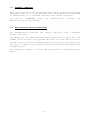
1.0
GENERAL INFORMATION ON THE SYS68K/CPU-6
The SYS68K/CPU-6 series of processor boards uses a 68000 or a 68010
CPU and the 68881 Floating Point Coprocessor (only on CPU-6VB).
To provide fast CPU operation in a local RAM area at a CPU clock
frequency of 8 or 12.5 MHz, a 512 Kbyte dynamic RAM is installed
on every CPU board. Zero or one wait state is required for each
DRAM access (8 or 12.5 MHz operation).
Three serial I/O interfaces are provided on the board to
communicate to a terminal, printer, host computer or any other
equipment which is RS232 compatible.
Up to 512 Kbytes of EPROM can be used on the four 28-pin sockets
to allow effective usage of the SYS68K/CPU-6 boards in high
performance applications.
A Real Time Clock with on-board battery backup and a parallel
interface completes the SYS68K/CPU-6.
Features of the 68000/68010
-
8
Data Registers (32 bits wide)
-
7
Address Registers (32 bits wide)
-
1
User Stack Pointer (32 bits wide)
-
1
Supervisor Stack Pointer (32 bits wide)
-
14 Addressing Modes
-
56 Powerful Instruction Types
-
16 Mbyte Direct Addressing
asynchronous Bus Interface
-
16 Bit Data Bus
1-1
Range
using
a
fully
This page was intentionally left blank
2.0
THE FLOATING POINT COPROCESSOR
The 68881 Floating Point Coprocessor (FPCP) is a full
implementation of the IEEE Standard for Binary Floating Point
Arithmetic (IEEE 754).
The FPCP instruction set supports all the addressing modes of the
68000 family. The FPCP is installed on the SYS68K/CPU-6VB as a
coprocessor with access from the 68010 via the local bus.
Features of the 68881
-
16.7 MHz clock frequency.
-
8 general purpose floating point data registers
supporting 80 bit extended precision of real data. (64
bit mantissa, 15 bit exponent, and one sign bit).
-
3 registers for control, status and instruction address.
-
67 bit arithmetic unit
-
67 bit barrel shifter
-
46 instructions with 35 arithmetic operations.
-
IEEE 754 compatible including all requirements and
suggestions.
-
Full set of trigonometric and transcended functions.
-
7 data types:
-
Byte Integer
Word Integer
Long Word Integer
Single Precision Real
Double Precision Real
Extended Precision Real
Packed Decimal Strings
-
22 constants available in the on-chip ROM, including Pi,
e, and powers of 10.
-
Virtual memory/machine operations
-
Efficient mechanism for procedure
switches and interrupt handling.
2-1
calls,
context
This page was intentionally left blank
3.0
THE MONITOR OF SYS68K/CPU-6
Every CPU-6 board contains VMEPROM, a realtime multitasking monitor
debugger.
It consists of a powerful realtime kernel, a file
manager
and
a
monitor/debugger
with
68000/68010
line
assembler/disassembler.
The monitor/debugger includes all functions to control the realtime
kernel and file manager as well as all tools required for program
debugging such as breakpoints, tracing, memory display, memory
modify and host communication.
VMEPROM supports several memory and I/O boards on the VMEbus to
take full advantage out of the file manager and the kernel
functions.
A built-in selftest checks all on-board devices together with the
on-board memory. This allows the detection of all failures on the
board.
Memory initialization and test commands offers easy installation
of global memory in the environment on the VMEbus.
The one line assembler/disassembler is 68000/68010 compatible and
supports all commands in the original mnemonic.
For reference to the I/O devices of VMEPROM please see register 8,
entitled "BIOS Source Code Listing".
3-1
This page was intentionally left blank
4.0
DEVELOPMENT SYSTEMS WITH SYS68K/CPU-6
For software development with the SYS68K/CPU-6 series of boards,
FORCE
COMPUTERS
offers
a
development/target
system
with
SYS68K/CPU-6 as a CPU board, and the Real Time Operating System
PDOS*.
The multiuser Real Time Operating System includes an Assembler for
the 68000/68010 as well as the following programming languages as
an option:
C
FORTRAN 77
PASCAL
All of these compilers generate efficient code to optimize the run
time of the programs.
Further details are listed in the data sheet of the miniFORCE
series of development/target systems.
PDOS* is a trademark of Eyring Research Laboratories.
4-1
This page was intentionally left blank
4-2
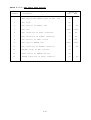
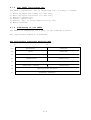
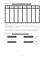
5.0
HISTORY OF MANUAL REVISIONS
REVISION
DESCRIPTION
DATE OF LAST CHANGE
Rev. 1
1. VMEPROM description for
Version 2.53 included.
NOV/28/1989
2. Chapter 6.5, "The Programmable Reset Option" has
been added.
3. Default Jumpersetting of
B23 has been corrected.
Rev. 2
Appendix F, "Front Panel
Switches", has been removed
from Section 7, "Appendix to
the Introduction to VMEPROM".
JUL/25/1990
Rev. 3
Appendix H,"Generation of
Application in EPROM" has
been removed from Section
7, "Appendix to the
Introduction to VMEPROM".
OCT/07/1992
Rev. 4
Corrected chapter 4.2.3,
"Access Time Selection"
AUG/06/1996
5-1
This page was intentionally left blank
5-2
INSTALLATION
This page was intentionally left blank
PLEASE READ THE COMPLETE INSTALLATION PROCEDURE BEFORE THE BOARD
IS INSTALLED IN A VMEBUS ENVIRONMENT TO AVOID MALFUNCTIONS AND
COMPONENT DAMAGES.
This page was intentionally left blank
TABLE OF CONTENTS
1.0
GENERAL OVERVIEW
. . . . . . . . . . . . . . . . .
1.1 The Function Switch Positions
. . . . . . . .
1.2 Connection of the Terminal . . . . . . . . . .
Page
1-1
1-1
1-3
2.0
THE DEFAULT HARDWARE SETUP
. . . . . . . . . . . .
2.1 The VMEbus Setup . . . . . . . . . . . . . . .
2.2 The Local Setup
. . . . . . . . . . . . . . .
2-1
2-1
2-2
3.0 INSTALLATION IN THE RACK
. . . . . . . . . . . . .
3.1 Power On
. . . . . . . . . . . . . . . . . . . . . . .
3.2 Correct Operation
. . . . . . . . . . . . . .
3-1
3-1
3-2
4.0
4-1
4-2
5.0
JUMPERS SETTINGS ON THE SYS68K/CPU-6
. . . . . . .
4.1 System and User I/O Jumpers
. . . . . . . . .
4.2 Jumper Location Diagram of the System and User I/O
Configuration Jumpers . . . . . . . . . . . . . .
4.3 VMEbus Configuration Jumpers . . . . . . . . .
4.4 Jumper Location Diagram of the VMEbus Configuration
Jumpers . . . . . . . . . . . . . . . . . . . . .
4.5 Local Configuration Jumpers
. . . . . . . . .
4.6 Jumper Location Diagram of the Local Configuration
Jumpers . . . . . . . . . . . . . . . . . . . . .
WARNINGS
. . . . . . . . . . . . . . . . . . . . .
4-3
4-4
4-5
4-6
4-7
5-1
LIST OF FIGURES
Figure 1-1
The Front Panel of SYS68K/CPU-6................. 1-2
This page was intentionally left blank
1.0
GENERAL OVERVIEW
Easy installation of the SYS68K/CPU-6 products is provided because
the memory map, the I/O devices and their interfaces are configured
to communicate to a standard terminal with RS232 interface.
The monitor (VMEPROM) boots
modifications to the boards.
1.1
up
automatically
without
any
The Function Switch Positions
The SYS68K/CPU-6 contains two toggle switches with a default
parking position.
The RESET and the ABORT switches move automatically back into the
"DOWN" position after having been switched into the "UP" position.
Please toggle the switch sometime before installing the board into
the rack, to detect any switches which may have been damaged during
transportation.
For reference, Figure 1-1 shows the Front Panel of SYS68K/CPU-6 in
detail.
1-1
Figure 1-1:
The Front Panel of SYS68K/CPU-6
1-2
1.2
Connection of the Terminal
The terminal must be connected to the terminal interface connector,
found in the middle of the front panel (P4).
The following communication setup is used for interfacing the
terminal:
No Parity
8 Bits per character
1 Stop Bit
9600 Baud
Asynchronous Protocol
Please configure the terminal to this setup.
The hardware interface is RS232 compatible and the following
signals are supported:
Signal
PIN
Protective
GND
1
Input
Output
RxD
2
TxD
3
x
DTR
5
x
GND
7
CTS
20
CAUTION:
Common
x
x
x
The terminal used must not drive a signal line which is
marked to be an output of SYS68K/CPU-6.
All signals marked as "Input" or "Common" have to be
supported from the terminal to enable the transmission.
If the terminal is configured to the setup listed above,
please connect the 25 pin D-sub connector to the
terminal with a cable which supports all of the listed
signals.
1-3
This page was intentionally left blank
2.0
THE DEFAULT HARDWARE SETUP
All VMEbus and local interfaces
immediately without any changes.
are
configured
to
be
used
This results in a default hardware setup which may conflict with
other boards also installed in the rack.
2.1
The VMEbus Setup
The following signals are driven/received from the SYS68K/CPU-6:
Driven
SYSCLK
x
BR3*
x
BG3OUT*
x
Received
From
Clock Module
x
Requester Logic to
Single Level Arbiter
DTB Arbitration
ACFAIL*
Local PI/T and
Jumperfield
SYSFAIL*
Local PI/T and
Jumperfield
SYSRESET*
CAUTION:
x
x
Power Monitor and
RESET Generator
The on-board single level arbiter is enabled and reacts
on every BR3*.
SYS68K/CPU-6 is configured as a slot 1 board.
2-1
2.2
The Local Setup
The local DRAM is initialized from location $8 to $4000. This area
is under the control of, and reserved for the VMEPROM firmware
which is installed on each SYS68K/CPU-6 board.
All other RAM cells (on the local DRAM and on the VMEbus) will not
be accessed and will remain unmodified. The initialization and
test of memory areas can be carried out via VMEPROM commands.
All local devices, the serial I/O interfaces, the Real Time Clock
and the PI/T are initialized after boot up.
The VMEPROM is
configured to work independent of hardware connections to the
REMOTE and HOST ports, as well as to the Parallel Interface.
All jumpers of the different SYS68K/CPU-6 board versions are set
during manufacturing so that no jumper setting change is required
in order to boot the board.
2-2
3.0
INSTALLATION IN THE RACK
All SYS68K/CPU-6 boards are preset to the default condition and can
be mounted immediately into a VME rack only at slot 1.
CAUTION:
A)
Switch off power before installing the board, to
avoid electrical damages of the components.
B)
The board contains a special ejector on the front
panel.
To ensure proper installation, the board must be
plugged in and the screws of the front panel must
be turned.
3.1
C)
Unplug every other VMEbus or VMXbus board to avoid
conflicts.
D)
Remove all connections on the P2 backplane to avoid
conflicts.
Power On
If the board is correctly installed, the switches are in the
correct positions, the terminal is correctly configured and under
power; the power for the VMEbus rack can be switched on.
First, the HALT LED must show a red light; then, after one to three
seconds, it must change to a green light.
At the same time, the following message is displayed on the
terminal:
*****************************************************************
*
*
*
V M E P R O M (TM)
*
*
*
*
SYS68K/CPU-6
Version 2.1
24-MAY-88
*
*
*
*
(c) FORCE COMPUTERS and Eyring Research
*
*
*
*****************************************************************
The next entry on the terminal keyboard may be some carriage
returns, which will result in a display of an equivalent number of
question marks (?).
3-1
3.2
Correct Operation
To test the correct operation of the CPU-6 the following command
has to be typed in:
? SELFTEST
After a matter of a few seconds, the following messages will appear
on the screen:
Memory test passed
I/O test passed
Clock test passed
Any errors will be reported as they are designated.
If an error message is displayed, please refer to register 6,
"Introduction to VMEPROM" and the command description "SELFTEST".
The next steps are under User’s direction.
3-2
4.0
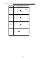
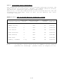
JUMPERS SETTINGS ON THE SYS68K/CPU-6
Jumper
field Coordinate
Page
Description
Jumper
field
Page
Coordinate Description
B1
1-B1
E-2
B23
7-C1
E-4
B3
1-B4
E-2
B24
7-A4
E-2
B5
1-D1
E-2
B24A
7-B3
E-2
B7
1-D3
E-2
B25
7-C3
E-6
B8
2-A1
E-6
B26
8-C3
E-6
B9
2-A3
E-6
B27
8-D3
E-6
B10
2-A2
E-6
B31
7-D2
E-6
B11
2-B4
E-6
B32
7-D2
E-6
B13
3-D1
E-4
B33
7-D3
E-6
B14
4-B3
E-4
B34
7-D3
E-6
B15
4-D1
E-4
B35
3-A2
E-6
B16
4-A4
E-6
B36
4-A2
E-4
B21
6-C2
E-6
B37
4-A1
E-4
4-1
4.1
System and User I/O Jumpers
Jumperfield
Description
Default
Schematics
See
Page
B1
Serial I/O Interface
configuration for remote
2
3
4
5
7
10
6
-
19
18
17
16
8
11
13
1 - B1
4-31
B3
Serial I/O Interface
configuration for
terminal
2
3
4
5
7
10
6
-
19
18
17
16
8
11
13
1 - B3
4-24
B5
Serial I/O Interface
configuration for host
2
3
4
5
7
8
-
15
14
13
12
10
9
1 - D1
4-38
B7
Baud Rate Control
1
3
5
10
-
20
18
16
11
1 - D3
4-17
B24
Parallel Interface
1
3
4
7
10
13
16
19
-
2
6
5
8
11
14
17
20
7 - A4
4-47
B24A
Parallel Interface
7 - B3
4-47
1 - 6
2 - 5
3 - 4
4-2
4.2
Jumper Location Diagram of the System and User I/O Configuration
Jumpers
4-3
4.3
VMEbus Configuration Jumpers
Jumperfield
Description
B14
B36
B37
B300
Reset Generator
B13
Bus Request
Bus Grant
SYSCLK
BCLR
B15
Bus IRQ enable
B23
Short I/O Address
Modifier
Default
------1 - 2
4
4
4
4
-
B3
A2
A2
B2
See
Page
6-1
2
4
6
7
8
10
11
13
14
-
3
27
25
24
9
21
20
18
17
3 - D1
5-21
1
2
3
4
5
6
7
-
14
13
12
11
10
9
8
4 - D1
5-32
7 - C1
5-9
-----------------
4-4
Schematics
4.4
Jumper Location Diagram of the VMEbus Configuration Jumpers
4-5
4.5
Local Configuration Jumpers
Jumperfield
Description
Default
Schematics
See
Page
4-83
B25
Error Timer
7 - 10
11 - 14
7 - C3
B33
Error Timer
1 - 2
7 - D3
B34
Error Timer
-
B25
Bus Mastership Timer
5 - 8
7 - C2
B31
2 - 3
7 - D2
B32
-
B8
Clock Selectors
B9
1 - 2
2 - A1
--
1 - 2
2 - A3
--
2 - A2
3-1
2 - B4
4-14
B10
8MHz
2 - 3
4 - 5
B10
12.5MHz
1 - 2
5 - 6
B11
EPROM Access Time
Selection
B26
EPROM Size Selection
1 - 8
4 - 5
B27
B21
DTACK Generated
for RAM
B16
B35
8MHz
12.5MHz
5-21
1
10
4
7
- 12
- 11
- 9
- 8
8 - C3
4-2
1
3
4
6
- 12
- 10
- 9
- 7
8 - D3
4-8
1 - 5
4 - 5
6 - C2
3-1
Battery (STDBY)
-
4 - A4
4-56
Read-Modify-Write
-
3 - A2
--
4-6
4.6
Jumper Location Diagram of the Local Configuration Jumpers
4-7
This page was intentionally left blank
5.0
WARNINGS
A)
If the board does not boot up correctly, please do not remove
any jumpers.
B)
If an error has been found by VMEPROM, please refer to the
VMEPROM User’s Manual for a detailed error description.
C)
If the terminal does not display the described text, the
terminal setup may be wrong. Please check this setup.
D)
If the board does not boot up correctly, please do not place
the board back into the plastic box without replacing the metal
foil on the back or putting the board into an antistatic bag,
or components may be destroyed.
E)
Please do not install other VMEbus boards into a rack which
includes the following functions, before the jumper settings
have been changed: SYSCLK Driver, Arbiter.
F)
Please do not solder the battery (included in the shipment)
into the PCB prior to reading the installation paragraph, and
prior to testing the board functions with the SELFTEST command.
G)
Please do not connect I/O signals at P2 connector prior to
cross checking the SYS68K/CPU-6 P2 I/O signal assignment to
avoid component damages.
H)
The RESET instruction of the local CPU does not reset the local
I/O devices, only the VMEbus SYSRESET will be forced if the
jumper setting is in the default condition.
5-1
SYS68K/CPU-6
HARDWARE USER’S MANUAL
This page was intentionally left blank
TABLE OF CONTENTS
1.0
GENERAL INFORMATION
2.0
HARDWARE OVERVIEW
3.0
THE 68000/68010 MICROPROCESSOR DESCRIPTION
3.1 The 68000 Hardware Description . . .
3.2 The Vector Table of the 68000
. . .
3.3 The 68010 Hardware Description . . .
3.4 The Vector Table of the 68010
. . .
3.5 The Address Map of SYS68K/CPU-6
. .
4.0
. . . . . . . . . . . . . . . .
1-1
. . . . . . . . . . . . . . . . .
2-1
.
.
.
.
.
.
.
.
.
.
.
.
.
.
.
.
.
.
.
.
.
.
.
.
.
.
.
.
.
THE LOCAL BUS . . . . . . . . . . . . . . . . . . .
4.1 EPROM Area 1 . . . . . . . . . . . . . . . . .
4.1.1 Memory Organization of EPROM Area 1
4.1.2 Usable Device Types of EPROM Area 1
4.1.3 Access Timer Selection of EPROM Area 1
. . . . . . . . . . . . . . . . . . . . .
4.1.4 Insertion of Devices into EPROM Area 1
. . . . . . . . . . . . . . . . . . . . .
4.1.5 Address Map of EPROM Area 1
. . .
4.1.6 Summary of EPROM Area 1
. . . . .
4.2 The EPROM Area 2 . . . . . . . . . . . . . . .
4.2.1 Memory Organization of EPROM Area 2
4.2.2 Usable Device Types
. . . . . . .
4.2.3 Access Time Selection
. . . . . .
4.2.4 Address Map of EPROM Area 2
. . .
4.2.5 The USER Area Summary
. . . . . .
4.3 The Serial I/O Interfaces
. . . . . . . . . .
4.3.1 The Baud Rate Selection
. . . . .
4.3.2 Timing of the ACIAs
. . . . . . .
4.3.3 The Terminal Port
. . . . . . . .
4.3.3.1 The I/O Signal Assignment
4.3.3.2 Register Layout
. . .
4.3.3.3 Baud Rate Selection
.
4.3.3.4 Terminal Port Summary
4.3.4 The Remote Port
. . . . . . . . .
4.3.4.1 The I/O Signal Assignment
. . . . . . . . . . . . . . . .
4.3.4.2 Register Layout
. . .
4.3.4.3 Baud Rate Selection
.
4.3.4.4 Remote Port Summary
.
4.3.5 The Host Port
. . . . . . . . . .
4.3.5.1 The I/O Signal Assignment
. . . . . . . . . . . . . . . .
4.3.5.2 Register Layout
. . .
4.3.5.3 Baud Rate Selection
.
4.3.5.4 Host Port Summary
. .
4.4 The Parallel Interface and Timer Chip
. . . .
4.4.1 The PI/T Register Layout and Addressing
. . . . . . . . . . . . . . . . . . . . .
4.4.2 The Timer
. . . . . . . . . . . .
4.4.3 Interrupt Handling . . . . . . . .
4.4.4 Summary of the PI/T
. . . . . . .
4.5 The Real Time Clock
. . . . . . . . . . . . .
4.5.1 Register Layout
. . . . . . . . .
4.5.2 Access Timing
. . . . . . . . . .
4.5.3 The Battery Backup Mode
. . . . .
4.5.4 The Interrupt Assignment . . . . .
4.5.5 Summary of the RTC . . . . . . . .
3-1
3-4
3-5
3-6
3-8
3-9
4-1
4-1
4-1
4-1
4-6
4-6
4-6
4-7
4-8
4-8
4-8
4-14
4-16
4-16
4-17
4-17
4-22
4-25
4-25
4-31
4-31
4-31
4-32
4-32
4-37
4-37
4-38
4-39
4-42
4-47
4-47
4-47
4-48
4-50
4-50
4-55
4-55
4-56
4-57
4-57
4-57
4-63
4-63
TABLE OF CONTENTS (cont’d)
4.6
4.7
4.8
4.9
5.0
6.0
The Dynamic RAM
. . . . . . . . . . . . .
4.6.1 Address Map and Capacity . . .
4.6.2 Access Timing of the DRAM
. .
4.6.3 Refreshing of the DRAMs
. . .
4.6.4 The Summary of the DRAM
. . .
The Floating Point Coprocessor 68881 (FPCP)
4.7.1 Interfacing to the 68881 . . .
4.7.2 The Data Format of the 68881 .
4.7.3 The 68881 Instruction Set
. .
4.7.4 Addressing of the 68881
. . .
4.7.5 Detection of the 68881 . . . .
4.7.6 RESET of the FPCP
. . . . . .
4.7.7 Summary of the 68881 . . . . .
Local Interrupt Handling . . . . . . . . .
4.8.1 Interrupt Level Assignment . .
4.8.2 Usage of the Auto Vectors
. .
4.8.3 Summary of the Local Interrupts
The BERR Generator . . . . . . . . . . . .
.
.
.
.
.
.
.
.
.
.
.
.
.
.
.
.
.
.
.
.
.
.
.
.
.
.
.
.
.
.
.
.
.
.
THE VMEbus INTERFACE
. . . . . . . . . . . . . . .
5.1 Data Transfer Size . . . . . . . . . . . . . .
5.2 The Address Modifier Implementation
. . . . .
5.2.1 The Short I/O Address Modifier Code
5.3 The VMEbus Arbitration
. . . . . . . . . . .
5.3.1 The Arbiter Options
. . . . . . .
5.3.2 The On-Board DTB Slave Bus Arbitration
. . . . . . . . . . . . . . . . . . . . .
5.4 The Single Level Bus Arbiter . . . . . . . . .
5.5 VMEbus Release Functions . . . . . . . . . . .
5.5.1 Release On Request (ROR) . . . . .
5.5.2 Release on Bus Clear (RBCLR) . . .
5.5.3 Release After Time-Out (RAT) . . .
5.6 The Slot 1 Functions . . . . . . . . . . . . .
5.6.1 The SYSCLK Driver
. . . . . . . .
5.6.2 ACFAIL . . . . . . . . . . . . . .
5.6.3 SYSFAIL
. . . . . . . . . . . . .
5.7 The VMEbus Interrupt Handler . . . . . . . . .
5.7.1 The On-Board IACK Daisy Chain
. .
5.7.2 The VMEbus Interrupt Handling
. .
5.7.3 The ABORT Function Switch
. . . .
5.8 Summary of the VMEbus Interface
. . . . . . .
THE RESET STRUCTURE . . . . . . . . .
6.1 The Voltage Sensor . . . . . . .
6.3 The Reset Instruction of the CPU
6.4 The Reset Function Switch
. . .
6.5
The Programmable Reset Option
6.6
The Run/Halt Indication LED
.
.
.
.
.
.
.
.
.
.
.
.
.
.
.
.
.
.
.
.
.
.
.
.
4-65
4-65
4-65
4-68
4-70
4-71
4-72
4-73
4-76
4-76
4-77
4-77
4-77
4-78
4-80
4-81
4-83
4-84
5-1
5-1
5-7
5-9
5-12
5-12
5-15
5-20
5-21
5-21
5-21
5-21
5-24
5-24
5-24
5-24
5-26
5-26
5-32
5-36
5-36
.
.
.
.
6-1
6-1
6-2
6-3
. . . . . . . .
6-3
. . . . . . . . .
6-6
List of Figures
Figure 1-1:
Figure 1-2:
Photo of SYS68K/CPU-6 . . . . . . . . . .
Block Diagram of the SYS68K/CPU-6 . . . .
1-2
1-3
Figure 3-1:
Figure 3-2:
CPU-Clock Speed Jumper Settings . . . . .
Location Diagram of the CPU Clock Speed
Jumperfields B10 and B21 . . . . . .
3-2
Figure
Figure
Figure
Figure
Figure
Figure
4.0-1:
4.1-2:
4.1-3:
4.2-1:
4.2-2:
4.3-1:
Figure
Figure
Figure
Figure
Figure
Figure
Figure
Figure
4.3-4:
4.3-5:
4.3-6:
4.3-7:
4.3-8:
4.3-9:
4.3-10:
4.3-11:
Figure
Figure
Figure
Figure
Figure
Figure
Figure
Figure
Figure
Figure
Figure
Figure
Figure
Figure
4.3-12:
4.3-13:
4.4-1:
4.4-2:
4.5-1:
4.5-2:
4.5-3:
4.6-1:
4.6-2:
4.7-1:
4.7-2:
4.8-1:
4.9-1:
4.9-2:
Block Diagram of SYS68K/CPU-6 . . . . . .
Location Diagram of the EPROM Area 1
. .
Location Diagram of the Jumperfield B26 .
Location Diagram of the EPROM Area 2
. .
Location Diagram of the Speed Selectors .
Hardware Drawing of the Baud Rate Selection
Parts
. . . . . . . . . . . . . . .
Default Jumper Settings of B7
. . . . .
Location Diagram of the Baud Rate Selection
Parts
. . . . . . . . . . . . . . .
ACIA Timing Diagram (best case) . . . . .
ACIA Timing Diagram (worst case)
. . . .
Hardware Diagram of the Terminal Port . .
Location Diagram of the Terminal Port . .
Hardware Diagram of the Remote Port . . .
Location Diagram of the Remote Port . . .
Configuration with a Host Computer
. . .
Interfacing to a Host Computer in the
Transparent Mode
. . . . . . . . . . . .
Hardware Diagram of the Host Port . . . .
Location Diagram of the Host Port . . . .
The Hardware Diagram of the PI/T
. . . .
The Location Diagram of the PI/T
. . . .
RTC Write Cycle Timing Diagram
. . . . .
RTC Read Cycle Timing Diagram . . . . . .
The Location Diagram of the RTC . . . . .
Access Cycle without Refresh Request
. .
The Global Refresh Timing Diagram . . . .
Data Format Summary of the 68881
. . . .
Register Model of the 68881 . . . . . . .
The Global Interrupt Vector Acquisition .
Timing Diagram of a BERR Cycle
. . . . .
Location Diagram of the BERR Jumperfield
Figure
Figure
Figure
Figure
Figure
Figure
Figure
Figure
5.1-1:
5.1-2:
5.2-1:
5.2-2:
5.3-1:
5.3-2:
5.3-3:
5.3-4:
Read Cycle Followed by Write Cycle
. .
Write Cycle Followed by Read Cycle
. .
The Short I/O Comparator
. . . . . . .
Location Diagram of the Short I/O Parts
The Bus Grand Daisy Chain . . . . . . .
Global DTB Arbitration Timing . . . . .
Bus Arbitration Timing Diagram
. . . .
The Jumperfield for the Bus Arbitration
Figure 4.3-2:
Figure 4.3-3:
.
.
.
.
.
.
.
.
3-3
4-2
4-3
4-5
4-12
4-15
5-3
5-5
5-9
5-11
5-13
5-14
5-16
5-17
4-19
4-20
4-21
4-23
4-24
4-26
4-30
4-33
4-34
4-40
4-41
4-44
4-46
4-49
4-54
4-60
4-62
4-64
4-67
4-69
4-74
4-75
4-82
4-85
4-88
List of Figures (cont’d)
Figure 5.3-5:
Figure 5.3-6:
Figure 5.5-1:
Figure 5.6-2:
Figure 5.7-1:
Figure 5.7-2:
Figure 5.7-3:
Figure 5.7-4:
Figure 5.7-5:
Figure 6.4-1:
Figure 6.4-2:
Arbiter and Bus Request Level Jumper Selection
on B13 with External Arbiter
. . . . . .
5-18
The Location Diagram of the Slave Bus
Arbitration . . . . . . . . . . . . . . .
5-19
Location Diagram of the RAT Jumperfield .
5-23
Location Diagram of the Special Function
Jumpers . . . . . . . . . . . . . . . . .
5-25
The Interrupt Acknowledge Daisy Chain . .
5-27
Functional
Diagram
of
the
Interrupt
Acknowledge
. . . . . . . . . . . . . .
5-28
The Interrupt Vector Acquisition Timing
Diagram . . . . . . . . . . . . . . . . .
5-31
The VMEbus Interrupt Hardware Diagram . .
5-33
Location Diagram of the VMEbus Interrupt Parts
. . . . . . . . . . . . . . . . . . . . .
5-35
The Location Diagram of the Reset Signal
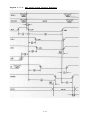
The Front Panel of the CPU-6
. . . . . .
6-4
6-5
List of Tables
Table 3-1:
Table 3.5-1:
CPU-Clock Frequency . . . . . . . . . . .
Memory Map of SYS68K/CPU-6
. . . . . . .
3-1
3-10
Table
Table
Table
Table
Table
Table
Table
Table
Table
Table
Table
Table
Table
Table
Table
Table
Table
Table
Table
Table
Table
4.1-1:
4.1-2:
4.2-1A:
4.2-1B:
4.2-2:
4.2-3:
4.3-1:
4.3-2:
4.3-3:
4.3-4:
4.3-5:
4.3-6:
4.3-7:
4.3-8:
4.3-9:
4.4-1:
4.4-2:
4.5-1:
4.5-2:
4.5-3:
4.6-1:
4-4
4-6
4-10
4-11
4-14
4-16
4-17
4-22
4-22
4-27
4-29
4-35
4-36
4-43
4-45
4-51
4-53
4-58
4-59
4-61
Table
Table
Table
Table
Table
Table
Table
Table
4.8-1:
4.8-2:
4.8-3:
4.8-4:
4.9-1:
4.9-2:
4.9-3:
4.9-4:
EPROM Area 1 Jumper Settings
. . . . . .
Address Map of EPROM Area 1 . . . . . . .
EPROM Area 2 Jumper Settings for EPROMs .
EPROM Area 2 Jumper Settings for SRAMs
.
EPROM Speed Selection . . . . . . . . . .
Address Map of EPROM Area 2 . . . . . . .
The Baud Rate Selection Jumper B7
. . .
ACIA Timing (best case) . . . . . . . . .
ACIA Timing (worst case)
. . . . . . . .
Terminal Connector Signal Assignments . .
Default Jumper Setting at B3
. . . . . .
Remote Connector Signal Assignments . . .
Default Jumper Settings at B1 . . . . . .
Host Signal Assignments . . . . . . . . .
Default Jumper Settings at B5 . . . . . .
The PI/T Address Map
. . . . . . . . . .
Default Jumper Settings for B24 and B24A
Register Model of the RTC . . . . . . . .
RTC Write Time Values . . . . . . . . . .
RTC Read Time Values
. . . . . . . . . .
Time Values for an Access Cycle without
Refresh Request . . . . . . . . . . . . .
The Interrupt Acknowledge Level Code
. .
The Interrupt Vector Conversion . . . . .
The On-Board Devices Interrupt Scheme . .
The Autointerrupt Vector Table
. . . . .
BERR Jumper Settings A
. . . . . . . . .
BERR Jumper Settings B
. . . . . . . . .
BERR Jumper Settings C
. . . . . . . . .
BERR Jumper Settings D
. . . . . . . . .
Table
Table
Table
Table
Table
Table
Table
5.1-1:
5.1-2:
5.2-1:
5.2-2:
5.4-1:
5.5-1:
5.7-1:
Read Cycle followed by Write Cycle
. . .
Write Cycle followed by Read Cycle
. . .
The Address Modifier Codes
. . . . . . .
The Short I/O Jumper Settings . . . . . .
Time Values of the Single Level Bus Arbiter
Jumper Settings of B25, B31 and B32 for RAT
Time
Values
of
the
Interrupt
Vector
Acquisition . . . . . . . . . . . . . . .
The VMEbus Interrupt Jumper Settings
. .
5-2
5-4
5-8
5-10
5-20
5-22
Table 5.7-2:
4-66
4-79
4-79
4-80
4-81
4-86
4-86
4-87
4-87
5-30
5-34
This page was intentionally left blank
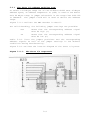
1.0
GENERAL INFORMATION
The SYS68K/CPU-6 series of processor boards combines the powerful
16/32 bit microprocessor, the 68000/68010 with 512 Kbytes of
dynamic RAM and a VMEbus interface.
The on-board Real Time Clock, the three serial I/O interfaces and
the parallel I/O and timer offer a powerful combination to
accomplish a wide variety of applications.
Easy access to the installed devices is provided through the ROM
resident monitor called VMEPROM. This powerful software package
is based on a realtime kernel and file manager and can be used for
program development and debugging of application programs.
The usage of the SYS68K/CPU-6 series of boards in critical real
time applications is provided through the high CPU clock rate (up
to 12.5 MHz) and the fast on-board DRAM (only 1 wait state at
12.5 MHz).
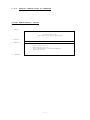
1-1
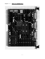
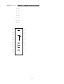
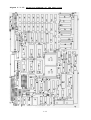
Figure 1-1:
Photo of SYS68K/CPU-6
1-2
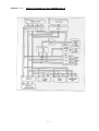
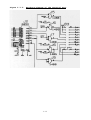
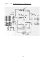
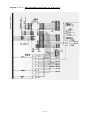
Figure 1-2:
Block Diagram of the SYS68K/CPU-6
1-3
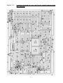
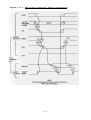
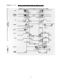
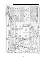
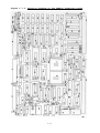
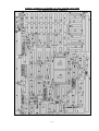
2.0
HARDWARE OVERVIEW
The SYS68K/CPU-6 boards contain the powerful 68000/68010 CPU with
512 Kbytes of dynamic RAM, a maximum of 256 Kbytes of EPROM and
powerful I/O devices.
One RS232 interface (Port 2 connector P4) is used in conjunction
with a standard terminal to enter and debug user programs under the
control of VMEPROM. A second RS232 interface (Port 1 connector P3)
may be used for up/download of user programs and data. The third
RS232 interface (Port 3 connector P5) is a universal port to
support an additional terminal, printer or other device.
A Parallel Interface and Timer Chip (PI/T 68230) is used to
interface various hardware on the P2 connector and to work as the
time base for VMEPROM.
In addition, the Real Time Clock (RTC 58167A) provides a constant
time base because of its on-board battery backup.
The SYS68K/CPU-6VB contains a Floating Point Coprocessor
(FPCP 68881) with 12.5 MHz clock rate to support floating point
applications.
All of the I/O devices, the DRAM, and the EPROM areas are located
on the local bus. Memory and I/O extension is provided using the
VMEbus interface.
The block diagram of SYS68K/CPU-6 shows the
functional areas in detail.
2-1
This page was intentionally left blank
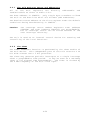
3.0
THE 68000/68010 MICROPROCESSOR DESCRIPTION
The 68000/68010 contains seventeen 32 bit registers, two 32 bit
program counters and a 16 bit status register.
The first eight registers are used as data registers (D0-D7) for
byte (8 bit), word (16 bit), and long word (32 bit) operations.
The seven address registers (A0-A6), the supervisor, and the user
stack pointer may be used as base address registers or as software
stack pointers, where word and long word operations are supported.
All of the 17 registers described may be used for word and for long
word address operations or as index registers.
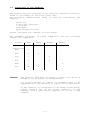
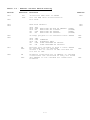
Table 3-1 lists the clock frequencies for each of the SYS68K/CPU-6
versions, the processor type, and the corresponding jumper
settings.
Table 3-1:
CPU-Clock Frequency
Version
CPU Type
Clock Frequency
CPU-6A
68000
12.5 MHz
Mode A
CPU-6V
68010
8.0 MHz
Mode B
CPU-6VA
68010
12.5 MHz
Mode A
CPU-6VB
68010
12.5 MHz
Mode A
3-1
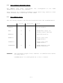
Jumper Settings at B10
Figure 3-1:
CPU Clock Speed Jumper Settings
Mode A
CPU-6A
CPU-6VA
CPU-6VB
B21
1
B10
o
o
o
o
o
o
Mode B
1
o
o
o
o
o
o
o
o
o
o
o
o
CPU-6V
B21
B10
o
o
o
/
1
o
Caution:
o
o
1
No other jumper settings are allowed. Any other jumper
setting than those shown can cause component damage
and/or other malfunctions.
3-2
Figure 3-2:
Location Diagram of the CPU Clock Speed Jumperfields
B10 and B21
3-3
3.1
The 68000 Hardware Description
The 68000 provides 23 address signals, 16 data signals and 10
control signals which build the fully asynchronous bus interface.
A Data Transfer Acknowledge (DTACK) and a Bus Error (BERR) input
signals the CPU if a bus cycle can be aborted correctly or if an
error has been detected.
Seven interrupt request signals are encoded and driven to the CPU
to provide fast and effective interrupt acknowledgment for real
time applications.
Features of the 68000
-
8 data registers (32 bit)
-
7 address registers (32 bit)
-
32 bit supervisor stack pointer
-
32 bit user stack pointer
-
16 bit status register
-
16 Mbyte direct addressing space
-
Hardware signals provide detection of program and data
fetches, as well as of supervisor and user mode
-
56 powerful instruction types with 14 addressing modes
-
5 main data types
-
Memory mapped I/O
-
Asynchronous bus interface
3-4
3.2
The Vector Table of the 68000
Vector
No.(s)
Address
Hex
Dec
Space
Assignment
0
0
000
SP
Reset:Initial SSP
-
4
004
SP
Reset:Initial PC
2
8
008
SD
Bus Error
3
12
00C
SD
Address Error
4
16
010
SD
Illegal Instruction
5
20
014
SD
Zero Divide
6
24
018
SD
CHK Instruction
7
28
01C
SD
TRAPV Instruction
8
32
020
SD
Privilege Violation
9
36
024
SD
Trace
10
40
028
SD
Line 1010 Emulator
11
44
02C
SD
Line 1111 Emulator
12*
13*
14*
15
48
52
56
60
030
034
038
03C
SD
SD
SD
SD
(Unassigned,reserved)
(Unassigned,reserved)
(Unassigned,reserved)
Uninitialized Interrupt
16-23
64
04C
SD
Vector
(Unassigned,reserved)
95
05F
24
96
060
SD
Spurious Interrupt
25
100
064
SD
Level 1 Interrupt
-
Autovector
26
104
068
SD
Level 2 Interrupt
Autovector
27
108
06C
SD
Level 3 Interrupt
Autovector
3-5
The Vector Table of the 68000 cont.
Vector
No.(s)
28
Dec
112
Address
Hex
070
Space
Assignment
SD
Level 4 Interrupt
Autovector
29
116
074
SD
Level 5 Interrupt
Autovector
30
120
078
SD
Level 6 Interrupt
Autovector
31
124
07C
SD
Level 7 Interrupt
Autovector
32-47
128
080
SD
TRAP Instruction Vectors
48-63*
191
192
255
256
0BF
0C0
0FF
100
SD
(Unassigned,reserved)
User Interrupt Vectors
1023
3FF
64-255
SD
-
*
Vector numbers 12,13,14,16 through 23, and 48 through 63 are
reserved for future enhancements. No user peripheral devices
should be assigned these numbers.
3.3
The 68010 Hardware Description
The 68010 contains the same features as those in
description
in
paragraph
3.1,
except
for
the
enhancements.
the 68000
following
A vector base register is used to determine the location of the
exception vector table in memory to support multiple vector tables
and to allow a variable memory map.
On SYS68K/CPU-6 VMEPROM, the vector base register is not altered,
which results in the same address map as used for the 68000
version.
The Function Code Register allows the supervisor to access user
data and program space to emulate CPU space cycles and/or modify
data.
3-6
During a Bus Error exception processing sequence, the following
information is placed on the supervisor stack:
A)
Status Register
B)
Program Counter (2 to 5 words)
C)
Frame format and vector offset
D)
Internal register information (22 words)
Storage of this information allows recovery from a bus error and
enables the program to be continued from where the bus error
occurred.
3-7
3.4
The Vector Table of the 68010
Vector
No.(s)
Address
Hex
Dec
Space
Assignment
0
0
000
SP
Reset:Initial SSP
-
4
004
SP
Reset:Initial PC
2
8
008
SD
Bus Error
3
12
00C
SD
Address Error
4
16
010
SD
Illegal Instruction
5
20
014
SD
Zero Divide
6
24
018
SD
CHK Instruction
7
28
01C
SD
TRAPV Instruction
8
32
020
SD
Privilege Violation
9
36
024
SD
Trace
10
40
028
SD
Line 1010 Emulator
11
44
02C
SD
Line 1111 Emulator
12*
13*
14*
15
48
52
56
60
030
034
038
03C
SD
SD
SD
SD
(Unassigned,reserved)
(Unassigned,reserved)
(Unassigned,reserved)
Uninitialized Interrupt
16-23
64
04C
SD
Vector
(Unassigned,reserved)
95
05F
24
96
060
SD
Spurious Interrupt
25
100
064
SD
Level 1 Interrupt
-
Autovector
26
104
068
SD
Level 2 Interrupt
Autovector
27
108
06C
SD
Level 3 Interrupt
Autovector
3-8
(cont’d).....
Vector
No.(s)
28
Dec
112
Address
Hex
070
Space
Assignment
SD
Level 4 Interrupt
Autovector
29
116
074
SD
Level 5 Interrupt
Autovector
30
120
078
SD
Level 6 Interrupt
Autovector
31
124
07C
SD
Level 7 Interrupt
Autovector
32-47
128
080
SD
TRAP Instruction Vectors
48-63*
191
192
255
256
0BF
0C0
0FF
100
SD
(Unassigned,reserved)
User Interrupt Vectors
1023
3FF
64-255
SD
-
*
Vector numbers 12,13,14,16 through 23, and 48 through 63 are
reserved for future enhancements. No user peripheral devices
should be assigned these numbers.
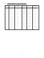
3.5
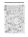
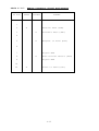
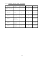
The Address Map of SYS68K/CPU-6
The memory map of SYS68K/CPU-6 is outlined in Table 3.5-1.
All memory and I/O areas are identical for all SYS68K/CPU-6
products except for the memory map of the Floating Point CoProcessor. A bus error will be generated on SYS68K/CPU-6A, 6V and
6VA if an access to the not installed FPCP is initiated.
To detect the end of the onboard DRAM area via software, the
addresses $80000 to $80007 are not decoded, and a bus error will
occur.
3-9
Table 3.5-1: Memory Map of SYS68K/CPU-6
000 000
:
000 007
ROM Initialization Vectors from SYSTEM EPROM
000 008
:
07F FFF
On-Board DRAM
080 008
:
09F FFF
SYSTEM EPROM Area (128 Kbytes)
0A0 000
:
0BF FFF
USER EPROM Area
(128 Kbytes) or SRAM (64 Kbytes)
0C0 041
:
0C0 043
RS 232 Interface
(Host)
P3 connector
0C0 080
:
0C0 082
RS 232 Interface
(Terminal)
P4 connector
0C0 101
:
0C0 103
RS 232 Interface
(Remote)
P5 connector
0C0 401
:
0C0 42F
RTC
(Real Time Clock)
0E0 001
:
0E0 035
PI/T
(Parallel Interface/Timer)
0E0 200
:
0E0 300
0E0 380
FPCP
(Floating Point Coprocessor)
Reset off
Reset on
100 000
:
FEF FFF
VMEbus (A24:D16, D8)
FF0 000
:
FFF FFF
VMEbus (A16:D16, D8)
(512 Kbytes)
3-10
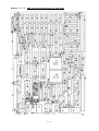
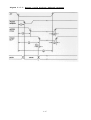
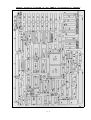
4.0
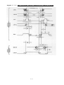
THE LOCAL BUS
Each of the SYS68K/CPU-6 products contains a local bus driven and
controlled only by the 68000/68010 CPU.
All of the memory, the I/O devices and the FPCP communicate to the
CPU via this bus.
The VMEbus interface, described in Chapter 5 of this manual is also
connected to this local bus and fully controlled by the CPU.
Detailed information about the functional groups is given in the
subsequent chapters.
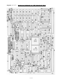
For reference, a block diagram of the
SYS68K/CPU-6 is provided at Figure 4.0-1.
The SYS68K/CPU-6 consists of four sockets for JEDEC compatible
devices. Two different memeory banks (with two sockets each) are
used; one for boot up, and one for user application programs.
4.1
EPROM Area 1
During the power up phase, the 68000 CPU reads two vectors from
this EPROM area; one is the Initial Stack Pointer (Address
$000000 - $000003) and one is the Initial Program Counter (Address
$000004 - $000007).
The data signals D0-D7 are used on the socket J75 (Lower byte) and
the data signals D8-D15 are connected to the socket J76 (Upper
byte).
4.1.1
Memory Organization of EPROM Area 1
For proper initialization, the first eight addresses of EPROM Area
1 are downmapped to address $0 to $8.
Figure 4.1-2 shows the location diagram of the EPROM Area 1.
4.1.2
Usable Device Types of EPROM Area 1
EPROM Area 1 can be configured for the listed device types if the
connections described in Table 4.1-1 are made.
Device
EPROM
EPROM
EPROM
EPROM
2764
27128
27256
27512
Organization
8K
16K
32K
64K
x
x
x
x
4-1
8
8
8
8
Capacity
16
32
64
128
Kbytes
Kbytes
Kbytes
Kbytes
total
total
total
total
Figure 4.0-1:
Block Diagram of SYS68K/CPU-6
4-2
Figure 4.1-2:
Location Diagram of the EPROM Area 1
4-3
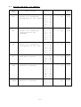
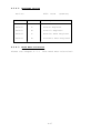
Table 4.1-1:
EPROM Area 1 Jumper Settings
Type
Jumper B26
12
o
2732
11
o
10
o
9
o
8
o
7
o
\
o
1
o
2
o
3
o
4
o
5
o
6
12
o
11
o
10
o
9
o
8
o
7
o
o
1
o
2
o
3
o
4
o
5
o
6
12
o
11
o
10
o
9
o
8
o
7
o
o
1
o
2
o
3
o
4
o
5
o
6
12
o
11
o
10
o
9
o
8
o
7
o
o
1
o
2
o
3
o
4
o
5
o
6
12
o
11
o
10
o
9
o
8
o
7
o
o
1
o
2
o
3
o
4
o
5
o
6
2764
27128
27256
27512 *
*
Default condition during manufacturing
4-4
Figure 4.1-3:
Location Diagram of the Jumperfield B26
4-5
4.1.3
Access Timer Selection of EPROM Area 1
To enable the use of fast and slow devices, the EPROM areas have
a selectable access time.
This jumperfield provides different jumper settings as listed in
Table 4.2-2.
Figure 4.2-2 shows the location diagram of the speed selectors.
4.1.4
Insertion of Devices into EPROM Area 1
The SYS68K/CPU-6 contains two 28-pin DIP sockets. The assignment
is shown in Appendix D of this manual (Register 4).
4.1.5
Address Map of EPROM Area 1
The start address of the EPROM Area 1 is fixed mapped via a
decoding PAL. The size of the memory area depends on the memory
capacity of the used devices.
Table 4.1-2 lists the address map for the different usable device
types.
Table 4.1-2: Address Map of EPROM Area 1
Start
Address
End
Address
Used
Device
Total
Capacity
080 008
083 FFF
2764
16K Byte
080 008
087 FFF
27128
32K Byte
080 008
08F FFF
27256
64K Byte
080 008
09F FFF
27512
128K Byte
4-6
4.1.6
Summary of EPROM Area 1
Start Address
End Address
$080008
$09FFFF
Boundary
$020000
Boot Address
$000000 to $000007
Access Modes
Byte or Word Read Only accesses supported
Default Access Time
250ns (max)
4-7
4.2
The EPROM Area 2
For user application programs or as a static RAM area, two 28 pin
sockets are provided on the board.
4.2.1
Memory Organization of EPROM Area 2
The chip selection for the upper (D8-D15) and the lower socket
(D0-D7) on the board is organized by byte.
This allows byte
manipulation if SRAM chips are installed.
Figure 4.2-1 shows the location diagram of the user area and the
jumper configuration area.
This jumper configuration area defines which
signals are connected to the socket pairs.
4.2.2
address/control
Usable Device Types
The following device types are usable in User Area 2:
Device
Organization
EPROM
EPROM
EPROM
EPROM
2764
27128
27256
27512
8K
16K
32K
64K
SRAM
SRAM
6264
62256
8K * 8
32K * 8
Table 4.2-1 describes
different devices.
the
*
*
*
*
8
8
8
8
jumper
4-8
Capacity
16
32
64
128
Kbytes
Kbytes
Kbytes
Kbytes
total
total
total
total
16 Kbytes total
64 Kbytes total
settings
required
for
the
This page was intentionally left blank
Table 4.2-1A:
EPROM Area 2 Jumper Settings for EPROMs
Type
Jumperfield B27
12
o
o
o
o
o
o
o
1
o
o
o
o
o
12
o
11
o
10
o
9
o
8
o
7
o
o
1
o
2
o
3
o
4
o
5
o
6
12
o
11
o
10
o
9
o
8
o
7
o
o
1
o
2
o
3
o
4
o
5
o
6
12
o
11
o
10
o
9
o
8
o
7
o
o
1
o
2
o
3
o
4
o
5
o
6
2764
27128
/
27256
*
27512
*
Default condition during manufacturing
4-10
Table 4.2-1B:
EPROM Area 2 Jumper Settings for SRAMs
No battery backup for the SRAMs
Type
Jumperfield B27
12
o
11
o
10
o
9
o
8
o
7
o
o
1
o
2
o
3
o
4
o
5
o
6
12
o
11
o
10
o
9
o
8
o
7
o
o
1
o
2
o
3
o
4
o
5
o
6
6264
62256
With on-board battery backup for the SRAMs
Type
Jumperfield B27
12
o
11
o
10
o
9
o
8
o
7
o
o
1
o
2
o
3
o
4
o
5
o
6
12
o
11
o
10
o
9
o
8
o
7
o
o
1
o
2
o
3
o
4
o
5
o
6
62LP64
62LP256
Note:
If the on-board battery backup is used, only full CMOS
devices may be installed. Otherwise, the battery will
be destroyed.
4-11
Figure 4.2-1:
Location Diagram of the EPROM Area 2
4-12
This page was intentionally left blank
4.2.3
Access Time Selection
To enable the use of fast and slow devices, the PROM/EPROM areas
have a selectable access time speed selector.
This jumperfield provides different jumper settings, as listed in
Table 4.2-2. Figure 4.2-2 shows the location diagram of the speed
selectors.
Table 4.2-2:
*
EPROM Speed Selection
Jumper
Closed
on B11
Jumper
Closed
on B11
Access Times
(ns)
Min.
Max.
7 - 8
2 - 3
62
125
60
7 - 8
4 - 5
125
188
125
7 - 8
3 - 6
188
250
180
1 - 8
2 - 3
125
250
125
1 - 8
4 - 5
250
375
250
1 - 8
3 - 6
375
500
375
Default connection at:
Device
Access
Times (ns)
Jumper B11
5
o
o
4
6
o
o
3
7
o
o
2
8
o
o
1
4-14
*
Figure 4.2-2:
Location Diagram of the Speed Selectors
4-15
4.2.4
Address Map of EPROM Area 2
The start address of the EPROM Area 2 is fixed mapped via a
decoding PAL. The size of this memory area depends on the memory
capacity of the used devices.
Table 4.2-3 lists the address map for the different usable device
types.
Table 4.2-3:
4.2.5
Address Map of EPROM Area 2
Start
Address
End
Address
Used
Device
Total
Capacity
0A0 000
0A3 FFF
2764
16 Kbytes
0A0 000
0A7 FFF
27128
32 Kbytes
0A0 000
0AF FFF
27256
64 Kbytes
0A0 000
0BF FFF
27512
128 Kbytes
0A0 000
0A3 FFF
6264
16 Kbytes
0A0 000
0AF FFF
62256
64 Kbytes
The USER Area Summary
Start Address
$0A0000
End Address
$0BFFFF
Boundary
$020000
Access Modes
Byte or Word transfers
Read or Write on SRAM
Read only on EPROM
Usable Data Bits
D0-D7 and D8-D15
Default Access Time
250ns (max)
4-16
4.3
The Serial I/O Interfaces
The board contains three independent serial I/O channels with a
separate strap selectable baud rate (110 to 38400 Baud).
Each
serial I/O interface has a jumperfield for easy I/O signal
assignment changes to the 25 pin D-sub connectors (female).
All serial I/O control chips are 6850
Communication Interface Adapter - ACIA).
4.3.1
devices
(Asynchronous
The Baud Rate Selection
Each clock input for the transmit and receive baud rate of the
three serial I/O channels is strap selectable to one of the nine
different baud rate clocks driven by the 14411. The jumperfield
B7 defines the baud rate of the terminal, host and the remote port.
The connection at B7 between pins 10 and 11 defines the baud rate
range and works as a prescaler. The receiver and transmitter baud
rate of the three ports can be connected to the different baud
rates as listed in Table 4.3-1.
B7 #20
B7 #18
B7 #16
Baud selector of the terminal port
Baud selector of the host port
Baud selector of the remote port
Each of the baud rate selection signals has to be connected to one
of the listed baud rates.
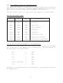
Table 4.3-1: The Baud Rate Selection Jumper B7
PIN
Connection
between
#10 and #11
No Connection
between
#10 and #11
1,3,5
9600 Baud
38400 Baud
2,4,6
4800 Baud
19200 Baud
15,17,19
2400 Baud
9600 Baud
7
1200 Baud
4800 Baud
14
600 Baud
2400 Baud
8
300 Baud
1200 Baud
13
150 Baud
600 Baud
9
110 Baud
440 Baud
12
60 Baud
240 Baud
The baud rates of the terminal, host and remote interface are, in
default during manufacturing, connected to 9600 Baud.
4-17
Figures 4.3-1 and 4.3-3 show the detailed hardware drawing and the
jumper location diagram.
4-18
Figure 4.3-1:
Hardware Drawing of the Baud Rate Selection Parts
4-19
Figure 4.3-2:
Default Jumper Settings of B7
10 - 11;
1 - 20;
3 - 18;
5 - 16
11
o
o
10
12
o
o
9
13
o
o
8
14
o
o
7
15
o
o
6
16
o
o
5
17
o
o
4
18
o
o
3
19
o
o
2
20
o
o
1
4-20
Figure 4.3-3:
Location Diagram of the Baud Rate Selection Parts
4-21
4.3.2
Timing of the ACIAs
The ACIA is a controller device of the synchronous 6800 family.
Therefore, the access cycle is controlled by the processor signals
VMA*, VPA*, and the E signal.
To initiate the transfer, the processor must receive the VPA*
signal from the decoding logic. When the CPU is synchronized to
the E clock signal, the VMA* signal is asserted to signal the I/O
devices that the transfer is beginning.
The synchronization
requires additional time (1000ns maximum).
The timing diagrams illustrating the best and worst cases are shown
in Figures 4.3-4 and 4.3-5.
Tables 4.3-2 and 4.3-3 list the related values.
Table 4.3-2: ACIA Timing (best case)
No
Description
Min
1
AS* low
2
AS* asserted to VPA*
asserted
AS* inactive to VPA*
inactive
VMA* asserted (8MHz Processor
clock frequency)
VMA* asserted (12.5MHz
Processor clock frequency)
VPA* to VMA* delay
3
4a
4b
5
Max
800
Unit
ns
30
80
ns
30
80
ns
850
1000
ns
600
750
ns
-
150
Min
Max
Unit
-
2000
ns
30
80
ns
30
80
ns
850
1000
ns
600
750
ns
-
1000
ns
Table 4.3-3: ACIA Timing (worst case)
No
Description
1
AS* low
2
AS* asserted to VPA*
asserted
AS* inactive to VPA*
inactive
VMA* asserted (8MHz Processor
clock frequency)
VMA* asserted (12.5MHz
Processor clock frequency)
VPA* to VMA* delay
3
4a
4b
5
4-22
Figure 4.3-4:
ACIA Timing Diagram (best case)
4-23
Figure 4.3-5:
ACIA Timing Diagram (worst case)
4-24
4.3.3
The Terminal Port
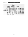
The RS232 (C) interface is used to communicate via Port 1
(connector P4) with a standard terminal. The transmission format
is initially preset as follows:
8 data bits
1 stop bit
No parity
Asynchronous protocol
The terminal must be set to these conditions.
The terminal interface can interrupt the 68000 CPU on level 4. The
forced interrupt vector is the auto interrupt vector (#28/$000070).
4.3.3.1
The I/O Signal Assignment
Further details of control functions and port format changes are
shown in the software manual of the used system monitor.
The
detailed hardware diagram of the interface is given in Figure
4.3-6.
The default signal assignments during manufacturing are listed in
Table 4.3-4.
4-25
Figure 4.3-6:
Hardware Diagram of the Terminal Port
4-26
Table 4.3-4:
P4 PIN
Terminal Connector Signal Assignments
INPUT
OUTPUT
SIGNAL
1
2
X
3
Receive Data (RXD)
X
Transmit Data (TXD)
X
Request to Send (RTS)
4
5
6
7
Signal GND
8
X
9
Data Carrier Detect (DCD)
Signal GND
19
20
X
Clear to Send (CTS)
The location diagram of the terminal interface parts is shown in
Figure 4.3-7.
4-27
This page was intentionally left blank
Table 4.3-5:
Default Jumper Setting at B3
2-19;
3-18;
4-17;
5-16;
7--8;
10-11;
6-13;
11
o
o
10
12
o
o
9
13
o
o
8
14
o
o
7
15
o
o
6
16
o
o
5
17
o
o
4
18
o
o
3
19
o
o
2
20
o
o
1
4-29
Figure 4.3-7:
Location Diagram of the Terminal Port
4-30
4.3.3.2
Register Layout
Device:
6850
ACIA
(Terminal)
Address
Mode
Description
0C0080
R
Status Register
0C0080
W
Control Register
0C0082
R
Receive Data Register
0C0082
W
Transmit Data Register
4.3.3.3
Baud Rate Selection
Please see chapter 4.3.1 "The Baud Rate Selection".
4.3.3.4
Terminal Port Summary
Start Address
End Address
$0C0080
$0C0082
Access Mode
Byte Only
Read and Write
Usable Data Bits
D8-D15
Access Time
1000ns (min)
2000ns (max)
Interrupt Request Level
4
Interrupt Handling
fixed IRQ vector (#28)
Address:$000070
4-31
4.3.4
The Remote Port
The second RS232 compatible interface is the Remote Interface.
The hardware drawing is shown in Figure 4.3-8 and the location
diagram of the interface parts is outlined in Figure 4.3-9.
The Remote Interface can interrupt the 68000 CPU on level 3.
forced interrupt vector is the autovector (#27/$000006C).
4.3.4.1
The
The I/O Signal Assignment
Further details of control functions and port format changes are
shown in the software manual of the system monitor used.
The
detailed hardware diagram of the interface is outlined in Figure
4.3-8.
The signal assignments are listed in Table 4.3-6 and the default
signal assignments during manufacturing are listed in Table 4.3-7.
4-32
Figure 4.3-8:
Hardware Diagram of the Remote Port
4-33
Figure 4.3-9: Location Diagram of the Remote Port
4-34
Table 4.3-6:
P5 PIN
Remote Connector Signal Assignments
INPUT
OUTPUT
SIGNAL
1
2
X
3
Receive Data (RXD)
X
Transmit Data (TXD)
X
Request to Send (RTS)
4
5
6
7
Signal GND
8
X
9
Data Carrier Detect (DCD)
Signal GND
19
20
X
Clear to Send (CTS)
4-35
Table 4.3-7: Default Jumper Settings at B1
PIN 2-19;
3-18;
4-17;
5-16;
7-8;
10-11;
6-13;
11
o
o
10
12
o
o
9
13
o
o
8
14
o
o
7
15
o
o
6
16
o
o
5
17
o
o
4
18
o
o
3
19
o
o
2
20
o
o
1
4-36
4.3.4.2
Register Layout
Device:
6850
ACIA
(Remote)
Address
Mode
Description
0C0101
R
Status Register
0C0101
W
Control Register
0C0103
R
Receive Data Register
0C0103
W
Transmit Data Register
4.3.4.3
Baud Rate Selection
Please see Chapter 4.3.1
"The Baud Rate Selection".
4-37
4.3.4.4
Remote Port Summary
Start Address
End Address
$0C0101
$0C0103
Access Mode
Byte Only
Read and Write
Usable Data Bits
D0-D7
Access Time
1000ns (min)
2000ns (max)
Interrupt Request Level
3
Interrupt Handling
fixed IRQ vector (#27)
Address:$00006C
4-38
4.3.5
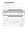
The Host Port
The third on-board RS232(C) interface can be used in conjunction
with a host computer. The detailed schematic is given in Figure
4.3-10.
A standard communication method to communicate between a terminal
(connector P4) and a host computer (connector P3) is the
Transparent Mode.
When the Transparent Mode is used, all
transmitted characters are sent directly from the terminal to the
host computer and no correction or modification is carried out by
the SYS68K/CPU-6 board. In a configuration like the one shown in
Figure 4.3-11, both computers are configured to receive data on the
Transmit Data Line (TXD) from the terminal and echo it via the
Receive Data Line (RXD) back to the terminal. The SYS68K/CPU-6
board polls the terminal ACIA registers in the Transparent Mode.
When the user types in the valid stop character sequence, the CPU
recognizes it, stops the transmission of the following characters
from the terminal to the host computer, and returns to the system
monitor program. The stop character sequence is the last character
sequence that the SYS68K/CPU-6 board sends to the host computer.
If the connected device cannot drive the CTS signal to high state,
a connection from P3 pin 5 to pin 20 has to be hardwired.
The baud rate of each module (terminal, SYS68K/CPU-6 board terminal
interface, and host computer interface) must be jumpered equally.
The baud rate of the host ACIA remains unaltered because the
Transparent Mode handling does not use this ACIA for the transfer.
A detailed description of the data format and the system monitor
Dump/Load (DU/LO) commands is given in the Software User’s Manual.
The Host Interface can interrupt the 68000 CPU on level 2. The
forced interrupt vector is the autointerrupt vector (#26/$000068).
4-39
Figure 4.3-10: Configuration with a Host Computer
4-40
Figure 4.3-11: Interfacing to a Host Computer in the Transparent
Mode
4-41
4.3.5.1
The I/O Signal Assignment
Further details of control functions and port format changes are
shown in the VMEPROM user’s manual of the system monitor used.
The detailed hardware diagram of the interface is shown in Figure
4.3-12.
The signal assignments are outlined in Table 4.3-8.
The default signal assignments during manufacturing are listed in
Table 4.3-9.
4-42
Table 4.3-8: Host Signal Assignments
P3 PIN
INPUT
OUTPUT
1
SIGNAL
Protective GND
2
X
Transmit Data (TXD)
3
X
Receive Data (RXD)
5
X
Clear to Send (CTS)
7
X
X
Signal GND
9
X
X
Signal GND
X
Clear to Send (CTS)
18
20
4-43
Figure 4.3-12: Hardware Diagram of the Host Port
4-44
Table 4.3-9: Default Jumper Settings at B5
PIN 2-15;
3-14;
4-13;
5-12;
7-10;
8-9;
9
o
o
8
10
o
o
7
11
o
o
6
12
o
o
5
13
o
o
4
14
o
o
3
15
o
o
2
16
o
o
1
4-45
Figure 4.3-13: Location Diagram of the Host Port
4-46
4.3.5.2
Register Layout
Device:
6850
ACIA
(Host)
Address
Mode
Description
0C0041
R
Status Register
0C0041
W
Control Register
0C0043
R
Receive Data Register
0C0043
W
Transmit Data Register
4.3.5.3
Baud Rate Selection
Please see Chapter 4.3.1
4.3.5.4
"The Baud Rate Selection".
Host Port Summary
Start Address
End Address
$0C0041
$0C0043
Access Mode
Odd Byte Only
Read and Write
Usable Data Bits
D0-D7
Access Time
1000ns (min)
2000ns (max)
Interrupt Request Level
2
Interrupt Handling
fixed IRQ vector (#26)
Address:$000068
4-47
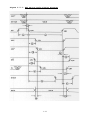
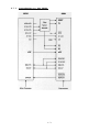
4.4
The Parallel Interface and Timer Chip
The Parallel Interface and Timer module (PI/T 68230) is used on the
board to provide powerful asynchronous parallel I/O on the
SYS68K/CPU-6 board.
Easy access to the PI/T is provided by the asynchronous bus
structure and the nonmultiplexed data/address bus. This allows
effective communication to the PI/T.
Features of the PI/T 68230
-
Port Modes include:
- Bit I/O
- Unidirectional 8 Bit and 16 Bit
- Bidirectional 8 Bit and 16 Bit
-
Selectable Handshaking Options
-
24 Bit Programmable Timer with 5 Bit Prescaler
-
Software Programmable Timer Modes
-
2 Selectable Interrupt Sources
-
Registers are readable and writeable
-
All registers are directly addressable
The detailed hardware connection of the PI/T is outlined in Figure
4.4-1.
4-48
Figure 4.4-1: The Hardware Diagram of the PI/T
4-49
4.4.1
The PI/T Register Layout and Addressing
All of the PI/T registers are directly
read/writeable as shown in Table 4.4-1.
addressable
and
The base address is $0E0000. Only single byte transfers to/from
the PI/T on the data bits D0-D7 are allowed (odd addresses).
The absolute access address of the first register under the default
conditions during manufacturing is $0E0001.
Caution:
The Interrupt Vector Number Registers PIVR (address
$0E000B) and TVIR (address $0E0023) are programmable,
but no interrupt vector can be forced because of the
auto interrupt vectoring.
The PI/T is used as an internal control device for steering and
controlling of the local functions.
4.4.2
The Timer
The TIMER INTERRUPT function is performed by the timer module of
the PI/T device. This independent part of the PI/T contains a 24
bit wide counter and a 5 bit prescaler.
The timer may generate periodic interrupts or a single interrupt
after a programmable time period. It may be used as a watchdog
timer or for elapsed time measurements. The timer is clocked by
the 8 MHz frequency of the PI/T clock input.
4-50
Table 4.4-1: The PI/T Address Map
Base Address : $0E0000
Offset
Reset
Value
Label
Description
01
00
PITPGCR
Port General Control Register
03
00
PITPSRR
Port Service Request Register
05
00
PITPADDR
Port A Data Direction Register
07
00
PITPBDDR
Port B Data Direction Register
09
00
PITPCDDR
Port C Data Direction Register
0B
0F
PITPIVR
Port Interrupt Vector Register
0D
00
PITPACR
Port A Control Register
0F
00
PITPBCR
Port B Control Register
11
--
PITPADR
Port A Data Register
13
--
PITPBDR
Port B Data Register
15
--
PITPAAR
Port A Alternate Register
17
--
PITPBAR
Port B Alternate Register
19
--
PITPCDR
Port C Data Register
1B
--
PITPSR
Port Status Register
21
00
PITTCR
Timer Control Register
23
0F
PITTIVR
Timer Interrupt Vector Reg.
25
27
29
2B
-----
PITCPR
Counter Preload Register
2D
2F
31
33
-----
PITCNTR
Count Register
35
00
PITTSR
Timer Status Register
4-51
This page was intentionally left blank
Table 4.4-2: Default Jumper Settings for B24 and B24A
B24: 1
3
4
7
10
13
16
19
B24A:
-
2
6
5
8
11
14
17
20
B24
21
o
o
o
19
21
o
o
o
19
18
o
o
o
16
18
o
o
o
16
15
o
o
o
13
15
o
o
o
13
12
o
o
o
10
12
o
o
o
10
9
o
o
o
7
9
o
o
o
7
6
o
o
o
4
6
o
o
o
4
o
o
o
o
o
o
3
2
1
3
2
1
1 - 6
2 - 5
3 - 4
B24A
4
o
o
3
4
o
o
3
5
o
o
2
5
o
o
2
6
o
o
1
6
o
o
1
4-53
Figure 4.4-2:
The Location Diagram of the PI/T and the Jumperfields
4-54
4.4.3
Interrupt Handling
The PI/T is able to force an interrupt to the CPU. This function
allows the use of the included timer as a time base for
multitasking software.
Figure 4.4-2 outlines the location diagram of the PI/T and the
interrupt request jumper field.
The general purpose 24 bit timer with its 5 bit prescaler can be
used as an output for programmable frequencies with internal or
external clocks, as a watchdog and as a normal time base. The
interrupt request level of both interrupt signal lines is level 5.
The interrupt autovectoring is used on the board. Therefore, the
fixed interrupt vector number for the PI/T is #29.
The address $000074 contains the start address of the PI/T
interrupt handling routine. Please refer to the PI/T 68230 data
sheet; it includes all the programming details that are important
for the PI/T handling.
4.4.4
Summary of the PI/T
Access Address
:
$0E0001 - $0E0035
Access Mode
:
Odd Byte Only
Read and Write transfer
Usable Data Bits
:
D0 - D7
Interrupt Level
:
5 (auto interrupt vectoring)
Interrupt Vector
:
Fixed: #29
Address: $000074
4-55
4.5
The Real Time Clock
The on-board Real Time Clock (RTC 58167A) can be used as a
calendar, a real time counter and for time measurements.
Features of the Real Time Clock
-
1/10000 of a second through month counter
-
56 bits of RAM with comparator to compare the real time
counter to the RAM data.
-
Interrupt Output with 8 possible interrupt signals
-
Power Down
signals
-
Status register to indicate rollover during a read cycle
-
32,768 Hz crystal oscillator
-
Four year calendar (no leap year)
-
24 hour clock
-
Battery backup during main power down
mechanism
disables
4-56
all
input
and
output
4.5.1
Register Layout
The access address of the RTC register is $0C0401 to $0C042F. Only
single byte transfers to and from the RTC on the data bits D0-D7
are allowed. All of the RTC registers are directly addressable and
read/writeable as shown in Table 4.4-1
4.5.2
Access Timing
The read/write timing diagram and the time values are given in
Figures 4.5-1 and 4.5-2 and in Tables 4.5-2 and 4.5-3.
The RTC is a metal gate CMOS circuit which has an access time of
approximately 1100ns. This requires a special delay of the DTACK*
signal to the CPU by an access to/from the RTC.
4.5.3
The Battery Backup Mode
A lithium battery is included in the shipment. This battery is not
soldered onto the board because of the use of aluminium foil for
packing during shipping.
The location diagram of the position of the battery is outlined in
Figure 4.5-3.
4-57
Table 4.5-1: Register Model of the RTC
Default Board Base Address: $0C0401
Default Register Reset
Address Offset Value
HEX
Label
Description
0C0401
01
--
RTCCTTS
Counter - ten thousands of secs
0C0403
03
--
RTCCHTS
0C0405
05
--
RTCCSEC
Counter - hundredths + tenths of
secs
Counter - seconds
0C0407
07
--
RTCCMIN
Counter - minutes
0C0409
09
--
RTCCHRS
Counter - hours
0C040B
0B
--
RTCCDOW
Counter - day of week
0C040D
0D
--
RTCCDOM
Counter - day of month
0C040F
0F
--
RTCCMON
Counter - month
0C0411
11
--
RTCRTTS
RAM - ten thousandths of secs
0C0413
13
--
RTCRHTS
RAM - hundredths + tenths of secs
0C0415
15
--
RTCRSEC
RAM - seconds
0C0417
17
--
RTCRMIN
RAM - minutes
0C0419
19
--
RTCRHRS
RAM - hours
0C041B
1B
--
RTCRDOW
RAM - day of week
0C041D
1D
--
RTCRDOM
RAM - day of month
0C041F
1F
--
RTCRMON
RAM - month
0C0421
21
--
RTCISR
Interrupt Status Register
0C0423
23
--
RTCICR
Interrupt Control Register
0C0425
25
--
RTCCRES
Counters reset
0C0427
27
--
RTCRRES
RAM reset
0C0429
29
--
RTCSTAT
Status bit
0C042B
2B
--
RTCGO
GO command
0C042D
2D
--
RTCSINT
Standby interrupt
0C042F
2F
--
RTCTEST
Test mode
4-58
Table 4.5-2: RTC Write Time Values
Number
(Note A)
Min. Max.
Parameter
1
Axx valid and IACK* high to AS* low
10
3
AS* high
30
4
AS* low to CSRTC active
0
5
AS* active
0
6
AS* invalid to UDS* high
0
40
7
AS* inactive to CSRTC inactive
0
40
8
AS* low to LDS* low (WRITE)
10
130
9
AS* low to DTACK* low
1000
2000
11
AS* inactive to DTACK inactive
15
45
12
AS* active to WRITE* low
10
150
13
AS* inactive to WRITE* inactive
10
70
14
Data valid to Data Strobes active
10
15
As* inactive to Data invalid
10
4-59
45
Figure 4.5-1: RTC Write Cycle Timing Diagram
4-60
Table 4.5-3: RTC Read Time Values
Number
(Note A)
Min. Max.
Parameter
1
Axx valid and IACK* high to AS* low
10
3
AS* high
30
4
AS* active to CSRTC low
30
60
5
AS* low
1800
2500
6
AS* inactive to UDS* inactive
10
60
7
AS* inactive to CSRTC inactive
0
40
8
AS* active to LDS* valid
10
130
9
AS* low to DTACK low
1800
2500
45
11
AS* inactive to DTACK inactive
15
12
WRITE* high to AS* active
10
14
Data valid to DTACK active
10
15
DTACK inactive to Data invalid
10
4-61
60
Figure 4.5-2: RTC Read Cycle Timing Diagram
4-62
4.5.4
The Interrupt Assignment
The RTC can be used to force an interrupt to the on-board CPU.
This is provided if a jumper is inserted in the jumperfield B200.
Otherwise, no interrupt can be forced and the interrupt request
line is always disabled. The RTC interrupt request level is fixed
at level 6, the highest maskable interrupt level.
The jumper location diagram of the RTC circuit is shown in Figure
4.5-3.
The interrupt control logic on the board decodes the RTC Interrupt
Request level (IRQ6) and forces the autointerrupt vector after the
interrupt has been acknowledged on that level.
This vector is
fixed and reserved on the board specially for the RTC. The long
word stored at address $000078 (vector no. 30) represents the RTC
interrupt handling routine start address.
4.5.5
Summary of the RTC
Access Address
:
$0C0401 - $0C042F
Access Mode
:
Odd Byte Only
Read and Write cycles
Usable Data Bits
:
D0 - D7
Interrupt Level
:
6 (auto interrupt vectoring)
Interrupt Vector
:
Fixed: #30
Address: $000078
4-63
Figure 4.5-3: The Location Diagram of the RTC
4-64
4.6
The Dynamic RAM
The on-board RAM area is used for the CPU’s exception vector table,
as scratch pad for the system monitor, called SYS68K/CPU-6, and for
the user program/data. The dynamic RAM area consists of 512 Kbytes
on the SYS68K/CPU-6.
The DRAM has an access time of 150ns (typical) if no refresh cycle
is under execution.
4.6.1
Address Map and Capacity
Address
000 000
:
000 007
ROM Initialization Vectors from System EPROM
000 008
:
007 FFF
SYSTEM DRAM Area Reserved
008 000
:
07F FFF
USER DRAM Area 512 Kbytes
4.6.2
Access Timing of the DRAM
This paragraph describes all of the timings to/from the DRAMs.
In general, the DRAMs are 120ns devices which operate at an
effective access time of 150ns.
A fully asynchronous control logic drives the access cycles as well
as the refresh cycles.
The refresh circuitry generates one refresh cycle every 15
microseconds. Therefore, the board can be used to operate in high
end real time applications.
The detailed timing diagram is shown in Table 4.6-1 and Figure
4.6-1.
4-65
Table 4.6-1:
Time Values for an Access Cycle without Refresh
Request
(ns)
Min.
(ns)
Max.
1. AS* active to Access Request
active
10
33
2. AS* active to Access Cycle
start
33
66
3. AS* active to DTACKOUT*
asserted
285
328
4. AS* active to AS*
inactive
285
14000
5. AS* inactive to DTACKOUT*
inactive
30
45
6. AS* inactive to Access Cycle
inactive
15
25
7. Data valid before DTACK*
asserted
10
-
SIGNAL DESCRIPTION
4-66
Figure 4.6-1: Access Cycle without Refresh Request
4-67
4.6.3
Refreshing of the DRAMs
The Dynamic RAM refresh is accomplished by performing a memory
cycle at each of the 128 row addresses at an interval of 2ms. The
"RAS Only Refresh" results in a substantial reduction of operating
power. For real time operations, the refresh is fully asynchronous
to the LOCAL and VMEbus accesses.
A maximum delay of 300ns for an access is required, when a refresh
request is pending at the same time as an access request, because
the refresh has the highest priority.
The refresh is organized in 128 steps every 2ms. This requires a
minimum time delay, if access requests are pending and refresh is
in process.
The repetition rate for a refresh cycle is 15
microseconds.
The detailed timing diagram of the refresh is shown in Figure
4.6-2.
4-68
Figure 4.6-2: The Global Refresh Timing Diagram
4-69
4.6.4
The Summary of the DRAM
Start Address
$000008
End Address
$07FFFF
Boundary
$080000
Access Modes
Byte or Word
(512K bytes)
Read or Write
Usable Data Bits
D0-D7 and D8-D15
Access Time
150ns (min)
165ns (typ)
520ns (max) with Refresh
4-70
4.7
The Floating Point Coprocessor 68881 (FPCP)
The 68881 FPCP is designed to operate as a coprocessor with the
68020 microprocessor or as a peripheral device with the 68000/68010
microprocessors.
There is a software handshake defined for
intercommunication between the CPU and the FPCP. This procedure
is performed by the 68020 on its own, while 680x0 microprocessors
need a software package to run the handshake. The procedure is
described in the 68020 User’s Manual (the 68020 coprocessor
interface handshake protocol). The specific application of the
protocol is described in the 68881 User’s Manual.
The offset of the FPCP to the I/O Area Base Address is $200, so the
base address of the FPCP is $0E0200.
The 68881 data sheet is included in Appendix H.
The 68881 Floating Point Coprocessor operating at 12.5 MHz clock
frequency is a full implementation of the IEEE Standard P754 for
Floating Point Arithmetic (Draft 10.0)
A set of eight general Floating Point Data Registers, supporting
full 80 bit extended precision are available for arithmetic
operations such as:
Add
Subtract
Multiply
Divide
Compare
Scale Exponent
Modulo
Conditional Branches
Absolute Value
Sin, cosine, hyperbolic sin and cosine
Tangent, cotangent, hyperbolic tangent and cotangent
e EXP(x)
e EXP(x-1)
E EXP(xtract(4))
ln(x), ln(x+1)
log 10(x), log 2(x)
2 EXP(x), 10 EXP(x)
Square root
Conditional Trap (32)
The FPCP supports the following data types:
Word and Long Integers
Single, Double and Extended Precision Real Numbers
Packed BCD String Real Numbers
4-71
4.7.1
Interfacing to the 68881
4-72
4.7.2
The Data Format of the 68881
The 68881 contains seven data types supported by all arithmetic and
transcendal operations.
Example:
FADD.B
FADD.W
FADD.L
FADD.S
FADD.D
FADD.X
FADD.P
#0,FP0
D2,FP3
BIGINT,FP7
#3.14159,FP5
(SP)+,FP6
Byte Integer (B)
Word Integer (W)
Long Word Integer (L)
Single Precision Real (S)
Double Precision Real (D)
[(TEMP_PTR,A7)],FP3
#1.23E25,FP0
Extended Precision Real(X)
Packed Decimal Real (P)
Figure 4.7-1 outlines the data format summary of the 68881 and
Figure 4.7-2 shows the register layout of the internal register of
the 68881.
Please refer to the 68881 User’s Manual for further details.
4-73
Figure 4.7-1:
Data Format Summary of the 68881
4-74
Figure 4.7-2:
79
Register Model of the 68881
63
0
FP0
FP1
FP2
FP3 Floating Point
FP4 Data Registers
FP5
FP6
FP7
31
23
15
7
0
....................
:
0
Exception Mode
FPCR
:................... Enable
Control
Condition
Code
Quotient Exception Accrued
Status Exception
FPSR
Control Register
Status Register
FPIAR Instruction
Address Register
4-75
4.7.3
The 68881 Instruction Set
The 68881 instruction set is organized into six major classes:
1)
2)
3)
4)
5)
6)
Moves between the 68881 (in and out),
Move multiple registers (in and out),
Monadic operations,
Dyadic operations,
Branch, set, or trap conditionally, and
Miscellaneous.
4.7.4
Addressing of the 68881
The 68881 is addressed via a part of the address signals.
The coprocessor address is $0E02XX.
The Coprocessor Interface Register Map
31
15
0
00
RESPONSE
CONTROL
04
SAVE
RESTORE
08
OPERATION
COMMAND
0C
(RESERVED)
CONDITION
10
14
OPERAND
REGISTER SELECT
(RESERVED)
18
INSTRUCTION ADDRESS
1C
OPERAND ADDRESS
4-76
4.7.5
Detection of the 68881
The sense pin of the FPCP is not connected.
Should an address of a nonpresent FPCP be addressed ($0E02XX) then
a bus error will occur.
4.7.6
RESET of the FPCP
The FPCP can be RESET by executing the following small program:
FPCP: MOVE.W
MOVE.W
LOOP: SUBQ.W
BNE.S
MOVE.W
END
#$100,D0
#$0,$0E0380
#$1,D0
LOOP
#$0,$0E0300
INIT RESET
TURN RESET OFF
The RESET instruction of the 68000/68010 does not reset the FPCP
in a proper way so that the software RESET has to be used. The
RESET has to be activated for at least 100us.
4.7.7
Summary of the 68881
Coprocessor address
$0E0200
Usable Data Bits
D0 - D15
Supported Transfer Types
Byte
Word
Reset Function
Reset on:
write word to $0E0380
(min 100us)
Reset off: write word to $0E0300
4-77
4.8
Local Interrupt Handling
The on-board CPU is able to handle seven different prioritized
interrupt request levels. The interrupt daisy chain on the VMEbus
allows an unlimited number of peripheral devices to interrupt the
CPU.
Interrupt priority levels are numbered from one to seven, level
seven being the highest priority. The status register contains a
three bit mask which indicates the current priority of the
processor. Interrupts for all priority levels less than or equal
to the current processor priority are ignored.
Interrupt requests arriving at the processor do not force immediate
exception processing.
Pending interrupts are detected between
instruction executions. If the priority of the pending interrupt
request is lower than or equal to the current processor priority,
the execution continues with the next instruction and no interrupt
exception processing is started.
If the priority of the pending interrupt is greater than the
current processor priority, then the exception processing sequence
is started.
After the start of the interrupt exception sequence, a copy of the
Status Register (SR) is saved on the stack, the privilege state of
the processor is set to supervisor, and the processor priority
level is set to the level of the interrupt being acknowledged.
The processor fetches the vector number from the interrupting
device, classifying the reference as an interrupt acknowledge and
displaying the level number of the interrupt being acknowledged on
the address bus using the address signals A1, A2 and A3 as listed
in Table 4.8-1.
Table 4.8-2 shows the conversion of the interrupt vector into the
address under which the start address of the interrupt service
routine is stored.
4-78
Table 4.8-1: The Interrupt Acknowledge Level Code
IRQ
Level
A3
A2
A1
FC0
FC1
FC2
7
1
1
1
1
1
1
6
1
1
0
1
1
1
5
1
0
1
1
1
1
4
1
0
0
1
1
1
3
0
1
1
1
1
1
2
0
1
0
1
1
1
1
0
0
1
1
1
1
-
0
0
0
1
1
1
Note A)
Note
A
Not assigned.
The content of the interrupt vector whose vector number was fetched
and translated is loaded into the program counter to start the
interrupt handling routine.
The vector that was moved from the interrupting device onto the
data bits D0-D7 is translated by the CPU into an address which
contains the start address of the interrupt handling routine.
Table 4.8-2: The Interrupt Vector Conversion
D16
D8
D7
ignored
A16
D0
V7........V2 V1 V0
A8
A7
0 0 0 0 0 V7 V6
A1 A0
V5........V0 V0 V0
4-79
Peripheral
Vector
Number
Translated
Address
from the 8
bit vector
number
4.8.1
Interrupt Level Assignment
The SYS68K/CPU-6 board contains six on-board interrupt sources, the
three serial I/O Controllers (ACIAs), the ABORT function switch,
the Parallel Interface and the Real Time Clock.
Table 4.8-1 lists the combinations of the on-board devices and the
corresponding interrupt level as well as the default set autointerrupt vectors.
Table 4.8-3: The On-Board Devices Interrupt Scheme
Interrupt
Level
Autointerrupt
Vectoring
ABORT Switch
7
YES
31
$00007C
RTC 58167A
6
YES
30
$000078
PI/T 68230
5
YES
29
$000074
ACIA Terminal
4
YES
28
$000070
ACIA Remote
3
YES
27
$00006C
ACIA Host
2
YES
26
$000068
ACFAIL, SYSFAIL
5 a)
YES
29
$000074
On-Board Device
Note:
Default
Vector
Address
On request, this signal from the VMEbus can be used to
generate an Interrupt. (Please refer to Chapter 5.7.2)
4-80
4.8.2
Usage of the Auto Vectors
Table 4.8-4 lists the vector numbers for the autointerrupt scheme
and the spurious interrupt.
Table 4.8-4: The Autointerrupt Vector Table
Absolute
Address
Vector
Number
Corresponding
Interrupt Level
$000060
# 24
Spurious Interrupt
$000064
# 25
Level 1 Interrupt Autovector
$000068
# 26
"
2
"
"
$00006C
# 27
"
3
"
"
$000070
# 28
"
4
"
"
$000074
# 29
"
5
"
"
$000078
# 30
"
6
"
"
$00007C
# 31
"
7
"
"
A global timing diagram of the interrupt vector acquisition is
shown in Figure 4.8-1.
The priority level seven is a special case. Level seven interrupts
cannot be disabled by the interrupt priority mask. The IRQ 7 is
a "non-maskable interrupt"
4-81
Figure 4.8-1: The Global Interrupt Vector Acquisition
4-82
4.8.3
Summary of the Local Interrupts
Device
Type
IRQ Level
IRQ Vector
Address
--
7
31
$00007C
58167A
RTC
6
30
$000078
68230
PI/T
5
29
$000074
68B50
ACIA
Terminal
5
28
$000070
68B50
ACIA
Remote
3
27
$00006C
68B50
ACIA
Host
2
26
$000068
ABORT Switch
4-83
4.9
The BERR Generator
To provide an error function, if a device or memory on the bus has
not responded within a maximum time, a time-out counter is used on
the board.
This time-out counter generates a Bus Error Signal (BERR*) after
a user-supplied time limit (up to 15ms).
The CPU aborts the
current cycle if the BERR* signal has been recognized, and forces
the exception routine.
Figure 4.8-1 shows the detailed diagram of an access cycle aborted
via BERR* with the default set values.
Table 4.9-1 lists the usable time-out values and the equivalent
jumper settings. Figure 4.9-2 outlines the location diagram of the
jumperfields.
If the board is the current VMEbus master, and an external VMEbus
card generates a BERR*, then the cycle will be aborted in the same
way.
For example, an external BERR* signal can be generated by a dynamic
memory card by using an Error Detection and Correction Logic (EDC)
and detection of a non-correctable data pattern.
4-84
Figure 4.9-1:
Timing Diagram of a BERR Cycle
4-85
Table 4.9-1: BERR Jumper Settings A
B33
B34
o
3
o
o
o
o
o
13
2
o
o
o
10
1
o
o
o
7
o
o
o
4
o
o
o
1
o
3
o
2
o
1
Time Out
Min
Max
B25
24ms
32ms
Default setting during manufacturing
Table 4.9-2: BERR Jumper Settings B
B33
B34
Time Out
o
3
o
o
o
o
o
13
2
o
o
o
10
1
o
o
o
7
o
o
o
4
o
o
o
1
o
3
o
2
o
1
Min
Max
B25
8ms
16ms
4-86
Table 4.9-3:
B33
B34
BERR Jumper Settings C
o
3
o
o
o
o
o
13
2
o
o
o
10
1
o
o
o
7
o
o
o
4
o
o
o
1
o
o
13
o
3
o
2
o
1
Time Out
Min
Max
B25
2.5ms
3.0ms
Table 4.9-4: BERR Jumper Settings D
B33
o
3
B25
o
\
B34
Time Out
o
2
o
o
o
10
o
1
o
o
o
7
o
o
o
4
o
o
o
1
o
3
o
2
o
1
Min
Max
224ms
256ms
4-87
Figure 4.9-2: Location Diagram of the BERR Jumperfield
4-88
This page was intentionally left blank
5.0
THE VMEbus INTERFACE
The SYS68K/CPU-6 board contains a VMEbus interface which allows the
following transfer modes:
A24 : D16, D8
A16 : D16, D8
The standard
controlled via
the A23 mode.
of the address
addressing (A24) and the short I/O (A16) are
hardware because the A16 mode is only a subset of
The address range of the short I/O is the upper end
range of the 68000/68010.
Short I/O address range : $FF0000 to $FFFFFF
All address modifier signals, as well as the interrupt request
lines are supported by the SYS68K/CPU-6.
5.1
Data Transfer Size
If this board is the current VMEbus master (low driven BBSY*
signal) and the current access address is higher or equal to
$100.000, then a VMEbus transfer is initiated. Figures 5.1-1 and
5.1-2 show the detailed timing diagrams of a read cycle and a write
cycle. Tables 5.1-1 and 5.1-2 list all of the time values.
5-1
Table 5.1-1:
NUMBER
1
Read Cycle followed by Write Cycle
NOTE
MIN. MAX.
PARAMETER
NOTES
3
Axx and AMx valid and IACK* high
to AS* low
DTACK* low to invalid address or
IACK* low
AS* high
4
DTACK* low to AS* high
0
C
5
AS* to DS"A"* skew
0
B
6
WRITE* valid to DS"A"* low
35
B
7
DS"B"* high to invalid WRITE*
10
B
8
DTACK* high to active data bus
0
C
9
Dxx valid to DS"A"* low
35
B
C
2
35
B
0
C
40
B
10
DTACK* low to invalid data
0
11
DS"A"* to DS"B"* skew
0
12
DTACK*/BERR* low to DS"A"* high
0
C
13
DS"A"* high
40
B
14
DS"B"* high to DS"A"* low
40
B
15
DS"B"* high
40
B
16
DS"B"* high to DTACK* high
0
D
17
DTACK*/BERR* low to DS"B"* high
0
C
18
DS"A" low to DTACK* or BERR
asserted
0
E
10
B
A.
All times given in nanoseconds.
B.
The MASTER must guarantee this timing between two of its
outgoing signal transitions.
C.
The MASTER must wait for the incoming signal edge from the
SLAVE before changing the level of its outgoing signal.
D.
This is a guarantee that the SLAVE will not change the
incoming signal until the SLAVE changes its outgoing signal.
E.
The MASTER is guaranteed this timing between two of its
incoming signal transitions.
5-2
Figure
5.1-1:
Read Cycle Followed by Write Cycle
5-3
Table 5.1-2:
NUMBER
1
Write Cycle followed by Read Cycle
NOTE
MIN. MAX.
PARAMETER
NOTES
3
Axx and AMx valid and IACK* high
to AS* low
DTACK* low to invalid address or
IACK* low
AS* high
4
DTACK* low to AS* high
0
C
5
AS* to DS"A"* skew
0
B
6
WRITE* valid to DS"A"* low
35
B
7
DS"B"* high to invalid WRITE*
10
B
8
Data release to DS"A" low
0
B
9
DS"A"* to DS"B" skew
2
10
DTACK* low to DS"A"* high
11
35
B
0
C
40
B
10
B
0
C
DS"A"* high
40
B
12
DS"B"* high to DS"A" low
40
B
13
DTACK*/BERR* high to DS"A"* low
0
C
14
DTACK* low to DS"B"* high
0
C
15
DS"A"* high to invalid data
0
D
16
DS"B"* high
40
B
17
Dxx valid to DTACK* low
-25
E
18
Data released to DTACK*/BERR*
high
DS"B"* high to DTACK*/BERR* high
0
E
30
B
19
NOTES:
A.
B.
C.
D.
E.
All times given in nanoseconds.
The MASTER must guarantee this timing between two of its
outgoing signal transitions.
The MASTER must wait for the incoming signal edge from the
SLAVE before changing the level of its outgoing signal.
This is a guarantee that the SLAVE will not change the
incoming signal until the MASTER changes its outgoing signal.
The MASTER is guaranteed this timing between two of its
incomingsignal transitions.
5-4
Figure 5.1-2:
Write Cycle Followed by Read Cycle
5-5
This page was intentionally left blank
5.2
The Address Modifier Implementation
The 68000 CPU contains three function code signals which indicate
the state of the processor (USER or SUPERVISOR mode) and the cycle
type currently being executed (PROGRAM or DATA access).
The next table lists all the states and types of the 680x0 CPU.
The CPU Function Codes
FC2
FC1
FC0
CYCLE TYPE
LOW
LOW
LOW
Reserved
LOW
LOW
HIGH
User Data
LOW
HIGH
LOW
User Program
LOW
HIGH
HIGH
Reserved
HIGH
LOW
LOW
Reserved
HIGH
LOW
HIGH
Supervisor Data
HIGH
HIGH
LOW
Supervisor Program
HIGH
HIGH
HIGH
Interrupt Acknowledge
The Function Code Assignment to the AM Codes:
The function code signal FC0, FC1 and FC2 from the CPU and the DMAC
are connected to the VMEbus via a transceiver. The assignment to
the AM-codes is listed below:
FC0
->
AM0
FC1
->
AM1
FC2
->
AM2
+5V
->
AM3
Short I/O Range
->
AM4
+5V
->
AM5
Therefore, all AM codes which are defined in the VME specifications
are supported.
5-7
Table 5.2-1:
The Address Modifier Codes
5-8
5.2.1
The Short I/O Address Modifier Code
To select a 64 Kbyte range out of the on-board 68000 CPUs 16 Mbyte
address space, an address comparator IC (J66) is used on the board.
This 64 Kbyte range is jumper selectable in the range from $100.000
to $FFFFFF. The jumper field B23 is used to define the address
range.
Figure 5.2-1 outlines the AM4 decoder in detail.
For valid decoding, the following jumper settings are possible:
OUT
means that the corresponding address signal
must be high (1)
IN
means that the corresponding address signal
must be low (0)
Table 5.2-2 lists the jumper positions and the corresponding
address signals as well as the jumper settings in the default
conditions during manufacturing.
Figure 5.2-2 outlines the location diagram of the short I/O parts.
Figure 5.2-1:
The Short I/O Comparator
5-9
Table 5.2-2:
The Short I/O Jumper Settings
Jumper Positions
B23
9
16
Corresponding
Address Signal
Default Jumper
Setting
8
o
o
A23
OUT
o
o
A22
OUT
o
o
A21
OUT
o
o
A20
OUT
o
o
A19
OUT
o
o
A18
OUT
o
o
A17
OUT
o
o
A16
OUT
1
Start Address Short I/O
$ FF0000
End Address Short I/O
$ FFFFFF
5-10
Figure 5.2-2:
Location Diagram of the Short I/O Parts
5-11
5.3
The VMEbus Arbitration
The VMEbus is designed to allow multimaster and multiprocessor
application. Only the current VMEbus master is able to force read
or write transfers to and from other VME modules. This requires
a special handshake scheme to control which VME module receives bus
mastership.
This controller module is the VMEbus arbiter. The arbiter resides
only in slot number one of each VMEbus environment, because the bus
arbitration is daisy chained from slot 1 to 2 to 3 and so on. Each
system has only one arbiter. The arbiter may be on a special card
or it may be located on a CPU board.
To provide a minimal system overhead, there are three different
arbiters defined in the VMEbus specification.
a) The Four Level Bus Arbiter with a Priority Scheme
b) The Four Level Bus Arbiter with a Round Robin Scheme
c) The One Level Bus Arbiter
A global description of an arbitration scheme is given in the next
chapter.
5.3.1
The Arbiter Options
The arbiter is used to control the DTB arbitration system.
are three options :
There
a)
An option PRI (Priority) Arbiter always assigns the bus on a
fixed priority basis where each of the four different Bus
Request (BRX*) signals are assigned fixed priorities from the
highest (BR3*) to the lowest (BR0*).
b)
An option RRS (Round Robin Select) Arbiter assigns the bus on
a rotating priority basis. If the current DTB Master is level
"n", then the highest priority will be given to level "n-1"
and proceed sequentially from there.
c)
A Single Level Arbiter only honors requests on BR3* and relies
on the daisy chain structure for priority determination.
The bus grant daisy chain structure is outlined in Figure 5.3-1,
while Figure 5.3-2 shows the global DTB timing.
5-12
Figure 5.3-1: The Bus Grand Daisy Chain
5-13
Figure 5.3-2: Global DTB Arbitration Timing
5-14
5.3.2
The On-Board DTB Slave Bus Arbitration
A full DTB slave arbitration is provided on the board to allow the
usage of the SYS68K/CPU-6 in multimaster and multiprocessor
environments.
The board control logic generates a Bus Request
(BRx*) on a selectable level (0-3) if an off-board transfer is
initiated and the board is not the current DTB master.
After a received BGXIN* signal at the equivalent level, the control
logic drives the BBSY* signal low to inform the Bus Arbiter that
the arbitration is completed, and releases its Bus Request signal.
Figures 5.3-4 and 5.3-5 outline the BRx*, BGxIN* and BGxOUT jumper
fields and Figure 5.3-6 shows the location diagram.
The Bus Request level and the Bus Grant level must be equal for
proper operation.
The default Bus Request level during
manufacturing is 3. Therefore, the connections to be made are as
listed in Figure 5.3-5.
The detailed timing diagram if an arbitration cycle is outlined in
Figure 5.3-3. Table 5.3-1 lists the time values.
Table 5.3-1:
No.
Time Values of the Slave Bus Arbitration
Description
Min.
Max.
1
BGXIN* low to BBSY* active
25
65
2
BBSY* low to BRX active
10
65
3
BBSY* low to BGOUT* inactive
10
45
4
BGXIN* low to BGXOUT* low
35
50
NOTE :
All times given in nanoseconds.
5-15
Figure 5.3-3:
Bus Arbitration Timing Diagram
5-16
Figure 5.3-4:
The Jumperfield for the Bus Arbitration
5-17
Figure 5.3-5:
Arbiter and Bus Request Level Jumper Selection
on B13 with External Arbiter
BR3*
BR2*
BR1*
BR0*
o
o
o
o
o
o
o
o
o
o
o
o
o
o
o
o
o
o
o
o
o
o
o
o
o
o
o
o
o
o
o
o
o
o
o
o
o
o
o
o
o
o
o
o
o
o
o
o
o
o
o
o
o
o
o
o
o
o
o
o
o
o
o
o
o
o
o
o
o
o
o
o
o
o
o
o
o
o
o
o
o
o
o
o
o
o
o
o
o
o
o
o
o
o
o
o
o
o
o
o
o
o
o
o
o
o
o
o
o
o
o
o
o
o
o
o
o
o
o
o
1
1
1
5-18
1
Figure 5.3-6: The Location Diagram of the Slave Bus Arbitration
5-19
5.4
The Single Level Bus Arbiter
The SYS68K/CPU-6 board contains a Single Level Bus Arbiter for
multimaster environments.
The timing diagram of the on-board single level bus arbiter is
shown in Figure 5.4-1.
Table 5.4-1 lists the time values.
In the default condition during manufacturing, the board
configured to use the on-board single level Bus Arbiter.
Table 5.4-1:
is
Time Values of the Single Level Bus Arbiter
+))))))0))))))))))))))))))))))))))))))))))))))))0)))))))0))))))),
Description
* Min. * Max. *
* No. *
/))))))3))))))))))))))))))))))))))))))))))))))))3)))))))3)))))))1
*
*
*
*
*
1 *
BR3* active to AS* inactive
*
10 *
-- *
*
*
*
*
*
*
2 *
AS* high to BGOUTARBITER
*
25 *
55 *
*
*
*
*
*
*
.))))))2))))))))))))))))))))))))))))))))))))))))2)))))))2)))))))Figure 5.4-1:
Timing Diagram of the One Level Bus Arbiter
5-20
5.5
VMEbus Release Functions
If the SYS68K/CPU-6 board has become bus master on the VMEbus, then
it must be able to release Bus Mastership under different
conditions.
There are three conditions for releasing bus
mastership.
A) Timeout Counter Condition
B) BCLR* Signal of the VMEbus
C) Release On Request
(RAT)
(RBCLR)
(ROR)
The influence of the conditions can be switched on and off via
jumpers.
5.5.1
Release On Request (ROR)
The ROR mode limits the effect of the RAT function. With the ROR
mode disabled, the Release After Timeout function terminates bus
mastership as soon as the timeout condition is entered. If the ROR
mode is enabled, then bus mastership will be released if the
timeout condition is entered and a Bus Request is pending. With
ROR enabled, very short timeout can be selected without losing bus
access efficiency.
Jumper B13
Pin 13-18
IN : ROR is enabled
OUT: ROR is disabled
Default condition is:
5.5.2
ROR is enabled
Release on Bus Clear (RBCLR)
The RBCLR function allows the release of the bus mastership if an
external arbiter drives the BCLR signal active.
5.5.3
Release After Time-Out (RAT)
A timer chip with a changeable clock rate is installed on the
SYS68K/CPU-6 to provide a release of bus mastership at latest after
timeout.
The maximum contiguous time available for the bus master state is
defined by jumper settings at the jumperfields B25, B31 or B32.
For the RAT times see Table 5.5-1. The location diagram of the RAT
jumperfields are outlined in Figure 5.5-1.
5-21
Table 5.5-1:
Time
Jumper Settings of B25, B31 and B32 for RAT
Connection at
Jumperfield B25
0.25us
0.5 us
1.0 us
2.0 us
4.0 us
* 32.0 us
*
1
2
3
6
4
8
-
5
5
5
5
5
5
B25
15 o
o
o 13
12 o
o
o 10
9 o
o
o
7
6 o
o
o
4
3 o
o
o
1
default setup during manufacturing
The minimum and maximum timings must be calculated as follows:
Only one jumper can be set at B31 and
multiplication factor to the times listed.
Connection
Multiplication factor
min
max
#1 - #2
x1
x2
B31
#3 - #2
x3
x4
B32
#3 - #2
x5
x6
B32
#1 - #2
x7
x8
*
B31
B32
to
define
Note
*
Default setting during manufacturing
Calculation example:
minimum timeout : 32us x 3 = 96us
maximum timeout : 32us x 4 = 128us
5-22
the
Figure 5.5-1:
Location Diagram of the RAT Jumperfield
5-23
5.6
5.6.1
The Slot 1 Functions
The SYSCLK Driver
If the SYS68K/CPU-6 board is used as the slot 1 controller/master
board, the SYSCLK signal of the VMEbus must be driven. This signal
is a fully asynchronous 16 MHz clock signal which can be enabled
if a jumper on jumperfield B13 is installed between Pin 11 and Pin
20.
(Default condition during manufacturing).
If there is no
connection, no SYSCLK signal is driven from the SYS68K/CPU-6.
Figure 5.6-2 outlines the jumperfield of the SYSCLK Signal.
By default, the jumper between pin 11 and pin 20 is installed and
the SYSCLK signal is driven.
5.6.2
ACFAIL
The VMEbus signal ACFAIL can be connected to the H4 input of the
PI/T to initiate an interrupt on level 5.
A handling routine has to be written for proper handling of the
ACFAIL condition (application dependent).
The connection of the ACFAIL signal to the PI/T can be made by
inserting a jumper at jumperfield B24 between pin 11 and pin 12.
The location diagram of the jumperfield is outlined in Figure
5.6-2.
5.6.3
SYSFAIL
The SYSFAIL signal can be connected to the H2 input of the PI/T to
force an interrupt on level 5 to the CPU.
The connection of the SYSFAIL signal to the H2 input is provided
if a jumper is installed at jumperfield B24 between pin 8 and pin
9. The location diagram of the SYSFAIL is shown in Figure 5.6-2.
5-24
Figure 5.6-2: Location Diagram of the Special Function Jumpers
5-25
5.7
The VMEbus Interrupt Handler
The VMEbus specification defines seven interrupt request signals
(IRQ1* - IRQ7*) and three special control signals which allow an
unlimited number of interrupt sources in the system.
Each of the seven VMEbus IRQ signals may be shared by two or more
interrupter modules. The Interrupt Acknowledge (IACK-) Daisy Chain
is used to ensure that only one of the unlimited number of
interrupt modules places its interrupt vector onto the data bits
D0-D7.
An active Interrupt Acknowledge signal (IACK*) informs all of the
VMEbus cards in the system that the current read cycle is an
interrupt vector acquisition of the current VMEbus master. This
signal is connected at slot 1 to the Interrupt Acknowledge In
signal (IACKIN*) as shown in Figure 5.8-1.
The IACKIN* signal
passes through each board on the VMEbus. If a board receives an
active IACKIN* signal and has not produced an interrupt on the
decoded IRQ level, the board control logic must bypass the IACKIN*
signal through its own IACKOUT* signal to inform the next board (if
it is the interrupt requester), that it can place the interrupt
vector onto the data bus.
A function diagram of the Interrupt Acknowledge Daisy Chain is
given in Figure 5.7-2, and a global signal timing of an Interrupt
Acknowledge Cycle with an Interrupt Vector Acquisition is given in
Figure 5.7-3. The related time values are given in Table 5.7-1.
5.7.1
The On-Board IACK Daisy Chain
To provide full VMEbus compatibility, the IACK* signal is driven
as an output signal if the SYS68K/CPU-6 board is the current VMEbus
master, and if no on-board interrupt is pending. This allows full
multiprocessing in high performance systems because of the
transparent interrupt handling of the on-board and off-board IRQs.
The low driven IACK* signal is wired to slot one of the VME
motherboards and runs down the IACK daisy chain.
5-26
Figure 5.7-1: The Interrupt Acknowledge Daisy Chain
5-27
Figure 5.7-2: Functional Diagram of the Interrupt Acknowledge
Daisy Chain Scheme
5-28
This page was intentionally left blank
Table 5.7-1:
Time Values of the Interrupt Vector Acquisition
NUMBER
1
NOTE
MIN. MAX.
PARAMETER
NOTES
3
Axx valid and IACK* low to
AS* low
DTACK* low to invalid address or
IACK* high
AS* high
4
DTACK* low to AS* high
0
C
5
AS* to DS0* skew
0
B
6
WRITE* valid to DS0* low
35
B
7
DS0* high to invalid WRITE*
10
B
8
Data release to DTACK* high
0
E
9
Dxx valid to DTACK* low
-25
E
10
DTACK* low to DS0* high
0
C
11
DS0* high
40
B
12
DS0* high to invalid data
0
D
13
DTACK* high to DS0* low
0
C
14
DS0* high to AS* low
30
B
2
35
B
0
C
40
B
NOTES:
A.
All times given in nanoseconds.
B.
The INTERRUPT HANDLER must guarantee this timing between two
of its outgoing signal transitions.
C.
The INTERRUPT HANDLER must wait for the incoming signal edge
from the INTERRUPTER before changing the level of its outgoing
signal.
D.
This is a guarantee that the INTERRUPTER will not change the
incoming signal until the INTERRUPT HANDLER changes its
outgoing signal.
E.
The INTERRUPT HANDLER is guaranteed this timing between two
of its incoming signal transitions.
5-30
Figure 5.7-3: The Interrupt Vector Acquisition Timing Diagram
5-31
5.7.2
The VMEbus Interrupt Handling
All of the on-board interrupts have a higher priority in the
internal interrupt acknowledge daisy chain than the VMEbus
interrupts at the same interrupt level.
The VMEbus interrupt signals IRQ1-IRQ7 from the VMEbus are received
continuously. A special jumperfield (B15) as shown in Figure 5.8-4
(Figure 5.8-5 outlines the location diagram) is used to
enable/disable each IRQ signal separately.
Table 5.8-2 shows the combinations of the jumper settings.
An inserted jumper means that the incoming IRQ signal from the
VMEbus will be acknowledged by the on-board CPU.
Therefore, a
noninserted jumper is equivalent to a disabled IRQ signal.
5-32
Figure 5.7-4: The VMEbus Interrupt Hardware Diagram
5-33
Table 5.7-2:
Jumper
B15
8
The VMEbus Interrupt Jumper Settings
Interrupt
Request Level
Default
Jumper
Setting
7
o
o
IRQ7
IN
o
o
IRQ6
IN
o
o
IRQ5
IN
o
o
IRQ4
IN
o
o
IRQ3
IN
o
o
IRQ2
IN
o
14
o
IRQ1
IN
Note:
1
In the default conditions, all IRQ signals from the
VMEbus will be acknowledged by the on-board CPU.
By default, all jumpers are installed.
5-34
Figure 5.7-5: Location Diagram of the VMEbus Interrupt Parts
5-35
5.7.3
The ABORT Function Switch
The second switch on the front panel of the SYS68K/CPU-6 is used
to generate a nonmaskable interrupt at level 7 to the 680x0 CPU.
This interrupt forces the autointerrupt vector (#31).
The switch can be used for debugging purposes (please refer to the
Software User’s Manual) or for selftests, if special routines are
built in.
5.8
Summary of the VMEbus Interface
Data Transfer Modes:
A24: D16, D8
VMEbus
(A24)
(A16)
Start Address
100 000
FF0 000
End Address
FEF FFF
FFF FFF
Interrupt Handler:
Any (1 to 7 stat.)
Arbitration:
Single level bus arbiter
Specials:
SYSCLK driver
Bus Requester (level 0 to 3 stat.)
Power Monitor
5-36
6.0
THE RESET STRUCTURE
There is a SYSRESET driver installed on the SYS68K/CPU-6 board.
The RESET generator circuitry is operable if the power supply VCC
is at least three volts.
The SYSRESET signal can be asserted (low) on any one of the
following conditions:
a)
Front panel RESET switch toggled
b)
Voltage sensor detects VCC below limit
c)
Programmable RESET signal asserted
d)
Execution of the RESET instruction by the microprocessor
on the board
The asserted SYSRESET signal will be held low for at least 200
milliseconds after removing the trigger condition in cases a) and
b). Cases c) and d) keep SYSRESET active only during the time the
trigger signal is active.
6.1
The Voltage Sensor
The RESET generator has a voltage sensor included. Power up reset
is provided by this sensor, as soon as the supply voltage VCC has
reached three volts.
SYSRESET will be asserted if VCC is less than 4.8 volts on the
board, when the jumper B36 is removed. This jumper is inserted at
delivery. When the jumper at B36 is inserted, SYSRESET will be
asserted if VCC is less than 4.5 volts.
SYSRESET will stay asserted at least 200 milliseconds after the
supply voltage reaches 4.8 volts (with jumper B36 inserted).
B36 should be inserted for normal operation, it can be removed for
test purposes.
6-1
6.2
The SYSRESET Condition
The on-board RESET generator drives the IEEE 1014 bus SYSRESET
signal if the jumper connection at B300 pin 1 and 2 is inserted.
The SYS68K/CPU-6 board monitors the SYSRESET backplane signal if
B37 is not inserted (default condition). The following reactions
will be performed if SYSRESET is sensed asserted (low):
-
The board
SYSRESET)
stops
driving
bus
signals
(except
for
-
The arbiter will be reset
-
The processor and peripherals installed on the board
will be reset (special case with the RESET instruction).
When SYSRESET is cleared (high), normal operation will begin.
The jumper at B300, connecting pins 1 and 2, is inserted on
delivery. The local reset option obtained by removing this jumper
is for test purposes. A local reset asserted during a bus access
can lead to a bus error or other malfunctions.
The local reset does not reset the on-board arbiter. In further
explanations, the jumper is presumed inserted and the RESET
generator drives the SYSRESET signal, according to the default
configuration.
If the jumper B14 is inserted, then the RESET
signal is suppressed. This option is for test purposes only.
6.3
The Reset Instruction of the CPU
The RESET instruction of the 68000 and 68010 microprocessors is
designed to reset peripherals under program control, without
resetting the processor itself.
This instruction is fully
supported by the SYS68K/CPU-6 board, and the SYSRESET signal will
be driven active for 512 CPU clock cycles when B37 is inserted.
The RESET jumperfields are outlined in Figure 6.4-1.
6-2
6.4
The Reset Function Switch
The upper switch on the front panel of the SYS68K/CPU-6 board (see
Figure 6.4-2) is the RESET switch. Toggling it provides a reset
of all on-board devices, independent from the jumper options.
A reset of the board must be performed by toggling the RESET switch
or by asserting the SYSRESET backplane signal. The red HALT LED
turned on signals the HALT state of the processor. This state will
be entered e.g. if a double bus fault occurs. The HALT LED is also
on while the RESET generator drives the RESET and HALT input
signals of the processor to low. After reset, the red light must
turn off and the green LED will turn on.
The RESET jumperfields are shown in Figure 6.4-1, and Figure 6.4-2
outlines the front panel of CPU-6.
6.5
The Programmable Reset Option
With the jumper B37 inserted the SYSRESET signal will be driven low
(without effecting the local devices) as long as the signal PRGRES
connected to B24 pin 15 will be held low.
6-3
Figure 6.4-1:
The Location Diagram of the Reset Signal
6-4
Figure 6.4-2:
The Front Panel of the CPU-6
6-5
6.6
The Run/Halt Indication LED
-
In Halt condition or during RESET, the LED will be illuminated
in red.
-
During run condition on the board without VMEbus accesses, the
LED is green.
-
During run condition on the board with VMEbus access, the LED
is lit to dark green (when the bus is busy). When waiting for
the bus, the LED can become dark.
6-6
APPENDIX TO THE
HARDWARE USER’S MANUAL
This page was intentionally left blank
A P P E N D I C E S
A.
Specification of the SYS68K/CPU-6 Products
B.
Memory Map of the SYS68K/CPU-6 Products
C.
Address Assignment and Register Layout of the I/O Devices
D.
Component Part List of the SYS68K/CPU-6
(For Internal Use Only)
E.
Jumper Settings on the SYS68K/CPU-6
F.
Circuit Schematics
G.
Connector PIN Assignment of the SYS68K/CPU-6
H.
Glossary of VMEbus Terms (P1014)
I.
Literature References
J.
Product Error Report
This page was intentionally left blank
APPENDIX A
Specification of the SYS68K/CPU-6
Microprocessor:
Floating Point:
68000, 8.0 MHz
68000, 12.5 MHz
68010, 12.5 MHz
68010, 12.5 MHz
CPU-6
CPU-6A
CPU-6VA
CPU-6VB
68881 FPCP (12.5 MHz) only on CPU-6VB
DRAM:
512 Kbyte dynamic RAM
0 Wait State at 8 MHz
1 Wait State at 12.5 MHz
Distributed Hardware Refresh
EPROM:
128 Kbytes for the SYSTEM Area
128 Kbytes for the USER Area
Serial I/O:
(ACIA)
3 RS232 interfaces built with 68B50 devices
Strap selectable baud rate from 110-19200 baud
Strap selectable I/O signal assignment to the
3 25 pin D-Sub Connectors.
Parallel I/O:
68230 PI/T with 24 I/O signals connected to
P2 connector
Timer:
24 bit timer included in the PI/T
Real Time Clock:
58167 RTC with on-board battery backup
Interrupts:
All on-board devices are capable of generating
interrupts to the CPU on a fixed IRQ level.
Local interrupts do not cause a VMEbus
request.
VMEbus Interface:
Jumper selectable VMEbus request level (0-3)
Transfer Modes
A16: D8, D16
A24: D8, D16
Interrupt Handler (1-7 stat.)
Single Level Arbiter
SYSCLK Driver
Power Monitor
RESET Generator
Bus Release Options:
ROBCLR, RAT, REC
Firmware:
VMEPROM installed on each CPU-6 product
Power Requirements:
+5V / 3.4A
+12V / 0.2A
-12V / 0.2A
Operating Temp.
Storage Temp.
0 to 60 Degrees C
-50 to +85 Degrees C
Relative Humidity
0 - 95% (non-condensing)
Board Dimensions
Double Eurocard
A-1
234x160mm (9.2 x 6.3")
APPENDIX B
Memory Map of the SYS68K/CPU-6 Products
000 000
:
000 007
ROM Initialization Vectors from SYSTEM EPROM
000 008
:
07F FFF
On-Board DRAM
080 008
:
09F FFF
SYSTEM EPROM Area (128 Kbytes)
0A0 000
:
0BF FFF
USER EPROM Area
(128 Kbytes) or SRAM (64 Kbytes)
0C0 041
:
0C0 043
RS 232 Interface
(Host)
P3 connector
0C0 080
:
0C0 082
RS 232 Interface
(Terminal)
P4 connector
0C0 101
:
0C0 103
RS 232 Interface
(Remote)
P5 connector
0C0 401
:
0C0 42F
RTC
(Real Time Clock)
0E0 001
:
0E0 035
PI/T
(Parallel Interface/Timer)
0E0 200
:
0E0 300
0E0 380
FPCP
(Floating Point Coprocessor)
Reset off
Reset on
100 000
:
FEF FFF
VMEbus (A24:
D16, D8)
FF0 000
:
FFF FFF
VMEbus (A16:
D16, D8)
(512 Kbytes)
A-1
APPENDIX C
Address Assignment and Register Layout of the I/O Devices
Address
I/O Device
$0C0 041
ACIA 1 68B50
$0C0 080
ACIA 2 68B50
$0C0 101
ACIA 3 68B50
$0C0 401
RTC MM58167A
$0E0 001
PI/T 68230
$0E0 200
FPCP 68881
C-1
DEVICE:
6850
Address
Mode
0C0080
0C0080
0C0082
0C0082
R
W
R
W
DEVICE:
Mode
0C0041
0C0041
0C0043
0C0043
R
W
R
W
DEVICE:
Status Register
Control Register
Receive Data Register
Transmit Data Register
Mode
0C0101
0C0101
0C0103
0C0103
R
W
R
W
ACIA
(Host)
Description
Status Register
Control Register
Receive Data Register
Transmit Data Register
6850
Address
(Terminal)
Description
6850
Address
ACIA
ACIA
(REMOTE)
Description
Status Register
Control Register
Receive Data Register
Transmit Data Register
C-2
DEVICE
68230
PI/T
(Parallel Interface/Timer)
Address
Mode
Affected
by Reset
0E0001
R/W
Y
N
Port General Control
Register (PGCR)
0E0003
R/W
Y
N
Port Service Request
Register (PSRR)
0E0005
R/W
Y
N
Port A Data Direction
Register (PADDR)
0E0007
R/W
Y
N
Port B Data Direction
Register (PBDDR)
0E0009
R/W
Y
N
Port C Data Direction
Register (PCDDR)
0E000B
R/W
Y
N
Port Interrupt Vector
Register (PIVR)
0E000D
R/W
Y
N
Port A Control
Register (PACR)
0E000F
R/W
Y
N
Port B Control
Register (PBCR)
0E0011
R/W
N
**
Port A Data Register
(PADR)
0E0013
R/W
N
**
Port B Data Register
(PBDR)
0E0015
R
N
N
Port A Alternate
Register (PAAR)
0E0017
R
N
N
Port B Alternate
Register (PBAR)
0E0019
R/W
N
N
Port C Data Register
(PCDR)
0E001B
R/W*
Y
N
Port Status Register
(PSR)
0E0021
R/W
Y
N
Timer Control Register
(TCR)
0E0023
R/W
Y
N
Timer Interrupt Vector
Register (TVIR)
Affected by
Read Cycle
C-3
Using:
DEVICE
68230
PI/T
(Parallel Interface/Timer) cont.
Address
Mode
Affected
by Reset
0E0027
R/W
Y
N
Counter Preload
Register High (CPRH)
0E0029
R/W
N
N
Counter Preload
Register Middle (CPRM)
0E002B
R/W
N
N
Counter Preload
Register Low (CPRL)
0E002F
R
N
N
Count Register High
(CNTRH)
0E0031
R
N
N
Count Register Middle
(CNTRM)
0E0033
R
N
N
Count Register Low
(CNTRL)
0E0035
R/W
Y
N
Timer Status Register
(TSR)
Affected by
Read Cycle
Using:
*
A write to this register may perform a special status resetting
operation
**
Mode Dependent
C-4
DEVICE:
58167A
RTC
(Real Time Clock)
Address
Mode
Description
0C0401
0C0403
0C0405
0C0407
0C0409
0C040B
0C040D
0C040F
R/W
R/W
R/W
R/W
R/W
R/W
R/W
R/W
Counter
Counter
Counter
Counter
Counter
Counter
Counter
Counter
0C0411
0C0413
0C0415
0C0417
0C0419
0C041B
0C041D
0C041F
R/W
R/W
R/W
R/W
R/W
R/W
R/W
R/W
RAM
RAM
RAM
RAM
RAM
RAM
RAM
RAM
0C0421
0C0423
0C0425
0C0427
0C0429
0C042B
0C042D
0C042F
R
R/W
W
W
R/W
W
W
W
Interrupt Status Register
Interrupt Control Register
Counters Reset
RAM - Reset
Status Bit
GO Command
Standby - Interrupt
Test Mode
-
-
Ten Thousands of Seconds
Hundredths and Tenths of Sec.
Seconds
Minutes
Hours
Days of the Week
Days of the Month
Month
Ten Thousands of Sec.
Hundredths and Tenths of Sec
Seconds
Minutes
Hours
Days of the Week
Days of the Month
Month
C-5
APPENDIX D
Component Part List SYS68K/CPU-6
(For Internal Use Only)
C-1
APPENDIX E
Jumper Settings on the SYS68K/CPU-6
Jumper
field
Coordinate
Page
Description
B1
1-B1
E-2
B3
1-B4
B5
Jumper
field
Coordinate
Page
Description
B23
7-C1
E-4
E-2
B24
7-A4
E-2
1-D1
E-2
B24A
7-B3
E-2
B7
1-D3
E-2
B25
7-C3
E-6
B8
2-A1
E-6
B26
8-C3
E-6
B9
2-A3
E-6
B27
8-D3
E-6
B10
2-A2
E-6
B31
7-D2
E-6
B11
2-B4
E-6
B32
7-D2
E-6
B13
3-D1
E-4
B33
7-D3
E-6
B14
4-B3
E-4
B34
7-D3
E-6
B15
4-D1
E-4
B35
3-A2
E-6
B16
4-A4
E-6
B36
4-A2
E-4
B21
6-C2
E-6
B37
4-A1
E-4
E-1
System and User I/O Jumpers
Jumperfield
Description
Default
Schematics
See
Page
B1
Serial I/O Interface
configuration for remote
2
3
4
5
7
10
6
-
19
18
17
16
8
11
13
1 - B1
4-31
B3
Serial I/O Interface
configuration for
terminal
2
3
4
5
7
10
6
-
19
18
17
16
8
11
13
1 - B3
4-24
B5
Serial I/O Interface
configuration for host
2
3
4
5
7
8
-
15
14
13
12
10
9
1 - D1
4-38
B7
Baud Rate Control
1
3
5
10
-
20
18
16
11
1 - D3
4-17
B24
Parallel Interface
1
3
4
7
10
13
16
19
-
2
6
5
8
11
14
17
20
7 - A4
4-47
B24A
Parallel Interface
7 - B3
4-47
1 - 6
2 - 5
3 - 4
E-2
Jumper Location Diagram of the System and User
I/O Configuration Jumpers
E-3
VMEbus Configuration Jumpers
Jumperfield
Description
B14
B36
B37
B300
Reset Generator
B13
Bus Request
Bus Grant
SYSCLK
BCLR
B15
B23
Default
---1 - 2
Schematics
4
4
4
4
-
B3
A2
A2
B2
See
Page
6-1
2
4
6
7
8
10
11
13
14
-
3
27
25
24
9
21
20
18
17
3 - D1
5-21
Bus IRQ enable
1
2
3
4
5
6
7
-
14
13
12
11
10
9
8
4 - D1
5-32
Short I/O Address
Modifier
---------------------------------
7 - C1
5-9
E-4
Jumper Location Diagram of the VMEbus Configuration Jumpers
E-5
Local Configuration Jumpers
Jumperfield
Description
Default
Schematics
See
Page
4-83
B25
Error Timer
7 - 10
11 - 14
7 - C3
B33
Error Timer
1 - 2
7 - D3
B34
Error Timer
-
B25
Bus Mastership Timer
5 - 8
7 - C2
B31
2 - 3
7 - D2
B32
-
B8
Clock Selectors
B9
1 - 2
2 - A1
--
1 - 2
2 - A3
--
2 - A2
3-1
2 - B4
4-14
B10
8MHz
2 - 3
4 - 5
B10
12.5MHz
1 - 2
5 - 6
B11
EPROM Access Time
Selection
B26
EPROM Size Selection
1 - 8
4 - 5
B27
B21
DTACK Generated
for RAM
B16
B35
8MHz
12.5MHz
5-21
1
10
4
7
- 12
- 11
- 9
- 8
8 - C3
4-2
1
10
4
6
- 12
- 11
- 9
- 7
8 - D3
4-8
1 - 5
4 - 5
6 - C2
3-1
Battery (STDBY)
-
4 - A4
4-56
Read-Modify-Write
-
3 - A2
--
E-6
Jumper Location Diagram of the Local Configuration Jumpers
E-7
This page was intentionally left blank
APPENDIX F
Circuit Schematics of the SYS68K/CPU-6
F-1
This page was intentionally left blank
APPENDIX G
Connector PIN Assignment of the SYS68K/CPU-6
G-1
P1 Connector Pin Assignments
PIN
NUMBER
1
2
3
4
5
6
7
8
9
10
11
12
13
14
15
16
17
18
19
20
21
22
23
24
25
26
27
28
29
30
31
32
ROW A
SIGNAL
MNEMONIC
D00
D01
D02
D03
D04
D05
D06
D07
GND
SYSCLK
GND
DS1*
DS0*
WRITE*
GND
DTACK*
GND
AS*
GND
IACK*
IACKIN*
IACKOUT*
AM4
A07
A06
A05
A04
A03
A02
A01
-12V
+5V
ROW B
SIGNAL
MNEMONIC
BBSY*
BCLR*
ACFAIL*
BG0IN*
BG0OUT*
BG1IN*
BG1OUT*
BG2IN*
BG2OUT*
BG3IN*
BG3OUT*
BR0*
BR1*
BR2*
BR3*
AM0
AM1
AM2
AM3
GND
GND
IRQ7*
IRQ6*
IRQ5*
IRQ4*
IRQ3*
IRQ2*
IRQ1*
+5V STDBY
+5V
G-2
ROW C
SIGNAL
MNEMONIC
D08
D09
D10
D11
D12
D13
D14
D15
GND
SYSFAIL*
BERR*
SYSRESET*
LWORD*
AM5
A23
A22
A21
A20
A19
A18
A17
A16
A15
A14
A13
A12
A11
A10
A09
A08
+12V
+ 5V
P2 Connector PIN Assignments
PIN
NUMBER
1
2
3
4
5
6
7
8
9
10
11
12
13
14
15
16
17
18
19
20
21
22
23
24
25
26
27
28
29
30
31
32
ROW A
SIGNAL
MNEMONIC
ROW B
SIGNAL
MNEMONIC
ROW C
SIGNAL
MNEMONIC
PC0
PC1
PC2
PC3
GND
PB7
PB6
PB5
PB4
PB3
PB2
PB1
PB0
GND
H4
H3
H2
H1
GND
PA7
PA6
PA5
PA4
PA3
PA2
PA1
PA0
GND
+5V
GND
PC4
PC5
PC6
PC7
+5V
+5V
GND
GND
+5V
GND
G-3
+5V
+5V
Terminal Connector Signal Assignments
P4
PIN
INPUT
OUTPUT
1
2
SIGNAL
Protective GND
X
3
Receive Data (RXD)
X
Transmit Data (TXD)
X
Request to Send (RTS)
X
Signal GND
X
Data Carrier Detect (DCD)
X
Signal GND
4
5
6
7
X
8
9
X
19
20
X
Clear to Send (CTS)
G-4
Remote Connector Signal Assignments
P4
PIN
INPUT
OUTPUT
1
2
SIGNAL
Protective GND
X
3
Receive Data (RXD)
X
Transmit Data (TXD)
X
Request to Send (RTS)
X
Signal GND
X
Data Carrier Detect (DCD)
X
Signal GND
4
5
6
7
X
8
9
X
19
20
X
Clear to Send (CTS)
G-5
Host Connector Signal Assignments
P4
PIN
INPUT
OUTPUT
1
SIGNAL
Protective GND
2
X
Transmit Data (TXD)
3
X
Receive Data (RXD)
5
X
Clear to Send (CTS)
7
X
X
Signal GND
9
X
X
Signal GND
X
Clear to Send (CTS)
18
20
G-6
Pin Assignment for EPROM Area 1, Lower Byte
27512 27256 27128 2764 2732
A16
VCC
VCC
VCC
NC
X
X
X
X
NC
X
X
X
X
X
X
X
X
X
X
2732 2764 27128 27256 27512
1
28
A13
2
X
A8
X
X
X
X
X
X
X
X
X
NC
X
X
X
X
27
NC
VCC
VCC
A15
A15
3
26
VCC
-
A14
A14
A14
A7
4
25
A9
X
X
X
X
X
X
A6
5
24
A10
X
X
X
X
X
X
X
A5
6
23
A12
X
X
X
X
X
X
X
X
A4
7
22
OE*
X
X
X
X
X
X
X
X
X
A3
8
21
A11
X
X
X
X
X
X
X
X
X
X
A2
9
20
CE*
X
X
X
X
X
X
X
X
X
X
A1
10
19
D7
X
X
X
X
X
X
X
X
X
X
D0
11
18
D6
X
X
X
X
X
X
X
X
X
X
D1
12
17
D5
X
X
X
X
X
X
X
X
X
X
D2
13
16
D4
X
X
X
X
X
X
X
X
X
X
GND
14
15
D3
X
X
X
X
X
G-7
Vcc
Pin Assignment for EPROM Area 1, Upper Byte
27512 27256 27128 2764 2732
A16
VCC
VCC
VCC
NC
X
X
X
X
NC
X
X
X
X
X
X
X
X
X
X
2732 2764 27128 27256 27512
1
28
A13
2
X
A8
X
X
X
X
X
X
X
X
X
NC
X
X
X
X
27
NC
VCC
VCC
A15
A15
3
26
VCC
-
A14
A14
A14
A7
4
25
A9
X
X
X
X
X
X
A6
5
24
A10
X
X
X
X
X
X
X
A5
6
23
A12
X
X
X
X
X
X
X
X
A4
7
22
OE*
X
X
X
X
X
X
X
X
X
A3
8
21
A11
X
X
X
X
X
X
X
X
X
X
A2
9
20
CE*
X
X
X
X
X
X
X
X
X
X
A1
10
19
D15
X
X
X
X
X
X
X
X
X
X
D8
11
18
D14
X
X
X
X
X
X
X
X
X
X
D9
12
17
D13
X
X
X
X
X
X
X
X
X
X
D1
13
16
D12
X
X
X
X
X
X
X
X
X
X
GND
14
15
D11
X
X
X
X
X
G-8
Vcc
Pin Assignment for EPROM Area 2 (SRAM), Lower Byte
27xxx
62256 6264 512 256 128
64
64 128 256 512 6264 62256
Batt
A15
NC
A16 VCC VCC VCC
X
X
X
X
X
X
X
X
X
X
X
X
X
X
X
X
X
X
X
X
X
X
X
X
X
1
28 Vcc
A13
2
27
X
A8
3
26
-
X
X
A7
4
25 A9
X
X
X
X
X
X
X
X
X
A6
5
24 A10
X
X
X
X
X
X
X
X
X
X
A5
6
23 A12
X
X
X
X
X
X
X
X
X
X
X
A4
7
22 OE*
X
X
X
X
X
X
X
X
X
X
X
X
A3
8
21 A11
X
X
X
X
X
X
X
X
X
X
X
X
A2
9
20 CE*
X
X
X
X
X
X
X
X
X
X
X
X
A1 10
19 D7
X
X
X
X
X
X
X
X
X
X
X
X
D0 11
18 D6
X
X
X
X
X
X
X
X
X
X
X
X
D1 12
17 D5
X
X
X
X
X
X
X
X
X
X
X
X
D2 13
16 D4
X
X
X
X
X
X
X
X
X
X
X
X
GND 14
15 D3
X
X
X
X
X
X
VCC VCC A15 A15
G-9
X
Batt
or
X
WE
WE
A14 A14 A14 CS2
A14
Pin Assignment for EPROM Area 2 (SRAM), Upper Byte
27xxx
62256 6264 512 256 128
64
A15
NC
X
X
X
X
X
X
X
X
X
X
X
X
X
X
X
X
X
X
X
X
X
64 128 256 512 6264 62256
A16 VCC VCC VCC
1
28 Vcc
X
X
X
X
X
X
A13
2
27
WE
WE
X
A8
3
26
-
A14 A14 A14 CS2
A14
X
X
A7
4
25 A9
X
X
X
X
X
X
X
X
X
A6
5
24 A10
X
X
X
X
X
X
X
X
X
X
A5
6
23 A12
X
X
X
X
X
X
X
X
X
X
X
A4
7
22 OE*
X
X
X
X
X
X
X
X
X
X
X
X
A3
8
21 A11
X
X
X
X
X
X
X
X
X
X
X
X
A2
9
20 CE*
X
X
X
X
X
X
X
X
X
X
X
X
A1 10
19 D15
X
X
X
X
X
X
X
X
X
X
X
X
D8 11
18 D14
X
X
X
X
X
X
X
X
X
X
X
X
D9 12
17 D13
X
X
X
X
X
X
X
X
X
X
X
X
D10 13
16 D12
X
X
X
X
X
X
X
X
X
X
X
X
GND 14
15 D11
X
X
X
X
X
X
VCC VCC A15 A15
G-10
Interface Information
V.24/RS232-C Communication Interface
The pin assignments for the 25-pin V.24/RS232-C communication
connector on the rear of the terminal are as follows:
Connector
Pin
Terminal
1
Ground
2
Data Out
3
Data In
4
RTS
5
CTS (Required) - note 1
6
DSR (Ignored)
7
Signal Ground
8
CD (Ignored)
18
+5V - note 3
19
READY/BUSY - note 2
20
DTR (Always high)
<
>
<
>
>
>
<
<
<
Notes:
1)
CTS signal must be present at the terminal (high)
before data can be sent to the host.
2)
READY = High
BUSY = Low
but may be converted by jumper.
3)
+5V for Facit 5165 current loop adapter (if strapped
internally).
G-11
G-12
APPENDIX H
Glossary of VMEbus Terms (IEEE 1014)
A16
A type of module that provides or decodes an address on address line
A01 through A15.
A24
A type of module that provides or decodes an address on address
lines A01 through A23.
A32
A type of module that provides or decodes an address on address
lines A01 through A31.
ARBITRATION
The process of assigning control of the DTB to a REQUESTER.
ADDRESS-ONLY CYCLE
A DTB cycle that consists of an address broadcast, but no data
transfer. SLAVES do not acknowledge ADDRESS-ONLY cycles and MASTERS
terminate the cycle without waiting for an acknowledgment.
ARBITER
A functional module that accepts bus requests from REQUESTER modules
and grants control of the DTB to one REQUESTER at a time.
ARBITRATION BUS
One of the four buses provided by the 1014 backplane.
This bus
allows an ARBITER module and several REQUESTER modules to coordinate
use of the DTB.
ARBITRATION CYCLE
An ARBITRATION CYCLE begins when the ARBITER senses a bus
The ARBITER grants the bus to a REQUESTER, which signals
DTB is busy. The REQUESTER terminates the cycle by taking
bus busy signal which causes the ARBITER to sample the bus
again.
G-1
request.
that the
away the
requests
BACKPLANE (1014)
A printed circuit (PC) board with 96 pin connectors and signal paths
that bus the connector pins. Some 1014 systems have a single PC
board, called the J1 backplane. It provides the signal paths needed
for basic operation.
Other 1014 systems also have an optional
second PC board called a J2 backplane. It provides the additional
96 pin connectors and signal paths needed for wider data and address
transfers. Still others have a single PC board that provides the
signal conductors and connectors of both the J1 and J2 backplanes.
BACKPLANE INTERFACE LOGIC
Special interface logic that takes into account the characteristics
of the backplane: its signal line impedance, propagation time,
termination values, etc. The 1014 specification prescribes certain
rules for the design of this logic based on the maximum length of
the backplane and its maximum number of board slots.
BLOCK READ CYCLE
A DTB is cycle used to transfer a block of 1 to 256 bytes from a
SLAVE to a MASTER. This transfer is done using a string of 1, 2, or
4 byte data transfers.
Once the block transfer is started, the
MASTER does not release the DTB until all of the bytes have been
transferred. It differs from a string of read cycles in that the
MASTER broadcasts only one address and address modifier (at the
beginning of the cycle). Then the SLAVE increments this address on
each transfer so that the data for the next cycle is retrieved from
the next higher location.
BLOCK WRITE CYCLE
A DTB cycle used to transfer a block of 1 to 256 bytes from a MASTER
to a SLAVE. The block write cycle is very similar to the block read
cycle. It uses a string of 1, 2, or 4 byte data transfers and the
MASTER does not release the DTB until all of the bytes have been
transferred. It differs from a string of write cycles in that the
MASTER broadcasts only one address and address modifier (at the
beginning of the cycle). Then the SLAVE increments this address on
each transfer so that the next transfer is stored on the next higher
location.
BOARD
A printed circuit (PC) board, its collection or electronic
components, and either one or two 96 pin connectors that can be
plugged into 1014 backplane connectors.
H-2
BUS TIMER
A functional module that measures how long each data transfer takes
on the DTB and terminates the DTB cycle if a transfer takes too
long. If the MASTER tries to transfer data to or from a nonexistent
SLAVE location it might wait forever. The BUS TIMER prevents this
by terminating the cycle.
D08(0)
A SLAVE that sends and receives data eight bits at a time over
D00-D07,
or
an INTERRUPT HANDLER that receives eight bit STATUS/IDs over
D00-D07,
or
an INTERRUPTER that sends eight bit STATUS/IDs over D00-D07.
D08(E0)
A MASTER that sends or receives data eight bits at a time over
either D00-D07 or D08-D15,
or
A SLAVE that sends and receives data eight bits at a time over
either D00-D07 or D08-D15,
or
an INTERRUPT HANDLER that receives eight bit STATUS/IDs over
D00-D07,
or
an INTERRUPTER that sends eight bit STATUS/IDs over D00-D07.
D16
A MASTER that sends and receives data 16 bits at a time over
D00-D15,
or
A SLAVE that sends and receives data 16 bits at a time over
D00-D15,
or
an INTERRUPT HANDLER that receives 16 bit STATUS/IDs over D00-D15,
or
an INTERRUPTER that sends 16 bit STATUS/IDs over D00-D15.
D32
A MASTER that sends and receives data 32 bits at a time over
D00-D31,
or
A SLAVE that sends and receives data 32 bits at a time over
D00-D31,
or
an INTERRUPT HANDLER that receives 32 bit STATUS/IDs over D00-D31,
or
an INTERRUPTER that sends 32 bit STATUS/IDs over D00-D31.
H-3
H-4
DAISY CHAIN
A special type of 1014 signal line that is used to propagate a
signal level from board to board, starting with the first slot and
ending with the last slot. There are four bus grant daisy chains
and one interrupt acknowledge daisy chain on the 1014.
DATA TRANSFER BUS
One of the four buses provided by the 1014 backplane.
The DATA
TRANSFER BUS allows MASTERS to direct the transfer of binary data
between themselves and SLAVES. (DATA TRANSFER BUS is often
abbreviated to DTB).
DATA TRANSFER BUS CYCLE
A sequence of level transitions on the signal lines of the DTB that
result in the transfer of an address or an address and data between
a MASTER and a SLAVE. There are seven types of data transfer bus
cycles.
DTB
An acronym for DATA TRANSFER BUS.
FUNCTIONAL MODULE
A collection of electronic circuitry that resides on one 1014 board
and works together to accomplish a task.
IACK DAISY CHAIN DRIVER
A functional module which activates the interrupt acknowledge daisy
chain whenever an INTERRUPT HANDLER acknowledges an interrupt
request. This daisy chain ensures that only one INTERRUPTER will
respond with its STATUS/ID when more than one has generated an
interrupt request.
INTERRUPT ACKNOWLEDGE CYCLE
A DTB cycle, initiated by an INTERRUPT HANDLER that reads a
"STATUS/ID" from an INTERRUPTER.
An INTERRUPT HANDLER generates
this cycle when it detects an interrupt request from an INTERRUPTER
and it has control of the DTB.
INTERRUPT BUS
One of the four buses provided by the 1014 backplane. The INTERRUPT
BUS allows INTERRUPTER modules to send interrupt requests to
INTERRUPT HANDLER modules.
INTERRUPTER
A functional module that generates an interrupt request on the
INTERRUPT BUS and then provides STATUS/ID information when the
H-5
INTERRUPT HANDLER requests it.
INTERRUPT HANDLER
A functional module that detects interrupt requests generated by
INTERRUPTERS and responds to those requests by asking for STATUS/ID
information.
LOCATION MONITOR
A functional module that monitors data transfers over the DTB in
order to detect accesses to the locations it has been assigned to
watch. When an access occurs to one of these assigned locations,
the LOCATION MONITOR generates an on-board signal.
MASTER
A functional module that initiates DTB cycles in order to transfer
data between itself and a SLAVE module.
OBO
A SLAVE that sends and receives data eight bits at a time over
D00-D07.
POWER MONITOR MODULE
A functional module that monitors the status of the primary power
source to the 1014 system and signals when that power has strayed
outside the limits required for reliable system operation. Since
most systems are powered by an AC source, the power monitor is
typically designed to detect drop-out or brown-out conditions on AC
lines.
READ CYCLE
A DTB cycle used to transfer 1, 2, or 4 bytes from a SLAVE to a
MASTER. The cycle begins when the MASTER broadcasts and address and
an address modifier. Each SLAVE captures this address and address
modifier, and checks to see of it is to respond to the cycle. If
so, it retrieves the data from its internal storage, places it on
the data bus and acknowledges the transfer.
Then the MASTER
terminates the cycle.
READ-MODIFY-WRITE CYCLE
A DTB cycle that is used to both read from, and write to, a SLAVE
location without permitting any other MASTER to access that
location.
This cycle is most useful in multiprocessing systems
where certain memory locations are used to control access to certain
systems resources. (For example, semaphore locations.)
REQUESTER
A functional module that resides on the same board as a MASTER or
H-6
INTERRUPT HANDLER and requests use of the DTB whenever its MASTER or
INTERRUPT HANDLER needs it.
SERIAL CLOCK DRIVER
A functional module that provides a periodic timing signal that
synchronizes operation of the VMSbus.
(Although the 1014
specification defines a SERIAL CLOCK DRIVER for use with the VMSbus,
and although it reserves two backplane signal lines for use by that
bus, the VMSbus protocol is completely independent of the 1014.)
SLAVE
A functional module that detects DTB cycles initiated by a MASTER
and, when those cycles specify its participation, transfers data
between itself and the MASTER.
SLOT
A position where a board can be inserted into a 1014 backplane. If
the 1014 system has both a J1 and a J2 backplane (or a combination
J1/J2 backplane) each slot provides a pair of 96 pin connectors. If
the system has only a J1 backplane, then each slot provides a single
96 pin connector.
SUBRACK
A rigid framework that provides mechanical support for boards
inserted into the backplane, ensuring that the connectors mate
properly and that adjacent boards do not contact each other. It
also guides the cooling airflow through the system, and ensures that
inserted boards do not disengage themselves from the backplane due
to vibration or shock.
SYSTEM CLOCK DRIVER
A functional module that provides a 16 MHz timing signal on the
UTILITY BUS.
SYSTEM CONTROLLER BOARD
A board which resides in slot 1 of a 1014 backplane and has a SYSTEM
CLOCK DRIVER, a DTB ARBITER, an IACK DAISY CHAIN DRIVER, and a BUS
TIMER. Some also have a SERIAL CLOCK DRIVER, a POWER MONITOR or
both.
UAT
A MASTER that sends or receives data in an unaligned fashion,
or
a SLAVE that sends and receives data in an unaligned fashion.
UTILITY BUS
H-7
One of the four buses provided by the 1014 backplane.
This bus
includes signals that provide periodic timing and coordinate the
power up and power down of 1014 systems.
H-8
WRITE CYCLE
A DTB cycle used to transfer 1, 2, or 4 bytes from a MASTER to a
SLAVE. The cycle begins when the MASTER broadcasts an address and
address modifier and places data on the DTB. Each SLAVE captures
this address and address modifier, and checks to see if it is to
respond to the cycle.
If so, it stores the data and then
acknowledges the transfer. The MASTER then terminates the cycle.
H-9
This page was intentionally left blank
APPENDIX I
Literature References
Please refer
information.
to
the
following
books
for
further
detailed
1)
68000 Assembly Language Programming,
ISBN 0-931988-62-4 (Osborne/McGraw Hill).
2)
M68000 Familie-Teil 1 Grundlagen und Architektur,
ISBN 3-921803-16-0 (te-wi Verlag).
3)
User’s Manual of the 68881, including description of the
instructions - MC68881 UM/AD.
4)
VMEbus Specifications - 2618 S Shannon
Tempe Arizona 85282
(602) 966-5936
I-1
This page was intentionally left blank
APPENDIX J
Product Error Report
DEAR CUSTOMER,
WHILE FORCE COMPUTERS HAS ACHIEVED A VERY HIGH STANDARD OF
QUALITY IN OUR PRODUCTS AND DOCUMENTATION, WE CONTINUALLY SEEK
SUGGESTIONS FOR IMPROVEMENTS.
WE WOULD APPRECIATE ANY FEEDBACK YOU CARE TO OFFER.
PLEASE USE ATTACHED "PRODUCT ERROR REPORT" FORM FOR YOUR COMMENTS
AND RETURN IT TO ONE OF OUR FORCE COMPUTERS OFFICES.
SINCERELY
FORCE COMPUTERS
J-1
INTRODUCTION TO VMEPROM
FOR USE WITH SYS68K/CPU-6
TABLE OF CONTENTS
1.
GENERAL OVERVIEW
. . . . . . . . . . . . .
1.1 General Information
. . . . . . . . .
1.2 Features of VMEPROM
. . . . . . . . .
1.3 Power Up Sequence
. . . . . . . . . .
1.4 Front Panel Switches . . . . . . . . .
1.4.1 RESET Switch
. . . . . . . . .
1.4.2 ABORT Switch
. . . . . . . . .
1.4.3 Control Switches
. . . . . . .
1.4.4 Default Memory Usage of VMEPROM
1.4.5 Default EPROM Usage of VMEPROM
.
.
.
.
.
.
.
.
.
.
.
.
.
.
.
.
.
. .
.
.
.
.
.
.
.
.
.
.
.
.
.
.
.
.
.
.
.
.
1-1
1-1
1-1
1-2
1-2
1-2
1-3
1-3
1-6
1-8
2.
The SYS68K/CPU-6 . . . . . . . .
2.1 Memory Layout
. . . . . .
2.2 On-board I/O Devices
. .
2.3 On-board Interrupt Sources
2.4 Off-board Interrupt Sources
.
.
.
.
.
.
.
.
.
.
.
.
.
.
.
.
.
.
.
.
.
.
.
.
.
.
.
.
.
.
.
.
.
.
.
.
.
.
.
.
.
.
.
.
.
.
.
.
.
2-1
2-1
2-1
2-2
2-2
3.
THE CONCEPT OF VMEPROM
. . . .
3.1 Getting Started
. . . . .
3.2 Command Line Syntax
. . .
3.3 VMEPROM Commands . . . . .
.
.
.
.
.
.
.
.
.
.
.
.
.
.
.
.
.
.
.
.
.
.
.
.
.
.
.
.
.
.
.
.
.
.
.
.
.
.
.
.
3-1
3-1
3-1
3-1
4.
SPECIAL VMEPROM COMMANDS FOR CPU-6
. . . . . . .
4.1 CONFIG - Search VMEbus for Hardware
. . . .
4.2 FUNCTIONAL - Perform Functional Test
. . .
4.3 SELFTEST - Perform On-board Selftest
. . .
.
.
.
.
4-1
4-2
4-3
4-4
5.
RESTRICTIONS ON STANDARD COMMANDS
. . . . . . . . .
5.1 Baud Port
. . . . . . . . . . . . . . . . . .
5-1
5-1
List of Tables
Table
Table
Table
Table
Table
Table
1-1
1-2
1-3
2-1
2-2
2-3
:
:
:
:
:
:
RAM Disk Usage
. . . . . . .
Program After Reset
. . . . .
Default Control Switch Setting
On-board I/O Devices . . . . .
On-board Interrupt Sources . .
Off-board Interrupt Sources
.
.
.
.
.
.
.
.
.
.
.
.
.
.
.
.
.
.
.
.
.
.
.
.
.
.
.
.
.
.
.
.
.
.
.
.
.
.
.
.
.
.
.
1-4
1-4
1-5
2-1
2-2
2-3
1.
GENERAL OVERVIEW
1.1
General Information
The SYS68K/CPU-6 operates under the control of VMEPROM, an EPROM
resident real time multiuser, multitasking monitor program.
VMEPROM provides the user with a powerful debugging tool for single
and multitasking real time applications for the high performance
SYS68K/CPU-6 board. The 68881 Floating Point Coprocessor is not
supported by VMEPROM.
This manual describes those parts of VMEPROM which are specific for
the hardware of the CPU-6. All general commands and system calls
are described in the VMEPROM User’s Manual.
1.2
Features of VMEPROM
-
Line assembler/disassembler
68000/68010 instructions.
-
Over 20 commands for program debugging, including breakpoints,
tracing, processor register display and modify.
-
S-record up/downloading from any port defined in the system.
-
Time stamping of user programs.
-
Built in Benchmarks.
-
Disk support for RAM disk, floppy and Winchester disks.
Either a SYS68K/WFC-1 or a SYS68K/ISCSI-1 may be used.
VMEPROM also allows disk formatting and initialization.
-
Serial I/O support for up to two SIO-1/2 or ISIO-1/2 boards in
the system.
-
EPROM programming utility using the SYS68K/RR-2/3 boards.
-
Full Screen Editor.
-
More than 30 commands to control the PDOS kernel and file
manager.
-
Complete task management.
-
I/O redirection to files or ports from the command line.
-
Over 100 system calls to the kernel are supported.
-
Data conversion functions.
-
Task management system calls.
-
Terminal I/O functions.
-
File management functions.
1-1
with
full
support
of
all
1.3
Power Up Sequence
After power up, the 68000/68010 retrieves the initial stack pointer
and program counter from address locations $0 and $4.
These
locations are the first eight bytes of the system EPROM area. They
are mapped down to address $0 for a defined start after reset or
power up. Control is so transferred to the BIOS modules to perform
all the necessary hardware initialization of the CPU-6. Next, the
real time kernel is started and the user interface of VMEPROM is
invoked as the first task.
If a terminal is connected to the terminal port of the CPU-6, the
VMEPROM banner along with the VMEPROM prompt ("? ") will be
displayed upon power up or reset.
The default terminal port setup is as follows:
Asynchronous communication
9600 Baud
8 data bits, 1 stop bit, no parity
Hardware handshake protocol
If the above message does not appear, check the following:
1)
Baud rate and character format setting of the terminal
(default upon delivery of the SYS68K/CPU-6 is 9600 Baud, 8
data bits, 1 stop bit, no parity).
2)
Cable connection form the SYS68K/CPU-6 to the terminal (please
refer to the Hardware User’s Manual for the pinning of the DSub connector and the required handshake signals).
3)
Power supply, +5V, +12V, -12V must be present.
See the
Hardware User’s Manual for the power consumption of the
SYS68K/CPU-6.
If everything goes well, the header and prompt are displayed on the
terminal and VMEPROM is now ready to accept commands.
1.4
Front Panel Switches
1.4.1
RESET Switch
Pressing the RESET switch on the front panel causes all programs to
terminate immediately and resets the processor and all I/O devices.
When the VMEPROM kernel is started, it overwrites the first word in
the user memory after the task control block with an EXIT system
call. If breakpoints were defined and a user program was running
when the RESET button was pressed, the user program could possibly
be destroyed.
Pressing reset while a program is running should only be used as a
last resort when all other actions (such as pressing ^C twice) have
failed.
1-2
1.4.2
ABORT Switch
The ABORT switch is defined by VMEPROM to cause a level 7
interrupt. This interrupt cannot be disabled and is therefore the
appropriate way to terminate a user program and return to the
command level of VMEPROM.
If ABORT is pressed while a user program is under execution, all
user registers are saved at the current location of the program
counter and the message "Aborted Task" is displayed along with the
contents of the processor register.
If ABORT is pressed while a built in command is executed or the
command interpreter is waiting for input, only the message is
displayed and control is transferred to the command interpreter.
The processor registers are not modified and are not displayed in
this case.
1.4.3
Control Switches
There are no control switches on the front panel of the CPU-6;
however, at address location $8 in EPROM, one byte is reserved to
simulate the control switches. These switches, as simulated in the
byte in EPROM, define the default behavior and actions of VMEPROM
after power up.
Within this reserved byte, there is one bit for each control
switch. For example, bit 7 simulates SW1, bit 6 simulates SW2, bit
5 simulates SW3, and so on. The bit is equal to one if the switch
is off and equal to zero if the switch is on.
The switch settings are read in by VMEPROM after reset, and control
various options.
The following summary describes the software
definition for each switch:
SW 1:
If this switch is set to ON, the RAM disk is initialized
as defined by switch 3 and 4 after reset. When the disk
is initialized, all data on the disk is lost.
SW 2:
Not used.
SW 3:
and
SW 4:
These two switches define the RAM disk which is used by
default.
See Table
switches.
1-1
for
a
detailed
description
of
these
The default definition of these switches can be patched
in the EPROMs for the user’s convenience. Please refer to
the Appendix of this manual for a description of the
memory locations to be patched.
1-3
SW 5:
and
SW 6:
These switches define which program is to be invoked
after reset.
Please refer to Table 1-2 for a detailed description.
The default definition of these switches can be patched
in the EPROMs for the user’s convenience. Please refer to
the Appendix of this manual for a description of the
memory locations to be patched.
SW 7:
If this switch is set to on, VMEPROM tries to execute a
startup file after reset.
The default filename is
SY$STRT and the file must reside on disk 2.
SW 8:
If this switch is set to on, VMEPROM checks the VMEbus
for available hardware after reset. In addition VMEPROM
waits for SYSFAIL to disappear from the VMEbus. The
following hardware can be detected:
Contiguous memory starting at $80000
ASCU-1/2
ISIO-1/2
SIO-1/2
ISCSI-1
WFC-1.
Please refer to Section 4.2 of this manual for details.
Table 1-1 : RAM Disk Usage
SW 4
SW 3
OFF
OFF
ON
ON
OFF
ON
OFF
ON
=
=
=
=
RAM
RAM
RAM
RAM
DISK
DISK
DISK
DISK
AT
AT
AT
AT
TOP OF MEMORY (32 Kbyte)
$700000 (512 Kbyte)
$A0000 (32 Kbyte)
$800000
(512 Kbyte)
Table 1-2 : Program After Reset
SW 6
SW 5
OFF
OFF
ON
ON
OFF
ON
OFF
ON
=
=
=
=
VMEPROM (OR USER PROGRAM at same location)
AUTOBOOT PDOS
USER PROGRAM AT $A0000
USER PROGRAM AT $800000
1-4
Table 1-3 : Default Control Switch Setting
Switch
SW1
Position
ON
OFF
Function
Default
Initialize RAM disk on RESET
Use old RAM disk initialization
SW2
Not used.
SW3
SW4
RAM disk address
SW4
OFF
OFF
ON
ON
SW5
SW6
SW8
RAM
RAM
RAM
RAM
DISK
DISK
DISK
DISK
OFF
OFF
AT
AT
AT
AT
TOP OF MEMORY
$700000
$A0000
$800000
(32KB)
(512KB)
(32KB)
(512KB)
Startup program to be executed after RESET
SW6
OFF
OFF
ON
ON
SW7
SW3
OFF
ON
OFF
ON
OFF
SW5
OFF
ON
OFF
ON
OFF
OFF
VMEPROM
AUTOBOOT PDOS
USER PROGRAM AT $A0000
USER PROGRAM AT $800000
ON
OFF
Execute file SY$STRT on disk 2 after RESET
No startup file is executed
Switch 7 has no effect if SW5 and SW6 are
not set to OFF
OFF
ON
Hardware configuration on VMEbus is checked
controllers are installed as they are found
The VMEbus is not checked for additional
hardware
OFF
OFF
1-5
1.4.4
Default Memory Usage of VMEPROM
By default, VMEPROM uses the following memory assignment on
CPU-6:
Memory Layout of the On-board RAM
$ 00000
Vector Storage of the 68000/68010
$ 00400
System Configuration Data
$ 00800
General Purpose RAM, Reserved for
System Commands
$ 01000
Kernel System RAM
$ 07000
Task Control Block for First Task
$ 08000
User Memory
$ 7F800
Mail Array
$ 80000
Note that VMEPROM only clears the memory from 0 to $8000 after
reset. Additionally, after a reset has been made, the location
at $8000 is overwritten with an XEXT system call to avoid a
system crash because no program was loaded.
The CONFIG command can be used to install additional memory.
It searches from address $100000 until a bus error occurs.
Please note that the size of the first task can not be extended
beyond the address $80000 (this would overwrite the Mail
Array). However, the additional memory which can be installed
may be used for data arrays or for creating new tasks. The
maximum memory which may be used for tasking is 16 Mbytes. If
more memory is available, it can only be used for data storage,
but not for tasking memory.
1-6
1.4.5
Default EPROM Usage of VMEPROM
System EPROM Memory Layout
$ 80000
BIOS Modules,
Kernel and File Manager
$ 85000
EPROM Resident Installable Devices and Tables.
$ 88000
User Interface
Debugging Tools
Line Assembler/Disassembler
System Tools
$ 100000
1-7
2.
The SYS68K/CPU-6
2.1
Memory Layout
Address
Device
$000 000
:
$000 007
System EPROM Boot Vectors
$000 008
:
$07F FFF
512 Kbyte Local DRAM
$080 000
:
$09F FFF
System EPROM Area
$0A0 000
:
$0BF FFF
User EPROM Area
$0C0 000
:
$0FF FFF
Local I/O Devices
$100 000
:
$FFF FFF
VME Address Range
2.2
On-board I/O Devices
The following table shows the on-board I/O devices and their
addresses:
Table 2-1 : On-board I/O Devices
Device
Address
Terminal ACIA
$0C0080
Host ACIA
$0C0041
Remote ACIA
$0C0101
RTC 58167A
$0C0401
PI/T 68230
$0E0001
68881
$0E0200
2-1
2.3
On-board Interrupt Sources
The following table shows the on-board interrupt sources and
levels which are defined by VMEPROM.
Table 2-2: On-board Interrupt Sources
DEVICE
INTERRUPT LEVEL
INTERRUPT VECTOR
Abort
Switch
7
AV7
RTC
6
AV6
PI/T
5
AV5
Terminal
ACIA
4
AV4
Remote
ACIA
3
AV3
Host ACIA
2
AV2
2.4
Off-board Interrupt Sources
VMEPROM supports several VMEbus boards. Since these boards are
interrupt driven, the level and vectors must be defined for
VMEPROM to work properly.
Table 2-3 shows the default setup of the interrupt levels and
vectors of the supported hardware. For a detailed description
of the hardware setup of the boards, please refer to the
Appendix of this manual. The supported I/O boards together
with the base addresses and the interrupt level and vector are
summarized in this table. In order for these boards to work
properly with VMEPROM, the interrupt vectors listed may not be
used.
2-2
Table 2-3 : Off-board Interrupt Sources
Board
Interrupt Level Interrupt Vector
Board Base Address
SIO-1
4
64-75
$B00000
ISIO-1/2
4
76-83
$960000
WFC-1
3
119
$B01000
ISCSI-1
4
119
$A00000
ASCU-1/2
7
31
$B02000
2-3
3.
3.1
THE CONCEPT OF VMEPROM
Getting Started
After power up or after RESET has been pressed, VMEPROM prints
a banner showing the version and revision being used and prints
the prompt ("? ").
If the above message does not appear, check the following:
1)
Baud rate and character format setting of the terminal
(default upon delivery of the SYS68K/CPU-6 is 9600 Baud,
8 data bits, 1 stop bit, no parity).
2)
Cable connection from the SYS68K/CPU-6 to the terminal
(refer to the Hardware User’s Manual for the pinning of
the D-Sub connector and the required handshake signals).
3)
Power supply, +5V, +12V, -12V must be present. See the
Hardware User’s Manual for the power consumption of the
SYS68K/CPU-6.
If everything goes well, the header and prompt are displayed on
the terminal and VMEPROM is now ready to accept commands.
3.2
Command Line Syntax
All valid VMEPROM commands consist of
? command<cr>
or
? command parameters<cr>
where the underlined parts must be entered by the user. If
more than one parameter has to be entered, they must be
separated by a space or a comma.
For a detailed description of all functions of the command
interpreter please refer to chapter 3 of the VMEPROM User’s
Manual.
3.3
VMEPROM Commands
VMEPROM supports more than 75 commands. All of these commands
are EPROM resident and are available at any time.
Most of
these commands are common for all versions of VMEPROM. All of
the common commands of VMEPROM are described in detail in
chapter 3 of the VMEPROM User’s Manual. Those commands which
are CPU-6 hardware-specific are described in the following
paragraphs of this manual.
For a short description of one or all VMEPROM commands, the
HELP command can be used. Enter HELP<cr> for a description of
all commands, or enter HELP command<cr> for a description of a
particular command.
3-1
4.
SPECIAL VMEPROM COMMANDS FOR CPU-6
The following commands are implemented on the CPU-6 in addition
to those listed in Chapter 3 of the VMEPROM User’s Manual.
4-1
4.1
CONFIG - Search VMEbus for Hardware
Format: CONFIG
This command searches the VMEbus for available hardware. It is
useful if VMEPROM is started and the simulated front panel
switch #8 is set to off (for further information, please refer
to section 1.4.3), so that VMEPROM does not check the
configuration by default.
In addition, this command allows the user to install additional
memory in the system. Additional memory can ONLY be installed
with this command.
The following hardware is detected:
1.
2.
3.
4.
5.
6.
ASCU-1/2
ISIO-1/2
SIO-1/2
ISCSI-1
WFC-1
Contiguous memory starting at $100000.
The boards must be set to the default address for 16 bit
systems. This setup is summarized for all supported boards in
the Appendix of this manual.
Additional memory must be contiguous to the on-board memory of
the CPU-6 (i.e., must start at $100000). This memory is cleared
by the CONFIG command to allow DRAM boards with parity to be
used.
The CONFIG command also installs Winchester disks in the system
and initializes the disk controller (if available). Therefore,
if a SYSFAIL is active on the VMEbus (which can come, for
example, from the ISIO-1/2 or ISCSI-1 controller during
selftest), the command is suspended until the SYSFAIL signal is
no longer active.
Example:
? CONFIG<cr>
DISK DRIVER FORCE ISCSI1 INSTALLED
UART FORCE ISIO1/2 (U3) INSTALLED
ASCU-1/2 :
ISCSI-1 :
ISIO-1/2 :
1 boards available
1 boards available
1 boards available
? _
4-2
4.2
FUNCTIONAL - Perform Functional Test
Format: FUNCTIONAL
This command performs a functional test on the local memory and
on the bus interface of the CPU board.
NOTE:
This command is not designed for the user, but used
instead for internal purposes by FORCE COMPUTERS.
4-3
4.3
SELFTEST - Perform On-board Selftest
Format: SELFTEST
This command performs a test of the on-board functions of the
CPU-6.
It may only be run if no other tasks are created. If there are
any other tasks no selftest will be made and an error will be
reported. The selftest tests the memory of the CPU-6 board and
all devices on the board.
The following tests are performed in this order:
1. I/O test
This function tests the access to and the interrupts from the
MPCC. If the MPCC cannot generate interrupts an error will be
reported.
2. Memory test on the memory of the current task.
The following procedures are performed:
1) Byte Test
2) Word Test
3) Long Word Test
All passes of the memory test perform pattern reading and
writing as well as bit shift tests. If an error occurs while
writing to or reading from memory it will be reported. This
ensures that VMEPROM could initialize the PI/T 68230 properly
and the interrupts from the PI/T are working.
3. Clock Test
If the CPU does not receive timer interrupts from the PI/T
68230 an error will be displayed.
CAUTION:
During this process, all memory is cleared.
Example:
? SELFTEST
VMEPROM Hardware Selftest
I/O test ......... passed
Memory test ...... passed
Clock test ....... passed
?
4-4
5.
5.1
RESTRICTIONS ON STANDARD COMMANDS
Baud Port
The BP command is not able to alter the baud rate of any onboard ports because the hardware does not allow it.
5-1
APPENDIX TO THE
INTRODUCTION TO VMEPROM
TABLE OF CONTENTS
A.
VMEbus Board Setup . . . . . . . .
A.1 VMEbus Memory . . . . . . . .
A.2 SYS68K/SIO-1/SIO-2
. . . . .
A.3 SYS68K/ISIO-1/2 . . . . . . .
A.4 SYS68K/WFC-1 Disk Controller
A.5 SYS68K/ISCSI-1 Disk Controller
.
.
.
.
.
.
.
.
.
.
.
.
.
.
.
.
.
.
.
.
.
.
.
.
.
.
.
.
.
.
.
.
.
.
.
.
.
.
.
.
.
.
.
.
.
.
.
.
.
.
.
.
.
.
.
.
.
.
.
.
.
.
.
.
.
A-1
A-1
A-1
A-3
A-4
A-5
B.
S-Record Formats . . . . . . . . . . . . . . . . . . . .
B1. S-Record Types
. . . . . . . . . . . . . . . . . .
B2. S-Record Example
. . . . . . . . . . . . . . . . .
B-1
B-1
B-2
C.
System RAM Definitions
C-1
D.
Task Control Block Definitions
E.
Interrupt Vector Table of VMEPROM
F.
Benchmark Source Code
G.
Special Locations
H.
. . . . . . . . . . . . . . . . .
. . . . . . . . . . . . .
D-1
. . . . . . . . . . .
E-1
. . . . . . . . . . . . . . . . .
G-1
. . . . . . . . . . . . . . . . . . .
H-1
Generation of Applications in EPROM
. . . . . . . . . .
H1. General Information . . . . . . . . . . . . . . . .
I-1
I-1
APPENDIX A
A.
VMEbus Board Setup
This appendix summarizes the changes which have to be made to the
default setup of additional VMEbus boards so that they are VMEPROM
compatible.
Sections A.2 through A.5 are available in EPROM, but are not
installed. All drivers may be installed with the INSTALL command.
When INSTALL is entered followed by a question mark, the information
shown below will appear:
INSTALL? <cr>
THE FOLLOWING UARTS AND DISK DRIVERS ARE ALREADY IN EPROM:
UART
UART
UART
DISK
DISK
TYPE 1
TYPE 2
TYPE 3
DRIVER
DRIVER
ONBOARD_6
FORCE SIO-1/2
FORCE ISIO-1/2
FORCE ISCSI-1
FORCE WFC-1
ADR:
ADR:
ADR:
ADR:
ADR:
$85000
$85400
$85800
$85C00
$86400
By typing in: INSTALL <file><address><cr>, a specific driver may be
loaded in the system. The addressed file should be located in EPROM.
A.1
VMEbus Memory
In general, every FORCE memory board can be used together with
VMEPROM.
The base address has to be set correctly in order to use the board
within the tasking memory of VMEPROM.
The board base address of any additional memory must be set to be
contiguous to the on-board memory. The start address is $100000.
It is strongly recommended that only 16 bit memory boards are used
because of speed considerations.
A.2
SYS68K/SIO-1/SIO-2
These two serial I/O boards are set to the base address $B00000 by
default.
VMEPROM expects the first SIO-1/SIO-2 boards at $FCB00000. This is
in the standard VME address range (A24, D16, D8) of address $B00000.
So the address modifier decoder (AM-Decoder) of the SIO-1/2 boards
must be set to:
Standard Privileged Data Access
Standard Nonpriviledged Data Access
Please refer to the User’s Manual of your SIO boards to perform the
necessary setup.
If a second SIO-1/2 board shall be used, the base address must be set
A-1
to $FCB00200. The same AM-decoder setup as described above must be
used. Please refer to the User’s Manual of your SIO board for the
address setup of the second SIO board.
Before using the driver for the SIO-1/2 board, the driver must be
installed by using the INSTALL command.
The following must be
entered:
? INSTALL U2,$85400
In order to install one of the ports of the SIO boards in VMEPROM the
BP command can be used. The SIO-1/2 boards use the driver type 2.
Therefore, to install the first port of an SIO board with a baud rate
of 9600, the following command line can be used:
? BP 4, 9600, 2, $B00000
The port can then be used as port number 4. Please note that the
hardware configuration must be detected before a port can be
installed. This can be done with the CONFIG command or by setting
a simulated front panel switch on the CPU-6 and RESET. Please refer
to the command description in the VMEPROM User’s Manual for a
detailed description of the CONFIG and BP commands.
A-2
The base addresses of all ports of an SIO-1/2 board which must be
specified with the BP command are as follows:
SIO port #
1 (first SIO board)
2
3
4
5
6
1 (second SIO board)
2
3
4
5
6
$B00000
$B00040
$B00080
$B000C0
$B00100
$B00140
$B00200
$B00240
$B00280
$B002C0
$B00300
$B00340
VMEPROM supports up to two serial I/O boards. These can be either
the SIO-1/2 board or the ISIO-1/2 board, or a mixture of both.
Please note that the first board of every type must be set to the
first base address. In using one SIO-1 board and one ISIO-1 board,
the base address of the boards have to be set to:
SIO-1
ISIO-1
A.3
$B00000
$960000
SYS68K/ISIO-1/2
These serial I/O boards are set to the address $960000 in the
standard VME address range by default.
VMEPROM anticipates this board at this address. This is to say that
no changes need to be made to the default setup.
An optional second board may be used. The address must be set to
$980000 when using the second board.
Please refer to the
SYS68K/ISIO-1/2 User’s Manual for a description of the base address
setup.
Before using the driver for the ISIO-1/2 board, the driver must be
installed by using the INSTALL command.
The following must be
entered:
? INSTALL U3,$85800
In order to install one of the ports of an ISIO board in VMEPROM, the
BP command can be used. The ISIO-1/2 boards are the driver type 3.
A-3
In order to install the first port of an ISIO board with a baud rate
of 9600, the following commandline can be used:
? BP 4, 9600, 3, $968000
The port can then be used as port number 4. Please note that the
hardware configuration must be detected before a port can be
installed. This can be done with the CONFIG command or by setting
a simulated front switch on the CPU-6 and pressing RESET. Please
refer to the command description in the VMEPROM User’s Manual for a
detailed description of the CONFIG and BP commands.
The base address of all ports of an ISIO-1/2 board which must be
specified with the BP command are as follows:
ISIO port #
1 (first ISIO board)
2
3
4
5
6
7
8
1 (second ISIO board)
2
3
4
5
6
7
8
$968000
$968020
$968040
$968060
$968080
$9680A0
$9680C0
$9680E0
$988000
$988020
$988040
$988060
$988080
$9880A0
$9880C0
$9880E0
VMEPROM supports up to two serial I/O boards. These can be either
the SIO-1/2 board or the ISIO-1/2 board or mixture of both. Please
note that the first board of every type must be set to the first base
address. In using one SIO-1 board and one ISIO-1 board, the base
address of the boards have to be set to:
SIO-1
ISIO-1
A4.
$B00000
$9600000
SYS68K/WFC-1 Disk Controller
VMEPROM supports up to two floppy disk drives and three Winchester
drives together with the WFC-1 disk controller.
The floppy drives must be jumpered to drive select 3 and 4 and can
be accessed as disk number 0 and 1 out of VMEPROM.
The floppy drives are installed automatically when a WFC-1 controller
is detected by the CONFIG command or after RESET when the simulated
front panel switch of the CPU-6 is set to detect the hardware
configuration. Usable floppy drives must support 80 tracks/side,
double sided and double density. The step rate used is 3 ms.
The Winchester drives are not installed automatically.
A-4
The FRMT
command must be used for VMEPROM and for defining the following
factors:
-
The physical drive structure (i.e. number of heads,
number of cylinders, drive select number etc.)
-
The bad block of the Winchester drive
-
The partitions to be used
If this setup procedure is performed once for a particular drive, the
data is stored in the very first sector of the Winchester and is
loaded automatically when the disk controller is installed in
VMEPROM. The driver for the WFC-1 may be installed by using the
INSTALL command. The following must be entered:
? INSTALL W,$86400
The default base address of the WFC-1 controller has to be set to
$B01000. To do so, the address comparison for 24 bit address
has to be enabled.
VMEPROM supports the termination interrupt of the WFC-1 controller.
If you want to use the WFC-1 with interrupts, the corresponding
jumper has to be set to enable the interrupt.
Please refer to the User’s Manual of the WFC-1 controller for a
detailed description of the address setup and the termination
interrupt.
A5.
SYS68K/ISCSI-1 Disk Controller
VMEPROM supports up to two floppy disk drives and three Winchester
disk drives together with the ISCSI-1 disk controller.
The floppy drives have to be jumpered to drive select 3 and 4 and can
be accessed as disk number 0 and 1 out of VMEPROM. The floppy drives
are installed automatically when a ISCSI-1 controller is detected by
the CONFIG command or after RESET when the simulated front panel
switch of the CPU-6 is set to detect the hardware configuration.
Usable floppy drives must support 80 tracks/side, and must be double
sided/double density. The step rate used is 3 ms.
A-5
The Winchester drives are not installed automatically.
The FRMT
command must be used for VMEPROM, and for defining the following
factors:
-
The physical structure of the drive (i.e. number of heads,
number of cylinders, drive select number, etc.)
-
The bad block of the winchester drive
-
The partitions to be used
If this setup procedure is performed once for a particular drive, the
data is stored in the very first sector of the Winchester and is
loaded automatically when the disk controller is installed in
VMEPROM. The driver for the ISCSI-1 may be installed by using the
INSTALL command. The following must be entered:
? INSTALL W,$85C00
The default base address of the ISCSI-1 controller is $A00000 in the
standard VME address range.
The ISCSI-1 driver uses interrupts by default.
This cannot be
disabled. Please make sure that the interrupt daisy chain is closed
so that the controller can work properly.
A-6
APPENDIX B
B.
B1.
S-Record Formats
S-Record Types
Eight types of S-records have been defined to accommodate the several
needs of the encoding, transportation and decoding functions.
VMEPROM supports S0, S1, S2, S3, S7, S8 and S9 records (S7 and S8 on
load only).
An S-record format module may contain S-records of the following
types:
S0
The header record for each block of S-records.
S1
A record containing code/data and the 2-byte address at which
the code/data is to reside.
S2
A record containing code/data and the 3-byte address at which
the code/data is to reside.
S3
A record containing code/data and the 4-byte address at which
the code/data is to reside.
S5
A record containing the number of S1, S2 and S3 records
transmitted in a particular block. The count appears in the
address field. There is no code/data field. Not supported
by VMEPROM.
S7
A termination record for a block of S3 records. The address
field may optionally contain the 4-byte address of the
instruction to which control is to be passed. There is no
code/data field.
S8
A termination record for a block of S2 records. The address
field may optionally contain the 3-byte address of the
instruction to which control is to be passed. There is no
code/data field.
S9
A termination record for a block of S1 records. The address
field may optionally contain the 2-byte address of the
instruction to which control is to be passed.
Only one termination record is used for each block of S-records. S7
and S8 records are usually used only when control is to be passed to
a 3- or 4-byte address. Normally, only one header record is used,
although it is possible for multiple header records to occur.
B-1
B2.
S-Record Example
S214020000000004440002014660000CB241F8044CB1
S214020010203C0000020E428110C1538066FA487AE4
S214020020001021DF0008487A001221DF000C4E750E
S21402003021FC425553200030600821FC41444452C2
XX.XXXXXXXXXXXXXXXXXXXXXXXXXXXXXXXX
0200XX
14
S2
Check-sum
Data
24 bit Address
Byte Count
Record Type
S9030000FC
FC
0000
Check-sum
Data
Byte Count
Record Type
03
S9
B-2
APPENDIX
C.
C
System RAM Definitions
/* SYRAM:H -- DEFINITION OF SYRAM BLOCK OF MEMORY
05-Jan-88 Revised to correspond to PDOS 3.3
BRIAN C. COOPER, EYRING RESEARCH INSTITUTE, INC. Copyright 1985-1988
last update: 23-Feb-88 H.K. identical to MSYRAM:SR
*/
#define NT
64
/* number of tasks
*/
#define NM
((NT+3)&0xFC)
/* number of task messages
*/
#define NP
16
/* number of task message pointers
*/
#define ND
((NT+3)&0xFC)
/* number of delay events
*/
#define NC
8
/* number of active channel buffers
*/
#define NF
64
/* number of file slots
*/
#define NU
15
/* number of I/O UART ports
*/
#define IZ
6
/* input buffer size (2^P2P)
*/
#define MZ
0x1000000
/* maximum memory size (16M maximum)
*/
#define TZ
64
/* task message size
*/
#define NTB NT
#define NTM NM
#define NTP NP
#define NCB NC
#define NFS NF
#define NEV ND
#define NIE (ND/2)
#define NPS (NU+1)
#define P2P IZ
#define MMZ MZ
#define TMZ TZ
#define
#define
#define
#define
#define
#define
#define
#define
#define
#define
#define
#define
#define
IMK
NCP
MPZ
MBZ
NMB
FSS
TQB
TQM
TQE
TQS
TBZ
BPS
NRD
(0xFF>>(8-P2P))
((1<<P2P)+2)
2048
(MMZ/MPZ)
(MBZ/8)
38
2
(TQB+4)
(TQM+2)
(TQE+2)
(TQS+2+4)
256
4
/*
/*
/*
/*
/*
/*
/*
/*
/*
/*
/*
/*
/*
input buffer wrap around mask
(# characters/port) + 2
memory pagesize
memory bit map size
number of map bytes
file slot size
TCB index
map index
event #1 / event #2
scheduled event
TASK entry size
bytes per sector
number of RAM disks
struct SYRAM{
/*000*/
char *_bios;
/* address of bios rom
/*004*/
char *_mail;
/* mail array address
/*008*/
unsigned int _rdkn; /* ram disk #
/*00A*/
unsigned int _rdks; /* ram disk size
/*00C*/
char *_rdka;
/* ram disk disk address
/*010*/
char _bflg;
/* basic present flag
/*011*/
char _dflg;
/* directory flag
/*012*/
int _f681;
/* 68000/68010 flag
/*014*/
char *_sram;
/* run module B$SRAM
/*018*/
int spare1;
/* reserved for expansion
C-1
*/
*/
*/
*/
*/
*/
*/
*/
*/
*/
*/
*/
*/
*/
*/
*/
*/
*/
*/
*/
*/
*/
*/
C.
System RAM Definitions (cont’d)
/*01A*/
/*01C*/
/*020*/
/*021*/
/*022*/
/*024*/
/*025*/
/*026*/
/*028*/
/*038*/
/*048*/
/*058*/
/*068*/
/*078*/
/*082*/
/*084*/
/*086*/
/*088*/
/*098*/
/*0A8*/
/*0AC*/
/*0B0*/
/*0B4*/
/*0B6*/
/*0B8*/
/*0B9*/
/*0BA*/
/*0BB*/
/*0BC*/
/*0BD*/
/*0BE*/
/*0C0*/
/*0C1*/
/*0C2*/
/*0C3*/
/*0C4*/
/*0C8*/
/*0CA*/
/*0D0*/
/*0D6*/
/*0E6*/
/*0EA*/
/*0EE*/
/*0F2*/
/*0F6*/
/*0FA*/
/*0FB*/
/*0FC*/
/*100*/
/*11C*/
/*158*/
/*198*/
/*
int _fcnt;
/* fine counter
long _tics;
/* 32 bit counter
unsigned char _smon;/* month
unsigned char _sday;/* day
unsigned char _syrs[2];/* year
unsigned char _shrs;/* hours
unsigned char _smin;/* minutes
unsigned char _ssec[2];/* seconds
char _patb[16];
/* input port allocation table
char _brkf[16];
/* input break flags
char _f8bt[16];
/* port flag bits
char _utyp[16];
/* port uart type
char _urat[16];
/* port rate table
char _evtb[10];
/* 0-79 event table
char _evto[2];
/* 80-95 output events
char _evti[2];
/* 96-111 input events
char _evts[2];
/* 112-127 system events
char _ev128[16];
/* task 128 events
long _evtm[4];
/* events 112-115 timers
long _bclk;
/* clock adjust constant
char *_tltp;
/* task list pointer
char *_utcb;
/* user tcb ptr
int _suim;
/* supervisor interrupt mask
int _usim;
/* user interrupt mask
char _sptn;
/* spawn task no. (** must be even **)
char _utim;
/* user task time
char _tpry;
/* task priority (** must be even **)
char _tskn;
/* current task number
char spare2;
/* reserved
char _tqux;
/* task queue offset flag/no
char _tlck[2];
/* task lock/reschedule flags
char _e122;
/* batch task #
char _e123;
/* spooler task #
char _e124;
char _e125;
long _cksm;
/* system checksum
int _pnod;
/* pnet node #
char bser[6];
/* bus error vector
char iler[6];
/* illegal vector
char ccnt[16];
/* control C count
char *_wind;
/* window id’s
char *_wadr;
/* window addresses
char *_chin;
/* input stream
char *_chot;
/* output stream
char *_iord;
/* i/o redirect
char _fect;
/* file expand count
char _pidn;
/* processor ident byte
long *_begn;
/* abs addr of K1$BEGN table
int _rwcl[14];
/* port row/col
1..15
char *_opip[15];
/* output port pointers 1..15
char *_uart[16];
/* uart base addresses 1..15
long _mapb;
/* memory map bias
C-2
*/
*/
*/
*/
*/
*/
*/
*/
*/
*/
*/
*/
*/
*/
*/
*/
*/
*/
*/
*/
*/
*/
*/
*/
*/
*/
*/
*/
*/
*/
*/
*/
*/
*/
*/
*/
*/
*/
*/
*/
*/
*/
*/
*/
*/
*/
*/
*/
*/
*/
*/
C.
System RAM Definitions (cont’d)
/* The following change with different configurations
/* The configuration for VMEPROM is defined on top of file to:
/* NT = 64, NF = 64 , MZ =$1000000 (16M)
/*
/* NOTE: The offset on top of each line is calculated only for this
/*
configuration
/*
/*019C*/ char _maps[NMB];
/* system memory bit map
/*059C*/ char _port[(NPS-1)*NCP];
/* character input buffers
/*097A*/ char _iout[(NPS-1)*NCP];
/* character output buffers
/*0D58*/ char rdtb[16];
/* redirect table
/*0D68*/ int _tque[NTB+1];
/* task queue
/*0DEA*/ char _tlst[NTB*TBZ];
/* task list
/*11EA*/ char _tsev[NTB*32];
/* task schedule event table
/*19EA*/ long _tmtf[NTM];
/* to/from/INDEX.W
/*1AEA*/ char _tmbf[TMZ*NTM];
/* task message buffers
/*2AEA*/ char _tmsp[NTP*6];
/* task message pointers
/*2B4A*/ char _deiq[2+8+NIE*10];
/* delay event insert queue
/*2C94*/ char _devt[2+NEV*10];
/* delay events
/*2F16*/ int _bsct[32];
/* basic screen command table
/*2F56*/ int _xchi[NCB];
/* channel buffer queue
/*2F66*/ char _xchb[NCB*BPS];
/* channel buffers
/*3F66*/ char _xfsl[NFS*FSS];
/* file slots
/*40E6*/ char _l2lk;
/* level 2 lock (file prims, evnt 120)
/*40E7*/ char _l3lk;
/* level 3 lock (disk prims, evnt 121)
/*40E8*/ char spare3[8];
/* reserved for PDOS INSTALL
/*40F0*/ int _rdkl[NRD*4 + 1];
/* RAM disk list
};
C-3
*/
*/
*/
*/
*/
*/
*/
*/
*/
*/
*/
*/
*/
*/
*/
*/
*/
*/
*/
*/
*/
*/
*/
*/
*/
*/
*/
APPENDIX
D.
D
Task Control Block Definitions
The following are Task Control Block (TCB) definitions:
#define
#define
#define
#define
MAXARG
MAXBP
MAXNAME
TMAX
10
10
5
64
/*
/*
/*
/*
max
max
max
Max
argument count of the cmd line */
10 breakpoints
*/
5 names in name buffer
*/
number of tasks
*/
/* special system flags for VMEPROM
#define
#define
SOMEREG
T_DISP
0x0001
0x0002
#define
#define
#define
#define
T_SUB
T_ASUB
T_RANG
REG_INI
0x0004
0x0008
0x0010
0x0020
*/
/*display only PC,A7,A6,A5
*/
/*no
register
display
during
trace(TC>1)*/
/*trace over subroutine set
*/
/*trace over subroutine active
*/
/*trace over range set
*/
/*no register initialization if set
*/
/* the 68020 regs are stored in the following order:
#define
#define
#define
#define
#define
#define
#define
#define
#define
#define
#define
#define
VBR
SFC
DFC
CAAR
CACR
PC
SR
USTACK
SSTACK
MSTACK
D0
A0
#define N_REGS
#define
#define
#define
struct
/*000*/
/*100*/
/*150*/
/*170*/
/*1AC*/
/*1B4*/
/*3B0*/
/*3B4*/
/*3B8*/
/*3BC*/
/*3BD*/
0
1
2
3
4
5
6
7
8
9
10
18
/*
/*
10-17
18-24
=
=
D0-D7
A0-A6
*/
*/
*/
25
BYTE
unsigned char
WORD
unsigned int
LWORD
unsigned long
TCB{
char _ubuf[256];
/* 256 byte user buffer
*/
char _clb[80];
/* 80 byte monitor command line buffer*/
char _mwb[32];
/* 32 byte monitor parameter buffer
*/
char _mpb[60];
/* monitor parameter buffer
*/
char _cob[8];
/* character out buffer
*/
char _swb[508];
/* system work buffer/task pdos stack */
char *_tsp;
/* task stack pointer
*/
char *_kil;
/* kill self pointer
*/
long _sfp;
/* RESERVED FOR INTERNAL PDOS USE
*/
char _svf;
/* save flag -- 68881 support (x881) */
char _iff;
/* RESERVED FOR INTERNAL PDOS USE
*/
D-1
D.
Task Control Block Definitions (cont’d)
/*3BE*/
long _trp[16];
/* user TRAP vectors
*/
/*3FE*/
long _zdv;
/* zero divide trap
*/
/*402*/
long _chk;
/* CHCK instruction trap
*/
/*406*/
long _trv;
/* TRAPV Instruction trap
*/
/*40A*/
long _trc;
/* trace vector
*/
/*40E*/
long _fpa[2];
/* floating point accumulator
*/
/*416*/
long *_fpe;
/* fp error processor address
*/
/*41A*/
char *_clp;
/* command line pointer
*/
/*41E*/
char *_bum;
/* beginning of user memory
*/
/*422*/
char *_eum;
/* end user memory
*/
/*426*/
char *_ead;
/* entry address
*/
/*42A*/
char *_imp;
/* internal memory pointer
*/
/*42E*/
int _aci;
/* assigned input file ID
*/
/*430*/
int _aci2;
/* assigned input file ID’s
*/
/*432*/
int _len;
/* last error number
*/
/*434*/
int _sfi;
/* spool file id
*/
/*436*/
BYTE _flg;
/* task flags(bit 8=command line echo)*/
/*437*/
BYTE _slv;
/* directory level
*/
/*438*/
char _fec;
/* file expansion count
*/
/*439*/
char _spare1;
/* reserved for future use
*/
/*43A*/
char _csc[2];
/* clear screen characters
*/
/*43C*/
char _psc[2];
/* position cursor characters
*/
/*43E*/
char _sds[3];
/* alternate system disks
*/
/*441*/
BYTE _sdk;
/* system disk
*/
/*442*/
char *_ext;
/* XEXT address
*/
/*446*/
char *_err;
/* XERR address
*/
/*44A*/
char _cmd;
/* command line delimiter
*/
/*44B*/
BYTE _tid;
/* task id
*/
/*44C*/
char _ecf;
/* echo flag
*/
/*44D*/
char _cnt;
/* output column counter
*/
/*44E*/
char _mmf;
/* memory modified flag
*/
/*44F*/
char _prt;
/* input port #
*/
/*450*/
char _spu;
/* spooling unit mask
*/
/*451*/
BYTE _unt;
/* output unit mask
*/
/*452*/
char _u1p;
/* unit 1 port #
*/
/*453*/
char _u2p;
/* unit 2 port #
*/
/*454*/
char _u4p;
/* unit 4 port #
*/
/*455*/
char _u8p;
/* unit 8 port #
*/
/*456*/
char _spare2[26];
/* reserved for system use
*/
/*********************************************************************/
/*
VMEPROM
variable area
*/
/*********************************************************************/
/*470*/
char linebuf[82]; /* command line buffer
*/
/*4C2*/
char alinebuf[82]; /* alternate line buffer
*/
/*514*/
char cmdline[82]; /* alternate cmdline for XGNP
*/
/*566*/
int
allargs, gotargs;/* argc save and count for XGNP
*/
/*56A*/
int
argc;
/* argument counter
*/
/*56C*/
char *argv[MAXARG];/* pointer to arguments of the cmd line*/
/*594*/
char *odir, *idir; /* I/O redirection args from cmd line */
/*59C*/
int
iport,oport; /* I/O port assignments
*/
/*5A0*/
char *ladr;
/* holds pointer to line in _mwb
*/
/*5A4*/
LWORD offset;
/* base memory pointer
*/
D-2
D.
Task Control Block Definitions (cont’d)
/*5A8*/
/*5AA*/
/*5D2*/
/*5E6*/
/*654*/
/*668*/
/*67C*/
/*680*/
/*682*/
/*684*/
/*686*/
/*691*/
/*692*/
/*6BA*/
/*782*/
/*784*/
/*78C*/
/*7F0*/
/*7F2*/
/*7F4*/
/*7F6*/
/*7F8*/
/*7FC*/
/*8C6*/
/*BE8*/
/*F0A*/
/*F6A*/
/*F6E*/
/*F72*/
/*F76*/
/*FB2*/
/*FB4*/
/*FB6*/
/*FC0*/
/*FC4*/
/*FC8*/
/*FC9*/
/*FCA*/
/*FCC*/
/*FD4*/
/*FD8*/
int
LWORD
WORD
char
int
bpcnt;
/* num of defined breakpoints
*/
bpadr[MAXBP]; /* breakpoint address
*/
bpinst[MAXBP];/* breakpoint instruction
*/
bpcmd[MAXBP][11];/* breakpoint command
*/
bpocc[MAXBP]; /*# of times the breakpoint should be */
/* skipped
*/
int
bpcocc[MAXBP];/*# of times the breakpoint is already*/
/* skipped
*/
LWORD bptadr;
/* temp. breakpoint address
*/
WORD bptinst;
/* temp. breakpoint instruction
*/
int
bptocc;
/* # of times the temp. breakpoint
*/
/* should be skipped
*/
int
bptcocc;
/* # of times the temp. breakpoint is */
/* already skipped
*/
char bptcmd[11];
/* temp. breakpoint command
*/
char outflag;
/* output messages (yes - 1,no - 0)
*/
char namebn[MAXNAME][8]; /* Name buffer, name
*/
char namebd[MAXNAME][40];/* Name buffer, data
*/
WORD errcnt;
/* error counter for test ..
*/
LWORD times,timee; /* start/end time
*/
LWORD pregs[N_REGS];/* storage area of processor regs
*/
WORD tflag;
/* trace active flag
*/
WORD tcount;
/* trace count
*/
WORD tacount;
/* active trace count
*/
WORD bpact;
/* break point active flag
*/
LWORD savesp;
/* save VMEprom stack during GO/T etc */
char VMEMSP[202]; /* Master stack, handle w/ care
*/
char VMESSP[802]; /* supervisor stack, handle w/ care
*/
char VMEPUSP[802]; /* vmeprom internal user stack
*/
LWORD f_fpreg[3*8]; /* floating point data regs
*/
LWORD f_fpcr;
/* FPCR reg
*/
LWORD f_fpsr;
/* FPSR reg
*/
LWORD f_fpiar;
/* FPIAR reg
*/
BYTE f_save[0x3c]; /* FPSAVE for null and idle
*/
BYTE cleos[2];
/* clear to end of screen parameter
*/
BYTE cleol[2];
/* clear to end of line parameters
*/
char u_prompt[10]; /* user defined prompt sign
*/
long c_save;
/* save Cache control register
*/
long exe_cnt;
/* execution count
*/
BYTE nokill;
/* kill tasks with no input port
*/
BYTE u_mask;
/* unit mask for echo
*/
WORD sysflg;
/* system flags used by VMEPROM
*/
/* bit 0: display registers short form*/
/* bit 1: trace without reg. display */
/* bit 2: trace over subroutine
*/
/* bit 3: trace over subroutine active*/
/* bit 4: trace over range
*/
LWORD t_range[2];
/* start/stop PC for trace over range */
LWORD ex_regs;
/* pointer to area for saved regs
*/
BYTE sparend[0x1000-0xFD8]; /* make tcb size $1000 bytes */
char_tbe[0];
/* task beginning
*/
};
D-3
APPENDIX
E.
E
Interrupt Vector Table of VMEPROM
Vector Vector
Number/s
HEX
0
1
2
3
4
5
6
7
8
9
10
11
12
13
14
15
16
THROUGH
23
24
25
26
27
28
29
30
31
32
THROUGH
47
48
49
50
51
52
53
54
55
56
57
58
59
THROUGH
63
000
004
008
00C
010
014
018
01C
020
024
028
02C
030
034
038
03C
040
Assignment
Reset: Initial Supervisor Stack Pointer
Reset: Initial Program Counter
Bus Error
Address Error
Illegal Instruction
Zero Divide
CHK, CHK2 Instruction
cpTRAPcc, TRAPcc, TRAPV Instructions
Privilege Violation
Trace
VMEPROM System Calls
Coprocessor Instructions
(Unassigned, Reserved)
Coprocessor Protocol Violation
Format Error
Uninitialized Interrupt
> (Unassigned, Reserved)
05C
060
064
068
06C
070
074
078
07C
080
Spurious Interrupt
Level 1 Interrupt Auto
Level 2 Interrupt Auto
Level 3 Interrupt Auto
Level 4 Interrupt Auto
PI/T Timer
Level 6 Interrupt Auto
Abort Switch
Vector
Vector
Vector
Vector
Vector
> TRAP #0-15 Instruction Vectors
OBC
0C0
0C4
0C8
0CC
0D0
0D4
0D8
0DC
0E0
0E4
0E8
0EC
--> Unassigned, Reserved
0FC
E-1
Interrupt Vector Table of VMEPROM cont.
Vector Vector
Number/s
HEX
64
THROUGH
75
76
THROUGH
83
84
THROUGH
118
119
120
THROUGH
255
Assignment
100
> SIO-1/2 Interrupt Vectors
12C
130
> ISIO-1/2 Interrupt Vectors
14C
150
> User Defined
ID8
IDC
1E0
Disk Interrupt Vector
> User Defined
3FC
E-2
APPENDIX
F.
F
Benchmark Source Code
*
* BENCH #1: DECREMENT LONG WORD IN MEMORY 10.000.000 TIMES
*
.BEN1BEG
LEA.L
@010(PC),A0
MOVE.L #10000000,(A0)
@020
SUBQ.L #1,(A0)
BNE.S
@020
RTS
@010
DS.L
1
.BEN1END
*
* BENCH #2: PSEUDO DMA 1K BYTES 50.000 TIMES
*
.BEN2BEG
MOVE.L #50000,D2
; DO 50000 TRANSFERS
@001
MOVE.W #$FF,D3
; EACH IS 1K BYTES
LEA.L
@010(PC),A1 ; A1 POINTS TO SOURCE AND DESTINATION
@002
MOVE.L (A1),(A1)+
DBRA
D3,@002
SUBQ.L #1,D2
BNE.S
@001
RTS
NOP
@010
NOP
.BEN2END
PAGE
*
* BENCH #3: SUBSTRING CHARACTER SEARCH 100.000 TIMES
*
TAKEN FROM EDN 08/08/85
*
*
.BEN3BEG
MOVE.L #100000,D4
@002
MOVE.L #15,D0
MOVE.L #120,D1
LEA.L
EDN1DAT(PC),A1
LEA.L
EDN1DAT1(PC),A0
BSR.S
EDN1
SUBQ.L #1,D4
BNE.S
@002
RTS
E-1
*
****** BEGIN EDN BENCH #1 *******
EDN1
MOVEM.L D3/D4/A2/A3,-(A7)
SUB.W
D0,D1
MOVE.W D1,D2
SUBQ.W #2,D0
MOVE.B (A0)+,D3
@010
CMP.B
(A1)+,D3
@012
DBEQ
D1,@010
BNE.S
@090
MOVE.L A0,A2
MOVE.L A1,A3
MOVE.W D0,D4
BMI.S
@030
@020
CMP.B
(A2)+,(A3)+
DBNE
D4,@020
BNE.S
@012
@030
SUB.W
D1,D2
@032
MOVEM.L (A7)+,D3/D4/A2/A3
RTS
@090
MOVEQ.L #-1,D2
BRA.S
@032
******* END EDN BENCH #1 ******
EDN1DAT DC.B
’000000000000000000000000000000’
DC.B
’000000000000000000000000000000’
DC.B
’HERE00000000000000000000000000’
EDN1DAT1 DC.B
’HERE IS A MATCH000000000000000’
.BEN3END
PAGE
*
* BENCH #4: BIT TEST/SET/RESET 100.000 TIMES
*
TAKEN FROM EDN 08/08/85
*
*
.BEN4BEG
RTS
.BEN4END
PAGE
*
* BENCH #5: BIT MATRIX TRANSPOSITION 100.000 TIMES
*
TAKEN FROM EDN 08/08/85
*
.BEN5BEG
RTS
.BEN5END
PAGE
F-2
*
* BENCH #6: TEST - 128KB PROGRAM IS EXECUTED 1000 TIMES
*
CAUTION: THIS BENCHMARK NEEDS 128 KBYTE MEMORY
*
.BEN6BEG
LEA.L
@010(PC),A2
MOVE.L #$203A0000,D1
; OPCODE FOR MOVE.L ($0,PC),D0
MOVE.L #$20000/4,D2
; LENGTH IS 128 KBYTE
@004
MOVE.L D1,(A2)+
; LOAD OPCODE TO MEMORY
SUBQ.L #1,D2
BNE.S
@004
MOVE.W #$4E75,(A2)
; APPEND RTS
* PROGRAM IS NOW LOADED -- START 1000 TIMES
MOVE.L #1000,D3
@008
BSR.S
@010
SUBQ.L #1,D3
BNE.S
@008
RTS
*
@010
DC.L
0
; PROGRAM WILL START HERE
.BEN6END
PAGE
*
* BENCH #7: FLOATING POINT 1.000.000 ADDITIONS
* not used on 68000/010 based systems
*
.BEN7BEG
rts
.BEN7END
*
* BENCH #8: FLOATING POINT 1.000.000 SINUS
*
.BEN8BEG
rts
.BEN8END
PAGE
*
* BENCH #9: FLOATING POINT 1.000.000 MULTIPLICATIONS
*
.BEN9BEG
RTS
.BEN9END
page
*
* PDOS BENCHMARK #1: CONTEXT SWITCHES
*
.BEN10BEG
MOVE.L #100000,D6
@000
XSWP
;CONTEXT SWITCH
SUBQ.L #1,D6
;DONE?
BGT.S @000
;N
RTS
PAGE
.BEN10END
F-3
*
* PDOS BENCHMARK #2: EVENT SET
*
.BEN11BEG
MOVEQ.L #32,D1
;SELECT EVENT 32
MOVE.L #100000,D6
*
@000
XSEV
;SET EVENT
SUBQ.L #1,D6
;DONE?
BGT.S @000
;N
RTS
.BEN11END
PAGE
*
* PDOS BENCHMARK #3: CHANGE TASK PRIORITY
*
.BEN12BEG
MOVEQ.L #-1,D0
;SELECT CURRENT TASK
MOVEQ.L #64,D1
;SET PRIORITY TO 64
MOVE.L #100000,D6
*
@000
XSTP
;SET PRIORITY
SUBQ.L #1,D6
;DONE?
BGT.S @000
;N
RTS
.BEN12END
*
* PDOS BENCHMARK #4: SEND TASK MESSAGE
*
.BEN13BEG
CLR.L
D0
;SELECT TASK #0
LEA.L
MES01(PC),A1
;POINT TO MESSAGE
MOVE.L #100000,D6
*
@000
XSTM
;SEND MESSAGE
XKTM
;READ MESSAGE BACK
SUBQ.L #1,D6
;DONE?
BGT.S @000
;N
RTS
MES01
DC.B
’BENCH #13’,0
EVEN
PAGE
.BEN13END
*
* PDOS BENCHMARK #5: READ TIME OF DAY
*
.BEN14BEG
MOVE.L #100000,D6
@000
EQU
*
XRTP
SUBQ.L #1,D6
;DONE?
BGT.S @000
;N
RTS
.BEN14END
end
F-4
APPENDIX
G.
G
Special Locations
The following table describes some special locations in the EPROM.
These locations define the default setup of the name of the startup
file, user program location and RAM disk addresses. These options
can be selected by front panel switches.
The locations shown in the table can be changed by the user to adapt
VMEPROM to every environment. To make the necessary changes, please
conduct the following steps:
1.
Read the EPROMs with an EPROM programmer
2.
Modify the code
3.
Burn new EPROMs and keep the old ones in a safe location
4.
Insert the new EPROMs in the CPU board and test the changes
G-1
User Alterable Memory Locations
$88000
DS.B 22
Name and disk of the startup file.
There must be a zero terminated
string.
The default value is
SY$STRT/2.
$88016
DS.W 2
DS.L 1
These are three entries for the
default RAM disk. The first entry
defaults to address $800000, the
second to $700000 and the third to
$A0000. The entries are:
DS.W 2
DS.L 1
DS.W 2
DS.L 1
DC.W
Disk number
DC.W
Number of 256 byte
sectors
DC.L
Start address
$8802E
DS.B 8
This is the default of a RAM disk
if it is initialized by the system.
It must be a zero terminated
string.
$88036
DS.L 4
These four entries contain the
address which is jumpered to, after
initialization of the kernel. The
first long word holds $800000 by
default, the second holds the
address of the PDOS booter in
EPROM, the third is $A0000 and the
last one is the start address of
VMEPROM.
G-2
APPENDIX
H.
H
Generation of Applications in EPROM
H1.
General Information
In general, there are four ways to bind an application program in
EPROMs to the VMEPROM kernel.
In all cases the application
program is executed in user mode. The XSUP system call can be
used to switch to supervisor mode.
The first two ways keep the original EPROMs of VMEPROM.
The
application can be put into the User EPROM Area of the CPU-6 board
or the application can reside on an external RR-2 or RR-3 board
on the VMEbus. In both cases, the simulated front panel switches
of the CPU-6 board have to be set so that the application program
is stalled after VMEPROM is booted.
If you want to put your application on the CPU-6, the jumper
settings and access times have to be changed to reflect the size
and access times of the EPROMs used. Please refer to the Hardware
User’s Manual for a detailed description.
In both cases, the user stack is located at the top of the tasking
memory and the supervisor stack is located within the task control
block. The user stack has a size of 50 bytes. No register are
predefined.
I1.1
Replacing the User Interface
The following section describes how an application program can be
put into EPROMs replacing the user interface of VMEPROM.
This method gives nearly 96 Kbytes of EPROM
application. Two general ways are possible:
a.
space
to
the
Removing All Setups:
If no setups are required, the application can be put into
EPROMs at address $8000 (relative to the begin address of
the EPROM). The entry address is $8046 which is the first
byte after the tables described in Appendix H.
The cache of address $8046 is started in user mode
directly after the kernel has been initialized.
The
supervisor stack is located in the tack control block
(size is 500 bytes) and the user stack is located at the
top of the task’s memory. The task’s memory has a size of
approximately 490 Kbyte. Only the switches 2 and 8 on the
front panel are used. All other are undefined. Switch 2
defines the databus width and Switch 8 is used to check
for the hardware configuration on VMEbus.
H-1
b.
Keep All Setups:
In order to keep all setups of VMEPROM, the user program
can be located at address $8800 relative to the begin
address of the EPROM (real address $88800).
In this case, the front panel switches are defined as
described in the "Introduction to VMEPROM". Both the user
and the supervisor stack are located in the task control
block. The user stack has a reserved space of 800 bytes
and the supervisor stack a space of 5600 bytes.
The
program is started in user mode. The following values are
available on the stack:
4(A7)
Long word containing the begin address
of the TCB
8(A7)
Long word containing the begin address
of the system RAM (SYRAM).
A C-program at this address could look like this:
main (tcbp, syramp)
struct TCB *tcbp;
struct SYRAM *syramp;
{
.
.
.
H-2
BIOS SOURCE CODE LISTINGS
TABLE OF CONTENTS
1.
PI/T 68230 Initialization
. . . . . . . . . . . . .
1-1
2.
RTC
. . . . . . . . . . . . .
2-1
3.
ACIA 6850 Initialization
. . . . . . . . . . . . . .
3-1
4.
ACIA Receiver Interrupt Handler
5.
ACIA
58167 Initialization
Character Output Driver
. . . . . . . . . .
4-1
. . . . . . . . . . .
5-1
1. PI/T 68230 Initialization
*
*
*
Initialize PI/T timer as if System Clock
LEA.L
MOVE.B
ST.B
CLR.B
PI_T,A0
#$08,PCDD(A0)
PCDR(A0)
TMCR(A0)
CLR.B
MOVE.L
MOVEP.L
MOVEP.L
PSRR(A0)
#TIMEC,D0
D0,CPR(A0)
D0,CNTR(A0)
;POINT TO CHIP
;GET PC3 AS OUTPUT, LEAVE PC5 INPUT
;SET PC3 HIGH (NO INT)
;ENABLE PC3 ON TOUT/PC3 PIN (FOR NO
INTS)
;SET FOR NO PIRQ
;GET TIMER CONSTANT
;LOAD PRELOAD
;LOAD COUNTER
MOVE.B
#$E1,TMCR(A0)
;ENABLE TIMER ON PI/T
*
1-1
2. RTC
58167 Initialization
*
*
*
Initialize RTC, INTS OFF
LEA.L
MOVE.B
MOVE.B
RTC,A2
#$00,SBI(A2)
#00,ICR(A2)
;POINT TO RTC CHIP
;RESET (& DISABLE) STANDBY INTERRUPT
;Turn OFF RTC compare int
2-1
3. ACIA 6850 Initialization
*************************************************
*
BAUD PORT
*
D1.B = FHPI 8D_S
*
CMD.B =~Ih08 P001
*
BAUD
BSR.S
U1DC
;CHECK FOR VALID BASE
BSR.S
U1CMD
;BUILD A COMMAND REG FROM D1.B
MOVE.B P$LEDB,CMD_1(A0) ;SET CONTROL CODE
BRA.S
U1R_EQ
;GOOD RETURN (SR=EQ)
*
ACIATB DC.L
U.1ADR
DC.L
U.2ADR
DC.L
U.3ADR
DC.W
0
*************************************************
*
BUILD A 6850 COMMAND REG
*
IN: D1.B = FHPI 8D_S
*
OUT: CMD.B =~Ih08 P001
*
SAVE IN P$LEDB
*
*
X 7654 3210
U1CMD
MOVEM.L D1/D2,-(A7)
;D1: FHPI 8D_S
MOVEQ.L #$10,D2
;D2:0 0001 0000
LSR.B
#4,D1
;D1:8 0000 FHPI
ROXL.B #1,D2
;D2:0 0010 0008
LSL.B
#7,D1
;D1:P I000 0000
ROXL.B #4,D2
;D2: 0008 P001
TST.B
D1
;ENABLE INTS?
BMI.S
@010
;N, LEAVE DISABLED
TAS.B
D2
;Y, SET UPPER BIT OF CMD.B
*
@010
MOVE.B D2,P$LEDB
;SAVE IN LOW MEMORY
MOVEM.L (A7)+,D1/D2
;POP WORKING
RTS
*
*************************************************
*
CHECK FOR VALID BASE ADDRESS
*
U1DC
MOVE.L A1,-(A7)
;SAVE A1
LEA.L
ACIATB(PC),A1
*
U1DC00 TST.W
(A1)
;DONE?
BEQ.S
U1DC04
;Y, SET .NE., POP OUT
CMPA.L (A1)+,A0
;VALID?
BNE.S
U1DC00
;N
MOVE.W #20000,-(A7)
;Y, ALLOW LAST CHAR TO CLEAR
*
U1DC02 SUBQ.W #1,(A7)
;LOOP
BNE.S
U1DC02
MOVE.B #$03,CMD_1(A0) ;ISSUE RESET TO THE ACIA
3-1
*
U1DC03
*
U1DC04
*
U1R_NE
*
U1R_EQ
MOVE.W
#20000,(A7)
;NOW WAIT FOR AWHILE
SUBQ.W
BNE.S
ADDQ.W
MOVEA.L
RTS
#1,(A7)
U1DC03
#2,A7
(A7)+,A1
;WAIT FOR RESET
;POP COUNTER
;RETURN
MOVEA.L (A7)+,A1
ADDQ.W #4,A7
;POP RETURN ADDRESS
CLR.W
RTR
-(A7)
;SET STATUS .NE.
CMP.B
RTS
D0,D0
;RETURN .EQ.
3-2
4. ACIA Receiver Interrupt Handler
**************************************************
*
*
CPU-6 ACIA INTERRUPT HANDLER
*
XDEF
BINT4
XDEF
SPI1,SPI2,SPI3
*
BINT4
SPI1
MOVE.L #U.1ADR,-(A7)
;PUSH TERMINAL PORT ADDR
*
ACIA
MOVE.W #B.PTMSK,SR
;DISABLE INTS
MOVE.L (A7)+,P$UADR
;POP PORT ADDR (AFTER INTS
DISABLED, PLEASE)
MOVEM.L D0-A6,-(A7)
;SAVE REGS
MOVEA.L P$UADR,A0
;GET UART ADR
BTST
#0,STS_1(A0)
;DATA AVAILABLE?
BEQ.S
ACIA04
;N, ?????
MOVE.B DAT_1(A0),D0
;Y, GET CHARACTER
BRA.S
ACIA02
;EXIT TO K2$CHRI
*
SPI2
MOVE.L #U.2ADR,-(A7)
;PUSH HOST PORT ADDR
BRA.S
ACIA
*
SPI3
MOVE.L #U.3ADR,-(A7)
;PUSH REMOTE PORT ADDR
BRA.S
ACIA
*
ACIA02 MOVEA.L B$SRAM,A5
;LOAD UP SYSRAM PTR
MOVEA.L K1BEGN(A5),A1 ;KERNEL ENTRY POINT
JMP
K2CHRI(A1)
;TO ROUTINE K2$CHRI
*
ACIA04 MOVEM.L (A7)+,D0-A6
;RESTORE REGS
RTE
;RETURN & HOPE
4-1
5.
ACIA
Character Output Driver
*************************************************
*
PUT CHARACTER (FOR GOOD)
*
U1DP
BTST
#BDTR,D1
;CHECK DTR?
BEQ.S
U1DP2
;N
BTST
#3,STS_1(A0)
;Y, DTR, CHECK PIN 20, (CTS-)
BNE.S
U1R_NE
;NOT CLEAR TO SEND
*
U1DP2
BTST.B #1,STS_1(A0)
;Y, CAN WE OUTPUT A CHAR?
BEQ.S
U1R_NE
;N
MOVE.B D0,DAT_1(A0)
;Y, OUTPUT IT
BRA.S
U1R_EQ
;RETURN .EQ.
PAGE
5-1