1
5025A
User’s Manual
Doc. #03999 Rev 1098
OCTAGON SYSTEMS CORPORATION®
6510 W. 91st Ave. Westminster, CO 80030
Tech. Support: 3034264521
COPYRIGHT
Copyright 1992–95, 1998—Octagon Systems Corporation. All
rights reserved. However, any part of this document may be
reproduced, provided that Octagon Systems Corporation is cited as
the source. The contents of this manual and the specifications
herein may change without notice.
TRADEMARKS
Micro PC, PC SmartLink, Octagon Systems Corporation®, the
Octagon logo and the Micro PC logo are trademarks of Octagon
Systems Corporation. QuickBASIC® is a registered trademark of
Microsoft Corporation. ROM-DOS is a trademark of Datalight.
SmartSocket and SmartWatch are trademarks of Dallas
Semiconductor.
NOTICE TO USER
The information contained in this manual is believed to be correct.
However, Octagon assumes no responsibility for any of the circuits
described herein, conveys no license under any patent or other
right, and makes no representations that the circuits are free from
patent infringement. Octagon makes no representation or warranty that such applications will be suitable for the use specified
without further testing or modification.
Octagon Systems Corporation general policy does not recommend
the use of its products in life support applications where the
failure or malfunction of a component may directly threaten life or
injury. It is a Condition of Sale that the user of Octagon products
in life support applications assumes all the risk of such use and
indemnifies Octagon against all damage.
IMPORTANT!
Please read before installing your product.
Octagon's products are designed to be high in performance while
consuming very little power. In order to maintain this advantage,
CMOS circuitry is used.
CMOS chips have specific needs and some special requirements
that the user must be aware of. Read the following to help avoid
damage to your card from the use of CMOS chips.
Using CMOS Circuitry – 1
Using CMOS Circuitry in Industrial Control
Industrial computers originally used LSTTL circuits. Because
many PC components are used in laptop computers, IC manufacturers are exclusively using CMOS technology. Both TTL and
CMOS have failure mechanisms, but they are different. This
section describes some of the common failures which are common
to all manufacturers of CMOS equipment. However, much of the
information has been put in the context of the Micro PC.
Octagon has developed a reliable database of customer-induced,
field failures. The average MTBF of Micro PC cards exceeds
11 years, yet there are failures. Most failures have been identified
as customer-induced, but there is a small percentage that cannot
be identified. As expected, virtually all the failures occur when
bringing up the first system. On subsequent systems, the failure
rate drops dramatically.
■
Approximately 20% of the returned cards are problem-free.
These cards, typically, have the wrong jumper settings or the
customer has problems with the software. This causes
frustration for the customer and incurs a testing charge from
Octagon.
■
Of the remaining 80% of the cards, 90% of these cards fail due
to customer misuse and accident. Customers often cannot
pinpoint the cause of the misuse.
■
Therefore, 72% of the returned cards are damaged through
some type of misuse. Of the remaining 8%, Octagon is unable
to determine the cause of the failure and repairs these cards at
no charge if they are under warranty.
The most common failures on CPU cards are over voltage of the
power supply, static discharge, and damage to the serial and
parallel ports. On expansion cards, the most common failures are
static discharge, over voltage of inputs, over current of outputs,
and misuse of the CMOS circuitry with regards to power supply
sequencing. In the case of the video cards, the most common
failure is to miswire the card to the flat panel display. Miswiring
can damage both the card and an expensive display.
■
Multiple component failures - The chance of a random
component failure is very rare since the average MTBF of an
Octagon card is greater than 11 years. In a 7 year study,
Using CMOS Circuitry – 2
Octagon has never found a single case where multiple IC
failures were not caused by misuse or accident. It is very
probable that multiple component failures indicate that they
were user-induced.
■
Testing “dead” cards - For a card that is “completely
nonfunctional”, there is a simple test to determine accidental
over voltage, reverse voltage or other “forced” current
situations. Unplug the card from the bus and remove all
cables. Using an ordinary digital ohmmeter on the 2,000 ohm
scale, measure the resistance between power and ground.
Record this number. Reverse the ohmmeter leads and
measure the resistance again. If the ratio of the resistances is
2:1 or greater, fault conditions most likely have occurred. A
common cause is miswiring the power supply.
■
Improper power causes catastrophic failure - If a card
has had reverse polarity or high voltage applied, replacing a
failed component is not an adequate fix. Other components
probably have been partially damaged or a failure mechanism
has been induced. Therefore, a failure will probably occur in
the future. For such cards, Octagon highly recommends that
these cards be replaced.
■
Other over-voltage symptoms - In over-voltage situations,
the programmable logic devices, EPROMs and CPU chips,
usually fail in this order. The failed device may be hot to the
touch. It is usually the case that only one IC will be
overheated at a time.
■
Power sequencing - The major failure of I/O chips is caused
by the external application of input voltage while the Micro PC
power is off. If you apply 5V to the input of a TTL chip with
the power off, nothing will happen. Applying a 5V input to a
CMOS card will cause the current to flow through the input
and out the 5V power pin. This current attempts to power up
the card. Most inputs are rated at 25 mA maximum. When
this is exceeded, the chip may be damaged.
■
Failure on power-up - Even when there is not enough
current to destroy an input described above, the chip may be
destroyed when the power to the card is applied. This is due
to the fact that the input current biases the IC so that it acts
as a forward biased diode on power-up. This type of failure is
typical on serial interface chips.
Using CMOS Circuitry – 3
■
Serial and parallel - Customers sometimes connect the serial
and printer devices to the Micro PC while the power is off.
This can cause the failure mentioned in the above section,
Failure upon power-up. Even if they are connected with the
Micro PC on, there can be another failure mechanism. Some
serial and printer devices do not share the same power (AC)
grounding. The leakage can cause the serial or parallel signals
to be 20-40V above the Micro PC ground, thus, damaging the
ports as they are plugged in. This would not be a problem if
the ground pin is connected first, but there is no guarantee of
this. Damage to the printer port chip will cause the serial
ports to fail as they share the same chip.
■
Hot insertion - Plugging cards into the card cage with the
power on will usually not cause a problem. (Octagon urges
that you do not do this!) However, the card may be damaged if the right sequence of pins contacts as the card is
pushed into the socket. This usually damages bus driver chips
and they may become hot when the power is applied. This is
one of the most common failures of expansion cards.
■
Using desktop PC power supplies - Occasionally, a customer will use a regular desktop PC power supply when
bringing up a system. Most of these are rated at 5V at 20A or
more. Switching supplies usually require a 20% load to
operate properly. This means 4A or more. Since a typical
Micro PC system takes less than 2A, the supply does not
regulate properly. Customers have reported that the output
can drift up to 7V and/or with 7-8V voltage spikes. Unless a
scope is connected, you may not see these transients.
■
Terminated backplanes - Some customers try to use Micro
PC cards in backplanes that have resistor/capacitor termination networks. CMOS cards cannot be used with termination
networks. Generally, the cards will function erratically or the
bus drivers may fail due to excessive output currents.
■
Excessive signal lead lengths - Another source of failure
that was identified years ago at Octagon was excessive lead
lengths on digital inputs. Long leads act as an antenna to pick
up noise. They can also act as unterminated transmission
lines. When 5V is switch onto a line, it creates a transient
waveform. Octagon has seen submicrosecond pulses of 8V or
more. The solution is to place a capacitor, for example 0.1 µF,
across the switch contact. This will also eliminate radio
frequency and other high frequency pickup.
Using CMOS Circuitry – 4
TABLE OF CONTENTS
PREFACE ......................................................................... 1
Conventions Used in This Manual .................................................... 1
Symbols and Terminology .................................................................. 2
Technical Support ............................................................................... 4
CHAPTER 1: OVERVIEW ............................................... 5
Description .......................................................................................... 5
Major Features .................................................................................... 5
Where to go from here: ....................................................................... 8
CHAPTER 2: QUICK START ........................................ 11
Hardware Installation ......................................................................
Panel Mounting the 5025A ........................................................
Using a Micro PC Card Cage ....................................................
Establishing Communications with the 5025A ..............................
Transferring Files between 5025A & Your PC ...............................
Downloading Files to the 5025A ...............................................
11
11
13
16
18
18
CHAPTER 3: RAMS AND EPROMS ............................ 21
SSD1 ...................................................................................................
To Install an EPROM ................................................................
SSD2 ...................................................................................................
To Install an EPROM ................................................................
To Install Static RAMs ..............................................................
To Install Battery Backup for SSD2 ........................................
21
21
22
22
23
23
CHAPTER 4: SETUP .................................................... 25
Description ........................................................................................ 25
Running SETUP ................................................................................ 26
SETUP Example ............................................................................... 30
CHAPTER 5: SAVE & RUN PROGRAMS .................... 31
Save and Run Your Programs on the 5025A ..................................
Saving Program and Support Files .................................................
Autoexecuting Your Program ...........................................................
Overriding Program Autoexecution from SSD1 .............................
iii
31
31
34
34
Running SETUP Again .............................................................. 35
Removing Jumper W3[3–4] ....................................................... 35
CHAPTER 6: SERIAL PORTS ...................................... 37
Description ........................................................................................
COM1 as Console I/O ........................................................................
COM1 as RS-232 I/O .........................................................................
COM2 as RS-422/485 I/O ..................................................................
Operating Precautions ...............................................................
Transmitter Control ..................................................................
Termination Network ................................................................
Disabling Interrupts .........................................................................
Using QuickBASIC to Communicate via COM1 ............................
Systems with a Video Card .......................................................
Systems without a Video Card .................................................
Using Turbo C ............................................................................
37
38
39
39
41
42
42
43
43
43
43
45
CHAPTER 7: WATCHDOG TIMER ............................... 47
Description ........................................................................................ 47
CHAPTER 8: LPT1 PRINTER PORT ............................ 49
Description ........................................................................................
Printer ................................................................................................
Display ...............................................................................................
Keypad ...............................................................................................
Digital I/O Lines ................................................................................
49
50
50
51
51
CHAPTER 9: SERIAL EEPROM .................................. 53
Description ........................................................................................ 53
Reading the Serial EEPROM ........................................................... 53
Writing to the Serial EEPROM ....................................................... 53
CHAPTER 10: VIDEO AND KEYBOARD .................... 55
Description ........................................................................................ 55
Using a Video Monitor and Keyboard ............................................. 55
Saving a Program to the 5025A ................................................ 56
iv
Transferring Files to the 5025A ............................................... 57
Transferring Files from the 5025A ........................................... 58
CHAPTER 11: EXTERNAL DRIVES ............................ 59
Description ........................................................................................ 59
Floppy Disk Drives ........................................................................... 59
Hard Disk Drive ................................................................................ 60
CHAPTER 12: USING YOUR OWN DOS/OS .............. 63
Description ........................................................................................
Getting Started .................................................................................
Selecting Boot, Memory, and Drive Options ...................................
Booting the 5025A from a Floppy/Hard Disk Drive ................
Booting from SSD1 with/without a Floppy Drive ...................
63
63
64
64
65
CHAPTER 13: USER-DEFINED JUMPER ................... 67
CHAPTER 14: CPU POWER MANAGEMENT ............. 69
Description ........................................................................................ 69
SLEEP.COM ...................................................................................... 69
SLOW.COM ....................................................................................... 70
Implementation ................................................................................. 70
Advanced Power Management TSR ................................................ 70
CHAPTER 15: TROUBLESHOOTING ........................... 71
Technical Assistance ......................................................................... 73
CHAPTER 16: TECHNICAL DATA ............................... 75
Technical Specifications ...................................................................
Interrupts ..........................................................................................
Jumper Settings ................................................................................
Connector Pinouts .............................................................................
PC Bus Pinouts ..................................................................................
v
75
79
79
83
85
APPENDIX A .................................................................. 87
Introduction ....................................................................................... 87
COM1CON.COM ............................................................................... 88
DISKSAVE.EXE ................................................................................ 89
DISKSEND.EXE ............................................................................... 92
FAST.COM ........................................................................................ 94
LPT1CON.COM ................................................................................ 95
MEMDRIVE.SYS .............................................................................. 96
RESET.COM ...................................................................................... 99
SETUP.COM ................................................................................... 100
SLEEP.COM .................................................................................... 102
SLOW.COM ..................................................................................... 103
TRANSFER.EXE ............................................................................. 104
APPENDIX B ................................................................ 107
Programming Standard EPROMs ................................................. 107
Custom Communication Cable ....................................................... 107
Power Supply ................................................................................... 108
Uploading Files from the 5025A .................................................... 108
Assigning Drive Designators .......................................................... 109
Example: ................................................................................... 110
Extended Memory ........................................................................... 110
Interrupts ........................................................................................ 112
Using Microsoft Windows 3.1 ........................................................ 113
WARRANTY
vi
PREFACE
This manual provides all the information required to install,
configure, and operate the 5025A Micro PC Control Card. It is
part of Octagon’s Micro PC user manual series. To receive the
Micro PC User Manual Binder, please return the reply card
included with your Control Card.
By using this manual, you will be able to:
•
Interface the 5025A Control Card to your PC and the Micro PC
expansion cards.
•
Set up communications between the 5025A card and a PC.
•
Gain an understanding of the operation and various options
allowed in the 5025A Control Card.
CONVENTIONS USED IN THIS MANUAL
1.
Information which appears on your screen (output from your
system, commands or data that you key in) is shown in a
different type face.
Octagon 5025A-486-25MHz-2MB BIOS Vers x.xx
Copyright (c) 1992-1994 Octagon Systems Corp. (TM)
All Rights Reserved.
2.
Italicized refers to information that is specific to your particular system or program, e.g.,
Enter filename
means enter the name of your file.
3.
Warnings always appear in this format:
WARNING:
The warning message appears here.
4.
Paired angle brackets are used to indicate a specific key on
your keyboard, e.g., <ESC> means the escape key; <CTRL>
means the control key; <F1> means the F1 function key.
5.
All addresses are given in hexadecimal.
Preface – 1
SYMBOLS AND TERMINOLOGY
Throughout this manual, the following symbols and terminology
are used:
W[ – ]
Denotes a jumper block and the pins to
connect.
Autoexecution
Automatic execution of a program on power–
up or reset.
BIOS drive
The solid–state disk which contains the
system BIOS and ROM–DOS.
Console Port
Video card or COM1 where BIOS and DOS
messages appear and keyboard input is
available.
Control Card
Contains the CPU, memory, and operating
system and controls the operation of all the
extension cards.
DRAM
Dynamic Random Access Memory devices.
DRAMs provide volatile memory with
unlimited read and write cycles.
Expansion Card
The expansion cards add I/O functions to the
Micro PC system, such as analog input/
output, digital input/output, motion control,
display, and so on.
Flash memory
Electrically erasable EPROM which allows
approximately 10,000 writes.
Memory device
The type of static RAM, DRAM, flash memory
or EPROM specified for either volatile or
nonvolatile memory.
PC SmartLINK
A serial communications software package
designed by Octagon for use with the 5025A
Control Card. Refers to all versions of PC
SmartLINK.
Preface – 2
ROM
Read Only Memory devices. ROMs provide
nonvolatile memory, have a limited number of
write cycles, and include EPROMs,
EEPROMs, and flash memory.
ROM–DOS
DOS operating system included in Micro PC
ROM.
Solid–State Disk
(SSD)
A simulated disk using a high speed solid–
state memory device, for example flash
memory, EEPROM, or static RAM.
Static RAM
Static Random Access Memory device. Static
RAMs provide volatile memory with unlimited read and write cycles. They may be used
with a battery back–up module.
TTL Compatible
Transistor transistor logic compatible; 0–5V
logic levels.
Virtual Drive
A disk created in DOS or extended memory
which emulates an actual disk. Provides
temporary storage for files. When power to
the computer is turned off the virtual drive
disappears.
XMODEM
A communications protocol which allows
transfer of files between two computers.
XON/XOFF
A communications protocol for asynchronous
connections. The receiver can pace the sender
by sending the XOFF and XON characters to
stop and continue the data flow.
H
The suffix “H” denotes a hexadecimal number. A decimal number has no prefix or
suffix. For example, 1000H and 4096 are
equivalent.
Preface – 3
TECHNICAL SUPPORT
If you have a question about the 5025A Control Card and cannot
find the answer in this manual, call Technical Support. They will
be ready to give you the assistance you need.
When you call, please have the following at hand:
Your 5025A Control Card User’s Manual
A description of your problem.
The direct line to Technical Support is 303–426–4521.
Preface – 4
CHAPTER 1
OVERVIEW
DESCRIPTION
The 5025A PC Control Card is designed for use with Octagon’s
Micro PC system. This system uses small computer cards –
4.5 in. x 4.9 in. Its small size, wide temperature range (–40° C to
+85° C) and rugged CMOS construction, make it ideal for high
performance, embedded control applications. It has COM1 and
COM2 serial ports, LPT1 parallel port, a keyboard and speaker
port, calendar/clock, watchdog timer, up to 8 MB of DRAM, DOS in
ROM, coprocessor socket, and three solid–state disks. The 5V
operation simplifies installation. You program the card either
through the serial port from your PC, or by adding a keyboard,
monitor and floppy drive.
Three versions are available: the 5025A-386-25MHz, which has a
80386SX CPU; the high performance 5025A-486-25MHz, which has
twice the performance of the 5025A-386-25MHz (it uses the code
efficient 80486SLC CPU from Cyrix or Texas Instruments); and the
5025A-486-50MHz, which has a 50 MHz 80486SLC2 (internal clock
doubler) with internal cache memory. The 5025A-486-50MHz
internal CPU processing occurs at 50 MHz while local bus processing occurs at 25 MHz. This allows the 5025A-486-50MHz to run
about 80 percent faster than the 5025A-486-25MHz. Bus mastering is not supported on the 5025A.
MAJOR FEATURES
ROM–DOS Operating System
The 5025A is an “instant DOS” system. The card includes 6.22
compatible DOS in a solid–state disk. If you wish to use your own
operating system, you may install it in SSD1 with your application.
The system boots and operates the same way as your desktop PC.
During run time it requires only about 64K of RAM space if ROM
DOS is loaded low, or 20K if ROM DOS is loaded high.
Watchdog Timer
The watchdog timer is used to reset the system if the program
stops unexpectedly. The watchdog is enabled under software
control. The timeout is jumper selectable for 150 mS, 600 mS or
1.2 seconds.
Battery Backup and Calendar/Clock Option
The 5025A has a built–in, AT style calendar/clock. An external
3.6V AT clock battery plugs into the card, which powers the clock
during power–down.
Overview – 5
Solid–State Disk Options
SSD0 contains the BIOS and DOS 6.22 in the BIOS drive ROM.
SSD1 is used for storage of the applications program. SSD1
accepts either 12V flash memory, 5V flash memory, or standard
EPROMs. (See the list of SSD1 options immediately below.) The
flash memory programmer is built–in allowing reprogramming
through a serial port. SSD1 is described in further detail in the
RAMs and EPROMs chapter.
SSD1 options include:
128K 12V flash
256K 12V flash
128K 5V flash
512K 5V flash
512K EPROM
1 MB EPROM
SSD2 is used primarily for logging process data. SSD2 accepts
static RAMs, 5V flash memory, or standard EPROMs. (See the list
of SSD2 options immediately below.) The static RAM can be
battery–backed with a DS–1213DM battery backup module or the
external 3.6V AT clock battery. SSD2 is described in further detail
in the RAMs and EPROMs chapter.
SSD2 options include:
128K SRAM
512K SRAM
128K 5V flash
512K 5V flash
512K EPROM
1 MB EPROM
Speaker and Keyboard Port
The speaker and keyboard lines are brought out to a 10–pin
connector via a CMA–10 cable. The Octagon PSKI–1 interface
provides a PC compatible connector for the keyboard and provides
screw terminals for the speaker. Any AT compatible keyboard may
be used. A keyboard and monitor are not required for operation.
The keyboard and monitor can be substituted for a terminal or PC.
Overview – 6
Mounting
There are three ways to mount the 5025A:
1. Plug it directly into a Micro PC card cage;
2. Use the optional PC mounting bracket and plug it into any
passive backplane;
3. Panel mount it using the four mounting holes. A screw
terminal connector is used to supply the 5V power.
COM1 and COM2 Serial Ports
The serial ports use a high performance 16C550 communications
controller, which is Intel 8250 compatible. The baud rates are
programmable from 150 to 115K baud. Both ports have a RS–232
interface. RS–232 voltages are generated on–card. COM2 is also
jumperable as RS–422 and RS–485 for multidrop operation.
LPT1 Parallel Port
The parallel printer port can be used to support a number of
devices:
1. PC compatible printer
2. 17 digital I/O lines
3. Matrix keypad
4. Multiline displays
5. Octagon's MPC-16PC Opto I/O Rack
This port has a 20–pin connector. When used only for digital I/O, a
CMA–20 cable connects the port to the STB–20 terminal board for
connection to field wiring. This port will also interface with
Octagon displays and keypads. For LCD displays, use the LCD–
IFB interface board and the DP–IFB interface board for the DP
series (vacuum fluorescent) displays. Both interface boards have
keypad connectors. A CMA–20 cable is required.
Setup stored in EEPROM
The 5025A stores its setup information in nonvolatile EEPROM; as
a result it is immune to battery or power failure. The user can also
store additional information in the EEPROM: Up to 1792 bytes
(that is, 896 words) are available.
80C387SX Math Coprocessor Option
The optional 80C387SX coprocessor (Cyrix CX83S87–25 or Intel
BOX387SX–25) dramatically increases the throughput of numerical computations in mathematics–intensive operations, thus
removing this activity from the CPU.
Overview – 7
Hardware Reset
You can reset the system without turning off the power using the
hardware reset button or the RESET command. It also provides a
more complete reset than the <CTL> <ALT> <DEL> method.
Expansion Cards Available
The 5025A takes one card slot in a Micro PC card cage. Micro PC
expansion cards (e.g., the 5805 Solid–State Disk Card, 5800A
Floppy/Hard Disk Card, etc.) can be used by simply plugging the
expansion card into the backplane of the card cage. Up to seven
expansion cards can be used with the 5025A Control Card.
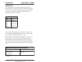
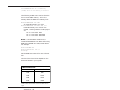
Differences between the 5025 and the 5025A
The 5025A is an enhanced version of the 5025. Various features of
the 5025 were improved upon to create the 5025A. See the table
below for a list of differences between these products.
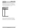
Differences Between the 5025 and the 5025A
Features
5025
5025A
Max. DRAM
4 MB
8 MB
SSD0 ROM size
128K
512K
SSD1 - max EPROM
1 MB
1 MB
SSD2 - max flash
SSD2 - max SRAM
SSD2 - max flash
SSD2 - max EPROM
SETUP EEPROM
DOS version
256K
512K
1.5 MB
512K
0K
512K
0K
1 MB
128 bytes
2048 bytes
5.0
6.22
Where to go from here:
Before you can begin developing your application program for the
5025A, we recommend you read Chapters 2–4. These chapters give
instructions for hardware installation, downloading and saving
your program, and autoexecuting your application.
Overview – 8
Chapter 2
Quick Start
Covers the basics of setting up
a 5025A system. This chapter
describes how to install the 5025A
into the card cage, how to establish a
serial communications link with your
PC and how to download files to the
5025A.
Chapter 3
RAMs & EPROMs
Configuring and installing static
RAMs and EPROMs. Installing the
battery backup and calendar/clock
module.
Chapter 4
SETUP
Running the SETUP configuration program.
Chapter 5
Save & Run Programs
How to save your program files
and autoexecute them from the
5025A.
Chapter 6
Serial Ports
Using COM1 and COM2. Setting
COM1 as the main console I/O for
serial communications with your PC.
Chapter 7
Watchdog Timer
Enabling the watchdog timer and
configuring the timeouts.
Chapter 8
LPT1 Printer Port
Using the LPT1 parallel port for a
printer, digital I/O, display or
keypad.
Chapter 9
Serial EEPROM
How to read and write to the serial
EEPROM.
Overview – 9
Chapter 10
Video and Keyboard
Configuring the 5025A with video
and a keyboard.
Chapter 11
External Drives
Configuring the 5025A with a floppy
drive or hard drive.
Chapter 12
Using Your Own DOS/OS
Configuring the 5025A with a version
of DOS/OS other than ROM-DOS.
Chapter 13
User-Defined Jumper
Configuring the user-defined jumper.
Chapter 14
CPU Power
Management
Using the SLEEP.COM and
SLOW.COM as power management
utilities.
Chapter 15
Troubleshooting
Problems encountered when using
the 5025A.
Chapter 16
Technical Data
Technical specifications, jumper
configurations and connector pinouts.
Appendix A
Software Utilities
Description and operation of
software utility programs and device
drivers.
Appendix B
Using non–Octagon cables, programming EPROMs, uploading files from
the 5025A and assigning drive
designators.
Overview – 10
CHAPTER 2
QUICK START
This chapter covers the basics of setting up a 5025A system and
tells you:
1.
How to panel mount or install the 5025A into the card cage;
2.
How to set up a serial communications link between the 5025A
and your PC; and
3.
How to download files to the 5025A and run a program from
the virtual drive.
WARNING:
The 5025A may not be installed in a PC. These
cards are designed to be independent CPU cards
only, not accelerators or coprocessors.
HARDWARE INSTALLATION
Your 5025A Control Card can be installed in one of three ways:
1.
2.
3.
Plug it directly into a Micro PC card cage;
Use the optional PC mounting bracket and plug it into any
passive backplane;
Panel mount it using the four mounting holes.
Panel Mounting the 5025A
To panel mount the 5025A, you will need the following equipment
(or equivalent):
5025A Control Card
5V Power Supply
VTC–9F Cable
Null modem adapter
5025A ROM–DOS & Utility Software Disk
PC SmartLINK w/manual
Your PC
If you are panel mounting the 5025A, a screw terminal connector
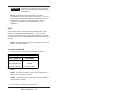
(P2) is provided to supply the 5V power. Refer to Figure 2–2 for
the location of various connectors.
Quick Start – 11
1.
Use #4–40 standoffs and screws to bolt down the 5025A.
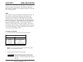
The following diagram shows the center to center mounting hole dimensions.
A
B
A = 4.90 in. (124,46 mm)
B = 0.20 in. (5,08 mm)
C = 3.50 in. (88,90 mm)
D = 0.10 in. at 45°, 2 PLCS
(2,54 mm at 45°)
E = 0.475 in. (4,44 mm)
F = 0.85 in. (21,59 mm)
G = 3.20 in. (81,28 mm)
H = 0.30 in. (7,62 mm)
J = 4.20 in. (106,68 mm)
J
K = 0.20 in. (5,08 mm)
0.125 in. HOLE
(3,17 mm)
4 PLCS
C
0.015 in. at 45• CHAMFER, 2 PLCS
(0,038 mm)
A31
A1
H
K
F
G
F
E
D
BEVEL CARD EDGE, 2 PLCS
.015 in. x 45• (0,038 mm x 45•)
Figure 2–1—5025A Center to Center Hole Dimensions
2.
Connect the proper ground and 5V wires to the terminal
block at P2.
3.
Connect one end of the VTC–9F cable to the null modem
adapter. Connect the other end to COM1 (J2) on the
5025A.
NOTE: You must use COM1 on the 5025A in order to
establish a serial communications link with your PC.
4.
If your PC has a 9–pin serial connector, connect the null
modem adapter to serial port COM1 or COM2 on your PC.
If your PC has a 25–pin serial connector, attach a 9–to
25–pin adapter to your null modem adapter, then insert
the matching end of the 9– to 25–pin adapter into COM1
or COM2.
Quick Start – 12
NOTE: Please refer to the PC SmartLINK manual for
more information on using COM2 on your PC.
You are now ready to transfer files between your PC and the
5025A. Please continue with the section, Establishing Communications with the 5025A in this chapter.
Using a Micro PC Card Cage
To install the 5025A in a Micro PC card cage, you will need the
following equipment (or equivalent):
5025A Control Card
Micro PC Card Cage
Power Module
VTC–9F Cable
Null modem adapter
5025A ROM–DOS & Utility Software Disk
PC SmartLINK w/manual
Your PC
Please refer to Appendix B if you are making your own serial cable
or using other non–Octagon components.
To install the 5025A:
1.
Please refer to Figure 2–2 for the location of various connectors
before installing the 5025A Control Card.
Quick Start – 13
RS–485
Port
RS–485
Termination
Jumpers
SSD2 Device
Type Select
SSD1 Device
Type Select
T–
T+
R–
Reset
U8
U7
U6
User
Option
R+
W1
W8
W2
Watchdog
Timeout
W12
W6
RS-485
2/4 Wire
U18
W7
W13
U5
IRQ
Jumper
U4
SSD-1
U17
SSD-2
U16
BIOS/DOS
SSD–0
U12
CPU
W9
U3
U33
Interrupt
Select
U32
U31
U2
80387
Coprocessor
Socket
U1
5V Only
Operation
U14 W3
W5
U13
COM2
RS–232/RS–485
Selector
= Pin 1
J1
LPT1
Printer Port
Boot Mode
Options
COM2
Serial Port
Keyboard/
Speaker Port
W4
J5
Y2
+5
GND
J3
U15
U22
J2
COM1
Serial Port
Battery
Connector
Battery Backup
Select Jumper
for SSD-2
AT Keyboard
Controller
Figure 2–2 – 5025A Component Diagram
WARNING:
WARNING:
The 5025A Control Card contains static–sensitive
CMOS components. The greatest danger occurs
when the card is plugged into a card cage. The
5025A card becomes charged by the user, and the
static discharges to the backplane from the pin
closest to the card connector. If that pin happens
to be an input pin, even TTL inputs may be
damaged. To avoid damaging your card and its
components:
•
Ground yourself before handling the 5025A
card.
Quick Start – 14
•
Disconnect power before removing or inserting the card.
When programming a memory device, place
the device in the socket before applying
power.
•
WARNING:
Take care to correctly position the 5025A card in
the card cage. The VCC and ground signals must
match those on the backplane. Figure 2–3 shows
the relative positions of the 5025A card as it is
installed in the card cage.
A31
B31
Card Edge Pins
A31 & B31
5025A Control
Card
Micro-PC
Motherboard
A1
B1
Card Edge Pins
A1 & B1
Figure 2–3 – Edge Connector Orientation
2.
Attach the power module to the card cage following the
instructions supplied with the power module.
3.
Make sure power to the card cage is OFF.
4.
Slide the 5025A into the card cage. The ROM–BIOS label on
the card should face to the left or up depending on the type of
card cage.
WARNING:
Plugging the card in incorrectly will destroy
the card!
Quick Start – 15
5.
Connect one end of a VTC–9F cable to the null modem adapter.
Connect the other end to COM1 (J2) on the 5025A.
NOTE: You must use COM1 on the 5025A in order to establish a serial communications link with your PC.
6.
If your PC has a 9–pin serial connector, connect the null
modem adapter to serial port COM1 or COM2 on your PC. If
your PC has a 25–pin serial connector, attach a 9– to 25–pin
adapter to your null modem adapter, then insert the matching
end of the 9– to 25–pin adapter into COM1 or COM2.
NOTE: Please refer to the PC SmartLINK manual for more
information on using COM2 on your PC.
ESTABLISHING COMMUNICATIONS WITH THE 5025A
1.
Install PC SmartLINK (or other communications software) on
your PC if you have not already done so. Refer to the PC
SmartLINK manual for installation instructions.
2.
Copy the 5025A files from the 5025A utility disk to a
subdirectory on your PC hard drive.
C:
MD \MPC
XCOPY A:\*.* \MPC /S
3.
Start PC SmartLINK. You are now ready to establish communications between your PC and the 5025A Control Card.
4.
Power on the 5025A.
5.
A logon message similar to the one below will appear on your
PC monitor:
Octagon 5025A-486-25MHz-2MB BIOS Vers. x.xx
Copyright (c) 1992-1994 Octagon Systems Corp. (TM)
All Rights Reserved
640K BASE RAM
384K SHADOW RAM
1024K EXTENDED RAM
Quick Start – 16
Starting ROM-DOS
5025A MEMDRIVE.SYS V2.01,
5025A MEMDRIVE.SYS V2.01,
(1024KB) as drive D:
5025A MEMDRIVE.SYS V2.01,
5025A MEMDRIVE.SYS V2.01,
extended memory present
formatting extended memory
memory device not found in SSD1
memory device not found in SSD2
C:\>path . . .
C:\>prompt . . .
5025A C:\>showtime . .
5025A C:\>
If you do not get the proper logon message:
6.
•
Check the serial parameters of your PC to make sure they
are set correctly. Parameters should be 9600 baud, 8 data
bits, no parity, and 1 stop bit.
•
Make sure a video card is not installed in the card cage.
•
Make sure all jumpers are set to factory defaults.
•
If the system still does not respond, refer to Chapter 15,
Troubleshooting.
Use the directory command to make sure your equipment and
software are working properly. Enter:
DIR
A directory listing of ROM–DOS files stored in the BIOS
socket should appear:
Volume in drive C is BIOS DRIVE
Directory of C:\
COMMAND
FAST
RESET
SETUP
SHOWTIME
SLOW
DISKSAVE
TRANSFER
CONFIG
MEMDRIVE
AUTOEXEC
COM
COM
COM
COM
COM
COM
EXE
EXE
SYS
SYS
BAT
27,095
366
378
2,918
619
366
21,478
9,969
118
4,682
50
11 file(s)
05–20–96
10–06–94
10–06–94
10–06–94
10–06–94
10–06–94
10–06–94
01–05–93
05–17–94
10–06–94
10–06–94
6:00a
11:18a
11:32p
11:18a
11:18a
11:18a
11:04a
2:36p
10:42a
11:18a
4:20p
68,039 bytes
0 bytes free
Quick Start – 17
7.
You are now ready to transfer files between your PC and the
5025A.
TRANSFERRING FILES BETWEEN 5025A & YOUR PC
Once you have established communications between your PC and
the 5025A, you can download files to the virtual drive on the
5025A. The virtual drive provides temporary storage for your files
until you save them to a flash memory or battery–backed static
RAM drive. The virtual drive also allows you to test and debug
your application files before permanently saving them.
You can also upload files from your 5025A to your PC for editing
and debugging. When booting from the BIOS drive, the
MEMDRIVE.SYS driver allocates a virtual drive. The size of the
virtual drive depends on the memory configuration of the 5025A:
5025A Virtual Drives
DRAM Installed
Virtual Drive Size
1 MB
384K uses MEMDRIVE.SYS EMS
2 MB
1024K uses MEMDRIVE.SYS EMS
4 MB
3072K uses MEMDRIVE.SYS EMS
8 MB
7168K uses MEMDRIVE.SYS EMS
A utility program called TRANSFER.EXE resides on the BIOS
drive and is used to send or receive files via COM1 of the 5025A.
TRANSFER.EXE uses the XMODEM protocol, as does PC
SmartLINK. The following information on downloading files
between the 5025A and your PC uses an example program,
DEMO.EXE and DEMO.BAS. These files are on your 5025A
utility disk in the DEMO subdirectory.
Downloading Files to the 5025A
The following procedures assume you are using PC SmartLINK
and is included in your directory path. For other communication
programs, refer to information on sending a file from your PC to
the target system.
Quick Start – 18
1.
Log into the directory on your PC which contains the file(s) you
will download to the 5025A. For example:
C:\MPC\5025A\DEMO
2.
Start PC SmartLINK and power on the 5025A.
3.
Execute the TRANSFER.EXE program from the 5025A by
entering:
TRANSFER D:DEMO.EXE
The following message displays:
Receiving D:DEMO.EXE
4.
Execute the following steps in PC SmartLINK:
a. Press <ALT> + <D> to download a file.
b. Type in the name of the file to transfer, e.g., DEMO.EXE.
c. Press ENTER to start (default). The progress of the
transfer displays in the dialog box.
NOTE: Transfer will timeout if the program has not been
started after approximately 40 seconds. It displays the
following message:
Failed to receive d:DEMO.EXE
Deleting d:DEMO.EXE
5.
When the transfer is complete, type the following DOS command to view the virtual drive directory and confirm that your
file has transferred to the 5025A:
DIR D:
The system will display the contents of drive D:
Volume in drive D has no label
Directory of D:\
DEMO
6.
EXE
27,264 01–01–80
2:57p
1 file(s) 27,264 bytes
To execute the program you have just downloaded, type:
D:DEMO
7.
The system displays a message on your PC.
Quick Start – 19
This page intentionally left blank.
Quick Start – 20
CHAPTER 3
RAMs AND EPROMs
Before you can save and boot your application from the 5025A, you
must first configure the system for your particular application
requirements. The 5025A card includes two sockets for solid–state
disks: SSD1 and SSD2.
SSD1
SSD1 generally contains the program to be executed on power–up.
The program is automatically loaded into DOS memory and
executed. SSD1 accepts either 128K/256K 12V flash memory,
128K/512K 5V flash memory, or 512K/1 MB standard EPROMs.
With flash memory, your application program can be saved using
the on–card programmer. These devices are erased automatically
during the programming process. You can write to the flash
memory a limited number of times (about 10,000), if your application program requires changes. With standard EPROMs, you must
use an offcard programmer. Refer to Appendix B for information
on programming standard EPROMs.
To Install an EPROM
1.
Set the jumpers at W8 for the correct memory device:
W8: SSD1 Memory Device Select
Pins Jumpered
Description
[1-3][2-4]
12V Flash memory
[3-5][4-6]
EPROM
[2-4][7-8]*
5V Flash memory
* = default
NOTE: You must use SETUP.COM to set the SSD1 device
before it can be properly accessed.
2.
Install the flash memory into socket SSD1.
WARNING:
When installing the chip, be sure to match
the notch in the chip with the notch in the
silkscreen. Incorrect installation will destroy
the chip!
RAMs and EPROMs – 21
WARNING:
Installing a 5V flash with 12V jumpers will
destroy the flash when DISKSAVE attempts
to program it!
NOTE: If installing a new flash memory, the driver
MEMDRIVE.SYS will report “Device not present”. You must
program the EPROM using the program DISKSAVE before
the EPROM is recognized. Refer to Chapter 5, Saving
Program and Support Files and MEMDRIVE.SYS in
Appendix A.
SSD2
SSD2 accepts 128K or 512K static RAMs, 128K/512K 5V flash
memory, or 512K/1MB standard EPROMs. A 3.6V AT clock
battery can be used to battery back a static RAM device in SSD2
via jumper block W4 or a DS–1213DM battery backup module may
be used.
NOTE: The DS–1213DM backs up only the RAM and not the
DATE and TIME functions.
To Install an EPROM
1.
Set the jumpers at W12 for the correct memory device:
W1 2: SSD2 Device Select
Pins Jumpered
Description
[2-4][3-5][7-8][9-10]*
RAM
[1-2][4-6][8-10][9-11]
EPROM
[2-4][5-7][8-10][9-11]
5V Flash memory
* = default
NOTE: You must use SETUP.COM to set the SSD2 device
before it can be properly accessed.
NOTE: Jumper W4[2-3] should be set if using an EPROM or
a flash memory in SSD2.
2.
Install the flash memory into socket SSD2.
RAMs and EPROMs – 22
WARNING:
When installing the chip, be sure to match
the notch in the chip with the notch in the
silkscreen. Incorrect installation will destroy
the chip!
NOTE: If installing a new flash memory, the driver
MEMDRIVE.SYS will report “Device not present”. You must
program the EPROM using the program DISKSAVE before the
EPROM is recognized. Refer to Chapter 5, Saving Program
and Support Files and MEMDRIVE.SYS in Appendix A.
To Install Static RAMs
1.
For static RAMs without battery backup, install the static
RAM directly into SSD2.
WARNING:
When installing the chip, be sure to match
the notch in the chip with the notch in the
silkscreen. Incorrect installation will destroy
the chip!
WAR
NING:
To Install Battery Backup for SSD2
•
The 3.6V clock battery can be used to battery back SSD2.
Jumper block W4[2-3] battery backs both the calendar/clock
and SSD2:
W4: RTC/SSD2 Battery Jumper
Pins Jumpered
Description
[1-2]*
Battery backup for calendar/clock.
No battery backup for SSD2.
[2-3]
Battery backup for calendar/clock
and SSD2.
* = default
or
•
Install a DS–1213DM into socket SSD2. Insert the static RAM
on top of the DS–1213DM.
NOTE: The DS-1213DM module will only battery back the
SSD2 in the module. The calendar/clock will not be backed up.
WARNING:
When installing the chip, be sure to match
the notch in the chip with the notch in the
silkscreen. Incorrect installation will destroy
the chip!
RAMs and EPROMs – 23
This page intentionally left blank.
RAMs and EPROMs – 24
CHAPTER 4
SETUP
DESCRIPTION
The SETUP program defines the 5025A system parameters. It is
shipped with default configuration parameters stored in the
EEPROM, U33. Changes are made by running the SETUP
program. The SETUP program is stored on the BIOS drive and on
the 5025A utility disk.
5025 A SETUP
Parameters
COM1 Console
Baud Rate
Power-on
Memory Test
Description
Specifies communications rate
between your PC and the
5025A when no video card is
in use.
Extensive memory testing
performed on bootup.
Default
9600
Enabled
SSD1 Device
Specifies the type of memory
device installed in SSD1.
512K 5V Flash
memory
SSD2 Device
Specifies the type of memory
device installed in SSD2.
128K/512K
SRAM
Boot from
Specifies the default boot
drive.
Number of
Floppy Drives
Specifies the number of floppy
drives attached.
Floppy Drive
Size
Number of hard
drives
Specifies size of the first
floppy drive.
The system will shadow
(write protect) this segment of
RAM.
The system will shadow
(write protect) this segment of
RAM.
Copies the contents of the
BIOS drive into high memory
freeing memory address
EXXX.
System will automatically
check to verify if a device is
attached.
Specifies the number of hard
drives attached.
Drive 0
parameters
Specifies the cylinders, heads
and sectors of hard drives.
Shadow
0C000H-0C7FFH
Shadow
0C800H-0CFFFH
Move BIOS
DRIVE high
Number of line
printers
SETUP – 25
BIOS drive
using ROM-DOS
0
1.44 MB
Yes
Yes
Yes
Auto check
0
Varies with
each drive
If you are running SETUP for the first time and have not previously saved and autoexecuted your program, we recommend you
keep the default setting, “Boot from: BIOS drive using ROM–
DOS”. The 5025A continues to boot from the BIOS drive until you
have verified that your program files are successfully saved to
SSD1. You can also test your program before setting the system to
boot from your AUTOEXEC.BAT file. Once your program is tested
and verified, you can run SETUP to configure the system to
autoexecute your program.
RUNNING SETUP
1.
Make sure you have established a serial communications link
between the 5025A and your PC.
2.
Type:
C:SETUP
NOTE: If you are not booting from the BIOS drive, the drive
designator may differ.
3.
The system will display the 5025A setup parameters and
available options. Select the option by pressing the space bar
until the correct information appears, then press <ENTER>.
Press <ESC> if you want to exit setup without saving your
responses.
•
COM1 Console Baud Rate:
1200
2400
4800
9600
19200
38400
57600
115200
The following messages may appear:
SETUP – 26
NOTE: To use COM1 as the console at a speed
other than 9600 baud, you must install the
BIOS boot jumper. (W3[3–4])
•
Power on memory test:
Enabled
Disabled
You may want to disable the memory test to speed up the boot
process.
•
SSD1 device:
none
128K 12V FLASH
256K 12V FLASH
128K 5V FLASH
512K 5V FLASH
EPROM (27C0X0)
WARNING:
•
(28F010)
(28F020)
(29F010/29C010/29EE010)
(29F040/29C040/28SF040)
Using a 5V flash in SSD1 and setting SSD1 to
12V flash DISKSAVE can destroy the flash!
SSD2 device:
none
128K/512K SRAM
128K 5V FLASH (29F010/29C010/29EE010)
512K 5V FLASH (29F040/29C040/28SF040)
512K EPROM (27C040)
1 MB EPROM (27C080)
NOTE: After setting the SSD1/SSD2 device, use DISKSAVE/
DISKSEND to program the flash EPROMs. The message
"Device not found from MEMDRIVE.SYS" displays until the
device is programmed.
NOTE: MEMDRIVE.SYS will also display "Device not found"
if the SSD2 device has not been set correctly.
•
Boot from:
BIOS drive using ROM–DOS
SSD1 using ROM–DOS
Floppy or Hard drive
SSD1 using User supplied DOS/OS
SETUP – 27
NOTE: If NONE was selected for the SSD1 device type, the
SSD1 boot options are not available.
We recommend that you do not change this option until you
have saved and verified your program files in SSD1. If booting
from the BIOS drive, the No Video jumper, W3[1–2], is
ignored. If jumper W3[3–4] is not installed and you selected
an option other than “Boot From BIOS Drive Using ROM–
DOS”, the following message appears:
NOTE: To boot from the specified device you
must install the BIOS boot jumper. (W3[3-4])
•
Number of floppy drives:
0, 1, 2
A maximum of 1 floppy drive is possible if booting from SSD1
and using your own DOS. See Chapter 12, Using Your Own
DOS/OS for details. The following message will appear if you
select one floppy disk and you boot from SSD1 with your own
DOS:
NOTE: Connect the floppy to the second floppy
connector. The drive will be known as B:
•
Floppy drive 1 size:
360K
1.2 MB
720K
1.44 MB
•
Floppy drive 2 size:
360K
1.2 MB
720K
1.44 MB
These two options only display if you have specified that a
floppy drive(s) is attached to the 5025A.
SETUP – 28
•
Shadow 0C000H–0C7FFH
Yes
No
This address is usually reserved for the video BIOS.
•
Shadow 0C800H–0CFFFH
Yes
No
This address is usually reserved for hard disk drives, SCSI
controllers, etc. The system defaults to shadowing RAM (write
protecting) which enhances performance. However, some
peripheral cards require access to RAM at these locations.
Please refer to your peripheral card manual for specific
information regarding RAM address locations.
NOTE: The shadow RAM options will not display on 512K or
1 MB DRAM systems.
•
Move BIOS DRIVE high:
Yes
No
You may enable the system to copy the BIOS drive (normally
at E000–F000) into extended memory on systems with 1 MB or
more DRAM. This “frees” up the address space for other
applications such as PCMCIA, SCSI and network cards.
NOTE: This option does not display on 512K systems.
•
Number of line printers:
Auto Check
0
1
2
3
If you select Auto Check, the system automatically checks the
LPT1 printer port to verify that a printer is available by
writing a pattern to the printer data lines during boot–up or
reset. If you have a non–printing device attached to the LPT1
port, e.g. MPB–16PC and do not want data written to that port
during boot–up, deselect the Auto Check option.
SETUP – 29
Number of hard drives
0
1
2
Drive 0 parameters
Cylinders (xxx):
Heads (x):
Sectors (xx):
Press ENTER to SAVE the changes or
Press ESC to EXIT without saving the changes.
Options saved.
Depending on the options you have selected, the system may
display the following message:
You must reset for these options to take effect.
SETUP EXAMPLE
The following example configures a system with 256K 12V flash
EPROM in SSD1, nothing in SSD2, no memory test, 9600 baud, no
hard drives, and booting from SSD1 with ROM–DOS:
OCTAGON SYSTEMS CORPORATION
5025A SETUP UTILITY V3.2
(Press SPACE to CHANGE, ENTER to ACCEPT, ESC to
EXIT)
COM1 Console Baud Rate: 9600
Power on memory test: Disabled
SSD1 device: 256K 12V FLASH (28F020)
SSD2 device: None
Boot from: SSD1 using ROM–DOS
Number of floppy drives: 0
Shadow 0C000H–0C7FFH: Yes
Shadow 0C800H–0CFFFH: Yes
Move BIOS DRIVE high: Yes
Number of line printers: Auto check
Number of hard drives: 0
Press ENTER to SAVE the changes or
Press ESC to EXIT without saving the changes.
Options Saved.
You must reset for these options to take effect.
C:\
SETUP – 30
CHAPTER 5
SAVE & RUN PROGRAMS
SAVE AND RUN YOUR PROGRAMS ON THE 5025A
Once you have written, tested and debugged your application, you
can then save it to either battery–backed static RAM or flash
memory in SSD2 or save it to flash memory in SSD1. When you
reboot the 5025A, your program will automatically load into DOS
memory and execute. (You can only boot from SSD1.)
This chapter tells you:
1. How to save an application program to SSD1;
2.
How to autoexecute the program from the 5025A; and
3.
How to override autoexecution of your program.
The information in this chapter assumes you will be using ROM–
DOS in your application. Some Microsoft programs make undocumented DOS calls. With ROM–DOS, an error will be returned
when an undocumented DOS call is made, causing your program to
operate erratically. We recommend booting from SSD1, using your
own DOS, when using programs with undocumented DOS calls.
Refer to Chapter 12, Using Your Own DOS/OS, for more information on saving and autoexecuting programs.
This chapter also assumes you will be using the 5025A without a
video card/monitor. If you are using these devices, refer to Chapter 10, Video and Keyboard, for more information on transferring
and saving programs.
SAVING PROGRAM AND SUPPORT FILES
In addition to your application program, you must also transfer
support files to the 5025A to ensure proper operation. These files
include the ROM–DOS COMMAND.COM, CONFIG.SYS,
AUTOEXEC.BAT and other files and device drivers specific to your
application. ROM–DOS COMMAND.COM is required to boot the
5025A with ROM–DOS from SSD1. AUTOEXEC.BAT defines the
routine for autoexecution of your program.
CONFIG.SYS defines the various device drivers of your 5025A
system. The following is an example listing of CONFIG.SYS
entries for the device drivers included with the 5025A. Each of
Save & Run Programs – 31
these device drivers is discussed in greater detail in Appendix A,
Software Utilities. Refer to Appendix B for more information on
how the 5025A assigns drive designators:
Accesses the SSD1 drive
Accesses the SSD2 drive
Accesses the BIOS drive
Accesses the virtual drive in
extended memory
DEVICE=MEMDRIVE.SYS BASE 136 Accesses a virtual drive in DOS
base memory
DEVICE=MEMDRIVE.SYS
DEVICE=MEMDRIVE.SYS
DEVICE=MEMDRIVE.SYS
DEVICE=MEMDRIVE.SYS
SSD1
SSD2
BIOS
EMS
NOTE: We recommend you include in your CONFIG.SYS file the
entry DEVICE=MEMDRIVE.SYS BIOS. This allows you to easily
access utility programs (SETUP, TRANSFER, etc.) that are located
on the BIOS drive.
To Save Files to the 5025A SSD1
The following information steps you through transferring, saving
and autoexecuting a program using the DEMO application and a
flash memory in SSD1. All the files for this application are located
on the 5025A utility disk in the DEMO directory. These procedures
assume you are using PC SmartLINK. The two programs,
DISKSAVE and DISKSEND, transfer and save the files on the
floppy disk to SSD1. The DISKSAVE program resides on the BIOS
drive of the 5025A and the DISKSEND program resides on the
5025A utility disk.
1.
Do an XCOPY of the utility disk to your hard drive. This will
copy all subdirectories on the utility disk.
MD C:\MPC
XCOPY A:\*.* C:\MPC /S
2.
Change to the 5025A directory to allow access to DISKSEND:
CD \MPC\5025A
3.
Connect a serial cable between COM1 on the 5025A to a COM
port on your PC.
Save & Run Programs – 32
4.
Start PC SmartLINK and power on the 5025A.
NOTE: If you are using PC SmartLINK from COM2 on your
PC, you must use the /C2 switch with DISKSEND. Refer to
the DISKSEND section in Appendix A for more information.
Also, if you cannot communicate at 38400 baud, use the /Bxxx
switch on both DISKSAVE and DISKSEND.
5.
On the 5025A, execute the DISKSAVE program by typing:
A>DISKSAVE /X /DSSD1
The systems displays the following message:
Attempting connection with DISKSEND on remote
host.
6.
Exit to DOS and type the following:
C>DISKSEND \MPC\DEMO
The system then erases and programs the flash memory. This
takes several minutes.
7.
Restart PC SmartLINK.
8.
If you are saving your program to SSD1 for the first time or
you are running the DEMO program, the system should boot
from the BIOS drive since you did not change the default
“Boot from” option in SETUP. Type:
RESET
9.
Display and verify the contents of SSD1:
DIR E:
10. Test run the DEMO program:
E:DEMO
11. If you want to boot from SSD1, run SETUP to specify this
option.
Save & Run Programs – 33
AUTOEXECUTING YOUR PROGRAM
Once you have saved your program and other files to SSD1 you
may boot from SSD1 and autoexecute your program. You cannot
boot from SSD2.
1.
Make sure jumper W3[3–4] is installed. (This is the default
setting.)
2.
Establish a serial communications link between your PC and
the 5025A.
3.
Make sure the name of your application program is listed in
the AUTOEXEC.BAT file, e.g. DEMO.
4.
Run SETUP and specify “Boot from: SSD1 using ROM–DOS”.
SETUP
5.
Type:
RESET
The 5025A will reset and boot from SSD1. SSD1 now becomes
drive A.
OVERRIDING PROGRAM AUTOEXECUTION FROM
SSD1
If you want to make changes to your program and need to override
autoexecution of your program, you must reboot the 5025A from
the BIOS drive. There are two options available:
1.
You can rerun SETUP to change the “Boot from” option to
“BIOS drive with ROM–DOS”. If you included the line
DEVICE=MEMDRIVE.SYS BIOS in your CONFIG.SYS file,
you can access the SETUP program on the 5025A BIOS drive.
2.
You can remove jumper W3[3–4]. However, this may be
inconvenient and/or impossible if you are making program
changes from an off–site location.
Save & Run Programs – 34
Running SETUP Again
1.
Make sure you have established a serial link between your PC
and the 5025A.
2.
To execute SETUP which is on the BIOS drive, type:
E:SETUP
NOTE: The drive designator will vary depending on the
hardware configuration of the 5025A.
3.
Select the “Boot from BIOS drive using ROM–DOS” option.
4.
Type:
E:RESET
5.
Make the necessary changes to your application and copy the
new files to a floppy disk or RAM disk.
6.
Rerun DISKSEND and DISKSAVE to save your new files to
SSD1. Verify and test your program.
7.
Rerun SETUP to change the default boot drive to “SSD1 using
ROM-DOS”.
8.
Reset the 5025A.
Removing Jumper W3[3–4]
If the SETUP program is not accessible from SSD1, you must
remove jumper W3[3–4].
If you do not have a video card installed, the video display is
through a COM1 serial link to your PC. The 5025A boots from the
BIOS drive using ROM–DOS. COM1 is configured for 9600,
N, 8, 1.
Save & Run Programs – 35
If you have a video card installed in your 5025A systems, removing
W3[3–4] will boot the 5025A from the BIOS drive and you will
continue to use the video installed in your system.
The following message appears when you reboot the 5025A:
BIOS boot jumper (W3[3–4]) not installed, booting from the BIOS drive and ignoring the video
jumper setting.
.
.
5025A A:\>
After booting from the BIOS drive, use the DISKSAVE and
DISKSEND programs to download new files to SSD1. Before
rebooting the 5025A, be sure to reinstall jumper W3[3–4] if you
want the 5025A to boot a device other than the BIOS drive.
Save & Run Programs – 36
CHAPTER 6
SERIAL PORTS
DESCRIPTION
The 5025A has two serial ports that use a high performance
16C550 communications controller, which is Intel 8250 compatible.
They can be used for interfacing to a printer, terminal or other
serial device. These ports support 5–, 6– 7–, or 8–bit word lengths,
1, 1.5, or 2 stop bits, and baud rates up to 115.2K.
J2: COM1 and J1: COM2
Serial Ports
Pin #
Function
1
DCD
2
DSR
3
RxD*
4
RTS
5
TxD*
6
CTS
7
DTR
8
RI
9
Gnd
10
+5V
* = active low
Use a VTC–9F cable to connect the ports to the external serial
equipment. The pinout of the connector allows you to plug the
cable directly into a 9–pin PC serial connector. When interfacing
the 5025A to your PC, you will need to use a null modem adapter.
Serial Ports – 37
COM1 AS CONSOLE I/O
The default settings for the 5025A are as follows:
•
•
W3[1–2] — COM1 used for console (no video card)
W3[3–4] — Boot using parameters defined by SETUP
W3: COM1, Video and BIOS Boot Options
Pins Jumpered
Video
System
Video over COM1. System will boot
SETUP boot device.
[1-2][3-4]*
[1-2]
No video card
installed in
system.
[3-4]
[3-4]†
[3-4] not jumpered†
Description
Video card
installed in
system.
Video over COM1. System will boot
BIOS drive.
No COM1 video available. COM1
available for use in application.
System will boot SETUP boot
device.‡
Video on CRT. System will boot
SETUP boot device.
Video on CRT. System will boot
BIOS drive.
* = default
† = W3[1-2] is ignored
‡ = If SETUP boot device is BIOS drive, system will use video over COM1.
NOTE: When W3[3–4] is removed, the baud rate defaults to 9600
and the TRANSFER program defaults to COM1 as the main
console port.
Some programs which access the video memory directly will not
work properly on the 5025A without a video card resident. Refer
to the DEMO.BAS program on the utility disk for an example of
required QuickBASIC modifications. Refer to Chapter 10, Video
and Keyboard, for more information on using a video as the
console.
Serial Ports – 38
COM1 AS RS-232 I/O
When you have completed developing your application and programmed the 5025A, you can use COM1 as an RS–232 serial port
for connection to a printer, modem or other serial device. To access
COM1 you have two options:
1.
Configure the 5025A for no console port by removing jumper
W3[1–2] and boot the system from SSD1 or floppy/hard drive
(not the BIOS drive). If you do not remove W3[1–2], the BIOS
sign on messages will be sent to your printer, modem or other
device connected to COM1.
2.
Add a video card and monitor to your 5025A system.
Use a VTC–9F cable to connect the ports to the external serial
equipment. The pinout of the connector allows you to plug the
cable directly into a 9–pin PC serial connector.
COM2 AS RS-422/485 I/O
COM2 is jumper selectable for either RS–232 or RS–485 communications at W5. Make sure W5[1-2] is jumpered for RS-485 prior to
using the port.
W5: RS-232 or RS-485 Select
Pins
Jumpered
Description
[1-2]
RS-485 Receiver selected
[2-3]*
RS-232 Receiver selected
* = default
You can connect up to 32 units on a multidrop RS-485 network.
However, only one transmitter can be active at a time. Although
no wire type or maximum wire length is specified in the EIA 485
specification, the EIA 422 specification (which is very similar) lists
a maximum length of 4000 feet.
Serial Ports – 39
The RS-422/485 compatible port is accessed through COM2 via
terminal block P3. This port will support two–wire or four–wire
transmissions. The following diagrams show how a typical two–
wire or four–wire mode network is implemented:
RS-422/485
2 Wire (Half Duplex) Transmission
T+
TR+
R-
T+
TR+
R-
Node 1
Node 4
T+
TR+
R-
T+
TR+
R-
Node 2
Node 3
Figure 6–1—Two–Wire Network
Serial Ports – 40
RS-422/485
4 Wire (Full Duplex)
Transmission
T+
TR+
R-
Host
Node 1 T+
T+
TR+
R-
TR+
R-
T+
TR+
R-
Slave
Node 3
Slave
Node 2
Slave
Node 4
Figure 6–2—Four–Wire Network
Jumper block W7 selects either two or four wire transmission.
This jumper automatically disables the transmitter output when
operating in the two-wire mode.
W7: Two or Four Wire Select
Pins Jumpered
Description
[1-2]
Four wire transmission
[2-3]*
Two wire transmission
* = default
Operating Precautions
The transmitter and receiver are not optically isolated so you must
avoid ground loops. You should send only signals through the
RS-485 lines, not power or power grounds. Power grounds cannot
be used as a reference ground for RS–485 signals. Establish a
common ground reference before implementing your 485 network.
Serial Ports – 41
The maximum common mode voltage output is +/–7V. Refer to the
EIA 485 specification for further details on grounding and safety
procedures.
Transmitter Control
To turn the transmitter ON and OFF through software control,
refer to the following table:
5025A Transmitter Control
Program Statement
Description
Write a "1" to I/O location
20CH
Enables transmitter output
I/O location 20CH, 1
Write a "0" to I/O location
20CH
Disables transmitter output
I/O location 20CH, 0
Termination Network
Jumper block W1 installs or removes the termination network. A
termination network must be installed at the last receiver of the
network. Failure to do so may cause spurious oscillation on the
receive line and corrupt incoming data.
W1: RS-485 Receiver Termination
Pins Jumpered
Description
[1-3][2-4]
Termination active
[3-5][4-6]*
No termination
* = default
P3: RS-485 Connector
Pin #
Function
1
Transmit +
2
Transmit -
3
Receive +
4
Receive -
Serial Ports – 42
DISABLING INTERRUPTS
The PC Bus does not allow shared interrupts on the bus. You can,
however, disable the COM1 and COM2 interrupts (IRQ4 and
IRQ3) to allow for other devices which use these interrupts. If
COM1 is the console, its interrupt (IRQ4) is in use. COM2 (IRQ3)
is not used by the BIOS. To disable interrupts for COM1, write a 0
to 3FC bit 3. To disable COM2 write a 0 to 2FC bit 3.
However, the 5025A now supports three additional interrupts:
IRQ9, IRQ10 and IRQ11. Please refer to Appendix B for more
information.
USING QUICKBASIC TO COMMUNICATE VIA COM1
Several programming languages including QuickBASIC V4.5
assume a video card is present, and for system speed reasons write
directly to the video hardware. This can be a problem since many
control applications require video output. The following discussion
is directed at QuickBASIC, but the principles (not accessing the
print routines which access the video memory directly) apply to
many languages. There are several ways to use COM1 from
QuickBASIC V4.5.
Systems with a Video Card
Add a video card to the system and open/close COM1 using the
QuickBASIC OPEN/CLOSE commands.
Systems without a Video Card
WARNING:
The system will lock if you use commands such as
PRINT or PRINT USING. Because QuickBASIC
writes directly to video memory, these commands
are usually displayed on a monitor.
METHOD 1
The system display will not appear over COM1 while the BIOS
boots.
1.
Remove the video jumper W3[1–2].
Serial Ports – 43
2.
Boot from a drive other than the BIOS drive, e.g., SSD1 with
ROM–DOS.
3.
Use QuickBASIC’s OPEN/CLOSE/PRINT/INPUT commands
to access COM1. The following is an example program using
these commands:
OPEN "COM1:9600,N,8,1,BIN" FOR RANDOM AS #1
CRLF$=CHR$(13)+CHR$(10)
PRINT #1, "INPUT A STRING" + CRLF$
INPUT #1, A$
PRINT #1, CRLF$ + A$
CLOSE #1
NOTE: All PRINT/PRINT USING/INPUT . . . commands
MUST use the COM1 device number.
METHOD 2
1. Leave the video jumper W3[1–2] on.
2.
Use QuickBASIC’s OPEN/CLOSE/PRINT/INPUT commands
to access COM1. After closing the device, manually restore
the serial parameters. The following example assumes 9600,
N, 8, 1 parameters:
OPEN"COM1:9600,N,8,1,BIN" FOR RANDOM AS #1
CRLF$ = CHR$(13) + CHR$(10)
PRINT #1, "INPUT A STRING" + CRLF$
INPUT #1, A$
PRINT #1, CRLF$ + A$
CLOSE #1
NOTE: All PRINT/PRINT USING/INPUT . . . commands
MUST use the COM1 device number.
3.
Restore the serial parameters by using a batch file specifying
your program's name as the first line of the file and
COM1CON as the last line of the file.
For example, TEST.BAT includes the following to execute a
QuickBASIC V4.5 (or other language) application named
USECOM1:
USECOM1
COM1CON
Then execute TEST.BAT.
Serial Ports – 44
METHOD 3
1. Leave the video jumper W3[1–2] on.
2.
Use the PRINTS, PRINTSL, KEYHIT$, INKEY2$ commands
as found in the DEMO.BAS and DSQBTEST.BAS programs
(included on the utility diskette). Unformatted string output
and string input must be done manually.
NOTE: Programs written in this manner will also work with a
video card present and therefore systems can be “debugged” on
your PC.
METHOD 4
1. Use an off–the–shelf communications library.
2.
This may require restoring the COM1 parameters similar to
method 2, if the console video is expected after the
QuickBASIC program terminates.
METHOD 5
1. Use COM2 instead of COM1. This is similar to Method 1, but
you will still get the system displays over COM1.
Using Turbo C
If you need to restore the serial parameters after executing a C
program, refer to the file COMTEST.CPP. This file can be
downloaded from the Octagon bulletin board at (303) 427–5368
using 2400 baud, 8 data bits, no parity, 1 stop bit.
Serial Ports – 45
This page intentionally left blank.
Serial Ports – 46
CHAPTER 7
WATCHDOG TIMER
DESCRIPTION
The watchdog timer is a failsafe against program crashes or
processor lockups. It times out every 1.2 seconds unless reset by
the software. There are three timeout periods for the watchdog
timer. Each is selected by configuring jumperblock W2. As
shipped, the timeout is 1.2 seconds.
W2: Watchdog Timer
Pins
Timeout
Jumpered
[1-2]*
1.2 seconds
[2-3]
0.15 seconds
Not
jumpered
0.6 seconds
* = default
The address for the watchdog timer enable port is 380H. The
timer is software disabled when you write a “0” to address 380H.
This is the default setting on power–up or reset.
When you want to start using the watchdog timer, write a “1” to
address 380H. You must write any data to 201H within the
timeout period to prevent the board from resetting. When you
write to 201H, the timer resets and begins counting down again.
The following table lists the software enable and strobe information:
Watchdog Timer Software & Strobe Addresses
Enable Base Address 380H
Strobe Base Address 201H
Timer disables = 0*
Write any data to this address to
reset timer
Timer enabled = 1
* = default
Watchdog Timer – 47
This page intentionally left blank.
Watchdog Timer – 48
CHAPTER 8
LPT1 PRINTER PORT
DESCRIPTION
The LPT1 parallel port has a 20–pin connector. It can be used to
support a number of devices including PC compatible printer,
multiline display, matrix keypad or 17 digital I/O lines.
J5: Printer/Digital I/O Port
Pin #
Function
1
Out
STB*
2
Out
AFD*
3
I/O
0
4
In
ERR*
5
I/O
1
6
Out
INIT*
7
I/O
2
8
Out
SLIN*
9
I/O
3
10
I/O
4
11
I/O
5
12
I/O
6
13
I/O
7
14
In
ACK*
15
In
BUSY
16
In
PE
17
In
SLCT
18
+5
19
Gnd
20
Gnd
* = active low
LPT1 Printer Port – 49
PRINTER
To install a printer:
1.
Connect a CMA–20 cable from the LPT1 port (J5) to the
PSKI–1 interface card.
2
Connect your printer to the DB–25 connector on the PSKI–1.
DISPLAY
The LPT1 port supports either vacuum fluorescent (DP series) or
liquid crystal displays (LCD). To interface the displays to the
5025A, use the LCD–IFB interface board for LCD displays and the
DP–IFB interface board for the DP series displays. A CMA–20
cable is required to connect the interface board to the 5025A. The
program DISPLAY.EXE (found on the 5025A utility disk in the
\DISPLAY subdirectory) provides an easy method to use the
display. Please refer to the file DISPLAY.DOC on the utility disk
for information on how to initialize and use the display.
To install a display:
1.
Connect a CMA–20 cable from the LPT1 port to the DP–IFB or
LCD–IFB.
2.
Connect the display cable to the interface board.
3.
Refer to the file DISPLAY.DOC for more information on
initializing and using the display.
LPT1CON allows the display to be used as the console device. To
do this, add the DISPLAY and LPT1CON commands to your
AUTOEXEC.BAT file. Keyboard input can be from a local keyboard or from COM1 (if no video card is installed and if W3[1-2],
no video jumper, is installed).
NOTE: The DP style displays can also be driven from a serial port
when used in conjunction with Octagon’s SDA–1 Serial Display
Adapter.
LPT1 Printer Port – 50
KEYPAD
LPT1 also supports 4x4 matrix keypads. To interface the keypad
to the 5025A, use either the LCD–IFB or DP–IFB interface board.
A CMA–20 cable is required to connect the interface board to the
5025A. The program DISPLAY.EXE (found on the 5025A utility
disk) provides an easy method to use the keypad. Please refer to
the file DISPLAY.DOC on the utility disk for information on how
to initialize and use the keypad.
To install a keypad:
1.
Connect a CMA–20 cable from the LPT1 port to the DP–IFB or
LCD–IFB.
2.
Connect the keypad cable to the interface board.
3.
Refer to the file DISPLAY.DOC for more information on
reading the keypad.
DIGITAL I/O LINES
When used only for digital I/O, a CMA–20 cable connects the port
to a STB–20 terminal board for connection of field wiring. These
boards may be used for any low voltage digital signal. You can also
connect an Octagon MPB–16PC opto module rack to LPT1 to
control high voltage/high current lines. Please refer to the documentation for each of these products for more information.
LPT1 Printer Port – 51
This page intentionally left blank.
LPT1 Printer Port – 52
CHAPTER 9
SERIAL EEPROM
DESCRIPTION
Up to 1792 bytes (that is, 896 words) of user-definable data can be
saved in the serial EEPROM. The serial EEPROM does not
require battery backup to maintain the data when the system
power is off. The serial EEPROM is easily accessible via software
interrupts by most programming languages. The software interrupt used is INT 17 subfunction 0FEH (read) and INT 17
subfunction 0FFH (write).
READING THE SERIAL EEPROM
The following Borland C example reads word 2:
_AH = 0xfe;
/* read */
_BX = 2;
/* index for word in serial EEPROM (0-895)*/
_DX = 0xffff; /* always set to FFFFH */
geninterrupt(0x17); /* do interrupt */
EEdata = _AX; /* serial EEPROM data returned in AX */
WRITING TO THE SERIAL EEPROM
The following Borland C example writes 1234H to word 2:
_AH = 0xff;
/* write */
_BX = 2;
/* index for word in serial EEPROM (0-895)*/
_CX = 0x1234; /* Data to write */
_DX = 0xffff; /* always set to FFFFH */
geninterrupt(0x17); /* do interrupt */
NOTE: During programming of the EEPROM, the power LED
may momentarily flash.
Serial EEPROM – 53
This page intentionally left blank.
Serial EEPROM – 54
CHAPTER 10
VIDEO AND KEYBOARD
DESCRIPTION
You can use a video card with a monitor and a keyboard with the
5025A instead of using your PC keyboard and monitor over a serial
communications link. The speaker and keyboard lines are brought
out to a 10–pin connector via a CMA–10 cable. The Octagon
PSKI–1 interface provides a PC compatible connector for the
keyboard and provides screw terminals for the speaker. Any AT
compatible keyboard may be used.
This chapter tells you:
1.
How to use a video monitor and keyboard with a 5025A; and
2.
How to transfer files between your PC and a 5025A with a
video and keyboard only.
USING A VIDEO MONITOR AND KEYBOARD
You will need the following equipment (or equivalent) to use your
5025A with a video and keyboard:
5025A PC Control Card
Micro PC Card Cage
Power Module
54xx Video Card
AT Compatible Keyboard
PSKI–1 Interface Board
VTC–9F Cable
Monitor
CMA–10 Cable
1.
Configure the 5025A for a video card by installing jumper
W3[1–2]. Also configure the system to boot from the BIOS
drive.
2.
Connect the video card to the video monitor.
3.
Connect the PSKI–1 to J3 on the 5025A using a CMA–10 cable
and then connect the keyboard to the PSKI–1.
Video & Keyboard – 55
4.
Install the 5025A and video card into the card cage.
5.
Power on the 5025A. The BIOS messages should appear on
your video monitor:
Octagon 5025A-486-25MHz-2MB BIOS Vers x.xx
Copyright (c) 1992-1994 Octagon Systems Corp. (TM)
All Rights Reserved
Saving a Program to the 5025A
The following steps detail the procedures for transferring files to
the 5025A and programming the flash memory in SSD1 using the
DISKSEND and DISKSAVE programs. The DISKSAVE program
resides on the BIOS drive of the 5025A and the DISKSEND
program resides on the 5025A utility disk.
1.
Do an XCOPY of the utility disk to your hard drive:
MD C:\MPC
XCOPY A:\*.* C:\MPC /S
2.
Change to the 5025A directory to allow access to DISKSEND:
CD \MPC\5025A
3.
Connect a VTC–9F cable with a null modem adapter between
COM1 of your PC to COM1 of the 5025A.
4.
On the 5025A, execute the DISKSAVE program by typing:
C>DISKSAVE /DSSD1 /X
5.
From your PC, execute the DISKSEND program by typing:
C>DISKSEND \MPC\DEMO
The system will then erase and program the flash memory.
This will take several minutes.
Video & Keyboard – 56
Transferring Files to the 5025A
The following steps detail the procedures for transferring files from
your PC to the virtual drive on the 5025A. In order to transfer
files from your PC to the 5025A, you must execute the TRANSFER
program from both the 5025A and your PC.
1.
Connect a VTC–9F cable with a null modem adapter between
COM1 of your PC to COM1 of the 5025A.
2.
Execute the TRANSFER program from the 5025A to receive a
file from your PC.
TRANSFER /COM1 /R /V <drive>filename.ext
<drive> is the virtual drive on the 5025A where the file will be
transferred.
filename.ext is the name of the file on the 5025A which you
are receiving from your PC.
/V enables “R” characters upon receiving a block and “T” upon
transferring a block.
3.
Execute the TRANSFER program from your PC to send a file
to the 5025A.
TRANSFER /COM1 /S /V <drive><path>filename.ext
filename.ext is the name of the file on the PC which you are
sending to the 5025A.
NOTE: Transfer will timeout if the program has not been started
after approximately 40 seconds. It displays the following message:
Failed to receive <drive>filename.ext
Deleting <drive>filename.ext
Also, you may speed up the transfer using the /Bnnnn switch to
increase the baud rate. Example: /B57600.
Video & Keyboard – 57
Transferring Files from the 5025A
In order to transfer files from your PC to the 5025A, you must
execute the TRANSFER program from both the 5025A and your
PC.
1.
Connect a VTC–9F cable with a null modem adapter between
COM1 of your PC to COM1 of the 5025A.
2.
Execute the TRANSFER program from the 5025A to send a file
to your PC.
TRANSFER /COM1 /S /V filename.ext
filename.ext is the name of the file on the 5025A which you
are sending to your PC.
3.
Execute the TRANSFER program from your PC to receive a
file from the 5025A.
TRANSFER /COM1 /R /V filename.ext
filename.ext is the name of the file on the PC which you are
receiving from the 5025A.
NOTE: Transfer will timeout if the program has not been started
after approximately 40 seconds. It displays the following message:
Failed to receive <drive>filename.ext
Deleting <drive>filename.ext
Also, you may speed up the transfer using the /Bnnnn switch to
increase the baud rate. Example: /B57600.
Video & Keyboard – 58
CHAPTER 11
EXTERNAL DRIVES
DESCRIPTION
You can use your 5025A Control Card with one or two floppy disk
drives and a hard disk drive. This chapter includes installation
and operation instructions for each device. Also, refer to the
instruction manuals included with each device.
For each of the devices below, the first step is to install the 5025A
Control Card into the Micro PC backplane. Refer to the instructions in Chapters 4 – 5 if you will be booting from the BIOS drive
or from SSD1 using ROM–DOS. If you are booting up using your
own DOS, refer to the instructions in Chapter 12.
You can boot your 5025A from a floppy or hard disk. However,
MEMDRIVE.SYS must be placed in your CONFIG.SYS file in
order for the system to access the memory device in SSD1, SSD2
and the BIOS drive.
FLOPPY DISK DRIVES
You can add two floppy disk drives by using the 5800A Floppy/
Hard Disk Card with your 5025A card.
1.
Install the 5025A Control Card.
2.
Install the 5800A Floppy/Hard Disk Card and the 5814 Floppy
Disk Drive, following the instructions included with these
products.
3.
Plug the card cage power cable into an AC outlet. Turn on the
power supply. This supplies power to the floppy disk drive
(via the ribbon cable) as well as to the cards in the card cage.
4.
Run SETUP to set the number of floppy drives and their size.
NOTE: Two drive designators will be assigned regardless of
how many drives you specify in SETUP.
5.
When you boot from either the BIOS or SSD1 drives using
ROM–DOS, the floppy drive designations will be A: and B:.
External Drives – 59
NOTE: When you boot from SSD1 using your own DOS, only
one floppy drive will be available, since DOS thinks that SSD1
is drive A:. Connect your floppy disk drive to connector J3 on
the 5800A (FDC drive B) and access it with B:.
6.
If, in SETUP, you entered 0 drives, access to either A: or B:
will immediately generate an error message:
ABORT RETRY FAIL?
Press <A> or <F> to cancel your request.
If, in SETUP, you entered 1 drive, you can access drive A.
Requests to access drive B: result in the following prompt:
INSERT FLOPPY INTO DRIVE B: AND PRESS ANY KEY
Insert another floppy disk and press a key. The program then
accesses your one drive as drive B:. When another request for
drive A occurs, a prompt gives you the opportunity to replace
the original A: floppy. In this way, systems with only one
drive can copy files from one floppy to another.
If, in SETUP, you entered 2 drives, access to either drive A: or
drive B: work just as they would in a PC.
If you want to boot from the floppy disk using your own DOS refer
to Chapter 12, Using Your Own DOS/OS.
HARD DISK DRIVE
The 5800A Micro PC Floppy/Hard Disk Drive Cards support IDE
type hard drives. The disk drive designation for the first hard
drive will be C:. If you boot from ROM–DOS in SSD1 or the BIOS
drive, the ROM-DOS drive will be D.
External Drives – 60
Hard Drive SETUP
IRQ
No. of Drives
Setting in
in HDSETU P
HDSETU P
(502 5A)
No. of
Drives in
CPU SETUP
W 13 setting
0
NA
1-2
1-2 (IRQ14)
1-2
IRQ5
0
2-3 (IRQ5)
1-2
IRQ14
0
1-2 (IRQ14)
1-2
IRQx
1-2
See note 1
NOTE 1: The system will not operate correctly if both
HDSETUP.COM and SETUP have hard drives defined.
NOTE 2: If the 5815 BIOS is disabled via jumper, set W13 to 1-2
(IRQ14). See the 5815 manual for more information.
If the HD BIOS is enabled on the 5025A, be sure to disable the HD
BIOS on the 5800A or the 5815. For example,
To disable the 5800A HD BIOS, type the following:
5800A: HDSETUP drives = 0
To disable the 5815 HD BIOS, type the following:
HDSETUP drives = 0
or
Disable the BIOS via jumper
External Drives – 61
This page intentionally left blank.
External Drives – 62
CHAPTER 12
USING YOUR OWN DOS/OS
DESCRIPTION
Use these instructions instead of those in Chapter 2 if you are
using your own DOS and not the ROM–DOS installed on the BIOS
drive. You can boot from SSD1 or a floppy/hard disk when you use
your own DOS. Initially, you will need to boot from the BIOS drive
so that you can run SETUP and specify your system parameters,
including where you want to boot from.
GETTING STARTED
1.
Verify that power to the card cage is OFF and install your
5025A Control Card and peripheral equipment, except for the
video card.
WARNING:
Plugging the card in backwards will destroy
the card!
2.
Install memory devices in SSD1 and SSD2 if they are not
already in place. To install memory devices, refer to
Chapter 3, RAMs and EPROMs.
3.
A logon message similar to the one below will appear on your
PC monitor:
Octagon 5025A-486-25MHz-2MB BIOS Vers x.xx
Copyright (c) 1992-1994 Octagon Systems Corp. (TM)
All Rights Reserved
If you do not get the proper logon message:
•
Remove W3[3–4]. If using COM1 as the console, check the
serial parameters of your PC to make sure they are set
correctly. The parameters should be 9600 baud, 8 data
bits, no parity, and 1 stop bit.
•
Make sure a video card is not installed.
•
If the parameters are set correctly and the system still
does not respond, refer to Chapter 15, Troubleshooting.
Using Your Own DOS/OS – 63
4.
Use the directory command to make sure your equipment and
software are working properly. Enter:
DIR
A directory listing of ROM–DOS files stored in the BIOS
socket should appear (this is drive A:).
5.
You are now ready to run SETUP to select boot, memory and
drive options.
SELECTING BOOT, MEMORY, AND DRIVE OPTIONS
You must specify your system’s parameters before you can save
and run programs with the 5025A card. You define parameters by
running the SETUP program. For a complete list of the options
included in SETUP, please refer to Chapter 4, SETUP. As
shipped, the BIOS drive is selected as the default boot device.
Booting the 5025A from a Floppy/Hard Disk Drive
1.
Type:
SETUP
2.
Select the answer to each question by pressing the space bar
until the correct information appears, then press <ENTER>.
Press <ESC> if you want to exit SETUP without saving your
answers (or changes to the answers).
When you reach the “Boot from” option, press the spacebar
until “Floppy or Hard Disk” appears then press <RETURN>
until SETUP is complete.
3.
After completing the information for SETUP, insert your
bootable disk (which contains your DOS) into the floppy disk
drive.
Using Your Own DOS/OS – 64
4.
Reboot the system by typing:
RESET
Booting from SSD1 with/without a Floppy Drive
1.
Create a bootable floppy disk on your PC and copy your DOS
version of COMMAND.COM, all device drivers and necessary
application files onto the floppy.
2.
Copy the file DISKSEND.EXE from the 5025A utility disk to
your PC. Make sure the file is in your DOS PATH or current
directory.
The two programs, DISKSAVE and DISKSEND, transfer and
save the files on the floppy disk to SSD1. The DISKSAVE
program resides on the BIOS drive of the 5025A and the
DISKSEND program resides on the 5025A utility disk.
3.
Establish a serial communications link between your PC and
the 5025A.
NOTE: If you are using COM2 on your PC, you must use the
/C2 switch with DISKSEND. Refer to the DISKSEND section
in Appendix A for more information. Also, if you cannot
communicate at 38400 baud, use the /Bxxx switch on both
DISKSAVE and DISKSEND.
4.
On the 5025A, execute the DISKSAVE program by typing:
A>DISKSAVE /DSSD1 /X
The systems displays the following message:
Attempting connection with DISKSEND on remote
host.
Using Your Own DOS/OS – 65
5.
If you are using PC SmartLINK IV, press F9 or <ALT> + <X>.
For other communication programs, skip to step 6.
6.
From the DOS command line, type the following:
C>DISKSEND /FA
7.
The system then erases and programs the flash memory. This
takes several minutes.
Restart PC SmartLINK.
8.
Type:
RESET
9.
Display and verify the contents of SSD1:
DIR E:
10. Run SETUP and change your selection of the Boot options to:
SSD1 using User supplied DOS
11. Install jumper W2[3–4], if needed, and reboot your system by
typing:
RESET
Using Your Own DOS/OS – 66
CHAPTER 13
USER-DEFINED JUMPER
W6 is a user-defined jumper, however, this jumper has restrictions.
If installed, W6 pulls IRQ11 low, and when removed, IRQ11 is
pulled high. The 5025A has jumpers at W9 that allow IRQ3 and
IRQ4 from the PC bus to be jumpered to IRQ10 and IRQ11 on the
5025A card. If W6 is installed, IRQ11 is pulled low and IRQ4 from
the PC becomes ineffective. W6 can be accessed by using the
following .CPP listing.
W6: User Options
Pin#
Description
[1-2]*
User-defined jumper
* = default
//READJUMP.CPP - This example shows how to read the user-defined
jumper, W6, on the 5025A.
#include <dos.h>
#include <stdio.h>
#define INT2 0xA0
//INT2 is the 2nd interrupt controller
//which controls IRQ8-IRQ15
int main(void)
{
unsigned char IntSaved;
unsigned char UserJumper;
disable();
//disable interrupts while reading
IntSaved = inportb(INT2+1);
//Read currently enabled interrupts
outportb (INT2,0x19);
//Change interrupt controller to
outportb (INT2+1,0x70);
//level sensitive to read
outportb (INT2+1,0x02);
//jumper at IRQ11
outportb (INT2+1,0x01);
outportb (INT2+1,0xFF);
UserJumper = inportb(INT2) & 0x08;//Read which interrupts are high
//User jumper is bit 3 (8) IRQ11
outportb (INT2,0x11);
//Change interrupt controller back
outportb (INT2+1,0x70);
//to edge sensitive (the default)
outportb (INT2+1,0x02);
outportb (INT2+1,0x01);
outportb (INT2+1,IntSaved);
//restore previously enabled ints
enable();
//reenable interrupts
printf("The user jumper is ")
if (UserJumper)
printf("off.\n");
else
printf("on.\n");
return (UserJumper>>3);
//return errorlevel 1 (off) or 0 (on)
}
User-defined Jumper – 67
The following .BAT file will read the user-defined jumper, W6, on
the 5025A using the above program.
RJ.BAT
@echo off
echo Test the user jumper
READJUMP.EXE
if ERRORLEVEL 1 goto off
echo Errorlevel says jumper is on
goto done
:off
echo Errorlevel says jumper is off
:done
User-defined Jumper – 68
CHAPTER 14 CPU POWER MANAGEMENT
DESCRIPTION
The power demands of a system can severely limit an application
due to thermal constraints or the raw power usage in a batteryoperated application. In order to maintain speed and efficiency, a
software-controlled, power management system must be tailored to
the application. Even if your application is operating within specified limits, a power management system may improve the life and
reliability of your system by reducing thermal stress to the CPU.
Octagon provides two power management software utilities,
SLEEP.COM and SLOW.COM, with all CPU cards. Octagon has
also developed an Advanced Power Management Terminate and
Stay Resident (TSR) program with source code examples that can be
modified for use within your application software. These files are
available on the Octagon BBS (Tel. No.: 303-427-5368). The file is
called powermgt.zip and is located in the Downloads area (3).
SLEEP.COM
The SLEEP.COM power management utility executes a halt (sleep
mode) in the microprocessor. Also, in some of the later AT
MicroPC's, the charge pumps, that generate the +12V and -12V
required for COM port transmission, are disabled. Execution of the
SLEEP.COM utility reduces the MicroPC power consumption by
approximately 65% to 73% in AT PC’s and 30% to 34% in XT PC’s
(results will vary depending on the MicroPC model and memory
configuration). Any hardware interrupt, except IRQ0 (the 54.9 mS
Tick Timer is disabled during SLEEP.COM) wakes the microprocessor, returning it to its normal function and speed. Any external
hardware used to generate the interrupts will add to the total power
usage. A keyboard, for example, adds approximately 100 mA to your
sleep mode current.
NOTE: Some software applications will not work correctly
when IRQ0 is disabled. See the Advanced Power Management
TSR section below for an alternative to SLEEP.COM.
In AT CPU’s, the CMOS Real Time Clock can be programmed to
generate an interrupt (IRQ8) that will wake itself up after a
preprogrammed period of time. The file sleepat.asm is included in
the powermgt.zip download file. This file contains the code for
building your own SLEEP.COM. The code includes everything
SLEEP.COM performs (for AT CPU’s only), and an example for
programming the CMOS Real Time Clock to generate an IRQ8, as a
self wake-up feature.
CPU Power Management – 69
SLOW.COM
The SLOW.COM power management utility reduces the microprocessor clock speed by 50% in AT CPU’s and 60% in XT CPU’s. The
execution of this utility also reduces the MicroPC power consumption by approximately 20% to 27%. Again results will vary depending on the MicroPC model and memory configuration. The microprocessor is returned to normal speed by executing FAST.COM.
IMPLEMENTATION
Software implementation of these utilities can be performed by two
methods: in the application executable file, or in a batch file.
You can execute any power management utility from within your
executable file by using the SHELL command in Microsoft
QuickBASIC, or the SYSTEM command in Borland C++. The power
management utilities can also be setup in a batch file for implementation after an application file has completed execution (see the
example below).
"AUTOEXEC.BAT" :DOAGAIN
MYPROG1.EXE
SLEEP.COM
MYPROG2.EXE
SLOW.COM
MYPROG3.EXE
FAST.COM
GOTO DOAGAIN
! Start of Application loop
! First Application segment
! Waiting for interrupt to continue
! Second Application segment
! Reduce processor speed for next segment
! Third Application segment
! Full processor speed for next segment
! Restart total application loop
ADVANCED POWER MANAGEMENT TSR
The Advanced Power Management TSR program, after successful
installation, provides power management control via interrupt 15
calls from within the application software. This utility is similar to
SLEEP.COM, except that all hardware interrupts including IRQ0
(Tick Timer) will wake the microprocessor, and return it to its
normal function and speed. However, if IRQ0 is the interrupt
detected, the microprocessor will only update the clock and return to
sleep mode until the next interrupt (another 54.9 mS for IRQ0). The
source code that is supplied with the TSR has examples in Assembly, C, and QuickBASIC. The source code demonstrates examples
for: checking TSR status, TSR connection, CPU halt (sleep mode),
TSR disconnect, and charge pump control for the COM port transmitters.
CPU Power Management – 70
CHAPTER 15
TROUBLESHOOTING
If your system is not working properly, check the following items:
No Screen Activity – Checking Serial Communications
for Console
If you do not get the sign–on message after bootup:
1.
Make sure all cards except the 5025A card are removed from
the card cage. This ensures that other cards are not interacting with the 5025A and that a video card is not installed.
2.
Install W3[1–2] or remove W3[3–4].
3.
The VTC–9F serial cable turns the 5025A Control Card serial
port into a 9–pin AT serial port. Make sure a null modem
adapter is installed on the other end, and that the assembly is
inserted into the proper serial port on the PC. Make sure the
VTC–9F serial cable is connected to J2 on the Control Card.
4.
Make sure your power module provides +5V (+/–0.25V).
5.
After verifying the above conditions, you can monitor voltage
levels by connecting an oscilloscope between the TxD* line on
J2 (pin 5) and ground. After power–up, you should see a burst
of activity on the oscilloscope screen. The voltage level should
switch between +/–8V.
Garbled Screen Activity
If you do get activity on your screen but the message is garbled,
check the following:
1.
Remove W3[3–4] to force 9600, N, 8, 1 for COM1.
2.
If you are using PC SmartLINK, make sure you have configured the software for 9600 baud and have selected the correct
serial port for communicating with your PC. Refer to the PC
SmartLINK manual for information on selecting the baud rate.
3.
If you are using communications software other than PC
SmartLINK, Octagon cannot guarantee the operation. Make
sure that the software parameters are set to match those of
the 5025A Control Card: 9600 baud, 8 bits, 1 stop bit, no
parity.
Troubleshooting – 71
System generates a BIOS message but locks up when
booting from SSD1:
1.
Remove W3[3–4] to force booting from the BIOS drive.
2.
Press the reset button and reboot. Then note the drive
designator for SSD1.
3.
Display the directory of SSD1 and verify that all the necessary
boot files exist. Copy any missing files to the floppy disk and
re-execute DISKSEND and DISKSAVE.
4.
If no files are missing, remake SSD1 to overwrite any files
which may have become corrupted.
System boots from BIOS drive even though I specified
boot from SSD1 using ROM–DOS:
1.
Make sure SSD1 is programmed.
Booting from SSD1 with user-supplied DOS doesn’t
work:
1.
If you made SSD1 using a floppy drive, test the boot files on
the floppy drive of your PC. Also, make sure all the necessary
boot files are present.
Cannot save programs to flash EPROM
1.
Make sure the EPROM is installed in SSD1 correctly and that
there are no bent pins.
2.
Make sure a DS–1213D module is not in the SSD2 socket. (DM
versions will work.)
Troubleshooting – 72
MEMDRIVE.SYS reports device not present for SSD2
when device installed.
1.
Make sure the flash EPROMs are programmed first.
2.
Make sure SETUP.COM has the correct "SSD2 Device" set.
MEMDRIVE.SYS reports smaller size disk than device
will hold in SSD1.
1.
Device was programmed from smaller disk than destination
device using DISKSEND and DISKSAVE.
TECHNICAL ASSISTANCE
Carefully recheck your system before calling Technical Support.
Run as many tests as possible; the more information you can
provide, the easier it will be for the Technical Support staff to help
you solve the problem.
For technical assistance, please call 303–426–4521.
Troubleshooting – 73
This page intentionally left blank.
Troubleshooting – 74
CHAPTER 16
TECHNICAL DATA
TECHNICAL SPECIFICATIONS
CPU
80C386CX (5025A-386-25MHz)
80486SLC (5025A-486-25MHz)
80486SLC2 (5025A-486-50MHz)
Clock
5025A-386-25MHz and 5025A-486-25MHz:
12.5 or 25 MHz, 25 MHz is default; software selectable
5025A-486-50MHz:
25 or 50 MHz, 50 MHz (internal) is default; software selectable
BIOS
AT compatible with industrial extensions with the following
exceptions:
• Uses 8–bit XT bus; Bus interrupts 10–15H not available on bus.
• DMA 16–bit channels not available.
• Expects hard drive card BIOS (like 5800A) if using a hard drive.
Interrupts
Standard XT bus interrupts with the following exceptions:
• IRQ2 on bus is connected to IRQ9 on CPU.
• IRQ3 on bus is jumperable to IRQ3 or IRQ10 on CPU.
• IRQ4 on bus is jumperable to IRQ4 or IRQ11 on CPU.
• IRQ5 on bus is jumperable to IRQ5 or IRQ14 on CPU.
• IRQ8 and IRQ13 are standard AT.
• IRQ12 and IRQ15 are reserved/not available.
DRAM
1 MB, 2 MB, 4 MB and 8 MB options.
Solid–State Disk 1
Supports 128K/256K 12V flash memory, 128K/512K 5V flash
memory or 512K/1MB standard EPROMs for application program.
Flash programmer built–in.
Solid–State Disk 2
Supports 128K or 512K static RAMs that may be battery–backed.
RAM not included. Uses same battery as calendar/clock (3.6V
lithium in J4) or DS-1213DM. Supports 128K/512K 5V flash
memory or 512K/1MB standard EPROMs.
Technical Data – 75
ROM–DOS
Combined with BIOS ROM; DOS 6.22 compatible.
Serial I/O
COM1 and COM2 use a high performance 16C550 communications
controller, which is Intel 8250 compatible. COM2 can be RS-485.
Printer Interface
LPT1 is PC compatible, PSKI interface read.
Power Requirements
5025A-386-25MHz:
+5V at 318 mA typical (1 MB); 5V at 321 mA typical (2 MB)
5025A-486-25MHz:
5V at 870 mA typical (4 MB); 5V at 880 mA typical (8 MB)
5025A-486-50MHz:
5V at 910 mA typical (8 MB)
Environmental Specifications
–40° to 85° C operating
–55° to 90° C nonoperating
RH 5% to 95%, noncondensing
Size
4.5 in. x 4.9 in.
Watchdog Timer
Default timeout is 1.2 seconds (jumper selectable for 150 mS,
600 mS and 1.2 seconds), software enabled and strobed. Disabled
on power–up and reset. Address of the enable timer is 380H;
address of strobe is 201H.
Serial EEPROM
1792 bytes of user space.
Software interrupt access via INT 17.
Bus Mastering
Bus mastering is not supported.
Technical Data – 76
Memory Map
5025A Memory Map
DRAM
Extended Memory
DRAM, 1 MB
0-A000 (base)
A000-FFFF (used as extended)
DRAM, 2 MB
0-A000 (base)
A000-FFFF (parts shadowed)
10000-1FFFF (extended)
DRAM, 4 MB
0-A000 (base)
A000-FFFF (parts shadowed)
10000-3FFFF (extended)
DRAM, 8 MB
10000-7FFFF (extended)
SSD1
D000-DFFF*
SSD2
D000-DFFF*
EMS Window
D000-DFFF*
ROM-DOS drive
E000-EFFF
ROM-DOS kernel
F000-F7FF
BIOS
F800-FFFF
*This segment is bank switched via software control.
Technical Data – 77
I/O Map
5025A I/O Map
Hex Range
Function
000-00F
8237
DMA #1
020-021
8259
PIC #1
060-064
8255
PPI (XT)
070-071
MC146818 CMOS/RTC
080-08F
8237
DMA page registers
0A0-0AF
8259
PIC #2 & jumpers
0C0-0C7
8237
DMA #2
100-1FF
Off card
201-207
Watchdog strobe
208-20A
EEPROM
218-21A
EMS I/O register
20B
SSD select #2
20C
RS-485 xmit control
20D
LPT1 enable
20E
RS-232 xmit shutdown
20F
SSD A19
2F8-2FF
COM2
378-37F
Parallel printer
380
Watchdog enable/disable port
381
12V flash pgm voltage enable
382-384
SSD A16-A18
385
SSD select #1
386
Power LED & serial EEPROM pgm enable
387
SSD enable
3F8-3FF
COM1
218, 219, 21A
EMS registers
Technical Data – 78
INTERRUPTS
5025A Interrupts
Interrupt
Description
0
Timer
1
Keyboard
2
Cascade to second interrupt controller
3
COM2/COM4
4
COM1/COM3
5*
Hard Drive (XT)
6
Floppy Drive
7
LPT1 (Not used by ROM-DOS)
8
CMOS Clock
9
Free; Connected to IRQ2 on µPC Bus
10
Free; Jumperable to IRQ3 on µPC Bus
11**
Free; Jumperable to IRQ4 on µPC Bus
12
Not available
13
Coprocessor
14*
Hard Drive (AT)
15
Serial EEPROM
* IRQ5 and IRQ14 are connected together.
** W6 must be removed when using IRQ11.
JUMPER SETTINGS
W1: RS-485 Receiver Termination
Pins Jumpered
Description
[1-3][2-4]
Termination active
[3-5][4-6]*
No termination
* = default
Technical Data – 79
W2: Watchdog Timer
Pins Jumpered
Timeout
[1-2]*
1.2 seconds
[2-3]
0.15 seconds
Not jumpered
0.6 seconds
* = default
W3: COM1, Video and BIOS Boot Options
Pins Jumpered
Video
System
Video over COM1. System will boot
SETUP boot device.
[1-2][3-4]*
[1-2]
No video card
installed in
system.
[3-4]
[3-4]†
[3-4] not jumpered†
Description
Video card
installed in
system.
Video over COM1. System will boot
BIOS drive.
No COM1 video available. COM1
available for use in application.
System will boot SETUP boot
device.‡
Video on CRT. System will boot
SETUP boot device.
Video on CRT. System will boot
BIOS drive.
* = default
† = W3[1-2] is ignored
‡ = If SETUP boot device is BIOS drive, system will use video over COM1.
W4: RTC/SSD2 Battery Jumper
Pins Jumpered
Description
[1-2]*
Battery backup for calendar/clock.
No battery backup for SSD2.
[2-3]
Battery backup for calendar/clock
and SSD2.
* = default
Technical Data – 80
W5: RS-232 or RS-485 Select
Pins Jumpered
Description
[1-2]
RS-485 Receiver selected
[2-3]*
RS-232 Receiver selected
* = default
W6: User Options
Pin#
Description
[1-2]*
User defined jumper
* = default
W 7: Two or Four Wire Select
Pins Jumpered
Description
[1-2]
Four wire transmission
[2-3]*
Two wire transmission
* = default
W8: SSD1 Memory Device Select
Pins Jumpered
Description
[1-3][2-4]
12V Flash memory
[3-5][4-6]
EPROM
[2-4][7-8]*
5V Flash memory
* = default
Technical Data – 81
W9: Interrupt Select
Pins Jumpered
Bus IRQ
CPU IRQ
[1-2]
IRQ4
IRQ11
[3-4]*
IRQ4
IRQ4
[5-6]
IRQ3
IRQ10
[7-8]*
IRQ3
IRQ3
* = default
NOTE: Jumper W6 must be removed to use IRQ 11.
W1 2: SSD2 Device Select
Pins Jumpered
Description
[2-4][3-5][7-8][9-10]*
RAM
[1-2][4-6][8-10][9-11]
EPROM
[2-4][5-7][8-10][9-11]
5V Flash memory
* = default
W13: IRQ Jumper
Pins
Jumpered
Description
[1-2]
Bus IRQ5 connected to CPU IRQ14
[2-3]*
Bus IRQ5 connected to CPU IRQ5
* = default
P3: RS-485 Connector
Pin #
Function
1
Transmit +
2
Transmit -
3
Receive +
4
Receive -
Technical Data – 82
CONNECTOR PINOUTS
1
3
5
7
9
2
4
6
8
10
Figure 16–1—Typical 10–pin IDC Connector
J2: COM1 and J1: COM2
Serial Ports
Pin #
Function
1
DCD
2
DSR
3
RxD*
4
RTS
5
TxD*
6
CTS
7
DTR
8
RI
9
Gnd
10
+5V
* = active low
J3: Keyboard/Speaker Port
Pin #
Function
1
Keyboard clock
2
Keyboard data
3
PBR*
4
Gnd
5
5V
6
XRST*
7
5V
8
+5V
9
Speaker
10
Gnd
Technical Data – 83
Battery: RTC/SSD2 Backup
Pin #
Description
1
+3.6V
2
Key
3
Gnd
4
Gnd
J5: Printer/Digital I/O Port
Pin #
Function
1
Out
STB*
2
Out
AFD*
3
I/O
0
4
In
ERR*
5
I/O
1
6
Out
INIT*
7
I/O
2
8
Out
SLIN*
9
I/O
3
10
I/O
4
11
I/O
5
12
I/O
6
13
I/O
7
14
In
ACK*
15
In
BUSY
16
In
PE
17
In
SLCT
18
+5
19
Gnd
20
Gnd
* = active low
Technical Data – 84
PC BUS PINOUTS
Micro PC "A"
Pin #
Description
Signal
A1
I/O CH CK*
I
A2
D7
A3
Pin #
Description
Signal
A17
A14
O
I/O
A18
A13
O
D6
I/O
A19
A12
O
A4
D5
I/O
A20
A11
O
A5
D4
I/O
A21
A10
O
A6
D3
I/O
A22
A9
O
A7
D2
I/O
A23
A8
O
A8
D1
I/O
A24
A7
O
A9
D0
I/O
A25
A6
O
A10
I/O CH RDY
I
A26
A5
O
A11
AEN
O
A27
A4
O
A12
A19
O
A28
A3
O
A13
A18
O
A29
A2
O
A14
A17
O
A30
A1
O
A15
A16
O
A31
A0
O
A16
A15
O
* = active low
Technical Data – 85
Micro PC "B"
Pin # Description
Signal
Pin # Description
Signal
B1
GND
I
B17
DACK1*
O
B2
RESET
O
B18
DRQ1
I
B3
+5V
I
B19
DACK0*
O
B4
IRQ2
I
B20
CLOCK
O
B5
N.C.
Not used
B21
IRQ7
I
B6
DRQ2
I
B22
IRQ6
I
B7
N.C.
Not used
B23
IRQ5
I
B8
Reserved
Not used
B24
IRQ4
I
B9
N.C.
Not used
B25
IRQ3
I
B10
N.C.
Not used
B26
DACK2*
I
B11
MEMW*
O
B27
T/C
I
B12
MEMR*
O
B28
ALE
O
B13
IOW*
O
B29
N.C.
Not used
B14
IOR*
O
B30
OSC
O
B15
DACK3*
O
B31
Gnd
I
B16
DRQ3
I
* = active low
Technical Data – 86
APPENDIX A
SOFTWARE UTILITIES
INTRODUCTION
The 5025A ROM–DOS and Software Utility Disk comes with the
utilities listed below. Some of these utilities are also available on
the 5025A BIOS drive. This appendix describes the utilities and
their use.
Support commands:
COM1CON.COM
DISKSAVE.EXE
DISKSEND.EXE
FAST.COM
LPT1CON.COM
RESET.COM
SETUP.COM
SLEEP.COM
SLOW.COM
TRANSFER.EXE
Support device drivers:
MEMDRIVE.SYS
NOTE: Other utilities are included from ROM–DOS and are not
mentioned in this section. Please refer to your ROM–DOS manual.
Appendix A – 87
COM1CON.COM
COM1CON.COM
Support Command
PURPOSE:
Redirects video to the COM1 port when you
have a video card and monitor installed in
your system and restores COM1 serial
parameters.
SYNTAX:
COM1CON
REMARKS:
Execute COM1CON from the command line.
When you are finished using the console port,
reset your system. After boot-up, the system
reverts to using the video card and monitor.
Also, some programming languages may not
restore the serial parameters after using the
COM1 port. COM1CON.COM will restore
the COM1 port as the console. You must
include your program and COM1CON in a
batch file and then execute the batch file to
restore the console.
SEE ALSO:
LPT1CON.COM
Appendix A – 88
DISKSAVE.EXE
DISKSAVE.EXE:
Support Command
PURPOSE:
To program a disk into SSD1 or SSD2
(5V-FLASH MEMORY or 12V-FLASH
MEMORY); or to create disk image files for
SSD1 or SSD2 (EPROM).
SYNTAX:
DISKSAVE [ /Dy ] [ /Ss ] [/I]
[ /Fd | path | filespec | /X [ /Cc ] [ /Bb ] ]
PARAMETERS:
/Dy specifies the destination device to be
programmed. y can be SSD1 or SSD2. The
default is SSD1.
/Ss specifies the output is an image file and
specifies the size of the EPROM to be programmed. s can be either 512K or 1M. The
default is 512K.
/I specifies the source for programming to be
an image file.
/Fd specifies the source for programming to
be a local drive. The disk image of the
specified drive is used. d can be any DOS
drive letter.
path specifies the source for programming to
be a local tree of files.
filespec specifies the full path name of the
image file to be used with the /I option.
/X specifies the source for programming is
done through communication over a serial
link connecting the 5025A to a remote host
system running DISKSEND.EXE.
Appendix A – 89
/Cc specifies the COM port c to be used. Use
/C only when /X is used. c can be 1, 2, 3 or 4.
The default is 1.
/Bb specifies the baud rate b to be used.
Use /B only when /X is used. b can be 300,
1200, 2400, 4800, 9600, 19200, 38400, 57600
or 115200. The default is 38400.
EXAMPLE 1:
To program SSD1 from local drive A, enter:
DISKSAVE
EXAMPLE 2:
/DSSD1
To program SSD2 from local subdirectory
C:\DEMO\TEST, enter:
DISKSAVE
EXAMPLE 3:
/FA
C:\DEMO\TEST
/DSSD2
To program SSD1 from remote drive A, first
enter the following command on the 5025A:
DISKSAVE
/X
/DSSD1
Then enter the following command on the
remote host system:
DISKSEND
EXAMPLE 4:
/FA
To program SSD2 from a remote subdirectory
C:\DEMO through COM2 at baud rate 9600,
first enter the following command on the
5025A:
DISKSAVE
/X
/DSSD2
/C2
/B9600
Then enter the following command on the
remote host system:
DISKSEND
C:\DEMO
Appendix A – 90
/B9600
EXAMPLE 5:
To create a 1 MB image file for the SSD1
EPROM from local drive A, enter:
DISKSAVE
EXAMPLE 6:
/DSSD1
C:\TEST
/DSSD2
/S512K
To program SSD2 from an image file
C:\TEST\SSD2.IMG, enter:
DISKSAVE /I /DSSD2
REMARKS:
/S1M
To create a 512K image file for SSD2 from a
local subdirectory named C:\TEST, enter:
DISKSAVE
EXAMPLE 7:
/FA
C:\TEST\SSD2.IMG
When the /Fd option is used, the drive
specified must have a sector size of 512 bytes.
Both 1.44M and 720K floppies have a sector
size of 512 bytes.
To program an SSD which boots from a usersupplied DOS or full ROM–DOS, the source
must be a bootable drive (use the /Fd option)
from either a remote or local system.
When a subdirectory path is used as input to
DISKSAVE.EXE, DISKSAVE creates a
temporary file in the currect directory.
Consequently, the current directory cannot be
included in the specified path and must not
be write-protected.
The filename of the image file created for the
SSD1 EPROM or SSD2 EPROM is SSD1.IMG
or SSD2.IMG, respectively.
The size of the solid state disk generated with
DISKSAVE.EXE is made only as large as
required to minimize programming time.
SEE ALSO:
DISKSEND.EXE, TRANSFER.EXE
Appendix A – 91
DISKSEND.EXE
DISKSEND.EXE:
Support Command
PURPOSE:
To send a disk image through a serial link to
the DISKSAVE.EXE program running on the
5025A.
SYNTAX:
DISKSEND [ /Fd | path ] [ /Cc ] [ /Bb ]
PARAMETERS:
/Fd specifies the source for programming to
be the local drive. The disk image of the
specified drive is used. d can be any DOS
drive letter. Use /Fd when not using path.
path specifies the source for programming to
be a local tree of files. Use path when not
using /Fd.
/Cc specifies the COM port c to be used. Use
/C only when /X is used. c can be 1, 2, 3 or 4.
The default is 1.
/Bb specifies the baud rate b to be used. Use
/B only when /X is used. b can be 300, 1200,
2400, 4800, 9600, 19200, 38400, 57600 or
115200. The default is 38400.
EXAMPLE 1:
To send a local disk image (that is to be
programmed into SSD1) through the serial
link to the 5025A running DISKSAVE.EXE,
first enter the following command on the
5025A:
DISKSAVE
/X
/DSSD1
Then enter the following command at the host
system:
DISKSEND
/FA
Appendix A – 92
EXAMPLE 2:
To send the image of floppy drive A via COM2
at the host system, that is to be programmed
into SSD2 via COM1 at the 5025A, first enter
the following command on the 5025A:
DISKSAVE
/X
/DSSD2
/C1
Then enter the following command at the host
system:
DISKSEND
REMARKS:
/C2
/FA
When DISKSAVE.EXE is used in conjunction
with DISKSEND.EXE, the /X option must be
used.
When the /Fd option is used, the drive
specified must have a sector size of 512 bytes.
Both 1.44M and 720K floppies have a sector
size of 512 bytes.
To program an SSD which boots from a usersupplied DOS or full ROM–DOS, the source
must be a floppy drive (use the /Fd option).
The size of the disk image generated with
DISKSEND.EXE that was sent over the serial
link is made only as large as required to
minimize transfer and programming time.
SEE ALSO:
DISKSAVE.EXE, TRANSFER.EXE
Appendix A – 93
FAST.COM
FAST.COM
Support Command
PURPOSE:
To change the CPU clock speed from
12.5 MHz to 25 MHz for the 5025A-38625MHz and the 5025A-486-25MHz. This
command also changes the CPU clock speed
from 25 MHz (internal) to 50 MHz (internal)
for the 5025A-486-50MHz.
SYNTAX:
FAST
REMARKS:
Enter the following command to change to the
25 MHz clock speed during system bootup for
the 5025A-386-25MHz and 5025A-48625MHz. Likewise, enter the following
command to change to the 50 MHz internal
clock speed for the 5025A-486-50MHz.
FAST
You can also enter <CTL><ALT><+> to
switch to 25 MHz or 50 MHz if you are using
a keyboard and monitor with the 5025A-38625MHz and 5025A-486-25MHz or 5025A-48650MHz, respectively.
The default speed is fast after a reset.
Appendix A – 94
LPT1CON.COM
LPT1CON.COM
Support Command
PURPOSE:
Redirects the video to the LPT1 port.
SYNTAX:
LPT1CON
REMARKS:
If you have an LCD-IFB or DP-IFB interface
board and a display connected to LPT1,
executing the DISPLAY.EXE and
LPT1CON.COM programs allow you to use
the display as the system console. You must
reset your system to change the video to the
original parameters.
SEE ALSO:
COM1CON.COM, DISPLAY.DOC on the
utility disk
Appendix A – 95
MEMDRIVE.SYS
MEMDRIVE.SYS
Device Driver
PURPOSE:
This device driver is used when the user
wishes to access the on–card SSDs or virtual
drives.
SYNTAX:
MEMDRIVE
REMARKS:
The following CONFIG.SYS entries allow the
user to access on–card SSDs:
DEVICE=MEMDRIVE.SYS BIOS
DEVICE=MEMDRIVE.SYS SSD1
DEVICE=MEMDRIVE.SYS SSD2
Accesses BIOS
Drive
Accesses SSD1
Accesses SSD2
This driver first looks at the SSD to see if it
looks like a valid disk. If it does, the system
assigns a drive letter, after which time you
can access the device as a normal disk. The
drive letter for the virtual drive is dependent
on the order of the devices listed in the
CONFIG.SYS file. If the driver does not see a
valid device, it will do one of the following:
Flash Memory: If the system does not find a
valid disk (i.e., a flash memory which has
been programmed with DISKSAVE/
DISKSEND) it displays the following message:
5025A MEMDRIVE.SYS V1.2, memory
device not found in SSD2.
Static Ram: The system attempts to format
SSD2 as either a 128K or 512K SSD and
displays the following message:
5025A MEMDRIVE.SYS V1.2, formatting SSD2
(128KB) as drive F:
Appendix A – 96
If it is unable to format the memory area as a
disk, it displays the message:
5025A MEMDRIVE.SYS V1.2, memory
device not found in SSD2
When there is a valid disk in SSD2 the
system displays the following message:
5025A MEMDRIVE.SYS V1.2, assigning SSD2
(128KB) as drive F:
NOTE: When booting from SSD1, you do not
need a MEMDRIVE SSD1 entry in your
CONFIG.SYS file.
NOTE: The SSD2 device type must be set to
the proper device before MEMDRIVE.SYS
will access it.
The following CONFIG.SYS entries allow the
user to access part of the memory normally
used by the computer for executing programs
as a RAM disk. This RAM disk is initialized
whenever the system is reset. For some DOS
systems, this is often called a virtual drive.
The default size for this drive is 128K. The
size can be modified.
DEVICE=MEMDRIVE.SYS BASE nnn
Base memory (allocates nnnK)
DEVICE=MEMDRIVE.SYS BASE nnn /NOIFEMS
Base memory (allocates nnnK) but only on
systems with less than 1 MB
The /NOIFEMS switch is optional. If it is
included on 1 to 8 MB systems, the virtual
drive will not be available. For 512K systems, the virtual drive is always available.
These drives are always formatted on reset.
Once the virtual drive is defined, it can be
accessed as any other disk.
At boot–up, if the virtual drive is specified,
the following message displays:
Appendix A – 97
5025A MEMDRIVE.SYS V1.2 formatting
(136KB) drive in DOS memory as drive D:
The following CONFIG.SYS entries allow the
user to access EMS memory. This is the
memory above the 640K DOS memory limit.
DEVICE=MEMDRIVE.SYS EMS
All extended memory as a drive
DEVICE=MEMDRIVE.SYS EMS mmm sss
Extended memory as a drive of size
mmmK. Starting address at 16K page #
sss.
sss: 0 = start addr. 1MB
sss: 1 = start addr. 1MB+16K
sss: 2 = start addr. 1MB+32K
NOTE: Use ROM-DOS VDISK.SYS /e
instead of MEMDRIVE.SYS EMS when using
ROM-DOS HIMEM.SYS and/or DOS=HIGH.
For example:
device=HIMEM.SYS
device=VDISK.SYS 512 /e
dos=high
See the ROM-DOS manual for more information.
The size of the virtual drive depends on the
amount of DRAM in your system:
EMS Virtual Drives
DRAM Installed
Virtual Drive Size*
1 MB
384K
2 MB
1024K
4 MB
3072K
8 MB
7168K
*Size assumes the BIOS drive is loaded low. Subtract
128K to obtain the virtual drive size if the BIOS drive is
high.
Appendix A – 98
RESET.COM
RESET.COM
Support Command
PURPOSE:
To enable the watchdog timer and allow
timeout to expire, thus restarting the system.
SYNTAX:
RESET
REMARKS:
The RESET command also restarts all the
expansion I/O cards on the bus. This differs
from a <CTL><ALT><DEL> reboot of the
system which only restarts the system but
not the expansion cards. The RESET button
on the 5025A also accomplishes the same
thing as the RESET command.
Appendix A – 99
SETUP.COM
SETUP.COM
Support Command
PURPOSE:
Modifies date and/or time for battery–backed
clock, and modifies serial port parameters.
SYNTAX:
SETUP
REMARKS:
From the directory where this utility file is
located, type:
SETUP <RET>
After the copyright message displays, the
main menu appears:
OCTAGON SYSTEMS CORPORATION
5025A SETUP UTILITY V3.2
--------------------------(Press SPACE to CHANGE, ENTER to ACCEPT,
ESC to EXIT)
COM1 Console baud rate: 1200
2400
4800
9600
19200
38400
57600
Power on memory test:
Enabled
Disabled
SSD1 device none
128K 12V FLASH (28F010)
256K 12V FLASH (28F020)
128K 5V FLASH (29F010/
29C010/29EE010)
512K 5V FLASH (29F040/
20C040/28SF040)
EPROM (27C0X0)
Appendix A – 100
SSD2 device:
None
128K/512K SRAM
128K 5V FLASH (29F010/
29C010/29EE010)
512K 5V FLASH (29F040/
20C040/28SF040)
512K EPROM (27C040)
1 MB EPROM (27C080)
Boot from:
BIOS drive using ROM–DOS
SSD1 using ROM–DOS
Floppy or Hard drive
SSD1 using user supplied
DOS
Number of floppy drives:
0
1
2
Floppy drive 1 size:
360K
1.2 MB
720K
1.44 MB
Shadow 0C000H–0C7FFH:
Yes
No
Shadow 0C700H–0CFFFH:
Yes
No
Move BIOS DRIVE high:
Yes
No
Number of line printers:
Auto Check
0
1
2
3
Number of hard drives:
0
1
2
Drive 0 parameters
Cylinders (xxx):
Heads (x):
Sectors (XX):
Press ENTER to SAVE the changes or
Press ESC to EXIT without saving the
changes:
Options saved.
You must reset for these options to take
effect.
Appendix A – 101
SLEEP.COM
SLEEP.COM
Support Command
PURPOSE:
To conserve CPU power consumption.
SYNTAX:
SLEEP
REMARKS:
The command puts the processor in “sleep”
mode, thus using less power. An interrupt
awakens the processor and lets it resume its
activities. The DOS clock is stopped while in
sleep mode. The 18.2 per second timer tick
is disabled during this time. All other
interrupts (i.e., serial and keyboard) are left
enabled. When the processor is awakened
via an interrupt (usually via COM1 or
keyboard), the timer tick is reenabled and
the DOS time is updated from the CMOS
clock.
Appendix A – 102
SLOW.COM
SLOW.COM
Support Command
PURPOSE:
To change the CPU clock speed from 25 MHz
to 12.5 MHz for the 5025A-386-25MHz and
5025A-486-25MHz. This command also
changes the CPU clock speed from 50 MHz
(internal) to 25 MHz (internal) for the 5025A486-50MHz.
SYNTAX:
SLOW
REMARKS:
Enter the following command from the DOS
prompt or in a batch file to change to the
12.5 MHz clock speed for the 5025A-38625MHz and 5025A-486-25MHz. Likewise,
enter the following command to change to the
25 MHz internal clock speed for the 5025A486-50MHz:
SLOW
You can also press <CTL><ALT><–> to
change to 12.5 MHz or 25 MHz if you are
using a keyboard and monitor with the
5025A-386-25MHz and 5025A-486-25MHz or
5025A-486-50MHz, respectively.
SEE ALSO:
FAST.COM
Appendix A – 103
TRANSFER.EXE
TRANSFER.EXE
Support Command
PURPOSE:
To transfer files to or from the 5025A over a
serial port.
SYNTAX:
TRANSFER filepath [ /S | /R ] [ /Bb ]
[ /V ] [ /COMc ]
PARAMETERS:
filepath specifies the file pathname to send or
receive.
SWITCHES:
/S specifies to send the file.
/R specifies to receive the file. This is the
default.
/Bb specifies baud rate of transfer where b
can be (300, 1200, 2400, 4800, 9600, 19200,
38400, 57600, 115 (115200)). The default is
9600 when using a /COMc switch. If COM1 is
the console, the baud rate defaults to the
current console baud rate.
/V enables the display of “R” when a block
(128 bytes) is received, or “T” when a block is
transmitted.
NOTE: Do not use /V when COM1 is the
console device.
/COMc specifies the serial port to use. c can
be 1-4. The default is 1.
EXAMPLE 1:
To send a file named
C:\MPC\DEMO\DEMO.EXE on the 5025A
when using COM1 as the console, enter the
following command:
TRANSFER D:DEMO.EXE
Appendix A – 104
On the remote PC executing SmartLINK,
press <ALT> <D>, type
C:\MPC\DEMO\DEMO.EXE, and then
press ENTER.
EXAMPLE 2:
To send a file named D:DEMO.BAS to the file
C:\TEST.BAS on the remote PC when using
COM1 as the console, enter the following on
the 5025A:
TRANSFER /S D:DEMO.BAS
On the remote PC executing SmartLINK,
press <ALT> <U>, type C:\TEST.BAS, and
then press <ENTER>.
EXAMPLE 3:
To send a file named C:\DEMO\DEMO.EXE
from a remote PC to the file named
D:\DEMO.EXE on the 5025A at 57600 baud
with a serial cable from COM2 on the remote
PC and COM1 on the 5025A, enter the
following command on the 5025A:
TRANSFER
D:\DEMO.EXE /R /V /B57600
Then enter the following command on the
remote PC:
TRANSFER C:\DEMO\DEMO.EXE /S /V
/COM2 /B57600
To receive a file named D:\MYAPP.EXE from
the 5025A and name it
C:\APPS\MYAPP2.EXE on the remote PC
over a serial cable connected to COM1 on both
systems at 9600 baud, enter the following
command on the 5025A:
TRANSFER
D:\MYAPP.EXE /S
Then enter the following command on the
remote PC:
TRANSFER
C:\APPS\MYAPP2.EXE
Appendix A – 105
REMARKS:
The TRANSFER command communicates
with other XMODEM compatible file transfer
programs.
The serial port on the 5025A requires a null
modem adapter when connected to a serial
port on the remote PC. See the section,
Serial Port, in this manual for more information.
The maximum baud rate is dependent on the
processor speeds of the remote PC and the
5025A.
The received file size is rounded up to the
nearest 128 byte boundary.
SEE ALSO:
DISKSAVE.EXE, DISKSEND.EXE
Appendix A – 106
APPENDIX B
PROGRAMMING STANDARD EPROMS
The 5025A SSD1 and SSD2 sockets accept EPROMs as well as
flash EPROMs. You must program the EPROM before installing it
on the 5025A card, since there is no on–card programmer.
To program an EPROM
1. Depending upon the type of image file you want to create, do
one of the following:
A. To create a 1 MB image file for the SSD1 EPROM from
local drive A, enter:
DISKSAVE
/FA
/DSSD1
/S1M
B. To create a 512K image file for SSD2 from a local
subdirectory named C:\TEST, enter:
DISKSAVE
2.
C:\TEST
/DSSD2
/S512K
Install the EPROM into the programmer and program the chip
using the file SSD1.IMG or SSD2.IMG.
CUSTOM COMMUNICATION CABLE
The 5025A card requires an RS–232 serial communications cable to
interface to the PC. If you are not using a VTC series cable, you
can make your own communications cable.
1.
Determine if your PC requires a male or female connector.
2.
Refer to the following table for cable connections for the
5025A:
Appendix B – 107
Custom RS-232 Cable
COM1/COM2
Signal
Direction
DB-25
DB-9
1
DCD Input
8
1
2
DSR Input
6
6
3
RxD Input
3
2
4
RTS Output
4
7
5
TxD Output
2
3
6
CTS Input
5
8
7
DTR Output
20
4
8
RI Input
22
9
9
Gnd
7
5
10
+5
NC
NC
POWER SUPPLY
If using a switching power supply, make sure you meet the minimum load requirement for the power supply.
UPLOADING FILES FROM THE 5025A
The TRANSFER program is also used to upload files from the
5025A card to your PC for editing or debugging. To upload a file:
1.
Make sure a serial link is established between your PC and
the 5025A.
2.
Start PC SmartLINK on your PC.
3.
From the 5025A type:
A:TRANSFER /s D:DEMO.EXE
4.
To receive the files from the 5025A, execute the TRANSFER
program from your PC using PC SmartLINK, for example:
Appendix B – 108
<ALT> <U>
filename.ext
<ENTER>
filename.ext is the name of the file on the PC which you are
receiving from the 5025A.
Refer to the PC SmartLINK User’s Manual for information on
transferring files using the XMODEM protocol.
ASSIGNING DRIVE DESIGNATORS
ROM–DOS is a MS–DOS version 6.22 compatible operating
system. Since it is stored in ROM, it is always present on power–
up. When you boot from ROM–DOS in the BIOS socket, the
system automatically assigns drive designators to the extended
memory virtual drive, SSD1 and SSD2. However, if you boot from
SSD1 or floppy/hard drive, you must add the appropriate device
drivers to your CONFIG.SYS file and copy the files to your boot
drive in order to access SSD2, the BIOS drive and the extended
memory virtual drive.
NOTE: Even though you provide information about memory
devices during setup, you must still define drivers for these devices
in your CONFIG.SYS file. You may also need to format the device.
The following is an example listing of CONFIG.SYS entries for the
device drivers included with the 5025A. Each of these device
drivers is discussed in greater detail in Appendix A, Software
Utilities:
Accesses the BIOS drive
Accesses the SSD1 drive
Accesses the SSD2 drive
Accesses the virtual drive in
extended memory
DEVICE=MEMDRIVE.SYS BASE 136 Accesses a virtual drive in
DOS base memory
DEVICE=MEMDRIVE.SYS
DEVICE=MEMDRIVE.SYS
DEVICE=MEMDRIVE.SYS
DEVICE=MEMDRIVE.SYS
BIOS
SSD1
SSD2
EMS
When your system boots up, the 5025A device drivers will be listed
with their drive designations. When you boot from ROM–DOS in
the BIOS drive, drives D–F are defined in the CONFIG.SYS file.
The drives are designated as:
Appendix B – 109
A:
B:
C:
D:
E:
F:
floppy disk
floppy disk
BIOS drive
virtual disk
SSD1
SSD2
If your system has a hard drive, drives C through F (in the example above) become drives D through G.
When you boot from SSD1 with ROM–DOS, the drives are designated as:
A: floppy disk
B: floppy disk
C: SSD1
D: first driver in CONFIG.SYS
E: second driver in CONFIG.SYS
Example:
In the following example of bootup messages, the system boots
from the BIOS drive with 1MB DRAM, 128K flash EPROM in
SSD1 and nothing installed in SSD2. The system assigns the
following drive designations:
5025A MEMDRIVE.SYS v2.0, formatting (384KB) in extended memory as
drive D:
5025A MEMDRIVE.SYS v2.0, assigning SSD1 (128 KB) as drive E:
5025A MEMDRIVE.SYS v2.0, memory device not found in SSD2.
NOTE: If a 512K battery–backed static RAM was installed in
SSD2, the message would read MEMDRIVE.SYS v2.0, assigning
SSD2 (512K) as drive F.
EXTENDED MEMORY
Once you have installed 1 MB or more of DRAM in your system,
you can bypass the memory driver and extend the available
memory past 640K by using the following instructions. This
assumes you are not using the extended memory for a virtual
drive.
NOTE: These instructions are written in 8086 assembly code.
Appendix B – 110
Perform the following before your program accesses extended
memory:
MOV
DX,387H
(To prevent contention, disable access to the SSD,
by writing a “1” to 387H.)
MOV AL,1
OUT DX,AL
MOV DX, 21AH
MOV AL, 80H
OUT DX, AL
;set auto increment
MOV DX, 218H
Bit 15 is enable for current page. Bit 14–0 are A23–A14.
40H=A20=100000. 41H=A20+A14=104000.
MOV AX, 8040
OUT DX, AX
;first 16K starting at D000
INC AX
OUT DX, AX
;second 16K starting at D400
INC AX
OUT DX, AX
;third 16K starting at D800
INC AX
OUT DX, AX
;fourth 16K starting at DC00
Access the page by writing/reading through the EMS window:
MOV AX,0D000H
MOV ES,AX
(Sets ES to the window segment.)
XOR DI,DI
MOV ES:[DI],AH
(To store something in the window.)
MOV AH,ES:[DI]
(To retrieve something from the window.)
Appendix B – 111
When your program has finished with the EMS memory:
MOV DX, 20AH
MOV AL, 80H
OUT DX, AL
MOV
MOV
OUT
OUT
OUT
OUT
DX,
AX,
DX,
DX,
DX,
DX,
218H
0
AX
AX
AX
AX
MOV DX, 387H
OUT DX, AL
;set auto increment for 218H/219H
;make bit 15=0 to disable EMS page
;disable first 16K page
;disable second 16K page
;disable third 16K page
;disable fourth 16K page
;enable user sockets
Reenable the SSD::
MOV AL,0
(Enables the SSD.)
MOV DX,387H
OUT DX,AL
INTERRUPTS
The 5025A supports three additional interrupts: IRQ9, IRQ10 and
IRQ11. This allows applications using expansion cards such as the
Micro PC 5540 Multifunction Card or the Micro PC 5300 Counter
Timer Card to use interrupts which have previously conflicted
with the CPU. For example, using the 5540 with the 5025A allows
you to support four COM port interrupts at one time: COM1
(IRQ4) and COM2 (IRQ3) on the 5025A and COM3 (IRQ10) and
COM4 (IRQ11) on the 5540 card.
NOTE: The 5540 will still address COM3 as IRQ4 and COM4 as
IRQ3 on the bus.
Two of the new interrupts, IRQ10 and IRQ11 are jumper selectable at W9 on the 5025A. IRQ10 on the 5025A is jumper selectable
to IRQ3 on the bus and IRQ11 on the 5025A is jumper selectable to
IRQ4 on the bus. The third interrupt, IRQ9, does not require any
jumper settings.
Appendix B – 112
W9: Interrupt Select
Pins Jumpered
Bus IRQ
CPU IRQ
[1-2]
IRQ4
IRQ11
[3-4]*
IRQ4
IRQ4
[5-6]
IRQ3
IRQ10
[7-8]*
IRQ3
IRQ3
* = default
NOTE: Jumper W6 must be removed to use IRQ 11.
The 5025A also supports any operating system which requires the
standard AT IDE disk device interrupt (IRQ14). This includes
QNX, Novell, Windows and others.
NOTE: Bus IRQ5 is jumperable to CPU IRQ5 and IRQ14 by
configuring W13 as follows:
W13: IRQ Jumper
Pins
Jumpered
Description
[1-2]
Bus IRQ5 connected to CPU IRQ14
[2-3]*
Bus IRQ5 connected to CPU IRQ5
* = default
USING MICROSOFT WINDOWS 3.1
If you are using Microsoft DOS on the 5025A, Microsoft Windows
3.1 is fully compatible and operates in both Standard and Enhanced Modes. However, if you are using ROM–DOS 6.22 and
Microsoft Windows on the 5025A, there is a limitation:
•
The Windows installation program may modify the
AUTOEXEC.BAT and CONFIG.SYS files to include the
SMARTDRV.EXE file:
AUTOEXEC.BAT
C:\WINDOWS\SMARTDRV.EXE
Appendix B – 113
CONFIG.SYS
DEVICE=C:\WINDOWS\SMARTDRV.EXE
/DOUBLE_BUFFER
ROM–DOS 6.22 is not compatible with SMARTDRV.EXE and
you must remove these entries.
Appendix B – 114
WARRANTY
Octagon Systems Corporation (Octagon), warrants that its standard hardware products will be free from defects in materials and
workmanship under normal use and service for the current
established warranty period. Octagon’s obligation under this
warranty shall not arise until Buyer returns the defective product,
freight prepaid to Octagon’s facility or another specified location.
Octagon’s only responsibility under this warranty is, at its option,
to replace or repair, free of charge, any defective component part of
such products.
LIMITATIONS ON WARRANTY
The warranty set forth above does not extend to and shall not
apply to:
1.
2.
3.
Products, including software, which have been repaired or
altered by other than Octagon personnel, unless Buyer has
properly altered or repaired the products in accordance with
procedures previously approved in writing by Octagon.
Products which have been subject to power supply reversal,
misuse, neglect, accident, or improper installation.
The design, capability, capacity, or suitability for use of the
software. Software is licensed on an “AS IS” basis without
warranty.
The warranty and remedies set forth above are in lieu of all other
warranties expressed or implied, oral or written, either in fact or
by operation of law, statutory or otherwise, including warranties of
merchantability and fitness for a particular purpose, which
Octagon specifically disclaims. Octagon neither assumes nor
authorizes any other liability in connection with the sale, installation or use of its products. Octagon shall have no liability for
incidental or consequential damages of any kind arising out of the
sale, delay in delivery, installation, or use of its products.
SERVICE POLICY
1.
2.
3.
Octagon’s goal is to ship your product within 5 working days of
receipt.
If a product should fail during the warranty period, it will be
repaired free of charge. For out of warranty repairs, the
customer will be invoiced for repair charges at current standard labor and materials rates.
Customers that return products for repairs, within the
warranty period, and the product is found to be free of defect,
may be liable for the minimum current repair charge.
RETURNING A PRODUCT FOR REPAIR
Upon determining that repair services are required, the customer
must:
1.
2.
3.
4.
5.
6.
7.
Obtain an RMA (Return Material Authorization) number from
the Customer Service Department, 303-430–1500.
If the request is for an out of warranty repair, a purchase
order number or other acceptable information must be supplied by the customer.
Include a list of problems encountered along with your name,
address, telephone, and RMA number.
Carefully package the product in an antistatic bag. (Failure to
package in antistatic material will VOID all warranties.)
Then package in a safe container for shipping.
Write the RMA number on the outside of the box.
For products under warranty, the customer pays for shipping
to Octagon. Octagon pays for shipping back to customer.
Other conditions and limitations may apply to international
shipments.
NOTE: PRODUCTS RETURNED TO OCTAGON FREIGHT
COLLECT OR WITHOUT AN RMA NUMBER CANNOT BE
ACCEPTED AND WILL BE RETURNED FREIGHT COLLECT.
RETURNS
There will be a 20% restocking charge on returned product that is
unopened and unused, if Octagon accepts such a return. Returns
will not be accepted 30 days after purchase. Opened and/or used
products, non-standard products, software and printed materials
are not returnable without prior written agreement.
GOVERNING LAW
This agreement is made in, governed by and shall be construed in
accordance with the laws of the State of Colorado.
The information in this manual is provided for reference only.
Octagon does not assume any liability arising out of the application
or use of the information or products described in this manual.
This manual may contain or reference information and products
protected by copyrights or patents. No license is conveyed under
the rights of Octagon or others.