1
NOTICE
The drivers and utilities for Octagon products, previously provided
on a CD, are now in a self-extracting zip file located at the Octagon
Systems web site on the product-specific page. Download this file to a
separate directory on your hard drive, then double click on it to extract
the files. All references in this manual to files and directories on the CD
now refer to files in the Utilities zip file.
O C T A G O N
S Y S T E M S
Embedded PCs For Extreme Environments
6000 Series User’s Manual
4738 (0906)
Micro PC™, PC SmartLink™, CAMBASIC®, Octagon Systems Corporation®, the
Octagon logo and the Micro PC logo are trademarks of Octagon Systems Corporation.
QuickBASIC® is a registered trademark of Microsoft Corporation. QNX® is a registered trademark of QNX Software Systems Ltd. ROM-DOS™ is a trademark of
Datalight. Windows™ and Windows NT™ are trademarks of Microsoft Corporation.
PICO FA™ is a trademark of Phoenix Technologies Ltd.
Copyright 1997, 1998, 2006—Octagon Systems Corporation. All rights reserved.
However, any part of this document may be reproduced, provided that Octagon
Systems Corporation is cited as the source. The contents of this manual and the
specifications herein may change without notice.
The information contained in this manual is believed to be correct. However, Octagon
assumes no responsibility for any of the circuits described herein, conveys no license
under any patent or other right, and makes no representations that the circuits are free
from patent infringement. Octagon makes no representation or warranty that such
applications will be suitable for the use specified without further testing or modification.
Octagon Systems Corporation general policy does not recommend the use of its products
in life support applications where the failure or malfunction of a component may directly
threaten life or injury. It is a Condition of Sale that the user of Octagon products in life
support applications assumes all the risk of such use and indemnifies Octagon against
all damage.
Technical Support: 303-426-4521
Telephone: 303-430-1500
FAX: 303-426-8126
Web site: www.octagonsystems.com
6000 Series user’s manual
Notice to user
IMPORTANT!
Please read the following section before installing your product:
Octagon’s products are designed to be high in performance while consuming
very little power. In order to maintain this advantage, CMOS circuitry is
used.
CMOS chips have specific needs and some special requirements that the user
must be aware of. Read the following to help avoid damage to your card from
the use of CMOS chips.
≡ Using CMOS circuitry in industrial control
Industrial computers originally used LSTTL circuits. Because many PC
components are used in laptop computers, IC manufacturers are exclusively using CMOS technology. Both TTL and CMOS have failure
mechanisms, but they are different. Described below are some of the
failures which are common to all manufacturers of CMOS equipment.
However, much of the information has been put in the context of the
Micro PC.
Octagon has developed a reliable database of customer-induced, field
failures. The average MTBF of Micro PC cards exceeds 11 years, yet
there are failures. Most failures have been identified as customerinduced, but there is a small percentage that cannot be identified. As
expected, virtually all the failures occur when bringing up the first
system. On subsequent systems, the failure rate drops dramatically.
n Approximately 20% of the returned cards are problem-free. These
cards, typically, have the wrong jumper settings or the customer has
problems with the software. This causes frustration for the customer and incurs a testing charge from Octagon.
n Of the remaining 80% of the cards, 90% of these cards fail due to
customer misuse and accident. Customers often cannot pinpoint the
cause of the misuse.
n Therefore, 72% of the returned cards are damaged through some
type of misuse. Of the remaining 8%, Octagon is unable to determine the cause of the failure and repairs these cards at no charge if
they are under warranty.
Notice to user
PC-500 user’s manual
The most common failures on CPU cards are over voltage of the power
supply, static discharge, and damage to the serial and parallel ports.
On expansion cards, the most common failures are static discharge, over
voltage of inputs, over current of outputs, and misuse of the CMOS
circuitry with regards to power supply sequencing. In the case of the
video cards, the most common failure is to miswire the card to the flat
panel display. Miswiring can damage both the card and an expensive
display.
n Multiple component failures - The chance of a random component failure is very rare since the average MTBF of an Octagon card
is greater than 11 years. In a 7 year study, Octagon has never
found a single case where multiple IC failures were not caused by
misuse or accident. It is very probable that multiple component
failures indicate that they were user-induced.
n Testing “dead” cards - For a card that is “completely nonfunctional”, there is a simple test to determine accidental over voltage,
reverse voltage or other “forced” current situations. Unplug the card
from the bus and remove all cables. Using an ordinary digital
ohmmeter on the 2,000 ohm scale, measure the resistance between
power and ground. Record this number. Reverse the ohmmeter
leads and measure the resistance again. If the ratio of the resistances is 2:1 or greater, fault conditions most likely have occurred.
A common cause is miswiring the power supply.
n Improper power causes catastrophic failure - If a card has had
reverse polarity or high voltage applied, replacing a failed component is not an adequate fix. Other components probably have been
partially damaged or a failure mechanism has been induced. Therefore, a failure will probably occur in the future. For such cards,
Octagon highly recommends that these cards be replaced.
n Other over-voltage symptoms - In over-voltage situations, the
programmable logic devices, EPROMs and CPU chips, usually fail in
this order. The failed device may be hot to the touch. It is usually
the case that only one IC will be overheated at a time.
n Power sequencing - The major failure of I/O chips is caused by the
external application of input voltage while the Micro PC power is off.
If you apply 5V to the input of a TTL chip with the power off, nothing will happen. Applying a 5V input to a CMOS card will cause the
current to flow through the input and out the 5V power pin. This
current attempts to power up the card. Most inputs are rated at
25 mA maximum. When this is exceeded, the chip may be damaged.
n Failure on powerup - Even when there is not enough current to
destroy an input described above, the chip may be destroyed when
the power to the card is applied. This is due to the fact that the
input current biases the IC so that it acts as a forward biased diode
on powerup. This type of failure is typical on serial interface chips.
6000 Series user’s manual
Notice to user
n Hot insertion - Plugging cards into the card cage with the power on
will usually not cause a problem. (Octagon urges that you do not
do this!) However, the card may be damaged if the right sequence
of pins contacts as the card is pushed into the socket. This usually
damages bus driver chips and they may become hot when the power
is applied. This is one of the most common failures of expansion
cards.
n Terminated backplanes - Some customers try to use Micro PC
cards in backplanes that have resistor/capacitor termination networks. CMOS cards cannot be used with termination networks.
Generally, the cards will function erratically or the bus drivers may
fail due to excessive output currents.
n Excessive signal lead lengths - Another source of failure that was
identified years ago at Octagon was excessive lead lengths on digital
inputs. Long leads act as an antenna to pick up noise. They can
also act as unterminated transmission lines. When 5V is switch
onto a line, it creates a transient waveform. Octagon has seen
submicrosecond pulses of 8V or more. The solution is to place a
capacitor, for example 0.1 µF, across the switch contact. This will
also eliminate radio frequency and other high frequency pickup.
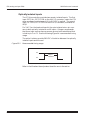
≡ Avoiding damage to the heatsink/CPU
WARNING!
When handling any Octagon CPU card, extreme care must be
taken not to strike the heatsink against another object, such
as a table edge. Also, be careful not to drop the CPU card,
since this may cause damage to the heatsink/CPU as well.
Epoxy adhesive bonds the heatsink to the CPU chip. When
the heatsink is struck, the epoxy adhesive does not allow the
heatsink to separate from the chip. The force of the blow to
the heatsink then causes the legs of the CPU chip to separate
from the PCB. This force damages both the CPU chip and
the PCB.
Note
Any physical damage to the CPU control card is not covered under
warranty.
Notice to user
PC-500 user’s manual
6000 Series user’s manual
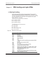
About this manual
About this manual
The 6000 Series user’s manual provides information about installing
and configuring your model in the 6000 Series of PC Microcontrollers.
This manual is divided into four sections:
n Section 1 – Installation
Chapter 1:
Overview
Chapter 2:
Quick start
Chapter 3:
Setup programs
Chapter 4:
Save and run programs
n Section 2 – Hardware
Chapter 5:
Serial ports
Chapter 6:
EZ I/O
Chapter 7:
AUX I/O
Chapter 8:
Analog I/O
Chapter 9:
SSDs, DRAM, and battery backup
Chapter 10:
External drives
Chapter 11:
Video
Chapter 12:
IRQ routing and opto IRQs
Chapter 13:
LED signaling and “beep” codes
Chapter 14:
PC/104 expansion
Chapter 15:
Counter timer controller
n Section 3 – System management
Chapter 16:
Watchdog timer, reset, and remote reset
Chapter 17:
Serial EEPROM
Chapter 18:
CPU power management
Chapter 19:
Using PICO FA
Chapter 20:
CAMBASIC
Chapter 21:
Software utilities
Chapter 22:
Troubleshooting
n Section 4 – Appendices
Appendix A:
6010 technical
Appendix B:
6020 technical
Appendix C:
6030 technical
Appendix D:
6040 technical
Appendix E:
6050 technical
Appendix F:
Miscellaneous
Appendix G:
Accessories
data
data
data
data
data
About this manual
6000 Series user’s manual
6000 Series user’s manual
Chapter 1:
Overview
Overview
≡ Introduction
The Octagon 6000 Series PC Microcontroller™ cards are intended for
easy usage and high performance in embedded control applications.
The PC Microcontroller cards combine the best features of the PC architecture and microcontroller I/O. Bringing PC software to the
microcontroller world eliminates the need to maintain development
systems for the different microcontroller chips. The Octagon PC
Microcontrollers operate in severe environments, providing an extra
margin of reliability in any application. Although ROM-DOS™ 6.22 is
included, you can download other operation systems into the flash drive.
If you prefer operating in a high-level language, CAMBASIC has been
built-in as a fast, easy-to-use, industrial control language.
Common features across the PC Microcontroller product line include:
n Suite of embedded software
— Datalight ROM-DOS™ 6.22 in ROM
— Phoenix PICO FA™ flash file system
— CAMBASIC™ multitasking language
— RS-422/485 networking software–up to 32 nodes
— Phoenix BIOS™ with industrial BIOS extensions
— Driver library
— Diagnostic software
n 40 MHz 386SX processor
n 2/4 MB of on-card DRAM
n Two solid-state disks
— 1 MB flash SSD with an integral programmer
— 128 KB SRAM SSD with battery backup
n Two serial ports with 8 KV ESD protection
n Multifunctional parallel port
n Keyboard and speaker ports
n Watchdog timer
n Real time calendar/clock (see note on page 1-7)
n Two opto-isolated interrupt inputs
n System status LEDs
n Stand alone or ISA bus expansion
n -40° to 85°C when operating at 25 MHz
0° to 60° C when operating at 40 MHz
n 10g shock, 2g vibration
1-1
Overview
6000 Series user’s manual
n 5V operation
n Low power mode
n Over voltage/reverse voltage protection
Unique features of each PC Microcontroller are listed in the following
table.
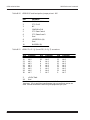
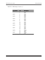
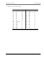
Table 1-1
Features of the PC Microcontrollers
Features
6010
6020
6030
6040
6050
COM ports
2
2
4
2
2
COM3 and COM4
—
—
RS-232
—
industrial
—
RS-232 to RS-422/485
NO
option
YES
YES
YES
YES
EZ I/O digital lines
—
48
—
24
24
LPT port
1
1
1
1
1
Total digital lines—
17
includes parallel port
65
17
41
41
High current drivers
—
—
—
—
8
Analog inputs
—
—
—
8
—
Analog outputs
—
—
—
2
—
PC/104 interface
YES
NO
NO
NO
NO
EIDE port
YES
NO
NO
NO
NO
Floppy port
YES
NO
NO
NO
NO
Counter timer
controller
NO
YES
NO
NO
NO
≡ Major features
Suite of embedded software included in SSD0 flash drive
n Phoenix BIOS and Octagon industrial extensions. The BIOS is
shadowed for fast operation.
n “Instant DOS” system. Datalight ROM-DOS 6.22 loads to high
memory on powerup allowing more lower memory for data storage
and applications programs.
1-2
6000 Series user’s manual
Overview
n PICO FA flash file system makes flash memory appear as a hard
disk to the PC Microcontroller.
n CAMBASIC, industrial control language includes drivers for all
on-card hardware.
n The network kernel allows up to 32 systems to be linked into an
RS-422/485 network.
n The utility library includes application examples in C and
CAMBASIC.
n Diagnostic software is included to test the system on powerup.
CAMBASIC
CAMBASIC supports all on-card I/O including digital, analog, timing,
interrupts, communications, and other functions. Thus, CAMBASIC
eliminates the need to write hardware drivers. You spend your time
writing the applications software rather than writing and debugging
drivers.
Diagnostic software verifies system integrity automatically
The PC Microcontroller has built-in diagnostic software that can be used
to verify on-card I/O and memory functions. On powerup, a series of
tests is performed. If a problem occurs, the failed test can be identified
by the color sequence on a bicolored LED. The test is performed automatically every time the system is reset or powered up. No monitor,
keyboard, disks, test fixtures, test equipment, or software is required.
See the LED signaling and “beep” codes chapter for a complete listing of
system tests.
DRAM memory is fast and rugged
The PC Microcontroller has surface-mounted, fast page mode DRAM
installed. The surface mounting is far more rugged than plug-in
memory.
Solid-state disks withstand shock and vibration
SSD0 is a 1 MB flash memory disk containing the software suite in less
than 512 KB, leaving more than 512 KB available for user programs.
The flash memory is seen by software as a hard disk. The use of the
flash allows easy installation of software updates.
SSD2 is an SRAM with 128 KB capacity for data storage. SSD2 is
battery-backed with an on-board battery.
1-3
Overview
6000 Series user’s manual
Boot sequence
A PC Microcontroller can be configured to boot from the on-card solidstate disk, an external floppy disk, or hard disk.
Serial ports protected against ESD
The COM1 and COM2 serial ports are 16C550 compatible. The 16 byte
FIFO buffers minimize processor overhead in high speed serial communications. Baud rates are programmable from 150 to 115 KB baud.
Both ports have an RS-232 interface with the RS-232 voltages generated on-card. The serial ports meet the new IEC1000, level 3, ESD
protection specification with ±8 KV of ESD protection. Backdrive protection is also included.
CAMBASIC supports the serial ports with interrupt driven, 2 KB input
and output buffers which operate in the background. This ensures that
data is not lost while critical control loops are being executed.
Note
The network interface module is not compatible with the 6010 model.
Convenient I/O termination with the breakout board (BOB)
Except for the serial and industrial I/O lines, all other I/O is terminated
with a 34-pin IDC connector, also called the AUX I/O. The AUX I/O
port eliminates cable clutter and the possibility of cables being plugged
into the wrong sockets during maintenance. The breakout board terminates each function at the appropriate connector. These functions
include the keyboard, speaker, printer, floppy drive, battery, and optoisolated interrupts.
Speaker and keyboard
The PC Microcontroller accepts a PS-2 style AT keyboard and provides
speaker output through the breakout board (BOB).
Parallel port is multifunctional
The multifunctional parallel port can be used as a printer port or general purpose I/O. The parallel port can also interface with a floppy disk
drive, drive alphanumeric displays and matrix keypads, or drive high
current AC and DC loads using an opto rack and opto modules.
The multifunctional parallel port applications include:
n LPT1 for PC compatible printers
n 17 general purpose digital I/O lines
n 4 x 4 matrix keypad
n 4 line alphanumeric display
1-4
6000 Series user’s manual
Overview
n MPB-16PC, 16 position opto-module rack
n Floppy disk drive
The printer port is IEEE 1284A compliant, unidirectional and bidirectional, EPP (enhanced parallel port) mode, and ECP (extended capabilities port) mode compatible. The printer port features backdrive protection and allows for much higher speed transfers than Octagon’s previous
standard printer interface. The data lines can sink up to 24 mA. The
printer port signals are routed through the PC Microcontroller’s
AUX I/O port when using the breakout board.
Keypad and LCD/VF display support for low cost operator
interface
For embedded applications, a keypad and display (KAD) board and
software are available to interface with an alphanumeric display and
matrix keypad. The parallel port on the KAD can interface with a
16-key matrix keypad and a 2 or 4 line LCD or vacuum florescent
display in applications where an inexpensive operator interface is
needed. The microcontroller cards are supplied with the software which
provides keypad scanning and display operation. The keypad and
display board has sockets for the display and keypad. DISPLAY and
KEYPAD commands in CAMBASIC and drivers in C support these
devices.
Industrial I/O is EZ I/O
Several PC Microcontrollers feature the Octagon EZ I/O digital I/O chip.
EZ I/O supplies 24 I/O lines which can be individually programmed as
5V input or 5V output. Each line can sink or source 15 mA. The 24 I/O
lines are divided into three groups of 8 with 10 K resistors that can be
connected to ground or +5V. The EZ I/O port can drive the MPB series
opto-isolation module racks directly, controlling input and loads to 240V
and 3A. CAMBASIC has several commands to support the EZ I/O port
when working on bit, BCD, byte, or word bases.
High current outputs
Model 6050 dedicates 8 lines as high current outputs, capable of driving
100 mA loads rated up to 50V.
External interrupt and reset are optically isolated for safety
One opto-isolated input causes a master reset; and the other causes the
system to generate an IRQ9. Both inputs accept voltages from 4.5 to 6
VDC. This could be used for an emergency stop, power failure, system
synchronization, or a similar function. Drivers are provided in CAMBASIC and C.
1-5
Overview
6000 Series user’s manual
Interrupts used to the maximum
Real time operation often requires many interrupts for high speed
response to events. Five of the AT interrupts are connected to the ISA
bus in addition to the four interrupts used on the card This provides the
best use of the interrupts for demanding applications.
System expansion is flexible
The PC Microcontroller can expand via an 8-bit ISA unterminated
backplane with the Octagon 5000 Series expansion cards.
Mounting
There are several ways to mount a PC Microcontroller:
n Plug it directly into an Octagon Micro PC card cage. Power is supplied through the backplane.
n Use the optional PC mounting bracket and plug it into any passive
ISA backplane. Power is supplied through the backplane.
n Panel mount it using the four mounting holes for stand alone operation. A two position terminal connector is used to supply the 5V
power.
n Stack it with other Micro PC cards. An Octagon two card stacking
kit or a flexible backplane using 3M connectors and ribbon cable can
be used to stack several cards together.
Hardware reset
A hardware reset can be done by any of the following means:
n Issuing the RESET software command, using the watchdog function
n Depressing the reset switch
n Cycling power
n Input from an optically-isolated reset.
A hardware reset ensures complete reset of the system and all attached
peripherals. An expired watchdog timer cycle also causes a hardware
reset to occur.
Watchdog timer for added safety
The watchdog timer resets the system if the program stops unexpectedly. The watchdog is enabled, disabled, and strobed under software
control. The time-out is 1.6 seconds (typical).
1-6
6000 Series user’s manual
Overview
SETUP information stored in EEPROM for high reliability
The loss of SETUP data is serious in industrial applications. In the
PC Microcontroller, SETUP data is stored in nonvolatile serial
EEPROM eliminating the problem with battery or power failure
(with the exception of time and date). 512 bytes of the serial
EEPROM are reserved by the BIOS. An additional 1536 bytes are
available to the user. A software driver is supplied for accessing the
EEPROM.
Real time calendar/clock with battery backup
The PC Microcontroller has a built-in AT style, real time clock. The
real time clock is powered by an external AT style battery. For
additional backup, an on-card battery powers the calendar/clock when
the external battery is being replaced. The clock may be read either
through DOS or CAMBASIC. The calendar/clock also provides the
user with 128 bytes of user-defined CMOS-RAM.
Note: The date and time occasionally resets to default. If your application requires date/time stamping you should consider another Octagon Systems CPU card.
Power management reduces power by more than 70%
Power management can be used to reduce power consumption or to
freeze the state of the program on the occurrence of a power management interrupt. Power consumption can be reduced by more than 70%,
reducing the heat load and extending battery life in mobile applications.
Rugged environmental operation
The CPU case temperature may range from -40° to 85°C during operation at 25 MHz, or 0° to 60° C during operation at 40 MHz. The PC
Microcontroller is designed to withstand 10g shock and 2g vibration.
5 volt only operation lowers system cost
The PC Microcontroller operates from a single 5V ± 4% supply. Located across the power supply, the 6.2V, 5W diode protects against
reverse voltage and limits over voltage. Power is supplied to the card
either through the ISA bus connector or the terminal block.
1-7
Overview
6000 Series user’s manual
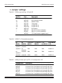
≡ Reference designators
Before you continue with the installation of your PC Microcontroller,
review the following tables for a list of connectors and jumper blocks for
the functions on your particular model in the 6000 Series of PC
Microcontrollers.
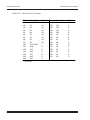
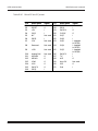
Table 1-2
1-8
6000 Series connectors
Reference
designator
6010
6020
6030
6040
6050
COM1
J3
J3
J3
J3
J3
COM2
J4
J4
J4
J4
J4
COM3
—
—
J1
—
—
COM4
—
—
J7
—
—
AUX I/O
J2
J2
J2
J2
J2
Power
J5
J5
J5
J5
J5
Battery
J6
J6
J6
J6
J6
Analog I/O
—
—
—
J7
—
USESETUP
W1
W1
W1
W1
W1
EZ I/O 1
—
J1/W3
—
J1/W2/W4
J1/W2
EZ I/O 2
—
J7/W3
—
—
—
D/A
—
—
—
W3
—
I/O range select A/
BIOS device
W2
W2
W2
W2
W2
PC/104
J1
—
—
—
—
Floppy
J8
—
—
—
—
Hard drive
J7
—
—
—
—
6000 Series user’s manual
Chapter 2:
Quick start
Quick start
This chapter covers the basics of setting up a PC Microcontroller system. The following topics are discussed:
n Panel mounting, stacking, or installing the PC Microcontroller into
an Octagon card cage
n Setting up a serial communications console I/O link between the PC
Microcontroller and your desktop PC
n Downloading files to the PC Microcontroller and running a program
from the virtual drive.
WARNING!
The PC Microcontroller may not be installed in a PC. These
cards are designed to be independent CPU cards only, not
accelerators or coprocessors.
≡ Hardware installation
WARNING!
The PC Microcontroller card contains static-sensitive CMOS
components. The card is most susceptible to damage when it
is plugged into a card cage. The PC Microcontroller becomes
charged by the user, and the static discharges to the backplane from the pin closest to the card connector. If that pin
happens to be an input pin, even TTL inputs may be damaged. To avoid damaging your card and its components:
n Ground yourself before handling the card
n Disconnect power before removing or inserting the card.
WARNING!
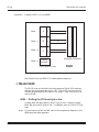
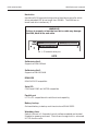
Take care to correctly position the PC Microcontroller in the
card cage. The VCC and ground signals must match those on
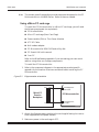
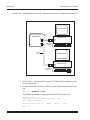
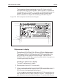
the backplane. Figure 2-1 shows the relative positions of the
PC Microcontroller as it is installed in the card cage.
Your PC Microcontroller can be installed in one of several ways:
n Plugging it directly into an 8-bit Micro PC card cage
n Using the optional PC mounting bracket and plugging it into any
8-bit passive ISA backplane
n Panel mounting it using the four mounting holes
n Stacking it with other Micro PC cards.
2-1
Quick start
6000 Series user’s manual
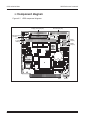
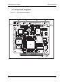
Note
The product-specific appendices provide component diagrams for the PC
Microcontrollers in the 6000 Series. Refer to them as needed.
Using a Micro PC card cage
To install the PC Microcontroller in a Micro PC card cage, you will need
the following equipment (or equivalent):
n PC Microcontroller
n Micro PC card cage (5xxx Card Cage)
n Power module (510x or 71xx Power Module)
n VTC-9F Cable
n Null modem adapter
n PC Microcontroller ROM-DOS and utility disk
n PC SmartLINK with manual
n Your PC
Refer to the Miscellaneous appendix if you are making your own serial
cable or using other non-Octagon components.
To install the PC Microcontroller:
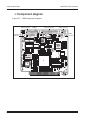
1. Refer to the component diagram in the appropriate product-specific
appendix for the location of various connectors before installing the PC
Microcontroller.
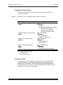
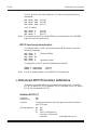
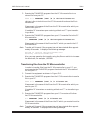
Figure 2-1
Edge connector orientation
A31
B31
Micro-PC
Passive
Backplane
Card Edge Pins
A31 & B31
PC Microcontroller
A1
B1
Card Edge Pins
A1 & B1
2. Attach the Octagon power module to the card cage following the instructions supplied with the power module.
3. Make sure power to the card cage is OFF.
2-2
6000 Series user’s manual
Quick start
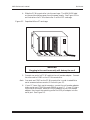
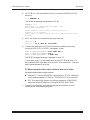
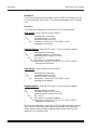
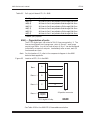
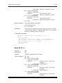
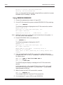
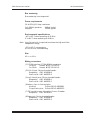
4. Slide the PC Microcontroller into the card cage. The ROM-BIOS label
on the card should face away from the power supply. See Figure 2-2 for
an illustration of a PC Microcontroller in a Micro PC card cage.
Figure 2-2
Populated Micro PC card cage
WARNING!
Plugging in the card incorrectly will destroy the card!
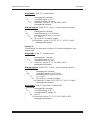
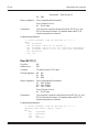
5. Connect one end of a VTC-9F cable to the null modem adapter. Connect
the other end to COM1 on the PC Microcontroller.
Note
You must use COM1 on the PC Microcontroller in order to establish a
serial communications console I/O link with your PC.
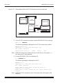
6. If your PC has a 9-pin serial connector, connect the null modem adapter
to any serial port (COM1 through COM4) on your PC. If your PC has a
25-pin serial connector, attach a 9-25 pin adapter to your null modem
adapter, then insert the matching end of the 9-25 pin adapter into the
serial port. See Figure 2-3.
2-3
Quick start
6000 Series user’s manual
Figure 2-3
Serial communications setup
DB-9
Connectors
Desktop PC
C
9F
COM1
VTC-
e
ab l
COM Port
Null Modem
Adapter
OR
PC Microcontroller
DB-9 to DB-25
Adapter
Desktop PC
9F
VTC-
bl e
Ca
Null Modem
Adapter
Note
COM Port
DB-25
Connector
Refer to the PC SmartLINK manual for more information on using a
desktop PC COM port other than COM1.
You are now ready to transfer files between your PC and the PC Microcontroller. Continue with the section, Establishing communications
with the PC Microcontroller, in this chapter.
Panel mounting or stacking the PC Microcontroller
To panel mount or stack the PC Microcontroller, you will need the
following equipment (or equivalent):
n PC Microcontroller
n 5V power supply
n VTC-9F cable
n Null modem adapter
n PC Microcontroller ROM-DOS and utility disk
n PC SmartLINK with manual
n Your PC
n 5252MB stacking kit (required for stacking only) (P/N 3590)
Refer to the Miscellaneous appendix if you are making your own serial
cable or using other non-Octagon components.
2-4
6000 Series user’s manual
Quick start
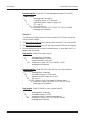
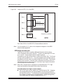
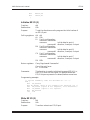
If you are panel mounting the PC Microcontroller, a screw terminal
connector is provided to supply the 5V power. Refer to Figure 2-4 for an
illustration of panel mounting the PC Microcontroller.
WARNING!
Miswiring the voltage at P2 of the PC Microcontroller or at
the power connector of the 5252MB stacking kit (reversing
+5V and ground, or applying a voltage greater than +5V), will
destroy the card and void the warranty!
Figure 2-4
Panel mounting the PC Microcontroller
Power connector
Figure 2-5
Stacking the PC Microcontroller
Power connector
5252MB
stacking kit
1. To panel mount the PC Microcontroller, use #4-40 standoffs and screws
to secure the card. The following diagram shows the center-to-center
mounting hole dimensions.
2-5
Quick start
6000 Series user’s manual
To stack the PC Microcontroller, refer to the 5252MB stacking kit product sheet enclosed with the kit. Then proceed with Step 2 in this section.
Figure 2-6
PC Microcontroller center-to-center hole dimensions
A
A = 4.90 in. (124,46 mm)
B = 0.20 in. (5,08 mm)
C = 3.50 in. (88,90 mm)
D = 0.10 in. at 45°, 2 PLCS
(2,54 mm at 45°)
E = 0.475 in. (4,44 mm)
F = 0.85 in. (21,59 mm)
J
G = 3.20 in. (81,28 mm)
H = 0.30 in. (7,62 mm)
J = 4.20 in. (106,68 mm)
K = 0.20 in. (5,08 mm)
L = 4.50 in. (114,30 mm)
M = .475 in (12,07 mm)
B
0.125 in. HOLE
(3.17 mm)
4 PLCS
L
C
0.015 in. at 45• CHAMFER, 2 PLCS
(0,038 mm)
A31
A1
M
H
F
G
K
F
E D
BEVEL CARD EDGE, 2 PLCS
.015 in. x 45• (0,038 mm x 45•)
2. Connect the ground and 5V wires to the terminal block of the PC Microcontroller or P2 of the stacking kit.
3. Connect one end of the VTC-9F cable to the null modem adapter. Connect the other end to COM1 on the PC Microcontroller.
Note
You must use COM1 on the PC Microcontroller in order to establish a
serial communications console I/O link with your PC.
4. If your PC has a 9-pin serial connector, connect the null modem adapter
to any serial port (COM1 through COM4) on your PC. If your PC has a
25-pin serial connector, attach a 9-25 pin adapter to your null modem
adapter, then insert the matching end of the 9-25 pin adapter into the
serial port. See Figure 2-3.
Note
Refer to the PC SmartLINK manual for more information on using a
desktop COM port other than COM1.
You are now ready to transfer files between your PC and the PC Microcontroller. Continue with the section, Establishing communications
with the PC Microcontroller in this chapter.
2-6
6000 Series user’s manual
Quick start
Using the PC Microcontroller in a passive ISA backplane
To plug the PC Microcontroller into a passive ISA backplane, you will
need the following equipment (or equivalent):
n PC Microcontroller
n Unterminated backplane
n Mounting bracket (optional)
n Power module
n VTC-9F cable
n Null modem adapter
n PC Microcontroller ROM-DOS and utility disk
n PC SmartLINK with manual
n Your PC
Refer to the Miscellaneous appendix if you are making your own serial
cable or using other non-Octagon components.
To install the PC Microcontroller:
1. Make sure power to the backplane is OFF.
2. Insert the PC Microcontroller into a connector on the backplane (see
Figure 2-7). Take care to correctly position the card’s edge with the
connector of the backplane. Figure 2-1 shows the relative positions of
the PC Microcontroller card as it is installed into a backplane.
WARNING!
Incorrectly plugging the card into the backplane will
destroy the card and void the warranty!
Figure 2-7
Using a passive ISA backplane
Mounting bracket
XT/AT passive backplane
2-7
Quick start
6000 Series user’s manual
3. Connect one end of a VTC-9F cable to the null modem adapter. Connect
the other end to COM1 on the PC Microcontroller.
Note
You must use COM1 on the PC Microcontroller in order to establish a
serial communications console I/O link with your PC.
4. If your PC has a 9-pin serial connector, connect the null modem adapter
to any serial port (COM1 through COM4) on your PC. If your PC has a
25-pin serial connector, attach a 9-25 pin adapter to your null modem
adapter, then insert the matching end of the 9-25 pin adapter into the
serial port. See Figure 2-3.
Note
Refer to the PC SmartLINK manual for more information on using a
desktop PC COM port other than COM1.
You are now ready to transfer files between your PC and the PC Microcontroller. Continue with the section, Establishing communications
with the PC Microcontroller in this chapter.
≡ Establishing communications with the PC
Microcontroller
1. Install PC SmartLINK (or other communications software) on your PC
if you have not already done so. Refer to the PC SmartLINK manual
for installation instructions.
2. Copy the PC Microcontroller files from the supplied utility disk to a
subdirectory on your PC hard drive.
C:
MD C:\MPC
XCOPY A:\*.* C:\MPC /S
3. Start PC SmartLINK. You are now ready to establish communications
between your PC and the PC Microcontroller.
4. Power on the PC Microcontroller.
5. A logon message similar to the one below will appear on your PC monitor:
PhoenixBIOS (TM) A386 Version x.xx
Copyright (C) 1985-1992 Phoenix Technologies, Ltd.
All Rights Reserved
Octagon Systems Corp. 40 MHz 60xx CPU
Release vx.xx - mm/dd/yy
Ali 386SX-V8T processor detected operating at 40 MHz
640K Base Memory, 1024K Extended
INT 17h BIOS extension vx.xx
Copyright (c) 1995-97 Octagon Systems Corporation
PICO Flash Array
2-8
6000 Series user’s manual
Quick start
Copyright (c) 1996,Phoenix Technologies Ltd.
Resident Flash (RFA) OEM Layer
Phoenix PICO Flash Array (TM)
Copyright (c) 1996
Phoenix Technologies LTD
Octagon Systems vx.xx
First drive of size 896K is installed in SSD0 (AMD 1MB flash)
Second drive of size 128K is installed in SSD2 (128K SRAM)
RS-485 support BIOS extension vx.xx
Copyright (c) 1996, Octagon Systems
Starting ROM-DOS...
HIMEM v6.22 (Revision x.xx)
Copyright (c) 1989-1995 Datalight, Inc.
VDISK v6.22 (Revision x.xx)
Copyright (c) 1989-1995 Datalight, Inc.
Extended Memory Present
VDISK v6.22 (Revision x.xx)
Copyright (c) 1989-1995 Datalight, Inc.
Formatting 1024K XMS memory as drive E:
60xx C:\>
If you do not get the proper logon message:
n Check the PC SmartLINK serial parameters of your PC to make sure
they are set correctly. Parameters should be 9600 baud, 8 data bits,
no parity, and 1 stop bit.
n Make sure a video card is not installed in the card cage
n Make sure all jumpers are set to factory defaults
n If the system still does not respond, refer to the Troubleshooting
chapter.
6. Use the directory command to make sure your equipment and software
are working properly. Enter:
60xx C:\> DIR
A directory listing of ROM-DOS files stored in the BIOS socket should
appear:
Volume in drive C has no label
Directory of C:\
AUTOEXEC
BAT
43
09-12-96 2:03p
COMMAND
COM 26,321
04-17-95 6:22a
CONFIG
SYS
73
09-12-96 2:03p
DOS
<DIR>
02-24-97 10:57p
UTILS
<DIR>
02-24-97 10:57p
CAMBASIC
<DIR>
02-24-97 10:57p
6 file(s)
26,437 bytes
489,472 bytes free
7. You are now ready to transfer files between your PC and the PC
Microcontroller.
2-9
Quick start
6000 Series user’s manual
≡ Transferring files between the PC Microcontroller
and your PC
Once you have established communications between your PC and the
PC Microcontroller, you can serially download files to any read/write
drive used by the PC Microcontroller. You can then test and debug your
application files. You can also upload files from the PC Microcontroller
to your desktop PC for editing and debugging.
When booting from the PC Microcontroller BIOS drive, the default
CONFIG.SYS device drivers designate drive C: as the BIOS drive
(SSD0), drive D: as the SRAM drive (SSD2), and drive E: as the virtual
drive. All drives assigned, can be accessed as read/write drives and files
can be serially transferred to and stored on any of these drives.
Note
The virtual drive is optional when booting from SSD0, floppy drive or
hard drive. If you do not need a virtual drive, do not use VDISK.SYS.
There are two methods to download files through the serial port to the
PC Microcontroller:
n The TRANSFER utility is used to download files, one at a time, to
the PC Microcontroller using the XMODEM protocol.
TRANSFER.EXE resides on the PC Microcontroller BIOS drive and
on the PC Microcontroller utility disk and is used to send or receive
files via the serial port (e.g., COM1). TRANSFER.EXE uses the
XMODEM protocol, as does PC SmartLINK. (See the note below on
XMODEM).
Note
1.
2.
3.
4.
5.
6.
7.
In Windows 95 when the TRANSFER utility is used to download files,
set the idle time sensitivity of PC SmartLINK on your desktop PC to
“low” for TRANSFER to run quickly. To change your settings, follow
the steps below:
Open Windows Explorer.
Select SL.EXE with the right mouse button.
Select the Properties menu item.
Select the Miscellaneous tab in the Properties window.
Move the Idle Sensitivity slide bar to low.
Select the Apply button.
Exit the Properties window.
n REMDISK/REMSERV utilities allow access to all of the files on a
remote disk drive. REMDISK.EXE and REMSERV.EXE are located
on the PC Microcontroller BIOS drive and the PC Microcontroller
utility disk. Once these programs are executed, single or multiple
files can then be transferred to and from the PC Microcontroller
using DOS COPY or XCOPY commands.
Note
2-10
REMDISK/REMSERV will not work with Windows 95. Use
REMDISK/REMSERV with ROM–DOS, MS–DOS, or on a network.
6000 Series user’s manual
Quick start
TRANSFER.EXE, REMDISK.EXE, and REMSERV.EXE are located on
the PC Microcontroller BIOS drive, in the DOS directory, and on the PC
Microcontroller utility disk in the \DOS directory. Refer to the Software
utilities chapter for more information on these programs.
Note
XMODEM only transfers files in which the file size is exactly on a
128 byte boundary. If the file size does not fall exactly on the boundary,
XMODEM automatically rounds the file size up to the next 128 byte
boundary with padding characters. For example, a file with a size of
10,000 bytes, will be rounded up to 10,112 bytes, transferred, and
written with the new file size. In most cases, this is not a concern, but
in some instances the XMODEM padding causes problems. The padding problems become apparent when an application program is expecting a specific file size or is expecting characters other than the padding
characters to be at the end of the file.
The following information on downloading files between the PC Microcontroller and your PC uses the example program DEMO.EXE. This file
is on the PC Microcontroller utility disk in the \DEMO directory.
Downloading files to the PC Microcontroller using
TRANSFER.EXE
The following procedures assume you are using PC SmartLINK and
that it is included in your directory path. For other communication
programs, refer to their instructions on sending a file from your PC to a
target system. Refer to the Software utilities chapter for specific information on using TRANSFER.EXE.
Hardware and software requirements:
n Desktop PC, running PC SmartLINK, connected by a VTC-9F cable
and a null modem adapter to COM1 of the PC Microcontroller
n A PC Microcontroller running TRANSFER.EXE out of COM1.
2-11
Quick start
6000 Series user’s manual
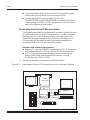
1. Connect the equipment as per the following diagram:
Figure 2-8
Downloading files using TRANSFER.EXE
PC SmartLINK
PC Microcontroller
VTC-9F
cable
COM1
TRANSFER.EXE
Desktop PC
COM port
Null modem
adapter
2. On the desktop PC, log into the directory which contains the file(s) you
will download to the PC Microcontroller, for example:
C:\MPC\60xx\DEMO
3. Start PC SmartLINK and power on the PC Microcontroller.
4. Execute the TRANSFER.EXE program from the PC Microcontroller by
entering:
60xx C:\> TRANSFER E:DEMO.EXE
Note
In this case, E: is the virtual drive assigned in CONFIG.SYS. Any PC
Microcontroller read/write drive could be substituted.
Note
When sending a file, enter the following:
60xx C:\> TRANSFER /S
The following message is displayed from the PC Microcontroller:
Receiving E:DEMO.EXE . . .
5. Execute the following steps using PC SmartLINK:
a. Press <ALT><D> to enter the download screen.
b. Type in the name of the file to transfer, e.g. DEMO.EXE (if PC
SmartLINK was not started in the DEMO directory as instructed in
Step 2, then the entire path may have to be entered
C:\MPC\DEMO\DEMO.EXE)
2-12
6000 Series user’s manual
Quick start
c. To begin the transfer, do one of the following:
n press ENTER (default download START)
n tab to START and press ENTER
n mouse click on the START button in the download screen.
d. When the file transfer is completed, press <ESC> twice to return to
the main PC SmartLINK screen.
Note
TRANSFER.EXE will time-out if the program has not been started after
approximately 40 seconds. If the time-out occurs, the following message
from the PC Microcontroller is displayed:
Failed to receive E:DEMO.EXE!
Deleting E:DEMO.EXE
6. When the file transfer is complete, type the following DOS command to
view the E: drive directory and confirm that your file has been transferred to the PC Microcontroller:
60xx C:\> DIR E:
The system will display the contents of drive E:
Volume in drive E is VDISK vX.XX
Directory of E:\
DEMO EXE
27264 06-07-96
2:57p
1 file(s) 27264 bytes
7. To execute the program you have just downloaded, type:
60xx C:\> E:DEMO
The DEMO program displays a message on your PC.
Downloading files to the PC Microcontroller using REMDISK/
REMSERV
There are three methods of using REMDISK/REMSERV with a PC
Microcontroller:
n PC Microcontroller with no video card and one serial cable
n PC Microcontroller with no video card, two PCs, and two serial cables
n PC Microcontroller with a 5420 video card and one serial cable.
Refer to the Software utilities chapter for specific information on using
REMDISK.EXE and REMSERV.EXE.
Note
REMDISK/REMSERV will not work with Windows 95 or on a network.
Use REMDISK/REMSERV with ROM–DOS or MS–DOS.
2-13
Quick start
6000 Series user’s manual
PC Microcontroller with no video card and one serial cable
Hardware and software requirements:
n Desktop PC, running C:\DOS\REMDISK, connected by a VTC-9F
cable and a null modem adapter to COM1 of the PC Microcontroller
n A PC Microcontroller running C:\DOS\REMSERV out of COM1
1. Connect the equipment and load appropriate software on each system
as per the following diagram:
Figure 2-9
Downloading files to the PC Microcontroller with no video card using
REMDISK/REMSERV
REMDISK.EXE
PC Microcontroller
REMSERV.EXE
VTC-9F
cable
COM1
Desktop PC
COM port
Null
modem
adapter
2. On the desktop PC, start PC SmartLINK from the C:\MPC\60xx\DOS
directory and power on the PC Microcontroller.
3. Execute REMSERV.EXE on the PC Microcontroller. Read/write SSD
flash drive C: is the shared drive and COM1 is the default port. Enter:
60xx C:\DOS> \REMSERV C:
The following message is displayed from the PC Microcontroller:
REMSERV v1.0
Copyright (c) 1990-1994 Datalight, Inc.
All rights reserved.
Using COM1 at 115K+ baud. Accessing Drive C:
Time-out is 9 seconds
Press <Esc> to Exit.(There may be a delay before exit
occurs)
2-14
6000 Series user’s manual
Quick start
4. Exit PC SmartLINK by pressing <ALT><X>.
5. Execute REMDISK.EXE on the PC, by entering:
C:\> REMDISK
The following message is displayed on the PC:
Remote Disk v1.0
Copyright (c) 1990-1994 Datalight, Inc.
All rights reserved.
Installed as Drive E:
Note
/COM1
/B115+
/T10
REMDISK.EXE is located in the \DOS directory on the PC Microcontroller utility disk. REMDISK assigns the remote drive as the last drive
in the system. In this case, drive E: was assigned.
6. Files are transferred to the PC Microcontroller’s read/write drives by
using the DOS COPY or XCOPY commands. Enter:
C:\> COPY C:\MPC\60xx\DEMO.EXE E:
C:\> DIR E:
C:\> E:DEMO.EXE
The DEMO program displays a message on your PC.
In this case, drive E: is the remote read/write SSD flash disk drive of the
PC Microcontroller. Files are easily copied between the drives.
7. When finished, execute:
C:\> REMDISK /U
This unloads REMDISK from the desktop PC.
8. Restart PC SmartLINK and reset the PC Microcontroller.
PC Microcontroller with no video card, two PCs, and two serial
cables
The first desktop PC is used as the terminal for the PC Microcontroller,
and the second desktop PC’s hard drive is accessed as a remote drive,
containing the files to be downloaded to the PC Microcontroller.
Hardware and software requirements:
n Desktop PC, running PC SmartLINK, connected by a VTC-9F cable
and a null modem adapter to COM1 of the PC Microcontroller
n Desktop PC, running REMSERV.EXE, connected by a VTC-9F cable
and a null modem adapter to COM2 of the PC Microcontroller
n A PC Microcontroller running REMDISK.EXE from COM2.
1. Connect the equipment and load the appropriate software on each
system as per the following diagram:
2-15
Quick start
6000 Series user’s manual
Figure 2-10
Downloading files to the PC Microcontroller with no video card and two PCs
PC SmartLINK
PC Microcontroller VTC-9F
cable
REMDISK.EXE
COM1 COM2
Desktop PC #1
COM
port
Null modem
adapter
VTC-9F
cable
REMSERV.EXE
COM
port
Desktop PC #2
Null modem
adapter
2. On PC #1 (i.e., the terminal PC), start PC SmartLINK and power on the
PC Microcontroller.
3. Execute REMDISK.EXE from COM2 on the PC Microcontroller by entering:
60xx C:\> REMDISK /COM2
The following message is displayed from the PC Microcontroller:
Remote Disk v1.0
Copyright (c) 1990-1994 Datalight, Inc.
All rights reserved.
Installed as Drive F:
60xx C:\>
2-16
/COM2
/B115+
/T10
6000 Series user’s manual
Quick start
4. On PC #2 (i.e., the remote disk drive PC), execute REMSERV.EXE by
entering:
C:\> REMSERV C:
The following message is displayed on PC #2:
REMSERV v1.0
Copyright (c) 1990-1994 Datalight, Inc.
All rights reserved.
Using COM1 at 115K+ baud. Accessing Drive C:
Time-out is 9 seconds
Press <Esc> to Exit.(There may be a delay before exit
occurs)
5. At PC #1, access the remote disk drive by entering:
60xx C:\> F:
60xx G:\> CD F:\MPC\PC 60xx\DEMO
6. Files are transferred to the PC Microcontroller read/write drives by
using the DOS COPY or XCOPY commands. Enter:
60xx F:\MPC\60xx\DEMO> COPY DEMO.EXE C:
60xx F:\MPC\60xx\DEMO> DIR C:
60xx F:\MPC\60xx\DEMO> C:DEMO.EXE
The DEMO program displays a message on your PC.
In this case, drive F: is the remote disk drive of PC #2, and drive C: is
the read/write SSD flash disk drive of the PC Microcontroller. Files are
easily copied between the drives.
PC Microcontroller with a video card and one serial cable
Hardware and software requirements:
n Desktop PC, running REMSERV, connected by a VTC-9F cable and
a null modem adapter to COM1 or COM2 of the PC Microcontroller.
n A PC Microcontroller system, including a keyboard, a 5420 SVGA
video card and VGA monitor, running REMDISK from COM1.
1. Connect the equipment and load the appropriate software on each
system as per the following diagram:
2-17
Quick start
6000 Series user’s manual
Figure 2-11
Downloading files to the PC Microcontroller with a video card
REMDISK.EXE
5420
SVGA Card
REMSERV.EXE
VTC-9F
cable
COM1
PC
Microcontroller
Desktop PC
COM
port
REMDISK.EXE
Null
modem
adapter
2. On the PC Microcontroller system, execute REMDISK.EXE by entering:
60xx C:\> REMDISK
The following message is displayed on the PC Microcontroller monitor:
Remote Disk v1.0
Copyright (c) 1990-1994 Datalight, Inc.
All rights reserved.
Installed as Drive F:
Note
/COM1
/B115+
/T10
REMDISK assigns the remote drive as the last drive in the system. In
this case, drive F: was assigned.
3. Execute REMSERV.EXE on the desktop PC:
C:\> REMSERV C:
The following message is displayed on the PC:
REMSERV v1.0
Copyright (c) 1990-1994 Datalight, Inc.
All rights reserved.
Using COM1 at 115K+ baud. Accessing Drive C:
Time-out is 9 seconds
Press <Esc> to Exit.(There may be a delay before exit
occurs)
Note
2-18
REMSERV.EXE is located in the PC Microcontroller utility disk \DOS
directory.
6000 Series user’s manual
Quick start
4. Files are transferred to the PC Microcontroller’s read/write drives by
using the DOS COPY and XCOPY commands. From the PC Microcontroller system, enter:
60xx C:\> COPY F:\MPC\60xx\DEMO.EXE C:
60xx C:\> DIR C:
60xx C:\> C:DEMO.EXE
The DEMO program displays a message on the PC Microcontroller
monitor.
In this case, drive F: is the remote PC disk drive, and C: is the
read/write SSD flash drive on the PC Microcontroller. Files are easily
copied between the drives.
5. When finished, on the PC Microcontroller system, execute:
60xx C:\> REMDISK /U
This unloads REMDISK from the PC Microcontroller.
6. On the desktop PC press <ESC> to exit REMSERV.
2-19
Quick start
2-20
6000 Series user’s manual
6000 Series user’s manual
Chapter 3:
Setup programs
Setup programs
This chapter discusses running the SETUP configuration program, the
SETSSD program, and the PMISETUP program on the PC
Microcontroller.
n SETUP — Configures devices set up by the BIOS such as serial
ports, floppy drives, etc.
n SETSSD — Configures PICO FA device order.
n PMISETUP — Configures power management options at a more
detailed level than SETUP.
≡ SETUP
SETUP can be entered in one of two ways:
n Running SETUP.COM
n Pressing the “backspace” key followed by the “S” key during BIOS
POST sequence (this occurs between the memory test and bootup).
Also, by removing the USESETUP jumper from the “S” position at W1,
you may force the setup to temporarily revert to the defaults shown in
the following table, which allows the user to reconfigure the setup.
The SETUP program defines the PC Microcontroller system parameters. It is shipped with default configuration parameters stored in the
serial EEPROM. Changes are made by running the SETUP program.
The SETUP program is stored on the SSD0 drive and on the PC
Microcontroller utility disk.
3-1
Setup programs
Table 3-1
6000 Series user’s manual
6000 Series setup parameters and defaults
SETUP parameters
Serial console for COM1
Description
Specifies that COM1 is to be
used for console if video card is
not present
Default
Enabled
COM1 console baud rate
Specifies communications rate
between PC & 60xx when no
video card is in use
9600
Power–on memory test
Extensive memory testing
performed on bootup
Enabled
Boot sequence
C: Only
Serial port A
Specifies whether the floppy
drive will be ignored as a boot
device
Specifies COM1 enable/disable
Serial port B
Specifies COM2 enable/disable
Enabled
Parallel (LPT) port
Specifies LPT port
enable/disable
Enabled
Parallel port mode
Specifies mode to use with
parallel port
Bidirectional
printer port
Parallel port address
Specifies LPT address
378h
Number of floppy drives
Specifies number of floppy drives 0
attached
Number of hard drives
Specifies number of hard drives
attached
0
SETUP entry via hotkey
Specifies <backspace><S>
hotkey enable/disable
Enabled
Power management for
DOS
Specifies power management
enable/disable
Enabled
Enabled
Time update after suspend Specifies to allow update of time Enabled
after suspend mode
3-2
Shadow video BIOS area
Specifies video BIOS shadow
enable/disable
Disabled
Shadow C8000h-CFFFFh
Shadow D0000h-D7FFFh
Shadow D8000h-DFFFFh
Shadow enable/disable
Shadow enable/disable
Shadow enable/disable
Disabled
Disabled
Disabled
6000 Series user’s manual
Setup programs
Running SETUP
1. Make sure you have established a serial communications console I/O
link between the PC Microcontroller and your PC. Refer to the Quick
start chapter for more information on establishing communications with
your PC Microcontroller.
2. Enter:
60xx C:\> SETUP
Note
You may also enter SETUP after the memory test and before the system has booted by pressing the “backspace” key followed by the “S” key.
3. The system will display the PC Microcontroller setup parameters and
available options. Select the option by pressing the space bar until the
correct information appears, then press <ENTER>. Press <ESC> twice
if you want to exit setup without saving your responses.
Note
Options having an * are default settings.
n
Serial Console on COM1:
Enabled*
Disabled
WARNING!
Disabling the serial console when there is no video card
present will stop further serial console communication with
the system after the system resets. Once disabled, you may
re-enable the serial console by running SETUP. To run
SETUP, choose one of the following methods:
n Remove the USESETUP jumper, reboot, and run SETUP
n Install a video card/monitor, reboot, and run SETUP.
(This method disables the serial console.)
n
COM1 Console Baud Rate:
1200
2400
4800
9600*
14400
19200
28800
38400
57600
115200
n
Power on memory test:
Enabled*
Disabled
You may want to disable the memory test to speed up the boot process.
You may also press the space bar to cancel the memory test while in
progress.
3-3
Setup programs
Note
6000 Series user’s manual
n
Boot Sequence:
C: Only*
A: Then C:
n
Serial Port A:
Enabled*
Disabled
n
Serial Port B:
Enabled*
Disabled
n
Parallel (LPT) Port:
Enabled*
Disabled
n
Parallel Port Mode:
Bidirectional mode*
EPP mode
ECP mode
Floppy disk mode
Standard (Unidirectional) mode
n
Parallel Port Address:
378h*
278h
3BCh
Standard mode is provided for compatibility only. We recommend the
use of bidirectional mode. EPP and ECP modes are provided for equipment that has the capability to operate at these modes for enhanced
performance.
n
Number of floppy drives:
0*, 1, 2
n
Onboard floppy controller: (6010 only)
Enabled
Disabled*
Floppy drive 1 size:
5.25", 360KB
5.25", 1.2 MB
3.5", 720KB
3.5", 1.44 MB*
n
3-4
n
Floppy drive 2 size:
5.25", 360KB
5.25", 1.2 MB
3.5", 720KB
3.5", 1.44 MB*
n
Number of hard drives:
0*
1
2
6000 Series user’s manual
Note
Table 3-2
Note
If you are using a 5800A or a 5815 with the PC Microcontroller, set
“Number of hard drives” to “0” on either the 5800A or 5815 or on the PC
Microcontroller. See the following table for details.
Hard drive setup
No. of drives in
HDSETUP
(5800A/5815)
1 or 2
IRQ setting in
HDSETUP
IRQ14
No. of drives in CPU
SETUP
0
0
N/A
1 or 2
The PC Microcontroller does not support floppy drives on the 5800A
without first making some modifications to the 5800A. Call Technical
Support for assistance.
n
Note
Setup programs
Onboard IDE interface: (6010 only)
Enabled
Disabled*
The 6010 has an on-board floppy controller and IDE controller. If an
external controller is desirable, the on-board controllers can be disabled
through SETUP.
n
Auto Drive Configuration
Enabled*
Disabled
n
Drive 0 parameters
Cylinders (xxx):
Heads (x):
Sectors (xx):
n
Setup entry via hotkey
Enabled*
Disabled
n
Power management
Enabled*
Disabled
n
Time update after suspend
Enabled*
Disabled
n
Shadow C8000H - CFFFFH
Disabled*
Enabled
n
Shadow D0000H - D7FFFH
Disabled*
Enabled
n
Shadow D8000H - DFFFFH
Disabled*
Enabled
3-5
Setup programs
6000 Series user’s manual
Press ENTER to SAVE the changes or
Press ESC to EXIT without saving the changes.
Saving options.
Options saved.
Depending on the options you have selected, the system may display the
following message:
You must reset for these options to take effect.
If you entered SETUP with the hotkeys (i.e., “backspace” and “S” keys),
the system will reboot automatically.
SETUP example
The following example configures a system with no memory test, 9600
baud, and booting from C:
OCTAGON SYSTEMS CORPORATION
60xx SETUP UTILITY Vx.x
(c) Phoenix Technologies, Ltd. 1985, 1995
_____________________________________________________________
(Press SPACE to CHANGE, ENTER to ACCEPT, ESC to EXIT)
Serial Console on COM1:
COM1 Console Baud Rate:
Power on memory test:
Boot Sequence:
Parallel (LPT) Port:
Parallel Port Mode:
Number of floppy drives:
Floppy drive 1 size
Number of hard drives
Auto Drive Configuration:
SETUP Entry via Hotkey:
Power Management:
Shadow Video BIOS Area:
Shadow C8000h-CFFFFh:
Shadow D0000h-D7FFFh:
Shadow D8000h-DFFFFh:
ENABLED
9600
DISABLED
C: ONLY
ENABLED
Bidirectional Printer Port
1
3.5", 1.44 MB
1
ENABLED
ENABLED
DISABLED
DISABLED
DISABLED
DISABLED
DISABLED
Press ENTER to SAVE the changes or
Press ESC to EXIT without saving the changes.
Options Saved.
You must reset for these options to take effect.
60xx C:\>
3-6
Note
Executing SETUP /D will change all setup parameters to default values.
Note
Power management should be disabled when using CAMBASIC.
6000 Series user’s manual
Setup programs
≡ SETSSD
SETSSD allows the user to set or change the PICO FA drive (SSD)
order. PICO FA drives are “simulated” hard drives. They can exist
before or after any IDE drives and can appear in any order. By setting
the order, the SSDs may be accessed as C:, D:, etc. For example,
n To set SSD0 first and SSD2 second, enter the following command:
60xx C:\> SETSSD SSD0 SSD2
If there are other hard drives on the system, add the /before option to
place the order of the SSDs before the hard drives, or add the /after
option to place the SSDs after the hard drives. For example,
n To set SSD0 as the first drive, SSD2 as the second drive, and an IDE
drive as the third drive, enter the following command:
60xx C:\> SETSSD SSD0 SSD2 /before
n To set the IDE drive as first in order and SSD0 as second, enter the
following command:
C:\> SETSSD SSD0 /after
In the last example, the IDE drive is C:, SSD2 is D: and SSD0 is E:.
Other drive letter designations may be added by device drivers (such as
VDISK.SYS), which are in the CONFIG.SYS file on the boot drive.
The boot drive is based upon the drive order set by the SETSSD command and by SETUP’s “boot sequence” option. If the boot sequence is
set to “A: THEN C:,” the system will look for a floppy disk in drive A:. If
a diskette is not installed, or a floppy is not defined, the boot drive will
be the first drive specified in the SETSSD command. If the boot sequence is set to “C: ONLY,” the check for a disk is bypassed.
Note
The SETSSD parameters may also be overwritten by removing the
USESETUP jumper from the “S” position at W1 and resetting the
system. If the parameters specified at the PICO FA first/second drive
prompt are different from the previous SETSSD command, and you
answered “No” to the “Save” prompt, the SETSSD output will not be
accurate. Therefore, we recommend that you answer “Yes” to the save
option to prevent confusion.
Note
After you run SETSSD and the drive order has changed, the new
parameters will take effect after a reset.
Note
The drive order affects the number entered at the PFORMAT Hn
command.
3-7
Setup programs
6000 Series user’s manual
≡ PMISETUP
PMISETUP allows the user to customize the power management features of the PC Microcontroller. Refer to the CPU power management
chapter. See also the Software utilities chapter for details.
3-8
6000 Series user’s manual
Chapter 4:
Save and run programs
Save and run programs
≡ Save and run your programs on the PC
Microcontroller
Once you have written, tested, and debugged your application, you can
then save it to flash memory in SSD0. When you reboot the PC
Microcontroller, your program can automatically load into DOS memory
and execute. As shipped from the factory, SSD0 already contains a
bootable ROM-DOS.
This chapter describes the following:
n Saving an application program to SSD0
n Autoexecuting the program from the PC Microcontroller
n Overriding autoexecution of your program.
The information in this chapter assumes you will be using ROM-DOS in
your application. Some Microsoft programs make undocumented DOS
calls. With ROM-DOS, an error will be returned when an undocumented
DOS call is made, causing your program to operate erratically. We
recommend booting from SSD0 and using your own DOS, when using
programs with undocumented DOS calls. Refer to the Adding operating
system startup files section in this chapter for more information on
saving and autoexecuting programs.
This chapter also assumes you will be using the PC Microcontroller
without a video card/monitor. If you are using these devices, refer to
the Video chapter for more information on transferring and saving
programs.
≡ Saving program and support files
By default, SSD0 comes from the factory preformatted, loaded with
Datalight’s ROM-DOS startup files and with an example demo program. To replace the demo program on SSD0 with your own, see Adding your application section in this chapter.
Formatting SSD0
This section describes how to format SSD0.
1. Define the SSD order with the SETSSD command. Since the command
input varies depending upon the parameters you would need to enter,
see the SETSSD command in the Software utilities chapter.
4-1
Save and run programs
6000 Series user’s manual
2. To begin formatting SSD0, execute PFORMAT as follows:
60xx C:\> PFORMAT Hn
where n is the hard drive sequence number. This number includes IDE
drives and SSDs.
For example, if you have 0 IDE drives and SETSSD shows:
[hdd] SSD0 SSD2
then enter:
60xx C:\> PFORMAT H0
On the other hand, if you have 1 IDE drive, enter:
60xx C:\> PFORMAT H1
Note
If the drive has not been previously formatted, reset the system before
accessing the drive. This allows DOS to recognize the drive and add a
letter designation to it.
Note
PFORMAT.EXE must be downloaded from the PC Microcontroller
utility disk. This file is located in the \UTILS directory.
After formatting the drive and resetting the system, you may access it
as a normal DOS drive.
Adding operating system startup files (using SYS)
To add the system files, issue the following operating systems command:
C:\> SYS x:
where x: specifies the drive letter.
For example, if your system has 1 IDE drive, and SETSSD shows “[hdd]
SSD0 SSD2,” then SSD0 should be drive D:. To SYS this drive, use the
“SYS D:” command.
4-2
Note
If you are adding the ROM-DOS operating system, SYS.COM must be
downloaded from the PC Microcontroller utility disk. This file is located
in the \DOS directory.
Note
If you are adding the MS-DOS operating system, you must first boot
from an MS-DOS bootable device (floppy or hard drive).
Note
If you are not booting from ROM-DOS, and wish to SYS ROM-DOS back
to the drive, the SYS command requires the access of the following
ROM-DOS files: COMMAND.COM, ROM-DOS.SYS and SYS.COM.
6000 Series user’s manual
Save and run programs
Adding your application
To add your application to your SSD, do the following:
1. Three methods of copying your application to the SSD are available. Do
one of the following:
a. From a local drive to the PC Microcontroller, issue the COPY
command.
b. From a host drive, download your application by issuing the
TRANSFER command when using PC SmartLINK. Refer to the
section, Transferring files between the PC Microcontroller and your
PC in the Quick start chapter.
c. To establish a remote drive and copy from it, issue the REMDISK
and REMSERV commands. Refer to the section, Transferring files
between the PC Microcontroller and your PC in the Quick start
chapter.
2. Add or remove any device drivers from your application. Remember to
add these drivers to your drive as well.
3. To autoexecute your application, add your application name to the
AUTOEXEC.BAT file. This method is the same in any DOS environment.
For instructions on downloading files using TRANSFER, REMDISK,
REMSERV, and PC SmartLINK, see the sections Transferring files
between the PC Microcontroller and your PC and Downloading files from
the PC Microcontroller in the Quick start chapter. In addition, the
Software utilities chapter provides usage instructions for REMDISK,
REMSERV, and TRANSFER.
Autoexecuting your application
This section describes how to autoexecute your application.
1. To autoexecute your application in SSD0, use the SETSSD command to
define your SSD as the boot device. Since you need to define the order
of SSD0 as the first of the SSDs (and before any IDE drives), enter the
following command:
60xx C:\> SETSSD SSD0 SSD2 /before
2. Reset the system. SSD0 is now drive C: and your application should
begin execution.
Note
If the SETUP option “Boot Sequence” is set to “A: THEN C:”, remove
any floppy in drive A: before resetting the system.
Note
The SETSSD options are not used when USESETUP (“S” position at
W1) is not jumpered.
4-3
Save and run programs
6000 Series user’s manual
Overriding the autoexecution of your application
1. Remove the jumper from the “S” position at W1 (USESETUP).
2. Reset the system. This will force the system to ignore all SETUP information, including the floppy/hard drive and the SETSSD information.
3. At the prompt, “PICO FA first drive (0=SSD0, 2=SSD2,
other=no drive),” enter “0”.
4. At the prompt, “PICO FA second drive (2=SSD2, other=no
drive),” enter “2”.
5. At the prompt, “Do you wish to save this information now?
(Y/N),” enter “Y”.
6. After saving this information, reinstall the USESETUP jumper.
7. Reset the system. The system should boot from SSD0.
4-4
6000 Series user’s manual
Chapter 5:
Serial ports
Serial ports
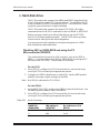
≡ Description
Each PC Microcontroller in the 6000 Series has two serial ports, except
for the 6030 which has 4 serial ports. These serial ports are 16C550
compatible. They can be used for interfacing to a printer, terminal, or
other serial device. These ports support 5-, 6- 7-, or 8-bit word lengths,
1, 1.5, or 2 stop bits, and baud rates up to 115.2 KB.
The serial ports meet IEC1000, level 3, ESD protection specification
with ±8 KV of ESD protection. Backdrive protection is also included.
COM2 can be converted to optically isolated, RS-422/485 with the
network interface module (NIM). NIM mounts directly onto the PC
Microcontroller without the need of a cable or external power supply.
Note
The Network Interface Module (NIM) is not compatible with the 6010
PC Microcontroller.
Use a VTC-9F cable to connect the ports to external serial equipment.
The pinout of the connector allows you to plug the cable directly into a
9-pin PC serial connector (refer to the product-specific appendix for the
connector pinout). When interfacing the PC Microcontroller to your PC,
you will need to use a null modem adapter. The serial port at COM1
defaults to IRQ4 at I/O address 3F8H, which is the PC standard for
COM1. Likewise, the serial port at COM2 defaults to IRQ3 at I/O
address 2F8H. Refer to Table 5-1 for the connector designation of each
COM port on your model in the 6000 Series.
Table 5-1
Serial port connector reference
Reference designator
6010
6020
6030
6040
6050
COM1
J3
J3
J3
J3
J3
COM2
J4
J4
J4
J4
J4
COM3
—
—
J1
—
—
COM4
—
—
J7
—
—
≡ Selecting console devices
The PC Microcontroller has two options for console devices:
1. Serial console from COM1, as selected with the SETUP program (“Serial
Console on COM1: ENABLED”). A serial cable/null modem adapter
plugged into a host PC running PC SmartLINK provides both input and
output. The local keyboard allows input.
5-1
Serial ports
6000 Series user’s manual
2. No console device (as selected with the SETUP program – “Serial
Console on COM1: DISABLED”) means no console output. The local
keyboard allows input.
≡ COM1 as RS-232 I/O
When you have completed developing your application and programmed
the PC Microcontroller, you can use COM1 as a standard RS-232 serial
port for connection to a printer, modem, or other serial device. COM1 as
a standard RS-232 serial port is configured at port address 3F8H. To
access COM1 as standard RS-232, configure your serial port for your
application or add a video card and monitor to your PC Microcontroller
system. Use COM1CON.EXE to return to the serial port for console
operation. Refer to the COM1CON.EXE support command in the Software utilities appendix.
Use a VTC-9F cable to connect the ports to external serial equipment.
The pinout of the connector allows you to plug the cable directly into a
9-pin PC serial connector.
≡ Using QuickBASIC to communicate via COM1
Several programming languages including QuickBASIC assume a video
card is present, and for system speed reasons write directly to the video
hardware. Assuming that a video card is present can be a problem since
many control applications require video output. The following discussion is directed at QuickBASIC, but the principles (not accessing the
print routines which access the video memory directly) apply to many
languages. There are several ways to use COM1 from QuickBASIC.
Systems with a video card
Add a video card to the system and open/close COM1 using the
QuickBASIC OPEN/CLOSE commands.
Systems without a video card
WARNING!
The system will lock up if you use commands such as PRINT
or PRINT USING. Because QuickBASIC writes directly to
video memory, these commands are usually displayed on a
monitor.
5-2
6000 Series user’s manual
Serial ports
Method 1
The system display will not appear over COM1 while the BIOS boots.
1. Run SETUP to disable the “COM1 as console” option.
2. Use QuickBASIC’s OPEN/CLOSE/PRINT/INPUT commands to access
COM1. The following is an example program using these commands:
OPEN "COM1:9600,N,8,1,BIN" FOR RANDOM AS #1
CRLF$=CHR$(13)+CHR$(10)
PRINT #1, "INPUT A STRING" + CRLF$
INPUT #1, A$
PRINT #1, CRLF$ + A$
CLOSE #1
Note
All PRINT/PRINT USING/INPUT . . . commands must use the COMx
device number, where x represents the COM port used.
Method 2
1. Run SETUP to enable the “COM1 as console” option.
2. Use QuickBASIC’s OPEN/CLOSE/PRINT/INPUT commands to access
COM1. After closing the device, manually restore the serial parameters. The following example assumes 9600, N, 8, and 1 parameters:
OPEN"COM1:9600,N,8,1,BIN" FOR RANDOM AS #1
CRLF$ = CHR$(13) + CHR$(10)
PRINT #1, "INPUT A STRING" + CRLF$
INPUT #1, A$
PRINT #1, CRLF$ + A$
CLOSE #1
Note
All PRINT/PRINT USING/INPUT . . . commands must use the COM1
device number.
3. Restore the serial parameters by using a batch file specifying your
program’s name as the first line of the file and COM1CON as the last
line of the file.
For example, TEST.BAT may include the following to execute a user
application named USECOM1:
USECOM1
COM1CON
Execute TEST.BAT.
COM1 will be used as a communication port by USECOM1, then COM1
is restored to a console port by COM1CON.
Note
COM1CON is located on the PC Microcontroller utility disk.
5-3
Serial ports
6000 Series user’s manual
Method 3
1. Run SETUP to enable the “COM1 as console” option.
2. Use the PRINTS, PRINTSL, KEYHIT$, INKEY2$ commands as found
in the DEMO.BAS and DSQBTEST.BAS programs (included on the PC
Microcontroller utility disk). Unformatted string output and string
input must be done manually.
Note
Programs written in this manner will also work with a video card
present and therefore systems can be “debugged” on your PC.
Method 4
1. Use an off-the-shelf communications library.
2. This may require restoring the COM1 parameters similar to Method 2,
if the console video is expected after the QuickBASIC program terminates.
Method 5
1. Use COM2 instead of COM1. This is similar to Method 1, but you will
still get the system displays over COM1.
Using Turbo C
If you need to restore the serial parameters after executing a C program, refer to the file COMTEST.CPP. This file can be downloaded
from the Octagon Bulletin Board at (303) 427-5368 using 14400 baud, 8
data bits, no parity, and 1 stop bit.
≡ COM2
Operation
There are two modes of operations for COM2:
n PC mode
n Network mode
The “N” position at W1 distinguishes the COM2 mode on powerup. PC
mode (“N” position at W1 jumpered, default) configures COM2 as a
standard RS-232 port. Network mode (“N” position at W1 not
jumpered) configures COM2 to communicate at 38.4 KB, respond to
Optomux type commands, respond to Octagon commands, and
automatically perform network housekeeping functions.
5-4
6000 Series user’s manual
Serial ports
PC mode/network mode
On powerup, the BIOS extension reads the “N” position at W1 to determine which COM2 mode to select.
Table 5-2
COM2 mode select
“N” position at W1
Mode
Description
Jumpered
PC mode
Use default configuration for
COM2 of 2400 baud, 8 data bits,
1 stop bit, and no parity.
Not jumpered
Network mode
Install IRQ3 vector.
Change default baud rate to
38.4 KB.
Read serial EEPROM bytes
120h,121h to determine if an ID
has been previously established.
If it has, use the existing ID, if
not, use FFh.
Discard messages addressed to
other nodes. Selectively respond
to messages addressed to node.
Await INT 17H BIOS calls to
collect messages.
COM2 as RS-232 I/O
COM2 is a standard RS-232 serial port, default configured at port
address 2F8H.
The “N” position at W1 distinguishes the COM2 mode on powerup. PC
mode (“N” position at W1 jumpered, default) configures COM2 as a
standard RS-232 port.
COM2 as RS-422/485
The PC Microcontrollers feature a predefined, easy-to-use software
interface for using COM2 as an RS-422/485 port. This software interface supports Optomux type message-passing as well as additional
Octagon messages. Up to 32 nodes are supported at a default baud rate
of 38.4 KB. This built-in feature provides a simple, low cost, and effective method of rapidly implementing an RS-422/485 network. An Octagon network interface module and an opto-isolated RS-232 to
RS-422/485 converter (Octagon P/N 4820), is required to convert RS-232
signals to RS-422/485.
Network mode (“N” position at W1 not jumpered) configures COM2 to
communicate at 38.4 KB, respond to Optomux type commands, respond
to Octagon commands and automatically perform network housekeeping
functions.
5-5
Serial ports
6000 Series user’s manual
Up to 32 nodes with valid ID range from 0 to FF are supported. ID 0 is
reserved for the host. ID FF is reserved for a new node that connects to
the network and has not yet been assigned an ID.
Both input and output ring buffer size is 2 KB.
Host/remotes
An application may implement a node as either the “host” node or as a
“remote” node in an RS-422/485 network. There can be up to 32 nodes
without any bus repeaters in the network. A “host” is referred to as the
node that initiates a communication; while a “remote” is referred to as a
node that is addressed by the host.
The host is responsible for initiating communication, maintaining
network registration, and providing housekeeping tasks with other
nodes. There can only be one network host.
Remotes cannot initiate a communication. They can only respond to
messages that are addressed to them from the host.
While there can be many remotes, all remotes initially respond to FFh
as the ID before the ID is assigned or recognized by the host. To avoid
conflict, only one new node at a time shall be added to the network.
Other unregistered nodes must not be powered up while the new node is
being registered. This allows assigning each node a unique node ID.
Once a node has been added to the network and its ID stored in serial
EEPROM, any node can thereafter attach to the network in any
powerup sequence. Periodically, the host shall try to communicate to all
the existing nodes in the network, plus the potential new node with the
ID FFh.
Network interface module (NIM)
The Octagon network interface module (NIM) is designed for easy
installation onto COM2 of the PC Microcontrollers. The NIM supports
four-wire RS-422 and two-wire RS-485 configurations. Power is supplied to the NIM via the COM2 connector on the PC Microcontroller.
For more information about the network interface module, see the NIM
product sheet.
Note
5-6
The network interface module is not compatible with the 6010 model.
6000 Series user’s manual
Figure 5-1
Serial ports
Network interface module RS-485 two-wire example
Host Transmit/
Receive Pair
NIM
COM2
PC Microcontroller
Host
NIM
COM2
PC Microcontroller
Remote
Figure 5-2
NIM
COM2
PC Microcontroller
Remote
NIM
COM2
PC Microcontroller
Remote
Network interface module RS-422 four-wire example
Host Transmit
Pair
NIM
COM2
Host Receive
Pair
PC Microcontroller
Host
Remote
Receive
Pair
NIM
COM2
NIM
COM2
NIM
COM2
PC Microcontroller
Remote
PC Microcontroller
Remote
PC Microcontroller
Remote
Remote Transmit
Pair
Refer to Octagon application notes AN-0047, AN-0048, and AN-0049 for
additional information in setting up an RS-485 network. Contact
Octagon Systems Technical Support , Customer Service, or Octagon’s
web site at www.octagonsystems.com for this information.
RS-422/485 support functions
This section provides definitions for the following INT 17h BIOS routine
functions pertinent to RS-422/485 support functions.
n Initialization
n Send message
n Receive message
5-7
Serial ports
6000 Series user’s manual
n
n
n
n
n
n
n
n
n
n
n
Get receiver status
Get transmitter status
Get ID
Set ID
Get incoming message buffer pointer
Get outgoing message buffer pointer
Set incoming message buffer pointer
Set outgoing message buffer pointer
Set roll call response
Set state wish response
Set internal state response
Function 00 – Initialization
On entry:
On exit:
AH = 0FAh
AL = 00h
DX = 0ffffh
AL = status
= RS-485 function signature
= RS-485 sub-function
= 0 -> ok
= Not 0 -> error
Function 01 – Send message
On entry:
On exit:
AH = 0FAh = RS-485 function signature
AL = 01h
= RS-485 sub-function
DX = 0ffffh
ES:BX = Transmit buffer pointer
AL = status = 0 -> ok
= Not 0 -> error
Function 02 – Receive message
On entry:
On exit:
AH = 0FAh = RS-485 function signature
AL = 02h
= RS-485 sub-function
DX = 0ffffh
ES:BX = Receive buffer pointer
AL = status = 0 -> message available
= Not 0 -> message not collected yet
Function 05 – Get receiver status
On entry:
On exit:
5-8
AH = 0FAh = RS-485 function signature
AL = 05h
= RS-485 sub-function
DX = 0ffffh
AX = incoming message status
BX = incoming message count
6000 Series user’s manual
Serial ports
Function 06 – Get transmitter status
On entry:
On exit:
AH = 0FAh = RS-485 function signature
AL = 06h
= RS-485 sub-function
DX = 0ffffh
AX = outgoing message status
BX = outgoing message count
Function 07 – Get ID
On entry:
On exit:
AH = 0FAh = RS-485 function signature
AL = 07h
= RS-485 sub-function
DX = 0ffffh
AX = our current ID
Function 08 – Set ID
On entry:
On exit:
AH = 0FAh = RS-485 function signature
AL = 08h
= RS-485 sub-function
BX = desirable ID
DX = 0ffffh
AL = status = 0 -> ok
=Not 0 -> error
Function 09 – Get incoming message buffer pointer
On entry:
On exit:
AH = 0FAh = RS-485 function signature
AL = 09h
= RS-485 sub-function
DX = 0ffffh
ES:BX = incoming message buffer pointer
Function 0a – Get outgoing message buffer pointer
On entry:
On exit:
AH = 0FAh = RS-485 function signature
AL = 0Ah
= RS-485 sub-function
DX = 0ffffh
ES:BX = outgoing message buffer pointer
Function 0b – Set incoming message buffer pointer
On entry:
On exit:
AH = 0FAh = RS-485 function signature
AL = 0Bh
= RS-485 sub-function
DX = 0ffffh
ES:BX = incoming message buffer pointer
AL = status = 0 -> ok
= Not -> error
5-9
Serial ports
6000 Series user’s manual
Function 0c – Set outgoing message buffer pointer
On entry:
On exit:
AH = 0FAh = RS-485 function signature
AL = 0Ch
= RS-485 sub-function
DX = 0ffffh
ES:BX = outgoing message buffer pointer
AL = status = 0 -> ok
= Not -> error
Function 0d – Set roll call response
On entry:
On exit:
AH = 0FAh = RS-485 function signature
AL = 0Dh
= RS-485 sub-function
DX = 0ffffh
BX = roll call response code
(See roll call reply message format)
AL = status = 0 -> ok
= Not -> error
Function 0e – Set state wish response
On entry:
On exit:
AH = 0FAh = RS-485 function signature
AL = 0Eh
= RS-485 sub-function
DX = 0ffffh
BX = state wish response code
(See state wish reply message format)
AL = status = 0 -> ok
= Not -> error
Function 0f – Set internal state response
On entry:
On exit:
5-10
AH = 0FAh = RS-485 function signature
AL = 0Fh
= RS-485 sub-function
DX = 0ffffh
BX = internal state response code
(See internal state reply message format)
AL = status = 0 -> ok
= Not -> error
6000 Series user’s manual
Serial ports
Octagon’s command set
This section provides definitions for the following Octagon RS-485
network commands:
Table 5-3
Definitions list for Octagon RS-485 network commands
From host
From remote
Roll Call (Are you there?)
>zzA**.
Reply to Roll Call
>00Zxxyy**.
xx=my ID
yy=status=00->doing fine, no request
=01->ask for ID request
=02->tell me to disconnect
=03->ask for internal state
State Wish (What ID do you want?)
>zzB**.
Reply to State Wish
>00Yxxzz**.
xx=my existing ID
zz=new ID I want to be
Assign ID (Your new ID is xx.)
>zzCnn**.
Reply to Assign ID
>00Xxxzz**.
xx=my existing ID
zz=my new ID
Report State (Report internal
state.)
>zzD**.
Reply to Report State
>00Wxxyy**.
xx=my ID
yy=user defined state response
> = start character
zz = intended listener’s ID field
** = checksum field
. = end message character
Checksum field
The checksum field of Octagon’s command set is computed by adding
the ID field to the original Optomux type checksum. Note that by
providing the checksum in this way, Optomux type equipment treats
Octagon’s add-on commands as invalid messages while Octagon’s equipment gains a unique set of commands.
5-11
Serial ports
6000 Series user’s manual
Examples
Full C code examples are included in the \EXAMPLES directory on the
PC Microcontroller utility disk. The following examples are for concept
only.
Example 1:
The following is a description of how Roll Call is implemented:
Host sends: (Dear node #1, are you there?)
>01AA3.
;>
;message start character
; 01
;intended listener is ID 01
;
A
;command code A (roll call)
;
A3
;checksum = uchar (‘0’+‘1’+’A’+0x01) = 0xA3
;
. ;message end character
Remote replies: (Dear 00: 01 is here. I have no special request.)
>00Z01007B.
;>
;message start character
; 00
;intended listener is ID 00 (host)
; Z
;command code Z (reply to roll call)
;
01
;01 = my ID
;
00 ;00 = status = no special request
;
7B;checksum = uchar (‘0’+‘0’+’Z’ +‘0’+’1’ +‘0’+’0’) = 0x7B
;
.;message end character
Host sends: (Dear node #2, are you there?)
>02AA5.
;>
;message start character
; 02
;intended listener is ID 02
;
A
;command code A (roll call)
;
A5
;checksum = uchar (‘0’+‘2’+’A’+0x02) = 0xA5
;
. ;message end character
Remote replies: (Dear 00: 02 is here. I have no special request.)
>00Z02007C.
;>
;message start character
; 00
;intended listener is ID 00 (host)
; Z
;command code Z (reply to roll call)
;
02
;02 = my ID
;
00 ;00 = status = no special request
;
7C;checksum = uchar (‘0’+‘0’+’Z’ +‘0’+’2’ +‘0’+’0’) = 0x7C
;
.;message end character
The host continues with the roll call until all nodes have been queried.
Not all of the 32 possible nodes need to be queried, only the known
nodes. When the last known node has been queried, then the host
queries for an unknown node.
5-12
6000 Series user’s manual
Serial ports
Host sends: (Dear FF, are you there?)
>FFACC.
;>
;message start character
; FF
;intended listener is ID FF
;
A
;command code A (roll call)
;
CC ;checksum = uchar (‘F’+‘F’+’A’+0xff) = 0xCC
;
. ;message end character
Remote replies: (Dear 00: FF is here. I have no special request.)
>00ZFF00A6.
;>
;message start character
; 00
;intended listener is ID 00 (host)
; Z
;command code Z (reply to roll call)
;
FF
;FF = my ID
;
00 ;00 = status = no special request
;
A6;checksum = uchar (‘0’+‘0’+’Z’ +‘F’+’F’ +‘0’+’0’) = 0xA6
;
.;message end character
Example 2:
The following is a description of how an ID can be assigned to a new
remote node:
Host sends: (Dear FF: are you there?)
>FFACC.
;>
;message start character
; FF
;intended listener is ID FF
;
A
;command code A (roll call)
;
CC ;checksum = uchar (‘F’+’F’+’A’+0xff) = 0xCC
;
. ;message end character
Remote replies: (Dear 00: FF is here. I have no special request.)
>00ZFF00A6.
;>
;message start character
; 00
;intended listener is ID 00 (host)
;
Z
;command code Z (reply to roll call)
;
FF
;FF = my ID
;
00
;00 = status = no special request
;
A6 ;checksum = uchar (‘0’+’0’+’Z’+’F’+’F’+’0’+’0’) = 0xA6
;
. ;message end character
Host sends: (Dear FF: your new ID shall be 05.)
>FFC0533.
;>
;message start character
; FF
;intended listener is ID FF
;
C
;command code C (assign ID)
;
05 ;new ID
;
33 ;checksum = uchar (‘F’+’F’+’C’+’0’+’5’+0xff)= 0x33
;
.;message end character
5-13
Serial ports
6000 Series user’s manual
Remote replies: (Dear 00: FF acknowledges my new ID to be 05.)
>00XFF05A9.
;>
;message start character
; 00
;intended listener is ID 00 (host)
;
X
;command code X (reply to assign ID)
;
FF
;FF = my ID
;
05 ;05 = my new ID
;
A9 ;checksum = uchar (‘0’+’0’+’X’+’F’+’F’+’0’+’5’) = 0xA9
;
. ;message end character
Example 3:
The following is a description of how a remote (of ID 02) can notify the
host of a state change:
1. The application program sets internal state using INT 17h function 0fh.
2. The application program sets roll call reply status to 03 (ask for Report).
3. Since a remote cannot initiate a communication, it must wait until it is
spoken to at this point.
Host sends: (Dear 02: are you there?)
>02AA5.
;>
;message start character
; 02
;intended listener is ID 02
;
A
;command code A (roll call)
;
A5 ;checksum = uchar (‘0’+’2’+’A’+0x02) = 0xA5
;
. ;message end character
Remote replies: (Dear 00: 02 is here. Ask for my internal state.)
>00Z02031F.
;>
;message start character
; 00
;intended listener is ID 00 (host)
;
Z
;command code Z (reply to roll call)
;
02
;02 = my ID
;
03 ;03 = status = Ask for a report of internal state
;
1F;checksum = uchar (‘0’+’0’+’Z’+’0’+’2’+’0’+’3’) = 0x1F
;
.;message end character
Host sends: (Dear 02: What is your internal state?)
>02DA8.
;>
;message start character
; 02
;intended listener is ID 02
;
D
;command code D (Internal state query)
;
A8
;checksum = uchar (‘0’+’2’+’D’+0x02) = 0xA8
;
. ;message end character
5-14
6000 Series user’s manual
Serial ports
Remote replies: (Dear 00: 02 internal state = 47.)
>00W024784.
;>
;message start character
; 00
;intended listener is ID 00 (host)
;
W
;command code W (reply to internal state query)
;
02 ;02 = my ID
;
47 ;47 = my internal state
;
84;checksum = uchar (‘0’+’0’+’W’+’0’+’2’+’4’+’7’) = 0x84
;
.;message end character
The application program interprets the message and then responds
accordingly. In this case, state 47 would have been defined in the host
application as a specific response from a Remote with a user-defined
meaning.
≡ 6030
COM3/COM4
The 6030 PC Microcontroller has two additional serial ports. COM3
uses IRQ12 at I/O address 3E8H. COM4 uses IRQ11 at I/O address
2E8H. Both COM ports have 4 RS-232 signals available: RxD, TxD,
RTS, and CTS. DTR is pulled high. Refer to the 6030 technical data
appendix for pinout information.
5-15
Serial ports
5-16
6000 Series user’s manual
6000 Series user’s manual
Chapter 6:
Note
EZ I/O
EZ I/O
EZ I/O is available on the 6020, 6040, and 6050 PC Microcontrollers.
≡ Digital I/O lines
Several PC Microcontroller models feature the Octagon EZ I/O digital I/O
chip. Each EZ I/O chip supplies 24 I/O lines which can be individually
programmed as 5V input or 5V output. Each line can sink or source 15
mA.
EZ I/O lines can be used to sense switch closures, turn on lamps and LEDs,
and interface with other devices that have TTL input or output such as
printers and scales. The EZ I/O port can drive the Octagon MPB series
opto-isolation module racks directly, controlling AC and DC loads to 240V
at 3A. CAMBASIC has several commands to support the EZ I/O port when
working on bit, BCD, byte or word bases. Figure 6-1 shows typical EZ I/O
configurations.
Figure 6-1
Typical EZ I/O configurations
EZ I/O port
1
LOGIC
+
–
2
3
4
5
6
7
8
9
10
J1
1
1
12
13
14
15
16
P8
J2
PC
Microcontroller
0
CMA-26
ribbon cable
1
2
3
4
5
6
7
MPB Opto Rack
EZ I/O port
PC
Microcontroller
J1
J2
STB-26
CMA-26
ribbon cable
1
LOGIC
+
–
2
3
4
5
6
7
8
9
10
J1
1
1
12
13
14
15
16
P8
J2
0
EZ I/O port
PC
Microcontroller
CMA-26
ribbon cable
1
2
3
4
5
6
7
MPB Opto Rack
J1
J2
STB-26
6-1
EZ I/O
6000 Series user’s manual
WARNING!
Apply power to the PC Microcontroller before applying an
input voltage to the digital I/O lines. This prevents excessive
currents from flowing and damaging input devices.
The following chart specifies PC Microcontroller cards with EZ I/O
capability.
Table 6-1
PC Microcontrollers with EZ I/O
PC Microcontroller model
6010
6020
6030
6040
6050
Number of EZ I/O chips
none
2
none
1
1
EZ I/O digital lines
—
48
—
24
24
High current drivers
—
—
—
—
8
EZ I/O is located at the J1 connector for the 6020, 6040, and 6050. An
additional EZ I/O port is located at J7 on the 6020. Refer to the product-specific appendix for its associated jumper setting. Each EZ I/O
connector is configured below:
Table 6-2
EZ I/O connector: J1 (6020, 6040, 6050) and J7 (6020 only)
Pin
19
21
23
25
24
22
20
18
Function
Port A
bit 0
bit 1
bit 2
bit 3
bit 4
bit 5
bit 6
bit 7
2
26
+5 VDC Safe
Gnd
Pin
10
8
4
6
1
3
5
7
Function
Port B*
bit 0
bit 1
bit 2
bit 3
bit 4
bit 5
bit 6
bit 7
Pin
13
16
15
17
14
11
12
9
Function
Port C
bit 0
bit 1
bit 2
bit 3
bit 4
bit 5
bit 6
bit 7
*Port B can only be configured as output on the 6050. The output level is inverted
from input. This is due to the inverted-output, high-current driver used on the
6050. Consider these factors when using and programming this port.
≡ Model 6020
Each EZ I/O port has 24 I/O lines available, which makes a total of 48
lines. The 24 I/O lines are divided into three groups of 8 with 10K
resistors that can be connected to ground or +5V. Each of the 48 lines
6-2
6000 Series user’s manual
EZ I/O
can be individually programmed as 5V input or 5V output. Each line
can sink or source 15 mA.
6020 — Pulling the I/O lines high or low
Jumper block W3 pulls ports A, B, and C of EZ I/O 1 high or low.
Jumper block W4 pulls ports A, B, and C of EZ I/O 2 high or low.
Note
Table 6-3
For the location of W3 and W4, refer to the component diagram in the
6020 technical data appendix.
6020 pull-down/pull-up EZ I/O configuration
Configuration
Description
W3[2-4]
All lines in Port A are pulled to Gnd through 10K Ohm
W3[4-6]*
All lines in Port A are pulled to +5V through 10K Ohm
W3[7-9]
All lines in Port B are pulled to Gnd through 10K Ohm
W3[7-8]*
All lines in Port B are pulled to +5V through 10K Ohm
W3[1-3]
All lines in Port C are pulled to Gnd through 10K Ohm
W3[3-5]*
All lines in Port C are pulled to +5V through 10K Ohm
* = default, pins jumpered
Table 6-4
6020 pull-up/pull-down EZ I/O 2 configuration
Configuration
Description
W4[2-4]
All lines in Port A are pulled to Gnd through 10K Ohm
W4[4-6]*
All lines in Port A are pulled to +5V through 10K Ohm
W4[7-9]
All lines in Port B are pulled to Gnd through 10K Ohm
W4[7-8]*
All lines in Port B are pulled to +5V through 10K Ohm
W4[1-3]
All lines in Port C are pulled to Gnd through 10K Ohm
W4[3-5]*
All lines in Port C are pulled to +5V through 10K Ohm
* = default, pins jumpered
6020 — Organization of ports
The two EZ I/O digital ports have 24 I/O lines connected to J1 and 24
lines connected to J7. Each of the 24 lines are configured into three
groups consisting of 8 lines each. Any of the lines at ports A, B, or C can
be configured individually as inputs or outputs. Immediately after
reset, each I/O line becomes an input.
6-3
EZ I/O
6000 Series user’s manual
Figure 6-2
Location of EZ I/O in the 6020
Base
A
8
or
Base + 1
B
8
or
Base + 2
C
8
or
Base + 3
Control
Register
EZI/O digital I/O chip
J1
J7
26-position connectors
6020
See Table 6-9 for the 6020 EZ I/O base address selection.
≡ Model 6040
The 24 I/O lines are divided into three groups of 8 with 10K resistors
that can be connected to ground or +5V. The 24 I/O lines can be individually programmed as 5V input or 5V output. Each line can sink or
source 15 mA.
6040 — Pulling the I/O lines high or low
Jumper block W2 pulls ports A and C high or low. Likewise, jumper
block W4 pulls port B high or low. The default pulls all of the I/O lines
high.
Note
6-4
For the location of W2 and W4, refer to the component diagram in the
6040 technical data appendix.
6000 Series user’s manual
Table 6-5
EZ I/O
Pull-up/pull-down EZ I/O: 6040
Configuration
Description
W2[2-4]*
All lines in Port A are pulled to +5V through 10K Ohm
W2[4-6]
All lines in Port A are pulled to Gnd through 10K Ohm
W4[1-2]*
All lines in Port B are pulled to +5V through 10K Ohm
W4[1-3]
All lines in Port B are pulled to Gnd through 10K Ohm
W2[1-3]*
All lines in Port C are pulled to +5V through 10K Ohm
W2[3-5]
All lines in Port C are pulled to Gnd through 10K Ohm
*=default, pins jumpered
6040 — Organization of ports
The EZ I/O digital port has a total of 24 I/O lines connected to J1. The
lines are configured into three groups: ports A, B and C, each group
consisting of 8 bits. Any of the lines at ports A, B or C can be configured
individually as inputs or outputs. Immediately after a reset, each I/O
line becomes an input.
Note
Figure 6-3
For the location of J1, refer to the component diagram in the 6040
technical data appendix.
Location of EZ I/O in the 6040
Base
A
8
or
Base + 1
B
8
or
Base + 2
C
8
or
Base + 3
Control
Register
EZI/O digital I/O chip
J1
26-position connector
6040
See Table 6-10 for the 6040 EZ I/O base address selection.
6-5
EZ I/O
6000 Series user’s manual
≡ Model 6050
Sixteen of the 24 lines can be individually programmed as inputs or
outputs. These are divided into two groups of 8 lines with 10K resistors
that can be pulled to ground or +5V. As output lines, they can sink and
source 15 mA.
The remaining 8 lines are dedicated high current outputs, using a
ULN2804 high current Darlington array. The outputs are open collectors and are capable of driving loads up to 100 mA at 50V.
6050 — Pulling the I/O lines high or low
Jumper block W2 pulls the I/O lines at ports A and C high or low. The
default pulls all of the I/O lines high.
Note
Table 6-6
For the location of W2, refer to the component diagram in the 6050
technical data appendix.
6050 pull-up/pull-down EZ I/O
Configuration
Description
W2[2–4]*
All lines in Port A are pulled to +5V through 10K Ohm
W2[4–6]
All lines in Port A are pulled to Gnd through 10K Ohm
W2[1–3]*
All lines in Port C are pulled to +5V through 10K Ohm
W2[3–5]
All lines in Port C are pulled to Gnd through 10K Ohm
* = default, pins jumpered
Note
Port B of model 6050 is dedicated as a high current output port and is
not affected by the position of W2.
6050 — Organization of ports
The EZ I/O digital port has a total of 24 I/O lines connected to J1. The
lines are configured into three groups: port A, port B, and port C, each
consisting of 8 bits. Any of the lines at ports A or C can be configured
individually as inputs or outputs. Port B is dedicated as the high current port and can only be configured as outputs. Immediately after a
reset, each I/O line on ports A and C becomes an input, and port B
drivers are off.
6-6
6000 Series user’s manual
Figure 6-4
EZ I/O
Location of EZ I/O in the 6050
Base
A
8
Base + 1
B
8
Base + 2
Base + 3
C
or
output only
UNL2804
high current outputs
8
or
Control
Register
EZ I/O digital I/O chip
J1
26-position connector
6050
See Table 6-10 for the 6050 EZ I/O base address selection.
Note
For the location of J1, refer to the component diagram in the 6050
technical data appendix.
6050 high current port
Note
The high current port is used as dedicated outputs to drive relays,
LEDs, solenoids, and similar devices. The port includes eight I/O lines
at J1, port B. These outputs switch loads to ground.
On powerup, all high current driver inputs are pulled LOW. This forces
all high current outputs OFF. The user program must configure port B
as outputs and then control the state of each bit of the port. The outputs
of port B are inverted. A written logic 1 switches the current driver to
ON and switches current to ground. A written logic 0 opens the switch
and the outputs are pulled high.
When ON, the saturation voltages are incompatible with TTL logic
levels and should not be used to drive other logic devices.
Considerations for high current outputs
n Each of the high current outputs can sink 500 mA at 50V. However,
the package dissipation will be exceeded if all outputs are used at
the maximum rating. The following conservative guidelines assume
the number of outputs are on simultaneously. The following derating is based upon an ambient temperature of 70° C.
6-7
EZ I/O
6000 Series user’s manual
Table 6-7
6050 high current outputs
# of Outputs
Max current per output
1
500 mA
2
410 mA
3
310 mA
4
260 mA
5
210 mA
6
190 mA
7
160 mA
8
150 mA
n Since the thermal time constant of the package is very short, the
number of outputs that are on at any one time should include those
that overlap even for a few milliseconds.
n Incandescent lamps have a “cold” current of 11 times that of their
“hot” current. It is recommended that lamps requiring more than
50 mA not be used.
n When inductive loads are used, protection diodes or other schemes
must be used. Refer to Figure 6-4.
Figure 6-5
Inductive load protection circuitry
+ Supply
1N4002
(To High Current Output)
n Configuring outputs in parallel for higher drive is NOT recommended and could result in damage since the outputs will not share
current equally.
WARNING!
If external devices, such as 24 VDC relays, are driven, the
ground of the external 24V supply must be connected to J1,
pin 26 and NOT the power ground. Failure to do so will
produce aground loop within the PC Microcontroller and
can cause erratic operation.
6-8
6000 Series user’s manual
Figure 6-6
EZ I/O
High current output hookup
UNL2804
high current driver
@ U15
EZ I/O connector
M
10
+
Port B,
bit 0
+24V supply
EZ I/O
–
26
Equivalent circuit 6050
Example external circuit
≡ Opto-module rack interface
You can interface digital I/O lines to an 8-, 16-, or 24-position optomodule rack. One end of the CMA-26 cable plugs into the EZ I/O connector and the other plugs into an MPB-8, MPB-16, or MPB-24 opto
rack. Refer to the MPB opto racks product sheet for more information.
You can also use a CMA-26 cable to connect the EZ I/O port to an
STB-26 terminal board and then to the opto rack. The STB-26 has two
26-pin connectors, one of which connects to the EZ I/O port, the other
connects to the opto rack.
For either configuration, run a separate power line to +5V and ground
on the opto rack.
6-9
EZ I/O
6000 Series user’s manual
Figure 6-7
Opto rack hookup
EZ I/O port
1
LOGIC
+
–
2
3
4
5
6
7
8
9
10
J1
1
1
12
13
14
15
16
P8
J2
PC
Microcontroller
CMA-26
ribbon cable
0
1
2
3
4
5
6
7
MPB opto rack
Figure 6-8
Optional EZ I/O opto rack configuration
1
LOGIC
+
–
2
3
4
5
6
7
8
9
10
J1
1
1
12
13
14
15
16
P8
J2
0
1
2
3
4
5
6
7
MPB Opto Rack
EZ I/O port
PC
Microcontroller
CMA-26
ribbon cable
J1
J2
STB-26
Use the following table to determine the corresponding opto channel for
a particular port:
6-10
6000 Series user’s manual
Table 6-8
EZ I/O
EZ I/O opto-rack interface
MPB opto rack
EZ I/O port
Opto–module position
0
1
2
3
MPB–08
4
5
6
7
Opto–module position
8
9
10
11
MPB–16
12
13
14
15
Opto–module position
16
17
18
19
MPB–24
20
21
22
23
Port C
bit 0
bit 1
bit 2
bit 3
bit 4
bit 5
bit 6
bit 7
Port A
bit 0
bit 1
bit 2
bit 3
bit 4
bit 5
bit 6
bit 7
Port B*
bit 0
bit 1
bit 2
bit 3
bit 4
bit 5
bit 6
bit 7
Connector pin
13
16
15
17
14
11
12
9
19
21
23
25
24
22
20
18
10
8
4
6
1
3
5
7
*Note: Port B on the 6050 can only be used with output opto modules. Also, the output
is inverted from the input. Consider these factors when using and programming this
port.
≡ Keypad and display interface
Through the EZ I/O port, you may connect a keypad and display board
(KAD) to your PC Microcontroller. One end of the CMA-26 cable plugs
into the EZ I/O connector on the PC Microcontroller and the other plugs
into the KAD. Refer to the Keypad and display board (KAD) section in
the AUX I/O chapter of this manual or refer to the Keypad and display
product sheet for more information.
6-11
EZ I/O
6000 Series user’s manual
Figure 6-9
Keypad and display board hookup
LCD display
VF display
4x4 Keypad
or
EZ I/O port
10-pin
cable
14-pin
cable
16-pin cable
CMA-26
cable
6000 Series
PC Microcontroller
≡ Interfacing to switches and other devices
The STB-26 terminal board provides a convenient way of interfacing
switches or other digital I/O devices to the EZ I/O digital port. I/O lines
at the EZ I/O connector can be connected to an STB-26 with a CMA-26
cable. Parallel I/O devices are then connected to the screw terminals on
the STB-26. Refer to the STB-26 product sheet for more information.
Figure 6-10
PC Microcontroller interfacing with an STB-26
EZ I/O port
PC
Microcontroller
6-12
CMA-26
ribbon cable
J1
J2
STB-26
6000 Series user’s manual
EZ I/O
≡ Configuring and programming the EZ I/O ports
On powerup and software or hardware reset, all digital I/O lines are reset as
inputs.
Each digital I/O connector has an Octagon EZ I/O digital chip associated
with it. Each has three ports with eight parallel I/O lines (bits) per port.
The address of the port is determined by jumper settings as follows:
Table 6-9
EZ I/O base address selection: 6020
IA:
W2[7-8]
IB:
W1[9-10]
J1: EZ I/O 1
address
J7: EZ I/O 2
address
CTC:
Gate address
I/O address & bit
not
jumpered
not
jumpered
320H
328H
330H
0xA8, bit 4
jumpered
not
jumpered
120H
128H
130H
0xA8, bit 4
not
jumpered
jumpered
340H
348H
350H
0xA8, bit 4
148H*
150H*
0xA8, bit 4
jumpered* jumpered* 140H*
* = default, pins jumpered
Note
Table 6-10
Selecting a different EZ I/O address for the 6020 PC Microcontroller also
selects a different I/O address for the CTC (Counter Timer Controller). For
information on the CTC, refer to the Description section in the Counter timer
controller chapter.
EZ I/O base address selection: 6040 and 6050
IA: W2[7-8]
IB: W1[9-10]
I/O address: J1
not jumpered
not jumpered
320H
jumpered
not jumpered
120H
not jumpered
jumpered
340H
jumpered*
jumpered*
140H*
* = default, pins jumpered
On the 6040 PC Microcontroller, ports A, B and C can be programmed as all
inputs, all outputs or individually as inputs or outputs. On the 6050 PC
Microcontroller, port B can only be programmed as outputs, while ports A
and C can be programmed as inputs or outputs. You can alter which bits are
inputs or outputs by writing a control command to the control register in the
EZ I/O. When a line is configured as an output, it can sink a maximum of 15
mA at 0.4V or can source 15 mA at 2.4V.
6-13
EZ I/O
6000 Series user’s manual
Table 6-11
EZ I/O port addressing
Port
I/O address
A
Base address
B
Base address + 1*
C
Base address + 2
Control register
Base address + 3
*Port B can only be configured as output on the 6050.
The output level is inverted from input. This is due to
the inverted-output, high-current driver used on the
6050. Consider these factors when using and
programming this port.
Programming EZ I/O
Program the EZ I/O chip as follows:
1. Configure the bit directions.
2. Write to port A, B, or C with the desired level, or read the bit
level from the desired port.
Configuring EZ I/O
Configure the EZ I/O chip as follows:
1. Write a “2” to the control register (base address+3). This places
the I/O chip into the “direction” mode:
OUT 143H, 2
(control register)
2. Set the direction of each bit. A “0” bit to the corresponding
line indicates an output. A “1” bit indicates an input. Each bit
corresponds to the equivalent I/O line.
Table 6-12
EZ I/O port byte
bit 7
x
bit 6
bit 5
EZ I/O port byte
bit 4 bit 3 bit 2
bit 1
bit 0
x
x
x
x
x
x
x
EZ I/O port
I/O line
7
6
5
4
3
2
1
0
For example, writing 00011100 to port C (base address+2) will configure
port C I/O lines 0, 1, 5, 6, and 7 to be inputs and lines 2, 3, and 4 to be
outputs:
6-14
6000 Series user’s manual
EZ I/O
OUT 142H, 1CH (00011100 binary = 1C hexadecimal)
3. Write a “3” to the control register (base register+3). This places
the I/O chip back into “operation” mode:
OUT 143H, 3
(control register)
Writing and reading from EZ I/O
Writing to or reading from the desired EZ I/O port is accomplished with
single program statements:
1. To write a bit pattern to the desired EZ I/O port:
OUT 142H, FFH
All bits of port C go high; all input bits are unaffected.
2. To read a bit pattern from the desired EZ I/O port:
PORTC = INP(142H)
The byte read from port C is assigned to variable port C.
EZ I/O output program examples
To configure ports A, B, and C as all outputs, issue the command:
OUT 143H, 2
‘Direction’ Mode
OUT 140H, FFH ‘Port A’
OUT 141H, FFH ‘Port B’
OUT 142H, FFH ‘Port C’
OUT 143H, 3
‘Operation’ Mode
Note
With CAMBASIC, you can also accomplish the same configuration and
outputs with one statement. Enter:
CONFIG EZIO &140, &0, &FF, &0, &FF, &O, &FF
Syntax
The CAMBASIC syntax is as follows:
CONFIG EZIO address, dirA, initA, dirB, initB, dirC,
initC
Parameters
Parameters are defined as follows:
n address specifies the base address of the Octagon EZ I/O parallel I/O
device in use.
n initA, initB, and initC specify the logic state of portA, port B, and
port C, respectively, when this statement is executed. The value
range is 0 to 255.
n dirA, dirB, and dirC are the directions of port A, port B, and port C,
respectively. The value 0 of an individual bit specifies output and the
value 1 specifies input.
Note
Usually, once the chip is configures with the CONFIG EZ IO statement,
there is no reason to reconfigure this statement again
6-15
EZ I/O
6000 Series user’s manual
Ports A, B, and C will now output all “1”s after issuing the following
commands:
OUT 140H, FFH
OUT 141H, FFH
OUT 142H, FFH
(port A)
(port B)
(port C)
or all “0”s after:
Note
OUT 140H, 0
(port A)
OUT 141H, 0
(port B)
OUT 142H, 0
(port C)
The outputs of port B on model 6050 are inverted due to the ULN2804
high-current Darlington array.
EZ I/O input program examples
To configure ports A and C as inputs and port B as outputs, issue the
following command:
OUT
OUT
OUT
OUT
OUT
143H,
140H,
141H,
142H,
143H,
2
0
FF
0
3
‘Direction Mode’
‘Operation Mode’
To read ports A and C, issue the following commands:
PORTA = INP(140H)
PORTC = INP(142H)
Note
(port A)
(port C)
Port B is used as output on the 6050 PC Microcontroller.
≡ Enhanced INT17H function definitions
This section provides definitions for the following functions: Initialize
EZ I/O (1), Write EZ I/O (1), Read EZ I/O (1), Initialize EZ I/O (2), Write
EZ I/O (2), and Read EZ I/O (2).
Initialize EZ I/O (1)
6-16
Function:
Subfunction:
efh
00h
Purpose:
To set the directions and to program the initial values of
an EZ I/O port.
Calling registers:
AH efh
AL 00h
DI Port A configuration
xxxxxxxx xxxxxxxxB
xxxxxxxx
Initial data for port A
6000 Series user’s manual
EZ I/O
xxxxxxxxB direction; 1->output, 0->input
Port B configuration
xxxxxxxx xxxxxxxxB
xxxxxxxx
Initial data for port B
xxxxxxxxB direction; 1->output, 0->input
CX Port C configuration
xxxxxxxx xxxxxxxxB
xxxxxxxx
Initial data for port C
xxxxxxxxB direction; 1->output, 0->input
DX ffffh
BX
Return registers:
Carry flag cleared if successful
Carry flag set if error
AL Error code
Comments:
This function is used to initialize the first EZ I/O (i.e., the EZ
I/O that has the lower I/O address when two EZ I/O chips are
present on a board) before normal use.
Programming example:
/* Inline assembly code
asm {
mov ax,0ef00h
mov di,00ffh /*port A
mov bx,55ffh /*port B
mov cx,0000h /*port C
mov dx,0ffffh
int 17h
}
for Borland C++ 3.1 */
all outputs, init data=all 0’s */
all outputs, init data=55h*/
all inputs*
Write EZ I/O (1)
Function:
Subfunction:
efh
01h
Purpose:
To write a value of an EZ I/O port.
Calling registers:
AH efh
AL 01h
DI Port A mask and data
xxxxxxxx xxxxxxxxB
xxxxxxxx
Mask for port A; 1->bit to be
changed
xxxxxxxxB Data for port A
BX Port B mask and data
xxxxxxxx xxxxxxxxB
xxxxxxxx
Mask for port B; 1->bit to be
changed
xxxxxxxxB Data for port B
CX Port C mask and data
xxxxxxxx xxxxxxxxB
xxxxxxxx
Mask for port C; 1->bit to be
changed
6-17
EZ I/O
6000 Series user’s manual
xxxxxxxxB
Data for port C
DX ffffh
Return registers:
Carry flag cleared if successful
Carry flag set if error
AL Error code
Comments:
This function is used to write to the first EZ I/O (i.e., the
EZ I/O that has the lower I/O address when two EZ I/O
chips are present on a board).
Programming example:
/* Inline assembly code for Borland C++ 3.1 */
asm {
mov ax,0ef01h
mov di,00ffh /*port A: no change */
mov bx,8000h /*port B: bit 7=0, other bits unchanged*/
mov cx,0202h /*port C: bit 1=1, other bits unchanged*
mov dx,0ffffh
int 17h
}
Read EZ I/O (1)
Function:
Subfunction:
efh
02h
Purpose:
To read from an EZ I/O port.
Calling registers:
AH efh
AL 02h
DX ffffh
Return registers:
Carry flag cleared if successful
AL Port A data
AH Port B data
BL Port C data
Carry flag set if error
AL Error code
Comments:
This function is used to read from the first EZ I/O (i.e., the
EZ I/O that has the lower I/O address when two EZ I/O
chips are present on a board).
Programming example:
/* Inline assembly code for Borland C++ 3.1 */
unsigned char aData, bData, cData;
asm {
mov
ax,0ef02h
mov
dx,0ffffh
int
17h
mov
aData,al
6-18
6000 Series user’s manual
mov
mov
}
EZ I/O
bData,ah
cData,bl
Initialize EZ I/O (2)
Function:
Subfunction:
efh
03h
Purpose:
To set the directions and to program the initial values of
an EZ I/O port.
Calling registers:
AH efh
AL 03h
DI Port A configuration
xxxxxxxx xxxxxxxxB
xxxxxxxx
Initial data for port A
xxxxxxxxB direction; 1->output, 0->input
BX Port B configuration
xxxxxxxx xxxxxxxxB
xxxxxxxx
Initial data for port B
xxxxxxxxB direction; 1->output, 0->input
CX Port C configuration
xxxxxxxx xxxxxxxxB
xxxxxxxx
Initial data for port C
xxxxxxxxB direction; 1->output, 0->input
DX ffffh
Return registers:
Carry flag cleared if successful
Carry flag set if error
AL Error code
Comments:
This function is used to initialize the second EZ I/O (i.e.,
the EZ I/O that has the higher I/O address when two
EZ I/O chips are present on a board) before normal use.
Programming example:
/* Inline assembly code for Borland C++ 3.1 */
asm {
mov ax,0ef03h
mov di,00ffh /*port A all outputs, init data=all 0’s */
mov bx,55ffh /*port B all outputs, init data=55h*/
mov cx,0000h /*port C all inputs*
mov dx,0ffffh
int 17h
}
Write EZ I/O (2)
Function:
Subfunction:
efh
04h
Purpose:
To write a value to an EZ I/O port.
6-19
EZ I/O
6000 Series user’s manual
Calling registers:
Return registers:
Comments:
AH efh
AL 04h
DI Port A mask and data
xxxxxxxx xxxxxxxxB
xxxxxxxx
Mask for port A; 1->bit to be
changed
xxxxxxxxB Data for port A
BX Port B mask and data
xxxxxxxx xxxxxxxxB
xxxxxxxx
Mask for port B; 1->bit to be
changed
xxxxxxxxB Data for port B
CX Port C mask and data
xxxxxxxx xxxxxxxxB
xxxxxxxx
Mask for port C; 1->bit to be
changed
xxxxxxxxB Data for port C
DX ffffh
Carry flag cleared if successful
Carry flag set if error
AL Error code
This function is used to write to the second EZ I/O (i.e.,
the EZ I/O that has the higher I/O address when two
EZ I/O chips are present on a board).
Programming example:
/* Inline assembly code for Borland C++ 3.1 */
asm {
mov ax,0ef04h
mov di,00ffh /*port A: no change */
mov bx,8000h /*port B: bit 7=0, other bits unchanged*/
mov cx,0202h /*port C: bit 1=1, other bits unchanged*
mov dx,0ffffh
int 17h
}
Read EZ I/O (2)
6-20
Function:
Subfunction:
efh
05h
Purpose:
To read from an EZ I/O port.
Calling registers:
AH efh
AL 05h
DX ffffh
Return registers:
Carry flag cleared if successful
AL Port A data
AH Port B data
BL Port C data
Carry flag set if error
AL Error code
6000 Series user’s manual
Comments:
EZ I/O
This function is used to read from the second EZ I/O (i.e.,
the EZ I/O that has the higher I/O address when two
EZ I/O chips are present on a board).
Programming example:
/* Inline assembly code for Borland C++ 3.1 */
unsigned char aData, bData, cData;
asm {
mov
ax,0ef05h
mov
dx,0ffffh
mov
17h
mov
aData,al
mov
bData,ah
mov
cData,bl
}
6-21
EZ I/O
6-22
6000 Series user’s manual
6000 Series user’s manual
Chapter 7:
AUX I/O
AUX I/O
≡ Description
The AUX I/O port is a 34-pin connector at J2 which incorporates the
parallel printer, speaker and keyboard ports, two optically isolated interrupts, and the AT battery connection. An alphanumeric display, matrix
keypad, or floppy drive also interface through this port. These features
are easily accessed through the use of the breakout board or through the
construction of a breakout cable. See the product-specific appendix for the
AUX I/O connector pinout.
≡ Breakout board (BOB)
The breakout board (BOB) is designed for use with all 6000 Series PC
Microcontrollers. Keyboard, printer, speaker, optically isolated interrupt
and reset, and an optional AT battery, are connected from the breakout
board to the PC Microcontroller through the 34-pin AUX I/O header. The
AUX I/O header provides a convenient and quick method of disconnecting
these external devices from the PC Microcontroller during maintenance.
Figure 7-1
The AUX I/O port supports either a printer, an MPB-16PC opto-rack, a
floppy drive, or can interface to a keypad and alphanumeric display, but
not to all at the same time.
BOB component and dimensions diagram
Note 1
Note
NPTH = Non-plated through hole
Note 1: These holes are used only for strapping the battery
7-1
AUX I/O
6000 Series user’s manual
Figure 7-2
Breakout board hookup diagram
Speaker
To PC Microcontroller
AUX I/O Port
Keyboard
Opto Isolated
Remote Reset
Opto Isolated
IRQ9
Printer
PCA-36
MPB 16PC Opto Rack
1
LOGIC
+
–
CMA-26
Floppy Drive
2
3
4
5
6
7
8
9
10
J1
1
1
12
13
14
15
16
P8
J2
0
FCA-12
1
2
3
4
5
6
7
STB-26
CMA-26
J1
J2
Opto-isolated inputs
Pin 2 of P1 on the breakout board is the opto-isolated return pin common to both opto-isolated A and B inputs. Octagon recommends that
these input sources have a common ground point established that is tied
to pin 2. See Figure 7-3 for recommended timing usage.
Figure 7-3
Recommended timing usage
5V
500 µs
minimum
0V
Refer to the Breakout board product sheet for more information.
7-2
6000 Series user’s manual
AUX I/O
Parallel printer port
The parallel printer interface supports standard (unidirectional), bidirectional, enhanced parallel port (EPP), extended capabilities port
(ECP), and floppy drive modes. The default I/O address is 378H using
interrupt IRQ5. A number of devices are supported including a PC
compatible printer, an opto rack with opto-isolated digital I/O modules,
a multiline alphanumeric display, a matrix keypad, and a floppy drive.
This interface is located at J5 on the breakout board. See the Breakout
board product sheet for the printer interface pinout at J5.
Installing a printer
To install a printer:
1. Remove power from the PC Microcontroller.
2. Connect a CMA-34 cable from the breakout board AUX I/O connector to
the PC Microcontroller AUX I/O port.
3. Connect a PCA-36 cable from J5 on the breakout board to the printer.
4. Power on the PC Microcontroller and make certain that the LPT1 port
is in standard or bidirectional mode. The LPT1 port mode is configured
in SETUP.
Opto rack
The Octagon MBP-16PC opto rack interfaces directly to the parallel
printer port and can control high voltage/high current G4 opto-isolated
modules. Of the available 16 positions, 8 can be either input or output,
4 are dedicated as inputs and 4 are dedicated as outputs. Refer to the
MPB-16PC opto module rack product sheet for more information.
Installing an opto rack
To install an MPB-16PC opto rack:
1. Remove power from the PC Microcontroller.
2. Connect a CMA-34 cable from the breakout board AUX I/O connector to
the PC Microcontroller AUX I/O port.
3. Connect a CMA-26 cable from J5 on the breakout board to the
MPB-16PC.
4. Power on the PC Microcontroller and make certain that the LPT1 port
is in standard or bidirectional mode. The LPT1 port mode is configured
in SETUP.
Keyboard
A PS-2 style keyboard can be used with the PC Microcontroller. This
interface is located at J4 on the breakout board.
7-3
AUX I/O
6000 Series user’s manual
Installing a keyboard
To install a keyboard:
1. Remove power from the PC Microcontroller.
2. Connect a CMA-34 cable from the AUX I/O port on the breakout board
to the AUX I/O port on the PC Microcontroller.
3. Connect a PS-2 style keyboard to J4 on the breakout board.
4. Power on the PC Microcontroller.
Refer to the Breakout board product sheet for the keyboard interface
connector pinout at J4.
Speaker
The speaker is interfaced via a 4-pin connector at J2 on the breakout
board. An external speaker from 8 to 50 ohms can be used. If an amplifier/speaker is used, Speaker Data, +5V and Gnd are supplied for the
amplifier. If only a speaker is used, attach the speaker directly to
Speaker Data and +5V.
Installing a speaker
To install a speaker:
1. Remove power from the PC Microcontroller.
2. Connect a CMA-34 cable from the breakout board AUX I/O connector to
the PC Microcontroller AUX I/O port.
3. Connect a speaker to J2 on the breakout board.
4. Power on the PC Microcontroller.
Refer to the Breakout board product sheet for the speaker interface
pinout at J2.
Floppy disk drive
The parallel port on the breakout board can be used as a floppy disk
drive port. The following section provides instructions for installing a
floppy disk drive. Table 7-1 provides the pinouts to wire the AUX I/O
connector to a floppy drive.
Installing a floppy disk drive
To install a floppy disk drive:
1. Remove power from the PC Microcontroller.
2. Connect a CMA-34 cable from the AUX I/O port on the breakout board
to the AUX I/O port on the PC Microcontroller.
7-4
6000 Series user’s manual
AUX I/O
3. Connect an FCA-12 cable from the printer port on the breakout board to
the floppy drive. See the Breakout board product sheet for an LPT1 to
floppy drive cable pinout.
4. Connect an external power cable to the floppy drive.
5. Power on the PC Microcontroller and make certain that the LPT1 port
is in floppy disk mode. The LPT1 port mode is configured in SETUP.
Table 7-1
AUX I/O connected to a standard 3.5" floppy disk drive
AUX I/O port
34–pin connector,
female
1
2
3
4
5
6
7
8
9
10
11
12
13
14
15
16
17
18
19
20
21
22
23
24
25
26
27
28
29
30
31
32
33
34
Function
–OPTOA, B
+OPTOB
Pwr Gnd
+OPTOA
Keyboard Data
Keyboard Clock
+Battery
Speaker
+5VDC Safe
STB
AFD
Data0
Err
Data1
Init
Data2
SLIN
Data3
Gnd
Data4
Gnd
Data5
Gnd
Data6
Gnd
Data7
Gnd
Ack
Gnd
Busy
Gnd
PE
Gnd
SLCT
DB–34 IDC
connector, female
(floppy port)
NC
NC
NC
NC
NC
NC
NC
NC
NC
12
N/C
8
32
26
18
28
20
30
29
34
31
N/C
17
16
19
N/C
27
14
33
10
21
22
23
24
Function
NC
NC
NC
NC
NC
NC
NC
NC
NC
DS0*
DenSel
Index*
HDSel*
Trk0*
Dir*
WP*
Step*
RData*
Gnd
DskChg*
Gnd
Msen0
Gnd
Mtr0*
Msen1
Msen1
Gnd
DS1*
Gnd
Mtr1*
Gnd
WData*
Gnd
WGate*
* = active low
Note: The AUX I/O and floppy drive connectors are 3M 3414 series connectors or
Thomas and Betts, 609–3430.
7-5
AUX I/O
6000 Series user’s manual
Note
The DB connectors are the 3M D891xx series connectors. The AUX I/O
connector is a 3M 3414 series connector or Thomas and Betts,
608–3430. A wiremount male connector can be used to connect a
VTC10–IBM cable.
AT battery
The PC Microcontroller is shipped with an on–board battery for backing
the real time clock and the SRAM SSD2.
There are three options for battery backup of the real time clock and
SRAM SSD2 for the PC Microcontrollers.
1. The PC Microcontrollers are shipped with an on–board battery.
2. An external AT battery is added to the J6 connector on the PC
Microcontroller. If an external AT battery is used, then the on–board
battery can remain on–board or be removed.
3. An AT style battery is added to the break–out board (BOB). The
on–board battery can remain on–board or be removed.
Installing an AT battery on the breakout board
A 3.6V AT battery (Octagon P/N 3186) can be installed on the breakout
board to provide backup for the real time clock and the SRAM SSD2.
To install the AT battery:
1. Remove power from the PC Microcontroller.
2. Position the AT battery on the breakout board so that the 4-position
battery connector faces the same direction as J3 on the breakout board.
Secure the battery with a tie-wrap using the holes provided.
3. Connect the 4-position battery connector onto J3.
4. Connect a CMA-34 cable between the breakout board AUX I/O connector and the PC Microcontroller AUX I/O port.
5. Power on the PC Microcontroller.
≡ Keypad and display board (KAD)
You can easily add a 16-position keypad and either a 2 or 4 line display
to the system. The keypad and display boards connects to either the
EZ I/O port or the AUX I/O port on the PC Microcontroller.
Note
7-6
When the breakout board is used with the PC Microcontroller, the
AUX I/O port becomes unavailable to the keypad and display board.
Hence, you must connect the keypad and display board to the PC
Microcontroller’s EZ I/O port.
6000 Series user’s manual
AUX I/O
The keypad and display board plugs into the EZ I/O port on the PC
Microcontroller using a CMA-26 cable. Refer to the EZ I/O chapter for
interfacing to the EZ I/O port. The keypad and display board plugs into
the AUX I/O port on the PC Microcontroller using a CMA-34 cable.
Refer to the AUX I/O chapter for interfacing to the AUX I/O port.
Figure 7-4
KAD component and dimensions diagram
1.650"
1.400"
0"
-.250"
3.750"
3.500"
0"
-.250"
4X156" NPTH
Alphanumeric display
To interface a VF-2 x 20, a VF-4 x 20, or an LCD 4 x 40 alphanumeric
display to the PC Microcontroller, use the keypad and display board.
The program DISPLAY.EXE (found on the PC Microcontroller utility
disk) provides an easy method to use the display. Refer to the file
DISPLAY.DOC on the PC Microcontroller utility disk for information on
initializing and using the display.
Installing an alphanumeric display
To install an alphanumeric display:
1. Remove power from the PC Microcontroller.
2. If you are using a breakout board with the PC Microcontroller, connect a
CMA-26 cable from the EZ I/O port on the PC Microcontroller to the
EZ I/O port on the keypad and display board.
If you are not using a breakout board with the PC Microcontroller, you
may use either the EZ I/O port or the AUX I/O port. To use the EZ I/O
port, follow the instructions described above. To use the AUX I/O port,
7-7
AUX I/O
6000 Series user’s manual
connect a CMA-34 cable from the AUX I/O port on the PC
Microcontroller to the AUX I/O port on the keypad and display board.
3. Supply +5V to the keypad and display board.
4. Connect the selected display, either VF-2 x 20, VF-4 x 20 or LCD 4 x 40
display to the appropriate connector on the keypad and display board.
Note
Do not connect both VF and LCD displays to the keypad and display
board simultaneously.
5. Power on the PC Microcontroller and make certain that the LPT1 port
is in standard or bidirectional mode. The LPT1 port mode is configured
in SETUP.
Refer to the Keypad and display board product sheet for the KAD VF
display and the KAD LCD display interface pinouts at J5 and J3, respectively.
Keypad
To interface a 4 x 4 matrix keypad to the PC Microcontroller, use the
keypad and display board. The program DISPLAY.EXE (found on the
PC Microcontroller utility disk) provides an easy method to use the
keypad. Refer to the file DISPLAY.DOC on the utility disk for information on initializing and using the keypad.
Installing a 4 x 4 keypad
To install an alphanumeric display:
1. Remove power from the PC Microcontroller.
2. If you are using a breakout board with the PC Microcontroller, connect a
CMA-26 cable from the EZ I/O port on the PC Microcontroller to the
EZ I/O port on the keypad and display board.
If you are not using a breakout board with the PC Microcontroller, you
may use either the EZ I/O port or the AUX I/O port with the keypad and
display board. To use the EZ I/O port, follow the instructions described
above. To use the AUX I/O port, connect a CMA-34 cable from the
AUX I/O port on the PC Microcontroller to the AUX I/O port on the
keypad and display board.
3. Supply +5V to the keypad and display board.
4. Connect the keypad to the J4 connector on the keypad and display
board.
5. Power on the PC Microcontroller and make certain that the LPT1 port
is in standard or bidirectional mode. The LPT1 port mode is configured
in SETUP.
Refer to the Keypad and display board product sheet for the KAD keypad interface pinout at J4.
7-8
6000 Series user’s manual
Chapter 8:
Note
Analog I/O
Analog I/O
Analog I/O is only available on the 6040 PC Microcontroller.
≡ Description
The 6040 has eight input channels and two analog output channels, all
with 12 bits of resolution. It can read and write data at 100,000
samples per second.
The range of each input channel is independently software selectable for
±10V, ±5V, 0 to 10V, or 0 to 5V. An adjustment potentiometer is provided to adjust the selected input voltage range by +5%. The input
multiplexer is fault protected to ±16.5V. The input resistance is 10M Ω.
The output ranges are individually jumperable for ±5V, 0 to 10V, or 0 to
5V. Both the analog input and analog output lines are located at J7.
WARNING!
The analog output channels come up in an undefined state
until they are configured in your software. Critical systems
should be disabled until the analog output channels are
initialized to a known state.
8-1
Analog I/O
6000 Series user’s manual
≡ Analog I/O interface
To interface analog I/O devices to J7 of the 6040, use an STB-20 terminal board and a CMA-20 cable. See the following diagram.
Figure 8-1
Interfacing analog I/O devices to the 6040
Analog I/O port
J7
+
CMA-20
ribbon cable
Analog input device
–
STB-20
6040
Analog output device
+
–
≡ Configuring and programming the analog I/O
port
Configuring and reading from analog input with CAMBASIC
To configure the 6040 for analog input, use CAMBASIC’s CONFIG AIN
command. For more details regarding CONFIG AIN, refer to your
CAMBASIC user’s manual.
Example
An analog input program example using CAMBASIC’s AIN command is
provided below.
10 CONFIG AIN 0,0: ‘Config A/D channel 0 to 0 to 5V
input range
20 CONFIG AIN 1,1: ‘Config A/D channel 1 to -5 to 5V
input range
30 CONFIG AIN 2,2: ‘Config A/D channel 2 to 0 to 10V
input range
8-2
6000 Series user’s manual
Analog I/O
40 CONFIG AIN 3,3: ‘Config
input range
50 CONFIG AIN 4,0: ‘Config
input range
60 CONFIG AIN 5,0: ‘Config
input range
70 CONFIG AIN 6,0: ‘Config
input range
80 CONFIG AIN 7,0: ‘Config
input range
100 FOR X=0 TO 5
110 C(X) = AIN(0): ‘Assign
channel 0 to array C
120 NEXT X
A/D channel 3 to -10 to 10V
A/D channel 4 to 0 to 5V
A/D channel 5 to 0 to 5V
A/D channel 6 to 0 to 5V
A/D channel 7 to 0 to 5V
analog input readings from
Reading numbers less than zero
Do the following to read numbers less than zero:
1. Subtract 65535 (FFFF), then
2. Apply the multiplier.
Configuring analog output
Refer to Table 8-1 to configure for analog output on the 6040 PC
Microcontroller.
Table 8-1
6040 digital to analog output range select: W3
Output range
Channel A
Channel B
0V to 10V
W3[6-8]
W3[3-5]
0V to 5V
W3[8-10]
W3[1-3]
-5V to +5V
W3[7-8]*
W3[3-4]*
* = default, pins jumpered
Note
The 12–bit digital–to–analog converters (DACs) can be jumpered for
different ranges. For example, for a 0 to 10V range, x = 0 implies 0.00V
output; x = 4095 implies 10V output. This means there are 10/4095 =
0.002442 volts per count.
Writing to analog output with CAMBASIC
An analog output program example using CAMBASIC’s AOT statement
is provided below.
10 ‘Assume that DAC jumper is configured to generate
0 to 10V
8-3
Analog I/O
6000 Series user’s manual
20 AOT 0,2048: ‘Output approximately 5V to channel 0
30 AOT 1,1024: ‘Output approximately 2.5V to channel 1
Table 8-2
Analog specifications
Analog input
Channels:
Resolution:
Input voltage ranges:
Gain:
Overload protection:
Input impedance:
Conversion time:
MUX settling time:
Throughput:
Specifications
8 single-ended
12-bit
±10V, ±5V, 0 to 10V, or 0 to 5V
x1
±16.5V
unipolar: 21 kW; bipolar: 16 kW
10 µs
3 µs track to hold acquisition time
100 ksps
Analog output
Channels:
Resolution:
Output voltage ranges:
Output current:
Throughput:
Specifications
2 independent
12-bit
±5V, 0 to 10V, or 0 to 5V
5 mA
max. setting time = 10 µs (for data to stabilize)
Configuring and reading from analog input and output with
INT17H functions
The analog input can also be determined through the use of built-in
INT17H functions. For more information, refer to the section below,
Enhanced INT17H function definitions.
≡ Enhanced INT17H function definitions
This section provides definitions for the following functions: Analog to
Digital Conversion and Digital to Analog Conversion.
8-4
6000 Series user’s manual
Analog I/O
Analog to digital conversion
Function:
Subfunction:
f8h
00h
Purpose:
To perform an analog to digital conversion at a specified
A/D channel. This function will perform averaging based on
the last setting done using subfunction 2.
Calling registers:
AH
AL
BL
BH
Return registers:
Carry flag cleared if successful
AX 12-bit data corresponding to input voltage or the
average of multiple readings.
f8h
00h
A/D channel number (0 to 7)
range and polarity selection
0 -> 0 to +5V
1 -> -5V to +5V
2 -> 0 to +10V
3 -> -10V to +10V
DX ffffh
Carry flag set if error
AL Error code
Programming example:
unsigned int atod0Data;
/* Inline assembly code for Borland C++ 3.1 */
asm {
mov ax,0f800h
mov dx,0ffffh
mov bl,0
/*A/D channel 0 */
mov bh,1
/*input range -5V to +5V */
int 17h
mov atodData, ax
}
print(“Data from A/D channel 0 = %04x.\n”,atod0Data);
Digital to analog conversion
Function:
Subfunction:
f8h
01h
Purpose:
To perform a digital to analog conversion at a specified D/A
channel.
Calling registers:
AH
AL
BL
CX
DX
f8h
01h
D/A channel number (0 to 1)
12-bit digital input
ffffh
8-5
Analog I/O
6000 Series user’s manual
Return registers:
Carry flag cleared if successful
Carry flag set if error
AL Error code
Programming example:
unsigned int dtoa0Data;
asm {
mov ax,0f801h
mov bl,1
/*D/A channel 1 */
mov cx,0800h /*D/A output at about ½ way of full range
*/
mov dx,0ffffh
int 17h
}
Analog to digital average sample size select
Function:
Subfunction:
f8h
02h
Purpose:
To set the number of samples to average for following
Subfunction 00h calls. This affects all channels, however,
this can be interspersed between A to D reads, giving
different samplings per channel. The default is 1.
Calling registers:
AH
AL
CX
DX
Return registers:
Carry flag cleared if successful
AH 00 success
f8h
02h
number of samples (1,2,4,8,16)
ffffh
Carry flag set if error
AL Error code
Programming example:
/* Inline assembly code for Borland C++ 3.1 */
asm {
mov ax,0f802h
mov dx,0ffffh
mov cx,4
/* set to 4 samples on following */
int 17h
/* A to D conversions */
}
print(“Number of samples set to %d.\n”,4);
8-6
6000 Series user’s manual
Analog I/O
≡ 6040 analog input reference adjustment
The analog input reference voltage is adjusted at the factory and normally will not require adjustment. If necessary, this reference adjustment can be readjusted to the factory setting or can also be offset to
measure up to a 5% over range input. If adjustment is required, proceed with the following:
1. Attach a digital voltmeter between TP1(+) and TP2, connecting the
positive lead to TP1(+).
2. For standard factory adjustment, adjust potentiometer R1 until a
reading of 4.096V is attained.
3. For over range input adjustment, adjust potentiometer R1 to the following table:
Table 8-3
Figure 8-2
Over range input adjustment
Over range %
1%
Voltmeter reading
4.137V
2%
4.178V
3%
4.219V
4%
4.260V
5%
4.301V
Analog input reference voltage potentiometer
R1: analoginput reference voltage potentiometer
TP2
TP1(+)
8-7
Analog I/O
8-8
6000 Series user’s manual
6000 Series user’s manual
SSDs, DRAM, and battery backup
SSDs, DRAM, and battery backup
Chapter 9:
Before you can save and boot your application from the PC Microcontroller, this chapter describes how to configure the system for your particular application requirements. The following topics are discussed:
SSD0
SSD2
DRAM
Real time clock
Battery backup for SSD2 and real time calendar/clock
≡ SSD0
SSD0 contains the BIOS and ROM-DOS 6.22 in flash ROM. It reserves
128 KB for BIOS and 896 KB for a drive area. SSD0 is a DOS-compatible read/write drive.
Your application programs can be saved to flash using the PICO FA
driver which makes the flash memory a read/write disk on your PC
Microcontroller. Saving your application programs onto the read/write
disk allows you to update them at least 100,000 times. These devices
are erased automatically during the programming process.
SSD0 can be accessed directly as a read/write DOS drive with the PICO
FA driver in the BIOS extension. Also, it can be accessed directly as a
read/write DOS drive when the PICOFA.SYS driver is loaded. While
this is convenient for product development, the flash, however, has a
limited number of writes allowed. Therefore, Octagon does not recommend SSD0 be used as a data logging device. Refer to the Software
utilities chapter for information on supported flash memory and a
description of PICO FA.
≡ SSD2
SSD2 contains 128 KB of SRAM. SSD2 can be accessed directly as a
read/write DOS drive with the PICO FA BIOS extension. SSD2 is
generally used for data logging.
WARNING!
The on–board battery is not intended to back up SSD2. Use
an external AT style battery to back up SSD2. Failure to do
so may result in lost data.
9-1
SSDs, DRAM, and battery backup
6000 Series user’s manual
≡ DRAM
The PC Microcontrollers are shipped with 2 or 4 MB of fast page
DRAM surface mounted on-card.
≡ Real time clock
The PC Microcontroller has a built-in AT style, real time calendar/
clock. The clock may be read either through DOS or CAMBASIC.
Note: The date and time occasionally resets to default. If your application requires date/time stamping you should consider another
Octagon Systems CPU card.
≡ Battery backup for SSD2 and real time
calendar/clock
The PC Microcontroller cards contain a 3.6V Lithium battery on card.
This battery is intended as a backup battery only, to protect data in
SRAM and the real time clock while an external battery is being
changed. Using the on card battery for these functions can reduce the
lifetime to approximately two years. In addition, the margin between
the battery voltage and the switchover threshold can be reduced prematurely, causing lost data. This is particularly noticeable in noisy environments.
If you are backing up SRAM, or depending on the real time clock, connect an external AT battery to the battery connector J6.
For critical applications such as medical, or data-logging applications
where the CPU is powered off for extended periods, you can connect an
additional battery to pin 7 (battery) and pin 3 (ground) on connector J2
(AUX I/O header). The breakout board (BOB), which connects to the
AUX I/O header, contains a connector for an AT style battery.
9-2
6000 Series user’s manual
Chapter 10:
External drives
External drives
≡ Description
You can use your PC Microcontroller with one or two floppy disk drives
and/or a hard disk drive. This chapter includes installation and operation instructions for each device. Also, refer to the instruction manuals
included with each device.
Note
The 6010 PC Microcontroller has an on-board floppy drive interface at
J8 and a hard drive interface at J7. See the sections Floppy disk drive
interface on the 6010 and the Hard disk drive interface on the 6010 in
this chapter for more information.
For each of the devices below, you must first install the PC
Microcontroller into the Micro PC backplane.
Note
Use the on-board IDE BIOS when using a 5815 disk drive card with a
6050, 6040, 6030, or 6020 PC Microcontroller.
Note
The 5815 is not compatible with the 6010 PC Microcontroller.
≡ Floppy disk drives
You can add one 1.44 MB floppy drive with the 5815 Disk Drive Card
(the 5815 also supports a 2.5" IDE hard drive) or use the on-card multifunctional parallel port at the AUX I/O port. The multifunctional parallel port is brought out to the breakout board through the AUX I/O port.
Refer to the AUX I/O chapter for setting up and using the parallel port
and a floppy drive with the PC Microcontroller.
Installing a floppy disk drive
1. Install the PC Microcontroller.
2. When adding an off-card floppy disk drive, install the 5815 Disk Drive
Card. Follow the instructions included with this product.
When adding an on-card floppy disk drive, install the disk drive via the
AUX I/O port on the PC Microcontroller. (See the AUX I/O chapter for
more information.)
3. Plug the card cage power cable into an AC outlet. Turn on the power
supply. When using the on-card floppy drive, you must route external
power for the floppy drive.
4. Run SETUP to set the LPT mode to “Floppy disk”, the number of floppy
drives to “1”, and set the type (i.e., size) of the floppy.
10-1
External drives
6000 Series user’s manual
Note
Two drive designators (A: and B:) will be assigned regardless of how
many drives you specify in SETUP.
5. If, in SETUP, you entered 0 drives, access to either A: or B: will cause
the PC Microcontroller to return an error message.
If you want to boot from the floppy disk using your own DOS or a full
ROM-DOS refer to the section, Adding operating system startup files, in
the Save and run programs chapter.
≡ Floppy disk drive interface on the 6010
The 6010 PC Microcontroller supports one or two 3.5" or 5.25" floppy
drives via a 34-pin IDC connector at J8. Both floppy drives use DMA
channel 2.
WARNING!
J8 and J2 are 34-pin IDC connectors and may be mistaken
for each other due to their physical similarities. Do not
connect the floppy disk drive into J2, the AUX I/O port, or
severe damage will occur to the floppy disk drive. Be certain
that you connect the floppy disk drive to the interface at J8.
RESET J8
J2
Floppy disk drive port
AUX I/O port
6010
Installing a floppy disk drive with the 6010 on-board FDD
interface
1. Install the 6010 PC Microcontroller.
2. Connect the floppy disk drive cable to J8 on the 6010.
3. Floppy disk drives requiring +5V (for example, Octagon’s 5814), are
powered directly from the floppy port. W2[2–4] must be enabled to
supply internal +5V to a 5V only floppy drive. Floppy drives requiring
+12V must use an external power supply. Do not install W2[2–4] if
external power is supplied to the floppy drive.
10-2
6000 Series user’s manual
External drives
≡ Hard disk drive
The PC Microcontroller supports the 5800A and 5815 Floppy/Hard Disk
Drive Cards which support IDE type hard drives. The hard drive BIOS
is also included in the PC Microcontroller BIOS. Instructions for installing either type of hard drive is explained below.
The PC Microcontroller supports the latest EIDE BIOS. We highly
recommend that this BIOS is used rather than the 5800A or 5815 BIOS.
Before you begin installing an off-card hard drive, see the SETSSD
section in the Setup programs chapter. The SETSSD section provides
instructions for setting the disk drive designation.
You may use one of two methods to configure the system for a 5815.
Both methods are described below.
Disabling 5815 or 5800A BIOS and using the PC
Microcontroller IDE BIOS
This method allows the use of an IDE controller, such as the 5815 or
5800A. It involves disabling the 5815 or 5800A BIOS and using the PC
Microcontroller IDE BIOS. The procedure is as follows:
For the 5815:
1. Using SETUP, configure the PC Microcontroller for one hard drive by
running SETUP and setting the appropriate options.
2. Configure the 5815 to disable the on-card BIOS. See the 5815 product
sheet for the proper jumper settings on the 5815.
Note
Bus IRQ5 is redirected to CPU IRQ14.
For the 5800A:
1. Using HDSETUP.COM, configure the 5800A to have 0 hard drives. See
the 5800A product sheet for more information.
2. Using SETUP, configure the PC Microcontroller for one hard drive by
running SETUP and setting the appropriate options.
Table 10-1
Hard drive setup
No. of drives in
HDSETUP
(5800A/5815)
1 or 2
IRQ setting in
HDSETUP
IRQ14
No. of drives in CPU
SETUP
0
0
N/A
1 or 2
10-3
External drives
6000 Series user’s manual
Using the hard drive controller BIOS and disabling the PC
Microcontroller BIOS
This method applies when using a 5815 or 5800A. It involves using the
hard drive controller BIOS and disabling the PC Microcontroller BIOS.
1. Using SETUP, configure the PC Microcontroller for “0” hard drives.
2. Run HDSETUP, provided with the 5815 or 5800A, to configure the hard
drive controller card for the proper hard drive parameters. Also, set the
IRQ to IRQ14.
3. If using the 5815, verify that the jumper setting enables the on-card
BIOS. See the 5815 product sheet for proper jumper positions.
≡ Hard disk drive interface on the 6010
The 6010 PC Microcontroller supports one standard EIDE or standard
IDE hard drive via a 44-pin connector at J7.
Installing a hard disk drive with the 6010 on-board HDD
interface
1. Install the 6010 PC Microcontroller.
2. Connect the Octagon hard disk drive cable (P/N 4080) to J7 on the 6010.
WARNING!
Failure to properly orient the hard drive cable may damage
the 6010, hard drive, and cable.
RESET
J2
J7
Pin 1, J7 hard disk drive port
6010
10-4
6000 Series user’s manual
Chapter 11:
Video
Video
≡ Description
You can use a video card with a monitor and a keyboard with the PC
Microcontroller instead of using your PC keyboard and monitor over a
serial communications link. The keyboard and speaker lines are
brought out to the breakout board for setting up and using a keyboard
and speaker with the PC Microcontroller. Any PS-2 compatible keyboard may be used.
≡ Using a video monitor and keyboard
You will need the following equipment (or equivalent) to use your PC
Microcontroller with a video and keyboard:
n PC Microcontroller
n Breakout board
n Micro PC card cage
n Power supply
n 5420 video card and VGA monitor
n AT compatible keyboard with PS-2 type connector
n VTC-9F cable
n Null modem adapter
1. Install the 5420 video card into the card cage.
2. Install the keyboard using the breakout board with the PC
Microcontroller. Refer to the section, Installing a keyboard in the
AUX I/O chapter.
3. Install the PC Microcontroller into the card cage.
4. Connect the video monitor to the video card.
5. Power on the PC Microcontroller. The BIOS messages should appear on
your video monitor.
Saving a program to the PC Microcontroller
The following options detail the procedures for transferring files to the
PC Microcontroller and programming the flash memory in SSD0.
11-1
Video
6000 Series user’s manual
n If you have setup a floppy drive on the PC Microcontroller system,
you can copy the files directly from the floppy to SSD0.
n If a local floppy drive is not available, you must use
TRANSFER.EXE or REMDISK/REMSERV to transfer files from a
remote system via COM1 or COM2, as detailed in the next section
and in the Software utilities chapter.
Transferring files to the PC Microcontroller
The following steps detail the procedures for transferring files from your
PC to the virtual drive on the PC Microcontroller. In order to transfer
files from your PC to the PC Microcontroller, you must execute the
TRANSFER program from both the PC Microcontroller and your PC.
This procedure can be used to transfer files to any writeable drive
(including SSD0) in your PC Microcontroller system.
Hardware and software requirements:
n Desktop PC, running REMSERV connected by a VTC-9F cable and a
null modem adapter to COM1 or COM2 of the PC Microcontroller.
n A PC Microcontroller system, a breakout board including a keyboard, a 5420 SVGA video card and VGA monitor, running
REMDISK from COM1 or COM2.
1. Connect the equipment as shown in the following figure.
Figure 11-1
Downloading files to a PC Microcontroller with a video card installed
5420
SVGA Card
COM1
PC
Microcontroller VTC-9F cable
REMDISK.EXE
Null modem
adapter
11-2
Desktop PC
COM
port
6000 Series user’s manual
Video
2. Execute the TRANSFER program from the PC Microcontroller to receive a file from your PC.
60xx C:\> TRANSFER /COM1 /R /V <drive>filename.ext
<drive> is the virtual drive on the PC Microcontroller where the file is
transferred.
filename.ext is the name of the file on the PC Microcontroller which you
receive from your PC.
/V enables “R” characters upon receiving a block and “T” upon transferring a block.
3. Execute the TRANSFER program from your PC to send a file to the PC
Microcontroller.
C:> TRANSFER /COM1 /S /V <drive><path>filename.ext
filename.ext is the name of the file on the PC which you send to the PC
Microcontroller.
Note
Transfer will timeout if the program has not been started after approximately 40 seconds. It displays the following message:
Failed to receive <drive>filename.ext!
Deleting <drive>filename.ext
Also, you may speed up the transfer using the /Bnnnn switch to increase
the baud rate, for example, /B57600.
Transferring files from the PC Microcontroller
In order to transfer files from the PC Microcontroller to your PC, you
must execute the TRANSFER program from both the PC Microcontroller and your PC.
1. Connect the equipment as shown in Figure 11-1.
2. Execute the TRANSFER program from the PC Microcontroller to send a
file to your PC.
60xx C:\> TRANSFER /COM1 /S /V filename.ext
filename.ext is the name of the file on the PC Microcontroller which you
send to your PC.
/V enables “R” characters on receiving a block and “T” on transferring a
block.
3. Execute the TRANSFER program from your PC to receive a file from
the PC Microcontroller.
C:> TRANSFER /COM1 /R /V filename.ext
filename.ext is the name of the file on the PC which you receive from the
PC Microcontroller.
Note
Transfer will timeout if the program has not been started after approximately 40 seconds. It displays the following message:
11-3
Video
6000 Series user’s manual
Failed to receive <drive>filename.ext!
Deleting <drive>filename.ext
Also, you may speed up the transfer using the /Bnnnn switch to increase
the baud rate, for example, /B57600.
Using REMDISK/REMSERV
1. Connect the equipment as shown in Figure 11-1.
2. On the PC Microcontroller system, execute REMDISK.EXE by entering:
60xx C:\> REMDISK
The following message is displayed on the PC Microcontroller monitor:
Remote Disk v1.0
Copyright (c) 1990-1994 Datalight, Inc.
All rights reserved.
Installed as Drive F:
Note
/COM1 /B115+
/T10
REMDISK assigns the remote drive as the last drive in the system. In
this case, drive F: was assigned.
3. Execute REMSERV.EXE on the desktop PC:
C:\> REMSERV C:
The following message is displayed on the PC:
REMSERV v1.0
Copyright (c) 1990-1994 Datalight, Inc.
All rights reserved.
Using COM1 at 115+ baud. Accessing Drive C:
Time-out is 9 seconds
Press <Esc> to Exit.(There may be a delay before exit
occurs)
4. Files are transferred to the PC Microcontroller read/write drives by
using the DOS COPY or XCOPY commands. From the PC Microcontroller system, enter:
60xx C:\> COPY F:\MPC\60xx\DEMO.EXE D:
60xx C:\> DIR D:
60xx C:\> D:DEMO.EXE
The DEMO program displays a message on the PC Microcontroller
monitor.
In this case, drive F: is the remote PC disk drive, and D: is the read/
write SSD flash memory on the PC Microcontroller. Files are easily
copied between the drives.
5. When finished, on the PC Microcontroller, execute:
60xx C:\> REMDISK /U
This unloads REMDISK from the PC Microcontroller.
6. On the desktop PC, press <ESC> to exit REMSERV.
11-4
6000 Series user’s manual
Chapter 12:
IRQ routing and opto IRQs
IRQ routing and opto IRQs
≡ Interrupt routing
The PC Microcontroller provides routing of several interrupts that
originate from the 8-bit ISA bus to use additional AT interrupts. This
interrupt routing provides flexibility to the interrupt structure, allowing
the lower-ordered XT bus interrupts to be connected to the unused
higher-ordered AT interrupts.
The 8-bit bus interrupts that are routed are:
n Bus IRQ3 to IRQ10
n Bus IRQ4 to IRQ11
n Bus IRQ5 to IRQ14
The dedicated on-card interrupts are:
n IRQ3-COM2
n IRQ4-COM1
n OPTO A-remote reset
n OPTO B-IRQ9
Table 12-1
6000 Series interrupt map
Interrupt
IRQ0
IRQ1
IRQ2
IRQ3
IRQ4
IRQ5
IRQ6
IRQ7
IRQ8
IRQ9
IRQ10
IRQ11
IRQ12
IRQ13
IRQ14
IRQ15
Description
System timer
Keyboard
Unavailable
COM2 serial port
COM1 serial port
LPT1
Floppy disk controller (available and connected to BIRQ6
or FDC)
Available and connected to BIRQ7
RTC alarm
User-configurable (connected to OPTO B)
Available and connected to BIRQ3
BIRQ4 on 6010, 6040, 6050; CTC on 6020; COM4 on 6030
PC/104 connector on 6010; CTC on 6020; COM3 on 6030;
A/D on 6040; unavailable on 6050
Floating point unit
Available and connected to BIRQ5 (HDC/BIRQ5 on 6010)
Power management interrupt
12-1
IRQ routing and opto IRQs
6000 Series user’s manual
Optically isolated inputs
The PC Microcontroller provides two remote, isolated inputs. The first
input OPTO A+, OPTO COM on the AUX I/O connector, resets the CPU
when a voltage input between 4.0V to 6.0 VDC is applied. The second
input, OPTO B+, OPTO COM on the AUX I/O connector, activates an
IRQ9.
Pin 2 of P1 on the breakout board is the opto-isolated return pin common to both optically isolated A and B inputs. Octagon recommends
that these input sources have a common ground point established that
is tied to pin 2 on P1. See the following figure for recommended timing
usage.
The optical isolators provide 300 VDC of isolation between the optically
isolated inputs and the card.
Figure 12-1
Recommended timing usage
5V
500 µs
minimum
0V
Refer to the Breakout board product sheet for more information.
12-2
6000 Series user’s manual
Chapter 13:
LED signaling and “beep” codes
LED signaling and “beep” codes
≡ Description
The PC Microcontroller has the bicolor LED that is used by the BIOS to
signal system status and CPU speed.
Immediately after the PC Microcontroller powers on, both LEDs are lit
and display an orange color. Upon completion of the boot sequence, the
yellow LED turns off and the green LED remains on.
If a failure occurs during the boot sequence, visual beep codes are displayed to the LEDs. The visual beep codes are defined in the following
table.
The bicolor LED also indicates system suspend status. Upon entering
suspension, the green LED turns off and the yellow LED begins to
blink. On a resume condition, the yellow LED turns off and the green
LED turns on.
Table 13-1
Phoenix BIOS beep codes
Diagnostic
port output
01h
Beep codes
Description of test or failure
80286 register test in-progress
02h
1-1-3
CMOS write/read test in-progress or failure
03h
1-1-4
BIOS ROM checksum in-progress or failure
04h
1-2-1
05h
06h
1-2-2
1-2-3
08h
1-3-1
Programmable interval timer test
in-progress or failure
DMA initialization in-progress or failure
DMA page register write/read test
in-progress or failure
RAM refresh verification in-progress or
failure
09h
1st 64K RAM test in-progress
0Ah
1-3-3
0Bh
1-3-4
1st 64K RAM chip or data line failure
multi-bit
1st 64K RAM odd/even logic failure
0Ch
1-4-1
1st 64K RAM address line failure
0Dh
1-4-2
1st 64K RAM parity test in-progress or
failure
13-1
LED signaling and “beep” codes
Table 13-1
6000 Series user’s manual
Phoenix BIOS beep codes (cont’d)
Diagnostic
port output
10h
11h
12h
13h
14h
15h
16h
17h
18h
19h
1Ah
1Bh
1Ch
1Dh
1Eh
1Fh
20h
Beep codes
2-1-1
2-1-2
2-1-3
2-1-4
2-2-1
2-2-2
2-2-3
2-2-4
2-3-1
2-3-2
2-3-3
2-3-4
2-4-1
2-4-2
2-4-3
2-4-4
3-1-1
Description of test or failure
1st 64K RAM chip or data line failure-bit 0
1st 64K RAM chip or data line failure-bit 1
1st 64K RAM chip or data line failure-bit 2
1st 64K RAM chip or data line failure-bit 3
1st 64K RAM chip or data line failure-bit 4
1st 64K RAM chip or data line failure-bit 5
1st 64K RAM chip or data line failure-bit 6
1st 64K RAM chip or data line failure-bit 7
1st 64K RAM chip or data line failure-bit 8
1st 64K RAM chip or data line failure-bit 9
1st 64K RAM chip or data line failure-bit A
1st 64K RAM chip or data line failure-bit B
1st 64K RAM chip or data line failure-bit C
1st 64K RAM chip or data line failure-bit D
1st 64K RAM chip or data line failure-bit E
1st 64K RAM chip or data line failure-bit F
slave DMA register test in-progress or
failure
21h
3-1-2
master DMA register test in-progress or
failure
22h
3-1-3
23h
3-1-4
25h
27h
3-2-4
master interrupt mask register test
in-progress or failure
slave interrupt mask register test
in-progress or failure
interrupt vector loading in-progress
keyboard controller test in-progress or
failure
CMOS power-fail & checksum checks
in-progress
CMOS config info validation in-progress
screen memory test in-progress or failure
screen initialization in-progress or failure
screen retrace tests in-progress or failure
search for video ROM in-progress
screen believed operable
28h
29h
2Bh
2Ch
2Dh
2Eh
30h
13-2
3-3-4
3-4-1
3-4-2
6000 Series user’s manual
Chapter 14:
Note
PC/104 expansion
PC/104 expansion
The PC/104 connector is not available on all cards.
≡ Description
This connector allows you to interface to one or two PC/104 form factor
modules including hard disks, A/D converters, digital I/O, serial ports,
etc. The PC Microcontroller supports 8- and 16-bit, 5V modules. These
modules can be stacked on top of the PC Microcontroller to form a highly
integrated control system. Refer to the 6010 technical data appendix for
the PC/104 connector pinout.
Figure 14-1
Typical PC/104 module stack
PC/104 module
PC/104 connector, J1
Standoff
PC Microcontroller
Standoff
WARNING!
When installing any PC/104 module, avoid excessively flexing
the PC Microcontroller board. Mate pins correctly and use
the required mounting hardware.
14-1
PC/104 expansion
14-2
6000 Series user’s manual
6000 Series user’s manual
Chapter 15:
Note
Counter timer controller
Counter timer controller
The counter timer controller is only available on the 6020 PC
Microcontroller.
≡ Description
The 6020 has an 82C54 counter timer controller (CTC) to provide periodic interrupts to the CPU for time related I/O events such as data
logging. Two time bases are available: 1.8 MHz and 7.2 MHz. These
time bases are jumper selectable through W2. Refer to Table 15-1.
The CTC chip consists of three counter/timer circuits. Counter 2, which
has either a clock input of 1.843 MHz or 7.159 MHz, acts as a pre-scalar
for counters 0 and 1. The output of counter 2 is routed to the clock
inputs of both counters 0 and 1. Gate inputs to counters 0 and 1 are
tied together and are either pulled high or controlled by the control
signal, CTC Gate Enable. The outputs of counters 0 and 1 then provide
IRQ12 and IRQ11, respectively, to the CPU.
Figure 15-1
Counter timer controller diagram
IRQ12
OUT 0
CLK 0
GATE 0
IRQ11
OUT 1
CLK 1
GATE 1
+5V
OUT 2
10K
CLK 2
GATE 2
82C54
+5V
1.843 MHz
7.159 MHz
NC
CTC Gate Enable
+5V
W2
1
3
5
7
9
2
4
6
8
10
10K
IA
B
15-1
Counter timer controller
Note
6000 Series user’s manual
The 82C54 is an extremely versatile component which has six modes of
operation, a Read Back command, and a Counter Latch command. The
primary intent, however, is to use the 6020 CTC for providing periodic
interrupts to the CPU and not to discuss all functions associated with
the CTC. For further information, refer to the Intel peripheral 82C54
data sheet or the NEC 71054 data sheet.
This section provides an overview of the 6020 CTC. A programming
example, 6020_CTC.CPP, is included on the 6020 utility disk, which
demonstrates using CTC counters 0 and 1 to generate periodic interrupts.
To adequately explain the counter timer controller, the 6020 CTC is
presented in three functional sections:
n Address mapping
n Interrupts
n Counter /timers
≡ Address mapping
The base address of the CTC is jumper selectable. Refer to Table 15-1
for the base address selection.
Table 15-1
CTC base address selection: 6020
IA:
W2[7-8]
IB:
W2[9-10]
J1: EZ I/O 1
address
J7: EZ I/O 2
address
CTC I/O
address
not
jumpered
not
jumpered
320H
328H
330H
jumpered
not
jumpered
120H
128H
130H
not
jumpered
jumpered
340H
348H
350h
jumpered*
jumpered*
140H*
148H*
150H*
* = default, jumpers on
Note
Selecting a different CTC I/O address also selects a different I/O address
for the EZ I/O digital ports. For information on EZ I/O, refer to the
EZ I/O section in the EZ I/O chapter.
It is important that no other devices in the system be set for access at
the same I/O locations as the 6020 CTC or EZ I/O ports. The CTC
mapped locations consist of four separate I/O addresses.
15-2
6000 Series user’s manual
Counter timer controller
The following addresses each access a different function of the CTC:
n Base+0 = CTC counter 0
n Base+1 = CTC counter 1
n Base+2 = CTC counter 2
n Base+3 = CTC control register
Refer to the Counter/timers section for details on each I/O location and
their functions.
≡ Interrupts
The outputs of CTC counters 0 and 1 are used to provide periodic interrupts to the 6020 CPU. The output of counter 0 is routed to IRQ 12,
and the output of counter 1 is routed to IRQ11.
≡ Counter/timers
The CTC has three separate counter/timers included in one package.
Three data registers are associated with the control register. After
powerup, the state of the 82C54 is undefined because the mode and
count value of all counters have not been defined. The operation of each
counter is determined after it is programmed. Each counter must be
programmed before it can be used. Unused counters, however, do not
need to be programmed.
Note
Since the CTC mainly functions as an interrupt generating device, it is
important to disable interrupts prior to programming the CTC and then
re-enable the interrupts.
The following define each section of each counter/timer:
CTC CLOCK
inputs
CTC GATE
inputs
CTC outputs
Any negative transition on the CLOCK input will
decrement the numeric value of the count registers.
The GATE input, when true, allows the CLOCK
signal to decrement the value of the count.
Depending on the mode, the OUT signal will either
toggle or pulse when the count value reaches 0.
Each of the above counter/timer counters can operate in one of six
different modes. For more information on the different modes, refer to
the Counter/timer modes section.
Programming the counter/timers
Each counter must be programmed with the desirable mode and then
with an initial count before it can be used. This is accomplished by
writing a control word and then an initial count. The control word is
written in the form of a formatted byte to the CTC control register
(Base+3).
15-3
Counter timer controller
6000 Series user’s manual
Example
OUT &153, &76
OUT &150, &AA
Writes a 76h as a control word to the CTC control
register and configures a selected counter.
Writes the count value of AAH to the counter. The
counter is determined in the 76h control word.
Examples of a CTC control word:
00111010 = 3A hex
Select Counter = Counter 0
RW = Least significant byte then most significant byte
Mode = Mode 5 hardware triggered strobe
BCD = Binary counter 16 bits
01110110 = 76 hex
Select Counter = Counter 1
RW = Least significant byte then most significant byte
Mode = Mode 3 square wave generator
BCD = Binary counter 16 bits
10110100 = B4 hex
Select Counter = Counter 2
RW = Least significant byte then most significant byte
Mode = Mode 2 rate generator
BCD = Binary counter 16 bits
Examples of the count value
A count value is then loaded after the counter has been configured.
&4800 is equal to 18432 decimal. If the 1.843 MHz clock is divided by
this value, the result will be 100. Therefore, if counter 2 is loaded with
this count, the OUTPUT will cycle every 1/100 of a second or 100Hz.
&64 is equal to 100 decimal. If this value is loaded into counter 0 and
since the 100 Hz output of counter 2 is routed to counter 0 CLOCK, the
output generated from counter 0 will cycle once every second or 1 Hz.
The selected counter may then require the GATE to change states
before counting begins. How the OUTPUT appears (Square Wave,
Strobe, etc.) will depend on how the counter was configured. Refer to
the Control word definition section .
A programming example, 6020_CTC.CPP, is included on the 6020
utility disk, which demonstrates the use of CTC counters 0 and 1 to
generate periodic interrupts.
Control word definition
The control word sets the counter/timer to a specific mode of counting.
In addition to the various counting modes, the setup in Table 15-2
should be considered:
15-4
6000 Series user’s manual
Table 15-2
Table 15-3
Counter timer controller
Control word setup
D7
D6
D5
D4
D3
D2
D1
D0
SC1
SC0
RW1
RW0
M2
M1
M0
BCD
Control word setup and description
Setup
Description
D7 - SC1
Select counter bit 1
D6 - SC0
Select counter bit 0
D5 - RW1
Read/write bit 1
D4 - RW0
Read/write bit 0
D3 - M2
Mode bit 2
D2 - M1
Mode bit 1
D1 - M0
Mode bit 0
D0 - BCD
Binary coded decimal enable bit
Select counter bits
Bit SC0 and bit SC1 select the correct counter for the control word.
When SC0 and SC1 select a specific counter, the remaining bits of the
control word apply to that counter.
Table 15-4
Note
Select counter bits: SC0 and SC1
SC1
SC0
Description
0
0
Select counter 0
0
1
Select counter 1
1
0
Select counter 2
1
1
Read back command
For additional information on the read back command, refer to the Intel
peripheral 82C54 data sheet or the NEC 71054 data sheet.
Read/write bits
During a control word write, bit RW1 and RW0 are used to determine
the format for the data that is either read from or written to the
counters. The initial count must follow the count format specified by the
RW bits. Least significant byte only, most significant byte only, or least
significant byte and then most significant byte are the formats that can
be specified.
15-5
Counter timer controller
Table 15-5
Note
6000 Series user’s manual
Read /write bits: RW1 and RW0
RW1
RW0
Description
0
0
Counter latch command
0
1
Read and write least significant byte only
1
0
Read and write most significant byte only
1
1
Read and write least and then most significant byte
For additional information on the counter latch command, refer to the
Intel peripheral 82C54 data sheet or the NEC 71054 data sheet.
Counter/timer modes
There are six different modes for the counter/timers.
Table 15-6
Counter timer modes
M2
M1
M0
Description
0
0
0
Mode 0 – Terminal count
0
0
1
Mode 1 – Hardware retriggerable one shot
X
1
0
Mode 2 – Rate generator
X
1
1
Mode 3 – Square wave generator
1
0
0
Mode 4 – Software triggered strobe
1
0
1
Mode 5 – Hardware triggered strobe
Binary coded decimal (BCD) bit
The binary coded decimal enable bit is used to set the counter into BCD
or binary counter decimal modes.
Table 15-7
Binary counter modes
BCD
Description
0
Binary counter 16-bits
1
Binary Coded Decimal (BCD) Counter (4 decades)
Definition of CTC modes
To begin counting, several CTC modes require the GATE to toggle.
Modes 1, 4, and 5 require control of the GATE. The GATE address is
always 0xA8, bit 4. The GATE of the 6020 counter 2 is always enabled,
therefore only Modes 0, 2, and 3 are effective for counter 2. The GATEs
for counter 0 and counter 1 are tied together and are either pulled high
or enabled by CTC Gate Enable so all modes can be used for these
counters. Since the primary purpose of the 6020 CTC design is to
15-6
6000 Series user’s manual
Counter timer controller
generate periodic interrupts, modes 2 and 3 will be most effective. The
programming example, 6020_CTC.CPP, demonstrates the use of modes
2 and 3.
Mode 0 – Terminal count
The terminal count mode is generally used to count external events.
Because the 6020 CTC is not accessed externally, this mode will not be
discussed.
Mode 1 – Hardware retriggerable one shot
To make this mode useful, load a count into either counter 0 or counter
1, or both, and then start the count by enabling the GATE. Once the
count has been reached, an interrupt will be generated from the associated counter. This mode requires control of the GATE and, therefore,
cannot be used for the counter 2 pre-scaler.
After the control word is written, OUT goes HIGH. A count value N is
written to the counter and the one shot is now armed. Any positive
transition of the GATE signal is latched and the next positive transition
of the CLOCK signal enables the one shot. The OUT signal will go
LOW on the next negative CLOCK transition and remain LOW for N
negative transitions of the CLOCK signal. When the COUNT value N
reaches a value 0, OUT will return HIGH. The ONE SHOT is
retriggerable and any positive transition on the GATE input will reload
the ONE SHOT time, which keeps OUT low for another N intervals of
CLOCK transitions.
Mode 2 – Rate generator
The rate generator mode generates an output pulse at a periodic rate.
This mode is often used for counter 2, which is the pre-scalar for
counters 0 and 1. Since the GATE of counter 2 is always enabled,
counter 2 operates in this mode. Once the count has been reached, an
output will be generated.
The OUT signal is set HIGH after the control word is written. After the
COUNT value N is written, the counter is loaded and begins to decrement on CLOCK cycles. When the COUNT value reaches 0, OUT will
go LOW for one CLOCK period and then return HIGH. The N value is
automatically reloaded into the counter and is decremented on subsequent CLOCK pulses.
The GATE input is HIGH, which enables the counter. If the GATE
input is LOW then counting is inhibited. If GATE goes LOW during an
OUT pulse, OUT is immediately returned to a HIGH. On the rising
edge of GATE the initial N value reloads on the next CLOCK pulse.
The value decrements on subsequent CLOCK pulses.
Note
A COUNT value of “1” is illegal in Mode 2.
15-7
Counter timer controller
6000 Series user’s manual
Because the interrupts are typically edge triggered, the interrupt is not
generated until OUT goes low and then high again (CLOCK count +1).
Mode 3 – Square wave mode
This mode is useful when it is necessary to generate a Square Wave
output. This mode will be used most often for counter 2, which is the
pre-scalar for counters 0 and 1. Since the GATE of counter 2 is always
enabled, counter 2 will operate in this mode. Counters 0 and 1 can also
use this mode to further divide the output of counter 2. The OUT signal
is HIGH after the control word is written. After the COUNT value of N
is written, the OUT signal will go LOW on the negative edge of the next
CLOCK cycle. If N is an EVEN number, OUT will remain LOW for N/2
CLOCK cycles, if N is an ODD number, OUT is LOW for N/2 + 1
CLOCK cycles. OUT then goes HIGH and remains HIGH until N
equals 0. The value N is then automatically reloaded into the counter
and the period repeats.
The GATE input being HIGH enables the counter. If GATE input is
LOW then counting is inhibited. If GATE goes LOW while OUT is
LOW, OUT will go HIGH immediately. The positive transition of GATE
will reload the count value of N into the counter on the next CLOCK
cycle. The COUNT value will then be decremented on subsequent
CLOCK cycles.
Because interrupts are typically positive edge triggered, the interrupt
will not be generated until OUT goes low and then high again (CLOCK
count +1).
Mode 4 - Software triggered strobe
This mode can be useful when no external events are needed or provided
to generate an interrupt by the CTC. Once the count at counter 0 or
counter 1 has been reached an interrupt will be generated. This mode
requires control of the GATE and, therefore, cannot be used for the
counter 2.
This mode is useful in order to generate a one CLOCK pulse width
OUTPUT after a COUNT value of N has expired. The OUT signal is
HIGH after the control word is written. After the COUNT value of N is
written, the value is loaded into the counter on the next CLOCK cycle.
The value is not decremented on this cycle. The OUT signal remains
HIGH until the counter reaches a 0 value. OUT then cycles LOW for
one CLOCK period. OUT will then remain HIGH after this cycle until a
COUNT value is rewritten to the counter.
GATE input equal to 1 enables the counter.
GATE input equal to 0 inhibits the counter.
The GATE input does not effect the OUT signal in any other way.
Because interrupts are typically positive edge triggered, the interrupt
will not be generated until OUT goes low and then high again (CLOCK
count +1).
15-8
6000 Series user’s manual
Counter timer controller
Mode 5 – Hardware triggered strobe
This mode can be useful by loading a count into counter 0 or counter 1 and
then starting the count by enabling the GATE. Once the count has been
reached an interrupt will be generated. This mode requires control of the
GATE and, therefore, cannot be used for the counter 2 pre-scaler.
This mode is useful in order to generate a one CLOCK cycle width OUTPUT
triggered by GATE, after a COUNT value of N has expired. The OUT signal
is HIGH after the control word is written. The COUNT value of N is then
written. A POSITIVE transition on the GATE input is then required. The
next CLOCK cycle loads the COUNT value into the counter, and subsequent
CLOCK cycles decrement the counter. When the counter reaches a value of 0
the OUT cycles LOW for one CLOCK period. GATE does not inhibit the
counter or effect the OUT signal. Any POSITIVE transition of the GATE
input will reload the COUNT value N into the counter and the counting will
continue.
Because interrupts are typically positive edge triggered, the interrupt will not
be generated until OUT goes low and then high again (CLOCK count +1).
≡ Enhanced INT 17H function definition
Initialize counter/timer chip
Purpose:
To configure the 6020 on-board CTC.
Calling registers:
AH
AL
BL
BH
CL
CH
Sl
Dl
eeh
00h
Channel 2 timebase
0->longest possible
1->1/100 (100 Hz) (Not supported for 7.159 MHz clock rate)
2->1/1000 (1KHz)
3->1/10,000 (10 KHz)
Channel 2 input clock frequency
0->1.843 MHz [W2 2-4 jumpered]
1->7.159 MHz [W2 1-2 jumpered]
Channel 0 mode select
0->square wave generator
1->rate generator
Channel 1 mode select
0->square wave generator
1->rate generator
Channel 0 count, c0cnt
channel 0 period = timebase * c0count
Channel 1 count, c1cnt
channel 1 period = timebase * c1count
15-9
Counter timer controller
6000 Series user’s manual
Return registers:
Carry flag cleared if successful
Carry flag set if error
AL
Error code
Comments:
This function shall be used to initialize CTC.
Programming example:
/* Inline assembly code for Borland C++ 3.1 */
/* To configure channel 0 to generate IRQ 12
interrupt every 1s */
/* To configure channel 1 to generate IRQ 11
interrupt every 10s */
asm {
mov
mov
mov
mov
mov
mov
mov
mov
int
ax,0ee00h
bl,01h /* timebase = 1/100*/
bh,00h /* 1.8432 MHz input clock
frequency */
cl,00h /* channel 0 used as square
wave generator */
ch,01h /* channel 1, used as rate
generator */
si,100 /* channel 0 period =
(1/100)*100 = 1s */
di,1000 /* channel 1 period =
(1/100)*1000 = 10s */
dx,0ffffh
17h
}
Error code definition:
Note
Error code
Meaning
ffh
01h
02h
03h
04h
05h
Unknown error
Function not implemented
Defective serial EEPROM
Illegal access
EZ I/O data out of range
CTC data out of range
Refer to the \CTC directory on the 6020 utility disk for programming
examples.
≡ CAMBASIC
CAMBASIC can program the CTC with the INT 17H commands. Refer to
the \CTC directory in the 6020 utility disk for CAMBASIC programming
examples.
15-10
6000 Series user’s manual
Watchdog timer, reset, and remote reset
Watchdog timer, reset, and
remote reset
Chapter 16:
≡ Watchdog timer
The watchdog timer is a fail-safe against program crashes or processor
lockups. It times out every 1.6 seconds (1.6 sec. typical, 1.00 sec. min.,
2.25 sec. max.) unless it is disabled or strobed by the software. The
watchdog timer can be controlled through the enhanced INT 17H interface which is a built-in function on the PC Microcontroller.
≡ Enhanced INT 17H function definitions
This section provides definitions for the following functions: Enable
Watchdog, Strobe Watchdog, and Disable Watchdog.
Enable watchdog
Function:
fdh
Subfunction:
01h
Purpose:
To enable the watchdog.
Calling registers:
AH fdh
AL
01h
DX ffffh
Return registers:
None
Comments:
This function enables the watchdog. Once the watchdog
is enabled, it has to be strobed at a period of not less than
1.6 seconds or until the watchdog is disabled. Otherwise,
a system reset will occur.
Programming example:
/* Inline assembly code for Borland C++ 3.1 */
asm {
mov ax,0fd01h
mov dx,0ffffh
int 17h
}
16-1
Watchdog timer, reset, and remote reset
6000 Series user’s manual
Strobe watchdog
Function:
fdh
Subfunction:
02h
Purpose:
To strobe the watchdog.
Calling registers:
AH fdh
AL 02h
DX ffffh
Return registers:
None
Comments:
This function strobes the watchdog. Once the watchdog is
enabled, it has to be strobed at a period of not less than
1.6 seconds or until the watchdog is disabled. Otherwise,
a system reset will occur.
Programming example:
/* Inline assembly code for Borland C++ 3.1 */
asm {
mov ax,0fd02h
mov dx,0ffffh
int 17h
}
The watchdog timer can also be strobed by reading address 20CH. This
may be faster than strobing the watchdog timer with an interrupts
function call, for example:
A=INP(20Ch)
Disable watchdog
Function:
fdh
Subfunction:
03h
Purpose:
To disable the watchdog.
Calling registers:
AH fdh
AL
03h
DX ffffh
16-2
Return registers:
None
Comments:
This function disables the watchdog. Once the watchdog
is enabled, it has to be strobed at a period of not less than
1.6 seconds or until the watchdog is disabled. Otherwise,
a system reset will occur.
6000 Series user’s manual
Watchdog timer, reset, and remote reset
Programming example:
/* Inline assembly code for Borland C++ 3.1 */
asm {
mov ax,0fd03h
mov dx,0ffffh
int 17h
}
≡ Hardware reset
The PC Microcontroller has a button which allows you to reset the
system without turning off the power. This provides a more complete
reset than the <CTRL><ALT><DEL> method. The RESET command
also accomplishes the same thing as the reset button.
WARNING!
When using COM1 as the console, <CTRL> <ALT> <DEL>
only resets the host system. Use the RESET command to
issue a hardware reset.
≡ Reset via optically isolated input
The PC Microcontroller provides an optically isolated remote input
dedicated for generating a master reset to the system. This input is
located at the AUX I/O connector and can also be accessed on the breakout board. See the AUX I/O chapter for more information about the
opto-isolated input on the breakout board and for an illustration of its
recommended timing usage.
16-3
Watchdog timer, reset, and remote reset
16-4
6000 Series user’s manual
6000 Series user’s manual
Serial EEPROM
Serial EEPROM
Chapter 17:
≡ Description
Up to 768 words of user-definable data can be saved in the serial
EEPROM. The serial EEPROM does not require battery backup to
maintain the data when the system power is off. The serial EEPROM is
easily accessible via software interrupts by most programming
languages.
The real time calendar/clock provides the user with 512 bytes of userdefined CMOS RAM. This RAM requires battery backup to maintain
data. If a battery is not desirable, this data can be stored in serial
EEPROM, written to CMOS RAM on power up, changed and written
back to serial EEPROM.
≡ Enhanced INT 17H function definitions
This section provides definitions for the following functions: Read
Single Word from Serial EEPROM, Write Single Word to Serial
EEPROM, Read Multiple Words from Serial EEPROM, Write Multiple
Words to Serial EEPROM, and Return Serial EEPROM Size.
Read a single word from the serial EEPROM
Function:
Subfunction:
fch
00h
Purpose:
To read a single word from the on-board serial EEPROM.
Calling registers:
AH
AL
BX
DX
Return registers:
Carry flag cleared if successful
AX Word read
fch
00h
Word address (zero based)
ffffh
Carry flag set if error
AL Error code
Error Code
ffh
01h
02h
03h
Meaning
Unknown error
Function not implemented
Defective serial EEPROM
Illegal access
17-1
Serial EEPROM
6000 Series user’s manual
Comments:
This function reads a word from the user area of the serial
EEPROM.
Programming example:
/* Read word 2 */
unsigned int seeData;
/* Inline assembly code for Borland C++ 3.1 */
asm {
mov ax,0fc00h
mov bx,02h
/* Read word 2 */
mov dx,0ffffh
int 17h
mov seeData,ax /* store data in c environment */
}
Write a single word to the serial EEPROM
Function:
Subfunction:
fch
01h
Purpose:
To write a single word to the on-board serial EEPROM.
Calling registers:
AH
AL
BX
CX
DX
Return registers:
Carry flag cleared if successful
fch
01h
Word address (zero based)
Data word to write
ffffh
Carry flag set if error
AL Error code
Error Code
ffh
01h
02h
03h
Comments:
Meaning
Unknown error
Function not implemented
Defective serial EEPROM
Illegal access
This function writes a word to the user area of the serial
EEPROM.
Programming example:
/* Write 0x1234 to word 3*/
unsigned int seeData = 0x1234;
/* Inline assembly code for Borland C++ 3.1 */
asm {
mov ax,0fc01h
mov bx,03h
/* Write word 3 */
mov cx,seeData /* Get write data from c environment */
mov dx,0ffffh
int 17h
}
17-2
6000 Series user’s manual
Serial EEPROM
Read multiple words from the serial EEPROM
Function:
Subfunction:
fch
02h
Purpose:
To read multiple words from the on-board serial
EEPROM.
Calling registers:
AH
AL
BX
CX
DX
ES:DI
Return registers:
Carry flag cleared if successful
AX
Word read
fch
02h
Word address (zero based)
Word count
ffffh
Destination pointer
Carry flag set if error
AL
Error code
Error Code
ffh
01h
02h
03h
Comments:
Meaning
Unknown error
Function not implemented
Defective serial EEPROM
Illegal access
This function reads multiple words from the user area of
the serial EEPROM.
Programming example:
/* Read 10 words starting at word 5 */
unsigned int far *seeDataPtr = new unsigned int[10];
/* Allocate storage*/
/* Inline assembly code for Borland C++ 3.1 */
asm {
mov ax,0fc02h
mov bx,05h
/* Read starts at word 5 */
mov cx,10
/* Read 10 words */
mov dx,0ffffh
les di,seeDataPtr
int 17h
}
Write multiple words to the serial EEPROM
Function:
Subfunction:
fch
03h
Purpose:
To write multiple words to the on-board serial
EEPROM.
17-3
Serial EEPROM
6000 Series user’s manual
Calling registers:
AH
AL
BX
CX
DX
DS:SI
fch
03h
Word address (zero based)
Word count
ffffh
Source pointer
Return registers:
Carry flag cleared if successful
Carry flag set if error
AL
Error code
Error Code
ffh
01h
02h
03h
Comments:
Meaning
Unknown error
Function not implemented
Defective serial EEPROM
Illegal access
This function writes multiple words to the user area of
the serial EEPROM.
Programming example:
/* Write 8 words starting at word 6*/
unsigned int far *seeDataPtr = new unsigned int[8]; /*
Allocate storage*/
unsigned int far* tmpPtr = seeDataPtr;
for(int i=0;i<8;i++)
*seeDataPtr = i;
/* initialize data */
/* Inline assembly code for Borland C++ 3.1 */
asm {
push ds
mov ax,0fc03h
mov bx,06h
/* Write starts at word 6 */
mov cx,8
/* Write 8 words */
mov dx,0ffffh
lds si,seeDataPtr
int 17h
pop ds
}
Return serial EEPROM size
17-4
Function:
Subfunction:
fch
04h
Purpose:
To obtain the size of the on-board serial EEPROM.
Calling registers:
AH
AL
DX
Return registers:
Carry flag cleared if successful
AX
Size of the serial EEPROM (in words)
BX
Size available to user (in words)
fch
04h
ffffh
6000 Series user’s manual
Serial EEPROM
Carry flag set if error
AL
Error code
Error Code Meaning
ffh
Unknown error
01h
Function not implemented
02h
Defective serial EEPROM
03h
Illegal access
Comments:
This function returns the size (in words) of the serial
EEPROM. Since the user cannot access all of the serial
EEPROM, this function determines how much space is
available to the user. This avoids the user from accessing unavailable address.
Programming example:
unsigned int seeUserSize;
/* Inline assembly code for Borland C++ 3.1 */
asm {
mov ax,0fc04h
mov dx,0ffffh
int 17h
mov seeUserSize,bx
}
17-5
Serial EEPROM
17-6
6000 Series user’s manual
6000 Series user’s manual
Chapter 18:
CPU power management
CPU power management
≡ Description
The power management for the PC Microcontrollers in the 6000 Series
only functions in DOS. The power demands of a system can severely
limit an application due to thermal constraints or the raw power usage
in a battery-operated application. To maintain speed and efficiency, a
software-controlled, power management system must be tailored to the
application. Even if your application is operating within specified limits,
a power management system may improve the life and reliability of
your system by reducing thermal stress to the CPU.
Power management can be enabled in the PC Microcontroller SETUP
program and fine tuned with the PMISETUP program. DOS-supplied
advanced power management (APM) programs, such as POWER.EXE
are also supported. See the PC Microcontroller utility disk for a list of
example programs located in the \EXAMPLES directory. For more
information on using the SETUP utility, refer to the Setup programs
chapter. For more information on using the PMISETUP utility, see the
PMISETUP section later in this chapter.
≡ Power management overview
Power management is implemented via the software management
interface (SMI) function, and provides multiple levels of management.
The firmware is also capable of cooperative power management with an
APM compatible driver or application, such as POWER.EXE. Cooperative power management allows power aware applications to control the
power state of the system without depending on interrupts or device
access to indicate that the CPU is actively executing application code.
At the hardware level, the power management system cannot detect
CPU activity except by monitoring bus activity such as interrupts or
access to specific memory or I/O address ranges.
The hardware is capable of minimal levels of power management without interacting with the firmware at all. For example, once the IDLE
timer is configured by the firmware, the IDLE timer monitors specific
activities and enters the halt state after periods of inactivity. These
activities are monitored constantly to determine if power management
is suitable. If the specific events do not occur, the IDLE timer will
eventually expire, which places the system into the SUSPEND state
where devices can be optionally powered down. At the same time, the
CPU is in the HALT state to conserve power. While the CPU is in the
HALT state, specific events can be monitored to RESUME the system to
full power.
18-1
CPU power management
6000 Series user’s manual
In a stand-alone environment (no APM software active), the firmware
works in conjunction with the hardware doze timer and monitoring
functions to identify periods when certain devices or the entire system
are inactive. Individual timers are supported for specific devices, including the hard disk. Whenever this device is not accessed for a specified
period, it is powered down to reduce system power consumption. Whenever none of the monitored system devices has been accessed for a
specified period of time, the performance of the system is reduced or the
CPU is halted altogether to further reduce power consumption.
In a cooperative environment, devices are still controlled by the firmware, but the CPU is never halted without the consent of the APM
software. Rather, the firmware notifies the software when a timer has
expired or some other event has occurred which should place the system
in a reduced power mode. The APM software polls the firmware for
such events. Once an event has occurred, the software initiates the
reduced power mode by acknowledging the event back to the firmware.
The firmware then initiates the reduced power mode. The APM software can inquire “APM aware” applications to ensure that the reduced
power mode is acceptable.
≡ Hardware controlled
modes
The IDLE timer is configured to reset by specific events which include
the keyboard, video, hard disk, line printer, serial port, floppy disk, and
selected IRQ or DRQ activities. When these specific events do not occur,
the system enters the SUSPEND mode. In this mode, devices such as
the hard disk, floppy disk, parallel port, serial ports, video, super I/O,
and peripheral chip are powered down to conserve power.
In addition to powering down these specified devices, the CPU then
enters the halt state. The hard disk, parallel port, video, real time
clock, IN access, DRQs, GP0 (memory access at E8000h-EFFFFh) and
GP1 (I/O access at 3xxh) are specified events that are configured to
resume the system from the SUSPEND state.
≡ Device power management
The hard disk is power managed on an individual basis. The firmware
configures a hardware timer that is reset each time the device is accessed. If there is no access to the hard disk, the timer will eventually
expire and the hard disk will then power down to conserve power.
Later, when the hard disk is restored by a triggering event, such as a
keystroke, the access SMI is disabled and the timer is restarted.
18-2
6000 Series user’s manual
CPU power management
≡ System power management
At the system level, power management is very similar to the device
level management, with a few exceptions. Cooperative management is
supported, allowing an APM driver, such as POWER.EXE, to control the
actual power state transitions. This is done by identifying power management events and reporting them to the APM driver via a polling
mechanism. Power state transitions then occur at the request of the
APM driver.
The IDLE timer can be reset by numerous sources, including device
accesses and interrupts. Note that it is possible for the IDLE timer
configuration to be of shorter duration than the device timers. This
means that the system can be deemed IDLE even though some of the
devices are still active. When this occurs, the device power states are
set according to their configuration in CMOS.
Note that the APM interface prevents the system from entering
SUSPEND mode directly. These modes are entered, but that occurs
through the APM interface (INT15h) at the request of the APM driver.
SUSPEND mode is the lowest power state that the system can attain
while still powered. The system enters the SUSPEND state when the
RESUME switch is turned off. All controllable devices are powered
down and the CPU halts. In the SUSPEND state, an IRQ event including a timer tick will cause the CPU to resume from halt. If the CPU
determines that the only cause of resume was the IRQ event from the
timer tick, then the CPU halts again. Otherwise, the CPU resumes
from the SUSPEND state. The devices which are powered ON when the
system RESUMEs are specified in CMOS, loaded from the .PMI file.
Devices which do not have associated access SMIs, must be powered up.
In addition, since the CPU was stopped, the system time must be updated. If an APM driver is operating, it has the responsibility of updating the time when notified to do so. Otherwise, the firmware will update the DOS compatible system time if configured to do so. For operating systems with DOS compatible system clocks, this function should be
disabled in CMOS. Since the clock does not run in SUSPEND mode and
the system is not restarted by IRQ0 to maintain the time of day, the
time must be reset when the system resumes. The BIOS can read the
actual time from the real time clock and restore the operating system’s
timer from that value. The time update can be enabled or disabled
using the SETUP program. In SETUP, the option initiating the
SUSPEND/RESUME with system activities, is available.
18-3
CPU power management
6000 Series user’s manual
Initiating the SUSPEND/RESUME option with system
activities
1. In SETUP and in a .PMI file, enable power management and select the
following options:
SETUP:
Power management:
Time updated after suspend:
ENABLED
ENABLED
2. Create a .PMI file such as TEST.PMI. Include the following commands
in the TEST.PMI file:
TEST.PMI file:
pmi enable=Y
suspend delay=5
Note
Enables the power management
SUSPEND after 5 minutes of idling
The qualified activities to prevent the system from entering the SUSPEND mode are keyboard, video, hard disk, printer, COM ports, floppy
drive, IRQs, and DRQs.
3. Specify the devices to be powered down in SUSPEND mode by entering
the commands below:
suspend hdd=Y
suspend fdd=Y
suspend COM2=Y
Powers down the hard disk
Powers down the floppy disk
Powers down COM2
4. Specify the events to resume the system from SUSPEND mode.
keyboard resume=Y
com1 resume=Y
Note
Resumes the system from SUSPEND mode
Resumes the system from SUSPEND mode
The qualified activities to resume the system from SUSPEND mode are
keyboard, video, hard disk, printer, real time clock, DRQs, COM ports,
and IN accesses (interrupts related to input devices).
5. When the real time clock is used to initiate RESUME from SUSPEND,
enter:
rtc resume=Y
Resumes the real time clock from the SUSPEND mode
An example program named WAKEIRQ8 is included in the
\EXAMPLES directory on the PC Microcontroller utility disk. This
program powers the CMOS clock to generate an IRQ8 after a 30-second
delay. During the delay, the system halts. After 30 seconds, the system
resumes from SUSPEND.
6. Load the .PMI file changes by including the .PMI file on the PMISETUP
command line. PMISETUP is located in the \UTILS directory:
C:\> PMISETUP TEST.PMI
7. Hardware reset the system for the PMISETUP options to take effect.
The system is now under power management and is ready for
SUSPEND/RESUME.
18-4
6000 Series user’s manual
CPU power management
8. Once the system enters the SUSPEND mode, specified devices are
powered down. Triggering the specified events will cause the system to
resume.
≡ Power management configuration
The power management functions can be globally enabled or disabled in
CMOS. The 60xx SETUP.EXE and PMISETUP.EXE utilities provide
an option for enabling or disabling power management.
Enabling power management
Whichever utility, SETUP or PMISETUP, is configured and saved (or
loaded) last, that configuration is used for enabling or disabling power
management. In other words, if the power management option is
disabled in SETUP and then later a .PMI file which shows
pmi enable = Y is loaded with PMISETUP, the power management
option in SETUP will now show power management as being enabled.
In 60xx SETUP, the power management options can be enabled or
disabled. The fine-tuning of the power management is done through a
PMISETUP with a .PMI file. All supported options are described in the
subsequent sections and are represented by the | symbol. For example,
“pmi enable = YES | NO” can either mean “pmi enable = YES” or “pmi
enable = NO” as the valid settings. In abbreviated terms, “Y” is also
accepted for “YES” and “N” for “NO”.
In 60xx SETUP, the following options are available:
n Power management
n Time updated after suspend:
ENABLED | DISABLED
ENABLED | DISABLED
In PMISETUP, the following options are available:
n pmi enable=Y|N
Enables/disables the power management
n Time updated after suspend=YES|NO
Enables or disables the
time updated after suspend
System timers
The system timers define the delays associated with power state transitions in the system. In addition to full on, only one managed system
power mode is supported, the SUSPEND mode. It is possible to configure the suspend delay timer so that when the timer expires, the system
will enter the SUSPEND mode. There is also an individual timer for
hard disk power management. These timer settings are configured in
the .PMI file of the PMISETUP program as follows:
18-5
CPU power management
6000 Series user’s manual
suspend delay=xx Sets delay time before system SUSPENDs
(xx=0-31 minutes)
hdd delay=xx
Sets delay time before hard drive suspends,
xx=0-31 minutes
IDLE timer resets
The IDLE timer monitors system activity to prevent the system from
entering SUSPEND mode if bus activity indicates that the system is
busy. Access to these devices will also cause the system to RESUME
from SUSPEND mode. The bus activities that are monitored are configured in a .PMI file:
keyboard reset idle=Y|N Enables reset of IDLE timer if Keyboard
access occurs
video reset idle=Y|N
Enables reset of IDLE timer if Video
access occurs
HDD reset idle=Y|N
Enables reset of IDLE timer if Hard Disk
Drive access occurs
IRQ reset idle=Y|N
Enables reset of IDLE timer if IRQ access
occurs
LPT reset idle=Y|N
Enables reset of IDLE timer if LPT access
occurs
COM reset idle=Y|N
Enables reset of IDLE timer if COM access
occurs
FDD reset idle=Y|N
Enables reset of IDLE timer if Floppy Disk
Drive access occurs
DRQ reset idle=Y|N
Enables reset of IDLE timer if DRQ access
occurs
Interrupts in the system can also reset the IDLE timer to prevent entry
into reduced power modes. These interrupts should be enabled to reset
the IDLE timer if they indicate that the system is active. The interrupts to reset the IDLE timer are configured in a .PMI file:
irq0 reset idle=Y|N
irq1 reset idle=Y|N
irqnmi reset idle=Y|N
irq3 reset idle=Y|N
irq4 reset idle=Y|N
irq5 reset idle=Y|N
irq6 reset idle=Y|N
irq7 reset idle=Y|N
irq8 reset idle=Y|N
irq9 reset idle=Y|N
irq10 reset idle=Y|N
irq11 reset idle=Y|N
irq12 reset idle=Y|N
irq13 reset idle=Y|N
irq14 reset idle=Y|N
irq15 reset idle=Y|N
18-6
Enables reset of IDLE clock if IRQ0 occurs
Enables reset of IDLE clock if IRQ1 occurs
Enables reset of IDLE clock if IRQNMI occurs
Enables reset of IDLE clock if IRQ3 occurs
Enables reset of IDLE clock if IRQ4 occurs
Enables reset of IDLE clock if IRQ5 occurs
Enables reset of IDLE clock if IRQ6 occurs
Enables reset of IDLE clock if IRQ7 occurs
Enables reset of IDLE clock if IRQ8 occurs
Enables reset of IDLE clock if IRQ9 occurs
Enables reset of IDLE clock if IRQ10 occurs
Enables reset of IDLE clock if IRQ11 occurs
Enables reset of IDLE clock if IRQ12 occurs
Enables reset of IDLE clock if IRQ13 occurs
Enables reset of IDLE clock if IRQ14 occurs
Enables reset of IDLE clock if IRQ15 occurs
6000 Series user’s manual
CPU power management
If DRQ reset idle is set to YES, then the following DRQ options are
specified.
drq0 reset idle=Y|N
drq1 reset idle=Y|N
drq2 reset idle=Y|N
drq3 reset idle=Y|N
drq5 reset idle=Y|N
drq6 reset idle=Y|N
drq7 reset idle=Y|N
Enables reset of IDLE clock if DRQ0 occurs
Enables reset of IDLE clock if DRQ1 occurs
Enables reset of IDLE clock if DRQ2 occurs
Enables reset of IDLE clock if DRQ3 occurs
Enables reset of IDLE clock if DRQ5 occurs
Enables reset of IDLE clock if DRQ6 occurs
Enables reset of IDLE clock if DRQ7 occurs
Suspended devices in SUSPEND mode
Certain devices need to be powered down while the system is in the
SUSPEND mode. These devices are configured in the .PMI file of the
PMISETUP program.
suspend HDD=Y|N
suspend FDD=Y|N
suspend LPT=Y|N
suspend VIDEO=Y|N
suspend COM1=Y|N
suspend COM2=Y|N
suspend COM3=Y|N
suspend COM4=Y|N
suspend SIO=Y|N
Suspends hard disk drive
Suspends floppy disk drive
Suspends LPT
Suspends video
Suspends COM1
Suspends COM2
Suspends COM3
Suspends COM4
Suspends SIO
Resume conditions
Once the system has entered the SUSPEND mode, certain peripheral
activities can be specified to return the system to the full power mode.
The access activities are configured in the .PMI file of the PMISETUP
program.
VIDEO resume=Y|N Enables resume activities if Video suspend occurs
HDD resume=Y|N
Enables resume activities if access to Hard Disk
suspend occurs
LPT resume=Y|N
Enables resume activities if access to LPT
suspend occurs
GP0 resume=Y|N
Enables resume activities if access to GP0
suspend occurs
GP1 resume=Y|N
Enables resume activities if access to GP1
suspend occurs
RTC resume=Y|N
Enables resume activities if access to RTC
suspend occurs
DRQ resume=Y|N
Enables resume activities if access to DRQ
suspend occurs
IN resume=Y|N
Enables resume activities if access to IN suspend
occurs
COM1 resume=Y|N Enables resume activities if access to COM1
suspend occurs
18-7
CPU power management
6000 Series user’s manual
COM2 resume=Y|N
Enables resume activities if access to COM2
suspend occurs
keyboard resume=Y|N Enables resume activities if access to Key
board Display suspend occurs
If DRQ access resume is set to YES, then the following options are
available:
drq0 event=Y|N
drq1 event=Y|N
drq2 event=Y|N
drq3 event=Y|N
drq5 event=Y|N
drq6 event=Y|N
drq7 event=Y|N
IN includes irq3=Y|N
Enables resume from SUSPEND mode if
DRQ0 occurs
Enables resume from SUSPEND mode if
DRQ1 occurs
Enables resume from SUSPEND mode if
DRQ2 occurs
Enables resume from SUSPEND mode if
DRQ3 occurs
Enables resume from SUSPEND mode if
DRQ5 occurs
Enables resume from SUSPEND mode if
DRQ6 occurs
Enables resume from SUSPEND mode if
DRQ7 occurs
Resume from SUSPEND mode if IRQ3 occurs
and IN resume is enabled
IN includes irq4=Y|N Resume from SUSPEND mode if IRQ4 occurs
and IN resume is enabled
IN includes irq12=Y|N Resume from SUSPEND mode if IRQ12
occurs and IN resume is enabled
18-8
6000 Series user’s manual
Chapter 19:
Using PICO FA
Using PICO FA
≡ Description
Phoenix’s PICO FA™ includes an extended BIOS (PICOFA.IMG), a
device driver (PICOFA.SYS), and a format utility (PFORMAT.EXE).
The extended BIOS emulates two read/write hard drives using flash
memory in SSD0 and SRAM in SSD2. The format utility
(PFORMAT.EXE) formats (or reformats) the writeable SSDs. The
device driver PFORMAT.EXE is used when booting from a floppy or
hard drive and when the extended BIOS (PICOFA.IMG) is disabled.
For more information, see the Save and run programs chapter and the
SETSSD section in the Setup programs chapter.
≡ Using PFORMAT
Formatting a drive
To format a drive, do one of the following:
n For unformatted or preformatted drives, enter the following
command:
PFORMAT Hn [/m]
where n is the hard drive sequence number. This number includes
IDE drives and SSDs. The optional parameter /m specifies PICO FA
is to write an MBR (master boot record). This is required for
unformatted drives that are not AMD, Intel, or Sharp flash memory.
n For preformatted drives, enter the following command:
PFORMAT D: [/m]
Making a drive bootable
To make a drive bootable, do one of the following:
n Use SYS.EXE, which calls ROM–DOS.SYS, to make SSD0 bootable.
ROM–DOS.SYS must be on the floppy boot disk.
n Boot from an MS-DOS operating system, if you are using MS-DOS
You must boot from a floppy or hard drive.
To add your application, copy the files required for your application to
the drive.
Note
On occasion, PICO FA does a “garbage collection” of the flash file system. You may see a performance degradation during this time.
19-1
Using PICO FA
6000 Series user’s manual
≡ Making copies of SSD0’s contents for other
boards
To copy an SSD for other PC Microcontroller boards, you must make an
image of the SSD by doing the following:
1. Enter:
GETIMG SSD0 filename
2. Transfer filename to the new board.
3. Enter:
PGMIMG filename SSD0
Note
Flash memory should be the same size and type.
To program a new BIOS into SSD0, issue the following command:
PGMBIOS filename SSD0
To make your PICO FA drives before the hard drive (to allow you to
boot from SSD), issue the following command:
SETSSD SSD0 /BEFORE
In order to make hard drives first and SSDs second, issue the following
command:
SETSSD SSD0 /AFTER
For more information, see the SETSSD section in the Setup programs
chapter.
19-2
6000 Series user’s manual
Chapter 20:
Note
CAMBASIC
CAMBASIC
Power management should be disabled when using CAMBASIC.
≡ Introduction
All PC Microcontrollers in the 6000 Series are programmable in
CAMBASIC™—Octagon’s version of an industrial programming
language specifically designed for embedded applications. CAMBASIC
is a data acquisition and an industrial control language which is easyto-use, fast, and multitasking. CAMBASIC has the ability to communicate directly to all on-card I/O including digital, analog, timing, and
interrupt. This eliminates the need to write hardware drivers which
means you can spend your time writing the applications software.
CAMBASIC is optimized for a 32-bit processor and supports 133
QuickBASIC compatible commands. CAMBASIC’s industrial power
comes from the 93 additional commands contained in this language.
CAMBASIC’s major strengths include an extensive vocabulary of industrial BASIC commands along with a list of built-in help messages which
makes the language self-documenting. Since the language is syntax
compatible with languages like Microsoft QuickBASIC, there is no need
for professional programmers. If you have any experience in writing
BASIC programs, you are already considered an expert in the CAMBASIC language. Even if you have not had any previous programming
experience, there are dozens of books that can teach you to program in
BASIC.
≡ Major features
Below are the descriptions of the major features found in the
CAMBASIC language.
Event Multitasking™
CAMBASIC uses Event Multitasking™—an efficient method
that compiles tasks to machine code for fast assembly operation.
During the execution of the main program, all tasks are sampled
in the background at 160 times per second. Depending upon the command, the CPU type and speed, the foreground program speed ranges
from 5000 to 50,000 commands per second. For example, with 32 tasks
activated, the background task checking rate translates to approximately 10,000 tasks per second.
20-1
CAMBASIC
6000 Series user’s manual
CAMBASIC task types
Event Multitasking lets you do a number of system tasks in the background while you execute your program. The following tasks are available in CAMBASIC:
n Calling subroutines every 0.01 to 655 seconds
Note
Use ON TICKA and ON TICKB statements to call subroutines.
n 8 counters with an interrupt on a present count
n 8 programmable timed outputs
n 8 interrupts on changes in digital inputs
n Keypad scanning and debounce
n Capturing serial input without slowing or stopping the program
n Printing data without slowing the program.
Easy-to-write programs
CAMBASIC is termed as the “no hassle” embedded language. It only
takes four simple steps to write the program and much less time than C.
1. At the C:> prompt, type CAMBASIC.
2. Write your program. CAMBASIC comes with several programming
examples.
3. Debug your program.
4. Type SAVE name.
Keyboard mode to debug hardware
The immediate keyboard mode used to examine system components and
wiring hardware can quicken system debugging. The BIT command can
be used to turn on and off motors, relays, etc. Even if C or another
language is used for the applications program, CAMBASIC is always in
flash and remains a fast and useful tool to validate correct system
operation.
Built-in help and error messages
CAMBASIC has built-in help messages for pin-pointing problems. For
example, when an error occurs in a user program, the syntax of the
command that caused the error is displayed.
20-2
6000 Series user’s manual
CAMBASIC
Industrial commands
CAMBASIC has more than 93 commands, many of which are tailored to
the industrial environment. CAMBASIC can do the following:
n Read switch inputs individually or in groups
n Write to lamps, relays, and opto-isolator modules one at a time or in
groups
n Write analog data to motor controllers, linear actuators, and linear
indicators
n Read analog data from pressure transducers, RTDs, thermocouples,
and strain gauges
n Send position and velocity profile information to smart motion
control cards
n Measure elapsed time and frequency and generate frequency
outputs.
Downloading programs remotely
Programs in CAMBASIC can be written and changed via the communication serial ports. Even the built-in text editor is designed to operate
over a serial link. A system can be reprogrammed thousands of miles
away with the addition of a modem or radio link. You can also perform
immediate mode commands to exercise equipment and verify operation
from any distance.
Network support
CAMBASIC supports RS-485 networking with direct access to the BIOS
network kernel in which 32 systems may be networked at the same
time. CAMBASIC has several commands to link directly to the BIOS
kernel to receive and send operation codes and packets of data.
Compatibility with other programs
Using the CALL or CALL ABSOLUTE commands to access other programs, CAMBASIC lets you combine it with C, assembly, or any compiled language. Since entry and exit conditions are well defined, few
limitations are placed on the called programs.
Industrial extensions of CAMBASIC
In addition to the list of industrial commands, there is also a list of
industrial extensions supported by CAMBASIC:
20-3
CAMBASIC
6000 Series user’s manual
AUTORUN
BCCF
BCD
BIN
BIN$
BIT
CLEAR DISPLAY
CLEAR TIMER
CONFIG AIN
CONFIG AOT
CONFIG BAUD
CONFIG COM$
CONFIG COUNT
CONFIG DISPLAY
CONFIG KEYPAD$
CONFIG PIO
CONFIG TIMER
COUNT
CRC
DEC
DELAY
DEV
DINP
DISPLAY
DOSINT
DOUT
DPEEK
DPOKE
ERROR
EXIT DO
EXIT FOR
INC
HALT
INDENT
KEYPAD$
MAXVAL
MEAN
NET$
NLIST
NLLIST
ON COUNT
ON ERR
20-4
Autoruns a CAMBASIC program
Returns the binary check code (BCC)
Converts binary to 4-digit BCD
Converts BCD to binary
Returns the binary representation to string form
Reads or writes specific bits at I/O addresses
Clears display
Clears software timer
Selects drivers for specified A/D
Selects drivers for specified D/A
Configures COM port parameters
Configures COM port
Configures software counter
Configures display
Configures keypad
Configures 82C55 parallel port
Configures software timer
Returns the count from software counter
Returns the cyclic redundancy (CRC) of a
memory block
Fast decrement of a numeric variable
Introduces delay to program flow
Returns standard deviation of an array
Inputs a 16-bit value to I/O address
Prints to a display
Executes DOS software interrupt
Writes to a 16-bit value to I/O address
Read a 16-bit value from memory
Writes a 16-bit value to memory
Returns error code or simulates run time error
Exits DO loop unconditionally
Exits FOR loop unconditionally
Fast increment of variable
Halts processor for lowest power mode
Declares the network identification code
Reads the keypad
Returns maximum value of elements in an array
Returns mean value of the elements in an array
Returns a string from the RS-485 network
Lists without a line number
Lists to the line printer without a line number
Specifies condition for branching by the state of
the software counters
Specifies location for branching when errors
occur
6000 Series user’s manual
ON INP
ON KEYPAD$
ON TICK
POLY
PRINT$
QUIT
RMS
SUM
UNNEW
VARSEG
CAMBASIC
Specifies condition for branching by the state of
an I/O address
Specifies location for branching when a key is
pressed at the keypad
Specifies condition for branching by the state of
the tick timer
Returns value from a power series in an array
Writes a string of characters
Exits CAMBASIC to DOS
Returns Root-Mean-Square value of an array
Sums elements of array
Undoes the NEW command if possible
Returns segment of variable
Easy-to-use programming examples
CAMBASIC comes with a number of programming examples. Below are
programming examples present in CAMBASIC.
Example 1
The following exemplifies the program to write display information to
Octagon DP Series and LCD Series display:
10 CONFIG PIO &100,0,0,0,0,0: ‘Configure an 8255 at
&100 to be output ports
20 CONFIG DISPLAY &100,0,0: ‘Use 2x20 fluorescent
display with a hidden cursor at I/O address &100
30 CLEAR DISPLAY
40 DISPLAY (2,0) “OCTAGON SYSTEMS”;
50 DISPLAY (2,1) “CORPORATION”;
Example 2
In the following example, a 16-key keypad is connected to the printer
port at I/O address &378. This program returns inputs from the keypad
in use.
20 CONFIG KEYPAD$ &378,0,8: ‘Keypad type=0(16-key),
port address=&378,debounce=80ms
30 ON KEYPAD$ GOSUB..getkey
40 ...idle
50 GOTO..idle
100 ..getkey
110 A$ = KEYPAD$ (0) : ‘Get key
120 POSITION = KEYPAD$(1) : ‘Get position of key
130 PRINT “Key pressed is ”;A$,” Key position is “;
POSITION
20-5
CAMBASIC
6000 Series user’s manual
140 IF A$ = “0” THEN ON KEYPAD$ GOSUB : ‘Disable key
pad if the key pressed is “0’
150 RETURN KEYPAD$
20-6
6000 Series user’s manual
Software utilities
Software utilities
Chapter 21:
≡ Introduction
The PC Microcontroller ROM-DOS and utility disk comes with the
utilities listed below. Refer to the 6000 Series user’s manual for a
complete description of each of the software commands.
Support commands
n
n
n
n
n
n
n
n
n
n
n
n
n
n
n
n
n
COM1CON.EXE
GETBIOS.EXE
GETIMG.EXE
I17HNDLR.EXE
LPT1CON.COM
PFORMAT.EXE
PGMBIOS.EXE
PGMIMG.EXE
PMISETUP.EXE
REMDISK.EXE
REMQUIT.COM
REMSERV.EXE
RESET.COM
SCONSOLE.EXE
SETSSD.EXE
SETUP.COM
TRANSFER.EXE
Support device drivers
n HIMEM.SYS
n PICOFA.SYS
n VDISK.SYS
Note
Other utilities are included from ROM-DOS and are not mentioned in
this section. Refer to your ROM-DOS manual.
21-1
Software utilities
21-2
6000 Series user’s manual
6000 Series user’s manual
Chapter 22:
Troubleshooting
Troubleshooting
If your system is not working properly, check the following items.
No screen activity–checking console serial communications
If you do not get the sign-on message after bootup, check the following:
n Make sure all cards except the PC Microcontroller are removed from
the card cage. This ensures that other cards are not interacting with
the PC Microcontroller and that a video card is not installed.
n Remove the jumper from the “S” position at W1.
n The VTC-9F serial cable turns the PC Microcontroller serial port
into a 9-pin AT serial port. Make sure a null modem adapter is
installed on the other end, and that the assembly is inserted into the
proper serial port on the PC. Make sure the VTC-9F serial cable is
connected to COM1 on the PC Microcontroller.
n Make sure your power module provides +5V (+/-0.20V) and at least
2.5A of current.
n After verifying the above conditions, you can monitor voltage levels
by connecting an oscilloscope between the TxD* line on COM1 and
ground. After powerup, you should see a burst of activity on the
oscilloscope screen. The voltage level should switch between +/-8V.
Garbled console screen activity
If you do get activity on your console screen but the message is garbled,
check the following:
n Remove the jumper from the “S” position at W1 to force 9600, N, 8, 1
for COM1.
n If you are using PC SmartLINK, make sure you have configured the
software for 9600 baud and have selected the correct serial port for
communicating with your PC. Refer to the PC SmartLINK manual
for information on selecting the baud rate.
n If you are using communications software other than
PC SmartLINK, Octagon cannot guarantee the operation. Make
sure that the software parameters are set to match those of the PC
Microcontroller: 9600 baud, 8 bits, 1 stop bit, and no parity.
22-1
Troubleshooting
6000 Series user’s manual
System generates a BIOS message but locks up when
booting from SSD0
1. Remove the jumper from the “S” position at W1 and reboot. When PICO
FA prompts you, select SSD0 as the first drive and SSD2 as the second
drive.
2. Display the directory of SSD0 and verify that all the necessary boot files
exist. Copy any missing files to SSD0.
3. If no files are missing, remake SSD0 to overwrite any files which may
have become corrupted. In addition, you may want to do a PFORMAT
and SYS to SSD0.
PICO FA reports a drive, but issuing a DIR generates an
error message
1. The SSD may not be formatted. Run either of the following:
PFORMAT Hn
or
PFORMAT Hn /m
where n represents the hard drive number.
For more information, see the Save and run programs chapter.
PICO FA does not report the drive
1. Run SETSSD and make sure it is correct.
2. Make sure that the “X” position at W1 is jumpered or that PICOFA.SYS
is in your CONFIG.SYS file of your floppy hard drive.
3. Install a jumper on the “S” position at W1.
4. Reboot your system.
System locks up on powerup; may or may not respond to
reset switch
A common cause is using a non-Octagon power supply such as a PC
desktop supply. Most of these PC supplies are rated at 5V at 20A or
more. Switching supplies usually requires a 20% load to operate properly, that is, 4A or more. Since a typical Micro PC system takes less
than 2A, the supply does not regulate properly. Output drift up to 6-7V
and/or 7-8 voltage spikes have been reported. If the power supply comes
up slowly (that is, longer than 50 ms), the sequencing of ICs on the
board may be out of sync, thus, causing the system to lock up.
22-2
6000 Series user’s manual
Troubleshooting
Octagon supplies are designed to ramp up fast (less than 50 ms), discharge fast on powerdown and to regulate properly under a no load
condition.
System locks up after powerdown/powerup
If the power supply does not drain below 0.7V, the CMOS components
on the card will act like diodes and forward bias. This is typically
caused by using power supplies that have large output capacitors.
Either use a different power supply that discharges faster, leave the
power off until the supply has adequate time to discharge or place a
100 ohm, large wattage resistor across the output capacitor.
Octagon supplies are designed to ramp up fast (less than 50 ms), discharge fast on powerdown and to regulate properly under a no load
condition.
Technical assistance
Carefully recheck your system before calling Technical Support. Run as
many tests as possible; the more information you can provide, the easier
it will be for the Technical Support staff to help you solve the problem.
For technical assistance, call 303-426-4521.
22-3
Troubleshooting
22-4
6000 Series user’s manual
6000 Series user’s manual
Appendix A:
6010 technical data
6010 technical data
≡ Technical specifications
CPU
ALi M6117 386SX Embedded Microprocessor
Bus clock
25 MHz, 40 MHz
BIOS
AT compatible with industrial extensions
DRAM
4 MB DRAM soldered on-card
Floppy drive
Floppy drive support via the LPT1 parallel port or external adapter.
The 6010 has an on-board floppy drive interface at J8.
WARNING!
J8 and J2 are 34-pin IDC connectors and may be mistaken
for each other due to their physical similarities. Do not
connect the floppy disk drive into J2, the AUX I/O port, or
severe damage will occur to the floppy disk drive. Be certain
that you connect the floppy disk drive to the J8 port.
RESET J8
J2
Floppy disk drive port
AUX I/O port
6010
A-1
6010 technical data
6000 Series user’s manual
Hard drive
Hard drive BIOS supported using external hard drive controller which
allows extended IDE drives larger than 528 MB. The 6010 has onboard hard drive interface at J7.
WARNING!
Failure to properly orient the hard drive cable may damage
the 6010, hard drive, and cable.
RESET
J2
J7
Pin 1, J7 hard disk drive port
6010
Solid-state disk 0
Supports a 1024 KB flash
Solid-state disk 2
Supports a 128 KB SRAM
ROM-DOS
ROM-DOS 6.22 compatible
Serial I/O
COM1 and COM2 are 16C550 compatible
Parallel port
LPT1 is PC compatible with multifunctional capability
Battery backup
On-board battery to backup real time clock and SRAM SSD2
Watchdog timer
Default time-out is 1.6 seconds (typical), software enabled and strobed.
Disabled on powerup and reset. Controls are through built-in, enhanced
INT17h function calls.
A-2
6000 Series user’s manual
6010 technical data
Bus mastering
Bus mastering is not supported
Power requirements
5V ±0.25V @ 1.0 Amp. maximum
Full 40MHz operation:
Suspend:
480mA typical
167mA typical
Environmental specifications
–40° to 85° C when operating at 25 MHz
0° to 60° C when operating at 40 MHz
Note
Use of a heat sink is required to achieve the high end of the
temperature range.
–55° to 90° C, nonoperating
RH 5% to 95%, noncondensing
Size
4.5 in. x 4.9 in.
Mating connectors
J1 PC/104 interface, PC/104 8/16-bit receptacle:
For 8-bit:
Samtec #ESQ-132-14-G-D
For 16-bit:
Samtec #ESQ-120-14-G-D
J2 AUX I/O port, 34-pin shrouded header:
Receptacle: AMP #746288-8
Strain relief: AMP #499252-6
J3 and J4 serial ports, 10-pin shrouded header:
Receptacle: AMP #746288-1
Strain relief: AMP #499252-5
J6 battery, 4-pin in-line connector:
Housing:
DuPont BERG #746288-1
Crimp to wire pins: DuPont BERG #499252-5
J7 IDE hard drive port, 44-position 2 mm x 2 header:
Receptacle: AMP #111626-0
J8 floppy port, 34-pin shrouded header:
Receptacle: AMP #746288-8
Strain relief: AMP #499252-6
A-3
6010 technical data
6000 Series user’s manual
≡ Component diagram
Figure A-1
6010 component diagram
Floppy drive (34–pin)
AUX I/O (34–pin)
IDE hard drive
(44–pin)
PC/104
8–16 bit
Battery
COM1
(10–pin)
COM2
(10–pin)
Pin 1
A-4
Power
6000 Series user’s manual
6010 technical data
≡ Maps
Table A-1
Table A-2
6010 DMA map
Channel
Description
Channel 0
Reserved for bus memory refresh
Channel 1
Available/reserved for ECP parallel port
Channel 2
Floppy disk drive
Channel 3
Available
Channel 4
Slave
Channel 5
Available
Channel 6
Available
Channel 7
Available
6010 I/O map
Hex range
000H-0A7H
Function
System I/O functions
0A8H-0AFH
General purpose status registers
0B0H-0FFH
System I/O functions
100H-207H
Off-card I/O space
208H-20BH
System control register 0 read/write access (no
SEEP CLK)
System control register 1 read/write access
(watchdog IOR strobe) (no SEEP CLK)
System control register 0 (RO) (SEEP CLK)
20CH-20FH
210H-213H
214H-217H
2E8H-2EFH
System control register 1 (RO) (watchdog IOR
strobe) (serial EEPROM read/write)
COM4
2F8H-2FFH
COM2
320H-327H
Digital I/O A (EZ I/O)
328H-32FH
Digital I/O B (EZ I/O) or D/A converter data
330H-337H
CTC (82C54) or D/A converter DAC load
338H-33FH
Analog to digital converter
378H-37BH
3E8H-3EFH
Bidirectional parallel port (LPT1)
COM3
3F8H-3FFH
COM1
A-5
6010 technical data
Table A-3
Table A-4
6000 Series user’s manual
6010 interrupt map
Interrupt
IRQ0
Description
System timer
IRQ1
Keyboard
IRQ2
Unavailable
IRQ3
COM2 serial port
IRQ4
COM1 serial port
IRQ5
LPT A
IRQ6
IRQ7
Floppy disk controller (available and connected to BIRQ6
or FDC)
Available and connected to BIRQ7
IRQ8
RTC alarm
IRQ9
User-configurable (connected to OPTO B)
IRQ10
Available and connected to BIRQ3
IRQ11
BIRQ4
IRQ12
PC/104 connector
IRQ13
Floating point unit
IRQ14
Available and connected to HDC/BIRQ5
IRQ15
Power management interrupt
6010 memory map
Address
00000H-9FFFFH
Description
System memory (640 KB base RAM)
A0000H-BFFFFH
Off-card memory (usually reserved for video memory)
C0000H-C7FFFH
Off-card memory (usually reserved for video BIOS)
Shadow enable/disable option in SETUP
Off-card memory
Shadow enable/disable option in SETUP
Off-card memory
Shadow enable/disable option in SETUP
32 KB BIOS extension area
Shadow always enabled
32 KB SSD memory paging window
Shadow always disabled in this region
64 KB BIOS area
Shadow always enabled
16 MB addressable extended memory
C8000H-CFFFFH
D0000H-DFFFFH
E0000H-E7FFFH
E8000H-EFFFFH
F0000H-FFFFFH
10000H-FFFFFH
A-6
6000 Series user’s manual
6010 technical data
≡ Jumper settings
Table A-5
6010 jumper settings: W1 and W2
Jumper position
Pins
Description
"S"
W1[1-2]*
USESETUP
"X"
W1[3-4]*
BIOS extension enable
"N"
W1[5-6]*
Network mode
"T"
W1[7-8]*
Turbo mode
"IA"
W2[7-8]*
IO RGE SEL A
"IB"
W1[9-10]*
IO RGE SEL B
"B"
W2[9-10]
BIOS device
* = default, pins jumpered
≡ Connector/jumper pinouts
Table A-6
6010 BIOS and boot option jumper pinout: W1
Pin
Function
1
Gnd
2
USESETUP (S)
3
Gnd
4
BIOS extension enable (X)
5
Gnd
6
Network mode (N)
7
Turbo mode (T)
8
+5V
9
Gnd
10
IORGESELB (IB)
A-7
6010 technical data
Table A-7
6000 Series user’s manual
6010 I/O range select jumper pinout: W2
Pin
Function
1
Gnd
2
FDD power
3
NC
4
+5V FDD
5
IRQ14
6
BIRQ5
7
Gnd
8
IORGESELA (IA)
9
Gnd
10
BIOSDEV (B)
Note: W2[2–4] supplies internal +5V to
a +5V only floppy drive. Do not install
W2[2–4] if external voltage is supplied
to the floppy drive.
A-8
6000 Series user’s manual
Table A-8
6010 technical data
6010 PC/104 connector pinout: J1
Pin
0
Row A
—
Row B
—
Row C
Gnd
Row D
Gnd
1
IOCHK*
Gnd
SBHE*
MEMCS16*
2
3
SD7
SD6
RESETDRV
+5V
LA23
LA22
IOCS16*
IRQ10
4
SD5
IRQ2/9
LA21
IRQ11
5
SD4
NC (–5V)
LA20
IRQ12
6
7
8
SD3
SD2
SD1
DRQ2
NC (–12V)
0 WS**
LA19
LA18
LA17
IRQ15
IRQ14
DACK0*
9
SD0
NC (+12VDC)
MEMR*
DRQ0
10
11
12
IOCHRDY
AEN
SA19
Key
SMEMW*
SMEMR*
MEMW*
SD8
SD9
DACK5*
DRQ5
DACK6*
13
SA18
IOW*
SD10
DRQ6
14
15
16
SA17
SA16
SA15
IOR*
DACK3*
DRQ3
SD11
SD12
SD13
DACK7*
DRQ7
+5V
17
18
SA14
SA13
DACK1*
DRQ1
SD14
SD15
Master*
Gnd
19
20
21
22
23
24
25
26
27
28
SA12
SA11
SA10
SA9
SA8
SA7
SA6
SA5
SA4
SA3
Refresh*
BUSCLK
IRQ7
IRQ6
IRQ5
IRQ4
IRQ3
DACK2*
TC
BALE
Key
—
—
—
—
—
—
—
—
—
Gnd
—
—
—
—
—
—
—
—
—
29
30
31
32
SA2
SA1
SA0
Gnd
+5V Safe
14 MHz
Gnd
Gnd
—
—
—
—
—
—
—
—
* = active low
** = wait state
A-9
6010 technical data
Table A-9
6000 Series user’s manual
6010 AUX I/O connector pinout: J2
Pin
1
2
3
4
5
6
7
8
9
Pin
10
11
12
13
14
15
16
17
18
19
20
21
22
23
24
25
26
27
28
29
30
31
32
33
34
Function
Opto common
+OPTOB
Gnd
+OPTOA
Keyboard data
Keyboard clock
Battery
Speaker
+5 Vdc safe
Function
STB*
AFD*
DATA0
ERR*
DATA1
INIT*
DATA2
SLIN*
DATA3
Gnd
DATA4
Gnd
DATA5
Gnd
DATA6
Gnd
DATA7
Gnd
ACK*
Gnd
BUSY
Gnd
PE
Gnd
SLCT*
DB–9 IDC breakout cable
1
2
3
4
5
6
7
8
9
DB–25 IDC breakout cable
1
14
2
15
3
16
4
17
5
18
6
19
7
20
8
21
9
22
10
23
11
24
12
25
13
* = active low
Note: The DB connectors are the 3M 3414 series connector or Thomas and
Betts, 608–3430. A wiremount male connector can be used to connect a
VTC10–IBM cable.
A-10
6000 Series user’s manual
Table A-10
6010 technical data
6010 COM1 (J3) and COM2 (J4) connector pinout
Pin
COM1
COM2
1
DCD
DCD
2
DSR
DSR
3
RxD*
RxD*
4
RTS
RTS
5
TxD*
TxD*
6
CTS
CTS
7
DTR
DTR
8
RI*
RI*
9
Gnd
Gnd
10
+5 VDC Safe
+5 VDC Safe
* = active low
Table A-11
Table A-12
6010 power connector pinout: J5
Pin
Function
1
+5 VDC
2
Gnd
6010 battery pinout: J6
Pin
Function
1
+Battery
2
Keyed
3
Gnd
4
Gnd
A-11
6010 technical data
Table A-13
6000 Series user’s manual
6010 hard drive connector pinout: J7
Pin
Function
Pin
Function
1
2
3
4
5
6
7
8
9
10
11
12
13
14
15
16
17
18
19
20
21
22
HRST*
Gnd
HD07
HD08
HD06
HD09
HD05
HD10
HD04
HD11
HD03
HD12
HD02
HD13
HD01
HD14
HD00
HD15
Gnd
Key
NC
Gnd
23
24
25
26
27
28
29
30
31
32
33
34
35
36
37
38
39
40
41
42
43
44
HIOW*
Gnd
HIOR*
Gnd
HDCHRDY
HDALE
NC
Gnd
IRQ14
HDCS16*
HDA1
NC
HDA0
HDA2
HDCS0*
HDCS1*
HDACT*
Gnd
+5V
+5V
Gnd
NC
* = active low
A-12
6000 Series user’s manual
Table A-14
6010 technical data
6010 floppy drive connector pinout: J8
Pin
Function
Pin
Function
1
2
3
4
5
6
7
8
9
10
11
12
13
14
15
16
17
Gnd
DenSel
Key
NC
Gnd
NC
+5V FDD/Gnd
Index*
+5V FDD/Gnd
Mtr*
+5V FDD/Gnd
DS1*
Gnd
DS0*
Gnd
Mtr1*
Gnd
18
19
20
21
22
23
24
25
26
27
28
29
30
31
32
33
34
Dir*
Gnd
Step*
Gnd
WData*
Gnd
WGate*
Gnd
Trk*
Gnd
WP*
Gnd
RData*
Gnd
HDSel*
Gnd
DskChg*
* = active low
A-13
6010 technical data
Table A-15
6000 Series user’s manual
Micro PC bus “A” pinout
Pin
A1
Description
I/O CH CK*
Signal
I
Pin
A17
Description
A14
Signal
O
A2
D7
I/O
A18
A13
O
A3
D6
I/O
A19
A12
O
A4
A5
A6
D5
D4
D3
I/O
I/O
I/O
A20
A21
A22
A11
A10
A9
O
O
O
A7
D2
I/O
A23
A8
O
A8
A9
D1
D0
I/O
I/O
A24
A25
A7
A6
O
O
A10
A11
A12
A13
I/O CH RDY
AEN
A19
A18
I
O
O
O
A26
A27
A28
A29
A5
A4
A3
A2
O
O
O
O
A14
A17
O
A30
A1
O
A15
A16
A16
A15
O
O
A31
A0
O
* = active low
A-14
6000 Series user’s manual
Table A-16
6010 technical data
Micro PC bus “B” pinout
Pin
B1
Description
Gnd
Signal
I
Pin
B17
Description
DACK1*
Signal
O
B2
RESET
O
B18
DRQ1
I
B3
B4
+5V
IRQ9
I
I
B19
B20
DACK0*
CLOCK
O
O
B5
B6
NC
DRQ2
Not used
I
B21
B22
IRQ7
IRQ6
I
I
B7
-12V
Not used
B23
IRQ5
B8
B9
Reserved
+12V
Not used
Not used
B24
B25
IRQ4
IRQ3
B10
B11
B12
B13
Analog Gnd
MEMW*
MEMR*
IOW*
Not used
O
O
O
B26
B27
B28
B29
DACK2*
T/C
ALE
Aux +5V
I (mapped
to IRQ14)
I
I (mapped
to IRQ10)
I
I
O
Not used
B14
B15
B16
IOR*
DACK3*
DRQ3
O
O
I
B30
B31
OSC
Gnd
O
I
* = active low
A-15
6010 technical data
A-16
6000 Series user’s manual
6000 Series user’s manual
Appendix B:
6020 technical data
6020 technical data
≡ Technical specifications
CPU
ALi M6117 386SX Embedded Microprocessor
Bus clock
25 MHz, 40 MHz
BIOS
AT compatible with industrial extensions
DRAM
2 MB DRAM soldered on-card
Floppy drive
Floppy drive support via the LPT1 parallel port or external adapter
Hard drive
Hard drive BIOS supported using external hard drive controller which
allows extended IDE drives larger than 528 MB
Solid-state disk 0
Supports a 1024 KB flash
Solid-state disk 2
Supports a 128 KB SRAM
ROM-DOS
DOS 6.22 compatible
Serial I/O
COM1 and COM2 are 16C550 compatible
Parallel port
LPT1 is PC compatible with multifunctional capability
B-1
6020 technical data
6000 Series user’s manual
Battery backup
On-board battery to backup real time clock and SRAM SSD2
Watchdog timer
Default time-out is 1.6 seconds (typical), software enabled and strobed.
Disabled on powerup and reset. Controls are through built-in, enhanced
INT 17h function calls.
Bus mastering
Bus mastering is not supported
Power requirements
5V ±0.25V @ 1.0 Amp maximum
Full 40MHz operation:
670mA typical
Suspend:
245mA typical
Environmental specifications
–40° to 85° C when operating at 25 MHz
0° to 60° C when operating at 40 MHz
Note
Use of a heat sink may be required to achieve the high end of the temperature range.
–55° to 90° C, nonoperating
RH 5% to 95%, noncondensing
Size
4.5 in. x 4.9 in.
Mating connectors
J1 and J7 EZ I/O port, 26-pin shrouded header:
Connector:
AMP #746288-6
Strain relief: AMP #499252-3
J2 AUX I/O port, 34-pin shrouded header:
Receptacle: AMP #746288-8
Strain relief: AMP #499252-6
J3 and J4 serial ports, 10-pin shrouded header:
Receptacle: AMP #746288-1
Strain relief: AMP #499252-5
J6 battery, 4-pin in-line connector:
Housing:
DuPont BERG #746288-1
Crimp to wire pins: DuPont BERG #499252-5
B-2
6000 Series user’s manual
6020 technical data
≡ Component diagram
Figure B-1
6020 component diagram
EZ I/O 1 (26–pin) Battery
AUX I/O (34–pin)
COM1 (10–pin)
EZ I/O 2
(26–pin)
COM2
(10–pin)
Pin 1
Power
B-3
6020 technical data
6000 Series user’s manual
≡ Maps
Table B-1
Table B-2
6020 DMA map
Channel
Channel 0
Description
Reserved for bus memory refresh
Channel 1
Available/reserved for ECP parallel port
Channel 2
Channel 3
Channel 4
Floppy disk drive
Available
Slave
Channel 5
Unavailable (no connection provided)
Channel 6
Channel 7
Unavailable (no connection provided)
Unavailable (no connection provided)
6020 I/O map
Hex range Function
000H-0A7H System I/O functions
0A8H-0AFH General purpose status registers (0A8H, bit 4 is the CTC
gate control)
0B0H-0FFH System I/O functions
100H-207H Off-card I/O space
140H-147H EZ I/O 1 (addresses can relocate to 120H-127H,
320H-327H, and 340H-347H)
148H-14FH EZ I/O 2 (addresses can relocate to 128H-12FH,
328H-32FH, and 348H-34FH)
150H-157H CTC (addresses can relocate to 130H-137H, 330H-337H, and
350H-357H)
208H-20BH System control register 0 read/write access (no SEEP CLK)
20CH-20FH System control register 1 read/write access (watchdog IOR
strobe) (no SEEP CLK)
210H-213H
214H-217H
System control register 0 (RO) (SEEP CLK)
System control register 1 (RO) (watchdog IOR strobe) (serial
EEPROM read/write)
2F8H-2FFH COM2
378H-37BH Bidirectional parallel port (LPT1)
3F8H-3FFH COM1
B-4
6000 Series user’s manual
Table B-3
6020 interrupt map
Interrupt
IRQ0
Description
System timer
IRQ1
IRQ2
IRQ3
Keyboard
Unavailable
COM2 serial port
IRQ4
COM1 serial port
IRQ5
IRQ6
IRQ8
LPT 1 if selected with SETUP
Floppy disk controller (available and connected to BIRQ6
or FDC)
Available and connected to BIRQ7; also selectable with
SETUP as LPT1 interrupt (default)
RTC alarm
IRQ9
User-configurable (connected to OPTO B)
IRQ10
Available and connected to BIRQ3
IRQ11
IRQ12
IRQ13
Used by CTC 1 output (unavailable for other devices)
Used by CTC 0 output (unavailable for other devices)
Floating point unit
IRQ14
IRQ15
Available and connected to BIRQ5
Power management interrupt
IRQ7
Table B-4
6020 technical data
6020 memory map
Address
00000H-9FFFFH
Description
System memory (640 KB base RAM)
A0000H-BFFFFH
Off-card memory (usually reserved for video memory)
C0000H-C7FFFH
Off-card memory (usually reserved for video BIOS)
Shadow enable/disable option in SETUP
Off-card memory
Shadow enable/disable option in SETUP
Off-card memory
Shadow enable/disable option in SETUP
32 KB BIOS extension area
Shadow always enabled
32 KB SSD memory paging window
Shadow always disabled in this region
64 KB BIOS area
Shadow always enabled
16 MB addressable extended memory
C8000H-CFFFFH
D0000H-DFFFFH
E0000H-E7FFFH
E8000H-EFFFFH
F0000H-FFFFFH
10000H-FFFFFH
B-5
6020 technical data
6000 Series user’s manual
≡ Jumper settings
Table B-5
6020 jumper settings: W1 and W2
Jumper
position
"S"
"X"
Pins
W1[1–2]*
W1[3–4]*
Description
USESETUP
BIOS extension enable
"N"
"T"
W1[5–6]*
W1[7–8]*
Network mode
Turbo mode
"IA"
"IB"
W2[7–8]*
W1[9–10]*
IO RGE SEL A
IO RGE SEL B
"B"
—
W2[9–10]
W2[1–2]*
BIOS device
Sets CTC CLK2 to 7.159 MHz
—
—
W2[2–4]
W2[5–6]
Sets CTC CLK2 to 1.843 MHz
CTC Gate Control for gates 0 and 1
* = default, pins jumpered
Table B-6
6020 EZ I/O base address selection
IA:
W2[7-8]
IB:
W1[9-10]
J1: EZ I/O 1
address
J7: EZ I/O 2
address
CTC:
Gate address
I/O address & bit
not
jumpered
not
jumpered
320H
328H
330H
0xA8, bit 4
jumpered
not
jumpered
120H
128H
130H
0xA8, bit 4
not
jumpered
jumpered
340H
348H
350H
0xA8, bit 4
148H*
150H*
0xA8, bit 4
jumpered* jumpered* 140H*
* = default, pins jumpered
Table B-7
6020 pull-down/pull-up EZ I/O 1 configuration: W3
Configuration
Description
W3[2-4]
All lines in Port A are pulled to Gnd through 10K Ohm
W3[4-6]*
All lines in Port A are pulled to +5V through 10K Ohm
W3[7-9]
All lines in Port B are pulled to Gnd through 10K Ohm
W3[7-8]*
All lines in Port B are pulled to +5V through 10K Ohm
W3[1-3]
All lines in Port C are pulled to Gnd through 10K Ohm
W3[3-5]*
All lines in Port C are pulled to +5V through 10K Ohm
* = default, pins jumpered
B-6
6000 Series user’s manual
Table B-8
6020 technical data
6020 pull-down/pull-up EZ I/O 2 configuration: W4
Configuration
Description
W4[2-4]
All lines in Port A are pulled to Gnd through 10K Ohm
W4[4-6]*
All lines in Port A are pulled to +5V through 10K Ohm
W4[7-9]
All lines in Port B are pulled to Gnd through 10K Ohm
W4[7-8]*
All lines in Port B are pulled to +5V through 10K Ohm
W4[1-3]
All lines in Port C are pulled to Gnd through 10K Ohm
W4[3-5]*
All lines in Port C are pulled to +5V through 10K Ohm
* = default, pins jumpered
≡ Connector/jumper pinouts
Table B-9
6020 BIOS and boot option jumper pinout: W1
Pin
Function
1
Gnd
2
USESETUP (S)
3
Gnd
4
BIOS extension enable (X)
5
Gnd
6
Network mode (N)
7
Turbo mode (T)
8
+5V
9
Gnd
10
IORGESELB (IB)
B-7
6020 technical data
Table B-10
Table B-11
6000 Series user’s manual
6020 BIOS and boot option jumper pinout: W2
Pin
Function
1
7.159 MHz CLK
2
CTC CLK2
3
NC
4
1.843 MHz CLK
5
CTC Gate Control
6
CTC Gates 0 and 1
7
Gnd
8
IORGESELA (IA)
9
Gnd
10
BIOSDEV (B)
6020 EZ I/O 1 (J1) and EZ I/O 2 (J7) connectors
Pin
19
21
23
25
24
22
20
18
Function
Port A
bit 0
bit 1
bit 2
bit 3
bit 4
bit 5
bit 6
bit 7
2
26
+5 VDC Safe
Gnd
Pin
10
8
4
6
1
3
5
7
Function
Port B*
bit 0
bit 1
bit 2
bit 3
bit 4
bit 5
bit 6
bit 7
Pin
13
16
15
17
14
11
12
9
Function
Port C
bit 0
bit 1
bit 2
bit 3
bit 4
bit 5
bit 6
bit 7
*Port B can only be configured as output on the 6050. The output level is inverted
from input. This is due to the inverted-output, high-current driver used on the
6050. Consider these factors when using and programming this port.
B-8
6000 Series user’s manual
Table B-12
6020 technical data
6020 AUX I/O connector pinout: J2
Pin
1
2
3
4
5
6
7
8
9
Pin
10
11
12
13
14
15
16
17
18
19
20
21
22
23
24
25
26
27
28
29
30
31
32
33
34
Function
Opto common
+OPTOB
Gnd
+OPTOA
Keyboard data
Keyboard clock
Battery
Speaker
+5 Vdc safe
Function
STB*
AFD*
DATA0
ERR*
DATA1
INIT*
DATA2
SLIN*
DATA3
Gnd
DATA4
Gnd
DATA5
Gnd
DATA6
Gnd
DATA7
Gnd
ACK*
Gnd
BUSY
Gnd
PE
Gnd
SLCT*
DB–9 IDC breakout cable
1
2
3
4
5
6
7
8
9
DB–25 IDC breakout cable
1
14
2
15
3
16
4
17
5
18
6
19
7
20
8
21
9
22
10
23
11
24
12
25
13
* = active low
Note: The DB connectors are the 3M 3414 series connector or Thomas and
Betts, 608–3430. A wiremount male connector can be used to connect a
VTC10–IBM cable.
B-9
6020 technical data
Table B-13
6000 Series user’s manual
6020 COM1 (J3) and COM2 (J4) pinout
Pin
COM1
COM2
1
DCD
DCD
2
DSR
DSR
3
RxD*
RxD*
4
RTS
RTS
5
TxD*
TxD*
6
CTS
CTS
7
DTR
DTR
8
RI*
RI*
9
Gnd
Gnd
10
+5 VDC Safe
+5 VDC Safe
* = active low
Table B-14
Table B-15
B-10
6020 power connector pinout: J5
Pin
Function
1
+5 VDC
2
Gnd
6020 battery pinout: J6
Pin
Function
1
+Battery
2
Keyed
3
Gnd
4
Gnd
6000 Series user’s manual
Table B-16
6020 technical data
Micro PC bus “A” pinout
Pin
A1
Description
I/O CH CK*
Signal
I
Pin
A17
Description
A14
Signal
O
A2
D7
I/O
A18
A13
O
A3
D6
I/O
A19
A12
O
A4
A5
A6
D5
D4
D3
I/O
I/O
I/O
A20
A21
A22
A11
A10
A9
O
O
O
A7
D2
I/O
A23
A8
O
A8
A9
D1
D0
I/O
I/O
A24
A25
A7
A6
O
O
A10
A11
A12
A13
I/O CH RDY
AEN
A19
A18
I
O
O
O
A26
A27
A28
A29
A5
A4
A3
A2
O
O
O
O
A14
A17
O
A30
A1
O
A15
A16
A16
A15
O
O
A31
A0
O
* = active low
B-11
6020 technical data
Table B-17
6000 Series user’s manual
Micro PC bus “B” pinout
Pin
B1
Description
Gnd
Signal
I
Pin
B17
Description
DACK1*
Signal
O
B2
RESET
O
B18
DRQ1
I
B3
B4
+5V
IRQ9
I
I
B19
B20
DACK0*
CLOCK
O
O
B5
B6
NC
DRQ2
Not used
I
B21
B22
IRQ7
IRQ6
I
I
B7
-12V
Not used
B23
IRQ5
B8
B9
Reserved
+12V
Not used
Not used
B24
B25
IRQ4
IRQ3
B10
B11
B12
B13
Analog Gnd
MEMW*
MEMR*
IOW*
Not used
O
O
O
B26
B27
B28
B29
DACK2*
T/C
ALE
Aux +5V
I (mapped
to IRQ14)
I
I (mapped
to IRQ10)
I
I
O
Not used
B14
B15
B16
IOR*
DACK3*
DRQ3
O
O
I
B30
B31
OSC
Gnd
O
I
* = active low
B-12
6000 Series user’s manual
Appendix C:
6030 technical data
6030 technical data
≡ Technical specifications
CPU
ALi M6117 386SX Embedded Microprocessor
Bus clock
25 MHz, 40 MHz
BIOS
AT compatible with industrial extensions
DRAM
2 MB DRAM soldered on-card
Floppy drive
Floppy drive support via the LPT1 parallel port or external adapter
Hard drive
Hard drive BIOS supported using external hard drive controller which
allows extended IDE drives larger than 528 MB
Solid-state disk 0
Supports a 1024 KB flash
Solid-state disk 2
Supports a 128 KB SRAM
ROM-DOS
DOS 6.22 compatible
Serial I/O
COM1 through COM4 are 16C550 compatible
C-1
6030 technical data
6000 Series user’s manual
Parallel port
LPT1 is PC compatible with multifunctional capability
Battery backup
On-board battery to backup real time clock and SRAM SSD2
Watchdog timer
Default time-out is 1.6 seconds (typical), software enabled and strobed.
Disabled on powerup and reset. Controls are through built-in, enhanced
INT17h function calls.
Bus mastering
Bus mastering is not supported
Power requirements
5V ±0.25V @ 1.0 Amp. maximum
Full 40MHz operation:
Suspend:
490mA typical
200mA typical
Environmental specifications
–40° to 85° C when operating at 25 MHz
0° to 60° C when operating at 40 MHz
Note
Use of a heat sink may be required to achieve the high end of the
temperature range.
–55° to 90° C, nonoperating
RH 5% to 95%, noncondensing
Size
4.5 in. x 4.9 in.
Mating connectors
J1, J3, J4, and J7 serial ports, 10-pin shrouded header:
Receptacle: AMP #746288-1
Strain relief: AMP #499252-5
J2 AUX I/O port, 34-pin shrouded header:
Receptacle: AMP #746288-8
Strain relief: AMP #499252-6
J6 battery, 4-pin in-line connector:
Housing:
DuPont BERG #746288-1
Crimp to wire pins: DuPont BERG #499252-5
C-2
6000 Series user’s manual
6030 technical data
≡ Component diagram
Figure C-1
6030 component diagram
COM4 (10–pin) COM3 (10–pin)
AUX I/O (34–pin)
COM1(10–pin)
Battery
COM2
(10–pin)
Pin 1
Power
C-3
6030 technical data
6000 Series user’s manual
≡ Maps
Table C-1
Table C-2
6030 DMA map
Channel
Channel 0
Description
Reserved for bus memory refresh
Channel 1
Available/reserved for ECP parallel port
Channel 2
Channel 3
Channel 4
Floppy disk drive
Available
Slave
Channel 5
Unavailable (no connection provided)
Channel 6
Channel 7
Unavailable (no connection provided)
Unavailable (no connection provided)
6030 I/O map
Hex range
000H-0A7H
Function
System I/O functions
0A8H-0AFH
General purpose status registers
0B0H-0FFH
System I/O functions
100H-207H
Off-card I/O Space
208H-20BH
System control register 0 read/write access
(no SEEP CLK)
System control register 1 read/write access
(watchdog IOR strobe) (no SEEP CLK)
System control register 0 (RO) (SEEP CLK)
20CH-20FH
210H-213H
214H-217H
C-4
2E8H-2EFH
System control register 1 (RO) (watchdog IOR
strobe) (serial EEPROM read/write)
COM4
2F8H-2FFH
COM2
378H-37BH
Bidirectional parallel port (LPT1)
3E8H-3EFH
COM3
3F8H-3FFH
COM1
6000 Series user’s manual
Table C-3
6030 interrupt map
Interrupt
IRQ0
Description
System timer
IRQ1
Keyboard
IRQ2
IRQ3
Unavailable
COM2 serial port
IRQ4
COM1 serial port
IRQ5
LPT
IRQ6
Floppy disk controller (available and connected to BIRQ6
or FDC)
Available and connected to BIRQ7
RTC alarm
User-configurable (connected to OPTO B)
IRQ7
IRQ8
IRQ9
Table C-4
6030 technical data
IRQ10
IRQ11
Available and connected to BIRQ3
COM4 serial port
IRQ12
IRQ13
COM3 serial port
Floating point unit
IRQ14
Available and connected to BIRQ5
IRQ15
Power management interrupt
6030 memory map
Address
00000H-9FFFFH
Description
System memory (640 KB base RAM)
A0000H-BFFFFH
Off-card memory (usually reserved for video memory)
C0000H-C7FFFH
Off-card memory (usually reserved for video BIOS)
Shadow enable/disable option in SETUP
Off-card memory
Shadow enable/disable option in SETUP
Off-card memory
Shadow enable/disable option in SETUP
32 KB BIOS extension area
Shadow always enabled
32 KB SSD memory paging window
Shadow always disabled in this region
64 KB BIOS area
Shadow always enabled
16 MB addressable extended memory
C8000H-CFFFFH
D0000H-DFFFFH
E0000H-E7FFFH
E8000H-EFFFFH
F0000H-FFFFFH
10000H-FFFFFH
C-5
6030 technical data
6000 Series user’s manual
≡ Jumper settings
Table C-5
6030 jumper settings: W1 and W2
Jumper position
Pins
Description
"S"
W1[1-2]*
USESETUP
"X"
W1[3-4]*
BIOS extension enable
"N"
W1[5-6]*
Network mode
"T"
W1[7-8]*
Turbo mode
"IA"
W2[7-8]*
IO RGE SEL A
"IB"
W1[9-10]*
IO RGE SEL B
"B"
W2[9-10]
BIOS device
* = default, pins jumpered
≡ Connector/jumper pinouts
Table C-6
C-6
6030 BIOS and boot option jumper pinout: W1
Pin
Function
1
Gnd
2
USESETUP (S)
3
Gnd
4
BIOS extension enable (X)
5
Gnd
6
Network mode (N)
7
Turbo mode (T)
8
+5V
9
Gnd
10
IORGESELB (IB)
6000 Series user’s manual
Table C-7
Table C-8
6030 technical data
6030 digital I/O option jumper pinout: W2
Pin
Function
1
NC
2
NC
3
NC
4
NC
5
NC
6
NC
7
Gnd
8
IORGESELA (IA)
9
Gnd
10
BIOSDEV (B)
COM1 (J3), COM2 (J4), COM3 (J1), and COM4 (J7) pinout
Pin
COM1 (J3)
COM2 (J4)
COM3 (J1)
COM4 (J7)
1
DCD
DCD
NC
NC
2
DSR
DSR
NC
NC
3
RxD*
RxD*
RxD*
RxD*
4
RTS
RTS
RTS
RTS
5
TxD*
TxD*
TxD*
TxD*
6
CTS
CTS
CTS
CTS
7
DTR
DTR
1K Pull-up
1K Pull-up
8
RI*
RI*
NC
NC
9
Gnd
Gnd
Gnd
Gnd
10
+5 VDC Safe
+5 VDC Safe
+5 VDC Safe
+5 VDC Safe
* = active low
C-7
6030 technical data
Table C-9
6000 Series user’s manual
6030 AUX I/O connector pinout: J2
Pin
1
2
3
4
5
6
7
8
9
Pin
10
11
12
13
14
15
16
17
18
19
20
21
22
23
24
25
26
27
28
29
30
31
32
33
34
Function
Opto common
+OPTOB
Gnd
+OPTOA
Keyboard data
Keyboard clock
Battery
Speaker
+5 Vdc safe
Function
STB*
AFD*
DATA0
ERR*
DATA1
INIT*
DATA2
SLIN*
DATA3
Gnd
DATA4
Gnd
DATA5
Gnd
DATA6
Gnd
DATA7
Gnd
ACK*
Gnd
BUSY
Gnd
PE
Gnd
SLCT*
DB–9 IDC breakout cable
1
2
3
4
5
6
7
8
9
DB–25 IDC breakout cable
1
14
2
15
3
16
4
17
5
18
6
19
7
20
8
21
9
22
10
23
11
24
12
25
13
* = active low
Note: The DB connectors are the 3M 3414 series connector or Thomas and
Betts, 608–3430. A wiremount male connector can be used to connect a
VTC10–IBM cable.
C-8
6000 Series user’s manual
6030 technical data
Table C-10 6030 power connector pinout: J5
Table C-11
Table C-12
Pin
Function
1
+5 VDC
2
Gnd
6030 battery pinout: J6
Pin
Function
1
+Battery
2
Keyed
3
Gnd
4
Gnd
Micro PC bus “A” pinout
Pin
A1
A2
Description
I/O CH CK*
D7
Signal
I
I/O
Pin
A17
A18
Description
A14
A13
Signal
O
O
A3
A4
A5
A6
D6
D5
D4
D3
I/O
I/O
I/O
I/O
A19
A20
A21
A22
A12
A11
A10
A9
O
O
O
O
A7
A8
A9
D2
D1
D0
I/O
I/O
I/O
A23
A24
A25
A8
A7
A6
O
O
O
A10
A11
A12
A13
A14
A15
A16
I/O CH RDY
AEN
A19
A18
A17
A16
A15
I
O
O
O
O
O
O
A26
A27
A28
A29
A30
A31
A5
A4
A3
A2
A1
A0
O
O
O
O
O
O
* = active low
C-9
6030 technical data
Table C-13
6000 Series user’s manual
Micro PC bus “B” pinout
Pin
B1
Description
Gnd
Signal
I
Pin
B17
Description
DACK1*
Signal
O
B2
RESET
O
B18
DRQ1
I
B3
B4
+5V
IRQ9
I
I
B19
B20
DACK0*
CLOCK
O
O
B5
B6
NC
DRQ2
Not used
I
B21
B22
IRQ7
IRQ6
I
I
B7
-12V
Not used
B23
IRQ5
B8
B9
Reserved
+12V
Not used
Not used
B24
B25
IRQ4
IRQ3
B10
B11
B12
B13
Analog Gnd
MEMW*
MEMR*
IOW*
Not used
O
O
O
B26
B27
B28
B29
DACK2*
T/C
ALE
Aux +5V
I (mapped
to IRQ14)
I
I (mapped
to IRQ10)
I
I
O
Not used
B14
B15
B16
IOR*
DACK3*
DRQ3
O
O
I
B30
B31
OSC
Gnd
O
I
* = active low
C-10
6000 Series user’s manual
Appendix D:
6040 technical data
6040 technical data
≡ Technical specifications
CPU
ALi M6117 386SX Embedded Microprocessor
Bus clock
25 MHz, 40 MHz
BIOS
AT compatible with industrial extensions
DRAM
2 MB DRAM soldered on-card
Floppy drive
Floppy drive support via the LPT1 parallel port or external adapter
Hard drive
Hard drive BIOS supported using external hard drive controller which
allows extended IDE drives larger than 528 MB
Solid-state disk 0
Supports a 1024 KB flash
Solid-state disk 2
Supports a 128 KB SRAM
ROM-DOS
DOS 6.22 compatible
Serial I/O
COM1 and COM2 are 16C550 compatible
Parallel port
LPT1 is PC compatible with multifunctional capability
D-1
6040 technical data
6000 Series user’s manual
Battery backup
On-board battery to backup real time clock and SRAM SSD2
Watchdog timer
Default time-out is 1.6 seconds (typical), software enabled and strobed.
Disabled on powerup and reset. Controls are through built-in, enhanced
INT17h function calls.
Bus mastering
Bus mastering is not supported
Power requirements
5V ±0.25V @ 1.0 Amp maximum
Full 40MHz operation:
780mA operation
Suspend:
380mA typical
Analog inputs
Channels
Resolution
Input voltage range
Input impedance
Input overvoltage protection
Throughput
8 single ended
12 bits
+/– 10V, +/– 5V, 0 to 10V, or 0 to 5V
10M Ohms
+/– 16.5V
100K samples per second
Analog outputs
Channels
Resolution
Output voltage range
Output current
2, independent
12 bits
+/– 5V, 0 to 10V, or 0 to 5V
5mA max.
Environmental specifications
–40° to 85° C when operating at 25 MHz
0° to 60° C when operating at 40 MHz
Note
Use of a heat sink may be required to achieve the high end of the temperature range.
–55° to 90° C, nonoperating
RH 5% to 95%, noncondensing
Size
4.5 in. x 4.9 in.
D-2
6000 Series user’s manual
6040 technical data
Mating connectors
J1 EZ I/O port, 26-pin shrouded header:
Connector:
AMP #746288-6
Strain relief: AMP #499252-3
J2 AUX I/O port, 34-pin shrouded header:
Receptacle: AMP #746288-8
Strain relief: AMP #499252-6
J3 and J4 serial ports, 10-pin shrouded header:
Receptacle: AMP #746288-1
Strain relief: AMP #499252-5
J6 battery, 4-pin in-line connector:
Housing:
DuPont BERG #746288-1
Crimp to wire pins: DuPont BERG #499252-5
J7 analog I/O port, 20-pin shrouded connector:
Receptacle: AMP 746288-4
Strain relief: AMP 499252-2
D-3
6040 technical data
6000 Series user’s manual
≡ Component diagram
Figure D-1
6040 component diagram
EZ I/O (26–pin)
Battery
AUX I/O (34–pin)
COM1 (10–pin)
COM2
(10–pin)
Analog I/O
(20–pin)
Pin 1
D-4
Power
6000 Series user’s manual
6040 technical data
≡ Maps
Table D-1
Table D-2
6040 DMA map
Channel
Description
Channel 0
Channel 1
Reserved for bus memory refresh
Available/reserved for ECP parallel port
Channel 2
Channel 3
Channel 4
Floppy disk drive
Available
Slave
Channel 5
Unavailable (no connection provided)
Channel 6
Channel 7
Unavailable (no connection provided)
Unavailable (no connection provided)
6040 I/O map
Hex range
000H-0A7H
0A8H-0AFH
0B0H-0FFH
Function
System I/O functions
General purpose status registers
System I/O functions
100H-13FH
140H-147H*
148H-14FH*
150H-157H*
Off-card I/O space
Digital I/O 1 (EZ I/O), selectable
D/A converter data, selectable
D/A converter DAC load
158H-15FH*
160H-207H
208H-20BH
20CH-20FH
Analog to digital converter
Off-card I/O space
System control register 0 read/write access
System control register 1 read/write access
(watchdog IOR strobe)
System control register 2 (read-only)
System control register 3 (read-only)
(watchdog strobe) (serial EEPROM read/write)
COM2
Bidirectional parallel port (LPT1)
COM1
210H-213H
214H-217H
2F8H-2FFH
378H-37BH
3F8H-3FFH
* = These I/O spaces can be relocated to other ranges. See the
6040 EZ I/O base address selection table in the EZ I/O chapter.
D-5
6040 technical data
Table D-3
6000 Series user’s manual
6040 interrupt map
Interrupt
IRQ0
IRQ1
IRQ2
IRQ3
IRQ4
IRQ5
IRQ6
IRQ7
IRQ8
IRQ9
IRQ10
IRQ11
IRQ12
IRQ13
IRQ14
IRQ15
Table D-4
Description
System timer
Keyboard
Unavailable
COM2 serial port
COM1 serial port
LPT1
Floppy disk controller (available and connected to BIRQ6
or FDC)
Available and connected to BIRQ7
RTC alarm
User-configurable (connected to OPTO B)
Available and connected to BIRQ3
BIRQ4 on 6010, 6040, 6050; CTC on 6020; COM4 on 6030
PC/104 connector on 6010; CTC on 6020; COM3 on 6030;
A/D on 6040; unavailable on 6050
Floating point unit
Available and connected to BIRQ5 (HDC/BIRQ5 on 6010)
Power management interrupt
6040 memory map
Address
00000H-9FFFFH
Description
System memory (640 KB base RAM)
A0000H-BFFFFH
Off-card memory (usually reserved for video memory)
C0000H-C7FFFH
Off-card memory (usually reserved for video BIOS)
Shadow enable/disable option in SETUP
Off-card memory
Shadow enable/disable option in SETUP
Off-card memory
Shadow enable/disable option in SETUP
32 KB BIOS extension area
Shadow always enabled
32 KB SSD memory paging window
Shadow always disabled in this region
64 KB BIOS area
Shadow always enabled
16 MB addressable extended memory
C8000H-CFFFFH
D0000H-DFFFFH
E0000H-E7FFFH
E8000H-EFFFFH
F0000H-FFFFFH
10000H-FFFFFH
D-6
6000 Series user’s manual
6040 technical data
≡ Jumper settings
Table D-5
6040 jumper settings: W1, W2, and W4
Jumper position
Pins
Description
"S"
W1[1–2]*
USESETUP
"X"
W1[3–4]*
BIOS extension enable
"N"
W1[5–6]*
Network mode
"T"
W1[7–8]*
Turbo mode
"IA"
W2[7–8]*
IO RGE SEL A
"IB"
W1[9–10]*
IO RGE SEL B
"B"
W2[9–10]
BIOS device
—
W2[1–3]*
EZ I/O port C pull-up
—
W2[3–5]
EZ I/O port C pull-down
—
W2[2–4]*
EZ I/O port A pull-up
—
W2[4–6]
EZ I/O port A pull-down
—
W4[1–2]*
EZ I/O port B pull-up
—
W4[1–3]
EZ I/O port B pull-down
* = default, pins jumpered
Table D-6
6040 EZ I/O base address selection
IA: W1[9-10]
IB: W2[9-10]
I/O address: J1
not jumpered
not jumpered
320H
jumpered
not jumpered
120H
not jumpered
jumpered
340H
jumpered*
jumpered*
140H*
* = default, pins jumpered
D-7
6040 technical data
Table D-7
6000 Series user’s manual
6040 pull-down/pull-up EZ I/O: W2 and W4
Configuration
Description
W2[2-4]*
All lines in Port A are pulled to +5V through 10K Ohm
W2[4-6]
All lines in Port A are pulled to Gnd through 10K Ohm
W4[1-2]*
All lines in Port B are pulled to +5V through 10K Ohm
W4[1-3]
All lines in Port B are pulled to Gnd through 10K Ohm
W2[1-3]*
All lines in Port C are pulled to +5V through 10K Ohm
W2[3-5]
All lines in Port C are pulled to Gnd through 10K Ohm
*=default, pins jumpered
Table D-8
6040 digital to analog output range select: W3
Output range
Channel A
Channel B
0V to 10V
W3[6-8]
W3[3-5]
0V to 5V
W3[8-10]
W3[1-3]
-5V to +5V
W3[7-8]*
W3[3-4]*
* = default, pins jumpered
≡ Connector/jumper pinouts
Table D-9
D-8
6040 BIOS and boot option jumper pinout: W1
Pin
Function
1
Gnd
2
USESETUP (S)
3
Gnd
4
BIOS extension enable (X)
5
Gnd
6
Network mode (N)
7
Turbo mode (T)
8
+5V
9
Gnd
10
IORGESELB (IB)
6000 Series user’s manual
Table D-10
Table D-11
Table D-12
6040 technical data
6040 BIOS and EZ I/O jumper pinout: W2
Pin
Function
1
+5V AUX
2
+5V AUX
3
Port C
4
Port A
5
Gnd
6
Gnd
7
Gnd
8
IORGESELA (IA)
9
Gnd
10
BIOSDEV (B)
6040 digital to analog range select pinout: W3
Pin #
Function
1 Channel B
0 to +5V range
2
NC
3
Channel B range select
4 Channel B
-5V to +5V range
5 Channel B
0V to +10V range
6 Channel A
0V to +10V range
7 Channel A
-5V to +5V range
8
Channel A range select
9
NC
10 Channel A
0V to +5V range
6040 EZ I/O option jumper pinout: W4
Pin
Function
1
Port B
2
+5V Aux
3
Gnd
4
NC
D-9
6040 technical data
Table D-13
6000 Series user’s manual
6040 EZ I/O connector: J1
Pin
D-10
19
21
23
25
24
22
20
18
Function
Port A
bit 0
bit 1
bit 2
bit 3
bit 4
bit 5
bit 6
bit 7
10
8
4
6
1
3
5
7
Port B
bit 0
bit 1
bit 2
bit 3
bit 4
bit 5
bit 6
bit 7
13
16
15
17
14
11
12
9
Port C
bit 0
bit 1
bit 2
bit 3
bit 4
bit 5
bit 6
bit 7
2
26
+5 VDC Safe
Gnd
6000 Series user’s manual
Table D-14
6040 technical data
6040 AUX I/O connector pinout: J2
Pin
1
2
3
4
5
6
7
8
9
Pin
10
11
12
13
14
15
16
17
18
19
20
21
22
23
24
25
26
27
28
29
30
31
32
33
34
Function
Opto common
+OPTOB
Gnd
+OPTOA
Keyboard data
Keyboard clock
Battery
Speaker
+5 Vdc safe
Function
STB*
AFD*
DATA0
ERR*
DATA1
INIT*
DATA2
SLIN*
DATA3
Gnd
DATA4
Gnd
DATA5
Gnd
DATA6
Gnd
DATA7
Gnd
ACK*
Gnd
BUSY
Gnd
PE
Gnd
SLCT*
DB–9 IDC breakout cable
1
2
3
4
5
6
7
8
9
DB–25 IDC breakout cable
1
14
2
15
3
16
4
17
5
18
6
19
7
20
8
21
9
22
10
23
11
24
12
25
13
* = active low
Note: The DB connectors are the 3M 3414 series connector or Thomas and
Betts, 608–3430. A wiremount male connector can be used to connect a
VTC10–IBM cable.
D-11
6040 technical data
Table D-15
6000 Series user’s manual
6040 COM1 (J3) and COM2 (J4) pinout
Pin
COM1
COM2
1
DCD
DCD
2
DSR
DSR
3
RxD*
RxD*
4
RTS
RTS
5
TxD*
TxD*
6
CTS
CTS
7
DTR
DTR
8
RI*
RI*
9
Gnd
Gnd
10
+5 VDC Safe
+5 VDC Safe
* = active low
Table D-16
Table D-17
D-12
6040 power connector pinout: J5
Pin
Function
1
+5 VDC
2
Gnd
6040 battery pinout: J6
Pin
Function
1
+Battery
2
Keyed
3
Gnd
4
Gnd
6000 Series user’s manual
Table D-18
6040 technical data
6040 analog I/O pinout: J7
I/O channel
ADC-0
ADC-1
ADC-2
ADC-3
ADC-4
ADC-5
ADC-6
ADC-7
DAC-0
DAC-1
Pin
1
2
3
4
5
6
7
8
9
10
11
12
13
14
15
16
17
18
19
20
Description
Input
Agnd
Input
Agnd
Input
Agnd
Input
Agnd
Input
Agnd
Input
Agnd
Input
Agnd
Input
Agnd
Output
Agnd
Output
Agnd
D-13
6040 technical data
Table D-19
6000 Series user’s manual
Micro PC bus “A” pinout
Pin
A1
Description
I/O CH CK*
Signal
I
Pin
A17
Description
A14
Signal
O
A2
D7
I/O
A18
A13
O
A3
D6
I/O
A19
A12
O
A4
A5
D5
D4
I/O
I/O
A20
A21
A11
A10
O
O
A6
D3
I/O
A22
A9
O
A7
D2
I/O
A23
A8
O
A8
A9
A10
D1
D0
I/O CH RDY
I/O
I/O
I
A24
A25
A26
A7
A6
A5
O
O
O
A11
AEN
O
A27
A4
O
A12
A13
A14
A15
A19
A18
A17
A16
O
O
O
O
A28
A29
A30
A31
A3
A2
A1
A0
O
O
O
O
A16
A15
O
* = active low
D-14
6000 Series user’s manual
Table D-20
6040 technical data
Micro PC bus “B” pinout
Pin
B1
Description
Gnd
Signal
I
Pin
B17
Description
DACK1*
Signal
O
B2
RESET
O
B18
DRQ1
I
B3
B4
+5V
IRQ9
I
I
B19
B20
DACK0*
CLOCK
O
O
B5
NC
Not used
B21
IRQ7
I
B6
DRQ2
I
B22
IRQ6
I
B7
-12V
Not used
B23
IRQ5
B8
Reserved
Not used
B24
IRQ4
B9
+12V
Not used
B25
IRQ3
B10
Analog Gnd
Not used
B26
DACK2*
I (mapped
to IRQ14)
I (mapped
to IRQ11)
I (mapped
to IRQ10)
I
B11
B12
B13
MEMW*
MEMR*
IOW*
O
O
O
B27
B28
B29
T/C
ALE
Aux +5V
I
O
Not used
B14
B15
B16
IOR*
DACK3*
DRQ3
O
O
I
B30
B31
OSC
Gnd
O
I
* = active low
D-15
6040 technical data
D-16
6000 Series user’s manual
6000 Series user’s manual
Appendix E:
6050 technical data
6050 technical data
≡ Technical specifications
CPU
ALi M6117 386SX Embedded Microprocessor
Bus clock
25 MHz, 40 MHz
BIOS
AT compatible with industrial extensions
DRAM
2 MB DRAM soldered on-card
Floppy drive
Floppy drive support via the LPT1 parallel port or external adapter
Hard drive
Hard drive BIOS supported using external hard drive controller which
allows extended IDE drives larger than 528 MB
Solid-state disk 0
Supports a 1024 KB flash
Solid-state disk 2
Supports a 128 KB SRAM
ROM-DOS
DOS 6.22 compatible
Serial I/O
COM1 and COM2 are 16C550 compatible
Parallel port
LPT1 is PC compatible with multifunctional capability
E-1
6050 technical data
6000 Series user’s manual
Battery backup
On-board battery to backup real time clock and SRAM SSD2
Watchdog timer
Default timeout is 1.6 seconds (typical), software enabled and strobed.
Disabled on powerup and reset. Controls are through built-in, enhanced
INT 17h function calls.
Bus mastering
Bus mastering is not supported
Power requirements
5V ±0.25V @ 1.0 Amp maximum
Full 40 MHz operation: 435mA typical
Suspend:
170mA typical
Environmental specifications
–40° to 85° C when operating at 25 MHz
0° to 60° C when operating at 40 MHz
Note
Use of a heat sink may be required to achieve the high end of the temperature range.
–55° to 90° C, nonoperating
RH 5% to 95%, noncondensing
Size
4.5 in. x 4.9 in.
Mating connectors
J1 EZ I/O port, 26-pin shrouded header:
Connector:
AMP #746288-6
Strain relief: AMP #499252-3
J2 AUX I/O port, 34-pin shrouded header:
Receptacle: AMP #746288-8
Strain relief: AMP #499252-6
J3 and J4 serial ports, 10-pin shrouded header:
Receptacle: AMP #746288-1
Strain relief: AMP #499252-5
J6 battery, 4-pin in-line connector:
Housing:
DuPont BERG #746288-1
Crimp to wire pins: DuPont BERG #499252-5
E-2
6000 Series user’s manual
6050 technical data
≡ Component diagram
Figure E-1
6050 component diagram
EZ I/O (26–pin)
AUX I/O (34–pin)
COM1 (10–pin)
COM2
(10–pin)
Battery
Pin 1
Power
E-3
6050 technical data
6000 Series user’s manual
≡ Maps
Table E-1
Table E-2
6050 DMA map
Channel
Channel 0
Description
Reserved for bus memory refresh
Channel 1
Available/reserved for ECP parallel port
Channel 2
Channel 3
Channel 4
Floppy disk drive
Available
Slave
Channel 5
Unavailable (no connection provided)
Channel 6
Channel 7
Unavailable (no connection provided)
Unavailable (no connection provided)
6050 I/O map
Hex range
000H-0A7H
0A8H-0AFH
Function
System I/O functions
General purpose status registers
0B0H-0FFH
100H-207H
208H-20BH
20CH-20FH
System I/O functions
Off-card I/O Space
System control register 0 read/write access (no SEEP CLK)
System control register 1 read/write access (watchdog IOR
strobe) (no SEEP CLK)
System control register 0 (RO) (SEEP CLK)
210H-213H
214H-217H
2F8H-2FFH
320H-327H
378H-37BH
3F8H-3FFH
E-4
System control register 1 (RO) (watchdog IOR strobe)
(serial EEPROM read/write)
COM2
Digital I/O A (EZ I/O), selectable
Bidirectional parallel port (LPT1)
COM1
6000 Series user’s manual
Table E-3
6050 interrupt map
Interrupt
IRQ0
Description
System timer
IRQ1
IRQ2
IRQ3
Keyboard
Unavailable
COM2 serial port
IRQ4
COM1 serial port
IRQ5
LPT 1 if selected with SETUP
IRQ6
IRQ8
Floppy disk controller (available and connected to BIRQ6
or FDC)
Available and connected to BIRQ7; also selectable with
SETUP as LPT1 interrupt
RTC alarm
IRQ9
IRQ10
IRQ11
IRQ12
User-configurable (connected to OPTO B)
Available and connected to BIRQ3
Available and connected to BIRQ4
Unavailable
IRQ13
IRQ14
IRQ15
Floating point unit
Available and connected to BIRQ5
Power management interrupt
IRQ7
Table E-4
6050 technical data
6050 memory map
Address
00000H-9FFFFH
Description
System memory (640 KB base RAM)
A0000H-BFFFFH
Off-card memory (usually reserved for video memory)
C0000H-C7FFFH
Off-card memory (usually reserved for video BIOS)
Shadow enable/disable option in SETUP
Off-card memory
Shadow enable/disable option in SETUP
Off-card memory
Shadow enable/disable option in SETUP
32 KB BIOS extension area
Shadow always enabled
32 KB SSD memory paging window
Shadow always disabled in this region
64 KB BIOS area
Shadow always enabled
16 MB addressable extended memory
C8000H-CFFFFH
D0000H-DFFFFH
E0000H-E7FFFH
E8000H-EFFFFH
F0000H-FFFFFH
10000H-FFFFFH
E-5
6050 technical data
6000 Series user’s manual
≡ Jumper settings
Table E-5
6050 jumper settings: W1 and W2
Jumper position
Pins
Description
"S"
W1[1–2]*
USESETUP
"X"
W1[3–4]*
BIOS extension enable
"N"
W1[5–6]*
Network mode
"T"
W1[7–8]*
Turbo mode
"IA"
W2[7–8]*
IO RGE SEL A
"IB"
W1[9–10]*
IO RGE SEL B
"B"
W2[9–10]
BIOS device
—
W2[1–3]*
EZ I/O port C pull-down
—
W2[3–5]
EZ I/O port C pull-up
—
W2[2–4]*
EZ I/O port A pull-down
—
W2[4–6]
EZ I/O port A pull-up
* = default, pins jumpered
Table E-6
6050 EZ I/O base address selection
IA: W2[7-8]
IB: W1[9-10]
I/O address: J1
not jumpered
not jumpered
320H
jumpered
not jumpered
120H
not jumpered
jumpered
340H
jumpered*
jumpered*
140H*
* = default, pins jumpered
Table E-7
6050 pull-down/pull-up EZ I/O
Configuration
Description
W2[2–4]*
All lines in Port A are pulled to +5V through 10K Ohm
W2[4–6]
All lines in Port A are pulled to Gnd through 10K Ohm
W2[1–3]*
All lines in Port C are pulled to +5V through 10K Ohm
W2[3–5]
All lines in Port C are pulled to Gnd through 10K Ohm
* = default, pins jumpered
E-6
6000 Series user’s manual
6050 technical data
≡ Connector/jumper pinouts
Table E-8
Table E-9
6050 BIOS and boot option jumper pinout: W1
Pin
Function
1
Gnd
2
USESETUP (S)
3
Gnd
4
BIOS extension enable (X)
5
Gnd
6
Network mode (N)
7
Turbo mode (T)
8
+5V
9
Gnd
10
IORGESELB (IB)
6050 BIOS and boot option jumper pinout: W2
Pin #
1
2
3
4
5
6
7
8
9
10
Function
+5V AUX
+5V AUX
Port C
Port A
Gnd
Gnd
Gnd
IORGESELA (IA)
Gnd
BIOSDEV (B)
E-7
6050 technical data
Table E-10
6000 Series user’s manual
6050 EZ I/O connector: J1
Pin
19
21
23
25
24
22
20
18
Function
Port A
bit 0
bit 1
bit 2
bit 3
bit 4
bit 5
bit 6
bit 7
2
26
+5 VDC Safe
Gnd
Pin
10
8
4
6
1
3
5
7
Function
Port B*
bit 0
bit 1
bit 2
bit 3
bit 4
bit 5
bit 6
bit 7
Pin
13
16
15
17
14
11
12
9
Function
Port C
bit 0
bit 1
bit 2
bit 3
bit 4
bit 5
bit 6
bit 7
*Port B can only be configured as output on the 6050. The output level is inverted
from input. This is due to the inverted-output, high-current driver used on the
6050. Consider these factors when using and programming this port.
E-8
6000 Series user’s manual
Table E-11
6050 technical data
6050 AUX I/O connector pinout: J2
Pin
1
2
3
4
5
6
7
8
9
Pin
10
11
12
13
14
15
16
17
18
19
20
21
22
23
24
25
26
27
28
29
30
31
32
33
34
Function
Opto common
+OPTOB
Gnd
+OPTOA
Keyboard data
Keyboard clock
Battery
Speaker
+5 Vdc safe
Function
STB*
AFD*
DATA0
ERR*
DATA1
INIT*
DATA2
SLIN*
DATA3
Gnd
DATA4
Gnd
DATA5
Gnd
DATA6
Gnd
DATA7
Gnd
ACK*
Gnd
BUSY
Gnd
PE
Gnd
SLCT*
DB–9 IDC breakout cable
1
2
3
4
5
6
7
8
9
DB–25 IDC breakout cable
1
14
2
15
3
16
4
17
5
18
6
19
7
20
8
21
9
22
10
23
11
24
12
25
13
* = active low
Note: The DB connectors are the 3M 3414 series connector or Thomas and
Betts, 608–3430. A wiremount male connector can be used to connect a
VTC10–IBM cable.
E-9
6050 technical data
Table E-12
6000 Series user’s manual
6050 COM1 (J3) and COM2 (J4) pinout
Pin
COM1
COM2
1
DCD
DCD
2
DSR
DSR
3
RxD*
RxD*
4
RTS
RTS
5
TxD*
TxD*
6
CTS
CTS
7
DTR
DTR
8
RI*
RI*
9
Gnd
Gnd
10
+5 VDC Safe
+5 VDC Safe
* = active low
Table E-13
Table E-14
E-10
6050 power connector pinout: J5
Pin
Function
1
+5 VDC
2
Gnd
6050 battery pinout: J6
Pin
Function
1
+Battery
2
Keyed
3
Gnd
4
Gnd
6000 Series user’s manual
Table E-15
6050 technical data
Micro PC bus “A” pinout
Pin
A1
Description
I/O CH CK*
Signal
I
Pin
A17
Description
A14
Signal
O
A2
D7
I/O
A18
A13
O
A3
D6
I/O
A19
A12
O
A4
A5
A6
D5
D4
D3
I/O
I/O
I/O
A20
A21
A22
A11
A10
A9
O
O
O
A7
D2
I/O
A23
A8
O
A8
A9
D1
D0
I/O
I/O
A24
A25
A7
A6
O
O
A10
A11
A12
A13
I/O CH RDY
AEN
A19
A18
I
O
O
O
A26
A27
A28
A29
A5
A4
A3
A2
O
O
O
O
A14
A17
O
A30
A1
O
A15
A16
A16
A15
O
O
A31
A0
O
* = active low
E-11
6050 technical data
Table E-16
6000 Series user’s manual
Micro PC bus “B” pinout
Pin
B1
Description
Gnd
Signal
I
Pin
B17
Description
DACK1*
Signal
O
B2
RESET
O
B18
DRQ1
I
B3
B4
+5V
IRQ9
I
I
B19
B20
DACK0*
CLOCK
O
O
B5
NC
Not used
B21
IRQ7
I
B6
DRQ2
I
B22
IRQ6
I
B7
-12V
Not used
B23
IRQ5
B8
Reserved
Not used
B24
IRQ4
B9
+12V
Not used
B25
IRQ3
B10
Analog Gnd
Not used
B26
DACK2*
I (mapped
to IRQ14)
I (mapped
to IRQ11)
I (mapped
to IRQ10)
I
B11
B12
B13
MEMW*
MEMR*
IOW*
O
O
O
B27
B28
B29
T/C
ALE
Aux +5V
I
O
Not used
B14
B15
B16
IOR*
DACK3*
DRQ3
O
O
I
B30
B31
OSC
Gnd
O
I
* = active low
E-12
6000 Series user’s manual
Appendix F:
Miscellaneous
Miscellaneous
The Miscellaneous chapter discusses Octagon’s power supplies. The
Miscellaneous chapter also discusses how to build a custom communication cable and how to upload files from the PC Microcontroller. For more
information on these three areas, refer to the Miscellaneous chapter in
the 6000 Series user’s manual.
F-1
Miscellaneous
F-2
6000 Series user’s manual
6000 Series user’s manual
Appendix G:
Accessories
Accessories
The Accessories chapter lists product name, description, and part numbers to all cables, terminal and interface boards, LCD displays, keypads,
opto racks and modules, and miscellaneous parts that are relevant to
the 6000 Series PC Microcontrollers. To view this listing, refer to the
Accessories chapter in the 6000 Series user’s manual.
G-1
Accessories
G-2
6000 Series user’s manual
6000 Series user’s manual
Warranty
Refer to the 6000 Series user’s manual for a complete description on
Octagon’s service policy, product repair, returns, governing law, and
limitations on warranty.
Warranty
Warranty
6000 Series user’s manual