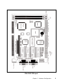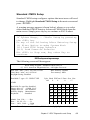
1
PCA-6134P
Half-size 386SX/486SLC CPU Card
with Flash/ROM Disk
User's Manual
Copyright notice
This document is copyrighted, 1994, by Advantech Co., Ltd. All
rights are reserved. Advantech Co., Ltd., reserves the right to make
improvements to the products described in this manual at any time
without notice.
No part of this manual may be reproduced, copied, translated or
transmitted in any form or by any means without the prior written
permission of Advantech Co., Ltd. Information provided in this
manual is intended to be accurate and reliable. However, Advantech Co., Ltd. assumes no responsibility for its use, nor for any
infringements upon the rights of third parties which may result from
its use.
Acknowledgments
AMD is a trademark of Advanced Micro Devices, Inc.
AMI is a trademark of American Megatrends Inc.
IBM, PC AT and VGA are trademarks of International Business
Machines Corporation.
MS-DOS is a trademark of Microsoft Corporation.
SMC is a trademark of Standard Microsystems Corporation
ALI is a trademark of Acer Labs Inc.
Part No. 2006134080 2nd Edition
Printed in Taiwan February 1996
A message to the customer....
Advantech customer services
Each and every Advantech product is built to the most exacting
specifications to ensure reliable performance in the unusual and
demanding conditions typical of industrial environments. Whether
your new Advantech equipment is destined for the laboratory or
the factory floor, you can be assured that it will provide the
reliability and ease of operation for which the name Advantech has
come to be known.
Your satisfaction is our number one concern. Here is a guide to
Advantech’s customer services. To ensure you get the full benefit
of our services, please follow the instructions below carefully.
Technical support
We want you to get the maximum performance from your products.
If you run into technical difficulties, we are here to help. But please
consult this manual first. We have listed the answers to most
commonly asked questions in Appendix E, Maintenance and
troubleshooting.
If you still can’t find the answer, gather all the information or
questions that apply to your problem and, with the product close at
hand, call your dealer. Our dealers are trained and ready to give you
the support you need to get the most from your Advantech
products. In fact, most problems reported are minor and are able to
be easily solved over the phone.
In addition, free technical support is available from Advantech
engineers every business day. We are always ready to give advice
on application requirements or specific information on the installation and operation of any of our products.
Product warranty
Advantech warrants to you, the original purchaser, that each of its
products will be free from defects in materials and workmanship for
one year from the date of purchase.
This warranty does not apply to any products which have been
repaired or altered by other than repair personnel authorized by
Advantech, or which have been subject to misuse, abuse, accident
or improper installation. Advantech assumes no liability as a
consequence of such events under the terms of this Warranty.
Because of Advantech’s high quality-control standards and
rigorous testing, most of our customers never need to use our
repair and replacement service. If an Advantech product ever does
prove defective, it will be repaired at no charge during the warranty
period. For out-of-warranty repairs, you will be billed according to
the cost of replacement materials, service time and freight. Please
consult your dealer for more details.
If you think you have a defective product, follow these steps:
1. Collect all the information about the problem encountered (e.g.
type of PC, CPU speed, Advantech products used, other
hardware and software used etc.). Note anything abnormal and
list any on-screen messages you get when the problem occurs.
2. Call your dealer and describe the problem. Please have your
manual, product and any other information readily available.
3. If your product is diagnosed as defective, obtain an RMA
(return material authorization) number from your dealer. This
allows us to process your return more quickly.
4. Carefully pack the defective product, a completely filled-out
Repair and Replacement Order Card and a photocopy of a dated
proof of purchase (such as your sales receipt) in a shippable
container. A product returned without dated proof of purchase
is not eligible for warranty service.
5. Write the RMA number visibly on the outside of the package
and ship it prepaid to your dealer.
How to use this manual
Thank you for purchasing the PCA-6134P Half-size 386SX/
486SLC/486SLC2 CPU Card with Flash/ROM Disk. We designed this manual to help you quickly and easily set up and install
your card. You can use the manual in two ways:
!Step by step:
The manual guides you through the configuration process from
beginning to end. It gives detailed information to help you make
each configuration choice. Special sections cover tasks such as
installing memory chips, CPU upgrading and watchdog timer setup.
A troubleshooting section lists solutions to common problems.
!Quick start:
Our special Quick Start section (on page 39) gives experienced
users the information they need to setup the CPU card as quickly
as possible. It concisely lists all jumper settings and connections. If
you need more information, it directs you to the page number of the
complete description. If you have any problems, you can work
through the manual step by step for easy troubleshooting.
If you have any questions, feel free to call your local distributor or
sales representative.
Packing list
Before you begin installing your card, please make sure that the
following materials have been shipped:
• 1 PCA-6134P CPU card
• 1 6-pin mini-DIN keyboard adapter
• 1 hard disk drive (IDE) interface cable (40 pin)
• 1 floppy disk drive interface cable (34 pin)
• 1 parallel port adapter (26 pin) kit
• 1 utility disk with Flash/ROM disk utility program
If any of these items are missing or damaged, contact your distributor or sales representative immediately.
Contents
Chapter 1 Hardware Configuration ............................................ 1
Introduction ........................................................................... 2
Specifications ......................................................................... 3
Locating components ........................................................... 4
Jumpers and connectors ....................................................... 6
SIMM memory modules ....................................................... 7
Flash/ROM disk.................................................................... 7
Safety precautions ................................................................. 8
Jumper settings ..................................................................... 8
Card default setting .............................................................. 8
How to set jumpers .............................................................. 9
Display type (JP16) .............................................................. 9
Watchdog timer – system reset/IRQ15 (JP8) ...................... 9
Parallel port IRQ, DACK and DRQ selection
(JP19, JP20, JP21) .......................................................... 10
Parity check (JP23) ............................................................ 10
Chapter 2 Installation ................................................................ 11
Chapter 3 Connecting Peripherals ........................................... 13
Floppy drive connections ................................................... 15
IDE hard drive connections .............................................. 16
Parallel port .......................................................................... 16
Keyboard connectors ......................................................... 17
External switches and indicators ...................................... 17
Reset switch (JP4) ............................................................. 17
Power LED and keylock (JP5) .......................................... 18
Hard disk drive LED (JP3) ................................................ 18
Turbo switch (JP1) ............................................................. 18
Turbo LED (JP2) ................................................................ 19
External speaker ................................................................. 19
SBC power connector......................................................... 19
Serial ports ........................................................................... 20
RS-232 connections ............................................................ 20
RS-232/422/485 serial port connections ............................. 21
Chapter 4 Power-up .................................................................. 25
Chapter 5 BIOS Diagnostics and Setup ................................... 27
POST (Power On Self Tests) ............................................. 28
System test and initialization ............................................... 28
System configuration verification ....................................... 28
Running the setup program ............................................... 29
BIOS Setup Main Menu ..................................................... 30
Standard CMOS Setup ....................................................... 31
Advanced CMOS Setup ..................................................... 35
Auto Configuration with BIOS Defaults ............................ 38
Auto Configuration with Power-On Defaults ..................... 38
Hard Disk Utility ................................................................ 38
Write to CMOS and Exit/Do not Exit ................................. 38
Quick Start for experienced users ............................................ 39
1.
2.
3.
4.
5.
6.
7.
Check card default setting ............................................ 40
Set jumpers ...................................................................... 40
Install memory ................................................................ 41
Install card ....................................................................... 41
Connect peripherals ....................................................... 42
Power up........................................................................... 44
Set up the BIOS .............................................................. 44
Appendix A Flash/ROM Disk ..................................................... 45
Memory devices .................................................................
Drive capacity ....................................................................
Drive configuration .............................................................
Booting from the Flash/ROM disk .....................................
Inserting memory devices...................................................
Formatting the solid state disk ............................................
File copy utility ....................................................................
Using a memory manager (EMM386.EXE) ......................
46
47
47
50
50
50
51
51
Appendix B Programming the Watchdog Timer .................... 53
Programming the watchdog timer .................................... 54
Appendix C Upgrading ............................................................. 55
Installing DRAM (SIMMs) ............................................... 56
Installing PC/104 modules ................................................. 57
Appendix D Detailed System Information ............................... 59
Appendix E Maintenance and Troubleshooting ...................... 71
General maintenance .......................................................... 72
Industrial PC system troubleshooting guide .................. 73
Appendix F AMI BIOS Error Codes .......................................... 77
Power On Self Tests ........................................................... 78
Beep codes ........................................................................... 78
Non-fatal error messages ................................................... 79
Appendix D Card Dimensions ................................................... 91
CHAPTER
1
Hardware
Configuration
This chapter gives background information on the PCA-6134P. It then shows you
how to configure the card to match your
application and prepare it for installation
into your PC.
Sections include:
• Card specifications
• Locating components
• Safety precautions
• Configuration – Jumper settings
Experienced users can skip to the Quick
Start.
Chapter 1 Hardware Configuration
1
Introduction
The half-size PCA-6134P comes equipped with an 80386SX-40 CPU.
Also included on-board are one serial RS-232 port, one serial RS-232/
422/485 port, an enhanced bi-directional parallel port, an IDE hard disk
drive interface (which controls up to 2 IDE hard drives), a floppy disk
controller and a watchdog timer. The watchdog timer ensures that the
CPU will be reset if it stops due to a program or EMI problem, allowing
the PCA-6134P to be used in stand-alone systems or unattended
environments. The PCA-6134P’s industrial-grade construction ensures
continuous, reliable operation in harsh industrial environments at
temperatures up to 140oF (60oC).
We designed the PCA-6134P with SBC (Single Board Computer)
applications in mind. It incorporates a single-voltage power supply (+5
V) and a connector for PC/104 modules (Flat-panel/CRT VGA controller
or Flash/RAM/ROM disk). A built-in Flash/ROM disk emulates a
floppy disk drive of up to 1.44 MB capacity. It emulates the 1st, 2nd,
3rd or 4th DOS drive, depending on the physical disks installed. See
Appendix A for details.
Built using CMOS technology, the PCA-6134P consumes very little
power. Its two SIMM (Single In-line Memory Module) DRAM sockets
accept 1 MB, 4 MB or 16MB SIMM modules for total on-board
memory of 1 to 16 MB.
2
PCA-6134P User's Manual
Specifications
! System
• CPU: 40MHz 80386SX/80486SLC/80486SLC2
• Bus interface: ISA (PC/AT) bus
• Data bus: 16 bit
• DMA channels: 7
• Interrupt levels: 15
• Processing ability: 32 bit
• Bus speed: 8 MHz
• Chipset: ALI M1217
• Real-time clock/calendar:
Uses DS-12887 RTC chip and quartz oscillator, powered by a lithium
battery for 10 years of data retention
! Memory
• RAM memory: 1 MB to 16 MB
Uses 256Kx36, 1Mx36 or 4Mx36 72-pin SIMMs with access time of 80
ns or less
• Shadow RAM memory: Support for system and video BIOS of up to
256 KB in 32 KB blocks
! I/O
• IDE hard disk drive interface: Supports up to two IDE (AT bus)
hard disk drives. BIOS enabled/disabled
• Floppy disk drive interface:
Supports up to two floppy disk drives, 5.25” (360 KB and 1.2 MB)
and/or 3.5” (720 KB and 1.44 MB). BIOS enabled/disabled
• Enhanced bi-directional parallel port: Configurable to LPT1, LPT2,
LPT3 or disabled. Standard female DB-25 connector provided
• Serial ports: One serial RS-232 port, one serial RS-232/422/485 port.
Ports can be individually configured as COM1, COM2 or disabled
Chapter 1 Hardware Configuration
3
! Industrial features
• Watchdog timer:
Software programmable ON/OFF. The time-out interval is programmable in 12 levels (0.5 seconds ~ 16 minutes 48 seconds). Your
program uses hex 043 and 443 to control the watchdog. The watchdog can reset the system or generate an interrupt.
• PC/104 connector:
A PC/104 connector for industry-standard PC/104 modules such as a
Flash/RAM/ROM disk module and/or Flat-panel/CRT VGA module
• Keyboard connectors: A 6-pin mini-DIN keyboard connector is
located on the mounting bracket for easy access. An external
keyboard adapter is included. An on-board keyboard pin header
connector is also available.
! General
• Max power required: + 5 V @ 2 A
• Power supply voltage: +5 V (4.75 V to 5.25 V)
• Operating temperature: 32 to 140oF (0 to 60oC)
• Size: 7.3" (L) x 4.8" (W) (185 mm x 122 mm)
• Weight: 1.1 lbs (0.5 kg)
Locating components
This section identifies the location of the card's major components. It
also includes a list of the function of each of the card jumpers. The
figure on the following page gives an overall view of the card.
4
PCA-6134P User's Manual
PCA-6134P PCB layout
Chapter 1 Hardware Configuration
5
Jumpers and connectors
Connectors on the board link it to external devices such as hard disk
drives, a keyboard or PC/104 module. In addition, the board has a
number of jumpers which you use to configure it for your application.
The table below lists the function of each of the board jumpers and
connectors. Later sections in this chapter give instructions on setting
jumpers and detailed information on each jumper setting. Chapter 3
gives instructions for connecting external devices to your card. Pin
assignments for each connector appear there or in Appendix D.
Jumpers and connectors
Number
J1
6
Function
Keyboard connector
Page
17
J2
SBC Power Connector
19
J3
Keyboard connector (6-pin mini-DIN)
17
JP1
Turbo switch
18
JP2
Turbo LED
19
JP3
Hard disk drive activity LED
18
JP4
Reset switch
17
JP5
Power LED and keylock
18
JP7
Speaker connector
19
JP8
Watchdog timer:
System reset / generate interrupt IRQ15
9
JP9, 10, 11
SSD device selection
46
J14, 15, 18,
22, 24, 25,
28, 29
RS-232/422/485 selection
21
JP16
Display type: color/mono
9
JP19
Parallel port IRQ selection
10
JP20
Parallel port DACK selection
10
JP21
Parallel port DRQ selection
10
JP23
Parity check enable/disable
10
PCA-6134P User's Manual
Jumpers and connectors, cont.
Number Function Page
CN1
HDD connector
16
CN2
FDD connector
15
CN3
Parallel/printer connector
16
CN4/CN5
PC/104 connector
57
COM1
RS-232 serial port
20
COM2
RS-232/422/485 serial port
21
SIMM memory modules
On the left end of the card (away from the mounting bracket) are the
two SIMM (Single In-line Memory Module) sockets which hold the
card’s DRAM memory. If you ordered DRAM SIMMs along with your
card, the SIMMs may already be installed. If not, you should install
them as described in Appendix C.
Flash/ROM disk
At the right of the card are three 32-pin sockets which hold the
memory chips for the card's Flash/ROM disk. Instructions for installing
memory chips appear in Appendix A.
Chapter 1 Hardware Configuration
7
Safety precautions
Follow these simple precautions to protect yourself from harm and
your PC from damage.
1. To avoid electric shock always disconnect the power from your PC
chassis before you work on it. Don’t touch any components of the
CPU card or other cards while the PC is on.
2. Disconnect power before making any configuration changes. The
sudden rush of power as you connect a jumper or install a card may
damage sensitive electronic components.
3. Always ground yourself to remove any static charge before you
touch your CPU card. Be particularly careful not to touch the chip
connectors. Modern integrated electronic devices, especially CPUs
and memory chips, are extremely sensitive to static electric discharges and fields. Keep the card in its anti-static packaging when
it is not installed in the PC and place it on a static dissipative mat
when you are working on it. Wear a grounding wrist strap for
continuous protection.
Jumper settings
This section tells how to set the jumpers to configure your card. It
gives the card default configuration and your options for each jumper.
After you set the jumpers and install the card, you will also need to run
the BIOS Setup program (discussed in Chapter 5) to configure the
serial port addresses, floppy/hard disk drive types and system
operating parameters. Connections, such as hard-disk cables, appear
in Chapter 3.
Card default setting
We set the card’s jumpers at the factory for the most popular configuration. If this configuration matches your needs, you may not need to
change the jumpers at all. The default configuration is as follows:
• Watchdog invokes system reset
• Parallel port IRQ7, DRQ1, DACK1
8
PCA-6134P User's Manual
• Parity checking enabled
• Color display attached
How to set jumpers
You configure your card to match the needs of your application by
setting jumpers. A jumper is the simplest kind of electric switch. It
consists of two metal pins and a small metal clip (often protected by a
plastic cover) that slides over the pins to connect them. To “close” a
jumper you connect the pins with the clip. To “open” a jumper you
remove the clip. Sometimes a jumper will have three pins, labeled 1, 2
and 3. In this case you would connect either pins 1 and 2 or 2 and 3.
You may find pair of needle-nose pliers useful for setting the jumpers.
If you have any doubts about the best hardware configuration for
your application, contact your local distributor or sales representative
before you make any changes.
Display type (JP16)
This jumper sets the display adapter type attached to your card. If you
are using a monochrome LCD or EL screen which uses a CGA, EGA,
VGA or other color display adapter, set JP16 to color. The next table
shows the available jumper settings:
Display type selection
JP16
Open
Setting
Monochrome
Closed
Color (default)
Watchdog timer – system reset/IRQ15 (JP8)
When the watchdog timer activates (CPU processing has come to a
halt), it can reset the system or generate an interrupt on IRQ15. Set JP8
as shown in the following table:
Watchdog timer setup
JP8
1-2
Setting
System reset (default)
2-3
IRQ15
Chapter 1 Hardware Configuration
9
Parallel port IRQ, DACK and DRQ
selection (JP19, JP20, JP21)
You can set the IRQ (JP19), DACK (JP20) and DRQ (JP21) of the
parallel port. The following tables show the available options :
Parallel port IRQ selection
JP19
1-2
IRQ no
IRQ7 (default)
2-3
IRQ5
Parallel port DACK selection
JP20
1-2
DACK no
DACK1 (default)
2-3
DACK3
Parallel port DRQ selection
JP21
1-2
DRQ no
DRQ1 (default)
2-3
DRQ3
Parity check (JP23)
You can set the parity checking to enabled/disabled. If you use
memory without a parity bit, you must disable parity checking.
The next table shows the options:
Parity check options
10
JP23
Open
Setting
Enabled (default)
Closed
Disabled
PCA-6134P User's Manual
CHAPTER
2
Installation
This chapter gives a general procedure for
installing your CPU card into an PC
chassis with an AT-compatible passive
backplane. For specific instructions,
consult the user’s manual for your
chassis.
Before you begin, double check the
jumper settings for the card (described in
Chapter 1). This could save you a lot of
troubleshooting time later. If you are not
sure about the proper setting, contact
your local distributor or sales representative.
Chapter 2 Installation
11
Warning! Disconnect all power from the chassis before you
install the CPU card. Unplug the power cord from
the wall, don’t just turn off the power switch. If you
are not sure what to do, take the job to an experienced professional.
Caution!
The electronic components on this CPU card are
very sensitive to static electric charges. Use a
grounding wrist strap to remove all static electricity before you touch any components. Place all
components on a static-dissipative mat or in a
static-shielded bag when they are not in the
chassis.
Install your CPU card as follows:
1. Remove power from the chassis and disconnect all power
cords. Follow all power-down procedures outlined in your
chassis user’s manual.
2. Remove the chassis cover, then detach the card hold-down
bracket. This bracket stretches across the top of each circuit
card to hold it securely in place.
3. Locate a free slot in the chassis. You can use any 16-bit (double
connector) slot. We suggest that you leave the maximum
amount of space between boards to improve cooling.
4. You may need to remove a block-off cover at the end of the slot.
Unscrew the cover and save the screw for use in Step 6.
5. Align the card square with the card-end guide slot and parallel
to the connector. Slide the card carefully into the connector.
6. Make sure the card is completely seated in the connector.
Fasten the card I/O bracket to the case with the screw.
After you have installed the CPU card, you will need to attach the
connecting cables as described in the following chapter. When you
are finished installing the CPU card, replace the card hold-down
bracket you removed in Step 2, replace the chassis cover and
power-up your system.
Dimensions for SBC (Single Board Computer) installation appear on
page 10.
12
PCA-6134P User's Manual
CHAPTER
3
Connecting
Peripherals
This chapter tells how to connect peripherals, switches and indicators to the
PCA-6134P board. You can access most of
the connectors from at the top of the
board while it is installed in the chassis. If
you have a number of cards installed, or
your chassis is very tight, you may need
to partially remove the card to make all the
connections. When everything is done,
finish installing the card as described in
Chapter 2.
Chapter 3 Connecting Peripherals
13
The following table lists the connectors on the PCA-6134P. See
Chapter 1 for help locating the connectors.
Component
HDD (IDE) connector
FDD connector
Parallel port
PC/104 connector
Keyboard connectors
Reset switch connector
Power LED and keylock connector
HDD LED connector
Turbo switch connector
Turbo LED connector
External speaker connector
SBC power connector
RS-232 serial port
RS-232/422/485 serial port
Label
CN1
CN2
CN3
CN4, CN5
J1, J3
JP4
JP5
JP3
JP1
JP2
JP7
J2
COM1
COM2
Page
16
15
16
57
17
17
18
18
18
19
19
19
20
21
The following sections tell how to make each connection. In most
cases you will simply need to connect a standard cable. If you need
to make your own cables, you can find pin assignments for the
more complicated connectors in Appendix D.
Warning! Always completely disconnect the power cord
from your chassis whenever you are working on it.
Do not make connections while the power is on,
sensitive electronic components can be damaged
by the sudden rush of power. Only experienced
electronics personnel should open the PC chassis.
Caution!
14
Always ground yourself to remove any static
charge before touching the CPU card. Modern
electronic devices are very sensitive to static
electric charges. Use a grounding wrist strap at all
times. Place all electronic components on a
static-dissipative surface or in a static-shielded
bag when they are not in the chassis.
PCA-6134P User's Manual
Floppy drive connections
You can attach up to two floppy disk drives to the PCA-6134P's onboard controller. You can use any combination of 5.25"
(360 KB and 1.2 MB) and/or 3.5" (720 KB and 1.44 MB) drives.
The card comes with a 34-pin daisy-chain drive connector cable.
On one end of the cable is a 34-pin flat-cable connector. On the
other end are two sets of floppy disk drive connectors. Each set
consists of a 34-pin flat-cable connector (usually used for 3.5"
drives) and a printed-circuit-board connector (usually used for
5.25" drives). You can use only one connector in each set. The set
on the end (after the twist in the cable) connects to the A: floppy.
The set in the middle connects to the B: floppy.
Attach the single 34-pin flat-cable connector to CN2 on the CPU
card. For help finding the connector, see Chapter 1. Wire number 1
on the cable is red or blue, the other wires are gray. Make sure that
the red wire corresponds to pin one on the connector (on the right
side).
Connect the A: floppy drive to the connector set on the other end
of the cable. If you are connecting a 5.25" floppy drive, line up the
slot in the printed-circuit-board (golden fingers) with the blockedoff part of the cable connector.
If you are connecting a 3.5" floppy drive, you may have trouble
determining which pin is number one. Look for a number printed on
the circuit board indicating pin number one. Also, the connector on
the floppy drive connector may have a slot. When the slot is up,
pin number one should be on the right. Check the documentation
that came with the drive for more information.
Next, if you desire, connect the B: floppy drive to the connectors in
the middle of the cable as described above.
If you need to make your own cable, you can find the pin assignments for the card’s connector in Appendix D.
Chapter 3 Connecting Peripherals
15
IDE hard drive connections
You can attach two IDE (Integrated Device Electronics) hard disk
drives to the PCA-6134P internal controller. The card comes with a
40-pin flat-cable piggyback cable. This cable has three identical 40pin flat-cable connectors.
Wire number 1 on the cable is red or blue, the other wires are gray.
Connect one end to connector CN1 on the CPU card. Make sure
that the red wire corresponds to pin one on the connector (on the
right side). See Chapter 1 for help finding the connector.
Unlike floppy drives, IDE hard drives can connect in either position
on the cable. If you install two drives, you will need to set one as
the master and one as the slave. You do this using jumpers on the
drives. If you use just one drive, you should set it as the master.
See the documentation that came with your drive for more information.
Connect the first hard drive to the other end of the cable. Wire one
on the cable should also connect to pin one on the hard drive
connector. You may have difficulty determining the pin number.
Look for a number printed on the drive circuit board. Also, the
connector on the floppy drive connector may have a slot. When
the slot is up, pin number one should be on the right. Check the
documentation that came with the drive for more information.
Connect a second drive as described above.
If you need to make your own cable, you can find the pin assignments for the card’s connector in Appendix D.
Parallel port
You would normally use the parallel port to connect the card to a
printer. The PCA-6134P includes an on-board parallel port, accessed through a 26-pin flat-cable connector, CN3. The CPU card comes
with an adapter cable which lets you use a traditional DB-25
connector. The cable has a 26-pin connector on one end and a
16
PCA-6134P User's Manual
DB-25 connector on the other, mounted on a retaining bracket. The
bracket installs at the end of an empty slot in your chassis, giving
you access to the connector.
To install the bracket find an empty slot in your chassis. Unscrew
the plate that covers the end of the slot. Screw in the bracket in
place of the plate. Next, attach the flat-cable connector to connector CN3 on the CPU card. Wire one of the cable is red or blue, the
other wires are gray. Make sure that wire one connects to pin one
of CN3. Pin one is on the right side of CN3. For help finding the
connector, see the figure on page 5.
The pin assignments for the connector appear in Appendix D.
Keyboard connectors
The PCA-6134P board provides two keyboard connectors. A 5-pin
connector (J1) supports passive backplane applications. A second
6-pin mini-DIN connector (J3) on the card mounting bracket
supports single-board-computer applications. The card comes with
an adapter to convert from the 6-pin mini-DIN connector to a
standard DIN connector.
If you need to make your own adapter cable, you can find the pin
assignments in Appendix D.
External switches and indicators
Next you may want to install external switches to monitor and
control your CPU card. These features are completely optional —
install them only if you need them.
Reset switch (JP4)
You can connect an external switch to easily reset your computer.
This switch restarts your computer as if you had turned off the
power then turned it back on. Install the switch so that it closes the
two pins of JP4.
Chapter 3 Connecting Peripherals
17
Power LED and keylock (JP5)
You can connect an LED to indicate when the CPU card is on. Pin 1
of JP5 supplies power to the LED and Pin 3 is the ground. For help
finding JP5 see the figure on page 5.
You can use a switch (or a lock) to disable the keyboard. In this
state the PC will not respond to any input. This is useful if you
don’t want anyone to change or stop a running program. Simply
connect the switch between Pins 4 and 5 of JP5. The pin assignments for JP5 appear in the following table:
Power LED and keylock (JP5)
Pin
1
2
3
4
5
Function
LED Power (+5 V)
No Connection
Ground
Keyboard lock
Ground
Hard disk drive LED (JP3)
You can connect a LED to connector JP3 to indicate when the HDD
is active. Marks on the circuit board indicate LED polarity (the pin
on the left is positive).
Turbo switch (JP1)
You can connect a switch across the pins of jumper JP1 to change
the CPU between Turbo and non-Turbo mode. When you close
(short) the pins, the CPU card operates at full speed. When you
leave the pins open, the card operates at slow speed for compatibility with older software.
You can also switch the CPU back and forth between Turbo mode
and non-Turbo mode using the keyboard, but only when jumper
JP1 is open. When jumper JP1 is closed, the CPU is fixed in Turbo
mode. To switch into Turbo mode from the keyboard simultaneously press the Ctrl, Alt and keypad plus (+) keys. To switch into nonTurbo mode press the Ctrl, Alt and keypad minus (-) keys.
18
PCA-6134P User's Manual
Turbo LED (JP2)
You can connect a LED indicator across jumper JP2 to indicate
when the CPU is in Turbo mode. Marks on the circuit board
indicate LED polarity (the pin on the right is positive).
External speaker
The CPU card has its own buzzer. You can also connect to the
external speaker on your computer chassis. Connect leads to
connector JP7 as shown below:
External speaker (JP7)
Pin
1
2
3
4
Function
+5 VDC
Speaker out
Speaker out
Speaker out
SBC power connector
In single-board-computer (non-passive-backplane) applications
you will need to connect power directly to the PCA-6134P board
using connector J2. This connector is fully compatible with the
standard PC power supply connector for a 3.5" FDD (or HDD). See
the following table for its pin assignments:
SBC power connector (J2)
Pin
1
2
3
4
Function
+5 VDC
GND
GND
+12 VDC
Chapter 3 Connecting Peripherals
19
Serial ports
The PCA-6134P offers two serial ports: one RS-232 and one
RS-232/422/485. These ports let you connect to serial devices (a
mouse, printers, etc.) or a communication network.
You can select the address for each port (3F8H [COM1], 2F8H
[COM2] or 3E8H) or disable it, using the BIOS Advanced Setup
program, covered in Chapter 5.
The card mounting bracket holds the serial port connectors. This
lets you connect and disconnect cables after you install the card.
The DB-9 connector on the top of the bracket is the RS-232 port.
The second DB-9 connector is the RS-232/422/485 port. The
following sections tell how to make RS-232 and RS-232/422/485
connections.
RS-232 connections
Different devices implement the RS-232 standard in different ways.
If you are having problems with a serial device, be sure to check
the pin assignments for the connector. The following table shows
the pin assignments for the card's RS-232 port:
RS-232 connector pin assignments
Pin
1
2
3
4
5
6
7
8
9
20
Signal
DCD
RX
TX
DTR
GND
DSR
RTS
CTS
RI
PCA-6134P User's Manual
RS-232/422/485 serial port connections
RS-422 and RS-485 are popular for industrial and laboratory
communication because they offer high noise resistance and long
range (up to 4000 ft, 1200 m). RS-422 is commonly used for two-way
communication between two devices, whereas RS-485 is used for
communication between a single master and a network of slave
modules.
Before you use the RS-232/422/485 port, you will need to select
RS-232, RS-422 (the default) or RS-485 mode. Set jumpers JP14, 15,
17, 18, 22, 24 and JP25 according to the following table:
JP14
JP15
JP28
JP29
RS-232
1-2
Open
Open
Open
RS-422 (def.)
2-3
1-2
Short
Short
RS-485
2-3
2-3
Short
Short
JP18
JP22
Open
Open
Open
Open
Short
Short
JP24
JP25
1-2
Open
2-3
Short
2-3
Short
For RS-422/485 the pin assignments for the DB-9 connector will be
as follows:
RS-422/485 connector pin assignments
Pin
1
2
3
4
5
6
7
8
9
Signal
TX - or send data - (DTE)
TX + or send data + (DTE)
RX + or receive data + (DTE)
RX - or receive data - (DTE)
Ground
RTS - or ready to send RTS + or ready to send +
CTS + or clear to send +
CTS - or clear to send -
Chapter 3 Connecting Peripherals
21
!RS-422 signal wiring
RS-422 is used for long-distance point-to-point connections.
RS-422 originally used four wires for one-way communication (with
devices such as display terminals or printers) but was later adopted
by industry for simultaneous two-way communication by doubling
the number of wires.
Each pin on the first device connects to a corresponding device on
the second. Flow control lines manage the communication. The
following table shows pin connections:
Computer A
Computer B
Pin
1
2
3
4
5
6
7
8
9
Pin
4
3
2
1
5
9
8
7
6
Signal
TXTX+
RX+
RXGND
RTSRTS+
CTS+
CTS-
>
>
<
<
<
>
>
>
<
<
Signal
RXRX+
TX+
TXGND
CTSCTS+
RTS+
RTS-
!RS-485 signal wiring
In a typical RS-485 application the host device requests data from a
slave module then listens for the response. The host transmits and
receives data on the same pair of wires. Software handles the flow
control; no other wires are needed.
Pin assignments appear in the following table. Pins 1 and 4 share
the Data+ wire. Pins 2 and 3 share the Data- wire.
22
Computer A
Device B
Pin
1
4
2
3
5
Pin
1
4
2
3
5
Signal
TX- –
RX- –
TX+ –
RX+ –
GND
DataData+
PCA-6134P User's Manual
–
–
–
–
Signal
TXRXTX+
RX+
GND
RS-422/RS-485 driver and receiver circuit
The following figure shows the circuits for the card's RS-422 and
RS-485 driver and receiver.
Driver and receiver circuit
Now that you have made all the required external connections, you
can close up your chassis (as described in Chapter 2). If you are
installing any other cards, do it now. You can then power up your
system as described in the next chapter.
Chapter 3 Connecting Peripherals
23
24
PCA-6134P User's Manual
CHAPTER
4
Power-up
After you have set the jumpers (Chapter 1),
installed SIMMs (Appendix C), installed the
card (Chapter 2) and made all external
connections (Chapter 3), you are ready to
power-up your system.
Chapter 4 Power-up
25
Follow the startup procedure outlined in the manual for your
chassis.
When you start your system, the BIOS will test the hardware and
check the system configuration against the values stored in its
CMOS memory.
Since this is the first time you are starting up, the BIOS will display
an error message stating that the configuration does not match the
stored values. You should then run the BIOS setup program as
described in Chapter 5.
If the BIOS hardware diagnostic tests fail, you may see an error
message on the screen describing the problem. If the BIOS found a
problem early in the tests, you will need to determine the BIOS
POST (Power On Self Test) results by counting beeps or using a
POST card. See Appendix F for details.
The most common source of problems is incorrect jumper settings.
Double check your settings (Chapter 1) and restart the system. If
the system still has problems, see Appendix E, Maintenance and
troubleshooting.
There are three methods you can use to restart your system after it
is turned on:
1. Switch the power off, then on again
2. Reboot the system. Using the keyboard, simultaneously press
the CTL, ALT and DEL keys
3. Depress the optional reset switch
Use of each of these methods will erase data from the system RAM
memory. If you can, save any data stored in memory to a hard or
floppy disk before you reset your system.
26
PCA-6134P User's Manual
CHAPTER
5
BIOS Diagnostics
and Setup
This chapter describes the card’s diagnostic tests and how to set BIOS configuration data. BIOS POST (Power On Self
Test) test codes appear in Appendix F.
Chapter 5 BIOS Diagnostics and Setup
27
POST (Power On Self Tests)
Whenever you start up your system, the CPU card runs a series of
programs stored in an on-board ROM chip. These programs are
divided into two stages:
System test and initialization
These routines test and initialize board hardware. If the routines
encounter an error during the tests, you will either hear a few short
beeps or see an error message on the screen. There are two kinds
of errors: fatal and non-fatal. The system can usually continue the
boot up sequence with non-fatal errors. Non-fatal error messages
usually appear on the screen along with the following instructions:
press <F1> to RESUME
Write down the message and press the F1 key to continue the
bootup sequence. Non-fatal error messages appear in Appendix F.
If the routines encounter a fatal error, they will stop the tests and
output a message indicating which test failed. If the fatal error
comes before the screen device initializes, the card will indicate the
error code through a series of beeps. Error beep codes also appear
in Appendix F.
System configuration verification
These routines check the current system configuration against the
values stored in the card’s CMOS memory. If they don’t match, the
program outputs an error message. You will then need to run the
BIOS setup program to set the configuration information in
memory.
28
PCA-6134P User's Manual
There are three situations in which you will need to change the
CMOS settings:
1. You are starting your system for the first time
2. You have changed the hardware attached to your system
3. The CMOS memory has lost power and the configuration
information has been erased.
The PCA-6134P’s CMOS memory has integral lithium battery
backup. The battery backup should last ten years in normal service,
but when it finally runs down, you will need to replace it. Contact
your sales representative or distributor for details.
Running the setup program
Normally, the only routine visible on the screen will be the memory
test. The following figure shows the screen as it appears while the
tests are occurring.
ROM BIOS(c) 1990 American Megatrends, Inc
xxxx KB OK
Hit <DEL> if you want to run SETUP
(c)American Megatrends, Inc.
xx-xxxx-xxxxxx-xxxxxxx-xxxxxx-xxxx
Power On Self Tests
A line of reference codes appears at the bottom left of the screen.
These codes identify the options installed in the AMI BIOS. If you
have a problem with your system, make a note of these codes
before you contact your dealer for technical support.
To “freeze” the screen so that you can write down the codes,
power-on the system and hold down a key on the keyboard. This
will cause a “Keyboard Error” message to appear on the screen and
the system will wait for you to press the <F1> key. After you copy
Chapter 5 BIOS Diagnostics and Setup
29
down the line, you can then press <F1> to continue the boot
procedure. After the POST routines are complete, the following
message appears:
Hit <DEL> if you want to run SETUP
Press the <DEL> key to access the BIOS setup program. The
following screen will then appear.
BIOS Setup Main Menu
You use the following keys to control the BIOS SETUP program:
ESC: Exit to previous screen
ARROW KEYS: Moves the cursor to highlight the desired
configuration option
PAGEUP/PAGEDOWN/CTRL-PAGEUP/CTRL-PAGEDOWN:
Cycles through the configuration options for the highlighted
feature. If there are less than ten available options, the CtrlPageUp and Ctrl-PageDown keys function the same as the
PageUp and PageDown keys.
F1: Displays a help screen for selected feature.
F2/F3: Changes background and foreground colors.
F5: Retrieves the values which were resident when the current
setup session was started. These values will be CMOS values
if the CMOS was uncorrupted at the start of the session, or
they will be the BIOS Setup default values.
F6: Loads all features in the Advanced CMOS Setup with the
BIOS Setup defaults.
F7: Loads all features in the Advanced CMOS Setup with the
Power-On defaults (the values in the CMOS when the system
was started).
F10: Saves all changed made to Setup and exits program.
30
PCA-6134P User's Manual
Standard CMOS Setup
Standard CMOS setup configures options that most users will need
to change. Highlight Standard CMOS Setup in the main screen and
press <ENTER>.
A warning message appears (shown below) whenever you select
either Standard CMOS Setup or Advanced CMOS Setup from the
main screen. Simply press any key to continue or ESC to abort.
Improper Use of Setup may Cause Problems!!
If System Hangs,.....Enter Setup by pressing
the <DEL> key
Do any of the following After Entering Setup
(i) Alter Option to make System Work
(ii) Load BIOS Setup Defaults
(iii) Load Power-On Defaults
Hit <ESC> to Stop now, Any other Key to
continue
BIOS setup warning message
The following screen will then appear:
BIOS Setup Program - Standard CMOS SETUP
(C) 1991, American Megatrends Inc., All Rights Reserved
Date (mn / date / year): Tue, Jan 01 1991
Time (hour / min / sec): 09:39:06
Daylight Saving: Disabled
Hard disk C: type: 47= USER TYPE
Base memory: 640KB
Ext. memory: 0KB
Cyln Head WPCom LZone Sect Size
642
8
0
0
17
43MB
Hard disk D: type:Not Installed
Floppy drive A: :1.2MB, 51/4"
Floppy drive B: :Not Installed
Primary display :Monochrome
Keyboard
:Installed
Sun Mo Tue We Thu Fri Sat
30
31
1
2
3
4
5
6
7
8
9
10
11
12
13
14
15
16
17
18
19
20
21
22
23
24
25
26
27
28
29
30
31
1
2
Month: Jan, Feb,...........Dec
Date : 01, 02, 03..........31
3
4
5
6
7
8
Year : 1901, 1902.........2099
←→↓↑
Esc = Exit,
= Select, F2/F3 = Color, PgUp/PgDn = Modify
Chapter 5 BIOS Diagnostics and Setup
9
31
This screen lets you set following features:
Date:
System date. A prompt box at the lower left corner of the screen
gives the range of allowable values.
Time:
System clock. Hour first, minute then second. Uses 24 hour
clock format (for PM numbers add 12 to the hour: you would
enter 4:30 p. m. as 16:30:00)
Daylight Savings: Disabled or Enabled
Hard Disk C: and Hard Disk D:
The BIOS supports 46 standard hard disk sizes and layouts. If
your hard disk matches one of these types (shown below),
highlight the number blank (for the appropriate drive, C: or D:)
and press <PgDn> until the correct number appears. If the BIOS
does not support your hard disk, select disk type 47 and enter
each of the specifications into the blank (e. g. number of cyln.).
You can get these numbers from a label on your disk drive or
from the documentation that came with the drive. After you
have set up drive C:, you can then set up drive D:. If you have
no drive D:, select Not Installed.
Hard disk types
Type
1
2
3
4
5
6
7
8
9
10
11
12
13
32
Cyln
306
615
615
940
940
615
462
733
900
820
855
855
306
Head
4
4
6
8
6
4
8
5
15
3
5
7
8
PCA-6134P User's Manual
WPcomp
128
300
300
512
512
65535
256
65535
65535
65535
65535
65535
128
LZone
305
615
615
940
940
615
511
733
981
828
855
855
319
Sect
17
17
17
17
17
17
17
17
17
17
17
17
17
Size
10 MB
20 MB
31 MB
62 MB
47 MB
20 MB
31 MB
30 MB
112 MB
20 MB
35 MB
50 MB
20 MB
Type
14
16
17
18
19
20
21
22
23
24
25
26
27
28
29
30
31
32
33
34
35
36
37
38
39
40
41
42
43
44
45
46
47
Cyln
733
612
977
977
1024
733
733
733
306
925
925
754
754
699
823
918
1024
1024
1024
612
1024
1024
615
987
987
820
977
981
830
830
917
1224
user type
Head
7
4
5
7
7
5
7
5
4
7
9
7
11
7
10
7
11
15
5
2
9
8
8
3
7
6
5
5
7
10
15
15
WPcomp
65535
0
300
65535
512
300
300
300
0
0
65535
754
65535
256
65535
918
65535
65535
1024
128
65535
512
128
987
987
820
977
981
512
65535
65535
65535
LZone
733
663
977
977
1023
732
732
733
336
925
925
754
754
699
823
918
1024
1024
1024
612
1024
1024
615
987
987
820
977
981
830
830
918
1223
Sect
17
17
17
17
17
17
17
17
17
17
17
17
17
17
17
17
17
17
17
17
17
17
17
17
17
17
17
17
17
17
17
17
Size
43 MB
20 MB
41 MB
57 MB
60 MB
30 MB
43 MB
30 MB
10 MB
54 MB
69 MB
44 MB
69 MB
41 MB
68 MB
53 MB
94 MB
128 MB
43 MB
10 MB
77 MB
68 MB
41 MB
25 MB
57 MB
41 MB
41 MB
41 MB
48 MB
69 MB
114 MB
152 MB
Note that the user definition entry (47) lets you define a disk
drive not defined in ROM. You have to supply all the relevant
information concerning the drive characteristics. This is usually
found on a label on the disk or in the disk's documentation.
Chapter 5 BIOS Diagnostics and Setup
33
The following chart shows the meaning of each of the hard disk
parameters:
Hard disk parameters
Type:
Cyl:
Heads:
WPpcom:
L-Zone:
Capacity:
This is the number designation for a drive with
certain identification parameters.
This is number of cylinders found in the specified
drive type.
This is the number of heads found in the specified drive
type.
WPcom is the read delay circuitry which takes into account
the timing differences between the inner and outer edges of
the surface of the disk platter. The number designates the
starting cylinder of the signal.
LZone is the landing zones of the heads. This number
determines the cylinder location where the heads will
normally park when the system is shut down.
This is the formatted capacity of the drive based on the
following formula:
(# of heads) x (# of cylinders) x (# of sectors) x (512
bytes/sec)
Floppy Drive A: and Floppy Drive B:
The BIOS supports any combination of 3.5" (720 KB and
1.44 MB) and 5.25" (360 KB and 1.2 MB) floppy disks. If you
have no floppy disk installed, select Not Installed.
Primary Display:
Select the type of display you have connected. Options are:
Monochrome, Color 40x25, VGA/PGA/EGA, Color 80x25 and
Not Installed. You might use the Not installed option for a
network file server.
Keyboard:
Options are Installed or Not Installed.
Note: If you are running your system on a non-dedicated file
server, and you do not want the AMI BIOS to report any
keyboard, video or floppy disk drive errors during POST, set the
AMI BIOS Keyboard, Primary display and floppy disk features
to “Not Installed.”
34
PCA-6134P User's Manual
Advanced CMOS Setup
Advanced CMOS Setup controls system settings and the
ALI M1217 chipset’s configuration registers. Adjusting these
parameters may improve system performance, but make a note of
the original settings before you make any changes. Some combinations of settings may cause your system to crash or become
unreliable.
From the main menu highlight the Advanced CMOS Setup option
and press <ENTER>. Press any key to clear the warning screen.
! Features
The following chart lists card settings which you can change in
Advanced CMOS Setup. It lists the default value for each setting.
This screen has several help screens, accessed by pressing the
<F1> key, which display setting options.
Feature
Available options
Typematic Rate Programming
Disabled (default)
Enabled
Typematic Rate Delay (msec)
500 (default)
Typematic Rate (Chars/sec)
30 (default)
Above 1MB Memory Test
Disabled (default)
Memory Test Tick Sound
Enabled (default)
Disabled
Memory Parity Error Check
Enabled (default)
Disabled
Hit <DEL> Message Display
Enabled (default)
Disabled
Hard Disk Type 47 RAM Area
0:300 (default)
DOS 1KB
This setting determines where in memory the hard disk information is
stored when you select hard disk type 47. If you disable BIOS Shadow
RAM, the Hard Disk Type 47 parameter table will use regular RAM. There
are two options, 0:300 (lower system RAM) and DOS 1 KB (the top 1KB
of 640 KB base memory).
Wait for <F1> if Any Error
Enabled (default)
Disabled
System Bootup Num Lock
On (default)
Off
Chapter 5 BIOS Diagnostics and Setup
35
Feature
Floppy Drive Seek At Boot
Available options
Enabled (default)
Disabled
System Bootup Sequence
A:, C: (default)
C:, A:
System Boot-up CPU speed
High (default)
Low
Turbo Switch Function
Enabled (default)
Disabled
Password Checking Option
Setup (default)
Always
Video ROM Shadow
Enabled (default)
C000,32K
Disabled
Adapter ROM Shadow
Disabled (default)
C800,32K
Enabled
Adapter ROM Shadow
Disabled (default)
D000,32K
Enabled
Adapter ROM Shadow
Disabled (default)
D800,32K
Enabled
Adapter ROM Shadow
Disabled (default)
E000, 32K
Enabled
Adapter ROM Shadow
Disabled (default)
E800,32K
Enabled
The above settings shadow ROMs on plug-in cards. You will need to
know the addresses of the ROMs.
Boot Sector Virus Protection
Disabled (default)
Enabled
IDE Block Mode Transfer
Disabled (default)
Enabled
Serial Port 1
3F8H (default)
2F8H
3E8H
Disabled
Serial Port 2
2F8H (default)
3F8H
2E8H
Disabled
36
PCA-6134P User's Manual
Feature
Parallel Port
Parallel Port Mode
IDE Controller
Floppy Controller
Watchdog Timer Setting
Available options
378H (default)
278H
3BCH
Disabled
Normal (default)
ECP + EPP
ECP
EPP
Bi-direction
Enabled (default)
Disabled
Enabled (default)
Disabled
16 min
08 min
04 min
02 min
01 min
48 seconds
24 seconds
12 seconds
06 seconds
03 seconds
31.5 seconds
15.8 seconds
7.9 seconds
3.9 seconds
2.0 seconds (default)
1.0 seconds
0.5 seconds
Disabled
Internal Flash/ROM disk
Disabled (default)
Enabled
After you have made your configurations changes, press <ESC> to
return to the main menu.
Chapter 5 BIOS Diagnostics and Setup
37
Auto Configuration with BIOS Defaults
This main menu option loads the system default values stored in
the BIOS ROM at the factory.
Auto Configuration with Power-On Defaults
This main menu option loads the settings stored in the CMOS
memory when you turned on your system. If your system behaves
erratically, you can use this feature to check for incorrect settings.
Hard Disk Utility
This option lets you perform low-level hard disk drive preparation
before you use the DOS FDISK or FORMAT utilities. All of its
functions are destructive to existing data on the disk drive.
Most IDE hard drives come preformatted from the factory, so you
will probably only need these utilities if your hard disk develops
bad sectors or ages and needs to have the formatting information
refreshed.
Write to CMOS and Exit/Do not Exit
After you have made your configuration changes, select Write to
CMOS and Exit. If you decide you want to abandon the changes
you have made, select Do not Write to CMOS and Exit.
The BIOS will then perform a memory test, and attempt to boot
your system.
Be sure that your DOS system files are located on either drive A: or
on your hard disk drive. If they are not, the BIOS will not be able to
boot your system.
38
PCA-6134P User's Manual
Quick
Start
for experienced
users
This Quick Start section puts all the vital
configuration information in one place. If
you need more information about any
setting, just check the appropriate page
reference.
Quick Start for experienced users
39
1.
Check card default setting
We set the card’s jumpers at the factory for the most popular
configuration. If this configuration matches your needs, you can
skip to step 3. The default configuration is as follows:
• Watchdog invokes system reset
• Parallel port IRQ7, DRQ1, DACK1
2.
• Parity checking enabled
• Color display attached
Set jumpers
This section gives a quick description of each card configuration
setting. If you need more information, just check the appropriate
page references. Check the figure on page 5 for help finding
jumpers or connectors.
!JP16
Display type
If you are using a monochrome LCD or EL screen which uses a
CGA, EGA, VGA or other color display adapter, set JP16 to color.
Display type selection
JP16
Open
Closed
!JP8
Setting
Monochrome
Color (default)
Watchdog timer – reset, IRQ15 p.9
Watchdog timer settings
JP8
1-2
2-3
Setting
System reset (default)
IRQ15
!JP19, 20, 21
Parallel port IRQ, DACK and DRQ p.10
Parallel port IRQ selection
JP19
1-2
2-3
40
IRQ
IRQ7 (default)
IRQ5
PCA-6134P User's Manual
Parallel port DACK selection
JP20
1-2
2-3
DACK
DACK1 (default)
DACK3
Parallel port DRQ selection
JP21
1-2
2-3
!JP23
DRQ
DRQ1 (default)
DRQ3
Parity check p.10
Parity check options
JP23
Open
Closed
Setting
Enabled (default)
Disabled
!Serial port - RS-232, RS-422 or RS-485
p.21
Serial port setup
3.
JP14
JP15
JP28
JP29
RS-232
1-2
Open
Open
Open
RS-422 (def.)
2-3
1-2
Short
Short
RS-485
2-3
2-3
Short
Short
JP18
JP22
Open
Open
Open
Open
Short
Short
JP24
JP25
1-2
Open
2-3
Short
2-3
Short
Install memory
If your memory was not installed, install it. See Appendix C.
4.
Install card
For instructions, see Chapter 2.
Quick Start for experienced users
41
5.
Connect peripherals
Connect the following external devices. See the figure on page 5 for
help finding connectors. The page number after each connector
references the detailed description in the text. Details for the more
complicated connections appear on the following pages. Other
connector pin assignments appear in Appendix D.
Connectors
Component
HDD (IDE) connector
FDD connector
Parallel port
Keyboard connectors
Reset switch connector
Power LED and keylock connector
HDD LED connector
Turbo switch connector
Turbo LED connector
External speaker connector
SBC power connector
RS-232 serial port
RS-232/422/485 serial port
PC/104 connector
!Reset switch (JP4)
Reset
p.17
Close the pins of JP4, then open them.
!Power LED and keylock (JP5)
Power LED and keylock
Pin
1
2
3
4
5
42
Label
CN1
CN2
CN3
J1, J3
JP4
JP5
JP3
JP1
JP2
JP7
J2
COM1
COM2
CN4, CN5
Function
LED Power (+5 VDC)
No connection
Ground
Keyboard lock
Ground
PCA-6134P User's Manual
p.18
Page
16
15
16
17
17
18
18
18
19
19
19
20
21
57
!Hard disk drive LED (JP3)
p.18
Marks on circuit board indicate polarity.
!Turbo switch (JP1)
p.18
Turbo switch settings
Turbo
Non-Turbo, keyboard switchable
Closed
Open
To switch the CPU into Turbo mode from the keyboard simultaneously press the Ctrl, Alt and keypad plus (+) keys. To switch it to
non-Turbo, simultaneously press the Ctrl, Alt and keypad minus (-)
keys.
!Turbo LED (JP2)
p.19
Marks on the circuit board indicate LED polarity.
!External speaker (JP7)
p.19
External speaker
Pin
1
2
3
4
Function
+5 VDC
Speaker out
Speaker out
Speaker out
!SBC power connector (J2)
p.19
SBC power connector
Pin
1
2
3
4
Function
+5 VDC
GND
GND
+12 VDC
Quick Start for experienced users
43
!Serial ports
p.20
RS-232 connector pin assignments
Pin
1
2
3
4
5
6
7
8
9
Signal
DCD
RX
TX
DTR
GND
DSR
RTS
CTS
RI
RS-422/485 connector pin assignments
Pin
1
2
3
4
5
6
7
8
9
6.
Signal
TX - or send data - (DTE)
TX + or send data + (DTE)
RX + or receive data + (DTE)
RX - or receive data - (DTE)
Ground
RTS - or ready to send RTS + or ready to send +
CTS + or clear to send +
CTS - or clear to send -
Power up
Power up your chassis following the procedure described in the
chassis user manual. If you have problems, see Appendix E,
Maintenance and Troubleshooting. BIOS error codes appear in
Appendix F.
7.
Set up the BIOS
BIOS setup information appears in Chapter 5.
44
PCA-6134P User's Manual
APPENDIX
A
Flash/ROM Disk
Appendix A Flash/ROM Disk
45
The PCA-6134P features an internal Flash/ROM disk drive. This
drive emulates a floppy disk drive by using solid-state memory
chips (Flash or EPROM) to store programs and data instead of the
magnetic particles on the mechanical drive’s disk. The Flash/ROM
disk offers much faster access times than a floppy or hard disk and
greatly increased reliability in harsh environments.
The Flash/ROM disk works by modifying the BIOS INT-13 disk
I/O routine on boot-up. The routine then translates read and write
commands to the disk so that they will correctly access the memory
chips. You don’t need any special drivers. You simply set the drive
to act as a DOS drive (e. g. A:, B:, C: or D: - 1st, 2nd, 3rd or 4th
floppy disks) and use standard DOS commands (COPY, DIR, etc.)
to manipulate your data.
Before you use the Flash/ROM disk, you will need to enable it with
the BIOS Advanced Setup Program, discussed in Chapter 5.
Memory devices
The Flash/ROM disk supports the following memory devices, or
their equivalents:
•
•
•
•
•
•
•
•
27C010 128 K x 8 EPROM
27C040 512 K x 8 EPROM
28F010 128 K x 8 +12 V Flash Memory (AMD/INTEL)
29C010 128 K x 8 +5 V Flash Memory (ATMEL only)
29C010A 128 K x 8 +5 V Flash Memory (ATMEL only)
29C040 512 K x 8 +5 V Flash Memory (ATMEL only)
29C040A 512 K x 8 +5 V Flash Memory (ATMEL only)
N V SRAM :
DS1645Y 128 K x 8
DS1650Y 512 K x 8
If you use EPROM, files on the disk are read only. You will need an
external programmer to load your program and data files on the
EPROMs.
If you use +5 V Flash memories (29C010 or 29C040) for the solid
state disk, you can read or write data just like a floppy disk; you
need not use an external programmer. If you use +12 V Flash
memories (28F010) you will still need an external programmer to
write data.
46
PCA-6134P User's Manual
Drive capacity
The size of the emulated drive depends on the size and number of
the chips you install. For example, if you install three 512 KB chips,
you will have 3 x 512 KB = 1.536 MB, equivalent to a 1.44 MB
floppy. The following table shows the memory chips you will need
to emulate 360 KB, 720 KB, 1.2 MB and 1.44 MB floppy drives.
You will need to set jumpers JP9 ~ JP11 to match the type (Flash,
SRAM or ROM) and size (128 KB or 512 KB) of the devices you
use. All the devices must be the same type and size.
The following tables shows the size and number of devices you will
need for each size emulated disk. It also shows the corresponding
settings of jumpers JP9 ~ JP11.
SRAM 128 K
SRAM 512 K
FLASH 128 K
FLASH 512 K
EPROM 128 K
EPROM 512 K
JP9
2-3
2-3
1-2
1-2
JP10
Short
Open
Short
Open
Short
Open
JP11
Open
Open
Short
Short
Short
Short
Drive configuration
Before you activate the Flash/ROM drive (using the BIOS Advanced Setup program), you will need to set the drive's I/O and
memory addresses to avoid conflicts with other plug-in cards. You
will also need to set the DOS drive designation to be used by the
Flash/ROM drive. DIP switch SW1 controls each of these settings,
as described in the following sections:
Appendix A Flash/ROM Disk
47
! I/O address selection (SW1)
Positions 1 and 2 on DIP switch SW1 control the disk's I/O
address.
Position 1
Off
Off
On
On
Position 2
Off
On
Off
On
I/O address (HEX)
Disable
200-201
240-241
280-281
! Memory address selection (SW1)
Positions 3 and 4 on SW1 control the Flash/ROM disk’s memory
address. If you select "Disabled", the disk will not function.
Position 3
Off
Off
On
On
Position 4
Off
On
Off
On
Memory address (HEX)
Disabled
D2000 to D3FFF
D6000 to D7FFF
DA000 to DBFFF
! Drive emulated (SW1)
Positions 5 and 6 of SW1 control the DOS drive emulated by the
Flash/ROM disk: 1st, 2nd, 3rd or 4th.
Position 5
Off
Off
On
On
Position 6
Off
On
Off
On
Drive
4th
3rd
2nd
1st
The actual drive letter assigned by DOS to the Flash/ROM disk
depends on the floppy or hard disks installed in the system. If you
are using a DOS version prior to DOS 5.0, the drive designation
may also differ.
48
PCA-6134P User's Manual
DOS 5.0 (and later)
Floppy disks
The Flash/ROM disk will replace the corresponding floppy disk.
For example, if you have a single floppy disk (drive A:) and assign
the Flash/ROM disk to be the 1st drive (both switches 5 and 6 are
on), any drive operations directed at drive A: will go to the Flash/
ROM disk. This floppy drive will then be assigned the next free
drive designation. The example below illustrates this.
Hard disks
The Flash/ROM disk will not replace corresponding hard disks.
Instead, DOS will assign the Flash/ROM disk to the next free drive
designation. For example, if you have a single hard disk (drive C:)
and assign the Flash/ROM disk to be the 3rd drive (switch 5 on,
switch 6 off), the Flash/ROM drive will become drive D:. If you
have two hard disks, the Flash/ROM drive will become drive E:.
Example 1
You install the Flash/ROM disk as drive A: (both switches 5 and 6
are on).
Before installing Flash/ROM disk
DOS 5.0+
A
FDD
B
FDD
C
HDD
After installing Flash/ROM disk
DOS 5.0+
A
Flash/ROM
B
FDD
C
HDD
D
FDD
Example 2
You (try to) install the Flash/ROM disk as drive C:
Before installing Flash/ROM disk
DOS 5.0+
A
FDD
B
FDD
C
HDD
Appendix A Flash/ROM Disk
49
After installing Flash/ROM disk
DOS 5.0+
A
FDD
B
FDD
C
HDD
D
Flash/ROM
Booting from the Flash/ROM disk
If you wish to have the system boot from the Flash/ROM disk,
simply set positions 5 and 6 on SW1 for the 1st FDD. Copy your
application files to the disk along with the standard system files
required to boot (command.com, io.sys, autoexec.bat, etc). The next
time you start the system, it will boot from the solid state disk.
Inserting memory devices
After you’ve set all the jumpers and switches on the PCA-6134P,
insert the appropriate memory devices into the card’s sockets.
Remember that you will need to program EPROMs before you
insert them.
1. Make sure that the pins of the memory chips are perpendicular
to the case and both rows are parallel to each other. Many times
the chips come with the pins spread out slightly. Place the chip
on a table top and carefully bend each line of pins together until
they point directly down.
2. Insert each chip. Align the chips so their pins are perpendicular
to the connector and the semicircular notch on the end of the
chip matches the notch on the end of the socket. There will
probably be a gap between the chip body and the socket when
it is fully seated – Do not push too hard!.
Formatting the solid state disk
If you use Flash memory or SRAM, it is advisable to format the
Flash/SRAM disk before copying files to it. The DOS command is
as follows:
FORMAT drv: /U ...
where drv = solid state disk drive A, B, C, etc.
50
PCA-6134P User's Manual
File copy utility
The utility program COOKROM.EXE, included on the card's utility
disk, splits the files on a diskette into a series of binary files. You
can then use an external programmer to copy the files to EPROM or
+12 V Flash memory chips. It produces up to three files, depending
on the size of the source files.
Using a memory manager (EMM386.EXE)
If you are using an extended or expanded memory manager (such
as EMM386 or QEMM386), you will need to configure it to avoid
the addresses used by the Flash/ROM disk (set by positions 3 and
4 of SW1). Otherwise, the memory manager will attempt to use
these addresses, causing unreliable operation.
For example, the line in your CONFIG.SYS file that invokes
EMM386, the DOS memory manager, might be the following:
DEVICE=EMM386.SYS X=D600-D7FF
This excludes a 8 KB range for the card from D6000 to D7FFF (the
default addresses).
If you are using expanded memory, you will need to make sure that
the memory manager is not putting the page frame in the disk's
addresses. For example,
DEVICE=EMM386.EXE X=D600-D7FF FRAME = D800
You should also make sure that the disk's memory address is not
shadowed in the BIOS.
Appendix A Flash/ROM Disk
51
52
PCA-6134P User's Manual
APPENDIX
B
Programming the
Watchdog Timer
The PCA-6134P is equipped with a
watchdog timer that resets the CPU or
generates an interrupt if processing comes
to a standstill for whatever reason. This
feature ensures system reliability in
industrial stand-alone and unmanned
environments.
Appendix B Programming the Watchdog Timer
53
Programming the watchdog timer
If you decide to program the watchdog timer, you must write a
program which reads I/O port address 443 (hex) at regular intervals.
The first time your program reads the port, it enables the watchdog
timer. After that your program must read the port at time intervals
less than 2.0 seconds (as set in the BIOS), otherwise the watchdog
timer will activate and reset the CPU or generate an interrupt on
IRQ15. When you want to disable the watchdog timer, your
program should read I/O port 043 (hex).
If CPU processing comes to a standstill because of EMI or a
software bug, your program's signals to I/O port address 443 to the
timer will be interrupted. The timer will then automatically reset the
CPU or invoke an IRQ, and data processing will continue normally.
The following program shows how you might program the watchdog timer in BASIC:
10
REM Watchdog timer example program
15
REM Watchdog timer interval set to 2 sec in
BIOS
20
X=INP(&H443) REM Enable and refresh the
watchdog
30
GOSUB 1000 REM
Task #2, takes 2 sec to
complete
40
X=INP(&H443) REM Refresh the watchdog
50
GOSUB 2000 REM
Task #2, takes 2 sec to
complete
60
X=INP(&H043) REM Disable the watchdog
70
END
1000 REM Subroutine #2, takes 2 seconds to complete
.
.
.
1070 RETURN
2000 REM Subroutine #2, takes 2 seconds to complete
.
.
.
2090 RETURN
54
PCA-6134P User's Manual
APPENDIX
C
Upgrading
This appendix gives instructions for
increasing the capabilities of your CPU
card. It covers:
• DRAM memory isnstallation (SIMMs)
• Installing PC/104 modules
Appendix C Upgrading
55
Installing DRAM (SIMMs)
You can install anywhere from 1 MB to 16 MB of on-board DRAM
memory using 256 KBx36, 1 MBx36 or 4 MBx36 SIMMs (Single Inline Memory Modules). Access time should be 80 ns or less.
Memory installs in one bank composed of two SIMM sockets. See
the figure on page 5 for help identifying the banks. The following
table shows the memory size for different SIMM capacities:
System memory size
1 MB
2 MB
4 MB
8 MB
16 MB
SIMM size
256 KB x 36
256 KB x 36
1 MB x 36
1 MB x 36
4 MB x 36
Pcs
1
2
1
2
1
The procedure for installing SIMMs appears below. Please follow
these steps carefully.
Warning!
Completely disconnect power from the system
before you install SIMMs. Remove the CPU card
from the chassis.
Caution!
Properly ground yourself (we recommend a
grounding wrist strap) before you touch the CPU
card or SIMMs. Both are very susceptible to
damage from static discharge. Place the card and
SIMMs on a static-dissipative surface or into a
static-shielding bag when they are not installed.
1. Locate the CPU card’s memory banks, shown in the figure on
page 5.
2. Install the SIMM cards. Install each SIMM so that its chips
face away from the CPU and its gold pins point down into the
SIMM socket.
56
PCA-6134P User's Manual
3. Slip each SIMM into a socket at a 45 degree angle and carefully
fit the bottom of the card against the connectors.
4. Gently push the SIMM into a perpendicular position until the
clips on the ends of the SIMM sockets snap into place.
5. Check to ensure that each SIMM is correctly seated and all
connector contacts touch. The SIMM should not move around
in its socket.
6. If you use SIMMs that do not make provision for a parity bit,
jumper JP23 should be closed.
7. If your system operates at 40 MHz or more, it is advisable to
obtain 70ns (or faster) memory. At lower speeds 80 ns memory
should be sufficient.
Installing PC/104 modules
The PCA-6134P's PC/104 connector let you attach PC/104 modules.
These modules perform the functions of traditional plug-in expansion cards, but save space and valuable slots. Advantech modules
include:
• PCM-3510
Super VGA module
• PCM-3520
Flat panel/CRT VGA module
• PCM-3110
PCMCIA module
• PCM-3660
Ethernet module
• PCM-3718
30 KHz A/D module
• PCM-3724
48-channel DIO module
PC/104 modules are produced by over a dozen manufacturers, and
the PC/104 form factor is being advanced as an appendix to the ISA
bus standard.
If you want to make your own PC/104 module, the figure on the
following page shows module dimensions. A PC/104 breadboard
module (PCM-3910) is also available. Pin assignments for the
connector appear in Appendix D. For further information, contact
your Advantech distributor or sales representative.
Appendix C Upgrading
57
PC/104 module dimensions (mm)
58
PCA-6134P User's Manual
APPENDIX
D
Detailed System
Information
This appendix contains information of a
detailed or specialized nature. It includes:
• Parallel connector pin assignments
• HDD connector pin assignments
• FDD connector pin assignments
• Keyboard connector pin assignments
• PC/104 connector pin assignments
• Card connector pin assignments
• System I/O port address assignments
• System information I/O address
assignments
• DMA channel assignments
• DMA controller registers
• DMA page addresses
• Interrupt assignments
• Timer channel assignments
Appendix D Detailed System Information
59
Parallel/printer connector (CN3)
Pin
1
2
3
4
5
6
7
8
9
10
11
12
13
14
15
16
17
18-25
Signal
STROBE
DATA 0
DATA 1
DATA 2
DATA 3
DATA 4
DATA 5
DATA 6
DATA 7
- ACKNOWLEDGE
BUSY
PAPER EMPTY
+ SELECT
- AUTO FEED
- ERROR
- INIT PRINTER
- SELECT INPUT
GROUND
HDD connector (CN1)
Pin
1
3
5
7
9
11
13
15
17
19
21
23
25
60
Signal
- RST
D7
D6
D5
D4
D3
D2
D1
D0
GND
N.C.
IOW
IOR
Pin
2
4
6
8
10
12
14
16
18
20
22
24
26
PCA-6134P User's Manual
Signal
GND
D8
D9
D10
D11
D12
D13
D14
D15
N.C.
GND
GND
GND
Pin
27
29
31
33
35
37
39
Signal
IORDY
N.C.
IRQ
A1
A0
CSO
-ACT
Pin
28
30
32
34
36
38
40
Signal
BALE
GND
-IO CS16
N.C.
A2 CS0
CS1
GND
FDD connector (CN2)
Pin
1-33 (odd)
2
4, 6
8
10
12
14
16
18
20
22
24
26
28
30
32
34
Signal
GROUND
HIGH DENSITY
UNUSED
INDEX
MOTOR ENABLE A
DRIVER SELECT B
DRIVER SELECT A
MOTOR ENABLE B
DIRECTION
STEP PULSE
WRITE DATA
WRITE ENABLE
TRACK 0
WRITE PROTECT
READ DATA
SELECT HEAD
DISK CHANGE
Keyboard connector pin assignments
J1
1
2
3
4
5
J3 (mini-DIN)
5
1
2, 6
3
4
Signal
CLOCK
DATA
N.C.
GND
+5 V
Appendix D Detailed System Information
61
PC/104 connector pin assignments
0
1
2
3
4
5
6
7
8
9
10
11
12
13
14
15
16
17
18
19
20
21
22
23
24
25
26
27
28
29
30
31
32
62
CN4
-IOCHCHK*
SD7
SD6
SD5
SD4
SD3
SD2
SD1
SD0
IOCHRDY
AEN
SA19
SA18
SA17
SA16
SA15
SA14
SA13
SA12
SA11
SA10
SA9
SA8
SA7
SA6
SA5
SA4
SA3
SA2
SA1
SA0
0V
-0V
RESETDRV
+5V
IRQ9
-5V
DRQ2
-12V
ENDXFR*
+12
(KEY) 2
SMEMW*
SMEMR*
IOW*
IOR*
DACK3*
DRQ3
DACK1*
DRQ1
REFRESH*
SYSCLK
IRQ7
IRQ6
IRQ5
IRQ4
IRQ3
DACK2*
TC
BALE
+5V
OSC
0V
0V
PCA-6134P User's Manual
CN5
0V
SBHE*
LA23
LA22
LA21
LA20
LA19
LA18
LA17*
MEMR*
MEMW*
SD8
SD9
SD10
SD11
SD12
SD13
SD14
SD15
(KEY) 2
--------------
0V
MEMCS16*
IOCS16*
IRQ10
IRQ11
IRQ12
IRQ15
IRQ14
DACK0*
DRQ0*
DACK5*
DRQ5
DACK6*
DRQ6
DACK7*
DRQ7
85V
MASTER*
0V
0V
--------------
Card connector pin assignments – Side A
I/O pin
A1
A2
A3
A4
A5
A6
A7
A8
A9
A10
A11
A12
A13
A14
A15
A16
A17
A18
A19
A20
A21
A22
A23
A24
A25
A26
A27
A28
A29
A30
A31
Signal name
-I/O CH CK
SD7
SD6
SD5
SD4
SD3
SD2
SD1
SD0
I/O CHRDY
AEN
SA19
SA18
SA17
SA16
SA15
SA14
SA13
SA12
SA11
SA10
SA9
SA8
SA7
SA6
SA5
SA4
SA3
SA2
SA1
SA0
Input/Output
Input
Input/Output
Input/Output
Input/Output
Input/Output
Input/Output
Input/Output
Input/Output
Input/Output
Input
Output
Input/Output
Input/Output
Input/Output
Input/Output
Input/Output
Input/Output
Input/Output
Input/Output
Input/Output
Input/Output
Input/Output
Input/Output
Input/Output
Input/Output
Input/Output
Input/Output
Input/Output
Input/Output
Input/Output
Input/Output
Appendix D Detailed System Information
63
Card connector pin assignments – Side B
I/O pin
B1
B2
B3
B4
B5
B6
B7
B8
B9
B10
B11
B12
B13
B14
B15
B16
B17
B18
B19
B20
B21
B22
B23
B24
B25
B26
B27
B28
B29
B30
B31
64
Signal name
GND
RESET DRV
+5Vdc
IRQ9
-5Vdc
DRQ2
-12Vdc
0WS
+12Vdc
GND
-SMEMW
-SMSMR
-IOW
-IOR
-DRACK3
DRQ3
-DRACK1
DRQ1
-REFRESH
CLK
IRQ7
IRQ6
IRQ5
IRQ4
IRQ3
-DACK2
T/C
BALE
+5Vdc
OSC
GND
PCA-6134P User's Manual
Input/Output
Ground
Output
Power
Input
Power
Input
Power
Input
Power
Ground
Output
Output
Input/Output
Input/Output
Output
Input
Output
Input
Input/Output
Output
Input
Input
Input
Input
Input
Output
Output
Output
Power
Output
Ground
Card connector pin assignments – Side C
I/O pin
C1
C2
C3
C4
C5
C6
C7
C8
C9
C10
C11
C12
C13
C14
C15
C16
C17
C18
Signal name
SBHE
LA23
LA22
LA21
LA20
LA19
LA18
LA17
-MEMR
-MEMW
SD08
SD09
SD10
SD11
SD12
SD13
SD14
SD15
Input/Output
Input/Output
Input/Output
Input/Output
Input/Output
Input/Output
Input/Output
Input/Output
Input/Output
Input/Output
Input/Output
Input/Output
Input/Output
Input/Output
Input/Output
Input/Output
Input/Output
Input/Output
Input/Output
Card connector pin assignments – Side D
I/O pin
D1
D2
D3
D4
D5
D6
D7
D8
D9
D10
D11
D12
D13
Signal name
-MEM CS16
-I/O CS16
IRQ10
IRQ11
IRQ12
IRQ15
IRQ14
-DACK0
DRQ0
-DACK5
DRQ5
-DACK6
DRQ6
Input/Output
Input
Input
Input
Input
Input
Input
Input
Output
Input
Output
Input
Output
Input
Appendix D Detailed System Information
65
I/O pin
D14
D15
D16
D17
D18
Signal name
-DACK7
DRQ7
+5Vdc
-MASTER
GND
Input/Output
Output
Input
Power
Input
Ground
System I/O ports
Addr. range (Hex)
000-01F
020-021
022-023
040-05F
043
060-06F
070-07F
080-09F
0A0-0BF
0C0-0DF
0F0
0F1
0F8-0FF
1F0-1F8
200-207
278-27F
2F8-2FF
300-31F
360-36F
378-37F
380-38F
3A0-3AF
3B0-3BF
3C0-3CF
3D0-3DF
3F0-3F7
3F8-3FF
443
66
Device
DMA controller
Interrupt controller 1, master
Chipset address
8254 timer
Watchdog timer disable
8042 (keyboard controller)
Real-time clock, non-maskable interrupt (NMI)
mask
DMA page register,
Interrupt controller 2
DMA controller
Clear math co-processor
Reset math co-processor
Math co-processor
Fixed disk
Game I/O
Parallel printer port 2 (LPT 3)
Serial port 2
Prototype card
Reserved
Parallel printer port 1 (LPT 2)
SDLC, bisynchronous 2
Bisynchronous 1
Monochrome display and printer adapter (LPT 1)
Reserved
Color/graphics monitor adapter
Diskette controller
Serial port 1
Watchdog timer enable and trigger
PCA-6134P User's Manual
System information I/O addresses
Address
00-0D
00
01
02
03
04
05
06
07
08
09
0A
0B
0C
0D
0E
0F
10
11
12
13
14
15
16
17
18
19-2D
2E-2F
30
31
32
33
34-3F
Description
* Real-time clock information
Second
Second alarm
Minutes
Minute alarm
Hours
Hours alarm
Day of week
Date of month
Month
Year
Status register A
Status register B
Status register C
Status register D
* Diagnostic status byte
* Shutdown status byte
Diskette drive type byte, drives A and B
Reserved
Fixed disk type byte, drives C and D
Reserved
Equipment byte
Low base memory byte
High base memory byte
Low expansion memory byte
High expansion memory byte
Reserved
2-byte CMOS checksum
* Low expansion memory byte
* High expansion memory byte
* Date century byte
* Information flags (set during power on)
Reserved
Appendix D Detailed System Information
67
DMA channel assignments
Channel
0
1
2
3
4
5
6
7
Function
Spare (8-bit transfer)
SDLC (8-bit transfer)
Floppy disk (8-bit transfer)
Spare (8-bit transfer)
Cascade for DMA controller 1
Spare (16-bit transfer)
Spare (16-bit transfer)
Spare (16-bit transfer)
DMA controller registers
Address
0C0
0C2
0C4
0C6
0C8
0CA
0CC
0CE
0D0
0D2
0D4
0D6
0D8
0DA
0DC
0DE
68
Command code
CH0 base and current address
CH0 base and current word count
CH1 base and current address
CH1 base and current word count
CH2 base and current address
CH2 base and current word count
CH3 base and current address
CH3 base and current word count
Read status register/Write command register
Write mode register
Read temporary register/Write command register
Write mode register
Clear byte pointer flip-flop
Read status register/Write command register
Write mode register
Write all mask register bus
PCA-6134P User's Manual
DMA page addresses
Page register
DMA Channel 0
DMA Channel 1
DMA Channel 2
DMA Channel 3
DMA Channel 5
DMA Channel 6
DMA Channel 7
Refresh
I/O address
0087
0083
0081
0082
008B
0089
008A
008F
Interrupt assignments
Priority
1
2
3
4
5
6
7
8
9
10
11
12
13
14
15
16
Interrupt#
NMI
IRQ 0
IRQ 1
IRQ 2
IRQ 8
IRQ 9
IRQ 10
IRQ 11
IRQ 12
IRQ 13
IRQ 14
IRQ 15
IRQ 3
IRQ 4
IRQ 5
IRQ 6
IRQ 7
Interrupt source
Parity error detected
Interval timer, counter 0 output
Keyboard
Interrupt from controller 2 (cascade)
Real-time clock
Cascaded to INT 0AH (IRQ 2)
Reserved
Reserved
Reserved
INT from co-processor
Fixed disk controller
Reserved
Serial communication port 2
Serial communication port 1
Parallel port 2 (bus mouse)
Diskette controller (FDC)
Parallel port 1 (print port)
Timer channel assignments
Channel
0
2
3
Function
System timer
Refresh request generator
Tone generation for speaker
Appendix D Detailed System Information
69
70
PCA-6134P User's Manual
APPENDIX
E
Maintenance and
Troubleshooting
This appendix describes the general
maintenance that your CPU card requires
to ensure reliable operation. It then gives
some solutions to common card troubleshooting problems.
Appendix E Maintenance and Troubleshooting
71
General maintenance
As with any electronic equipment, an adequate maintenance
program will ensure reliable performance.
In general terms, maintenance includes periodic inspection of the
card and peripherals to ensure that they are clean and free from
signs of dirt, dust, wear and stress.
Warning! Always remove power from the complete system
before installing the CPU card. Follow all powerdown procedures outlined in the chassis user’s
manual. To avoid injury to personnel, disconnect
the power cord from the power source. Only
qualified, experienced electronics personnel
should access the interior of the chassis.
Caution!
Never allow moisture or condensation to come in
contact with the PCA-6134P components or
cables and connectors. Damage to sensitive
components may occur.
Inspect all cables and connectors to verify that they are securely
fastened to their connecting components. Worn or stressed cables
or connectors should be replaced.
All peripheral equipment used with the PCA-6134P should be
properly maintained. Malfunctioning equipment should be immediately replaced to prevent damage to the CPU.
72
PCA-6134P User's Manual
Industrial PC system
troubleshooting guide
PROBLEM
Will not boot up
SOLUTION
Make sure that all cards on the passive backplane are firmly seated
in their slots. Clean the pins on the cards and slot connectors on
the passive backplane if necessary.
Check the DC output of the power supply. All required voltages (+5
V, + 12 V, etc.) should be present. The +5 V output should be within
the range 4.75 V to 5.25 V.
Make sure that the DRAM modules are correctly inserted into their
sockets and have the correct access time (usually 80 nsec or less)
Check that the CMOS is correctly set up. Check the HDD, FDD,
wait states, error hold, etc.
Make sure the add-on cards are OK. Remove or change add-on
cards and test again.
Ensure that the math co-processor is properly inserted in its socket.
Check the connections between the video card and monitor. Check
display adjustments, especially when using LCD displays. The
system may be booting up, but not displaying on the screen.
If you are booting from a floppy disk drive, make sure the floppy is
bootable. If booting from a hard drive, make sure that it is pro-perly
formatted for your DOS version. New disks must first be partitioned
(with FDISK) and formatted (with FORMAT).
Check HDD and FDD cable connections. Make sure that the floppy
drive is designated drive A: (the end connector on the FDD cable),
and that the hard disk is designated drive C: (the end connector on
the HDD cable).
Check connections for the reset, keylock and power LED wires.
Completely remove or adjust the value of the terminating resistor
on your backplane.
Appendix E Maintenance and Troubleshooting
73
Check for and remove viruses. The boot sector and partition table
on your HDD may be damaged.
PROBLEM
CMOS setup loss
SOLUTION
Make sure that your application software does not write to CMOS
data addresses.
PROBLEM
System hangs after working for a short time (about 20 minutes)
SOLUTION
Make sure the power switch is set to correct input range (110 or 220
VAC). If the correct range is set, check the quality of the input
power. It should be stable and between 90 and 120/200 and
240 VAC. PC equipment should not be connected to the end of a
power trunk line. Next, check the output of the power supply. The
+5 VDC supply should be between 4.75 and 5.25 VDC.
Make sure the temperature of the case is less than 60oC (140oF). If
necessary, clean the air filter and backplane.
Check that the SIMM DRAM modules have an access time of
80 nsec or less.
PROBLEM
Serial Port Failure
SOLUTION
Check cable connections between the PC and the remote terminal
equipment. Make sure that the remote terminal equipment is
functioning properly.
Check COM port assignment.
When using standard C, Pascal or BASIC serial port commands,
make sure that either the port’s DTR/DSR and RTS/CTS lines are
looped back (shorted together in the connector), or the COM port
74
PCA-6134P User's Manual
is set to loop back mode. Test using diagnostic software such as
Checklt or QAPlus. (The test has to be in RS-232 mode)
The RS-232 interface relies on good grounding for reliable operation. Check that all equipment has a good connection to ground,
and that the ground potential is the same at both locations.
PROBLEM
Parallel Port Failure
SOLUTION
Make sure the printer cable is connected correctly.
Make sure that the printer is on-line and self-tests OK.
Make sure that application software is set correctly.
PROBLEM
FDD works incorrectly
SOLUTION
Check the connections between the CPU card and FDD.
Clean the magnetic head of the FDD. Make sure you are using
diskettes of the proper capacity and format.
Check that the FDD type is correctly set in CMOS.
Reset the BIOS to the default setting and try again.
Make sure the super I/O configuration is setup correctly.
PROBLEM
HDD works incorrectly
SOLUTION
Check cable connections. Check that the master/slave jumpers are
properly set. The boot drive should be the master.
Make sure the HDD type is correctly set in CMOS. Reset system
setup to BIOS default settings and try again.
Check for and remove viruses. The boot sector and partition table
on your HDD may be damaged.
Appendix E Maintenance and Troubleshooting
75
Make sure the super I/O configuration is setup correctly.
Check for bad sectors on the hard disk (using a program such as
Norton Disk Doctor). This is a common problem with certain HDD
types. If bad sectors are found, reformat the HDD.
PROBLEM
Add-on cards work incorrectly
SOLUTION
Check jumper and switch settings of add-on cards.
Make sure that the card is firmly seated in its slot. Clean the pins
on the card and the passive backplane connector if necessary.
Make sure the bus speed setting in CMOS setup is 8 MHz. Check
that the shadow RAM and EMS settings in CMOS do not conflict
with the add-on card’s firmware and I/O addresses.
Remove (or replace) the terminating resistors on the passive
backplane and test again. These resistors are especially important
for high speed add-on cards.
PROBLEM
Real-time clock is not accurate
SOLUTION
Under standard conditions the DS-12887 is accurate to within two
minutes per month.
Make sure the application software you are using does not
interrupts the RTC and/or writes improper data to the RTC.
PROBLEM
Software
SOLUTION
Make sure that the memory, system configuration, display and
HDD space meet the minimum requirements of the software. Make
sure the software is properly installed.
Check for and remove viruses.
76
PCA-6134P User's Manual
APPENDIX
F
AMI BIOS Error Codes
This appendix lists the codes generated
by the AMI BIOS if it encounters a
hardware error during its POST (Power On
Self Test) routines.
Appendix F AMI BIOS Error Codes
77
Power On Self Tests
Whenever you start up your system, the CPU card runs a series of
programs to test and initialize board hardware. If the routines
encounter an error in during the tests, you will either hear a few
short beeps or see an error message on the screen. There are two
kinds of errors: fatal and non-fatal. The system can usually
continue the boot up sequence with non-fatal errors. Non-fatal
error messages usually appear on the screen along with the
following instructions:
Press <F1> to RESUME
Write down the message and press the F1 key to continue the
bootup sequence. The cure for most non-fatal error messages is
simply to run the BIOS SETUP program, discussed in Chapter 5.
If the routines encounter a fatal error, they will stop the tests and
output a message indicating which test failed. If the fatal error
comes before the screen device initializes, the card will indicate the
error code through a series of beeps.
You can also determine the number of the test that failed by reading
the LED indicators on the top of the PCA-6134P board. Please make
a note of any BIOS error codes before you contact Advantech for
technical support.
Beep codes
Beep codes indicate fatal errors through a series of audible tones
output through the card's buzzer or a speaker. The number of beeps
indicates the error, as shown in the following table:
BIOS error codes – beep codes
Beeps Meaning
1
Refresh failure – The card's memory refresh circuitry is faulty.
2
Parity error – A parity error was detected in the base memory
(the first block of 64 KB) of the system.
3
Base 64 KB memory failure – A memory failure occurred within
the first 64 KB of system memory.
4
Timer not operational – Timer #1 on the card has generated an
error.
78
PCA-6134P User's Manual
Beeps Meaning
5
Processor error – The card's CPU has generated an error.
6
8042 Gate A20 failure – The keyboard controller (8042)
contains the Gate A20 switch which allows the CPU to operate
in protected mode. This error message means that the BIOS is
not able to switch the CPU into protected mode.
7
Processor exception interrupt error – The CPU has generated an
exception interrupt
8
Display memory read/write error – The system video adapter is
either missing or has faulty memory. Note: This is not a fatal
error.
9
ROM checksum error – The ROM checksum value does not
match the value encoded in the BIOS.
10
CMOS shutdown register read/write error – The shutdown
register for the CMOS memory has failed
Non-fatal error messages
Following are descriptions of the BIOS's non-fatal error messages:
8042 Gate A20 error
The gate-A20 portion of the keyboard controller (8042) has failed to
operate correctly. Replace the 8042 chip or the keyboard.
Address line short
An error has occurred in the address decoding circuitry of the card.
Cache memory bad, do not enable cache!
The BIOS has found the cache memory on the board to be defective.
CH-2 timer error
Your card has two timer chips. An error with timer no. 1 is a fatal
error, explained above.
C: drive error
The BIOS is not receiving any response from hard disk C:. Check
the type of hard disk selected in the Standard CMOS Setup of the
BIOS Setup Program to see if the correct hard disk has been set.
You may need to run the Hard Disk Utility to correct this problem.
Appendix F AMI BIOS Error Codes
79
C: drive failure
The BIOS cannot get any response from hard disk drive C:. You
may need to replace the disk.
CMOS battery state low
The battery used to stored the CMOS values appears to be low.
CMOS checksum failure
After the CMOS values are saved, a checksum value is generated
to provide for error checking. If the previous value is different from
the value currently read, this message appears. To correct this error,
you should run the BIOS Setup Program.
CMOS display type mismatch
The type of video stored in CMOS does not match the type
detected by the BIOS. Run the BIOS Setup Program to correct this
error.
CMOS memory size mismatch
If the BIOS finds the amount of memory on your motherboard to be
different from the amount indicated in the CMOS it generates this
message. Run the BIOS Setup Program to correct this error.
CMOS system options not set
The values stored in CMOS are either corrupt or nonexistent. Run
the BIOS Setup Program to correct this error.
CMOS time and date not set
Run Standard CMOS Setup in the BIOS setup program to set the
date and time in the CMOS.
D: drive error
The BIOS is not receiving any response from hard disk D:. Check
the type of hard disk selected in the Standard CMOS Setup of the
BIOS Setup Program to see if the correct hard disk has been set.
You may need to run the Hard Disk Utility to correct this problem.
D: drive failure
The BIOS cannot get any response from hard disk drive D:. You
may need to replace the disk.
80
PCA-6134P User's Manual
Diskette boot failure
The diskette used to boot-up in floppy drive A: is corrupt, which
means you cannot use it to boot-up the system. Use another boot
diskette and follow the instructions on the screen.
Display switch not proper
Jumper JP16 is set incorrectly. (Remember to shut down the system
first).
DMA #1 error
An error has occurred with the board's first DMA channel.
DMA #2 error
An error has occurred with the board's second DMA channel.
DMA error
An error has occurred with the board's DMA controller
FDD controller failure
An error has occurred with the board's floppy disk drive controller
HDD controller failure
An error has occurred with the board's hard disk drive controller
INTR #1 error
Interrupt channel #1 has failed the POST routine
INTR #2 error
Interrupt channel #2 has failed the POST routine
Invalid boot diskette
The BIOS can read the diskette in floppy drive A:, but it cannot
boot-up the system with it. Use another boot diskette and follow
the instructions on the screen.
KB/Interface error
The BIOS has found an error with the board's keyboard connector
Keyboard error
The BIOS has encountered a timing problem with the keyboard.
Make sure you have an AMI Keyboard BIOS installed in your
system. You may also have set the "Keyboard" option in the
Standard CMOS Setup to "Not Installed", which will cause the
BIOS to skip the keyboard POST routines.
Appendix F AMI BIOS Error Codes
81
Keyboard is locked... Unlock it.
The keyboard lock on the system is engaged. The system must be
unlocked to continue the boot-up procedure.
No ROM BASIC
This error occurs when a proper bootable sector cannot be found
on either the floppy diskette drive A: or the hard disk drive C:. The
BIOS will try at this point to run ROM BASIC, and this error
message will be generated when the BIOS does not find it.
Off board parity error
The BIOS has encountered a parity error in some memory installed
in an I/O expansion slot. The message will appear as follows:
OFF BOARD PARITY ERROR
ADDR (HEX) = (XXXX)
XXXX is the address (in hexadecimal) at which the error occurred.
On board parity error
The BIOS has encountered a parity error in some memory installed
in the CPU card. The message will appear as follows:
ON BOARD PARITY ERROR
ADDR (HEX) = (XXXX)
XXXX is the address (in hexadecimal) at which the error occurred.
Parity error ????
The BIOS has encountered a parity error with some memory in the
system, but it is unable to determine the address of the error.
82
PCA-6134P User's Manual
The following list of checkpoint codes gives the number for each
checkpoint for the AMI BIOS POST. Codes are Copyright AMIBIOS CHECK-POINT © 1991 American Megatrends Inc., All Rights
Reserved. 1346 Oakbrook Dr. #120. GA 30093. Phone: (404)-2638181, Fax: (404)-263-9381
Code
01
02
03
04
05
06
07
08
09
0A
0B
0C
0D
0E
0F
10
11
Description of check-point
Processor register test about to start.
NMI to be disabled.
NMI is Disabled.
Power on delay starting.
Power on delay complete.
Any initialization before keyboard BAT is in progress.
Any initialization before keyboard BAT is complete.
Reading keyboard SYS bit
Soft reset/power-on determined.
Going to enable ROM. i. e. disable shadow RAM/Cache if
any.
ROM is enabled.
Calculation ROM BIOS checksum
ROM BIOS checksum passed
BAT command to keyboard controller is issued.
Going to verify the BAT command.
Keyboard controller BAT result verified.
Keyboard command byte to be written next.
Keyboard command byte chewed is issued.
Going to write command byte data.
Keyboard controller command byte is written.
Going to issue Pin-23, 24 blocking/unblocking command
Pin-23, 24 of keyboard controller is block/unblocked
NOP command of keyboard controller to be issued next.
NOP command processing is done.
CMOS shutdown register test to be done next.
CMOS shutdown register R/W test passed.
Going to calculate CMOS checksum
CMOS checksum calculation is down
CMOS initialization done (if any).
CMOS status register about to init for Date and Time.
CMOS Status register initialized.
Going to disable DMA and Interrupt controllers.
Appendix F AMI BIOS Error Codes
83
12
13
14
15
16
17
18
19
1A
1B
20
21
22
23
24
25
26
27
28
29
84
DMA controller #1, #2 interrupt controller #1, #2 disabled
About to disable Video display and init port-B
Video display is disabled and port-B is initialized.
Chipset init/auto memory detection about to begin.
Chipset initialization/auto memory detection over.
8254 timer test about to start.
CH-2 timer test halfway.
8254 CH-2 timer test to be complete.
CH-2 timer test over.
8254 CH-1 timer test to be complete.
CH-1 timer test over.
8254 CH-0 timer test to be complete.
CH-0 timer test over.
About to start memory refresh.
Memory Refresh started.
Memory Refresh test to be done next.
Memory Refresh line is toggling.
Going to check 15 msec ON/OFF time.
Memory Refresh period 30 msec test complete.
Base 64k memory test about to start.
Base 64k memory test started.
Address line test to be done next.
Address line test passed.
Going to do toggle parity.
Toggle parity over.
Going for sequential data R/W test.
Base 64k sequential data R/W test passed.
Any setup before Interrupt vector init about to start.
Setup required before vector initialization complete.
Interrupt vector initialization about to begin.
Interrupt vector initialization done.
Going to read I/O port of 8042 for turbo switch (if any)
I/O port of 8042 is read.
Going to initialize global data for turbo switch.
Global data initialization is over.
Any initialization after interrupt vector to be done next.
Initialization after interrupt vector is complete.
Going for monochrome mode setting.
Monochrome mode setting is done.
Going for Color mode setting.
PCA-6134P User's Manual
2A
2B
2C
2D
2E
2F
30
31
32
33
34
35
36
37
38
39
3A
3B
Color mode setting is done.
About to go for toggle parity before optional ROM test.
Toggle parity over.
About to give control for nay setup required before optional
video ROM check.
Processing before video ROM control is done.
About to look for optional video ROM and give control.
Optional video ROM control is done.
About to give control to do any processing after video ROM
returns control.
Return from processing after the video ROM control.
If EGA/VGA not found then do display memory R/W test.
EGA/VGA not found.
Display memory R/W test about to begin.
Display memory R/W test passed.
About to look for the retrace checking.
Display memory R/W test or retrace checking failed.
About to do alternate Display memory R/W test.
Alternate Display memory R/W test passed.
About to look for the alternated display retrace checking.
Video display checking over.
Verification of display type with switch setting and actual
card to begin.
Verification of display adapter done.
Display mode to be set next.
Display mode set complete.
BIOS ROM data area about to be checked.
BIOS ROM data area check over.
Going to set cursor for power on message.
Cursor setting for power on message is complete.
Going to display the power on message.
Power on message display complete.
Going to read new cursor position.
New cursor position read and saved.
Going to display the reference string.
Reference string display is over.
Going to display the Hit ESC message.
Hit ESC message displayed.
Virtual mode memory test about to start.
Appendix F AMI BIOS Error Codes
85
40
41
42
43
44
45
46
47
48
49
4A
4B
4C
4D
4E
4F
50
51
86
Preparation for virtual mode test started.
Going to verify from video memory.
Returned after verifying from display memory.
Going to prepare the descriptor tables.
Descriptor tables prepared.
Going to enter in virtual mode for memory test.
Entered in the virtual mode.
Going to enable interrupts for diagnostics mode.
Interrupts enabled (if diagnostics switch is on).
Going to initialize data to check memory wrap around at
0:0.
Data initialized.
Going to check for memory wrap around at 0:0 and find the
total system memory size.
Memory wraparound test done. Memory size calc. over.
About to go for writing patterns to test memory.
Pattern to be tested written in extended memory.
Going to write patterns in base 640 K memory.
Patterns written in base memory.
Going to find out amount of memory below 1 M.
Amount of memory below 1 M found and verified.
Going to find out amount of memory above 1 M
Amount of memory above 1 M found and verified.
Going for BIOS ROM data area check
BIOS ROM data area check over.
Going to check ESC and to clear memory below 1 M for soft
reset.
Memory below 1 M cleared. (SOFT RESET)
Going to clear memory above 1 M.
Memory above 1 M cleared. (SOFT RESET)
Going to save the memory size.
Memory test started. (NO SOFT RESET)
About to display the first 64 K memory test.
Memory size display stared. This will be updated during
memory test.
Going for sequential and random memory test.
Memory test below 1 M complete.
Going to adjust memory size for relocation/shadow.
Memory size adjusted due to relocation/shadow.
Memory test above 1 M to follow.
PCA-6134P User's Manual
52
53
54
55
56
57
58
59
60
61
62
63
64
65
66
67
80
81
82
83
Memory test above 1 M complete.
Going to prepare to go back to real mode.
CPU registers are saved including memory size.
Going to enter in real mode.
Shutdown successful, CPU in real mode. Going to restore
registers saved during preparation for shutdown
Registers restored.
Going to disable gate A20 address line.
A20 address line disable successful.
BIOS ROM data area about to be checked.
BIOS ROM data area check halfway.
BIOS ROM data area check to be complete.
BIOS ROM data area check over.
Going to clear Hit ESC message.
Hit <ESC> message cleared. WAIT... message displayed.
About to start DMA and interrupt controller test.
DMA page register test passed.
About to verify from display memory.
Display memory verification over.
About to go for DMA #1 base register test.
DMA #1 base register test passed.
About to go for DMA #2 base register test.
DMA #2 base register test passed.
About to go of BIOS ROM data area check.
BIOS ROM data area check halfway.
BIOS ROM data area check to be complete.
BIOS ROM data area check over.
About to program DMA unit 1 and 2.
DMA unit 1 and 2 programming over.
About to initialize 8259 interrupt controller.
8259 initialization over.
About to start keyboard test.
Keyboard test started. Clearing output buffer, checking for
stuck key. About to issue keyboard reset command
Keyboard reset error/stuck key found.
About to issue keyboard controller interface test command.
keyboard controller interface test over.
About to check for lock-key.
Command byte written. Global init done.
About to check for lock-key
Appendix F AMI BIOS Error Codes
87
84
85
86
87
88
89
8A
8B
8C
8D
8E
8F
90
91
92
93
94
95
96
97
98
88
Lock-key checking over.
About to check for memory size mismatch with CMOS.
Memory size check done.
About to display soft error and check for password or
bypass setup.
Password checked.
About to do programming before setup.
Programming before setup complete.
Going to CMOS setup program.
Returned from CMOS setup program and screen is cleared.
About to do programming after setup.
Programming after setup complete.
Going to display power on screen message.
First screen message displayed.
About to display WAIT... message.
WAIT... message displayed.
Main and Video BIOS shadow successful.
Setup options programming after CMOS setup about to
start.
Setup options are programmed
Mouse check and initialization complete.
Going for hard disk
Floppy check returns that floppy is to be initialized.
Floppy setup to follow.
Floppy setup is over.
Test for hard disk presence to be done.
Hard disk presence test over.
Hard disk setup to follow.
Hard disk setup complete.
About to go for BIOS ROM data area check.
BIOS ROM data area check halfway.
BIOS ROM data area check to be complete.
BIOS ROM data area check over.
Going to set base and extended memory size.
Memory size adjusted due to mouse support
Returned after verifying from display memory.
Going to do any init before C800 optional ROM control.
Any init before C800 optional ROM control is over.
Optional ROM check and control will be done next.
Optional ROM control is done. About to give control to do any
required processing after optional ROM returns control.
PCA-6134P User's Manual
99
9A
9B
9C
9D
9E
9F
A0
A1
A2
A3
A4
A5
A6
A7
A8
A9
AA
00
Any initialization required after optional ROM test over.
Going to setup timer data area and printer base address.
Return after setting timer and printer base address.
Going to set the RS-232 base address.
Returned after RS-232 base address.
Going to do any initialization before coprocessor test.
Required initialization before coprocessor is over.
Going to initialize the coprocessor next.
Coprocessor initialized.
Going to do any initialization after coprocessor test.
Initialization after coprocessor test is complete.
Going to check extended keyboard
Extended keyboard check is done
Keyboard ID command issued.
Keyboard ID flag to be reset.
keyboard ID flag reset.
Cache memory test to follow.
Cache memory test over.
Going to display any soft errors.
Soft error display complete.
Going to set the keyboard typematic rate.
Keyboard typematic rate set.
Going to program memory wait states.
Memory wait states programming over.
Screen to be cleared next.
Screen cleared.
Going to enable parity and NMI.
NMI and parity enabled.
Going to do nay initialization required before giving control
to optional ROM at E000.
Initialization before E000 ROM control over.
E000 ROM to get control next.
Returned from E000 ROM control.
Going to do any initialization required after E000 optional
ROM control.
Initialization after E000 optional ROM control is over.
Going to display the system configuration.
System configuration is displayed.
Going to give control to INT 19h boot loader.
Appendix F AMI BIOS Error Codes
89
90
PCA-6134P User's Manual
APPENDIX
G
Card Dimensions
This appendix shows the card dimensions
of the PCA-6134P.
Appendix G Card Dimensions
91
PCA-6134P card dimensions
92
PCA-6134P User's Manual