1
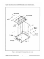
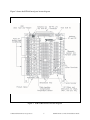
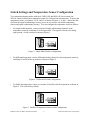
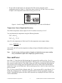
NATIONAL
INSTRUMENTS
®
The Software is the Instrument
®
SCB-68 68-Pin Shielded
Connector Block
Installation Guide
Part Number 320745-01
This guide describes how to connect and use the SCB-68 68-pin shielded connector block with
National Instruments 68-pin products. In addition to the SCB-68 kit contents, you need Phillipshead number 1 and number 2 screwdrivers, a 0.125 in. flathead screwdriver, long-nose pliers,
wire cutters, and wire insulation strippers. If you are adding components, you also need a
soldering iron and solder, and resistors and capacitors (specific to your application).
Introduction
The SCB-68 is a shielded board with 68 screw terminals for easy connection to National
Instruments 68-pin products.
When you use the SCB-68 with the AT-MIO-16X or MIO-16E Series boards, you can use the
16 screw terminals for signal connection to the 16 analog inputs. There is a breadboard area for
adding resistance-capacitance (RC) filtering, an attenuator, 4 to 20 mA current sensing, and open
thermocouple detection. There is also a cold-junction temperature sensor for use with
thermocouples.
When you are using an unmodified SCB-68 with other 68-pin products, you can configure the
five switches to give you a general-purpose 68-screw terminal connector block. The SCB-68 has
a strain-relief bar for securing signal wires or cables.
What Your Kit Should Contain
The SCB-68 68-pin shielded connector block kit (part number 776844-01) contains the following
components:
Kit Component
Part Number
SCB-68 68-pin shielded connector block
SCB-68 Quick Reference Label
SCB-68 68-Pin Shielded Connector Block Installation Guide
182470-01
182509-01
320745-01
If your kit is missing any components, contact National Instruments.
Figure 1 shows how to remove the SCB-68 shielded connector block from its box.
_____________________________
Product and company names are trademarks or trade names of their respective companies.
© 1994 National Instruments Corporation. All rights reserved.
January 1994
Figure 2 shows the SCB-68 board parts locator diagram.
Figure 2. SCB-68 Board Parts Locator Diagram
© National Instruments Corporation
3
SCB-68 Connector Block Installation Guide
Switch Settings and Temperature Sensor Configuration
To accommodate thermocouples with the AT-MIO-16X and MIO-16E Series boards, the
SCB-68 connector block has a temperature sensor for cold-junction compensation. To power the
temperature sensor, set switches S1, S2, and S3 as shown in Figures 3, 4, and 5. Notice that this
also turns the signal conditioning accessory power on (accessories can include temperature
sensors and signal conditioning circuitry). You can configure the temperature sensor as follows:
•
For single-ended operation, connect referenced single-ended analog channel 0 to the
temperature sensor by switching S5 to the up position. The signal is referenced to analog
input ground. Set the switches as shown in Figure 3.
S1
S2
S5 S4 S3
Figure 3. Single-Ended Switch Configuration
•
For differential operation, connect differential analog channel 0 to the temperature sensor by
switching S5 and S4 to the up position, as shown in Figure 4.
S1
S2
S5 S4 S3
Figure 4. Differential Switch Configuration
•
To disable the temperature sensor, set switches S5 and S4 in the down position, as shown in
Figure 5. This is the factory default.
S1
S2
S5 S4 S3
Figure 5. Disabled Temperature Sensor Switch Configuration
SCB-68 Connector Block Installation Guide
4
© National Instruments Corporation
•
For use with a 68-pin board, you can bypass all of the circuitry using the switch
configuration shown in Figure 6. Notice that when switches S1, S2, and S3 are set as shown
in Figure 6, the temperature sensor and accessory power are off.
S1
S2
S5 S4 S3
Figure 6. Switch Configuration for General-Purpose Use with a 68-Pin Board
Temperature Sensor Output and Accuracy
The SCB-68 temperature sensor outputs 10 mV/°C and has an accuracy of ±1° C.
You can determine the temperature using the following formulas:
T(°C) =100 x V t
T(°C) = TK - 273.15
where TK is the temperature in Kelvin and Vt is the temperature sensor output voltage.
T(° F) =
[T(°C)] 9 + 32
5
where T(°F) and T(°C) are the temperature readings in degrees Fahrenheit and degrees Celsius,
respectively.
Note:
Use the average of a large number of samples to obtain the most accurate reading.
Noisy environments require more samples for greater accuracy.
Fuse and Power
One of the +5 V lines from the DAQ board (pin 8) is protected by an 800 mA fuse. Pin 14 is
also +5 V and is not fuse protected on the SCB-68. Shorting pin 14 to ground will blow the MIO
fuse, which is usually socketed. If the SBC-68 does not work when you turn the DAQ board on,
first check the switch settings, then check both the 800 mA fuse on the SCB-68 board and the
output fuse (if any) on the DAQ board. Before replacing any fuses, check for short circuits from
power to ground.
The 5 V power on the SCB-68 is filtered with a 470 Ω series resistor (R21); as the filtered 5 V is
loaded, the voltage decreases. Pad R20 is in parallel with R21 and you can install a resistor if
needed. Shorting R20 bypasses the filter while capacitatively coupling DGND and AGND, and
is not recommended.
© National Instruments Corporation
5
SCB-68 Connector Block Installation Guide
Quick Reference Label
A quick reference label is in your kit for your convenience. This label shows the switch
configurations and defines the screw terminal pinouts for the AT-MIO-16X and MIO-16E Series
boards. You can put the label on the inside of the SCB-68 cover for easy reference.
Signal Connection
The following warnings contain important safety information concerning hazardous voltages and
terminal blocks.
Warnings:
KEEP AWAY FROM LIVE CIRCUITS. Do not remove equipment covers or shields
unless you are trained to do so. If signal wires are connected to the module or
terminal block, dangerous voltages may exist even when the equipment is
turned off. To avoid dangerous electrical shock, do not perform procedures
involving cover or shield removal unless you are qualified to do so. Before you
remove the cover, disconnect the AC power or any live circuit from the terminal
block.
The chassis GND terminals on your terminal block are for grounding highimpedance sources such as a floating source (1 mA maximum). Do NOT use
these terminals as safety earth grounds.
Do not connect high voltages to the SCB-68 even with an attenuator circuit.
Never connect voltages ≥42 Vrms. National Instruments is NOT liable for any
damages or injuries resulting from improper use or connection.
To connect the signal to the terminal block, perform the following steps:
1. Disconnect the 68-pin cable from the SCB-68 if it is connected.
2. Remove the shielding screws on either side of the top cover with a Phillips-head number 1
screwdriver (see Figure 1). You can now open the box.
3. Configure the switches and other options relative to the types of signals you are using as
explained in the Switch Settings and Temperature Sensor Configuration section of this guide.
4. Loosen the strain-relief screws with a Phillips-head number 2 screwdriver. Slide the signal
wires through the front panel strain-relief opening. You can also remove the top strain-relief
bar if you are connecting many signals. Add insulation or padding if necessary.
5. Connect the wires to the screw terminals by stripping off 0.25 in. of the insulation, inserting
the wires into the green terminals, and tightening the screws.
6. Reinstall the strain-relief bar (if you removed it) and tighten the strain-relief screws.
7. Close the top cover.
8. Reinsert the shielding screws to ensure proper shielding.
You can now connect the terminal block to the 68-pin connector.
SCB-68 Connector Block Installation Guide
6
© National Instruments Corporation
Removing the SCB-68 Board
To solder components in place, you can remove the SCB-68 board using the following steps:
1. Disconnect the 68-pin cable from the SCB-68 if it is connected.
2. Remove the shielding screws on either side of the top cover with a Phillips-head number 1
screwdriver. You can now open the box.
3. Loosen the strain-relief screws with a Phillips-head number 2 screwdriver.
4. Remove the signal wires from screw terminals.
5. Remove the board mount screws and the 68-pin connector screws.
6. Tilt the board up and pull it out.
To reinstall the SCB-68 board, reverse the order of the steps.
Application Notes
When you use the SCB-68 with the AT-MIO-16X or MIO-16E Series boards, you can use the
16 screw terminals for signal connection to the 16 analog inputs. There is a breadboard area for
these inputs to allow RC filtering, 4 to 20 mA current sensing, open thermocouple detection, and
an attenuator. There are also pads for DAC0OUT, DAC1OUT, and EXTTRIG to permit RC
filtering and an attenuator. The open component positions on the SCB-68 board make adding
signal conditioning components to the analog input signals easier. Figure 7 shows an example
for a specific input channel, and all of the channels are arranged the same way.
Soldering and Desoldering on the SCB-68 Board
Some applications discussed here require you to make modifications to the printed circuit board,
usually in the form of adding components. The SCB-68 board is shipped with wire jumpers in
the F and G positions (see Figure 7); you must remove them to use the positions. Use a lowwattage soldering iron (20 to 30 W) when soldering to the board. To desolder on the SCB-68,
vacuum-type tools work best. Be careful to avoid damaging the component pads when
desoldering. Use only rosin-core electronic grade solder, because acid-core solder damages the
printed circuit board and components.
ACH0+
+5V
R22(A)
RC12(B)
R4(F)
68
RC4(E)
R23(C)
34
R5(G)
RC13(D)
AIGND
ACH8+ or ACH0-
Figure 7. Channel Configuration Diagram
© National Instruments Corporation
7
SCB-68 Connector Block Installation Guide
Channel Configurations
You can configure the analog input channels of an MIO-16 board for one of three input modes–
differential, referenced single-ended, or nonreferenced single-ended. These modes are called
DIFF, RSE, and NRSE input modes, respectively.
As described in your MIO-16 user manual, the input configuration of the MIO-16 board depends
on the type of signal source you are using. There are two types of signal sources–nonreferenced
or floating signals, and ground-referenced signals. To measure floating signal sources, configure
the MIO-16 for referenced single-ended input or differential input with bias resistors. To
measure ground-referenced signal sources, configure the MIO-16 for nonreferenced single-ended
input or differential input. Both types of signal sources and the recommended methods for
MIO-16 board connection are discussed as follows.
Connecting Nonreferenced or Floating Signal Sources
A floating signal source is a signal source that is not connected in any way to the building ground
system, but has an isolated ground-reference point. If an instrument or device has an isolated
output, that instrument or device falls into the floating signal source category. Some examples of
floating signal sources are outputs for thermocouples, transformers, battery-powered devices,
optical isolators, and isolation amplifiers. The ground reference of a floating source must be tied
to the ground of the DAQ board to establish a local or onboard reference for the signal.
Differential Inputs
To provide a return path for the instrumentation amplifier bias currents, floating sources must
have a 10 to 100 kΩ resistor to AIGND on one input if they are DC-coupled, or on both inputs if
sources are AC-coupled. You can install bias resistors in positions B and D (see Figure 7) of the
SCB-68. For more detailed information on connections to floating signal sources and differential
inputs, refer to the configuration chapter in your MIO-16 board user manual.
Single-Ended Inputs
When measuring floating signal sources, configure your MIO-16 board to supply a ground
reference. Therefore, you should configure the MIO-16 for referenced single-ended input. In
this configuration, the negative input of the MIO-16 instrumentation amplifier is tied to the
analog ground. Therefore, you should use the SCB-68 board in its factory configuration. In the
factory configuration, jumpers are in the two series positions, F and G (see Figure 7). In this
configuration, you should tie all of the signal grounds to AIGND.
Connecting Ground-Referenced Signal Sources
A grounded signal source is connected in some way to the building system ground; therefore, the
signal source is already connected to a common ground point with respect to the DAQ board
(assuming that the host computer is plugged into the same power system). Nonisolated outputs
of instruments and devices that plug into the building power system fall into this category.
SCB-68 Connector Block Installation Guide
8
© National Instruments Corporation
Differential Inputs
If the MIO-16 DAQ board is configured for differential inputs, ground-referenced signal sources
connected to the SCB-68 board need no special components. You can leave the inputs of the
SCB-68 board in the factory configuration, that is, with the jumpers in the two series positions,
F and G (see Figure 7).
Single-Ended Inputs
When you measure ground-referenced signals, the external signal supplies its own reference
ground point, and the MIO-16 should not supply one. Therefore, you should configure the
MIO-16 board for nonreferenced single-ended input mode. In this configuration, tie all of the
signal grounds to AISENSE, which connects to the negative input of the instrumentation
amplifier on the MIO-16 board.
You can leave the SCB-68 inputs in the factory configuration, that is, with jumpers in the series
position (F or G, depending on the channel). Do not use the open positions that connect the input
to AIGND, A and C (see Figure 7), in this configuration. Therefore, you should build signal
conditioning circuitry requiring a ground reference in the custom breadboard area using
AISENSE as the ground reference instead of building the circuitry in the open component
positions. Referencing the signal to AIGND can cause inaccurate measurements resulting from
an incorrect ground reference.
Building RC Filters
You can connect RC filters, which can reduce noise, to the SCB-68 analog inputs. You can build
single or differential RC filters using the pads on the SCB-68. Filtering increases settling time to
the time constant of the filter you use.
Adding RC filters to scanning channels greatly reduces the scanning rate; settling times can be
10 T (T = RC) or longer. Refer to Application Note 043, Measuring Temperature with
Thermocouples (National Instruments part number 340524-01) to determine if the settling time
will affect your signal measurements.
Single-Ended RC Filters
You can build single RC filters using the pads F and B for one channel and G and D for the next
channel. Solder the resistor in position F or G and the capacitor in position B or D. The
following equation shows how to determine your cutoff frequency (Fc ) and settling time
depending on the resistors and capacitators you use.
Fc = 1/(2 πRC)
Differential RC Filters
You can build a differential RC filter using the pads F and E. Solder the resistor in position F
and the capacitor in position E. The following equation shows how to determine your cutoff
frequency (Fc ) and settling time depending on the resistors and capacitators you use.
Fc = 1/(2 πRC)
© National Instruments Corporation
9
SCB-68 Connector Block Installation Guide
Using 4 to 20 mA Inputs
You can connect a resistor to the analog inputs at the SCB-68 board for use with current sourcing
devices. You can perform single-ended or differential sensing using the SCB-68 pads. Accuracy
depends on the resistor you use. Never exceed ±10 V at the analog inputs.
Single-Ended Inputs
Use position B for one channel and position C for the next channel. Leave the jumpers in place
for each channel, position F for one and position G for the next .
Differential Inputs
Use position E for each channel you are using for current sensing. Leave the jumpers in
positions F and G for each channel.
Building Attenuators (Voltage Dividers)
You can connect attenuators (voltage dividers) to the SCB-68 analog inputs. Attenuators can
reduce a signal that is outside the normal input range of the DAQ board (±10 V maximum).
Warning:
The SCB-68 board is not designed for any input voltages greater than 42 V, even
if a user-installed voltage divider reduces the voltage to within the input range of
the DAQ board. Input voltages greater than 42 V can damage the SCB-68 board,
any and all boards connected to it, and the host computer. Overvoltage can also
cause an electric shock hazard for the operator. National Instruments is NOT
liable for damage or injury resulting from such misuse.
Single-Ended Input Attenuators
There is a two-resistor circuit for attenuating voltages at the single-ended inputs on the SCB-68.
Install resistors in positions F and B for one channel and G and C for the next channel.
You can determine the gain (G) of this attenuator using the following formula:
G = Rb/(Rb + Rf) or G = Rg/(Rg + Rc)
Therefore, the input to the MIO-16 board (VMIO) is computed as follows:
VMIO = VSC * G
where VSC is the voltage applied to the SCB-68 screw terminals. The accuracy of this gain
equation depends on the tolerances of the resistors you use.
Differential Input Attenuators
There is a three-resistor circuit for attenuating voltages at the differential inputs on the SCB-68.
Use positions E, F, and G for the resistors.
SCB-68 Connector Block Installation Guide
10
© National Instruments Corporation
Use the following equation to determine the sources of error:
G = Re/(Re + Rf + Rg)
Therefore, the input to the MIO-16 board (VMIO) is computed as follows:
VMIO = VSC * G
where VSC is the voltage applied to the SCB-68 screw terminals. The accuracy of this gain
equation depends on the tolerances of the resistors you use.
Using the SCB-68 Board for Thermocouple Measurements
The maximum voltage level thermocouples generate is typically a few millivolts. Therefore, you
should use an MIO-16 with high gain for best resolution. You can measure thermocouples in
either differential or single-ended configurations. The differential configuration has better noise
immunity, but the single-ended configuration has twice as many inputs. The MIO-16 board must
have a ground reference because thermocouples are floating signal sources. Therefore, you must
use bias resistors if the board is in differential mode. For single-ended configuration, use the
referenced single-ended input configuration.
Cold-junction compensation with the SCB-68 board is accurate only if the temperature sensor
reading is close to the actual temperature of the screw terminals. When you are reading
thermocouple measurements, keep the SCB-68 board away from drafts or other temperature
gradients such as those caused by heaters, radiators, fans, and very warm equipment.
Input Filtering and Open Thermocouple Detection (Optional)
To reduce noise, you can connect a lowpass filter. Refer to the Building RC Filters section
earlier in this guide.
Build open thermocouple detection circuitry by connecting a high-value resistor between the
positive input and +5 V. The value of this resistor is relatively unimportant; a few megohms or
more works fine. With a high-value resistor, you can detect an open or defective thermocouple.
If the thermocouple opens, the voltage measured across the input terminals rises to +5 V, a value
much larger than any legitimate thermocouple voltage. The 100 kΩ resistor between the
negative input and AIGND is a bias current return path as described in the Connecting Floating
Signal Sources section earlier in this guide.
Differential Open Thermocouple Detection
Use position A to connect a high-value resistor between the positive input and +5 V. Leave the
jumpers in place (positions F and G) for each channel used.
Single-Ended Open Thermocouple Detection
Use position A for one channel and D for the next channel when you connect a high-value
resistor between the positive input and +5 V. Leave the jumpers in place for each channel,
position F for one channel and G for the next channel.
© National Instruments Corporation
11
SCB-68 Connector Block Installation Guide
RC Filters and Attenuators for DAC0OUT, DAC1OUT, and EXTTRIG
You can connect RC filters and attenuators to the DAC0OUT, DAC1OUT, and EXTTRIG
signals at the SCB-68 board. RC filters can reduce noise. You can build these using the SCB-68
pads. Filtering increases settling time to the time constant of the filter you use.
RC Filters
You can build single RC filters using the pads R1 and RC1 for EXTTRIG, R2 and RC2 for
DAC1OUT, and R3 and RC3 for DAC0OUT. Solder the resistor in position R1, R2, or R3, and
the capacitor in position RC1, RC2, or RC3. Determine your cutoff frequency and settling time
using the following formulas:
Fc = 1/(2 πRC)
Settling time = 9 T for 12-bit DACs
12 T for 12-bit DACs
Attenuators
You can connect attenuators (voltage dividers) to the SCB-68 board. Attenuators can reduce a
signal that is outside the normal input range of the DAQ board (±10 V maximum).
There is a two-resistor circuit for attenuating voltages on the SCB-68 at DAC0OUT, DAC1OUT,
and EXTTRIG. Use pads R1 and RC1 for EXTTRIG, R2 and RC2 for DAC1OUT, and R3 and
RC3 for DAC0OUT for the resistors.
You can determine the gain (G) of this attenuator using the following formula:
G = RC1/(RC1 + R1) or G = RC2/(RC2 + R2) or G = RC3/(RC3 + R3)
Warning:
The SCB-68 board is not designed for any input voltages greater than 42 V, even
if a user-installed voltage divider reduces the voltage to within the input range of
the DAQ board. Input voltages greater than 42 V can damage the SCB-68 board,
any and all boards connected to it, and the host computer. Overvoltage can also
cause an electric shock hazard for the operator. National Instruments is NOT
liable for damage or injury resulting from such misuse.
Sources of Error
When making thermocouple measurements with the SCB-68 board and an MIO-16 board, the
possible sources of error are compensation, linearization, measurement, and thermocouple wire
errors.
Compensation error can arise from two sources–inaccuracy of the temperature sensor, and
temperature differences between the sensor and the screw terminals. The sensor on the SCB-68
board is specified to be accurate to ±1° C. You can minimize temperature differences between
the sensor and the screw terminals by keeping the SCB-68 board away from drafts, heaters, and
warm equipment.
SCB-68 Connector Block Installation Guide
12
© National Instruments Corporation
Thermocouple output voltages are nonlinear with respect to temperature. Conversion of the
voltage output to temperature using either look-up tables or polynomial approximations
introduces linearization error. The linearization error is dependent on how closely the table or
the polynomial approximates the true thermocouple output. For example, you can reduce your
linearization error by using a higher degree polynomial.
Measurement error is the result of inaccuracies in the plug-in board. These inaccuracies include
gain and offset. If the board is properly calibrated, the offset error should be zeroed out. The
only remaining error is a gain error of ±0.08% of full range (see the MIO-16 specifications). If
the input range is ±10 V and the gain is 500, gain error contributes 0.0008 x 20 mV, or 16 µV of
error. If the Seebeck coefficient of a thermocouple is 32 µV/°C, this measurement error adds
0.5° C of uncertainty to the measurement. For best results, you must use a well-calibrated
MIO-16 board so that offsets can be ignored. You can eliminate offset error, however, by
grounding one channel on the SCB-68 board and measuring the voltage. You can then subtract
this value, the offset of the MIO-16, in software from all other readings.
Thermocouple wire error is the result of inconsistencies in the thermocouple manufacturing
process. These inconsistencies, or nonhomogeneities, are the result of defects or impurities in
the thermocouple wire. The errors vary widely depending on the thermocouple type and even
the gauge of wire used, but a value of ±2° C is typical. For more information on thermocouple
wire errors and more specific data, consult your thermocouple manufacturer.
For best results, use the average of many readings (about 100 or so); typical absolute accuracies
should then be about ±2° C.
Specifications
This section lists the SCB-68 specifications. These ratings are typical at 25° C unless otherwise
stated. The operating temperature range for this board is 0° to 70° C.
Analog Input
Number of channels
Cold-junction sensor
Accuracy
Output
Other signals
Eight differential, 16 single-ended
±1.0° C over a 0° to 110° C range
10 mV/°C
All other MIO-16 I/O signals are available at
screw terminals
Power Requirement
Power consumption (at +5 VDC ±5%)
Typical
Maximum
1 mA with no signal conditioning installed
800 mA from host computer
Note: The power specifications pertain to the power supply of the host computer when using
internal power or to the external supply connected at the +5 V screw terminal when
using external power. The maximum power consumption of the SCB-68 is a function
of the signal conditioning components installed and any circuits constructed on the
general-purpose breadboard area. If the SCB-68 is being powered from the host
computer, the maximum +5 V current draw is fuse-limited to 800 mA.
© National Instruments Corporation
13
SCB-68 Connector Block Installation Guide
Physical
Box dimensions (including box feet)
I/O connectors
Screw terminals
7.7 by 6.0 by 1.8 in. (19.5 by 15.2 by 4.5 cm )
One 68-pin male SCSI connector
68
Operating Environment
Temperature
Relative humidity
0° to 70° C
5% to 90% noncondensing
Storage Environment
Temperature
Relative humidity
SCB-68 Connector Block Installation Guide
-55° to 125° C
5% to 90% noncondensing
14
© National Instruments Corporation