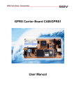
1
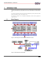
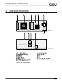
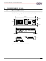
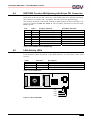
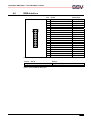
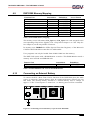
DIL/NetPC DNP/5280
Board Revision 1.2
Hardware Reference
SSV Embedded Systems
Heisterbergallee 72
D-30453 Hannover
Phone +49-(0)511-40000-0
Fax
+49-(0)511-40000-40
E-mail: [email protected]
For further information regarding our products please visit us at www.dilnetpc.com
Manual Revision: 1.0
Date: 2004-08-30
DIL/NetPC DNP/5280 – Content
CONTENT
1
INTRODUCTION ................................................................................................. 3
1.1
1.2
Block Diagram ......................................................................................................... 3
Features ................................................................................................................... 4
2
DNP/5280 OVERVIEW ........................................................................................ 5
3
DNP/5280 COMPONENTS .................................................................................. 6
3.1
3.2
3.3
3.4
3.5
3.6
3.7
3.8
3.9
3.10
3.11
4
J1 – BDM Interface .................................................................................................. 6
MCF5282CVF66 CPU.............................................................................................. 6
SDRAM ................................................................................................................... 6
32KHz Quartz .......................................................................................................... 6
Flash Memory .......................................................................................................... 6
10/100 Mbps Ethernet PHY ...................................................................................... 6
LAN Activity LEDs ................................................................................................. 6
RTC DS1306............................................................................................................ 7
TTL ......................................................................................................................... 7
TTL ......................................................................................................................... 7
J2 – 64-pin DIL Connector ....................................................................................... 7
THE DNP/5280 IN DETAIL .................................................................................. 8
4.1
4.2
4.3
4.4
4.5
4.6
4.7
4.8
4.9
4.10
Mechanical Dimensions ........................................................................................... 8
Pin Assignment – 64-pin DIL Connector (1. Part) ..................................................... 9
Pin Assignment – 64-pin DIL Connector (2. Part) ................................................... 10
DNP/5280 Function Multiplexing with 64-pin DIL Connector ................................ 11
LAN Activity LEDs ............................................................................................... 11
BDM-Interface....................................................................................................... 12
PIO-Mapping ......................................................................................................... 13
DNP/5280 Expansion Bus Mapping ........................................................................ 14
DNP/5280 Memory Mapping.................................................................................. 15
Connecting an External Battery .............................................................................. 15
CONTACT .............................................................................................................. 16
DOCUMENT HISTORY ........................................................................................... 16
SSV EMBEDDED SYSTEMS
2
DIL/NetPC DNP/5280 – Introduction
1
INTRODUCTION
Thank you for choosing a SSV Product. We are confident that you will be pleased
with the performance of your product. Please take a few minutes to read this manual.
For further information about the individual components you may follow the links
from our website at: http://www.dilnetpc.com
Our Website contains a lot of technical information, which will be updated in
regular periods.
1.1
Block Diagram
Figure 1-1: Block Diagram of the MCF5280/MCF5282-Microcontroller
Figure 1-2: Block Diagram of the DNP/5280
SSV EMBEDDED SYSTEMS
3
DIL/NetPC DNP/5280 – Introduction
1.2
Features
•
Motorola 32-bit MCF5282 ColdFire with 66 MHz Clock Speed
•
63 MIPS (Dhrystone 2.1)
•
16 MByte SDRAM Memory, 8 MByte FLASH Memory
•
10/100 Mbps Ethernet LAN Interface
•
Four LAN Status LEDs
•
Two asynchronous Serial Ports (one with all Handshakes)
•
One I2C Interchip Bus Interface
•
One Queued Serial Peripheral Interface (SPI)
•
One CAN Interface (Supports CAN Protocol Specification 2.0B)
•
20-bit General Purpose high-speed Parallel I/O
•
8-bit I/O Expansion Bus
•
Five Interrupt Inputs
•
Four Chip Select Outputs
•
Programmable General Purpose Timers and Watchdog Timer
•
Motorola BDM (Background Debug Mode) Interface for In-Circuit Debugging
•
In-System Programming Features
•
64-pin JEDEC DIL-64 Connector, 2.54mm Centers
•
3.3 Volt Low Power Design, Supply Voltage 3.3 VDC (± 5%)
•
Supply Current 300 mA typ. at 66 MHz
•
Size 82mm x 28mm
SSV EMBEDDED SYSTEMS
4
DIL/NetPC DNP/5280 – DNP/5280 Overview
2
DNP/5280 OVERVIEW
1 2 3 4
1
DIL/NetPC DNP/5280
top view
1
DIL/NetPC DNP/5280
bottom view
Figure 2-1: OverviewDNP/5280
SSV EMBEDDED SYSTEMS
5
DIL/NetPC DNP/5280 – DNP/5280 Components
3
DNP/5280 COMPONENTS
This chapter describes components of the DIL/NetPC DNP/5280 shown in chapter 2 and gives a short overview about their respective functions.
3.1
J1 – BDM Interface
The BDM (Background Debug Mode) interface offers in-circuit debugging.
Through a special adapter cable the Flash memory is in-system programmable.
Please refer to chapter 4.6 for the complete pinout.
3.2
MCF5282CVF66 CPU
The DNP/5280 provides a very compact ColdFire-based low power embedded
controller (Motorola 32-bit MCF5282CVF66) with TCP/IP stack and web server
for high-speed embedded networking applications.
3.3
SDRAM
The capacity of the SDRAM memory chip is 16 MByte with a 32-bit data path.
3.4
32KHz Quartz
This 32KHz quartz is used by the RTC (real time clock).
3.5
Flash Memory
The boot block of the Flash memory is only in-system programmable over the
Motorola BDM interface through a special adapter cable attached to a PC parallel
port. For all other Flash blocks you can use also a high-speed serial connection
through the DNP/5280 COM1 port or the 10/100 Mbps Ethernet interface for insystem programming.
3.6
10/100 Mbps Ethernet PHY
The DNP/5280 is using a Realtek RTL8201BL PHY 10/100Mbps chip that allows
Ethernet connectivity with a speed up to 100Mbps. The RJ45 Ethernet interface
on the Evaluation Board is just a simple connection over a transformer to the DIL
interface pins, which are connected to the LAN controller onto the DNP/5280.
3.7
LAN Activity LEDs
These four miniature LEDs are placed on the DNP/5280 for a visual check of the
LAN activity. Please refer to chapter 4.5 for detailed information.
SSV EMBEDDED SYSTEMS
6
DIL/NetPC DNP/5280 – DNP/5280 Components
3.8
RTC DS1306
Real time clock circuit.
3.9
TTL
The 74AHC138 circuit is used for generating external chip selects.
3.10
TTL
The 74LVC541 circuit is used for the reset configuration of the Coldfire CPU.
3.11
J2 – 64-pin DIL Connector
The mechanical interface between the DNP/5280 and existing devices and equipment is a JEDEC 64-pin DIL connector with 2.54mm centers. This allows the direct integration to a standard 64-pin DIL socket.
Please refer to chapter 4.2 and 4.3 for the complete pinout.
SSV EMBEDDED SYSTEMS
7
DIL/NetPC DNP/5280 – The DNP/5280 in Detail
4
THE DNP/5280 IN DETAIL
4.1
Mechanical Dimensions
The DNP/5280 uses a 64-pin DIL socket as mechanical base. Figure 4-1 shows the
dimensions. All length dimensions have a tolerance of 0.5 mm.
82 mm
2,52 mm
28 mm
1 2 3 4
1
2,62 mm
2,54 mm
78,74 mm
1,6 mm
1,65 mm
6 mm
15 mm
22,86 mm
2,52 mm
2,62 mm
Figure 4-1: Mechanical dimensions of the DNP/5280
SSV EMBEDDED SYSTEMS
8
DIL/NetPC DNP/5280 – The DNP/5280 in Detail
4.2
Pin Assignment – 64-pin DIL Connector (1. Part)
Pin
1
2
3
4
5
6
7
8
9
10
11
12
13
14
15
16
17
18
19
20
21
22
23
24
25
26
27
28
29
30
31
32
Name
PA0
PA1
PA2
PA3
PA4
PA5
PA6
PA7
PB0
PB1
PB2
PB3
PB4
PB5
PB6
PB7
PC0
PC1
PC2
PC3
RXD1
TXD1
CTS1
RTS1
DCD1
DSR1
DTR1
RI1
RESIN
TX+
TXGND
Group
PIO
PIO
PIO
PIO
PIO
PIO
PIO
PIO
PIO
PIO
PIO
PIO
PIO
PIO
PIO
PIO
PIO
PIO
PIO
PIO
SIO
SIO
SIO
SIO
SIO
SIO
SIO
SIO
RESET
LAN
LAN
----
Function
Parallel I/O, Port A, Bit 0
Parallel I/O, Port A, Bit 1
Parallel I/O, Port A, Bit 2
Parallel I/O, Port A, Bit 3
Parallel I/O, Port A, Bit 4
Parallel I/O, Port A, Bit 5
Parallel I/O, Port A, Bit 6
Parallel I/O, Port A, Bit 7
Parallel I/O, Port B, Bit 0
Parallel I/O, Port B, Bit 1
Parallel I/O, Port B, Bit 2
Parallel I/O, Port B, Bit 3
Parallel I/O, Port B, Bit 4
Parallel I/O, Port B, Bit 5
Parallel I/O, Port B, Bit 6
Parallel I/O, Port B, Bit 7
Parallel I/O, Port C, Bit 0
Parallel I/O, Port C, Bit 1
Parallel I/O, Port C, Bit 2
Parallel I/O, Port C, Bit 3
COM1 Serial Port, RXD Pin
COM1 Serial Port, TXD Pin
COM1 Serial Port, CTS Pin
COM1 Serial Port, RTS Pin
COM1 Serial Port, DCD Pin
COM1 Serial Port, DSR Pin
COM1 Serial Port, DTR Pin
COM1 Serial Port, RI Pin
Reset Input
10/100 Mbps LAN, TX+ Pin
10/100 Mbps LAN, TX- Pin
Ground
Table 4-1: DNP/5280 Pinout – Pin 1 to 32
SSV EMBEDDED SYSTEMS
9
DIL/NetPC DNP/5280 – The DNP/5280 in Detail
4.3
Pin Assignment – 64-pin DIL Connector (2. Part)
Pin
33
34
35
36
37
38
39
40
41
42
43
44
45
46
47
48
49
50
51
52
53
54
55
56
57
58
59
60
61
62
63
64
Name
RX+
RXRESOUT
VBAT
CLKOUT
TXD2
RXD2
INT5
INT4
INT3
INT2
INT1
CS4
CS3
CS2
CS1
IOCHRDY
IOR
IOW
SA3
SA2
SA1
SA0
SD7
SD6
SD5
SD4
SD3
SD2
SD1
SD0
Vcc
Group
LAN
LAN
RESET
PSP
PSP
PSP
PSP
PSP
PSP
PSP
PSP
PSP
PSP
PSP
PSP
PSP
PSP
PSP
PSP
PSP
PSP
PSP
PSP
PSP
PSP
PSP
PSP
PSP
PSP
PSP
PSP
PSP
Function
10/100 Mbps LAN, RX+ Pin
10/100 Mbps LAN, RX- Pin
Reset Output
Real-Time Clock Battery
Clock Output
COM2 Serial Port, TXD Pin
COM2 Serial Port, RXD Pin
Interrupt Input 5
Interrupt Input 4
Interrupt Input 3
Interrupt Input 2
Interrupt Input 1
Chip Select Output 4
Chip Select Output 3
Chip Select Output 2
Chip Select Output 1
I/O Channel Ready
I/O Read Signal
I/O Write Signal
Address Bit 3
Address Bit 2
Address Bit 1
Address Bit 0
Data Bit 7
Data Bit 6
Data Bit 5
Data Bit 4
Data Bit 3
Data Bit 2
Data Bit 1
Data Bit 0
3.3 Volt Power Input
Table 4-2: DNP/5280 Pinout – Pin 33 to 64
SSV EMBEDDED SYSTEMS
10
DIL/NetPC DNP/5280 – The DNP/5280 in Detail
4.4
DNP/5280 Function Multiplexing with 64-pin DIL Connector
Some pins of the 64-pin DIL connector of the DNP/5280 have multiple meanings.
The pins have a primary and a secondary function (Function Multiplexing).
The primary functions correspond with the standard pinout of the 64-pin DIL connec-tor as shown in table 4-1 and 4-2. The secondary functions are shown in table 4-3 below.
Pin
13
14
15
16
17
18
19
20
Name
PB4
PB5
PB6
PB7
PC0
PC1
PC2
PC3
Primary functions
Parallel I/O, Port B, Bit 4
Parallel I/O, Port B, Bit 5
Parallel I/O, Port B, Bit 6
Parallel I/O, Port B, Bit 7
Parallel I/O, Port C, Bit 0
Parallel I/O, Port C, Bit 1
Parallel I/O, Port C, Bit 2
Parallel I/O, Port C, Bit 3
Secondary functions
SCL (I2C)
SDA (I2C)
CANTX (CAN)
CANRX (CAN)
QSPIDO (SPI)
QSPIDI (SPI)
QSPICLK (SPI)
QSPICS0 (SPI)
Table 4-3: DNP/5280 Function Multiplexing
4.5
LAN Activity LEDs
Four miniature LEDs are placed on the DNP/5280 for a visual check of the LAN
activity.
Name
LED 1
LED 2
LED 3
LED 4
Function
Link
Duplex
10Act
100Act
Description
Ethernet cable plugged in
Duplex-Mode
Data transmission with 10 Mbps
Data transmission with 100 Mbps
Table 4-4: DNP/5280 LEDs
1 2 3 4
1
DIL/NetPC DNP/5280
LED 1
LED 2
LED 3
LED 4
Figure 4-2: DNP/5280 LEDs
SSV EMBEDDED SYSTEMS
11
DIL/NetPC DNP/5280 – The DNP/5280 in Detail
4.6
BDM-Interface
Pin
1
2
3
4
5
6
7
8
9
10
11
12
13
14
15
16
17
18
19
20
Name
VIO (3.3 VDC I/O Voltage)
GND
TA#
BKPT#
Reset#
DSCLK#
DSI#
TCLK
PST3
DS0
PST2
DDATA3
PST1
DDATA2
PST0
DDATA1
PSTCLK
DDATA0
GND
RCM
Annotation
Power
Ground
BDM-Function
BDM-Function
BDM-Function
BDM-Function
BDM-Function
BDM-Function
BDM-Function
BDM-Function
BDM-Function
BDM-Function
BDM-Function
BDM-Function
BDM-Function
BDM-Function
BDM-Function
BDM-Function
Ground
GPTB3
Table 4-5: DNP/5280 BDM-Interface
Pin 19 – Pin 20
Jumper not set
Jumper set
Effects
GPTB3 = 1 (High)
GPTB3 = 0 (Low)
Table 4-6: DNP/5280 RCM-Jumper
SSV EMBEDDED SYSTEMS
12
DIL/NetPC DNP/5280 – The DNP/5280 in Detail
4.7
PIO-Mapping
The 20 Signals for the DNP/5280-Parallel-I/O (PIO) are realized through different
function units of the MCF5280. The following table shows the assignment. Pin
names for the MCF5280-case (256 MAPBGA) are listed in the third column.
Please see the MCF5282 ColdFire Microcontroller User’s Manual R.0.1
(MCF5282UM/D) for further details.
Pin
1
2
3
4
5
6
7
8
9
10
11
12
13
14
15
16
17
18
19
20
Name
PA0
PA1
PA2
PA3
PA4
PA5
PA6
PA7
PB0
PB1
PB2
PB3
PB4
PB5
PB6
PB7
PC0
PC1
PC2
PC3
MCF5280-Pinfunction
AN52
AN53
AN55
AN56
AN0
AN1
AN2
AN3
GPTA0
GPTA1
GPTA2
GPTA3
SCL
SDA
CANTX
CANRX
QSPIDO
QSPIDI
QSPICLK
QSPICS0
MCF5280-Pin
R4
T4
P3
R3
T3
R2
T2
R1
N13
P13
R13
T13
E15
E14
E13
D16
F13
E16
F14
F15
Table 4-7: DNP/5280 PIO-Mapping
SSV EMBEDDED SYSTEMS
13
DIL/NetPC DNP/5280 – The DNP/5280 in Detail
4.8
DNP/5280 Expansion Bus Mapping
Pin
40
41
42
43
44
45
46
47
48
49
50
51
52
53
54
55
56
57
58
59
60
61
62
63
Name
INT5
INT4
INT3
INT2
INT1
CS4
CS3
CS2
CS1
RDY
RD
WR
SA3
SA2
SA1
SA0
SD7
SD6
SD5
SD4
SD3
SD2
SD1
SD0
Function
Interrupt Input 5
Interrupt Input 4
Interrupt Input 3
Interrupt Input 2
Interrupt Input 1
Chip Select Output 4
Chip Select Output 3
Chip Select Output 2
Chip Select Output 1
External Ready Input
Read Signal
Write Signal
Address Bit 3
Address Bit 2
Address Bit 1
Address Bit 0
Data Bit 7
Data Bit 6
Data Bit 5
Data Bit 4
Data Bit 3
Data Bit 2
Data Bit 1
Data Bit 0
MCF5280 Signal
IRQ7
IRQ6
IRQ5
IRQ4
IRQ3
RAS1#
CS3#
CS2#
CS1#
TA#
OE#
R/W#
A3
A2
A1
A0
D31
D30
D29
D28
D27
D26
D25
D24
MCF5280 Pin
B15
B16
C14
C15
C16
H13
L16
L15
L14
P16
N16
N15
E3
E4
F1
F2
F3
G1
G2
G3
G4
H1
H2
H3
Remarks
----------See Device Errata
--------Also on-board use
Also on-board use
Also on-board use
Also on-board use
Also on-board use
Also on-board use
Also on-board use
Also on-board use
Also on-board use
Also on-board use
Also on-board use
Also on-board use
Also on-board use
Also on-board use
Table 4-8: DNP/5280 Expansion Bus Mapping
SSV EMBEDDED SYSTEMS
14
DIL/NetPC DNP/5280 – The DNP/5280 in Detail
4.9
DNP/5280 Memory Mapping
Function Unit
SDRAM
SRAM (intern)
CS1_Space
CS2_Space
CS3_Space
CS4_Space
IBSBAR
Flash (MCF5282 intern)
Flash
Startaddress
0x0000.0000
0x2000.0000
0x1000.0000
0x1010.0000
0x1020.0000
0x1030.0000
0x4000.0000
0xF000.0000
0xFF80.0000
Endaddress
0x00FF.FFFF
0x2000.FFFF
0x100F.FFFF
0x101F.FFFF
0x102F.FFFF
0x103F.FFFF
0x7FFF.FFFF
0xF007.FFFF
0xFFFF.FFFF
Access Format
32 Bits
32 Bits
8 Bits
8 Bits
8 Bits
8 Bits
32 Bits
32 Bits
16 Bits
Table 4-9: DNP/5280 Memory Mapping
The memory areas with names CS1_Space to CS4_Space are each assigned to the
corresponding Chip Select Signals (CS1: Chip Select Output 1 to CS4: Chip Select Output 4) on the 64-pin DIL Connector.
In memory area IBSBAR the SFRs (Special Function Register) of the Motorola
ColdFire MCF5280-Microcontroller are addressable.
User programs can only be loaded from 0x0001:0000 into the memory.
The DNP/5280 comes with a ROM-Monitor ex works. This ROM-Monitor needs a
memory area in Flash and SDRAM each.
Function Unit
dBUG ROM-Monitor Code-Area
dBUG ROM-Monitor Data-Area
Startaddress
0xFF80.0000
0x0000.0000
Endaddress
0xFF83.FFFF
0x0000.FFFF
Table 4-10: DNP/5280 Reserved Areas for the ROM-Monitor
4.10
Connecting an External Battery
To ensure the RTC (Real Time Clock) function of the DNP/5280 when the main
power is removed a backup battery must be connected between VBAT (pin 36)
and GND. This backup battery should be a lithium battery with a voltage of
approx. 3V DC. If main power is turned on – no battery power will be consumed.
VBAT
36
+
Figure 4-3: Connecting an external battery to pin 36 of the DNP/5280
SSV EMBEDDED SYSTEMS
15
DIL/NetPC DNP/5280 – Contact
CONTACT
SSV Embedded Systems
Heisterbergallee 72
D-30453 Hannover
Phone +49-(0)511-40000-0
Fax
+49-(0)511-40000-40
E-mail: [email protected]
Internet: www.ssv-embedded.de
DOCUMENT HISTORY
Revision
1.0
Date
2004-08-30
Remarks
first version
Name
WBU
This document is written only for the internal application. The content of this document can change any time without announcement. There is taken over no guarantee for the accuracy of the statements.
Copyright © SSV EMBEDDED SYSTEMS 2004. All rights reserved.
INFORMATION PROVIDED IN THIS DOCUMENT IS PROVIDED 'AS IS'
WITHOUT WARRANTY OF ANY KIND. The user assumes the entire risk as to
the accuracy and the use of this document. Some names within this document can
be trademarks of their respective holders.
SSV EMBEDDED SYSTEMS
16