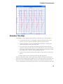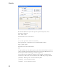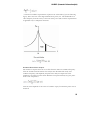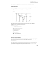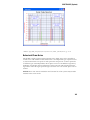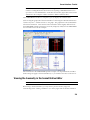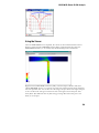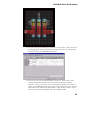
1
Simulation
Copyright Notice
Copyright 1994-2007 Agilent Technologies, Inc. All rights reserved.
Notice
The information contained in this document is subject to change without notice.
Agilent Technologies makes no warranty of any kind with regard to this material,
including, but not limited to, the implied warranties of merchantability and fitness for a
particular purpose. Agilent Technologies shall not be liable for errors contained herein or
for incidental or consequential damages in connection with the furnishing, performance,
or use of this material.
Warranty
A copy of the specific warranty terms that apply to this software product is available upon
request from your Agilent Technologies representative.
U.S. Government Restricted Rights
Software and technical data rights granted to the federal government include only those
rights customarily provided to end user customers. Agilent provides this customary
commercial license in Software and technical data pursuant to FAR 12.211 (Technical
Data) and 12.212 (Computer Software) and, for the Department of Defense, DFARS
252.227-7015 (Technical Data - Commercial Items) and DFARS 227.7202-3 (Rights in
Commercial Computer Software or Computer Software Documentation).
© Agilent Technologies, Inc. 1994-2007
395 Page Mill Road, Palo Alto, CA 94304 U.S.A.
Acknowledgments
Mentor Graphics is a trademark of Mentor Graphics Corporation in the U.S. and other
countries.
Microsoft®, Windows®, MS Windows®, Windows NT®, and MS-DOS® are U.S.
registered trademarks of Microsoft Corporation.
Pentium® is a U.S. registered trademark of Intel Corporation.
PostScript® and Acrobat® are trademarks of Adobe Systems Incorporated.
UNIX® is a registered trademark of the Open Group.
Java(TM) is a U.S. trademark of Sun Microsystems, Inc.
SystemC® is a registered trademark of Open SystemC Initiative, Inc. in the United States
and other countries and is used with permission.
Drawing Interchange file (DXF) is a trademark of Auto Desk, Inc.
EMPOWER/ML, GENESYS, SPECTRASYS, HARBEC, and TESTLINK are
trademarks of Eagleware-Elanix Corporation.
GDSII is a trademark of Calma Company.
Sonnet is a registered trademark of Sonnet Software, Inc.
Table Of Contents
Chapter 1:
Overview ....................................................................................................................1
Simulations...........................................................................................................................................1
Which Simulator Should I Use? .......................................................................................................1
Ports......................................................................................................................................................4
Chapter 2:
Linear Analysis ..........................................................................................................5
Overview..............................................................................................................................................5
Linear Analysis Properties.................................................................................................................6
S Parameters ........................................................................................................................................8
Overview..........................................................................................................................................8
S-Parameter Basics .........................................................................................................................8
Stability.......................................................................................................................................... 10
Matching ....................................................................................................................................... 11
GMAX and MSG ........................................................................................................................ 12
The Unilateral Case ..................................................................................................................... 13
Gain Circles .................................................................................................................................. 13
Noise Circles ................................................................................................................................ 14
Smith Chart................................................................................................................................... 15
Linear Analysis Output................................................................................................................... 16
Chapter 3:
DC Analysis ............................................................................................................. 21
DC Analysis Overview ................................................................................................................... 21
DC Analysis Properties................................................................................................................... 22
DC Analysis Output........................................................................................................................ 25
Chapter 4:
CAYENNE (Transient Analysis) ............................................................................27
CAYENNE Overview.................................................................................................................... 27
CAYENNE Walkthrough.............................................................................................................. 27
Simulation Time Steps .................................................................................................................... 31
Numerical Precision.................................................................................................................... 33
Frequency-dependent Models ....................................................................................................... 34
Convergence Criteria....................................................................................................................... 37
Integrator and Predictor................................................................................................................. 38
Cayenne Options ............................................................................................................................. 39
Chapter 5:
HARBEC (Harmonic Balance Analysis).................................................................45
v
Simulation
HB (Harmonic Balance) Analysis ................................................................................................. 45
Harmonic Balance Overview..................................................................................................... 45
HARBEC Options ...................................................................................................................... 45
HARBEC Popup Menu ............................................................................................................. 53
Solving Convergence Issues....................................................................................................... 53
Optimizing Simulation Performance ....................................................................................... 54
Harmonic Balance Analysis Functions .................................................................................... 57
Table 1. Basic HB analysis Measurements ............................................................................. 62
HB Oscillator Analysis.................................................................................................................... 67
Oscillator Design Overview....................................................................................................... 67
Measurement ................................................................................................................................ 76
Harmonic Balance Oscillator Options..................................................................................... 77
Harbec Nonlinear Noise ................................................................................................................ 79
Nonlinear Noise Overview........................................................................................................ 79
Performing a Nonlinear Noise Simulation.............................................................................. 79
Basic Concepts............................................................................................................................. 84
Oscillator Noise Simulation....................................................................................................... 84
Mixer Noise Simulation.............................................................................................................. 94
Entering Nonlinear Models ........................................................................................................... 98
Chapter 6:
Advanced Modeling Kit .......................................................................................... 99
Advanced Modeling Kit Overview............................................................................................... 99
Using the Additional AMK Models ............................................................................................. 99
Creating New Verilog-A Models................................................................................................. 100
Customizing Built-In Nonlinear Models ................................................................................... 101
Verilog-A Tutorial ......................................................................................................................... 101
Verilog-A Reference...................................................................................................................... 103
Verilog-A Reference Overview ............................................................................................... 103
Preprocessor............................................................................................................................... 103
Data Types and Parameters ..................................................................................................... 104
Analog Block.............................................................................................................................. 107
Analog Functions ...................................................................................................................... 112
System tasks and functions ...................................................................................................... 113
Eagleware Verilog-A Extensions ............................................................................................ 114
Chapter 7:
SPECTRASYS (System)......................................................................................... 119
Spectral Propagation and Root Cause Analysis (SPARCA) ................................................... 119
Getting Started ............................................................................................................................... 120
SPECTRASYS Walkthrough Overview ................................................................................ 120
Create a System Schematic....................................................................................................... 120
Add a System Analysis.............................................................................................................. 122
vi
Table Of Contents
Run the Simulation.................................................................................................................... 124
Add a Graph or Table .............................................................................................................. 125
Fundamentals ................................................................................................................................. 127
General Behavioral Model Overview..................................................................................... 127
Sources ........................................................................................................................................ 128
Channels...................................................................................................................................... 129
Specifying Paths......................................................................................................................... 130
Level Diagrams .......................................................................................................................... 131
Spectrum Plots and Tables ...................................................................................................... 134
Identifying Spectral Origin....................................................................................................... 136
Broadband Noise....................................................................................................................... 138
Propagation Basics .................................................................................................................... 140
Controlling Analysis Data ........................................................................................................ 141
Advanced ........................................................................................................................................ 142
Non Linear Model Behavior.................................................................................................... 142
Cascaded Noise Analysis.......................................................................................................... 142
Cascaded Noise Figure Equations.......................................................................................... 145
Coherency................................................................................................................................... 146
Intermod and Harmonic Basics .............................................................................................. 149
Intermod Path Measurement Basics ...................................................................................... 153
Cascaded Intermod Equations................................................................................................ 155
In-Band Intermod Path Measurements................................................................................. 156
Out-of-Band Intermod Path Measurements......................................................................... 157
Troubleshooting Intermod Path Measurements.................................................................. 158
Single Sideband to AM and PM Decomposition................................................................. 159
Behavioral Phase Noise............................................................................................................ 161
Spectrum Analyzer Display...................................................................................................... 164
Synthesis...................................................................................................................................... 167
Directional Energy (Node Voltage and Power) ................................................................... 169
Transmitted Energy .................................................................................................................. 170
Increasing Simulation Speed.................................................................................................... 170
Reducing the File Size............................................................................................................... 172
Measurements ................................................................................................................................ 173
SPECTRASYS Measurement Index ...................................................................................... 173
General........................................................................................................................................ 179
Power........................................................................................................................................... 183
Voltage ........................................................................................................................................ 204
Troubleshooting ............................................................................................................................ 207
General RF Architecture Troubleshooting........................................................................... 207
How come my noise figure decreases through a cascade? ................................................. 209
Why don't I get the same answer as my spreadsheets? ....................................................... 209
No Attenuation Across a Filter............................................................................................... 210
vii
Simulation
Dialog Box Reference ................................................................................................................... 212
System Simulation Parameters - General Tab ...................................................................... 212
System Simulation Parameters - Paths Tab........................................................................... 213
Add / Edit Path Dialog Box ................................................................................................... 215
System Simulation Parameters - Calculate Tab .................................................................... 219
System Simulation Parameters - Composite Spectrum Tab............................................... 221
System Simulation Parameters - Options Tab...................................................................... 225
System Simulation Parameters - Output Tab ....................................................................... 227
Chapter 8:
Parameter Sweeps ..................................................................................................229
Parameter Sweep............................................................................................................................ 229
Performing a Parameter Sweep ...................................................................................................229
Parameter Sweep Properties ........................................................................................................ 232
Chapter 9:
Device Data............................................................................................................235
Linear vs. Nonlinear Device Models.......................................................................................... 235
Linear Data Overview................................................................................................................... 235
Using a Data File in GENESYS ................................................................................................. 235
Provided Device Data................................................................................................................... 236
Creating New Linear Data Files.................................................................................................. 236
File Record Keeping...................................................................................................................... 238
Exporting Data Files..................................................................................................................... 238
Noise Data in Data Files .............................................................................................................. 238
Chapter 10:
Measurements: Overview....................................................................................... 241
Overview......................................................................................................................................... 241
Linear Measurements .................................................................................................................... 241
Nonlinear Measurements ............................................................................................................. 243
Operators ........................................................................................................................................ 243
Sample Measurements .................................................................................................................. 244
Using Non-Default Simulation/Data......................................................................................... 245
Using Equation Results (post-processing) ................................................................................ 245
Chapter 11:
Measurements: Linear............................................................................................247
S-Parameters................................................................................................................................... 247
H-Parameters.................................................................................................................................. 248
Y-Parameters .................................................................................................................................. 249
Z-Parameters .................................................................................................................................. 249
Voltage Standing Wave Ratio (VSWR) ...................................................................................... 250
Input Impedance / Admittance (ZINi, YINi).......................................................................... 251
Voltage Gain................................................................................................................................... 251
viii
Table Of Contents
Noise Measure (NMEAS)............................................................................................................ 252
Noise Figure (NF) / Minimum Noise Figure (NFMIN)........................................................ 252
Constant Noise Circles (NCI) ..................................................................................................... 253
Noise Correlation Matrix Parameters ........................................................................................ 254
Simultaneous Match Gamma at Port i (GMi)........................................................................... 254
Simultaneous Match Admittance / Impedance at Port i (ZMi, YMi) ................................. 254
Maximum Available Gain (GMAX)........................................................................................... 255
Available Gain & Power Gain Circles (GA, GP)..................................................................... 255
Unilateral Gain Circles at Port i (GU1, GU2) .......................................................................... 256
Stability Factor (K), Stability Measure (B1)............................................................................... 257
Input / Output Plane Stability Circles (SB1, SB2)................................................................... 257
Optimal Gamma for Noise (GOPT) ......................................................................................... 258
Optimal Admittance / Impedance for Noise (YOPT, ZOPT)............................................. 259
Effective Noise Input Temperature (NFT) .............................................................................. 259
Normalized Noise Resistance (RN) ........................................................................................... 260
Reference Impedance (ZPORTi)................................................................................................ 260
Chapter 12:
Measurements: Nonlinear ..................................................................................... 263
Port Power (PPORT).................................................................................................................... 263
Port Voltage (VPORT)................................................................................................................. 263
Node Voltage (Vnode) ................................................................................................................. 264
Reference Impedance (ZPORT)................................................................................................. 264
Large Signal S-Parameters............................................................................................................ 265
Intercept Point Calculation.......................................................................................................... 268
Chapter 13:
Measurements: Load Pull ...................................................................................... 271
Load Pull Contours ....................................................................................................................... 271
To create contours from a load pull data file:....................................................................... 272
Chapter 14:
Sonnet Interface: Tutorial...................................................................................... 273
Introduction.................................................................................................................................... 273
Creating a Layout Without a Schematic..................................................................................... 273
Simulating the Layout ................................................................................................................... 273
Viewing Results.............................................................................................................................. 275
Using the Current and Far Field Viewers.................................................................................. 276
Creating a Layout From an Existing Schematic ....................................................................... 276
Simulating the Layout with Lumped Elements ........................................................................ 278
Viewing the Geometry in the Sonnet Native Editor............................................................... 279
Chapter 15:
Sonnet Interface: Design Flow .............................................................................. 281
Sonnet Flow Overview................................................................................................................. 281
ix
Simulation
Deleting Internal Simulation Data.............................................................................................. 281
Manual Mode.................................................................................................................................. 282
Chapter 16:
Sonnet Interface: Translation Details ....................................................................285
Sonnet Options Dialog Box ........................................................................................................ 285
General Tab................................................................................................................................ 285
Sonnet features supported in GENESYS ................................................................................. 287
Sonnet features not supported in GENESYS Interface......................................................... 288
Category 1 – Sonnet features directly affecting frequencies, geometry and subsectioning288
Category 2 – Features available in GENESYS other ways ................................................ 289
Category 3 – Cosmetic Sonnet features which do not directly affect simulation........... 289
EMPOWER features not supported by the Sonnet Interface............................................... 289
Chapter 17:
EMPOWER: Planar 3D EM Analysis.................................................................... 291
EMPOWER: Basics ...................................................................................................................... 291
Overview..................................................................................................................................... 291
Basic Geometry.......................................................................................................................... 291
The Grid...................................................................................................................................... 295
Viaholes and Z-Directed Ports ............................................................................................... 298
EM Ports..................................................................................................................................... 299
EMPOWER Options ............................................................................................................... 299
General Tab................................................................................................................................ 300
Viewer / Far Field Tab............................................................................................................. 301
Advanced Tab ............................................................................................................................ 303
Simulation Status Window.......................................................................................................304
Batch Runs.................................................................................................................................. 305
EMPOWER: Operation............................................................................................................... 305
Overview..................................................................................................................................... 305
Features ....................................................................................................................................... 305
Examples..................................................................................................................................... 306
Creating a Layout Without a Schematic................................................................................. 307
Creating a Layout....................................................................................................................... 308
Box Dimensions ........................................................................................................................ 308
General Layers ........................................................................................................................... 309
EMPOWER Layers................................................................................................................... 310
Drawing the Layout................................................................................................................... 312
Centering the Layout................................................................................................................. 314
Placing EMPOWER Ports....................................................................................................... 314
Simulating the Layout ............................................................................................................... 315
Viewing Results.......................................................................................................................... 317
Using the Viewer ....................................................................................................................... 319
x
Table Of Contents
Creating a Layout From an Existing Schematic................................................................... 320
Simulating the Layout ............................................................................................................... 321
Lumped Elements ..................................................................................................................... 323
Real-Time Tuning...................................................................................................................... 323
EMPOWER: Tips ......................................................................................................................... 324
Overview..................................................................................................................................... 324
Cell Size....................................................................................................................................... 325
Maximum Critical Frequency .................................................................................................. 325
Symmetry .................................................................................................................................... 326
Thinning Out ............................................................................................................................. 327
Wall & Cover Spacing............................................................................................................... 327
Cover Type ................................................................................................................................. 327
Lossy Analysis ............................................................................................................................ 328
Viewer Data................................................................................................................................ 328
Slot-Type Structure ................................................................................................................... 328
Preferred Cell Count................................................................................................................. 329
Thick Metal................................................................................................................................. 330
EMPOWER: External Ports ....................................................................................................... 331
Overview..................................................................................................................................... 331
Placing External Ports .............................................................................................................. 331
EMPort Options........................................................................................................................ 332
Deembedding............................................................................................................................. 334
MultiMode Ports........................................................................................................................ 335
Generalized S-Parameters ........................................................................................................ 337
EMPOWER: Decomposition ..................................................................................................... 338
Overview..................................................................................................................................... 338
Basics ........................................................................................................................................... 339
Spiral Inductor Example .......................................................................................................... 340
Losses .......................................................................................................................................... 345
Port Numbering......................................................................................................................... 346
EMPOWER: Lumped Elements and Internal Ports............................................................... 347
Overview..................................................................................................................................... 347
Placing Internal Ports ............................................................................................................... 347
Manually Adding Lumped Elements...................................................................................... 348
Automatic Port Placement....................................................................................................... 349
Planar (X- and Y-Directed) Ports........................................................................................... 350
Resonance................................................................................................................................... 351
EMPOWER: Box Modes............................................................................................................. 351
Overview..................................................................................................................................... 351
Homogeneous Rectangular Cavity ......................................................................................... 352
Higher Order Box Modes ........................................................................................................ 353
Partial Dielectric Loading......................................................................................................... 353
xi
Simulation
Signal Metal Effects................................................................................................................... 354
Top Cover................................................................................................................................... 354
Cavity Absorber......................................................................................................................... 354
EMPOWER: Viewer and Antenna Patterns............................................................................. 355
Overview..................................................................................................................................... 355
Interface ...................................................................................................................................... 355
Far-Field Radiation Pattern Viewer........................................................................................ 360
Examples..................................................................................................................................... 363
MultiMode Viewer Data........................................................................................................... 367
Via Hole Viewer Example ....................................................................................................... 368
Viewer Theory............................................................................................................................ 369
Summary ..................................................................................................................................... 371
EMPOWER: File Descriptions................................................................................................... 371
Overview..................................................................................................................................... 371
Text Files vs. Binary Files......................................................................................................... 372
File Extensions........................................................................................................................... 372
.EMV (EMPOWER Viewer) Files ......................................................................................... 373
.L1, .L2, ... .Ln (Line Data) Files ............................................................................................. 373
.LST (Listing) Files .................................................................................................................... 374
.PLX (Current/Viewer Data) Files......................................................................................... 375
.R1, .R2, ... Rn (Port Impedance) Files .................................................................................. 375
.RGF (Line Data) Files ............................................................................................................. 376
.RX (Frequency vs. Impedance) Files .................................................................................... 376
.SS (S Parameter) Files .............................................................................................................. 376
.TPL (Topology) Files............................................................................................................... 377
.WSX (Workspace) Files........................................................................................................... 377
.Y (Y-Parameter) Files .............................................................................................................. 377
~SS, ~RG, etc. (Backup) Files ................................................................................................ 377
EMPOWER: Advanced M/FILTER Example ....................................................................... 377
EMPOWER Advanced Example: Filter Synthesis.............................................................. 377
EMPOWER: Theory .................................................................................................................... 392
Overview..................................................................................................................................... 392
Historical Background .............................................................................................................. 393
Problem Formulation................................................................................................................ 393
Method of Lines ........................................................................................................................ 395
Mapping on the Grid ................................................................................................................ 396
Grid Green's Function.............................................................................................................. 398
Informational Multiport ........................................................................................................... 399
Numerical Acceleration Procedures....................................................................................... 400
De-Embedding Algorithm....................................................................................................... 402
EMPOWER: References.............................................................................................................. 402
General Background ................................................................................................................. 402
xii
Table Of Contents
The Method of Lines ................................................................................................................ 404
Richardson's Extrapolation...................................................................................................... 404
Symmetry Processing................................................................................................................ 405
EMPOWER Engine Theory and Algorithms ...................................................................... 405
Test Examples and Comparisons ........................................................................................... 406
Index
407
xiii
Chapter 1:
Overview
Simulations
GENESYS supports several different types of analysis, allowing the exploration of a
complete range of circuit performance. A simulation run is when you run an analysis on a
circuit.
•
DC Simulation (nonlinear) (a part of HARBEC)
•
Linear S-Parameter Simulation
•
Planar 3D Electromagnetic (EM) Simulation (EMPOWER)
•
Harmonic Balance Simulation (nonlinear) (HARBEC)
•
Spectral Domain System Simulation (SPECTRASYS)
•
Transient Simulation (nonlinear, time domain) (CAYENNE)
Additionally, the following items are available:
•
Parameter Sweep
•
TESTLINK (Covered in the User's Guide).
Several of these capabilities work together. EM co-simulates directly with the linear and
DC circuit simulators and indirectly with HARBEC, SPECTRASYS, and CAYENNE;
combining the accuracy of EM analysis with the generality and speed of circuit
simulation. Parameters sweeps can be used with any analysis type as well as with other
sweeps. Frequency, resistance, substrate height, and DC supply level are just a few of the
parameters that are typically swept.
To create a new Analysis:
1. Click the New Item button (
Analysis.
) on the Workspace Tree toolbar and select
2.
Select which Analysis you want to add.
3.
Define the analysis properties and click OK or Calculate Now to run the simulation.
Which Simulator Should I Use?
Often, we at Eagleware are asked which simulation method should be used in a particular
circuit: Linear Analysis? Nonlinear (HARBEC)? SPICE (by exporting)? Electromagnetic
(EMPOWER)? SPECTRASYS?
1
Simulation
For most circuits, you will use a combination of the different simulations. We have
developed several guidelines that should simplify the decision for most applications. First,
each method has benefits and drawbacks:
Benefits
Linear
CAYENNE
EMPOWER
HARBEC
Extremely fast
Time domain
Extremely accurate
Steady-State Nonlinear
Schematic or netlist
Schematic or netlist
Does not require an
intimate knowledge of the
circuit – simulator figures
out coupling, etc.
Study mixing,
compression and
intermodulation
Real-time tuning of
circuits
Starting waveforms
(e.g. oscillator startup)
Can predict radiation,
current distribution.
DC biasing
information
Uses manufacturerprovided measured
data
DC biasing information Automatic deembedding
Lots of vendorsupplied models
Requires very little
memory
Predicts box mode effects
Lots of vendor-supplied
(e.g. What happens if the
models
circuit is placed in a box?)
Use frequency
dependent equations
and post-processing
Easily use equations
and user functions
Non-linear modeling of Can use arbitrary shapes –
Use measured data in
crossover distortion,
does not require an existing
simulation
etc.
model for them
No time domain
Very slow for near
harmonic data
No biasing
information
Very hard to model
frequency domain
Requires lots of memory
behavior (e.g. unloaded
Q)
Takes a lot of memory
and time
Everything is linear
Does not model noise
performance
Discretizes metal patterns
to fit grid
Requires nonlinear
models
Requires knowledge
Requires knowledge of
of circuit – coupling
circuit – coupling
factors, parasitics, etc. factors, parasitics, etc.
Can be difficult to set up a
circuit for simulation
Cannot study transient
behavior (for example,
oscillator startup)
Drawbacks
Extremely slow
Much slower than
linear
In determining which simulation type to use, several points should be considered:
Linear or Electromagnetic?
1.
2
Should I use both circuit theory and EM simulation? Circuit theory
simulation in GENESYS is amazingly fast and interactive. No other program at
any price approaches the speed of GENESYS. EMPOWER simulations are
more accurate and do not require the use of specific geometric objects for which
circuit models have been developed. EM simulation complements rather than
replaces circuit theory simulation.
Overview
2.
What is the highest frequency used in the circuit? If below about 1 GHz,
lumped elements are often used in place of distributed elements. In this case, the
final board layout usually won’t add any significant parasitics or coupling
concerns. Often, however, customers use EMPOWER to simulate the final
board layout to make sure that it doesn’t differ from the linear simulation.
3.
How big is the circuit? If the circuit itself is very small compared to a
wavelength at the highest frequency of concern, electromagnetic simulation may
not be needed. This is because resonances occur at quarter wavelengths, and
circuits much smaller than this usually behave as predicted by a complete linear
simulation.
4.
Does the circuit have non-standard metal shapes, patterns, or geometries?
If so, electromagnetic simulation may be the only option. EMPOWER can
simulate any arbitrary shape, such as ground plane pours. A linear simulator
requires a netlist or schematic to describe the circuit, so models would have to
exist for the pattern that you plan to simulate.
5.
Do any of the models in the circuit exceed or come close to exceeding the
published parameter ranges? If so, you may want to verify the simulation with
EMPOWER, or use EMPOWER exclusively. Most of the models in GENESYS
were derived from measured data, which was only taken for particular parameter
variations.
Linear or Harmonic Balance?
This question is the easiest to answer: for active circuits you will usually use both. For
passive circuits (filters, couplers, power dividers, etc), you will only use linear. Passive
circuits are linear-harmonic balance will not give you extra information that you could not
get from linear simulation. Active circuits are inherently nonlinear. Harmonic balance will
help you analyze DC operating points and nonlinear performance.
For both active and passive circuits, linear simulation is the workhorse of RF design.
Matching, noise, and stability studies are all completed quickly using linear simulation.
Harmonic balance is used to complete the analysis of most circuits. Examine mixer
conversion gain, amplifier compression, and detector efficiency using harmonic balance.
Linear or CAYENNE (Transient)?
Often, this question does not have a quick answer. For example, many engineers associate
CAYENNE with time domain simulation, and a linear simulator with frequency domain
simulation. Actually, many circuits have data of interest in both the time and frequency
domains, which could warrant the use of both simulators. For example, an oscillator has
phase noise, transmission, and phase characteristics, which are all frequency domain
measurements. Oscillators also have waveform magnitude, starting time, and startup
transients, which are all time domain measurements. In this case, both simulators can be
used in the circuit design.
There are some guidelines for deciding between CAYENNE and linear simulation:
1.
Does the circuit depend on time domain characteristics? If so, CAYENNE
must be used for this portion of the design. If the circuit depends entirely on the
3
Simulation
time domain, CAYENNE can be used exclusively. However, if a frequency
domain response is also of interest, linear simulation may be used in addition to
CAYENNE .
Often, both CAYENNE and linear simulation are useful in a design. For example, in
amplifier design, the linear portion (gain, matching) can be done in the linear simulator,
and the device biasing can be done in CAYENNE .
Ports
Using Ports in the Design
Note: The information in this section does not apply to EMPOWER simulation.
In GENESYS, ports serve two different purposes:
1) In a top level design specified for simulation, ports used directly for simulation.
The impedances of the ports define the impedances used in the simulator. Inputs
with sources (such as INP_PAC [input port with power source] and INP_VDC
[input port with DC voltage]) are in full effect when placed on the top level.
2) In lower level designs, single terminal ports are only used to provide connection
information for subcircuits. Impedances and sources (such as INP_PAC and
INP_VAC) are ignored. To place sources in subcircuits, you must use sources
without ports (such as PAC and VAC). Note: Balanced (two-terminal) ports are
retained from all levels in the design, essentially becoming top-level ports.
With this configuration, you can test a subcircuit in linear and nonlinear modes by putting
the sources for test within the ports. When the subcircuit is then reused inside the larger
circuits, those circuits and ports will be disabled. If you actually want to create a true port
within a subcircuit, you can place a balanced port inside the subnetwork. If you only want
a single-ended port, simply ground the negative terminal of the differential port.
New in GENESYS 2005: You can use equation variables to specify port numbers, plus
you can create user models which contain ports. For an examples, load the system
intermod source into a workspace: Use “Add From library” in the create new item button
in the workspace tree. Select the system intermod source, then look at the design and
equations.
New in GENESYS 2005: Balanced (differential) ports are supported in all simulators.
To place a differential port, go to the part selected and search the Eagleware part library
for “Balanced”.
If ports are used on the master design, they must be placed in sequential order. Top-level
ports are required for linear simulation and are strongly recommended for SPECTRASYS.
Ports are optional for DC simulation, HARBEC, and CAYENNE. Other than the
symbols, there is no difference between standard input and output ports. To use a
complex port impedance, you can either directly use a complex number in the port
termination or you can use a 1-port data file.
4
Chapter 2:
Linear Analysis
Overview
Linear simulation calculates S-parameters and noise parameters of a schematic design. If
the circuit contains nonlinear elements, DC simulation is first run automatically and the
nonlinear devices are linearized at the DC operating point.
Port Impedance Usage
• The design must have input/output ports in sequential order.
• Balanced Ports are fully supported.
• All impedances are specified on the design’s ports.
• To use a complex port impedance, you can either directly use a complex number
in the port termination or you can use a 1-port data file.
To add a linear analysis:
1.
Create a design with a schematic.
2.
Click the New Item button (
) on the Workspace Tree toolbar and
choose "Add Linear Analysis" from the Analyses menu.
3.
Define the Analysis Properties and click OK.
4.
The analysis runs and creates a data set.
Note: S-Parameters are calculated with respect to ports; you must have ports in the
schematic numbered in ascending order from 1 to run a linear analysis.
See also:
Measurements (later in this manual)
Outputs Overview, User's Guide
5
Simulation
Linear Analysis Properties
6
Name
Description
Name
Name of Analysis
Design
Design on which the Linear Analysis is run
Dataset
Dataset file in which the data is saved. If not specified,
the dataset name will be the name of the analysis with
"_Data" appended.
Description
Description of the analysis being run. For
documentation purposes only, not otherwise used by
GENESYS.
DC Analysis
If you select (default) it will use an internal DC Analysis
(with default options) to set operating point. Or, you can
select a DC Analysis to have operating point calculated
using a custom DC set of options.
Calculate Now
Runs the analysis, regardless of whether or not any
changes were made.
Linear Analysis
Factory Defaults
Reset all values to their default
Save As Favorite
Close the dialog and establish the analysis settings as a
default for the "new" operation. When you create a new
linear analysis it will look just like this favorite.
Calculate Noise
Enable this to have the linear analysis create a CS noise
correlation matrix. If this is disabled, NF can not be
calculated. Disable this to increase calculation speed and
reduce storage requirements.
GMin
GMin is an admittance added into the circuit if the
circuit is not invertible (for example a capacitor of
infinite Q to ground). Change this only to increase
dynamic range of the analysis if your circuit values are
clumped higher.
Preferred
Reduction
Size
When Linear Analysis creates a matrix tree this is the
optimal size of the branches. Increasing this may reduce
execution time. Decreasing this will tend to increase
tuning speed at the expense of overall execution speed.
Start
Frequency
The lower bound (minimum frequency) of the linear
simulation. Equations may be used here (no = needed).
Stop
Frequency
The upper bound (maximum frequency) of the linear
simulation. Equations may be used here (no = needed).
Frequency
Units
Unit of measure used to specify the frequency.
Temperature
Ambient temperature at which the linear analysis is
performed, specified in the unit of measure chosen from
the drop-down menu.Equations may be used here (no =
needed).
Linear:
Number of
Points
Number of points in entire simulation. Equations may
be used here (no = needed).
Advanced
Frequency
Range
Type of
Sweep
Log:
Number of points in every decade. Equations may be
Points/Decade used here (no = needed).
7
Simulation
Linear: Step
Size (MHz)
Allows specification of start and stop frequencies, and
space between points. Equations may be used here (no
= needed).
List of
Frequencies
(MHz)
Allows the explicit specification of analysis frequencies.
These points are entered into the List of Frequencies
box separated by spaces. Equations may be used here
(no = needed).
S Parameters
Overview
The purpose of this section is to summarize network analysis concepts and to define some
of the parameters plotted by GENESYS. For further details on measurements, see the
Measurements section of this manual.
Networks are considered as "black boxes". Because the networks are assumed to be linear
and time invariant, the characteristics of the networks are uniquely defined by a set of
linear equations relating port voltages and currents. A number of network parameter types
have been developed for this purpose, including H, Y, Z, S, ABCD, and others. These
parameters may be used to compute and display network responses and to compute
quantities useful for circuit design such as Gmax (maximum gain) and gain circles. Each
parameter type has advantages and disadvantages. Carson [1] and Altman [2] provide
additional information.
S-Parameter Basics
S-parameters have earned a prominent position in RF circuit design, analysis, and
measurement. Parameters used earlier in RF design, such as Y-parameters, require opens
or shorts on ports during measurement. This is a nearly impossible constraint for highfrequency broadband measurements. Scattering parameters [3, 4] (S-parameters) are
defined and measured with the ports terminated in a characteristic reference impedance.
Modern network analyzers are well suited for measuring S-parameters. Because the
networks being analyzed are often employed by insertion in a transmission medium with a
common characteristic reference impedance, S-parameters have the additional advantage
that they relate directly to commonly specified performance parameters such as insertion
gain and return loss.
Two-port S-parameters are defined by considering a set of voltage traveling waves. When
a voltage wave from a source is incident on a network, a portion of the voltage wave is
8
Linear Analysis
transmitted through the network, and a portion is reflected back toward the source.
Incident and reflected voltage waves may also be present at the output of the network.
New variables are defined by dividing the voltage waves by the square root of the
reference impedance. The square of the magnitude of these new variables may be viewed
as traveling power waves.
|a1|2 = incident power wave at the network input
|b1|2 = reflected power wave at the network input
|a2|2 = incident power wave at the network output
|b2|2 = reflected power wave at the network output
These new variables and the network S-parameters are related by the expressions:
b1 = a1S11 + a2S12
b2 = a1S21 + a2S22
S11 = b1/a1, a2 = 0
S12 = b1/a2, a1 = 0
S21 = b2/a1, a2 = 0
S22 = b2/a2, a1 = 0
Terminating the network with a load equal to the reference impedance forces a2 = 0.
Under these conditions
S11 = b1/a1
S21 = b2/a1
S11 is then the network input reflection coefficient and S21 is the gain or loss of the
network.
Terminating the network at the input with a load equal to the reference impedance and
driving the network from the output port forces a1 = 0. Under these conditions
S22 = b2/a2
S12 = b1/a2
S22 is then the network output reflection coefficient and S12 is the reverse gain or loss of
the network.
Linear S-parameters are unitless. Since they are based on voltage waves, they are converted
to decibel format by multiplying the log of the linear ratio by 20. It is not always obvious
whether an author is referring to linear or decibel parameters. To avoid this confusion, the
book Oscillator Design and Computer Simulation and Versions 5.4 and earlier of
SUPERSTAR use C for linear S-parameters and S for the decibel form. This is somewhat
unconventional. Version 6.0 and later of GENESYS also supports the convention
MAG[S21] which is linear and DB[S21] which is the decibel form. With reflection
parameters, the linear form is often referred to as a reflection coefficient and the decibel
form as return loss.
S11(dB)=input reflection gain=20 log S11
9
Simulation
S22 (dB)=output reflection gain=20 log S22
S21(dB)=forward gain=20log S21
S12(dB)=reverse gain=20log S12
S21 and S12 are the forward and return gain (or loss) when the network is terminated with
the reference impedance. The gain when matching networks are inserted at the input,
output, or both is described later.
S11 and S22 coefficients are less than 1 for passive networks with positive resistance.
Therefore, the input and output reflection gains, S11 and S22, are negative decibel numbers.
Throughout Eagleware material, the decibel forms S11 and S22 are referred to as return
losses, in agreement with standard industry convention. To be mathematically correct,
they have been left as negative numbers. As such, the rigorous convention would be to
call them return gain.
Input VSWR (VSWR1) and S11 are related by
VSWR1 = ( 1 + |S11| ) / ( 1 - |S11| )
The output VSWR is related to S22 by an analogous equation. A circle of constant radius
centered on the Smith chart is a circle of constant VSWR. The complex input impedance
is related to the input reflection coefficients by the expression:
I1 = Zo ( 1 + S11 ) / ( 1 - S11 )
The output impedance is similarly related to S22.
Stability
Because S12 of devices is not zero, a signal path exists from the output to the input. This
feedback path creates an opportunity for oscillation. The stability factor, K, is
K = ( 1 - |S11|2 - |S22|2 + |D|2 ) / (2 |S12| |S21|)
where
D = S11S22 - S12S21
From a practical standpoint when K>1, S11<1, and S22<1, the two-port is unconditionally
stable. These are often stated as sufficient to insure stability. Theoretically, K>1 is
insufficient to insure stability, and an additional condition should be satisfied. One such
parameter is B1 which should be greater than zero.
B1 = 1 + |S11|2 - |S22|2 - |D|2 > 0
Stability circles may be used for a more detailed analysis. The load impedances of a
network which ensure that S11<1 are identified by a circle of radius R centered at C on a
Smith chart. The output plane stability circle is
Cout = (S22 - DS11*)* / (|S22|2 - |D|2), Rout = | S12S21 / (|S22|2 - |D|2) |
This circle is the locus of loads for which S11 = 1. The region inside or outside the circle
may be the stable region.
10
Linear Analysis
The input plane stability circle equations are the same as the output plane equations, with
1 and 2 in the subscripts interchanged.
Shown in the figure below are the input plane stability circles on the left and the output
plane stability circles on the right for the Avantek AT10135 GaAsFET. The shaded
regions are potentially unstable. At the input, the stability circle with marker 1 indicates
sources with a small resistive component and inductive reactance of about 200 ohms are
unstable. Circles 2 and 3 are also unstable with low resistance and certain inductive source
impedances. At the output plane on the right, at 500 MHz, a wide range of inductive loads
is potentially unstable.
When designing an amplifier the first step is to examine the stability circles of the device
without the matching circuit present. The grounding which will be present at the emitter
or source should be included in the analysis. This stability data is used to 1) add stabilizing
components such as shunt input and output resistors for bipolars or inductance in the
source path for GaAsFETs and to 2) select an input and output matching network
topology which properly terminates the device (at low and high frequencies) for stability.
In the example above, matching networks with a small series capacitor adjacent to the
device would insure capacitive loads at low frequencies, thus enhancing stability. This is
probably sufficient for the input. However, considering that device S-parameter data is
approximate and since the output plane of this device is more threatening, it would be
prudent to stabilize this device in addition to using series capacitors.
Note: Stability should be checked not only at the amplifier operating frequencies, but
also over the entire frequency range for which S-Parameter data is available.
Matching
One definition of network gain is the transducer power gain, Gt: Transducer power gain is
the power delivered to the load divided by the power available from the source.
Gt = P(delivered-to-load) / P(available-from-source)
Other gain definitions include the power gain, Gp, and the available power gain, Ga.
Gp = P(delivered-to-load) / P(input-to-network)
11
Simulation
Ga = P(available-from-network) / P(available-from-source)
The S-parameter data for the network is measured with a source and load equal to the
reference impedance. If the network is not terminated in the reference impedance, Gt can
be computed from the reflection coefficients of the terminations on the network and the
S-parameters of the network. At this point we have multiple sets of reflection coefficients:
those of the terminations and S11 and S22 of the network. To avoid confusion the
termination reflection coefficients are given a different symbol, G.
The transducer power gain with the network inserted in a system with arbitrary source and
load reflection coefficients is [4]:
Gt = ( |S21|2 (1 - |Rs|2)(1 - |RL|2) ) / |(1 - S11RS)(1 - S22RL) - S21S12RLRS|2
where
RS = reflection coefficient of the source
RL = reflection coefficient of the load
If and are both zero, then
Gt=S21
or
Gt(dB)=20log S21=S21(dB)
Therefore, when a network is installed in a system with source and loads equal to the
reference impedance, S21 is the network transducer power gain in decibels.
Because S11 and S22 of a network are not in general zero, a portion of the available source
power is reflected from the network input and is dissipated in the source. The insertion of
a lossless matching network at the input (and/or output) of the network could increase
the gain of the overall system if reflections toward the source were reduced. Shown below
is a two-port network with lossless matching networks inserted between the network and
the source and load.
GMAX and MSG
When the input and output networks are simultaneously designed for maximum gain,
there is no reflection at the source or load. The maximum transducer power gain, Gmax, is
given by
Gmax = ( |S21| / |S12| ) * (K - sqrt(K2 - 1))
The maximum stable gain, MSG, is defined as Gmax with K=1. Therefore
MSG = |S21| / |S12|
A GENESYS plot of GMAX shows Gmax when K>1 and MSG when K<1.
Again, achieving this maximum gain requires that the input network is designed such that
RS is the complex conjugate of S11 and RL is the complex conjugate of S22. GENESYS
returns the required reflection coefficients, impedance and admittance for the input and
output networks as GM1, GM2, ZM1, ZM2, YM1 and YM2, respectively.
12
Linear Analysis
The Unilateral Case
Historically, to simplify the complex equation for Gt in the previous section on matching,
S12 was set to zero. At higher frequencies, where the device S12 is typically larger, this
assumption is less valid. The assumption simplifies manual and graphical design but is
unnecessary in modern computer-assisted design. The assumption also allows factoring
the above equation into terms that provide insight into the design process. If S12 =0, then
Gtu = ( |S21|2 (1 - |Rs|2)(1 - |RL|2) ) / |(1 - S11RS)(1 - S22RL)|2
where
Gtu=unilateral transducer power gain
When both ports of the network are conjugately matched, and S12 = 0,
Gtu = |S21|2 / ( (1 - |S11|2)(1 - |S22|2) )
The first and third terms indicate the gain increase achievable by matching the input and
output, respectively. If S11 or S22 approach 1, substantial gain improvement is achieved by
matching. Matching not only increases the network gain, but reduces reflections from the
network.
When network gain flatness across a frequency band is more desirable than minimum
reflections, the lossless matching networks are designed to provide a better match at
frequencies where the two-port gain is lower. By careful design of amplifier matching
networks, it is possible to achieve a gain response flat within fractions of a decibel over a
bandwidth of an octave or more.
Gain Circles
When the device is complex conjugately matched, the transducer gain is Gmax and if the
device is terminated with the same resistance used to measure the device S-parameters the
transducer gain is S21. The gain with arbitrary terminations can be visualized on the Smith
chart using gain circles.
GENESYS plots three forms of gain circles: transducer gain unilateral circles, GU1 for
the input network and GU2 for the output network, power gain output network circles,
GP, and available gain input network circles, GA.
Shown below are the input and output unilateral transducer gain circles, GU1 and GU2,
of the Avantek AT10135 GaAsFET transistor. The measurement circles are plotted at the
frequency of the first marker, in this case 2500 MHz. Marker 1 is plotted at the center of
the smallest circle, the point of maximum gain. The gain at the circumference of each
circle of increasing radius is 1 dB lower than the previous inside circle.
13
Simulation
The arc which is orthogonal to the gain circles is the locus of smallest circle center points
from the lowest to highest sweep frequency. Tuning the first marker frequency moves the
center of the circles along this arc.
Notice that a complex conjugate match at the input improves the gain by over 3 dB in
relation to an unmatched 50 ohm source impedance. However, matching the output
provides less than 1 dB gain improvement. An examination of the device S-parameter data
at 2500 MHz reveals that the output is originally closer matched to 50 ohms and it is not
surprising that a matching network would be less beneficial.
Noise Circles
To achieve the best available noise figure from a device the correct impedance must be
presented to the device. The impedance resulting in the best noise performance is in
general neither equal to 50 ohms or the impedance which results in minimum reflection at
the source.
The Avantek AT10135 GaAsFET transistor S-parameter data given earlier includes noise
data. This data is comprised of four numbers for each frequency. These numbers are
NFopt(dB), the optimum noise figure when correctly terminated, Gopt magnitude and
angle, the terminating impedance at the device input which achieves NFopt and Rn/Zo, a
sensitivity factor which effects the radius of the noise circles.
Noise circles plotted by GENESYS for the AT10135 at 2500 MHz are given below.
Circles of increasing radius represent noise figure degradations of 0.25, 0.5, 1, 1.5, 2, 2.5, 3
and 6 dB. In this case, direct termination of the device with a 50 ohm source results in a
degradation of the noise figure of 1 dB. The arc orthogonal to the circles is the locus of
Gopt versus frequency.
14
Linear Analysis
Smith Chart
In 1939, Philip H. Smith published an article describing a circular chart useful for graphing
and solving problems associated with transmission systems [36]. Although the
characteristics of transmission systems are defined by simple equations, prior to the
advent of scientific calculators and computers, evaluation of these equations was best
accomplished using graphical techniques. The Smith chart gained wide acceptance during
the development of the microwave industry. It has been applied to the solution of a wide
variety of transmission system problems, many of which are described in a book by Philip
Smith [37]. The Smith chart as displayed by GENESYS is shown in below. Labels for
normalized real and reactive components are displayed when the level of detail permits it.
The design of broadband transmission systems using the Smith chart involves graphic
constructions on the chart repeated for selected frequencies throughout the range of
interest. Although the process was a vast improvement over the use of a slide rule, it is
15
Simulation
tedious. Modern interactive computer programs with high-speed tuning and optimization
procedures are much more efficient. However, the Smith chart remains an important tool
for instructional use and as a display overlay for computer-generated data. The Smith
chart provides remarkable insight into transmission system behavior.
The standard unity-radius impedance Smith chart maps all positive resistances with any
reactance from - to + onto a circular chart. The magnitude of the linear form of S11 or S22
is the length of a vector from the center of the chart, with 0 length being a perfect match
to the reference impedance and 1 being total reflection at the circumference of the chart.
The underlying grids of the Smith chart are circles of a given resistance and arcs of
impedance.
The reflection coefficient radius of the standard Smith chart is unity. Compressed Smith
charts with a radius greater than 1 and expanded charts with a radius less than 1 are
available.
High impedances are located on the right portion of the chart, low impedances on the left
portion, inductive reactance in the upper half, and capacitive reactance in the lower half.
Real impedances are on a line from the left to right, and purely reactive impedances are on
the circumference. The angle of the reflection coefficient is measured with respect to the
real axis, with zero degrees to the right of the center, 90° straight up, and -90° straight
down.
The impedance of a load as viewed through an increasing length of lossless transmission
line, or through a fixed length with increasing frequency, rotates in a clockwise direction
with constant radius when the line impedance equals the reference impedance. If the line
and reference impedances are not equal, the center of rotation is not about the center of
the chart. One complete rotation occurs when the electrical length of the line increases by
180°. Transmission line loss causes the reflection coefficient to spiral inward.
The length of a vector from the center to a given point on the Smith chart is the
magnitude of the reflection coefficient. The angle of that vector with respect to the real
axis to the right is the phase angle of the reflection coefficient. Several common
definitions are used to represent the length of this vector. They are referred to as radially
scaled parameters because they relate to a radial distance from the center towards the
outside circle of the chart.
Linear Analysis Output
Linear simulation produces the following variables:
16
Variable Description
Shape
CS
Noise correlation matrix in S-Parameter form
[N x N] x M swept
complex matrix
F
Frequencies being swept
[M] independent vector
S
S parameter, normalized to port impedances
ZPORT
[N x N] x M swept
complex matrix
Linear Analysis
ZPORT Port impedances taken from the port elements in
the schematic
[N] x M swept complex
vector
Where M is the number of frequencies and N is the number of ports. All variables and
shortcuts (except F) are swept over all frequencies.
The following shortcuts are available, see the “Measurements: Linear” section of the
Simulation manual for more details:
Variable
Description
Equivalent Equation
Shape
VSWR
VSWR at all ports
vswr(diag(S))
[N] real vector
VSWRi
VSWR at port i
vswr(S[i,i])
Scalar
ZIN
Input impedance at all zin(diag(S),ZPORT)
ports, including all other
port terminations.
[N] vector
ZINi
Input impedance at port zin(S[i,i],ZPORT[i])
i
Complex
YIN
Input impedance at all yin(diag(S),ZPORT)
ports, including all other
port terminations.
[N] vector
YINi
Input admittance at port yin(S[i,i],ZPORT[i])
i
Complex
Sij
S[i,j]
Specific S parameter.
For i or j greater than 9,
use the S[i,j] form.
Complex
YP
Y Parameters of circuit stoy(S,ZPORT)
[N x N]
complex
matrix
YPij
Specific Y parameter. YP[i,j]
For i or j greater than 9,
use the YP[i,j] form.
Complex
ZP
Z Parameters of circuit stoz(S,ZPORT)
[N x N]
complex
matrix
ZPij
Specific Z parameter. ZP[i,j]
For i or j greater than 9,
use the Z[i,j] form.
Complex
17
Simulation
H
H parameters, two-port stoh(S,ZPORT)
only
[2 x 2]
complex
matrix
Hij
Specific H parameter
Complex
Eij
Voltage gain from port j voltage_gain(S,ZPORT,i,j)
to port i at port
terminals with all
termination impedances
in place.
Complex
K
Stability factor, only
available for two-port
circuits
stab_fact(S)
Scalar
B1
Stability measure, only
available for two-port
circuits
stab_meas(S)
Scalar
SBi
Stability circles at port i, stab_circle(S,i)
only available for twoport circuits
H[i,j]
[2] Complex
vector,
contains
center, radius,
and sign
All noise measurements below which do not specify ports use port 1 as input and
port 2 as output.
18
NF
Noise figure from port 1 noise_figure(S,CS,2,1)
to port 2.
Scalar
RN
Noise Resistance
noise_rn(S,CS,ZPORT,2,1)
Scalar
GOPT
Noise optimum
reflection coefficient
(gamma)
noise_gamma_opt(S, CS,2,1)
Complex
ZOPT
Noise optimum input
impedance
zin(noise_gamma_opt(S, CS,2,1), Complex
ZPORT[1])
YOPT
Noise optimum input
impedance
yin(noise_gamma_opt(S, CS,2,1), Complex
ZPORT[1])
NFMIN
Minimum noise figure
noise_nfmin(S,CS,2,1)
Scalar
NCI
Noise Circles
noise_circles(S,CS,
[0.25;0.5;1;1.5;2;2.5;3;6], 2,1)
Complex
vector, two
entries for
Linear Analysis
every circle
(including zero
dB)
All noise measurements below use port i as input and port j as output.
NFji
Noise figure arbitrary noise_figure(S,CS,j,i)
ports from port i to port
j.
Scalar
RNji
Noise Resistance
noise_rn(S,CS,ZPORT, j,i)
Scalar
GOPTji
Noise optimum
reflection coefficient
(gamma)
noise_gamma_opt(S, CS, j,i)
Complex
ZOPTji
Noise optimum input
impedance
zin(noise_gamma_opt(S, CS, j,i),
ZPORT[1])
Complex
YOPTji
Noise optimum input
impedance
yin(noise_gamma_opt(S, CS, j,i),
ZPORT[1])
Complex
NFMINji
Minimum noise figure
noise_nfmin(S,CS, j,i)
Scalar
NCIji
Noise Circles
noise_circles(S,CS,
[0.25;0.5;1;1.5;2;2.5;3;6], j,i)
*
GMi
Simultaneous match
sm_gammai(S)
gamma at port i (2-port
circuit only)
Complex
YMi
Simultaneous match
sm_yi(S)
admittance at port i (2port circuit only)
Complex
ZMi
Simultaneous match
sm_zi(S)
impedance at port i (2port circuit only)
Complex
GUi
Unilateral gain circles at gu_circles(S,
port i
[-1,-2,-3,-4,-5,-6],i)
*
GP
Power gain circles
*
GA
Available gain circles
gp_circles(S,
[-1,-2,-3,-4,-5,-6])
ga_circles(S,
[-1,-2,-3,-4,-5,-6])
*
*All circle measurements are in packed complex vector form. Each circle (including any
zero radius circles for zero dB) is represented by two complex entries. The first entry is
19
Simulation
the center of the circle. The second complex entry has the radius of the circle in the real
part and extra information (the dB level of the circle) in the imaginary part.
20
Chapter 3:
DC Analysis
DC Analysis Overview
DC simulation analyzes the static operating points (DC voltages and currents) at each
nonlinear node and port in the circuit. When designing circuits using non-linear models,
you should always check the DC operating point before doing linear or harmonic balance
simulations. DC analysis is very fast and will help to make sure that you have entered a
workable design.
Note: DC Simulation is not generally the same as the DC (zero frequency) level from
a harmonic balance simulation. In DC simulation, all AC sources are turned off.
Nonlinear device models have many parameters that can be entered in error. To make
sure that the model is correct, it is a good idea to look at the DC characteristic curves of
the device before entering a complete circuit. Workspace templates are available (Select
New from the File Menu, then use the BJT Test.wsp template) that make it easy to create
these curves.
In addition to analysis, DC results can be optimized. For example, you can optimize bias
resistor values to achieve a desired collector current and voltage for a bipolar transistor.
See the walkthrough DC Analysis - Verifying Transistor Parameters for an example. It is
located in one of the following sections.
To add a DC analysis:
1. Create a design with a schematic. .Include DC sources and use nonlinear device
models. Linear or S-parameter models will generally not produce accurate results at
DC.
2.
Click the New Item button (
) on the Workspace Tree toolbar and choose "Add
DC Analysis" from the Analyses menu.
3.
Define the Analysis Properties and click Calculate Now.
4.
The original schematic may now show DC voltage levels and a dataset is created that
includes DC operating point values.
21
Simulation
DC Analysis Properties
22
Name
Description
Name
Name of Analysis
Design
Design on which the DC Analysis is run
Dataset
Dataset file in which the data is saved. If not specified, the dataset
name will be the name of the analysis with "_Data" appended.
Description
Description of the analysis being run. For documentation purposes
only, not otherwise used by GENESYS.
Temperature
Ambient temperature at which the DC analysis is performed, specified
in the unit of measure chosen from the drop-down menu.
DC Analysis
Calculate
Now
Runs the analysis, regardless of whether or not any changes were
made.
Factory
Defaults
Reset all values to their default
Save As
Favorite
Close the dialog and establish this set of options as default for the
"new" operation. When you add a new DC Analysis it will look just
like this one.
The following table shows optional simulation parameters that can be set on the
Advanced Tab.
*note - more than one simulation can be added by placing a semicolon between each
parameter.
(Ex. gmin=1e-6; reltol=1e-4)
Name
Description
23
Simulation
Tolerances.
Convergence is
achieved if at least
one criteria is met
at every node.
Gmin
24
Absolute
Voltage
The absolute accuracy to which the sum of node
voltages must sum to zero to achieve DC
convergence. The simulator is converged if the
magnitude of the vector sum of the voltages
entering a given node at a given frequency is less
than the specified absolute tolerance. Default
value is 1e-6, specified in the unit of measure
chosen from the drop-down menu.
Absolute
Current
The absolute accuracy to which the sum of node
currents must sum to zero to achieve DC
convergence. The simulator is converged if the
magnitude of the vector sum of the currents
entering a given node at a given frequency is less
than the specified absolute tolerance. Default
value is 1e-12, specified in the unit of measure
chosen from the drop-down menu.
Relative
The relative accuracy to which the sum of node
currents must sum to zero to achieve DC
convergence. The simulator is converged if the
ratio of the vector sum of the currents into a
given node currents to the sum of magnitudes
of the current entering that node is less than the
specified relative tolerance. Default value is 1e3.
Value
The value of conductances added to each
nonlinear node in the circuit. The default is a 1
pico-siemens conductance (1 teraohm resistor)
between each node in the circuit and ground to
assist with convergence. Specified in the unit of
measure chosen from the drop-down menu.
Number of
Steps
The maximum number of Gmin steps used
during DC analysis. These steps are used if there
are convergence difficulties using the nominal
value. Default value is 10.
Max Number
of Iterations
The maximum number of iterations performed.
The analysis will iterate until it converges, an
error occurs, or this limit is reached.
DC Analysis
Source
Newton Method
Number of
Steps
The maximum number of amplitude steps used
in DC analyses. When having difficulty finding
DC convergence, the amplitude of independent
sources in the circuit will be raised slowly from
zero. Default value is 10.
Max Number
of Iterations
The maximum number of iterations performed.
The analysis will iterate until it converges, an
error occurs, or this limit is reached.
Max Number
of Iterations
The maximum number of iterations of the
Newton method process that terminates when
the sum of the currents into each node equals
zero at each node, and the node voltages
converge. Default value is 200.
Max Number
of
Subiterations
The maximum number of subiterations within
each iteration of the Newton method process
that terminates when the sum of the currents
into each node equals zero at each node, and the
node voltages converge. Default value is 50.
DC Analysis Output
DC simulation produces the following variables:
Variable
Description
Vnet
DC voltage at net
RHSerror
Final error of simulation. Generally only
used for advanced troubleshooting.
Tnet
Temperature at net. Only available for
certain transistors (such as LDMOS)
which include a temperature output.
Ibranch
Current through an internal branch, such
as in an inductor
Ipart__IProbe
Where part is a current probe, contains
the current through the probe. If the
part is in a subnetwork, it will contain
the name of the network container part.
25
Chapter 4:
CAYENNE (Transient Analysis)
CAYENNE Overview
CAYENNE, like SPICE, simulates the time response of a circuit to an arbitrary input
waveform. In order to accomplish this, a time-stepped DC analysis is performed to
compute samples of the output waveform. All elements, whether energy-storing, linear, or
non-linear, are broken down into a form that allows Nodal Analysis to be performed.
Nodal analysis, based on Kirchoff’s laws, describes the currents in a circuit as an equation
involving the conductances and voltages in the circuit. The number of nodes in a circuit
determines the number of variables and equations to be solved simultaneously.
CAYENNE Walkthrough
In this example, we will modify a simple circuit to include a transient analysis. First, please
load the example circuit Bridge-T:
1.
Select New from the File menu. (If you have disabled the "Start Page", you will
need to select "Show Start Page" from the Help menu instead.)
2.
Press the Open Example button and select the Bridge-T.wsx file from the root of
the examples folder.
The response should look like the figure below. Note that this circuit has a substantial
amount of loss at low frequencies.
All transient analyses must have a source. The source may simply be DC, allowing you to
view startup and self-oscillation. Or, the sources may be waveforms, allowing the display
of a transient response to a stimulus. In our existing schematic, there are no sources, so
any transient analysis would be all zero. To perform a meaningful transient analysis on
27
Simulation
this example, we will replace the input with a periodic pulsed waveform. To do this and
also add a transient analysis and display results:
1.
Delete the input port of the schematic.
2.
From the part selector, Filter by Pulse.
3.
Find the "Input(Pulsed Volt): model and place it on the schematic where the old
input used to be. Note: These sources are also found in the Input button on the
schematic "Basic" toolbar.
4.
Double-click the input and set the pulse width to 500 ns. This will give a 50%
duty cycle pulse at the default Frequency for the part of 1 MHz.
5.
We are now ready to add the transient analysis. Click the New Item button on
the Workspace Tree and select Analyses/Add Transient Analysis.
6.
Click the Factory Defaults button to be sure we are starting with good settings.
This is also a good practice is an analysis begins to have unexpected behavior.
7.
The only parameters we need to modify are Stop Time and Maximum Step Size.
Set the Stop Time to 5000 ns and the maximum step size to 10 ns. This will
show us 5 cycles at 100 MHz with 100 time points in each cycle. Note that the
simulator will simulate at more points as necessary to maintain accuracy.
8.
Click the Calculate Now button. This will close the dialog box and run the
transient analysis.
9.
Double-click the newly created Transient1_Data dataset in the workspace tree.
10. Right-click on the VPORT variable and select Graph/Rectangular Graph. You
should now see a graph similar to the one below.
28
CAYENNE (Transient Analysis)
Note that the output has only small spikes at each transition. This is consistent with our
circuit which has a highpass response. Next, we will examine the response of this circuit
to a higher frequency pulse:
1.
Change the parameters of the input pulse model on the schematic. Set the pulse
width to 5 ns and the Frequency to 100 MHz. Be sure "Use Default" is not
checked for the Frequency variable.
2.
Double-click the Transient1 analysis on the workspace tree.
3.
Change the Stop Time to 50 ns and the Maximum step size to 1 ns. Note that we
are only using 10 points per cycle.
4.
Click Calculate Now. The VPORT graph has changed to the following:
29
Simulation
Note the ragged edges on the square wave. On first glance, it appears that the simulation
might not be very accurate. However, these problems are actually caused by the data
reduction in the transient simulator. We can actually look at the exact points being
simulated instead of simply interpolated results. To do this:
30
1.
Double-click the Transient1 analysis on the workspace tree.
2.
Click on the "Output/Miscellaneous" Tab. Note that "Output Step Size" is set
to "Use Maximum Step Size". This means, that, no matter how many points are
simulated, we will get evenly spaced points every nanosecond. While this is
extremely convenient for many operations (including FFTs), it can sometimes
cause one to draw incorrect accuracy conclusions.
3.
Click and select "Output All Simulated Points". This will not modify the
simulation, but it will cause the simulator to output all analyzed time points.
4.
Click Calculate Now on the General Tab. You should see the graph below. You
can turn on the marker symbols (Click the "Toggle Symbols" button on the graph
toolbar) to easily see exactly what points were simulated.
CAYENNE (Transient Analysis)
Simulation Time Steps
CAYENNE is a time-stepped transient simulator. The basic flow of the simulator is:
1.
Solve the circuit at time=0. If Skip Bias is selected, the initial solution at all
nodes is zero volts. Othewise, the initial solution is the DC solution.
2.
Advance the time by an amount determined by the simulator. Note that the
entire circuit always uses the same time value.
3.
Solve the circuit at the new time step, replacing charge-based elements (like
capacitors) with equivalent current sources and resistances. If the circuit cannot
be solved (or the error appears to be too large), then return to the last good time
point and go back to step two, taking a different step size.
4.
If we have reached the next time point needed for output, then save data to the
dataset
5.
Repeat steps two, three, and four until the stop time has passed.
The most important concept is that the time points output in the dataset are NOT the
same time points calculated by the simulation. To ensure that the data at the output time
points is accurate, CAYENNE simulates at many, many more time points that are not
saved. CAYENNE uses the following basic rules to set the internal simulation time steps:
31
Simulation
1.
The first time step is set to the Minimum Time Step. Also, time steps are always
at least as large as the Minimum Time Step. This value is specified on the
Integration/Time Step tab and defaults to 1% of the Maximum Time Step.
Note: The only exception is when the circuit cannot converge due to
nonlinearities. In that case, smaller time steps may be used if absolutely
necessary.
2.
The simulation time step will never, under any circumstance, be larger than the
Maximum Time Step value as specified on the General tab.
3.
After a successful initial step, CAYENNE will change the time step as follows:
a.
If the simulator is using fixed time steps, the step will be doubled until
the Maximum Time Step is reached. The Maximum Time Step will then
be used for the remainder of the simulation.
b. If the simulator is using robust truncation error controlled time steps,
then each point will be checked for accuracy BEFORE it is accepted.
The accuracy will be checked by comparing the actual answer at every
node to the predicted values. If the values are not close enough, then
the time point is not accepted, and the time step is repeated with a
smaller value. However, if the values do agree (within tolerance), then
the time step will be doubled for the next step, up to the Maximum
Time Step.
c.
4.
If the simulator is using approximate truncation error controlled time
steps, then simulated points are always accepted (if converged). An
accuracy check is then done (using the Truncation Factor and a SPICElike algorithm) which controls the step for the NEXT time point. The
further away the solution was from the predicted value, the smaller the
next step will be. Again, the step is limited by the minimum and
maximum step sizes.
If numerical precision has caused non-convegence (see the explanation below),
then the step size is doubled and the step is repeated. If the step size had already
been decreased, then simulation is halted with an error.
Note that all of these rules apply only to simulated time points, not output time points.
The output time points (the ones saved into the dataset) are determined from the entries
on the Output/Miscellaneous tab. Using the default settings, data points will be output
starting at time=0 and at points separated by the maximum step. To change these
defaults, use the following entries:
32
•
Output Step Size is the smallest step output to the dataset. This allows you to
output fewer (or more) points than are calculated by the simulator.
•
Output Start Time controls when data collection begins. If it is not zero, then no
data is saved until that time point is reached. Note that simulation always starts at
time zero, no matter what the output start time is set to.
CAYENNE (Transient Analysis)
•
When Force Output at Exact Step is checked, Cayenne will use the predictor
(generally third order gear) to interpolate the simulated points to ensure that the
output waveform is sampled uniformly at exactly the time points requested
(needed for performing FFT analysis on the output waveform). If this is not
checked, then Cayenne will output exact values at time points simulated but
which will vary in spacing.
•
Output All Simulated Points outputs every point that the simulator calculated,
which can often output ten times more data. This option can be useful when
debugging your circuit to determine where the simulator is actually calculating
values. Hint: To see these points, graph a response, turn on symbols on the
traces, then zoom in to see exactly which points the simulator chose.
Numerical Precision
Cayenne is different from traditional SPICE simulation in one significant way: Cayenne
tracks and controls the error in current at each node. Traditional SPICE tracks charge,
which is not normally observed by the user. This difference is important when a circuit
has a capacitance that is large relative to the time step. To understand the problem, you
must first understand how a transient simulator analyzes a circuit with a capacitor. Note:
The equations in this section are simple first-order approximations sufficient to allow easy
understanding of the issues. In Cayenne, more sophisticated and higher order methods
are generally used.
The current through a linear capacitor is governed by the following equation:
I = C dV/dt
For a simulator using finite steps, this equation can be replaced by a first order
approximation:
I = C * ( V1 - V0 ) / ( T1 - T0 )
where the time step being used is (T1 - T0), the voltage across a capacitor at time T0 is V0
(known), and the voltage being solved is V1, the voltage across the capacitor at time T1.
For this example, use the following values:
V0 = 2 volts
V1 = ?
T0 = 0.1 picosecond (10-13 seconds)
T1 = 0.2 picoseconds
C = 10 microfarad (10-5 Farads)
If we then use 2.0000000000000001 ( 2 + 10-16) for V1, we see that the current is:
I = 10-5 * ( 2.0000000000000001 - 2 ) / ( 2*10-13 - 10-13)
I = 10-8 Amps
33
Simulation
The problem is that there are no values between 2 and 2.0000000000000001 that can be
stored in a double precision number. Anything closer to 2 will simply round off to exactly
2. As a result, given the time-step of 0.1ps, all solutions will cause the current will be
some multiple of 10-8 Amps. If the exact answer (given infinite precision) should be 6*109 Amps, then we will never be able to get closer than (10-8 - 6*10-9) , or 4*10-9 Amps. If
the default precision of 10-12 Amps is used, then convergence will never be obtained. In
reality, convergence problems actually will begin occurring if convergence tighter than
about 100 times this minimum, or around 10-6 Amps in this example.
Cayenne detects this condition and increases the time step, but sometimes that large time
step will cause accuracy errors and Cayenne will throw an error. You have a few choices
in this case:
1.
Increase the current tolerance. Increasing it to a large value will prevent the error
and force Cayenne to give an answer similar to traditional SPICE.
2.
Increase the minimum and maximum time step values. Notice from the equation
above that any increase in the time step value causes an corresponding increase in
the precision of the current.
3.
Change the time-step method to fixed (which will always use the max step). If
you are forcing very small time steps for output, it may be inappropriate to cause
the simulator to take even smaller steps. In the example above, we may have
requested output every 10ps, a 100 GHz sampling rate. Using the defaults, the
simulator would then take steps as small as every 0.1ps, a 10 THz sampling rate,
which is probably excessive.
4.
Reduce the value of the capacitors or inductors. In the example above, we are
sampling at high GHz to THz rates. Decreasing a 10 microfarad capacitor to 10
nanofarads is unlikely to have a significant effect.
Note that SPICE does not directly track current error and will not warn the user if the
current is not within a reaonable tolerance. For more details on this subject, see Ken
Kundert's book (by Kluwer Academic Publishers), "The Designer's Guide to SPICE and
Spectre."
Frequency-dependent Models
Frequency dependent models can cause difficulties for all time domain simulators.
Traditional SPICE simulation does not allow any use of frequency dependencies. In later
versions and derivations of SPICE, the capability to simulate s-domain devices defined by
rational polynomials was added. While these models are good for simple structures like
filters or first-order frequency roll-off effects, they are of little use for much more
complicated models typically found in RF and Microwave simulation, such as dispersive
and coupled transmission lines, measured s-parameter data, and ideal elements with
frequency dependent losses and skin effects.
Even though CAYENNE is a time domain simulator, it has several different strategies for
simulating frequency dependent models. The two basic methods are approximate models
and convolution. The process CAYENNE uses to setup each element is as follows:
34
CAYENNE (Transient Analysis)
1.
Determine whether the model is nonlinear, frequency dependent, and/or time
dependent.
a.
Frequency dependent models include:
i.
Models which use the FREQ variable in equations which define
their parameters.
ii.
Internal models which use frequency in their definitions, such
as transmission lines and INDQ/CAPQ (inductor and
capacitor with frequency dependent Q.
iii.
Aggregate models or user models which include either of the
above.
iv.
Frequency domain sources, such as IAC and PAC, are not
considered frequency dependent models. These sources all
have direct, straightforward time domain equivalents, like
v=sin(wt).
v.
Charge-dependent elements, such as ideal inductors and
capacitors, are not considered frequency dependent.
CAYENNE can directly simulate models with an impedance
or admittance of the form (R + jwX), where R and X are
constant an w is the frequency.
b. Time dependent models include:
c.
i.
Models which use the TIME variable in equations which define
their parameters.
ii.
Internal models which use time (or delay) in their definitions.
Currently, the only models in this category are nonlinear
transistor or Verilog-A models which contain delay.
iii.
Aggregate models or user models which include either of the
above.
iv.
Time domain sources, such as IPWL and VPULSE, are not
considered time dependent models. These sources all have
direct, straightforward frequency domain equivalents using
Fourier transforms..
Nonlinear models include elements like diodes and nonlinear transistors
(gummel-poon, BSIM, etc.).
2.
If a model is frequency dependent, but is also either nonlinear or time dependent,
CAYENNE gives a warning and ignores the frequency dependency.
3.
Otherwise, If a model is frequency dependent, CAYENNE checks the response
as set in the Convolution tab in the Accuracy Testing section. By default, this
does two things:
35
Simulation
a.
If the only frequency dependency is due to loss, and the "Always Use
Constant Loss" box is checked, then CAYENNE uses the impedance or
admittance at the "Most Accurate Frequency" (specified on the general
tab) to calculate equivalents of the form (R+jwX) for all matrix entries
for that element. This allows elements like INDQ and CAPQ (plus all
elements like WIRE which are based on RLOSS or GLOSS models) to
avoid convolution.
b. Otherwise, the response for the element is calculated over a range of
frequencies as specifiedin the Accuracy Testing section(11 points from
DC to twice the "Most Accurate Frequency" by default). If the R and X
values for the impedance or admittance in the equivalent of the form
(R+jwX) for any matrix entry varies by more than the tolerance (0.01
[1%] by default), then convolution is used. Otherwise, the
approimxation accuracy is acceptable, and the (R+jwX) equivalent at the
Most Accurate Frequency is used. Note that this approximation can
even be used for measured s-parameter data if there is not much
variation with frequency. Also note that transmission line responses are
never in this form (they are periodic) and must always use convolution.
4.
If an element needs to use convolution, then the settings in the "Impulse
Response" section of the convolution tab are used.
a.
Independent impulse responses are created for each matrix entry for the
element. For a two node element, that will generally be four entries
b. For each entry, the minimum number of points is attempted first (128
by default).
c.
The frequency domain response is calculated from DC to the maximum
Frequency.
d. An inverse FFT of the data is taken to get the impulse response.
e.
If any entries in the last half of the impulse response are larger than the
Convolution Absolute Truncation or are larger than the Convolution
Relative Truncation times the maximum entry in the convolution
response, then the accuracy is considered insufficient,the number of
points is doubled (up to the maximum), and we go back to step C.
f.
The convolution response is truncated according to the same criteria
from step E. For a simple transmission line, this often results in a single
point convolution entry with a delay.
g.
If "Save Impulse Responses" is checked, then the impulse responses are
saved to the dataset with the name h_modelname_row_column_numpoints.
The Accuracy Testing and Most Accurate Frequency settings are very important and
unique features of CAYENNE. These features allow the user to make tradeoffs between
accuracy and simulation time, while the default settings give generally acceptable accuracy
while avoiding most of the difficulties associated with convolution based simulators.
Generally, you should do the following:
36
CAYENNE (Transient Analysis)
•
Set the Most Accurate Frequency to the frequency of greatest interest in your
circuit, such as an expected oscillation frequency. Remember, the modeling error
will be limited to 1% (by default) at other frequencies.
•
Turn on "Always use Constant Loss (Not Frequency Dependent Losses)." This
setting will use approximate models for INDQ and CAPQ which are otherwise
very problematic elements for a convolution simulator since they are non-causal.
For these elements, the loss resistance (or admittance) as calculated at the Most
Accurate Frequency will be used for the time domain simulation. For example, if
you are designing a filter, you should set the Most Accurate Frequency to the
center frequency (for bandpass) or cutoff frequency (for lowpass or highpass).
The response will be almost unchanged due to the approximation.
•
Set the Maximum Frequency for convolution carefully. It must be low enough to
capture the delay of your longest transmission line and must be high enough to
avoid time step errors:
•
1/Delay < MaxFreq < MinNumOfPoints/Delay.
•
If the response has unexpected oscillations or noise, set MaxFreq >
0.1/MaxTimeStep.
•
For example, if you have a transmission line with a 0.5 ns delay, plus you
need 10 ps resolution (time step), you should set max frequency within:
1/0.5ns < MaxFreq < 128/0.1ns (between 2 GHz and 256 GHz), and
greater than 0.1/10ps (greater than 10GHz. The following rule of
thumb generally works well: use 10/Delay, which is 20GHz in this
example.
•
The convolution Maximum Frequency is generally not very sensitive.
The most important thing is to be sure, for example, that it is not set to
100GHz if your circuit is operating in the 10 or 20 MHz range.
Convergence Criteria
CAYENNE has three convergence criteria, all on the General tab: voltage, current, and
relative. (We will refer to this as VoltTol, CurrentTol, and RelTol. CurrentTol is
sometimes called AbsTol since it is also used for voltage errors.) At each time point, the
following steps are used to determine whether or not convergence has been reached:
1.
Find the maximum contribution for each node type. At standard nodes, this is
the largest current from a single element going into the node. In branch currents,
this is the maximum voltage. At temerature nodes (as in an LDMOS model), this
is the maximum power.
2.
Next, the error at each node type is calculated. According to Kirchoff's laws, this
should be zero. This error must be less than:
a.
For current error in voltage nodes: CurrentTol + RelTol * MaxCurrent
b. For voltage error in branch currents: CurrentTol + RelTol * MaxVoltage
37
Simulation
c.
For power error in temperature nodes: 1e-5 + RelTol * MaxPower
d. For other node types defined in Verilog-A: Within tolerances specified
in the Verilog-A source.
If these tolerances are not met at all nodes, then the circuit is not converged and iterations
continue. Additionally, even if the criteria are met, if the value of the solution at any node
changed by more than (VoltTol + RelTol * Value), then iterations continue since
significant improvements are still being made.
After convergence has been achieved, the solution is tested for accuracy using criteria
defined above in Simulation Time Steps.
Integrator and Predictor
The Integration/Time Step tab controls the operation of the integrator, time step control,
and predictor. The integrator is used for all charge-based elements which are not using
convolution. By default, the settings are "trapezoidal" for the integrator and third order
"Gear" for the predictor.
In general, RF & microwave circuits will simulate with no problems using the default
settings. If you have problems with your simulation, the integrator should be the last
thing you change after you adjust the time step and convolution settings. If you do
change the integrator, you should ensure that the predictor is set to at least one order
higher than the integrator. If you set the predictor to "Auto", it will automatically be set
to Gear and one order higher than the integrator.
Generally, using a higher order integrator will allow CAYENNE to take larger timesteps
and will speed simulation. However, higher order integrators are not as stable and can
cause false oscillations, generally growing exponentially with time. If you are going to
make a very long simulation, you might want to increase the order of the integrator after
first trying a small run to be sure that the simulation is not unstable.
When solving for each time step, CAYENNE must use an initial guess for the solution
for that time step. If the predictor is off, then the initial guess is simply the solution at the
previous time step. If the predictor is on, then an Nth order polynomial approximation is
fit to the previous points (generally using a Gear integrator) and the predicted values at the
new time point is used as the initial solution. Generally, using the predictor results in
faster simulation. However, in some highly nonlinear circuits, the predictor can actually
hinder convergence. CAYENNE may automatically turn off the predictor if it detects this
situation.
In summary:
•
38
Only change integrator settings as a last resort in an attempt to fix simulation
problems. One of the problems sometimes fixed by switching to second order
gear integration is high frequency ringing.
CAYENNE (Transient Analysis)
•
If you have a very long simulation to run, try running a piece of it with higher
order integration (up to sixth order gear), with the predictor set to Auto, and with
the predictor both on and off. Then use the best settings to speed simulation
while maintaining accuracy.
Cayenne Options
Time Setup
Simulation always starts at 0 seconds. The stop time tells the much time to simulate. The
maximum step size tells the simulator the minimum sampling rate at which to compute
the output waveform. The simulator may calculate samples at a higher sampling rate,
depending upon the settings in the Integration/Time Step tab.
Starting Conditions
Use Zero Voltages (Skip Bias) assumes an initial condition of zero volts at every node in
the circuit, which can be useful to simulate turn-on. Use DC Bias Point runs a DC
analysis at time 0 to determine the initial voltages for the circuit. The option to help
oscillators start slightly randomizes the initial voltages and is often necessary when
analyzing an oscillator, since oscillators rely on start-up transients to oscillate.
Tolerance
39
Simulation
The Current and Voltage tolerance tell the simulator at what precision the iterative
algorithms used to solve the circuit equations can terminate.
Most Accurate Frequency
If CAYENNE determines that the accuracy of a frequency-independent model is
acceptable, then all models will be exact at this frequency and approximate at all others.
The Accuracy Testing section on the Convolution tab sets the accuracy requirements.
Calculate Now
Click this to force CAYENNE to recalculate (and decache models).
Integration Options
Integration method tells the simulator what method to use for numerical integration. The
options available are Trapezoidal and Gear.
Max Order for Integration tells the simulator what order to use for numerical
integration for Gear integration. Orders two through six are supported.
Step Control is used to calculate predicted values to determine whether the time step
needs to be decreased. If Use Predictor is selected, then these predicted values are also
used as the initial guess for the next simulation time point. If Use Predictor is not
selected, then values from the previous time step are used as the initial guess.
Time Step Methods: Fixed step mode forces the simulator to always use the maximum
step size. Robust mode uses a sophisticated test of predicted vs. actual values to
40
CAYENNE (Transient Analysis)
determine if the time step needs to be decreased. The Truncation Factor and Relative
Tolerance values (on the General tab) are multiplied together to determine acceptable
error. If the error is too large, the solution point is discarded, and a smaller step from the
previous solution is used. In Approximate mode, if accuracy is not acceptable, then the
next time step is decreased (no solution is ever discarded).
Impulse Responses are used to calculate results when only frequency domain models are
available. The maximum frequency should correspond be at frequency where every device
needing convolution (like transmission lines) is at least two wavelengths long. An FFT is
performed using uniform steps from DC to the maximum frequency. Initially, the
minimum number of points is used. If the solution quality is not good enough, the
number of points is doubled, up to the maximum specified. The truncation values are
used to determine if the solution is acceptable. If, in the second half of the fft impulse
waveform the voltage level is above the absolute truncation value, or is (compared to the
maximum at any time) relatively larger than the relative truncation, then the solution is not
acceptable.
If Save Impulse Responses is checked, then impulse responses for all convolution-based
elements will be saved into the dataset, beginning with the letter H.
Accuracy Testing is used to determine if convolution is necessary. All linear elements
are sampled across the specified band using the specified number of points. If the
resistance and capacitance (or inductance) for an element do not vary across the band by
more than the tolerance amount, then the value at the Most Accurate Frequency (from the
41
Simulation
General tab) is used for all frequencies. If the variance is greater than the tolerance
(typically 1% as shown above), then full convolution is used for that element.
This accuracy test does not generally work as expected for loss resistances, since they are
often zero at DC, which would be a 100% error when compared to higher frequencies.
The RLOSS and GLOSS models instead switch to a constant resistance/admittance
mode if this box is checked. A constant resistance/admittance (as computed at the Most
Accurate Frequency) is used instead. Most GENESYS built-in models with loss (such as
microstrip viaholes and inductors/capacitors with Q) use the RLOSS models interanally
and take advantage of this feature.
Output
Output Step Size is the smallest step output to the dataset. If Output Start Time is not
zero, then no data is saved until that time point. (Simulation always starts at time zero).
Force Output at Exact Step will use the predictor (generally third order gear) to
interpolate the simulated points to ensure that the output waveform is sampled uniformly
in time (needed for performing FFT analysis on the output waveform). Output all
simulated points outputs every point that the simulator calculated, which can often output
ten times more data. See the Simulation Time Steps section above for more details.
If Save Port Voltages is selected, then a VPORT array is created with voltages for each
port. This feature works with standard and differential ports.
42
CAYENNE (Transient Analysis)
If Save Node Voltages and Currents is selected, then all node voltages and currents are
saved, subject to these limitations: If Save Internal Voltages and Currents is not selected,
then internal nodes (for example, inside a transistor) are not saved. Levels of Data
specifies how far down in the hierarchy (counting the master level) to save values.
Iterations sets up details characteristics of the solver and should generally not be
modified.
Miscellaneous
Maximum Simulation Points is useful during automated runs or optimizations to ensure
that bad value does not cause the simulator to shrink the step size too far and take too
long to run. Notice that this is a limitation on simulation points, not output points.
The Mimimum Conductance is added from every node to ground to help convergence
and matrix stability within the simulator. In the example above, a 1 teraohm resistor is
added from each node to ground.
43
Chapter 5:
HARBEC (Harmonic Balance Analysis)
HB (Harmonic Balance) Analysis
Harmonic Balance Overview
The HARBEC harmonic balance simulator simulates the steady-state performance of
nonlinear circuits. Circuits can be stimulated with a variety of periodic signals (voltage,
current, and power) such as single CW tones, pulsed waves, or dual tones. Complex
waveforms can be constructed by combining various periodic signals; HARBEC makes
this through the custom voltage and current sources. The two assumptions that harmonic
balance uses are 1) the signals in the circuit can be accurately modeled using a finite
number of spectral tones and 2) the circuit has a steady-state solution.
HARBEC works by solving Kirchoff's current law in the frequency domain. It applies the
stimulus sources to the designed network. It then searches for a set of spectral voltages
that will result in currents that sum to zero at each node and each frequency in the circuit.
It adjusts the voltage levels (a spectrum of voltages at each node) through a variety of
methods until the sum of the currents is less than a user-specified level (see "Absolute
Error" and "Relative Error" on the Harmonic Balance dialog box in the Reference
Manual). This process of searching is known as "convergence." The length of time it takes
to take a search step is roughly equal to the cube of the product of the number of
frequencies and the number of nonlinear nodes. Thus, if you double the number of
frequencies in the circuit, you can expect the solution to take roughly 8 times longer.
However, this is only a rough estimate. The convergence process is complex and difficult
to predict.
At a fundamental level, harmonic balance solves a simultaneous set of nonlinear
differential equations. No mathematical approach is guaranteed to find a solution to the
problem. Years of work have gone into HARBEC to develop the most robust strategies
available.
To add a harmonic balance simulation:
1.
In the Workspace Window, click the New Item button and select "Add
Harmonic Balance Analysis" from the Analysis submenu.
2.
Complete the HARBEC Options dialog box. For details, see the Reference
manual.
HARBEC Options
To edit a Harmonic Balance properties, double-click the Harmonic Balance Analysis or
click the analysis and click the Properties button on the Workspace Window.
45
Simulation
General Tab
Design - Defines the schematic or EMPOWER electromagnetic simulation that
will be analyzed. If an EMPOWER simulation is selected, electromagnetic
results will be co-simulated with the circuit elements associated with the layout.
Note: If an EM simulation is selected, it is very important that the "Use Ports from
Schematic" option be properly checked on the EMPOWER Properties dialog.
Frequency Table and Order Control
Name - The schematic designator of the source. GENESYS searches the
specified design for all sources and places them in the table.
Freq - The frequency specified on the source. GENESYS fills in this value by
reading the frequency from the schematic.
Order - The number of harmonics to be analyzed. The larger the number of
harmonics, the more accurately waveforms will be represented. However, the
length of time to find a solution increases as roughly the cube of the number of
frequencies. Order must always be set large enough to model the majority of the
energy in each branch current. Typical numbers for mildly nonlinear circuits are
46
HARBEC (Harmonic Balance Analysis)
4-5. For circuits deep in compression (square waves present), the order may
need to be 8-16 to achieve the desired accuracy.
Maximum Mixing Order - Specifies the maximum combined order of signals
to be simulated. In the example shown, all 4th order products will be calculates.
For example, the 1900*2 -1905*1-1800*1 (95MHz)-the mixer third order
intermodulation term-is a 4th order term (2+1+1) and will be calculated. This
term only affects the mixing terms and will not override the order of individual
sources specified in the frequency table.
Temperature - The temperature, in degrees Celsius, at which to perform
nonlinear analysis.
Maximum Analysis Frequency - Frequency above which no nonlinear
analysis is performed. If not checked, all frequency points in the analysis (input
frequencies, their specified number of harmonics, and intermods) will be used.
Frequency accuracy - The minimum difference in frequencies before the
simulator will merge frequency terms. If the difference between two calculated
frequencies (usually mixed frequency terms) is less than the frequency
resolution, they will be considered a single frequency term for simulation.
Calculation
- defines basic convergence criteria and contents of output data.
47
Simulation
Absolute Current Tolerance - The absolute accuracy to which the sum of
node currents must sum to zero to achieve harmonic balance convergence. The
simulator is converged if the magnitude of the vector sum of the currents
entering all node at all frequencies is less than the specified absolute tolerance.
Absolute Voltage Tolerance
- absolute tolerance of solution changes between 2 consequent Newton
iterations;
Relative Tolerance
- The relative accuracy to which the sum of node currents must sum to zero to
achieve harmonic balance convergence. The simulator is converged if, for all
frequencies and all nodes, the ratio of (the vector sum of the currents into a
given node currents) to (the sum of magnitudes of the current entering that
node) is less than the specified relative tolerance.
Min Rel RHS Norm Change
- minimal change of residual norm for a Newton iteration, when current
solution method is accepted as successful. In case, when the relative error
change is less then the value, Harbec will switch the current solution method to
48
HARBEC (Harmonic Balance Analysis)
another one. Default: 0 (any decreasing of the residual norm is accepted, as
successful)
Oversampling Factor - Sets a factor for additional time points to be calculated
during nonlinear device simulation, which can improve convergence but will
take additional time. The factor should be set >= 1. Default value is 2.
Allow 1-D FFT - The simulator will normally convert frequency spectrums to
time waveforms (and back) using multidimensional FFTs. If the frequencies are
evenly spaced (have a large common factor), it may be faster to use a onedimensional FFT. On some occasions, convergence can also be affected.
Automatic Recalculation - Checking this box will cause the harmonic balance
simulation to be run any time there is a change in the design. If the box is not
checked, the simulation must be run manually either by right clicking on the
simulation icon and selecting "Recalculate Now" or by clicking the recalculation
(calculator) button on the main tool bar.
Auto-save Workspace After Calculation - Checking this box will cause
GENESYS to save the current workspace after the simulation is complete. This
is particularly useful with long simulations or simulations that run overnight. If
this box is checked when optimizing, the file will be saved after each
optimization step.
Use Previous Solution As Starting Point - Usually checked, this option will
start the convergence process using the previous set of node voltages. If the
parameters changed (or swept) are relatively small, starting with the previous
solution can dramatically speed convergence. If the parameters changed are large
is sometimes better to start from scratch. Certain circuits will always converge
faster from scratch than previous solutions.
Calculate wave data - The simulation calculate time domain waveforms for all
circuit nodes and branches (if checkbox "Save solution for all nodes" is checked
on).
Calculate port wave data - The simulation will calculate time domain
waveforms for all circuit ports, voltage test points and current probes.
Save solution for all nodes - Checking this box will cause the harmonic
balance simulation save in output dataset solution for all circuit nodes and
branches.
Calculate Now - Dismisses the dialog box and starts the simulator. Any model
caches are removed.
OK - Dismisses the dialog box. If automatic recalculation is on and a simulation
is needed, the simulator will run after the box is dismissed
Cancel - Dismiss the dialog box, canceling any changes made.
Noise Tab
49
Simulation
See Nonlinear Noise Overview...
Advanced Tab
- defines advanced parameters that control Harbec convergence methods
50
HARBEC (Harmonic Balance Analysis)
Refer to "Optimizing Simulation Performance" in the User Manual for details
on the convergence process and the use of the parameters described below.
Max Newton Iterations - maximuml number of Newton solver iterations to
achieve convergence.
Max 1-D Subiterations - maximum number of 1-dimensional improving
solution sub-iterations at each Newton iteration.
Max Source amplitude Iterations - maximum number iterations of source
amplitude factor (continuation iterations).
Min amplitude factor - minimum value of source amplitude factor.
Max Diagonal Jacobian Iter - maximum number of newton iterations with
diagonal Jacobian method before changing it to Full Jacobian Method.
Max Full Jacobian Iter - maximum number of newton iterations with Full
Jacobian method before changing it to Diagonal Jacobian Method.
Max Chords Jacobian Iter - maximum number of newton iterations with
chords method without updating Jacobian.
Full Jacobian Method 51
Simulation
Auto - defines automatic switching between "Full Jacobian" / "Diagonal
Jacobian" methods;
Never - never use "Full Jacobian Method". Less robust, but may be very
efficient for too large circuit, or too complicated solution spectrums,
when it converged;
Always - always use "Full Jacobian Method". May be more robust, but
may be very time-expensive for a very large circuit or complicated
solution spectrums.
Use Chords Method - if checked, then "Diagonal Jacobian" method will reuse
inverted jacobian for few subsequent iterations without updating it.
Parameter "Slope" of the method defines chord slope factor
(default:1).
Relative Error Jacobian recalculation - force update Jacobian, if the relative
norm of residual at the Newton iteration improved less then the
value.
Reuse Jacobian At Most - The largest number of times that a Jacobian matrix
will be used before updated.
Calculate Jacobian Numerically - if checked, nonlinear part of Full Jacobian
will be calculated using numerical algorithm (default: unchecked).
Absolute Numeric Derivation Step - absolute step for numeric
derivation (used for 0-valued solution components only);
Relative Numeric Derivation Step - relative step for numeric
derivation (used for all nonzero solution components);
Residual Norm Type - formulation of residual norm function
L^2 - quadratic norm;
L^Inf - infinite norm;
Weighted Norm - if it checked on, than components of residual vector will be
scaled by factor 1/(Total_Harm_Order), where Total_Harm_Order is the total harmonic order of the component of residual vector. It
increases weights of the higher order spectral components of solution
spectrum, and improves their accuracy. Sometimes it helps also to
improve convergence.
Reduce internal nodes - controls internal nodes & branches reduction
algorithm. Default: None. Reduction of internal nodes & branches
deceases size of solution vector, and significantly speeds up
convergence. Sometimes the reduction may significantly increase
truncation error of Jacobian calculation, which may result to
convergence failure or dropping accuracy of the solution. Always
compare results calculated with and without nodes (branches)
reduction, to be sure that it's acceptable for the analyzed circuit.
52
HARBEC (Harmonic Balance Analysis)
None - none reduction of internal nodes or branches;
Nodes Only - reduce internal nodes only;
Nodes & Branches - reduce all internal nodes or branches;
HARBEC Popup Menu
By right-clicking on the HARBEC simulation icon on the workspace window, the
following menu appears.
Rename - Allows the name of the icon to be changed
Delete - Removes the icon and all of its associated data from the system.
Properties - Opens the HARBEC Options dialog box
Calculate Now - Starts a simulation.
Automatically Recalculate - Toggles on or off the state that starts a simulation any time
a change is made to the design.
Mark results up-to-date - Changes the status of a simulation to current. Use this feature
when a change has been made to the design that does not affect the simulation results
(such as changing a value and then changing it back).
Solving Convergence Issues
The simulator searches for a solution until the user-specified accuracy is reached, or until a
specified number of searching steps. Sometimes you might run into convergence issues.
Below are a few steps that you can use to improve convergence results. Each of the
parameters below is changed on the Harmonic Balance (HARBEC) Options dialog box:
1.
Increase the number of frequencies (the order) used in analysis. If not enough
frequencies are used, the data is being undersampled and cannot accurately
53
Simulation
represent the solution. For example, modeling a square wave with three
harmonics will ignore a lot of energy in the circuit, often leading to convergence
issues. Increasing the number of frequencies analyzed will more accurately model
the signals (at the expense of more time).
2.
Try "Always" and "Never" options for calculating the Jacobian. If a Jacobian is
calculated, the simulator will search in a different direction from the Fast Newton
method. Sometimes the Jacobian will be a better direction, sometimes it will be
worse. Try both approaches.
3.
If the convergence issue occurs during a parameter sweep, sweep more points so
that that each simulation is closer to the previous one, often requiring less total
time. Or, if this is not practical or desired, turn off "Use Previous Solution As
Starting Point." This will cause the simulator to start fresh with each new
parameter value.
4.
Increase the value of Absolute Tolerance and Relative Tolerance. This should
speed up the solution but will be less accurate, particularly for low signal levels.
Optimizing Simulation Performance
A variety of methods and parameters are available to control the approach that HARBEC
uses to find convergence. The speed of performance can be improved by adapting these
parameters to the specific circuit being analyzed. To understand how these parameters
work, it is useful to understand a little about how the simulator searches.
To find a solution, the simulator uses a Newton-Raphson search to find the solution. It
starts with an initial guess and calculates an error function. The derivative of the error
function is used to extrapolate the next point. In harmonic balance, partial derivatives
exist for every node and every frequency. The full matrix of partial derivatives is known as
a Jacobian.
Jacobian Calculation
The full Jacobian is usually the most accurate way to determine the next point. However,
the matrix can be very large, requiring a lot of time to calculate and invert. To make the
simulator faster, HARBEC generally tries Fast Newton steps first. A Fast Newton step
calculates only a portion of the Jacobian and uses it to calculate the next point. For many
circuits, the entire solution can be found quickly using only Fast Newton steps.
The default setting for HARBEC is to automatically switch between using Fast Newton
and full Jacobian steps. Artificial intelligence techniques are used to determine which
technique to use, and when. Usually, the automatic switching will find the solution quickly.
However, for certain circuits, it will be better to always use the Jacobian or never use the
Jacobian. On the HARBEC Options dialog box, you can specify either "Automatic,"
"Always," or "Never" use of the Full Jacobian. Experimenting with different values may
improve convergence speed.
Order vs. Accuracy and Time
54
HARBEC (Harmonic Balance Analysis)
The easiest way to affect simulation performance is to change the order of the frequencies
used in simulation. Harmonic balance models signals in the circuit by using a finite
number of harmonics of the fundamental signals and a finite number of mixing terms.
The larger the number of harmonics and mixing terms, the better the approximation of
the actual signals. However, the larger the number of frequencies the longer the simulator
takes to work. The length of time to take a search step is roughly proportional to the cube
of the number of frequencies. So, doubling the number of frequencies will take about 8
times longer to simulate.
However, if not enough frequencies are present to adequately model the signals, then the
results will not be accurate. Moreover, the simulator may have difficultly converging if not
enough of the energy in the circuit is modeled.
The best practice in selecting order is to start with a reasonable number of harmonics of
each signal (typically 5 is a good point), then increase the number until the results stop
changing. "Order" and "Maximum Mixing Order" on the HARBEC Options dialog box
control the number of terms. In this way, you can make tradeoffs of speed versus
accuracy.
Amplitude Stepping
To start the search for convergence, HARBEC analyzes the circuit at DC, this is, with all
independent AC signal turned off. Using DC as a first guess, it turns on the signals to
"Maximum Amplitude Step" percentage of full signal. If convergence is reached at this
step, it takes another equal step. If convergence is not reached, it decreases the step size
and tries at the lower signal level. Some circuits will converge in a single 100% step.
Others will require a smaller step to find the solution. If a smaller step is required, it will
be faster to start with that step. If the step size is too small, the simulator may waste time
calculating intermediate steps to find the final solution. Convergence speed can be
improved by setting "Maximum Amplitude Step" to the ideal step.
Krylov Subspace Iterations
When the Jacobian matrix gets very large, it can become very slow to calculate and use.
Krylov subspace iterations can dramatically reduce the size of the matrix and thus speed
up calculations of very large circuits. In general, however, Krylov will have more
convergence issues than full Jacobian steps. Also, for smaller circuits, Krylov may be
slower than full Jacobian steps. For very large problems, try selecting Krylov to reduce
memory requirements and speed convergence.
Genesys 2006 HARBEC Dataset Variables
Freq: An array [nFout] of the HB solution frequencies;
FreqID: A string array [nFout] of ID’s of the HB solution frequencies;
FreqIndexIM: An array [nFout] of index vectors [nFin] defining the harmonic order of
each of the signal source frequencies in creating of the HB solution frequency.
For example, for a 1-tone HB-analysis, nFin=1, and the elements of the array are scalars
equal to the harmonic number of the HB frequency:
55
Simulation
Figure 1
For a 2-tone HB analysis the FreqIndexIM is an array of vectors of size=nFin=2:
Figure 2
PPORT: array [nPorts] of spectrums of the port impedance dissipated powers (Units:
dBm);
VPORT: array [nPorts] of spectrums of port voltages (Units: V);
ZPORT: array [nFout] of port complex impedances at HB solution frequencies ( Units:
Ohm);
56
HARBEC (Harmonic Balance Analysis)
The next variables are created in the dataset only after setting one of the checkboxes
defining calculation waveforms of the HB solution (see “Calculate” tab of HB-analysis
properties window)
Time: independent variable: array [nTimePoints] of time points for creating waveforms
for the HB solution ( Units: s);
W_VPORT: port voltage waves (solutions, transformed to the time domain) ( Units: V);
The Next variables are created in the dataset only after setting the checkbox “Save
solution for all nodes” (in the “Calculate” tab of the HB-analysis properties window)
V< node_name>: voltage spectrum at the node (Units: V);
W_I< branch_name>: current spectrum at the branch (Units: A);
W_V< node_name>: voltage wave at the node (created, when the checkbox “Calculate
Wave Data” is set) (Units: V);
W_I< branch_name>: current wave at the branch (created, when the checkbox
“Calculate Wave Data” is set) (Units: A).
Harmonic Balance Analysis Functions
Note: To use analysis functions in sweeps of analyses, they must be defined directly in the
analysis dataset, and the checkbox “Propagate All Variables When Sweeping” of the
Parameter Sweep Properties dialog window must be set.
1. Get spectral component from the spectrum
hb_getspcomp(Spectr, FreqIndexIM, IndexS) see more..
- returns the complex amplitude of the spectral component with IM-index IndexS
from spectrum Spectr.
The HB-analysis dataset variable FreqIndexIM is the table of intermodulation (IM)
indexes;
hb_getspcompdbm(Spectr, FreqIndexIM, IndexS) =
dbm(hb_getspcomp(Spectr, FreqIndexIM, IndexS)) see more..
2. Intercept Points
hb_ipn(SpectrPout, FreqIndexIM, IndexS1, IndexS2) see more..
- calculates the relative part of intercept point equation (Pim1-Pim2)/(Nim1Nim2) for 2 components with IM-indexes IndexSk of the power spectrum
SpectrPout, where:
Pimk – the power in dBm of the k-th spectral component with the IM-index
IndexSk.
57
Simulation
Nimk – the harmonic orders of the k-th spectral component (equal to the
absolute sum of the IndexIMk components), k=1,2;
hb_iipn(SpectrPout, FreqIndexIM, IndexS1, IndexS2, PindBm) =
hb_ipn(SpectrPout, FreqIndexIM, IndexS1, IndexS2) + PindBm see more..
- calculates the input intercept point of the 2 component of the power spectrum
SpectrPout;
PindBm – input signal power in dBm;
hb_oipn(SpectrPout, FreqIndexIM, IndexS1, IndexS2) = hb_ipn(SpectrPout,
FreqIndexIM, IndexS1, IndexS2) + PoutdBm see more..
- calculates the output intercept point of 2 component of the power spectrum
SpectrPout, where:
PoutdBm = hb_getspcompdbm(SpectrPout, FreqIndexIM, IndexS1) see more...
- the output signal spectral component power in dBm;
3. Transducer Gain
hb_transgain(SpectrIn, SpectrOut, FreqIndexIM, IndexIn, IndexOut) see more..
- calculates the transducer gain from input spectrum SpectrIn component with IMindex IndexIn to the output spectrum SpectrOut component with IM-index
IndexOut;
hb_transgaindb(SpectrPin, SpectrPout, FreqIndexIM, IndexIn,IndexOut) =
db10(hb_transgain(SpectrIn, SpectrOut, FreqIndexIM, IndexIn, IndexOut))
see more..
hb_gain(In, SpectrOut, FreqIndexIM, IndexS) = hb_getspcomp(SpectrOut,
FreqIndexIM, IndexS)/In see more..
- calculates the complex gain, where In – voltage (or power) amplitude of the
input signal;
SpectrOut : voltage (or power) output spectrum;
IndexS : IM-index of the output spectral component;
4. Large Signal S-parameters
hb_LargeS(Vin,Vout,sameport) see more..
- calculates the Large Signal S-parameter (LS-parameter);
Vin – the signal port voltage source amplitude;
Vout – the complex amplitude of the output spectral component;
Vout = hb_getspcomp(SpectrVout,FreqIndexIM,IndexOut)
sameport = 1, if input and output ports are the same, and = 0, otherwise;
58
HARBEC (Harmonic Balance Analysis)
hb_LargeSmix(Vin,SpectrVout,sameport,FreqIndexIM,IndexOut) =
hb_LargeS(Vin,Vout,sameport) see more..
- calculates the LS-parameters, used with multi-tone HB-analysis, or for frequency
conversion
Measuring Gain in HARBEC
HB analysis 1-Tone, Gain and compression
Example.
The tested Circuit “Amplifier” has 2 ports input=1 and output=2. The 1st port is 1-tone
signal source with frequency =850 MHz. To analyze the circuit, create HB-analysis
“HB1”.
The compression of gain is defined as Compression(Pin) = Gain(Pin) – GainSS
where Gain = dbmPout– dbmPin
and GainSS – the small signal gain, which is calculated in the HB-analysis as Gain at very
small input power, when it is independent of its value.
To calculate the function, create a Parameter Sweep for HB1 analysis “PowerSweep1”,
whose parameter is the input power P, from –30 to +10 dBm with step=5dBm.
For the tested circuit the gain is almost constant for input power < -20 dBm. Using it,
define GainSS as gain at lowest power of the sweep:
GainSS = Gain(-30 dBm)
In Genesys 2005 and later the analyses functions have been changed;
To use analysis functions in a sweep:
• The variable defined by a function must be defined in the analysis dataset (right
click in the dataset and choose "add new variable")
• The checkbox “Propagate All Variables When Sweeping” of the sweep properties
dialog window must be set
There are two methods to calculate the gain compression in G5:
59
Simulation
1. By defining Gain in the swept analysis dataset (directly or using HB functions), and
propagating it to the sweep dataset;
2. Directly by calculating it from parameter sweep data.
The 1st technique.
Add a new variable Gain to the HB1 analysis dataset (HB1_Data):
Gain = db10(hb_transgain(P1,P2,FreqIndexIM,[1],[1]))
Note. Also, we can add the complex voltage gain variable, if we need to know it (to know information
about phase)
GainV = hb_transgain(VPORT[1],VPORT[2],FreqIndexIM,[1],[1])
Note the added variables in the data set below:
Now check the box to propagate all variables in the sweep:
Notice that after running the sweep, the variables have been propagated into the sweep
data:
60
HARBEC (Harmonic Balance Analysis)
These variables can now be plotted vs. the swept variable:
The 2nd technique.
The sweep of gain may be calculated directly from the spectral data of PowerSweep1_Data.
The frequency index of n-th harmonic in the 1-tone HB-analysis dataset is always equal to the harmonic
number+1.
61
Simulation
Gain = db10(P2[2]/P1[2])
or, using operator “<array>@<value>”, which returns the index of first element of array <array>,
which has value =<value>:
Gain = db10(P2[Freq@850]/P1[Freq@850])
Table 1. Basic HB analysis Measurements
Measurement
Genesys 2004 and earlier
GENESYS 2005.11 and later
1
Voltage Spectrum at
the node <node
name>
V<node name>
V<node name>
2
Voltage Spectrum at
the port <port
number>
V<port number>
VPORT[<port number>]
3
Current Spectrum
through branch
<branch name>
4
Voltage Waveform at
the node <node
name>
I<voltage source name>
I<branch name>
I<branch name>
W_V<node name> 3)
TIME[V<node name>]
or
time(V<node
name>,Freq,Time) 5)
W_I<branch name> 3)
5
62
Current Spectrum
through the branch
<branch name>
TIME[I<branch name>]
or
TIME[I<voltage source name>]
time(I<branch
name>,Freq,Time) 5)
HARBEC (Harmonic Balance Analysis)
W_VPORT[<port number>]
6
7
Voltage Waveform at
the port <port
number>
4)
TIME[V<port number>]
time(VPORT[<port
number>],Freq,Time) 5)
Power dissipated at the
port <port number> P<port number>
resistance
<measurement>@<freq value MHz>
Examples:
8
Complex amplitude of
the Spectral
component, which
frequency is equal to
<freq value MHz>
HB1.Sch1.rect[[email protected]]
PPORT[<port number>]
P<port number>
<variable>[Freq@<freq
value>]
Examples:
[email protected]
HB1_Data.V1[[email protected]]
[email protected]
VPORT[[email protected],1]
P1[[email protected]]
<measurement>@#<index>
8
or
Examples:
Complex amplitude of DC:
the Spectral
component, which
HB1.Sch1.rect[V1@#0]
order index is equal to
Amplitude of 1st harmonic 1):
<index>
V1@#1
P1@#1
<variable>[<index>+1]
Examples:
DC:
HB1_Data.V1[1]
Amplitude of 1st harmonic 1):
VPORT[2,1]
P1[2]
hb_getspcomp(<variable>,Fre
qIndexIM,<IM-index>)
hb_getspcompdbm(<variable
>,FreqIndexIM,<IM-index>)
Examples:
1
0
Complex amplitude of
the Spectral
component, which
multi-dimensional
intermodulation index
is equal to <IM-index>
3rd harmonic of power at port
2 1):
Not implemented
hb_getspcompdbm(P2,FreqIn
dexIM,[3])
Power of IM which frequency
Fim=1*F1-1*F2 at port 2 2):
hb_getspcompdbm(P2,FreqIn
dexIM,[1,-1])
63
Simulation
Amplitude of 1st harmonic of
frequency F1 of voltage at
node Net_20 2):
hb_getspcomp(Vnet_20,FreqI
ndexIM,[1,0])
findrow(FreqIndexIM,<IMindex>)
1
1
Order index of the
spectral component
with <IM-index>
Not implemented
The negative value means
negative frequency of the
spectral component, 0 – if the
spectrum does not have the
spectral component having
the <IM-index>.
Example:
P2[abs(findrow(FreqIndexIM,
[-1,1]))]
LargeSContext(OutPort,InPort,
MeasContext,OutFreq,InFreq)
a) LS parameters for the base
tone frequency
hb_LargeS(Vin,Vout,sameport
)
And based on it functions:
MixerS(OutPort,InPort, OutFreq,InFreq)
MixerSang(OutPort,InPort,OutFreq,InFreq)
LargeS(OutPort,InPort)
a) LS parameters for
frequency conversion
LargeSdb(OutPort,InPort)
1
2
Large signal Sparameters
LargeSang(OutPort,InPort)
hb_LargeSmix(Vin,SpectrOut,
Examples:
sameport,
FreqIndexIM,IndexOut)
Using PowerSweep1.Sch1
Example:
LS21=LargeS(1,1)
a) LS parameters for base
tone:
or
LS21=LargeSContext(2,1, “”,1,1)
or
LS21=LargeSContext(2,1,
“PowerSweep1.Sch1”,1,1)
LS11=hb_LargeS(Vin1,VPO
RT[2,1],1)
LS21=hb_LargeS(Vin1,VPO
RT[2,2],0)
LS22=hb_LargeS(Vin2,VPO
RT[2,2],1)
LS12=hb_LargeS(Vin2,VPO
64
HARBEC (Harmonic Balance Analysis)
RT[2,1],0)
b) LS parameters for
frequency multiplier by 3 1):
LS21mix=hb_LargeSmix(Vin
1,VPORT[2],0,
FreqIndexIM,[3])
where Vin1, Vin2 are the
amplitudes of signal port
voltage sources.
hb_transgain(SpectrIn,S
pectrOut,
FreqIndexIM,IndexIn,I
ndexOut)
hb_transgaindb(SpectrPin,Spe
ctrPout,
FreqIndexIM,IndexIn,IndexO
ut)
hb_gain(In,SpectrOut,FreqInd
exIM,IndexS)
Not implemented (as a function)
It’s calculated using equations:
1
3
Transducer Gain
Example:
a) Transducer Gain from port
1 to port 2 from frequency of
the 1st harmonic to 3rd
harmonic 1):
Example:
GainP =
hb_transgaindb(P1,P2,FreqIn
Transducer Gain from port 1 to port 2 from
dexIM,[1],[3])
frequency of the 1st harmonic to 3rd harmonic
1):
GainP=.dbm(P2@#3) -.dbm(P1@#1)
b) Conversion gain from input
port voltage (base tone
frequency) to output port
voltage IF frequency
(Fif=1*F1-1*F2):
ConvGainV=hb_transgain(VP
ORT[1],
VPORT[2],
FreqIndexIM,[1,0],[1,-1])
c) Conversion gain from input
port voltage (base tone
frequency) to current of
current probe CP1 for IF
frequency (Fif=1*F1-1*F2):
ConvGainV=hb_transgain
65
Simulation
(VPORT[1],ICP1__Iprobe,
1])
FreqIndexIM,[1,0],[1,-
c) Conversion gain from
available input port power Pin
(in Watts) to 3rd harmonic of
output port power 1):
ConvGain3av =
hb_gain(Pin,P2,FreqIndexIM,[
3])
The Intercept Point for input
power scale:
hb_iipn(SpectrPout,FreqIndex
IM,
IndexS1,IndexS2, PindBm)
The Intercept Point for output
power scale:
Not implemented (as a function)
It’s calculated using equations:
14
Intercept point of 2
spectral components
(IPn)
hb_oipn(SpectrPout,FreqInde
xIM,
Example:
IndexS,IndexIM)
Output IP3 (TOI) for 2-tones
signal(F1=1959.5MHz, F2=1960.5MHz)
HB-analysis between spectral components
of base frequency (F1) and 3rd order IM
component with frequency Fim3=2*F1F2=1958.5MHz:
Example:
using HB2.Amp NL
Pfundd=.dbm([email protected])
Pintermod=.dbm([email protected])
Pdiff=Pfund-Pintermod
TOI=Pin+Pdiff/2
IP3 (TOI) for 2-tones signal
between spectral components
of base frequency (F1) and 3rd
order IM component with
frequency Fim3=2*F1-1*F2
OIP3=hb_oipn(P2,FreqInde
xIM,[1,0],[2,-1])
For mixer with 2-tone RF
signal (2 RF and 1 LO
frequencies ( signal
frequencies vector: F=[
Frf1; Frf2; Flo])
Output IP3:
OIP3=hb_oipn(P2,FreqIndex
IM,[1,0,1],[1,-2,1])
The Input IP (relative to
power (in dBm) of 1 of RF
tones Prf_dBm)
IIP3 =
hb_iipn(P2,FreqIndexIM,
66
HARBEC (Harmonic Balance Analysis)
2,1],Prf_dBm)
[1,0,1],[1,-
1)
1-tone HB oscillator analysis;
Multi-tones HB oscillator analysis (oscillator with external signals: synchronized
oscillator, self-oscillating mixer);
3)
the HB analysis properties window flag “Calculate Wave Data” must be set;
4)
the HB analysis properties window flag “Calculate Port Wave Data” must be set;
5)
any of 3) or 4) flags must be set in order that the dataset has created the independent
variable Time.
2)
HB Oscillator Analysis
Oscillator Design Overview
Oscillator design begins with three basic elements. Amplification, a frequency determining
circuit or device, and feedback to overcome network losses and provide power to the
load.
We start by selecting an amplifying device and topology that will provide gain at the
desired frequency (band of frequencies for tunable oscillators). Next some form of a
frequency selective network is added (e.g. crystal, L-C circuit, cavity, or dielectric
resonator). And finally a feedback path that provides power flow from the amplifiers
output back to the frequency selective network. There are generally many topologies
available to provide positive feedback however, the path should be chosen such that
opening the path would result in termination of oscillation. A path that provides positive
power flow from input to output (S21>1) in a broken feedback loop is an excellent
starting point.
The easiest way to begin an oscillator analysis in GENESYS is to create a new workspace
from the built-in Oscillator Template in the Getting Started with GENESYS screen (the
first thing that comes up when you choose File -> New).
The template's schematic is shown below:
67
Simulation
Having established a topology with a broken feedback loop we perform a two-port linear
analysis on the oscillator to determine if oscillation is possible given the circuit and active
device gain. In analyzing our circuit at the desired output frequency two conditions must
be met that are required but not necessarily sufficient to ensure oscillation. At the desired
output frequency the open circuit gain must be greater or equal to one(1) and the phase
shift is a multiple of 2πn (n*360 degrees) where n is an integer including zero.
Using the tuning option in GENESYS allows for the exact selection of circuit elements to
ensure a gain margin of >1 and phase shift of zero degrees at the desired frequency
output. Considering the fact that our closed loop requires the connection of both ports it
is helpful to view the return loss at the ports of our network to determine if additional
matching structures would be necessary to aide in the maximum transfer of power. This
data is already available as a result of our linear two port simulation. Ideally, S11=S22*. In
the case that the port impedances are divergent, closing the loop might prevent sustained
oscillation.
68
HARBEC (Harmonic Balance Analysis)
Having met the conditions for gain, phase, and match the next step is to verify oscillator
performance and accurately determine the frequency of operation, power delivered to a
load and the harmonic content. To accomplish this we use the OSCPORT element along
with HARBEC Oscillator analysis.
We begin by connecting the two ports together to close the loop. To initiate or provide
start-up impetus to our circuit we will insert an OSCPORT component into the circuit.
The placement is not critical, any node is useable, however best results are obtained if we
do not place it on the output port or node. We access the OSCPORT element from the
source selection icon on the GENESYS toolbar.
69
Simulation
From the Simulations/Data folder in the GENESYS Workspace window add a DC
Analysis simulation to determine the operating point of our device. This is recommended
prior to any Harmonic Balance simulation.
From the Simulations/Data folder in the GENESYS Workspace Window add a
Harmonic Balance Oscillator analysis. Accept the default name or choose another. Note
that the default analysis is for the current schematic. The oscillator frequency and note
voltage will be filled in by the simulator after a successful run. The Harmonic balance
dialog establishes a default value for the number of harmonics. Increased harmonic order
results in higher accuracy of the solution at the expense of slower simulation. Having
established a working oscillator this value may be changed to improve accuracy. Generally
the default values will yield sufficient accuracy.
70
HARBEC (Harmonic Balance Analysis)
Selecting the Oscillator tab allows to enter the search range for analysis.
This gives the simulator a range of frequencies to search over to find the exact oscillation
frequency. For resonator elements such as crystals, addition points may be required to find
the exact frequency considering the higher Q.
Having set the range for search we are ready to perform an analysis.
Select the Update Icon from the GENESYS toolbar to perform the Harmonic Balance
simulation. To view the results of our simulation add a rectangular graph from the
Outputs file in the GENESYS Workspace Window. By double clicking on the graph or
selecting ‘properties’ from a right mouse click select the ‘Measurement Wizard’ to help
place the spectrum data on the graph. Alternatively, double click the data generated by the
analysis to view the measurements.
71
Simulation
For Harmonic Balance simulations we are able to select from a range of node voltages,
branch currents and ports.
Node or port waveforms are also available via the Measurement Wizard and data set. This
may aide in viewing the distortion and voltage levels at various nodes in the circuit.
There are several examples of Oscillators analyzed with Linear, Harmonic Balance, and
Transient simulation in the C:\Program Files\Genesys200X.YY\Examples\Oscillators
directory.
Usage and Theory of HB Oscillator Analysis (Genesys 2006.04
and later)
All measurements from the basic HB analysis may be used in the HB Oscillator analysis.
Genesys 2004 and Genesys 2006 have a different implementation of the oscillator analysis.
In Genesys 2004 the analysis is implemented as an additional feature of HB analysis, while
Genesys 2006 has a fully independent oscillator analysis. Genesys 2004 used a double
nested Newton algorithm, an internal part of which is a basic HB-analysis, which
calculates complex amplitude of current through the oscillator port, which externally
controls the amplitude of the port voltage and its frequency.
The Genesys 2006 oscillator analysis algorithm is based on the “tracing” function, whose
parameter is the voltage amplitude of the oscillator port Vprobe, when the oscillation
frequency is the new additional variable of the HB Newton equations system satisfying the
tracing equation:
Im(Iprobe1) = 0
The tracing algorithm starts from very small amplitude of the Vprobe, and increases it
while:
Re(Iprobe1) < 0
After the condition fails, the algorithm finds the exact oscillator solution, which is located
in the limited band between the previous and the last value of Vprobe of the tracing
iterations, satisfying the condition:
Re(Iprobe1) = 0
where 1 means the 1st harmonic of the oscillation frequency.
The Genesys 2006 oscillator analysis method is much more robust and efficient, than the
one implemented in G4. It allows the Genesys 2006 user to solve many of the oscillator
analysis tasks which couldn't be solved in Genesys 2004.
The circuit used for the oscillator analysis must have one OSCPORT circuit element,
which must be connected to a node, where the small signal oscillation conditions may be
satisfied at a frequency Fosc:
Re(Zin(Fosc)) < 0
Im(Zin(Fosc)) = 0
where Zin is the complex impedance of the circuit node, connected to the oscillator port.
72
HARBEC (Harmonic Balance Analysis)
Typically, when a tested circuit could oscillate, the conditions are satisfied at a node, where
a resonator is connected to the input or output node of the active device, or at the output
port of the circuit.
The following steps must be performed to successfully start the oscillator analysis
for a new circuit, to be sure that it can oscillate:
1. Create “closed loop” oscillator circuit, with OSCPORT Probe properly located
on oscillator at a node where small signal oscillator condition may be satisfied;
2. Create “Harmonic balance oscillator analysis” HBOSC for the circuit;
3. Before using the HBOSC analysis, in the Oscillator Tab, run "Calculate Osc
Frequency" (and be sure to put in an appropriate range for the frequency search).
4. Once "Calculate Osc Frequency" has been run, the OSCPORT probe on the
circuit is automatically calculated with Insertion Voltage and Oscillation frequency.
5. Now you can run the full blown oscillator analysis.
The oscillator analysis dialog includes all pages of regular HB analysis, and additional tab
“Oscillator”, defining specific settings for the analysis. In Genesys 2006 the tab includes
the same parameters, as in Genesys 2004, and few new ones.
73
Simulation
All parameters of the dialog page are grouped into 3 groups:
1.
• Small signal oscillator frequency calculation
•
“Minimal Frequency” , "Maximal Frequency"
- low and upper frequencies of band, where the small the signal oscillation
criteria and oscillation frequency are calculated;
•
“Number of Points”
– number of points in the frequency band;
2. • Nonlinear oscillator solver
•
74
“Use Osc Solver”
HARBEC (Harmonic Balance Analysis)
- checkbox enabling using nonlinear HB oscillator solver. If it’s disabled,
then the analysis calculates the only small signal oscillation frequency (may
be useful for fast VCO developing, when nonlinear solver uses too much
time to converge);
•
“Osc Port Initial Voltage”
- an initial amplitude of OSCPORT voltage probe. If it set 0, then the
solver uses internal default initial guess;
•
“Absolute Current Tolerance”
- minimal absolute value of amplitude of OSCPORT current (convergence
criteria). The criteria is checked the only after the solver has found the
OSCPORT probe voltage amplitude band, where the real value of the
current changes sign from negative to positive;
•
“Number of Curve iteration”
- maximal number of the “tracing” OSCPORT voltage probe amplitude
(Vprobe) iterations;
•
“Max step of Curve tracing”
- maximal curve tracing step of voltage probe amplitude (Vprobe);
•
“Number of Adjust iterations”
- maximal number of final iterations searching the minimal absolute value
of real part of the OSCPORT current Iprobe(Vprobe) in band Vprobe in
[Vproben-1, Vproben], where the function Re(Iprobe(Vprobe)) changes
sign (from negative to positive),
Vproben-1 < Vproben, n – number of tracing iterations used to find the
band.
Results of the oscillator analysis are saved in the dataset:
It includes all variables of a regular HB-analysis plus variables specific for the oscillator
analysis, which are:
1. The Small Signal oscillator analysis variables
•
“Zosc”
- the complex array of frequency sweep values of circuit node impedance
Zosc(F), connected to OSCPORT;
•
“SweepFreq”
- the double array of the frequencies, at which the Zosc(f) is calculated;
•
“Osc_Freqs”
75
Simulation
- the small signal oscillation frequency Foscss (1) ;
•
“Osc_dPhaseZdF”
- the derivative (1) d(arg(Zosc(F)))/dF at frequency F = Foscss;
•
“Osc_ReZ”
- Re(Zosc(Foscss)) – real value of the Zosc(F) at F = Foscss (1) ;
2. The Large Signal (nonlinear) oscillator analysis variables (2)
•
“TraceFprobe”
•
“TraceIprobe”
•
“TraceVprobe”
- arrays of dependences Fosc(Vprobe), Iprobe(Vprobe) for tracing values
Vprobe (3);
1) If the circuit has more then one oscillation frequency, the variable is array (has the value per each oscillation frequency);
2) Specific for oscillator analysis only variables;
3) The last point of the arrays saves values of Fosc, Iprobe and Vprobe corresponding to the steady state oscillator solution;
The table summarizes the difference in syntax for HB oscillator measurements in
Genesys 2004 vs. Genesys 2006 (and later).
Table 2. Basic HB oscillator analysis Measurements
Measurement
76
GENESYS 2004,
and earlier
GENESYS 2005.11, and
later
1
HB solution Frequencies
FHB
Freq
2
Steady State Oscillation
Frequency
FHB@#1
FOSHB(MeasContext)
2)
3
Small Signal Oscillation
Frequency
FOSC@#0
Osc_Freqs[1]
3
Oscillator port current
Ioscport(MeasContext)
Not supported 3)
4
Oscillator port voltage
Voscport(MeasContext)
Not supported 3)
5
Frequency sweep of the complex
impedance at the oscillator port ZOSC
node
Freq[2] 1)
hb_getspcomp(Freq,FreqIndexIM,[1,0,..,0])
Zosc
HARBEC (Harmonic Balance Analysis)
6
Trace of oscillation frequency 4) Not supported
TraceFprobe
7
Trace of oscillator port current 4) Not supported
TraceIprobe
Trace of oscillator port voltage
(Vprobe) 5)
TraceVprobe
8
Not supported
1)
1-tone HB oscillator analysis
2)
Multi-tones HB oscillator analysis (oscillator with external signals: synchronized oscillator, self-oscillating mixer)
3)
Created as a basic HB dataset variable, if the “Save Solution For All Nodes” flag is set
4)
Tracing vs. Vprobe. Tracing conditions:
Im(Iprobe(Vprobe)) =0; Tracing while Re(Iprobe(Vprobe)) < 0.
5)
Independent variable (Vprobe) for tracing the oscillator measurements.
Harmonic Balance Oscillator Options
77
Simulation
Minimum Frequency - The smallest frequency to search for the frequency of
oscillation.
Maximum Frequency - The largest frequency to search for the frequency of
oscillation.
Number of Points - the number of frequencies in the above range, linearly
spaced, to search for the frequency of oscillation.
Calculate Osc Frequency - Calculates small signal frequency of oscillation (for
linearized circuit at DC operating point)
Harmonic Balance Calculation Options
Use Oscillator Solver - If checked, than performs nonlinear steady state
Harmonic Balance Oscillator Analysis.
Oscillator Port Initial Voltage - initial amplitude of 1st harmonic of voltage at
OSCPORT node (Vprobe). Default: 0.
Absolute Current Tolerance - maximal absolute value of OSCPORT current
(Iprobe), accepted as steady-state solution. Oscillator solver convergence criteria.
Default: 1e-8 A;
Number of Curve Iterations - maximal number of curve-tracing iterations,
finding Vprobe,
when Re(Iprobe(Vprobe)) < 0 and Re(Iprobe(Vprobe + Vstep)) > 0 ;
Default: 200.
Max Step of Curve - maximal voltage amplitude Vprobe step of curve-tracing
iterations; Default: 0.05 V.
Number of Final Iterations - maximal number of adjusting voltage amplitude
Vprobe terations, finding Vprobe,
when |Re(Iprobe(Vprobe))| < AbsCurTol.
Default: 5
Note. The adjusting Iterations are performed after the tracing algorithm found
Vprobe amplitude at which the Re(Iprobe(Vprobe)) function changes its sign at
the next curve tracing iteration step.
Next: See HB Oscillator Usage and Theory...
78
HARBEC (Harmonic Balance Analysis)
Harbec Nonlinear Noise
Nonlinear Noise Overview
The nonlinear noise options in the Harmonic Balance simulator (Harbec) enable you to
calculate:
• Nonlinear spot noise
• Swept noise
If you are not familiar with the harmonic balance simulator, refer to Harmonic Balance
Basics, before continuing with this chapter.
Refer to the following topics for details on harmonic balance for nonlinear noise
simulation:
• Performing a Nonlinear Noise Simulation describes the minimum setup for calculating
noise.
• Basic Concepts is an overview on how nonlinear noise is calculated in a simulation.
• Oscillator Noise Simulation focuses on setting up noise simulations for oscillators.
• Mixer Noise Simulation focuses on noise simulations for mixers.
Performing a Nonlinear Noise Simulation
Use this type of nonlinear noise simulation for spectral noise simulations of circuits.
For a successful analysis, observe the following:
1. Nonlinear noise analysis may be performed for one output voltage between 2
circuit nodes or for one output circuit port. If you need to calculate noise figure,
you must define a 2nd port (input port) because the noise parameter is meaningful
only with respect to two ports.
If the circuit has external injected noise sources, place them where noise is to be
injected and edit the component as required. Noise sources are found under the
Basic/Sources palette.
Note: When simulating noise figure, noise sources should be added at the input
and the input port must be “Noisy”, which is set via the checkbox “Noisy Port”
for the input port (Harbec Noise properties page). All other circuit ports that are
not defined as input and output ports of Harbec noise analysis will contribute
thermal noise to the output noise.
2. Open the Harbec Analysis (or Harbec Oscillator Analysis) Noise properties
dialog page.
3. Select the “Calculate Nonlinear Noise” checkbox and define noise analysis
parameters:
79
Simulation
4. To specify the nodes at which noise will be computed, choose the element
“Ouput port” from the pull down list of circuit element names. Nodes of the
circuit element define output for noise analysis. The list includes port loads, and 2terminal elements from the upper level hierarchy of the circuit, excluding elements
with branch equations: voltage sources and inductances.
5. If output is a port, it activates the “Noisy” checkbox for the output port. Set the
checkbox to include noise from the port into output noise.
6. To calculate noise propagation parameters (as Noise Figure), specify the input
port the same way as output from the pull down list, including only the names of
port load elements. The checkbox must be set to activate the “Input port” dialog.
7. Set the checkbox “Noisy Port” for the port to include its thermal noise into
output noise.
8. Define Sweep Type ("Single point", "Linear" or "Log"). Default sweep type is
"Log" (Logarithmic). It's recommended to use for sideband noise analysis (SSB,
DSB). The "Single point" sweep type is efficient for noise figure calculation at
frequency offsets not close to carrier, where the parameter is independent on noise
frequency offset from a carrier.
9. Define noise sideband frequencies for the noise analysis in the “Noise
Frequency Sweep” group. For a swept noise analysis, set the “Minimum
Frequency”, “Maximum Frequency”, and “Number of Points” (per decade for
"Log" sweep type) parameters.
80
HARBEC (Harmonic Balance Analysis)
11. Define output data of the noise analysis. Set the radio button “Calculate SSB
Noise of”
- to “All Carriers” to calculate SSB noise for all noise carriers (all spectral
components of Harmonic Balance solution);
- to “Carrier with Index Vector” to define only one spectral component
(carrier) at which SSB noise will be calculated. Set integer index vector of
the carrier in the format “k1; k2; …; kn”, where ki is the harmonic index of
i-th input signal frequency (from Harbec General page). For example, the
lower sideband mixing term in a mixer would be entered as 1 and -1. The
indices are listed in sequential order by carrier.
For example, observe the simple mixer circuit above. It has 2 input ports LO (Flo
= 1750MHz), and RF ( Frf=2000 MHz):
The Frequencies table created for this circuit has n=2 signal sources; the 1st is RF
and the 2nd is LO source frequency.
81
Simulation
We calculate SSB noise only for the output IF spectral component, whose
frequency is defined as:
Fif = 1*Frf – 1*Flo,
then the index vector of the carrier is :
1;-1
(or -1; 1; the sign of the vector does not matter).
In the general case, to calculate noise of an intermodulation carrier:
Fp,q = p*Frf + q*Flo
the index vector of the carrier will be:
p;q
(or –p;-q), where |p|=0,1,..,Nrf, |q|=0,1,..,Nlo, where Nrf and Nlo are harmonic
orders of the RF and LO frequencies taken into account in the HB analysis (set in
the Frequencies table: General page of Harbec properties).
12. To perform noise contributors analysis, set the checkbox “Calculate Noise
contributors”. This creates noise contributors data in HB analysis output dataset:
"NCValue" - Relative power of Noise contributors, dBc
"NCName" - Noise contributors names
"NCIndex" - Noise contributors indexes
82
HARBEC (Harmonic Balance Analysis)
Note: The noise contributors analysis is activated only for the one carrier noise
analysis mode. (Noise tab/ Output/ Calculate SSB noise of Carrier with
Index vector). The noise contributors in the tables NCName, NCValue, NCIndex
are sorted by weight (NCValue) of noise contributor in output SSB noise of the
carrier (from most significant to less significant contributors ). The table always
consists of the same noise contributors, but their order in the table depends on the
noise carrier (defined by its index vector).
13. The Checkbox “Improve accuracy of Low Frequency Oscillator Phase Noise
(Polishing) ” is active only in the Harbec Oscillator controller. Checking it
improves the low frequency phase noise solution where the phase noise would
otherwise undergo flattening.
14. Specify the Noise Frequency Bandwidth parameter value. The output noise
voltages scale with the square root of the noise parameter Bandwidth. The default
bandwidth is 1 Hz, so that the results have units of .
83
Simulation
Notes:
- Bandwidth is for spectral noise simulation. 1 Hz is the recommended bandwidth
for measurements of spectral noise power. The noise contributor data do not scale
with noise bandwidth.
- To Calculate Noise Figure, set Simulation Temperature (on General page of
Harbec options) 16.85 C (or 290 Kelvin). It is the standard temperature for noise
figure measurement as defined by the IEEE definition for noise figuration.
- The option Include port noise (setting checkboxes “Noisy” for noise simulation
ports) tells the simulator to include the contributions of port noise in the analysis
of noise voltages and currents.
- Once you have entered these settings, you can switch the noise simulation off to
speed up intermediate simulations by disabling Nonlinear noise at the bottom of
the dialog. Your settings will remain in the Noise tabs and become active when
Nonlinear noise is enabled again.
Basic Concepts
The results of the harmonic balance simulation (HB solution and Jacobian matrix) are
used to determine the periodic operating point for the nonlinear noise simulation. The
periodic operating point is the set of steady-state voltages and currents within the circuit at
the fundamental, harmonic, and all mixing frequencies. Every upper and lower noise
sideband is modeled for each large-signal spectral component; consequently, the number
of noise frequencies simulated is double the harmonic frequencies. The result is that a
nonlinear noise simulation requires four times the memory of a normal harmonic balance
simulation. Use low values for the parameter Maximum Order (under the General tab) to
limit the demands on computer memory.
If computer memory is insufficient for a noise simulation, reduce the number of tones in
the harmonic balance simulation component by 1. The results of the noise figure
simulation should not change significantly.
If the noise figure is needed, add an input port to the circuit. In addition, because the
single-sideband definition of noise figure is used, the correct input sideband frequency
must be specified. The frequency is associated with input port name. To provide the noise
figure measurements, the input port must be a one tone signal port.
Oscillator Noise Simulation
This section focuses on setting up noise simulations for oscillators. It describes how to
calculate:
• Phase noise around fundamentals and harmonics
• Absolute noise voltage spectrum around a harmonic
• Relative noise voltage spectrum around a fundamental
84
HARBEC (Harmonic Balance Analysis)
If you are not familiar with the general procedures for simulating oscillators, refer to
Harmonic Balance for Oscillator Simulation before continuing with this chapter.
Simulating Phase Noise
To determine oscillator phase noise:
1. Open the Harmonic Balance Oscillator Analysis Options dialog box, Noise tab
and enable Nonlinear noise.
2. To calculate oscillator phase noise, specify an output port (or output voltage)
where the noise will be calculated. Set the checkbox “Noisy” to include noise of
the port in phase noise contributors. The phase noise does not need specification
of an input port; it may be disabled.
3. Set parameters of the frequencies sweep, for example:
Minimum Frequency = 1Hz
Maximum Frequency = 1MHz
Number of Points per decade = 3
4. Set the checkbox “Improve accuracy of Low Frequency Oscillator Phase Noise
(Polishing)” to improve phase noise accuracy at low frequencies, where the
characteristic becomes flattened.
5. Set the index vector of output carrier. For an oscillator it is typically its index of
1st harmonic “1”; for some applications it may be any harmonic of the oscillator
spectrum.
6. Set the checkbox “Calculate noise contributors” to perform the noise
contributors analysis.
85
Simulation
The oscillator simulation noise page is shown below. Parameters for oscillator noise
analysis are specified here.
86
HARBEC (Harmonic Balance Analysis)
After the oscillator simulation, Harbec creates a set of dataset variables for the oscillator
noise analysis:
Name
Description
Dependen
ce
Data Size
Units
Data
Type
FSPNOISE
Frequencies
of Noise
spectrum
<indep>
2*Ncarriers*Np
oints
Freq
(MHz)
real
PSPNOISE
Noise
sidebands
power
spectrum
FSPNOIS
E
2*Ncarriers*Np
oints
dBm
real
FNOISE
Noise
frequencies
<indep>
Npoints
Freq
(Hz)
real
CNOISE
Noise
sidebands
correlation
matrix
FNOISE
Npoints*4*Ncar
riers
Volts^2
/Hz
compl
ex
RPNOISE
Relative
power of
SSB noise
FNOISE
Npoints
dBc
real
87
Simulation
NAM
Relative
power of
AM SSB
noise
FNOISE
Npoints
dBc
real
NPM
Relative
power of
PM SSB
noise
FNOISE
Npoints
dBc
real
NAPM
Relative
power of
AM-PM
SSB noise
correlation
FNOISE
Npoints
dBc
compl
ex
NCValue
Relative
power of
Noise
contributors
FNOISE
Npoints *
Ncontrib
dBc
real
NCName
Noise
contributors
names
NCIndex
Ncontrib
<none
>
String
NCIndex
Noise
contributors
indexes
<indep>
Ncontrib
<none
>
Intege
r
Ncarriers:
The number of noise carriers. A carrier is a spectral component of HB analysis
solution. Ncarriers = 1 if noise calculated for one carrier and
Ncarriers = nHBFreqs if noise calculated for all carriers, where nHBFreqs is the
number of frequencies of the HB solution, including DC component.
Npoints: number of noise frequency points, used to calculate noise of SSB.
Ncontrib: number of noise contributors into output noise (all nonzero valued primary
noise sources of all circuit elements).
Some examples of the plotted dataset variables are shown below.
Oscillator SSB noise measurements for 1st harmonic of output spectrum, dBc:
88
HARBEC (Harmonic Balance Analysis)
Notice that the noise is at least 45 dB below the fundamental (resonant) frequency.
The simulated noise sidebands of 1st harmonic of the oscillator are shown next. The
spectrum extends from (Fc-1 MHz) to (Fc + 1 MHz), and is assumed to be centered
relative to the carrier frequency, where Fc is the carrier frequency. In this case Fc=Fosc,
Fosc is the steady state oscillations frequency.
Oscillator noise spectrum around 1st harmonic:
89
Simulation
The next figure shows the results of the oscillator phase noise simulation for all carriers
(from 1 to 9th harmonics); it shows that phase noise results around 9th harmonic
comparing with fundamental is seen to be increased 20 log(9), or 19.1 dB, as expected.
Phase noise of all Oscillator Harmonics:
90
HARBEC (Harmonic Balance Analysis)
Below is the oscillator output power spectrum with noise sidebands calculated for all
carriers in for noise frequency sweep from 1Hz to 1MHz.
Oscillator Output Power Spectrum with all noise sidebands absolute noise power
spectrum:
Basics of Phase Noise Simulation
An oscillator phase noise analysis computes the noise sidebands of the oscillator carrier
frequency as well as:
• Normal frequency conversion
• Amplitude-noise-to-frequency-noise conversion
• Frequency translation of noise, caused by component nonlinearities in the presence of
large-signal oscillator signals. Up converted flicker noise is a commonly observed effect.
• Bias changes due to the oscillator signals. Any shift in DC bias that occurs in the
presence of the oscillation waveforms is taken into account. This bias-shift calculation is
needed for accurate calculations of nonlinear device noise.
The results from the phase noise analysis have NPM (phase noise, in dBc/Hz) and NAM
(AM noise, in dBc/Hz) for specified output circuit nodes or port.
How Harbec Simulates Phase Noise
91
Simulation
Phase noise in an oscillator can be analyzed from small-signal mixing of noise. The smallsignal mixing of noise comes from the nonlinear behavior of the oscillator, where noise
mixes with the oscillator signal and harmonics to mix to sideband frequencies on either
side of the oscillator signal.
The phase noise computed is available to the user directly in dBc.
To model oscillator phase noise with a noise mixing analysis, the noise at the sidebands on
either side of the carrier are obtained from a small-signal mixer analysis where noise
sources mix with the oscillator large signals to produce noise sidebands. The noise at
these two sideband frequencies and their correlation is then used to compute the phase
noise. The mixing analysis additionally computes the AM noise as well as phase noise, and
correlation between AM and PM noise.
Basic Phase Noise Theory
Phase noise occurs naturally in electronic circuits. It can be observed in the time domain
as phase jitter of the signal on an oscilloscope display or as time fluctuations of the zero
crossings (see the following figure).
The below figure shows Phase Noise in the Time domain:
Frequency and phase are related by equation:
Phase noise and frequency fluctuations are the same physical phenomenon. Noise in
angular frequency can be obtained from the derivative of phase with respect to time. The
modulation of the signal phase manifests itself in the sidebands of the oscillator carrier as
offsets from the carrier frequency; these offsets are related to the multiples of anglemodulation frequency. For small angle modulation, only the first term is important and
the relationship between the phase deviation and the sideband level is approximated as
follows:
92
HARBEC (Harmonic Balance Analysis)
A common but indirect representation of phase noise is denoted L(f) (see the following
figure). This is the ratio of the single-sideband noise power (in a 1-Hz bandwidth at an
offset frequency from the carrier) to the total carrier power. This common representation
is applicable only to small phase deviations.
Oscillator Phase-Noise Analysis
The simulator computes the noise at an offset from the unknown oscillation frequency.
After the normal harmonic-balance noise analysis has determined the steady-state
oscillation frequency and amplitude, the phase-noise analysis computes the noise
amplitude as an offset from the carrier. With this noise spectral density Sv(f), the phase
noise can be computed as
where Ps is the amplitude of the carrier of oscillator output, for which the phase noise is
measured.
93
Simulation
There are four distinct regions of phase noise, as shown next. Note that not all oscillators
will show all four regions.
Phase Noise dependence for frequency offset from a carrier:
• The lowest frequency is dominated by flicker FM noise, which is device flicker noise that
causes a random frequency modulation. This has a slope of 1/f^3.
• White FM noise, is white noise that causes a random frequency modulation. This has a
slope of 1/f^2.
• Flicker PM noise is modeled by flicker noise that mixes up to the oscillation frequency.
This has a slope of 1/f.
• White PM noise is simply white noise that mixes up to the oscillation frequency. This
has the typical flat white-noise floor.
Mixer Noise Simulation
This section focuses on setting up and using noise simulations for mixers. It describes
how to calculate:
• Noise analysis frequency translation of the noise
• Nonlinear spot noise
• Nonlinear swept noise
Determining Mixer Noise
Here we illustrate an example for determining mixer noise.
The noise figure computed by a harmonic balance noise simulation is a single sideband
noise figure.
Note: Port sources and an output termination (port component) are necessary only if a
noise figure simulation is being performed. The model used in the current design is a 2port model, and allows controlling noise the input and output ports. Noise of other ports
94
HARBEC (Harmonic Balance Analysis)
of the circuit (for example noise of LO port) are taken into account automatically, as
noise of other circuit components.
To determine mixer noise, set the analysis temperature and Noise tab parameters.
• On General tab of Harbec options set simulation Temperature
Note: In nonlinear noise analyses, we recommend setting simulation temperature equal
to 16.85 C or 290 K, which is the standard temperature for noise figure measurement as
defined by the IEEE definition for noise figuration.
• On the “Noise” tab of Harbec options, define input and output ports and set the
“Noisy” checkbox for Input and clear it for Output ports.
• Define noise frequency sweep parameters. For most applications of mixer noise
simulation it may be only a single noise frequency point noise analysis, corresponding to
equal values of Minimum and Maximum noise sweep frequencies.
• Set value of Output Carrier Index Vector; for example, for Fif = |Flo – Frf| the value
must be: 1;-1 (or -1;1).
• Simulate (See Performing a Nonlinear Noise Simulation for sample output data and
graphs)
Harbec computes single sideband noise (NFSSB), using the IEEE standard definition of
single sideband noise figure:
(1)
where
k is Boltzmann's constant (1.389658x10⁻²³),
T0 is the IEEE standard temperature for noise figure (290 K),
G1 is the conversion gain of the mixer,
G2 is the image conversion gain of the mixer,
G3,...,Gn are conversion gains of higher order mixing products,
R is the resistance of the output termination,
Unoise is the noise voltage at the output port at the output frequency where the input and
output terminations do not contribute any noise.
The NFSSB may be also calculated, using post-processing equations:
(2)
95
Simulation
where
is the output port signal to noise ratio;
is the input port signal to noise ratio;
is the total output port noise power density in 1 Hz bandwidth, including noise
contributors from all circuit ports, excluding the output port. Noise figure SSB, calculated
from the formulas (2) uses large signal conversion gain, while formula (1) uses small signal
conversion gains, calculated at the steady state regime of the circuit. The results, calculated
using formula (1) and (2) will be close each other for small nonlinearity of the circuit
relatively to the input signal.
Harbec Equations block, including calculation of SNin:
The thermal noise in the equations is calculated using function:
PnoisedBm( NoiseBand, Tc ) = 10 * lg( k * (Tc+273.15) * NoiseBand )
where
Tc ambient temperature, Celsius,
NoiseBand noise frequency bandwidth.
Harbec mixer analysis output dataset including equations that calculate PIF=POUT(FIF ),
SNOUT , and NF=NFSSB:
96
HARBEC (Harmonic Balance Analysis)
Harbec also computes the double sideband noise figure using the following equation:
This is the value that would be computed by a noise figure meter. Harbec calculates it
internally and saves it in the dataset variable NFDSB.
If a noise simulation of a non-oscillating circuit has both input and output ports defined,
Harbec calculates the SSB noise power conversion gain NCGAIN from the input port
and input noise carrier frequency to the output port, with output noise carrier frequency
(frequencies), defined as:
where G_k is the conversion gain of the input noise power for the input noise carrier
frequency to the output noise power of the k-th output noise carrier,
Fnoise is a noise offset frequency.
97
Simulation
At the zero noise offset frequency and small nonlinearity of the circuit relatively to the
input signal the noise conversion gain is equal to the power conversion gain from the
input port frequency to the k-th spectral component of the output port, which is
calculated from the spectral analysis of the circuit.
where Vout(k) is the complex voltage amplitude of the k-th output noise carrier,
and F(k) is the frequency of the k-th output noise carrier.
Zout(F(k)) is the impedance of the output load at the carrier frequency F(k); Pin is the
available power of the input noise carrier.
Entering Nonlinear Models
GENESYS supports four different way to enter nonlinear models:
•
Direct Schematic Entry
•
Single Part Model
•
Nonlinear Model Library
The simple way is to enter a nonlinear model is through direct schematic entry. You place
a nonlinear device, such as an NPN transistor, from the schematic tool bar. Then doubleclick the device and type in the device parameters. The advantage of this technique is that
it is simple. The disadvantage is that it is not as easy to reuse the device in another design.
Another way to enter a nonlinear model is to create a single part model. This is similar to
using a model statement in other simulators. See the Designs: Single Part Model section in
this User's Guide for details.
A third way to enter nonlinear models is to choose one from the supplied library of parts.
To do this, just enter the base nonlinear model that you would like (for example, a PNP),
then change the model to the desired part using the "Model..." button on the element
parameter dialog.
98
Chapter 6:
Advanced Modeling Kit
Advanced Modeling Kit Overview
The GENESYS Advanced Modeling Kit (AMK) consists of three main parts:
•
Approximately 12 additional nonlinear models for use in HARBEC and
CAYENNE. These models are ready to use and do not require knowledge of the
Verilog-A language.
•
A built-in Verilog-A compiler for creating your own nonlinear models.
•
Verilog-A source code for some of the non-proprietary nonlinear models
contained in GENESYS. These files allow you to make custom changes to
existing nonlinear models. For example, you can make a new model identical to a
built-in transistor but with a change to the nonlinear capacitance equations.
Hardware description languages were developed as a means to provide varying levels of
abstraction to designers. Integrated circuits are too complex for an engineer to create by
specifying the individual transistors and wires. HDLs allow the performance to be
described at a high level and simulation synthesis programs can the take the language and
generate the gate level description. As behavior beyond the digital performance was
added, a mixed-signal language was created to manage the interaction between digital and
analog signals. A subset of this, Verilog-A was defined. Verilog-A describes analog
behavior only; however, it has functionality to interface to some digital behavior.
Most other Verilog-A implementations are interpreted languages and are relatively slow.
However, the GENESYS AMK includes a Verilog-A compiler that creates C++ code
which is compiled, yielding simulation times similar to hand-coded models. Additionally,
since the derivatives symbolically calculated by the AMK are often more accurate,
convergence of circuits using Verilog-A models is generally better. This often results in a
speed-up (not slow-down) when using Verilog-A models.
Using the Additional AMK Models
The GENESYS AMK includes additional nonlinear models. As of the time of this
writing, the additional models are:
•
Angelov NFET/PFET
•
BSIM4 NMOS/PMOS
•
EKV NMOS/PMOS
•
HiSIM NMOS/PMOS
•
Philips JUNCAP
99
Simulation
•
MEXTRAM NPN/PNP
•
Philips MOS9 NMOS/PMOS
•
Philips MOS11 NMOS/PMOS
•
Parker/Skellern NFET
•
TFT NMOS/PMOS
•
UCSD HBT NPN
To access these models simply place the appropriate part from the schematic nonlinear
toolbar or from the part library.
Creating New Verilog-A Models
The basic steps in creating a new Verilog-A Model are:
100
1.
1. We recommend placing new Verilog-A models into your GENESYS User
Model directory. This is generally the “My Models” directory in your “My
Documents” folder. Open the Tools/Options Dialog, go to the Directories Tab,
and examine or change the User Model location listed here. If you do not place
your Verilog-A source files in the directory listed here, you must specify a full
directory path when referring to the model. Note: You may add a relative path if
you place your Verilog-A files in a subdirectory under your User Model path.
2.
Create a text file containing the Verilog-A source code in a text editor such as
Windows Notepad and save it into the directory chosen in step 1. Be sure to use
the extension ".va" on the file. See the Verilog-A Tutorial for information about
creating a Verilog-A file.
3.
To use your model, you must change the model on a part to module@filename.
For example, if your module is called “limiter” and it is in the file
“MyLimiter.va”, you would set the model to “[email protected]”. If you do
not put the file in the directory from step 1, then you should specify a full path
(drive and directory). Note: GENESYS also searches the directory which you
saved the workspace. If your Verilog-A module is only used for a few
workspaces, you could simply place the model in the same directory as the
workspaces.
4.
GENESYS will compile your Verilog-A file. If there are errors shown in your
Verilog-A code, fix them and repeat step 3.
5.
When the model successfully compiles, a "Compiled" subdirectory is created in
the same directory as the Verilog-A source file. GENESYS creates compiled
model library (.cml) file and an XMLmodel (.xml) file for each Verilog-A file.
Advanced Modeling Kit
Customizing Built-In Nonlinear Models
GENESYS supplies Verilog-A source code for most of the built-in nonlinear models.
This allows you to create models identical to the GENESYS built-in nonlinear models
and then customize these as you see fit.
Note: You cannot change the built-in models. Instead, you must create a new model
and must use this new model in your schematic.
The source code is in the Examples\VerilogA directory (normally installed to
C:\Program Files\GENESYS 2005.11\Examples\VerilogA). To use these files, you
should copy them to a new directory as described in step 1 of "Creating New Verilog-A
Models" above.
The example modules have "_va" added to the end of the name to keep them from
conflicting with the built-in models.
After you have copied the Verilog-A source file, you should follow the steps in "Creating
New Verilog-A Models" above.
Verilog-A Tutorial
Verilog-A is a procedural language, with constructs similar to C and other languages.
While the language does allow some knowledge of the simulator, most model
descriptions should not need to know anything about the type of analysis being run.
Perhaps the simplest possible Verilog-A file is a resistor (the line numbers are not part of
the verilog file):
1: `include "disciplines.vams"
2:
3: module resistor(p,n);
4: inout p,n;
5:
electrical p,n;
6: parameter real r=50 from (0:inf] exclude 7;
7: analog
8:
begin
9:
V(p,n) <+ r*I(p,n);
10:
end
11: endmodule
You can use this resistor as a starting point for your own Verilog-A files, or you may start
with a more complex file such as the built-in nonlinear models.
Line 1: `include "disciplines.vams"
This line includes the definitions for electrical nodes, among other things, and should be
the first line of most Verilog-A files. Note the use of the ` symbol. It is not a normal
101
Simulation
apostrophe ('). On most keyboards it is located on the upper left key, the same key as the
tilde (~).
Line 3: module resistor(p,n);
Declares the start of a module named resistor with two external terminals, p and n. These
terminals are used in order by GENESYS, so p becomes pin 1 and n becomes pin 2 in the
symbol.
Line 4:
inout p,n;
Declares that these ports are input/output ports.
Line 5:
electrical p,n;
Declares that these nodes are electrical. If internal nodes are needed, they should be
added to this line.
Line 6:
parameter real r=50 from (0:inf] exclude 7;
Declares model parameter "r" with a default value of 50. This value can range from
greater than zero (using opening parenthesis to indicate zero is not allowed) to infinity.
Infinity is a legal value since square bracket was used. The value 7 is specifically excluded.
Line 7:
analog
Header for the analog equations. Required in all files.
Line 8:
begin
Starts the actual analog equations. Often, this is combined with "analog" on one line:
"analog begin".
Line 9:
V(p,n) <+ r*I(p,n);
Adds a voltage due to the resistor (V=IR). V(p,n) is the voltage from node p to node n.
I(p,n) is a branch current flowing from node p to node n. Note: This branch current is
automatically added by the compiler as another variable to be solved, and the matrix
entries to support this Modified Nodal Analysis relationship are also added automatically.
Line 10:
end
Ends the analog equations started at line 8.
Line 11: endmodule
Ends the resistor module started at line 3.
Other commonly used features not shown in this simple example include local
variables/equations and if/then statements. See the Verilog-A examples or the Verilog-A
reference section of this manual
102
Advanced Modeling Kit
Verilog-A Reference
Verilog-A Reference Overview
This manual does not give a complete technical reference to Verilog-A. Rather, the
objective is to give a model developer enough details to implement complex models
without being weighted down with syntax charts and excessive details. To purchase a
complete reference to Verilog-A, contact Accellera at www.accellera.org.
Preprocessor
The preprocessor supports certain directives in order to simplify code development.
These directives are very similar to their C counterparts.
Include
The `include directive is used to insert the entire contents of a source file during
compilation. The `include can be used to simplify code by including global definitions or
without repeating code within module boundaries. The compiler directive `include can
be specified anywhere within the Verilog-A file. The filename is the name of the file (with
either the full or relative path) to be included in the source file.
Only white space or comments can appear on the same line as the `include directive.
A file included in the source using `include can contain other `include compiler directives;
however, infinite nesting is not permitted.
`include "filename"
Examples:
`include “/user/include/global_decl.vams”
`include “../myIncludes.txt”
`include “myFunctions.va”
Macros
String substitution can be performed with the `define directive both inside and outside
module definitions. The macro is used in the source file by insert the ` character, followed
by the macro name. The preprocessor then substitutes the text of the macro for the string
`text_macro_name. All compiler directives are considered predefined macro names and so
redefining a compiler directive as a macro name is not allowed.
A text macro can be also be defined with arguments to provide much more flexibility.
However, the use of macros can complicate symbolic debugging, so the user should be
careful in their use.
Examples:
`define EPSSI (1.03594e-10)
`define KboQ (`P_K / `P_Q)
`define strobe(flag, xName, X) if (_debug >= flag) $strobe("\n %s = %g",
xName, 1.0 *(X))
The macros are then accessed in the code as:
103
Simulation
factor1=sqrt(`EPSSI / `EPSOX * tox);
`strobe(1, "Vth", Vth);
ifdef, else, endif
These are conditional compiler directives for optionally including lines of Verilog-A
source file. `ifdef checks for if variable name is defined. If it is defined, the lines following
`ifdef are included up to the `endif directive. If the variable name is not defined, but an
`else directive exists, this source is compiled. The ifdef, else, and endif directives can
appear anywhere in the Verilog-A source file.
Examples:
`ifdef Thermal
module bjt(c,b,e,dt);
`else
module bjt(c,b,e);
`endif
Note: GENESYS does not support predefining a macro (as is often done from a
command line build). You must define any necessary switches within the Verilog-A
source. A useful method is to create a Verilog-A file that does nothing but `define
macros and then `includes the real Verilog-A source. In the example shown above,
that file could `define Thermal before including the bjt module.
Data Types and Parameters
Integer
An integer declaration declares one or more variables of type integer holding values
ranging from -231 to 231-1. Arrays of integers can be declared using a range which defines
the upper and lower indices of the array where the indices are constant expressions and
shall evaluate to a positive or negative integer, or zero.
Example:
integer flag, MyCount, I[0:63];
Real
A real declaration declares one or more variables of type real using IEEE STD-754-1985,
(the IEEE standard for double precision floating point numbers). Arrays of reals can be
declared using a range which defines the upper and lower indices of the array where the
indices are constant expressions and shall evaluate to a positive or negative integer, or
zero.
Example:
real X[1:10], Tox, Xj, Cgs;
net_discipline
104
Advanced Modeling Kit
The net_discipline is used to declare analog nets and for declaring the domains of digital
nets and regs. A net is characterized by the discipline that it follows. A net is declared as a
type of discipline and so a discipline can be considered as a user-defined type for declaring
a net.
A discipline is a set of one or more nature definitions forming the definition of an analog
signal whereas a Nature defines the characteristics of the quantities for the simulator. A
discipline is characterized by the domain and the attributes defined in the natures for
potential and flow.
The discipline can bind:
•
One nature with potential
•
One nature with potential and a different nature with flow
•
Nothing with either potential or flow (an empty discipline)
The disciplines are typically predefined in the disciplines.vams file, a portion of which is
shown below.
// Electrical
// Current in amperes
nature Current
units = "A";
access = I;
idt_nature = Charge;
`ifdef CURRENT_ABSTOL
abstol = `CURRENT_ABSTOL;
`else
abstol = 1e-12;
`endif
endnature
// Charge in coulombs
nature Charge
units = "coul";
access = Q;
ddt_nature = Current;
`ifdef CHARGE_ABSTOL
abstol = `CHARGE_ABSTOL;
`else
abstol = 1e-14;
`endif
endnature
// Potential in volts
nature Voltage
nature Voltage
units = "V";
access = V;
idt_nature = Flux;
105
Simulation
`ifdef VOLTAGE_ABSTOL
abstol = `VOLTAGE_ABSTOL;
`else
abstol = 1e-6;
`endif
endnature
genvar
Genvars are integer-valued variables which compose static expressions. They are used for
instantiating structure behaviorally e.g., accessing analog signals within behavioral looping
constructs.
genvar list_of_genvar_identifiers;
where list_of_genvar_identifiers is a comma separated list of genvar identifiers.
Example:
genvar I, j;
Parameters
Parameters provide the method to bring information from the circuit to the model.
Parameter assignments are a comma-separated list of assignments. The right hand side of
the assignment is a constant expression (including previously defined parameters).
For parameter arrays, the initializer is a list of constant expressions containing only
constant numbers and previously defined parameters within { and } bracket delimiters.
Parameters represent constants; their values can not be modified at runtime.
Parameters can be modified from the declaration assignment at compilation time. The
purpose is to allow customization of module instances. A parameter, however, can be
modified with the defparam statement or the module_instance statement. It is not legal to
use hierarchical name referencing from within the analog block to access external analog
variable or parameter values. An example is:
parameter real TestFlag = 0 from [0:inf) exclude (10:100) exclude (200:400];
The general format is:
parameter {real | integer} list of assignments ;
where the list of assignments is a comma separated list of
parameter_identifier = constant {value-range}
where value-range is of the form
from value_range_specifier
| exclude value_range_specifier
| exclude constant_expression
where the value_range_specifier is of the form
start_paren expression1 : expression2 end_paren
106
Advanced Modeling Kit
where start_paren is
[|(
and end_paren is
]|)
and expression1 is
constant_expression | -inf
where expression2 is
constant_expression | inf
and where a constant_param_arrayinit is
{ param_arrayinit_element_list }
where param_arrayinit_element_list is made of
param_arrayinit_element {, param_arrayinit_element }
where param_arrayinit_element is a constant_expression.
The type (real | integer) is optional. If it is not given, it will be derived from the constant
assignment value. A parenthesis indicates the range can go up to, but not include the
value, whereas a square bracket indicates the range includes the endpoint.
The value range specification is quite useful for range checking. Some examples of this
are:
parameter real Temp = 27 from [-273.15:inf);
parameter R = 50 from (0:inf];
and value ranges can have simple exclusions:
parameter R = 50 from (0:inf] exclude (10:20) exclude 100;
Analog Block
Expressions and statements
Conditional statement (if-else statement)
The conditional statement is used to determine whether a statement is executed or not.
The syntax is
if ( expression ) true_statement_or_null ;
[ else false_statement_or_null ; ]
If the expression evaluates to True (non-zero), then the true_statement will be executed (or
not, if false). If there is an else false_statement and the expression evaluates to False, the
false_statement is executed instead.
Case statement
A case statement is useful for multiple actions to be selected based on an expression.
The format is:
{ case | casex | casez } ( expression )
case_item
{ case_item }
endcase
107
Simulation
where case_item is
expression { , expression } : statement_or_null
| default [ : ] statement_or_null
The default-statement is optional but if used, can only be used once. The case-expression and
the case_item expression can be computed at runtime (neither expression is required to be a
constant expression). The case_item expressions are evaluated and compared in the exact
order in which they are given. If one of the case_item expressions matches the caseexpression given in parentheses, then the statement associated with that case_item is
executed. If all comparisons fail then the default item statement is executed (if given).
Otherwise none of the case_item statements are executed.
Repeat and while looping statements
The repeat() statement executes a statement a fixed number of times. Evaluation of the
expression determines how many times the statement is executed.
The while() looping executes a statement until an expression becomes False. If the
expression is False when the loop is entered, the statement is not executed at all.
The syntax for the repeat() and while() statements is shown
repeat ( expression ) statement
while ( expression ) statement
For() statement
The for() statement controls execution of its associated statement(s) using an index
variable. If the associated statement is an analog_statement, then the control mechanism
must consist of genvar_assignments and genvar_expressions.operators (no use of
procedural assignments and expressions).
for ( procedural_assignment ; expression; procedural_assignment ) statement
where for analog_for_statement the format is
for ( genvar_assignment; genvar_expression; genvar_assignment ) analog_statement
Signals
Accessing net and branch signals
Signals on nets and branches are be accessed only by the access functions of the
associated discipline. The name of the net or the branch is specified as the argument to
the access function.
Examples:
Vin = V(in);
CurrentThruBranch = I(myBranch);
Events
The analog behavior of a component can be controlled using events, which have the
characteristics:
•
108
Events have no time duration
Advanced Modeling Kit
•
Events can be triggered and detected in different parts of the behavioral model
•
Events do not block the execution of an analog block
•
Events can be detected using the @ operator
•
Events do not hold any data
•
There can be both digital and analog events
There are two types of analog events: global events and monitored events. Null arguments
are not allowed in analog events.
cross function
The cross() function is used for generating a monitored analog event. It is used to detect
threshold crossings in analog signals when the expression crosses zero in the direction
specified. cross() can control the timestep to accurately resolve the crossing. The format is
cross( expr [ , dir [ , time_tol [ , expr_tol ] ] ] );
where expr is required, and dir, time_tol, and expr_tol are optional arguments. The dir
argument is an integer expression; the other arguments are real. If the tolerances are not
defined, they are set by the simulator. If either or both tolerances are defined, then the
direction of the crossing must also be defined. The direction can only evaluate to +1, -1,
or 0. If it is set to 0 or is not specified, the event and timestep control will occur on both
positive and negative signal crossings. If dir is +1 or -1, then the event and timestep
control occur on rising edge (falling edge) transitions of the signal only. For other
transitions of the signal, the cross() function will not generate an event. expr_tol and
time_tol represent the maximum allowable error between the estimated crossing point and
the actual crossing point.
Examples:
The following description of a sample-and-hold illustrates how the cross() function can be
used.
module sample_and_hold (in, out, sample) ;
output out;
input in, sample;
electrical in, out, sample;
real state;
analog begin
@(cross(V(sample) -2.0, +1.0))
state = V(in) ;
V(out) <+ transition(state, 0, 10n) ;
end
endmodule
The cross() function maintains its internal state. It has the same restrictions as other
analog operators in that it can not be used inside an if(), case(), casex(), or casez()
statement unless the conditional expression is a genvar expression. Also, cross() is not
allowed in the repeat() and while() iteration statements but is allowed in the analog_for
statements.
109
Simulation
timer function
The timer() function is used to generate analog events. It is used to detect specific points
in time. The general form is
timer ( start_time [ , period [ , time_tol ] ] ) ;
where start_time is a required argument but period and time_tol are optional. The timer()
function schedules an event to occur at an absolute time (start_time). The analog
simulator then inserts a time point within timetol of an event. At that time point, the event
evaluates to True. If time_tol is not specified, the default time point is at (or just beyond)
the time of the event. If the period is specified as greater than zero, the timer function
schedules subsequent events at multiples of period.
Examples:
A pseudo-random bit stream generator is an example how the timer function can be used.
module bitStreamGen (out);
output out;
electrical out;
parameter period = 1.0;
integer x;
analog begin
@(timer(0, period))
x = $random + 0.5;
V(out) <+ transition( x, 0.0, period/100.0 );
end
endmodule
Operators
Analog operators operate on an expression and return a value. Furthermore, they can
operate on more than just the current value of their arguments as they maintain their
internal state and so their output is a function of both the input and the internal state.
Because they maintain their internal state, analog operators are subject to several
important restrictions. These are:
•
Analog operators can not be used inside conditional (if and case) or looping (for)
statements unless the conditional expression is a genvar expression (which can
not change their value during the course of an analysis).
•
Analog operators are not allowed in repeat and while looping statements.
•
Analog operators can only be used inside an analog block; they can not be used
inside an initial or always block, or inside a user-defined analog function.
Under most cases, you can not specify a null argument in the argument list of an analog
operator.
110
Operator
Function
Time
The ddt operator computes the time derivative of its argument. The
Advanced Modeling Kit
derivative
form is ddt(expr)
Time
integral
The idt operator computes the time-integral of its argument. The
general form is idt(expr)
Linear time
delay
absdelay() implements the absolute transport delay for continuous
waveforms The general form is absdelay(input, td [, maxdelay ])
Discrete
waveform
filters
(transition,
slew)
transition( expr [ , td [ , rise_time [ , fall_time [ , time_tol ] ] ] ] )
The slew analog operator bounds the rate of change (slope) of the
waveform. The general form is slew( expr [ , max_pos_slew_rate [ ,
max_neg_slew_rate ] ] ). The last_crossing() function returns a real value
representing the simulation time when a signal expression last crossed
zero. The format is last_crossing( expr, direction )
Laplace
transform
filters
laplace_zp() implements the zero-pole form of the Laplace transform
filter. The general form for each is laplace_zp(expr, z, r [ ,e ] )
Z-transform
filters
The Z-transform filters implement linear discrete-time filters. Each filter
uses a parameter T which specifies the filter’s sampling period. The
zeros argument may be represented as a null argument. The null
argument is produced by two adjacent commas (,,) in the argument list.
laplace_zd() implements the zero-denominator form of the Laplace
transform filter. The laplace_np() implements the numerator-pole form
of the Laplace transform filter. laplace_nd() implements the numeratordenominator form of the Laplace transform filter.
All Z-transform filters share three common arguments: T, t, and t0. T
specifies the period of the filter, is mandatory, and must be positive. t
specifies the transition time, is optional, and must be nonnegative.
zi_zp() implements the zero-pole form of the Z-transform filter. The
general form is zi_zp( expr , z , r , T [ , t [ , t0 ] ] )
zi_zd() implements the zero-denominator form of the Z-transform
filter. zi_np() implements the numerator-pole form of the Z-transform
filter. zi_nd() implements the numerator-denominator form of the Ztransform filter.
Contribution assignment statements
Sequential block
A sequential block is a grouping of two or more statements into one single statement. The
format is:
begin [ : block_identifier { block_item_declaration } ]
{ statement }
end
where block_item_declaration is
111
Simulation
parameter_declaration
integer_declaration | real_declaration
Indirect branch assignment
An indirect branch assignment is useful when it is difficult to solve an equation. It has this
format:
V(n) : V(p) == 0;
Which can be read as “find V(n) such that V(p) is equal to zero.” This example says that
node n should be driven with a voltage source and the voltage should be such that the
given equation is satisfied. V(p) is probed and not driven.
Indirect branch assignments are allowed only within the analog block.
Branch contribution statement
A branch contribution statement typically consists of a left-hand side and a right-hand
side, separated by a branch contribution operator. The right-hand side can be any
expression which evaluates to (or can be promoted to) a real value. The left-hand side
specifies the source branch signal to assign the RHS. It consists of a signal access function
applied to a branch. The form is:
V(n1, n2) <+ expression;
Branch contribution statements will implicitly define source branch relations. The branch
is goes from the first net of the access function to the second net. If the second net is not
specified in the call, the global reference node (ground) is used as the reference net.
Ports
Ports provide a way to connect modules to other modules and devices. A port has a
direction: input, output, or inout, which must be declared. The ports are listed after the
module declaration. The port type and port direction must then be declared in the body of
the module.
Examples:
module resistor(p,n);
inout p,n;
electrical p,n;
…
module modName(outPort, inPort);
output outPort;
input inPort;
electrical out, in;
…
Ports can support vectors (buses) as well.
Analog Functions
Analog functions provide a modular way for a user-defined function to accept parameters
and return a value. The functions are defined as analog or digital and must be defined
within modules.
112
Advanced Modeling Kit
The analog function is of the form:
analog function {real|integer} function_name ;
input_declaration;
statement_block;
endfunction
The input_declaration describes the input parameters to the function as well as any variables
used in the statement block:
input passed_parameters;
real parameter_list;
The statement_block and analog function:
•
Can use any statements available for conditional execution
•
Can not use access functions
•
Can not use contribution statements or event control statements
•
Must have at least one input declared; the block item declaration declares the type
of the inputs as well as local variables used
•
Can not use named blocks
•
Can only reference locally-defined variables or passed variable arguments
The analog function implicitly declares a variable of the same name as the function,
function_name. This variable must be assigned in the statement block; its last assigned value
is passed back.
Example:
analog function real B_of_T;
input B, T, T_NOM, XTB;
real B, T, T_NOM, XTB;
begin
B_of_T = B * pow(T / T_NOM, XTB);
end
endfunction
The function is called by the line:
BF_T = B_of_T(BF, T, T_NOM, XTB);
System tasks and functions
System functions provided access to system level tasks as well as access to simulator
information.
Environment parameter functions
These functions return simulator environment information.
Function
Return Value
113
Simulation
$temperature
Circuit ambient temperature in Kelvin
$abstime
Absolute time in seconds
$realtime[(scale)]
$realtime can have an optional argument which scales the time. If no
argument is given, $realtime’s return value is scaled to the `time_unit
of the module which invoked it. If an argument is given, $realtime
shall divide the absolute time by the value of the argument (i.e., scale
to the value specified in the argument). The argument for $realtime
follows the semantics of the `time_unit, that is it shall consist of an
integer followed by a scale factor. Valid integers are: 1, 10, and 100;
valid scale factors are: s (seconds), ms (milliseconds), us
(microseconds), ns (nanoseconds), ps (picoseconds), and fs
(femtoseconds)
$vt[(Temperature)]
$vt can optionally have Temperature (in Kelvin units) as an input
argument and returns the thermal voltage (kT/q) at the given
temperature. $vt without the optional input temperature argument
returns the thermal voltage using $temperature.
Input/output operations
These functions provide access to display and file operations.
Function
Return Value
$fopen(file_name)
$fopen opens the file specified as an argument and returns a 32-bit
multichannel descriptor which is uniquely associated with the file. It
returns 0 if the file could not be opened for writing.
$fclose(file_id)
$fclose closes the channels specified in the multichannel descriptor
and does not allow any further output to the closed channels.
$fopen reuses channels which have been closed.
$strobe(args)
$strobe provides the ability to display simulation data when the
simulator has converged on a solution for all nodes using a printf()
style format.
$monitor(args)
$monitor provides same capabilities as $strobe but outputs only
when a parameter changes.
Eagleware Verilog-A Extensions
Eagleware has created several extensions to Verilog-A. These extensions are not required
in any Verilog-A files, but they allow more complete information to be given to
GENESYS about the model, making it easier to pass Verilog-A files between users. In
GENESYS, a Verilog-A file gives a complete description of the model, and no other files
are generally necessary to share between users.
Parameter Descriptions
114
Advanced Modeling Kit
First, parameter descriptions and units can be included in comments:
parameter real Vtr = 20.0; // Soft breakdown model parameter [V]
parameter real P3 = 0.0; // Polynomial coeff P3 for channel current [1/V^3]
parameter real Fnc = 0.0 from [0:inf); // Noise corner freq [Hz]
parameter real Cds = 0 from [0:inf]; // Zero-bias D-S junction capacitance [F]
Any comments on the same line as the parameter are assumed to be a description of the
parameter. Additionally, units can be given inside square brackets. Currently supported
units include: Hz, Ohm, mho, H, F, V, A, s, C, deg, m, W, and DB. If you use any of
these units, then other related units (such as pF or dBm) can be specified when the parts
are used. Unrecognized units (such as "1/V^3" above) are simply put into the description
so that the user knows what units must be entered for the part.
Additionally, if the comment starts with "Unused" or "Alias", then the parameter is not
shown to the user in GENESYS and the default value is used. If the comment starts with
"Required", then GENESYS will give an error if the parameter is not specified. If the
value `NOT_GIVEN is used as the default, then GENESYS will not show a default, but
will just show "optional" for the default value.
Eagleware extension keywords
All Eagleware extension keywords are placed inside comments in the Verilog-A and are
always placed between two pairs of percent signs, like:
// %%KEYWORD%%
// %%KEYWORD=value%%
Since these keywords are placed in comments, they will be ignored by other simulators.
The keywords must be placed inside the module that they are to affect (after the module
statement). Keywords only affect one module. If you have multiple modules in your VA
file, you will need to duplicate any keywords which are to affect multiple modules.
DEVICE_CLASS keyword
The DEVICE_CLASS keyword tells GENESYS what type of device the module
represent. This allows GENESYS to:
•
Select a appropriate symbols
•
Create multiple models for N or P class devices (such as NFET or PFET) from
one Verilog-A source.
•
Automatically reverse pins 1 and 2 for transistor class devices. This reversal is
necessary since in SPICE (and in most Verilog-A source) the input is pin 2 and
the output is pin 1. In GENESYS and most RF/Microwave simulation, the
convention is for the input to be pin 1 and the output to be pin 2.
Some examples of device class statements are:
// %%DEVICE_CLASS=DIODE%%
// %%DEVICE_CLASS=FET(NFET,PFET)%%
// %%DEVICE_CLASS=MOS(NMOS:type=1,PMOS:type=-1)%%
The general format of the keyword is:
115
Simulation
// %%DEVICE_CLASS=type(option1:var1=value1,option2:var2=value2...)%%
type is required and should be one of:
DIODE, BJT, BJT4, BJT5, FET, JFET, MOS, RESISTOR, CAPACITOR, CCCS,
CCVS, VCCS, VCVS
BJT4 adds a substrate node, and BJT5 adds substrate and temperature nodes. MOS
supports both three and four pin devices.
option1, option2, ..., are not required. If they are given, GENESYS will create one model
for each option. Additionally, if var is not given for an option, the value of the option will
be set to 1. For the FET example above, GENESYS will make two models, with
"_NFET" and "_PFET" added to the base model name. For the NFET model, the value
"NFET" will be set to one. Additionally, NFET and PFET will not be shown as
parameters in GENESYS. GENESYS will also use appropriate symbols for any
recognized option. The following options are recognized by GENESYS:
BJT, BJT4, BJT5: NPN and PNP
FET and JFET: NFET, NJF, PFET, and PJF
MOS: NMOS and PMOS
If var1,var2,..., are specified, they are set to the specified value (instead of the option being
set to a value). Additionally, the parameters referenced are not shown as parameters in
GENESYS. Otherwise, they behave identically to the case above.
EAGLEWARE_LAYOUT keyword
Advanced keyword which allows overriding of footprints or association entries.
EAGLEWARE_OPTIONS keyword
Advanced keyword which allows specification of additional model options.
EAGLEWARE_NAME keyword
Normally, the GENESYS model name is the same as the Verilog-A model (with any
device class options added to this base name). The base name can be overridden by:
// %%EAGLEWARE_NAME=modelname%%
EAGLEWARE_SWAP12 keyword
Advanced keyword which reverses pins 1 and 2 in GENESYS. Can override
DEVICE_CLASS swapping if placed later in the file.
EAGLEWARE_NOSWAP12 keyword
Advanced keyword which prevents pins 1 and 2 from being swapped in GENESYS. Can
override DEVICE_CLASS swapping if placed later in the file.
EAGLEWARE_IGNORE keyword
Tells GENESYS to ignore a parameter. For example,
// %%EAGLEWARE_IGNORE=x%%
will cause the parameter x to not be displayed in GENESYS, and the default value will be
used in Verilog-A.
116
Advanced Modeling Kit
117
Chapter 7:
SPECTRASYS (System)
Spectral Propagation and Root Cause Analysis (SPARCA)
A new simulation technique has been created to simulate RF architecture. This technique
is called Spectral Propagation and Root Cause Analysis. Every source spectrum at every
node propagates both forward and backward to every node in the schematic. Along the
way they create noise, intermods, harmonics, and phase noise and these spectrums
propagate to every node in the schematic. These spectrums contain spectral density
information so the effects of bandwidth are automatically accounted for. As spectrums
propagate through the system spectral genealogy is maintained providing users with the
ability to identify the propagation path of every spectrum. Furthermore, this parentage
information also includes coherency identification, desired or undesired status, and the
frequency equation associated with the given spectrum. Click here for more information
on spectral identification. This simulation technique is extremely fast compared to other
traditional non-linear simulation techniques such as harmonic balance that requires
convergences criteria and mathematical inversions of large matrices to achieve simulation
solutions.
Users specify arbitrary paths through a single block diagram to gather cascaded
information along a given path. Each path contains several types of paths such as desired,
total, noise, phase noise, etc. Each spectrum along the designated path will be placed in
the appropriate path category. Measurements operate on specific path types to create
desired affects. For example, the channel noise power measurement excludes all signal,
intermods and harmonics, and phase noise spectrums from its path spectrums giving the
user only noise within the channel regardless of whether or not a much stronger signal is
located at the same frequency. This is a huge advantage allowing the user to see and
measure true in-channel signal to noise ratio.
SPARCA Simulation advantages:
•
Fast simulation speed
•
Identification of every spectrum
•
Signals can be seen underneath other signals
•
True in-channel signal to noise ratio measurements
•
Spectral directionality
•
Bandwidths for all spectrums
•
Broadband noise
•
Phase noise
•
Path VSWR effects
119
Simulation
•
Multiple path analysis for single block diagram
•
Restrictive assumptions from traditional cascaded equations are removed
•
Flexibility for future growth
Getting Started
SPECTRASYS Walkthrough Overview
SPECTRASYS uses a new simulation technique called SPARCA that brings RF
architecture design to a whole new level. This walkthrough will help you design a simple
RF chain and measure the architectures noise and gain performance.
The basic steps to analyze an RF system is:
1.
Create a schematic
2.
Add a system analysis
3.
Run the simulation
4.
Add a graph or table
Create a System Schematic
SPECTRASYS supports all linear models and behavioral non-linear models. The
behavioral models can be found on the system toolbar or in the part selector.
or
Create the following system schematic (default parameters for all models will be used). For
additional help creating a schematic click here.
120
SPECTRASYS (System)
1.
Select the 'RF Amplifier - 2nd 3rd Order' from the system toolbar or part
selector.
2.
Move the cursor and click inside the schematic window to place the part.
3.
Use the prior steps to place a fixed attenuator, single directional coupler, and
isolator.
4.
Place a CW source at the input.
5.
Place a output port on the output of the isolator and the coupler. (HINT: Press
the "O" key on the keyboard to place an output port)
6.
Make sure each element output is wired to the subsequent element input.
HINT: Use the 'F4' key when a part is highlighted to repeatedly move the part text to default locations
around the part.
Note: The node numbers seen on your schematic may vary due to the order of the
parts placed on the schematic.
To 'Renumber Nodes..' select the schematic then select 'Renumber Nodes...' from
the 'Schematic' menu. The following dialog box will appear:
121
Simulation
Select the desired options and click 'OK'.
Back to "Overview"
Next to "Add a System Analysis"
Add a System Analysis
After creating a schematic a system analysis must be created. There a several ways to
accomplish this. Only one way will be shown here. For additional information on adding
analyses click here.
To add a system analysis:
122
1.
Right click on a folder in the workspace tree where you wan the analysis
located.
2.
Select 'Add System Analysis...' from the selected submenus as shown above.
3.
The following 'System Analysis' dialog box will appear.
SPECTRASYS (System)
4.
Click the 'Factory Defaults' button to initialize the dialog box to a known
condition.
5.
Click 'Yes' on 'Factory Defaults' dialog box
6.
If path measurements are desired (i.e. cascaded gain or cascaded noise figure)
click on the 'Paths' tab.
123
Simulation
7.
Click the 'Add All Paths From All Sources' button. Two paths should appear as
shown above. NOTE: Node numbers may be different than shown above depending on the
node numbers in your schematic. For additional information on specifying paths click
here.
8.
Click the dialog 'OK' button.
Back to "Create a System Schematic"
Next to "Run the Simulation"
Run the Simulation
Analysis data must be created before it can be plotted or displayed in tables. The analysis
can be enabled to 'Automatically Recalculate' or may need to be manually calculated.
If the analysis has been set to 'Automatically Recalculate' datasets will appear in the
workspace tree after the analysis.
If manual calculation is needed the calculate button ( ) will appear red and so will other
items on the workspace tree. Click the calculate button to update the system analysis and
create the necessary datasests.
After calculation the workspace tree should look like:
124
SPECTRASYS (System)
For more information on datasets click here.
Back to "Add a System Analysis"
Next to "Add a Graph or Table"
Add a Graph or Table
There are several ways to display data in GENESYS. Only one way will be demonstrated
here. For additional information on graphs click here.
The easiest way to add a spectral power, phase, or voltage plot in SPECTRASYS is by
right clicking the node to be viewed and selecting 'System1_Data: New Power Plot at
Node x' from the submenu 'Add New Graph/Table'. (The output of the attenuator was
selected in the following figure)
The following graph will appear:
125
Simulation
To add a level diagram (a path number be defined first) right click on the ending node
of the path and selecting 'System1_Data_Path1: New Level Diagram of CGAIN
(Cascaded Gain)' from the 'Add New Graph / Table' submenu.
The following level diagram will appear:
126
SPECTRASYS (System)
Follow the same process as adding a level diagram to add a predefined table of common
measurements except select 'System1_Data_Path1: New Table of Measurements'
from the 'Add New Graph / Table' submenu. For additional path measurement
information click here.
The default table will look like:
HINT: Right click on the table data to see additional table options.
Back to "Run the Simulation"
Fundamentals
General Behavioral Model Overview
Behavioral models are unique in SPECTRASYS. Because of the unique simulation
technique that is used, Spectral Propagation and Root Cause Analysis (SPARCA),
127
Simulation
behaviors for different types of spectrums can be modeled. SPARCA supports the
following types of spectrums:
•
Signal
•
Intermods and Harmonics
•
Broadband Noise
•
Phase Noise
The SPARCA simulation technique is so flexible that additional spectrum types can be
added to support future needs.
Each model manages its behavior with respect these spectrum types. Furthermore,
SPARCA knows which directions signals are flowing and which signals are desired or not.
Every pin on a behavioral models serves both as an input and output pin. Each pin treats
its input spectrum with the behavior appropriate to that pin and spectrum type.
Linear models (resistors, capacitors, transmission lines, etc) use a Y-matrix to determine
the input to output transfer function for each spectrum. For linear models the same input
to output transfer function is applied to all spectrum types.
Non-linear models (amplifier, multipliers, mixers, etc) use a Y-matrix that is dependent on
non-linear parameters such as P1dB, PSAT, IP3, and IP2. Non-linear parameters are used
to create the behavior associated with the given model, input pin, output pin, and
spectrum type.
Since a Y-matrix is used for calculations VSWR effects along a path and at the schematic
nodes is automatically accounted for.
Sources
Sources must be placed in the schematic and connected to the device under test before a
system analysis can produce any useful data.
NOTE: Thermal noise is automatically added to the system analysis.
For specific source information of Element Catalog click the following links.
MultiSource
CW Source
CW Source with Phase Noise
Wideband Source
Multicarrier Source
Intermod Source
Intermod Source (Receiver)
Continuous Frequency Source
Noise Source
128
SPECTRASYS (System)
Channels
All measurements in SPECTRASYS are based on a channel.
Channels consist of:
1.
Center Frequency
2. Bandwidth
Channel Example
The channel center frequency is 1000 MHz with a bandwidth of 1.6 MHz (999.2 to 1000.8
MHz). Only the spectrums located in the yellow region will be integrated by the channel
measurements.
There are several different channels used in SPECTRASYS:
1.
Main Channel of the Path
2.
Offset Channel
3.
Interferer Channel
4.
Adjacent Channel
5.
1st Mixer Image Channel
NOTE: The bandwidth for ALL channels except the Offset Channel is the 'Channel
Measurement Bandwidth'.
129
Simulation
Main Channel of the Path - Most of the measurements are based on this channel. Each
new path can have a new center frequency however the bandwidth for all paths will be
identical.
Offset Channel - This is a user defined channel. This channel is specified as an offset
from the main channel of the path. Click here for additional information on specifying
this channel.
Interferer Channel - This channel is used to determine input and output intercept points
of a path. This channel frequency is specified as an absolute value. Click here for
additional information on specifying this channel.
Adjacent Channel - This channel is adjacent to the main channel of the path. It is
provided as a convenience to the user.
1st Mixer Image Channel - This channel is used to make image measurements of the
first mixer.
NOTE: For measurements that require a channel only spectrum falling within the
channel will be integrated. If the path center frequency is set incorrectly or the bandwidth
is set too large or small measurement values may be different than expected. Mathematical
integration is used and is precise. If a spectrum is split by the channel bandwidth then only
that portion of the spectrum that falls within the channel will be measured. Of course,
spectrum plots will show all spectrum regardless of whether they are in the channel or not.
Channel Bandwidth Caution: When the Channel Frequency is less than 1/2 the
Channel Bandwidth the lowest integration frequency used for measurements will be 0 Hz.
This will result is Channel Noise Power measurements being different than when the full
bandwidth is used.
Specifying Paths
SPECTRASYS supports multiple paths through arbitrary architectures. Paths are not
restricted to traditional 2 port cascaded lineups.
A path consists of:
1.
Name
2. Beginning Node
3. Ending Node
4. Frequency
SPECTRASYS will find the shortest path between the specified nodes. If the user would
like to select an alternate path then a 'thru node' can be added to the path to uniquely
identify the path. Through nodes can added until the path is uniquely identified.
For example,
130
SPECTRASYS (System)
Click here for path dialog box information.
Level Diagrams
Background
A level diagram can display measurements of cascaded stages along a user defined
path. Each horizontal division of the X axis of the graph represents a stage along the
path. The first division represents the input to the cascade and the last division represents
the output of the cascade. Each vertical division is at the interface between the two stages.
The value of the measurements are displayed on the vertical axis.
Level diagrams give the user a quick visual indication of the performance of the entire
cascade. Node numbers are placed on the horizontal axis to show the node sequence of
the path. Furthermore, schematic symbols are extracted from the schematic and placed at
the bottom of the level diagram.
Sample Level Diagram:
131
Simulation
Adding a Level Diagram
Level diagrams can be added to the workspace in many different ways.
Common Level Diagrams:
Click here for instructions on adding common level diagrams.
Manually Adding a Level Diagram:
1. Click the New Item button (
) on the Workspace Tree toolbar and
select "Add Rectangular Graph" from the Graph menu.
2. Click the 'Graph Properties' tab.
3. Click the Measurement Wizard button (
132
).
SPECTRASYS (System)
4. Select the desired path data set.
5. Click the 'Next' button.
6. Select the desired path measurement.
7. Click the 'Finish' button.
133
Simulation
Click here for additional information on graphs.
Getting the most out of a Level Diagrams
•
Use the right Y axis to examine additional path measurements.
•
Change stage parameters directly from the level diagram by double clicking the
part at the bottom of the level diagram.
•
Use the mouse wheel to zoom in an out when the path contains many stages.
•
The X axis range can be set manually by the user. NOTE: Indexes are used in
this case NOT node numbers. Index '0' is the first node along the path.
HINT: Use tables not level diagrams when troubleshooting problems. More parameters can be examined
at the same time with tables than level diagrams. Checking channel frequencies and power levels are very
important during the troubleshooting process.
Spectrum Plots and Tables
Spectrum plots in SPECTRASYS are unique because of the type of information displayed.
They can display:
134
•
Individual pieces of spectrum including signals, intermods and harmonics,
thermal noise, and phase noise
•
The total spectrum comprised of all individual pieces of spectrum in every
direction through the node
•
Spectrum analyzer trace for each total spectrum
SPECTRASYS (System)
•
Spectrum like signals, intermods and harmonics, thermal noise, and phase noise
can be grouped and shown instead of individual spectrums
Click here for additional information on controlling what types of spectrums displayed.
Easiest Way to Add a Spectrum Plot
The easiest way to add a spectrum plot is to right click the node of interest then select the
desired plot from the 'Add New Graph / Table ' submenu as shown below.
The spectrum plot will then appear.
Easiest Way to Add a Table
The easiest way to add a path table is to right click THE NODE WHERE THE PATH
ENDS then select the 'System1_Data_Path1: New Table of Measurements' from the 'Add
135
Simulation
New Graph / Table ' submenu as shown below. NOTE: The path name may be different
because this is based on the dataset and path name.
The following default table will appear.
Identifying Spectral Origin
Since each spectrum is tracked individually the user can find the origin and path of each
spectrum by placing a marker on the graph or placing the mouse cursor over the spectrum
of interest. When a graph marker is added to a plot, the marker will attach itself to the
closest spectral data point. The mouse flyover text ONLY appears when the mouse is
over the spectrum data point or the marker text on the right side of the graph. These
spectrum data points can be enabled or disabled.
NOTE: If you are having a difficult time getting the mouse flyover text the try enabling
the spectrum data points to see the exact data locations for the mouse.
Placing the mouse over the data point on a spectrum yields the following.
136
SPECTRASYS (System)
The format of the spectral identification is as follows:
GENERAL FORMAT
Line 1 - Measurement Name
Line 2 - Marker Frequency, Marker Power (Voltage) Level
Line 3 - {Coherency Number} Signal Type [Frequency Equation], Origin Element,
Next Element, ..., Current Element
Coherency Number
All signals in SPECTRASYS are grouped according to a coherency number. All
signals with the same coherency number are coherent with each other . Click here
for additional information on coherency.
Signal Type
D - Desired Signal. All spectrums are either marked desired or undesired. Desired
spectrums are generally those of main interest in the simulation. Desired spectrums
consist of signal sources, selected multiplication or division values through
frequency multipliers and dividers, and sum or difference products and determined
by the user.
None - Undesired Signal. If there is no "D" displayed then the signal is an
undesired signal.
137
Simulation
Frequency Equation
From the frequency equation the user can identify which source frequencies
created the spectrum. This equation is written like a typical mathematical
equation. The equation will contain the name and combinations of all the sources
that created the spectrum.
Analog to Digital Equations - Additional spectrum identification following an analog
to digital converter is provided in the frequency equation. The originating Nyquist
zone of the signal will we specified along with an indication of whether the
spectrum was inverted or not in the downconversion / aliasing process.
Path
The path of the spectral component can be determined by examining the comma
delimited sequence of reference designators which identify the element where the
spectrum was created and the element sequence that the signal took to arrive at the
destination node. The first reference designator after the closing frequency
equation bracket shows the reference designator where the spectrum was
created. The subsequent reference designators indicate the path that the spectral
component took to arrive at the node under investigation.
Example
This example shows a spectrum at 4000 MHz whose power level is about -67
dBm. It has a coherency ID of 15 and is a 3rd order intermod between 'Source#2'
and 'Source#3'. The intermod was created in 'RFAmp1' and then followed the
path through 'TL1,Attn2,RFAmp2'. The output of 'RFAmp2' is where the
spectrum is being viewed.
NOTE: Spectrum identification information can only be displayed if 'Show Individual
Spectrums' has been enabled.
Broadband Noise
The SPARCA simulation technique enables SPECTRASYS to simulate broadband noise
very quickly. The 'Ignore Frequency' limits are used to specify the frequency of the
broadband noise along with the frequency range of the simulator. The entire broadband
noise spectrum is simulated with a small number of simulation points. To ensure accurate
noise measurements SPECTRASYS uses a special technique called smart noise point
insertion to guarantee noise data is taken at desired spectrum frequencies. This allows to
138
SPECTRASYS (System)
simulation to run much faster and reduce the number of noise data needed to make
accurate noise measurements.
Broadband noise flows in all directions through a node. For example, if the output port
was being examined then on a spectral plot the user would see the noise power flowing
from the device driving the output port. This noise is obviously flowing toward the output
port. The output port itself will also generate noise which will flow from the output port
back towards the input. Impedances that these spectrums see may be different for every
direction through the node. For this reason each of these total noise spectrum are
displayed on a spectral plot.
SPECTRASYS uses complicated noise correlations matrices along with other special noise
simulation techniques to be able to be able to propagate noise spectrums especially
through multiport devices. The individual noise spectrums by default are not shown on
spectral plots. However, user can view this information if so desired. There are times
when debugging noise problems in an RF architecture that this information is extremely
helpful.
The following figure illustrates multidirectional noise between an amplifier and output
port. The amplifier has a gain of 20 dB and a noise figure of 3 dB. The measurement
bandwidth is 1 Hz.
As can be seen from the figure the noise from the output port is thermal noise whereas
the noise power from the amplifier output is thermal noise plus the amplifier gain of 20
dB plus an additional 3 dB for the amplifier noise figure.
Click here for additional information on noise analysis.
139
Simulation
It is not the purpose of this documentation to elaborate on noise correlation matrices and
other noise simulation techniques. For additional information on noise correlation
matrices see, "Computer-Aided Noise Analysis of Linear Multiport Networks of Arbitrary
Topology", Vittorio Rizzoli and Alessandro Lipparini, IEEE Transactions on Microwave
Theory and Techniques, Vol. MTT-33, No. 12, December 1985.
Propagation Basics
The basic operation of SPECTRASYS involves the propagation of individual source
spectra and all of their derived products (intermods, harmonics, etc.) to every node in the
system. These spectrums will keep propagating until no additional spectrums are
created. For instance, any new inputs arriving at the input of an amplifier will cause
intermods and harmonics to be created at the amplifier output at that particular time. If
additional signals arrive at the amplifier input at a future time then new intermods,
harmonics, and other spurious products will be created at the amplifier output. This
process continues until no additional spectrums are created. If loops exist in the system,
then the output from one element will feed the input of the next element and spectrum
propagation could continue forever unless special features are placed within the software
to limit spectral creation in this infinite loop. SPECTRASYS has special features to
control loops and limit the total number of created spectrums.
Loops
Elements in parallel (parallel amplifiers connected via a 2 way splitter at the input and
combined back together with a 2 way combiner at the output) can cause spectrums to be
created that will propagate around this parallel path (or loop). If the gain of the amplifier is
greater than its reverse isolation the spectrums will keep on growing as they travel around
the path and will never die out (we would have an oscillator). The key point here is that if
there are loops in the system schematic then it is very important to make sure that the
element parameters are entered correctly so that signals don't grow in amplitude as they
traverse around a loop. Once loop spectrums fall below the 'Ignore Spectrum Level
Below' threshold the spectrum will stop propagating around the loop.
Frequency Ranges
Since SPARCA is a continuous frequency simulation technique there is no upper
frequency limit. As such, unnecessary simulation time and data may be taken on spectrums
adding no value to the solution of interest. Two parameters are used to control which
frequencies will be propagated through the simulation engine. These are 'Ignore Spectrum
Frequency Below' and 'Ignore Spectrum Frequency Above'. By default the lowest
frequency limit is set to 0 Hz and the upper frequency limit is set to 5 times the highest
source frequency.
140
SPECTRASYS (System)
Controlling Analysis Data
SPECTRASYS saves data in 1 or more datasets. There is a main dataset associated with
the system analysis that stores all the node spectral data such as frequencies, voltages,
powers, and voltages. When paths are defined then a dataset is created for each path. The
path dataset contains all measurements for the given path. Powers, voltages, and
impedances for the path can also be saved to the dataset.
SPECTRASYS is a continuous frequency simulator and as such no frequency is outside
the bounds of the simulator. However, since users work in frequency bands of interest the
simulator can be speeded up by ignoring frequency bands outside a given window.
Furthermore, spectral amplitudes can have large dynamic ranges. These dynamic ranges
can be restricted to ranges of interest. As a general rule, the more data collected the longer
the simulation time is.
SPECTRASYS supports several different spectrum types. The user can select which types
of spectrum to simulate.
Controlling Frequency Ranges
There are 2 parameters that control the simulation frequency range. ALL frequencies
outside this window will be ignored by the simulator under any condition. Thermal noise
is automatically generated in this frequency range (as long as 'Calculate Noise' has been
enabled).
•
Ignore Frequency Below
•
Ignore Frequency Above
Controlling Spectrum Amplitude Ranges
There is 1 parameter used to control the simulation amplitude range. ALL spectrums
whose power levels fall below the given amplitude value will be ignored.
•
Ignore Amplitude Below
Controlling Spectrum Types
The following spectrum types can be ignored during simulation
•
Intermods
•
Harmonics
•
Thermal Noise
•
Phase Noise
Controlling Path Data
Every measurement is dependent on one or more types of spectrum. All measurements
whose spectrum types have been enabled are added to the path dataset. Furthermore, path
powers, voltages, and impedances can also be added to the dataset.
141
Simulation
Advanced
Non Linear Model Behavior
In the real world components and stages exhibit non linear distortion such as gain
compression and power output saturation. To characterize non linear behavior
compression points, saturation, intercept points, and spurious free dynamic ranges are
defined according to the following diagram.
Cascaded Noise Analysis
Cascaded noise figure is an important figure of merit especially for receiver design.
Traditional cascaded noise figure equations are not used in SPECTRASYS. A more
elaborate technique is used to include the effects of frequency, impedances or VSWR,
bandwidth, image frequencies, and multiple paths in cascaded noise measurements.
NOTE: Because traditional cascaded noise figure equations are not used in the
SPECTRASYS a new formulation to calculate noise figure was developed. This
formulation relies on the cascaded gain measurement to accurately determine the cascaded
noise figure. The cascaded gain measurement requires a signal to be present in the channel
for this measurement to be made. Only noise or intermods in the channel are insufficient.
In general, no adjustments in the noise set up is need to obtain accurate noise analysis.
There are a few cases where noise accuracy can be improved:
Signal bandwidths are as wide or wider than the narrowest filter bandwidths in the
simulation
142
SPECTRASYS (System)
Traditional cascaded noise figure equations assume NO bandwidth and that the
cascaded noise figure is ONLY valid at a single frequency where noise factor and
gain values are taken. In practice bandwidths must be considered. Rarely, do
impedances remain constant across a channel especially when any type of filter is
involved. Consequently, channel signal and noise power may not be constant
across a channel. When using wide channel bandwidths relative to narrow filter
bandwidths channel noise power may appear to decrease through a cascaded. This
is due to bandwidth reduction. Furthermore, power levels due to channel
integration can be less accurate if only a few points are used to represent either the
signal or noise through a device whose impedances vary across the channel. Click
here for more information about adding additional data points to signal sources.
As can be seen in the following figure a wideband signal is slightly larger than the
narrowest filter bandwidth. If only 2 points are used to represent the signal then
the channel power will only be as accurate as those 2 points. If additional data
points are add to the signal a better representation of the signal and noise will be
achieved. Remember, cascaded noise figure in not only dependent on the channel
noise power but also the cascaded gain.
More accurate noise pedestals would like to be seen on spectrum plots
By default SPECTRASYS uses a very small number of noise points to represent
the entire noise spectrum. The following figure shows what noise would look like
in was only represented by 4 points. These 4 noise points are evenly spaced
between 0 and 500 MHz (0, 166.67, 333.33, and 500 MHz). You see additional
noise points around 250 MHz because of smart noise points insertion which is
discussed later. The number of noise points can be changed in 2 ways: 1) adding
more evenly spaced noise points across the entire noise spectrum and/or 2) adding
143
Simulation
more evenly spaced noise points around a user specified bandwidth of desired
frequencies.
Adding 15 noise points across a 100 MHz bandwidth around the desired signal of
250 MHz show a more accurate representation of the filter noise pedestal. NOTE:
Improving the noise spectral shape will generally not improve the accuracy of
cascaded noise measurements unless wide measurements are used in systems with
narrow filters.
144
SPECTRASYS (System)
Smart Noise Point Insertion
Another great benefit of the SPARCA simulation technique is that we know which
spectrums are desired and which are not. Having this knowledge noise points can be
added at the correct frequencies to ensure noise data is collected at the frequency of
interest. Adding these noise points to the simulation is called 'Smart Noise Point
Insertion'. Without this technique noise simulation through filters would assuredly fail as
shown in the figure using 4 noise simulation points. This technique is crucial for all
frequency translation models such as mixers, multipliers, and dividers.
Noise Point Removal
As more and more noise points are added to the simulation the simulation will become
slower and slower. For this reason noise points that add no value are removed from the
spectrum.
NOTE: The 'Calculate Noise' option must be enabled before noise figure measurements
will be added to the path dataset.
Cascaded Noise Figure Equations
The traditional cascade noise equation is as follows:
Fcascade = F1 + (F2 - 1) / G1 + (F3 - 1)/(G1G2) + ... + (Fn - 1)/(G1G2...Gn-1)
where Fn is the noise factor of stage n and Gn is the linear gain of stage n
Note: This equation contains no information about:
145
Simulation
•
frequency
•
impedances or VSWR
•
bandwidth
•
image frequencies
•
or multiple paths
These limitations are very restrictive and lead to additional design spins. For these
reasons traditional cascaded noise figure equations are NOT used in SPECTRASYS. A
more general formulation is used which will include all the effects of frequency, VSWR,
bandwidth, images, and multiple paths and will reduce to the traditional case under
traditional assumptions.
The general formulation is:
Cascaded Noise Figure[n] = Channel Noise Power[n] - Channel Noise Power[0] Cascaded Gain[n] (dB), where n = stage number
Cascaded Gain[n] = Desired Channel Power[n] - Desired Channel Power[0] (dB)
Basically, the way to look at this is the cascaded noise figure is equivalent to the noise
power added between the first and last stage minus the cascaded gain. Channel noise
power includes the amplified noise as well as the noise added by each model. Therefore,
cascaded gain must be subtracted to get just the noise added by the system.
Coherency
Since all signals in SPECTRASYS are treated on a individual basis so must coherency for
each of the spectrums created during the simulation. Coherent signals will add in voltage
and phase, whereas non-coherent signals will add in power. For example, if two coherent
voltages had the same amplitude and phase the resulting power would be 6 dB higher. If
they were exactly 180 degrees out of phase having the same amplitude the two signals
would cancel each other. If the two signals where non-coherent then the power would
only increase by 3 dB irrespective of the phase.
Some of the coherency of SPECTRASYS can be controlled by the user. The user can
determine whether intermods and harmonics add coherently and whether mixer output
signals consider the LO signal when determining coherency. See the 'Calculate Tab' of the
System Simulation Dialog Box for more information on this setting.
How it Works
When a new spectrum is created a coherency number is assigned to each spectrum. These
coherency numbers are used to group spectrums together to determine what the resulting
146
SPECTRASYS (System)
total spectrum is after a coherent addition. Coherent additions are especially important at
the input to non-linear devices since the total spectrum from coherent signals will yield a
different power than individual spectrums. This total power is needed to correctly
determine the operating point of the non-linear devices. The coherency number can be
viewed by the user when examining the spectrum identification.
The coherency number of a new spectrum will use an existing coherency number if the
two spectrums are coherent. Several rules are followed to determine if a newly created
spectrum is coherent with an existing spectrum.
All of these rules must be followed before any two signals can be considered coherent:
NOTE: If the 'Coherent Addition' option is unchecked then all intermods and
harmonics will always be non-coherent and well as any mixed products out of a
mixer regardless of the following comments.
1. Each source is only coherent with itself OR if the sources have the same
reference clock.
When no reference clock is specified for the source only signals created from this
source will be coherent assuming the other coherency constraints are met. When
multiple sources have the same reference clock name and the other coherency
constraints are met then the signal is considered to be coherent.
2. Signals must be of the same type.
Signals generally have the following categories: Source, Intermod, Harmonic, and
Thermal Noise. Coherent signals only apply to the same category of signals. For
example, a source spectrum can never be coherent with an intermod spectrum and
vice versa. Source spectrum can be coherent with source spectrum and intermod
spectrum can be coherent with intermod spectrum, etc. Coherency of phase noise
is determined by the coherency of the phase noise parent spectrum. If the two
parent spectrums that have phase noise are coherent then the phase noises
themselves are coherent.
3. Signals must have the same center frequency and bandwidth.
All coherent signals must have the same center frequency and bandwidth. For
example, a 2nd harmonic cannot be coherent with a 3rd harmonic since both the
center frequency and bandwidths are not the same. However, if we had a cascade
of two amplifiers then the 2nd harmonic generated in 1st amplifier would be
coherent with the 2nd harmonic generated in the 2nd amplifier from the same
signal source. In this case both the center frequency and bandwidth are the same
with both harmonics being created from the same signal source.
4. Must have the same LO source (mixers only).
When a new spectrum is created at the output of a mixer SPECTRASYS will
determine the coherency of the mixer input signal as well as the LO signal. A new
coherency number will be assigned for unique input and LO signals. If there is
more than one mixer in the simulation then coherency numbers for the second
147
Simulation
mixer may come from the first mixer if the all of the above rules are met for the
input signal as well as the LO signal. A good example of this is an image reject
mixer. A single input port is split 2 ways that drive the input to 2 mixers. A single
LO signal is also split 2 ways and phase shifted before being applied to the mixer
LO ports. The mixer outputs are combined back together to form the image reject
mixer output. Since both mixers have the same input source as well as LO source
then all signals that have the same type, frequency, and bandwidth will have the
same coherency number.
NOTE: The coherency number is displayed in the spectrum identification information.
This will aid the user in understanding their circuit operation as well debugging any
problems. See the 'Spectrum Identification' section for more information.
NOTE: Phase noise uses the coherency of its parent signal spectrum.
Coherent vs. Noncoherent Addition
"Coherent addition is more conservative than noncoherent addition, i.e., the coherent
assumption indicated a less linear system than the noncoherent equations indicated. In a
worst-case scenario, coherent addition should be used."
"When designing low-noise receiving systems, it was found that well-designed cascades
usually behave as though the distortion products are adding up noncoherently. For the
most part, these system have achieved the equivalent of noncoherent summation plus one
or two dB. With wide-band systems, the cascaded SOI [Second Order Intercept] or TOI
[Third Order Intercept] will stay at noncoherent levels over most of the frequency range
of the system. However, over narrow frequency ranges, the SOI and TOI will increase to
coherent summation levels."
"In a well-designed system (where the equivalent intercept points of all the devices are
equal), the difference between coherent and non-coherent summation is 4 to 5 dB. When
designing a system, it is best to calculate the numbers for both the coherent and
noncoherent cases to assess the variation likely to be expected over time and frequency."
(McClanning, Kevin and Vito, Tom, Radio Receiver Design. Noble Publishing, 2000)
Comparing Coherency with Harmonic Balance
Harmonic balance is a well established nonlinear circuit simulation technique. Signals used
it this technique have no bandwidth and all spectrums are of the same type. In harmonic
balance it is assumed that two spectrums having the same frequency by definition are
coherent.
Coherency and SPARCA
One of the great advantages of SPARCA is that not only is the coherent total spectrum
available (which is the only type of spectrum available in harmonic balance) to the user but
148
SPECTRASYS (System)
so are the individual spectrums that make it up. This aids the user in understanding how
the design is behaving and is also a great help during the architecture debugging process.
Intermod and Harmonic Basics
This section will help the user understand fundamental relationships between intermods,
harmonics, and intercept points. When 'Calculate Intermods' and 'Calculate Harmonics'
are enabled intermods and harmonics will always be created by nonlinear behavioral
models. The 'Maximum Order' parameter on the 'Calculate' tab of the system analysis
determines the maximum intermod and harmonic order used in the simulation.
Here is an example of the output spectrum of an amplifier with a two tone input.
The 2 tones are located at 100 and 125 MHz. Notice that the bandwidth of 2nd order
products is twice that of the fundamentals and the 3rd order products are 3 times the
bandwidth of the fundamentals. The amplifier OIP3 is +30 dBm and the OIP2 is +40
dBm.
NOTE: The channel measurement bandwidth must be set to at least 3 times the
bandwidth of the fundamental tones in order to view the full intermod power of 3rd order
products. This bandwidth must be increased accordingly for higher order products.
Here is an example of the intermod spectrum due to 5 carriers through the same amplifier.
Spectrum groups are being displayed instead of individual spectrums. Signals are shown in
one color and all intermods are grouped together and shown in another color.
149
Simulation
Notice the peaking effects of the intermods around 300 and 25 MHz as well as the inchannel effects associated with carrier triple beats and 2nd order products.
Reverse Isolation
Intermods can and do appear at the input to a nonlinear stage due to the reverse isolation
of the device as shown in the following figure.
150
SPECTRASYS (System)
The 5 carriers are displayed in one color and the reverse intermods in another.
Calculated Products
The following figure shows the nonlinear second and third order products created for two
input signals F1 and F2 where F2 is greater in frequency than F1.
The relative levels of spectral components for the small signal regime and equal
amplitudes of the signal's tones is shown above.
Definitions of symbols
P - Fundamental Tone Power
IPn - Nth Order Intercept Point
H1 - Fundamental Tone
H2 - 2nd Harmonic
H3 - 3rd Harmonic
IMn - Nth Order Intermods
IMn,m - Nth Order Intermods due to M tones
2nd Order Intermod Products
The amplitude of the second order intermod products (F2 - F1 and F1 + F2) are equal to
the tone power level minus IP2 or in other words IM2 = Ptone - IP2.
2nd Harmonics
The amplitude of the second harmonics are calculated as follows. The amplitude of the
second harmonic is equal to the tone power level minus the difference between IP2
(second order intercept) and the tone power level of the device.
151
Simulation
3rd Order 2 Tone Products
The amplitude of the third order products (2F1 - F2, 2F2 - F1, 2F1 + F2, and 2F2 + F1)
are equal to 2 times the quantity of the tone power level minus IP3 or in other words IM3
= 2 (Ptone - IP3).
Carrier Triple Beats (3rd Order 3 Tone Products)
When more than two carriers are present in a channel, 3rd order intermod products can
be created by the multiplication of three carriers. These intermods are called carrier triple
beats. SPECTRASYS automatically creates triple beats for all combinations of 3 or more
carriers. Working out the math, carrier triple beats will be 6 dB higher that the 3rd order 2
tone products. This calculation of the triple beat level assumes that the amplitude of all
input signals is the same. The frequency combinations of the carrier triple beats are as
follows:
F1 - F2 + F3
F1 - F2 - F3
F1 + F2 + F3
F1 + F2 - F3
3rd Harmonics
The amplitude of the third harmonics are 9.542 dB below the 3rd order 2 tone products.
Higher Orders
The 'Maximum Order' parameter on the 'Calculate' tab of the system analysis determines
the maximum intermod and harmonic order used in the simulation. The intermod levels
and frequencies are calculated based on a complicated mathematical process. This process
description is beyond the scope of this text. Please see other resources for additional
information.1
Tone Dissimilar Amplitude
SPECTRASYS automatically accounts for the amplitude of all input signals that create a
given intermod. This yields accurate intermod results since cascaded intermod equations
ignore the effects of unequal amplitudes.
Channel Bandwidth and Intermods
The bandwidth of third order products is greater than the individual bandwidth of the
sources that created them. For example, if two 1 Hz tones were used to create intermods,
the resulting bandwidth would be 3 Hz. The bandwidth follows the intermod equation
that determines the frequency except for the fact that bandwidth cannot be subtracted.
For example, if the third order intermod equation is: Fim3 = F1 - 2*F2 then the equation
for the resulting bandwidth would be: BWim3 = BW1 + 2*BW2. If BW1 = 30 kHz and
BW = 1 MHz, then the resulting bandwidth would be 2.03 MHz. The user needs to make
sure that the 'Channel Measurement Bandwidth' is set wide enough to integrate all of this
energy.
152
SPECTRASYS (System)
1. Jose Carlos Pedro, Nuno Borges Carvalho, "Intermodulation Distortion in Microwave and Wireless Circuits",
Artech House, 2003
Intermod Path Measurement Basics
Intermods are automatically created by all nonlinear behavioral models as long as
intermod and harmonic calculation has been enabled.
Measuring intermods in SPECTRASYS is very similar to measuring intermods in the lab.
Cascaded intermod equations are NOT used in SPECTRASYS because of their serious
limitations. As such new measurements were created to removed these restrictions.
A model with either create (generate) intermods and conduct them from a prior stage or
just conduct them from a prior stage. All nonlinear behavioral models will both create
intermods and conduct them from the input. Linear models will only conduct intermods
from the prior stage.
Intermod measurements can show both the generated, conducted, and total intermods
channel powers along a path. Furthermore, these measurements can also segregate the
data based on intermod order. These channel based measurements should not be
confused with a measurement called 'Total Intermod Power' which contains the total
intermod power of the entire spectrum at the given node and cannot segregate its data
based on order.
Here is a simple diagram showing how to setup SPECTRASYS to make intermod path
measurements.
Determining the Intercept Point
153
Simulation
Intercept point measurements are assumed to be from two interfering tones. The
calculations are based on what would be done in a laboratory as shown in the following
figure. As can be seen two measurements are needed to determine the power of the
intercept point. These measurements are the power level of the intermod and that of the
one of the two tones. If the interfering tones are attenuated through the system like in a
receiver IF a virtual interfering tone must be created by the simulator to correctly
determine the intercept point. This is done by injecting a small test signal at the intermod
frequency to measure the in-channel gain. Knowing the power level of the two interfering
tones to the system plus the in-channel cascaded gain a virtual tone power can be
determined at the output of the system which will be used to find the intercept point. In
the laboratory this would be done in a two step process since a spectrum analyzer is
unable to separate out the cascaded gain test signal and the intermod. However, in
SPECTRASYS this presents no problems and both signal can co-exist at the same time.
Remember: Intermod bandwidth is a function of the governing intermod equation. For
example, if the intermod equation is 2F1 - F2 then the intermod bandwidth would be:
2BW1 + BW2. Note: Bandwidths never subtract and will always add. The channel
bandwidth must be set wide enough to include the entire bandwidth of the intermod to
achieve the expected results. For example, CW signals have a 1 Hz bandwidth. Therefore,
a third order intermod generated from CW signals will have a 3 Hz bandwidth. If the
channel bandwidth is set smaller than 3 Hz not all of the third order intermod energy will
appear in the intermod measurements.
Intercept points can only be determined by measuring and interferer signal in an interferer
channel. The user must set the main channel frequency in SPECTRASYS to the frequency
where the intermods are to be measured and the interferer channel must be set to the
frequency of the interferer to get the correct interferer channel power.
Intercept points can be determined from an in-band or out-of-band method. Both
techniques will give identical results in-band. However, if an in-band method is used in a
154
SPECTRASYS (System)
system where the interfering signals are attenuated (like in the IF filter in a receiver)
incorrect intercept points will be reported.
Caution: The method used to determine the intercept point is only valid for 2 tones with
equal amplitude.
Remember: Intermods travel BACKWARDS as well as forward. Backward traveling
intermods (like those through reverse isolation paths) will be included in channel
measurements and must be considered when making comparisons to cascade intermod
equation results. Please consult the specific intermod measurements of interest for details.
Intermod Path Measurement Summary
•
Add a source that will create an intermod at the path frequency.
•
Set the 'Path Frequency' to the frequency of the intermod.
•
Set the 'Channel Measurement Bandwidth' to the widest order of interest (not too
wide to include interfering tones).
•
Set the 'Path (Interferer) Frequency' in the Edit Path dialog box to the frequency
of the (interfering) tone.
•
Make sure the 'Maximum Order' is set high enough to include the intermods of
interest.
•
Add intermod measurements to a level diagram or table.
•
Remember: Intermod can and do travel backwards be careful when only
expecting forward traveling results.
Cascaded Intermod Equations
Cascaded intermod equations are NOT used by SPECTRASYS. There are serious
drawbacks using these cascaded equations.
1.
They assume interfering input signals are never filtered and maintain the same
gain as the desired signal through all cascaded stages. This may be fine for inband intermod measurements but will be completely inaccurate for out-of-band
intermod measurements. Generally, out-of-band interferers in a receiver are
filtered in the IF stages. Continuing the cascaded intermod analysis past the point
where the interfering signals are filtered will result in erroneous results!
2.
They assume all stages are perfectly matched.
3.
They assume equal amplitude for all interferers.
4.
They assume infinite reverse isolation and intermods never travel backwards.
5.
They assume a single intermod path. A multipath architecture cannot be analyzed
with cascaded intermod equations until parallel paths are reduced to a single path
model.
155
Simulation
6.
They don't help identify weak links in a cascaded chain.
Because of these serious restrictions new intermod measurements were created to
eliminate these issues. See 'Intermod Path Measurement Basics' for additional information.
In-Band Intermod Path Measurements
Intermods are automatically created by all nonlinear behavioral models as long as
intermod and harmonic calculation has been enabled.
In-band intermod path measurements are more accurate when the interfering signals are
NOT attenuated through the measured architecture. Otherwise, out-of-band intermod
path measurements should be used.
The in-band intermod path measurement setup is as follows.
•
Add a source that will create an intermod at the path frequency.
•
Set the 'Path Frequency' to the frequency of the intermod.
•
Set the 'Channel Measurement Bandwidth' to the widest order of interest (not too
wide to include interfering tones).
•
Set the 'Interferer Frequency' in the System Analysis dialog box to the frequency
of the interfering tone.
•
Make sure the 'Maximum Order' is set high enough to include the intermods of
interest.
Path measurements then have the following meaning.
Channel Power - Represent the total power of signals within the channel bandwidth.
Total Intermod Channel Power - Represents the intermod power in the channel
segregated by order.
Interferer Channel Power - Represents the channel power of the interferer. This power
is used to determine the intercept points.
Interferer Gain - Represents the gain on the interferer signal.
Interferer Cascaded Gain - Represents the cascaded gain of the interferer signal.
See the 'Intermod Path Measurement Basics' section for illustrations of these
measurements and additional information.
156
SPECTRASYS (System)
NOTE: Some of the path measurements like 'Cascaded Gain' and 'Gain' have very little
meaning in this case since these measurements are based on signal types of spectrum and
NOT intermod spectrum.
Out-of-Band Intermod Path Measurements
Intermods are automatically created by all nonlinear behavioral models as long as
intermod and harmonic calculation has been enabled.
Out-of-band intermod path measurements are more accurate when the interfering
signals ARE attenuated through the measured architecture. Otherwise, in-band
intermod path measurements should be used.
The out-of-band intermod path measurement setup is as follows.
•
Add a source that will create an intermod and a pilot or test signal at the path
frequency.
•
Set the 'Path Frequency' to the frequency of the intermod or pilot signal.
•
Set the 'Channel Measurement Bandwidth' to the widest order of interest (not too
wide to include interfering tones).
•
Set the 'Interferer Frequency' in the System Analysis dialog box to the frequency
of the interfering tone.
•
Make sure the 'Maximum Order' is set high enough to include the intermods of
interest.
Path measurements then have the following meaning.
Channel Power - Represents the total power of signals within the channel bandwidth.
This includes both the intermods and pilot signal.
Cascaded Gain - Represents the gain of the channel and is used to determine the virtual
interfering power level which in turn is used to determine the intercept points.
Total Intermod Channel Power - Represents the intermod power in the channel
segregated by order.
Interferer Channel Power - Represents the channel power of the interferer. This
includes the attenuated interferer. For this reason this power is NOT used to determine
the intercept points. However, the power level of this channel at the first node along with
the in-channel cascaded gain is used to determine the virtual interferer power level.
Interferer Gain - Represents the gain on the interferer signal. This includes the
attenuated interferer.
157
Simulation
Interferer Cascaded Gain - Represents the cascaded gain of the interferer signal. This
includes the attenuated interferer.
Virtual Interferer Channel Power - Represents the virtual interferer used for intercept
calculations.
See the 'Intermod Path Measurement Basics' section for illustrations of these
measurements and additional information.
Troubleshooting Intermod Path Measurements
Here are a couple of key points to remember when troubleshooting and intermod
measurement problem. Using a table is generally much better at troubleshooting than a
level diagram.
158
•
Look at the 'Channel Frequency (CF)' measurement in a table. This must be the
frequency of the intermods of interest.
•
Make sure there are intermods within the channel by looking at the 'Total
Intermod Channel Power (TIMCP)'.
•
If there are no intermods in the channel look at the source output spectrum and
verify that an intermod of the order of interest has been created at the 'Channel
Frequency' of the path.
•
If there are no intermods at the channel frequency make sure 'Calculate
Intermods' has been enabled.
•
If there are still no intermods make sure the nonlinear models have their
nonlinear parameters set correctly.
•
If the 'Total Intermod Channel Power' doesn't seem to be too low verify that the
'Channel Measurement Bandwidth' is wide enough to include the intermod order
of interest.
•
If the 'Total Intermod Channel Power' still doesn't seem to be correct then verify
that the 'Channel Power (CP)' measurement is showing the approximate expected
power. The 'Channel Measurement Bandwidth' may be set so wide that other
interferer frequencies fall within the channel and the 'Channel Power'
measurement will be very high.
•
IF the 'Total Intermod Channel Power' seems to be too high the intermods may
be traveling backwards from a subsequent stage. The reverse isolation of this
stage can be increased to verify this effect.
•
If the 'Input Intercept Point (IIP)' or 'Output Intercept Point (OIP)'
measurements for in-band intermod measurements or 'Input Intercept Point
(Receiver) (RX_IIP)' or 'Output Intercept Point (Receiver) (RX_OIP)'
measurements for out-of-band intermods measurements don't seem to be correct
SPECTRASYS (System)
then first verify that the 'Interferer Channel Frequency (ICF)' is set to the
interfering frequency.
•
If the 'Interferer Channel Frequency' is set correctly then look at the 'Interferer
Channel Power (ICP)' measurement for in-band intermod measurements or
'Virtual Tone Channel Power (VTCP)' measurement for out-of-band intermod
measurements to verify and expected level of interferer channel power.
•
If the 'Output Intercept Point' looks correct but the 'Input Intercept Point'
doesn't then verify that the 'Interferer Cascaded Gain (ICGAIN)' measurement is
correct for the in-band intermod measurement case or the 'Cascaded Gain
(CGAIN)' measurement is correct for the out-of-band intermod measurement
case.
See the 'Intermod Path Measurement Basics' section for illustrations of intermod path
measurements and additional information.
Single Sideband to AM and PM Decomposition
This section will help the user understand how single sideband (SSB) signals are
decomposed into AM and PM components. Non linear devices like digital dividers,
frequency multipliers, and frequency dividers will treat all input spectrum other than the
peak as single sideband input spectrum which can be decomposed into its AM and PM
counterparts. These AM and PM counterparts are then processed as well as the peak
spectrum by the non linear element. Please refer to chapter 3 'Modulation, Sidebands, and
Noise Spectrums' in William F. Egan's book Frequency Synthesis by Phase Lock, 2nd Ed1 for
more information.
The above illustration shows how the -50 dBm SSB signal located at 1.2 MHz is
decomposed into its AM and PM counterparts. The AM sidebands will drop in power by
6 dB and both have the same phase. Whereas the PM sidebands will also drop in power by
6 dB but the lower sideband will be 180 degrees out of phase with the lower sideband in
the AM spectrum. When the AM and PM spectrums are added together the lower
sidebands cancel out and the -56 dBm upper sidebands add coherently to yield the single
upper sideband of -50 dBm.
Digital Dividers, Frequency Multipliers and Dividers
Since digital dividers, frequency multipliers and dividers operate in hard limiting the
decomposed AM spectrum is removed leaving only the PM spectrum. Every input
159
Simulation
spectrum other than the peak spectrum is treated as a SSB component. There may be
multiple SSB components along with the peak input spectrum driving one of these
devices. Each SSB component is decomposed into its AM and PM counterparts.
Consequently, each harmonic output signal will contain all of the decomposed PM
components. Obviously, without filtering between multiplier and dividers stages the
number of spectrums grows rapidly due to the multiplication and SSB to AM and PM
decomposition. If input SSB spectrum are within 10 dB of the peak input spectrum a
warning is given to the user indicating that the decomposition may not be accurate.
The PM component will change in amplitude according to 20 Log(N) where N is the
multiplication ratio. For a divider N = M / D where M is the harmonic of the divider
output and D is the division ratio. For example, in the multiplier output PM spectrum was
-56 dBm as shown above before multiplication the 2nd harmonic PM spectrum would be
6 dB higher ( -56 dBm + 20Log(2) ) or -50 dBm. Likewise the 4th harmonic PM spectrum
would be -44 dBm ( -56 dBm + 20Log(4) ). For a divide by 2 device the divide by 2 PM
spectrum would be -62 dBm ( -56 dBm + 20Log(1/2) ) and the 4th harmonic to the
divide by 2 device would have PM spectrum at -50 dBm ( -56 dBm + 20Log(4/2) ).
The following figures and input and output spectrum from a digital divider whose division
ratio is 2 and the output power is +5 dBm.
160
SPECTRASYS (System)
1.William F. Egan (2000), "Frequency Synthesis by Phase Lock", 2nd Ed., John Wiley & Sons, pp. 71-78s
Behavioral Phase Noise
The SPARCA engine supports behavioral phase noise. Phase noise can be specified on
certain source and oscillator models. Phase noise is an independent type of spectrum and
as such measurements can operate on this spectrum in the presence of others spectrums
of different types. This independence allows phase noise to be modified through mixers,
multipliers, and dividers without affecting the parent spectrum. This is illustrated in the
figure below where the signal spectrum type is shown in one color and the phase noise in
another.
NOTE: Phase noise must be enabled on the 'Calculate' tab of the system analysis AND
enabled on the source model.
161
Simulation
Phase Noise Specification
Phase noise is specified by two lists.
•
A list of frequency offsets
•
A list of power levels in dBc/Hz
Phase noise can also be specified single or double sided. If double sided negative offset
frequencies must be used.
NOTE: There must be the same number of entries in both frequency and amplitudes
lists. If not a warning will be issued and the lists will be truncated to the smaller of the two
lists.
The following example shows the single sided specification of an oscillator. In this
example, phase noise is specified for -70, -90, -100, -105, and -110 dBc/Hz for the
respective offset frequencies of 1, 10, 100, 1000, 10000 kHz. The carrier center frequency
is 1530 MHz.
162
SPECTRASYS (System)
The list data does not need to occur in ascending frequency order, though this is a more
likely readable format. However, the first frequency entry will be associated with the first
phase noise power level entry, the 2nd frequency entry with the 2nd phase noise power
level entry, etc, etc.
Enabling Phase Noise
Phase noise must be enable in two places before phase noise spectrums will propagate
through the analysis.
•
In the source itself (see the phase noise enable parameter)
•
In the system analysis
Phase Noise Simulation
Each phase noise spectrum is associated with a parent signal spectrum. The phase noise
goes through the same transfer function as its parent. Through all linear models the phase
noise will be transformed as is the signal spectrum. Through nonlinear models the phase
noise may remain the same or increase or decrease in amplitude relative to its parent
spectrum. For example, through a frequency doubler the phase noise will increase 6 dB
relative to its parent spectrum.
Phase noise is also processed by the mixer. Mixed output spectrum inherit the phase noise
of the LO. When input spectrum have phase noise and there is no LO phase noise
specified then the mixed spectrum will retain the phase noise of the input spectrum.
Phase Noise Coherency
The coherency of the phase noise is the same as the coherency of the parent spectrum.
Viewing Phase Noise Data
163
Simulation
In graphs phase noise is always displayed in dBm/Hz even though the channel
measurement bandwidth is something other than 1 Hz. However, when the mouse is
placed over the phase noise bandwidth scaling and other information it provided as shown
below.
The absolute frequency point with its power in a 1 Hz bandwidth is displayed. The phase
noise power at the carrier frequency is displayed in dBc/Hz. The bandwidth scaling factor
(20 Log( Channel Bandwidth ) ) is also displayed. The last line shows the spectrum
coherency number in braces then the phase noise equation in square brackets followed by
the path that the phase noise took to get to the view destination.
Before any of the phase noise path measurements are made the phase noise is scaled to
the appropriate bandwidth before spectrum identification begins.
Spectrum Analyzer Display
The spectrum analyzer mode is a display tool to help the user visualize what the
simulation would like on a spectrum analyzer. This mode is extremely useful when out of
phase signals may cause the total spectrum to cancel.
NOTE: This mode is NOT used for any path measurement data and is for display
purposes only. The parameters used in this mode have NO bearing on the accuracy of the
real simulation results.
The spectrum analyzer mode performs a convolution of a 5 pole gaussian filter on the
total spectrum trace. A gaussian filter is used because this is the type of filter used in real
spectrum analyzers.
The challenges associated with convolving the spectrum is as follows.
164
•
Because of broadband noise frequencies can literally go from DC to daylight
•
Frequencies are not evenly spaced
•
Spectrums generally appear in groups with larges spacing between groups
SPECTRASYS (System)
Because of practical issues associated with performing a convolution several parameters
have been added to this mode to decrease the simulation time and restrict the amount of
collected data.
Filter Shape
The user can use a brick wall filter or the traditional spectrum analyzer gaussian filter. The
variations in gaussian filters are used to determine frequency at which the convolution will
begin and end. These values are specified in terms of channel bandwidths. Obviously, the
wider the filter end frequency is the longer the simulation time will be and the more data
will be collected. The amplitude range of the filter that is associated with the given end
frequency is also given for convenience.
The analyzer modes settings are found on the 'Composite Spectrum' tab of the system
analysis.
Analyzer Simulation Process
The analyzer goes through the following steps before the analyzer trace is ready to display
in a graph.
1.
The total spectrum trace for the path is created.
2.
This spectrum is broken down into bands to find groups of spectrums. Each
group will have guard bands equivalent to the stop band of the selected filter.
3.
Before the convolution occurs the group must be discretized. Since some
spectrums have bandwidths as small as 1 Hz they can be completed ignored
during a standard discretization process. To eliminate skipped spectrum the
discretization process will keep track of peak spectrum values that may fall in
between discretization points. This process guarantees that peaks will not be
missed.
4.
The analyzer noise floor will be added.
5.
The discretized spectrum will be convolved with the gaussian filter.
6.
Noise randomization is added.
7.
Analyzer spectrum will be displayed on a graph.
NOTE: Noise floor spectrums between spectrum groups is not shown in the spectrum
analyzer mode.
165
Simulation
Frequency Limits
Frequency limits have been added as a simulation speedup. There is a lot of data and
simulation time required for the analyzer mode especially as the frequency ranges become
very large. The users can specify a frequency band of interest to apply the spectrum
analyzer mode to. These settings require a start, stop, and step frequency. The step
frequency can be set within a given range. Warnings will be given to the user if the step
size becomes so small that maximum number of analyzer simulation points are exceeded.
On the other end of the range, a warning will also be given if the step size becomes so
large that the accuracy has been compromised. In these cases the analyzer will select a
good default.
Example
The following figure shows a good example of the spectrum analyzer mode. This plot is
taken from an 'Image Rejection Mixer' example where 2 signals at 70 MHz add coherently
to give an increase of 6 dB and where 2 signals at 100 MHz are 180 degrees out of phase
and thus cancel. Using the spectrum analyzer mode we quickly see the peak at 70 MHz
and even though we see the individual spectrums at 100 MHz we know their total must be
equivalent to or lower than the noise floor. Random noise is also shown in the example.
166
SPECTRASYS (System)
Synthesis
Some behavioral models can directly synthesized from SPECTRASYS. Right clicking on
the behavioral model will bring a context sensitive menu. This menu will list the synthesis
modules available for the given model.
The selected synthesis module will be invoked and the parameters of the behavioral model
will be passed to this synthesis module as shown below.
167
Simulation
Once the model has been synthesized the synthesized circuit is substituted back into the
behavioral model.
At this point the parameters for the behavioral model will be disabled.
See the specific synthesis section for more information about each synthesis tool.
168
SPECTRASYS (System)
Directional Energy (Node Voltage and Power)
When three or more connections occur at a node a convention must be established in
order to make sense of the information along path.
NOTE: The path value reported for a node along a path that has more than three or more
elements is the value seen by the series element in the path entering the node.
For example, in the following example we have defined two paths 'Path1_2' which is the
path from node 1 to node 2 and 'Path3_2' which is the path from node 3 to node 2. On a
level diagram or in a table the value reported at node 5 for 'Path1_2' would be the value of
the measurement leaving terminal 2 of the resistor R1 entering node 5. Likewise, the
impedance seen along this path is that seen looking from terminal 2 of the resistor R1 into
node 5. Consequently, the impedance seen by R1 is the L1 to port 3 network in parallel
with the C1 to port 2 network. In a similar manner the value reported at node 5 for the
'Path3_2' would be the value of the measurement leaving terminal 2 of inductor L1
entering node 5. The impedance for the node looking from terminal 2 of inductor L1 is
most likely to be completely different from the impedance seen by R1 or even C1 because
from the inductors perspective, the R1 to port 1 network is in parallel with the C1 to port
2 network.
SPECTRASYS knows about the direction of all of the paths and will determine the
correct impedance looking along that path. As a result all measurements contain the
correct values as seen looking along the path of interest.
Remember, absolute node impedance and resulting measurements based on that
impedance don't make any sense since they are totally dependent on the which direction is
taken through the node.
169
Simulation
Transmitted Energy
When an incident propagating wave strikes a boundary of changing impedances a
transmitted and reflected wave is created. Obviously, the transmitted wave is only the
energy of the wave flowing in the forward direction. The SPARCA engine calculates the
transmitted wave ONLY from the incident wave. This transmitted energy is what is used
for all path measurements.
See 'No Attenuation Across a Filter' for an illustration of this principle.
Increasing Simulation Speed
There are several options available to increase the simulation speed of SPECTRASYS.
NOTE: For additional understanding of why these parameters affect the speed of the
simulation see 'Propagation Basics'.
Loops
The larger the gain around a closed loop the longer it will take for spectrums to fall below
the 'Ignore Spectrum Level Below' threshold. Furthermore, more data is collected each
time spectrums are propagated around a loop.
A quick test to verify if this is the problem with the simulation is to increase the isolation
of one of the main elements in the loop to a very high value, like 200 or 300 dB. This will
force loop spectrum to fall below the 'Ignore Spectrum Level Below' threshold.
Ignore Spectrum
There are 3 Ignore spectrum parameters that affect the simulation speed and the amount
of data collected. They are 1) 'Ignore Spectrum Level Below', 2) 'Ignore Spectrum
Frequency Below', and 3) 'Ignore Spectrum Frequency Above'. These parameters can be
changed to reduce the frequency range and amplitude dynamic range for which the
simulator is collecting and analyzing the data. The biggest speed improvement usually
comes from raising the 'Ignore Spectrum Level Below' threshold.
Tight Loops
The more nodes and elements in a design, the more spectrums that will be created and
propagated. Linear elements formed in tight loops should be moved to a subcircuit and
called from the parent design. If only linear elements exist in the a subcircuit a linear
analysis is used for the subcircuit instead of the spectral propagation engine. If the system
simulator finds a nonlinear behavioral model on the subcircuit the spectral propagation
engine will be used.
170
SPECTRASYS (System)
For example, a circuit such as the following should be moved to a LINEAR ONLY
subcircuit.
Intermods
One of the largest time consuming operations in SPECTRASYS is the calculation of a
large number of intermods. The number of intermods generated is determined by the
'Maximum Order' of intermods and the number of carriers used to create the intermods.
Besides reducing the maximum intermod order raising the 'Ignore Spectrum Level Below'
threshold will eliminate all intermods below this threshold.
Spectrum Analyzer Display Mode
During the system simulation an analyzer trace will be created for every node in the
system. Consequently, for systems with large number of nodes the integrated analyzer
traces alone can be time consuming if the analyzer properties are not optimized. The
simulation speed can be reduced by a careful selection of "Analyzer Mode" settings. If
large frequency ranges are integrated with a small resolution bandwidth then the amount
of data collected will be much larger and the simulation speed will decrease. Furthermore,
enabling the 'Randomize Noise' feature may also slow down the simulation. In order to
increase the simulation speed with the 'Analyzer Mode' enabled the user can disable the
'Randomize Noise' feature, increase the 'Resolution Bandwidth', and/or limit the
frequency range over which a spectrum analyzer trace will be created. See the 'Spectrum
Analyzer Display' section for additional information.
Paths
The more paths contained in the simulation the longer it will take to simulate and the
more data that will be collected. Delete all unnecessary paths.
Noise
171
Simulation
The more noise points that are simulated, generally the longer it takes the simulation to
run. See 'Broadband Noise' and 'Cascaded Noise Analysis' sections for additional
information on controlling noise.
Mixers
The more LO Signals used or the higher the 'Maximum Order' to create new mixed
spectrum the longer simulation time and more data that will be collected. The number of
LOs used in the simulation can be reduced to increase the simulation speed. The intermod
'Maximum Order' can be decreased to reduce the number of spectrums created.
Reducing the File Size
Most of the size of a file is due to simulated data.
The file size can be reduce in one of two ways: 1) completely removing the datasets and 2)
only keeping the node data of interest.
Completely Removing Datasets
1. Closing all graphs and tables (this will keep these items from complaining when
they have no data to show).
2.
Deleting all system analysis and path datasets. Be sure to include all those
associated with sweeps. NOTE: Be careful not to delete static data like S
parameters and other data that doesn't change during the simulation.
3.
Save the file.
For example, if the workspace tree was:
Then the file size could be reduced by deleting:
172
•
System1_Data_Path1
•
System1_Data_Path2
SPECTRASYS (System)
•
System1_Data
Keeping Node Data of Interest
The node data that the simulator retains is controlled on the 'Output Tab' of the system
analysis.
Only checking the devices of interest will reduce the file size.
NOTE: Even though some devices are not checked all data for these devices are
calculated during the simulation. These output options only affect the data being saved to
the system analysis dataset.
Measurements
SPECTRASYS Measurement Index
SPECTRASYS measurements are broken up into 3 groups General, Power and Voltage.
SPECTRASYS General Measurements
Name
ACF
Description
Adjacent
Channel
Frequency
Syntax
Spectrum
Type
ACF( Side,
iChanNo )
None
Equation
Side: U or
L – Upper
173
Simulation
/ Lower
iChanNo:
any int > 0
CF
Channel
Frequency
CF
None
OCF
Channel
Frequency
(Offset)
OCF
None
DCR
Desired Channel DCR
Resistance
ICF
Interferer
Channel
Frequency
Desired
Average resistance at CF
ICF
None
IMGF Image Channel
Frequency
IMGF
None
PRNF Percent Noise
Figure
PRNF
Same as AN
& CNF
PRNF[i] = AN[i]/CNF[iLastStage]
PRIM Percent
Intermods (All
Orders)
prim(
GIMCP,
ICGAIN,
TIMCP )
Same as
GIMP,
CGAIN, &
TIMP
IMREF = GIMCP[i] + (
CGAIN[iLastStage] - CGAIN[i] )
PRIM[i] =
IMREF[i]/TIMP[iLastStage](this is a
ratio in Watts), Where PRIM[0] = 0
%
PRIM2 Percent 2nd
primn(
Order Intermods PRIM, 2 )
Same as
PRIM
See PRIM
PRIM3 Percent 3rd
primn(
Order Intermods PRIM, 3 )
Same as
PRIM
See PRIM
SPECTRASYS Power Measurements
Name
174
Description
Syntax
ACP
Adjacent Channel
Power
ACP( Side,
iChanNo )
AN
Added Noise
Power
CNR
Carrier to Noise
Spectrum
Type
Equation
Total
Channel power at ACF(
Side, Chan No )
AN
Same as CNF
AN[i] = CNF[i] - CNF[i1], Where AN[0] = 0 dB
cnr( DCP,
Same as DCP
CNR[i] = DCP[i] - CNP[i]
SPECTRASYS (System)
Ratio
CNP )
& CNP
CNDR
Carrier to Noise
and Distortion
Ratio
cndr( DCP,
NDCP )
Same as DCP
& NADP
CGAIN
Cascaded Gain
cgain( X )
Same as X
CGAIN[i] = X[i] – X[0]
CNF
Cascaded Noise
Figure
cnf( DCP,
CNP )
Same as CNP
CNF[i] = CNP[i] CNP[0] – cgain(DCP)[i]
CNDR[i] = DCP[i] NDCP[i]
CCOMP Cascaded
CCOMP
Compression Point
None
CCOMP[i] = Summation(
COMP[i] ) from 1 to i dB
CNP
Channel Noise
Power
Noise
Noise power at CF
COMP
Compression Point COMP
None
Stage calculated
compression at 1 dB
CP
Channel Power
CP
Total
Total power at CF
DCP
Channel Power
(Desired)
DCP
Desired
Desired power at CF
OCP
Channel Power
(Offset)
OCP
Total
Total power at OCF
GAIN
Power Gain
gain( X )
Same as X
GAIN[i] = X[i] – X[i-1],
Where GAIN[0] = 0 dB
IIP
Input Intercept
Point (All Orders)
iip( OIP,
ICGAIN)
Same as OIP
& ICGAIN
IIP[i] = OIP[i] ICGAIN[i], where OIP
and IIP contain all orders
IIP2
2nd Order Input
Intercept Point
iipn( IIP, 2 )
Same as IIP
IIP for 2nd Order
IIP3
3rd Order Input
Intercept Point
iipn( IIP, 3 )
Same as IIP
IIP for 3rd Order
IP1DB
Input 1 dB
ip1db( DCP,
Compression Point SDR )
Same ast
DCP & SDR
IP1DB[i] = DCP[1] +
min( SDR[i] ) dBm
RX_IIP
Input Intercept
Point (Receiver)
(All Orders)
Same as
RX_OIP &
CGAIN
RX_IIP2 Receiver 2nd Order
Input Intercept
Point
CNP
rx_iip(
RX_OIP,
CGAIN )
iipn(
RX_IIP, 2 )
Same as
RX_IIP
RX_IIP[i] = RX_OIP[i] CGAIN[i], where
RX_OIP and IIP contain
all orders
RX_IIP for 2nd Order
175
Simulation
RX_IIP3 Receiver 3rd Order
Input Intercept
Point
iipn(
RX_IIP, 3 )
ICGAIN Interferer Cascaded cgain( ICP )
Gain
Same as
RX_IIP
RX_IIP for 3rd Order
Same as ICP
ICGAIN[i] = ICP[i] –
ICP[0]
Total
Interferer power at ICF
ICP
Interferer Channel
Power
ICP
IGAIN
Interferer Gain
gain( ICP )
IMGNP
Image Channel
Noise Power
IMGNP
Noise
Noise power at IMGF
IMGP
Image Channel
Power
IMGP
Total
Total power at IMGF
IMGNR
Image Channel
Noise Rejection
imgnr( CNP,
IMGNP )
Same as CNP
& IMGNP
IMGNR[i] = CNP[i] IMGNP[i]
IMGR
Image Channel
Rejection
imgr( DCP,
IMGP )
Same as DCP
& IMGP
IMGR[i] = DCP[i] IMGP[i]
MDS
Minimum
Detectable Signal
mds( CNP,
CNF )
Same as CNP
& CNF
MDS[i] = CNP[0] +
CNF[i]
NDCP
Noise and
ndcp( CNP,
Distortion Channel TIMP, PNCP
Power
)
Same as
PNCP, CNP,
& TIMP
NDCP[i] = PNCP[i] +
CNP[i] + TIMP[i]
OIP
Output Intercept
Point (All Orders)
Same as ICP
OIP[i] = ICP[i] + Delta[i]
/ (Order-1)
oip( ICP,
DELTA )
Same as ICP
IGAIN[i] = ICP[i] –
ICP[i-1], Where
IGAIN[0] = 0 dB
Delta[i] = ICP[i] –
TIMCP[i]
OIP2
2nd Order Output
Intercept Point
oipn( OIP, 2
)
Same as OIP
OIP for 2nd Order
OIP3
3rd Order Output
Intercept Point
oipn( OIP, 3
)
Same as OIP
OIP for 3rd Order
OP1DB
Output 1 dB
op1db( DCP,
Compression Point SDR )
Same as DCP
& SDR
OP1DB[i] =
DCP[LastStage] + min(
SDR[i] ) dBm
RX_OIP Output Intercept
Point (Receiver)
(All Orders)
176
rx_oip(
VTCP,
DELTA )
Same as
VTCP
OIP[i] = VTCP[i] +
Delta[i] / (Order-1)
Virtual Tone Channel
Power[i] = ICP[0] +
SPECTRASYS (System)
CGAIN[i]
Delta[i] = VTCP[i] –
TIMCP[i]
RX_OIP2 Receiver 2nd Order
Output Intercept
Point
oipn(
RX_OIP, 2 )
Same as
RX_OIP
RX_OIP for 2nd Order
RX_OIP3 Receiver 3rd Order
Output Intercept
Point
oipn(
RX_OIP, 3 )
Same as
RX_OIP
RX_OIP for 3rd Order
PNCP
Phase Noise
Channel Power
PNCP
Phase Noise
Phase noise power at CF
SFDR
Spurious Free
Dynamic Range
SFDR
Same as IIP3
& MDS
SFDR[i] = 2/3 [ IIP3[i] MDS[i] ]
RX_SFDR Receiver Spurious
Free Dynamic
Range
RX_SFDR
Same as
RX_IIP3 &
MDS
RX_SFDR[i] = 2/3 [
RX_IIP3[i] - MDS[i] ]
SDR
Stage Dynamic
Range
SDR
Same as TNP
SDR[i] = SOP1DB[i] TNP[i]
SGAIN
Stage Gain
SGAIN
None
Stage entered value
SNF
Stage Noise Figure
SNF
None
Stage entered value
SIP1DB
Stage Input 1 dB
sip1db(
Compression Point SOP1DB,
SGAIN)
Same as
SOP1DB &
SGAIN
SIIP
Stage Input
siip( SOIP,
Intercept Point (All SGAIN )
Orders )
Same as
SOIP &
SGAIN
SIIP2
Stage 2nd Order
Input Intercept
Point
sipn( X, 2 )
None
SIIP for 2nd Order
SIIP3
Stage 3rd Order
Input Intercept
Point
sipn( X, 3 )
None
SIIP for 3rd Order
SIPSAT
Stage Input
Saturation Point
sipsat(
SOPSAT,
SGAIN)
Same as
SOPSAT &
SGAIN
SOP1dB
None
SOP1dB Stage Output 1 dB
SIP1DB[i] = SOP1DB[i]
– SGAIN[i]
SIIP[i] = SOIP[i] –
SGAIN[i]
SIPSAT[i] = SOPSAT[i] –
SGAIN[i]
Stage entered value
177
Simulation
Compression Point
SOIP
Stage Output
SOIP
Intercept Point (All
Orders )
None
Stage entered value
SOIP2
Stage 2nd Order
Output Intercept
Point
SOIP2
None
Stage entered value
SOIP3
Stage 3rd Order
Output Intercept
Point
SOIP3
None
Stage entered value
SOPSAT
None
Stage entered value
SOPSAT Stage Output
Saturation Point
CIMCP
Same as
TIMP &
DCP
CIMCP[i] = TIMP[i-1] +
gain(DCP)[i], Where
CIMCP[0] = -300 dBm
CIMCP2 2nd Order
Conducted
Intermod Power
cimcpn(
CIMCP, 2 )
Same as
CIMCP
CIMCP for 2nd Order
CIMCP3 3rd Order
Conducted
Intermod Power
cimcpn(
CIMCP, 3 )
Same as
CIMCP
CIMCP for 3rd Order
GIMCP
178
Intermod Channel CIMCP
Power (Conducted)
(All Orders)
Intermod Channel GIMCP
Power (Generated)
(All Orders)
Generated
Intermod
Generated intermod
power at CF for all orders
GIMCP2 2nd Order
Generated
Intermod Power
gimcpn(
GIMCP, 2 )
Same as
GIMCP
GIMCP for 2nd Order
GIMCP2 3rd Order
Generated
Intermod Power
gimcpn(
GIMCP, 3 )
Same as
GIMCP
GIMCP for 3rd Order
TIMCP
TIMCP
Intermod Channel
Power (Total) (All
Orders )
Total
Intermod
Order N
Total intermod power for
all orders at CF
TIMCP2 Total 2nd Order
Intermod Channel
Power
timcpn(
TIMCP, 2 )
Same as
TIMCP
TIMCP for 2nd Order
TIMCP3 Total 3rd Order
timcpn(
Same as
TIMCP for 3rd Order
SPECTRASYS (System)
Intermod Channel
Power
TIMCP, 3 )
TIMP
Total Intermod
Power
TIMP
TNP
Total Node Power TNP
TIMCP
Total
Intermod
Total intermod power at
CF
Total
Power of entire spectrum at
node i
SPECTRASYS Voltage Measurements
Name
Description
Syntax
Spectrum
Type
Equation
CV
Channel Voltage
CV
Total
Total average voltage at CF
CNV
Channel Noise
Voltage
CNV
Noise
Average noise voltage in the
channel
DCV
Channel Voltage
(Desired)
DCV
Desired
NNV Node Noise Voltage
NNV
Noise
Average noise voltage at the
node
SVNI Equivalent Input
Noise Voltage
SVNI
None
Conversion from stage
entered noise figure
TNV
Total Node Voltage
TNV
Total
Average voltage at the node
VDC
DC Voltage
Total
DC voltage
VDC
Desired average voltage at
CF
General
Adjacent Channel Frequency (ACF[U or L][n])
This measurement is the frequency of the specified adjacent channel. All adjacent channel
frequencies are relative to the main 'Channel Frequency'. Consequently, channels exist
above and below the main reference channel frequency. The user can specify which side
of the main or reference channel that the adjacent channel is located on and also the
channel number. The channel number is relative to the main or reference
channel. Therefore, channel 1 would be the first adjacent channel, channel 2 would be the
second adjacent channel, and so on.
U - Upper Side
L - Lower Side
179
Simulation
n - Channel Number (any integer > 0)
For example, ACFU1 if the first adjacent channel above that specified by the 'Channel
Frequency'. If CF was 100 MHz and the channel bandwidth was 1 MHz then the main
channel would be 99.5 to 100.5 MHz. Consequently, then ACFU1 would then be the
channel 100.5 to 101.5 MHz and ACFL1 would be 98.5 to 99.5 MHz.
NOTE: Only the first 2 adjacent channels on either side of the reference channel is listed
in the 'Measurement Wizard". However, there is no restriction on the Adjacent Channel
Number.
Channel (or Path) Frequency (CF)
Since each spectrum can contain a large number of spectral components and frequencies
SPECTRASYS must be able to determine the area of the spectrum to integrate for various
measurements. This integration area is defined by a ‘Channel Frequency’ and a ‘Channel
Measurement Bandwidth’ which become the main channel for the specified path.
SPECTRASYS can automatically identify the desired ‘Channel Frequency’ in an
unambiguous case where only one frequency is on the ‘from node’ of the designated path.
An error will appear if more than one frequency is available. For this particular case the
user must specify the intended frequency for this path in the 'System Simulation Dialog
Box'.
A ‘Channel Frequency’ exists for each node along the specified path. Consequently, each
node along the path will have the same ‘Channel Frequency’ until a frequency translation
element such as a mixer or frequency multiplier is encountered. SPECTRASYS
automatically deals with frequency translation through these elements. The individual
mixer parameters of ‘Desired Output (Sum or Difference)’ and ‘LO Injection (High of
Low)’ are used to determine the desired frequency at the output of the mixer.
The ‘Channel Frequency’ is a critical parameter for SPECTRASYS since most of the
measurements are based on this parameter. If this frequency is incorrectly specified then
the user may get unexpected results since many measurements are based on this
frequency.
The easiest way to verify the ‘Channel Frequency’ that SPECTRASYS is
using is to look at this measurement in a table or the dataset.
Offset Channel Frequency (OCF)
The 'Offset Channel Frequency' and 'Offset Channel Power' are very useful measurements
in SPECTRASYS. These measurements give the user the ability to create a user defined
channel relative the main channel. The user specifies both the 'Offset Frequency' relative
to the main 'Channel Frequency' and the 'Offset Channel Bandwidth'. As with the
'Channel Frequency' measurement SPECTRASYS automatically deals with the frequency
translations of the 'Offset Channel Frequency' through frequency translations elements
such as mixers and frequency multipliers. Both the 'Offset Frequency' and the 'Offset
Channel Bandwidth' can be tuned by creating a variable for each of these parameters. This
180
SPECTRASYS (System)
measurement simply returns the 'Offset Channel Frequency' for every node along the
specified path.
Desired Channel Resistance (DCR)
This measurement is the desired average resistance across the main channel along the
specified path. This is not the magnitude of the impedance but its real part.
This measurement includes ONLY DESIRED SIGNALS on the beginning node
of the path, traveling in FORWARD path direction. All other intermods,
harmonics, noise, and phase noise signals are ignored.
Note: A 'D' is placed next to the equation in the identifying flyover help in a
spectrum plot to indicate desired signals.
For example, if the 'Channel Measurement Bandwidth' was specified to .03 MHz and the
'Channel Frequency' was 220 MHz then the DCR is the average resistance from 219.985
to 220.015 MHz. This resistance measurement will not even be affect by another 220
MHz signal traveling in the reverse direction even if it is much larger in amplitude.
Channel Used: Main Channel Frequency and Channel Measurement Bandwidth
Types of Spectrums Used: ONLY DESIRED SIGNALS
Travel Direction: Only in the FORWARD direction
Interferer Channel Frequency (ICF)
This measurement is the frequency of the interferer used for intermod measurements such
as: IIP, OIP, SFDR, etc.. The 'Interferer Channel Frequency' is determined set on the
'Calculate Tab' of the System Analysis Dialog Box.
As with other frequency measurements SPECTRASYS is able to deal with frequency
translation through mixers, frequency multipliers, etc.
Image Frequency (IMGF)
This measurement is the image frequency from the input to the first mixer.
Since SPECTRASYS knows the 'Channel Frequency' of the specified path it also has the
ability to figure out what the image frequency is up to the 1st mixer. After the 1st mixer
the 'Image Frequency' measurement will show the main channel frequency. This
measurement will show what that frequency is.
For example if we designed a 2 GHz receiver that had an IF frequency of 150 MHz using
low LO side injection then the LO frequency would be 1850 MHz and image frequency
for all stages from the input to the first mixer would be 1700 MHz.
181
Simulation
Percent Noise Figure (PRNF)
This routine calculates the Percent Noise Figure contribution by each stage to the final
Cascaded Noise Figure of the path.
PRNF[n] = AN[n] / CNF[nLastStage] * 100 (this is a ratio of dB values), where PRNF[0]
= 0, n is the current stage, and nLastStage is the last stage along the designated path.
This measurement will help the user pinpoint all stages and their respective contribution
to the total cascaded noise figure of the selected path.
This measurement in unit-less since the measurement is a percentage. There can be a few
cases where the percentage sum of all the stages in the path does not equal 100%. For
instance, if the architecture contains parallel paths then each path would contribute to the
total cascaded noise figure but only a single path is considered in the measurement.
Another case would be where there is sufficient VSWR interactions between stages that
effect the noise so it does not change linearly with the gain. Reducing the architecture to
the spreadsheet case will always yield the expected spreadsheet answers with respect to
percentages. See the 'Cascaded Noise Figure' measurement for additional information.
Channel Used: Main Channel Frequency and Channel Measurement Bandwidth
Types of Spectrums Used: Same as AN and CNF
Travel Direction: Same as AN and CNF
Percent Intermods - All Orders (PRIM)
This routine calculates the Percent Intermod Contribution by each stage to the final Total
Intermod Channel Power of the path.
IMREF - Equivalent Intermod Power Referenced to the Output
IMREF = GIMCP[n] + ( CGAIN[nLastStage] - CGAIN[n] )
PRIM[n] = IMREF[n] / TIMCP[iLastStage] (this is a ratio in Watts), Where PRIM[0] = 0,
n is the current stage, and nLastStage is the last stage along the designated path
This measurement will help the user pinpoint all stages and their respective contribution
to the total third order intermod power of the selected path.
This measurement in unit-less since the measurement is a percentage. There can cases
where the percentage sum of all the stages in the path does not equal 100%. For instance,
if the architecture contains parallel paths then each path would contribute to the total
third order intermod power but only a single path is considered in this measurement.
Another case would be where there are sufficient VSWR interactions between stages that
effect the intermod levels. Reducing the architecture to the spreadsheet case will always
yield the expected spreadsheet answers with respect to percentages. Sometimes this
measurement can be greater than 100% if the equivalent intermod power referenced to
the output is greater than the actual total intermod channel power. A good example of this
182
SPECTRASYS (System)
would be an amplifier where intermods are cancelled at the amplifier output. In this case
the generated intermod power alone may be much higher that the total intermod output
power.
Channel Used: Main Channel Frequency and Channel Measurement Bandwidth
Types of Spectrums Used: Same as GIMCP, GAIN, and TIMCP
Travel Direction: Same as GIMCP, GAIN, and TIMCP
Power
Adjacent Channel Power (ACP[U or L)[n))
This measurement is the integrated power of the specified adjacent channel. All adjacent
channels are relative to the main channel (identified by the 'Channel Frequency' and
'Channel Measurement Bandwidth'). Consequently, channels exist above and below the
main reference channel frequency. The user can specify which side of the main channel
the adjacent channel is located on along with the channel number. The channel number is
relative to the main channel. Therefore, channel 1 would be the first adjacent channel,
channel 2 would be the second adjacent channel, and so on.
U - Upper Side
L - Lower Side
n - Channel Number (any integer > 0)
For example, ACPL2 is the power of the second adjacent channel below that specified by
the channel frequency. If CF was 100 MHz and the channel bandwidth was 1 MHz then
the main channel would be 99.5 to 100.5 MHz. Consequently, then ACPL2 would then
be the integrated channel power between 97.5 and 98.5 MHz and ACPL1 would be the
integrated channel power between 98.5 and 99.5 MHz.
Note: Only the first 2 adjacent channels on either side of the reference channel
are listed in the 'Measurement Wizard". However, there is no restriction on the
Adjacent Channel Number other than it must be non-negative and greater than
or equal to 1.
This measurement is simply a 'Channel Power' measurement at the 'Adjacent Channel
Frequency'.
Channel Used: Corresponding Adjacent Channel Frequency and Channel Measurement
Bandwidth
Types of Spectrums Used: Same as CP
Travel Direction: Same as CP
183
Simulation
Added Noise (AN)
This measurement is the noise contribution of each individual stage in the main channel
along the specified path as shown by:
AN[n] = CNF[n] - CNF[n-1] (dB), where AN[0] = 0 dB, n = stage number
This measurement is simply the difference in the 'Cascaded Noise Figure' measurement
between the current node and the previous node. This measurement is very useful and will
help the user identify the contribution to the noise figure by each stage along the path.
Channel Used: Main Channel Frequency and Channel Measurement Bandwidth
Types of Spectrums Used: Same as CNF
Travel Direction: Only spectrum traveling in the forward direction are included in this
measurement
Carrier to Noise Ratio (CNR)
This measurement is the ratio of the 'Desired Channel Power' to 'Channel Noise Power'
along the specified path as shown by:
CNR[n] = DCP[n] - CNP[n] (dB), where n = stage number
Channel Used: Main Channel Frequency and Channel Measurement Bandwidth
Types of Spectrums Used: Same as DCP and CNP
Travel Direction: Same as DCP and CNP
Carrier to Noise and Distortion Ratio (CNDR)
This measurement is the ratio of the 'Desired Channel Power' to 'Channel Noise and
Distortion Power' along the specified path as shown by:
CNR[n] = DCP[n] - NDCP[n] (dB), where n = stage number
Channel Used: Main Channel Frequency and Channel Measurement Bandwidth
Types of Spectrums Used: Same as DCP and NDCP
Travel Direction: Same as DCP and NDCP
Cascaded 1 dB Compression (CCOMP)
This measurement is the cascaded 1 dB compression along the path.
CCOMP[n] = Summation( COMP[ 0 to n] ) (dB), where n = stage number
For each stage n a summation is performed on the compression point of all previous
stages.
Channel Used: Same as COMP
184
SPECTRASYS (System)
Types of Spectrums Used: Same as COMP
Travel Direction: Same as COMP
Cascaded Gain (CGAIN)
This measurement is the cascaded gain of the main channel along the specified path. The
'Cascaded Gain' is the difference between the 'Desired Channel Power' measurement at
the nth stage minus the 'Desired Channel Power' measurement at the input as shown by:
CGAIN[n] = DCP[n] - DCP[0] (dB), where n = stage number
Channel Used: Main Channel Frequency and Channel Measurement Bandwidth
Types of Spectrums Used: Same as DCP
Travel Direction: Same as DCP
NOTE: Under matched conditions CGAIN and S21 from a linear analysis are the same.
As shown in the above equation the cascaded gain at the first node by definition is 0 dB.
This may not be true if there is an impedance mismatch between the source and the first
model in the path. The cascaded gain measurement does not take into account this initial
mismatch because cascaded gain is always assumed to be 0 dB at the first stage. This
mismatch can be accounted for by taking the difference between the power level specified
in the source with the 'Channel Power (CP)' at the first node and adding this value to the
cascaded gain. In this case cascaded gain + source mismatch will equal S21.
Cascaded Noise Figure (CNF)
This measurement is the cascaded noise figure in the main channel along the specified
path. The 'Cascaded Noise Figure'is equal to the 'Channel Noise Power' measurement at
the output of stage n minus the 'Channel Noise Power' measurement at the path input and
the 'Cascaded Gain' measurement at stage n as shown by:
CNF[n] = CNP[n] - CNP[0] - CGAIN[n] (dB), where n = stage number
Caution: When wide channel bandwidths are used channel noise power and
cascaded gain are affected more by VSWR and frequency effects. In this case
is it extremely important that sufficient noise points are used to represent the
noise in the channel of interest. Furthermore, it is very possible because of
these frequency effects that the channel noise power and the cascaded gain
can change in a nonlinear way so that cascaded noise figure appears to drop
from a prior node. Additionally, looking at cascaded noise figure through a
hybrid combining network may also be deceptive since the cascaded gain used
to determine the cascaded noise figure is from the current path and not all
paths in the system.
See the 'Broadband Noise' section for more information.
185
Simulation
Channel Used: Main Channel Frequency and Channel Measurement Bandwidth
Types of Spectrums Used: Same as CNP and CGAIN
Travel Direction: Same as CNP and CGAIN
Traditional Cascaded Noise Figure
NFcascade = F1 + (F2 - 1) / G1 + (F3 - 1) / G1G2 + ... + (Fn - 1) /
G1G2...Gn-1
Note: Traditional cascaded noise figure equations are not used. The are
very restrictive and suffer from the following conditions:
•
Ignore effects of VSWR, frequency, and bandwidth
•
Assume noise contributions are from a single path
•
Ignore mixer image noise
•
Can ignore effects of gain compression
The SPARCA (Spectral Propagation and Root Cause Analysis) technique
used SPECTRASYS does not suffer from these restrictive assumptions.
Occasionally users are troubled if SPECTRASYS simulations give different
answers than the traditional approach. Using SPECTRASYS under the
same assumptions as the traditional approach will always yield identical
answers. To use SPECTRASYS under the same assumptions only
frequency independent blocks like attenuators and amplifiers must be
used. Even so, amplifiers must be used as linear devices with infinite
reverse isolation. Filters cannot be used since their impedance varies with
frequency. Mixers cannot be used since noise from the image band will be
converted into the mixer output. Only 2 port devices must be used because
of the single path assumption. Of course the bandwidth must also be very
narrow.
Channel Noise Power (CNP)
This measurement is the integrated noise power in the main channel along the specified
path.
For example, if the 'Channel Measurement Bandwidth' was specified to 100 kHz and the
'Channel Frequency' was 2000 MHz then the CNP is the integrated noise power from
1999.95 to 2000.05 MHz.
186
SPECTRASYS (System)
See comments in the 'Cascaded Noise Figure' measurement or
'Broadband Noise' section for additional insights.
Channel Used: Main Channel Frequency and Channel Measurement Bandwidth
Types of Spectrums Used: ONLY NOISE
Travel Direction: Only spectrums traveling in the FORWARD path direction
Channel Bandwidth Caution: When the Channel Frequency is less than 1/2 the
Channel Bandwidth the lowest integration frequency used for measurements will be 0 Hz.
This will result is Channel Noise Power measurements being different than when the full
bandwidth is used.
Channel Power (CP)
This measurement is the total integrated power in the main channel along the specified
path.
This measurement includes ALL SIGNALS, INTERMODS, HARMONICS,
NOISE, and PHASE NOISE traveling in ALL directions through the node that
fall within the main channel.
For example, if the 'Channel Measurement Bandwidth' was specified to .03 MHz and the
'Channel Frequency' was 220 MHz then the CP is the integrated power from 219.985 to
220.015 MHz.
Channel Used: Main Channel Frequency and Channel Measurement Bandwidth
Types of Spectrums Used: All SIGNALS, INTERMODS, HARMONICS, NOISE, and
PHASE NOISE
Travel Direction: All directions through the node
Desired Channel Power (DCP)
This measurement is the total integrated power in the main channel along the specified
path.
This measurement includes ONLY DESIRED SIGNALS on the beginning node
of the path, traveling in FORWARD path direction. All other intermods,
harmonics, noise, and phase noise signals are ignored.
Note: A 'D' is placed next to the equation in the identifying flyover help in a
spectrum plot to indicate desired signals.
For example, if the 'Channel Measurement Bandwidth' was specified to .03 MHz and the
'Channel Frequency' was 220 MHz then the DCP is the integrated power from 219.985 to
187
Simulation
220.015 MHz. This power measurement will not even be affect by another 220 MHz
signal traveling in the reverse direction even if it is much larger in amplitude.
Channel Used: Main Channel Frequency and Channel Measurement Bandwidth
Types of Spectrums Used: ONLY DESIRED SIGNALS
Travel Direction: Only in the FORWARD direction
Offset Channel Power (OCP)
The Offset Channel is a user defined channel relative to the main channel. The 'Offset
Channel Frequency' and 'Offset Channel Bandwidth' are specified on the 'Options Tab' of
the System Analysis Dialog Box. As with the 'Channel Frequency' measurement
SPECTRASYS automatically deals with the frequency translations of the 'Offset Channel
Frequency' through frequency translation devices such as mixer and frequency multipliers.
For example, if the 'Channel Frequency' was 2140 MHz, 'Offset Channel Frequency' was
10 MHz, and the 'Offset Channel Bandwidth" was 1 MHz then the OCP is the integrated
power from 2149.5 to 2150.5 MHz.
This measurement is simply a 'Channel Power' measurement at the 'Offset
Channel Frequency' using the 'Offset Channel Bandwidth'.
Channel Used: Offset Channel Frequency and Offset Channel Bandwidth
Types of Spectrums Used: Same as CP
Travel Direction: Same as CP
1 dB Compression (COMP)
This measurement is the 1 dB compression point of the individual stage. This value is
determined during the simulation process based on the total input power of the stage.
This measurement includes ALL SIGNALS, INTERMODS, HARMONICS, NOISE,
and PHASE NOISE traveling in ALL directions through the node that fall within the
main channel.
Channel Used: No channel is used for this measurement
Types of Spectrums Used: All SIGNALS, INTERMODS, HARMONICS,
NOISE, and PHASE NOISE
Travel Direction: All directions through the node
188
SPECTRASYS (System)
Gain (GAIN)
This measurement is the gain of the main channel along the specified path. The 'Gain' is
the difference between the 'Desired Channel Power' output of the current stage minus the
'Desired Channel Power' output of the prior stage as shown by:
GAIN[n] = DCP[n] - DCP[n-1] (dB), where GAIN[0] = 0 dB, n = stage number
See the 'Desired Channel Power' measurement to determine which types of
signals are included or ignored in this measurement.
Channel Used: Main Channel Frequency and Channel Measurement Bandwidth
Types of Spectrums Used: Same as DCP
Travel Direction: Same as DCP
Input 1 dB Compression (IP1DB)
This measurement is the system input 1 dB compression point referenced to the path
input.
OP1DB[n] = DCP[0] + min( SDR[n] ) (dBm), where n = stage number
This measurement is made by determining the desired channel input power for the first
stage and then adding to it the minimum 1 dB headroom or stage dynamic range along the
path.
Channel Used: Same as DCP and SDR
Types of Spectrums Used: Same as DCP and SDR
Travel Direction: Same as DCP and SDR
Input Intercept [All Orders] (IIP)
This measurement is the intercept point referenced to the path input. This is an in-band
type of intermod measurement.
IIP[n] = OIP[n] - CGAIN[n] (dBm), where n = stage number
This measurement simple takes the computed 'Output Intercept' and references it to the
input by subtracting the cascaded gain. The last IIP value for a cascaded chain will always
be the actual input intercept for the entire chain.
Each column in this measurement is for a different intermod order up to the Maximum
Order specified on the 'Calculate Tab' of the System Analysis Dialog Box. The column
number is the same as the order starting from the left with order 0.
See the 'Intermods Along a Path' section for information on how to configure these tests.
189
Simulation
Remember intermod bandwidth is a function of the governing intermod equation. For
example, if the intermod equation is 2F1 - F2 then the intermod bandwidth would be:
2BW1 + BW2. Note: Bandwidths never subtract and will always add. The channel
bandwidth must be set wide enough to include the entire bandwidth of the intermod to
achieve the expected results. The 'Automatic Intermod Mode' will set the bandwidth
appropriately.
Caution: This method used to determine the intercept point is only valid for 2 tones with
equal amplitude
Channel Used: Main Channel Frequency, Interferer Channel Frequency, and Channel
Measurement Bandwidth
Types of Spectrums Used: Same as OIP and CGAIN
Travel Direction: Same as OIP and CGAIN
Input Intercept - Receiver [All Orders] (RX_IIP)
This measurement is the receiver input intercept point along the path. This is an out-ofband type of intermod measurement.
RX_IIP[n] = RX_OIP[n] - CGAIN[n] (dBm), where n = stage number
This measurement simple takes the computed 'Output Intercept' and references it to the
input by subtracting the cascaded gain. The last IIP value for a cascaded chain will always
be the actual input intercept for the entire chain.
Each column in this measurement is for a different intermod order up to the Maximum
Order specified on the 'Calculate Tab' of the System Analysis Dialog Box. The column
number is the same as the order starting from the left with order 0.
See the 'Intermods Along a Path' section for information on how to configure these tests.
Remember intermod bandwidth is a function of the governing intermod equation. For
example, if the intermod equation is 2F1 - F2 then the intermod bandwidth would be:
2BW1 + BW2. Note: Bandwidths never subtract and will always add. The channel
bandwidth must be set wide enough to include the entire bandwidth of the intermod to
achieve the expected results. The 'Automatic Intermod Mode' will set the bandwidth
appropriately.
Caution: This method used to determine the intercept point is only valid for 2 tones with
equal amplitude
Channel Used: Main Channel Frequency, Interferer Channel Frequency, and Channel
Measurement Bandwidth
Types of Spectrums Used: Same as RX_OIP and CGAIN
Travel Direction: Same as RX_OIP and CGAIN
190
SPECTRASYS (System)
Interferer Cascaded Gain (ICGAIN)
This measurement is the interferer cascaded gain of the main channel along the specified
path. The 'Interferer Cascaded Gain' is the difference between the 'Interferer Channel
Power' measurement at the nth stage minus the 'Interferer Channel Power' measurement
at the input as shown by:
ICGAIN[n] = ICP[n] - ICP[0] (dB), where n = stage number
Channel Used: Main Channel Frequency and Channel Measurement Bandwidth
Types of Spectrums Used: Same as ICP
Travel Direction: Same as ICP
Interferer Channel Power (ICP)
This measurement is the total integrated power in the interferer channel. This power is
used for intermod measurements such as: IIP3, OIP3, SFDR, etc..
This measurement is simply a 'Desired Channel Power' measurement at the
'Interferer Channel Frequency'.
Channel Used: Interferer Channel Frequency and Channel Measurement Bandwidth
Types of Spectrums Used: Same as DCP
Travel Direction: Same as DCP
Interferer Gain (IGAIN)
This measurement is the gain of the main channel along the specified path. The 'Gain' is
the difference between the 'Interferer Channel Power' output of the current stage minus
the 'Interferer Channel Power' output of the prior stage as shown by:
IGAIN[n] = ICP[n] - ICP[n-1] (dB), where IGAIN[0] = 0 dB, n = stage number
Channel Used: Main Channel Frequency and Channel Measurement Bandwidth
Types of Spectrums Used: Same as ICP
Travel Direction: Same as ICP
Image Channel Noise Power (IMGNP)
This measurement is the integrated noise power of the image channel from the path input
to the first mixer. After the first mixer the 'Mixer Image Channel Power' measurement will
show the same noise power and the main channel noise power.
For example if we designed a 2 GHz receiver that had an IF frequency of 150 MHz using
low LO side injection then the LO frequency would be 1850 MHz and image frequency
191
Simulation
for all stages from the input to the first mixer would be 1700 MHz. If the receiver
bandwidth was 5 MHz then the image channel would be from 1697.5 to 1702.5 MHz.
This measurement is simply a 'Channel Noise Power' measurement at the
'Image Frequency'.
Channel Used: Image Channel Frequency and Channel Measurement Bandwidth
Types of Spectrums Used: ONLY NOISE
Travel Direction: Only spectrums traveling in the FORWARD path direction
Image Channel Power (IMGP)
This measurement is the image channel power from the path input to the first
mixer. After the first mixer the this measurement will show the same power and the main
channel power.
For example if we designed a 2 GHz receiver that had an IF frequency of 150 MHz using
low LO side injection then the LO frequency would be 1850 MHz and image frequency
for all stages from the input to the first mixer would be 1700 MHz. If the receiver
bandwidth was 5 MHz then the image channel would be from 1697.5 to 1702.5 MHz. All
noise and interference must be rejected in this channel to maintain the sensitivity and
performance of the receiver.
This measurement is simply a 'Channel Power' measurement at the 'Image
Frequency'.
Channel Used: Image Channel Frequency and Channel Measurement Bandwidth
Types of Spectrums Used: Same as CP
Travel Direction: Same as CP
Image Noise Rejection Ratio (IMGNR)
This measurement is the ratio of the 'Channel Noise Power' to 'Image Channel Noise
Power' along the specified path as shown by:
IMGNR[n] = CNP[n] - IMGNP[n] (dB), where n = stage number
This measurement is very useful in determining the amount of image noise rejection that
the selected path provides.
For this particular measurement basically two channels exist both with the same 'Channel
Measurement Bandwidth' 1) main channel and 2) 1st mixer image channel.
Channel Used: Main Channel Frequency, Image Channel Frequency, and Channel
Measurement Bandwidth
192
SPECTRASYS (System)
Types of Spectrums Used: Same as CNP and IMGNP
Travel Direction: Same as CNP and IMGNP
Image Rejection Ratio (IMGR)
This measurement is the ratio of the 'Channel Power' to 'Image Channel Power' along the
specified path as shown by:
IMGR[n] = DCP[n] - IMGP[n] (dB), where n = stage number
For this particular measurement basically two channels exist both with the same 'Channel
Measurement Bandwidth' 1) main channel and 2) 1st mixer image channel. The only
difference is between these two channels are their frequencies, one is at the 'Channel
Frequency' and the other is at the 'Mixer Image Frequency'.
Channel Used: Main Channel Frequency, Image Channel Frequency, and Channel
Measurement Bandwidth
Types of Spectrums Used: Same as DCP and IMGP
Travel Direction: Same as DCP and IMGP
Minimum Detectable Signal (MDS)
This measurement is the minimum detectable (discernable) signal referred to the input and
is equivalent to the input channel noise power plus the cascaded noise figure of the
specified chain as shown by:
MDS[n] = CNP[0] + CNF[n] (dBm), where n = stage number
The MDS value at stage n represents the MDS of the entire system up to and including
stage n. Consequently, the MDS of the entire system is the value indicated at the last stage
in the path or chain. The minimum detectable signal is the equivalent noise power present
on the input to a receiver that sets the limit on the smallest signal the receiver can detect.
For example, if the thermal noise power input to a receiver is -174 dBm/Hz and the
channel bandwidth is 1 MHz ( 10 Log (1 MHz) = 60 dB ) then the input channel power
would be -114 dBm. For a cascaded noise figure of 5 dB the minimum detectable signal
would be -109 dBm.
See the 'Channel Noise Power' measurement to determine which types of
signals are included or ignored in this measurement.
Channel Used: Main Channel Frequency and Channel Measurement Bandwidth
Types of Spectrums Used: Same as CNP and CNF
Travel Direction: Same as CNP and CNF
193
Simulation
Noise and Distortion Channel Power (NDCP)
This measurement is the integrated noise and distortion channel power in the main
channel along the specified path. The Noise and Distortion Channel Power is the sum of
the 'Channel Noise Power' plus the 'Total Intermod Channel Power' plus the 'Phase Noise
Channel Power' as shown by:
NDCP = CNP[n] + TIMP[n] + PNCP[n] (dB), where n = stage number
See the above measurements to determine which types of signals are included
or ignored in this measurement.
Channel Used: Main Channel Frequency and Channel Measurement
Bandwidth
Types of Spectrums Used: Same as CNP, TIMP, and PNCP
Travel Direction: Same as CNP, TIMP, and PNCP
Output 1 dB Compression (OP1DB)
This measurement is the output
OP1DB[n] = DCP[LastStage] + min( SDR[n] ) (dBm), where n = stage number
This measurement is made by determining the desired channel input power for the last
stage and then adding to it the minimum 1 dB headroom or stage dynamic range along the
path.
Channel Used: Same as DCP and SDR
Types of Spectrums Used: Same as DCP and SDR
Travel Direction: Same as DCP and SDR
Output Intercept - All Orders [All Orders] (OIP)
This measurement is the output intercept point along the path. This is an in-band type of
intermod measurement.
OIP[n] = ICP[n] + Delta[n] (dBm), where n = stage number and Order = order of
the intermod
Delta[n] = ( ICP[n] - TIMCP[n] ) / ( Order - 1 ) (dB)
Delta is the difference in dB between the 'Total Intermod Channel Power' in the main
channel and the interfering signal present in the 'Interferer Channel' including the effects
of the order.
194
SPECTRASYS (System)
In order to make this measurement a minimum of two signals (tones) must be present at
the input.
•
first interfering signal
•
second interfering signal
The Channel Frequency must be set to the intermod frequency and the Interferer
frequency must be set the first or second interfering frequency. See the 'Calculate Tab' on
the System Analysis Dialog Box to set the Interfering Frequency. Furthermore, the
spacing of the interfering tones needs to be such that intermods will actually fall into the
main channel. If these conditions are not met then no intermod power will be measured in
the main channel.
Each column in this measurement is for a different intermod order up to the Maximum
Order specified on the 'Calculate Tab' of the System Analysis Dialog Box. The column
number is the same as the order starting from the left with order 0.
See the 'Intermods Along a Path' section for information on how to
configure these tests.
Remember intermod bandwidth is a function of the governing intermod equation. For
example, if the intermod equation is 2F1 - F2 then the intermod bandwidth would be:
2BW1 + BW2. Note: Bandwidths never subtract and will always add. The channel
bandwidth must be set wide enough to include the entire bandwidth of the intermod to
achieve the expected results. The 'Automatic Intermod Mode' will set the bandwidth
appropriately.
Note: Cascaded intermod equations are not used in SPECTRASYS.
Caution: This method used to determine the intercept point is only valid for 2 tones with
equal amplitude
Channel Used: Interferer Channel Frequency, Main Channel Frequency, and
Channel Measurement Bandwidth
Types of Spectrums Used: Same as ICP and TIMCP
Travel Direction: Same as ICP and TIMCP
Output Intercept - Receiver [All Orders] (RX_OIP)
This measurement is the receiver output intercept point along the path. This is an out-ofband type of intermod measurement.
RX_OIP[n] = VTCP[n] + RX_Delta[n] (dBm), where n = stage number and Order
= order of the intermod
VTCP[n] = ICP[0] + CGAIN[n] (dBm)
195
Simulation
RX_Delta[n] = ( VTCP[n] - TIMCP[n] ) / ( Order - 1) (dB)
Delta is the difference in dB between the 'Total Intermod Channel Power' in the main
channel and the interfering signal present in the 'Interferer Channel' including the effects
of the order. In order to correctly calculate OIP due to out-of-band interferers a Virtual
Tone is created whose virtual power is that of an un-attenuated in-band tone. This power
level is simply the 'Interferer Channel Power' at the input plus the 'Cascaded Gain'.
This Virtual Tone Channel Power is different than the 'Interferer Channel Power'
measurement because the Virtual Tone Channel Power is not attenuated by out-of-band
rejection whereas the 'Interferer Channel Power' can be. For in-band interferers the
Virtual Tone Channel Power and the 'Interferer Channel Power' measurement will be
identical.
In order to make this measurement a minimum of three signals (tones) must be present at
the input.
•
main channel signal (used for cascaded gain and total intermod channel power
measurements)
•
first interfering signal
•
second interfering signal
The Channel Frequency must be set to the intermod frequency and the Interferer
frequency must be set the first or second interfering frequency. See the 'Calculate Tab' on
the System Analysis Dialog Box to set the Interfering Frequency. Furthermore, the
spacing of the interfering tones needs to be such that intermods will actually fall into the
main channel. If these conditions are not met then no intermod power will be measured in
the main channel.
Each column in this measurement is for a different intermod order up to the
Maximum Order specified on the 'Calculate Tab' of the System Analysis
Dialog Box. The column number is the same as the order starting from the
left with order 0.
See the 'Intermods Along a Path' section for information on how to
configure these tests.
Remember intermod bandwidth is a function of the governing intermod equation. For
example, if the intermod equation is 2F1 - F2 then the intermod bandwidth would be:
2BW1 + BW2. Note: Bandwidths never subtract and will always add. The channel
bandwidth must be set wide enough to include the entire bandwidth of the intermod to
achieve the expected results. The 'Automatic Intermod Mode' will set the bandwidth
appropriately.
Cascaded intermod equations are not used in SPECTRASYS.
Caution: This method used to determine the intercept point is only valid for 2 tones with
equal amplitude
196
SPECTRASYS (System)
Channel Used: Interferer Channel Frequency, Main Channel Frequency, and Channel
Measurement Bandwidth
Types of Spectrums Used: Same as ICP, CGAIN, and TIMCP
Travel Direction: Same as ICP, CGAIN, and TIMCP
Phase Noise Channel Power (PNCP)
This measurement is the integrated phase noise power in the main channel along the
specified path. Phase noise is displayed on the graphs in dBm/Hz and the channel
bandwidth is ignored while displaying phase noise. However, for channel measurements
like this one the phase noise is scaled by the channel bandwidth before being integrated.
Channel Used: Main Channel Frequency and Channel Measurement Bandwidth
Types of Spectrums Used: ONLY PHASE NOISE
Travel Direction: Only spectrums traveling in the FORWARD path direction
Spurious Free Dynamic Range (SFDR)
This measurement is the spurious free dynamic range along the specified path as shown
by:
SFDR[n] = 2/3 [IIP3[n] - MDS[n]] (dB), where n = stage number
The 'Spurious Free Dyanmic Range' is the range between the Minimum Detectable
(Discernable) Signal (MDS) and the input power which would cause the third order
intermods to be equal to the MDS. The MDS is the smallest signal that can be detected
and will be equivalent to the receiver noise floor with a signal to noise ratio of 0 dB. In
other words the MDS = -174 dBm/Hz + System Noise Figure + 10 Log(Channel
Bandwidth).
See the 'Input Intercept' and 'Channel Noise Power' measurements to
determine which types of signals are included or ignored in this measurement.
Channel Used: Main Channel Frequency, Interferer Channel Frequency, and Channel
Measurement Bandwidth
Types of Spectrums Used: Same as IIP and MDS
Travel Direction: Same as IIP and MDS
Spurious Free Dynamic Range - Receiver (RX_SFDR)
This measurement is the spurious free dynamic range along the specified path as shown
by:
RX_SFDR[n] = 2/3 [ RX_IIP3[n] - MDS[n] ] (dB), where n = stage number
197
Simulation
The 'Spurious Free Dyanmic Range' is the range between the Minimum Detectable
(Discernable) Signal (MDS) and the input power which would cause the third order
intermods to be equal to the MDS. The MDS is the smallest signal that can be detected
and will be equivalent to the receiver noise floor with a signal to noise ratio of 0 dB. In
other words the MDS = -174 dBm/Hz + System Noise Figure + 10 Log(Channel
Bandwidth).
See the 'Input Intercept (Receiver)' and 'Channel Noise Power' measurements
to determine which types of signals are included or ignored in this
measurement.
Channel Used: Main Channel Frequency, Interferer Channel Frequency, and Channel
Measurement Bandwidth
Types of Spectrums Used: Same as RX_IIP and MDS
Travel Direction: Same as RX_IIP and MDS
Stage Dynamic Range (SDR)
This measurement along the specified path as shown by:
SDR[n] = SOP1DB[n] - TNP[n] (dB), where n = stage number
This simple measurement shows the difference between the 1 dB compression point of
the stage entered by the user and the 'Total Node Power' at the stage output. This
measurement is extremely useful when trying to optimize each stage dynamic range and
determine which stage that will go into compression first.
See the 'Stage Output 1 dB Compression Point' and 'Total Node Power'
measurements to determine which types of signals are included or ignored in
this measurement
Channel Used: Main Channel Frequency and Channel Measurement Bandwidth
Types of Spectrums Used: Same as TNP
Travel Direction: Same as TNP
Stage Gain (SGAIN)
198
SPECTRASYS (System)
This measurement is the stage gain entered by the user. For behavioral
passive models the insertion loss parameter is used. When a stage doesn't
have either a gain or insertion loss parameter 0 dB is used. This
measurement is not dependent on the path direction through the model.
For example, if the path was defined through backwards through an
amplifier the forward path gain would be reported not the reverse isolation
of the amplifier.
Channel Used: No channel is used for this measurement
Types of Spectrums Used: None
Travel Direction: N/A
Stage Noise Figure (SNF)
This measurement is the stage noise figure entered by the user. For
behavioral passive models the insertion loss parameter is used. When a
stage doesn't have either a noise figure or insertion loss parameter 0 dB is
used. This measurement is not dependent on the path direction through the
model. For example, if the path was defined through the coupled port of a
coupler the insertion loss of the coupler would be reported and not the
coupled loss.
Channel Used: No channel is used for this measurement
Types of Spectrums Used: None
Travel Direction: N/A
Stage Input Intercept - All Orders (SIIP)
This measurement is the stage input intercept point calculated by using the Stage Output
Intercept Point and the Stage Gain. When a stage doesn't have this parameter +100 dBm
is used.
SIIP[n] = SOIP[n] - SGAIN[n] (dBm), where n = stage number
Each column in this measurement is for a different intermod order up to the Maximum
Order specified on the 'Calculate Tab' of the System Analysis Dialog Box. The column
number is the same as the order starting from the left with order 0.
Channel Used: No channel is used for this measurement
Types of Spectrums Used: None
Travel Direction: N/A
199
Simulation
Stage Input 1 dB Compression Point (SIP1DB)
This measurement is the stage 1 dB compression point calculated by using
the Stage Output 1 dB Compression Point and the Stage Gain. When a
stage doesn't have this parameter +100 dBm is used.
SIP1DB[n] = SOP1DB[n] - SGAIN[n] (dBm), where n = stage number
Channel Used: No channel is used for this measurement
Types of Spectrums Used: None
Travel Direction: N/A
Stage Input Saturation Power (SIPSAT)
This measurement is the stage input saturation power calculated by using
the Stage Output 1 dB Compression Point and the Stage Gain. When a
stage doesn't have this parameter +100 dBm is used.
SIPSAT[n] = SOPSAT[n] - SGAIN[n] (dBm), where n = stage number
Channel Used: No channel is used for this measurement
Types of Spectrums Used: None
Travel Direction: N/A
Stage Output 1 dB Compression Point (SOP1DB)
This measurement is the stage 1 dB compression point entered by the user.
When a stage doesn't have this parameter +100 dBm is used.
Channel Used: No channel is used for this measurement
Types of Spectrums Used: None
Travel Direction: N/A
Stage Output Intercept - All Orders (SOIP)
This measurement is the stage output intercept point entered by the user. When a stage
doesn't have this parameter +100 dBm is used.
200
SPECTRASYS (System)
Each column in this measurement is for a different intermod order up to the Maximum
Order specified on the 'Calculate Tab' of the System Analysis Dialog Box. The column
number is the same as the order starting from the left with order 0.
Channel Used: No channel is used for this measurement
Types of Spectrums Used: None
Travel Direction: N/A
Stage Output Saturation Power (SOPSAT)
This measurement is the stage saturation point entered by the user. When a stage doesn't
have this parameter +100 dBm is used.
Channel Used: No channel is used for this measurement
Types of Spectrums Used: None
Travel Direction: N/A
Conducted Intermod Channel Power [All Orders] (CIMCP)
This measurement is the total intermod power in the main channel conducted from the
prior stage. This measurement includes all intermods that are traveling in the forward path
direction. In equation for the conducted third order intermod power is:
CIMCP[n] = TIMCP[n-1] + GAIN[n] (dBm), where CIMCP[0] = 0 dB and n =
stage number
Each column in this measurement is for a different intermod order up to the Maximum
Order specified on the 'Calculate Tab' of the System Analysis Dialog Box. The column
number is the same as the order starting from the left with order 0.
See the 'Intermods Along a Path' section for information on how to configure
these tests.
Remember intermod bandwidth is a function of the governing intermod equation. For
example, if the intermod equation is 2F1 - F2 then the intermod bandwidth would be:
2BW1 + BW2. Note: Bandwidths never subtract and will always add. The channel
bandwidth must be set wide enough to include the entire bandwidth of the intermod to
achieve the expected results.
Channel Used: Main Channel Frequency and Channel Measurement Bandwidth
Types of Spectrums Used: Same as TIMCP and GAIN
Travel Direction: Same as TIMCP and GAIN
201
Simulation
Generated Intermod Channel Power [All Orders] (GIMCP)
This measurement is the generated intermod power in the main channel created at the
output of the current stage. In equation form the generated third order intermod power is:
GIMCP[n] = integration of the intermods generated at stage n across the channel
bandwidth (dBm)
Each column in this measurement is for a different intermod order up to the
Maximum Order specified on the 'Calculate Tab' of the System Analysis Dialog
Box. The column number is the same as the order starting from the left with
order 0.
See the 'Intermods Along a Path' section for information on how to configure
these tests.
Remember intermod bandwidth is a function of the governing intermod equation. For
example, if the intermod equation is 2F1 - F2 then the intermod bandwidth would be:
2BW1 + BW2. Note: Bandwidths never subtract and will always add. The channel
bandwidth must be set wide enough to include the entire bandwidth of the intermod to
achieve the expected results. The 'Automatic Intermod Mode' will set the bandwidth
appropriately.
Channel Used: Main Channel Frequency and Channel Measurement Bandwidth
Types of Spectrums Used: ONLY INTERMODS and HARMONICS (separated according
to their order)
Travel Direction: All directions through the node
Total Intermod Channel Power [All Orders] (TIMCP)
This measurement is the integrated total intermod power conducted from the prior stage
plus the intermod power generated by the current stage.
In equation form the conducted third order intermod power is:
TIMCP[n] = integration of the total intermod spectrum at stage n across the main
channel
Each column in this measurement is for a different intermod order up to the
Maximum Order specified on the 'Calculate Tab' of the System Analysis
Dialog Box. The column number is the same as the order starting from the
left with order 0.
See the 'Intermods Along a Path' section for information on how to
configure these tests.
202
SPECTRASYS (System)
Remember intermod bandwidth is a function of the governing intermod equation. For
example, if the intermod equation is 2F1 - F2 then the intermod bandwidth would be:
2BW1 + BW2. Note: Bandwidths never subtract and will always add. The channel
bandwidth must be set wide enough to include the entire bandwidth of the intermod to
achieve the expected results. The 'Automatic Intermod Mode' will set the bandwidth
appropriately.
Channel Used: Main Channel Frequency and Channel Measurement
Bandwidth
Types of Spectrums Used: ONLY INTERMODS and HARMONICS
(separated according to their order)
Travel Direction: All directions through the node
Total Intermod Power (TIMP)
This measurement is the total integrated power of all intermod orders in the main channel
along the path. This measurement differs from the 'Total Intermod Channel Power' in
that it is a sum of all the orders of intermods whereas the 'Total Intermod Channel Power'
is separated by order.
Channel Used: Main Channel Frequency and Channel Measurement Bandwidth
Types of Spectrums Used: ONLY INTERMODS and HARMONICS
Travel Direction: All directions through the node
Total Node Power (TNP)
This measurement is the integrated power of the entire spectrum at the node. This is an
extremely useful measurement in determining the total power present at the input of a
device (i.e. amplifier or mixer LO). This measurement includes ALL SIGNALS,
INTERMODS, HARMONICS, NOISE, and PHASE NOISE traveling in ALL
directions through the node.
Channel Used: No channel is used for this measurement
Types of Spectrums Used: All SIGNALS, INTERMODS, HARMONICS,
NOISE, and PHASE NOISE
Travel Direction: All directions through the node
203
Simulation
Voltage
Channel Voltage (CV)
This measurement is the average voltage across the main channel along the specified path.
This measurement includes ALL SIGNALS, INTERMODS, HARMONICS,
NOISE, and PHASE NOISE traveling in ALL directions through the node
that fall within the main channel.
For example, if the 'Channel Measurement Bandwidth' was specified to .03 MHz and the
'Channel Frequency' was 220 MHz then the CV is the average voltage from 219.985 to
220.015 MHz.
Default Unit: dBV
Channel Used: Main Channel Frequency and Channel Measurement Bandwidth
Types of Spectrums Used: All SIGNALS, INTERMODS, HARMONICS, NOISE, and
PHASE NOISE
Travel Direction: All directions through the node
Channel Noise Voltage (CNV)
This measurement is the average noise voltage in the main channel along the specified
path.
For example, if the 'Channel Measurement Bandwidth' was specified to 100 kHz and the
'Channel Frequency' was 2000 MHz then the CNV is the average integrated noise voltage
from 1999.95 to 2000.05 MHz.
Default Unit: dBV
Channel Used: Main Channel Frequency and Channel Measurement Bandwidth
Types of Spectrums Used: ONLY NOISE
Travel Direction: Only spectrums traveling in the FORWARD path direction
Desired Channel Voltage (DCV)
This measurement is the desired average voltage across the main channel along the
specified path.
This measurement includes ONLY DESIRED SIGNALS on the beginning node
of the path, traveling in FORWARD path direction. All other intermods,
harmonics, noise, and phase noise signals are ignored.
204
SPECTRASYS (System)
Note: A 'D' is placed next to the equation in the identifying flyover help in a
spectrum plot to indicate desired signals.
For example, if the 'Channel Measurement Bandwidth' was specified to .03 MHz and the
'Channel Frequency' was 220 MHz then the DCV is the average voltage from 219.985 to
220.015 MHz. This voltage measurement will not even be affect by another 220 MHz
signal traveling in the reverse direction even if it is much larger in amplitude.
Default Unit: dBV
Channel Used: Main Channel Frequency and Channel Measurement Bandwidth
Types of Spectrums Used: ONLY DESIRED SIGNALS
Travel Direction: Only in the FORWARD direction
Node Noise Voltage (NNV)
This measurement is the average noise voltage at the node along the specified path. This
includes all noise signals both in and out of the channel.
Default Unit: dBV
Channel Used: No channel is used for this measurement
Types of Spectrums Used: ONLY NOISE
Travel Direction: Only spectrums traveling in the FORWARD path direction
Stage Equivalent Input Noise Voltage (SVNI)
This measurement is the stage equivalent input noise voltage. Stage noise
figure is converted to stage equivalent input noise voltage using the
following equations.
205
Simulation
Source Noise Voltage (V/sqrt Hz): ens(Rs) = sqrt( 4 k T Rs ) for example
ens(50) = 0.895 nV
Stage Equivalent Input Noise Voltage: Vni = sqrt( F - 1 ) * ens
Stage Noise Factor: F = ( Vni / ens )^2 + 1
Stage Noise Figure (dB): NF = 10 Log( F )
where Rs is the input source resistance to the stage
Default Unit: nV
Channel Used: No channel is used for this measurement
Types of Spectrums Used: None
Travel Direction: N/A
Total Node Voltage (TNV)
This measurement is the average voltage of the entire spectrum at the node.
This is an extremely useful measurement in determining the total voltage present at the
input of a device. This measurement includes ALL SIGNALS, INTERMODS,
HARMONICS, NOISE, and PHASE NOISE traveling in ALL directions through the
node.
Default Unit: dBV
Channel Used: No channel is used for this measurement
Types of Spectrums Used: All SIGNALS, INTERMODS, HARMONICS,
NOISE, and PHASE NOISE
Travel Direction: All directions through the node
Voltage DC (VDC)
This measurement is the DC voltage along the specified path.
This measurement includes ALL SIGNALS, INTERMODS, HARMONICS,
NOISE, and PHASE NOISE traveling in ALL directions through the node.
Channel Used: No channel is used for this measurement
206
SPECTRASYS (System)
Types of Spectrums Used: All SIGNALS, INTERMODS, HARMONICS, NOISE, and
PHASE NOISE
Travel Direction: All directions through the node
Troubleshooting
General RF Architecture Troubleshooting
These steps can be followed for general RF architecture troubleshooting.
Compare Measurements to Get an Understanding of the Problem
1.
Level diagrams are not as useful as tables when debugging problems. (A
default table can be added to the workspace by right clicking on the node at the
end of a path and then choosing 'System1_Data_Path1:New Table of
Measurements' from the 'Add New Graph / Table' submenu.
2.
First check all of the channel frequencies in question. Measurements are based
on these frequencies. If these frequencies are NOT what the user expects then
channel measurements will also not be what the user expects.
3.
Check channel power measurements. Remember: 'Channel Power (CP)' and
'Desired Channel Power (DCP)' are two different measurements. Channel power
includes forward and reverse traveling power whereas desired channel power only
includes forward traveling power. Most measurements depend on desired
channel power (i.e. GAIN, CGAIN, etc).
4.
Use the desired channel resistance (DCR) measurement to quickly determine if
there are VSWR related problems.
5.
Click here for information on troubleshooting intermod path measurements.
Use Spectrum Identification on Graphs to Locate Root Spectrum Causing a
Problem
1.
Once the measurements have been use to identify the node where the problem
occurs then add a graph at that particular node and examine the spectrum in
the channel in question.
2.
Use the spectrum identification capability to identify the suspect spectrum.
NOTE: You can 'Zoom to Spectrum' by right clicking on the spectrum of
interest and selecting 'Zoom to Fit Spectrum / Trace'.
Use Path Powers, Voltages, and Impedances
1.
Enable path powers, voltages, and impedances so that these values can be added
to the dataset.
207
Simulation
2.
The path dataset will now contain specific information regarding values that
spectrums are seeing along the path such as impedances, etc.
VSWR Related Issues
Occasionally gains and noise figures may be unexpected. This is generally related to
VSWR issues across the channel. SPREADSHEETS generally ignore all VSWR effects
and assume power is always delivered to a perfectly matched load. Cascaded equations
make the same erroneous assumptions. The best way to determine VSWR issues is as
follows.
1.
Compare the 'GAIN' (calculated gain) and 'SGAIN' (user specified gain)
measurements in a table. If these measurements are not in close agreement then
there is a VSWR issue at the stages with the largest discrepancies.
2.
All filter blocks should be replaced with attenuators to coincide with
spreadsheet measurements.
Long Simulation Time and Convergence Issues
The number of 'passes' can be observed on the simulation status widow to determine
convergence issues. A high pass count indicates continued spectrum propagation. To
troubleshoot a convergence or long simulation time problem follow the given steps.
1.
Increase isolation for components having more than 2 ports. Isolation can be
increased to eliminate any loop.
2.
Increase reverse isolation of active devices such as amplifiers.
3.
Reduce the maximum simulation order.
4.
Reduce number of carriers.
5.
Disable noise calculations.
Once the problem has been isolated the root issue can be determined.
Reduce the Number of Unknowns
The more unknowns there are the more data that needs to be analyzed, most of which
does not affect the answer in question.
208
1.
Disable all possible calculations like intermods and harmonics, thermal noise,
and phase noise that don't affect the answer in question.
2.
Eliminate multiple carriers that don't affect the answer in question.
3.
Disable the spectrum analyzer mode if being used (this is a display only type
of tool and does not affect any path measurements)
4.
Increase isolation for components having more than 2 ports. This eliminates
spectrums propagating multiple times around a loop.
5.
In really tough cases stages can be removed from the analysis by the option on
the simulation tab of the part properties dialog box 'Disable Part for All
SPECTRASYS (System)
Simulations (Short Circuit ALL terminals together)". This works well for 2 port
devices.
How come my noise figure decreases through a cascade?
The equation for Cascaded Noise Figure measurement in SPECTRASYS is:
CNF[n] = CNP[n] - CNP[0] - CGAIN[n] (dB), where n = stage number and CNP is the
Channel Noise Power
and the Cascade Gain measurement is:
CGAIN[n] = DCP[n] - DCP[0] (dB), where n = stage number and DCP is the Desired
Channel Power
Cascade Gain is therefore a function of all forward traveling power in the channel which is
subject to VSWR effects.
-Verify that Gain and Cascaded Gain are as expected
Another issue usually is that the Channel Measurement Bandwidth is much wider than the
channel signals. This is ok but extra noise points may need to be added to improve the
accuracy of the Channel Noise Power measurement. SPECTRASYS interpolates between
all noise and signal data points. If there is a lot of amplitude ripple in the circuit sufficient
noise points must be added for each signal to properly account for these variations. If the
noise spectrum looks very stick-figure-ish then extra noise points may need to be added.
If cascaded noise figure is being examined through a hybrid combining network the
cascaded noise figure will appear to artificially peak at the internal nodes due to the hybrid
network. This occurs because the cascaded gain used is only for the current path and not
all parallel paths used in the hybrid network.
See 'Broadband Noise', 'Cascaded Noise Analysis', and 'Cascaded Noise Figure Equations'
for additional information.
Why don't I get the same answer as my spreadsheets?
SPECTRASYS accounts for VSWR between stages, sneak paths, reverse isolation,
frequency response, channel bandwidth, gain compression, broadband noise and image
noise. Spreadsheets do not! Cascaded noise figure equations assume no image noise and
perfect matching between stages. Cascaded intermod equations assume no frequency
rolloff for the interfering tones. This can be a bad assumption especially for a receiver
blocking test.
In order to correlate SPECTRASYS data with a spreadsheet (or other math packages or
programs) the schematic must be reduced to the spreadsheet case. That is:
1. Remove VSWR and frequency effects
209
Simulation
a. Behavioral filter have return loss which is a function of the ripple. Set the ripple
to something really small like 0.001 dB
b. Set all ports and stages to the same impedance
c. Replace S Parameters elements (or other frequency dependent elements) with
attenuators or amplifiers of the equivalent gain.
2. Remove sneak path effects
a. Set isolations very high (100 dB)
b. Set reverse isolation very high (100 dB)
3. Remove gain compression effects
a. Gain compression is based on total node power not channel power. All
unwanted signals including noise will contribute to the total node power.
b. Increase the P1dB, PSAT, IP3, and IP2 points of all non-linear stages
4. Remove image noise effects
a. Set the image rejection high (100 dB) in all mixers (be sure to reject the image
frequency band not the desired channel band)
After making these changes you will get excellent correlation.
See 'Cascaded Noise Figure Equations' and 'Cascaded Intermod Equations' for additional
information.
No Attenuation Across a Filter
There are two kinds of loss produced by a filter 1) dissipative (resistive) and 2)
impedance mismatch. The dissipative loss of a filter is the same as its insertion loss. For
in-band frequencies the dissipative loss is typically more significant than the mismatch
loss. However, for out-of-band frequencies the mismatch loss it typically several times
greater than the insertion loss. Signals arriving at a filter input will either be reflected or
transmitted. All transmitted signals through the filter will undergo the loss due to
dissipation.
Dissipative loss is a function of the Q of the components that make up the filter. Ideal
components have infinite Q and will have no insertion loss.
When looking at out-of-band channel power or voltage along a cascade of stages it will
appear that the stage prior to a filter has more loss than expected and the filter attenuation
is much less than expected. This seems counter intuitive at first but when we look at
mismatch loss and transmitted and reflected power it all makes good sense. The out-ofband impedance looking into a filter is either really high or really low. There is an out-ofband impedance mismatch between the filter and the stage prior to it. The actual out-ofband voltage appearing at the filter input will be affected by mismatch impedance which
automatically accounts for the out-of-band attenuation caused by the filter. In the lab the
only way to accurately measure the out-of-band input voltage to a filter is to break the
210
SPECTRASYS (System)
input node connection and measure the forward voltage, transmitted voltage, and
reflected voltage (Vforward = Vtransmitted + Vreflected).
In order to simplify the simulation process all SPECTRASYS measurements and
spectrums only use transmitted signals not the forward signals assumed by spreadsheets.
Spreadsheets typically never account for mismatch loss so it is assumed that all forward
traveling signals equal the transmitted signals ... which is really not the case!
Example
The following figure shows a 3 dB attenuator followed by a low pass filter. The source
frequency is 1 GHz and which frequency the filter produces about 50 dB. The channel
power and voltage is displayed on the following graph. As expected the voltage changes
very little across the 3 dB attenuator. However, most of the power drop occurs across the
attenuator. The input impedance to the filter at 1 GHz is about 336 ohms. For this reason
there is more attenuation that appears across the attenuator due to the mismatch loss than
the anticipated 3 dB.
211
Simulation
Dialog Box Reference
System Simulation Parameters - General Tab
This page sets the general settings for a SPECTRASYS Simulation.
Tabs: General, Paths, Calculate, Composite Spectrum, Options, Output
Parameter Information:
Design to Simulate
User specified name. This is the source name that will appear in the spectrum
identification.
Dataset
Name of the dataset where the simulation data is stored.
Frequency Units
These are the frequency units used for the entire system simulation dialog box.
Nominal Impedance
Default impedance used for power measurements when no impedance information
is available during the simulation.
Measurement Bandwidth
Width of the channel used in path measurements. This is analogous to the
resolution bandwidth on a spectrum analyzer.
Automatic Recalculation
212
SPECTRASYS (System)
When checked enables SPECTRASYS to automatically recalculate the simulation
every time the design or system simulation is out of date.
Calculate Now Button
Closes the dialog and initiates a simulation.
Save as Favorite Button
When clicked will save all the parameters associated with the system analysis dialog
as the default to be used when the next system analysis is created.
SCHEMATIC SOURCE SUMMARY
This section summarizes all the sources found in the given design.
Name
This is the name of the source or part designator.
Net Name
This is the name of the net where the source is connected.
Description
This is a summary description of the source.
Edit Button
When clicked this button will bring up the edit parameters dialog for this
part.
Minimum number of source data points
When checked each source signal is represented by the specified number of data
points. When unchecked 2 points will be used. This parameter is ignored for all
continuous frequency sources whose amplitude is dependent on several data
points. This option is extremely useful when wideband signals are being simulated
through filters since impedance can vary drastically across its bandwidth . If only 2
data points are used then spectrum power and noise will only be represented by
these 2 points.
Factory Defaults
Sets all properties to their default values.
System Simulation Parameters - Paths Tab
Many measurements require the definition of a path. For more information on paths click
here.
Tabs: General, Paths, Calculate, Composite Spectrum, Options, Output
213
Simulation
Parameter Information:
Add All Paths From All Sources
Automatically adds all possible paths between sources and output ports.
Add Path
Invokes the Add / Edit Path dialog box.
Delete All Paths
Deletes all paths in the system analysis.
PATH SUMMARY TABLE
This table summarizes the aspects of the path.
Name
User defined name of the path.
Description
User defined description of the path.
Enable
When checked will create and add a path dataset to the workspace tree.
When unchecked will remove the existing path dataset from the workspace
tree.
Add / Edit Button
When clicked will invoke the Add / Edit Path dialog box.
Delete Button
Will delete the path from the system analysis.
214
SPECTRASYS (System)
Add / Edit Path Dialog Box
This dialog box is used to specify the characteristics of a path. A basic path consists of a
beginning and ending location in a schematic and a channel frequency. Path
measurements can be grouped into the following groups: fundamental, intermod, adjacent
channel, receiver image channel, offset channel, and primitive path components of
powers, voltages, and impedances. Through this dialog box the user will determine the
locations in the schematic that the path should pass through along with the measurements
to be calculated and saved to a dataset.
Parameter Information:
All fields can be numeric or a variable. When using a variable the name of the variable is
entered into the field and the variable must be defined in an equations block. For example,
if we wanted to use a variable for the offset channel frequency called MyOffset then we
would type the string MyOffset into the 'Frequency Offset From Channel' field then
define 'MyOffset = 10' in an equation block which is set to use display units or in other
words the units used in the dialog box. If the equation units are changed to MKS then
MyOffset = 10e6 would represent 10 MHz. To make a variable tunable a '?' is placed in
front of the number in the equation block i.e. 'MyOffset = ?10'.
Name
215
Simulation
This is the name used to identify the path.
Description – Description of the path. Used for identifying the path to the user.
When ‘Use auto-description’ is checked the description will automatically be filled
based on parameters set in the remaining fields of the dialog box.
Use auto-descprition – Description will automatically be created from specified
path parameters.
DEFINE PATH
This section will define the path to be calculated by the system analysis. A path can
be specified with either part names or node names. SPECTRASYS will always find
the shortest path that contain the list of parts or node names specified by the path.
Many times the input and output parts are sufficient. However, in the case where
loops or parallel paths exits it may be necessary to specify intermediate part or
node names to force the path through a direction of interest.
Part Names
When selected informs the system analysis that part names are being used
for the simulation of the path.
Node Names
When selected informs the system analysis that node names are being used
for the simulation of the path.
Force path through Switch state
When checked will force the path to follow the state of the any switches
along the path. For example, this allows the path to track the state of a
switch bank. When unchecked will allow the user the path to take through
the switches.
Add Part/Node to Path Button
When clicked provides the user with a menu of parts or node names that
can be selected in sequence to determine the path. Each click on the menu
will add the selected name to the path.
Clear Path Button
When clicked with clear the path list.
Path
This contains a list of part or node names that define the path. These
names are specified as an array and can be separated either with semicolons
or commas. SPECTRASYS will find the shortest path containing all the
names in the path list. Additional names can be inserted into the path list to
force a path in a given direction.
216
SPECTRASYS (System)
The path can be defined as a string array in an equation block to
dynamically change the path based on an equation. For example, a string
array for the variable 'MyPath' would be defined:
'MyPath = ["Input Part Name";"...Optional Names";"Output Part Name"]'
Note: This example uses part names but node names work equally as well.
However the correct selection of 'Part Names' or 'Node Names' must be
selected. Also, commas are NOT supported as a valid separator in a string
array. A semicolon must be used.
Channel Frequency
Defines the frequency at which path measurements are made. The channel
measurement bandwidth will be used in conjunction with the channel
frequency to completely specify the channel location in the spectrum and
bandwidth of the spectrum integration. If this field is empty the system
analysis can determine the path frequency if there is a single signal source
on the beginning node of the path. For multiple frequencies the system
analysis doesn't know the intent of the user and will display an error. For
intermod measurements this is the frequency of the intermod to be
measured.
The channel frequency will automatically change along the path through
frequency translation devices such as mixer, multipliers, dividers, etc.
If the user would like to force the channel frequency to a particular value at
a given node along the path this can be done by adding an additional
frequency to the channel frequency list by separating each frequency by
commas. The channel frequency and path list are paired beginning at the
start of the path. So the second channel frequency in the list will
correspond to the second node or part in the path list. For example, if the
user wanted to track the 2nd harmonic created at the output of the LNA
and the path is specified as '1;5;2' where node 1 is the input, 5 the LNA
output, and 2 the system output. If the input frequency was 1000 MHz
then the channel frequency would be specified as '1000;2000'. What this
means is that at node 1 the 1000 MHz frequency will be used. When the
path calculation reaches the next name in the path list, node 5, the next
channel frequency will be used which is 2000 MHz. The channel from this
point to the end of the path at node 2 will follows its normal course
including through frequency translation devices. NOTE: When using
multiple frequencies node names are a better path specification since part
generally have more than 1 node and the system analysis doesn't know
which terminal of the part to use.
OUTPUT
This section will determine which measurements are added to the dataset and
some of the parameters needed by some of the measurements.
217
Simulation
Intermods Along a Path
When checked with calculates intermod measurements and add them to the
path dataset. This is not to be confused with intermods created during a
simulation. Those will always be created as long as calculation of intermods
has been selected on the 'Calculate Tab' of the system analysis.
Tone (Interferer) Frequency
This is the frequency where the tone or interferer is located that will be
used to determine the intercept point. In order to determine the intercept
point the system analysis must measure the intermod power and the power
of the tone or interferer that created the intermod. The path channel
frequency is set to the frequency of the intermod and an additional tone
(interferer) channel must be created at the frequency of the tone or
interferer. The intercept measurement technique used in the system analysis
is the generally the same used in the laboratory using signal generators and
spectrum analyzers.
See Intermod and Harmonic Basics, Intermod Path measurement Basics,
Cascaded Intermod Equations, In-Band Intermod Path Measurements,
Out-of-Band Intermod Path Measurements, and Troubleshooting
Intermod Path Measurements for additional information.
Powers, Voltages, and Impedances
When checked will add path powers, voltages, and impedances to the path.
These spectrums are grouped spectrum into various categories which are
then integrated by corresponding measurements.
Adjacent Channels
When checked will calculate the specified adjacent channels and place the
results in the path dataset. The bandwidth of the channel is the channel
measurement bandwidth specified on the 'General Tab' of the system
analysis.
Channels
These are the adjacent channels which reside on either the lower or upper
side of the main channel. These values are specified as an integer array
where values are separated by semicolons. Negative numbers represent the
channels lower than the main path frequency and positive values represent
channels higher than the main path frequency. For example, -2;-1;1;2
means that first and second lower and first and second upper adjacent
channels will be measured.
Receiver Image Channel
When checked all measurements associated with the receiver image channel
will be calculated and saved to the path dataset. The receiver image channel
is defined as the channel from the input to the first mixer.
218
SPECTRASYS (System)
Offset Channel
When checked will calculate the offset channel power and frequency
measurements and add them to the path dataset.
Frequency Offset from Channel
The is the frequency spacing between the main channel center frequency
and the center frequency of the offset channel.
Bandwidth
This is the bandwidth of the offset channel power measurement.
System Simulation Parameters - Calculate Tab
This page controls calculation of Intermods, Harmonics, Noise, and Phase Noise.
Tabs: General, Paths, Calculate, Composite Spectrum, Options, Output
Parameter Information:
HARMONICS AND INTERMODS
This section controls calculation parameters for harmonics and intermods. See the
'Calculate Intermods, Harmonics' section for more information on intermods and
harmonics.
Calculate Harmonics
When checked the system analysis will calculate and save harmonic data to
the system analysis dataset. Calculation time for harmonics is typically very
quick.
Calculate Intermods
219
Simulation
When checked the system analysis will calculate and save intermod data to
the system analysis dataset. Intermod simulation time depends on the
number of input signals, levels of the resulting intermods, number of nonlinear stages, and how tightly coupled loops are. Unchecking this option
can improve the simulation speed drastically during troubleshooting of a
block diagram.
From Sources Only
When checked harmonics and intermods will only be created from source
signals. All undesired products created along the path will be excluded from
the calculation of harmonics and intermods. When unchecked harmonics
and intermods will be created from all signals appearing at the input to the
non-linear element. This includes intermods, harmonics, and other
undesired signals. This option typically requires longer simulation time
since more spectral components are being created.
Odd Order Only
When checked only odd order intermod and harmonics will be created.
Coherent Addition
When checked intermod, harmonics, and mixed signals will be added
coherently. Generally, cascaded intermod equations assume coherent
intermod addition. Note: Desired signals will always be added coherently regardless of
this setting. See the 'Coherency' section for more information.
Fast Intermod Shape
When checked undesired intermods and harmonics will be represented by
only 2 data points. In most cases this is adequate. However, if one desires
to examine an undesired intermod or harmonic though a filter then more
points may be needed to accurately represent the shape of the signal. When
unchecked the average number of points from all input signals is used to
represent the undesired intermod or harmonic. Note: Desired intermods and
harmonics like the principle signal coming out of a frequency multiplier or divider will
always be represented by the number of points of the input spectrum for a harmonic or the
average number of points from all input signals in the case of an intermod.
Maximum Order
This parameter is used to limit the maximum order of the spectrums
created in the simulation. This limit applies to all non linear elements. Each
model has a limitation on the maximum order that it can generate. Please
refer to the element help to determine the order limit for each model.
CALCULATE NOISE
This section controls calculation parameters for thermal noise. When checked
noise is calculated. The option must be enabled for path noise measurements.
Every component in the schematic will create noise. A complex noise correlation
matrix is used to determine the noise power for each element at every node.
220
SPECTRASYS (System)
Unchecking this option can improve the simulation speed drastically during
troubleshooting of a block diagram.
System Temperature
This is the global ambient temperature of the entire design under
simulation. This is the temperature needed to determine the thermal noise
power level. The actual thermal noise is shown for convenience.
Noise Points for Entire Bandwidth
This is the number of points used to represent the entire noise
spectrum. Noise will automatically be created beginning at the frequency
specified by 'Ignore Frequency Below' and ending at the frequency
specified by 'Ignore Frequency Above'. These noise points will be
uniformly distributed across this bandwidth.
Note: The more noise points used in the simulation the longer the
simulation time generally takes. Since each component generates noise the
more components in a schematic will also increase the simulation time.
Better speed performance can be achieved for a large number of
components by disabling noise calculations or reducing the number of
simulation points.
Add Extra Noise Points
This is the number of extra noise points that will be inserted across the
'Extra Points Bandwidth' parameter. These additional noise points will be
uniformly distributed across this bandwidth. The center frequency of these
noise points is the center frequency of the desired signal frequency. These
noise points will be added to every created desired spectrum. However,
unused noise points will be removed to improve simulation time. See
'Broadband Noise' and 'Cascaded Noise Analysis' sections for additional
information.
Extra Points Bandwidth
This is the bandwidth where additional noise points can be inserted. The
center frequency of these noise points is the center frequency of each
desired signal. This parameter is used when the user wants greater
resolution of the noise like through a narrowband Intermediate Frequency
(IF) filter. This bandwidth defaults to the channel bandwidth.
Calculate Phase Noise
When checked behavioral phase noise is calculated.
System Simulation Parameters - Composite Spectrum Tab
This page controls how the data is displayed on a graph.
Tabs: General, Paths, Calculate, Composite Spectrum, Options, Output
221
Simulation
Parameter Information:
SPECTRUM PLOT OPTIONS
This information only affects the displayed output and not internal calculations.
Spectrums can be displayed in groups or individually.
Show Totals
Shows a trace representing the total power traveling for each direction of
travel through a node. For example, if three elements were connected at a
particular node then power would be flowing in three different
directions. A unique color would represent each trace.
Show Individual Spectrums
When checked individual spectrums will be displayed otherwise groups will
be shown. Note: Individual spectrum identification information cannot be shown for a
group. When grouping spectrum, all spectrums in the same group are
represented by a single trace.
Show Individual Signals (Show Signal Group)
Shows a trace for each fundamental signal spectrum or signal group.
Show Individual Intermods & Harmonics (Show Intermods &
Harmonics Group)
Shows a trace for each intermod and harmonic spectrum or intermod and
harmonic group.
Show Individual PhaseNoise (Show PhaseNoise Group)
Shows a trace for each phase noise spectrum or phase noise spectrum
group.
222
SPECTRASYS (System)
Show Individual Noise (Show Noise Group)
Shows a trace for each noise spectrum or noise spectrum group.
ENABLE ANALYZER MODE
This checkbox enables the analyzer mode and its settings. This mode can help the
engineer visualize what the simulated spectrum would look like on a common
spectrum analyzer. The analyzer mode has been added to allow the user to
correlate the simulation data with spectrum analyzer data measured in the lab. Note:
This mode affects only the display and in nowise will affect the integrated measurements.
Resolution Bandwidth (RBW)
The analyzer mode can be thought of just like a spectrum analyzer that has
a sweeping receiver and peak detects the total power within the resolution
bandwidth. The user can specify the resolution bandwidth of this sweeping
receiver. The default resolution bandwidth is the 'Measurement Channel
Bandwidth'.
Filter Shape
This parameter determines the shape of the resolution bandwidth filter.
This filter shape is analogous to the resolution bandwidth filter shape in a
spectrum analyzer which uses a 5 pole Guassian filter. Likewise in the
system analysis this same filter is also used. The user is able to select three
widths for this particular filter which are based on an integer number of
channel bandwidths. No spectrum integration will occur outside the width
of this filter. This filter width is used to reduce the amount of data
collected, saved, and processed. A brickwall filter can be created
theoretically and is also included.
Brickwall (Ideal)
This filter is an ideal rectangular filter whose skirts are infinitely
steep.
Gaussian (to -100 dBc, ± 30 Chan BW)
Data will be ignored that is farther than 30 channels away from the
center frequency. Attenuation 30 channels from the center will be
about -100 dBc.
Gaussian (to -117 dBc, ± 60 Chan BW)
Data will be ignored that is farther than 60 channels away from the
center frequency. Attenuation 60 channels from the center will be
about -117 dBc.
Gaussian (to -150 dBc, ± 200 Chan BW)
Data will be ignored that is farther than 200 channels away from the
center frequency. Attenuation 200 channels from the center will be
about -150 dBc.
223
Simulation
Randomize Noise
When enabled, random noise will be added around the resulting analyzer
sweep. The output trace will be more representative of a typical spectrum
analyzer, at the expense of additional computation time.
Add Analyzer Noise
All spectrum analyzers have a limited dynamic range. They are typically
limited on the upper end by intermods and spurious performance at an
internal mixer output. On the lower end they are limited by noise of the
analyzer. This noise is a function of the internal architecture of the specific
spectrum analyzer and internal RF attenuator.
Analyzer Noise Floor
Specifies the noise floor in dBm/Hz of the spectrum analyzer mode.
Limit Frequencies
When checked the frequency range of the analyzer mode is limited. By
default the entire spectrum from the 'Ignore Spectrum Frequency Below'
lower frequency limit to the highest frequency limit of 'Ignore Spectrum
Frequency Above' will be processed by the analyzer for every node in the
system. In some cases this may be very time consuming. In order to
improve the simulation speed and just process the area of interest,
frequency limits can be enabled to restrict the computation range of the
analyzer.
Start
Beginning frequency of the analyzer.
Stop
Ending frequency of the analyzer.
Step
This is the frequency step size between analyzer data points. The
step size can be reduced until the maximum number of simulation
points is reached.
Number of Simulation Points: The number of simulation points used for the
graph is determined internally in SPECTRASYS. This parameter cannot be
changed by the user. Since SPECTRASYS can deal with large frequencies
ranges, the amounts of data collected for a single spectrum analyzer trace
could be enormous. Furthermore, the analyzer function is not a post
processing function and the number of simulation points cannot be
changed without rerunning the simulation. In order to better control the
amount of data collected, which is proportional to the simulation time,
SPECTRASYS internally determines the number of simulation points to
use.
224
SPECTRASYS (System)
Simulation Speed-Ups: During the system simulation the analyzer will create
an analyzer trace for direction of travel for every node in the
system. Consequently, for systems with large number of nodes, the
convolution routines used to calculate the analyzer traces alone can be time
consuming if the analyzer properties are not optimized. If simulation speed
is important then using the narrowest filter shape will have the best
simulation speed.
File Size: The size of the data file will increase when the analyzer mode is
enabled. Furthermore, the file size can grow rapidly depending on the
settings of the analyzer mode. For example, the smaller the resolution
bandwidth the more data points are needed to represent the data, the larger
the data file will be, and most likely the simulation time will increase.
Analyzer Troubleshooting: What does it mean when the signal doesn't seem to be lined
up with the integrated spectrum? All this means is the frequency resolution isn't
small enough to accurately represent the signal of interest. If this is the
case, there are a few things that can be done to increase this resolution.
First, the resolution bandwidth can be reduced. If this is inadequate, the
'Limit Frequencies' feature should be enabled and the user can specify the
'Start', 'Stop', and 'Step' frequencies used for the analyzer.
System Simulation Parameters - Options Tab
This page contains miscellaneous SPECTRASYS options.
Tabs: General, Paths, Calculate, Composite Spectrum, Options, Output
Parameter Information:
IGNORE SPECTRUM
225
Simulation
This group is used to limit or restrict the number of spectrums created by
SPECTRASYS. These thresholds apply at every calculated node. Consequently, if
a signal is heavily attenuated or outside the given frequency range during a portion
of the path and are then amplified or frequency translated back into the given
frequency range then these thresholds must be set so that the spectrums will not
be ignored along the calculation path. Once an individual spectrum is ignored it
will not continue to propagate. However, all spectrums previously calculated will
still be available at the nodes where there were within the specified limits. For
example, If we had a 2 GHz transmitter that had an IF frequency of 150 MHz and
we set the 'Ignore Frequency Below' limit to 200 MHz then the entire IF signal
would not be present and consequently neither would the 2 GHz RF signal.
Level Below (default = -200 dBm)
All spectrums that are below this threshold will not be created or
propagated. This threshold should be set to the highest acceptable level if
faster simulations are important. Spectrums are not actually ignored unless
they are more than about 20 dB below this threshold since several
spectrums can be added together to give a total result that would be greater
than this threshold.
Simulation Speed-Up: As with any other type of simulation the more spectral
components that need to be processed the longer the simulator time. Setting these limits to
only calculate the frequencies and amplitude ranges of interest can speed up the calculation
process drastically especially when calculating intermods. However, take caution when
setting these limits so that intentional spectrums are not ignored.
Frequency Below (default = 0 Hz)
All spectral components whose frequency is below this threshold will be
ignored. Spectrums falling below this limit will not continue to propagate.
However, there are several cases where negative frequencies may be
calculated at interim steps (i.e. through a mixer) which will be folded back
onto the positive frequency axis. This parameter will only affect the final
folded frequencies and not the interim frequency steps. Likewise, this is the
lower noise frequency limit.
Frequency Above (default = [ 'Max Order' + 1 ] times the highest
source frequency)
All spectral components whose frequency is above this threshold will be
ignored and will not be created. Spectrums falling above this limit will not
continue to propagate. Likewise, this is the upper noise frequency limit.
MAXIMUM NUMBER OF SPECTRUMS TO GENERATE
This group is used to limit or restrict the maximum number of spectrums that will
be created.
Max Spectrums
226
SPECTRASYS (System)
Limits the maximum number of spectrums that are created. Once this limit
is reached during a simulation no additional spectrums will be created. Note:
This option must be used with care since a premature limitation of the number of total
spectrums will more than likely affect the accuracy of all the results.
MIXER LO
This section controls the effects of all mixer LOs in a simulation.
Strongest Signal Only
When selected, the frequency of strongest LO signal is used to determine
the output frequency of all mixed signals regardless of the number of other
signals that may be present on the LO.
All Signals Within X, dBc of Strongest
When selected, all frequencies of LO signals falling within the specified
range of the peak LO signal will be used to create new mixed output
spectrum.
RANGE WARNING (FOR MIXER, MULTIPLIER, ETC)
This group is used to control range warnings used by some elements.
Tolerance Range
This threshold range is used by some elements to warn the user when a
given power level falls outside the specified range. This range applies to
each element on a case by case basis. For example the total LO power for
the given mixer will be determined by integrating the LO spectrum and
then comparing this power level to the 'LO Drive Level' for the given
mixer. If this power level is outside the 'Tolerance Range' window then a
warning will be issued for this mixer either indicating that the mixer is
being starved or over driven.
System Simulation Parameters - Output Tab
This page contains miscellaneous SPECTRASYS options.
Tabs: General, Paths, Calculate, Composite Spectrum, Options, Output
227
Simulation
Parameter Information:
Retain X Levels of Data
Specifies the number of data levels that will be saved to the dataset. For example,
1 level of data is the data for the top level design only. This parameters only refers
to the data retained in the dataset and not the whether a subcircuit will be analyzed
or not. All subcircuits will always be analyzed.
SAVE DATA FOR
This section controls the data that will be saved to the system analysis dataset.
Each part in the schematic is listed and can be checked or unchecked. When
checked the data for all nodes of the specified part will be saved. Several buttons
have been added for convenience is selecting or unselecting parts.
Check All
When clicked with select all components.
Uncheck All
When clicked will unselect all components.
Check Output Ports
When clicked will select only the output ports.
Check Input Ports
When clicked will select only the input ports.
228
Chapter 8:
Parameter Sweeps
Parameter Sweep
3D graphs in GENESYS require parameter sweeps to generate a third dimension for
plotting. Parameter Sweeps give you this third dimension by adjusting a tuned variable,
repeating another simulation for each adjustment. For example, to see how the response
of a circuit changes when a capacitor is adjusted, you can add a Parameter sweep which
sweeps the linear or electromagnetic simulation while adjusting the capacitor value. You
can then view the results on a 3-D graph.
To add a Parameter Sweep Evaluation:
1. Create a design with a schematic.
2.
Define your tunable parameters.
3.
Click the New Item button (
) on the Workspace Tree toolbar and choose "Add
Sweep" from the Evaluation menu.
4.
Define the Parameter Sweep Properties and click OK. The analysis runs and creates
a data set.
For advanced applications, you can nest Parameter sweeps, creating 4-D, 5-D, or higher
data. This data can then be viewed on a table.
Performing a Parameter Sweep
A parameter sweep gives you a set of responses for a set of parameter values. You can
perform a parameter sweep on any tuned variable.
To create a parameter sweep:
) on the Workspace Tree toolbar and select Add
1. Click the New Item button (
Sweep from the Evaluations menu.
229
Simulation
2.
You will see the sweep properties box, which will be similar to this:
3.
By default the sweep settings will be the same as the last time you created a sweep.
The default parameter to sweep is just the first in the list. Here the parameter is in
the Designs folder, in the design named Design1, in the part named C1, as
parameter C.
In the list are all tuned parameters (or equation variables). Use the settings shown
above, then click Calculate Now to calculate the sweep.
230
4.
Note that a Sweep1_Data dataset is built.
5.
Double-click the S21 graph and change the "Default Dataset or Equations" to
Sweep1_Data - so you plot S21 for the swept data. Turn off symbols by clicking the
Symbols button (the last button on the Graph toolbar). You get a range of traces
that looks like this:
Parameter Sweeps
Here the mouse is hovering over a dot on the dark green trace and the popup
identifies the trace and value.
To look at the range at 200 pF enter the following formula into the graph line
6.
Enter S[C1_C_Swp_F@200,2,1]. Note that the swept C value is in the
Sweep1_Data set and named C1_C_Swp_F (C1.C swept on F).
7.
The graph now is:
231
Simulation
Parameter Sweep Properties
232
Parameter Sweeps
Name
Description
Sweep Name
Name of Sweep Evaluation
Analysis to Sweep
Analysis used for the parameter sweep. The
selected analysis will be recalculated for each
different value of the swept parameter.
Parameter to Sweep
Parameter that gets changed to create the
sweep. All parameters defined as tunable are
available to be swept.
Output Dataset
Dataset file in which the data is saved. If not
specified, the dataset name will be the name
of the analysis with “_Data” appended.
Description
Description of the evaluation being run. For
documentation purposes only, not otherwise
used by GENESYS.
Calculate Now
Run the evaluation. Always runs the analysis,
regardless of whether or not any changes
were made.
Propagate All Variables When Sweeping
During the sweep process, if the source
dataset has user defined variables these will
also be swept and aggregated into the sweep
dataset.
Show Long Parameter Name
Display the full parameter name (with path)
in case you have multiple parameters with the
same short name (such as C1.C).
Factory Defaults
Reset all values to their default
Parameter Range
Type of Sweep
Start
The lower bound (minimum frequency) of
the sweep.
Stop
The upper bound (maximum frequency) of
the sweep.
Unit of Measure
Unit of measure used for the evaluation
Linear: Number of
Points
Number of points in entire sweep.
233
Simulation
Log:
Points/Decade
Linear: Step Size
(MHz)
List of Frequencies
(MHz)
234
Number of points in each decade of the
sweep.
Allows specification of start and stop
frequencies, and space between points.
Allows the explicit specification of analysis
frequencies. These points are entered into the
List of Frequencies box separated by spaces.
Chapter 9:
Device Data
Linear vs. Nonlinear Device Models
S-parameters for RF and microwave devices are commonly available and easy to measure
with a network analyzer. They are the most accurate way to model the small-signal
performance of circuits. However, they are only valid at a particular operating point (bias
level). Nonlinear device models are also commonly available from manufacturers but they
are harder to extract from measurements. The advantage of nonlinear models is that they
model circuit performance at all bias levels and frequencies. Moreover, the model
characterizes the complete linear and nonlinear performance of the devices, including
effects such as compression and distortion.
Linear Data Overview
Within GENESYS are a wide range of element models. Also, the model and equation
features provide for user creation of models. However, it is often necessary or desirable to
characterize a device used in GENESYS by measured or externally computed data. This
function is provided for by the use of the ONE, TWO, THR, FOU, NPO, and NPOD
elements which read S, Y, G, H, or Z-parameter data.
Note: The information provided in this section applies to linear devices.
When using linear simulator, circuits are assumed time-invariant (element values are not a
function of time) and thus sub-components are uniquely defined by a set of port
parameter sets, such as two-port S-parameter data.
Although ONE, TWO, THR, FOU, and NPO are typically used for active devices, they
may be used for any devices for which you can compute or measure data. For example,
they could be used to characterize an antenna, a circuit with specified group delay data, or
measured data for a broadband transformer or a pad.
Using a Data File in GENESYS
Data files can be used in GENESYS in two different ways:
•
By overriding the simulation properties of a part. This allows measurements to
refer directly to the data file without the need to create a design.
•
By using ONE, TWO, THR, FOU, NPO, or NPOD elements in a schematic.
In both cases, you must know in advance how many ports the device data represents. For
transistors, this is almost always 2.
235
Simulation
Provided Device Data
GENESYS includes over 25,000 data files for many different device types. Device data
was provided directly by the manufacturers in electronic format.
Note: To reduce the size of the installation, all S-Parameter files are zipped to begin
with. The user should unzip the needed libraries from the Genesys SData directory,
which is by default C:\Program Files\Genesys20XX.XX\SData\ ; these files can
then be referenced by N-Port linear blocks.
Caution: Eagleware could not test every file that was provided. Through random
sampling, we edited errors found in some files. It is the user’s responsibility to test
each file for accuracy.
Creating New Linear Data Files
You may easily add other devices to the library by using a text editor (such as
NOTEPAD) to type the data into a file with the name of your choice. Be sure to save the
file in standard ASCII format.
The first line in the file after any initial comments is a format specifier in the form:
# units type format R impedance
where:
units is either Hz, kHz, MHz, or GHz
type is the type of the data file, either S, Y, G, H, or Z
format is DB for dB/angle data, MA for linear magnitude/angle data, or RI for
real/imaginary data
impedance is the reference impedance in ohms, commonly 50 or 75
One of the most common format specifiers is:
# MHZ S MA R 50
This indicates that the data is in S parameter form normalized to 50 ohms. The data is
given in linear polar format (magnitude & angle). The frequencies are in megahertz.
The data follows after the format specifier. A typical line for this two-port file is:
500 .64 -23 12.5 98 .03 70 .8 -37
In this case, 500 is the frequency in megahertz. The magnitudes of S11, S21, S12 and S22
are .64, 12.5, .03 and .8, respectively. The phases are -23, 98, 70 and -37 degrees,
respectively.
Alternatively, Y-parameter data may be used. The format specifier could be:
# GHZ Y RI R 1
236
Device Data
This would indicate rectangular, unnormalized Y parameter data with frequencies in GHz.
A typical line is:
30 0 3E-4 9E-3 -8E-3 2E-5 0 -1E-4 1E-3
In this case, the frequency in gigahertz is 30. The real values of Y11, Y21, Y12 and Y22
are 0, 9E-3, 2E-5 and -1E-4 mhos, respectively. The imaginary values are 3E-4, -8E-3, 0
and 1E-3 mhos, respectively.
A sample S-parameter data file is shown below. The only portion of the file required for
GENESYS is the segment in the middle with frequencies and S-parameter data. Lines in
the data file beginning with "!" are comments and are ignored. The noise data at the end
of the file is used for noise figure analysis. (Noise is discussed in a later section.)
! AT41435 S AND NOISE PARAMETERS
! Vce=8V Ic=10mA
! LAST UPDATED 06-1-89
# GHZ S MA R 50
!FREQ S11 S21 S12 S22
0.1 .80 -32 24.99 157 .011 82 .93 -12
0.5 .50 -110 1 2.30 108 .033 52 .61 -28
1.0 .40 -152 6.73 85 .049 56 .51 -30
1.5 .38 176 4.63 71 .063 59 .48 -32
2.0 .39 166 3.54 60 .080 58 .46 -37
2.5 .41 156 2.91 53 .095 61 44 -40
3.0 .44 145 2.47 43 .115 61 .43 -48
3.5 .46 137 2.15 33 .133 58 .43 -58
4.0 .46 127 1.91 23 .153 53 .45 -68
4.5 .47 116 1.72 13 .178 50 .46 -75
5.0 .49 104 1.58 3 .201 47 .48 -82
6.0 .59 81 1.34 -17 .247 36 .43 -101
! f
Fmin
! GHz
0.1
0.5
1.0
2.0
4.0
1.2
1.2
1.3
1.7
3.0
Gammaopt
dB
Rn/Zo
MAG ANG .12
.10
.05
.30
.54
3
0.17
14
0.17
28
0.17
-154 0.16
-118 0.35
A sample 1 port Z parameter data file is shown below. This data file could be used to
specify a port impedance that varied over frequency. Notice that the data is real and
imaginary (RI) impedance (Z) data taken across several frequency points (13.90 to 14.45
MHz) that has been normalized to 1 ohm (R 1).
# MHZ Z RI R 1
13.90 30.8 -29.2
14.00 31.6 -6.6
14.05 32.0 4.7
14.10 32.4 16.0
14.15 32.7 27.2
14.20 33.1 38.4
14.25 33.5 49.5
14.30 33.9 60.7
14.35 34.3 71.7
14.45 35.1 93.7
237
Simulation
File Record Keeping
Most device files provided with GENESYS are S-parameter files in the usual device
configuration, typically common emitter or common source. Devices you add to the
library may use the ground terminal of your choice. However, if you always keep data in a
consistent format, record keeping chores are greatly minimized.
Exporting Data Files
"Export/S-Parameters" in the File menu writes S-parameter data from any simulation or
data source. This output data file has exactly the same format as S-parameter files used to
import data. This allows the user to analyze, tune and optimize sub-networks which are
then stored as S-parameter data files for use later in other circuit files. The S-parameter
data file written by GENESYS has one line of data for each simulation frequency. If there
are two or more available simulations or designs in the circuit file, GENESYS displays a
dialog box to allow you to select the simulation or design to use.
Noise Data in Data Files
Some of the data files provided with GENESYS also include noise data used for noise
figure analysis. This data includes the optimum noise figure (NFopt), the complex source
impedance to present to the device to achieve the optimum noise figure (Gopt), and the
effective noise resistance (Rn).
The best noise figure in a circuit is achieved when the device is presented with an
optimum source impedance. The optimum input network to achieve this objective does
not in general result in an excellent return loss match. Balanced amplifiers and isolators are
sometimes used to achieve both the optimum noise figure and a good match.
Losses in the input network, feedback networks around the transistor, emitter feedback
and multiple stages all effect the noise figure of the circuit. All of these effects are
accurately simulated in GENESYS using the noise correlation matrix technique [5,6].
Noise parameters can be added to the two port data files after the S, Y, G, H, or Z
parameters. See the section Creating New Data Files for information about entering S, Y,
G, H, or Z parameters. Each line of a noise parameter has the following five entries:
Frequency NF(dB) Mag_Gamma_Opt Ang_Gamma_Opt Rn/Zo
Frequency - Frequency in units
NF(dB) - Minimum noise figure in dB
Mag_Gamma_Opt - Magnitude of the optimum source reflection coefficient for
minimum noise figure
Ang_Gamma_Opt - Angle of the optimum source reflection coefficient for
minimum noise figure
238
Device Data
Rn/Zo - Normalized effective noise resistance
Here is an example of noise data in a file along with the device S parameters
! BFP620 , Si-NPN RF-Transistor in SOT343
! Vce=2 V, Ic=8 mA
! Common Emitter S-Parameters:
01. February 2000
# GHz S MA R 50
!f
! GHz
S11
S21
Mag Ang
S12
Mag Ang
S22
Mag Ang
Mag Ang
0.010 0.8479 -1.3 21.960 179.3 0.0024 27.9 0.9851 0.4
0.020 0.8424 -1.9 21.606 178.2 0.0021 34.2 0.9676 -1.5
0.050 0.8509 -5.7 21.650 175.6 0.0047 66.0 0.9693 -3.8
0.100 0.8391 -10.7 21.434 171.7 0.0092 74.1 0.9662 -7.7
0.150 0.8420 -16.8 21.349 167.3 0.0138 74.1 0.9584 -11.6
0.200 0.8312 -21.8 21.109 163.1 0.0183 76.1 0.9477 -15.4
0.250 0.8150 -27.0 20.679 159.1 0.0221 72.0 0.9326 -19.2
0.300 0.8049 -32.8 20.328 155.0 0.0267 70.8 0.9157 -22.9
0.500 0.7349 -52.7 18.378 140.2 0.0409 63.9 0.8256 -36.4
0.700 0.6653 -71.1 16.211 127.7 0.0531 57.2 0.7212 -47.9
0.900 0.5930 -87.2 14.148 117.7 0.0614 52.2 0.6237 -57.4
1.100 0.5403 -101.2 12.427 109.4 0.0695 48.8 0.5440 -65.0
1.300 0.4982 -113.9 11.019 102.6 0.0747 46.1 0.4736 -72.0
1.500 0.4710 -125.4 9.834 96.5 0.0795 44.0 0.4168 -77.5
1.700 0.4495 -135.7 8.861 91.3 0.0850 41.9 0.3619 -83.3
1.900 0.4312 -145.4 8.013 86.4 0.0893 40.4 0.3209 -88.2
2.000 0.4229 -150.0 7.670 84.1 0.0917 40.1 0.3021 -90.9
3.000 0.4130 172.7 5.243 64.8 0.1147 34.7 0.1662 -120.6
4.000 0.4749 144.9 3.914 48.5 0.1359 27.8 0.1538 -173.1
5.000 0.5311 125.9 3.037 34.4 0.1524 21.3 0.1899 151.8
6.000 0.5797 113.2 2.457 22.5 0.1699 15.8 0.2239 124.4
239
Simulation
!
! f
! GHz
Fmin
dB
Gammaopt
Rn/Zo where Zo = 50
MAG ANG -
0.900
0.64 0.22
25 0.12
1.800
0.71 0.09
97 0.08
2.400
0.75 0.06
139 0.09
3.000
0.87 0.09 -175 0.10
4.000
0.99 0.19 -147 0.08
5.000
1.17 0.26 -125 0.11
6.000
1.34 0.38 -101 0.17
!
!
INFINEON TECHNOLOGIES, Munich
See reference [38] for more information on the relationship between noise figure and
noise parameters.
240
Chapter 10: Measurements: Overview
Overview
GENESYS supports a rich set of output parameters. All parameters can be used for any
purpose, including graphing, tabular display, optimization, yield, and post-processing.
Linear Measurements
The following table shows the available Measurements. Where i and j are shown in the
chart, port numbers can be used to specify a port. Some parameters (such as Ai ) use only
one port, e.g., A1 or VSWR2. Or, on a tabular output, the ports can be omitted (ie, S or
Y), and measurements for all ports will be given.
Tip: All available measurements and their operators for a given circuit or sub-circuit
with their appropriate syntax are shown in the measurement wizard. To bring up the
measurement wizard select "measurement wizard" from the graph properties dialog
box.
The fundamental measurements (S, CS, Freq, ...) exist as arrays in the result datasets.
The short form shown here (such as S12) is created by parsing a formula placed
automatically into the dataset.
Note: The section in this manual on S Parameters contains detailed information
about many of these parameters.
Meas.
Description
Default Operator
Shown on Smith
Chart
Sij
S Parameters
db
Sij
Hij
H Parameters*
re
--
YPij
Y Parameters
re
--
ZPij
Z Parameters
re
--
ZINi
Impedance at port i with network terminations in
place
re
Sii
YINi
Admittance at port i with network terminations in
re
Sii
241
Simulation
place
ZPORTi
Reference Impedance at port i
re
VSWRi
VSWR at port i
Linear (real)
Sii
Eij
Voltage gain from port i to port j with network
terminations in place.
db
--
Nij
Noise correlation matrix parameters
re
--
GMAX
Maximum available gain*
db
--
NF
Noise figure*
ddb
--
NMEAS
Noise measure*
db
--
NFT
Effective noise input temperature*
Linear (real)
--
GOPT
Optimal gamma for noise*
db
GOPT
YOPT
Optimal admittance for noise*
re
GOPT
ZOPT
Optimal impedance for noise*
re
GOPT
RN
Normalized noise resistance*
Linear (real)
--
NFMIN
Minimum noise figure*
db
--
ZMi
Simultaneous match impedance at port i*
re
GMi
YMi
Simultaneous match admittance at port i*
re
GMi
GMi
Simultaneous match gamma at port i*
db
GMi
K
Stability factor*
Linear (real)
B1
Stability measure*
Linear (real)
SB1
Input plane stability circle*
None (Circle)
SB1 Circles
None (Circle)
SB2 Circles
Note: Filled areas are unstable regions.
SB2
Output plane stability circle*
Note: Filled areas are unstable regions.
242
NCI
Constant noise circles* (shown at .25, .5, 1, 1.5, 2,
2.5, 3, and 6 dB less than optimal noise figure)
None (Circle)
NCI Circles
GA
Available gain circles**
None (Circle)
GA Circles
Measurements: Overview
GP
Power gain circles**
None (Circle)
GP Circles
GU1
Unilateral gain circles at port 1**
None (Circle)
GU1 Circles
GU2
Unilateral gain circles at port 2**
None (Circle)
GU2 Circles
*Can only be used on 2-port networks
**Gain circles are only available for 2-port networks. Circles are shown at 0, 1, 2, 3, 4, 5, and 6 dB less than optimal gain. In GA and
GP, if K<1, then the 0dB circle is at GMAX, and the inside of this circle is shaded as an unstable region.
Note: For port numbers greater that 9 a comma is used to separate port numbers.
For example, on a 12 port device some of the S-Parameters would be specified as
follows: S1,11 S12,2 S12,11 S12,2 .
Nonlinear Measurements
Tip: All available measurements and their operators for a given circuit or sub-circuit
with their appropriate syntax are shown in the measurement wizard. To bring up the
measurement wizard select "measurement wizard" from the graph properties dialog
box.
Here indep is the number of points in the independent vector. The short form can be
used in most cases. GENESYS will automatically create the appropriate formula in
the dataset to derive the short-form.
Meas.
Description
Size
Short Form
VPORT
Peak Voltage at all ports
indep x nPorts
Vport ( e.g. V1)
PPORT
RMS Power delivered at each port
indep x nPorts
Pport (e.g. P2)
name__IProbe
Peak Current through the probe (name is the current
probe designator name)
indep
Operators
Measurements are often combined with operators to change the data format. Please read
the Using Equations chapter in the User's Guide for more complex equations.
The general format for combining operators with measurements is standard function
syntax
operator(measurement)
where operator is one of the operators listed in the table below (or any other function
described in equations) and measurement is one of the measurements listed in the table in
the previous section.
243
Simulation
All measurements have default operators. For instance, on a table, using S21 will display in
dB/angle form and Z32 will display in rectangular (real & complex) form. Likewise, on a
graph, S21 graphs in dB, while Z32 graphs the real part of Z32.
Note: For a description of mathematical operators such as + and -, see Operators.
Operator
Description
Measurement
Should Be
Result Is
mag()
Linear magnitude
Real/Complex
Real
ang()
Angle in range -180 to 180
Complex
Real
ang360()
Angle in range 0 to 360
Complex
Real
re()
Real part of complex measurement
Complex
Real
im()
Imaginary part of complex measurement
Complex
Real
db()
dB Magnitude
Real/Complex**
Real
gd()
Group delay
Complex
Real
ql()
Loaded Q
Complex
Real
time()
Converts Frequency domain to Time domain Complex
via inverse Fourier Transform. Intended for
use with Voltage/Current to get time
waveforms.
Real
[ QL = (2 pi f) GD / 2 ]
Note: All available measurements and their operators for a given circuit or sub-circuit
with their appropriate syntax are shown in the measurement wizard. To bring up the
measurement wizard select "measurement wizard" from the graph properties dialog
box.
Sample Measurements
244
Measurement
Result in graph, Smith chart
Result on table
S[2,2]
dB Magnitude of S22
dB Magnitude plus angle of S22 (default)
ql(S[2,1])
Loaded Q of S21
Loaded Q of S21
mag(S21)
Linear Magnitude of S21
Linear Magnitude of S21
im(ZIN1)
Input reactance at port 1. On a Smith chart, Input reactance at port 1
S11 will be displayed, while IM(Zin1) will be
Measurements: Overview
used for the marker readouts.
S
show all S parameters
Shows dB Magnitude (alterable via complex
format)
SB1
On Smith or polar chart, shows input plane
stability circles
Displays center, radius, and stability parameter of
input plane stability circles
NCI
On Smith or polar chart, shows constant
noise circles
Displays center, and radius of all noise circles (27
numbers per frequency)
Using Non-Default Simulation/Data
In all dialog boxes which allow entry of measurements, there is a "Default Dataset"
combo box. Any measurement can override this default. The format to override the
dataset is:
operator(dataset.measurement)
where dataset is the name of the Dataset from the Workspace Window, and
operator(measurement) are as described in previous sections. An override is most useful for
putting parameters from different simulations on the same graph.
Some examples of overrides are:
Meas.
Meaning
db(Linear1.S[2,1])
Show the dB magnitude of S21 from the Linear1 dataset
EM1.S11
Shows S11 from the EM1 dataset
Filter.ql(Filter1.S21)
Shows the loaded Q of the Filter design using the current simulation.
Linear1.db(S21) (wrong)
ILLEGAL. The operator must go around the entire measurement.
X
Shows the global equation variable X, which must contain post-processed results.
Using Equation Results (post-processing)
Note: An advanced post-processing example called STFT of Oscillator Response.wsx, which
produces a graph of the time-dependent Fourier Transform of an oscillator's transient
response, can be found in the Equations subdirectory of your Examples directory.
Anywhere that a measurement is used, post-processed equation variables can be used. The
format is:
variableName
where variableName is a variable from the equations for the workspace.
245
Simulation
Inline equations can also be used anywhere a measurement can be used. Start the
measurement with = to indicate an inline equation. For example:
=mag(V1) - mag(V2)
will use the difference of V1 and V2.
Note: For more information on Equation syntax and available functions, see the Using
Equations chapter of the User's Guide.
246
Chapter 11: Measurements: Linear
S-Parameters
This S-parameter (or scattering parameter) measurements are complex functions of
frequency. The frequency range and intervals are as specified in the Linear Simulation
dialog box. The s-parameters assume a 50-ohm reference impedance unless otherwise
specified. The s-parameters for an n-port network are of the form:
Sij
for i, j equal 1, 2, ... n
Details on the S-parameters and their application are found in Section x.x of this Manual.
Values: Complex matrix versus frequency.
Simulations: Linear, EMPOWER
Default Format:
Table: dB, angle Graph: dB
Smith Chart: dB, angle
Commonly Used Operators:
Operator
Description
Result Type
ang(S[1,1])
Angle in range -180 to 180 degrees
Real
gd(S[2,2])
Group Delay
Real
ql(S[2,1])
Loaded Q
Real
{ Other Operators: db(), mag(), re(), im() }
Examples:
Measurement
Result in graph, Smith chart,
optimization, or yield
Result on table
S[2,2]
dB Magnitude of S22
dB Magnitude plus angle of S22
ql(S[2,1])
Loaded Q of S21
Loaded Q of S21
mag(S[2,1])
Linear Magnitude of S21
Linear Magnitude of S21
S
gd(S[2,1])
--Group delay of S21
Shows dB Magnitude plus angle of all S Parameters
Group delay of S21
247
Simulation
Note: For port numbers greater than 9 the array must be indexed. For example use
S[12,33] for S 12 33
H-Parameters
This H-parameter ( or hybrid parameter) measurements are complex functions of
frequency. The frequency range and intervals are as specified in the Linear Simulation
dialog box. The H-parameters are only defined for a two port network, and are of the
form:
Hij
for i, j equal 1, 2
The equations relating the input voltage (V1) and current (I1) to the output voltage (V2)
and current (I2) are:
V1 =H11 I1 + H12 V2
I2 = H21 I1 + H22 V2
Values: Complex matrix versus frequency.
Simulations: Linear
Default Format:
Table: RECT Graph: RE
Smith Chart: (none)
Commonly Used Operators:
Operator
Description
Result Type
rect(H11)
real/imaginary parts
Real
re(H22)
real part
Real
magang(H21)
Linear magnitude and angle in range of -180 to 180
Real
Examples:
Measurement
H22
rect(H)
mag(H21)
H
Result in graph, Smith chart*,
optimization, or yield
RE[H22)
real part of H22
---
Linear Magnitude of H21
---
* Not available on Smith Chart
248
Result on table
Shows real/imaginary parts of all H Parameters
Linear Magnitude of H21
Shows real/imaginary parts of all H Parameters
Measurements: Linear
Y-Parameters
This Y-parameter ( or admittance parameter) measurements are complex functions of
frequency. The frequency range and intervals are as specified in the Linear Simulation
dialog box. The Y-parameters for an n-port network are of the form:
YPij
for i, j equal 1, 2, ...n
For a two port network, the equations relating the input voltage (V1) and current (I1) to
the output voltage (V2) and current (I2) are:
I1 =YP11 V1 + YP12 V2
I2 = YP21 V1 + YP22 V2
Values: Complex matrix versus frequency.
Simulations: Linear
Default Format:
Table: RECT Graph: RE Smith Chart: (none)
Commonly Used Operators:
Operator
Description
Result Type
re(YP22)
real part
Real
magang(YP21)
Linear magnitude and angle in range of -180 to 180
Real
Examples:
Measurement
Result in graph, Smith chart*,
optimization, or yield
Result on table
YP22
re(YP22)
real part of YP22
mag(YP21)
Linear Magnitude of YP21
Linear Magnitude of YP21
YP
---
Shows real/imaginary parts of all Y Parameters
* Not available on Smith Chart
Z-Parameters
This Z-parameter ( or impedance parameter) measurements are complex functions of
frequency. The frequency range and intervals are as specified in the Linear Simulation
dialog box. The Z-parameters for an n-port network are of the form:
ZPij
for i, j equal 1, 2, ...n
249
Simulation
For a two port network, the equations relating the input voltage (V1) and current (I1) to
the output voltage (V2) and current (I2) are:
V1 =ZP11 I1 + ZP12 I2
V2 = ZP21 I1 + ZP22 I2
Values: Complex matrix versus frequency.
Simulations: Linear
Default Format:
Table: RECT Graph: RE Smith Chart: (none)
Commonly Used Operators:
Operator
Description
Result Type
re(ZP22)
real part
Real
magang(ZP21)
Linear magnitude and angle in range of -180 to 180
Real
Examples:
Measurement
Result in graph, Smith chart*,
optimization, or yield
Result on table
ZP22
re(ZP22)
real part of ZP22
mag(ZP21)
Linear Magnitude of ZP21
Linear Magnitude of ZP21
ZP
---
Shows real/imaginary parts of all Z Parameters
* Not available on Smith Chart
Voltage Standing Wave Ratio (VSWR)
The VSWR measurement is a real function of frequency. The measurements are made
looking into the network from the port with other network terminations in place. The
frequency range and intervals are as specified in the Linear Simulation dialog box. A port
number "i" is used to identify the port:
VSWRi is the Voltage Standing Wave Ratio looking in from port i.
The VSWR is a measure of the energy reflected back to the port. The VSWR1 is related to
the s-parameter S11 by:
VSWR1 = [ 1 + |S11| ] / [ 1 - |S11| ]
Therefore, as the reflected energy goes to zero, |S11| , goes to zero and the VSWR
approaches unity. As the reflected energy increases, |S11| approaches unity, and VSWR
goes to infinity.
250
Measurements: Linear
Values: Real value versus frequency.
Simulations: Linear
Default Format:
parameters)
Table: RE (Real) Graph: RE (Real) Smith Chart: Sij (plots s-
Commonly Used Operators: None
Examples:
Measurement
VSWR1
Result in graph, Smith chart*,
optimization, or yield
VSWR1
VSWR
Result on table
VSWR
---
Show VSWR for all ports
* Not available on Smith Chart, plots s-parameters
Note: a vswr function is available in Equations.
Input Impedance / Admittance (ZINi, YINi)
The port impedance and admittance measurements are complex functions of frequency.
The measurements are made looking into the network from the port with other network
terminations in place. The frequency range and intervals are as specified in the Linear
Simulation dialog box. A port number "i" is used to identify the port:
ZINi is the input impedance looking in from port i.
YINi is the input admittance looking in from port i.
Values: Complex value versus frequency.
Simulations: Linear
Default Format:
Table: RECT Graph: RE
Smith Chart: Sij (plots s-paramters)
Voltage Gain
This voltage gain measurements are complex functions of frequency. The frequency range
and intervals are as specified in the Linear Simulation dialog box. The voltage gain, Eij , is
the ratio of the output voltage (Vj) to the input voltage (Vi).
Eij = Vj / Vi
Note that due to reflections, the gain Eij may not be unity.
Values: Complex matrix versus frequency.
251
Simulation
Simulations: Linear
Default Format:
Table: dB/angle Graph: dB
Smith Chart: (none)
Noise Measure (NMEAS)
The "Noise Measure" measurement is a real function of frequency and is available for 2port networks only.
The noise measure is defined in terms of the noise figure (NF) and maximum available
gain (GMAX) as:
NMEAS = (NF - 1 ) / (1 - ( 1 / GMAX) )
The noise measure represents the noise figure for an infinite number of networks in
cascade.
Values: Real value versus frequency.
Simulations: Linear
Default Format:
Table: mag() Graph: mag()
Smith Chart: (none)
Commonly Used Operators:
Operator
Description
Result Type
db(NMEAS)
noise measure in dB
Real
mag(NMEAS)
magnitude of the noise measure
Real
Examples:
Measurement
Result in graph, Smith chart*,
optimization, or yield
Result on table
NMEAS
mag(NF)
mag(NF)
db(NMEAS)
magnitude of the minimum noise measure
magnitude of the minimum noise measure
* Not available on Smith Chart
Noise Figure (NF) / Minimum Noise Figure (NFMIN)
The "Noise Figure" measurements are real functions of frequency and are available for 2port networks only.
The noise figure is defined as the ratio of input signal-to-noise power ratio (SNRIN) to the
output signal-to-noise ratio (SNROUT):
252
Measurements: Linear
NF = SNRIN / SNROUT
The noise figure is related to the minimum noise figure (NFMIN) by the expression:
NF = NFMIN + {RN / GS } * | YS - YOPT |2
where
Ys = Gs + j Bs = Source Admittance
RN = Normalized Noise Resistance
The minimum noise figure represents the noise figure with ideal match of source
impedance (i.e. YS = YOPT )
Values: Real value versus frequency.
Simulations: Linear
Default Format:
Table: dB Graph: dB
Smith Chart: (none)
Constant Noise Circles (NCI)
A noise circle is a locus of load impedances for a given noise figure as a function of
frequency. This locus, which is specified via a marker, is plotted on a Smith chart, with
noise figure degradations of 0.25, 0.5, 1.0, 1.5, 2.0, 2.5, 3.0 and 6.0 dB from the optimal
noise figure.
Note: See the section on S-Parameters for a detailed discussion of noise circles.
Values: Complex values versus frequency.
Simulations: Linear
Default Format: Table: center (MAG[], ANG[]), radius (Linear) Graph: (none)
Smith Chart: Circles (6)
Commonly Used Operators: None
Examples:
Measurement
NCI
Result in graph, Smith chart*,
optimization, or yield
noise circle
Result on table
locus of load impedances for optimal noise figure,
for each circle: center :MAG[], ANG[] radius:
Linear
* Available on Smith Chart and Table only.
253
Simulation
Noise Correlation Matrix Parameters
The noise correlation matrix elements are complex functions of frequency. The frequency
range and intervals are as specified in the Linear Simulation dialog box. For a "n" noise
sources, the elements are of the form:
CSij
for i, j equal 1, 2
Note: See References [5,6] for a complete discussion of noise correlation matrix
properties.
Values: Complex matrix versus frequency.
Simulations: Linear
Default Format:
Table: RECT Graph: RE
Smith Chart: (none)
Commonly Used Operators:
Simultaneous Match Gamma at Port i (GMi)
The "Simultaneous Match Gamma" is a complex function of frequency and is available
for 2-port networks only. Computes the reflection coefficient that must be seen by the
input port i to achieve a simultaneous conjugate match at both the input and output.
Values: Complex value versus frequency.
Simulations: Linear
Default Format:
Table: RECT Graph: RE
Smith Chart: GMi
Examples:
Measurement
Result in graph, Smith chart*,
optimization, or yield
GM
GM1
--re(GM1)
Result on table
real / imaginary parts of gamma for all ports
real / imaginary parts of GM1
Simultaneous Match Admittance / Impedance at Port i (ZMi,
YMi)
The "Simultaneous Match Admittance" is a complex function of frequency and is available
for 2-port networks only.
254
Measurements: Linear
This is the value of admittance which must be seen at port i to achieve a simultaneous
match at both input and output.
Values: Complex value versus frequency.
Simulations: Linear
Default Format:
Table: RECT Graph: RE
Smith Chart: GMi
Examples:
Measurement
Result in graph, Smith chart*,
optimization, or yield
YM
ZM1
Result on table
---
real / imaginary parts of admittance for all ports
re(ZM1)
ZM1
Maximum Available Gain (GMAX)
The "Maximum Available Gain" measurement is a real function of frequency and is
available for 2-port networks only.
For conditions where the stability factor (K) is greater than zero, i.e. the system is
unconditionally stable, then:
GMAX = ( |S21| / |S12| ) * (K - sqrt(K2 - 1))
If K < 1, then GMAX is set to the maximum stable gain, therefore:
GMAX = |S21| / |S12|
Values: Real value versus frequency.
Simulations: Linear
Default Format:
Table: dB Graph: dB
Smith Chart: (none)
Available Gain & Power Gain Circles (GA, GP)
An available gain input network circle is a locus of source impedances for a given gain
below the optimum gain. This locus, which is specified via a marker, is plotted on a Smith
chart, and is only available for 2-port networks. The center of the circle is the point of
maximum gain. Circles are displayed for gains of 0, 1, 2, 3, 4, 5, and 6 dB less than the
optimal gain. Similarly, the power gain output network circle is a locus of load impedances
for a given gain below the optimum gain. If the stability factor K is less than unity, then
the 0 dB circle is at GMAX, and the inside of this circle is shaded as an unstable region.
The available power gain (Ga) and power gain (Gp) are defined as:
255
Simulation
Ga = (available from network) / (power available from source)
Gp = (power deliver to load) / (power input to network)
Note: See the section on S-Parameters for a detailed discussion of Gain Circles.
Values: Complex values versus frequency.
Simulations: Linear
Default Format: Table: center (magnitude/angle), radius (Linear) Graph: None
Smith Chart: Circle
Commonly Used Operators: None
Examples:
Measurement
Result in graph, Smith chart*,
optimization, or yield
Result on table
GA
available gain circles
center: magnitude/angle radius: Linear
GP
power gain circles
center: magnitude/angle radius: Linear
* Available on Smith Chart and Table only.
Unilateral Gain Circles at Port i (GU1, GU2)
A unilateral gain circle at port 1 is a locus of source impedances for a given transducer
power gain below the optimum gain. This locus, which is specified via a marker, is plotted
on a Smith chart, and is only available for 2-port networks. The center of the circle is the
point of maximum gain. Circles are displayed for gains of 0, 1, 2, 3, 4, 5, and 6 dB less
than the optimal gain. Similarly, the unilateral gain circle at port 2 is a locus of load
impedances for a given transducer power gain below the optimum gain. The transducer
power gain (Gt) is defined as:
Gt = (power deliver to load) / (power available from source)
For the "unilateral" transducer gain, S12 is set to zero.
Note: See the section on S-Parameters for a detailed discussion of Gain Circles.
Values: Complex values versus frequency.
Simulations: Linear
Default Format: Table: center (magnitude/angle), radius (Linear) Graph: (none)
Smith Chart: Circles
Commonly Used Operators: None
Examples:
Measurement
256
Result in graph, Smith chart*,
Result on table
Measurements: Linear
optimization, or yield
GU1
unilateral gain circle at port 1
center: magnitude/angle radius:Linear
GU2
unilateral gain circle at port 2
center: magnitude/angle radius:Linear
* Available on Smith Chart and Table only.
Stability Factor (K), Stability Measure (B1)
The "Stability Factor and Measure" parameters are real functions of frequency and are
available for 2-port networks only. These parameters aid in determining the stability of the
2-port network. If S12 of a device is not zero, a signal path will exist from the output to the
input. This feedback path creates an opportunity for oscillation. The stability factor, K, is:
K = ( 1 - |S11|2 - |S22|2 + |D|2 ) / (2 |S12| |S21|)
where D = S11S22 - S12S21
From a practical standpoint when K>1, S11<1, and S22<1, the two-port is unconditionally
stable. These are often stated as sufficient to insure stability. Theoretically, K>1 by itself is
insufficient to insure stability, and an additional condition should be satisfied. One such
parameter is the stability measure,B1, which should be greater than zero.
B1 = 1 + |S11|2 - |S22|2 - |D|2 > 0
Note: See the section on S-Parameters for a detailed discussion of stability analysis.
Values: Real value versus frequency.
Simulations: Linear
Default Format:
Table: Linear Graph: Linear Smith Chart: (none)
Commonly Used Operators: None
Examples:
Measurement
Result in graph, Smith chart*,
optimization, or yield
Result on table
K
stability factor
stability factor
B1
stability measure
stability measure
* Not available on Smith Chart
Input / Output Plane Stability Circles (SB1, SB2)
A output stability circle is a locus of load impedances for which the input reflection
coefficient (S11) is unity. This locus, which is specified via a marker, is plotted on a Smith
257
Simulation
chart, and is only available for 2-port networks. This locus is a circle with radius Rout about
a point Cout, where:
(|S22|2
Rout = | S12S21 / (|S22|2 - |D|2) |
- |D|2)
Cout = (S22 - DS11) /
The region inside or outside the circle may be the stable region. The filled areas of the
graphs are the unstable regions. The input plane stability circle equations are the same as
the output plane equations, with 1 and 2 in the subscripts interchanged.
If SB1 and SB2 are placed on a table, you can see the PAR value. If it is zero, then the
region is outside the circle is stable. If it is 180, then the region inside the circle is stable.
Note: See the section on S-Parameters for a detailed discussion of stability analysis. See
the Stability Example for usage.
Note: To see stability circles on a smith chard a marker must be placed on the SB1 or SB2
traces. The trace is generally located outside the smith chart area.
Values: Complex values versus frequency.
Simulations: Linear
Default Format: Table: center (magnitude/angle), radius (Linear) Graph: (none)
Smith Chart: Circle
Commonly Used Operators: None
Examples:
Measurement
Result in graph, Smith chart*,
optimization, or yield
Result on table
SB1
input stability circle
center: magnitude/angle radius:Linear "par"**
SB2
output stability circle
center: magnitude/angle radius:Linear "par"**
* Available on Smith Chart and Table only.
** Parameter indicating the unstable region.
Optimal Gamma for Noise (GOPT)
The "Optimal Gamma for Noise" is a real function of frequency and is available for 2port networks only.
The optimal gamma is defined in terms of the reference admittance (Yo) and the optimal
value of admittance (YOPT) as:
GOPT = [ Yo - YOPT ] /
[ Yo + YOPT ]
Notice that gamma goes to zero if the reference admittance is optimal.
Values: Real value versus frequency.
258
Measurements: Linear
Simulations: Linear
Default Format:
Table: Linear Graph: Linear
Smith Chart: GOPT
Commonly Used Operators: none
Examples:
Measurement
GOPT
Result in graph, Smith chart*,
optimization, or yield
gamma coefficient
Result on table
gamma coefficient
Optimal Admittance / Impedance for Noise (YOPT, ZOPT)
The "Optimal Admittance for Noise" is a complex function of frequency and is available
for 2-port networks only.
The optimal admittance is the value of the input admittance which minimized the noise
figure of the network. The optimal admittance is defined in terms of the source
admittance (YS) and the noise resistance (RN) and the noise figures (NF, NFMIN) as:
NF = NFMIN + {RN / Re[YS] } | YS - YOPT |
The optimal impedance is the inverse of the optimal admittance, i.e. ZOPT = 1 / YOPT
Values: Complex value versus frequency.
Simulations: Linear
Default Format:
Table: RECT Graph: RE
Smith Chart: GOPT
Examples:
Measurement
YOPT
Result in graph, Smith chart*,
optimization, or yield
real part of optimal admittance
Result on table
real / imaginary parts of admittance
Effective Noise Input Temperature (NFT)
The "Effective Noise Input Temperature" is a real function of frequency and is available
for 2-port networks only.
The effective noise temperature is defined in terms of the noise figure (NF) and a
standard temperature (To) in degrees Kelvin as:
NFT = To * [ NF - 1 ]
where To = 300 degrees Kelvin
Values: Real value versus frequency.
259
Simulation
Simulations: Linear
Default Format:
Table: Linear Graph: Linear
Smith Chart: (none)
Commonly Used Operators: none
Examples:
Measurement
NFT
Result in graph, Smith chart*,
optimization, or yield
noise temperature in degrees Kelvin
Result on table
noise temperature in degrees Kelvin
* Not available on Smith Chart
Normalized Noise Resistance (RN)
The "Normalized Noise Resistance" measurement is a real function of frequency and is
available for 2-port networks only.
The noise resistance is normalized with respect to the input impedance of the network
(Zo). See the definition of Nosie Figure (NF) for a discussion of RN.
Values: Real value versus frequency.
Simulations: Linear
Default Format:
Table: Linear Graph: Linear
Smith Chart: (none)
Commonly Used Operators: none
Examples:
Measurement
RN
Result in graph, Smith chart*,
optimization, or yield
noise resistance
Result on table
noise resistance
* Not available on Smith Chart
Reference Impedance (ZPORTi)
The reference impedance measurements are complex functions of frequency. The
measurements are associated with the network terminations. The frequency range and
intervals are as specified in the Linear Simulation dialog box. A port number "i" is used to
identify the port:
ZPORTi is the reference impedance for port i.
Values: Complex value versus frequency.
Simulations: Linear
260
Measurements: Linear
Default Format:
Table: RECT Graph: RE Smith Chart: (none)
Examples:
Measurement
Result in graph, Smith chart*,
optimization, or yield
Result on table
ZPORT2
re(ZPORT2)
real/imaginary of ZPORT2
mag(ZPORT1)
Linear Magnitude of ZPORT2
Linear Magnitude of ZPORT1
ZPORT
the ZPORT array
Shows real/imaginary parts of all ports
* Not available on Smith Chart
261
Chapter 12: Measurements: Nonlinear
Port Power (PPORT)
This power measurement array is the RMS power delivered at the port. The port number
is the column index into the array..
Values: Real value in specified units.
Simulations: Nonlinear (dc analysis).
Default Format:
Table: DBM Graph: DBM Smith Chart: (none)
Short Form: Pport
Example: P1 is equivalent to PPORT[1]
Examples:
Measurement
PPORT[1]
Result in graph, Smith chart*, optimization,
or yield
dbm(PPORT[1]) = RMS power delivered to
port 1
Result on table
dbm(PPORT[1])
* Not available on Smith Chart
Port Voltage (VPORT)
This voltage measurement array is the RMS Voltage at the ports.
Values: Real value in specified units.
Simulations: Nonlinear (dc analysis).
Default Format:
Table: MAG Graph: MAG Smith Chart: (none)
Short Form: Vport
Example: V1 is equivalent to VPORT[1]
Examples:
Measurement
ICP1
Result in graph, Smith chart*, optimization,
or yield
magnitude of ICP1 = current through current
probe 1
Result on table
magnitude of ICP1
* Not available on Smith Chart
263
Simulation
Node Voltage (Vnode)
This voltage measurement is the peak voltage at the specified node. The node is the name
of the node (net) as seen on the schematic or in the part netlist.
Values: Real value in specified units.
Simulations: Nonlinear (dc analysis).
Default Format:
Table: MAG Graph: MAG Smith Chart: (none)
Examples:
Measurement
Result in graph, Smith chart*, optimization,
or yield
VTP2
mag(VTP2) = voltage at test point TP2
Result on table
mag(VTP2)
* Not available on Smith Chart
Reference Impedance (ZPORT)
The reference impedance measurements are complex functions of frequency. The
measurements are associated with the network terminations. The frequency range and
intervals are as specified in the Linear Simulation dialog box. This measurement is the
same as the linear measurement of the same name. A port number "i" is used to identify
the port:
ZPORT[i] is the reference impedance for port i.
Values: Complex value versus frequency.
Simulations: Linear
Default Format:
Table: RECT Graph: RE Smith Chart: (None)
Examples:
Measurement
Result in graph, Smith chart*,
optimization, or yield
ZPORT[2]
re(ZPORT[2])
ZPORT[2]
mag(ZPORT[1])
Linear Magnitude of ZPORT1
Linear Magnitude of ZPORT[1]
ZPORT
---
* Not available on Smith Chart
264
Result on table
Shows real/imaginary parts of all ports
Measurements: Nonlinear
Large Signal S-Parameters
The Large Signal S-Parameters (LS - parameters) of an N-port non-linear device can be
calculated using 2 different methods:
1.
Exciting each of ports of the Device Under Test (DUT) separately.
To calculate the full set of LS- parameters, this method needs to create N
designs, differing by the port where the 1-tone exciting signal enters the circuit.
The design, with signal port number j, j=1,2,..,n is used to calculate LS[i,j],
i=1,2,..,n.
LS- parameters are calculated from set of N HB-analyses, with one created for
each of the designs.
2.
Exciting all ports of the DUT simultaneously.
The full set of LS- parameters are calculated from one design, where the 1-tone
exciting signals are entered at each of ports and and are analyzed by one multitone HB-analysis. Frequencies of the signals slightly differ for each of the ports,
to extract spectral components from the analysis solution, corresponding to each
of the ports. For example, the frequencies may be defined by formula:
F[i] = F0 + i * deltaF, i=1,2,..,n
where F0 = frequency of the LS- analysis,
deltaF = small frequency offset, deltaF << F0.
The choice of the method should be made on the actual setup of the physical DUT. If the
real circuit is to be excited from one port only, then the first method is preferable;
conversely, if the circuit is to be excited from multiple ports, method 2 should be
employed. For a linear circuit, both methods calculate identical results, while for a
nonlinear DUT, LS- parameters that are calculated by the two methods may be different,
and the difference will increase with rising power of tested signals.
Note: The signal power for each of the signal ports are to be equal to the actual
power, dissipated at the port loads in tested operating regime of the circuit.
For example, to calculate LS- parameters of a 2-port DUT, we first create two schematics
for each of signal ports:
265
Simulation
In order to calculate the LS parameters, we need to create 2 HB analyses HB1 and HB2
(one per each design). To calculate the LS-parameters from the input power, we create 2
Parameter Sweeps: SweepPower1 and SweepPower2 (for each HB analysis).
*NEW* : In Genesys 2005 to calculate the LS parameters, we need to define new
variables LS11, LS21 in HB1, and L12, LS22 in HB2 analysis datasets, which call the
Harbec analysis function hb_LargeS( ).
hb_LargeS(Vin,Vout,sameport)
where:
Vin – voltage amplitude of port source and
Vout – amplitude of 1st harmonic of voltage at node, where the port is connected to the circuit.
The spectrum of the port voltages are saved in VPORT HB-analysis dataset variable. To
get the n-th harmonic of the k-th port voltage spectrum, we can use direct indices:
VPORT[n+1,k]. (The + 1 offset is used because 1, the first element, is DC)
So, the 1st harmonic of voltage at the 1st port is calculated as
Vout1 = VPORT[2,1]
And for the 2nd port it is
Vout2 = VPORT[2,2]
266
Measurements: Nonlinear
The voltage amplitudes of input signals Vin1 and Vin2, used in the equations, are
calculated from the input powers of the signal ports in the global equations block:
Note:
It’s strictly not recommended to mix up the pre-processed data (input design or analysis parameters) with
post-processed data in the same equations block, because after deleting the post-processed data from the
workspace (for example, after recalculating the analysis), its dataset is cleared and post-processed data does
not exist anymore. It results in an error parsing the equation block, after which all the input data used by
the updated design (or analysis) will be not accessible more. As a result it stops the workspace updating
process.
For example, the above global equation block includes only pre-processed data and no post-processed data.
Now add two parameters sweep and check the "propagate all variables" checkbox to make
LSij sweep along with the built-in variables.
See the below example where the above steps are done to verify that for an RLC circuit
the Large Signal S-Parameters match Sij perfectly:
Large Signal S Parameter Linear Test
267
Simulation
The "Large Signal S Parameter Linear Test (2-tones)" shows up using the 2-nd method of
the LS - parameters calculation.
Intercept Point Calculation
*NEW* Genesys 2005 and later now has special functions calculating IP-n for any 2
components of a spectrum for any number of signal tones of Harmonic Balance analysis
for input:
hb_iipn(SpectrPout,FreqIndexIM,IndexS1,IndexS2, PindBm)
or output power:
hb_oipn(SpectrPout,FreqIndexIM,IndexS,IndexIM)
To propagate these in sweeps, the functions need to be called directly in declared variables
of the HB-analysis dataset, and the flag “Propagate All Variables When Sweeping” of
Parameter Sweep analysis must be set.
For example, the tested circuit has input signal port with 2-tones signal of equal power:
F1=F0 + delta_F / 2
F2=F0 - delta_F / 2 P0 = -35 dBm,
F0 = 850 MHz, and delta_F=10 kHz: P1 = P2 = P0 – 3.01dBm
F=[F1;F2] P=[P1;P2]
268
Measurements: Nonlinear
The variables are propagated in the sweep and may be plotted:
For an example of the above in an Amplifier design, see the example
\Examples\Amplifiers\Amplifier IPn Calculation.wsx
269
Chapter 13: Measurements: Load Pull
Load Pull Contours
Note: See example named Load Pull Contours Example.wsx located in the Amplifiers
subdirectory of your Examples directory.
GENESYS can import Focus and Maury Microwave format load pull data files. Using
this data, contours may be generated on a Smith Chart using the contour function which
utilizes a thin-plate spline of the data.
By selecting the File menu and choosing the Import submenu, followed by Load Pull Data
File, one may import Focus format data files (by selecting Focus Format...) or Maury
Microwave format (Maury Format...) and selecting the appropriate file from the dialog box.
This will produce a data set in the root workspace folder with the name set to the name
of the file (without the file extension).
In this data set, three variables will be present: DATA, GAMMA, and MeasNames.
DATA contains the numeric data of the measurements specified in the load pull data file.
GAMMA contains the gamma values at which each measurement is taken, and is the
independent variable of DATA. MeasNames is a string array containing the name of the
measurement of each column of DATA, as specified in the load pull data file.
The Load Pull Contours example (Load Pull Contours Example.wsx located in the
Amplifiers subdirectory in Genesys\Examples) loads a Focus Microwave data file. The
file contains several columns of amplifier measured data. In the plot, the Gain column
from the data file is used to plot load pull contours from the two equation statements
shown below:
contours = contour("GAIN", 20, 30, 1, 0, -2, 2, -2, 2)
datapoints = plotpoints("GAIN")
The first function, contour, generates the contours based on the parameters passed to the
function. See Built In Functions for a description of these functions and their parameters.
271
Simulation
To create contours from a load pull data file:
1.
From File menu, select the Import submenu, followed by Load Pull Data File.
From this submenu, select the type of file you are trying to import (Focus or
Maury format).
2.
Select the file you are importing and click OK.
3.
Add a Smith Chart to the workspace.
4.
In the Smith Chart measurement properties dialog box, click "measurement
wizard".
5.
Select the load pull data set from the first dialog.
6.
From the second measurement wizard box, select "Contours" or "Plotpoints"
from the first column. Select the data to plot from the second column. Click
OK to close the measurement wizard box and click OK to close the Smith Chart
properties box.
You should then see contours like the ones in the Load Pull Contours Example, shown
above.
272
Chapter 14: Sonnet Interface: Tutorial
Introduction
The Genesys-Sonnet interface has been created to allow Eagleware and Sonnet’s mutual
customers to have an easy to use interface between GENESYS and Sonnet. Most
common Sonnet features are supported directly by this interface. Additionally, a manual
editing mode is available which allows access to all Sonnet features while maintaining
connectivity with GENESYS. An added advantage to Eagleware's interface is direct
lumped element support, just as in Eagleware's EMPOWER simulator.
Before using this interface, Sonnet Version 9.52 or later must be installed on your
computer. This interface hides most of the Sonnet details and an in-depth knowledge of
Sonnet is not required. However, we still recommend that you follow through the
"Sonnet Tutorial" manual before attempting to use the Sonnet interface.
Creating a Layout Without a Schematic
To create a layout for Sonnet you must follow essentially the same steps as when you
create a layout for EMPOWER. In this tutorial, we will use the same stub example used
in the EMPOWER tutorial. To create this layout, follow these sections in the
EMPOWER Operation chapter:
•
Creating a Layout Without a Schematic
•
Box & Grid Settings
•
General Layers
•
EMPOWER Layers
•
Drawing the Layout
•
Centering the Layout
•
Placing EMPOWER Ports
If you have already created this layout and simulated it with EMPOWER, you may use
your existing file. If you do not want to create this layout yourself, you can load the file
from "LayoutOnly.wsp" in the root of the examples directory.
Simulating the Layout
To run Sonnet, you must create a simulation. Click on the "Create New" icon in the
Workspace Window and select Analysis/Add Sonnet Simulation. Accept “Sonnet1" as the
analysis name. The Sonnet Options dialog will be displayed as shown below. For a
273
Simulation
description of the dialog options, see the details in the Sonnet Translation chapter. For
now, just set the prompts as shown below.
We are starting with 31 sample points in the range 8-11 GHz.
Click the "Recalculate Now" button. This launches Sonnet to simulate the layout. While
Sonnet is calculating, a window similar to the one in below will be shown. This window
shows the current status throughout the calculation mode. For more details on this
window, see your Sonnet manuals.
274
Sonnet Interface: Tutorial
While Sonnet is running, GENESYS will also display the simulation status window
indicating the Sonnet is running. When Sonnet is finished calculating, GENESYS will
automatically load the simulation results and update the screen.
Viewing Results
After Sonnet simulation of the layout, the data must be displayed in GENESYS. This is
done by creating a Data Output such as a Rectangular Graph.
To create a rectangular graph in this workspace:
1.
Click on the "Create New" icon in the Workspace Window and select
Output/Add Rectangular Graph from the menu. Accept the default name
“Graph2".
2.
Very Important: Select Sonnet.Stub for “Default Simulation/Data or
Equations”.
3.
Enter S21 for the first measurement and S11 for the second measurement.
Note: You can also use the Measurement Wizard to select simulation results.
This instructs GENESYS to display a window with S21 and S11 from the Sonnet
Simulation as shown below. (For a complete description of rectangular graphs, see the
GENESYS User’s Guide.)
275
Simulation
Using the Current and Far Field Viewers
Once the Sonnet run is completed, the current viewer can be used if "Generate Viewer
Data" was selected in the Sonnet options dialog. Generating this data slows the
simulation, so it’s usually only checked during last-run simulations.
Note: The viewer will NOT include the effects of lumped elements.
Right-Click the Sonnet simulation in the Workspace Window and select "Run Sonnet
Current Viewer" or "Run Sonnet Far Field Viewer". For more details on using these
viewers, see your Sonnet manuals.
Creating a Layout From an Existing Schematic
The file used in this example is Filters\Tuned Bandpass.wsp. This circuit is a tunable
bandpass filter. This example demonstrates the following topics:
•
Creating a layout from an existing schematic
•
“Tuning” with Sonnet data
•
Using lumped elements with Sonnet
Note: This is the same circuit as was used in the EMPOWER tutorial.
In GENESYS, select Open Example from the File menu. Then, select "Tuned
Bandpass.wsp" from the Filters directory. Double-Click F2000 under Designs in the
Workspace Window to display the schematic for this filter (shown below).
276
Sonnet Interface: Tutorial
This is the schematic of a 2nd order microstrip combline bandpass filter with 50 Ohm
terminations and transformer coupling on the input and output. The lumped capacitors
are gang-tuned to adjust the resonant frequency of the two center lines. Tuning in this
manner affects only the center frequency, and keeps the passband bandwidth constant.
Double-Click Layout1 under Designs in the Workspace Window to display the layout for
this schematic. The layout for this example is shown below.
A 0402 Chip Capacitor footprint has been used for each of the lumped capacitors.
Whenever a lumped element is used for an Sonnet run, GENESYS creates an internal
ports for the element. These ports are placed:
277
Simulation
•
If “Use Planar Ports for two-port elements” is checked in the EMPOWER
properties box, one port is created for 2-terminal elements (like resistors or
capacitors) which are aligned horizontally or vertically.
•
In all other cases, an internal via port is used for each terminal of the element.
This port is placed at the center of the pad footprint, and EMPOWER writes
data for each port created, whether internal or external.
•
The “1" and ”2" ports pictured in the figure above are examples of external
ports.
This is a powerful technique, since real time tuning can be employed in GENESYS once
the EMPOWER data for has been calculated.
Simulating the Layout with Lumped Elements
This workspace has an EMPOWER simulation but does not contain a Sonnet Simulation,
so we will add one now. Click on the "Create New" icon in the Workspace Window and
select Analysis/Add Sonnet Simulation. Accept “Sonnet1" as the analysis name. The
Sonnet Options dialog will be displayed as shown below. For a description of the dialog
options, see the details in the Sonnet Translation chapter. For now, just set the prompts
as shown below.
Click the Recalculate Now button. This launches Sonnet to simulate the layout.
278
Sonnet Interface: Tutorial
Note: GENESYS has been given a lot of intelligence to determine when it needs to
calculate. Clicking Recalculate Now will not do anything if GENESYS believes it is
up to date. To force GENESYS to recalculate from scratch, right-click on the Sonnet
simulation in the workspace window and select “Delete all internal files”.
Once EMPOWER calculation is completed, you can display the calculated data:
Add a rectangular graph called "Sonnet Simulation" and change the Default Simulation to
"Sonnet1.Layout1." Add S21 and S11 to the graph. The graphs below show GENESYS
after Sonnet simulation. Note that the Sonnet simulation will be slightly different from
the EMPOWER simulation which was previously displayed, mainly because EMPOWER
was run without losses in this example.
The information in the EMPOWER Operation chapter on Lumped Elements and RealTime Tuning also apply to Sonnet Simulations, so you should review those sections now.
Viewing the Geometry in the Sonnet Native Editor
Note: This command is only available when Manual Mode is off.
When using a Sonnet simulation, you may want to preview memory usage and
subsectioning before running a simulation. To do this, right-click the Sonnet simulation
279
Simulation
in the Workspace Window and select "View in Sonnet Native Editor." This will bring up
the native Sonnet geometry editor.
To estimate memory, select "Estimate Memory..." from the Analysis menu. To view
subsectioning, press "View Subsections..." after selecting "Estimate Memory...".
Note: Any changes you make will not be saved into the GENESYS workspace and
may be overwritten at any time. If you need to make changes to the Sonnet geometry
file, you should first switch to Manual Mode.
280
Chapter 15: Sonnet Interface: Design Flow
Sonnet Flow Overview
The normal steps in the Sonnet interface flow are as follows:
1.
Create a layout for electromagnetic analysis.
2.
Create a Sonnet analysis.
3.
Recalculate the Sonnet analysis. GENESYS does the following:
a.
Translate the Layout into a Sonnet (.son) file, storing it in the
workspace.
b. Write out the following directory structure and files in the same
directory that the GENESYS workspace is stored, assuming that the
GENESYS file is "WorkSpace.wsp" and the Sonnet analysis is
"Sonnet1":
c.
i.
WorkSpace_Sonnet\Sonnet1 (Directory)
ii.
WorkSpace_Sonnet\Sonnet1\Genesys.son (Sonnet geometry file)
iii.
WorkSpace_Sonnet\Sonnet1\SonData\Genesys (Directory)
Runs Sonnet. The Sonnet file contains a "FILEOUT" directive
instructing Sonnet to write out Y-Parameter data to
WorkSpace_Sonnet\Sonnet1\Genesys.yp.
d. Reads WorkSpace_Sonnet\Sonnet1\Genesys.yp and stores it in the
workspace.
e.
Creates results containing WorkSpace_Sonnet\Sonnet1\Genesys.yp
plus any lumped elements on the layout.
4.
Add the Sonnet results to a graph.
5.
If any changes to the layout or Sonnet setup are made, the recalculation (step 3) is
done again. However, before the recalculation step, the user has the option to
delete the existing simulation data. See the Deleting Internal Simulation Data
section for details.
Deleting Internal Simulation Data
When GENESYS detects a change to the layout or to the Sonnet simulation options, the
user is offered a choice to delete the existing simulation data. Additionally, the user can
right-click the Sonnet simulation on the Workspace Window and select "Delete Internal
Simulation Data". This does the following:
281
Simulation
1.
Deletes all data stored inside the workspace, including the Genesys.son (Sonnet
file) and Genesys.yp (simulation results) files.
2.
The next time Sonnet is run, the
"WorkSpace_Sonnet\Sonnet1\SonData\Genesys" directory will be emptied.
This clears all of Sonnet's previously stored simulation results.
GENESYS cooperates with the Sonnet caching mechanisms, giving several benefits:
•
Sonnet will check the simulation data for consistency before running
•
If more frequency points are added, the previously calculated points do not need
to be recalculated.
As a side effect of this cooperation, it is possible that Sonnet will see a change in the
geometry and refuse to calculate. If this happens, simply right-click the Sonnet simulation
on the Workspace Window and select "Delete Internal Simulation Data".
Manual Mode
In addition to the normal design flow described above, "Manual Mode" design flow is
available. Manual Mode should only be used if you need to use a Sonnet feature not
available through the GENESYS interface. Before attempting to use Manual Mode you
should be very familiar with the operation of Sonnet. The design flow in Manual Mode is
as follows:
1.
Create a layout for electromagnetic analysis. In this step, you must at least place
EMPOWER ports down on the layout, as GENESYS counts these ports to
determine how many ports to expect in the Y-Parameter data.
2.
Create a Sonnet analysis.
3.
If desired, recalculate the Sonnet analysis using the normal flow mode.
4.
Right-click the Sonnet simulation on the Workspace Window and select "Manual
Mode".
5.
Right-click the Sonnet simulation on the Workspace Window and select "Manual
Mode: Create Sonnet Files and Export to Disk". This step exports the
Genesys.son and Genesys.yp files to the WorkSpace_Sonnet\Sonnet1 directory
after optionally recreating the Genesys.son file from the current layout.
6.
Right-click the Sonnet simulation on the Workspace Window and select "Manual
Mode: Edit in Sonnet Native Editor". Make any desired changes to the Sonnet
file. The following restrictions apply:
a.
Do not change the number of ports in the Sonnet file unless you also
change the number of ports on the Layout.
b. Do not change the configuration of ports used for lumped elements,
otherwise the results could be incorrect.
282
Sonnet Interface: Design Flow
c.
Do not remove the Genesys.yp file output. However, you may change
the Touchstone format options of this file.
d. If you save the Sonnet file to a new name or location, GENESYS will
not be able to read it back. If you want to do this, you can read the data
back into GENESYS by creating a link to the resultant Y-Parameter
data file.
7.
While in the Sonnet editor, save and analyze your file.
8.
Right-click the Sonnet simulation on the Workspace Window and select "Manual
Mode: Load Calculation Results into GENESYS". This loads the Genesys.son
and Genesys.yp files into the GENESYS workspace and updates all output
graphs.
9.
If additional changes to the simulation are desired, repeat steps 6 and 7.
In Manual Mode, your updated Genesys.son file is saved back into the workspace (step 8
above), eliminating the need to store the Sonnet file separately. Passing this file to
coworkers will allow them to export, edit, analyze, and update your modified Sonnet file.
283
Chapter 16: Sonnet Interface: Translation Details
Sonnet Options Dialog Box
General Tab
Layout to Simulate - Allows you to select which layout in the current workspace to
simulate. Since workspaces can have multiple layouts and multiple simulations, you can
simulate many different layouts within the same workspace.
Port Impedance - When Sonnet results are plotted on a graph, it will be normalized to
this impedance. Different impedances can be used for each port by separating impedances
with commas. A 1-Port Device Data File can be used in place of any impedance file to
specify frequency dependent or complex port impedances.
Note: This impedance is not used in Sonnet, so any viewer data generated defaults to
50 ohms. You must change the port impedance inside the Sonnet current viewer for
non-50 ohm ports.
Use ports from schematic - Check this box when co-simulating with HARBEC
harmonic balance nonlinear simulation. This forces all sources and impedances to be
considered in the simulation.
285
Simulation
Note: Be sure to check "Use ports from schematic" if you will be using this
simulation as the basis for a HARBEC Simulation, otherwise there will be no
nonlinear sources available.
Electromagnetic Simulation Frequencies - Specifies the frequencies at which to run
Sonnet If you have lumped elements in your simulation, you can often turn down the
number of frequencies here and increase the number of frequencies in the Co-simulation
sweep specified below.
Start Freq (MHz) - Specifies the minimum frequency to analyze.
Stop Freq (MHz) - Specifies the maximum frequency to analyze.
Number of Points - Specifies the number of frequency points to analyze. Points are
distributed linearly between the low and high freq specified above. For an ABS
sweep, this number of points is used on the GENESYS graphs unless a different Cosimulation sweep is specified.
Use Adaptive Sweep (ABS) - Turns on Sonnet's Adaptive Sweep simulation. If this
box is checked, the Number of Points entry above is not sent to Sonnet.
Co-Simulation Sweep - Specifies the frequencies at which to run simulate the lumped
elements + Sonnet data combination. If you have no lumped elements in your simulation,
you should normally check the "Use EM Simulation Frequencies" box. For circuits with
lumped elements, you can often save much time by using fewer points in the
electromagnetic simulation frequencies above, allowing the co-simulation to interpolate
the Sonnet data before the lumped elements are added.
Automatically save workspace after calc - This checkbox is handy for overnight runs
to help protect against a power outage. Note that checking this box will force the entire
workspace to be saved after each run.
286
Sonnet Interface: Translation Details
The Advanced tab allows you to customize advanced Sonnet options. For more details on
these options, please consult your Sonnet reference manuals.
Use planar ports for one-port elements - This box should almost always be checked.
When not checked, EMPOWER uses z-directed ports at each terminal for all devices.
When it is checked, EMPOWER uses in-line ports for elements like resistors and
capacitors (two-terminal, one-port devices). The only time this can cause a problem is
when you have a line running "under" an element (for example, running a line between
the two terminals on a resistor, in the same metal layer as the resistor pads).
Note: EMPOWER planar ports cannot be used for ground referenced elements, such
as transmission lines, even though the element might only have terminals.
Sonnet features supported in GENESYS
•
Last modify date – Current date is always written
•
Unit Setup – Always output in MHz and mm. In manual mode, these units can
be switched in Sonnet for easier editing.
•
Reference planes – Shifted inside the box only
•
Top and Bottom Cover – Waveguide load, free space, normal, resistive.
•
Metal Types – Normal, Resistor, TMM.
•
Box Setup – Dimensions and cell count come from layout Box Settings.
•
Ports – Standard, via, and ungrounded-internal ports. Layout X and Y directed
ports turn into ungrounded-internal ports.
•
Symmetry
•
Polygons – All entities on the layout (including text and pours) are supported.
•
Via Polygons – Supported both by drawing viaholes and by specifying XYZ or
Z directed current for a layer
•
Frequency setup
•
•
Both Adaptive Sweep (ABS) and standard sweeps (number of points)
are supported.
•
ABS Caching Level, Target for Manual Frequency Resolution for ABS
Sweep, and Target for Automatic Frequency Resolution for ABS Sweep
are supported.
Simulation Options
•
De-embedding
•
Generate current density
287
Simulation
•
Box Resonance Info
•
Memory Saver
•
Multi-Frequency Caching
•
Speed/memory/accuracy tradeoff
•
Subsections per lambda
•
Estimated Epsilon Effective
•
Maximum Subsectioning Frequency
•
Polygon Edge Checking.
•
Response file entry – Always outputs GENESYS.yp file.
•
Quick Start Guide Info – Outputs info about tasks completed by Sonnet
Interface.
Sonnet features not supported in GENESYS Interface
Category 1 – Sonnet features directly affecting frequencies,
geometry and subsectioning
•
Auto-Grounded ports and their reference plane shifts
•
Polygons Descriptions
•
•
Min/Max subsection size (xmin,xmax,ymin,ymax)
•
Conformal mesh subsection maximum length
•
Edge mesh setting (always on)
•
Geometry Subdividers
•
Parallel Subsections
•
Metal Types and Features
•
288
Diagonal and conformal fill types (always staircase)
•
Current ratio
•
Rdc/Rrf type
•
General Metal (rdc, rrf, xdc, ls)
•
Sense metal
•
NumSheets is always set to 2 for thick metal
Brick polygons and their dielectric materials
Sonnet Interface: Translation Details
•
Magnetic loss in a dielectric
•
Z-Parts parameter for dielectric layers is always set to 2 from GENESYS
•
All advanced & multiple frequencies sweeps are not supported
•
Exponential sweep
•
External file for frequencies
•
Find maximum and minimum frequency response
•
Response file formats (eg, Databank, Scompact, Excel CSV)
•
SPICE netlist generation
•
Ports with negative and/or duplicate numbers (Push/Pull, etc.)
Category 2 – Features available in GENESYS other ways
•
Port impedances in Sonnet file: Viewer data defaults to 50 ohms in Sonnet.
•
Geometry parameters
•
Optimization
•
Parameter Sweep
Category 3 – Cosmetic Sonnet features which do not directly
affect simulation
•
Edge Vias (use regular viaholes or Z-directed polygon layers instead)
•
Medium and High importance file change dates
•
Comments in file
•
Polygon snap for reference planes
•
Metal pattern ID selection
•
Sweep with step size (use number of points instead)
•
Dimensions on the geometry
EMPOWER features not supported by the Sonnet Interface
The following EMPOWER features are not supported by the Sonnet Interface:
•
Surface Roughness for metal
•
Slot mode layers
•
Magnetic cover
289
Simulation
290
•
Multi-mode ports and the multi-mode transmission line circuit model
•
X-only and Y-only current direction (XYZ and Z directions are supported.)
•
Thick metal going down
•
Thick metal model for lossless metal or resistive films
•
Line direction (determined automatically from touching polygon)
•
Different reference plane shifts on the same sidewall
•
Negative reference plane shifts (reference planes outside the box)
•
Using specific HARBEC simulation frequencies (HARBEC co-simulation is
otherwise fully supported).
•
Mixing standard and no-deembed ports on the same layout
•
Component pads will not use the Current Direction setting for the layer and are
always output using XY currents. In other words, component pads on XYZ or Z
layers will be output with the standard XY Current Direction. Pads manually
placed (not part of a component) still respect the direction setting. Note that
this behavior is different from EMPOWER where component pads also respect
the current direction setting.
Chapter 17: EMPOWER: Planar 3D EM Analysis
EMPOWER: Basics
Overview
A major part of any electromagnetic simulation is to break the problem down into
manageable size pieces that allow an approximation of Maxwell’s equations to be solved.
Electromagnetic simulators traditionally fall into three major categories: 2-D, 3-D, and 21/2-D.
2-D SIMULATORS
2-D simulators can only analyze problems that are infinitely continuous in one direction.
Ideal transmission lines and some waveguide problems are practical problems which fall
into this category. A 2-D simulator will analyze a slice of the line(s) and determine
propagation, impedance, and coupling values. 2-D simulators are the fastest but most
limited type of simulator available.
3-D SIMULATORS
3-D simulators can analyze virtually any type of problem and are ideal for use with nonplanar geometries such as a coaxial T-junction, radar target reflections, or other truly three
dimensional problems. 3-D simulators have the advantage that they can analyze almost
any problem, but they have the disadvantage that they are extremely slow.
2 1/2-D SIMULATORS
2 1/2-D Simulators are simulators designed for mainly planar (microstrip, stripline, etc.)
circuits. While they have less flexibility than true 3-D simulators, they are much faster and
are ideally suited for microstrip, stripline, and other similar geometries. EMPOWER is an
advanced 2 1/2-D simulator. It can solve planar problems as well as problems with via
holes and other z-directed currents, putting it in a class above true 2 1/2-D simulators
which do not allow z-directed currents. In fact, most people would consider EMPOWER
to be a 3-D simulator because it can handle z-directed currents.
Basic Geometry
All circuits in EMPOWER exist in a rectangular box as shown below. The Media
(substrate) layers each have specific dielectric and permittivity constants and loss tangents.
There must be at least two media layers: One above the metalization layer and one below.
For standard microstrip, there is a substrate below and air above. For suspended
microstrip, there are three media layers (two air and one substrate). For buried microstrip,
there are also three media layers (two substrate and one air).
291
Simulation
The dialogs below show two typical EMPOWER Layer Tab setups: one for microstrip
and one for stripline (triplate). The EMPOWER Layer Tab must be carefully checked
when a new problem is created, as it is probably the most likely source of errors when
setting up an EMPOWER run.
292
EMPOWER: Planar 3D EM Analysis
The EMPOWER Layer Tab consists of the following main entries:
Top Cover and Bottom Cover - Describes the top and bottom covers (ground planes) of
the circuit:
•
Lossless: The cover is ideal metal.
•
Physical Desc: The cover is lossy. These losses are described by Rho (resistivity
relative to copper), Thickness, and Surface Roughness.
•
Electrical Desc: The cover is lossy and is described by an impedance or file. See
the description below under metal for more information.
•
Semi-Infinite Waveguide: There is no cover, and the circuit is simulated as if the
box walls and uppermost substrate/air layer extend up or down forever (an
infinite tube).
•
Magnetic Wall: The cover is an ideal magnetic wall. This setting is only used in
advanced applications.
•
Substrates: Choosing a substrate causes the cover to get the rho, thickness, and
roughness parameters from that substrate definition. We recommend using this
setting whenever possible so that parameters do not need to be duplicated.
Air Above and Air Below - The presence of air at the top of the box (as in microstrip) or
the bottom of the box (as in suspended microstrip) is so common that special entries have
been provided for these cases. Checking the box to turn these layers on is the equivalent
of adding a substrate layer with Er=1, Ur=1, and Height (in units specified in the
Dimensions tab) as specified.
293
Simulation
Caution: When setting up a new circuit, be sure to check the height of the air above,
as it is often the only parameter on this tab which must be changed, and is therefore
easily forgotten.
Metal Layers - In LAYOUT, multiple METAL layers (e.g., copper and resistive film) are
automatically converted to one EMPOWER signal layer if no media layer is in between
the metal layers.
All metal layers from the General Layer Tab are also shown in the EMPOWER Layer tab.
These layers are used for metal and other conductive material such as resistive film. The
following types are available:
•
Lossless: The layer is ideal metal.
•
Physical Desc: The layer is lossy. These losses are described by Rho (resistivity
relative to copper), Thickness, and Surface Roughness.
•
Electrical Desc: The layer is lossy and is described by an impedance or file. This
type is commonly used for resistive films and superconductors. If the entry in
this box is a number, it specifies the impedance of the material in ohms per
square. If the entry in this box is a filename, it specifies the name of a one-port
data file which contains impedance data versus frequency. This data file will be
interpolated/extrapolated as necessary. See the Reference manual for a
description of one-port data files.
•
Substrates: Choosing a substrate causes the layer to get the rho, thickness, and
roughness parameters from that substrate definition. We recommend using this
setting whenever possible so that parameters do not need to be duplicated.
Caution: Thickness is only used for calculation of losses. It is not otherwise used, and
all strips are calculated as if they are infinitely thin.
Metal layers have three additional settings available:
Slot Type - Check this box to simulate the non-lossless-metal areas (as opposed to
the metal areas) in EMPOWER. Use this for ground-planes and other layers which
are primarily metal. Do not use this for lossy layers. See your EMPOWER manual
for details.
Current Direction - Specifies which direction the current flows in this layer. The
default is along X and Y. "X Only" and "Y Only" can be used to save times on long
stretches of uniform lines. "Z Up", "Z Down", "XYZ Up", and "XYZ Down" allow
the creation of thick metal going up/down to the next level or cover.
Thick Metal - Checking this box forces EMPOWER to model the metal including
thickness. EMPOWER does this by putting two metal layers close together,
duplicating the traces on each, and connecting them with z-directed currents. If thick
metal is used, then Current Direction is ignored.
Element Z-Ports - This setting specifies the default direction for automatically
created element ports, either to the level above or to the level below. Generally, you
should choose the electrically shortest path for this direction.
294
EMPOWER: Planar 3D EM Analysis
Substrate/Media Layers - All substrate layers from the General Layer Tab are also
shown in the EMPOWER Layer tab. These layers are used for substrate and other
continuous materials such as absorbers inside the top cover. An unlimited number of
substrate/media layers can be used. The following types are available:
•
Physical Desc: The layer is lossy. These losses are described by Height (in units
specified in the Dimensions tab), Er (relative dielectric constant), Ur (relative
permittivity constant, normally 1), and Tand (Loss Tangent).
•
Substrates: Choosing a substrate causes the cover to get the height, Er, Ur, and
Tand parameters from that substrate definition. We recommend using this setting
whenever possible so that parameters do not need to be duplicated.
Caution: For true stripline (triplate), be sure to check the “Use 1/2 Height”
checkbox if you are using a substrate. This forces EMPOWER to use 1/2 of the
substrate height for each substrate (above and below) so that the total height for both
media layers is correct.
In addition to the metalization and substrate layers, viaholes and other z-directed currents
can be used. These currents can go from the metalization layer through one media/air
layer to either the top or bottom walls.
Besides conductive materials, ports are placed on the metal layers and in z-directed
positions.
The Grid
All conductive surfaces and ports must be on a grid. This grid is composed of regular
rectangular cells. An example of mapping a microstrip bend to the grid is shown below.
The left half of the figure shows the circuit as it appears in LAYOUT. The right half of
the circuit shows a part of the EMPOWER listing file. Each of the plus signs (“+”) in the
listing file represents an intersection of two grid lines as shown on the layout. Lines
connecting plus signs represent metal. Numbers represent port locations. Notice that the
ports map onto the grid in place of metal, so the ports go between the end of the line and
ground (the wall), so each port has a ground reference as would be expected.
295
Simulation
EMPOWER will move all surfaces to the nearest grid cell before analyzing a circuit.
EMPOWER maps the structure onto the borders of the cell, not onto the space inside the
cell. A slightly more complex example which does not exactly fit the grid is shown below.
There are three important things to notice in this figure: 1) The stub line going up is about
2 1/2 cells wide, but is approximated by EMPOWER as being 2 cells wide. 2) The
chamfered corner is approximated by a “stairstep.” 3) The viahole near the end of the stub
is represented by an asterisk in the listing.
A close-up is shown below where you can see how metal and ports are mapped onto the
borders of the cells. The presence of metal or conductors along the grid causes
EMPOWER to close the connections along the grid. The presence of an EMPort causes
the line to be opened, creating an open circuit which turns into a port in the final data file.
296
EMPOWER: Planar 3D EM Analysis
Note: It is possible to make a line so narrow that it maps to one border between cells
(zero cells wide). This is legal, but is not normally recommended and should be used
only for very high impedance lines where accuracy is not important, such as DC
power lines.
The grid and the box are controlled with parameters in the Preferences box from the
LAYOUT File menu. The Dimensions Tab shown below is as it was setup for the
microstrip bend above.
The following entries are especially relevant to EMPOWER:
Show EMPOWER Grid - Turning on this checkbox forces LAYOUT to display the
rectangular EMPOWER grid. It also allows different grid spacings in the X and Y
dimensions. It is strongly recommended to turn this checkbox on whenever you are creating a layout for
EMPOWER.
Grid Spacing X and Grid Spacing Y - These control the cell size for the EMPOWER run
as well as the grid snap feature in LAYOUT. When using the “EMPOWER Grid Style,”
there will be LAYOUT snap points between each grid line which allow lines to be
297
Simulation
centered between two grid points if necessary. They are often referred to as dx and dy and
should be small with respect to a wavelength at the maximum frequency to be analyzed,
preferably less than wavelength/20 and always less than wavelength/10.
Box Width and Box Height - These are the box size for EMPOWER simulation. They
correspond directly to the SIZE statement in the TPL file. The number of cells across the
box (equal to Width or Height divided by Grid Spacing X or Y) is displayed for your
convenience and can be changed to adjust the page width. Note: Any metal put down
completely outside the box will be ignored by EMPOWER. This can be used to your
advantage to temporarily or permanently remove metal or components from the
EMPOWER simulation.
Default Viahole Layers - The Start Layer and End Layer combo boxes control the default
layers for the viaholes. These can be overridden individually for each viahole.
Viaholes and Z-Directed Ports
The grid in EMPOWER is a truly three dimensional grid (rectangular lattice). Z-Directed
currents and ports are mapped from the intersection points to the top or bottom cover.
There are two caveats: metal and ports in the z-direction are modeled as one continuous
current, so the viaholes should be small in comparison with a wavelength. Also, you
cannot have both a port and metal along the same grid line, so you should be extremely
careful when placing a viahole directly underneath an internal port. You should check the
listing file (select “Show Listing File” from the EMPOWER simulation right-click menu)
carefully to see that both the port and the viahole are represented on the grid.
The physical length of a viahole in a substrate should be kept shorter than about 1/10 to
1/20 wavelength within the analysis range. Longer lengths can suffer calculation
inaccuracies in EMPOWER. For example, suppose a microstrip circuit with a 10 mil
substrate and a dielectric constant of 2.4 is to be used. What is the highest accurate
frequency for this setup?
Note: If the substrate layer is broken down into two substrate layers (by adding an
additional layer), each 1/2 the height of the original, then the viaholes will be accurate
at twice the original frequency. This procedure can be repeated as necessary.
298
EMPOWER: Planar 3D EM Analysis
EM Ports
All circuits must contain at least one EMPort to allow data to be taken from the
EMPOWER simulation. The number of ports is equal to the number of ports in the
EMPOWER network to be analyzed. They are placed in the layout using the EMPort
button and can be Normal deembedded external ports (gray), external ports with No
Deembedding (white), or internal ports (white). External Ports and Lumped Elements and
Internal Ports are discussed in their respective sections.
EMPOWER Options
To open: double-click or create a Planar 3D Electromagnetic Simuation.
299
Simulation
General Tab
Layout to Simulate - Allows you to select which layout in the current workspace to
simulate. Since workspaces can have multiple layouts and multiple EMPOWER
simulations, you can simulate many different layouts within the same workspace.
Port Impedance - When EMPOWER S-Parameter data is plotted on a graph, it will be
normalized to this impedance. Different impedances can be used for each port by
separating impedances with commas. A 1-Port Device Data File can be used in place of
any impedance file to specify frequency dependent or complex port impedances.
Generalized - When this box is checked, the impedance for each line as calculated by
EMPOWER are used for their terminating impedance. See your EMPOWER manual for
details on Generalized S-Parameters.
Use ports from schematic - Check this box when co-simulating with HARBEC
harmonic balance nonlinear simulation. This forces all sources and impedances to be
considered in the simulation.
Note: Be sure to check "Use ports from schematic" if you will be using this
simulation as the basis for a HARBEC Simulation, otherwise there will be no
nonlinear sources available.
Electromagnetic Simulation Frequencies - Specifies the frequencies at which to run
EMPOWER. If you have lumped elements in your simulation, you can often turn down
the number of frequencies here and increase the number of frequencies in the Cosimulation sweep specified below.
Start Freq (MHz) - Specifies the minimum frequency to analyze.
Stop Freq (MHz) - Specifies the maximum frequency to analyze.
Number of Points - Specifies the number of frequency points to analyze. Points are
distributed linearly between the low and high freq specified above.
HARBEC Freqs - Select this box to cause EMPOWER to simulate the layout at
each frequency calculated by the harmonic balance simulator. Checking this box
makes sure that EM results are available at all frequencies so that the data will not
need to be interpolated or extrapolated for harmonic balance analysis.
Max Critical Freq (MHz) - Specifies the highest important frequency that will be
analyzed on any run of this circuit. MAXFRQ is specified in the units defined in the
DIM block. (The default units are MHz.) Parameters of the solution quality,
thinning out thresholds, and lengths of lines for de-embedding are based on the
maximum critical frequency value. In other words, this value influences both
accuracy of simulation and calculation time. Decreasing the value accelerates
simulation but may increase model error, especially at frequencies above the value,
On the other hand, an unnecessarily high value may slow down the solution without
visible improvements in accuracy.
300
EMPOWER: Planar 3D EM Analysis
Note: An important reason to specify MAXFRQ: By default this value is set equal to
the highest sweep frequency specified in EMFRQ. Even a small change of its value
may cause the grid to change, forcing recalculation of de-embedding parameters and
unnecessarily increasing simulation time as a consequence, This change will also
change the answer slightly, with disastrous results if you are merging data. This will
not happen if you use MAXFRQ. It is also important to remember to update it if you
change the frequency range substantially.
Co-Simulation Sweep - Specifies the frequencies at which to run simulate the lumped
elements + EMPOWER data combination. If you have no lumped elements in your
simulation, you should normally check the "Use EM Simulation Frequencies" box. For
circuits with lumped elements, you can often save much time by using fewer points in the
electromagnetic simulation frequencies above, allowing the co-simulation to interpolate
the EMPOWER data before the lumped elements are added.
Turn off physical losses (Faster) - If checked, EMPOWER will ignore any losses
specified in the EMPOWER Layer tab. This option is very useful to speed up any
preliminary runs.
Automatically save workspace after calc - This checkbox is handy for overnight runs
to help protect against a power outage. Note that checking this box will force the entire
workspace to be saved after each run.
Viewer / Far Field Tab
Generate Viewer Data (Slower) - Checking this box causes EMPOWER to generate a
*.EMV file that can be loaded in the EMPOWER current/voltage viewer program.
Selecting this box will increase the amount of time required to solve the problem. This
301
Simulation
box must also be checked in order to generate far field radiation data. See the Viewer
section for more information.
Port number to excite - This option is available if “Generate viewer data” above is
checked. It specifies which EMport to excite for viewer data. By default, mode one is
excited, but if the input is multi-mode, then you can add the option -Imj to excite mode j
instead.
Mode number to excite - This option is available if “Generate viewer data” above is
checked. It specifies which mode to excite for viewer data. Generally, mode one is excited,
but if the input is multi-mode, then you can add excite any mode number up to the
number of modes at that input.
Generate Far Field Radiation Data - Checking this box causes EMPOWER to generate
data for the radiated electric fields of a structure in the far field region. The data generated
is specified by the sweeping theta and phi coordinates of the spherical coordinate system.
Sweep Theta - This option is available if "Generate Far Field Data" above is checked. It
generates data for varying theta in the spherical coordinate system. Theta is the angle
formed from the z-axis to a point in 3-space. If "Sweep Theta" is unchecked, a fixedangle will be specified, and far-field data will be produced only at this theta angle.
Sweep Phi - This option is available if "Generate Far Field Data" above is checked. It
generates data for varying phi in the spherical coordinate system. Phi is the angle formed
from the positive x-axis to a point projected on the xy plane in 3-space. If "Sweep Phi" is
unchecked, a fixed-angle will be specified, and far-field data will be produced only at this
phi angle.
302
EMPOWER: Planar 3D EM Analysis
Advanced Tab
Only check errors, topology, and memory (do not simulate) - Useful to make sure
you have the simulation and layout setup properly before a long EMPOWER run. This
option provides a very important means both for checking the grid mapping and required
memory. EMPOWER just maps the problem onto the grid and calculates the required
number of the grid variables for each frequency. Check the “map of terminals” in the
listing file to see the grid model of the problem and check the MEMORY lines in the
listing file to get some idea about problem complexity and probable simulation time.
Setup Layout Port Modes - Brings up the multi-mode setup dialog box as described in
the Decomposition section of your EMPOWER manual. If this button has exclamation
points on it, then multi-mode lines are active.
Thinning out (slider) - Control the amount of thinning. The default thinning out
amount is 5. Setting the slider to zero turns off thinning. See your EMPOWER manual
for details on thinning.
Thin out electrical lossy surfaces - If checked, lossy metal described using electrical
parameters will also be thinned. Since the thinning out model assumes that most current
flows on the edges of the lines, this option will be somewhat less accurate for resistive
films (where current flows more evenly throughout the material). In these cases, you
should probably also check the Solid thinning option shown below.
Solid Thinning out (slower) - If checked, slower solid thinning out model is used. This
model restores capacitance lost due to thinning out and can be most useful for when large
sections of metal have been thinned out.
Use planar ports for one-port elements - This box should almost always be checked.
When not checked, EMPOWER uses z-directed ports at each terminal for all devices.
When it is checked, EMPOWER uses in-line ports for elements like resistors and
capacitors (two-terminal, one-port devices). The only time this can cause a problem is
when you have a line running "under" an element (for example, running a line between
the two terminals on a resistor, in the same metal layer as the resistor pads).
Note: EMPOWER planar ports cannot be used for ground referenced elements, such
as transmission lines, even though the element might only have terminals.
Add extra details to listing file - If checked, extra information which can be used to
double-check your setup is inserted into the listing file.
Show detailed progress messages - Turning this option off suppresses almost all output
in the EMPOWER log. (The listing file is not affected.) Turning it off can dramatically
speed up very small runs.
Command Line - Some options are available which are not shown on this dialog box.
One common example is the -On option which controls the size of the box for line
analysis.
303
Simulation
-NC - If this option is used, EMPOWER will allow de-embedded ports to be away
from the wall. This option is especially useful for finline and slotline
configurations.
-VM - Allow virtual memory usage. To solve a complex problem, EMPOWER
always limits usage of computer virtual memory (hard disk space) in a rational way.
It will not use it for some numerically intensive parts of the simulation. The option
VM tells EMPOWER to use virtual memory more freely. But even with this
option, the program stops calculations if substantial hard disk space is involved in
some parts of the simulation. Check the MEMORY lines in the listing file to have
an idea how much memory your computer lacks or how to reduce the problem.
-Sg - Use an alternate method of thinning out, "Global" thinning. Can reduce
memory requirements under some circumstances.
-On - Use a smaller line segment (n times smaller) for de-embedding calculations.
Can speed up line analysis.
-IT - Output viewer data file in text format (.PLX).
Simulation Status Window
The window above is shown when EMPOWER is running.
The objects on the second line are:
FREQ - The current calculation frequency.
Mode - DISC (discontinuity), LINE (line analysis), or LN+D (both).
View - Checked if viewer data is to be generated.
Loss - Checked if physical loss is being modeled.
Thin - Checked if thinning is enabled.
304
EMPOWER: Planar 3D EM Analysis
Symm - Displays the type of symmetry possessed by the circuit being analyzed. This
option can be XZ, YZ, Mirror, 2-way mirror, or 180o rotational.
The objects on the third line are:
Estim Time - The estimated total time to complete the current calculation mode.
Each frq - The estimated calculation time per frequency in the current mode.
Estim RAM - The estimated total memory required for the current simulation.
The fourth line displays the simulation time of the current frequency and symmetry, plus
the symmetry stage.
The fifth line displays the calculation stage.
The lines below the fifth line describe the calculated data for each frequency. During line
analysis, the impedance (Z) and propagation constant (G) are displayed for each
frequency. In the discontinuity calculation mode, the first row of the s-matrix is displayed
at each frequency.
Batch Runs
Multiple workspaces can be loaded simultaneously and all EMPOWER simulations can be
updated sequentially. Simply open as many Workspace files as you need (Select Options
from the Tools menu and check “Allow Multiple Open Workspaces”). Click the red
Calculator button on the toolbar to run all of the analyses.
Note: You should probably check “Automatically save workspace after calc” if you
are running long or overnight batches so that if there is a power outage you will not
lose your results.
EMPOWER: Operation
Overview
An EMPOWER simulation requires a board layout description. The easiest (and
recommended) method is to use LAYOUT to create a graphical representation of the
desired layout pattern. The board can then be simulated by creating an EMPOWER
Simulation.
This chapter describes how to use LAYOUT to construct a board layout and obtain an
EMPOWER simulation. GENESYS is then used to display and compare the linear
simulation with the EMPOWER data.
Features
EMPOWER incorporates many features still not present in competitive, late generation,
EM simulators. Principle features include:
•
Benchmarked accuracy
305
Simulation
•
Easy to use graphical circuit layout editor
•
Complete integration with the GENESYS circuit simulation, synthesis and layout
tools
•
Multilayer simulations (with EMPOWER ML)
•
Automatic incorporation of lumped elements
•
Automatic detection and solution with symmetry
•
Generalized S-parameter support
•
Multi-mode support for ports and lines
•
Tuning of EM objects in GENESYS using decomposition
•
Deembedded or non-deembedded ports
•
Viaholes including generated fields
•
Any number of dielectric layers
•
Dielectric and metal loss
•
Includes box modes and package effects
•
Slot-mode for slot and coplanar circuits
•
Thick metal simulation (with EMPOWER ML)
•
32-bit code for Windows 95/98/NT/XP
Examples
The examples are completely contained in the EXAMPLES manual. Examples which
illustrate EMPOWER include:
306
•
Microstrip Line.WSP
•
Stripline Standard.WSP
•
Spiral Inductor 2.WSP
•
Box Modes.WSP
•
Film Atten.WSP
•
Edge Coupler.WSP
•
Dual Mode.WSP
•
8 Way.WSP
•
Edge Coupled.WSP
•
Coupled Stepped Z.WSP
EMPOWER: Planar 3D EM Analysis
•
Tuned Bandpass.WSP
•
Patch Antenna Impedance.WSP
The required RAM specified in the Examples manual is the value estimated by
EMPOWER. They are approximate and are determined by algorithm rather than a test of
memory used. The execution times are for a 266 MHz Pentium II with 256Mbytes of
RAM operating under Windows 98. In most cases execution time is for the discontinuity
mode.
Creating a Layout Without a Schematic
The completed file for this walkthrough is the GENESYS Examples folder:
EMPOWER\Layout Only.wsx.
This example demonstrates the following topics:
•
Creating a layout without a schematic
•
Choosing grid spacings
•
Choosing the box size
A microstrip stub notch filter with a transmission zero at 9.5 GHz is to be simulated. The
filter has the following specifications:
•
15 mil RT/Duroid substrate (er=2.2, tan d=0.0009)
•
Copper metalization
•
50 Ohm terminations
•
The stub line should be 70 W and 90° at 9.5 GHz
The series lines and the stub dimensions were calculated using T/LINE, and were
rounded to the nearest 5 mil increment. The final line dimensions are shown below.
307
Simulation
Note: Before beginning this example, you should be sure your Workspace Window is
visible. Select Docking Windows\Workspace Window from the View menu if
necessary.
To begin, select New from the GENESYS File menu. Since we do not need a schematic
for this circuit, we will delete the schematic: In the workspace window, Right-click on
“Sch1 (Schematic)” and select Delete. Next, we will create a layout. Click on the New
Item button in the workspace window and select Designs/Add Design with a Layout.
Enter “Stub” for the design name.
Note: For all dialog boxes, be sure that your entries are exactly like the ones shown in
the figures.
Creating a Layout
A board layout can be created one of two ways:
•
By starting without a schematic
•
By starting from an existing schematic
The first method starts in the GENESYS Environment by creating a layout without an
associated schematic. The layout is created by drawing lines and placing footprints in the
LAYOUT editor.
The second method begins in with a schematic and creates a board layout based on the
schematic objects. This method is normally used when a linear simulation (using
GENESYS) has been performed on a schematic and an EMPOWER simulation is
desired, or when any lumped elements are needed in the EMPOWER Simulation. In
addition to the schematic objects, any desired LAYOUT objects can be added to the
board before simulation. For example, linear simulation would normally not include
ground pours, power supply rails, and lumped element pads. However, these are included
in the EMPOWER run, allowing inspection of their effects.
Box Dimensions
Note: In EMPOWER, the layout’s box dimensions are used to define the bounding
box.
Double-click on the layout to open the "LAYOUT Properties" dialog box. The box
dimensions are shown below. Box Width was chosen as 425, the width of the filter since
there are two 200 mil lines and a stub width of 25 mils. The filter height is 275 mils,
including the stub length and series line width. The box height was chosen as 600 mils to
give plenty of spacing on either side of the filter. This minimizes wall interference in the
filter’s frequency response.
308
EMPOWER: Planar 3D EM Analysis
The EMPOWER grid settings for this example are shown in the upper right above.
EMPOWER simulation time is greatly reduced if dimensions are chosen so that metal lies
exactly on as large a grid size as possible. The grid width and height settings for this filter
were chosen as 12.5, since the filter dimensions (425x275) are exactly divisible by this
value.
General Layers
The general layer settings for this example are shown below. Click on the General Layer
tab in the LAYOUT Properties dialog box.
Only three layers had to be defined for this filter:
309
Simulation
•
Top Metal
•
Substrate
•
Bottom Metal
These are the only layers that are needed to simulate the microstrip filter. For a general
layout, more layers are often included for purposes only. For example, defining a silk
screen or mask layer would not affect simulation since none of the filter metal is placed on
those layers.
Note: Since the bottom of the box will be used as a ground plane, the bottom metal
layer defined above is not technically necessary. However, since it is often necessary
for manufacturing reasons, it is normally defined here.
EMPOWER Layers
Next, click on the EMPOWER Layers tab. The EMPOWER layers are automatically
selected from the available general layers (see the previous section). They are chosen from
the available metal and substrate layers, and can be enabled or disabled for EMPOWER
simulation.
310
EMPOWER: Planar 3D EM Analysis
Since Air layers above and below a substrate are so common, a special option has been
given here to add them. For more information on the individual layer options, see the
EMPOWER Basics section.
Notice that BOT METAL and Air Below are not enabled. This places the box bottom at
the lower substrate boundary so that it acts as a ground plane.
Note: In almost all cases where a completely solid ground plane is used, you should
use the top or bottom cover to simulate it. This is much more efficient than using an
extra metal layer.
Click OK. The LAYOUT editor appears. The screen should look like similar to:
311
Simulation
Drawing the Layout
To draw the series line:
1.
Select the Rectangle button from the LAYOUT toolbar (the sixth button on the
toolbar).
2.
Click on the left edge of the page border, and drag toward the right and down
until the status bar (bottom of the screen) shows DX=425 and DY=50.
3.
Release the mouse button.
This is the series transmission line. The screen should now look as below. Don’t worry if
the line isn’t at the exact same position on the page - the layout will be centered later.
312
EMPOWER: Planar 3D EM Analysis
To draw the open stub:
1.
Select the Rectangle button from the toolbar.
2.
Click at the bottom edge of the line just drawn, one grid cell left of the series
line’s center.
3.
Drag to the right and down until the status bar shows DX=25 and DY=225.
4.
Release the mouse button.
The screen should now look like the following. If the stub line isn’t centered horizontally
on the screen, select the stub by clicking on it, and drag it to the proper position.
313
Simulation
Centering the Layout
As a general rule, EMPOWER simulation time is greatly reduced if the circuit to be
simulated exhibits symmetry in any of several planes. Many circuits will exhibit some form
of symmetry if they are centered in the page area.
To center the example filter:
1.
Choose Select/All from the Edit menu.
2.
Choose Center Selected On Page from the Layout menu.
Placing EMPOWER Ports
Before running EMPOWER, the filter’s ports must be designated. Select the EMPort
button ( ) on the LAYOUT toolbar, and click on the center left end of the series line.
The EM Port Properties dialog appears. Set the "Draw Size" to 25. This controls how
large the port numbers will be drawn on the LAYOUT screen (but has no effect on
simulation). Note that the default port number is 1. Select the OK button.
Next, select the EMPort button on the toolbar again. Click on the center right end of the
series line. The EM Port Properties dialog appears. Again, type 25 into the Draw Size box.
Note that the default port number is 2. Select the OK button.
The screen should now look like:
314
EMPOWER: Planar 3D EM Analysis
For simulation, EMPOWER will take S-Parameters from these ports.
Simulating the Layout
To run EMPOWER, you must create a simulation. Click on the Add Item button in the
Workspace Window and choose Analyses/Add Empower Analysis. This displays the
EMPOWER Options dialog. This dialog is shown below. For a description of the dialog
options, see the section on External Ports. For now, just set the prompts as shown
below.
315
Simulation
We are starting with 3 sample points in the range 8-11 GHz. This will place 1 point at 8,
9.5 (the supposed resonance), and 11 GHz.
Click the Recalculate Now button. This launches EMPOWER to simulate the layout.
Note: While EMPOWER is calculating any simulation which takes more than two
seconds, a window similar to the one in below will be shown. This window shows the
current status throughout the calculation mode. For more details on the contents
window, see the Basics Console section.
316
EMPOWER: Planar 3D EM Analysis
Viewing Results
After EMPOWER simulation of the layout, the data must be displayed in GENESYS.
This can be done first by examining the DataSet and then by creating a Data Output such
as a Rectangular Graph.
To create a rectangular graph in this workspace (using InstaGraph):
1.
Double-click EM1_Data in the workspace tree to open the EMPOWER results.
2.
Right-click on S and select Graph/Rectangular Graph
This instructs GENESYS to create a graph containing EMPOWER S parameter data.
Data will be displayed at 8000, 9500, and 11000 MHz. (For a complete description of
rectangular graphs, see the GENESYS User’s Guide.)
The GENESYS display below shows the EMPOWER run with 3 sample points.
317
Simulation
In this response, the notch frequency appears to occur exactly at 9.5 GHz, but we don't
have enough points to tell for sure. To add more frequency points to the EMPOWER
simulation.
To re-simulate, adding more points:
1.
Double-click “EM1" under Simulations/Data in the Workspace Window.
2.
Change the “Number of Points” in the “Electromagnetic Simulation
Frequencies” to 11.
3.
Click the Recalculate Now button.
This will add to the previous EMPOWER simulation so that we have 11 instead of 3 data
points. EMPOWER will intelligently recalculate only the additional points.
The figure below shows the simulation with 11 EMPOWER data points. The notch
frequency now appears to be at 9.2 GHz! Let’s add increase the simulation 31 points to
ensure that we get the actual notch frequency. Repeat the previous steps to change the
number of EMPOWER points to 31 and recalculate.
The display below is after the EMPOWER run with 31 points. The response has not
changed noticeably since the 11 point simulation, so we must have found the correct
notch frequency.
318
EMPOWER: Planar 3D EM Analysis
Using the Viewer
Once the EMPOWER run is completed, the viewer can be loaded if Generate Viewer
Data was selected in the EMPOWER options dialog. Generating this data slows the
EMPOWER simulation, so it’s usually only checked during last-run simulations.
Right-Click the EMPOWER simulation (EM1) in the Workspace Window and select
"Run EMPOWER Viewer". A top-down view has been selected, and the notch frequency
has been specified. Port #1 is at the left of the image, and port #2 is at the right. The plot
is color-coded to the scale given in the lower left of the figure. Notice that port #2 is
nearly black. This indicates that very little energy is being delivered to that port at 9.2
GHz, as we’d expect.
319
Simulation
Creating a Layout From an Existing Schematic
The file used in this example is Filters\Tuned Bandpass.wsp. This example demonstrates
the following topics:
•
Creating a layout from an existing schematic
•
“Tuning” with EMPOWER data
•
Using lumped elements with EMPOWER
In GENESYS, open the example Filters\Tuned Bandpass.wsx. Double-Click the F2000
design in the Workspace Window to display the schematic for this filter (shown below).
This is the schematic of a 2nd order microstrip combline bandpass filter with 50 Ohm
terminations and transformer coupling on the input and output. The lumped capacitors
are gang-tuned to adjust the resonant frequency of the two center lines. Tuning in this
manner affects only the center frequency, and keeps the passband bandwidth constant.
Double-Click Layout1 under Designs in the Workspace Window to display the layout for
this schematic (shown below).
320
EMPOWER: Planar 3D EM Analysis
A 0402 Chip Capacitor footprint has been used for each of the lumped capacitors.
Whenever a lumped element is used for an EMPOWER run, GENESYS creates an
internal ports for the element. These ports are placed:
•
If “Use Planar Ports for two-port elements” is checked in the EMPOWER
properties box, one port is created for 2-terminal elements (like resistors or
capacitors) which are aligned horizontally or vertically.
•
In all other cases, an internal port is used for each terminal of the element. This
port is placed at the center of the pad footprint, and EMPOWER writes data for
each port created, whether internal or external.
•
The “1" and ”2" ports pictured in the figure above are examples of external
ports.
Ports are described in the External Ports and the Internal Ports sections. Automatic port
placement is a powerful technique, and real time tuning can be employed in GENESYS
once the EMPOWER data for has been calculated.
Simulating the Layout
Double-click EM1 in the Workspace Window. This displays the EMPOWER Options
dialog shown below.
321
Simulation
Click the Recalculate Now button. If anything has been modified since the last
EMPOWER run, this launches EMPOWER to simulate the layout.
Note: EMPOWER has been given a lot of intelligence to determine when it needs to
calculate. Clicking Recalculate Now will not do anything if EMPOWER believes it is
up to date. To force EMPOWER to recalculate from scratch, right-click on the
electromagnetic simulation in the workspace window and select "Force Complete
Analysis Now”.
Once EMPOWER calculation is completed, GENESYS displays the calculated data. The
graphs below show GENESYS after EMPOWER simulation. (Double-click the graph
items in the workspace window to open them and select Tile Vertical from the Window
menu to organize them as shown below.)
322
EMPOWER: Planar 3D EM Analysis
Lumped Elements
The first example in this section required several data points to find the exact notch
frequency. This second example only used 4 data points, and produces data very close to
the GENESYS simulation. This is because the capacitors which load the coupled lines
(causing resonances at the center frequency) were removed during the EMPOWER
simulation. This effectively removes the resonances from the simulation range, producing
a flat response from the open coupled lines. Since a flat response is well suited for linear
interpolation, few data points are required in the EMPOWER simulation. In the
EMPOWER options dialog, the Co-Simulation Sweep box is used to set up a simulation
with more points after lumped elements are added.
When GENESYS uses the EMPOWER results, it replaces the lumped capacitances,
resulting in the bandpass response shown in the previous section.
This technique is similar to using approximations for inductors and capacitors when
creating a lumped filter. Even though the response of each element is simple and can be
interpolated from just a few widely spaced points, the complete filter response can be
quite complex and require many more points to characterize.
Real-Time Tuning
As stated before, GENESYS creates ports internal to a layout structure containing lumped
elements before invoking EMPOWER. During calculation, EMPOWER creates Sparameter data with port data for all ports, whether internal or external. This allows
GENESYS to tune the lumped elements while still using the original EMPOWER data.
To see an example of tuning:
323
Simulation
1.
Click inside the Equation.C2000 prompt in the Tune Window.
2.
Type a new value for the capacitor, or tune using Page Up/Page Down keys or
the spin buttons.
The GENESYS screen below is shown after tuning the capacitors from 0.55 pF to 1.2 pF.
The response shown on the left in this figure is the linear simulation response. The
EMPOWER data is combined with the lumped elements in the rightmost response.
EMPOWER: Tips
Overview
Often, electromagnetic simulation involves tradeoffs and compromises to keep simulation
times and memory requirements as small as possible while making accuracy as high as
possible. This section looks at several choices and clarifies the tradeoffs. Table 3-1 lists
various features and gives their impact on simulation times, accuracy, and memory
requirements. Each of these choices are looked at in detail below. The values are
approximate and may vary.
324
Choice
Memory
Accuracy
Time
Reducing Cell Size
by 2
x16
x2
x64
Raising Max
Critical Freq
x1.5
x1.5
x2
EMPOWER: Planar 3D EM Analysis
Fixing Symmetry
x1/4 to x1/16
0
x1/4 to x1/16
Turning Off
Thinning Out
x16
x1.2
x64
Increasing Wall &
Cover Spacing
x1.1
x1.5
x1.1
Choosing Correct
Cover
0
x4
0
Including Loss
x2
Lossy
x4
Generating Viewer
Data
x1.2
0
x2-x10
Corecting SlotType Structure
x1/64
0
x1/256
Using Preferred
Box Cell Count
0
0
Using Thick Metal
x6
?
x16
Cell Size
Cells should be small enough so that the result is accurate, at least 10 cells per wavelength
at the maximum critical frequency (see below). Additionally, the cells should be small
enough that there is at least one, and preferably more, cell across every line and gap.
Decreasing the cell size makes all stages of the solution take longer, so decreasing cell size
can be an expensive way to get more accuracy. Conversely, increasing cell size is a great
way to do an initial run of your problem to make sure that the result is close before you
start a simulation that will take hours.
See the EMPOWER Basics section for more information on cells and the problem
geometry.
Maximum Critical Frequency
This parameter is set in the EMPOWER dialog box when starting a simulation. Changing
this parameter has three (and only three) effects:
1.
The maximum amount of thinning out is affected. EMPOWER will thin out until
an area is 1/20th of a wavelength at this frequency in the default thinning mode.
2.
The length of line analyzed for deembedding is 1/2 wavelength at this frequency
in automatic mode.
3.
Many parameters in the listing file are based on this frequency.
The most important thing to know about maximum critical frequency is to keep it the
same between runs of the same problem, even if you are changing the frequency range
325
Simulation
which you are analyzing. If it is changed, then the thinning out is changed, and the entire
problem geometry is slightly different. As an example, if you are analyzing a filter with a
passband from 5.1 to 5.5 GHz with a reentrance mode (additional passband) around 15
GHz, you should probably set the maximum critical frequency to 5.5 GHz. This is
because the exact characteristic of the reentrance mode probably is not important
(“critical”); you just want to know approximately where the filter re-enters. On the other
hand, you want to know precisely where the passband is, so you set the maximum critical
frequency above it.
The effect of maximum critical frequency is generally secondary. Most of the other
choices in the table above have a bigger effect on accuracy.
Symmetry
Making a problem exactly symmetrical is an easy way to make a problem require less
memory and time without sacrificing any accuracy. There are four types of symmetry
recognized by EMPOWER: YZ mirror symmetry, XZ mirror symmetry, two mirror
symmetry, and 180° rotational symmetry. These types are illustrated below.
When EMPOWER is running, you should look at the information area at the top of the
screen to see if symmetry is active. If it is not, recheck your problem to see if it is exactly
centered on the box, and to see if it is in fact symmetrical. Two tools can help with this:
1.
Using “Center Selected on Page” from the Edit menu in LAYOUT. This
command makes it easy to make sure that your circuit is exactly centered on the
page
2.
Showing the listing file by selecting “Show Listing File” from the EMPOWER
right-click menu. This file shows exactly how the problem was put on the grid,
and lack of symmetry is often obvious.
Making an unsymmetrical problem symmetrical will make it run 4 times faster in most
cases, and will make it 16 times faster if your problem can use two-mirror symmetry.
326
EMPOWER: Planar 3D EM Analysis
See EMPOWER Basics section for more information on cells and the problem geometry.
See the Files section for more information on the listing file.
Thinning Out
For most examples, the default thinning out should be used. As a general rule, you will get
better accuracy for a given amount of time and memory when you use thinning. Thinning
out helps by removing currents which have little or no effect. This reduces the number of
variables in the problem considerably with little effect on the accuracy of the solution.
There are a few cases where thinning out should not be used, and they generally involve
very large sections of metal which are affected too much by thinning out. The Dual-Mode
Power Divider example is one of these cases.
Wall & Cover Spacing
Generally, the wall and cover spacing should match the problem which you are trying to
model. This will give an accurate assessment not only of circuit performance but also of
box resonances. However, this will not be possible in a few situations:
1.
The structure will not be in a box.
2.
You are analyzing part of a larger circuit, and the box walls would be
prohibitively large to model.
3.
You are designing a component (such as a spiral inductor) which will be reused in
many different circuits, so the cover height is not known.
In these cases, you must use an approximation. Set the box size so that the walls are
separated from the circuit by at least 3 times the substrate thickness, preferably 6 times.
For microstrip, set the cover spacing (air above) to 5 to 10 times the substrate height.
See for more info, see Box Modes. See Microstrip Line for an example of the effect of
wall spacing on line impedance.
Cover Type
Choosing the correct cover type is absolutely critical to getting an analysis which matches
measured results. The choice is usually between whether to use an open cover or a closed
cover. Choosing the correct cover type usually has no effect on analysis time, so there is
no reason not to set this to the proper type. With an open cover, there will be radiation,
and this can have a huge impact on circuit performance. You can choose the correct cover
types in the Layers Tab when starting an EMPOWER run.
See the EMPOWER Basics and Box Modes sections for more information on covers. See
the Edge-Coupled Filter example for an example of the impact that removing a cover has
on circuit performance.
327
Simulation
Lossy Analysis
If you do not need information about circuit loss, you can check the box labeled “Don’t
use physical loss (Faster)” when starting an EMPOWER run. Turning off losses will
generally make a problem require 1/2 the memory and 1/4 the time as a lossy problem.
We recommend that you define all layers with their proper characteristics, including losses.
You can then quickly change between lossy and lossless modes as described above. A
common technique is to analyze a circuit first without losses, then turn on losses and run
an analysis with a few points in it. This allows you to determine the amount of loss and
confirm that it has no other major effect on performance while not having to wait the
additional time while doing most of your analyses.
There is an additional caveat regarding loss described in the section on Slot-type structure.
See the Narrowband Interdgital example for an example of the effect of loss on an
interdigital filter.
Viewer Data
Looking at currents in the viewer is a great way to get insights into circuit performance.
However, generating this viewer data requires additional time, increasing the length of a
run by a factor from two to ten, and sometimes requiring additional memory also.
Generating viewer data has no effect whatsoever on the solution given, so you should not
have this option turned on unless you actually intend to run the viewer. You can turn this
option on and off by using the checkbox labeled “Generate Viewer Data (Slower)” when
starting an EMPOWER run.
You will not normally need viewer data, and when it is needed, you will not normally need
viewer data at every frequency. Our recommendation:
1.
Run all problems the first time without generating viewer data. If the answer is
completely unexpected, check for errors in your description of the file. This can
save a lot of time in the experimenting stage.
2.
If you decide you want viewer data, open the EMPOWER Options dialog box.
Reduce the number of frequency points to be analyzed and turn on “Generate
Viewer Data (Slower).” Recalculate the EMPOWER simulation, and you will
now have viewer data at some points.
3.
If your problem is very large, you may want to increase the cell size or make
other tradeoffs to reduce the time required for calculation. If you use this
technique, save the file with a new name before you generate viewer data so that
you do not corrupt your existing S-Parameter data!
See the EMPOWER Viewer section for more information.
Slot-Type Structure
In the normal mode EMPOWER solves for the currents in the metal. There is an
additional mode where EMPOWER solves for the voltages in the gaps and in lossy
metals. This mode must be turned on manually by checking “Slot-type structure” when
328
EMPOWER: Planar 3D EM Analysis
starting an EMPOWER run from GENESYS, or by using the VOLTAGE keyword when
describing a LAYER in a TPL file.
In general, you should check “Slot-type structure” whenever the metalization layer has
more lossless metal than open space. This is often the case in a slot-type structure such as
coplanar waveguide. The answer will always be identical, but you will save orders of
magnitude of memory and simulation time by ensuring that this checkbox is set to the
right value. Note: This setting has no effect on z-directed metal (viaholes, etc.) which is
always calculated as currents.
There is a caveat when describing lossy problems with this option: All non-ideal metal
must be analyzed, so if the metal in your problem is lossy, turning on “Slot-type structure”
will result in both the air and the metal being analyzed, which will have a disastrous effect
on memory and time requirements. Be sure that your metal layers are set to lossless if you
check the slot-type structure box.
Preferred Cell Count
The first part of an EMPOWER run involves taking Fourier Transforms of the grid.
These transforms will run much faster if the number of cells along the each side of the
box is of the form 2a3b5c7d11e13f where e and f are either zero or one, and a,b,c, and d are
arbitrary integers. In other words, a circuit with a box 512 cells by 512 cells (28 by 28) will
analyze much faster than a circuit with a box 509 cells by 509 cells (509 is prime). Making
one side a preferred number will help, so a box 509 x 512 cells is better than one 509 x
509 cells. Note that only the time while EMPOWER is working on the Fourier Transform
is affected, and this is normally only substantial with boxes 100x100 or larger. If you see a
status with “FFT” in the message for a long time, check to see that the box width and
height are a preferred number of cells across. Preferred numbers (which fit the form given
above) 10000 and below are:
1 2 3 4 5 6 7 8 9 10 11 12 13 14 15 16 18 20 21 22 24 25 26 27 28 30 32 33 35 36 39 40 42
44 45 48 49 50 52 54 55 56 60 63 64 65 66 70 72 75 77 78 80 81 84 88 90 91 96 98 99 100
104 105 108 110 112 117 120 125 126 128 130 132 135 140 143 144 147 150 154 156 160
162 165 168 175 176 180 182 189 192 195 196 198 200 208 210 216 220 224 225 231 234
240 243 245 250 252 256 260 264 270 273 275 280 286 288 294 297 300 308 312 315 320
324 325 330 336 343 350 351 352 360 364 375 378 384 385 390 392 396 400 405 416 420
429 432 440 441 448 450 455 462 468 480 486 490 495 500 504 512 520 525 528 539 540
546 550 560 567 572 576 585 588 594 600 616 624 625 630 637 640 648 650 660 672 675
686 693 700 702 704 715 720 728 729 735 750 756 768 770 780 784 792 800 810 819 825
832 840 858 864 875 880 882 891 896 900 910 924 936 945 960 972 975 980 990 1000
1001 1008 1024 1029 1040 1050 1053 1056 1078 1080 1092 1100 1120 1125 1134 1144
1152 1155 1170 1176 1188 1200 1215 1225 1232 1248 1250 1260 1274 1280 1287 1296
1300 1320 1323 1344 1350 1365 1372 1375 1386 1400 1404 1408 1430 1440 1456 1458
1470 1485 1500 1512 1536 1540 1560 1568 1575 1584 1600 1617 1620 1625 1638 1650
1664 1680 1701 1715 1716 1728 1750 1755 1760 1764 1782 1792 1800 1820 1848 1872
1875 1890 1911 1920 1925 1944 1950 1960 1980 2000 2002 2016 2025 2048 2058 2079
2080 2100 2106 2112 2145 2156 2160 2184 2187 2200 2205 2240 2250 2268 2275 2288
2304 2310 2340 2352 2376 2400 2401 2430 2450 2457 2464 2475 2496 2500 2520 2548
2560 2574 2592 2600 2625 2640 2646 2673 2688 2695 2700 2730 2744 2750 2772 2800
329
Simulation
2808 2816 2835 2860 2880 2912 2916 2925 2940 2970 3000 3003 3024 3072 3080 3087
3120 3125 3136 3150 3159 3168 3185 3200 3234 3240 3250 3276 3300 3328 3360 3375
3402 3430 3432 3456 3465 3500 3510 3520 3528 3564 3575 3584 3600 3640 3645 3675
3696 3744 3750 3773 3780 3822 3840 3850 3861 3888 3900 3920 3960 3969 4000 4004
4032 4050 4095 4096 4116 4125 4158 4160 4200 4212 4224 4290 4312 4320 4368 4374
4375 4400 4410 4455 4459 4480 4500 4536 4550 4576 4608 4620 4680 4704 4725 4752
4800 4802 4851 4860 4875 4900 4914 4928 4950 4992 5000 5005 5040 5096 5103 5120
5145 5148 5184 5200 5250 5265 5280 5292 5346 5376 5390 5400 5460 5488 5500 5544
5600 5616 5625 5632 5670 5720 5733 5760 5775 5824 5832 5850 5880 5940 6000 6006
6048 6075 6125 6144 6160 6174 6237 6240 6250 6272 6300 6318 6336 6370 6400 6435
6468 6480 6500 6552 6561 6600 6615 6656 6720 6750 6804 6825 6860 6864 6875 6912
6930 7000 7007 7020 7040 7056 7128 7150 7168 7200 7203 7280 7290 7350 7371 7392
7425 7488 7500 7546 7560 7644 7680 7700 7722 7776 7800 7840 7875 7920 7938 8000
8008 8019 8064 8085 8100 8125 8190 8192 8232 8250 8316 8320 8400 8424 8448 8505
8575 8580 8624 8640 8736 8748 8750 8775 8800 8820 8910 8918 8960 9000 9009 9072
9100 9152 9216 9240 9261 9360 9375 9408 9450 9477 9504 9555 9600 9604 9625 9702
9720 9750 9800 9828 9856 9900 9984 10000
Thick Metal
Using “Thick Up” or “Thick Down” metal will greatly increase the complexity of an
EMPOWER run, as all metal layers must be duplicated (for the top and bottom of the
thick metal) and z-directed currents must be added along the sides of all metal.
The detailed of defining metal layers is found in the EMPOWER layers dialog box, as
follows:
Metal Layers - All metal layers from the General Layer Tab are also shown in the
EMPOWER Layer tab. These layers are used for metal and other conductive material
such as resistive film. The following types are available:
330
•
Lossless: The layer is ideal metal.
•
Physical Desc: The layer is lossy. These losses are described by Rho (resistivity
relative to copper), Thickness, and Surface Roughness.
•
Electrical Desc: The layer is lossy and is described by an impedance or file. This
type is commonly used for resistive films and superconductors. If the entry in
this box is a number, it specifies the impedance of the material in ohms per
square. If the entry in this box is a filename, it specifies the name of a one-port
data file which contains impedance data versus frequency. This data file will be
interpolated/extrapolated as necessary. See the Device Data section for a
description of one-port data files.
•
Substrates: Choosing a substrate causes the layer to get the rho, thickness, and
roughness parameters from that substrate definition. We recommend using this
setting whenever possible so that parameters do not need to be duplicated
between substrates and layouts.
EMPOWER: Planar 3D EM Analysis
Caution: Unless thick metal is selected, thickness is only used for calculation of
losses. It is not otherwise used, and all strips are calculated as if they are infinitely thin.
Metal layers have three additional settings available:
Slot Type - Check this box to simulate the non-lossless-metal areas (as opposed to
the metal areas) in EMPOWER. Use this for ground-planes and other layers which
are primarily metal. Do not use this for lossy layers. See your EMPOWER manual
for details.
Current Direction - Specifies which direction the current flows in this layer. The
default is along X and Y. "X Only" and "Y Only" can be used to save times on long
stretches of uniform lines. "Z Up", "Z Down", "XYZ Up", and "XYZ Down" allow
the creation of thick metal going up/down to the next level or cover.
Thick Metal - Checking this box forces EMPOWER to model the metal including
thickness. EMPOWER does this by putting two metal layers close together,
duplicating the traces on each, and connecting them with z-directed currents. If thick
metal is used, then Current Direction is ignored.
Element Z-Ports - This setting specifies the default direction for automatically
created element ports, either to the level above or to the level below. Generally, you
should choose the electrically shortest path for this direction.
EMPOWER: External Ports
Overview
Every EMPOWER circuit must contain at least one port. These ports are divided into two
major categories: external ports which are at a sidewall, and internal ports which are inside
the box. This section will cover only external ports; internal ports are discussed in a later
section of this manual.
Placing External Ports
By now you should be familiar with the placement of external ports (EMPorts). If not,
you should follow the first example To briefly review: An external port is placed in
LAYOUT by selecting EMPort from the toolbar. These ports are generally placed on the
edge of the box at the end of a line.
331
Simulation
This figure shows a comparison between a port in circuit theory and a port in
EMPOWER. In the circuit theory schematic on the left, there are two ports. Each port
has two terminals, with the bottom terminal generally being ground.
In the EMPOWER illustration shown on the right the figure, the section of line stops
before the edge of the box (generally one cell-width away) and a port begins in its place.
(See the Grid discussion in the Basics section to see how this is mapped onto the grid.) As
in the circuit theory schematic, there are two ports, and each port has two terminals.
However, in EMPOWER, instead of the ground plane being modeled as a simple short
circuit, the effect of currents traveling through the box is taken into account.
EMPort Options
When you first create a port, it is automatically configured to be an external port with the
proper characteristics to be placed on the end of a transmission line. For many
applications, you will want to modify these characteristics when you place the port. These
characteristics are shown in the EM Port Properties dialog box which comes up
automatically when the port is placed and which can be accessed later by either doubleclicking on the port or by selecting the port and choosing Details from the Edit menu. A
typical EM Port Properties dialog box is shown below. The following sections describe
the entries in this dialog box.
Draw Size - This has no effect on the simulation. It controls the size that the port number
appears on screen and on printouts.
Ref Plane Shift - This parameter is only available if “Port Type” is set to “Normal” (see
below). On most complete circuits, this value can be left at zero. A positive Reference
Plane shift causes the deembedding to add extra line length to the circuit; A negative value
is more common and causes the reference planes to move inside the box. (See the Patch
Antenna Impedance example for an example of a patch antenna simulation and the EdgeCoupled Filter example which uses a reference plane shift.) The reference plane is shown
as an arrow on the layout. Additionally, when the EMPort is selected, Handles appear on
the reference plane, allowing it to be moved with the mouse.
332
EMPOWER: Planar 3D EM Analysis
Port Number - When EMPOWER is run, the port numbers specified here correspond to
the port numbers in the resulting data. These port numbers must be sequential (numbers
cannot be skipped), and Normal ports must always have lower numbers than nondeembedded and internal ports. LAYOUT assigns a new port number automatically when
an EMPort is placed, and the port number is displayed on the layout at the port.
Width & Length - When placing an external port on the end of a strip-type transmission
line, you should normally leave these at zero so that LAYOUT sizes the port
automatically. If you want to override the size, or for slot-type or internal ports, you can
specify width and length here. Note: Width and length are measured relative to the line
direction, so these parameters can appear to be reversed. Length is the length in the
direction of propagation (along the line), and width is the width of the strip.
Layer - Specifies the metal layer on which the port is placed.
Location - specifies the edge of the port for external ports and the center of the port for
internal ports.
Line Direction - Gives the direction of the line at the port. In the default mode, the
nearest wall determines the direction of the line. This value rarely needs to be overridden.
Current Dir - Specifies the direction of current flow within the port. The first figure below
shows the default current direction for external ports on strip-type structures such as
microstrip and stripline. The second figure shows the default current direction for external
ports on slot-type structures such as coplanar waveguide. For internal ports, the default
current direction is “Along Z.” This value also rarely needs to overridden.
333
Simulation
Port Type - Specifies the basic type of port: Normal, No Deembed, and Internal.
•
Normal ports are external ports which are deembedded and may be multi-mode.
They are shown in gray on the layout.
•
No Deembed ports are external ports which are not deembedded and cannot be
multi-mode. They are shown in white on the layout.
•
Internal ports are also not deembedded and cannot be multi-mode. They are
shown in white on the layout.
For more information on dembedding and multi-mode lines, see below.
Deembedding
If you are actually building your circuit in the same style as an EMPort, that is, if your
ports consist of a line which stops just short of the end wall, as is often the case with a
coax-microstrip junction, then you may not need to use deembedding, because
EMPOWER is simulating the circuit as you are actually going to build it.
However, you may not have this kind of construction or you may be simulating a small
segment of a larger circuit. In an external port, there is capacitance at the port due to
coupling from the open end of the line to the wall. Deembedding removes this extra
reactance, perfectly matching the transmission line, modeling it as though the line and box
extend out to infinity.
Deembedding also allows you to define a reference plane shift. By default, the reference
plane shift is zero, which means that the resulting data is measured at exactly the side wall.
If the reference plane shift is negative, then the data is measured from inside the box,
effectively subtracting length from the circuit. If the reference plane shift is positive, then
the data is measured from outside the box, effectively adding length to the circuit.
This is the equivalent network used when deembedding is active. The center of the figure,
labeled CIRCUIT contains the raw results from the EMPOWER simulation. Reactance X
(shown as inductors above) cancels the capacitance caused by the end wall as well as
correcting other reactances. (The value of X may be negative, and it is frequency
dependent.) The RefShift lines at the outside move the reference planes to the correct
location. Since the RefShift lines also help to correct for the discontinuity at the box wall,
their lengths are normally not zero, even if the reference shift specified for the port is
zero. The impedance of the RefShift lines is equal to the port line impedance, so only the
phase is shifted by the addition of these lines. The magnitude of the reflection coefficients
is not affected.
334
EMPOWER: Planar 3D EM Analysis
The parameters for deembedding are calculated prior to the analysis of the circuit.
EMPOWER does this automatically by analyzing two different length lines at each
frequency for each port used, solving for the reactance and the base RefShift value.
Note: Deembedding requires an additional line analysis mode at the start of the run,
so runs using deembedding can take substantially longer.
This is especially true if the lines at the ports are wide, since a wide line is simulated across
the entire length of the box. However, line analysis is always symmetrical, and may be
symmetrical in two planes if the port lines are placed exactly in the middle of the box.
EMPOWER also caches the line analysis results, so if the box and port lines are not
changed between runs, previous data will be used. The data for these lines are stored
internally in the Workspace (WSP) file using internal files namedEMPOWER.R1,
EMPOWER.R2, etc. EMPOWER also has the intelligence to detect when two or more
ports have the same configuration (width, position, etc.), and will only run the line analysis
once.
See Microstrip Line for a complete example which examines deembedding.
MultiMode Ports
Until now, all ports which we have looked at have been single mode ports. Single mode
ports act just like regular nodes in GENESYS, and external components can be added
directly to these ports. EMPOWER also supports external multimode ports where two
EMPorts are close enough together that they are coupled. This circuit uses multimode
ports, with ports 1, 2, and 3 being a 3-mode port, 4 being a normal single-mode port, and
ports 5 and 6 being a 2-mode port:
Multimode ports have the following features:
335
Simulation
•
They much more accurately characterize the performance of a network with two
or more lines close together on one wall.
•
They cannot be used like normal GENESYS nodes; They can only be
connected to other multimode ports, including multi-mode lines and
multimode EMPOWER data. Further, any multi-mode elements
connected together must have the same number of modes for each port.
Caution: Do not connect standard lumped elements to a multimode port! The results
will not be correct. If you will be connecting directly to components, you should use
single-mode ports. Use multi-mode ports only for connection only with other multimode ports and multi-mode lines.
•
They can be used with decomposition to accurately analyze much larger
structures than would be possible in a single EMPOWER circuit. See the
Decomposition section for more details.
To create a multi-mode port, click on the “Mode Setup” Button from the EMPOWER
setup dialog box when you start an EMPOWER run. You will see a box similar to the one
at the end of this section. To make ports multi-mode, check the boxes between them.
EMPorts 1,2, and 3 form one multi-mode port, and EMPorts 5 and 6 form another multimode port. EMPort 4 is a single mode port. To make a multi-mode port, you must follow
these rules:
•
All EMPorts for a multi-mode port must be on the same wall.
•
All EMPorts must have the same length, line direction, current direction, and
reference plane shift. The EMPorts may (and often do) have different widths, as
above..
•
All EMPorts must be “Normal” (not “No Deembed” or “Internal”).
•
Port numbers must be sequential and in order. For example, if you swapped
ports 1 and 2 above, you could not use a 3-mode port, because the ports would
be in the order 2-1-3 along the sidewall.
Running the circuit above in EMPOWER will give 6-port data, as would be expected by
glancing at the picture. However, the fourth port is the only normal, single-mode port. In
the data file, the first three ports of data are in mode-space, and the last two ports of data
are in mode-space. For example, in the data file:
336
•
S41 represents the transmission of energy from mode 1 of multi-mode port
(1,2,3) to port 4.
•
S25 represents the transmission of energy from mode 1 of multi-mode port (5,6)
to mode 2 of multi-mode port (1,2,3).
•
S66 represents the reflection of energy in mode 2 of multi-mode port (5,6).
EMPOWER: Planar 3D EM Analysis
Multimode data should be carefully connected. Multimode ports should be connected
only to other identical multi-mode port or line configuration (same box, line widths,
spacings, etc.). Otherwise, the connection is non-physical and the results are meaningless.
See the Spiral Inductor example in the Decomposition section for more information on
the use of Multimode lines.
Generalized S-Parameters
When normal circuit-theory analysis is performed, the ports are often terminated with a
standard impedance such as 50 or 75 ohms. However, EMPOWER will give much more
accurate results if you use generalized S-Parameters. With generalized S-Parameters,
instead of the ports being terminated with 50 or 75 ohms, the ports are terminated with
the characteristic impedance of the line as calculated by EMPOWER. This is a more
internally consistent representation, and the results are often far more accurate. You
should use generalized S-Parameters if the following three conditions hold:
1.
You are using normal, deembedded ports. Ports marked “No Deembed” or
“Internal” are not appropriate for reporting generalized S-Parameters, so they are
normalized to 50 ohms if generalized parameters are requested.
2.
You have calculated the impedance of the lines at the ports (using T/LINE, for
instance), and they are 50 (or 75) ohms.
3.
You have run EMPOWER, but it calculated the port impedances to be a little
different (for example, 47 instead of 50 ohms). This error is generally a result of
the grid size. (A finer grid would result in less error in the impedance).
In this case, you know that your port lines should be 50 ohms, but EMPOWER reported
47 ohms. If you then request Generalized S-Parameters, GENESYS will also use 47 ohms
for the terminating impedance, and a large part of the analysis error due to the grid will be
cancelled. The results will be close to the results obtained if you measured the circuit in a
50 ohm network analyzer.
337
Simulation
To get generalized S-Parameters from GENESYS, Check the “Generalized” box in the
EMPOWER properties dialog box.
When EMPOWER is run, it outputs a file (in the structured storage when run from
GENESYS) for each port with impedance data with extensions R1, R2, R3, etc., so, for a
2-port network in file EMPOWER analysis EM1, using “Generalized” impedance is
equivalent to using an impedance of “WSP:Simulations\EM1\EMPOWER.R1,
WSP:Simulations\EM1\EMPOWER.R2".
See the examples manual an example of the use of generalized S-Parameters.
EMPOWER: Decomposition
Overview
NOTE: The Single and Multi-Mode transmission lines required to use
decomposition are not available in the currently released version of GENESYS. If
you need to use decomposition, please let our technical support team know. In the
interim, you may also use GENESYS 2004.
In EMPOWER, it is possible to break down large circuits into smaller segments which are
connected by transmission line sections. Decomposition can be tedious to implement, but
its reward is that simulations can be performed accurately in much less time and with
fewer frequency points. The principal benefits of decomposition are:
•
Ability to tune single or coupled transmission line sections inside a circuit which
was simulated by EMPOWER. For example, you can change the size of a
meander line or adjust the tap point on an interdigital filter without rerunning the
EMPOWER simulation.
•
Most circuits require far fewer frequency points for accurate analysis. This is due
to the fact that quarter-wave resonant lines are broken down into much smaller
lines that do not resonate, and interpolation is possible. For example, a 7th order
interdigital filter can often be simulated with just 5 frequency points in the
EMPOWER run while 100 points are displayed in the output sweep!
•
Ability to simulate problems too large to otherwise run.
The main disadvantages of decomposition are:
338
•
Tedious to setup circuit. The simulation requires multiple EMPOWER runs
combined with a schematic.
•
Box modes and other phenomena related to the entire problem are not modelled.
However, since EMPOWER uses mode space to model coupled line
connections, this is less of a problem that it would be with other simulators.
•
Losses in the connecting lines are not modelled.
EMPOWER: Planar 3D EM Analysis
Basics
NOTE: The Single and Multi-Mode transmission lines required to use
decomposition are not available in the currently released version of GENESYS. If
you need to use decomposition, please let our technical support team know. In the
interim, you may also use GENESYS 2004.
Decomposition can be applied to circuits with parts which are connected via single or
multiple transmission lines. Some typical circuits which can be broken apart are shown
below. In each of the circuits, the unshaded areas are simulated individually. The pieces
are then combined using multi-mode transmission lines to connect the pieces,
representing the lines in the shaded area.
For decomposition to be possible, you must be able to break the circuit down into
rectangular areas which are interconnected with transmission lines. For example, the spiral
inductor above is broken down into four rectangular areas, one for each corner. These
sections are then connected with multi-mode transmission lines.
In each of the circuits above, the three main advantages of decomposition can be seen:
•
The lengths of the connecting transmission lines can be varied. In the spiral
inductor, this allows the size of the spiral (and the inductance) to be tuned or
optimized in GENESYS.
•
Far fewer points need to be analyzed. This is because each of the pieces is
simpler and interpolation works well. For example, in the edge coupled filter,
each of the pieces contain only open ends and small sections of lines which do
not resonate. As a result, this filter only needed 5 frequency points for a good
analysis.
•
With any of these circuits, The grey areas can easily get so large that the problem
requires hundreds of megabytes to analyze. In the meander line, if the lengths of
339
Simulation
the coupled lines (grey areas) gets very long, the EMPOWER simulation could
take a long time. When the circuit is decomposed, simply changing one length
value in GENESYS gives a virtually instant analysis, no matter how long the
coupled sections are.
Spiral Inductor Example
NOTE: The Single and Multi-Mode transmission lines required to use
decomposition are not available in the currently released version of GENESYS. If
you need to use decomposition, please let our technical support team know. In the
interim, you may also use GENESYS 2004.
As a first decomposition example, we will analyze a spiral inductor . The first step is to
come up with a plan for decomposition as shown here. We strongly recommend that you
write a similar plan on paper when you setup a problem for multi-mode analysis.
The first step is to create workspace with a layout for each unique piece. In this example,
there are two unique pieces: The lower left corner is the first, and each of the other three
corners which are identical. There are two basic methods for creating these pieces:
•
Create the pieces individually, drawing only the part that will be simulated in each
piece. In this case, each individual layout will look like the parts shown above.
•
Create a complete layout of the entire problem first. Then, make the box smaller
so that only the desired piece is simulated. This is the method we will use for the
spiral.
Or,
340
EMPOWER: Planar 3D EM Analysis
We have created a layout of the entire spiral inductor as a starting point
(\EAGLE\EXAMPLES\DECOMP\FULL.WSP). This file was created by starting with
an MRIND element so that the layout was created mostly automatically. The only addition
was the extra length leading to port 1 and the EMPorts. Notice that the reference plane
for port 1 is shifted to the actual start point of the spiral model. Port 2 is an internal port.
This circuit can be analyzed directly, but it requires minutes per frequency point and 37
megabytes of RAM.
This file was then saved as COMBINE.WSP. The box was shrunk and the circuit was
moved so that only the bottom left quarter of the circuit is in the box. The number on the
internal port on the end of the spiral was changed to 10. Ports 2-5 on the right and 6-9
were added. Since these ports are in the middle of a line instead of on the end, their width
must be set manually. Also, the reference planes on the ports were shifted in. The
resulting layout for the first piece is shown below.
EMPOWER was run for Part1. The settings are as shown below. Note that only 5 points are
needed since the individual parts are not resonant. The “Setup Layout Port Modes” button was
clicked, and the checkboxes in the Setup Modes dialog box were set to indicate that those
inputs are modally related.
Caution: Do not forget to setup the modes when you are analyzing by
decomposition. The Mode Setup box turns red if any inputs are modally related.
Improper mode setup is one of the most common errors in decomposition.
341
Simulation
A similar set of steps was followed for Part2.
The final step in decompositional analysis is to combine the pieces. The Schematic
(COMBINE) which does this is shown here. The pieces used are NPO10 and NPO8
blocks (under “DEVICE” in schematic) for the data in PART1 and PART2 plus
MMTLP8 models (multi-mode physical transmission lines, found under “T-LINE”) for
the interconnecting lines. The data for the NPO10 is in
WSP:Simulations\EMPart1\EMPOWER.SS, and the data for the NPO8 is in
WSP:Simulations\EMPart2\EMPOWER.SS.
Note: Some users may find it easier to write a text Netlist to combine the pieces. At
Eagleware, we find it easier to use a schematic for this purpose, but you may use
whichever you feel most comfortable with.
342
EMPOWER: Planar 3D EM Analysis
Whenever deembedded ports are used, data files suitable for the SMTLP and MMTLP
models are automatically created during the LINE portion of the EMPOWER run. For
the MMTLP8 lines, the file WSP:Simulations\EMPart1\EMPOWER.L2 was used. This
corresponds to the second set of inputs for PART1. You should view the listing file
(Right-click on EMPart1) and look at the port numbers to determine which
EMPOWER.L* file contains the line data you need.
Note: Files with names like WSP:Simulations\EMPart1\EMPOWER.L2 are taken
from within the current workspace. For a complete explanation of how these files are
names, see the File Formats section in this manual.
The substrate must also be specified, but only the UNITS parameter is used by the
MMTLP8 model.
A variable was setup (LENGTH) so that the lengths of line can be tuned in GENESYS
simultaneously, changing the size of the spiral and thus the inductance very quickly.
343
Simulation
The results from this are shown above. Notice that even with only 5 analysis points across
the band, the interpolation is very good. To illustrate this, the spiral inductor was
recalculated with 10 points below. You can see quite good agreement between the two. To
test the validity of the decompositional analysis, the entire spiral was analyzed, and the
results are given in the second figure below. This full analysis took hours on a 266MHz
Pentium II, and if the lengths of the lines in the spiral are changed, it must be rerun.
344
EMPOWER: Planar 3D EM Analysis
Losses
NOTE: The Single and Multi-Mode transmission lines required to use
decomposition are not available in the currently released version of GENESYS. If
345
Simulation
you need to use decomposition, please let our technical support team know. In the
interim, you may also use GENESYS 2004.
A current limitation of decomposition is that losses are not taken into account in multimode transmission line sections or in reference-plane shifts. For the spiral inductor, this
means that the losses as calculated are accurate for the nominal dimensions, but any
modification to the lengths using the multimode lines will not affect the calculated loss.
In general, if the decomposed pieces cover the circuit completely (as is the case in the
spiral inductor), then the losses will be accurate. If the pieces do not completely cover the
circuit (if sections of line are left out of the EMPOWER analysis and are added with
MMTLP sections, then the losses will not include these sections. This is true regardless of
the reference plane shifts used, since these shifts do not affect the loss.
Port Numbering
NOTE: The Single and Multi-Mode transmission lines required to use
decomposition are not available in the currently released version of GENESYS. If
you need to use decomposition, please let our technical support team know. In the
interim, you may also use GENESYS 2004.
You must be very careful when setting up and numbering ports for decompositional
analysis. The following rules must be followed:
346
•
Never connect anything other than MMTLP lines or other identical modal inputs
to inputs which are modally related. Connecting lumped elements to modal
inputs is incorrect and will give bad results.
•
Ports which will be modally related must have sequential numbers. They must
also all have the same reference shift.
•
Ports for mode-space inputs must be marked type “Normal,” not “No deembed”
or “Internal.” Correspondingly, their numbers must be lower than any “Nodeembed” or “Internal” ports.
•
The order of ports used must correspond between the pieces and the MMTLP
lines used. The lowest port number in a modally related set of inputs should
connect to Mode 1 in the MMTLP line, and the highest port number in the set
should connect to Mode N on the MMTLP line. Also, port ordering should be
exactly the same on both pieces connected through the MMTLP. The figure
below shows an incorrect numbering of the spiral inductor. In this example,
PART1 and PART2 are inconsistently numbered, since on PART1 the outermost
inputs (numbers 2 and 6) are the lowest number while in PART2 the innermost
inputs (numbers 1 and 5) are the lowest number.
EMPOWER: Planar 3D EM Analysis
•
Pieces can be connected directly together without using MMTLP. In this case,
the lowest ports in each modally related set of inputs are connected to each other.
EMPOWER: Lumped Elements and Internal Ports
Overview
As described in the External Ports section, every EMPOWER circuit must contain at least
one port. This section will cover lumped elements and internal ports (ports inside the
box). External ports (along a sidewall) were also covered in that section.
Placing Internal Ports
The process of placing an internal port is similar to the process of placing an external port.
To summarize: An internal port is placed in LAYOUT by selecting EMPort from the
toolbar. Internal ports can be placed anywhere in the box. When the EMPort Properties
dialog box appears, first select “Internal” in the Port Type combo box. Next, fill in the
width and length of the pad. Press OK to complete the placement.
Note: The rest of the options in the EMPort Properties dialog box were covered in
the section entitled “Port Options.” You may want to review these options now.
The figure below shows a comparison between ports in circuit theory and internal ports in
EMPOWER. In the circuit theory schematic on the left, there are two ports. Each port
has two terminals, with the bottom terminal generally being ground.
347
Simulation
In the EMPOWER illustration there are two z-directed ports, one at each end of the line.
These z-directed ports are mapped onto the grid along Z, much in the same way as a
viahole would be mapped. (See the Basics section for more information on mapping to
the grid.) As in the circuit theory schematic, there are two ports, and each port has two
terminals. The bottom terminals, which are true ground in the circuit schematic, are
connected to the bottom wall (ground plane), a physical representation of ground.
Z-directed internal ports can be used in GENESYS to connect elements, just like a node
in a schematic. In other words, components like resistors and transistors can be connected
directly to these ports. You simply place a z-directed port in the center of the pad for the
component in these cases. Note: GENESYS does this automatically as described later in
this section.
Manually Adding Lumped Elements
Note: GENESYS will automatically add lumped elements to your simulation if
components are on your layout. This section is for background information and
advanced applications
The circuit shown below contains an EMPOWER circuit which was drawn completely in
LAYOUT. (The schematic for this network was blank.) It has 4-ports; ports 1 and 2 are
external, and ports 3 and 4 are internal. EMPOWER will create a 4-port data file for this
circuit.
Note: Internal ports and “no-deembed” ports must always have higher numbers than
normal, external, deembedded ports. In the figure above, the internal ports are
numbered 3 and 4, while the external ports are numbered 1 and 2.
348
EMPOWER: Planar 3D EM Analysis
The data file created by EMPOWER can then be used in GENESYS. The circuit on the
right above uses the resulting data in a complete network. First, a FOU (four port data)
device was placed on the blank schematic. The name assigned to this FOU block was the
name of the internal file from the EMPOWER run
(“WSP:Simulations\EM1\EMPOWER.SS”).
An input and output were added on nodes one and two of the FOU block, the ground
was added to the ground node, and a capacitor was connected across ports 3 and 4. This
has the effect of putting the capacitor “into” the EMPOWER simulation. This capacitor
can then be tuned and optimized, just like any other element in GENESYS.
When the S-Parameters of MYNET are displayed, you see the resulting S-Parameters of
the entire circuit.
Automatic Port Placement
One advantage of EMPOWER is its true integration. In most electromagnetic simulators,
you would have no choice but to go through the complicated steps above. (Imagine how
tedious this would be if you had 10 lumped elements, 2 transistors, and an op-amp chip in
the box!) Fortunately, the internal ports and lumped elements can be generated and added
automatically.
The circuit below uses automatic port placement. Initially, the circuit on the left is drawn.
The layout on the right of the figure was then created: The footprint for the chip capacitor
was automatically placed. The lines and EMPorts were then manually added. When
EMPOWER is invoked, internal ports are automatically added, so the circuit simulated is
virtually identical to the one on the left below, and the result is a 4-port data file.
EMPOWER then automatically creates a network which is identical to the network shown
in the previous section. This result is fundamentally the same as the result from MYNET
below. When the capacitor below is tuned or optimized, the networks MYNET and
EMPOWER are both updated simultaneously.
Even if you create a file with a layout only (no schematic), you can still use automatic port
placement. Simply put the parts down onto a blank schematic, connecting them into a
dummy network. The parts will now show up in the layout and can be moved as needed,
ignoring any rubber bands. (The rubber bands come from the meaningless connections in
349
Simulation
the dummy network.) When you display the EMPOWER simulation results, it will include
the components. You do not need to display the results from the schematic.
Planar (X- and Y-Directed) Ports
Note: EMPOWER will create planar ports for lumped elements if the “Use Planar
Ports for one-port elements” box is checked in the EMPOWER options dialog. See
your reference manual for details.
In some situations, you may want to place internal ports with X- or Y-directed currents.
These ports are much trickier to use manually, since they are not referenced to ground.
For components in your layout, EMPOWER will automatically place planar port and
lumped elements, so this section is for background or advanced applications.
This figure shows the configuration of these ports. These ports can be more accurate for
manually connecting lumped elements to EMPOWER data since the ports are a more
accurately represent the physical connection of lumped elements.
The circuit shown in below contains an EMPOWER circuit which was drawn completely
in LAYOUT. (The schematic for this network was blank.) It has 3-ports; ports 1 and 2 are
external, and port 3 is internal with current direction “Along X.” EMPOWER will create
a 3-port data file for this circuit, however, you must be aware that port 3 will be a series
connected port and cannot be used in the normal manner.
350
EMPOWER: Planar 3D EM Analysis
The data file created by EMPOWER can then be used in GENESYS as described in the
previous section using “WSP:Simulations\EM1\EMPOWER.SS”. The circuit on the right
uses the resulting data in a complete network. First, a THR (three-port data) device was
placed on the blank schematic, using the EMPOWER.SS file from the EMPOWER run.
An input and output were added on nodes one and two of the THR block, the ground
was added to the ground node, and a capacitor was connected from port 3 to ground.
This has the effect of putting the capacitor across port 3 in the EMPOWER simulation.
The rules to follow for “Along X” and “Along Y” internal ports are simple:
•
Do not attempt to use them for transistors or other 3-terminal (or more) devices.
•
Set the Current Direction of the EMPort to “Along X” (along the x-axis) if the
current along the component flows from left to right, as on the layout on the left
above. Set the Current Direction of the EMPort to “Along Y” (along the y-axis)
if the current along the component flows from top to bottom, as if the capacitor
were turned 90 degrees from the one on the layout above.
•
Connecting a lumped element from the port to ground when you use the
resulting data is equivalent to connecting the lumped element accross the length
of the port in the layout. This does not mean that the component is
grounded. It simply means that the component is connected across the
port. This concept is key to understanding X- and Y- directed ports.
When the S-Parameters of MYNET are displayed in a graph, you see the resulting SParameters of the entire circuit..
Resonance
Often, when a circuit contains lumped elements, you can use very few frequency points
for the EMPOWER runs. Since the lumped elements are not included in the EMPOWER
data, there are generally many fewer resonances, and the data interpolates much more
accurately. In this case, you may want to only use 2 or 3 points in the electromagnetic
analysis while showing the results of the entire network with 100 points or more (specified
in the Co-Simulation Sweep in the EMPOWER Options Dialog box).
For a complete example which takes advantage of this property, see the Narrowband
Interdigital example.
EMPOWER: Box Modes
Overview
A fully enclosed rectangular box acts as a cavity resonator. At frequencies near each
resonance mode significant coupling exists between the desired signal metalization and the
cavity. Because this coupling is reciprocal coupling occurs between segments of the signal
metalization. This is nearly certain to perturb the circuit responses as the operating
frequency approaches or exceeds the first resonant frequency of the cavity. While
EMPOWER inherently predicts these effects, they may have a significant destructive
351
Simulation
effect on the performance of your designs. Box modes are clearly illustrated in this
example.
Homogeneous Rectangular Cavity
In the formulation which follows we use definitions from the section on Geometry. The
height of the box in the z direction is h, the length of the box in the x direction is a and
the width of the box in the y direction is b.
The resonant wave number for a rectangular cavity is
(MKS units) and the resonant frequency when homogeneously filled with material with a
relative dielectric constant of er is
where c is the velocity of light in a vacuum, 2.997925x10⁸m/sec. The frequency of the
dominant mode is f101 (lowest resonant frequency) and in a vacuum we have
In air, with linear dimensions in inches and the frequency in megahertz
With linear dimensions in millimeters and the frequency in gigahertz
For example, in air (er=1.0006) with a 2´4 inch, 0.5 inch high box, b=101.6mm,
a=50.8mm and h=12.7mm. Then k101=69.14 and f101=3297 MHz.
352
EMPOWER: Planar 3D EM Analysis
Higher Order Box Modes
It is interesting to note that if h<a and h<b then the frequency of the dominant mode is
not a function of the cavity height. This is not the case for certain higher order modes.
The mode which is next higher in frequency than the dominant mode is a function of the
relative values of h, a and b.
Consider for example the previous 2x4x0.5 inch box (or, any size box with the size ratios
b=2a and h=I/4). Therefore the wave numbers are
The wave numbers for the lowest frequency modes for this shape box and the resonant
frequencies with a=2 inches are listed here:
Mode
Wave #
Freq
(MHz) @
a=2
inches
101
1.118pi/a
3299
102
1.414pi/a
4173
103
1.803pi/a
5319
201
2.062pi/a
6083
104
2.236pi/a
6598
105
2.693pi/a
7945
301
3.041pi/a
8974
106
3.162pi/a
9331
Notice that higher order modes occur frequently after dominant mode resonance. It is
possible to minimize perturbations in narrowband applications by operating between
resonant frequencies. However, the above analysis assumes a pure homogeneous
rectangular cavity and dielectric. Partial dielectric loading and signal metal within the cavity
will influence the frequency. A more conservative and safer approach is to enclose the
circuit in a box with the dominant resonant mode higher than the highest frequency of
interest.
Partial Dielectric Loading
If the cavity is not homogeneous, but instead is partially filled with a dielectric and the
remainder of the cavity is filled with air then the dominant mode resonant frequency is
reduced and may be approximated using a filling factor [Johnson, 1987]. Assuming the
353
Simulation
substrate is mounted on the floor of the cavity, the resonant frequency of a partially filled
rectangular cavity, fpartial, is
where t is the thickness of the substrate and h is the height of the cavity without a
substrate. For example, f101 for the 2x4 inch box is reduced from 3299MHz to 3133MHz
with t=62mils and er=4.8.
This expression is approximate because the electric field lines are not parallel to the z axis
and a component of these lines terminate on the side walls. This mode is referred to as a
quasi-TEM101 mode.
Signal Metal Effects
Relatively sparse signal metal has little effect on the resonant frequency. Larger metal
segments, particularly when grounded, significantly reduce the resonant frequency. To
obtain a feel for the significance of signal metal you may add extraneous metal to the
substrate in Example 10, Box Modes, and observe the shift in the transmission peaks.
Top Cover
Transmission line discontinuities disturb current flow and energy is lost from the
transmission structure. While this lost energy is typically small, the Q of the resonant
cavity is high and coupling at these frequencies is significant. Removing the cover of the
enclosure causes energy to be lost to free space and resonance effects are reduced. This
greatly reduces coupling between metal segments of the circuit and it is evident in the
responses given in the Box Mode example cited earlier with the cover removed. Effects of
removing a top cover are illustrated in the Examples Filters\EdgeCoupledOpen.WSP”
and “Components\Box Modes.WSP”. See your Examples manual for details.
Cavity Absorber
A similar benefit may be derived by placing absorber material on the cover or in the
cavity. While the poor ultimate rejection in the stopbands of filters is not recovered, heavy
coupling between segments is avoided. This is sometimes necessary to eliminate
oscillations of high gain amplifiers in oversize enclosures.
By far the most elegant and safest approach to minimizing box mode problems is placing
circuits in small enclosures.
354
EMPOWER: Planar 3D EM Analysis
EMPOWER: Viewer and Antenna Patterns
Overview
This section describes how to launch the EMPOWER viewer program and how to use it
to visualize and interpret currents (or voltages) generated by EMPOWER. It also
describes the viewer interface.
The EMPOWER viewer helps you visualize current distribution and densities in a board
layout. It processes current density magnitude and angle and plots them as two or three
dimensional static or dynamic graphs. These plots provide insight into circuit behavior
and often suggest modifications which improve the performance. Most electromagnetic
simulators include visualization tools. The EMPOWER viewer has distinct advantages
such as three dimensional graphs, true animation capabilities, and precise information
about current phase. The full potential of the EMPOWER viewer is realized with practice
so we encourage you to investigate your circuits with the viewer and reflect on the results
you observe.
The viewer is started by selecting Run Viewer from the right-click menu of an
EMPOWER simulation (Workspace Window in GENESYS)
Interface
This section describes the viewer menu items and buttons. It can be used to become
acquainted with the interface in general as well as as a reference section.
A sample viewer screen is shown below. The objects in this figure are described below.
A - File Menu
Open - Opens a new viewer data file.
Exit - Exits the viewer.
Toggle Background Color - Toggles the background from black to white, or white to
black. A white background is normally selected before a screen or window print.
355
Simulation
Print Screen - Sends a copy of the entire screen to a bitmap file or to a printer.
Print Window - Sends a copy of the viewer window to a bitmap file or to a printer.
B - View Menu
The objects in this menu affect how the current image is displayed.
Top (Home) - Shows a top-down view of the current image. This option can also be
selected by pressing Home.
Front (Ctrl+Home) - Shows a “front” view of the current image. This view is from the yaxis, at z=0. This option can also be selected by pressing Ctrl+Home.
Side (Ctrl+End) - Shows a “side” view of the current image. This view is from the x-axis,
at z=0. This option can also be selected by pressing Ctrl+End.
Oblique (End) - Shows an oblique view of the current image. This view is top-down on
the x-y plane with a slight offset. This option can also be selected by pressing End.
Rotate - The objects in this sub-menu rotate the current image.
Rotate - Left (Left Arrow) - Rotates the current image clockwise in a horizontal plane
perpendicular to the screen. The center of the viewer image window is always the center
of rotation.
Rotate - Right (Right Arrow) - Rotates the current image counter-clockwise in a horizontal
plane perpendicular to the screen. The center of the viewer image window is always the
center of rotation.
Rotate - Up (Up Arrow) - Rotates the current image forward in a vertical plane
perpendicular to the screen. The center of the viewer image window is always the center
of rotation.
Rotate - Down (Down Arrow) - Rotates the current image backward in a vertical plane
perpendicular to the screen. The center of the viewer image window is always the center
of rotation.
Rotate - Clockwise (PgDn) - Rotates the current image clockwise in the plane of the
screen. The center of the viewer image window is always the center of rotation. This
option can also be selected by pressing Page Down.
Rotate - Counter-Clockwise (PgUp) - Rotates the current image counter-clockwise in the
plane of the screen. The center of the viewer image window is always the center of
rotation. This option can also be selected by pressing Page Down.
Pan - The objects in this sub-menu shift the apparent location of the viewer window
relative to the current image.
Pan - Left (Ctrl+Left) - Moves the viewer location to the left (relative to the current
image). This moves the image to the right in the viewer window.
Pan - Right (Ctrl+Right) - Moves the viewer location to the right (relative to the current
image). This moves the image to the left in the viewer window.
356
EMPOWER: Planar 3D EM Analysis
Pan - Up (Ctrl+Up) - Moves the viewer location up (relative to the current image). This
moves the image down in the viewer window.
Pan - Down (Ctrl+Down) - Moves the viewer location down (relative to the current
image). This moves the image up in the viewer window.
Pan - Zoom In (Ctrl+PgUp) - Moves the viewer location closer to the current image. This
increases the size of the image in the viewer window.
Pan - Zoom Out (Ctrl+PgDn) - Moves the viewer location away from the current image.
This decreases the size of the image in the viewer window.
Toggle - The objects in this sub-menu toggle the available options listed below.
Toggle - Absolute Value Display - When selected, the viewer displays absolute values only.
If not selected, an actual value with information about flowing direction is displayed. The
difference is that absolute value is always positive, whereas the actual current values can be
positive for forward directed currents and negative for backward directed currents.
Negative amplitudes are drawn below the x-y plane. This option has a checkmark beside it
when selected.
Toggle - Animation - When selected, the viewer “animates” the image in real or angle
mode. This is accomplished by multiplying the individual currents by exp(jw), where w
cycles from 0 to 2pi and showing a sequence of snapshot images for increasing w. This
option has a checkmark beside it when selected.
Toggle - Scale - When selected, the viewer displays the scale in the lower-left of the viewer
window. This option has a checkmark beside it when selected.
Toggle - Value Mode (Real,Mag,Ang) - This option selects the current display option. The
options include the Real current value for current distribution snapshots and animation,
Magnitude for time averaged current values, and Angle for the current phase delay
distribution snapshots.
Toggle - Wireframe - When selected, the viewer displays a wireframe version of the
current plots. A wireframe is created by drawing the outlines of the EMPOWER grid
currents without filling the resulting polygons. When this option is not selected, the viewer
fills the polygons, resulting in a solid surface plot of the current patterns. This option has a
checkmark beside it when selected.
Load - From User View #(1-10) - Loads the previously saved viewer settings for the
selected view #. Saved settings can also be restored by pressing the number key
corresponding to the desired setting #.
Save - To User View #(1-10) - Saves the current viewer settings into the selected view #.
The settings can be restored later by selecting the desired # from the load sub-menu
described above. The options in this menu can also be selected by pressing Shift + the
number key corresponding to the desired save #.
357
Simulation
Tip: The save and load functions are extremely useful. If you rotate and pan to a view
that you like, press Shift plus a number (not an arrow) to save that view. Simply press
the number by itself to return to that view. These views are remembered even if you
exit the viewer, so you can easily store your favorite views.
C - X / Y / Z / XY Button
Pressing this button toggles between the four possible modes:
X - Displays the x-directed current density distribution.
Y - Displays the y-directed currents density distribution.
Z - Displays the z-directed currents.
XY - Displays additive surface current density distribution function.
D - Animate Button
This button toggles viewer “animation” on the current image. When this option is
selected, the button appears pressed. The viewer animation is accomplished by multiplying
the individual currents by exp(jw), where w cycles from 0 to 2pi and plotting snapshot
graphs for sequential time moments. What is animated is controlled by the Display Option
Button (see E below).
E - Display Option Button
This button selects the current display option.
Real - Displays the real portion of the current values.
Mag - Displays the magnitude or time averaged values of the currents.
Ang - Displays the phase delay of the current values.
F - Solid/Wire Button
This button toggles the type of surface plot to display.
Wire - Displays a wireframe version of the current patterns. A wireframe is created by
drawing the outlines of the EMPOWER grid currents without filling the resulting
polygons.
Solid - Displays a solid surface plot of the current patterns. This is created by filling the
wireframe polygons.
G - Freq (GHz)
This box shows the simulation frequency (in GHz) for which the current image data is
being displayed. This box is restricted to frequencies that EMPOWER has created data
for. The value can be increased by clicking the “+” button (see I below), and decreased by
clicking the “-” button (see H below).
H - Decrease Frequency Button
358
EMPOWER: Planar 3D EM Analysis
Decreases the current frequency (see G above). If you are already at the lowest calculated
frequency then this button has no effect.
I - Increase Frequency Button
Increases the current frequency (see G above). If you are already at the highest calculated
frequency then this button has no effect.
J - Clockwise Button
Rotates the current image clockwise in the plane of the screen. The center of the viewer
image window is always the center of rotation. This option can also be selected by
pressing Page Down.
K - Counter-Clockwise Button
Rotates the current image counter-clockwise in the plane of the screen. The center of the
viewer image window is always the center of rotation. This option can also be selected by
pressing Page Down.
L - Rotate Right Button
Rotates the current image counter-clockwise in a horizontal plane perpendicular to the
screen. The center of the viewer image window is always the center of rotation.
M - Rotate Left Button
Rotates the current image clockwise in a horizontal plane perpendicular to the screen. The
center of the viewer image window is always the center of rotation.
N - Rotate Down Button
Rotates the current image backward in a vertical plane perpendicular to the screen. The
center of the viewer image window is always the center of rotation.
O - Rotate Up Button
Rotates the current image forward in a vertical plane perpendicular to the screen. The
center of the viewer image window is always the center of rotation.
P - Top Button
Shows a top-down view of the current image. This option can also be selected by pressing
the Home key.
Q - Front Button
Shows a “front” view of the current image. This view is from the y-axis, at z=0. This
option can also be selected by pressing Ctrl+Home.
R - Side Button
Shows a “side” view of the current image. This view is from the x-axis, at z=0. This
option can also be selected by pressing Ctrl+End.
S - Oblique Button
359
Simulation
Shows an oblique view of the current image. This view is top-down on the x-y plane with
a slight offset. This option can also be selected by pressing End.
T - Current Plot
Shows the color-coded current patterns for the loaded EMPOWER generated viewer data
file. The menus and toolbar buttons control how this image is displayed.
U - Color Scale For Current Plot
This scale shows the relative current and current density magnitudes based on the color
used to draw the plot patterns.
Far-Field Radiation Pattern Viewer
The EMPOWER far-field radiation data describes the electric field patterns in the farzone region radiated from a structure. The far-zone is defined as the region where 2πR/λ
>> 1, where R is the distance from the structure and lambda is the wavelength of the
signal exciting the structure. Far-field radiation patterns are described in the spherical
coordinate system, where phi is the angle on the xy plane from the positive x-axis, and
theta is the angle from the positive z-axis. The distance is not specified since it is assumed
to be in the far-zone.
Assumptions Made when Generating Far-Field Radiation Data
Data for radiation in the far-field is generated using equations that make simplifying
assumptions about the layout of the structure. It is, therefore, necessary to take these
assumptions into account and follow them to get accurate solutions:
•
The walls of the box are assumed to be infinitely far away from the structure.
•
If a substrate is used, it is also assumed to extend infinitely in the lateral
dimensions.
•
Fields generated from z-directed currents are not taken into account, therefore it
is not recommended that you include vias in the layout.
Setting Up the EMPOWER Box
To get good results for the far-field radiation patterns, the following rules must be
observed:
•
The structure should be centered in the box.
•
The walls of the box should be far away from the structure.
•
Only one layer of metal must be used.
•
Exactly one substrate or an Air-Below layer must be under the metal layer, not
both.
There are 3 different antenna types for which far-field radiation patterns can be generated:
•
360
Antenna in free-space
EMPOWER: Planar 3D EM Analysis
•
Antenna above a ground plane
•
Microstrip antenna above a substrate and ground plane
To simulate an antenna in free space, no substrate should be used and the only layer
below the metal layer should be Air-Below. The height of the Air-Below layer in this case
is irrelevant. Both the Top Cover and Bottom Cover should be set to Electrical type, with
surface impedance set to 377 ohms. (377 ohms is the intrinsic impedance of free-space).
To simulate an antenna above a ground plane with no substrate, the Air-Below layer
should be set to the height the antenna is to be above the ground plane. The Bottom
Cover should be set to Lossless type, and the Top Cover should be set to Electrical type,
with surface impedance set to 377 ohms.
To simulate a microstrip antenna, the Air-Below layer should not be used. The substrate
layer, instead, should be used. The Bottom Cover should be set to Lossless type, and the
Top Cover should be set to Electrical type, with surface impedance set to 377 ohms.
Specifying Sweep Parameters
In order to generate far field radiation data, Generate Viewer Data (slower) and Generate Far
Field Radiation Data must be checked. You may then select either Theta, Phi, or both, to
be swept. Data is generated for all points between Start Angle and Stop Angle for both
Theta and Phi, with a step size specified in the Step field. All angles are in degrees.
In the above figure, data is being generated sweeping both Theta and Phi. Theta is being
swept from 0 to 180 degrees in 1 degree increments, while Phi is being swept from 0 to 90
degrees, also in 1 degree increments.
361
Simulation
Measurements and Plotting
Once far-field radiation data is generated, the following measurements can be plotted:
ETHETA(phis, thetas, freqs) - the theta component of the total electric field. Phis,
Thetas, and freqs can either be single values or ranges of values.
EPHI(phis, thetas, freqs) - the phi component of the total electric field. Phis, Thetas,
and freqs can either be single values or ranges of values.
ETOTAL(phis, thetas, freqs) - the magnitude of the total electric field. Phis, Thetas, and
freqs can either be single values or ranges of values.
ELHCP - E-field Left Hand Circular Polarization
ERHCP - E-field Right Hand Circular Polarization
EAR - E-field Axial Ratio
The measurement wizard can be used to to select these measurements, and the proper
syntax is automatically generated.
Rectangular, Antenna (Polar), and 3D charts may be generated to display the antenna
data. Only one variable out of Phi, Theta, and Frequency may be swept when displayed
on the two-dimensional charts, and two variables may be swept when displayed on the 3D
chart. Below is both a rectangular and Antenna plot (polar) of the ETOTAL
measurement, where Theta is being swept from 0 to 360 degrees, Phi is held constant at 0,
and the frequency is held constant. This particular antenna is a very small dipole located
one wavelength above a ground plane, on top of a substrate.
362
EMPOWER: Planar 3D EM Analysis
Examples
This section illustrates the use of the EMPOWER viewer using a number of examples.
The WSP files for the examples are located in the VIEWER subdirectory in the
GENESYS examples. You should load them as you follow along.
The viewer displays current distributions as two or three dimensional graphs. The viewer
has several modes that are used to view various components of the currents from
different view perspectives. The best view of most problems is often found by minor
adjustments of the view orientation. The following examples include a few examples of
such adjustments. The examples are simple problems selected because the results are
predictable. Nevertheless, they are interesting and illustrate concepts which may be applied
to more complex problems.
363
Simulation
Consider the possible graphs for a simple line segment analysis. The schematic file for this
example is METR16.WSX. It contains description of a segment of the 50-Ohm standard
stripline [Rautio, 1994] that is also discussed in the Examples Chapter. The segment is
1.4423896 mm wide by 4.996540 mm long and the box size along the z-axis is 1 mm. The
segment length is 90 degrees at 15 GHz and 180 degrees at 30 GHz. Load METR16.WSP
in GENESYS. Run the viewer by selecting “Run EMPOWER Viewer” from the rightclick menu of Simulation “EM1". The default plot seen in the main window is an
animated surface electric current density distribution function reflecting the surface
currents in the strip plane. At the initial time t=0 it will look similar to the graph shown
below.
To get this snapshot we stopped animation by clicking the Animation camera icon,
adjusted the view slightly, and toggled the background color to white. To obtain this view,
simply press the Oblique button on the toolbar after starting the viewer. All other settings
are the default:
364
•
Show XY current density distribution (XY/X/Y/Z button).
•
Show Real part of the current density distribution (View Menu/Switches/Value
Mode or Value Mode button).
•
Show Absolute values of the current density quantities (View
Menu/Switches/Absolute Value Display).
•
Animation is off and time is set to initial (View Menu/Switches/Animation or
Animation Camera button).
•
Scale is on (View Menu/Switches/Scale)
•
Solid polygons view (View Menu/Switches/Wireframe or Solid/Wire button)
EMPOWER: Planar 3D EM Analysis
Note: For printing, Toggle Background Color from the File menu was also used to
change the background to white. To reset the time to zero, the animation was turned
off, and the Real/Mag/Angle button was clicked three times, returning the mode to
real but resetting the time.
The resulting picture in the main viewer window is a 3D plot of the surface current
density shown with the grid generated to solve the problem. The axes in the metal plane
(grid plane) correspond to the X and Y axes in the box. The origin of the coordinates X
and Y correspond to the geometrical origin of the box, (0,0) in LAYOUT. The z-axis
perpendicular to the metal plane corresponds to the plotted current/voltage values. The
red color on the axis is for high values and dark blue is for zero. The color coded scale
makes it possible to evaluate actual values of current density. The plotted values are an
additive function of interpolated X- and Y-components of the current density. The
current components are calculated along the cell sides, not at the corners of the cells. The
X and Y current components are interpolated to the grid corners and are then added.
The X-Y current display provides general insight into circuit behavior. Again consider the
view given above. The dominant eigenwave of the stripline is excited at the left input of
the structure. Observe the typical current distribution in the cross section X=0 (click the
side view button for a better look at this). At this time the current declines to almost zero
at the right output (click the Front view button). This confirms a line length of 90-degrees.
Next, animate the response by clicking on the Animate button again. Notice how the
dominant stripline wave propagates in the structure. The animation is a simple set of
snapshots for the subsequent time moments. The time will vary between zero and the
period of the incident wave (1/f seconds).
The previous example illustrates the propagation of the wave. For simple evaluation of the
high and low current density region the time average values of the current density is more
practical. To obtain this plot switch to Magnitude mode by clicking on the Real button.
The viewer in this mode is shown below. The results are as expected for a transmission
line segment. The current density is highest at the edges and lowest in the middle. Note
that the absolute values of the current density at the edges are greatly affected by the grid
cell size used. A smaller grid cell size increases the edge current density. However,
integrated values of current density are nearly invariable, as they should be [Mexiner,
1972]. If the exact current density values are required we recommend choosing a grid cell
size equal to the metalization thickness.
365
Simulation
To investigate the various current components you may switch from the XY mode to the
X mode (XY/X/Y/Z button). You see only a small change in the graph because the
current flows primarily along the line segment as expected. Note however, the component
visualization modes (X, Y or Z) are more accurate because the values displayed
correspond directly to the values calculated by EMPOWER; no interpolation is necessary
for these modes.
The absolute value of the current density is currently displayed. Switch to the Real mode
using the menu: View Menu/Switches/Absolute Value Display and select Real mode.
Animation should be turned on also (Animation camera button). A snapshot of the plot is
shown below. The Real mode displays both current density values and direction. Current
flows in the positive X direction if the displayed values are above the metal layer (the color
coded axis direction). The current flows in the opposite direction if the displayed values
are below the metal plane.
To obtain even additional insight the phase of the signal along the line may be displayed.
Stay in X component mode, turn off animation, and switch to the Angle mode by clicking
366
EMPOWER: Planar 3D EM Analysis
the Display Option button until it reads Ang. You may view the wireframe mode by
clicking the Wire/Solid button until it reads Wire. At the initial time t=0 and with a
matching rotation you will a display similar to the one below. It displays delay of the
current densities along the structure in terms of a complex vector rotation angle. 360
degrees of phase corresponds to a one wavelength delay period. The difference of the
current phases at the input and output again confirms a 90 degrees line segment.
The line segment example was prepared at two frequency points. All graphs and
explanations given here used the first frequency point 15 GHz. The second point is 30
GHz and the corresponding segment length is a half of the wavelength. You may display
results at 30 GHz by clicking the + button and then choosing the views of your choice.
MultiMode Viewer Data
This example illustrates the eigenwave multi-mode excitation capabilities of EMPOWER.
A three conductor coupled microstrip line segment from [Farr, Chan, Mittra, 1986] is
described in the schematic file LNMIT3.WSP. Three microstrips are 1 mm wide and 0.2
mm apart. They are on a 1 mm substrate with relative permitivity of 10. The segment is 8
mm long. The structure has three modally coupled inputs at opposite segment sides. We
expect at least three propagating modes. Load the example in GENESYS. The listing file
(Right-Click on the EMPOWER simulation in the Workspace Window and select “Show
Listing File”) gives information about the propagating waves. The first eigenmode is an
even mode with integral current distribution pattern +++, the second eigenmode is odd
(pattern +0-), and the third one is again even (pattern +-+). To excite the odd mode as an
example, select Generate viewer data and enter 2 in the “Mode Number to Excite” box
of the EMPOWER properties dialog. Run the viewer. A snapshot of the calculated
current density function is shown here. You must turn "Absolute Value Display" off
(View Menu/Switches). All settings except two are the same as in the previous example.
The initial view was set to the side view (View Menu/Side or Side button), and the
polygon view was set to wireframe (View Menu/Switches/Wireframe or Solid/Wire
button).
367
Simulation
The plot confirms that this is an odd mode and shows the typical current density
distribution. If currents on the left strip flows in the forward direction, the currents on the
right strip flow in the backward direction and the center strip currents flow in opposite
directions at the opposite strip sides. For a dynamic view, turn on the animation and
rotate the plot for a better view of the propagating wave.
To calculate the viewer data for the other eigenwaves run EMPOWER and the viewer
twice more with “Mode Number to excite set to 1 and 3. Note that newly calculated data
will overwrite the previous ones. To avoid this and to keep viewer data for all excitation
experiments you need to save a copy of the existing workspace (LNMIT3.WSP in this
case) before the next run.
Via Hole Viewer Example
The last visualization example shows a structure with non-zero X, Y, and Z current
components. A segment of microstrip line terminated by a via hole from [Swanson, 1992]
is described in the file VIA.WSP. The line is 12 mil wide and is terminated by a metal
square 24 by 24 mil with a 13 mil diameter circular via hole in the center. The substrate
height is 15 mil and the relative permitivity is 9.8. The box size is 120 by 120 mil. Load
this example in GENESYS and run the EMPOWER viewer. The first figure below shows
the time averaged plot (View Menu/Switches/Value Mode or Value Mode button) for
additive (XY) current density distribution. The view point is the oblique view with a few
minor adjustments. The plot shows how the dominant microstrip line mode currents
spread across the square metal pad. You can see the typical peaks in the current density
function in the vicinity of the metal internal corners where the surface current changes
flowing directions. Toggling to the X and Y components of the current (XY/X/Y/Z
button), you can investigate how the surface currents change direction in different parts of
the structure. Switching to the Z-current visualization mode will show a plot like the
second figure below. Note that the scale for the Z-directed currents is in Amperes and not
current density. Each current represents a volume current density integrated across the
grid cell. They are shown as lines connecting the corresponding geometrical point in the
grid plane and the point corresponding to the actual current values. If a via hole surface
shape is known, using the current in Amperes it is possible to estimate a current density
368
EMPOWER: Planar 3D EM Analysis
on the via hole surface. It is obvious from the picture that the current density is higher on
the via hole side that is closer to the microstrip line segment.
Viewer Theory
The EMPOWER viewer is a program designed to read, to process and to visualize the
current distribution data created by EMPOWER. To obtain a current distribution inside a
structure the excitation condition must be defined. This mirrors a real measurement where
there are incident and reflected waves. The viewer depicts the case with one incident wave
at one input. The excitation conditions are passed to EMPOWER in the command line
when running EMPOWER text files. When EMPOWER is launched from GENESYS
the excitation conditions are automatically defined from the EMPOWER Setup dialog
box when the Generate Viewer Data check box is active. If Generate Viewer Data is
selected, the default incident wave is the first eigenwave of the first input. The input
number can be changed in the Port number to excite box of the EMPOWER Setup
dialog, and the input mode number can be changed in the Port mode to excite box. The
control information about what input and what mode are actually excited in the structure
is printed out in the listing file (see “PPLT: Input __ mode ___ will be incident.” in the
listing file).
369
Simulation
An output binary file with the extension .EMV is created by EMPOWER to pass data to
the viewer program. (In a GENESYS Workspace, the internal name of this file is
EMPOWER.EMV) An optional self-documented ASCII data file with extension .PLX
can also be written for import into other programs.
To understand the viewer, a review of EMPOWER input and mode representations is
helpful. A circuit can have external and/or internal inputs. External inputs are
transformed to eigenmode space, de-embedded, and normalized to characteristic
impedances of eigenmodes. They could be one-mode or multimode (modally coupled)
and the incident wave for these inputs can be one of the input eigenmodes. The incident
wave is a harmonic function of time. Its magnitude is unity, and it corresponds both to
one Watt instantaneous power and 1/2 Watt time averaged power. The initial phase of the
incident wave is zero. Other eigenmodes of the structure are terminated by their
characteristic impedances and are perfectly matched. It numerically represents a row of
the generalized scattering matrix.
The internal ports are often locations where lumped elements will be included by
GENESYS.Parameters of the lumped elements are not required for the EMPOWER
simulation. Thus internal ports default to 1 ohm normalization. In this case, the viewer
data may not be as useful, since the lumped elements are not taken into account by the
viewer.
It is also possible to use an internal port as a source of energy to excite a structure. The
termination impedance can be specified using the option -NI<n>. In this case, the
internal inputs are terminated by virtual transmission lines with the specified characteristic
impedance. The unit incident wave is excited at the specified input. Note that if option NI<n> is used then the external inputs are also terminated by transmission lines (or loads)
with this impedance after de-embedding and transformation into the mode space if
necessary.
If the excitation conditions are defined, EMPOWER calculates the scattering matrix S
with default or defined normalization first. Then it creates an excitation vector
A=[0...,1,....,0] that contains only one unit element corresponding to the specified input.
The other elements of the vector are zeros. Reflected waves vector B are calculated from
the equation:
B=S*A
Then the simulator defines normalized voltages and currents in mode space, denormalizes
them, and restores the grid currents and voltages inside regions corresponding to all input
surface current regions. Finally, using the input region variables, the program calculates
non-zero grid currents Ig for strip-like structures or voltages Vg for slot-like structures.
The grid currents and voltages are locally defined model currents and voltages (see the
Theory section), and their units are Amperes and Volts accordingly. The grid currents and
voltages together with their coordinates on the grid are stored in the .EMV file. (The same
data can be written in the self-documented text file with the extension .PLX) The viewer
reads the .EMV file and to displays data.
Note that the initial current (voltage) distribution is a model representation and is treated
using complex number conventions. The currents (voltages) are complex quantities and
370
EMPOWER: Planar 3D EM Analysis
harmonic functions of time. So, their magnitudes are maximal values for the excited wave
period. The real component corresponds to instantaneous values of currents, and their
phases reflect the phase delays of currents at the initial time t=0. Using these initial data
the current distribution is calculated versus time. If f is the incident wave frequency, the
current distribution Ig(t) at time t is given by expression:
Ig(t) = Ig(0) exp(j*2*pi*f*t)
The same formula is valid for the voltage distributions. Advancing time displays snapshots
of the current or voltage distribution thus animating the display.
As we mentioned above, the viewer reads the grid currents (or voltages) with their
coordinates and prepares them for plotting. The preparation stage includes a
transformation of the grid variables to more general current density functions (surface
electric current density function for strip-like problems or surface magnetic current
density function for slot-like problems). The units for the electric current density
magnitudes are Amperes per millimeter (A/mm). The units for the magnetic current
densities are Volts per millimeters (V/mm). We choose millimeters to scale graphs to
more readable values. The current density functions are created only for the currents in
the signal or metal layer. Viaholes and z-directed ports are always represented as z-directed
currents in Amperes.
Summary
To summarize viewer behavior:
•
If Generate Viewer Data is selected, the default incident wave is the first
eigenwave of the first input.
•
Define the input number and mode number in the EMPOWER properties dialog
•
An incident wave is a time harmonic function with unit magnitude and zero
initial phase.
•
The external ports are terminated by corresponding mode characteristic
impedances while the internal ports are terminated by 1 Ohm if another
termination is not defined by the option -NI<n>.
•
The instantaneous power of the incident wave is 1 Watt and time average power
is 1/2 Watt.
•
Surface current density functions are used for the signal or metal layer and
integral currents are used for viaholes and z-directed inputs.
EMPOWER: File Descriptions
Overview
In performing its tasks, EMPOWER creates many different types of files. An
understanding these different files is very helpful in understanding the operation of
EMPOWER. These files contain the topology of the circuit, external port line data,
371
Simulation
generalized S-Parameter normalizing impedances, output information, S-Parameter data,
batch commands, Y-Parameter data, viewer data, and backup data.
Where are these files?
Starting with Version 2005, GENESYS uses XML storage for its workspace files. The
files described in this section are normally stored internally in the workspace. If you need
to access these internal files, right-click on the EMPOWER simulation on the tree and
select “Write Internal Files”. This automatically creates a directory with the same name as
the simulation and places copies of the files there.
Note: Previous versions of GENESYS used actual disk files for all internal EMPOWER
files, and separate subdirectories were recommended for each circuit. This is no longer
necessary for typical usage.
Text Files vs. Binary Files
There are two basic types of data files: text (sometimes called ASCII) and binary. Text files
are human readable files. They are universal and can be edited with many different
programs such as NOTEPAD. Among the text files used by EMPOWER are batch,
topology, listing, and S-Parameter files.
Note: Word processors can also edit text files, however, they will store binary
formatting information in the file unless explicitly told not to (“Save as...Text”), so we
do not recommend their use for editing text files.
In contrast, binary files are not human readable. They contain information encoded into
the numbers which make up the file which are ultimately turned into ones and zeros, thus
the name “binary.” Unlike text files, binary files are not universal and should only be
edited by a program designed for the particular type of binary file you are using. Editing a
binary file in a regular word processor or text editor will undoubtedly destroy it! Some
binary files used by EMPOWER and GENESYS are workspace, line, and Y-Parameter
files.
File Extensions
You can normally tell the kind of file you have by looking at its extension (the part of the
name after the last period). Some commonly used extensions include EXE (executable),
TXT (text), and HLP (help). Each kind of file used by EMPOWER has its own unique
extension. These extensions are shown here. Each of these types will be discussed
individually in the following sections.
Note: Unfortunately, Windows can be setup to hide files extensions, as well as actual
files, from the user. We would recommend that you turn off this “feature”: Double
click on “My Computer,” Select Options from the View menu, Click the Viewer tab,
Click “Show all files,” Deselect “Hide MS-DOS file extensions for file types that are
registered”, and click OK. Different versions of Windows may have slightly different
procedures.
372
EMPOWER: Planar 3D EM Analysis
Extension
Type
Purpose
EMV
Binary
Viewer data
L1, L2, etc.
Binary
Port deembedding and line data for port 1, 2, etc.
LST
Text
Listing file summarizing all EMPOWER data
PLX
Text
Text listing of viewer currents.
R1, R2, etc.
Text
Port normalizing impedances
RGF
Binary
Port deembedding and line data for a port with a userspecified deembedding file name.
RX
Text
Frequency vs. impedance data
WSP
Binary
GENESYS Workspace File
SS
Text
S-Parameter results
TPL
Text
“Netlist” for EMPOWER
Y
Binary
Y-Parameter results
~SS, ~RG,
etc.
Backup
All files with either a name or an extension starting with tilde
(~) are backup files and can be safely deleted.
.EMV (EMPOWER Viewer) Files
Written by: EMPOWER
Type: Binary
Can be safely edited: No
Average size: 10 to 100Kbytes, but may be larger
Use: Data for viewing currents or voltages
EMV files (EMPOWER Viewer) files are completely self-contained files containing all
information needed by the viewer to display currents and voltages for a circuit. These files
contain information about the box and the grid mapping of the circuit as well as actual
complex current or voltage values at each frequency. EMPOWER creates an .EMV file
whenever “Generate Viewer Data” is checked or the -In option is specified.
.EMV files can only be read by the EMPOWER viewer. If you want to generate viewer
data for import into other programs, you should generate a .PLX text file. For more
information on viewer files, the Viewer section.
.L1, .L2, ... .Ln (Line Data) Files
Written by: EMPOWER
Type: Binary
Can be safely edited: No
373
Simulation
Average size: 1 to 5Kbytes, but may be larger
Use: Internal file for EMPOWER but can also be used in the SMTLP and MMTLP
models in GENESYS
EMPOWER must perform a separate line analysis for all external ports. If no filename is
specified by the user, then the results from the line analysis are stored in .Ln files. These
files also store all information about the box and port and are intelligent: They are only
recalculated if necessary, and even then only at frequencies necessary. Even if the circuit
changes they are only recalculated if the change affects the line analysis. Notes: When
these files are numbered, modally related groups of ports are counted as one. Also, if two
ports are identical, then only the first one will create a .Ln file.
.LST (Listing) Files
Written by: EMPOWER
Type: Text
Can be safely edited: Yes*
Average size: 50K to 200K, but may be larger
Use: Gives all calculated data and grid mapping from EMPOWER in human readable
form
This file is overwritten whenever EMPOWER is run. It should be carefully checked
whenever a new circuit is analyzed, especially if that circuit was described manually from a
text TPL file. The following sections describe the contents of a listing file. Note: Some of
the information described below is only output if “Output additional info in listing file” is
checked or -La is specified.
QCHK SECTION
This section allows you check the quality of the solution. Entries include:
Min. media wavelength to mesh size ratios - should be at least 20.
Thinning out thresholds - Specifies the maximum number of lines in a row which can be
thinned out.
Max box size to media wavelength ratios - If the box is too large, you will have box
resonances. If this line ends with an exclamation mark (!), it may be too large. See the Box
Modes section for more details.
PACKAGE STRUCTURE
This section is only present when the "Extra Details in Listing File" option is used. It
gives a summary of the substrate and metal layers used as well as cell sizes.
MEMORY SECTIONS
Several memory sections throughout the listing file give memory requirements for
different parts of the simulation.
MAP OF TERMINALS
This section shows the grid representation of the problem.
374
EMPOWER: Planar 3D EM Analysis
SDTC SECTION
Symmetry detection sections specify whether the structure is symmetrical. The symmetry
processing additionally shows where any differences occurred and can be very useful in
finding out where the structure is not symmetrical. The coordinates specified refer to the
terminal map shown above.
LINE ANALYSIS MODE RESULTS
This area of the listing contains sections identical to those described above which pertain
to the line analysis. Below these sections you will find a table of line parameters for each
frequency. The entries are:
Nm - port number
Type - impedance type, real (re) or imaginary (im). Normal lines should have a real
impedance.
Zo (ohm) - Line impedance
Gw(rad/m) - propagation constant
Gw/Go - propagation constant relative to free space
Comp Phase, Compensation Admittance - value of phase and impedance compensation
for deembedding.
S-MATRIX TABLES
Each table gives the circuit’s s-parameters at one frequency. For normal, non-multimode
inputs, as an example, S21 is found in the row with input numbers 2 and 1 (in that order).
.PLX (Current/Viewer Data) Files
Written by: EMPOWER
Type: Text
Can be safely edited: Yes*
Average size: 200 Kbytes to 2Mbytes, but may vary
Use: Importing current data from EMPOWER into another application, such as Matlab
or Excel.
This file contains two tables per frequency, one each for x- and y-directed currents. Each
table contains 4 columns containing the x and y coordinates followed by the real and
imaginary part for each current. These tables could be edited, but it would be best to leave
them alone since they would be very tedious and error-prone to edit them by hand. These
files should be very useful in other applications, as the engineers at Eagleware used third
party applications to graph currents before our EMPOWER viewer was completed.
.R1, .R2, ... Rn (Port Impedance) Files
Written by: EMPOWER
Type: Text
Can be safely edited: Yes*
375
Simulation
Average size: 1Kbyte
Use: Read by GENESYS when Generalized S-Parameters are requested
These files contain each port’s impedance versus frequency. These ports are read by
GENESYS if the keyword GEN is used in place of a termination impedance. The files are
formatted just like RX files in GENESYS. GENESYS always requests these files when
EMPOWER is run from GENESYS.
Notes: These files are numbered differently than Ln files. When these files are numbered,
each port in a related group of ports is counted individually.
.RGF (Line Data) Files
Written by: EMPOWER
Type: Binary
Can be safely edited: No
Average size: 1 to 5Kbytes, but may be larger
Use: Internal file for EMPOWER but can also be used in the SMTLP and MMTLP
models in GENESYS
These files are used in place of .Ln files if a filename was given on the PORT line in the
TPL file. When run from GENESYS, this file type is not available; use the .Ln files
instead. Otherwise, they are completely identical to the .Ln files described earlier.
.RX (Frequency vs. Impedance) Files
Written by: User
Type: Text
Can be safely edited: Yes
Average size: 1Kbyte
Use: Specifying electrical losses
These files are used to specify the impedance of conductors in ohms per square. These
files are used in the EMPOWER layers setup dialog box or in the TPL file. The files are
formatted just like RX files in GENESYS.
.SS (S Parameter) Files
Written by: EMPOWER
Type: Text
Can be safely edited: Yes*
Average size: 5 to 50 Kbytes, but may be larger
Use: Contains S-Parameter data calculated by EMPOWER
This file contains the S-Parameter data written by EMPOWER. It is in the industry
standard S2P format and can be loaded into most RF and Microwave simulators. Even
though these files can be edited, they will be overwritten whenever EMPOWER is rerun.
376
EMPOWER: Planar 3D EM Analysis
.TPL (Topology) Files
Written by: User or GENESYS
Type: Text
Can be safely edited: Yes*
Average size: 1 to 5Kbytes
Use: Describing circuit to EMPOWER
This file contains a complete description of the circuit to be analyzed by EMPOWER.
GENESYS will create this file automatically whenever EMPOWER is run from the
EMPOWER menu in GENESYS. Even though this files can be edited, it will be
overwritten if EMPOWER is rerun from within GENESYS.
.WSX (Workspace) Files
Written by: GENESYS
Type: Binary
Can be safely edited: Yes, but only using GENESYS
Average size: 10 to 2,000 Kbytes
Use: Contains complete simulation, graph, schematic, and layout information from
GENESYS
Contains a complete GENESYS workspace.
.Y (Y-Parameter) Files
Written by: GENESYS
Type: Binary
Can be safely edited: No
Average size: 2 to 25Kbytes, but may be larger
Use: Internal data file for EMPOWER
This file contains the calculated Y-parameters before deembedding. If merge (-ME) is
specified, the previous data stored in this file is combined with the newly calculated data,
and the .SS (S-Parameter) file is rewritten.
~SS, ~RG, etc. (Backup) Files
All files with a name or an extension starting with tilde (~) are backup files and can be
safely deleted. Examples of these files are ~OMBINE.TPL and COMBINE.~RG.
EMPOWER: Advanced M/FILTER Example
EMPOWER Advanced Example: Filter Synthesis
This advanced example shows how to combine M/FILTER, circuit simulation, and
electromagnetic simulation. We will design a bandpass filter with a lower cutoff frequency
of 2100 MHz and an upper cutoff frequency of 2300 MHz. We will use the M/FILTER
module to design the filter, then we will perform a linear and EM simulation of the filter.
377
Simulation
378
1.
First, all units in this example use mils. In order to get the results in this example
the default units should be changed to mils. This can be done by selecting 'Tools'
and then 'Options' from the main menu then selecting the Units tab. Make sure
the 'Length' parameter says 'mils' as shown below.
2.
Next lets open the Microwave Filter module from the GENESYS tree to start
the design process by selecting the New Item button and picking Synthesis / Add
Microwave Filter.. In the 'Create a new Microwave Filter' dialog box change the
'Initialize using' to 'Factory Default Values' then select OK.
3.
Now the user will be prompted for the printed wiring board layer settings in the
'Select Layout Setting File' dialog box. Select 'Standard.ly$' and then OK.
EMPOWER: Planar 3D EM Analysis
4.
It will ask you to specify a substrate. For this example, just choose all default
values, set Er=2.55, Height=31mil, and press OK.
5.
We want to choose 'Bandpass' as the type and 'Combline' as the Subtype. For
this walkthrough we want to use the 'Chebyshev' filter shape. Your topology tab
should look like what we have below. NOTE: Ignore locals errors created during
this process since the design has not been completed.
379
Simulation
380
6.
The next step is to specify all the filter parameters in the Settings tab as we have
below.
7.
Under the Options tab we should select the manufacturing process. For this
example we will use microstrip (standard) as the Process. The conversion
process should look similar to what we have below. Press OK and you should
have an schematic that looks like ours (below).
EMPOWER: Planar 3D EM Analysis
Schematic of the synthesized unoptimized filter:
Notice how M/FILTER automatically inserts the discontinuities to model their effect.
8.
The next we must optimize this filter by pressing the 'Optimize' button at the top
of the MFilter dialog box. This is very important in order to obtain the expected
filter performance in this example. After the optimization the schematic should
now look as shown below.
Note: You should stop the optimizer by hitting the 'Esc' key once the error value is
not improving much.
381
Simulation
9.
Now we need to set the board dimensions and the EMPOWER grid spacing.
For this walkthrough we set the Grid Spacing X: 10 and the Grid Spacing Y: 10
and the Box Width (X) to 640 and the Box Width (Y) to 800. The other
properties should be set as follows. We have chosen the grid spacing to be 10
because the widths and lengths of the synthesized filter are very close to multiples
of 10 mils.
10. Now we need to slightly edit our layout. The ultimate goal is for the resonators
dimensions to be an exact multiple of the grid dimensions. In this case the
spacing between resonators is very important, therefore we will not change them
382
EMPOWER: Planar 3D EM Analysis
to much. First we need to change some of the dimensions in the equations
block. Change the 'Lead_MFilter1', 'IL2_MFilter1', 'IL1_MFilter1', and
'S1_MFilter1' to the values as show below. Also be sure to remove the question
mark since we will not reoptimize the layout dimensions.
Note: The equation order may appear differently in your example.
11. Next we need to change the resonator widths for all four transmission lines (TL1,
etc.) by double-clicking on each of these schematic elements and changing the
"Width" or "Width of all strips" to 80 mils.
383
Simulation
12. The optimized readjusted filter schematic should now appear as follows.
13. You also may need to change the capacitor footprints to 0603, (depending on
your default footprints). This can be done by bringing up the 'Layout Properties'
by double-clicking the layout background and then selecting the 'Associations'
tab. Then proceed to click on the 'Change' button and choose 'CC1608 [0603]
Chip Capacitor' from the 'SM782.LIB'.
14. The next step is center the components on the PWB. This is done by selecting
the 'MFilter1_Lay' Layout window and from the 'Edit' menu select 'Select All'.
384
EMPOWER: Planar 3D EM Analysis
Then from the 'Layout' menu select 'Connect Selected Parts' and then 'Center
Selected on Page'. Then click the zoom maximize button (crossed arrows). The
layout should now be centered on the PWB. However, the transmissions lines
might not be lined up exactly on grid. These can be placed on grid by placing the
mouse over the center of one of the bottom capacitor pads and dragging the
entire filter structure up to the nearest grid line (all parts must be selected in order
to drag the entire filter).
15. We need to move the capacitor footprints so that the capacitor pads do not
extend beyond the length of the resonators. Furthermore, the ground vias
should be moved up so the drill hole is at the top of the upper capacitor pad, as
shown on the left resonator.
16. Next, we need to change the placement of the input and output lines. We want
to pull them away from the center of the resonators to the edge to match the
synthesized schematic by using the arrow keys. Your layout should look like
what we have below.
385
Simulation
Tip: You can move the designator text, if desired, by grabbing the handle in the
middle of the text block.
17. Now it is time to add an input and output port. EM ports are found in the
GENESYS toolbar (below). The EM ports should line up exactly on the pwb
edge and the gray shaded bar underneath the EM port will appear showing that
they have been snapped correctly to the top metal layer.
Filter Layout of the schematic:
386
EMPOWER: Planar 3D EM Analysis
18. Next we need to set the EM layout properties as shown below. This can be done
by bringing up the 'Layout Properties' by double-clicking the layout background
and then selecting the 'EMPOWER Layers' tab.
19. The next step is create an EM simulation of the layout. We do this by rightclicking on 'Simulations/Data' folder and selecting "Add Planar 3D EM
Analysis". Then you should set up your simulation by changing the number of
points. Your EMPOWER options should be setup just like ours below. Pressing
"Recalculate Now" will start the EM simulator. This simulation takes a couple
minutes on a Pentium III 500MHz CPU with 192MB of RAM.
387
Simulation
Note: We specified a wider simulation frequencies to get a bigger picture of the
response.
20. After the simulation is done, you should first take a look at the Empower Listing
file. Right click the Empower simulation titled EM1 (in the workspace tree) and
select "Show Listing File". Inspect this file to verify the simulation geometry. As
you can see, this listing matches the desired layout:
388
EMPOWER: Planar 3D EM Analysis
21. Now we would like to see the EM response on the same graph as the linear
response to compare the two. We can do this by opening the linear graph's
properties (MFilter1.Response) and typing in "MFilter1.EM1.DB[S21]" and
"MFilter1.EM1.DB[S11]" on line three and four of the measurements just like it's
illustrated below.
Note: You can also use the "Measurement Wizard" instead of manually typing in the
measurement.
389
Simulation
22. Now it's time to analyze what each simulation is showing us. Below is the graph
which shows us both linear and EM simulations. Notice how the EM response is
slightly down in frequency. The linear simulator does not take parasitic losses
and box effects into account like the EM simulator does. The main reason why
the EM response is shifted down in frequency is because the footprint pads (for
the capacitors) actually add more capacitance to the filter. The filter responses
are shown below. The red and blue response is S21 and S11 of the linear
simulation, and the orange response is S21 and the green response is S11 of the
EM simulation.
23. Now is the the time to see the true power of Eagleware's Co-Simulation. CoSimulation allows your to tune your filter in real time without having to re-run
the EM simulation. In other words, you are able to tune your capacitor values
without re-running EMPOWER! Since the response has shifted down in
frequency we will need to decrease the amount of capacitance in all caps. We can
manually change the capacitor values by tuning them in the tune window.
390
EMPOWER: Planar 3D EM Analysis
24. However, we can use the optimizer to tune the filter for us. We need to open up
the optimization targets titled 'MFilter1' located under the 'Optimizations' folder
and change the 'Default Simulation / Data or Equations' to 'MFilter1.EM1'.
Then optimize the circuit by selecting 'Optimize Now' and 'Automatic'.
25. The final response of the optimized filter is as shown below. The last step is to
press F5 on your keyboard to update the new traces. If you wish you can add a
bandwidth marker to display the final result.
And the final capacitor values are:
391
Simulation
Note that the original linear response is much higher in frequency than the
electromagnetic simulation.
EMPOWER: Theory
Overview
This section gives a technical description of the basic EMPOWER algorithms. Unlike
most similar tools on the market, EMPOWER is based on the method of lines (MoL) and
comprises a set of numerical techniques designed to speed up calculations while increasing
accuracy of computations. Incorporation of geometrical symmetries (including rotational),
reduction of problem complexity using thinning out and linear re-expansion procedures,
and multimode deembedding by the simultaneous diagonalization method are outlined
here. This theory section is for EMPOWER users familiar with numerical
electromagnetics foundations. We have added this material because MoL is less well
known than the method of moments or the finite difference method.
MoL can be represented as a simple combination of both method of moments and finite
difference method. Thus we have skipped common parts and given our attention to the
original parts of the algorithm. More details on particular algorithm parts, accuracy and
convergence investigation results can be found in publications listed in the References
section in the EMPOWER Engine Theory and Algorithms section.
Basically, the theory behind the simulator can be reduced to the following: An initial 3D
problem in a layered medium is reduced to a 2D problem through a partial discretisation
of the Maxwell’s equations and its solution for a homogeneous layer in a grid spectral
domain. The resultant matrix relating local grid currents and voltages is reduced to an
immitance matrix relating integral currents and voltages in ports. To extract a generalized
scattering matrix of the problem from the immitance matrix, the method of simultaneous
diagonalizations is used.
After this introduction we are ready to formulate the reasons for using MoL as a basis for
an electromagnetic simulator. The 3D problem is discretized only in two directions and
reduced to a 2D one that corresponds naturally to the planar MIC structures. In contrast
with the method of moments, the MoL gives a self-regularized solution with only one
variable (grid cell size) defining all parameters of the numerical model. That eventually
leads to monotonic convergence of calculated data and predictable errors of calculations.
The high grade of internal symmetries of the MoL based algorithms makes it possible to
substantially reduce the numerical complexity of the main matrix computation stage. The
392
EMPOWER: Planar 3D EM Analysis
main restriction of using a regular grid related with its potentially excessive number of
variables has been overcome by introducing thinning out and re-expansion procedures.
Basically, the discrete analogue of a problem is processed in a way similar to the method
of moments but in discrete space like the finite difference approach which facilitates
different aspects of the solution and programming.
Thus, the main advantages of the MoL are reliable solution with the predictable
calculation error, relatively straightforward algorithms that facilitate development of
general purpose programs, and a lot of possibilities to speed up calculations and to
increase accuracy of solutions. For these reasons and others, we decided to use it for the
electromagnetic simulator. This section summarizes the theoretical backgrounds with
emphasis on the problem formulation and acceleration techniques.
Historical Background
Most commercial electromagnetic (EM) simulators designed for MIC and MMIC work are
based on integral equations and the method of moments (MoM). EMPOWER is based on
the method of lines (MoL). This technique has excellent error convergence properties and
submits well to code optimization to minimize numeric complexity.
The root of EMPOWER is work which began in 1987 at the Novosibirsk Electrical
Engineering Institute. This lead to the commercial development of TAMIC in 1991 in
Moscow. TAMIC saw commercial use in the Soviet Union and elsewhere. In late 1996,
Eagleware acquired TAMIC and the principle contributor joined Eagleware to begin
significant improvements. The code was integrated into the GENESYS environment at
release Version 6.5 in 1998.
Problem Formulation
This section describes a general mathematical formulation of the boundary value problem
to be solved. It defines all restrictions in the problem domain. You can use this section to
decide whether your particular problem fits the formulation or not.
For analysis, a passive MIC structure is confined inside a three dimensional rectangular
volume bounded by electric or magnetic walls. The volume is filled by a layered medium
that may consist of an arbitrary number of isotropic homogeneous dielectric or magnetic
layers as shown below.
393
Simulation
The electric (E) and magnetic (H) field vectors are related by Maxwell’s system of
equations:
(A-1)
Here Jz is the volume density vector of z-directed currents inside a media layer. ep and
mup are permittivity and permeability of the media layer. ep is a complex value for a lossy
media. The z-directed currents are constant values inside a layer, but they can change from
layer to layer, which gives a possibility to discretize the problem along the z-axis. Thus we
have all six components of the electric and magnetic fields inside a layer with constant
current across it. X and y current components can exist only in a signal layer z=dj, parallel
to medium layer interfaces. Generalized boundary conditions for the signal layer are:
(A-2)
The signal layer plane can contain arbitrarily shaped regions of perfect metalization,
regions with complex surface impedances (lossy metal), resistive films, and regions
modeling lumped element connections. All regions have zero thickness. The top and
bottom walls of the box can be ideal electric & magnetic walls or walls with surface
impedance. The structure can also be terminated by semi-infinite rectangular waveguides
in the planes of the box top and bottom walls. A clarification of the boundary conditions
for the media layer interfaces (A-2) are given in the following table.
394
1.
Region without metalization
2.
Lossless metalization
3.
Surface Impedance
4.
Port Region along X-Axis or
Internal Port (Lumped Element
Region) along X-Axis (the same
for y-axis). C is region crosssection, l is region length.
EMPOWER: Planar 3D EM Analysis
5.
Internal Port along Z-axis
Input ports in the structure are modeled by line segments approaching the outer
boundaries (line conductors) and surface current sources in the regions where line
conductors approach the walls of the volume. It is assumed that the currents inside the
input and the lumped element regions are constant in the direction of current flow and the
corresponding electric field component along the region is constant across it. Thus, the
integral of current across the region gives an integral current, and integral of the electric
field along the region gives an integral voltage for the region.
The desired solution of the electromagnetic problem is an immitance matrix relating the
integral voltages and currents in the port and lumped element regions. This is actually a
kind of Green’s function contraction on the port and lumped element regions. After
connection of the lumped elements the immitance matrix can be transformed into a
generalized Y- or S-matrix using the simultaneous diagonalization method (see the deembedding section).
Thus, we have a problem formulation that is appropriate for a wide range of microwave
and mm-wave devices such as planar filters, dividers/combiners, matching circuits, phaseshifters, attenuators, diplexers, amplifiers as well as their components.
Method of Lines
The method of partial discretization (later called the method of lines [MoL]) is as old as
partial differential equations and the finite difference approach to their solution. Traces of
it can be found in the 18th century works of J.-L. Lagrange. Its first conscious usage for
the numerical solution of elliptical problems could be attributed to M.G. Slobodianskii
[1939]. An almost complete reference on the MoL development and applications in the
period from the beginning up to sixties are given in Liskovets’ paper [1965].
The network analogue method of B.L. Lennartson [1972] is probably the first technical
application of the MoL to the static numerical analysis of planar multiconductor lines. It
was not quite straightforward when it was published, and the actual exploration of the
method for microwave integrated circuit structures began in the early eighties in works of
German scientists H. Diestel, R. Pregla, U. Schulz, S.B. Worm and others [Pregla, Pascher,
1989].
The EMPOWER algorithms can be also classified as MoL because of its semi discrete
nature. Originally the network impedance analogue method [Kron, 1944/ Sestroretzkiy,
1977] and a grid spectral representation inside homogeneous layers were used to analyze
the layered three dimensional structures [Sestrorezkiy, Kustov, Shlepnev, 1988] that
correspond to a combination of the 3D finite difference approach and the spectral domain
technique. Later, only the discretisation in the metal plane was left, but the method still
retains some advantages of the network impedance analogue method. That is why we
sometimes refer to the EMPOWER numerical techniques as the impedance interpreted
method of lines.
395
Simulation
Here are the main solution stages of the impedance interpreted MoL:
•
Partial discretisation of the Maxwell’s equations, only in the plane of metalization
(x-y plane).
•
Grid spectral representation of the EM fields in the homogeneous layers.
•
Building Grid Green’s Function (GGF) matrix in spectral domain using
impedance form of the solution in a layer.
•
Representation of each GGF matrix element as a sum of four elements of an
auxiliary array obtained using DFFT technique.
•
Equidistant grid transformation to a non-equidistant grid using thinning out and
linear re-expansion procedures.
•
Automatic detection of symmetry for symmetrical and nearly symmetrical
problems (reflection and 180° rotational).
•
Solution of the main system of linear algebraic equations using partial inversion.
•
Resolution to Y- or Z-matrix relating integral grid currents and voltages in the
input and lumped element regions.
Mapping on the Grid
To map a boundary value problem for a partial differential equation on the grid basically
means to substitute the problem with solution defined in a space of continuous functions
by a problem with a solution defined in a discrete space. The model solution must be as
close to the continuous one as possible. To solve the problem we approximated the partial
derivatives in the signal plane by finite differences applied to grid analogues of the field
components. The corresponding grid is shown here.
396
EMPOWER: Planar 3D EM Analysis
There are L+1 equidistant cells along the x-axis and M+1 cells along the y-axis. The grid
equivalents of the electric (e) and magnetic (h) fields are defined as corresponding
continuous function values in offset grid points as is shown for a grid cell above. The grid
functions are continuous along the z-axis. Grid x- and y-directed current variables (Jx,Jy)
are defined as integrals of the surface current in the metal plane across the grid cell. Grid
z-directed currents (Jz) are defined as surface integrals of the volume current density jz
across the grid cell.
The first offset model of Maxwell’s equations was apparently proposed by G. Kron
[1944]. The cells below show a summary of the similar models implemented by different
authors. The resultant system of differential-difference equations approximates the initial
system with the second order locally inside a layer. The initial boundary value problem can
contain infinitesimally thin metal regions with consequent singularities of the field and
conductivity currents at the metal edges [Meixner, 1972]. That is why a global
approximation order of the problem is usually lower and the largest calculation error part
for integral parameters of a structure (Y, S-matrix elements, characteristic impedance)
decreases usually proportionally to the grid cell size. That is, the monotonic convergence
was observed for almost all problems solved on the initial equidistant grid. This makes it
possible to use such powerful convergence acceleration techniques as Richardson’s
extrapolation [Richardson, 1927; Marchuk, Shaidurov, 1979]. Note that this is an
397
Simulation
observation and it cannot be proven to work for all problems. The technique used here
for the descriptor matrix evaluation using current sources in the metal plane is empirical.
The evaluation accuracy depends on parasitic high order modes that could be excited by
current sources and if they are close to their cutoffs or even are propagating, the estimated
descriptor matrix could be far away from the correct one. This can be expected, however,
since real circuits which have unexpected high order modes near the cutoff usually do not
work properly either.
Grid Green's Function
The Grid Green’s Function (GGF) has been mentioned quite a few times. The GGF is a
solution of the differential-difference analogue of Maxwell’s equations (A-1) excited by a
unit grid current (Jx,Jy or Jz). The solution or response function is a discrete function in
the xy plane and continuous inside layer along the z-axis. Actually to solve the formulated
problem we need just a contraction of the GGF to the signal plane and to the regions with
non-zero z-directed currents. This contraction is a matrix due to the discretization.
To find the GGF matrix we used a spectral approach similar to one used in the spectral
domain technique or in the method of moments [Nikol’skii, 1982; Vesnin, 1985;
Jansen,1985; Rautio, Harrington,1987; Dunleavy, Katehi,1988]. Instead of continuous TE
398
EMPOWER: Planar 3D EM Analysis
and TM rectangular waveguide eigenwaves [Samarskii, Tikhonov, 1948], their grid
analogues are used as a basis to expand the electromagnetic field inside a layer. The
number of the grid TE and TM waves is finite and their system is complete. This means
that instead of a summation of series as in the spectral domain approach we have finite
sums. Moreover each basis grid eigenwave has a grid correction that provides convergence
of sums to the series obtained by the continuous spectral domain approach. Note that a
backward process is impossible and a simple truncation of the series does not give the
same answer as the grid technique. The finite sums and the grid corrections are the most
important things for monotonic convergence of the algorithm.
To construct the GGF matrix in the grid spectral domain, the impedance form of the
solution for a layer was used. The base of the solution is a layer admittance matrix in the
grid spectral domain. This matrix relates the grid analogues of the tangential electric and
magnetic field components at opposite surfaces of the layer, z-directed currents and
integrals of z-directed grid electric field along the z-directed current inside the layer. All of
these are in the basis of the grid eigenwaves, thus we have a set of independent matrices
for each pair of grid eigenwaves. Uniting those matrices for all layers in a structure gives a
grid spectral GGF representation. The construction procedure is completely automated
for arbitrarily layered configurations. This technique is similar to the impedance approach
in the spectral domain [Uwano, Itoh, 1989]. The grid spectral GGF representation was
also called a GGF eigenvalue vector, but that term is not quite correct. The dimension of
the vector is about 3*L*M if there is only one signal layer.
All we need now to get the GGF matrix in the initial space is to perform a backward
transformation of the GGF eigenvalue vector from the grid spectral domain to the spatial
domain. To do it an auxiliary array called general sums array is introduced. The dimension
of the general sums array is also about 3*L*M. Each element of the GGF matrix can be
obtained as a sum of four elements of the general sums array. The general sums array
depends only on the box and media structure and the grid cell size. Its elements are
calculated via the discrete Fourier transforms of the GGF eigenvalue vector using the
Prime Factor algorithm. This stage is based on the maximal utilization of internal
symmetries of the bounded equidistant grid and usually takes negligibly small CPU time.
Moreover it can be done only once for all structures with the same box, media and grid.
The described technique is quite similar to the main matrix filling procedure designed for
the spectral domain technique [Hill, Tripathi, 1991], except that it has been done here in
finite space and we calculate the GGF matrix elements without additional truncation (or
series summation) errors. It can also be reformulated in matrix form in accordance with
[Pregla, Pascher, 1989]. The GGF matrix can be represented by a sum of Toeplitz and
Hankel matrices and their rows can be obtained directly from the general sums arrays.
Informational Multiport
The informational multiport term was introduced by B.V. Sestroretzkiy [1987] and in a
nutshell means a model multiport that reflects electromagnetic properties of an object
before superimposing an additional boundary condition. It comprises information about
all possible structures that could be formed by different combinations of the additional
conditions. The boundary condition superimposing can be represented as a set of simple
manipulations with the informational multiport terminals. We have added this section to
399
Simulation
clarify connections of the numerical electromagnetic solution with the circuit theory. This
technique is also known as the impedance interpretation of boundary condition
superimposition.
The GGF matrix obtained in the previous section can be represented as an impedance
matrix Z of a multiport shown on the left below.
The multiport terminals are conceptual and their positions are just a schematic
representation. Four conceptual ports or pairs of terminals correspond to a grid cell as
shown in the figure. The total number of ports oriented along the x-axis is M*(L+1). The
total number of ports oriented along the y-axis is L*(M+1). The multiport can also have a
set of z-directed ports corresponding to via-holes or z-directed internal inputs. Note that
we do not need to calculate all elements of the multiport impedance matrix and its order
can be reduced taking into account that some ports are no-loaded or short circuited. The
no-loaded terminals correspond to regions of the signal layer without any conductivity
currents. The right half of the figure illustrates the correlation of other types of the
boundary conditions to operations with the informational multiport terminals. Operations
with the z-directed terminals are similar.
The operations in a discrete space of the informational multiport terminals are completely
in accordance with the usual electromagnetic theory. To connect a lumped element for
example , we performed both serial connections of terminals along the element that
corresponds to the electric field integration along the element and parallel connections
that corresponds to the surface current integration across the element (see the Table
above). The analogies described are meant to facilitate understanding of numerical
electromagnetics. Note that the examples given are not the only possible manipulations
with the terminals with physical electromagnetic equivalents.
Numerical Acceleration Procedures
Before filling the reduced GGF matrix we can additionally decrease the GGF matrix order
and required storage space by means of thinning out with linear re-expansion procedures
and by incorporating a geometrical symmetry into the problem.
400
EMPOWER: Planar 3D EM Analysis
Thinning out is a simple elimination of the grid currents in metalized regions that can be
represented by a smaller number of currents without loosing accuracy. As an illustrative
example, the left half above shows a three resonator filter mapped on the grid. The grid
cells with possible non-zero conductivity currents (metalization regions) are depicted by
the thick lines. The thinning out procedure decreased the number of the currents in the
problem and leaves the currents that are shown by the thick lines in the right half above.
This looks like a pseudo-non-equidistant grid over the regular grid that is finer near edges,
corners and via-holes and coarser inside the solid metal regions. The enlarged secondary
grid cells after the thinning out consist of non-divergent current borders along each side
that can be substituted by two variables on the grid using linear re-expansion.
Combination of these two procedures makes it possible to overcome restrictions of the
MoL with a regular grid while keeping the main advantages of the equidistant grid.
The described procedure with total elimination of some currents inside the solid metal
regions is called the wire model. It basically substitutes a problem with another one with
removed small metalization pieces. It certainly gives an additional error, but fortunately
this error is opposite to the regular grid model error. In other words, the wire thinning out
model actually increases the solution accuracy if the structure is thinned out properly.
However, if too much metal is removed, the thinning out error dominates. Thus, a solid
thinning out model procedure was introduced to avoid it. The solid model can be
represented as a simple modification of the wire model. To explain it we start from the
pseudo-non-equidistant grid of currents formed for the filter and shown above. Instead of
complete elimination of the currents inside the enlarged grid cells we leave some of them
to keep metal surface solid. Those currents left are also replaced with just two variables by
means of linear re-expansion. The solid model is more correct but gives a larger number
of variables for similarly thinned out problems in comparison with the wire model. (The
solid model is actually a way to form a non-equidistant grid with the grid function reexpansion in a discrete space.)
401
Simulation
The GGF matrix of a symmetrical problem could be reduced to a centrosymmetrical
matrix (with centrosymmetrical blocks in the case of two-plane symmetry) and it is treated
in the way similar to described in [Weeks, 1979]. This reduces required CPU memory from
4 to 16 times (serial allocation of partial matrices) and speeds up calculations from 4 to 16
times. One plane, two plane, and 180° rotational symmetries are included in the program.
Thereafter, the classic Gauss’ inversion algorithm is used with a few changes. The result of
this stage of solution is a matrix (Y- or Z-matrix) relating the grid currents and voltages in
the input source regions, and thus we need to get only a small part of the inverted matrix
corresponding to these variables. A partial inversion procedure performs it and gives an
additional acceleration.
De-Embedding Algorithm
The method of simultaneous diagonalization (MoSD) [Shlepnev, 1990, 1998] is used to
extract a multimode or generalized S-matrix. The MoSD is based on the electromagnetic
analysis of two line segments corresponding to an MIC structure port to be de-embedded.
The segments have different lengths and the same surface current source regions as in the
initial structure. The result of the EM analysis is two Y-matrices relating integral grid
currents and voltages in the source regions. These matrices, transformed from the space
of the grid functions to a space of the line eigenmodes, are set equal to Y-matrices
describing independent modes propagated in continuous part of the line segments. It
gives the basic non-linear system of equations relating eigenwave propagation constants
and characteristic impedances, a matrix of transformation from the grid functions space to
the mode’s space (transformation matrix) and an auxiliary matrix that helps to match
propagated modes perfectly (compensation matrix). Solution of the system is based on
simultaneous diagonalization of Y-matrix blocks. Each port of the MIC structure or
discontinuity can be de-embedded using the pre-calculated line parameters and the
transformation and compensation matrices. The main advantages of this approach are the
possibility of multimode deembedding without direct spectral analysis of the line crosssection and ideal matching of line eigenmodes in the analysis of the line segment that
increases the accuracy of discontinuity analysis.
Note that despite the theoretical ability to excite and to match any propagating line
eigenwave using the surface current sources in the metal plane, it does not always work in
the discrete models. Using a limited number of variables in the source regions it is
sometimes impossible to separate different modes completely. Moreover, the success of
the MoSD application depends on the high order modes that could substantially influence
the result. This is the main drawback of the described MoSD application to planar
structures.
EMPOWER: References
General Background
J.A. Stratton, Electromagnetic theory, McGraw-Hill Co., New-York, 1941
402
EMPOWER: Planar 3D EM Analysis
G. Kron, “Equivalent circuit of the field equations of Maxwell.-Part I.,” Proc. of IRE,
1944, May, p. 289-299.
C.G. Montgomery, R.H. Dick, E.M. Purcell, Principles of microwave Circuits, McGraw-Hill
Co., New-York,1948.
O. Heaviside, Electromagnetic theory, AMS Chelsea Publishing Co., New-York, 1950.
A.A. Samarskii, A.N. Tikhonov, “About representation of waveguide electromagnetic
fields by series of TE and TM eigenwaves” (in Russian), GTF (Journal of Theoretical
Physics), 1948, v. 18, p. 959-970.
P.I. Kuznetsov, R.L. Stratonovich, The propagation of electromagnetic waves in multiconductor
transmission lines, Pergamon Press, Oxford, 1964 (originally published in Russian, 1958).
K.S. Yee, “Numerical solution of initial boundary value problems involving Maxwell’s
equations in isotropic media,” IEEE Trans. v. AP-14, 1966, p. 302-307.
V.V. Nikol’skii, Variational approach to internal problems of electromagnetics (in Russian) ,
Moscow, Nauka, 1967.
J. Meixner, “The behavior of electromagnetic fields at edges”, IEEE Trans, v. AP-20,
1972, N 7, p.442-446.
B.V. Sestroretzkiy, “RLC and Rt analogies of electromagnetic space” (in Russian), in
Computer aided design of microwave devices and systems, Edited by V.V. Nikol’skii,
Moscow, MIREA, 1977, p. 127-128.
T. Weiland, “Eine Methode zur Losung der Maxwellschen Gleichngen for
Sechskomponentige Feleder auf Dikreter Basis”, Arch. Electron. Uebertragungstech., v.
31, N 3, 1977, p.116-120.
Computer-aided design of microwave devices (in Russian), Edited by V.V. Nikol’skii, Moscow,
Radio i Sviaz’, 1982.
R.H. Jansen, “The spectral-domain approach for microwave integrated circuits,” IEEE
Trans., v. MTT-33, 1985, N 10, p. 1043-1056.
S.G. Vesnin, Electromagnetic models for design of microstrip microwave structures (in Russian), Ph.D.
Thesis, MPEI, Moscow, 1985.
E.F. Johnsom, “Technique Engineers the Cavity Resonance in Microstrip Housing
Design,” MSN & CT, 1987, Feb., p. 100-102, 107-109.
J.C. Rautio, R.F. Harrington, “An electromagnetic time-harmonic analysis of shielded
microstrip circuits,” IEEE Trans., v. MTT-35, 1987, N 8, p. 726-730.
B.V. Sestroretzkiy, V.Yu. Kustov, “Electromagnetic analysis of multilevel integrated
circuits on the base of RLC-networks and informational multiport approach” (in Russian),
Voprosi Radioelektroniki, ser. OVR, 1987, N 1, p. 3-23.
L.P. Dunleavy, P.B. Katehi, “A generalized method for analyzing shielded thin microstrip
discontinuities”, IEEE Trans., v. MTT-36, 1988, N 12, p.1758-1766.
403
Simulation
T. Uwaro, T. Itoh, “Spectral domain approach,” in Numerical techniques for microwave and
millimeter-wave passive structures, Edited by T. Itoh, John Willey & Sons, 1989.
R.H. Jansen, “Full-wave analysis and modeling for CAD of mm-wave MMICs,” Alta
Frequenza, v. LVIII, 1989, N 5-6, p. 115-122.
A. Hill, V.K. Tripathi, “An efficient algorithm for the three-dimensional analysis of
passive microstrip components and discontinuities for microwave and millimiter-wave
integrated circiuts”, IEEE Trans., v. MTT-39, 1991, N 1, p. 83-91.
The Method of Lines
M.G. Slobodianskii, “A new method of approximate solution of partial differential
equations and its application to the theory of elasticity” (in Russian), Prikladnaia
Matematika i Mekhanika (Applied Mathematics and Mechanics), v. 3, 1939, N 1, p. 75-82.
O.A. Liskovets, “The method of lines, Review” (in Russian), Differenzial’nie Uravneniya,
v. 1, 1965, N 12, p. 1662-1668.
B.L. Lennartson, “A network analogue method for computing the TEM characteristics o
planar transmission lines,” IEEE Trans., v. MTT-20, 1972, N 9, p. 586-590.
U. Schulz, “On the edge condition with the method of lines in planar waveguides,” Arch.
Electron. Uebertragungstech., v. 34, 1980, p.176-178.
U Schulz, R. Pregla, “A new technique for the analysis of the dispersion characteristics of
planar waveguides and its application to microstrips with tuning septums,” Radio Science,
v. 16, 1981, Nov.-Dec., p. 1173-1178.
S.B. Worm, R. Pregla, “Hybrid-mode analysis of arbitrarily shaped planar microwave
structures by the method of lines,” IEEE Trans., v. MTT-32, 1984, N 2, p. 191-196.
R. Pregla, W. Pascher, “The method of lines,” in Numerical techniques for microwave
and millimeter-wave passive structures, Edited by T. Itoh, John Willey & Sons, 1989.
S.B. Worm, “Full-wave analysis of discontinuities in planar waveguides by the method of
lines using a source approach,” IEEE Trans., v. MTT-38, 1990, N 10, p.1510-1514.
Richardson's Extrapolation
L.F. Richardson,"The differed approach to the limit. 1:Single lattice," Philos. Trans. of
Royal Society, London, ser. A, 226, 1927, p.299-349.
A. Premoli, “A new fast and accurate algorithm for the computation of microstrip
capacitances,” IEEE Trans. v. MTT-23, 1975, N 8, p. 642-647.
G.I. Marchuk, V.V. Shaidurov, Difference methods and their extrapolations, Spr.-Verlag, 1983
(originally published in Russian, 1979).
A.G. Vikhorev, Yu.O. Shlepnev, “Analysis of multiple-conductor microstrip lines by the
method of straight lines,” Journal of Communications Technology and Electronics, 1991,
N 12, p. 127-129, originally published in Radiotekhnika i Elektronika, v. 36, 1991, N 4, p.
820-823.
404
EMPOWER: Planar 3D EM Analysis
Symmetry Processing
M. Hammermesh, Group theory and its application to physical problems, Pergamon Press,
Oxford, 1962.
I.J. Good, “The inverse of a centrosymmetric matrix,” Technometrics, Journal of
Statictics for Physical Chemical and Engineering Science, v. 12, 1970, p. 925-928.
P.R. McIsaac, “Symmetry-induced modal characteristics of uniform waveguides,Part
I:Summary of results,Part II:Theory,” IEEE Trans., v. MTT-23, 1975, N 5, p.421-433.
W.T. Weeks, “Exploiting symmetry in electrical packaging analysis,” IBM Journal of
Research and Development, v. 23, 1979, N 6, p.669-674.
A.B. Mironov, N.I. Platonov, Yu.O. Shlepnev, “Electrodynamics of waveguiding
structures of axisymmetrical microwave integrated circuits,” Journal of Communications
Technology and Electronics, 1990, N 7 p. 71-76, originally published in Radiotekhnika i
Elektronika, v. 35, 1990, N 2, p. 281-286.
E.V. Zakharov, S.I. Safronov, D.P. Tarasov, “Abelian Groups of finite order in numerical
solution of potential theory boundary value problems” (in Russian), GVM & MF (Journal
of Computational Mathematics and MathematicalPhysics), v. 32, 1992, N 1, p. 40-58.
EMPOWER Engine Theory and Algorithms
B.V. Sestroretzkiy, V.Yu. Kustov, Yu. O. Shlepnev, “Analysis of microwave hybrid
integrated circuits by informational multiport network method” (in Russian), Voprosi
Radioelektroniki, ser. OVR, 1988, N 12, p. 26-42.
B.V. Sestroretzkiy, V.Yu. Kustov , Yu.O. Shlepnev, “Technique of electromagnetic
analysis of microstrip devices using general purpose programs” (in Russian), Voprosi
Radioelektroniki, ser. OVR, 1990, N 1, p. 3-12.
Yu.O. Shlepnev, Method of lines in mathematical modeling of microwave integrated circuit planar
elements (in Russian), Ph.D. Thesis, NEIS, Novosibirsk, 1990.
V.Yu. Kustov, B.V. Sestroretzkiy, Yu.O. Shlepnev, “Electromagnetic analysis of planar
devices with resistive films and lumped elements,” Proc. of Europ. Symp. on Numerical
Methods in Electromagnetics (JEE’93), Toulouse, France, 17-19 November, 1993, p. 227234.
V.Yu. Kustov, B.V. Sestroretzkiy, Yu.O. Shlepnev, “Three-dimensional electromagnetic
analysis of planar devices with resistive films and lumped elements,” Proc. of 27th
Conference on Antenna Theory and Technology (ATT’94), Moscow, Russia, 23-25
August, 1994, p. 352-356.
K.N. Klimov, V.Yu. Kustov, B.V. Sestroretzkiy, Yu.O. Shlepnev, “Efficiency of the
impedance-network algorithms in analysis and synthesis of sophisticated microwave
devices,” Proc. of the 27th Conference on Antenna Theory and Technology (ATT’94),
Moscow, Russia, 23-25 August, 1994, p. 26-30.
V.Yu. Kustov, B.V. Sestroretzkiy, Yu.O. Shlepnev, “TAMIC package for 3D
electromagnetic analysis & design of MICs,” Proc. of the 5th Intern. Symp. on Recent
405
Simulation
Advances in Microwave Technology (ISRAMT’95), Kiev, Ukraine, September 11-16,
1995, p. 228-233.
Yu. O. Shlepnev, B.V. Sestroretzkiy, V.Yu. Kustov, “A new method of electromagnetic
modeling of arbitrary transmission lines,” Proc. of the 3rd Int. Conference Antennas,
Radiocommunication Systems and Means (ICARSM’97), Voronezh, 1997, p.178-186.
Yu.O. Shlepnev, B.V. Sestroretzkiy, V.Yu. Kustov, “A new approach to modeling
arbitrary transmission lines,” Journal of Communications Technology and Electronics, v.
42, 1997, N 1, p. 13-16, originally published in Radiotekhnika i Elektronika, v. 42, 1997, N
1, p. 13-16.
Yu.O. Shlepnev, “A new generalized de-embedding method for numerical electromagnetic
analysis,” Proceedings of the 14th Annual Review of Progress in Applied Computational
Electromagnetics, Monterey, CA, March 16-20, 1998, v.II, p. 664-671.
Yu.O. Shlepnev, “Extension of the method of lines for planar 3D structures,”
Proceedings of the 15th Annual Review of Progress in Applied Computational
Electromagnetics, Monterey, CA, 1999, p. 116-121.
Test Examples and Comparisons
E.G. Farr, C.H. Chan, R. Mittra, IEEE Trans., v. MTT-34, 1986, N 2, p. 307.
G. Gronau, I. Wolff “A simple broad-band device de-embedding method using an
automatic network analyzer with time-domain option“, IEEE Trans., v. MTT-37, 1989, N
3, pp. 479-483.
D.J. Swanson, “Grounding microstrip lines with via holes”, IEEE Trans., v. MTT-40,
1992, p. 1719-1721.
J.C. Rautio, “An ultra-high precision benchmark for validation of planar electromagnetic
analysis”, IEEE Trans., v. MTT-42, 1994, N 11, p. 2046-2050.
T. Kawai, I. Ohta, “Planar-circuit-type 3-dB quadrature hybrids“, IEEE Trans., v. MTT42, 1994, N 12, p. 2462-2467.
Y. Gao, I. Wolff, “Miniature electric near-field probes for measuring 3-D fields in planar
microwave circuits“, IEEE Trans., v. MTT-46, 1998, N 7, p. 907-913.
406
Index
2
2-port ................................................................... 241
A
ABCD...................................................................... 8
Absolute Current Tolerance.............................. 45
absolute error ....................................................... 45
Absolute Numeric Derivation Step ................. 45
absolute tolerance..........................................45, 53
Absolute Voltage Tolerance.............................. 45
AbsTol ................................................................... 22
accuracy ..............................................295, 325, 327
ACF...................................................................... 179
ACP...................................................................... 183
added noise ......................................................... 184
adjacent channel frequency ............................. 179
adjacent channel power .................................... 183
admittance.....................................................12, 241
Advanced Tab ...................................................... 45
air above ..................................................... 291, 327
air below .............................................................. 291
algorithms ........................................................... 392
Allow 1-D FFT .................................................... 45
amplitude stepping .............................................. 54
AN........................................................................ 184
analyzer................................................................ 221
ANG .................................................................... 243
ANG360.............................................................. 243
angle ............................................................ 243, 355
animation.................................................... 355, 363
annotate ................................................................. 22
artificial intelligence techniques ........................ 54
automatic deembedding ....................................... 1
automatic port placement ................................ 349
automatic recalculation.................................22, 45
automatically calculate ........................................ 53
Auto-save Workspace After Calculation ........ 45
available gain circles .......................................... 241
B
B110, 241
back-annotation ................................................... 22
balanced amplifiers............................................ 238
basic geometry.................................................... 291
Basic HB analysis Measurements ..................... 62
Basic HB oscillator analysis
Measurements ............................................ 76
batch runs............................................................ 305
Behavioral Phase Noise.................................... 161
binary files........................................................... 372
bottom cover..............................................291, 298
box ................................1, 295, 308, 326, 331, 347
box modes ............................1, 327, 351, 353, 354
broadband noise ................................................ 138
C
calculate intermods along path ....................... 219
Calculate Jacobian Numerically.........................45
calculate noise .................................................... 219
Calculate Now.......................................................45
Calculate port wave data.....................................45
Calculate wave data..............................................45
Carrier to Noise and Distortion Ratio .......... 184
carrier to noise ratio.......................................... 184
cascaded gain...................................................... 185
Cascaded Intermod Equations ....................... 155
Cascaded Noise Analysis ................................. 142
cascaded noise figure................................185, 209
Cascaded Noise Figure Equations................. 145
cavity absorber................................................... 354
cavity resonators................................................ 351
cell size ............................. 295, 325, 328, 363, 392
centering layouts................................................ 314
CF......................................................................... 180
CGAIN ............................................................... 185
chamfered corners ............................................ 295
channel (path) frequency ................................. 129
channel frequency ............................................. 129
channel noise power ......................................... 186
channel power.................................................... 187
Channel Voltage ................................................ 204
Channels.............................................................. 129
characteristic impedance.................................. 337
CIM3P................................................................. 201
CIMCP ................................................................ 201
circles ......................................... 8, 14, 15, 241, 244
CNDR ................................................................. 184
CNF ..................................................................... 185
CNOISE ................................................................84
CNP ..................................................................... 186
CNR..................................................................... 184
coaxial T-junction ............................................. 291
coherency............................................................ 146
coherent addition .............................................. 219
COMBINE.WSP............................................... 340
compensation admittance................................ 374
composite spectrum ......................................... 134
compression .......................................... 45, 59, 235
conducted third order intermod power ........ 201
Console window................................................ 304
constant noise circles........................................ 241
407
Simulation
constants ............................................................. 241
contours .............................................................. 271
Controlling Analysis Data................................ 141
convergence..............................22, 45, 53, 54, 392
coplanar ............................................................... 328
copper.................................................................. 291
coupled microstrip ............................................ 367
cover spacing...................................................... 327
cover type............................................................ 327
covers..................................................291, 331, 347
CP......................................................................... 187
creating
data files ......................................................... 236
creating data files ............................................... 236
creation equation ............................................... 136
current direction ................................................ 332
current, voltage .................................................. 363
current/viewer data........................................... 375
CV ........................................................................ 204
D
data
simulations..........................................................1
db (Equation Function) .......................... 241, 243
DB magnitude.................................................... 244
DBANG..................................................... 241, 243
DBANG360 ....................................................... 243
DC
analysis........................................................21, 22
bias .......................................................................1
DCP ..................................................................... 187
DCV..................................................................... 204
decomposition ................ 335, 338, 339, 340, 345
deembedded ports............................................. 348
deembedding .....................................332, 334, 377
de-embedding algorithm.................................. 402
default operator ........................................ 241, 243
default simulation/data .................................... 245
delete simulation/data ........................................ 53
derivatives ............................................................. 45
desired channel power...................................... 187
Desired Channel Voltage................................. 204
diagonalization .......................................... 392, 393
dielectric ..................................................... 291, 353
dielectric constant.............................................. 298
dielectric loading................................................ 353
dimensions................................................. 291, 308
Dimensions tab.................................................. 295
directional energy .............................................. 169
discretisation....................................................... 392
discretizes metal......................................................1
distribution .....................................................1, 368
408
E
Edit menu............................................................326
effective noise input temperature ...................241
Eigenmode .................................................367, 369
Eigenwave ..................................................369, 371
Eij ..........................................................................241
electromagnetic.......................................................1
electromagnetic simulation....................1, 45, 291
EM ports................................... 295, 299, 331, 332
EMPOWER
viewer ............................................317, 319, 363
walk-through..................................................377
EMV ............................................................369, 373
engine theory.......................................................392
exporting
data files ..........................................................238
extensions ............................................................372
external ports ....................................331, 347, 371
extra details..........................................................374
F
fast intermod shape ...........................................219
fast Newton..............................................45, 53, 54
FFT .........................................................................45
File Size ................................................................172
flicker FM noise ...................................................84
Flicker PM .............................................................84
FNOISE ................................................................84
Force 1-D FFT .....................................................45
FOU......................................................................235
FREQ ....................................................................55
FreqID ..................................................................55
FreqIndexIM ......................................................55
frequencies...............................................................6
Frequency accuracy..............................................45
FSPNOISE ...........................................................84
Full Jacobian .................................................. 45, 54
Full Jacobian Method..........................................45
G
gain................................................................59, 189
gain circles .........................................8, 11, 13, 241
GD........................................................................243
general background references........................402
General RF Architecture Troubleshooting...207
generalized..................................................392, 393
generalized scattering ........................................369
generalized S-parameters .........................337, 375
generate viewer data ..... 328, 355, 367, 369, 371,
373
generated third order intermod power ..........202
Index
Genesys 2006 HARBEC Dataset Variables
........................................................................... 55
GIM3P................................................................. 202
GIMCP................................................................ 202
GM ....................................................................... 243
GM1....................................................................... 12
GM2....................................................................... 12
GMAX.......................................8, 12, 13, 241, 243
GMi ...................................................................... 241
Gmin................................................................22, 45
GminSteps ............................................................ 22
GOPT.................................................238, 241, 243
GP ....................................................................11, 13
GP circles ............................................................ 241
Green’s function................................................ 393
grid..............................................295, 326, 347, 396
Grid Green's function ...................................... 398
grid mapping....................................................... 374
Gt 11
GU1........................................................................ 13
GU1 circles ......................................................... 241
GU2........................................................................ 13
GU2 circles ......................................................... 241
IMGNP............................................................... 191
IMGNR............................................................... 192
IMGP................................................................... 192
IMGR .................................................................. 193
In-Band Intermod Path Measurements........ 156
informational multiport ................................... 399
Input Intercept (Receiver) ............................... 190
input third order intercept............................... 189
input VSWR ............................................................8
Intercept.................................................................57
interdigital ........................................................... 338
Interferer Cascaded Gain ................................ 191
Interferer Gain................................................... 191
Intermod and Harmonic Basics ..................... 149
Intermod Path Measurement Basics ............. 153
intermods............................................................ 155
intermods and harmonics ........................149, 219
intermodulation ....................................................45
internal ports .......... 298, 299, 340, 347, 369, 393
Iprobe .................................................................. 243
Itl1 ...........................................................................22
H
Jacobian.................................................... 45, 53, 54
H parameters ...................................................... 241
HARBEC ................................................. 45, 53, 54
HARBEC Options.............................................. 45
HARBEC, convergence issues ......................... 53
HARBEC, optimization..................................... 54
harmonic balance.................................... 45, 53, 54
Harmonic Balance Analysis Functions ........... 57
highest accurate frequency............................... 298
homogeneous ....................................352, 353, 392
K
I
ICF ....................................................................... 181
ICGAIN.............................................................. 191
ICP ....................................................................... 191
identification....................................................... 136
identifying spectral origin................................. 136
IGAIN................................................................. 191
ignore spectrum ................................................. 225
IIP......................................................................... 189
IIP3....................................................................... 189
im (Equation Function).................................... 243
image channel noise power ............................. 191
image channel power ........................................ 192
image frequency ................................................. 181
image noise rejection ratio ............................... 192
image rejection ratio.......................................... 193
IMGF................................................................... 181
J
K 241
Krylov.............................................................. 45, 54
L
L1 373
layers
thick metal ..................................................... 330
layouts
drawing........................................................... 312
simulating....................................................... 315
level diagrams..................................................... 131
line direction....................................................... 332
line impedance ...........................................327, 374
linear magnitude ........................................243, 244
linear measurements ......................................... 241
linear simulation ................................................ 1, 5
linear simulation properties..................................6
linear S-parameters.................................................8
listing file.....................................................326, 374
LNMIT3.WSP ................................................... 367
load pull contours ............................................. 271
loaded Q......................................................243, 244
loss ....................................................................... 328
loss tangent......................................................... 291
losses.................................................................... 345
409
Simulation
lossy metals......................................................... 328
lumped elements......................299, 323, 350, 393
M
mag (Equation Function)................................. 243
MAGANG ................................................ 241, 243
magnetic wall...................................................... 291
magnitude ........................................................... 363
manufacturers..................................................... 235
Max 1-D Subiterations ....................................... 45
Max Chords Jacobian Iter.................................. 45
Max Diagonal Jacobian Iter .............................. 45
Max Full Jacobian Iter........................................ 45
Max Newton Iterations ...................................... 45
Max Source amplitude Iterations ..................... 45
Max Step of Curve .............................................. 77
maximum amplitude step .................................. 54
Maximum Analysis Frequency.......................... 45
maximum mixing order................................45, 54
maximum order ................................................. 219
maximum stable gain .......................................... 12
Maxwell’s equations .......................................... 392
MDS..................................................................... 193
Measurement...................................................... 173
Measurement wizard......................................... 241
measurements....... 8, 22, 130, 241, 243, 245, 369
measuring S-parameters ........................................8
metal layer ..........................................291, 327, 330
metalization ........................................................ 363
metallization layer..................................... 291, 328
method of lines .................................................. 395
Min amplitude factor .......................................... 45
Min Rel RHS Norm Change............................. 45
minimum detectable signal .............................. 193
mixer LO............................................................. 225
Mixer Noise Simulation ..................................... 94
MMTLP...................................................... 373, 376
mode setup box ................................................. 340
MSG....................................................................... 12
multidimensional FFTs ...................................... 45
multimode.......335, 339, 340, 345, 367, 369, 392
multimode lines ................................................. 345
N
NAM...................................................................... 84
NAPM ................................................................... 84
NCGAIN.............................................................. 94
NCI ...................................................................... 244
NCI circles.......................................................... 241
NCIndex ............................................................... 84
NCName............................................................... 84
NCValue................................................................ 84
410
NDCP ..................................................................194
new data files.......................................................236
Newton-Raphson.................................................54
NF................................................................241, 243
NFDSB ..................................................................94
NFMIN.......................................................241, 243
NFopt...................................................................238
NFSSB....................................................................94
NFT ......................................................................241
NMEAS ......................................................241, 243
No Attenuation Across a Filter.......................210
no deembedding.................................................299
noise.............................................................138, 241
Noise and Distortion Channel Power ...........194
noise circles ......................................... 14, 241, 244
noise correlation........................................238, 241
noise data .............................................................238
noise figure ..........................................................209
noise figure decrease..........................................209
non-linear.......................................................... 1, 21
nonlinear device models ...................................235
nonlinear measurements...................................243
nonlinear models..................................................98
Nonlinear Noise Simulation ..............................79
non-standard metal ................................................1
normal deembedded..........................................299
normal ports........................................................332
normalized noise resistance .............................241
NPM .......................................................................84
NPO .....................................................................235
Number of Curve Iterations ..............................77
Number of Final Iterations................................77
numerical acceleration procedures .................400
O
OCF......................................................................180
OCP......................................................................188
odd orders only ..................................................219
offset channel frequency ..................................180
offset channel power .........................................188
OIP .......................................................................194
OIP3 .....................................................................194
ONE.....................................................................235
one-dimensional FFT..........................................45
operators ..............................................................245
opt/yield/recalc....................................................53
optimal admittance ............................................241
optimal gamma ...................................................241
optimization ......................................241, 243, 244
optimizing simulation performance .................54
Osc_dPhaseZdF ................................................72
Osc_Freqs............................................................72
Osc_ReZ ..............................................................72
Index
OSCILLATOR ..............................................45, 67
oscillator design ..................................................... 8
Oscillator Noise Simulation .............................. 84
Oscillator Port Initial Voltage........................... 77
oscillator walkthrough ........................................ 67
Out-of-Band Intermod Path Measurements 157
Output Intercept (Receiver) ............................ 195
output third order intercept ............................ 194
Oversampling Factor .......................................... 45
P
parameter sweep properties............................. 232
parameter sweeps ........................................53, 229
parameters
linear measurements .................................... 241
parasitics .................................................................. 1
partial dielectric loading ................................... 353
patch antenna ..................................................... 332
paths............................................................ 130, 213
percent noise figure........................................... 182
percent third order intermod .......................... 182
Performing a Nonlinear Noise Simulation..... 79
permeability ........................................................ 393
permitivity .................................................. 367, 368
permittivity................................................. 291, 393
phase noise............................................... 1, 84, 161
Phase Noise Channel Power ........................... 197
planar ..................................................350, 392, 393
PLX ...................................................................... 375
PLX text file ....................................................... 373
PNCP................................................................... 197
ports
impedance...................................................... 375
internal............................................................ 347
number ........................................................... 241
post processing .................................................. 245
PPORT................................................................. 55
preferred cell count ........................................... 329
PRIM.................................................................... 182
PRIM3 ................................................................. 182
PRNF................................................................... 182
problem formulation......................................... 393
provided device data ......................................... 236
PSPNOISE........................................................... 84
Q
QL ........................................................................ 243
R
R1375
re (Equation Function)..................................... 243
real-time tuning.................................................. 323
recalculate now .....................................................53
record keeping, files.......................................... 238
RECT ..........................................................241, 243
rectangular cavity.......................................352, 353
rectangular waveguides .................................... 393
Reduce internal nodes .........................................45
ref plane shift ..................................................... 332
reference plane..................................335, 340, 345
reflection coefficient.......................... 8, 11, 12, 15
relative dielectric constants ............................. 291
relative error ..........................................................45
Relative Error Jacobian recalculation...............45
Relative Numeric Derivation Step - .................45
relative permittivity ........................................... 291
relative tolerance............................................ 45, 53
RelTol .....................................................................22
Residual Norm Type ...........................................45
resistance............................................................. 241
resistivity ............................................................. 291
resonance ...........................................327, 351, 354
Reuse Jacobian At Most .....................................45
RGF ..................................................................... 376
Rho....................................................................... 291
Richardson's Extrapolation............................. 404
RN................................................................238, 241
roughness............................................................ 291
RPNOISE..............................................................84
RX ........................................................................ 376
RX_IIP................................................................ 190
RX_OIP.............................................................. 195
S
sample measurements ...................................... 244
Save solution for all nodes .................................45
SB1 ....................................................................... 257
SB1 circles........................................................... 241
SB2 circles........................................................... 241
SDR...................................................................... 198
semi-infinite waveguide.................................... 291
sensitivity ...............................................................14
SFDR................................................................... 197
SGAIN................................................................ 198
signal metal effects............................................ 354
SIIP ...................................................................... 199
simplify .....................................................................1
simulation
linear ....................................................................5
non-default .................................................... 245
Simulation Speed............................................... 170
simultaneous match impedance ..................... 241
single part model ..................................................98
SIP1DB ............................................................... 200
411
Simulation
SIPSAT................................................................ 200
slot-type............................................................... 328
SMTLP ...............................................340, 373, 376
SNF ...................................................................... 199
SOIP .................................................................... 200
SOIP2 .................................................................. 200
solid/wire................................................... 355, 363
Solving Convergence Issues.............................. 53
SOP1DB ............................................................. 200
SOPSAT.............................................................. 201
sources ................................................................. 128
SPARCA ............................................................. 119
special options...................................................... 45
Specifying Paths................................................. 130
spectral origin..................................................... 136
SPECTRASYS ................................................... 120
SPECTRASYS, broadband noise................... 138
SPECTRASYS, channel frequency................ 129
SPECTRASYS, coherency .............................. 146
SPECTRASYS, composite spectrum............ 134
SPECTRASYS, intermods and harmonics .. 149
SPECTRASYS, level diagrams ....................... 131
SPECTRASYS, sources ................................... 128
SPECTRASYS, spectral origin ....................... 136
SPECTRASYS, tone channel frequency ...... 181
Spectrum Analyzer ............................................ 164
Spectrum Analyzer Display ............................. 164
SPICE
determining simulator to use ..........................1
spiral inductor ................. 327, 339, 340, 345, 346
spreadsheets........................................................ 209
spurious free dynamic range ........................... 197
SrcSteps ................................................................. 22
SS 376
stability........................................................ 241, 244
stability circles .................................................... 257
stability factor..................................................... 257
stability measure ................................................ 257
stage dynamic range .......................................... 198
Stage Gain........................................................... 198
Stage Input 1 dB Compression Point............ 200
Stage Input Intercept........................................ 199
Stage Input Saturation Power ......................... 200
stage noise figure ............................................... 199
stage output 1 db compression point............ 200
stage output saturation power ........................ 201
stage output second order intercept .............. 200
striplines .............................................................. 291
subdirectories ..................................................... 371
substrate layer............................................ 291, 298
substrate thickness ............................................ 327
substrates
basic geometry .............................................. 291
superconductors ................................................ 291
surface roughness .............................................. 291
412
suspended microstrip ........................................291
SweepFreq ...........................................................72
symmetry ....................................................326, 392
symmetry processing .........................................374
synthesis ...............................................................167
system models.....................................................127
system simulation parameters.......212, 213, 219,
221, 225
system simulation tips .......................................140
T
tanD......................................................................291
TCF.......................................................................181
TCP.......................................................................191
TEMPERATURE ...............................................45
term.......................................................................236
termination ..........................................................236
thick metal ...........................................................330
thicknesses...........................................................291
thinning out................................................327, 392
THR......................................................................235
TIM3P..................................................................202
TIMCP .................................................................202
TIME.....................................................................55
TIMP ....................................................................203
TNP ......................................................................203
toggle background color ...................................363
tolerances ........................................................ 22, 45
tone channel frequency.....................................181
tone channel power ...........................................191
top cover.....................................................291, 354
Total Intermod Power ......................................203
total node power ................................................203
total third order intermod power....................202
TraceFprobe .......................................................72
TraceIprobe ........................................................72
TraceVprobe .......................................................72
transducer ....................................................... 11, 12
Transducer Gain...................................................57
transistor .............................................. 14, 235, 238
transmission line types ........................................15
transmitted energy .............................................170
triplate...................................................................291
Troubleshooting Intermod Path Measurements
..........................................................................158
TWO.....................................................................235
two-port file ............................... 8, 10, 11, 13, 236
two-port S-parameters ................................. 8, 235
U
undersampled........................................................53
unilateral...............................................................241
Index
unilateral case ....................................................... 13
unilateral gain circles ......................................... 241
unnormalized Y parameter data ..................... 236
unstable region................................................... 241
up-to-date.............................................................. 53
Use Chords Method............................................ 45
use Krylov subspace method ............................ 45
use previous solution as starting point......45, 53
use thinning ........................................................ 327
user functions......................................................... 1
V
value mode.......................................................... 363
VDC..................................................................... 206
vendor-supplied models....................................... 1
viaholes
viewer example ............................................. 368
with Z-directed ports................................... 298
View menu.......................................................... 355
viewer....................... 319, 328, 355, 369, 371, 373
Vnode .................................................................. 243
voltage.................................................................. 355
VPORT ................................................................ 55
VSWR ...................................................................... 8
VSWRi ................................................................. 241
W
W_I ........................................................................ 55
W_V....................................................................... 55
W_VPORT.......................................................... 55
waveguide................................................................ 1
wavelength..................................................295, 325
Weighted Norm....................................................45
White FM noise ....................................................84
White PM...............................................................84
wire/solid............................................................ 363
write internal data files ..................................... 371
wsx ....................................................................... 377
Y
yield...................................................................... 244
YINi..................................................................... 241
YM1 ........................................................................12
YM2 ........................................................................12
YMi ...................................................................... 241
YOPT .................................................................. 241
Y-parameters................................ 8, 236, 241, 377
YPij ...................................................................... 241
Z
Z-directed ports.... 291, 298, 328, 330, 347, 368,
369, 371
ZINi..................................................................... 241
ZM1 ........................................................................12
ZM2 ........................................................................12
ZMi ...................................................................... 241
Zo..............................................................................8
ZOPT .................................................................. 241
Zosc........................................................................72
Z-parameters...................................................... 241
ZPij ...................................................................... 241
ZPORT .................................................................55
413