1
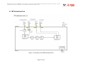
This document is a property of ESS-Bilbao. The recipient hereby acknowledges this right and
shall not without written permission give it in whole or in part to third parties or use it for any
other purposes other than those for which it was delivered to him.
Technical Report of the
ISIS LLRF
ESS-Bilbao RF group,
UPV Control Department
February 2010
Page 1 of 49
This document is a property of ESS-Bilbao. The recipient hereby acknowledges this right and
shall not without written permission give it in whole or in part to third parties or use it for any
other purposes other than those for which it was delivered to him.
Authors
Hooman Hassanzadegan
Nagore Garmendia
Supervisor
Víctor Etxebarría
e-mail address
[email protected]
[email protected]
e-mail address
[email protected]
Index
1.
2.
ISIS RFQ Specifications ............................................................................................. 5
Design description of the ISIS LLRF ......................................................................... 6
2.1. Amplitude and phase loops............................................................................... 6
2.2. Tuning loop....................................................................................................... 7
3. Implementation of the ISIS LLRF .............................................................................. 8
3.1. LLRF rack......................................................................................................... 8
3.2. Power Supply Unit............................................................................................ 9
3.3. RF Distribution Unit ....................................................................................... 10
3.4. Analog Front-End Unit ................................................................................... 12
3.5. Tuning Unit..................................................................................................... 14
3.6. Tuner Driver Unit ........................................................................................... 16
3.7. Digital Unit ..................................................................................................... 18
3.8. PC Unit ........................................................................................................... 19
3.9. Mock-up Cavity .............................................................................................. 20
4. LLRF unit schematics ............................................................................................... 20
4.1. RF Distribution Unit ....................................................................................... 21
4.2. Analog Front-End Unit ................................................................................... 22
4.3. Tuning Unit..................................................................................................... 23
4.4. Tuner Driver Unit ........................................................................................... 24
5. Unit interconnections ................................................................................................ 25
6. Implementation of the amplitude and phase regulation loops .................................. 30
7. Implementation of the tuning loop ............................................................................ 32
8. LLRF GUI (Graphical User Interface) ..................................................................... 33
8.1. LLRF parameters ............................................................................................ 36
9. Setting the LLRF Parameters .................................................................................... 40
9.1. Amplitude and phase loops: ........................................................................... 40
9.2. Tuning loop: ................................................................................................... 42
10.
FPGA programming procedure.............................................................................. 43
10.1.
Definition of the FPGA algorithm in MATLAB-Simulink ........................ 43
10.2.
Compilation................................................................................................. 45
10.3.
Inserting the cosim block into a cosim model ............................................ 47
10.4.
Programming the FPGA ............................................................................. 48
Page 2 of 49
This document is a property of ESS-Bilbao. The recipient hereby acknowledges this right and
shall not without written permission give it in whole or in part to third parties or use it for any
other purposes other than those for which it was delivered to him.
Index of Tables
Table 1: Specifications of the ISIS RFQ system ................................................................ 5
Table 2: RF Distribution Unit interconnections................................................................ 11
Table 3: Power budget estimation of the RF Distribution Unit ........................................ 11
Table 4: Input and output ports of the Analog Front–end Unit ........................................ 13
Table 5: Tuning Unit ports and their functions ................................................................. 16
Table 6: Input/output ports of the Tuner Driver Unit and their functions ........................ 18
Table 7: Resonant cavity measurements ........................................................................... 20
Table 8: Power Supply Unit Interconnections .................................................................. 25
Table 9: RF Distribution Unit Interconnections ............................................................... 26
Table 10: Analog Front End Unit Interconnections .......................................................... 27
Table 11: Tuning Unit Interconnections ........................................................................... 28
Table 12: Tuner Driver Unit Interconnections.................................................................. 29
Table 13: Amplitude and phase loop parameters .............................................................. 36
Table 14: Tuning loop parameters .................................................................................... 38
Table 15: Amplitude, phase and tuning loop parameters ................................................. 39
Page 3 of 49
This document is a property of ESS-Bilbao. The recipient hereby acknowledges this right and
shall not without written permission give it in whole or in part to third parties or use it for any
other purposes other than those for which it was delivered to him.
Abstract:
This report details the design and implementation of the LLRF system for the RFQ of the
ISIS Front End Stand. The LLRF system includes three feedback loops to regulate the
amplitude and phase of the RFQ field as well as the RFQ resonance frequency. The
design is based on a fast analog front-end for RF-baseband conversion and a model-based
Virtex-4 FPGA unit for signal processing and PI regulation. Complexity of the LLRF
timing is significantly reduced in the current design and the LLRF requirements are
fulfilled by utilizing the RF-baseband conversion method compared to the RF-IF
approach. A GUI has also been implemented in MATLAB-Simulink so that the user can
set the control parameters and monitor the read-back values while the LLRF system is
being tested. The report begins by presenting the main parameters of the ISIS RFQ and
continues by presenting the detailed design of the LLRF units as well as the Model Based
FPGA program in MATLAB-Simulink.
Page 4 of 49
This document is a property of ESS-Bilbao. The recipient hereby acknowledges this right and
shall not without written permission give it in whole or in part to third parties or use it for any
other purposes other than those for which it was delivered to him.
1. ISIS RFQ Specifications
Table 1 summarizes the specifications of the ISIS pulsed RFQ system:
Table 1: Specifications of the ISIS RFQ system
Nominal frequency
No. of LLRF systems
Amplitude stability
Phase stability
Tuning range
Unloaded Q
RF power (peak)
RF voltage
Synchronous phase
RF pulse width (min)
RF pulse width (max)
Pulse repetition rate
Ratio of the Copper to beam power
324
1
1
1
1
9000
1000
3000
0
250
2
50
5 to 1 (app.)
MHz
%
º
MHz
kW
KV
º
µs
ms
Hz
The width of the beam pulse will be shorter than the one of the RF pulse. The beam and
RF pulses are synchronized so that the beam pulse arrives right after the amplitude and
phase of the RF field in the RFQ have settled. The settling time should be less than 100
µs.
The magnitude of the cavity input power can exceed the nominal one (the higher limit is
the maximum output power of the Klystron) during the settling time to improve the time
needed to reach the nominal voltage in the cavity. Also the loop can be designed so that
the cavity voltage undergoes some oscillations before settling to improve this rise time.
The LLRF design engineer can play with these parameters to have the best performance.
The required amplitude and phase stability of the ISIS LLRF is 1º and 1% but higher
stabilities would be welcome if possible.
Page 5 of 49
This document is a property of ESS-Bilbao. The recipient hereby acknowledges this right and
shall not without written permission give it in whole or in part to third parties or use it for any
other purposes other than those for which it was delivered to him.
2. Design description of the ISIS LLRF
The LLRF system basically consists of two parts. The first part is the hardware and
FPGA program which regulates the I and Q components of the measured cavity voltage,
hence the amplitude and phase of the cavity field and the second part performs cavity
tuning to eliminate the reflected power. These two parts are explained in more details in
the following sub-sections:
2.1. Amplitude and phase loops
A simplified design of the ISIS LLRF (amplitude and phase loops) is shown in Figure 1:
Figure 1: Simplified design of the ISIS LLRF (Amplitude and phase loops)
In this design an IQ demodulator board is used to convert the measured RFQ field into
baseband I and Q (In-phase and Quadrature-phase). The resultant I and Q outputs are in
the next stage converted from differential to single ended and conditioned so that they
meet the input requirements of the two ADCs. The I and Q signals are then sampled and
fed into the FPGA board for all kinds of processing which are needed to be done on the
baseband signals, for example: rotation of the IQ vector (compensation of loop delays),
Page 6 of 49
This document is a property of ESS-Bilbao. The recipient hereby acknowledges this right and
shall not without written permission give it in whole or in part to third parties or use it for any
other purposes other than those for which it was delivered to him.
addition of fixed DC values to the I and Q inputs (compensation of DC offsets), PI
regulation and addition of feed-forward signals (compensation of predictable errors, also
for open-loop operation). At the output of the FPGA the I and Q signals are converted to
analog by the two DACs and then are fed into the IQ modulator generating the drive for
the RF amplifier. The LLRF system can be controlled and monitored by a local computer
running under MATLAB-Simulink. This option, however, is mainly intended for test
purposes. For the final installation, the LLRF system should be integrated into the global
control system of the accelerator facility.
2.2. Tuning loop
Figure 2 shows the design of the tuning loop which is also based on IQ demodulation:
Figure 2: Simplified design of the ISIS LLRF (tuning loop)
In this design, the cavity probe voltage and the forward voltage are measured by two IQ
demodulator boards and the resultant I and Q signals are sampled and fed into the digital
board which is based on a FPGA (this board is physically the same as the one used for
amplitude and phase regulation). The FPGA board calculates the phase difference
between these two RF signals and depending on its value sends the required pulse and
direction signals to the tuner driver to have the cavity matched to the klystron thus
minimize the reflected power.
Page 7 of 49
This document is a property of ESS-Bilbao. The recipient hereby acknowledges this right and
shall not without written permission give it in whole or in part to third parties or use it for any
other purposes other than those for which it was delivered to him.
The tuning loop tends to keep the phase error (i.e. the phase difference between the
forward and cavity voltages) between an upper and a lower threshold (typically a fraction
of a degree). If, for example, the measured error exceeds the upper threshold, the loop
moves the tuner in the right direction until the error becomes smaller than the upper
threshold and then leaves the tuner at that position until the next time the phase error
exceeds any of the thresholds.
In order to prevent the tuner from moving continuously in and out, tuning is done only
during the RF pulse after the phase has settled. For that purpose the tuning loop is
synchronized with the 50 Hz RF pulse rate through the FPGA program.
3. Implementation of the ISIS LLRF
3.1. LLRF rack
A 19-inch industrial rack (not part of the delivery) with a height of 2 m was used for the
installation of the low-level electronics at the UPV-EHU RF lab. This rack
accommodates the LLRF system comprising the Power Supply Unit, RF Distribution
Unit, Analog Front-end Unit, Tuning Unit, FPGA Unit and the Tuner Driver Unit. The
rest of the rack space was used for some other equipments (ex: RF generator, Laptop
computer, oscilloscope, etc) during the system development and test. Figure 3 shows the
LLRF rack with the units installed in it (the Tuner Driver Unit is not shown in the picture
but it will be part of the delivery). Each of these units is explained in more details in the
following subsections.
Page 8 of 49
This document is a property of ESS-Bilbao. The recipient hereby acknowledges this right and
shall not without written permission give it in whole or in part to third parties or use it for any
other purposes other than those for which it was delivered to him.
Power Supply Unit
Tuning Unit
FPGA Unit
Analog Front End Unit
Laptop computer for
local monitoring and
control
Mock-up Cavity
Tuner Driver Unit
RF Distribution Unit
RF Generator
(MO)
Figure 3: the LLRF rack
3.2. Power Supply Unit
The Power Supply Unit (3U) generates the required supply voltages (±5 V, +12 V) for all
the other LLRF units. These are linear type power supplies from Power-one® with very
low output noise and ripple.
Page 9 of 49
This document is a property of ESS-Bilbao. The recipient hereby acknowledges this right and
shall not without written permission give it in whole or in part to third parties or use it for any
other purposes other than those for which it was delivered to him.
Outputs
220 V
+5V
-5V
12V
Figure 4: Picture of the interior of the Power Supply Unit
The LEDs on the front panel can be used to check the status of the output voltages with
the following color code (The same color code has been used for the other units as well).
• Red LED:
+5V
• Green LED: -5V
• Yellow LED: 12V
The output voltages are distributed to the other units via the six circular connectors
mounted on the rear panel.
3.3. RF Distribution Unit
The output signal of the RF generator (Master Oscillator) is fed into the RF Distribution
Unit with a typical level of 15dBm. After frequency doubling and filtering, this unit
distributes both fRF and 2*fRF among the other units. While fRF is needed for the IQ
modulator, 2*fRF is used for the IQ demodulators included in the regulation loops or for
RF diagnostics. The components for the implementation of the RF Distribution Unit are
mainly purchased from Mini-circuits.
The schematic of this unit is shown in Figure 11.
Figure 5 shows a picture of the interior of the RF Distribution Unit:
Page 10 of 49
This document is a property of ESS-Bilbao. The recipient hereby acknowledges this right and
shall not without written permission give it in whole or in part to third parties or use it for any
other purposes other than those for which it was delivered to him.
RFin RFout 2RFout1-2
Figure 5: Picture of the RF Distribution Unit
The interconnection of the RF Distribution Unit with the other units is summarized in
Table 2:
Table 2: RF Distribution Unit interconnections
Port
Level
(dBm)
15
-2
RFin
RFout
In
/Out
input
output
2RFout-1
-7
output
2RFout-2
-7
output
Function
324 MHz ref. from the master oscillator (MO)
324 MHz reference for the IQ modulator of the Analog
Front-end Unit
648 MHz reference for the IQ demodulator of the
Analog Front-end Unit
648 MHz reference for the two IQ demodulators of the
Tuning Unit
The power budget of the RF Distribution Unit is summarized in Table 3:
Table 3: Power budget estimation of the RF Distribution Unit
Component
RFin (MO)
Gain_VLF-320
Gain_splitter1
Gain_attenuator
Gain_doubler
Gain_VLF-630
Gain_HPF
Gain_splitter2
RFout
Power
Level
15
-1
-3
-13
-13.5
-1.2
-0.4
-3
-2
Units
Comment
dBm
dB
dB
dB
dB
dB
dB
dB
dBm
Abs. max (IQ mod) = 10 dBm
Page 11 of 49
This document is a property of ESS-Bilbao. The recipient hereby acknowledges this right and
shall not without written permission give it in whole or in part to third parties or use it for any
other purposes other than those for which it was delivered to him.
2RFout1
2RFout2
-7
-7
dBm
dBm
Abs. max (IQ dem) = 10 dBm
Abs. max (IQ dem) = 10 dBm
3.4. Analog Front-End Unit
This unit includes the electronics which are needed for RF-to-baseband and baseband-toRF conversion. It’s based on an AD8348 Evaluation Board from Analog Devices® for IQ
demodulation, an in-house developed board based on AD8130 to convert the I/Q outputs
of the demodulator from differential to single-ended, another in-house developed board
based on AD8132 to convert from single-ended to differential and an AD8345 Evaluation
Board for IQ modulation. The circuit diagrams of the converter boards are included in the
schematics folder.
The complete schematic of the unit is shown in
Figure 12. The following figure shows the interior of the unit.
Gcrtl RFin REF-dem
InterREFlock RFout mod
O2
IQ Demodulator
IQ Modulator
RF amplifier
Icav
Qcav
Diferencial to Single
Ended Converter
Iact
Qact
Single Ended to Diferencial
Converter
Figure 6: Picture of the Analog Front-End Unit
Page 12 of 49
This document is a property of ESS-Bilbao. The recipient hereby acknowledges this right and
shall not without written permission give it in whole or in part to third parties or use it for any
other purposes other than those for which it was delivered to him.
The input/output ports of the Analog Front-end Unit and their functions are explained in
the next table.
Table 4: Input and output ports of the Analog Front–end Unit
Port
Level
O2
Gctrl
±5 V, 12V
0.65 V
(typ.)
0 dBm
(typ. max)
-10 dBm
RFin
REF-dem
Interlock
RFout
REF-mod
Icav
Qcav
Icav
Qcav
Iact
Qact
Iact
Qact
0V / 5 V
-10 dBm
±1.4 V
(max)
±1.4 V
(max)
±1.4 V
(max)
±1.4 V
(max)
±0.6 V
(max)
±0.6 V
(max)
±0.6 V
(max)
±0.6 V
(max)
Input/
Output
input
input
Function
Voltage supply
Gain control of the probe signal demodulator
input
Cavity probe voltage
input
input
output
input
output
RF reference signal for the demodulator. Frequency =
2*fMO
IQ mod. disable (in case of fault)
drive signal for the RF amplifier supplying the cavity
RF reference signal for the modulator. Frequency = fMO
I component of the cavity probe signal (SMA)
output
Q component of the cavity probe signal (SMA)
output
I component of the cavity probe signal (BNC)
output
Q component of the cavity probe signal (BNC)
input
I component of the cavity drive signal (SMA)
input
Q component of the cavity drive signal (SMA)
output
I component of the cavity drive signal (BNC)
output
Q component of the cavity drive signal (BNC)
The cavity probe signal (to be regulated by the LLRF) is fed into the Analog Front-end
Unit via the RFin port. A gain control input voltage should be provided for the IQ
demodulator through the Gctrl port. As an alternative, the demodulator gain can be
adjusted by the corresponding potentiometer mounted on the demodulator board and
setting the SW13 switch to the POT position. This, however, is not the preferred manner
of gain adjustment as potentiometers are in general subjected to drifts. In the current
configuration, one of the DAC channels is dedicated to gain adjustment of the IQ
demodulator. The level of the gain control voltage can be between 0.2 V and 1.2 V but
it’s normally fixed at 0.65V app. via the control computer as that gives best results in
terms of output linearity versus gain control voltage. The reference RF (f=2*fRF) for the
IQ demodulator is provided by the RF Distribution Unit with a typical level of -10 dBm.
The I and Q outputs of the IQ demodulator, after being converted from differential to
single-ended by the corresponding converter board are sent to the SMA connectors on the
Page 13 of 49
This document is a property of ESS-Bilbao. The recipient hereby acknowledges this right and
shall not without written permission give it in whole or in part to third parties or use it for any
other purposes other than those for which it was delivered to him.
front panel to be sampled and fed into the FPGA for the subsequent signal processing.
Additionally, a buffered copy of the I and Q signals is available on the BNC connectors
on the front panel so that they could be measured by an oscilloscope without disturbing
the feedback loops. The maximum swing of the I and Q signals is ±1.4 V but care should
be taken in order not to saturate the ADC inputs when these signals are fed into the FPGA
unit (the maximum input voltage of the ADCs is only ±1.25V). This can be done by
inserting appropriate attenuators on the RFin of the IQ demodulator and/or fine
adjustment of the demodulator gain about 0.65V.
The I and Q inputs of the IQ modulator (the I/Q drive signals) are fed into the
corresponding SMA connectors on the front panel with a buffered copy available on the
BNC connectors for local monitoring. The maximum voltage of the I/Q inputs is ±0.6 V
but that whole voltage range might not be used as the DACs have a more limited voltage
range (it’s only ±0.32 V). The I and Q signals are in the next stage converted from singleended to differential and fed into the IQ modulator with the RF reference being provided
by the RF Distribution Unit. Similar to the IQ demodulator, appropriate attenuators
should be placed at the RF output of the LLRF so that no LLRF signal is saturated within
the whole power range of the RF amplifier supplying the cavity. The RF output of the IQ
modulator is amplified by a ZLR-700 RF amplifier from Mini-circuits® with maximum
output power of 25dBm. However, in order to make sure that the amplifier will always
work in its linear region, some attenuators have been placed at the amplifier input;
therefore the actual output power of the Analog Front-end Unit will be less than the rated
power of the amplifier.
An additional port has been provided on the rear panel for enabling/disabling the IQ
modulator for interlock purposes with a typical turn-off time of 1.5 µs. The IQ modulator
can also be manually enabled and disabled using the corresponding switch mounted on it.
An LED on the front panel indicates whether the modulator is enabled or disabled.
3.5. Tuning Unit
Figure 7 shows a picture of the Tuning Unit.
Page 14 of 49
This document is a property of ESS-Bilbao. The recipient hereby acknowledges this right and
shall not without written permission give it in whole or in part to third parties or use it for any
other purposes other than those for which it was delivered to him.
Ref.
GcrtlGcrtlfwd Vfwd refl Vrefl
IQ Demodulator
O1
IQ Demodulator
Power Splitter
(Distribution of RF ref.)
Qfwd Ifwd Qrefl Irefl
Differencial to Single Ended Converters
Supply Voltage Distribution
and LED Control PCB
Figure 7: Picture of the Tuning Unit
This unit basically consists of two AD8348 IQ demodulator boards plus two in-housedeveloped boards, similar to the one used in the Front End Unit, to convert the
differential outputs of the IQ demodulators to single ended. The forward voltage and the
cavity reflected voltage are fed into the unit via the corresponding connectors on the rear
panel to be converted to baseband. The reference RF (2*fRF) which is provided by the RF
Distribution Unit is split into two by a power splitter in the Tuning Unit and fed into the
two boards. The I/Q outputs of the two demodulators are then converted to single-ended
by the two converter boards and made available on the corresponding SMA connectors
on the front panel to be sampled by the ADCs. The voltage range of these signals is
similar to the one of the Analog Front-end Unit. Likewise, a buffered copy of the I/Q
signals is additionally sent to the BNC connectors on the front panel for local monitoring.
The four baseband outputs of the Tuning Unit are then sampled and fed into the FPGA
running the tuning program.
Two SMA connectors are mounted on the rear panel so that the user can adjust the gain
of the IQ demodulators (the preferred voltage though is 0.65V). Alternatively, the gains
can be adjusted using the corresponding potentiometers and switches mounted on the
demodulator boards. It should be noted that while the Vfwd demodulator is needed for
the tuning loop, the Vrefl one is only used for monitoring the value of the reflected
voltage in the control computer. For that reason, in the current version of the FPGA
Page 15 of 49
This document is a property of ESS-Bilbao. The recipient hereby acknowledges this right and
shall not without written permission give it in whole or in part to third parties or use it for any
other purposes other than those for which it was delivered to him.
program, a DAC channel is dedicated to the gain adjustments of the Vfwd demodulator
but the gain of the Vrefl demodulator is manually fixed at 0.65V app. by the gain
adjustment potentiometer. The schematic of the Tuning Unit is shown in fig. 13.
The next table summarizes the input and output ports of the Tuning Unit and their
functions:
Table 5: Tuning Unit ports and their functions
Port
Level
O1
±5 V,
12V
-7 dBm
0 dBm
(typ max)
0 dBm
(typ max)
0.65 V
(typ.)
0.65 V
(typ.)
±1.4 V
(max)
±1.4 V
(max)
±1.4 V
(max)
±1.4 V
(max)
±1.4 V
(max)
±1.4 V
(max)
±1.4 V
(max)
±1.4 V
(max)
Ref
Vfwd
Vrefl
Gctrl_fwd
Gctrl_refl
Ifwd
Qfwd
Ifwd
Qfwd
Irefl
Qrefl
Irefl
Qrefl
In/
Out
input
Function
Voltage supply
input
input
RF reference for both demodulators; frequency = 2*fMO
Cavity forward voltage
input
Cavity reflected voltage
input
Gain control voltage of the Vfwd demodulator
input
Gain control voltage of the Vrefl demodulator
output
I component of the cavity forward voltage (SMA)
output
Q component of the cavity forward voltage (SMA)
output
I component of the cavity forward voltage (BNC)
output
Q component of the cavity forward voltage (BNC)
output
I component of the cavity reflected voltage (SMA)
output
Q component of the cavity reflected voltage (SMA)
output
I component of the cavity reflected voltage (BNC)
output
Q component of the cavity reflected voltage (BNC)
3.6. Tuner Driver Unit
This unit consists of the stepper motor driver for cavity tuning and an in-house-developed
board which conditions the DAC output signals (Pulse and Direction) to have TTL level
as this is required for the current driver.
Page 16 of 49
This document is a property of ESS-Bilbao. The recipient hereby acknowledges this right and
shall not without written permission give it in whole or in part to third parties or use it for any
other purposes other than those for which it was delivered to him.
The stepper motor driver is an Easy Step TM 3000 Industrial Interface from Active
Robots® (please refer to its corresponding datasheet in the datasheets folder for more
information). The stepper motor of the mockup cavity used during the LLRF tests was
Mclennan 26DBM series DLA´s.
Figure 8 shows the Tuner Driver Unit with the driver and conditioning boards mounted in
it:
Analog
IN
Pulse Direction
(TTL) (TTL)
Pulse Direction
O3
Supply voltage distribution
and LED control
TTL converter
To: Stepper motor coils
RS232: (driver reprogramming)
Stepper motor
driver
Figure 8: Picture of the Tuner Driver Unit
The pulse and direction inputs are fed into the Tuner Driver Unit via the corresponding
connectors on the rear panel. The level of these signals is fixed in the FPGA program so
that the conditioning board generates the required signal levels for the output ports and
the driver board. An analog input port is additionally foreseen so that the driver can also
work in analog input mode if needed (with the current design, though, this port is not
used). The pulse and direction signals with TTL levels are available on the corresponding
connectors on the rear panel. These signals can therefore be used if the Tuner Driver Unit
should control a stepper motor not compatible with the current driver board (in that case
only the TTL converter board of the Tuner Driver Unit will be used as the stepper motor
should be driven by another stepper motor driver). The required pulses for the stepper
motor coils are accessible via the two quick connect terminals on the front panel. Also, an
RS 232 port has been foreseen on the front panel to reprogram the driver board if needed
(please refer to the Easy Step TM 3000 Industrial Interface datasheet for details)
Table 6 shows the input and output ports of the Tuner Driver Unit and their functions:
Page 17 of 49
This document is a property of ESS-Bilbao. The recipient hereby acknowledges this right and
shall not without written permission give it in whole or in part to third parties or use it for any
other purposes other than those for which it was delivered to him.
Table 6: Input/output ports of the Tuner Driver Unit and their functions
Port
Level
O3
±5 V,
12V
0V /
0.2V
0V /
0.2V
TTL
TTL
Analog IN
Pulse
Direction
Pulse (TTL)
Direction
(TTL)
A,C,AC,
B,D,BD
RS-232
In/
Out
input
Function
Voltage supply
input
input
Not used in the current design
Pulse input for the driver board (from the Digital Unit)
input
Direction input for the driver board (from the Digital Unit)
output
output
Pulse output with TTL level
Direction output with TTL level
output
Current pulses for the stepper motor coils
input
Programming the driver board
3.7. Digital Unit
The Digital Unit includes the FPGA board and the ADC and DAC cards. This is a high
performance VHS-ADC board from Lyrtech® (with cPCI to 4x PCIe interface for PC
connection) based on a Virtex4 FPGA from Xilinx and eight AD6645 ADCs with a
resolution of 14 bits and maximum sampling rate of 105 MSPS (please refer to the
corresponding datasheets about these boards for more information). The board also
incorporates 128 MB of SDRAM for data buffering on the FPGA. In order to provide the
FPGA board with 8 additional DAC inputs, an add-on DAC module from Lyrtech was
also purchased and mounted on the FPGA board. These are DAC5687 from Texas
Instruments with a resolution of 14 bits and maximum sampling rate of 480 MSPS
(interpolating).
The FPGA was programmed using the Xilinx® System Generator and the Lyrtech®
Model Based Design Kit in the MATLAB-Simulink environment. The advantage of this
method was that the FPGA programming was eased and the time needed to develop the
FPGA code was significantly reduced compared to VHDL.
In order to further reduce the time and effort needed for the establishment of the LLRF
test bench, it was decided to co-simulate the FPGA hardware in the MATLAB-Simulink
environment. With this method, known as HIL (Hardware-In-the-Loop) co-simulation,
the FPGA communicates directly with Simulink blocks; therefore the FPGA hardware
can be tested without having to connect it to real-world signals. Then, Simulink source
blocks were used to set the LLRF input parameters (such as the PI gains and the offset
values) eliminating the need for an additional GUI (Graphical User Interface) and a
communication protocol, while the I/Q input and output signals were still the real ones
Page 18 of 49
This document is a property of ESS-Bilbao. The recipient hereby acknowledges this right and
shall not without written permission give it in whole or in part to third parties or use it for any
other purposes other than those for which it was delivered to him.
coming from the Analog Front-end Unit connected to the mockup cavity. It should be
noted, however, that although the HIL co-simulation of the loop proved to be very useful
during the system development, test and trouble-shooting, it’s not planned to use it for the
final deployment as the LLRF system should be integrated into the global control system
of the accelerator facility.
Figure 9 shows the FPGA card cage with the cPCI port, the VHS-ADC board and the
DAC module mounted in it. For information on these items, please refer to the
corresponding datasheets in the Datasheets folder.
8 DAC channels
8 ADC channels
cPCI port
Figure 9: Picture of the Digital Unit
3.8. PC Unit
A laptop computer (HP EliteBook 8530p, 2.4 GHz with 2 GB of RAM and 250 GB of
HD) was used for the development of the FPGA program and later for the LLRF tests
with the mockup cavity. As this laptop is not planned to be part of the delivery, it’s
important to consider the following requirement from Lyrtech® when a new laptop for the
LLRF system is being purchased.
The FPGA interface with the laptop might malfunction if any of these requirements
is not met:
Manufacturer:
Dell
Operating System:
Microsoft Windows XP Professional
or
Hewlett Packard (HP)
Service Pack 2
Express Card for compact PCI connection
Installation of the following software packages on the laptop is required before the FPGA
can be programmed or the HIL co-simulalation can run:
Software for BSDK:
ISE Foundation 9.2
Software for MBDK:
Matlab R2007a and System Generator for DST 9.2
Page 19 of 49
This document is a property of ESS-Bilbao. The recipient hereby acknowledges this right and
shall not without written permission give it in whole or in part to third parties or use it for any
other purposes other than those for which it was delivered to him.
For detailed information on the required software packages and the installation
procedure, please refer to the corresponding User’s Manual from Lyrtech®.
3.9. Mock-up Cavity
A mock-up cavity was designed and manufactured in order to perform the LLRF tests at
low power and validate the performance of the regulation loops. The cavity is of reentrant type to reduce the size, and is made from Aluminum except the plunger which is
made of steel. Its resonance frequency is compliant with the ISIS requirements (i.e. 324
MHz) and its quality factor was measured at 1450 approximately. The cavity was
designed by Ellyt® and manufactured by Tekniker®. Table 7 and Figure 10 summarize the
results of the cavity measurements with a Network Analyzer with the tuner moved to
both ends:
Table 7: Resonant cavity measurements
fcavity (MHz)
325.7750
326.9000
Plunger position
Completely out
Completely in
IL(dB)
-15.12
-16.15
QL
1448
1454
s21_phase (º) Cavity
s21 (dB) Cavity
180
-10
160
-15
140
120
-20
100
80
s21(º)_phase
s21(dB)
-25
-30
-35
-40
60
40
20
0
-20
-45
-40
-60
-50
-80
-100
-55
320
321
322
323
324
325
326
327
328
329
330
320
321
322
323
324
325
326
327
328
Freq (MHz)
Freq (MHz)
Figure 10: Resonant cavity S21 measurements
4.
LLRF unit schematics
Schematics of the LLRF units explained earlier are shown in the next figures:
Page 20 of 49
329
330
This document is a property of ESS-Bilbao. The recipient hereby acknowledges this right and shall not without written permission give it in whole or in part to
third parties or use it for any other purposes other than those for which it was delivered to him.
4.1. RF Distribution Unit
Figure 11: Schematic of the RF Distribution Unit
Page 21 of 49
This document is a property of ESS-Bilbao. The recipient hereby acknowledges this right and shall not without written permission give it in whole or in part to
third parties or use it for any other purposes other than those for which it was delivered to him.
4.2. Analog Front-End Unit
Figure 12: Schematic of the Analog Front-End Unit
Page 22 of 49
This document is a property of ESS-Bilbao. The recipient hereby acknowledges this right and shall not without written permission give it in whole or in part to
third parties or use it for any other purposes other than those for which it was delivered to him.
4.3. Tuning Unit
Figure 13: Schematic of the Tuning Unit
Page 23 of 49
This document is a property of ESS-Bilbao. The recipient hereby acknowledges this right and shall not without written permission give it in whole or in part to
third parties or use it for any other purposes other than those for which it was delivered to him.
4.4. Tuner Driver Unit
Figure 14: Schematic of the Tuner Driver Unit
Page 24 of 49
This document is a property of ESS-Bilbao. The recipient hereby acknowledges this right and shall not without written permission give it in whole or in part to
third parties or use it for any other purposes other than those for which it was delivered to him.
5. Unit interconnections
The interconnections among the different LLRF units are summarized in the following tables:
Table 8: Power Supply Unit Interconnections
Name
Power inlet
O1
Input/
output
input
output
Panel
Position
rear
rear
O2
output
rear
O3
output
rear
O4
O5
O6
+5 V
-5 V
+ 12 V
output
output
output
NA
NA
NA
rear
rear
rear
front
front
front
Connection
From/To Unit
Type
220 V inlet From power line
Binder 8pin To Tuning Unit (connection
with cable O1!)
Binder 8pin To Analog Front-end Unit
(connection with cable 02!)
Binder 8pin To Tuner Driver Unit
(connection with cable O3!)
Binder 8pin Spare
Binder 8pin Spare
Binder 8pin Spare
LED red
Not Applicable (NA)
LED green NA
LED yellow NA
Operating
Level
220 V
±5 V, 12 V
Abs_Max.
Rating*
±5 V, 12 V
±5.5 V
±5.5 V
±5 V, 12 V
±5 V, 12 V
±5 V, 12 V
±5 V, 12 V
On
On
On
Note:
(1) Three outputs of the Power Supply Unit are foreseen as spares in case they will be needed in the future for other units.
(2) The abs_max ratings refer to the IQ mod. and dem. boards.
Page 25 of 49
This document is a property of ESS-Bilbao. The recipient hereby acknowledges this right and shall not without written permission give it in whole or in part to
third parties or use it for any other purposes other than those for which it was delivered to him.
Table 9: RF Distribution Unit Interconnections
Name
RFin
RFout
Input/
output
input
output
Panel
Position
rear
rear
2RFout-1
output
rear
2RFout-2
output
NA
rear
front
Connection
From/To Unit
Type
SMA
From RF Signal Generator
SMA
To Ref-mod of the Analog
Front-end Unit
SMA
To Ref-dem of the Analog
Front End Unit
SMA
To Ref of the Tuning Unit
LED red
NA
Operating
Level
15 dBm
-2 dBm
Abs_Max.
Rating*
-7 dBm
10 dBm
-7 dBm
Off
10 dBm
10 dBm
** Note: These abs_max ratings refer to the IQ mod/dem boards of the Analog Front-end Unit and Tuning Unit
Page 26 of 49
This document is a property of ESS-Bilbao. The recipient hereby acknowledges this right and shall not without written permission give it in whole or in part to
third parties or use it for any other purposes other than those for which it was delivered to him.
Table 10: Analog Front End Unit Interconnections
Name
Input/
output
input
Panel
Position
rear
RFin
Ref-dem
input
input
rear
rear
Gcrtl
input
rear
Ref-mod
input
rear
Interlock
input
rear
RFout
Icav
Icav
Qcav
Qcav
Iact
output
output
output
output
output
input
rear
front
front
front
front
front
Iact
Qact
output
input
front
front
Qact
+5 V
-5 V
+12 V
output
NA
NA
NA
front
front
front
front
O2
Connection
From/To Signal Unit
Type
Binder (8 From Power Supply Unit
pin)
SMA
From cavity pickup loop
SMA
From 2RFout-1 of RF
Distribution Unit
SMA
From channel 16 of the Digital
Unit
SMA
From RFout of the RF
Distribution Unit
SMA
From interlock system
(optional)
SMA
To RF amplifier
SMA
To channel 3 of the Digital Unit
BNC
To local oscilloscope
SMA
To channel 4 of the Digital Unit
BNC
To local oscilloscope
SMA
From channel 12 of the Digital
Unit
BNC
To local oscilloscope
SMA
From channel 13 of the Digital
Unit
BNC
To local oscilloscope
LED
LED
LED
Page 27 of 49
Operating
Level
±5 V, 12 V
Abs_Max.
Rating
0 dBm (max)
-7 dBm
10 dBm
10 dBm
0.2 V–1.2 V
5.5 V
-2 dBm
10 dBm
TTL
To be set
±1.4 V (max)
±1.4 V (max)
±1.4 V (max)
±1.4 V (max)
±0.6 V (max)
±0.6 V (max)
±0.6 V (max)
±0.6 V (max)
ON
ON
ON
This document is a property of ESS-Bilbao. The recipient hereby acknowledges this right and shall not without written permission give it in whole or in part to
third parties or use it for any other purposes other than those for which it was delivered to him.
Table 11: Tuning Unit Interconnections
Name
O1
Input/
output
input
Panel
Position
rear
Ref
input
rear
Vfwd
input
rear
Gctrl-fwd
input
rear
Vrefl
input
rear
Gctrl-refl
input
rear
Ifwd
Ifwd
Qfwd
Qfwd
Irefl
Irefl
Qrefl
Qrefl
+5 V
-5 V
+12 V
output
output
output
output
output
output
output
output
rear
front
front
front
front
front
front
front
front
front
front
Connection
From/To Signal Unit
Type
Binder
From the Power Supply Unit
(8 pin)
SMA
From 2RFout-2 of the RF
Distribution Unit
SMA
From directional coupler
measuring the cavity forward
voltage
SMA
From channel 15 of the Digital
Unit
SMA
From directional coupler
measuring the cavity reflected
voltage
SMA
NA (the gain adjustment is
manual with the current
configuration)
SMA
To channel 2 of the Digital Unit
BNC
To local oscilloscope
SMA
To channel 1 of the Digital Unit
BNC
To local oscilloscope
SMA
To channel 5 of the Digital Unit
BNC
To local oscilloscope
SMA
To channel 6 of the Digital Unit
BNC
To local oscilloscope
LED
LED
NA
LED
Page 28 of 49
Operating
Level
±5 V, 12 V
Abs_Max.
Rating
-7 dBm
10 dBm
0 dBm (max)
10 dBm
0.2 V – 1.2 V
5.5 V
0 dBm (max)
10 dBm
0.2 V – 1.2 V
5.5 V
±1.4 V (max)
±1.4 V (max)
±1.4 V (max)
±1.4 V (max)
±1.4 V (max)
±1.4 V (max)
±1.4 V (max)
±1.4 V (max)
ON
ON
OFF
This document is a property of ESS-Bilbao. The recipient hereby acknowledges this right and shall not without written permission give it in whole or in part to
third parties or use it for any other purposes other than those for which it was delivered to him.
Table 12: Tuner Driver Unit Interconnections
Name
Input/
output
input
output
Panel
Position
rear
rear
Direction
TTL
Analog IN
Pulse
output
rear
SMA
input
input
rear
rear
SMA
SMA
Direction
input
rear
SMA
A
C
AC
B
D
BD
RS232
output
output
output
output
output
output
input
front
front
front
front
front
front
front
wire
wire
wire
wire
wire
wire
D type (9 pin)
front
front
front
LED
LED
LED
O3
Pulse TTL
+5 V
-5 V
+12 V
Connection
Type
Binder (8 pin)
SMA
From/To Signal Unit
From the Power Supply Unit
To final stepper motor driver
(if needed)
To final stepper motor driver
(if needed)
NA
From channel 12 of the
Digital Unit
From channel 11 of the
Digital Unit
To stepper motor
To stepper motor
To stepper motor
To stepper motor
To stepper motor
To stepper motor
To PC (only to reprogram the
driver if needed)
NA
Page 29 of 49
Operating
Level
±5 V, 12 V
TTL
TTL
Defined in
the FPGA
Defined in
the FPGA
RS 232
ON
ON
OFF
Abs_Max.
Rating
This document is a property of ESS-Bilbao. The recipient hereby acknowledges this right and shall not without written permission give it in whole or in part to
third parties or use it for any other purposes other than those for which it was delivered to him.
6. Implementation of the amplitude and phase regulation loops
The following figure shows the schematics of the FPGA program for amplitude and phase regulation:
Figure 15: Simplified schematic of the FPGA program for amplitude and phase regulation; the parameters marked as underscore
yellow are set from the control computer
Page 30 of 49
This document is a property of ESS-Bilbao. The recipient hereby acknowledges this right and
shall not without written permission give it in whole or in part to third parties or use it for any
other purposes other than those for which it was delivered to him.
As the figure shows, the measured cavity voltage (from the cavity pickup loop) is
converted to baseband by an analog IQ demodulator board which is incorporated in the
Analog Front-end Unit. The I and Q signals, after being converted from differential to
single-ended, are sampled by 14 bit ADCs running at 104 MSPS and fed into a Virtex-4
FPGA for the required signal manipulation. That includes low-pass filtering for noise
reduction, compensating the DC offsets of the IQ demodulator, baseband phase shifting,
feed-forward control and PI regulation (please refer to the Parameter Setting section for
information on how to adjust these parameters). The I and Q outputs of the FPGA are
then converted to analog by 14 bit 480 MSPS (4x interpolation) DACs and fed into the
front-end unit where they are used as the baseband inputs of the IQ modulator generating
the drive for the RF amplifier.
The magnitude and phase of the RFQ field during the pulse is controlled by setting proper
values for the Iref and Qref inputs from the control computer. The use of the feed-forward
signals (IFF and QFF) is two-folded. First, they can be used to operate the cavity in
open-loop mode (In this case, the OL/CL switch is opened; therefore the IQ modulator is
only driven by the IFF and QFF inputs). This mode can be particularly useful for test
purposes or for making sure that the regulation loops will be stable before they are
actually closed. Second, it can be used to compensate for repetitive or predictable errors
(such as the beam) before these errors are sensed and corrected by the I/Q regulation
loops.
Page 31 of 49
This document is a property of ESS-Bilbao. The recipient hereby acknowledges this right and shall not without written permission give it in whole or in part to
third parties or use it for any other purposes other than those for which it was delivered to him.
7. Implementation of the tuning loop
The following figure shows the schematics of the FPGA program for cavity tuning:
Figure 16: Simplified schematic of the FPGA program for the tuning loop
Page 32 of 49
This document is a property of ESS-Bilbao. The recipient hereby acknowledges this right and
shall not without written permission give it in whole or in part to third parties or use it for any
other purposes other than those for which it was delivered to him.
As the schematic show, the design of the tuning loop is also based on IQ demodulation.
In this case, two IQ demodulators are used to convert the cavity forward and probe
voltages to baseband (the IQ demodulator for the probe voltage is physically the same as
the one used for amplitude and phase regulation) and the resultant I/Q signals are
sampled and fed into the FPGA. Similar to the amplitude and phase loops, offset
compensation blocks and low-pass filters have been used in the FPGA for offset
compensation and noise reduction respectively (As the tuning loop is much slower than
the amplitude and phase loops, the programmed low-pass filters for the tuning loop have
a smaller bandwidth so that the noise on the base-band signals can be further reduced
hence tuning can be done with more precision). In the next stage, the phase difference
between the forward and cavity voltages is calculated by CORDIC blocks programmed in
the FPGA. Then, the tuning loop tends to keep this phase difference as close as possible
to its desired value where the desired phase is the one giving zero reflected power from
the cavity with the presence of the beam. This is done by defining two phase thresholds
(typically a fraction of a degree) above and below zero and keeping the actual phase error
always between these thresholds by moving the tuner inwards/outwards if the error
exceeds either of the thresholds. For information on how to adjust the tuning parameters,
please refer to the Parameter Setting section in this report.
In order to prevent the tuner from moving continuously inwards and outwards in pulsed
mode (that can result an early wear out of the tuner hardware) the tuning loop is only
activated during the pulse after the cavity field has settled.
8. LLRF GUI (Graphical User Interface)
As mentioned earlier, a MATLAB-Simulink GUI has been made with the cosim block so
that the LLRF system could be tested without having to integrate it into the global control
system of the accelerator facility. This GUI allows the user to set the LLRF parameters
and additionally monitor all the important parameters of the system while it’s running.
The following figure shows a snapshot of the GUI taken while the LLRF system was
running:
Page 33 of 49
This document is a property of ESS-Bilbao. The recipient hereby acknowledges this right and
shall not without written permission give it in whole or in part to third parties or use it for any
other purposes other than those for which it was delivered to him.
Figure 17: Snapshot of the LLRF GUI
Page 34 of 49
This document is a property of ESS-Bilbao. The recipient hereby acknowledges this right and
shall not without written permission give it in whole or in part to third parties or use it for any
other purposes other than those for which it was delivered to him.
The parameters on the left of the co-simulation block are the control loop parameters
while the ones on the right are the read-back values for system monitoring.
The Simulink scope blocks have been used to graphically monitor different parameters
versus time, for example: amplitude of the forward voltage, amplitude of the cavity
reflected voltage, tuner position, phase error, etc. These scope blocks can be particularly
useful when the LLRF system is put into operation during long time periods so that the
user can see a history of the data. The numerical displays show the current values of the
parameters.
The following color code has been used to easily distinguish the amp/ph blocks from
tuning blocks and common blocks:
Magenta:
Blue:
Green:
amplitude and phase loop parameters
tuning loop parameters
common parameters for the amp/ph and tuning loops
Additionally, Amph, Tu and Com prefixes and numbers have been used in front of each
parameter name in the cosim block to indicate to which category that parameter belongs.
Page 35 of 49
This document is a property of ESS-Bilbao. The recipient hereby acknowledges this right and shall not without written permission give it in whole or in part to
third parties or use it for any other purposes other than those for which it was delivered to him.
8.1. LLRF parameters
The following three tables summarize the parameters of the amp/ph loop, the tuning loop and the common parameters as well as their
function and range:
Table 13: Amplitude and phase loop parameters
Parameter
Amph_01_Iset
Amph_02_Qset
Amph_03_Pgain_cav(I)
Amph_04_Igain_cav(I)
Amph_05_Pgain_cav(Q)
Amph_06_Igain_cav(Q)
Amph_07_O.L_C.L
Amph_08_Iff
Amph_09_Qff
Amph_10_Teta_in
Amph_11_Teta_out
Amph_12_Icav_ofst_out
Function
determines the reference value for the I component of the cavity field (closed
loop mode only)
determines the reference value for the Q component of the cavity field (closed
loop mode only)
the proportional gain of the PI controller for the I component of the cavity
voltage
the integral gain of the PI controller for the I component of the cavity voltage
the proportional gain of the PI controller for the Q component of the cavity
voltage
the integral gain of the PI controller for the Q component of the cavity voltage
Changes the operation mode from open-loop to closed-loop and vice versa
determines the I component of the cavity feed-forward voltage (open-loop and
closed-loop mode)
determines the Q component of the cavity feed-forward voltage (open-loop and
closed-loop mode)
determines the rotation angle of the input phase shifter applied to the cavity
probe voltage
determines the rotation angle of the output phase shifter applied to the cavity
drive voltage
compensates the DC offset introduced by the DAC module and the IQ
modulator on the I drive signal
Page 36 of 49
Range
[-8191,8192]
[-8191,8192]
[-31,32]
[-1,2]
[-31,32]
[-1,2]
Open/
Closed
[-8191,8192]
[-8191,8192]
[-8191,8192]
[-8191,8192]
[-8191,8192]
This document is a property of ESS-Bilbao. The recipient hereby acknowledges this right and shall not without written permission give it in whole or in part to
third parties or use it for any other purposes other than those for which it was delivered to him.
Amph_13_Qcav_ofst_out
Amph_15_CW_Pulse
compensates the DC offset introduced by the DAC module and the IQ
modulator on the Q drive signal
sets the value of the demodulator gain of the cavity probe signal in the Analog
Front-end Unit
sets the operation mode of the LLRF system to CW or Pulsed
Amph_16_mag_Vin
Amph_17_ph_Vin
Amph_18_mag_Vout
displays the magnitude of the cavity probe voltage
displays the phase of the cavity probe voltage
displays the magnitude of the cavity drive voltage
Amph_14_dem_cav_gain
[-8191,8192]
[-8191,8192]
Open/
Closed
[0,8192]
[-180,+180]
[0,8192]
Note:
• The Amph_10_Teta_in and Amph_11_Teta_out are scaled in the Simulink model so that their values can be inserted in
degrees into the corresponding input boxes.
•
The Amph_14_dem_cav_gain is fed into a limiter block in the Simulink model in order not to exceed the acceptable
voltage range of the demodulator board.
Page 37 of 49
This document is a property of ESS-Bilbao. The recipient hereby acknowledges this right and shall not without written permission give it in whole or in part to
third parties or use it for any other purposes other than those for which it was delivered to him.
Table 14: Tuning loop parameters
Parameter
Tu_01_Ifwd_ofst
Tu_02_Qfwd_ofst
Tu_03_Teta_fwd
Tu_04_Teta_cav
Tu_05_Ph_err_max
Tu_06_Ph_err_min
Tu_07_Pulse_enable
Tu_08_Movement_reversal
Tu_09_Counter_reset
Tu_10_dem_fwd_gain
Tu_11_ph_Vfwd
Tu_12_ph_Vcav
Tu_13_ph_error
Tu_14_mag_Vrefl
Tu_15_Tuner_position
Tu_16_Tuner_direction
Function
compensates the DC offset introduced by the ADC module and the IQ
demodulator on the I component of the forward signal
compensates the DC offset introduced by the ADC module and the IQ
demodulator on the Q component of the forward signal
determines the rotation angle of the phase shifter applied to the cavity forward
voltage
determines the rotation angle of the phase shifter applied to the cavity probe
voltage (separate from the one used for the amp/ph loops)
sets the upper threshold for the phase error (in degrees). If the (Ph(Vprobe)Ph(Vforward)) is higher than this value the tuner moves in the correct
direction until the error becomes smaller than this threshold.
sets the lower threshold for the phase error (in degrees). If the (Ph(Vprobe)Ph(Vforward)) is lower than this value the tuner moves in the correct direction
until the error becomes larger than this threshold.
Allows the operator to enable or to disable the tuning
changes the direction of the tuner movement
resets or runs the counter which displays the positions of the tuner (in steps)
sets the gain of the demodulator for the cavity forward signal in the tuning unit
displays the phase of the cavity forward voltage in degrees
displays the phase of the cavity probe voltage in degrees
displays the difference between the cavity forward and probe voltages
displays the magnitude of the cavity reflected voltage in steps
displays the current position of the tuner
displays the direction of the tuner movement as the following:
no movement: 0
inwards / outwards: -1/1 or vice versa (depending on
Tu_08_Movement_reversal)
Page 38 of 49
Value Range
[-8191,8192]
[-8191,8192]
[-8191,8192]
[-8191,8192]
[-511,512]
[-511,512]
Enable/Disable
Rev/OK
Reset/Run
[-8191,8192]
[-180,+180]
[-180,+180]
[-360,+360]
[0,8192]
[-2047,2048]
[-1;0;+1]
This document is a property of ESS-Bilbao. The recipient hereby acknowledges this right and shall not without written permission give it in whole or in part to
third parties or use it for any other purposes other than those for which it was delivered to him.
Note:
•
The Tu_03_Teta_fwd and Tu_04_Teta_cav are scaled in the Simulink model so that their values can be inserted in degrees
into the corresponding input boxes.
•
The Tu_10_dem_fwd_gain is fed into a limiter block in the Simulink model in order not to exceed the acceptable voltage
range of the demodulator board.
The common parameters for both amp/ph and tuning (in green) are:
Table 15: Amplitude, phase and tuning loop parameters
Parameter
Com_01_Icav_ofst
Com_02_Qcav_ofst
Function
compensates the DC offset introduced by the ADC module and the IQ
demodulator on the I component of the cavity probe signal
compensates the DC offset introduced by the ADC module and the IQ
demodulator on the Q component of the cavity probe signal
Page 39 of 49
Value Range
[-8192,8192]
[-8192,8192]
This document is a property of ESS-Bilbao. The recipient hereby acknowledges this right and
shall not without written permission give it in whole or in part to third parties or use it for any
other purposes other than those for which it was delivered to him.
9. Setting the LLRF Parameters
Several LLRF parameters must be set properly before the RF system is put into operation
under power. That includes the non-negligible DC offsets of the IQ modulator and
modulators, the PI gains, the amount of the phase shifts, etc. The setting of these
parameters is done via the control computer by inserting appropriate values into the input
boxes of the cosim model. The procedure for setting the parameters is as the following.
9.1. Amplitude and phase loops:
1. Setting the gain of the input IQ demodulator: By the dem_cav_gain parameter the
user can change the IQ demodulator gain and that, in closed-loop mode, scales the
RFQ field accordingly. In open loop mode, changing this parameter will not have any
effect on the actual RFQ field but, it will scale the read-back value. It is seen that the
IQ demodulator response to gain variations is most linear when the gain value is set to
0.65 V app. (4260 steps in the cosim model). Therefore, it’s preferred to use the gain
control only around 0.65 V for fine adjustments of the RFQ power level when the
system is first configured (for coarse power level setting at system setup stage,
appropriate attenuators must be placed at the input and output of the LLRF system so
that the whole dynamic range of the system can be used while avoiding component
damage due to high signal levels). Once the optimum value of the input gain has been
found it should not be changed anymore unless the loop gain should be fine adjusted
again (ex. an attenuator value is changed the loop).
2. Offset compensation of the IQ modulator (output offset compensation): This is
necessary to ensure that when the set value for the RFQ voltage (in the control
computer) is zero, the actual field in the RFQ is also zero. In order to do the
compensation, the LLRF system must be first put into operation in open-loop mode
and the mag_Vfwd must be set to zero. Then the Icav_ofst_out and Qcav_ofst_out
should be changed manually while watching the real output power of the Front-End
Unit (RFout) using for example an RF power meter or an spectrum analyzer (this
implies disconnecting the LLRF output temporarily in order to connect it to the power
meter). In this way, right offset values are found so that the LLRF output at the RF
frequency becomes as small as possible. This is normally done after a few trials. It
should be noted that the output offset consists of two parts: these are the offset of the
IQ modulator (it can be as large as 200 mV app.) and the offset of the DAC unit
(typically a few mV only). Using the method explained earlier, the overall offset (the
sum of the two offsets) will be compensated at once.
3. Offset compensation of the IQ demodulator (input offset): This is necessary to ensure
that when the actual RFQ field is zero, the read-back value (in the control computer)
will also be zero. Input offset compensation must be done only after the output offset
was compensated (step 2). This is done by first putting the LLRF system into
Page 40 of 49
This document is a property of ESS-Bilbao. The recipient hereby acknowledges this right and
shall not without written permission give it in whole or in part to third parties or use it for any
other purposes other than those for which it was delivered to him.
operation in open-loop mode and setting the LLRF output to zero. Then the right
Icav_ofst and Qcav_ofst values are found by a few trial and errors so that the readback RFQ field (mag_Vin) is also zero.
4. Setting the phase shifts (i.e. Teta_in and Teta_out): In order to ensure that the IQ
loops will be stable before they are actually closed, the fractional part of the loop
delay must be compensated. This is done by adjusting either Teta_in or Teta_out (or
both). If, for example, the total delay from the LLRF output along the RF transmitter
and the RFQ to the LLRF and the two PI controllers is 512.3 times the RF period, the
phase shifters must be set so that the overall phase shift (i.e. the sum of the two phase
shifts) compensates 0.3 RF periods. Then the IQ vector enters at the input of the PIs
with correct phase. If the phase shift value is not properly set, the response of the I
and Q loops will not be the same and some degradations in the step response might be
seen as well. In the extreme case, if the phase error exceeds the phase margin of the
loop, the loop will become unstable (in the preliminary tests, the phase margin was
measured at ±55° about the optimum phase giving a very large margin for loop
stability). Having two phase shifters (one at the LLRF input and another one at the
output) will give the possibility to maintain the loops stable while additionally rotate
the read-back IQ vector so that the monitored phase will be the same as the actual
RFQ phase (or the phase of any RF signal along the loop path which is of interest for
the operator).
In order to find the optimum value of the phase shifts, the LLRF system must be put
into open-loop mode and mag_Vfwd is set to a non-zero value. Then either Teta_in or
Teta_out is changed so that the read-back phase of Vin is the same as the set value
(for example both are 45°). That guarantees that the I and Q loops will be stable
(assuming the PI and loop gains are not too high) and the response of both loops will
be equal provided that the other parameters of the two loops are also equal. Once the
optimum value of the phase shift is found, it should not be changed anymore unless
there’s a change in the loop delay (ex: a cable is changed) which implies finding a
new value for the phase shift(s).
5. Setting the PI gains: The PI gains for the I and Q loops are normally set to be equal.
In order to adjust the PI gains, the LLRF system should be put into operation in
closed-loop (pulsed mode). It’s important to note that improper PI gains can make the
loops oscillatory or even unstable; therefore care should be taken to avoid instabilities
when the loops are closed around the RFQ for the first time. Loop instability can be
avoided by setting the integral gain to zero and the P gain to relatively low values at
first (this implies that the real amplitude of the RF pulse will smaller than the set
value). After the loop is successfully closed, optimum P and I gains can be found by a
few trail and errors so that the loop response becomes desirable (this normally
corresponds to a response which is as fast as possible but does not undergo any
overshoot or oscillations). A simple way for gain adjustment could be the following:
first the I gain is set to zero and the P gain is set so that the real RFQ field is almost
half of the set value. Then the I gain is increased step by step until the loop response
is just about to undergo an overshoot. Once the PI controllers are properly adjusted,
Page 41 of 49
This document is a property of ESS-Bilbao. The recipient hereby acknowledges this right and
shall not without written permission give it in whole or in part to third parties or use it for any
other purposes other than those for which it was delivered to him.
the gain values should not be changed anymore unless there’s a degradation in the
step response (for example if the loop gain is changed).
9.2. Tuning loop:
The tuning loop should be disabled if the RFQ field during the pulse is too small,
because then the phase of the RF signals cannot be measured and that makes the
movement of the tuner unpredictable. Therefore, before the RFQ is powered, the
tuning loop should be disabled using the Pulse_enable switch in the cosim model. If for
any reason (such as improper setting of the tuning loop parameters) the tuner moves in
the wrong direction, the movement can be reversed by the Movement_rev switch in the
cosim model. The procedure for setting the tuning loop parameters is as the following:
1. Setting the gain of the input IQ demodulator for forward voltage measurement
(dem_fwd_gain): As this IQ demodulator is only used for phase measurement
purposes, normally its gain does not need any fine adjustment. Therefore, its gain
control input can be set to 0.65 V (i.e. 4260 in the cosim model) which is the
optimum value in terms of IQ demodulator output linearity versus gain.
2. Input offset compensation: Two IQ demodulators are needed for the tuning loop.
These are used to measure the phase of the forward and cavity voltages. As the IQ
demodulator for the cavity phase measurement is physically the same as the one used
for amplitude and phase loops, once its offset has been compensated for amp/ph
regulation (step 3 in the previous subsection) that setting will also be valid for the
tuning loop. The procedure for compensating the IQ offsets of the forward voltage is
similar: once the system is put into operation in open-loop mode, the magnitude of the
RFQ voltage is set to zero (Iff = Qff = 0), then the Ifwd_ofst and Qfwd_ofst
parameters are changed by a few trial and errors until the read-back value of the Vfwd
becomes minimum (as close as possible to zero).
3. Setting the phase shifts (i.e. Teta_fwd and Teta_cav): In the FPGA program, two
phase shifters are used for the forward and cavity voltages (they are separate from the
ones used for the amplitude and phase loops). They should be adjusted so that the
following two conditions are met simultaneously: 1) when the reflection voltage is
minimum (i.e. the cavity is properly tuned) the read-back values of the forward and
cavity phases are equal. 2) When the reflected voltage is minimum, the two read-back
phases are close to zero (that is not a restrict requirement though as any value in the
range of ±30° would also be fine provided that the two values are equal). The first
condition is necessary to make sure that regulating the phase difference at zero degree
corresponds to having minimum reflected voltage. The second condition is needed for
having enough margin to avoid any phase discontinuity (i.e. phase jump from +180°
to -180° or vice versa) even if the tuner moves from one extreme to another. Bearing
in mind that the output phase of the cordic blocks in the FPGA program changes in
Page 42 of 49
This document is a property of ESS-Bilbao. The recipient hereby acknowledges this right and
shall not without written permission give it in whole or in part to third parties or use it for any
other purposes other than those for which it was delivered to him.
the ±180° range, by meeting the second condition one can avoid any phase
discontinuity which can otherwise make the tuning loop move in the wrong direction.
4. Setting the upper and lower phase error thresholds: The tuning loop moves the tuner
only when the phase error (i.e. the difference between the forward and cavity phases)
exceeds either the upper or the lower phase error thresholds. The movement continues
until the phase error enters the (Ph_err_max, Ph_err_min) window and then the
tuning algorithm leaves the tuner at that position until the next time the error exceeds
any of the two thresholds. Setting a narrower window for the phase error means that
the cavity will be more precisely tuned (less reflected power in average), but then the
tuner will move more frequently. If the phase error window is too narrow, the tuner
will vibrate at its position due to the noise on the measured signals. In the preliminary
tests, tuner vibrations were observed with (Ph_err_max, Ph_err_min) = (+0.2°, -0.2°).
For normal operation the phase error window was set to (+0.4°, -0.4°).
10. FPGA programming procedure
Here, we briefly explain the different steps which should be followed each time the
FPGA should be reprogrammed and/or the control algorithm has to be modified. For
detailed information on how to program the FPGA, please refer to the corresponding
user’s manual from Lyrtech and Xilinx.
10.1.
Definition of the FPGA algorithm in MATLAB-Simulink
As mentioned earlier, with model-based approach, the FPGA is programmed in the
MATLAB-Simulink environment. The algorithm for the regulation loops is therefore
defined using appropriate blocks from the Lyrtech, and Xilinx libraries. This option also
allows the user to perform simulations and timing analysis in order to identify errors in
the control algorithms and check the control system viability before compiling the
program.
We use the word “LLRF” for naming the FPGA source program in MATLAB-Simulink
followed by its version. For example LLRF1V2.mdl refers to version 1.2 of the program.
The following figures show the top-level FPGA program containing two main blocks for
the amp/ph and tuning loops:
Page 43 of 49
This document is a property of ESS-Bilbao. The recipient hereby acknowledges this right and
shall not without written permission give it in whole or in part to third parties or use it for any
other purposes other than those for which it was delivered to him.
Figure 18: Top level view of the FPGA program
Figure 19 and 20 show the design of the FPGA program for amp/ph regulation and tuning
with more details (yellow boxes are programmed in-house):
Figure 19: Design of the FPGA program for the amp/phase loops
Page 44 of 49
This document is a property of ESS-Bilbao. The recipient hereby acknowledges this right and
shall not without written permission give it in whole or in part to third parties or use it for any
other purposes other than those for which it was delivered to him.
Figure 20: Design of the FPGA program for the tuning loop
10.2.
Compilation
Once the FPGA program has been defined and successfully tested in MATLABSimulink, the program has to be complied to create the cosim block. This is done by
double clicking the System Generator Block in the .mdl program and choosing the
options that correspond to the actual hardware and parameters being used as shown in
Figures 21 and 22.
Figure 21: System Generator block
Page 45 of 49
This document is a property of ESS-Bilbao. The recipient hereby acknowledges this right and
shall not without written permission give it in whole or in part to third parties or use it for any
other purposes other than those for which it was delivered to him.
Figure 22: System Generator and FPGA configuration windows
The compilation starts by clicking the Generate button. Depending on the program size
and complexity, it can take several minutes or more until the compilation is finished. The
compilation will stop before finishing if the System Generator finds any unresolved error
in the FPGA program. If that happens, the user can refer to the error log file generated
during compilation so that the error can be identified and removed before starting a new
compilation.
If the compilation finishes successfully, a new window appears with the co-simulation
block automatically named as the program name followed by “hw_cosim_lib.mdl” as
shown in Figure 23. The cosim block can then be saved in the cosim library to be used in
the cosim model.
This co-simulation block contains all the input ports defined in the FPGA program as
well as the output parameters to be monitored either numerically or graphically in the
cosim model.
Page 46 of 49
This document is a property of ESS-Bilbao. The recipient hereby acknowledges this right and
shall not without written permission give it in whole or in part to third parties or use it for any
other purposes other than those for which it was delivered to him.
Figure 23: The co-simulation block
10.3.
Inserting the cosim block into a cosim model
In order to define the input values and output displays for the cosim block, another
MATLAB-Simulink file will be needed. This file is named as the original program file
followed by “_cosim.mdl”. Then, the cosim block can be inserted into the _cosim.mdl
file together with all other MATLAB-Simulink blocks which are needed to define the
inputs and outputs or further manipulate the data if needed. This, in fact, will be the GUI
that the user should work with during the HIL co-simulation (please refer to Figure 17 for
a snapshot of the GUI).
If any modification is made in the loop design, a new co-simulation block has to be
created and that implies new compilation of the design file. Then, the operator has to
substitute the old co-simulation block by the new one in the final _cosim.mdl file and
readjust the input parameters if necessary.
Page 47 of 49
This document is a property of ESS-Bilbao. The recipient hereby acknowledges this right and
shall not without written permission give it in whole or in part to third parties or use it for any
other purposes other than those for which it was delivered to him.
10.4.
Programming the FPGA
Having the cosim block inserted into the cosim model and the input and output variables
properly connected to Simulink source and sink blocks, the user can now run the
_cosim.mdl file to start the HIL co-simulation. In this model, the user can set the values
of all the loop parameters and monitor the system while it’s running.
Next, the operator has to select the bitstream file to program the FPGA. This is done by
clicking the play button in the _cosim.mdl model, as shows in Figure 24. The pop-up
window of Figure 25 will then appear where the user should select the corresponding
_cw.bit (bitstream) file which is also generated during the compilation process and saved
in the current folder. This file includes the complied logics to be implemented on the
FPGA.
Afterwards, the operator should click the Program FPGA… button to start the FPGA
programming (During the programming, four LEDs of the digital module will
illuminate). Having the FPGA programmed the “Proceed” button of the pop-up window
should be clicked to start the co-simulation.
Figure 24: Programming the FPGA using the play button
Page 48 of 49
This document is a property of ESS-Bilbao. The recipient hereby acknowledges this right and
shall not without written permission give it in whole or in part to third parties or use it for any
other purposes other than those for which it was delivered to him.
Figure 25: FPGA programming pop-up window
Please note that recompiling the FPGA program is only needed if for any reason the
FPGA algorithm should be modified (steps 1, 2 and 3). The FPGA, however, needs to be
reprogrammed each time the co-simulation is stopped or the FPGA unit is switched off
(step 4).
END OF DOCUMENT
Page 49 of 49