1
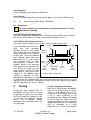
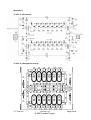
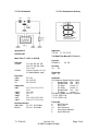
Cumbria Designs T-1
SSB/CW Filter kit (4.9152MHz)
User Manual
CONTENTS
1
INTRODUCTION
2
2
CIRCUIT DESCRIPTION
2
3
ASSEMBLY
2
4
TESTING
4
The Steading
Stainton
PENRITH
Cumbria
CA11 0ES
UK
1 Introduction
This document describes the assembly and installation method of the T-1 SSB/CW
filter kit. Please refer to the T-1 User Manual for general information regarding
component identification, placement and soldering technique.
2 Circuit Description
The T-1 Filter kit comprises of two filter
assemblies; the dual filter board and
the tail end filter board. Each board is
designed to be plugged onto headers
on the T-1 main board allowing
different filter or IF schemes to be
easily implemented by the user. The
filter crystals supplied with this kit have
been matched to within +/-10Hz to
provide reproducible filter performance
results. Three crystals have been
marked with self adhesive paper
“spots”. These crystals are for use with
the T-1 carrier oscillators and should
not be used in the filters.
2.1 Dual Filter Board
The Dual Filter board accommodates
two 6 pole ladder filters each of which
is selectable by diode switching under
control of the T-1 Control interface.
The filter components supplied in this
kit provide two filters, a Cohn SSB
filter approximately 2.5kHz bandwidth
and a Butterworth CW filter of
approximately 480Hz bandwidth. Each
of these filters defines the IF
bandwidth of the T-1. The filters are
matched to the 50 Ohm impedance of
the T-1 filter ports by ferrite
transformers. The transformers also
form part of the diode switches used to
select either filter. To offer good IMD
performance PIN diodes are used on
the wideband port (mixer side) of the
filters whereas fast switching diodes
are used on the IF side of the filters.
The Dual Filter PCB has been
designed to allow different types of
filter to be used, for the filters
described in this kit, some of the
capacitor positions are not used or
a fitted with shorting links. Please
follow the assembly instructions
carefully.
2.2 Tail End Filter
The wideband IF of the T-1 is
designed to be low noise, however
due to the gain of the IF stages the
noise component of the IF is
noticeable particularly during weak
signal reception. A simple two pole
“Tail End” filter greatly reduces the
demodulated
noise
level
by
attenuating the unwanted sideband
immediately before the IF signal is
presented to the demodulator. This
filter has a nominal bandwidth of about
2.5kHz.
3 Assembly
The following assembly sequence is recommended.
3.1
Dual Filter Board
3.1.1 Crystals
Carefully fit and solder each of the filter crystals into the positions marked on the
PCB. Exposed pads have been provided on the top side of the PCB to allow the
crystal cans to be soldered to ground. This reduces the effect of stray capacitance on
the filter performance. Take great care when soldering the cans not to overheat the
crystals. An alternative grounding technique which will probably place less stress on
the crystals is to use short lengths of tinned wire to connect the pad to the top of the
crystal can.
T-1 Filter Kit
Version 1.0
© 2005 Cumbria Designs
Page 2 of 8
3.1.2 Decoupling Capacitors
Insert leads into PCB such that the capacitor body is flush with the board surface.
Bend the leads outwards slightly to hold the capacitor in place during soldering. Trim
off excess leads.
3.1.3 Resistors
All resistors are mounted horizontally. Insert leads into the board and ensure that
resistor body is flush with PCB. Solder and trim off excess leads.
3.1.4 Filter Capacitors
a.)
All of the filter capacitors are 39pF. Note the positions!!
!
b.)
!
SSB Filter (Position A)
CW Filter (Position B)
Capacitor values vary with position in filter circuit. Take care to match value
to silk screen marking on PCB!
3.1.5 Diodes
a.) PIN Diodes
Fit the two PIN diodes (clear glass body) in positions D1 and D2. Note
orientation, cathode (band) goes towards centre.
b.) Switching Diodes
Fit the two BAV21 switching diodes in positions D3 and D4. Note orientation, cathode
(band) goes towards centre.
3.1.6 Links
Use discarded component leads to make links for positions C1, C2, C8 and C9.
3.1.7 Transformers
!
Wind matching transformers for each filter as described in the table below. Be
sure to observe the correct orientation when installing!
T1, T2
T3, T4
Primary (50 Ohm Port)
5 turns
4 turns
Secondary (Filter side)
16 turns
16 turns
3.2 Tail End Filter
The Tail End filter board is very simple to assemble.
3.2.1 Crystals
Fit the two crystals in the positions marked on the PCB in the same manner as
described in 3.1.1
T-1 Filter Kit
Version 1.0
© 2005 Cumbria Designs
Page 3 of 8
3.2.2 Capacitor
Fit the single 33pF filter capacitor in position C1.
3.2.3 Resistor
Fit R1 in the marked position ensuring that the body is flush with the PCB surface.
R1
3.3
!
1K
Brown, Black, Black, Brown, (BROWN)
Connectors
To ensure alignment, the filter boards and mounted onto the T-1 main
board before soldering.
3.3.1 Main Filter Board Connectors
With a fine bladed sharp modelling knife, cut the SIL socket and pin strips to make a
four way pin and socket for JP1 and a two way pin and socket for JP2.
3.3.2 Tail End Filter Board Connector
Cut the SIL socket and pin strips to make a 4 way pin and socket for PL1
T-1 PCB
Filter PCB
Insert the broad ends of the pin
strips
into
filter
connector
positions on the T-1 main board M2.5x16
and carefully push the matching Screw
socket strip onto the thin ends of
the pin strips. Using the hardware
pack supplied, mount each filter
board onto the T-1 main board.
M2.5
The assembly order for each
Nut
mounting point is shown in the
diagram. Some of the mounting
8mm
holes are close to live pads on the
M2.5
M2.5 Nylon
M2.5
Spacer
Steel
Washer
Steel
main PCB in the areas the post
Washer
Washer
(See text)
mixer amplifier and the IF stage
diode chain. 6 nylon washers are
Hardware Kit Assembly Detail
supplied to be applied where
isolation is required. The filter
board ground connections are already made via the connectors. The boards should
sit square with the sandwiched pin and socket connectors pushed fully home. Check
alignment of the connectors and solder into place on the top side of the filter board
and the underside of the main T-1 board.
4
Testing
Perform the initial testing of the T-1
described in the user manual. It should
be possible to switch filters by taking
the Filter A and Filter B controls on the
T-1 interface high. Doing this forward
biases
the
respective
diodes
connecting the associated filter into
the signal path.
T-1 Filter Kit
4.1 Filter Shape and Passband
Both filters should display bandwidths
close to the design values of 2.5kHz
(Filter A) and 450Hz (Filter B). A
characteristic of the ladder filter is that
it has a slight asymmetry of the
passband with the steepest skirt being
on the HF side. This implies that LSB
operation provides the best unwanted
sideband performance, this asymmetry
may be noticeable as a slight
difference in the “sound” of the receive
Version 1.0
© 2005 Cumbria Designs
Page 4 of 8
noise spectrum when switching
between LSB and USB. However, with
6 crystals the asymmetry whilst
noticeable is not too marked and good
performance on both LSB and USB
should be seen.
The filters may be fine tune by padding
out the capacitor values with small
value capacitors. Also the termination
resistance will affect the filter
response. Generally, reducing the
termination impedance or increasing
the
capacitor
values
reduces
bandwidth, increasing the termination
impedance and reducing capacitor
values increases bandwidth. There are
a number of excellent resources on
the internet and articles in ARRL and
RSGB publications describing crystal
filter design. The T-1 provides an
excellent test bed for experimentation.
4.2 Troubleshooting
4.2.1 Filter Selection Doesn’t Work
•
•
Check that the filter selection
voltage on the T-1 interface is
greater than 2V.
Check that the DC switch on
the T-1 board associated with
T-1 Filter Kit
•
•
the filter is switching on +12V
to the filter board select pin.
Check that the diodes are
biased on – is the orientation
correct?
Check that there is a complete
circuit from the select pin,
through the diode switch to
ground for the control current.
4.2.2 Filter Response is Wrong
•
•
•
Have you adjusted carrier
oscillators
for
optimum
USB/LSB operation?
Check that the impedance
matching transformers are
correctly would and installed
the right way round.
Check the capacitor values and
the positions, remember not all
of the available positions are
used for the filters described.
4.2.3 H E L P!
Still have a problem that you can’t
resolve? Don’t worry contact us by
letter
or
email
at
[email protected]
for
assistance.
Version 1.0
© 2005 Cumbria Designs
Page 5 of 8
Appendix A
T1-2FL v1.0 Schematic
T1-2FL v1.0 Component 0verlay
T-1 Filter Kit
Version 1.0
© 2005 Cumbria Designs
Page 6 of 8
T-1 FL2 Schematic
T-1 FL2 Component Overlay
Appendix B
Inductors
T37-43 T1, T2, T3, T4
PARTS LIST
Main Filter T-1 2FL v1.0 PCB
Crystals
HC49U
HC49U
Resistors
220R
560R
1K
Capacitors
39pF
100pF
180pF
220pF
10nF
100nF
Q1, Q2, Q3, Q4, Q5,
Q6, Q7, Q8, Q9, Q10,
Q11, Q12
Carrier Crystals X1, X2,
X3 (Identified by spot)
R7, R8
R1, R3, R5
R2, R4, R6
C11, C12, C13, C14,
C15
C4, C23
C5, C7
C6
C21, C22, C25, C26
C16, C17, C18, C19
Semiconductors
5802-3081
D1, D2 Pin Diodes
BAV21
D3, D4 Si Diodes
T-1 Filter Kit
Tail End Filter Board T1-FL2 v1.0
Crystals
HC49U-V
Q1, Q2
Resistor
1K
R1
Capacitor
33pF C1
Hardware
Pin Strip and Socket Strip to make;
1
Socket Strip 1X2 SK2
1
Socket Strip 1X4 SK1
1
Pin Strip
1x2 for T-1
1
Pin Strip
1x4 for T-1
1
Socket Strip 1x4
PL1
1
Pin Strip
1x4 for T-1
0.315mm Copper Wire for Inductors
T-1 2FL PCB v1.0
T-1 FL2 PCB v1.0
Fixing Kit
6
M2.5 Screws
6
M2.5 Nuts
12
M2.5 Washers
6
8mm Nylon Spacers
6
Nylon Washers
Version 1.0
© 2005 Cumbria Designs
Page 7 of 8
NOTES
T-1 Filter Kit
Version 1.0
© 2005 Cumbria Designs
Page 8 of 8