1
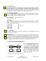
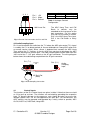
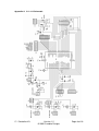
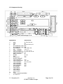
Cumbria Designs T-1
C-1 Controller
User Manual
CONTENTS
1
INTRODUCTION
2
2
CIRCUIT DESCRIPTION
2
3
ASSEMBLY
3
4
CONNECTIONS AND CONFIGURATION
4
5
TESTING
6
Appendix A C-1 Circuit Diagram and PCB Component Overlay
Appendix B Parts List
The Steading
Stainton
PENRITH
Cumbria
CA11 0ES
UK
1 Introduction
This document describes the assembly and operation of the C-1 Controller kit.
Please refer to the T-1 User Manual for general information regarding component
identification, placement and soldering technique.
2 Circuit Description
The C-1 kit is a 16F877 based
controller for the T-1 SSB/CW
Transceiver Sub-System. The C-1
produces the T/R sequencing for the
T-1 signal and power controls,
provides Hang AGC, adjustable Full
Break In CW functionality and
presents user control inputs in a
convenient and easily interfaced
format.
The C-1 connects to the T-1 by a
ready assembled, 16 way ribbon cable
assembly. An additional pair of wires is
used to extend audio from the T-1 to
the C-1 audio port for Hang AGC
operation.
The heart of the C-1 is the Microchip
PIC16F877-A processor (IC2). This
holds the firmware that interprets the
user controls to produce command
signals to condition the T-1 interface.
PORTB of IC2 is used for control
inputs. These are presented on 8 way
header PL2. The controls are held
high by the 10K resistor network RN1,
this provides a ”stronger” reference
than PORTB’s internal weak pull up
resistors. The controls are activated by
grounding the respective PL2 pins.
Care should be taken to ensure that
no potentials greater than 5V are
applied to the control inputs as this
may damage the processor.
Four analogue inputs are presented on
connectors PL3, PL4, PL5 and PL8. Of
these, three are used in the first
software version to support Hang AGC
(PL3 and PL4) and CW Break In Delay
(PL5). The fourth analogue input on
PL8 is reserved for future use.
Two of the three active analogue ports
are used to sense the voltages set by
C-1 Controller Kit
potentiometers to define AGC Hang
time (PL3) and Break In Delay (PL5).
The third active analogue input (PL4),
is an audio sampling input taken from
output of the AF pre-amplifier on the T1. Three on-board trimpots allow
preset adjustment of hang times
associated with Hang AGC (VR1), Full
Break delay (VR3) and audio input
level (VR2). As an option, the on board
pots VR1 and VR3 can be disabled
and
replaced
by
front
panel
potentiometers, connected to PL3 and
PL5, by simply re-configuring the
selection links JP1 and JP2.
The outputs used to drive the T-1
control interface, are taken from
PORTC and PORTD of the 16F877.
These are extended to the 8x2 way
MIL16 connector PL6. Pins 15 and 16
of PL6 are used to carry +12V from
the T-1 to provide power to the C-1. In
this application the optional +12V
connection point on the C-1 PCB is not
used. Bits 6 and 7 of PORTC are used
to drive Power FETs Q1 and Q2. Both
FETs are configured to provide open
drain outputs on PL1 suitable for
driving small relays or logic to operate
power amplifier change over. Q1 is
turned on when the TR sequence is
changes to Transmit, Q2 when the
sequence changes to Receive.
Spare pins on PORTA and the 3 bit
PORTE are extended on connectors
PL8 and PL7 respectively to support
future applications.
Version 1.2
© 2005 Cumbria Designs
Page 2 of 10
3 Assembly
The following assembly sequence is ordered by component height. This allows the
components to be held in place firmly in place when the PCB is turned over for
soldering.
!
3.1
IC Socket and SIL Sockets
a) Install and solder the 40 way IC socket for IC2 taking care to observe the
orientation marked on the PCB.
b) Using a sharp modelling knife, cut the socket strip into two 3 way lengths.
Insert and solder these into positions JP1 and JP2.
!
!
3.2 SIL Resistors
Insert resistor networks RN1 and RN2 taking great care to ensure correct orientation.
The black dot marking pin 1 on the SIL package must align with the pin 1 marking on
the PCB. Invert PCB and solder. Solder one end pin and check seating and
alignment of SIL package before soldering remaining pins.
3.3 Crystal
Insert the 20MHz crystal X1 and turn PCB over for soldering. The components
mounted so far will ensure that a small gap exists between the crystal and the PCB.
The extra lead length reduces thermal stress during soldering. Solder one lead,
check position and solder second lead.
3.4
1
2
!
Ceramic Capacitors
Insert and solder 22pF (22J) capacitors C10 and C11.
Insert and solder 100nF (104) C1, C6, C7, C8 and C12. Note that once
installed inside the 40 way IC socket, C8 is carefully folder flat against the
PCB.
3.5 Power FETs
Insert Q1 and Q2 in the marked positions ensuring correct orientation. Solder centre
lead to hold devices in place. Check and if necessary adjust position before soldering
remaining leads.
3.6 Resistors
Insert resistors bend leads slightly to hold in place, solder and trim off excess leads.
Tolerance band colour is given on capitals.
220R R1, R2, R8, R10
470R R9
10K R3, R4, R5, R6, R7
Red, Red, Black, Black, (BROWN)
Yellow, Mauve, Black, Black, (BROWN)
Brown, Black, Black, Red, (BROWN)
3.7 Variable Resistors
The pre-formed leads will require to be straightened to allow the potentiometers to
be inserted into the board.
One at a time, insert and solder VR1, VR2 and VR3 checking seating and position
after first lead is soldered and re-aligning if necessary before remaining pins are
soldered.
C-1 Controller Kit
Version 1.2
© 2005 Cumbria Designs
Page 3 of 10
!
!
3.8 MIL-16 Header
Insert the 8x2 way header in position PL7. Be sure to match orientation of header
with board markings. Pin 1 of the header is marked by an arrow head on the side
face of the body. This is positioned towards Q2 on the PCB such that the cut out on
the connector face matches that marked on the PCB. Once positioning has been
checked and ensuring that connector is fully seated, solder in place.
3.9 Electrolytic Capacitors
Insert electrolytic capacitors ensuring correct orientation, solder and trim off excess
leads. The negative lead is marked by a stripe on the capacitor body. The Positive
lead must match the positive marking on the PCB.
10uF Electrolytic
100uF Electrolytic
C3, C4, C5, C9, C12
C2
3.10 Headers
Insert the header connectors with the locking tabs facing the centre of the PCB.
Solder a single central pin, check alignment and seating and adjust if necessary
before soldering remaining pins.
1 Way Header
3 Way Header
4 Way Header
6 Way Header
8 Way Header
!
!
PL4
PL3, PL5, PL8
PL1
PL9
PL2
3.11 Regulator
Insert the 5v regulator IC1, ensuring correct orientation. The underside of the metal
tab should face C2 and C3.
3.11 Processor
Carefully form the pins of the 16F877 processor so that they align with the holes of
the 40 way IC socket. This is easily done by holding the processor on it’s side against
a flat surface and applying gentle pressure to bend the pins inwards. Repeat for both
sides until alignment is achieved. Take great care during insertion to ensure that all
pins engage the socket and do not become bent or folded under the device.
4 Connections and Configuration
4.1
3 2 1
JP1
C6
VR1
VR2
3 2 1
JP2
VR3
Analogue Controls Selection
The only configuration options on the
C-1 are links JP1 and JP2 which select
the on-board or external potentiometer
connections for the AGC Hang Time
and CW Break In Delay respectively.
The links are made by forming a short
length on discarded component lead
into a small “U” link. The selection
options are shown below.
Fig. 1 Analogue Control Selection Jumpers
C-1 Controller Kit
Version 1.2
© 2005 Cumbria Designs
Page 4 of 10
3 2 1
Pin 1 +5V
Pin 2 Wiper
Pin 3 Ground
10K Linear Pot
Fig. 2 External Pot Connections for PL3 and PL5
Jumper
2-3
JP1
VR1 Active
JP2
VR3 Active
1-2
External Input
External Input
Table 1 Analogue Controls
Configuration
The AGC Hang Time and CW
Break In controls may be
extended to the front panel of the
host transceiver. For this option
PL3 and PL5 are wired as shown.
PL3 is the AGC Hang Time input,
PL5 is the CW Break In Delay
input.
4.2 Audio Sampling Input
PL4 I used to monitor the audio from the T-1 before the AGC gain control. This signal
is used by the C-1 to detect periods of silence attributable to strong AGC action with
no current receive signal. When silence is detected that exceeds the AGC Hang
Time setting, the C-1 switches in the fast AGC time constant to discharge the AGC
capacitor and increase receiver gain. The audio sampling point can be taken from the
“hot” end of the T-1 AF gain control or the AF gain connector. The wiring diagram
below shows the audio being sampled from the AF gain connector.
PL1 (T-1)
Locking
Tab
PL4 (C-1)
Audio
Sampling
Input
AF Gain Pot
(Rear)
Fig. 3 Audio Sampling Connection
4.1
Control Inputs
The functions of the PL2 Control Inputs are given in table 2. Note that these are held
at +5v by pull up resistors. The functions are activated by grounding the respective
input. To prevent damage to the processor, care should be taken to ensure that
voltages greater than +5v are not applied to the input pins. For convenience, the
AGC controls may be grouped and operated by a rotary switch to provide; AGC
On/Off, AGC Fast, AGC Slow, Hang AGC.
C-1 Controller Kit
Version 1.2
© 2005 Cumbria Designs
Page 5 of 10
PL2 Pin
Number
8
7
6
5
4
3
2
1
Function
High
Low
Mute
Mode
Bandwidth
PTT/Key
AGC
AGC Speed
AGC Mode
USB/LSB
Receiver active
SSB
Filter Wide (SSB)
Receive
AGC On
AGC Fast
AGC Normal
USB
Receiver Mute
CW
Filter Narrow (CW)
Transmit
AGC Off
AGC Slow
AGC Hang
LSB
4.2 T-1 Interface
Connection to the T-1 is made by the 16 way ribbon cable assembly. This is indexed
to ensure correct orientation. The command signals on the interface are described in
the T-1 manual.
4.3 Tx/Rx Auxiliary Outputs
Two pairs of output signals to support operation of the host transceiver’s transmit and
receive switching, are presented on PL1. Each pair comprises of a TTL level signal at
zero volts for “OFF” and +5v for “ON” and an open drain power FET driven by the
associated logic signal. The Power FETs are intended to drive small relays or LED
indicators. A small delay is provided between the Tx and Rx signal state changes.
PL1 Pin
Number
1
2
3
4
Function
High
Low
Tx TTL Output
Tx FET Output
Rx TTL Output
Rx FET Output
Transmit State
Receive State
Receive State
Transmit State
5 Testing
5.1
Power
With the C-1 connected to the T-1 via the ribbon cable power on the T-1. After about
a second the T-1 should become active. If nothing happens check that the C-1 is
receiving +12v over the ribbon cable and confirm that the regulator is supplying +5v
to the processor. If there is power but the C-1 still doesn’t function, check the
placement and soldering of the clock components X1, C9, C10 and R9. Confirm that
all of the processor IC socket pins are soldered.
5.2
Functions
Test the functions by consecutively grounding each of the control input pins on PL2.
Confirm that the T-1 responds with the expected function. If a function cannot be
enabled, check the soldering of the multiway “MIL-16” connectors on the T-1 and C-1
and verify continuity from the respective processor pin through the ribbon cable to the
T-1 control circuitry.
5.3
Adjustments
5.3.1 AGC Hang Time. With the T-1 in receive and AGC on and set to Hang
operation, set the C-1 Audio Level pot VR2, fully clockwise. Using either VR1 or an
C-1 Controller Kit
Version 1.2
© 2005 Cumbria Designs
Page 6 of 10
external potentiometer connected to PL3, adjust the AGC Hang Time such that when
receiving a strong signal the AGC action remains slow between words and during
brief pauses in speech or CW but returns to maximum gain at the end of
transmission. Turning the pot clockwise increases the delay, anticlockwise reduces
the delay. With the receiver tuned to a clear frequency turn the audio level pot (VR2)
anticlockwise to the threshold of frequent triggering which can be observed by
monitoring the AGC Fast control output on pin 14 of the processor IC2. Advance VR2
clockwise slightly to reduce false triggering and obtain good Hang operation
sensitivity when receiving a signal.
5.3.2 CW Break In Time. With CW mode selected key the PTT/Key line of the C-1
and using either VR3 or an external potentiometer connected to PL5, adjust the CW
Break In Delay. Clockwise increases the delay, anticlockwise reduces the delay.
The testing of the C-1 Controller is now complete.
C-1 Controller Kit
Version 1.2
© 2005 Cumbria Designs
Page 7 of 10
Appendix A C-1 v1.0 Schematic
C-1 Controller Kit
Version 1.2
© 2005 Cumbria Designs
Page 8 of 10
C-1 Component 0verlay
Appendix B
4
1
5
1
1
3
2
4
5
1
1
2
1
1
1
1
2
3
1
1
1
1
1
2
1
1
20
1
1
PARTS LIST
220R
R1, R2, R8, R10
470R
R9
10K
R3, R4, R5, R6, R7
SIL NETWORK 8x10K RN1
SIL NETWORK 5x10K RN2
10K TRIMPOT
VR1, VR2, VR3
22pF CERAMIC
C10, C11
100nF CERAMIC
C1, C6, C7, C8
10uF ELECTROLYTIC C3, C4, C5, C9, C12
100uF ELETROLYTIC C2
20MHz CRYSTAL
X1
2N7000
Q1, Q2
7805
IC1
PIC16F877-A
IC2
40 PIN IC SOCKET
2 WAY HEADER
PL4
3 WAY PINSOCKET
JP1, JP2
3 WAY HEADER
PL3, PL5, PL8
4 WAY HEADER
PL1
6 WAY HEADER
PL9
8 WAY HEADER
PL2
8x2 HEADER
PL7
2 WAY SHELL
3 WAY SHELL
4 WAY SHELL
8 WAY SHELL
PINS
16 WAY RIBBON ASSEMBLY
C-1 PCB V1.0
C-1 Controller Kit
Version 1.2
© 2005 Cumbria Designs
Page 9 of 10
Notes
C-1 Controller Kit
Version 1.2
© 2005 Cumbria Designs
Page 10 of 10