1
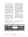
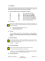
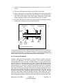
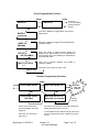
Minicounter
User Manual
CONTENTS
1
INTRODUCTION
2
2
PREPARATION
2
3
CIRCUIT DESCRIPTION
3
4
ASSEMBLY
5
5
TESTING
9
6
USER SET UP
10
7
USE
12
APPENDIX A
Troubleshooting
The Steading
Stainton
PENRITH
Cumbria
CA11 0ES
UK
1 Introduction
Thank you for purchasing the Cumbria Designs Minicounter Module. We hope
that you enjoy constructing this kit and find many uses for this feature rich design.
This manual describes the assembly and operation of the Minicounter, even if
you are a seasoned constructor, we respectfully ask that you read this manual
and familiarise yourself with the instructions and kit contents before commencing
construction. If assembled carefully, this unit will provide many years of reliable
service.
The Cumbria Designs Team
________________________________________________________________
2 Preparation
2.1
Tools
We recommend that the following
tools are used during assembly
and testing;
25W fine tipped soldering
60/40 Rosin cored solder
5” or smaller diagonal side cutters
Solder sucker (just in case!)
Multimeter
Conventions
The following symbols are used
within the assembly instructions to
draw attention to critical steps such
as component orientation and antistatic precautions. The associated
narrative describes the action
required.
!
Critical Step
Assembly
The production of a successful
finished working kit is dependent upon
care during component handling,
Minicounter v3.0 PCB1.1
Component Identification
To simplify component identification,
the parts list carries the identities of
each component as it appears on the
device. For resistors the colour coding
is given. This should be referred to
during assembly to ensure the right
parts are placed in their respective
positions on the PCB.
2.5
Static Sensitive
2.3
2.4
All parts carry a coded identity to
describe their values. It is important to
be able to recognise these during
assembly. Capacitors have their value
printed numerically, e.g. 104 = 100nF,
103 = 10nF etc. Resistors have their
values represented by coloured bands.
Small pointed nosed pliers
2.2
placement and good soldering! Don’t
be tempted to rush the construction,
even though this is a relatively simple
kit, a wrongly placed component can
provide hours of frustrating fault
finding. Also, as this kit uses a double
sided Printed Circuit Board (PCB) with
through plating, removal of a wrongly
soldered part can be difficult. Follow
the assembly instructions carefully to
avoid mistakes.
Component Leads
Many of the passive components will
require their leads to be formed to
align with the holes on the PCB. This
mainly applies to the axial parts such
as resistors and diodes. Forming
component leads is easily done with a
pair of pointed nose pliers and using
the hole spacing on the PCB as a
Version 1.8
© Cumbria Designs
Page 2 of 16
measure. Alternatively, small formers
made from scrap off cuts of Vero
board etc make ideal templates that
produce consistent results. Some
parts, such as the variable resistors,
have preformed leads designed for
machine assembly. These will require
straightening to align with the board
layout. Again, a pair of pointed nose
pliers should be used to carefully
flatten the factory performing to
produce straight leads.
2.6
This is the bit that can trip up even
experienced constructors. For the
solder to fuse with the surfaces to be
joined it is necessary for them to be
hot – but not so hot as to damage the
parts! It’s a simple as 1-2-3;
1. Place the tip of the iron against
the joint, hold it there briefly to
bring the metal surfaces up to
temperature.
2. Apply the solder allowing it to
flow
smoothly
onto
the
surfaces.
3. Remove the iron and inspect
the new joint.
Soldering
Before applying solder check carefully
that the component you have
placed is in the right position! This
is a through plated double sided
board. Whilst some of the pads are
very small, the area presented by the
through plating is more than adequate
to allow good solder flow to form
mechanically strong good electrical
joints. These can be difficult to undo,
please double check!
The majority of problems are likely to
be caused by soldering faults. These
can sometimes be difficult to find. Here
are some basic golden rules that will
help you to avoid poor solder joints;
•
Clean Iron
Make sure your soldering iron tip is in
good condition and tinned. A small
moistened pad for cleaning tips,
regularly used to wipe off excess
solder and flux, will ensure that your
iron performs well. Remember to tin
the iron immediately after each wipe.
•
Clean Leads and Pads
All of the component leads and PCB
pads in this kit are pre-tinned and
should not need cleaning before
soldering. Please ensure that parts are
handled so as to avoid contamination
with grease or fingerprints.
Minicounter v3.0 PCB1.1
Soldering
•
The finished joint should have a
smooth shiny coating of solder. If the
joint is dull grey or has formed a
spherical “blob”, apply the iron to the
joint, remove the old solder with a
solder sucker and re-solder.
3 Circuit Description
3.1
General
The Minicounter is designed as an
easily configurable frequency display
for test equipment or transceiver
applications. This compact module
offers
many
advantages
over
conventional
analogue
frequency
mechanisms, improving accuracy and
simplifying the mechanical design of
the host transceiver. In addition to
frequency, other basic operational
information such as RIT and Tx/Rx
state, can also be displayed.
There are two types of inputs to the
Minicounter;
RF,
for
frequency
measurement and User Controls to
instruct the Minicounter to perform
specific operations. The heart of the
Minicounter is a PIC microcontroller.
This is a pre-programmed device
which performs all of the control and
arithmetic actions needed to carry out
measurements and communicate with
the LCD.
Version 1.8
© Cumbria Designs
Page 3 of 16
The Minicounter frequency range
spans from a few kHz to over 120MHz.
The signal to be measured is applied
to the two pin RF input connector
(input/ground). A J-FET buffer Q1
provides a high impedance interface
for frequencies up to about 30MHz.
This allows direct connection to
circuitry with minimum
loading.
Beyond 30MHz the input capacitance
of the J-FET progressively reduces the
input
impedance.
At
these
frequencies, depending upon the
application, care may be needed to
select a measurement point capable of
driving an impedance of several
hundred Ohms.
configured as a 6 bit counter. This is a
high speed CMOS device capable of
operating at much higher frequencies
than the internal prescaler of the PIC
Processor which has rated upper
frequency limit of 50MHz. The
combination of the input amplifier and
the use of high speed CMOS in the
gating and pre-counter circuits provide
an upper operating capability in
excess of 100MHz. The PIC Processor
internal prescaler is programmed to
act as a divide by 2. When combined
with the divide by 6 action of IC2 this
provides a divide by 8 action, the 8 bit
count jointly held in the pre-counter
and prescaler represent the binary
Least Significant value of the
measured frequency.
A bipolar transistor, Q2, provides the
gain needed to drive IC1A and IC1B
the gate shaping circuit. IC1D is the
counter gate. This is opened and
closed by IC3, the PIC Processor.
IC1C is used to clock out any residual
stored count in IC2, the pre-counter.
IC2 is a dual 4 bit binary counter
Two further 8 bit counters, internal to
the PIC Processor, provide a binary 24
bit frequency count for each gate
sample. This is processed by the PIC
Processor to factor in any offset or
multiplier values, converted to Binary
Coded Decimal (BCD) and passed to
the
LCD
for
display.
3.2
Frequency Measurement
3.3
Control Inputs
8 diode protected control inputs are
presented on PL2. These allow the
user to select the various functions of
the Minicounter. The inputs are
normally held high by pull up resistors,
grounding an input activates the
associated function.
The function of each pin is given in Table 1 below;
PL2
Pin
1
2
3
4
5
6
7
8
Function
GROUP B
GROUP C
GROUP D
GROUP E
GROUP F
Offset Sum/Difference
Delta/RIT*
Tx/Rx *
High or Open
All inputs High or Open
applies GROUP A settings.
Offset Sum
Normal Measurement
Rx
Low (Ground)
Use GROUP B settings
Use GROUP C settings
Use GROUP D settings
Use GROUP E settings
Use GROUP F settings
Offset Difference
Show difference
Tx
* Tx/Rx and RIT operation are only available in Radio Mode
Table 1
PL2 Control input functions
Minicounter v3.0 PCB1.1
Version 1.8
© Cumbria Designs
Page 4 of 16
4 Assembly
The following assembly sequence is recommended. This allows most of the smaller
parts to be held in place with the board turned over whilst soldering the underside. All
components are mounted on the top (silk screen) side of the board.
4.1
Resistors (Broad tolerance band shown in capitals)
R3
R4
R5
R6
R7
R1
R2
R8
4.2
!
Brown, Black, Black, (BROWN)
Red, Red, Black, Yellow, (BROWN)
Red, Red, Black, Black, (BROWN)
Blue, Grey, Black, Red, (BROWN)
Yellow, Mauve, Black, Black, (BROWN)
Brown ,Black ,Black, Red, (BROWN)
Yellow, Mauve, Black, Black, (BROWN)
Brown, Green, Black, (GOLD)
IC Sockets
Ensure correct orientation! Match index cut out on socket to board printing. Tip;
solder one pin only then check positioning before continuing. Heat solder and
reposition if necessary.
a)
b)
c)
4.3
10R
2M2
220R
68K
470R
10K
470R
15R
Fit the 18 pin microcontroller socket for IC3
Fit 14 pin sockets for IC1, IC2
Fit the 16 pin socket for IC4
Crystal
Fit X1, the 20MHz crystal. This is heat sensitive and is easily damaged if
overheated. It is recommended that a gap of about 2mm is left between the
crystal and the PCB. This will provide a little extra thermal isolation during
soldering.
4.4
!
Resistor Network
The resistor network has a ‘common’ pin marked by a ‘spot’ at one end. For
correct operation of the controls the common pin must be aligned to pin 1 on the
board print. This is adjacent to C8.
Fit RN1
4.5
!
8x10K
Control Input Diodes
Polarity conscious components. Make sure that orientation is correct.
Fit the 8 Control Input blocking diodes D1..D8 1N4148
The diodes are mounted vertically, body next to the SIL resistor network,
black polarity band to the top. Fold the top wire over to fit.
4.6
Ceramic Capacitors
Minicounter v3.0 PCB1.1
Version 1.8
© Cumbria Designs
Page 5 of 16
Suggested Installation order;
C2
C3
C1
C4
C5
C6
C7
C8
C10
10nF (103)
“
22pF (22J)
100nF (104)
“
“
“
“
“
4.7
Transistors
!
Polarity conscious components. Make sure that orientation is correct.
The J310 is a Static sensitive part. Discharge yourself to ground before
handling. Avoid wearing static generating clothing (e.g. wool, man made fibres
etc) during assembly.
a)
b)
4.8
Fit J-FET Q1
Fit Bipolar transistor Q2
J310
MPSH-10
Variable Resistor
The pre-formed leads will require to be straightened to fit. Note that due to PCB
through plating tolerances, VR1 may be a tight fit. If this is the case, work it
gently into position or alternatively carefully trim the width of the pins.
Fit the 10K LCD Contrast Cermet VR1
4.9
(103)
Trimmer Capacitor
Fit the 22pF Trimmer Capacitor TC1
4.10 Regulator and Protection Diode
!
Polarity conscious components. Make sure that orientation is correct.
Fit Voltage Regulator IC5 LM7805 taking care to perform the leads to ensure
correct positioning before soldering
Fit Power Diode D9
1N4004
4.11 Switches
!
Do not straighten leads! Install the Push Switches by pressing them into
mounting holes until they snap into position. Observe orientation set by hole
layouts.
Fit push button switches S1, S2 and S3
Minicounter v3.0 PCB1.1
Version 1.8
© Cumbria Designs
Page 6 of 16
4.12 Electrolytic Capacitors
!
C9 and C11 are polarised Capacitors, the short lead marked ‘–‘, goes to ground
a)
b)
Fit C9 10uF (Adjacent to IC1)
Fit C11 10uF (Adjacent to the power connector)
4.13 Connectors
Recommended Pin Header Connector orientation is with rear locking tab facing
into the centre of the board.
a)
b)
Fit the two 2 way pin headers +12V (Power) and RF (RF input)
Fit the 8 way pin header PL2 (Control inputs)
4.14 Semiconductors
!
Static sensitive parts. Discharge yourself to ground before handling. Avoid
wearing static generating clothing (e.g. wool, man made fibres etc) during
assembly.
Orientation is critical. Observe correct alignment of IC pins which will need to be
gently formed for correct alignment before insertion into sockets. IC pins can be
pushed inwards by placing the device on its’ side on a firm surface, and gently
pressing the body down against the pins. When inserting parts take care to
check pin alignment.
Fit IC1
Fit IC2
Fit IC3
Fit IC4
74VHC00
74VHC393
PIC16F628 Processor
74HC151
4.15 LCD Backlight Option
If the LCD backlight is required it is now a convenient point to insert the
associated wiring. For a permanent backlight, bridge the pads marked “BL”
(next to VR1) with a small wire link. For a switched backlight (useful in battery
powered applications) extend the BL pads to a suitable switch with flexible
multi-strand wires.
4.16 LCD
The LCD is static sensitive, handle with care.
!
The LCD is connected to the board by the 16 way SIL connector. To ensure
correct alignment the following procedure is recommended;
a) Place LCD face down on a flat surface, insert the broad pins of the SIL pin
strip into the 16 Way LCD terminal. Do not solder at this stage.
b) Plug the 16 way SIL socket fully home onto the exposed narrow pins of the
SIL pin strip.
Minicounter v3.0 PCB1.1
Version 1.8
© Cumbria Designs
Page 7 of 16
c) Locate the assembled Minicounter PCB onto the pins of the 16 way SIL
socket.
d) Fit the four 8mm spacers between the two PCB’s at each corner.
e) Place a 3mm spacer onto each M2.5 screw and pass through each mounting
hole and 8mm spacer from the front of the LCD. Secure on the top side of the
main PCB by first fitting an M2.5 nylon washer followed by an M2.5 steel
washer and finally an M2.5 nut. (See final assembly picture for detail)
f)
Once the LCD and main PCB are correctly adjusted for alignment, carefully
solder the SIL connectors on the LCD and main PCB.
Minicounter
PCB
LCD PCB
Equipment fixing
point
M2.5x20
Screw
M2.5
Nut
M2.5
Steel
Washer
M2.5
Nylon
Washer
8mm
Spacer
3mm
Spacer
Hardware Kit Assembly Detail
The countersunk head of the mounting screws are presented at the front of the LCD
to support the mounting of the complete assembly to countersunk mounting holes
within the chosen enclosure. The short nylon spacers provide clearance between the
top side tracks of the LCD module and the rear of the mounting surface.
4.17 Connector Assemblies
Connector shells and pins are supplied to allow connection of power, signal and
controls to the Minicounter. The use of good quality, colour coded, heat resistant,
multi stranded wire is recommended. To avoid accidents, a colour code convention
should be chosen to represent function, e.g. Red +ve supply, Black ground, striped
colours controls etc. The connector assemblies comprise of two components; the
shell and the pins. To terminate a conductor first strip back about 2mm of insulation
and tin the exposed wire. Place the tinned end of the wire into a pin such that the
tinned wire sits inside the inner pair of tabs and the insulation sits within the outer
tabs. With small pointed nose pliers carefully compress the outer tabs onto the
insulation to hold the wire. Repeat this with the inner tabs to grip the exposed
conductor. Very carefully solder the exposed conductor in place taking care not to
allow solder to flow onto the locking tab. Finally, insert the pin into the shell with the
small locking tab orientated to the face of the shell with the small cut outs. Push
Minicounter v3.0 PCB1.1
Version 1.8
© Cumbria Designs
Page 8 of 16
home until the locking tab snaps into the cut out. Should you need to remove a pin,
gently press the locking tab in with a small screwdriver or the end of some pointed
nose pliers. The pin will be released and can be pulled out of the shell.
Assembly complete, well done! Now carefully check your work for
dry joints and bridges before moving on to testing.
5 TESTING
Before connecting the Minicounter to your power
supply for the first time, carry out these simple
checks – just to be safe!
5.1
Basic Electrical Tests
5.1.1 +12 Volt Input
With a multimeter set to resistance, place the Red
meter lead onto +12v and the Black to Ground
and check for a high resistance. Note that due to
C11 charging the reading will show change,
providing there is not a short circuit then all is
well.
Carry out the same test on the other side of D9 at
the connection with the Regulator (IC5) input.
5.1.2 +5 Volt Rail
Carry out the resistance test on the regulator
(IC5) output to check the integrity of the +5 volt
rail. Due to the circuitry of the counter a much
lower resistance will be measured, typically
around a few hundred Ohms.
5.1.3 Inputs and Controls
With the multimeter still set to resistance, put the
Black lead on ground and use the Red lead to
check for shorts on the RF input and the control
inputs.
This concludes the basic electrical checks, you
are now ready to power up for the first time!
5.2 Powering Up
Set the LCD Contrast pot VR1 fully clockwise.
This sets the appearance of the display. Re-adjust
this later to set contrast.
5.2.1 Power
With no controls set, connect a +12 volt supply to
the Minicounter. Double check the polarity, take a
Minicounter v3.0 PCB1.1
deep breath and switch on. After a brief
pause the start up message will appear
displaying model number, software version
and the Cumbria Designs copyright
message.
5.2.2 Initialisation and Message Checks
After a couple of seconds the unit will
become active and the start up message will
be replaced with the Radio Mode display
format. With no input and all of the offset
control pins high (open circuit) offset “A”
(zero kHz) is selected and the display will
show; “Rx
0.00 kHz”. Grounding each of
the five Group control pins will cause the
associated IF offsets to be displayed;
Offset B
Offset C
Offset D
Offset E
Offset F
455.00 kHz
9.000,00MHz
10.700,00 MHz
21.400,00 MHz
70.000,00 MHz
These initial default offset values are
provided for demonstration purposes only.
The configuration procedure for the
Minicounter is described later.
Grounding the Tx/Rx pin, PL2 pin 8 will
change the Rx indicator to Tx. Grounding the
Delta/RIT control, PL2 pin 7, will display the
RIT message on line 2 together with 0.00
kHz.
No Display? Try adjusting the contrast pot
VR1. If there is still no display check for a
20MHz clock on a Receiver – See Trouble
shooting section.
5.2.3 RF Checks
Connect a signal source between the RF
input pin and ground, a grid dip oscillator
loosely coupled to the input with a 2 or three
turn loop of wire is ideal.
(Note the
comments in Section 3 regarding input
Version 1.8
© Cumbria Designs
Page 9 of 16
impedance). The display will now show the
frequency of the source.
Grounding the GROUP B pin, PL2 pin 1, will add
the pre-programmed 455 kHz offset to the
measured frequency. Similarly, grounding any of
the other offset control pins will add the
associated offset to the input frequency.
By grounding the Sum/Diff pin, PL2 pin 6, the
difference between the source frequency and the
selected IF offset will be displayed.
The set up buttons use control inputs 1, 2
and 3. For correct operation in set up
mode, it is essential that these pins are
not grounded by external switches. Either
remove the PL2 connector or set user
controls such that these pins are all high
(open).
To enter set up mode follow these simple
steps;
Ensure unit is powered off
Power unit on
When the Cumbria Designs Message
appears, press “SEL”
•
•
•
This concludes the unit testing.
6 USER SET UP
6.1
The “SET UP” message will be displayed for
a couple of seconds after which the unit goes
into the “GROUP A” screen.
Frequency Calibration
Before calibrating the frequency display, allow the
temperature of the Minicounter to stabilise to that
of the environment it will be used in.
Apply a signal of a few hundred millivolts, at a
known accurate frequency to the RF input. The
display should now register a frequency close to
the source frequency. With a non metallic
trimming tool, adjust TC1 to bring the display
frequency to the same value as the calibration
source. The frequency calibration is now
complete.
6.2
Set Up Mode
In Set Up mode, the IF Offsets, display formats,
multipliers and Tx to Rx Hang Delay can be
changed. The set up variables are configured in
groups, there are 6 groups associated with the
PL2 pins and 2 common groups. Groups A to F
each of which contain the following functions;
•
•
•
•
Display Mode (Radio/Counter)
Display Format (GHz/MHz, MHz/kHz)
IF Offset (0 to 999,999,99)
Multiplier (1 to 255)
This allows 6 different configurations to be
programmed and applied immediately by the PL2
control pins.
The 2 common groups allow the Tx to Rx hang
delay to be programmed and as a last resort, the
default settings to be restored.
Minicounter v3.0 PCB1.1
To navigate through the menu structure, the
three push buttons are used. The Up and
Down buttons are used to move between
groups and to change values, the Select
button is used to set a value and move onto
the next function within a group. The action is
intuitive and is illustrated in the Group
Programming Functions diagram.
6.3
Group Menus
At the Group level in the menu, use the
UP/DN buttons to move between groups and
briefly press the SEL button to enter a group.
Within each group menu the following
functions are available;
6.3.1 Mode
There are two operating modes; Counter and
Radio. In frequency counter mode the display
behaves like a standard frequency counter
with a delta frequency feature for measuring
frequency change. In Radio Mode a Tx/Rx
indicator is displayed and the Delta prefix is
replaced with RIT. Note that the polarity of
the difference automatically matches the
reverse tuning effect when using a “high side”
IF frequency and IF difference measurement.
The operating mode is toggled between
Radio and Counter by pressing the Up or
Down (UP/DN) buttons. To save the setting
and move on to the next function press and
hold the Select button.
Version 1.8
© Cumbria Designs
Page 10 of 16
6.3.2 Format
The display format can be configured as
GHz/MHz or MHz/kHz. In GHz mode the input
frequency is presented as 1000 times actual. For
example 40MHz would be displayed as 4GHz.
This, in conjunction with the multiplier function,
allows the Minicounter to be configured for use
with prescalers for use at UHF and Microwave
frequencies.
6.3.3 IF Offsets
Any IF offset in the range 0.00kHz to
999.999,99MHz can be programmed with a
resolution of 10Hz. A steady cursor indicates that
digit selection is active, a blinking cursor the digit
change is active. This will become clear when
setting a new offset value. The UP/DN buttons
step the cursor sideways through the decades.
Once the cursor has been placed on a decade to
be changed, briefly pressing the Select button
enables digit change, indicated by a blinking
cursor. The UP/DN button will now increment or
decrement the decade.
Once the decade has been set press Select
briefly to change back to a steady cursor and use
the UP/DN buttons to move to the next decade to
be changed. In this way the new offset value is
set up on the display.
To save the new offset value press and hold the
Select button for 2 seconds. Multiplier Factors
6.3.4 Multiplier Factors
This feature multiplies the measured frequency by
an integer value. Typical applications would be to
correct the displayed frequency when the
Minicounter is used with a fixed division prescaler,
or for representing the output frequency of a VHF
oscillator multiplier chain. The associated offset is
applied after multiplication. For example, in a VHF
transceiver;
Rx Oscillator 51.9MHz
Multiplier
x3
Count Value 155.7MHz
IF Offset
10.700,00MHz
Diff Selected (PL2)
Displayed Frequency 145MHz
The UP/DN buttons allow the value to be stepped
to any integer value between 1 and 255. To save
Minicounter v3.0 PCB1.1
the new setting and exit to the top of the
Group Menu press and hold the Select
button.
6.4
Common Functions
There are two common menu functions
illustrated in the Common Programming
Functions diagram. To move across the
common function menus use the UP/DN
buttons.
6.4.1 Tx to Rx Hang Delay
For use in CW “break-in” applications, where
the Tx/Rx transitions are very fast, a small
delay is built in to hold the Tx configuration
briefly during Tx to Rx transitions. This in turn
holds the format of frequency display in the
Tx state during short transitions to Rx,
avoiding display disturbances. The delay is
called “Hang Time” and can be programmed
in steps of 100mSec from 100 to 1500mSec.
To change the Hang Delay, from the Hang
Delay top menu press SEL to enter the menu
and display the current setting. The delay can
be increased or decreased using the UP/DN
buttons
To save and return to the top of the menu,
hold the SEL button down for 2 seconds. Use
the UP/DN buttons to move back to the
Group functions or forward to the Defaults
menu.
6.4.2 Restore Defaults
To move over the Restore Default menu and
restart the Minicounter, press the DN button.
Should you wish to return the settings to their
default states, once in the Restore Defaults
menu press SEL briefly to display the
confirmation message.
!
AT THIS POINT, HOLDING SEL
DOWN FOR 2 SECONDS WILL
OVERWRITE THE CURRENT SETTINGS
WITH THE DEFAULT VALUES!
To exit the confirmation screen without
overwriting the current settings use UP to
return to the Hang Delay menu or DN to exit
and restart the Minicounter.
Version 1.8
© Cumbria Designs
Page 11 of 16
should be adequate to
frequency measurement.
7 Use
7.1
Installation
The Minicounter is designed to be a multi purpose
instrument. It can be mounted inside a transceiver
or used as a versatile stand alone frequency
counter. If it is to be installed in its own case for
stand alone use, the control buttons can be
extended to the front panel from PL2. No
modification of the circuit board is necessary.
Refer to the circuit diagram for wiring details.
The four 2.54 mm countersunk screws and the
spacers provide a convenient method of installing
the Minicounter module into an enclosure or host
equipment. Remember to include the short 3mm
spacers to ensure adequate clearance between
the top side tracks of the LCD and the rear of the
mounting surface.
7.2
Backlight
The two “BL” pads are provided to give users the
option to either permanently enable the back light
(by soldering a wire link between the two pads) or
to extend control to a front panel switch to save
power in battery operated equipment. By linking
the two “BL” pads on the main PCB, the circuit is
completed illuminating the LCD.
A value of 15 Ohms was chosen for R8, the
backlight current limiting resistor, to provide
sufficient brightness for reading the display in dim
or dark conditions without drawing excessive
current. This keeps the regulator at a comfortable
temperature and conserves power under battery
operation. The backlight is capable of being run at
a much higher current to produce more light by
reducing the value of R8. However, we
recommend a lower limit for R8 of 10 Ohms. At
this value, some form of heatsink should be fitted
to the regulator to keep the operating temperature
at an acceptable level.
7.3
RF Input
The RF input presents a high impedance (~ 2M2)
at low and MF frequencies. This will allow direct,
low capacitance cable connection, to a signal
source with minimal loading. At these frequencies
an RMS drive level of a few tens of millivolts
Minicounter v3.0 PCB1.1
allow
reliable
At higher frequencies, the input capacitance
of the JFET causes the input impedance to
fall to typically several hundred Ohms at
100MHz. To avoid undesirable loading on the
source, this reduced impedance must be
accounted for with a buffer stage or
impedance matching. At the upper VHF
measurement range a drive level of about
1volt RMS will be necessary to support
reliable operation.
7.4
Controls
The control inputs can be wired together to
personalise the Minicounter for a specific
application. For example, consider a simple
CW transceiver where direct frequency
measurement might be required on transmit
and an IF offset is needed during receive for
a high local oscillator.
There are several possibilities, one option is
to configure Offset A to the IF frequency, set
Offset B to 0.00kHz, ground the Sum/Diff pin
on PL2 to select the difference. The Tx/Rx
control on PL2 is connected to the GROUP B
pin on PL2 and the key circuit. On receive
GROUP A is active and Offset A will be
applied. The display will show the difference
between the input frequency and Offset A.
On transmit with the key down and ground
applied to GROUP B pin, Offset B (zero) is
selected overriding the lower priority Offset A,
the display will now show the input frequency
with no offset. On receive Offset B is
deselected and Offset A is re-applied.
7.5
Delta/RIT Mode
When control input PL 2 pin 8 is grounded,
the Minicounter captures and stores the
current frequency and compares subsequent
samples against it. The difference in kHz is
shown on line 2 relative to the captured
frequency.
Version 1.8
© Cumbria Designs
END
Page 12 of 16
Group Programming Functions
DOWN
GROUP A
DOWN
GROUP B
UP
UP
Groups C – F,
T to R Hang Delay,
Restore Defaults,
Restart
SEL
Press UP or DOWN to toggle between Counter and
Radio modes.
MODE A
COUNTER
SEL (2 secs)
Press UP or DOWN to toggle between MHz/kHz and
GHz/MHz formats.
LABELS A
MHz/kHz
SEL (2 secs)
Press SEL briefly to toggle between steady and
blinking cursor. With steady cursor use UP/DOWN to
select decade. With cursor blinking use UP/DOWN to
change decade value.
OFFSET A
000.000,00MHz
SEL (2 secs)
Press UP to increase multiplier and DOWN to
decrease multiplier.
MULT FACTOR A
x1
Press SEL for 2 seconds to return to top.
SEL (2 secs)
Common Programming Functions
DOWN
Tx>Rx HANG DELAY
RESTORE DEFAULTS?
DOWN
UP
SEL
Tx>Rx HANG DELAY
100 mSec
SEL (2 secs)
Press UP to increase hang
time and DOWN to decrease
hang time.
Press SEL for 2 seconds to
return to top.
Minicounter v3.0 PCB1.1
Restart
with new
settings
SEL
RESTORE DEFAULTS?
PRESS SEL TO CONFIRM!
Defaults
restored
SEL (2 secs)
Press SEL for 2 seconds To overwrite settings with
default values and return to the top.
To exit Default function without change, press UP to
return to Hang Delay function or DOWN to exit and
re-start.
Version 1.8
© Cumbria Designs
Page 13 of 16
MINICOUNTER PCB VERSION 1.1 PARTS LIST
Connectors and IC Sockets
Capacitors
C2,C3 10n
C4,C5, 100n
C6,C7,
C8,C10
C1
22p
C9,C11 10u
TC1
22p
Ceramic Capacitor
Ceramic Capacitor
Ceramic Capacitor
Electrolytic Capacitor
Trimmer Capacitor
Resistors
R1
R2,R7
R3
R4
R5
R6
R8
RN1
VR1
10K
470R
10R
2M2
220R
68K
15R
8x10K
10K
1% MRS25
PCB
Minicounter v1.1
Hardware Pack
4 x 8mm Nylon Spacers
4 x 3mm Nylon Spacers
4 x M2.5 x 20mm C/S Screws
4 x M2.5 Nuts
4 x M2.5 Washers Nylon
4 x M2.5 Washers Steel
SIL Resistor
Potentiometer
Switches
S1
S2
S3
1 x 18 Pin DIL Socket
1 x 16 Pin DIL Socket
2 x 14 Pin DIL Socket
PL1a
1X16 SIL Socket Strip
PL1b
1x16 SIL Pin Strip
PL2
8 Way Pin Header
Power
2 Way Pin Header
RF
2 Way Pin Header
2 x 2 Way Shells
1 x 8 Way Shell
12x Crimp Pins
Push Switch
Push Switch
Push Switch
Semiconductors
Q1
Q2
IC1
IC2
IC3
IC4
IC5
D9
D1-D8
X1
LCD
J310
JFET
MPSH-10
Transistor
74VHC00N
Quad 2-input NAND gate
74VHC393N
Dual 4-bit binary Counter
PIC16F628
Microcontroller
74HCT151N
Data Selector/Multiplexer
7805
Regulator
1N4004
Diode
1N4148
Diode
20MHz
Crystal
16 x 2 Way Backlit LCD Module
Minicounter v3.0 PCB1.1
Version 1.8
© Cumbria Designs
Page 14 of 16
Minicounter Schematic
Minicounter v3.0 PCB1.1
Version 1.8
© Cumbria Designs
Page 15 of 16
Minicounter Component Overlay
The Assembled Kit
Minicounter v3.0 PCB1.1
Version 1.8
© Cumbria Designs
Page 16 of 16