1
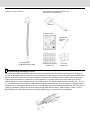
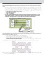
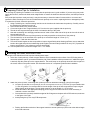
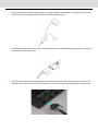
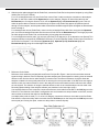
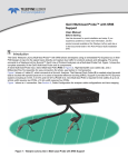
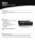
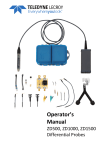
Gen3 Multi-lead Probe™ User Manual Before Starting Use this document for quick installation and setup. If you experience problems or need more information, see the product manuals available at the Teledyne LeCroy web site or in the Documents folder in the PETracer installation CD. 1 Introduction The Teledyne LeCroy Gen3 Multi-lead Probe™ is designed to tap and test inter-chip signaling on a PCI Express board. Figure 1 shows the complete assembly of the Gen3 Multi-lead Probe and its components. A Gen3 Multi-lead Probe has a Gen3 Multi-lead POD (POD in Figure 1), High Bandwidth coax cables (C), and a Differential Flex Tip Assembly for easy connection (for photo, see Section 2, Components). Figure 1 also shows a Y cable (Y), which connects to a Summit T3 Analyzer. The External Clock Cable (E) is needed only when the serial data is clocked with spread spectrum. One Multi-lead POD is required for link widths of up to x4. x8 link width requires two PODs. x16 link width requires four PODs. Figure 1 shows an x2 connection. See section 7, Cable Configuration for analyzer cable configurations and lane mapping. Y C POD E Figure 1. Teledyne LeCroy Gen3 Multi-lead Probe and Components 2 Components • High Bandwidth Coax Cable Assembly (C in Figure 1) The Teledyne LeCroy Gen3 Multi-lead Probe has the following components: • Gen3 Multi-lead POD (POD in Figure 1) • Clocking Cable Assembly • Gen3 Multi-lead Probe Differential Flex Tip • Probe Tip • Flexible Wire Probe Tip Holder • Installation Guide • Temporary (Removable) Stickers (10) • Permanent Stickers (10) Note: To connect to a Summit T3 Analyzer, you need one iPass Y cable (PE010UCA-X) for configurations up to x4, two iPass Y cables and two pods for x8 configurations, and four x4 to x8 straight iPass cables (PE013UCA-X) and four pods for x16 configurations. PE065UIA-X: G3x1 Probe Set 2ea. PE063ACA-X G3 Multi-lead Probe Tips with Probe Tip Support Bracket Probe Tip Installation Guide Flexible Wire Tip Probe Holder 2ea. PE063ACA-X G3 Multi-lead Probe Cables Temporary (Removable) Stickers (10) Permanent Stickers (10) 3 Determining Sampling Points Installing a multi-lead probe system requires some advance planning. Since the multi-lead probe system is designed for use with PCB designs that may not have been specifically laid out with probing in mind, probe points must be identified and selected to allow the system to access the embedded PCI Express bus contained within the board. Typical probe points might include exposed pins of components, coupling capacitors, or exposed traces on the board which carry the PCI Express signals. For each bi-directional lane of a PCI Express bus, four signals must be captured: The Rx+, Rx-, Tx+ and Tx- of each lane must all be sampled to capture data traffic going in each direction. So for a x1 design, four signals must be sampled; for a x2, eight signals, and so on up to a x16 design which requires 64 individual sample points.The G3 multi-lead probe tip is designed to sample two points in close proximity, either the Rx+ and Rx- differential pair, or the Tx+ and Txdifferential pair. So each bi-directional lane requires two probe tips (up to 32 probe tips for x16 designs). Once possible probe locations have been identified, the locations to be used must be selected considering the following criteria: 1. The probe locations must be within sufficient physical proximity to each other that the probe cables and probe tips can easily reach back to the probe pod, which gathers and amplifies the signals prior to passing them along to the analyzer. Each probe pod handles up to eight (8) probe tips. The probe pods are then connected back to the analyzer using 1 meter iPass cables (either Y-cables for x1, x2 and x4 designs, or straight x4-to-x8 iPass cables for x8 and x16 designs). The dimensions of the probe components are as follows: • Probe Pod: 163 x 37 x 106 mm (6.4” x1.5” x 4.2”) • Probe Cable: 294 mm (11.6”) • Probe Tip: 71 mm (2.8”) 2. The probe locations should be selected to provide the best possible signal with minimum distortion of the PCI Express channel connection. As a general rule of thumb, this location is typically just beyond the AC coupling capacitor that should be positioned as near as possible to the transmitter (see illustration below). If an oscilloscope is available to make measurements, the probe requires the following minimum signal requirements at a given bit error rate at the analyzer probe point: • Inner eye width = 82 ps Minimum (see 1 in the following figure) • Inner eye height = 52 mVpp Minimum (see 2 in the following figure) • Maximum signal amplitude 1500 mVpp Maximum (see 3 in the following figure) • If measurements/simulations are not available, the optimal location is typically at the AC coupling caps near the transmitter which offers the highest eye margins. Once probe points have been selected, you are now ready to prepare for installation of the Gen3 Multi-lead Probe. Note: As an aid in calculating the differential impedance with probes installed, the probe impedance is 600Ω typical, >400Ω at 4 GHz and >300Ω at 12 GHz. 4 Preparing Probe Tips for Installation The first step in preparing for installation is to ensure that the probe tips are in good condition. If you are using new probe tips for the first time, examine the leads under magnification to ensure the leads are clean and secure, and then proceed to step 6. If the probe tips have been used previously, it may be necessary to clean the leads of excess solder or to remove and replace the leads. Small spool of wire is included with each probe tip to be used in replacing broken or damaged tip leads. To replace the tip leads, follow this procedure: 1. Using a soldering iron, heat the existing lead wire at the via where the lead enters the probe tip. Carefully remove the existing wire segment from the via. 2. Clean the via barrel of any excess solder. 3. Cut a new length of wire of approximately 2-3” from the wire spool supplied with the probe tip. 4. Thread the wire segment through the clean via located at the tip of the probe. 5. Heat with a soldering iron and apply small amounts of solder on the under-side of the tip at the via until the wire is secured within the via. 6. Trim the excess wire on the top of the probe tip as closely as possible to the surface of the probe tip. 7. Trim the lead wire on the underside of the probe tip to a maximum length of 2.5 mm (0.1”). 8. Repeat steps 1-7 with the other lead wire. 9. Trim the final lead lengths as short as possible to improve signal fidelity while allowing sufficient room to attach the leads to the signal test point and maintaining equal lengths of the two leads [to within 0.25 mm (0.01”) if possible to improve signal fidelity—use calipers to measure lead length]. 10. Trim the probe wire to a maximum length of 0.1 0.01 inches. 5 Installing the Gen3 Multi-lead Probe Installing the Gen3 Multi-lead Probe requires following these steps: 1. At the site of each probe tip, install a support bracket, which is attached to the surface of the PCB using either a removable adhesive pad or a permanent adhesive pad (if the installation will be permanent or if additional support is desired). Slip the probe tip into the support bracket. The small bump on the probe tip head will click into place in the recess visible in the probe bracket. See illustrations below of a completed probe bracket installation. 2. Attach the probe tip leads, connecting each probe tip to the two differential sampling points for that signal. a. Use probe tip leads that are of equal length, and are not longer than 2.5 mm (0.1”).The Flex Tip is pre-installed with 0.1 inch long leads. It is recommended to trim the length of the tip as short as possible to improve signal fidelity margin at the analyzer. The two leads must be cut to the length of +/- 0.01 inches. b. Solder the leads to the appropriate sampling points using the minimum amount of solder necessary to maintain a secure connection. c. Once soldered, the probe tip should be angled at 30-45 degrees to the plane of the PCB under test, as shown in the figure to the right. d. Avoid placing the tip over any PCB components. e. Position the flexible metal wire of the support bracket to hold the probe tip in place and at the desired angle to the PCB under test. 3. Once the probe tip has been installed properly in the support bracket and soldered to the sampling points on the PCB under test, the installed probe tip should look like the illustration below. 4. Each probe tip should then be connected to the high bandwidth coax cable assembly by plugging the probe tip into the smaller end of the probe cable. 5. The probe cables should then be plugged into the probe pod(s), starting with the lowest left port as shown in the illustration at the right. See section 7 for information on how to connect the cables under different configurations. 6. With the probe cables plugged into the Probe Pod, connect the Probe Pod to the protocol analyzer by using iPass cables (see A in Figure 1 below). For x1 to x4 designs that use only one Probe Pod, use an iPass Y-cable to make the connection to the analyzer. Plug the “A” side of the cable into the Upstream port on the analyzer. Plug the “B” side of the cable into the Downstream port. If using the Summit T3-16, use the Upstream (0-7) and Downstream (0-7) ports. This will make the probe cables connected to the A0 through A3 ports on the Probe Pod appear as Upstream lanes 0 through 3 on the analyzer, and the probe cables connected to the B0 through B3 ports will appear as Downstream lanes 0 through 3. For x8 designs that use two Probe Pods, connect a x4-to-x8 straight iPass cable from one pod to the Upstream port, and a second straight iPass cable from the second Probe Pod to the Downstream port. The larger (x8) end of the cable plugs into the Probe Pod, and the smaller (x4) end plugs into the analyzer. For x16 designs that use four pods, you must use a Summit T3-16 analyzer (or, as an alternative, two Summit T3-8 analyzers which are connected by a PE060ACA-X Summit T3-8 x16 Expansion Cable). Connect one Probe Pod to each of the four Summit T3-16 connectors [Upstream (0-7), Upstream (8-15), Downstream (0-7) and Downstream (8-15)] using x4-to-x8 straight iPass cables. A B Figure 1 7. Reference Clock Cables Reference clock cables are provided with each Probe Pod (see B in Figure 1 above) to be used when external signal clocking is desired. If the PCI Express link under analysis uses spread-spectrum clocking, then the external reference clock from the device under test (DUT) must be used. The external reference clock also allows the analyzer to obtain lock more quickly when a link is returning from a low power state. If the DUT does not supply a reference clock, the internal reference clock in the analyzer can be used instead, and the reference clock cables are not required. The selection of using the external reference clock or the internal analyzer clock is made in the Recording Options dialog of the analyzer software (see checkbox in the lower right corner). If an external reference clock is required, connect the reference clock cable from the DUT to the CLK In port on the Probe Pod. The reference clock cable is configured at one end to attach to a two-pin header on the DUT, and the other end has a connector that clips into the CLK In port. In multiple probe pods are used (i.e., for x8 or x16 designs), connect the reference clock cable to the first Probe Pod and then connect the daisy chain clock cable from the CLK Out port on the first pod to the CLK In port on the second pod (and if using four pods, continue to daisy chain to connect all pods). 6 Differential Flex Tip Attaching the Tip to the Probing Point 1. The Flex Tip is pre-installed with 0.1 inch long leads. a. It is recommended to trim the length of the tip as short as possible to improve signal fidelity margin at the analyzer. The two leads must be cut to the length of +/- 0.01 inches. 2. Once soldered, the tip head must be angled at 30-45 degrees to the plane of printed circuit board. Refer to the following figure. a. Avoid placing the tip directly over any components. b. A tip holder, supplied with the probe, can be used to secure the tip assembly at the desired angle. Tip Wire Replacement Perform the following procedure to replace the tip wire: 1. Heat the wire at the via with the soldering iron. Carefully remove the existing wire segment from the via. 2. Free the via barrel of excess solder. 3. Cut approximately two to three inch wire segment from the wire spool (supplied). 4. Thread the wire segment through the via located at the tip. 5. Apply small amounts of solder on the under-side of the tip at the via and heat with a soldering iron until the wire is retained in the via. 6. Trim the wire on the top of the flex tip as short as possible to the surface of the printed circuit board. 7. Trim the probe wire to a maximum length of 0.1, 0.01 inches. 7 Cable Configuration Probe Cable Configuration for x1 to x4 Designs The x1 -x4 configuration uses 1 POD and the Y analyzer cable. Connect the Probe tips to the POD according to the following table: Probe Lane Upstream lane 0 Upstream lane 1 Upstream lane 2 Upstream lane 3 Downstream lane 0 Downstream lane 1 Downstream lane 2 Downstream lane 3 • • POD Connection A0 A1 A2 A3 B0 B1 B2 B3 Connect the A side of the Y cable to Upstream connector on the analyzer. Connect the B side of the Y cable to Downstream connector on the analyzer. Note: If using T24, only a straight cable is needed from POD to Analyzer. PCI Express designs that use x1 through x4 designs use one Gen3 Probe Pod. The probe cables are connected to the probe pod as shown in the table below: So for a x1 design, the two probe cables would be plugged into A0 and B0. For a x2 design, the four probe cables would be plugged into A0, B0, A1 and B1. For a x4 design, all eight ports on a single probe pod would be fully populated. The “A” and “B” designations refer to the routing of the signals through the iPass Y-cable which is used in PCIe designs up to x4 to connect the single probe pod to both the “Upstream” and “Downstream” ports of the analyzer. Normally the “A” cable is attached to the “Upstream” [or “Upstream (0-7)”] analyzer port, and the channels connected to the A0 through A3 ports will show up as the Upstream channels of Lanes 0-3, respectively. x8 Configuration Designs with lane widths larger that x4 require multiple probe pods, and instead of using an iPass Y-cable, x4-to-x8 straight iPass cables are used. So for a x8 design, two probe pods are required, and one carries the “Upstream” lanes 0-7 while the second carries the “Downstream” lanes 0-7. Which pod is “Upstream” and which is “Downstream” depends on which ports the iPass cables are plugged into on the analyzer. There is no difference in the actual pods themselves. Both pods are fully populated as shown in the illustration below. The x8 configuration uses 2 PODs and 2 Straight Analyzer cables. • Connect the Upstream lanes to one POD according to the Lane Mapping of the Straight Analyzer Cable (0-7). • Use the Straight Analyzer cable to connect the POD to the Upstream port on the analyzer. • Do the same for Downstream channels using the second POD. Connect to Upstream port on analyzer Connect to Downstream port on analyzer x16 Configuration The x16 configuration uses 4 PODs and 4 x4 to x8 iPass Straight Analyzer cables (PE013UCA-X). • Connect the Upstream channels 0-7 to one POD according to the Lane Mapping of the Straight Analyzer cable (0-7). • Use the Straight Analyzer cable to connect the POD to Upstream 0-7 ports on the analyzer. • Connect the Upstream channels 8-15 to another POD according to Lane Mapping of the Straight Analyzer cable (0-7). Upstream Lane 8 should be connected to lane 0 on the POD, and Upstream lane 15 should be connected to lane 7 on the POD. • Use the Straight Analyzer cable to connect the POD to Upstream 8-15 ports on the analyzer. • Do the same for Downstream channels using the other PODs. x16 PCI Express designs require four probe pods, all of which will be fully populated with 32 cables required to capture bi-directional x16 traffic. The probe pods are configured as follows: Connect to Upstream 8-15 port on analyzer Connect to Downstream 8-15 port on analyzer 8 Recording Traffic After the Summit Analyzer and Multi-Lead Probe are properly setup, use the PETracer software to record traffic in the link. Follow the instructions in the user manual that came with your analyzer to install the software on the host CPU, which can be connected to the analyzer via a USB or Ethernet connection. For instructions on setting up and implementing a recording, please refer to the PCI Express Multi-Lane Protocol Analyzer User Manual available at the Teledyne LeCroy web site or in the Documents folder in the PETracer installation CD. Teledyne LeCroy Customer Support Online Download Periodically check the Teledyne LeCroy Protocol Solutions Group web site for software updates and other support related to this product. Software updates are available to users with a current Maintenance Agreement. Mail: Web: E-mail: Tel: Tel: Fax: 3385 Scott Blvd., Santa Clara, CA 95054-3115 teledynelecroy.com/tm/Library/software/PSG [email protected] (800) 909-7112 (USA and Canada) (408) 653-1260 (worldwide) (408) 727-6622 (worldwide) Trademarks and Servicemarks Changes Teledyne LeCroy, PETracer, Summit T3-16, Summit T3-8, Summit T28 and Summit T24 are trademarks of Teledyne LeCroy, Inc. All other trademarks are property of their respective companies. Product specifications are subject to change without notice. Teledyne LeCroy reserves the right to revise the information in this document without notice or penalty. Copyright © 2013 by Teledyne LeCroy, Inc. All rights reserved. Part Number: 920672-00 Rev. A This document may be printed and reproduced without additional permission, but all copies should contain this copyright notice.