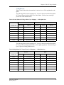
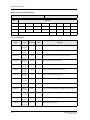
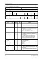
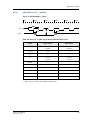
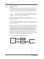
1
® QSpan II™ User Manual 8091862_MA001_08 November 2009 6024 Silver Creek Valley Road, San Jose, California 95138 Telephone: (800) 345-7015 • (408) 284-8200 • FAX: (408) 284-2775 Printed in U.S.A. ©2009 Integrated Device Technology, Inc. GENERAL DISCLAIMER Integrated Device Technology, Inc. reserves the right to make changes to its products or specifications at any time, without notice, in order to improve design or performance and to supply the best possible product. IDT does not assume any responsibility for use of any circuitry described other than the circuitry embodied in an IDT product. The Company makes no representations that circuitry described herein is free from patent infringement or other rights of third parties which may result from its use. No license is granted by implication or otherwise under any patent, patent rights or other rights, of Integrated Device Technology, Inc. CODE DISCLAIMER Code examples provided by IDT are for illustrative purposes only and should not be relied upon for developing applications. Any use of the code examples below is completely at your own risk. IDT MAKES NO REPRESENTATIONS OR WARRANTIES OF ANY KIND CONCERNING THE NONINFRINGEMENT, QUALITY, SAFETY OR SUITABILITY OF THE CODE, EITHER EXPRESS OR IMPLIED, INCLUDING WITHOUT LIMITATION ANY IMPLIED WARRANTIES OF MERCHANTABILITY, FITNESS FOR A PARTICULAR PURPOSE, OR NON-INFRINGEMENT. FURTHER, IDT MAKES NO REPRESENTATIONS OR WARRANTIES AS TO THE TRUTH, ACCURACY OR COMPLETENESS OF ANY STATEMENTS, INFORMATION OR MATERIALS CONCERNING CODE EXAMPLES CONTAINED IN ANY IDT PUBLICATION OR PUBLIC DISCLOSURE OR THAT IS CONTAINED ON ANY IDT INTERNET SITE. IN NO EVENT WILL IDT BE LIABLE FOR ANY DIRECT, CONSEQUENTIAL, INCIDENTAL, INDIRECT, PUNITIVE OR SPECIAL DAMAGES, HOWEVER THEY MAY ARISE, AND EVEN IF IDT HAS BEEN PREVIOUSLY ADVISED ABOUT THE POSSIBILITY OF SUCH DAMAGES. The code examples also may be subject to United States export control laws and may be subject to the export or import laws of other countries and it is your responsibility to comply with any applicable laws or regulations. LIFE SUPPORT POLICY Integrated Device Technology's products are not authorized for use as critical components in life support devices or systems unless a specific written agreement pertaining to such intended use is executed between the manufacturer and an officer of IDT. 1. Life support devices or systems are devices or systems which (a) are intended for surgical implant into the body or (b) support or sustain life and whose failure to perform, when properly used in accordance with instructions for use provided in the labeling, can be reasonably expected to result in a significant injury to the user. 2. A critical component is any components of a life support device or system whose failure to perform can be reasonably expected to cause the failure of the life support device or system, or to affect its safety or effectiveness. IDT, the IDT logo, and Integrated Device Technology are trademarks or registered trademarks of Integrated Device Technology, Inc. Revision History 8091862.MA001.08, Final Manual, November 2009 This version of the document was rebranded as IDT. It does not include any technical changes. 8091862.MA001.07, Final Manual, January 2007 • Corrected the description of the BS field in the PBTI0_CTL, PBTI1_CTL, QBSI0_AT, and QBSI1_AT registers (see “Register Map” on page 197). • Updated the Ordering Information section to indicate a reduction in the variety of QSpan II parts available to customers (see “Ordering Information” on page 407). 8091862.MA001.06, Final Manual, September 2000 8091862.MA001.05, Final Manual, September 2000 8091862.MA001.04, Preliminary Manual, December 1999 8091862.MA001.03, Preliminary Manual, September 1999 8091862.MA001.02, Preliminary Manual, September 1999 8091862.MA001.01, Preliminary Manual, August 1999 QSpan II User Manual 8091862_MA001_08 3 Revision History 4 QSpan II User Manual 8091862_MA001_08 Contents Chapter 1: General Information . . . . . . . . . . . . . . . . . . . . . . . . . . . . . . . . . . . . . . . 25 1.1 1.2 1.3 What is the QSpan II . . . . . . . . . . . . . . . . . . . . . . . . . . . . . . . . . . . . . . . . . . . . . . . . . . . . . . . . . 26 1.1.1 QSpan II Features . . . . . . . . . . . . . . . . . . . . . . . . . . . . . . . . . . . . . . . . . . . . . . . . . . . . . 27 1.1.2 QSpan II verses QSpan. . . . . . . . . . . . . . . . . . . . . . . . . . . . . . . . . . . . . . . . . . . . . . . . . 28 Document Conventions . . . . . . . . . . . . . . . . . . . . . . . . . . . . . . . . . . . . . . . . . . . . . . . . . . . . . . . 29 1.2.1 Signals . . . . . . . . . . . . . . . . . . . . . . . . . . . . . . . . . . . . . . . . . . . . . . . . . . . . . . . . . . . . . 29 1.2.2 Bit Ordering . . . . . . . . . . . . . . . . . . . . . . . . . . . . . . . . . . . . . . . . . . . . . . . . . . . . . . . . . 29 1.2.3 Numeric Conventions. . . . . . . . . . . . . . . . . . . . . . . . . . . . . . . . . . . . . . . . . . . . . . . . . . 29 1.2.4 Topographic Conventions . . . . . . . . . . . . . . . . . . . . . . . . . . . . . . . . . . . . . . . . . . . . . . 29 1.2.5 Symbols . . . . . . . . . . . . . . . . . . . . . . . . . . . . . . . . . . . . . . . . . . . . . . . . . . . . . . . . . . . . 30 1.2.6 Document Status. . . . . . . . . . . . . . . . . . . . . . . . . . . . . . . . . . . . . . . . . . . . . . . . . . . . . . 30 Related Documentation . . . . . . . . . . . . . . . . . . . . . . . . . . . . . . . . . . . . . . . . . . . . . . . . . . . . . . . 30 Chapter 2: Functional Overview . . . . . . . . . . . . . . . . . . . . . . . . . . . . . . . . . . . . . . . 31 2.1 Overview . . . . . . . . . . . . . . . . . . . . . . . . . . . . . . . . . . . . . . . . . . . . . . . . . . . . . . . . . . . . . . . . . . 31 2.2 The QBus Slave Channel . . . . . . . . . . . . . . . . . . . . . . . . . . . . . . . . . . . . . . . . . . . . . . . . . . . . . 32 2.3 The PCI Target Channel . . . . . . . . . . . . . . . . . . . . . . . . . . . . . . . . . . . . . . . . . . . . . . . . . . . . . . 33 2.4 The IDMA Channel. . . . . . . . . . . . . . . . . . . . . . . . . . . . . . . . . . . . . . . . . . . . . . . . . . . . . . . . . . 33 2.5 The DMA Channel . . . . . . . . . . . . . . . . . . . . . . . . . . . . . . . . . . . . . . . . . . . . . . . . . . . . . . . . . . 33 2.6 The Register Channel . . . . . . . . . . . . . . . . . . . . . . . . . . . . . . . . . . . . . . . . . . . . . . . . . . . . . . . . 33 2.7 The Interrupt Channel . . . . . . . . . . . . . . . . . . . . . . . . . . . . . . . . . . . . . . . . . . . . . . . . . . . . . . . . 34 2.8 The EEPROM Channel . . . . . . . . . . . . . . . . . . . . . . . . . . . . . . . . . . . . . . . . . . . . . . . . . . . . . . . 34 Chapter 3: The QBus Slave Channel . . . . . . . . . . . . . . . . . . . . . . . . . . . . . . . . . . . 35 3.1 Overview . . . . . . . . . . . . . . . . . . . . . . . . . . . . . . . . . . . . . . . . . . . . . . . . . . . . . . . . . . . . . . . . . . 35 3.2 QBus Slave Channel Architecture . . . . . . . . . . . . . . . . . . . . . . . . . . . . . . . . . . . . . . . . . . . . . . 36 3.2.1 QBus Slave Module . . . . . . . . . . . . . . . . . . . . . . . . . . . . . . . . . . . . . . . . . . . . . . . . . . . 37 QSpan II User Manual 8091862_MA001_08 5 Contents 3.2.1.1 QBus Data Parity Generation and Detection . . . . . . . . . . . . . . . . . . . . . . . . . 37 3.2.2 Qx-FIFO and Qr-FIFO . . . . . . . . . . . . . . . . . . . . . . . . . . . . . . . . . . . . . . . . . . . . . . . . . 38 3.2.3 PCI Master Module. . . . . . . . . . . . . . . . . . . . . . . . . . . . . . . . . . . . . . . . . . . . . . . . . . . . 38 3.3 Channel Description . . . . . . . . . . . . . . . . . . . . . . . . . . . . . . . . . . . . . . . . . . . . . . . . . . . . . . . . . 38 3.4 Address Phase . . . . . . . . . . . . . . . . . . . . . . . . . . . . . . . . . . . . . . . . . . . . . . . . . . . . . . . . . . . . . . 39 3.4.1 Transaction Decoding and QBus Slave Images . . . . . . . . . . . . . . . . . . . . . . . . . . . . . . 39 3.4.1.1 MPC860 Cycles . . . . . . . . . . . . . . . . . . . . . . . . . . . . . . . . . . . . . . . . . . . . . . . 41 3.4.1.2 MC68360 Cycles . . . . . . . . . . . . . . . . . . . . . . . . . . . . . . . . . . . . . . . . . . . . . . 41 3.4.1.3 M68040 Cycles. . . . . . . . . . . . . . . . . . . . . . . . . . . . . . . . . . . . . . . . . . . . . . . . 41 3.5 3.4.2 PCI Bus Request . . . . . . . . . . . . . . . . . . . . . . . . . . . . . . . . . . . . . . . . . . . . . . . . . . . . . . 42 3.4.3 Address Translation . . . . . . . . . . . . . . . . . . . . . . . . . . . . . . . . . . . . . . . . . . . . . . . . . . . 42 3.4.4 Address Phase on the PCI Bus . . . . . . . . . . . . . . . . . . . . . . . . . . . . . . . . . . . . . . . . . . . 45 Data Phase . . . . . . . . . . . . . . . . . . . . . . . . . . . . . . . . . . . . . . . . . . . . . . . . . . . . . . . . . . . . . . . . . 46 3.5.1 Endian Mapping . . . . . . . . . . . . . . . . . . . . . . . . . . . . . . . . . . . . . . . . . . . . . . . . . . . . . . 46 3.5.2 Data Path . . . . . . . . . . . . . . . . . . . . . . . . . . . . . . . . . . . . . . . . . . . . . . . . . . . . . . . . . . . . 48 3.5.2.1 Writes . . . . . . . . . . . . . . . . . . . . . . . . . . . . . . . . . . . . . . . . . . . . . . . . . . . . . . . 48 3.5.2.2 Read Transactions — Burst and Single Cycle . . . . . . . . . . . . . . . . . . . . . . . . 50 3.5.2.3 Prefetched Reads . . . . . . . . . . . . . . . . . . . . . . . . . . . . . . . . . . . . . . . . . . . . . . 50 3.5.2.4 Delayed Reads and PCI Transaction Ordering. . . . . . . . . . . . . . . . . . . . . . . . 51 3.6 3.5.3 PCI Target Channel Reads . . . . . . . . . . . . . . . . . . . . . . . . . . . . . . . . . . . . . . . . . . . . . . 52 3.5.4 Parity Monitoring by PCI Master Module . . . . . . . . . . . . . . . . . . . . . . . . . . . . . . . . . . 52 Termination Phase . . . . . . . . . . . . . . . . . . . . . . . . . . . . . . . . . . . . . . . . . . . . . . . . . . . . . . . . . . . 53 3.6.1 3.7 Posted Write Termination . . . . . . . . . . . . . . . . . . . . . . . . . . . . . . . . . . . . . . . . . . . . . . . 55 PCI Master Retry Counter . . . . . . . . . . . . . . . . . . . . . . . . . . . . . . . . . . . . . . . . . . . . . . . . . . . . . 56 Chapter 4: The PCI Target Channel . . . . . . . . . . . . . . . . . . . . . . . . . . . . . . . . . . . 57 4.1 Overview . . . . . . . . . . . . . . . . . . . . . . . . . . . . . . . . . . . . . . . . . . . . . . . . . . . . . . . . . . . . . . . . . . 57 4.2 PCI Target Channel Architecture . . . . . . . . . . . . . . . . . . . . . . . . . . . . . . . . . . . . . . . . . . . . . . . 58 4.2.1 PCI Target Module . . . . . . . . . . . . . . . . . . . . . . . . . . . . . . . . . . . . . . . . . . . . . . . . . . . . 58 4.2.2 Px-FIFO and Pr-FIFO . . . . . . . . . . . . . . . . . . . . . . . . . . . . . . . . . . . . . . . . . . . . . . . . . . 59 4.2.3 QBus Master Module . . . . . . . . . . . . . . . . . . . . . . . . . . . . . . . . . . . . . . . . . . . . . . . . . . 59 4.2.3.1 QBus Data Parity Generation and Detection . . . . . . . . . . . . . . . . . . . . . . . . . 60 4.3 Channel Description . . . . . . . . . . . . . . . . . . . . . . . . . . . . . . . . . . . . . . . . . . . . . . . . . . . . . . . . . 60 4.4 Address Phase . . . . . . . . . . . . . . . . . . . . . . . . . . . . . . . . . . . . . . . . . . . . . . . . . . . . . . . . . . . . . . 61 4.4.1 6 Transaction Decoding . . . . . . . . . . . . . . . . . . . . . . . . . . . . . . . . . . . . . . . . . . . . . . . . . . 61 QSpan II User Manual 8091862_MA001_08 Contents 4.4.2 Address Translation . . . . . . . . . . . . . . . . . . . . . . . . . . . . . . . . . . . . . . . . . . . . . . . . . . . 64 4.4.3 Transaction Codes on the QBus . . . . . . . . . . . . . . . . . . . . . . . . . . . . . . . . . . . . . . . . . . 66 4.4.4 PCI BIOS Memory Allocation . . . . . . . . . . . . . . . . . . . . . . . . . . . . . . . . . . . . . . . . . . . 67 4.4.4.1 Block Size and PCI Address Space . . . . . . . . . . . . . . . . . . . . . . . . . . . . . . . . 67 4.4.4.2 Base Address . . . . . . . . . . . . . . . . . . . . . . . . . . . . . . . . . . . . . . . . . . . . . . . . . 67 4.5 Data Phase . . . . . . . . . . . . . . . . . . . . . . . . . . . . . . . . . . . . . . . . . . . . . . . . . . . . . . . . . . . . . . . . . 68 4.5.1 Endian Mapping . . . . . . . . . . . . . . . . . . . . . . . . . . . . . . . . . . . . . . . . . . . . . . . . . . . . . . 68 4.5.1.1 Write Cycle Mapping for PCI Target Channel . . . . . . . . . . . . . . . . . . . . . . . 68 4.5.1.2 Read Cycle Mapping for PCI Target Channel. . . . . . . . . . . . . . . . . . . . . . . . 70 4.5.2 Data Path . . . . . . . . . . . . . . . . . . . . . . . . . . . . . . . . . . . . . . . . . . . . . . . . . . . . . . . . . . . 74 4.5.2.1 Posted Writes . . . . . . . . . . . . . . . . . . . . . . . . . . . . . . . . . . . . . . . . . . . . . . . . . 74 4.5.2.2 Delayed Writes. . . . . . . . . . . . . . . . . . . . . . . . . . . . . . . . . . . . . . . . . . . . . . . . 75 4.5.2.3 Single Read Transactions. . . . . . . . . . . . . . . . . . . . . . . . . . . . . . . . . . . . . . . . 76 4.5.2.4 Prefetched Read Transactions . . . . . . . . . . . . . . . . . . . . . . . . . . . . . . . . . . . . 76 4.5.3 4.6 Reads and PCI Transaction Ordering . . . . . . . . . . . . . . . . . . . . . . . . . . . . . . . . . . . . . . . . . . . . 77 4.6.1 4.7 4.8 Parity Monitoring by PCI Target Module . . . . . . . . . . . . . . . . . . . . . . . . . . . . . . . . . . 77 Transaction Ordering Disable Option . . . . . . . . . . . . . . . . . . . . . . . . . . . . . . . . . . . . . 78 QBus Arbitration and Sampling . . . . . . . . . . . . . . . . . . . . . . . . . . . . . . . . . . . . . . . . . . . . . . . . 78 4.7.1 MC68360 Bus Arbitration . . . . . . . . . . . . . . . . . . . . . . . . . . . . . . . . . . . . . . . . . . . . . . 78 4.7.2 MPC860 Bus Arbitration . . . . . . . . . . . . . . . . . . . . . . . . . . . . . . . . . . . . . . . . . . . . . . . 79 4.7.3 M68040 Bus Arbitration. . . . . . . . . . . . . . . . . . . . . . . . . . . . . . . . . . . . . . . . . . . . . . . . 80 Terminations . . . . . . . . . . . . . . . . . . . . . . . . . . . . . . . . . . . . . . . . . . . . . . . . . . . . . . . . . . . . . . . 80 4.8.1 QBus Master Module Terminations . . . . . . . . . . . . . . . . . . . . . . . . . . . . . . . . . . . . . . . 80 4.8.2 MC68360 Cycle Terminations . . . . . . . . . . . . . . . . . . . . . . . . . . . . . . . . . . . . . . . . . . . 80 4.8.3 MPC860 Cycle Terminations . . . . . . . . . . . . . . . . . . . . . . . . . . . . . . . . . . . . . . . . . . . . 81 4.8.4 M68040 Cycle Terminations . . . . . . . . . . . . . . . . . . . . . . . . . . . . . . . . . . . . . . . . . . . . 81 4.8.5 Terminations driven by the PCI Target Module. . . . . . . . . . . . . . . . . . . . . . . . . . . . . . 82 4.8.5.1 Target-Disconnect . . . . . . . . . . . . . . . . . . . . . . . . . . . . . . . . . . . . . . . . . . . . . 82 4.8.5.2 Target-Retry. . . . . . . . . . . . . . . . . . . . . . . . . . . . . . . . . . . . . . . . . . . . . . . . . . 83 4.8.5.3 Target-Abort . . . . . . . . . . . . . . . . . . . . . . . . . . . . . . . . . . . . . . . . . . . . . . . . . 83 4.8.6 Terminations of Posted Writes . . . . . . . . . . . . . . . . . . . . . . . . . . . . . . . . . . . . . . . . . . . 84 Chapter 5: The IDMA Channel . . . . . . . . . . . . . . . . . . . . . . . . . . . . . . . . . . . . . . . . 85 5.1 Overview . . . . . . . . . . . . . . . . . . . . . . . . . . . . . . . . . . . . . . . . . . . . . . . . . . . . . . . . . . . . . . . . . . 85 5.2 PCI Read Transactions . . . . . . . . . . . . . . . . . . . . . . . . . . . . . . . . . . . . . . . . . . . . . . . . . . . . . . . 87 QSpan II User Manual 8091862_MA001_08 7 Contents 5.2.1 5.3 Data Path . . . . . . . . . . . . . . . . . . . . . . . . . . . . . . . . . . . . . . . . . . . . . . . . . . . . . . . . . . . . 88 PCI Write Transactions . . . . . . . . . . . . . . . . . . . . . . . . . . . . . . . . . . . . . . . . . . . . . . . . . . . . . . . 89 5.3.1 Data Path . . . . . . . . . . . . . . . . . . . . . . . . . . . . . . . . . . . . . . . . . . . . . . . . . . . . . . . . . . . . 89 5.4 TC[3:0] Encoding with MPC860 IDMA . . . . . . . . . . . . . . . . . . . . . . . . . . . . . . . . . . . . . . . . . . 90 5.5 IDMA Status Tracking . . . . . . . . . . . . . . . . . . . . . . . . . . . . . . . . . . . . . . . . . . . . . . . . . . . . . . . 91 5.6 IDMA Errors, Resets, and Interrupts . . . . . . . . . . . . . . . . . . . . . . . . . . . . . . . . . . . . . . . . . . . . . 91 5.7 IDMA Endian Issues . . . . . . . . . . . . . . . . . . . . . . . . . . . . . . . . . . . . . . . . . . . . . . . . . . . . . . . . . 93 Chapter 6: The DMA Channel . . . . . . . . . . . . . . . . . . . . . . . . . . . . . . . . . . . . . . . . 95 6.1 Overview . . . . . . . . . . . . . . . . . . . . . . . . . . . . . . . . . . . . . . . . . . . . . . . . . . . . . . . . . . . . . . . . . . 95 6.2 DMA Registers . . . . . . . . . . . . . . . . . . . . . . . . . . . . . . . . . . . . . . . . . . . . . . . . . . . . . . . . . . . . . 97 6.3 6.4 6.2.1 Burst Cycles . . . . . . . . . . . . . . . . . . . . . . . . . . . . . . . . . . . . . . . . . . . . . . . . . . . . . . . . . 98 6.2.2 DMA Cycles on QBus . . . . . . . . . . . . . . . . . . . . . . . . . . . . . . . . . . . . . . . . . . . . . . . . . 99 Direct Mode DMA Operation . . . . . . . . . . . . . . . . . . . . . . . . . . . . . . . . . . . . . . . . . . . . . . . . . . 99 6.3.1 Initiating a Direct Mode Transfer . . . . . . . . . . . . . . . . . . . . . . . . . . . . . . . . . . . . . . . . . 99 6.3.2 Terminating a Direct Mode Transfer . . . . . . . . . . . . . . . . . . . . . . . . . . . . . . . . . . . . . 100 Linked List Mode DMA Operation . . . . . . . . . . . . . . . . . . . . . . . . . . . . . . . . . . . . . . . . . . . . . 100 6.4.1 Initiating a Linked List Mode DMA Operation . . . . . . . . . . . . . . . . . . . . . . . . . . . . . 102 6.4.2 Terminating a Linked List Mode DMA Operation. . . . . . . . . . . . . . . . . . . . . . . . . . . 104 Chapter 7: The Register Channel . . . . . . . . . . . . . . . . . . . . . . . . . . . . . . . . . . . . . 105 7.1 Overview . . . . . . . . . . . . . . . . . . . . . . . . . . . . . . . . . . . . . . . . . . . . . . . . . . . . . . . . . . . . . . . . . 105 7.2 Register Access Fairness . . . . . . . . . . . . . . . . . . . . . . . . . . . . . . . . . . . . . . . . . . . . . . . . . . . . . 106 7.3 Register Access from the PCI Bus. . . . . . . . . . . . . . . . . . . . . . . . . . . . . . . . . . . . . . . . . . . . . . 107 7.4 Register Access from the QBus . . . . . . . . . . . . . . . . . . . . . . . . . . . . . . . . . . . . . . . . . . . . . . . . 109 7.4.1 Examples of QBus Register Accesses . . . . . . . . . . . . . . . . . . . . . . . . . . . . . . . . . . . . 110 7.4.2 PCI Configuration Cycles Generated from the QBus. . . . . . . . . . . . . . . . . . . . . . . . . 110 7.4.3 Address Phase of PCI Configuration Cycles . . . . . . . . . . . . . . . . . . . . . . . . . . . . . . . 111 7.4.3.1 Data Phase of PCI Configuration Cycles . . . . . . . . . . . . . . . . . . . . . . . . . . . 112 7.4.4 Interrupt Acknowledge Cycle . . . . . . . . . . . . . . . . . . . . . . . . . . . . . . . . . . . . . . . . . . . 112 7.5 Register Access Synchronization . . . . . . . . . . . . . . . . . . . . . . . . . . . . . . . . . . . . . . . . . . . . . . 113 7.6 Mailbox Registers . . . . . . . . . . . . . . . . . . . . . . . . . . . . . . . . . . . . . . . . . . . . . . . . . . . . . . . . . . 114 Chapter 8: The Interrupt Channel . . . . . . . . . . . . . . . . . . . . . . . . . . . . . . . . . . . . 115 8.1 Overview . . . . . . . . . . . . . . . . . . . . . . . . . . . . . . . . . . . . . . . . . . . . . . . . . . . . . . . . . . . . . . . . . 115 8.2 Hardware-Triggered Interrupts . . . . . . . . . . . . . . . . . . . . . . . . . . . . . . . . . . . . . . . . . . . . . . . . 116 8 QSpan II User Manual 8091862_MA001_08 Contents 8.3 Software-Triggered Interrupts. . . . . . . . . . . . . . . . . . . . . . . . . . . . . . . . . . . . . . . . . . . . . . . . . 117 8.3.1 Interrupt Generation due to PCI Configuration Register Status Bits . . . . . . . . . . . . . 120 8.4 Interrupt Acknowledge Cycle . . . . . . . . . . . . . . . . . . . . . . . . . . . . . . . . . . . . . . . . . . . . . . . . . 121 8.5 Disabling PCI Interrupts . . . . . . . . . . . . . . . . . . . . . . . . . . . . . . . . . . . . . . . . . . . . . . . . . . . . . 121 Chapter 9: The EEPROM Channel. . . . . . . . . . . . . . . . . . . . . . . . . . . . . . . . . . . . 123 9.1 Overview . . . . . . . . . . . . . . . . . . . . . . . . . . . . . . . . . . . . . . . . . . . . . . . . . . . . . . . . . . . . . . . . . 123 9.2 EEPROM Configuration and Plug and Play Compatibility . . . . . . . . . . . . . . . . . . . . . . . . . . 125 9.3 EEPROM I2C Protocol . . . . . . . . . . . . . . . . . . . . . . . . . . . . . . . . . . . . . . . . . . . . . . . . . . . . . . 125 9.4 Mapping of EEPROM Bits to QSpan II Registers . . . . . . . . . . . . . . . . . . . . . . . . . . . . . . . . . 126 9.5 Programming the EEPROM from the QBus or PCI Bus . . . . . . . . . . . . . . . . . . . . . . . . . . . . 129 9.5.1 Writing to the EEPROM . . . . . . . . . . . . . . . . . . . . . . . . . . . . . . . . . . . . . . . . . . . . . . 129 9.5.2 Reading from the EEPROM. . . . . . . . . . . . . . . . . . . . . . . . . . . . . . . . . . . . . . . . . . . . 130 9.6 EEPROM Access . . . . . . . . . . . . . . . . . . . . . . . . . . . . . . . . . . . . . . . . . . . . . . . . . . . . . . . . . . 130 9.7 Vital Product Data Support . . . . . . . . . . . . . . . . . . . . . . . . . . . . . . . . . . . . . . . . . . . . . . . . . . . 130 9.7.1 Reading VPD Data . . . . . . . . . . . . . . . . . . . . . . . . . . . . . . . . . . . . . . . . . . . . . . . . . . . 131 9.7.2 Writing VPD Data . . . . . . . . . . . . . . . . . . . . . . . . . . . . . . . . . . . . . . . . . . . . . . . . . . . 131 Chapter 10: I2O Messaging Unit . . . . . . . . . . . . . . . . . . . . . . . . . . . . . . . . . . . . . . 133 10.1 Overview . . . . . . . . . . . . . . . . . . . . . . . . . . . . . . . . . . . . . . . . . . . . . . . . . . . . . . . . . . . . . . . . . 133 10.2 Inbound Messaging . . . . . . . . . . . . . . . . . . . . . . . . . . . . . . . . . . . . . . . . . . . . . . . . . . . . . . . . . 134 10.3 Outbound Messaging . . . . . . . . . . . . . . . . . . . . . . . . . . . . . . . . . . . . . . . . . . . . . . . . . . . . . . . 135 10.4 I2O Operation . . . . . . . . . . . . . . . . . . . . . . . . . . . . . . . . . . . . . . . . . . . . . . . . . . . . . . . . . . . . . 136 10.5 Summary of I2O Operations . . . . . . . . . . . . . . . . . . . . . . . . . . . . . . . . . . . . . . . . . . . . . . . . . . 136 10.5.1 Initialization . . . . . . . . . . . . . . . . . . . . . . . . . . . . . . . . . . . . . . . . . . . . . . . . . . . . . . . . 136 10.5.1.1 Inbound I2O Message . . . . . . . . . . . . . . . . . . . . . . . . . . . . . . . . . . . . . . . . . 138 10.5.1.2 I2O Outbound Message . . . . . . . . . . . . . . . . . . . . . . . . . . . . . . . . . . . . . . . . 138 10.6 I2O Interrupts . . . . . . . . . . . . . . . . . . . . . . . . . . . . . . . . . . . . . . . . . . . . . . . . . . . . . . . . . . . . . 139 Chapter 11: PCI Bus Arbiter . . . . . . . . . . . . . . . . . . . . . . . . . . . . . . . . . . . . . . . . . 141 11.1 Overview . . . . . . . . . . . . . . . . . . . . . . . . . . . . . . . . . . . . . . . . . . . . . . . . . . . . . . . . . . . . . . . . . 141 11.2 Arbitration Scheme . . . . . . . . . . . . . . . . . . . . . . . . . . . . . . . . . . . . . . . . . . . . . . . . . . . . . . . . . 142 11.3 Bus Parking . . . . . . . . . . . . . . . . . . . . . . . . . . . . . . . . . . . . . . . . . . . . . . . . . . . . . . . . . . . . . . . 144 Chapter 12: CompactPCI Hot Swap Friendly Support . . . . . . . . . . . . . . . . . . . 145 12.1 Overview . . . . . . . . . . . . . . . . . . . . . . . . . . . . . . . . . . . . . . . . . . . . . . . . . . . . . . . . . . . . . . . . . 145 QSpan II User Manual 8091862_MA001_08 9 Contents 12.2 Hot Swapping with the QSpan II. . . . . . . . . . . . . . . . . . . . . . . . . . . . . . . . . . . . . . . . . . . . . . . 146 12.3 CompactPCI Hot Swap Card Insertion . . . . . . . . . . . . . . . . . . . . . . . . . . . . . . . . . . . . . . . . . . 147 12.4 CompactPCI Hot Swap Card Extraction . . . . . . . . . . . . . . . . . . . . . . . . . . . . . . . . . . . . . . . . . 149 Chapter 13: PCI Power Management Event Support. . . . . . . . . . . . . . . . . . . . . 153 13.1 Overview . . . . . . . . . . . . . . . . . . . . . . . . . . . . . . . . . . . . . . . . . . . . . . . . . . . . . . . . . . . . . . . . . 153 13.2 Power Management Event (PME#) Support . . . . . . . . . . . . . . . . . . . . . . . . . . . . . . . . . . . . . . 153 Chapter 14: Reset Options. . . . . . . . . . . . . . . . . . . . . . . . . . . . . . . . . . . . . . . . . . . 155 14.1 Types of Resets . . . . . . . . . . . . . . . . . . . . . . . . . . . . . . . . . . . . . . . . . . . . . . . . . . . . . . . . . . . . 155 14.1.1 PCI Transactions during QBus Reset . . . . . . . . . . . . . . . . . . . . . . . . . . . . . . . . . . . . . 156 14.1.2 IDMA Reset . . . . . . . . . . . . . . . . . . . . . . . . . . . . . . . . . . . . . . . . . . . . . . . . . . . . . . . . 156 14.1.3 Clocking and Resets . . . . . . . . . . . . . . . . . . . . . . . . . . . . . . . . . . . . . . . . . . . . . . . . . . 156 14.2 Configuration Options at Reset . . . . . . . . . . . . . . . . . . . . . . . . . . . . . . . . . . . . . . . . . . . . . . . . 157 14.2.1 PCI Bus Master Reset Option . . . . . . . . . . . . . . . . . . . . . . . . . . . . . . . . . . . . . . . . . . . 157 14.2.2 QBus Master and Slave Modes. . . . . . . . . . . . . . . . . . . . . . . . . . . . . . . . . . . . . . . . . . 158 14.2.3 EEPROM Loading . . . . . . . . . . . . . . . . . . . . . . . . . . . . . . . . . . . . . . . . . . . . . . . . . . . 158 14.2.4 PCI Register Access Option . . . . . . . . . . . . . . . . . . . . . . . . . . . . . . . . . . . . . . . . . . . . 158 14.2.5 PCI Bus Arbitration Option . . . . . . . . . . . . . . . . . . . . . . . . . . . . . . . . . . . . . . . . . . . . 158 Chapter 15: Hardware Implementation Issues . . . . . . . . . . . . . . . . . . . . . . . . . . 159 15.1 Test Mode Pins . . . . . . . . . . . . . . . . . . . . . . . . . . . . . . . . . . . . . . . . . . . . . . . . . . . . . . . . . . . . 159 15.2 JTAG Support . . . . . . . . . . . . . . . . . . . . . . . . . . . . . . . . . . . . . . . . . . . . . . . . . . . . . . . . . . . . . 160 15.3 Decoupling Capacitors. . . . . . . . . . . . . . . . . . . . . . . . . . . . . . . . . . . . . . . . . . . . . . . . . . . . . . . 160 Chapter 16: Signals. . . . . . . . . . . . . . . . . . . . . . . . . . . . . . . . . . . . . . . . . . . . . . . . . 161 16.1 Terminology . . . . . . . . . . . . . . . . . . . . . . . . . . . . . . . . . . . . . . . . . . . . . . . . . . . . . . . . . . . . . . 161 16.2 Overview . . . . . . . . . . . . . . . . . . . . . . . . . . . . . . . . . . . . . . . . . . . . . . . . . . . . . . . . . . . . . . . . . 162 16.3 MC68360 Signals: QUICC . . . . . . . . . . . . . . . . . . . . . . . . . . . . . . . . . . . . . . . . . . . . . . . . . . . 163 16.4 MPC860 Signals: PowerQUICC . . . . . . . . . . . . . . . . . . . . . . . . . . . . . . . . . . . . . . . . . . . . . . 167 16.5 M68040 Signals . . . . . . . . . . . . . . . . . . . . . . . . . . . . . . . . . . . . . . . . . . . . . . . . . . . . . . . . . . . . 171 16.6 PCI Bus Signals . . . . . . . . . . . . . . . . . . . . . . . . . . . . . . . . . . . . . . . . . . . . . . . . . . . . . . . . . . . . 174 16.7 Hot Swap Signals. . . . . . . . . . . . . . . . . . . . . . . . . . . . . . . . . . . . . . . . . . . . . . . . . . . . . . . . . . . 176 16.8 Miscellaneous Signals . . . . . . . . . . . . . . . . . . . . . . . . . . . . . . . . . . . . . . . . . . . . . . . . . . . . . . . 177 16.9 JTAG Signals. . . . . . . . . . . . . . . . . . . . . . . . . . . . . . . . . . . . . . . . . . . . . . . . . . . . . . . . . . . . . . 178 10 QSpan II User Manual 8091862_MA001_08 Contents Chapter 17: Signals and DC Characteristics . . . . . . . . . . . . . . . . . . . . . . . . . . . . 179 17.1 Terminology . . . . . . . . . . . . . . . . . . . . . . . . . . . . . . . . . . . . . . . . . . . . . . . . . . . . . . . . . . . . . . 179 17.2 Packaging and Voltage Level Support . . . . . . . . . . . . . . . . . . . . . . . . . . . . . . . . . . . . . . . . . . 180 17.3 Signals and DC Characteristics . . . . . . . . . . . . . . . . . . . . . . . . . . . . . . . . . . . . . . . . . . . 180 17.4 Pinout . . . . . . . . . . . . . . . . . . . . . . . . . . . . . . . . . . . . . . . . . . . . . . . . . . . . . . . . . . . . . . . . . . . 192 Appendix A: Registers . . . . . . . . . . . . . . . . . . . . . . . . . . . . . . . . . . . . . . . . . . . . . . 195 A.1 Overview . . . . . . . . . . . . . . . . . . . . . . . . . . . . . . . . . . . . . . . . . . . . . . . . . . . . . . . . . . . . . . . . . 195 A.2 Terminology . . . . . . . . . . . . . . . . . . . . . . . . . . . . . . . . . . . . . . . . . . . . . . . . . . . . . . . . . . . . . . 196 A.3 Register Map . . . . . . . . . . . . . . . . . . . . . . . . . . . . . . . . . . . . . . . . . . . . . . . . . . . . . . . . . . . . . 197 A.4 Registers . . . . . . . . . . . . . . . . . . . . . . . . . . . . . . . . . . . . . . . . . . . . . . . . . . . . . . . . . . . . . . . . . 202 Appendix B: Timing . . . . . . . . . . . . . . . . . . . . . . . . . . . . . . . . . . . . . . . . . . . . . . . . 301 B.1 Overview . . . . . . . . . . . . . . . . . . . . . . . . . . . . . . . . . . . . . . . . . . . . . . . . . . . . . . . . . . . . . . . . . 301 B.2 Timing Parameters . . . . . . . . . . . . . . . . . . . . . . . . . . . . . . . . . . . . . . . . . . . . . . . . . . . . . . . . . 302 B.3 Wait State Insertion — QBus Slave Module . . . . . . . . . . . . . . . . . . . . . . . . . . . . . . . . . . . . . 316 B.4 Timing Diagrams . . . . . . . . . . . . . . . . . . . . . . . . . . . . . . . . . . . . . . . . . . . . . . . . . . . . . . . . . . 317 B.4.1 QBus Interface — MC68360 . . . . . . . . . . . . . . . . . . . . . . . . . . . . . . . . . . . . . . . . . . . 317 B.4.2 QBus Master Cycles — MC68360. . . . . . . . . . . . . . . . . . . . . . . . . . . . . . . . . . . . . . . 317 B.4.2.1 QBus Slave Cycles — MC68360 . . . . . . . . . . . . . . . . . . . . . . . . . . . . . . . . 320 B.4.2.2 QBus IDMA Cycles — MC68360. . . . . . . . . . . . . . . . . . . . . . . . . . . . . . . . 324 B.4.3 QBus Interface — MPC860 . . . . . . . . . . . . . . . . . . . . . . . . . . . . . . . . . . . . . . . . . . . . 332 B.4.3.1 QBus Master Cycles — MPC860 . . . . . . . . . . . . . . . . . . . . . . . . . . . . . . . . 332 B.4.3.2 QBus Slave Cycle — MPC860 . . . . . . . . . . . . . . . . . . . . . . . . . . . . . . . . . . 337 B.4.3.3 QBus IDMA Cycles — MPC860 . . . . . . . . . . . . . . . . . . . . . . . . . . . . . . . . 343 B.4.4 QBus Interface — M68040 . . . . . . . . . . . . . . . . . . . . . . . . . . . . . . . . . . . . . . . . . . . . 347 B.4.4.1 QBus Master Cycles — M68040. . . . . . . . . . . . . . . . . . . . . . . . . . . . . . . . . 348 B.4.4.2 QBus Slave Cycles — M68040 . . . . . . . . . . . . . . . . . . . . . . . . . . . . . . . . . . 351 B.4.5 Interrupts and Resets . . . . . . . . . . . . . . . . . . . . . . . . . . . . . . . . . . . . . . . . . . . . . . . . . 357 B.4.6 Reset Options . . . . . . . . . . . . . . . . . . . . . . . . . . . . . . . . . . . . . . . . . . . . . . . . . . . . . . . 359 Appendix C: Typical Applications . . . . . . . . . . . . . . . . . . . . . . . . . . . . . . . . . . . . 361 C.1 MC68360 Interface . . . . . . . . . . . . . . . . . . . . . . . . . . . . . . . . . . . . . . . . . . . . . . . . . . . . . . . . . 361 C.1.1 Hardware Interface . . . . . . . . . . . . . . . . . . . . . . . . . . . . . . . . . . . . . . . . . . . . . . . . . . . 361 C.1.1.1 Clocking. . . . . . . . . . . . . . . . . . . . . . . . . . . . . . . . . . . . . . . . . . . . . . . . . . . . 361 C.1.1.2 Resets . . . . . . . . . . . . . . . . . . . . . . . . . . . . . . . . . . . . . . . . . . . . . . . . . . . . . . 362 QSpan II User Manual 8091862_MA001_08 11 Contents C.1.1.3 Memory Controller. . . . . . . . . . . . . . . . . . . . . . . . . . . . . . . . . . . . . . . . . . . . 363 C.1.1.4 QBus Direct Connects . . . . . . . . . . . . . . . . . . . . . . . . . . . . . . . . . . . . . . . . . 364 C.1.1.5 Interrupts. . . . . . . . . . . . . . . . . . . . . . . . . . . . . . . . . . . . . . . . . . . . . . . . . . . . 364 C.1.1.6 PCI Signals . . . . . . . . . . . . . . . . . . . . . . . . . . . . . . . . . . . . . . . . . . . . . . . . . . 364 C.1.1.7 EEPROM Interface. . . . . . . . . . . . . . . . . . . . . . . . . . . . . . . . . . . . . . . . . . . . 364 C.1.1.8 Reset Options . . . . . . . . . . . . . . . . . . . . . . . . . . . . . . . . . . . . . . . . . . . . . . . . 365 C.1.1.9 Unused Inputs Requiring Pull-Ups. . . . . . . . . . . . . . . . . . . . . . . . . . . . . . . . 365 C.1.1.10 No Connects . . . . . . . . . . . . . . . . . . . . . . . . . . . . . . . . . . . . . . . . . . . . . . . . . 365 C.1.1.11 JTAG Signals . . . . . . . . . . . . . . . . . . . . . . . . . . . . . . . . . . . . . . . . . . . . . . . . 365 C.1.1.12 Address Multiplexing for DRAM . . . . . . . . . . . . . . . . . . . . . . . . . . . . . . . . 366 C.2 C.1.2 Software Issues . . . . . . . . . . . . . . . . . . . . . . . . . . . . . . . . . . . . . . . . . . . . . . . . . . . . . . 366 C.1.3 MC68360 Slave Mode Interface . . . . . . . . . . . . . . . . . . . . . . . . . . . . . . . . . . . . . . . . . 366 MPC860 Interface . . . . . . . . . . . . . . . . . . . . . . . . . . . . . . . . . . . . . . . . . . . . . . . . . . . . . . . . . . 367 C.2.1 Hardware Interface . . . . . . . . . . . . . . . . . . . . . . . . . . . . . . . . . . . . . . . . . . . . . . . . . . . 368 C.2.1.1 Clocking . . . . . . . . . . . . . . . . . . . . . . . . . . . . . . . . . . . . . . . . . . . . . . . . . . . . 368 C.2.1.2 Resets . . . . . . . . . . . . . . . . . . . . . . . . . . . . . . . . . . . . . . . . . . . . . . . . . . . . . . 369 C.2.1.3 Memory Controller. . . . . . . . . . . . . . . . . . . . . . . . . . . . . . . . . . . . . . . . . . . . 370 C.2.1.4 QBus Direct Connects . . . . . . . . . . . . . . . . . . . . . . . . . . . . . . . . . . . . . . . . . 370 C.2.1.5 Interrupts. . . . . . . . . . . . . . . . . . . . . . . . . . . . . . . . . . . . . . . . . . . . . . . . . . . . 371 C.2.1.6 PCI Signals . . . . . . . . . . . . . . . . . . . . . . . . . . . . . . . . . . . . . . . . . . . . . . . . . . 371 C.2.1.7 EEPROM Interface. . . . . . . . . . . . . . . . . . . . . . . . . . . . . . . . . . . . . . . . . . . . 371 C.2.1.8 Reset Options . . . . . . . . . . . . . . . . . . . . . . . . . . . . . . . . . . . . . . . . . . . . . . . . 371 C.2.1.9 Unused Inputs Requiring Pull-Ups. . . . . . . . . . . . . . . . . . . . . . . . . . . . . . . . 372 C.2.1.10 No Connects . . . . . . . . . . . . . . . . . . . . . . . . . . . . . . . . . . . . . . . . . . . . . . . . . 372 C.2.1.11 JTAG Signals . . . . . . . . . . . . . . . . . . . . . . . . . . . . . . . . . . . . . . . . . . . . . . . . 372 C.2.1.12 Bused Signals . . . . . . . . . . . . . . . . . . . . . . . . . . . . . . . . . . . . . . . . . . . . . . . . 372 C.2.1.13 Address Multiplexing for DRAM . . . . . . . . . . . . . . . . . . . . . . . . . . . . . . . . 372 C.2.1.14 Software Issues. . . . . . . . . . . . . . . . . . . . . . . . . . . . . . . . . . . . . . . . . . . . . . . 373 C.3 M68040 Interface. . . . . . . . . . . . . . . . . . . . . . . . . . . . . . . . . . . . . . . . . . . . . . . . . . . . . . . . . . . 374 C.3.1 Hardware Interface . . . . . . . . . . . . . . . . . . . . . . . . . . . . . . . . . . . . . . . . . . . . . . . . . . . 375 C.3.1.1 Clocking . . . . . . . . . . . . . . . . . . . . . . . . . . . . . . . . . . . . . . . . . . . . . . . . . . . 375 C.3.1.2 Resets . . . . . . . . . . . . . . . . . . . . . . . . . . . . . . . . . . . . . . . . . . . . . . . . . . . . . . 375 C.3.1.3 Address Decoder . . . . . . . . . . . . . . . . . . . . . . . . . . . . . . . . . . . . . . . . . . . . . 376 C.3.1.4 QBus Direct Connects . . . . . . . . . . . . . . . . . . . . . . . . . . . . . . . . . . . . . . . . . 376 C.3.1.5 Interrupts. . . . . . . . . . . . . . . . . . . . . . . . . . . . . . . . . . . . . . . . . . . . . . . . . . . . 376 12 QSpan II User Manual 8091862_MA001_08 Contents C.3.1.6 PCI Signals . . . . . . . . . . . . . . . . . . . . . . . . . . . . . . . . . . . . . . . . . . . . . . . . . 377 C.3.1.7 EEPROM Interface . . . . . . . . . . . . . . . . . . . . . . . . . . . . . . . . . . . . . . . . . . . 377 C.3.1.8 Reset Options . . . . . . . . . . . . . . . . . . . . . . . . . . . . . . . . . . . . . . . . . . . . . . . . 377 C.3.1.9 Unused Inputs Requiring Pull-Ups . . . . . . . . . . . . . . . . . . . . . . . . . . . . . . . 378 C.3.1.10 No Connects. . . . . . . . . . . . . . . . . . . . . . . . . . . . . . . . . . . . . . . . . . . . . . . . . 378 C.3.1.11 JTAG Signals . . . . . . . . . . . . . . . . . . . . . . . . . . . . . . . . . . . . . . . . . . . . . . . . 378 Appendix D: Software Initialization . . . . . . . . . . . . . . . . . . . . . . . . . . . . . . . . . . . 379 D.1 Miscellaneous Control Register Configuration. . . . . . . . . . . . . . . . . . . . . . . . . . . . . . . . . . . . 380 D.2 QBus Slave Channel Initialization . . . . . . . . . . . . . . . . . . . . . . . . . . . . . . . . . . . . . . . . . . . . . 382 D.3 Register Access from the PCI Bus . . . . . . . . . . . . . . . . . . . . . . . . . . . . . . . . . . . . . . . . . . . . . 383 D.4 PCI Target Channel Initialization . . . . . . . . . . . . . . . . . . . . . . . . . . . . . . . . . . . . . . . . . . . . . . 383 D.5 Error Logging of Posted Transactions . . . . . . . . . . . . . . . . . . . . . . . . . . . . . . . . . . . . . . . . . . 385 D.6 IDMA/DMA Channel Initialization . . . . . . . . . . . . . . . . . . . . . . . . . . . . . . . . . . . . . . . . . . . . 386 D.7 Interrupt Initialization . . . . . . . . . . . . . . . . . . . . . . . . . . . . . . . . . . . . . . . . . . . . . . . . . . . . . . . 386 D.8 Generation of PCI Configuration and IACK Cycles. . . . . . . . . . . . . . . . . . . . . . . . . . . . . . . . 387 D.9 EEPROM and VPD Initialization . . . . . . . . . . . . . . . . . . . . . . . . . . . . . . . . . . . . . . . . . . . . . . 388 D.10 I2O Messaging Unit Initialization . . . . . . . . . . . . . . . . . . . . . . . . . . . . . . . . . . . . . . . . . . . . . . 388 D.11 PCI Expansion ROM Implementation . . . . . . . . . . . . . . . . . . . . . . . . . . . . . . . . . . . . . . . . . . 389 Appendix E: Endian Mapping . . . . . . . . . . . . . . . . . . . . . . . . . . . . . . . . . . . . . . . . 391 E.1 Overview . . . . . . . . . . . . . . . . . . . . . . . . . . . . . . . . . . . . . . . . . . . . . . . . . . . . . . . . . . . . . . . . . 391 E.2 Big-Endian System . . . . . . . . . . . . . . . . . . . . . . . . . . . . . . . . . . . . . . . . . . . . . . . . . . . . . . . . . 392 E.3 Little-Endian System. . . . . . . . . . . . . . . . . . . . . . . . . . . . . . . . . . . . . . . . . . . . . . . . . . . . . . . . 393 E.4 Endian Mapping Methods . . . . . . . . . . . . . . . . . . . . . . . . . . . . . . . . . . . . . . . . . . . . . . . . . . . . 394 E.4.1 Address Invariance . . . . . . . . . . . . . . . . . . . . . . . . . . . . . . . . . . . . . . . . . . . . . . . . . . . 394 E.4.2 Data Invariance. . . . . . . . . . . . . . . . . . . . . . . . . . . . . . . . . . . . . . . . . . . . . . . . . . . . . . 395 E.4.3 Combined Method . . . . . . . . . . . . . . . . . . . . . . . . . . . . . . . . . . . . . . . . . . . . . . . . . . . 395 Appendix F: Operating and Storage Conditions . . . . . . . . . . . . . . . . . . . . . . . . . 397 F.1 Power Dissipation . . . . . . . . . . . . . . . . . . . . . . . . . . . . . . . . . . . . . . . . . . . . . . . . . . . . . . . . . . 397 F.2 Operating Conditions . . . . . . . . . . . . . . . . . . . . . . . . . . . . . . . . . . . . . . . . . . . . . . . . . . . . . . . 398 F.3 Thermal Characteristics . . . . . . . . . . . . . . . . . . . . . . . . . . . . . . . . . . . . . . . . . . . . . . . . . . . . . 398 Appendix G: Mechanical Information . . . . . . . . . . . . . . . . . . . . . . . . . . . . . . . . . 401 G.1 Mechanical Information . . . . . . . . . . . . . . . . . . . . . . . . . . . . . . . . . . . . . . . . . . . . . . . . . . . . . 401 QSpan II User Manual 8091862_MA001_08 13 Contents G.1.1 256 PBGA — 17 mm . . . . . . . . . . . . . . . . . . . . . . . . . . . . . . . . . . . . . . . . . . . . . . . . . 401 G.1.1.1 PBGA Notes — 17 mm . . . . . . . . . . . . . . . . . . . . . . . . . . . . . . . . . . . . . . . . 402 G.1.2 256 PBGA — 27 mm . . . . . . . . . . . . . . . . . . . . . . . . . . . . . . . . . . . . . . . . . . . . . . . . . 403 G.1.2.1 PBGA Notes — 27 mm . . . . . . . . . . . . . . . . . . . . . . . . . . . . . . . . . . . . . . . . 404 Appendix H: Ordering Information . . . . . . . . . . . . . . . . . . . . . . . . . . . . . . . . . . . 407 H.1 Ordering Information. . . . . . . . . . . . . . . . . . . . . . . . . . . . . . . . . . . . . . . . . . . . . . . . . . . . . . . . 407 H.2 Part Numbering Information . . . . . . . . . . . . . . . . . . . . . . . . . . . . . . . . . . . . . . . . . . . . . . . . . . 408 Glossary . . . . . . . . . . . . . . . . . . . . . . . . . . . . . . . . . . . . . . . . . . . . . . . . . . . . . . . . . 411 Index . . . . . . . . . . . . . . . . . . . . . . . . . . . . . . . . . . . . . . . . . . . . . . . . . . . . . . . . . . . . 413 14 QSpan II User Manual 8091862_MA001_08 List of Figures Figure 1: QSpan II Bridging PCI and Processor Buses. . . . . . . . . . . . . . . . . . . . . . . . . . . . . . . . . . 26 Figure 2: QSpan II Functional Diagram . . . . . . . . . . . . . . . . . . . . . . . . . . . . . . . . . . . . . . . . . . . . . 32 Figure 3: QBus Slave Channel — Functional Diagram . . . . . . . . . . . . . . . . . . . . . . . . . . . . . . . . . 36 Figure 4: Address Generator for QBus Slave Channel Transfers . . . . . . . . . . . . . . . . . . . . . . . . . . 43 Figure 5: PCI Target Channel — Functional Diagram . . . . . . . . . . . . . . . . . . . . . . . . . . . . . . . . . . 58 Figure 6: Address Generator for PCI Target Channel Transfers. . . . . . . . . . . . . . . . . . . . . . . . . . . 65 Figure 7: IDMA Channel — Functional Diagram. . . . . . . . . . . . . . . . . . . . . . . . . . . . . . . . . . . . . . 86 Figure 8: DMA Channel — Functional Diagram . . . . . . . . . . . . . . . . . . . . . . . . . . . . . . . . . . . . . . 96 Figure 9: Linked List DMA Operation . . . . . . . . . . . . . . . . . . . . . . . . . . . . . . . . . . . . . . . . . . . . . 101 Figure 10: Register Channel — Functional Diagram . . . . . . . . . . . . . . . . . . . . . . . . . . . . . . . . . . . 106 Figure 11: QSpan II Control and Status Registers . . . . . . . . . . . . . . . . . . . . . . . . . . . . . . . . . . . . . 107 Figure 12: QCSR Access from the QBus . . . . . . . . . . . . . . . . . . . . . . . . . . . . . . . . . . . . . . . . . . . . 109 Figure 13: Example of a Register-Access Synchronization Problem . . . . . . . . . . . . . . . . . . . . . . . 113 Figure 14: Interrupt Channel — Functional Diagram . . . . . . . . . . . . . . . . . . . . . . . . . . . . . . . . . . . 116 Figure 15: EEPROM Channel — Functional Diagram . . . . . . . . . . . . . . . . . . . . . . . . . . . . . . . . . . 124 Figure 16: Sequential Read from EEPROM . . . . . . . . . . . . . . . . . . . . . . . . . . . . . . . . . . . . . . . . . . 125 Figure 17: I2O Messaging Unit — Functional Diagram . . . . . . . . . . . . . . . . . . . . . . . . . . . . . . . . . 134 Figure 18: I2O Implementation . . . . . . . . . . . . . . . . . . . . . . . . . . . . . . . . . . . . . . . . . . . . . . . . . . . . 135 Figure 19: PCI Bus Arbiter — Functional Diagram . . . . . . . . . . . . . . . . . . . . . . . . . . . . . . . . . . . . 142 Figure 20: PCI Bus Arbiter — Arbitration Scheme . . . . . . . . . . . . . . . . . . . . . . . . . . . . . . . . . . . . 143 Figure 21: CompactPCI Hot Swap — Functional Diagram . . . . . . . . . . . . . . . . . . . . . . . . . . . . . . 146 Figure 22: Hot Swap Card Insertion . . . . . . . . . . . . . . . . . . . . . . . . . . . . . . . . . . . . . . . . . . . . . . . . 149 Figure 23: Hot Swap Card Extraction . . . . . . . . . . . . . . . . . . . . . . . . . . . . . . . . . . . . . . . . . . . . . . . 151 Figure 24: Reference Voltages for AC Timing Specification . . . . . . . . . . . . . . . . . . . . . . . . . . . . . 302 Figure 25: QCLK Input Timing — MC68360 CLKO1 . . . . . . . . . . . . . . . . . . . . . . . . . . . . . . . . . 317 Figure 26: QBus Arbitration — MC68360 . . . . . . . . . . . . . . . . . . . . . . . . . . . . . . . . . . . . . . . . . . . 317 Figure 27: Single Read — QSpan II as MC68360 Master . . . . . . . . . . . . . . . . . . . . . . . . . . . . . . . 318 QSpan II User Manual 8091862_MA001_08 15 List of Figures Figure 28: Single Write — QSpan II as MC68360 Master . . . . . . . . . . . . . . . . . . . . . . . . . . . . . . . 319 Figure 29: Delayed Single Read — QSpan II as MC68360 Slave . . . . . . . . . . . . . . . . . . . . . . . . . 320 Figure 30: Single Write — QSpan II as MC68360 Slave . . . . . . . . . . . . . . . . . . . . . . . . . . . . . . . . 321 Figure 31: Register Read — QSpan II as MC68360 Slave . . . . . . . . . . . . . . . . . . . . . . . . . . . . . . . 322 Figure 32: Register Write — QSpan II as MC68360 Slave. . . . . . . . . . . . . . . . . . . . . . . . . . . . . . . 323 Figure 33: MC68360 DREQ_ Timing . . . . . . . . . . . . . . . . . . . . . . . . . . . . . . . . . . . . . . . . . . . . . . . 324 Figure 34: MC68360 IDMA Read — Single Address, Standard Terminations . . . . . . . . . . . . . . . 325 Figure 35: MC68360 IDMA Write — Single Address, Standard Terminations . . . . . . . . . . . . . . . 326 Figure 36: MC68360 IDMA Read — Single Address, Fast Termination . . . . . . . . . . . . . . . . . . . . 327 Figure 37: MC68360 IDMA Write — Single Address, Fast Termination . . . . . . . . . . . . . . . . . . . 327 Figure 38: MC68360 IDMA Read — Dual Address, Standard Termination . . . . . . . . . . . . . . . . . 328 Figure 39: MC68360 IDMA Write — Dual Address, Standard Termination . . . . . . . . . . . . . . . . . 329 Figure 40: MC68360 IDMA Read — Dual Address, Fast Termination . . . . . . . . . . . . . . . . . . . . . 330 Figure 41: MC68360 IDMA Read — Dual Address, Fast Termination . . . . . . . . . . . . . . . . . . . . . 331 Figure 42: QBus Arbitration — MPC860 . . . . . . . . . . . . . . . . . . . . . . . . . . . . . . . . . . . . . . . . . . . . 332 Figure 43: Single Read — QSpan II as MPC860 Master . . . . . . . . . . . . . . . . . . . . . . . . . . . . . . . . 333 Figure 44: Single Write — QSpan II as MPC860 Master . . . . . . . . . . . . . . . . . . . . . . . . . . . . . . . . 334 Figure 45: Burst Read — QSpan II as MPC860 Master . . . . . . . . . . . . . . . . . . . . . . . . . . . . . . . . . 335 Figure 46: Aligned Burst Write — QSpan II as MPC860 Master . . . . . . . . . . . . . . . . . . . . . . . . . . 336 Figure 47: Single Read — QSpan II as MPC860 Slave. . . . . . . . . . . . . . . . . . . . . . . . . . . . . . . . . . 337 Figure 48: Single Write — QSpan II as MPC860 Slave . . . . . . . . . . . . . . . . . . . . . . . . . . . . . . . . . 338 Figure 49: Burst Read — QSpan II as MPC860 Slave . . . . . . . . . . . . . . . . . . . . . . . . . . . . . . . . . . 339 Figure 50: Burst Write — QSpan II as MPC860 Slave . . . . . . . . . . . . . . . . . . . . . . . . . . . . . . . . . . 340 Figure 51: Register Read — QSpan II as MPC860 Slave . . . . . . . . . . . . . . . . . . . . . . . . . . . . . . . . 341 Figure 52: Register Write — QSpan II as MPC860 Slave. . . . . . . . . . . . . . . . . . . . . . . . . . . . . . . . 342 Figure 53: MPC860 DREQ_ Timing . . . . . . . . . . . . . . . . . . . . . . . . . . . . . . . . . . . . . . . . . . . . . . . . 343 Figure 54: MPC860 IDMA Read — Single Address. . . . . . . . . . . . . . . . . . . . . . . . . . . . . . . . . . . . 344 Figure 55: MPC860 IDMA Write — Single Address . . . . . . . . . . . . . . . . . . . . . . . . . . . . . . . . . . . 345 Figure 56: MPC860 IDMA Read — Dual Address . . . . . . . . . . . . . . . . . . . . . . . . . . . . . . . . . . . . . 346 Figure 57: MPC860 IDMA Write — Dual Address . . . . . . . . . . . . . . . . . . . . . . . . . . . . . . . . . . . . 347 Figure 58: QCLK Input Timing — M68040 BCLK . . . . . . . . . . . . . . . . . . . . . . . . . . . . . . . . . . . . 347 Figure 59: QBus Arbitration — M68040. . . . . . . . . . . . . . . . . . . . . . . . . . . . . . . . . . . . . . . . . . . . . 348 Figure 60: Single Read — QSpan II as M68040 Master . . . . . . . . . . . . . . . . . . . . . . . . . . . . . . . . . 349 Figure 61: Single Write — QSpan II as M68040 Master . . . . . . . . . . . . . . . . . . . . . . . . . . . . . . . . 350 Figure 62: Single Read — QSpan II as M68040 Slave . . . . . . . . . . . . . . . . . . . . . . . . . . . . . . . . . . 351 16 QSpan II User Manual 8091862_MA001_08 List of Figures Figure 63: Single Write — QSpan II as M68040 Slave . . . . . . . . . . . . . . . . . . . . . . . . . . . . . . . . . 352 Figure 64: Delayed Burst Read — QSpan II as M68040 Slave . . . . . . . . . . . . . . . . . . . . . . . . . . . 353 Figure 65: Posted Burst Write — QSpan II as M68040 Slave . . . . . . . . . . . . . . . . . . . . . . . . . . . . 354 Figure 66: Register Reads — QSpan II as M68040 Slave . . . . . . . . . . . . . . . . . . . . . . . . . . . . . . . 355 Figure 67: Register Write — QSpan II as M68040 Slave . . . . . . . . . . . . . . . . . . . . . . . . . . . . . . . . 356 Figure 68: Reset from PCI Interface — RST# related to RESETO_ . . . . . . . . . . . . . . . . . . . . . . . 357 Figure 69: Software Reset . . . . . . . . . . . . . . . . . . . . . . . . . . . . . . . . . . . . . . . . . . . . . . . . . . . . . . . . 357 Figure 70: INT# Interrupt to QINT_ Interrupt . . . . . . . . . . . . . . . . . . . . . . . . . . . . . . . . . . . . . . . . 357 Figure 71: PERR# Interrupt. . . . . . . . . . . . . . . . . . . . . . . . . . . . . . . . . . . . . . . . . . . . . . . . . . . . . . . 357 Figure 72: SERR# Interrupt. . . . . . . . . . . . . . . . . . . . . . . . . . . . . . . . . . . . . . . . . . . . . . . . . . . . . . . 358 Figure 73: QINT_ Interrupt to INT# Interrupt . . . . . . . . . . . . . . . . . . . . . . . . . . . . . . . . . . . . . . . . 358 Figure 74: Reset Options . . . . . . . . . . . . . . . . . . . . . . . . . . . . . . . . . . . . . . . . . . . . . . . . . . . . . . . . . 359 Figure 75: MC68360 Interface . . . . . . . . . . . . . . . . . . . . . . . . . . . . . . . . . . . . . . . . . . . . . . . . . . . . 362 Figure 76: MPC860 Interface . . . . . . . . . . . . . . . . . . . . . . . . . . . . . . . . . . . . . . . . . . . . . . . . . . . . . 367 Figure 77: MPC860/QSpan II Clocking Scheme Example . . . . . . . . . . . . . . . . . . . . . . . . . . . . . . . 368 Figure 78: Example Code for Executing an MPC860 Delay Loop . . . . . . . . . . . . . . . . . . . . . . . . . 369 Figure 79: M68040 Interface . . . . . . . . . . . . . . . . . . . . . . . . . . . . . . . . . . . . . . . . . . . . . . . . . . . . . . 374 Figure 80: Big-Endian System . . . . . . . . . . . . . . . . . . . . . . . . . . . . . . . . . . . . . . . . . . . . . . . . . . . . 392 Figure 81: Little-Endian System . . . . . . . . . . . . . . . . . . . . . . . . . . . . . . . . . . . . . . . . . . . . . . . . . . . 393 Figure 82: Address Invariant Mapping . . . . . . . . . . . . . . . . . . . . . . . . . . . . . . . . . . . . . . . . . . . . . . 394 Figure 83: Data Invariant Mapping . . . . . . . . . . . . . . . . . . . . . . . . . . . . . . . . . . . . . . . . . . . . . . . . . 395 Figure 84: 256 PBGA, 17 mm — Top and Side Views . . . . . . . . . . . . . . . . . . . . . . . . . . . . . . . . . 402 Figure 85: 256 PBGA, 17 mm — Bottom View . . . . . . . . . . . . . . . . . . . . . . . . . . . . . . . . . . . . . . . 403 Figure 86: 256 PBGA, 27 mm — Top and Side Views . . . . . . . . . . . . . . . . . . . . . . . . . . . . . . . . . 404 Figure 87: 256 PBGA, 27 mm — Bottom View . . . . . . . . . . . . . . . . . . . . . . . . . . . . . . . . . . . . . . . 405 QSpan II User Manual 8091862_MA001_08 17 List of Figures 18 QSpan II User Manual 8091862_MA001_08 List of Tables Table 1: QSpan II New Features and Functional Enhancements. . . . . . . . . . . . . . . . . . . . . . . . . . 28 Table 2: Reset Options for QBus Slave Modes . . . . . . . . . . . . . . . . . . . . . . . . . . . . . . . . . . . . . . . 37 Table 3: Address Fields for QBus Slave Image . . . . . . . . . . . . . . . . . . . . . . . . . . . . . . . . . . . . . . . 40 Table 4: Control Fields for QBus Slave Image . . . . . . . . . . . . . . . . . . . . . . . . . . . . . . . . . . . . . . . 40 Table 5: Translation of QBus Address to PCI Address . . . . . . . . . . . . . . . . . . . . . . . . . . . . . . . . . 44 Table 6: Command Type Encoding for Transfer Type . . . . . . . . . . . . . . . . . . . . . . . . . . . . . . . . . 45 Table 7: Translation from QBus Transaction to PCI Transaction Type . . . . . . . . . . . . . . . . . . . . 46 Table 8: Little-Endian QBus Slave Channel Cycle Mapping . . . . . . . . . . . . . . . . . . . . . . . . . . . . 47 Table 9: Big-Endian QBus Slave Channel Cycle Mapping . . . . . . . . . . . . . . . . . . . . . . . . . . . . . . 48 Table 10: Translation of Cycle Termination from PCI Bus to QBus. . . . . . . . . . . . . . . . . . . . . . . . 53 Table 11: MC68360 Cycle Terminations of QBus Slave Module . . . . . . . . . . . . . . . . . . . . . . . . . . 54 Table 12: MPC860 Cycle Terminations of QBus Slave Module. . . . . . . . . . . . . . . . . . . . . . . . . . . 54 Table 13: M68040 Cycle Terminations of QBus Slave Module . . . . . . . . . . . . . . . . . . . . . . . . . . . 54 Table 14: QBus Slave Channel Error Responses . . . . . . . . . . . . . . . . . . . . . . . . . . . . . . . . . . . . . . . 55 Table 15: Reset Options for QBus Master and Slave Modes. . . . . . . . . . . . . . . . . . . . . . . . . . . . . . 59 Table 16: Address Fields for PCI Target Image . . . . . . . . . . . . . . . . . . . . . . . . . . . . . . . . . . . . . . . 61 Table 17: Control Fields for PCI Target Image . . . . . . . . . . . . . . . . . . . . . . . . . . . . . . . . . . . . . . . . 62 Table 18: Translation of PCI Bus Address to QBus Address . . . . . . . . . . . . . . . . . . . . . . . . . . . . . 66 Table 19: Little-Endian PCI Target Write Cycle Mapping — 32-Bit QBus Port . . . . . . . . . . . . . . 69 Table 20: Big-Endian PCI Target Write Cycle Mapping — 32-Bit QBus Port. . . . . . . . . . . . . . . . 69 Table 21: Little-Endian PCI Target Read Cycle Mapping — 32-Bit QBus Port. . . . . . . . . . . . . . . 71 Table 22: Big-Endian PCI Target Read Cycle Mapping — 32-Bit QBus Port . . . . . . . . . . . . . . . . 71 Table 23: Little-Endian PCI Target Read Cycle Mapping — 16-Bit QBus Port. . . . . . . . . . . . . . . 72 Table 24: Big-Endian PCI Target Read Cycle Mapping — 16-Bit QBus Port . . . . . . . . . . . . . . . . 72 Table 25: Little-Endian PCI Target Read Cycle Mapping — 8-Bit QBus Port. . . . . . . . . . . . . . . . 73 Table 26: Big-Endian PCI Target Read Cycle Mapping — 8-Bit QBus Port . . . . . . . . . . . . . . . . . 73 Table 28: MPC860 Cycle Terminations of QBus Master Module. . . . . . . . . . . . . . . . . . . . . . . . . . 81 QSpan II User Manual 8091862_MA001_08 19 List of Tables Table 29: M68040 Cycle Terminations of QBus Master Module . . . . . . . . . . . . . . . . . . . . . . . . . . 81 Table 27: MC68360 Cycle Terminations of QBus Master Module . . . . . . . . . . . . . . . . . . . . . . . . . 81 Table 30: Translation of Cycle Termination from QBus to PCI Bus . . . . . . . . . . . . . . . . . . . . . . . . 84 Table 32: IDMA Interrupt Source, Enabling, Mapping, Status and Clear bits. . . . . . . . . . . . . . . . . 92 Table 31: QSpan II’s Response to IDMA Errors . . . . . . . . . . . . . . . . . . . . . . . . . . . . . . . . . . . . . . . 92 Table 34: 16-Bit Big-Endian IDMA Cycle Mapping . . . . . . . . . . . . . . . . . . . . . . . . . . . . . . . . . . . . 94 Table 35: 32-Bit Little-Endian IDMA Cycle Mapping . . . . . . . . . . . . . . . . . . . . . . . . . . . . . . . . . . 94 Table 36: 32-Bit Big-Endian IDMA Cycle Mapping . . . . . . . . . . . . . . . . . . . . . . . . . . . . . . . . . . . . 94 Table 33: 16-Bit Little Endian IDMA Cycle Mapping. . . . . . . . . . . . . . . . . . . . . . . . . . . . . . . . . . . 94 Table 37: PCI Memory Cycle Access to bits 15-08 of the PCI_CLASS register . . . . . . . . . . . . . 108 Table 38: Big-Endian QBus Access to bits 15-08 of the PCI_CLASS register . . . . . . . . . . . . . . . 110 Table 39: Little-Endian QBus Access to bits 15–08 of the PCI_CLASS register . . . . . . . . . . . . . 110 Table 40: PCI AD[31:16] lines asserted as a function of DEV_NUM field . . . . . . . . . . . . . . . . . 112 Table 41: Mapping of Hardware-Initiated Interrupts . . . . . . . . . . . . . . . . . . . . . . . . . . . . . . . . . . . 117 Table 42: Interrupt Source, Enabling, Mapping, Status and Clear bits . . . . . . . . . . . . . . . . . . . . . 118 Table 43: Software Interrupt Mapping, Status and Source bits . . . . . . . . . . . . . . . . . . . . . . . . . . . 120 Table 44: Destination of EEPROM Bits Read . . . . . . . . . . . . . . . . . . . . . . . . . . . . . . . . . . . . . . . . 127 Table 45: Insertion Sequence . . . . . . . . . . . . . . . . . . . . . . . . . . . . . . . . . . . . . . . . . . . . . . . . . . . . . 148 Table 46: Extraction Sequence . . . . . . . . . . . . . . . . . . . . . . . . . . . . . . . . . . . . . . . . . . . . . . . . . . . . 150 Table 47: Hardware Reset Mechanisms . . . . . . . . . . . . . . . . . . . . . . . . . . . . . . . . . . . . . . . . . . . . . 155 Table 48: Reset Options for QBus Master and Slave Modes . . . . . . . . . . . . . . . . . . . . . . . . . . . . . 158 Table 49: Test Mode Operation . . . . . . . . . . . . . . . . . . . . . . . . . . . . . . . . . . . . . . . . . . . . . . . . . . . 159 Table 50: QBus Signal Names Compared to Motorola Signals . . . . . . . . . . . . . . . . . . . . . . . . . . . 162 Table 51: MC68360/MPC860 Encoding for the SIZ[1:0] Signal. . . . . . . . . . . . . . . . . . . . . . . . . . 171 Table 52: M68040 Encoding for the SIZ[1:0] Signal. . . . . . . . . . . . . . . . . . . . . . . . . . . . . . . . . . . 174 Table 53: Non-PCI DC Electrical Characteristics (VDD ±5%) . . . . . . . . . . . . . . . . . . . . . . . . . . . 180 Table 54: 3.3V PCI I/O Signaling AC/DC Characteristics (VDD ±5%). . . . . . . . . . . . . . . . . . . . . 181 Table 55: 5V PCI I/O Signaling AC/DC Electrical Characteristics . . . . . . . . . . . . . . . . . . . . . . . . 182 Table 56: Pin List for QSpan II Signals . . . . . . . . . . . . . . . . . . . . . . . . . . . . . . . . . . . . . . . . . . . . . 183 Table 57: PCI Bus Address/Data Pins . . . . . . . . . . . . . . . . . . . . . . . . . . . . . . . . . . . . . . . . . . . . . . 187 Table 58: QBus Address Pins . . . . . . . . . . . . . . . . . . . . . . . . . . . . . . . . . . . . . . . . . . . . . . . . . . . . . 188 Table 59: QBus Data Pins. . . . . . . . . . . . . . . . . . . . . . . . . . . . . . . . . . . . . . . . . . . . . . . . . . . . . . . . 189 Table 60: External Request and Grant Pins . . . . . . . . . . . . . . . . . . . . . . . . . . . . . . . . . . . . . . . . . . 189 Table 61: Pin Assignments for Power (VDD) . . . . . . . . . . . . . . . . . . . . . . . . . . . . . . . . . . . . . . . . . 190 Table 62: Voltage Required to be Applied to VH . . . . . . . . . . . . . . . . . . . . . . . . . . . . . . . . . . . . . 190 20 QSpan II User Manual 8091862_MA001_08 List of Tables Table 63: Pin Assignments for Ground (VSS) . . . . . . . . . . . . . . . . . . . . . . . . . . . . . . . . . . . . . . . . 191 Table 64: No-connect Pin Assignments . . . . . . . . . . . . . . . . . . . . . . . . . . . . . . . . . . . . . . . . . . . . . 191 Table 65: Pinout of 17x17 mm Package . . . . . . . . . . . . . . . . . . . . . . . . . . . . . . . . . . . . . . . . . . . . 192 Table 66: Pinout of 27x27 mm Package . . . . . . . . . . . . . . . . . . . . . . . . . . . . . . . . . . . . . . . . . . . . 193 Table 67: Register Map . . . . . . . . . . . . . . . . . . . . . . . . . . . . . . . . . . . . . . . . . . . . . . . . . . . . . . . . 197 Table 68: I2O Memory Map — Lower 4K . . . . . . . . . . . . . . . . . . . . . . . . . . . . . . . . . . . . . . . . . . 201 Table 69: PCI Configuration Space ID Register . . . . . . . . . . . . . . . . . . . . . . . . . . . . . . . . . . . . . . 202 Table 70: PCI Configuration Space Control and Status Register . . . . . . . . . . . . . . . . . . . . . . . . . 203 Table 71: PCI Configuration Class Register . . . . . . . . . . . . . . . . . . . . . . . . . . . . . . . . . . . . . . . . . 206 Table 72: PCI Configuration Miscellaneous 0 Register. . . . . . . . . . . . . . . . . . . . . . . . . . . . . . . . . 207 Table 73: PCI Configuration Base Address for Memory Register . . . . . . . . . . . . . . . . . . . . . . . . 208 Table 74: I20 Base Address Register . . . . . . . . . . . . . . . . . . . . . . . . . . . . . . . . . . . . . . . . . . . . . . . 209 Table 75: PCI Configuration Base Address for Target 0 Register. . . . . . . . . . . . . . . . . . . . . . . . . 210 Table 76: PCI Address Lines Compared as a Function of Block Size. . . . . . . . . . . . . . . . . . . . . . 211 Table 77: PCI Configuration Base Address for Target 1 Register. . . . . . . . . . . . . . . . . . . . . . . . . 212 Table 78: PCI Address Lines Compared as a Function of Block Size. . . . . . . . . . . . . . . . . . . . . . 213 Table 79: PCI Configuration Subsystem ID Register . . . . . . . . . . . . . . . . . . . . . . . . . . . . . . . . . . 214 Table 80: PCI Configuration Expansion ROM Base Address Register. . . . . . . . . . . . . . . . . . . . . 215 Table 81: Writable BA bits as a function of Block Size . . . . . . . . . . . . . . . . . . . . . . . . . . . . . . . . 216 Table 82: PCI Capabilities Pointer Register . . . . . . . . . . . . . . . . . . . . . . . . . . . . . . . . . . . . . . . . . 217 Table 83: PCI Configuration Miscellaneous 1 Register. . . . . . . . . . . . . . . . . . . . . . . . . . . . . . . . . 218 Table 84: PCI Power Management Capabilities Register . . . . . . . . . . . . . . . . . . . . . . . . . . . . . . . 219 Table 85: PCI Power Management Control and Status Register . . . . . . . . . . . . . . . . . . . . . . . . . . 220 Table 86: CompactPCI Hot Swap Register . . . . . . . . . . . . . . . . . . . . . . . . . . . . . . . . . . . . . . . . . . 221 Table 87: PCI Vital Product Data Register . . . . . . . . . . . . . . . . . . . . . . . . . . . . . . . . . . . . . . . . . . 222 Table 88: PCI VPD Data Register . . . . . . . . . . . . . . . . . . . . . . . . . . . . . . . . . . . . . . . . . . . . . . . . . 223 Table 89: PCI Bus Target Image 0 Control Register . . . . . . . . . . . . . . . . . . . . . . . . . . . . . . . . . . . 224 Table 90: PCI Bus Target Image 0 Address Register . . . . . . . . . . . . . . . . . . . . . . . . . . . . . . . . . . 226 Table 91: PCI Address Lines Compared as a Function of Block Size. . . . . . . . . . . . . . . . . . . . . . 227 Table 92: PCI Bus Target Image 1 Control Register . . . . . . . . . . . . . . . . . . . . . . . . . . . . . . . . . . . 228 Table 93: PCI Bus Target Image 1 Address Register . . . . . . . . . . . . . . . . . . . . . . . . . . . . . . . . . . 230 Table 94: PCI Address Lines Compared as a Function of Block Size. . . . . . . . . . . . . . . . . . . . . . 231 Table 95: PCI Bus Expansion ROM Control Register. . . . . . . . . . . . . . . . . . . . . . . . . . . . . . . . . . 232 Table 96: PCI Address Lines Compared as a Function of Block Size. . . . . . . . . . . . . . . . . . . . . . 233 Table 97: PCI Bus Error Log Control and Status Register . . . . . . . . . . . . . . . . . . . . . . . . . . . . . . 234 QSpan II User Manual 8091862_MA001_08 21 List of Tables Table 98: PCI Bus Address Error Log Register . . . . . . . . . . . . . . . . . . . . . . . . . . . . . . . . . . . . . . . 236 Table 99: PCI Bus Data Error Log Register . . . . . . . . . . . . . . . . . . . . . . . . . . . . . . . . . . . . . . . . . . 237 Table 100: I2O Control and Status Register . . . . . . . . . . . . . . . . . . . . . . . . . . . . . . . . . . . . . . . . . . . 238 Table 101: I2O Inbound Free_List Top Pointer Register . . . . . . . . . . . . . . . . . . . . . . . . . . . . . . . . . 240 Table 102: I2O Inbound Free_List Bottom Pointer Register . . . . . . . . . . . . . . . . . . . . . . . . . . . . . . 241 Table 103: I2O Inbound Post_List Top Pointer Register . . . . . . . . . . . . . . . . . . . . . . . . . . . . . . . . . 242 Table 104: I2O Inbound Post_List Bottom Pointer Register . . . . . . . . . . . . . . . . . . . . . . . . . . . . . . 243 Table 105: I2O Outbound Free_List Top Pointer Register . . . . . . . . . . . . . . . . . . . . . . . . . . . . . . . 244 Table 106: I2O Outbound Free_List Bottom Pointer Register. . . . . . . . . . . . . . . . . . . . . . . . . . . . . 245 Table 107: I2O Outbound Post_List Top Pointer Register. . . . . . . . . . . . . . . . . . . . . . . . . . . . . . . . 246 Table 108: I2O Outbound Post_List Bottom Pointer Register . . . . . . . . . . . . . . . . . . . . . . . . . . . . . 247 Table 109: IDMA Control and Status Register . . . . . . . . . . . . . . . . . . . . . . . . . . . . . . . . . . . . . . . . 248 Table 110: IDMA/DMA PCI Address Register . . . . . . . . . . . . . . . . . . . . . . . . . . . . . . . . . . . . . . . . 251 Table 111: IDMA/DMA Transfer Count Register . . . . . . . . . . . . . . . . . . . . . . . . . . . . . . . . . . . . . . 252 Table 112: DMA QBus Address Register . . . . . . . . . . . . . . . . . . . . . . . . . . . . . . . . . . . . . . . . . . . . 253 Table 113: DMA Control and Status Register . . . . . . . . . . . . . . . . . . . . . . . . . . . . . . . . . . . . . . . . . 254 Table 114: DMA Command Packet Pointer Register. . . . . . . . . . . . . . . . . . . . . . . . . . . . . . . . . . . . 257 Table 115: Configuration Address Register . . . . . . . . . . . . . . . . . . . . . . . . . . . . . . . . . . . . . . . . . . . 258 Table 116: PCI AD[31:16] lines asserted as a function of DEV_NUM field . . . . . . . . . . . . . . . . . 259 Table 117: Configuration Data Register . . . . . . . . . . . . . . . . . . . . . . . . . . . . . . . . . . . . . . . . . . . . . . 260 Table 118: IACK Cycle Generator Register. . . . . . . . . . . . . . . . . . . . . . . . . . . . . . . . . . . . . . . . . . . 261 Table 119: Interrupt Status Register . . . . . . . . . . . . . . . . . . . . . . . . . . . . . . . . . . . . . . . . . . . . . . . . . 262 Table 120: Interrupt Control Register. . . . . . . . . . . . . . . . . . . . . . . . . . . . . . . . . . . . . . . . . . . . . . . . 265 Table 121: Interrupt Direction Register . . . . . . . . . . . . . . . . . . . . . . . . . . . . . . . . . . . . . . . . . . . . . . 268 Table 122: Interrupt Control Register 2 . . . . . . . . . . . . . . . . . . . . . . . . . . . . . . . . . . . . . . . . . . . . . . 271 Table 123: Mailbox 0 Register . . . . . . . . . . . . . . . . . . . . . . . . . . . . . . . . . . . . . . . . . . . . . . . . . . . . . 272 Table 124: Mailbox 1 Register . . . . . . . . . . . . . . . . . . . . . . . . . . . . . . . . . . . . . . . . . . . . . . . . . . . . . 273 Table 125: Mailbox 2 Register . . . . . . . . . . . . . . . . . . . . . . . . . . . . . . . . . . . . . . . . . . . . . . . . . . . . . 274 Table 126: Mailbox 3 Register . . . . . . . . . . . . . . . . . . . . . . . . . . . . . . . . . . . . . . . . . . . . . . . . . . . . . 275 Table 127: Miscellaneous Control and Status Register . . . . . . . . . . . . . . . . . . . . . . . . . . . . . . . . . . 276 Table 128: Master/Slave Mode — MSTSLV field. . . . . . . . . . . . . . . . . . . . . . . . . . . . . . . . . . . . . . 278 Table 129: EEPROM Control and Status Register . . . . . . . . . . . . . . . . . . . . . . . . . . . . . . . . . . . . . . 279 Table 130: Miscellaneous Control 2 Register. . . . . . . . . . . . . . . . . . . . . . . . . . . . . . . . . . . . . . . . . . 280 Table 131: PCI Bus Arbiter Control Register. . . . . . . . . . . . . . . . . . . . . . . . . . . . . . . . . . . . . . . . . . 283 Table 132: Parked PCI Master . . . . . . . . . . . . . . . . . . . . . . . . . . . . . . . . . . . . . . . . . . . . . . . . . . . . . 284 22 QSpan II User Manual 8091862_MA001_08 List of Tables Table 133: QBus Slave Image 0 Control Register . . . . . . . . . . . . . . . . . . . . . . . . . . . . . . . . . . . . . . 285 Table 134: QSpan II Response to a Single-Read Cycle Access . . . . . . . . . . . . . . . . . . . . . . . . . . . 286 Table 135: QSpan II Response to a Burst-Read Cycle Access . . . . . . . . . . . . . . . . . . . . . . . . . . . . 286 Table 136: QSpan II Response to a Single-Write Cycle Access . . . . . . . . . . . . . . . . . . . . . . . . . . . 286 Table 137: QSpan II Response to a Burst-Write Cycle Access . . . . . . . . . . . . . . . . . . . . . . . . . . . . 286 Table 138: QBus Slave Image 0 Address Translation Register . . . . . . . . . . . . . . . . . . . . . . . . . . . . 287 Table 139: Address Lines Translated as a Function of Block Size . . . . . . . . . . . . . . . . . . . . . . . . . 288 Table 140: QBus Slave Image 1 Control Register . . . . . . . . . . . . . . . . . . . . . . . . . . . . . . . . . . . . . . 289 Table 141: QSpan II Response to a Single-Read Cycle Access . . . . . . . . . . . . . . . . . . . . . . . . . . . 290 Table 142: QSpan II Response to a Burst-Read Cycle Access . . . . . . . . . . . . . . . . . . . . . . . . . . . . 290 Table 143: QSpan II Response to a Single-Write Cycle Access . . . . . . . . . . . . . . . . . . . . . . . . . . . 290 Table 144: QSpan II Response to a Burst-Write Cycle Access . . . . . . . . . . . . . . . . . . . . . . . . . . . . 290 Table 145: QBus Slave Image 1 Address Translation Register . . . . . . . . . . . . . . . . . . . . . . . . . . . . 291 Table 146: QBus Address Lines Compared as a function of Block Size. . . . . . . . . . . . . . . . . . . . . 292 Table 147: QBus Error Log Control and Status Register. . . . . . . . . . . . . . . . . . . . . . . . . . . . . . . . . 293 Table 148: QBus Address Error Log . . . . . . . . . . . . . . . . . . . . . . . . . . . . . . . . . . . . . . . . . . . . . . . . 294 Table 149: QBus Data Error Log . . . . . . . . . . . . . . . . . . . . . . . . . . . . . . . . . . . . . . . . . . . . . . . . . . . 295 Table 150: I20 Outbound Post_List Interrupt Status Register . . . . . . . . . . . . . . . . . . . . . . . . . . . . . 296 Table 151: I20 Outbound Post_List Interrupt Mask Register . . . . . . . . . . . . . . . . . . . . . . . . . . . . . 297 Table 152: I2O Inbound Queue Register . . . . . . . . . . . . . . . . . . . . . . . . . . . . . . . . . . . . . . . . . . . . . 298 Table 153: I2O Outbound Queue Register. . . . . . . . . . . . . . . . . . . . . . . . . . . . . . . . . . . . . . . . . . . . 299 Table 154: Timing Parameters for MC68360 Interface . . . . . . . . . . . . . . . . . . . . . . . . . . . . . . . . . . 303 Table 155: Timing Parameters for MPC860 Interface. . . . . . . . . . . . . . . . . . . . . . . . . . . . . . . . . . . 308 Table 156: Timing Parameters for M68040 Interface . . . . . . . . . . . . . . . . . . . . . . . . . . . . . . . . . . . 312 Table 157: Timing Parameters for Interrupts and Resets. . . . . . . . . . . . . . . . . . . . . . . . . . . . . . . . . 315 Table 158: Timing Parameters for Reset Options . . . . . . . . . . . . . . . . . . . . . . . . . . . . . . . . . . . . . . 315 Table 159: Direction of QBus Signals During MC68360 IDMA Cycles . . . . . . . . . . . . . . . . . . . . 324 Table 160: Direction of QBus Signals During MPC860 IDMA Cycles . . . . . . . . . . . . . . . . . . . . . 343 Table 161: Summary of the QSpan II’s Miscellaneous Control Register . . . . . . . . . . . . . . . . . . . . 380 Table 162: Summary of the QSpan II’s Miscellaneous Control Register 2. . . . . . . . . . . . . . . . . . . 381 Table 163: PCI Arbiter Control Register Summary. . . . . . . . . . . . . . . . . . . . . . . . . . . . . . . . . . . . . 382 Table 164: QBus Slave Channel Programming Summary. . . . . . . . . . . . . . . . . . . . . . . . . . . . . . . . 382 Table 165: Register Access . . . . . . . . . . . . . . . . . . . . . . . . . . . . . . . . . . . . . . . . . . . . . . . . . . . . . . . 383 Table 166: PCI Target Image Programming Summary . . . . . . . . . . . . . . . . . . . . . . . . . . . . . . . . . . 383 Table 167: QBus Error Logging Programming Summary . . . . . . . . . . . . . . . . . . . . . . . . . . . . . . . . 385 QSpan II User Manual 8091862_MA001_08 23 List of Tables Table 168: PCI Bus Error Logging Programming Summary . . . . . . . . . . . . . . . . . . . . . . . . . . . . . . 385 Table 169: IDMA/DMA Channel Programming Summary . . . . . . . . . . . . . . . . . . . . . . . . . . . . . . . 386 Table 170: PCI Configuration and IACK Cycle Programming Summary . . . . . . . . . . . . . . . . . . . . 387 Table 171: PCI Expansion ROM programming . . . . . . . . . . . . . . . . . . . . . . . . . . . . . . . . . . . . . . . . 389 Table 172: Power Dissipation. . . . . . . . . . . . . . . . . . . . . . . . . . . . . . . . . . . . . . . . . . . . . . . . . . . . . . 397 Table 173: 3.3 Volt Absolute Maximum Ratings. . . . . . . . . . . . . . . . . . . . . . . . . . . . . . . . . . . . . . . 398 Table 174: 3.3 Volt Recommended Operating Conditions. . . . . . . . . . . . . . . . . . . . . . . . . . . . . . . . 398 Table 175: 3.3 Volt Package Thermal Resistance . . . . . . . . . . . . . . . . . . . . . . . . . . . . . . . . . . . . . . 399 Table 176: Junction to Ambient Characteristics. . . . . . . . . . . . . . . . . . . . . . . . . . . . . . . . . . . . . . . . 399 Table 177: Thermal Characteristics . . . . . . . . . . . . . . . . . . . . . . . . . . . . . . . . . . . . . . . . . . . . . . . . . 399 Table 178: 256 PBGA — 17 mm Packaging Features . . . . . . . . . . . . . . . . . . . . . . . . . . . . . . . . . . . 401 Table 179: 256 PBGA — 27 mm Packaging Features . . . . . . . . . . . . . . . . . . . . . . . . . . . . . . . . . . . 403 Table 180: Ordering Information . . . . . . . . . . . . . . . . . . . . . . . . . . . . . . . . . . . . . . . . . . . . . . . . . . . 407 24 QSpan II User Manual 8091862_MA001_08 Chapter 1: General Information This chapter describes the main functions and features of the QSpan II. It also discusses general document elements and technical support information. The following topics are discussed: • “What is the QSpan II” on page 26 • “Document Conventions” on page 29 • “Motorola MPC860 (PowerQUICC) User’s Manual” on page 30 • “Related Documentation” on page 30 QSpan II User Manual 8091862_MA001_08 25 Chapter 1: General Information 1.1 What is the QSpan II The QSpan II™ chip is a member of IDT’s growing family of PCI bus-bridging devices. QSpan II enables board designers to bring PCI-based embedded products to market faster, for less cost, and with high performance. Developed as part of an ongoing strategic relationship with Motorola®, QSpan II is designed to gluelessly bridge the MC68360 (QUICC™), the MPC860 (PowerQUICC™), other MPCxxx devices, and the M68040/M68060 to PCI (see Figure 1). With additional glue logic, QSpan II can also be connected to lower-end communications controllers and processors, such as the MC68302 and MC68030. Figure 1: QSpan II Bridging PCI and Processor Buses Motorola PCI 26 QSpan II MC68360 MPC860 MPC850 M68040 MPC801 MPC821 MC68302 MC68030 QSpan II User Manual 8091862_MA001_08 Chapter 1: General Information 1.1.1 QSpan II Features QSpan II has the following features: • A direct-connect interface to the PCI bus for Motorola’s MC68360 and MPC860 communications controllers, and the M68040 Host processor. • QSpan compatible • Support for up to 50 MHz MPC8xx bus frequencies (industrial temperature range: -40°C to 85°C) • Available in two, low thermal resistance packages: 17 mm x 17 mm PBGA; and 27 mm x 27 mm PBGA. Both packages have 3.3V power requirements and are 5V tolerant • 32-bit PCI interface • Integrated PCI bus arbiter • Flexible, high performance DMA engine which operates in both Direct and Scatter/Gather mode • Five FIFO buffers for multiple transactions in both directions • Accepts and generates burst reads and writes on the PCI bus • MPC860 UPM-compliant burst reads and writes as processor bus master • Separate channel supports MC68360 and MPC860 IDMA • Flexible address space mapping and translation between the PCI and processor buses • Programmable endian-byte ordering • Serial EEPROM interface for Plug and Play compatibility • Support for PCI and processor bus operation at different clock frequencies • IEEE 1149.1 JTAG boundary scan support • CompactPCI Hot Swap Friendly support • Support for Vital Product Data and Power Management • I2O Messaging Unit • Mailbox registers for user-designed message passing QSpan II User Manual 8091862_MA001_08 27 Chapter 1: General Information 1.1.2 QSpan II verses QSpan The following table summarizes the main QSpan II features that were unavailable in the QSpan device. Table 1: QSpan II New Features and Functional Enhancements Description See Features DMA Channel “The DMA Channel” on page 95 Vital Product Data (PCI Local Bus Specification 2.2 compatible) “Vital Product Data Support” on page 130 I2O Messaging Unit “I2O Messaging Unit” on page 133 Integrated PCI Bus Arbiter “PCI Bus Arbiter” on page 141 CompactPCI Hot Swap Friendly “CompactPCI Hot Swap Friendly Support” on page 145 PCI Bus Power Management (PCI Bus Power Management Interface Specification 1.1 compatible) “PCI Power Management Event Support” on page 153 Functional Enhancements Support for QBus Data Parity Generation and Detection “QBus Data Parity Generation and Detection” on page 37 Performance Improvement for QBus Posted Write Transfers “Writes” on page 48 Support for prefetching through the QBus Slave Channel “Prefetched Reads” on page 50 Option to Keep Bus Busy (BB_) asserted on Back-to-Back Transfers on the QBus during PCI target cycles “Bursting on the QBus” on page 75 Option to use a different prefetch count in the PCI Target Channel based on the Target Image “Prefetched Read Transactions” on page 76 MPC860 UPM-compliant burst reads and writes as processor bus master “Burst Cycles” on page 98 28 QSpan II User Manual 8091862_MA001_08 Chapter 1: General Information 1.2 Document Conventions 1.2.1 Signals Signals are either active high or active low. Active low signals are defined as true (asserted) when they are at a logic low. Similarly, active high signals are defined as true at a logic high. Signals are considered asserted when active and negated when inactive, irrespective of voltage levels. For voltage levels, the use of 0 indicates a low voltage while a 1 indicates a high voltage. The following signal conventions are used: 1.2.2 • SIGNAL#: Active low signals on the PCI bus interface. • SIGNAL_: Active low signals on the Host processor bus interface. Bit Ordering This document adopts the convention that the most significant bit is always the largest number (also referred to as Little-Endian bit ordering). For example, the PCI address/data bus consists of AD[31:0], where AD[31] is the most significant bit and AD[0] is the least-significant bit of the field. 1.2.3 Numeric Conventions The following numeric conventions are used: 1.2.4 • Hexadecimal numbers are denoted by the prefix 0x. For example, 0x004. • Binary numbers are denoted by the suffix b. For example, 010b. Topographic Conventions The following typographic conventions are used: • Italic type is used for the following purposes: — Book titles: For example, PCI Local Bus Specification (Revision 2.2). — Important terms: For example, when a device is granted access to the PCI bus it is called the bus master. — Undefined values: For example, the device supports two or three ports depending on the setting of the PCI_Dx register. • QSpan II User Manual 8091862_MA001_08 Courier type is used to represent a file name or text that appears on a computer display. For example, “run loadext.exe by typing it at a command prompt.” 29 Chapter 1: General Information 1.2.5 Symbols This symbol directs the reader to useful information or suggestions. This symbol alerts the reader to procedures or operating levels which may result in misuse or damage to the product. This symbol alerts the reader to an initialization process that must be performed as a minimum to access the required channel or interface. 1.2.6 Document Status IDT technical documentation is classified as either Advance, Preliminary, or Final. These classifications are briefly explained: 1.3 • Advance: The Advance manual contains information that is subject to change. The Advance manual exists until device prototypes are available. This type of manual can be downloaded from our website. • Preliminary: The Preliminary manual contains information about a device that is near production-ready, and is revised on an “as needed” basis. The Preliminary manual exists until the device is released to production. This type of manual can be downloaded from our website. • Formal: The Formal manual contains information about a customer-ready device. This type of manual can be downloaded from our website. Related Documentation Before you read this manual, you should be familiar with the following: 30 • PCI Local Bus Specification (Revision 2.2) • CompactPCI Hot Swap Specification (Revision 1.0) • CompactPCI Specification (Revision 2.1) • PCI Bus Power Management Interface Specification, (Revision 1.1) • Intelligent I/O Architecture Specification (Revision 1.5) • QSpan II/MPC860 CompactPCI Evaluation Board Manual (6091862_MA001) • QSpan II Software Development Kit Manual (6091862_MA002) • Motorola M68040 User’s Manual • Motorola MC68360 User’s Manual • Motorola MPC860 (PowerQUICC) User’s Manual QSpan II User Manual 8091862_MA001_08 Chapter 2: Functional Overview This chapter briefly discusses the main functional components (also referred to as channels) of the QSpan II. Please see the following chapters for a detailed explanation of each component: 2.1 • Chapter 3: “The QBus Slave Channel” on page 35 • Chapter 4: “The PCI Target Channel” on page 57 • Chapter 5: “The IDMA Channel” on page 85 • Chapter 6: “The DMA Channel” on page 95 • Chapter 7: “The Register Channel” on page 105 • Chapter 8: “The Interrupt Channel” on page 115 • Chapter 9: “The EEPROM Channel” on page 123 • Chapter 10: “I2O Messaging Unit” on page 133 • Chapter 11: “PCI Bus Arbiter” on page 141 • Chapter 12: “CompactPCI Hot Swap Friendly Support” on page 145 • Chapter 13: “PCI Power Management Event Support” on page 153 • Chapter 14: “Reset Options” on page 155 • Chapter 15: “Hardware Implementation Issues” on page 159 Overview QSpan II has two interfaces: a PCI Bus Interface and a QBus Interface (see Figure 2). The PCI Interface connects the QSpan II to the PCI bus. The QBus Interface connects the QSpan II to the processor bus. Both interfaces support master and slave transactions. The QBus Interface can be directly connected to an MC68360 (QUICC) bus, an MPC860 (PowerQUICC) bus, or an M68040 bus. The QBus Interface can also be connected to other buses with glue logic. Each interface has two functional modules: a Master Module and a Slave/Target Module. These modules are connected to QSpan II’s functional channels. QSpan II User Manual 8091862_MA001_08 31 Chapter 2: Functional Overview Figure 2: QSpan II Functional Diagram PCI Interface QBus Interface QBus Slave Channel Q-FIFOs PCI Master Module IDMA/DMA Channel QBus Slave Module I-FIFO (IDMA) I-FIFO (DMA) PCI Bus Arbiter PCI Bus QBus CompactPCI Hot Swap I2O Messaging (Processor Bus) Register Channel Interrupt Channel PCI Target Module PCI Target Channel QBus Master Module P-FIFOs 8091862.BK001.01 2.2 The QBus Slave Channel The QBus Slave Channel transfers data between the QBus and the PCI bus (see Figure 2). It supports posted writes, prefetched reads, and delayed single reads and writes. Write transactions from the QBus to the PCI bus can be posted or delayed. Posted writes are queued in the Qx-FIFO with immediate data acknowledgment on the QBus. QSpan II then completes the write on the PCI bus. For delayed reads, the data is prefetched on the PCI bus and stored in the Qr-FIFO. Subsequent reads retrieve the data from the Qr-FIFO. Delayed transactions both reads and writes require data acknowledgment on the PCI bus before data acknowledgment is provided on the QBus. PCI Memory and I/O spaces are accessible through two Slave images associated with the QBus Slave Channel. Configuration space is accessible through the CON_DATA register (see Table 117 on page 260). The QBus Slave images are selected using a pair of chip-select signals on the QSpan II (for information, see Chapter 3: “The QBus Slave Channel” on page 35). 32 QSpan II User Manual 8091862_MA001_08 Chapter 2: Functional Overview 2.3 The PCI Target Channel The PCI Target Channel transfers data between the PCI bus and the QBus (see Figure 2). It supports posted writes — to ensure zero-wait state bursting — prefetched reads, and delayed single reads and writes. The 256-byte Px-FIFO supports the queuing of long PCI burst writes. Delayed reads and writes must complete on the QBus before data acknowledgment occurs on the PCI bus. Reads are executed as delayed transactions, but the QSpan II can be configured to prefetch read data. Prefetched reads are queued in a 256-byte Pr-FIFO. QSpan II provides two programmable Target images on the PCI bus. These images can be mapped anywhere in Memory or I/O space (for information, see Chapter 4: “The PCI Target Channel” on page 57). 2.4 The IDMA Channel QSpan II can operate as an IDMA peripheral for data transfer between the QBus and the PCI bus (see Figure 2). For transfers going to or from PCI, software can perform bulk data movement using the QSpan II’s IDMA Channel. The IDMA Channel supports single- and dual-address cycles, and fast-termination. A separate set of IDMA handshake signals are provided on the QBus. The IDMA Channel can be used by external QBus masters to read data from or write data to a PCI target in one direction at a time. The IDMA Channel contains a 256-byte I-FIFO and a set of IDMA registers (for information, see Chapter 5: “The IDMA Channel” on page 85). 2.5 The DMA Channel QSpan II has a DMA Channel for high performance data transfer between the QBus and the PCI bus (see Figure 2). The DMA controller uses the existing IDMA registers as well as a few additional registers and shares the 256-byte I-FIFO with the IDMA Channel. Because of the shared FIFO, the QSpan II cannot use its IDMA and DMA Channels at the same time. The DMA Channel operates in two modes: Direct Mode and Linked List Mode. In Direct Mode, the DMA registers are programmed directly by an external master. In Linked List Mode, the DMA registers are loaded from PCI bus memory or QBus memory by the QSpan II (for information, see Chapter 6: “The DMA Channel” on page 95). 2.6 The Register Channel QSpan II provides 4 Kbytes of Control and Status Registers (QCSRs) to program PCI settings, as well as the QSpan II’s device specific parameters (see Figure 2). QCSR space is accessible from the PCI bus and the QBus. An internal arbitration mechanism grants access to the QCSRs. The access mechanisms for the QCSRs, including the arbitration protocol, differ depending on whether the registers are accessed from the PCI bus or the QBus. QSpan II User Manual 8091862_MA001_08 33 Chapter 2: Functional Overview PCI Configuration cycles can be generated from the QBus by accessing QSpan II registers. The cycles proceed as delayed transfers (for information, see Chapter 7: “The Register Channel” on page 105). 2.7 The Interrupt Channel QSpan II can generate interrupts based on hardware or software events (see Figure 2). Two bidirectional interrupt pins are provided: one on the PCI Interface; the other on the QBus Interface. Interrupt registers track the status of errors. They also allow users to enable, clear, and map errors. Interrupts can be generated using one of the four available software interrupt sources (for information, see Chapter 8: “The Interrupt Channel” on page 115). QSpan II also contains four mailbox registers which can be used for message passing (for information, see “Mailbox Registers” on page 114). These mailbox registers can generate an interrupt when data is written to them. 2.8 The EEPROM Channel Some of QSpan II’s registers can be programmed by data in an EEPROM at system reset. This allows board designers to set identifiers for their cards on the PCI bus at reset. The identifiers enable the PCI Bus Expansion ROM Control Register (PBROM_CTL) and set various address and image parameters. If the QSpan II is configured with an EEPROM, the QSpan II can boot-up as a Plug and Play compatible device; local processor initialization is also possible. QSpan II supports reads from and writes to the EEPROM. The EEPROM device is not included with the QSpan II (for more information, see Chapter 9: “The EEPROM Channel” on page 123). 34 QSpan II User Manual 8091862_MA001_08 Chapter 3: The QBus Slave Channel This chapter describes the QSpan II’s QBus Slave Channel. The following topics are discussed: 3.1 • “QBus Slave Channel Architecture” on page 36 • “Channel Description” on page 38 • “Address Phase” on page 39 • “Data Phase” on page 46 • “Termination Phase” on page 53 • “PCI Master Retry Counter” on page 56 Overview The QBus direct-connects to an MC68360 (QUICC) bus, an MPC860 (PowerQUICC) bus, or an M68040 bus (see Figure 3). The QBus can also be direct-connected to a combination of buses, such as an MC68360 bus and an MPC860 bus. A QBus master uses the QBus Slave Channel or IDMA/DMA Channel to access a PCI target. QSpan II User Manual 8091862_MA001_08 35 Chapter 3: The QBus Slave Channel Figure 3: QBus Slave Channel — Functional Diagram PCI Interface QBus Interface QBus Slave Channel PCI Target QBus Master (MPC860) Qx-FIFO PCI Master Module Posted Writes 256 Bytes QBus Slave Module Qr-FIFO Prefetched Reads 32 Bytes PCI Bus 3.2 QBus QBus Slave Channel Architecture Figure 3 shows the QBus Slave Channel in relation to the QBus and the PCI bus. The QBus is shown with an MPC860 processor; the PCI bus is shown with a single PCI device. The arrows represent data flow. The QBus Slave Channel has the following components: • QBus Slave Module • Qx-FIFO • Qr-FIFO • PCI Master Module The QBus Slave Module and PCI Master Module are shared between the QBus Slave Channel and the IDMA/DMA Channel. These components are discussed in the following sections. 36 QSpan II User Manual 8091862_MA001_08 Chapter 3: The QBus Slave Channel 3.2.1 QBus Slave Module The QBus Slave Module is a non-multiplexed 32-bit address, 32-bit data interface. The QBus Slave Module accepts MC68360 cycles, and either MPC860 or M68040 cycles. The QBus Slave Module’s mode is set by the SIZ[1] signal at reset. This reset option is summarized in Table 2 (for more information, see Chapter 14: “Reset Options” on page 155). The MSTSLV[1:0] field in the Miscellaneous and Control Status register (MISC_CTL) indicates the slave (and master) mode of the QBus (see Table 127 on page 276). The connections required for interfacing the QSpan II to an MC68360, MPC860, and/or M68040 are described in Appendix C: “Typical Applications” on page 361. Table 2: Reset Options for QBus Slave Modes 3.2.1.1 Reset sampling of SIZ[1] Slave Mode 0 MC68360 and M68040 1 MC68360 and MPC860 QBus Data Parity Generation and Detection The QBus Slave Module (QSM) supports the generation and detection of QBus data parity. The use of QBus data parity is optional. Data parity is valid on the same clock cycle as the QBus data. QSpan II supports Odd and Even parity, and is controlled by QBUS_PAR in the MISC_CTL2 register (see Table 130 on page 280). Even parity is the default setting, which is the same as the PCI bus. The detection of a QBus data parity error does not affect the operation of the QSpan II. The PCI bus parity generation and detection is independent of the QBus data parity generation and detection. Four pins are used for the QBus Data Parity signals: DP[3:0]. When parity is set to Even, the number of 1s on the QBus Data lines (D[7:0]) and DP[0] equal an even number. Similarly, for Odd parity, the number of 1s on D[7:0] and DP[0] equal an odd number. The following list shows which data parity signals DP[3:0] are used for which data lines: • DP[0] contains the parity for data lines D[7:0] • DP[1] contains the parity for data lines D[15:8] • DP[2] contains the parity for data lines D[23:16] • DP[3] contains the parity for data lines D[31:24] The QBus Slave Module generates the data parity when it completes a slave read cycle. If it detects a parity error during a slave write cycle, it sets the QBus Data Parity Error Status bit (QDPE_S) in the Interrupt Status (INT_STAT) register (see Table 119 on page 262). QSpan II can generate an external interrupt (INT# or QINT_) depending on the setting of QBus Data Parity Error Interrupt Enable (QDPE_EN) bit and QBus Data Parity Error Interrupt Direction (QDPE_DIR) bit in INT_EN and INT_DIR registers, respectively. Writing a 1 to the QDPE_S bit negates the interrupt and clears the status bit. QSpan II User Manual 8091862_MA001_08 37 Chapter 3: The QBus Slave Channel When the QBus Slave Module detects a parity error it sets the QDPE_S bit but continues the transfer as if there were no parity error. For example, if a write is directed to the QSpan II with a data parity error, the QBus Slave Module terminates the cycle normally and passes it onto the QSpan II’s PCI interface. QSpan II’s PCI master generates the write cycle with the correct parity for the data on the PCI bus. QSpan II only checks data parity on valid bytes of data. If a single byte transfer is completed on the QBus, only the valid byte on the data bus is checked (for example, D[31:24]). 3.2.2 Qx-FIFO and Qr-FIFO The Qx-FIFO is a 256-byte buffer for posted writes from the QBus to the PCI bus. The Qx-FIFO supports sixty-four 32-bit entries. The Qx-FIFO accepts data from an external QBus master while transferring data to a PCI target (for information, see “Writes” on page 48). The Qx-FIFO is on the data path for single delayed writes. A delayed write must be completed before the following write can be posted. The Qr-FIFO is a 32-byte buffer which stores data read from PCI Targets. 3.2.3 PCI Master Module The PCI Master Module is a 32 bit/33MHz PCI 2.2 Specification compliant master interface. PCI signals supported by the QSpan II are outlined in “PCI Bus Signals” on page 174. QSpan II masters the PCI bus through its PCI Master Module. The PCI Master Module is available to the QBus Slave Channel (access from a remote QBus master) and the IDMA/DMA Channel. 3.3 Channel Description The operation of the QBus Slave Channel is described in the following sections by tracing the path of a transaction from the QBus to the PCI bus. This is completed by dividing a transaction into three phases: 38 • Address Phase: This section describes transaction decoding and how address information from the QBus is passed to a corresponding address space on the PCI bus. • Data Phase: This section describes endian mapping and byte-lane translation through the QBus Slave Channel. This section also describes the methods that data is buffered in the QBus Slave Channel depending on the programming of the QBus Slave images. • Termination Phase: This section discusses how terminations from a PCI target are communicated to the master on the QBus. It also describes how the QSpan II PCI Master Module handles terminations (for example, retries or Target-Aborts). We also describe the terminations the QSpan II issues as a QBus slave device. QSpan II User Manual 8091862_MA001_08 Chapter 3: The QBus Slave Channel 3.4 Address Phase 3.4.1 Transaction Decoding and QBus Slave Images QSpan II accepts a transaction through its QBus Slave Module when one of its chip selects is asserted along with the Address Strobe (AS_) or Transaction Start signal (TS_). The chip selects, CSREG_ and CSPCI_, do not need to be detected asserted on the same clock edge as TS_ for QBus Slave Channel accesses. This allows for wait states to be inserted to perform address decoding. However, the IDMA Channel requires that CSPCI_ be detected asserted on the same clock edge as TS_ for dual-address IDMA transfers. Single address IDMA transfers do not require CSPCI_ to be asserted. If CSREG_ is asserted, then the transaction is decoded as a QSpan II register access (if the address 0x504 is a PCI Configuration cycle, see Chapter 7: “The Register Channel” on page 105). In order to access the PCI bus, the QBus master (or address decoder circuitry) asserts the PCI chip-select pin (CSPCI_) and the QBus Slave Module claims the cycle for the QBus Slave Channel. One of the two QBus Slave Images is selected during this transaction. The QBus Slave Image is qualified by the Image Select Signal (IMSEL). The type of PCI cycle generated by the QSpan II depends on the following: • which QBus Slave Image is selected • the type of transaction initiated by the external QBus master The level of IMSEL determines which of the two QBus Slave Images is used. If IMSEL is 0, QBus Slave Image 0 is selected (see Table 133 on page 285 and Table 138 on page 287); if IMSEL is 1, QBus Slave Image 1 is selected (see Table 140 on page 289 and Table 145 on page 291). The levels of BURST_ and R/W_ determine whether the QSpan II will generate a single PCI cycle or a burst, a PCI read or a write, respectively. There is some interaction between images and hardware signals, as described in Tables 133 to 145. A Slave Image is a set of parameters which are encoded in QSpan II registers. A Slave Image controls transfers between the QBus and the PCI bus. Similar Target Images are provided in the PCI Target Channel. Two QBus Slave images of equal capability are provided so that designers can quickly access — on the basis of hardware rather than software — PCI addresses from the QBus, or access addresses in different ways. The two Slave Images are completely independent from one another. For example, the designer can set-up QBus Slave Image 0 to access a hard-disk using 128 Mbytes of memory in PCI memory space. The designer can simultaneously have QBus Slave Image 1 available to access a different device, with its own memory size. The designer can access the first device with posted writes — Posted Write Enable (PWEN) bit set to 1 — and the other with delayed writes — PWEN set to 0. For a third type of access, it would be necessary to share one of the Slave Images. QSpan II User Manual 8091862_MA001_08 39 Chapter 3: The QBus Slave Channel The following tables summarize the QBus Slave Image control and address fields. Table 3: Address Fields for QBus Slave Image Abbreviation and Register Page Description Block Size BS (Table 138 on page 287 and Table 145 on page 291) Amount of PCI memory accessible from QBus PCI Address Space PAS (Table 133 on page 285 and Table 140 on page 289) Mapping to PCI memory space or I/O space Translation Address TA (Table 138 on page 287 and Table 145 on page 291) Address bits that are substituted to generate the PCI bus address Enable Address Translation EN (Table 138 on page 287 and Table 145 on page 291) Enables address translation using TA field Field Table 4: Control Fields for QBus Slave Image Field Abbreviation and Register Page Description Posted Write PWEN (Table 133 on page 285 and Table 140 on page 289) Posted write enable bit Prefetch Read PREN (Table 133 on page 285 and Table 140 on page 289) Prefetch read enable bit The QBus Slave Channel allows a QBus master to access a range of addresses in PCI Memory or I/O space. The PCI address space bit (PAS) of the selected image determines whether the current transfer is directed towards PCI Memory or I/O space. The range of addresses that can be accessed through a Slave Image is controlled by the block size (BS) field. Up to 2 Gbytes of PCI Memory or I/O space can be accessed from the QBus in one Slave Image if address translation is required. The use of the Block Size, PCI Address Space, Translation Address and Enable Address Translation fields is discussed in “Address Translation” on page 42, and “Address Phase on the PCI Bus” on page 45. The QBus Slave Image Control registers specify how writes are processed (see Table 133 on page 285 and Table 140 on page 289). If the PWEN bit is 1, the QSpan II will perform posted writes when the specific QBus Slave Image is accessed with a single write. Otherwise writes are handled as single delayed transactions. If the PREN bit is 1, the QSpan II will perform a burst read on the PCI bus when the MPC860 or MC68360 performs a single 32-bit read on the QBus. Otherwise, the QSpan II will handle this as a single delayed read transaction. QBus Slave Image 0 can also be programmed from an external EEPROM (for information, see “Mapping of EEPROM Bits to QSpan II Registers” on page 126. 40 QSpan II User Manual 8091862_MA001_08 Chapter 3: The QBus Slave Channel 3.4.1.1 MPC860 Cycles QSpan II behaves as an MPC860 slave in response to the assertion of the TS_ signal when it is powered-up as an MPC860 slave (see “QBus Slave Module” on page 37). When the QBus Slave Module receives TS_ it responds with DSACK1_/TA_, BERR/TEA_, or HALT_/TRETRY_. QSpan II acknowledges the transaction if either CSREG_ or CSPCI_ is sampled active in conjunction with TS_. QSpan II samples the address bus and control signals on the same rising edge of QCLK in which it samples either CSPCI_ or CSREG_ asserted. If BURST_/TIP_ is asserted at the beginning of the bus cycle, along with the address, the QSpan II accepts the incoming cycle as a burst. During bursts, the QSpan II monitors BDIP_, which when negated, indicates the current data phase is second last. When the QSpan II operates as an MPC860 slave for non-IDMA transfers, it functions as a 32-bit peripheral and must be addressed as a 32-bit peripheral. External QBus masters must comply with the MPC860 timing specification. 3.4.1.2 MC68360 Cycles QSpan II behaves as a MC68360 slave in response to the assertion of the Address Strobe (AS_) signal. When it receives AS_ it asserts a subset of DSACK1_/TA_, DSACK0_, BERR_/TEA_ and HALT_/TRETRY_. QSpan II acknowledges the transaction if either CSREG_ or CSPCI_ is sampled active in conjunction with AS_. QSpan II does not require that the input signals qualified by AS_ be valid when AS_ is asserted — it requires only that they meet the set-up time before the same falling clock edge when AS_ is first sampled asserted. When the QSpan II operates as a MC68360 slave, it functions as a 32-bit peripheral in synchronous mode. As a master, the QSpan II also operates synchronously and therefore the Bus Synchronous Timing mode (BSTM) bit in the MC68360 must be set to 1 (for more information, see the Motorola MC68360 User’s Manual). External QBus masters must comply with the MC68360 timing specification. 3.4.1.3 M68040 Cycles QSpan II behaves as an M68040 slave in response to the assertion of the TS_ signal when it is powered-up as an M68040 slave (see “QBus Master and Slave Modes” on page 158). When the QBus Slave Module receives TS_ it responds with DSACK1_/TA_ or BERR_/TEA_. QSpan II recognizes a transaction as intended for it, and acknowledges it accordingly, only if one of CSREG_ or CSPCI_ is sampled active in conjunction with TS_. QSpan II samples the address bus and other TS_ qualified signals on the same rising edge of QCLK in which it samples TS_ asserted. The QBus Slave Module accepts bursting of incoming data. When the QSpan II operates as an M68040 slave, it functions as a 32-bit peripheral in synchronous mode and must be addressed as a 32-bit peripheral. External QBus masters must comply with the M68040 timing specification. QSpan II User Manual 8091862_MA001_08 41 Chapter 3: The QBus Slave Channel 3.4.2 PCI Bus Request The PCI Master Module requests the PCI bus when one of the following occurs: • write data is received in the Qx-FIFO • after the last data phase of a burst write is received in the Qx-FIFO • if there is a read request If the QSpan II is powered up to use an external PCI bus arbiter when it requires control of the PCI bus, it asserts REQ# and gains bus mastership when the PCI arbiter asserts grant. If the QSpan II is powered up to use the internal PCI bus arbiter, the request-grant signals are internal. If the arbiter removes grant after the QSpan II has begun its PCI transaction, the QSpan II completes the current cycle and releases the PCI bus. This means that the QSpan II PCI Master Module will have to re-arbitrate for the PCI bus after every cycle if its grant is removed. QSpan II performance as PCI master can be enhanced through bus parking, as defined in the PCI Local Bus Specification 2.2 (for more information about bus parking, see “Bus Parking” on page 144). QSpan II cannot be master and target on the PCI bus at the same time. 3.4.3 Address Translation The QBus Slave Channel contains an Address Generator (see Figure 4) which is used if address translation is enabled (EN bit in Table 138 or Table 145). The Address Generator produces the PCI address using three inputs: the address of the QBus signal (A[31:0]), the block size of the QBus Slave Image (BS field of the QBSIx_AT register), and the translation address of the QBus Slave Image (TA field of the QBSIx_AT register). The translation address is a 16-bit number whose upper bits specify the location of the Target Image on the PCI bus. The correlation between BS and the number of TA bits to use in generating the PCI address is shown in Table 5 on page 44. For example, with a 64 Kbyte block size, the Address Generator copies the entire translation address into the PCI address, but only copies the lower 16 bits from the QBus address signals. With a 2 Gbyte block size, the Address Generator copies all but bit 31 from the QBus address signal. For example, the Address Generator translates A[31] only while copying A[30:0]), and uses the top translation address bit as bit 31 of the PCI address. 42 QSpan II User Manual 8091862_MA001_08 Chapter 3: The QBus Slave Channel Figure 4: Address Generator for QBus Slave Channel Transfers Translation Address QBus Address Block Size Address Generator PCI Address This manual adopts the convention that the most significant bit (address or data) is always the largest number. MPC860 designers must ensure that they connect their pins accordingly. For example, pin A[31] on the QSpan II connects to pin A[31] on the MC68360 bus, but connects to pin A[0] on the MPC860 bus. This applies to all MPC860 buses (D[31:0], AT[3:0], TSIZ[1:0]) not only the address bus. QSpan II User Manual 8091862_MA001_08 43 Chapter 3: The QBus Slave Channel Table 5: Translation of QBus Address to PCI Address 44 BS in QBSI0_CTL or QBSI1_CTL Block Size Address Lines Translated Translation Address Bits Copied 0000 64 Kbytes A31–A16 TA31–TA16 0001 128 Kbytes A31–A17 TA31–TA17 0010 256 Kbytes A31–A18 TA31–TA18 0011 512 Kbytes A31–A19 TA31–TA19 0100 1 Mbyte A31–A20 TA31–TA20 0101 2 Mbytes A31–A21 TA31–TA21 0110 4 Mbytes A31–A22 TA31–TA22 0111 8 Mbytes A31–A23 TA31–TA23 1000 16 Mbytes A31–A24 TA31–TA24 1001 32 Mbytes A31–A25 TA31–TA25 1010 64 Mbytes A31–A26 TA31–TA26 1011 128 Mbytes A31–A27 TA31–TA27 1100 256 Mbytes A31–A28 TA31–TA28 1101 512 Mbytes A31–A29 TA31–TA29 1110 1 Gbyte A31–A30 TA31–TA30 1111 2 Gbytes A31 TA31 QSpan II User Manual 8091862_MA001_08 Chapter 3: The QBus Slave Channel 3.4.4 Address Phase on the PCI Bus The address supplied on the AD[31:0] lines on the PCI bus is the result of the address translation described in the previous section. The PCI command encoding on the C/BE#[3:0] lines is determined by the type of transaction on the QBus, and the programming of the PCI Bus Address Space (PAS) and Prefetch Read Enable (PREN) bits in the QBus Slave Image Control Registers (see Table 133 on page 285 or Table 140 on page 289). The following table lists the C/BE encoding supported by the QSpan II. Table 6: Command Type Encoding for Transfer Type C/BE# [3:0] Command Type QSpan II Capability 0000 Interrupt Acknowledge See “Interrupt Acknowledge Cycle” on page 121 0001 Special Cycle N/A 0010 I/O Read Target/Master 0011 I/O Write Target/Master 0100 Reserved N/A 0101 Reserved N/A 0110 Memory Read Target/Master 0111 Memory Write Target/Master 1000 Reserved N/A 1001 Reserved N/A 1010 Configuration Read Target/Master 1011 Configuration Write Target/Master 1100 Memory Read Multiple Targeta/Master 1101 Dual Address Cycle N/A 1110 Memory Read Line Targeta/Master 1111 Memory Write and Invalidate Targetb/Master a. These commands are aliased to a memory read. b. This command is aliased to a memory write. QSpan II User Manual 8091862_MA001_08 45 Chapter 3: The QBus Slave Channel PCI Targets are expected to assert DEVSEL# if they have decoded the access. If a target does not respond with DEVSEL# within 6 clocks, a Master-Abort is generated by the QSpan II. The following shows the mapping from QBus transaction type to PCI transaction type as a function of PAS programming. Table 7: Translation from QBus Transaction to PCI Transaction Type QBus transaction received PAS bit programming PCI transaction type Single or Burst Read Memory Memory Read Single Read I/O I/O Read Burst Read I/O Nonea Single or Burst Write Memory Memory Write Single Write I/O I/O Write Burst Write I/O Nonea a. In this case an error is signaled on the QBus. 3.5 Data Phase This section describes how endian mapping is executed in the QBus Slave Channel. It also discusses the data path for different transaction types. 3.5.1 Endian Mapping The PCI bus and Motorola processors differ in the way they order and address bytes. These differences are explained in Appendix E: “Endian Mapping” on page 391. This section describes how the QSpan II translates cycles from the QBus to the PCI bus. The PCI bus is always a Little-Endian environment. The QBus can be configured as Little-Endian or Big-Endian, depending on the value of the QBus Byte Ordering Control bit (QB_BOC) in the MISC_CTL register (see Table 127 on page 276). The default mode for the QBus is Big-Endian. QSpan II translates byte-lane ordering when the QBus is Big-Endian, while preserving the addressing of bytes. When the QBus is Little-Endian, the QSpan II preserves byte-lane ordering, while translating the addressing of bytes. Note that the QB_BOC bit affects transactions in all channels. 46 QSpan II User Manual 8091862_MA001_08 Chapter 3: The QBus Slave Channel The following tables describe cycle mapping for Little-Endian and Big-Endian of all sizes (8, 16, 24, or 32 bits). Table 8: Little-Endian QBus Slave Channel Cycle Mapping QBus SIZ[1:0] A[1:0] D[31:0] BE[3:0]# D[31:0] 01 00 B3 xx xx xx 0111 B3 xx xx xx 01 01 xx B2 xx xx 1011 xx B2 xx xx 01 10 xx xx B1 xx 1101 xx xx B1 xx 01 11 xx xx xx B0 1110 xx xx xx B0 10 00 B3 B2 xx xx 0011 B3 B2 xx xx 10 01 xx B2 B1 xx 1001 xx B2 B1 xx 10 10 xx xx B1 B0 1100 xx xx B1 B0 10 11 xx xx xx B0 1110 xx xx xx B0 11 00 B3 B2 B1 xx 0001 B3 B2 B1 xx 11 01 xx B2 B1 B0 1000 xx B2 B1 B0 11 10 xx xx B1 B0 1100 xx xx B1 B0 11 11 xx xx xx B0 1110 xx xx xx B0 00 00 B3 B2 B1 B0 0000 B3 B2 B1 B0 00 01 xx B2 B1 B0 1000 xx B2 B1 B0 00 10 xx xx B1 B0 1100 xx xx B1 B0 00 11 xx xx xx B0 1110 xx xx xx B0 QSpan II User Manual 8091862_MA001_08 PCI Bus 47 Chapter 3: The QBus Slave Channel Table 9: Big-Endian QBus Slave Channel Cycle Mapping QBus PCI Bus SIZ[1:0] A[1:0] D[31:0] BE[3:0]# D[31:0] 01 00 B0 xx xx xx 1110 xx xx xx B0 01 01 xx B1 xx xx 1101 xx xx B1 xx 01 10 xx xx B2 xx 1011 xx B2 xx xx 01 11 xx xx xx B3 0111 B3 xx xx xx 10 00 B0 B1 xx xx 1100 xx xx B1 B0 10 01 xx B1 B2 xx 1001 xx B2 B1 xx 10 10 xx xx B2 B3 0011 B3 B2 xx xx 10 11 xx xx xx B3 0111 B3 xx xx xx 11 00 B0 B1 B2 xx 1000 xx B2 B1 B0 11 01 xx B1 B2 B3 0001 B3 B2 B1 xx 11 10 xx xx B2 B3 0011 B3 B2 xx xx 11 11 xx xx xx B3 0111 B3 xx xx xx 00 00 B0 B1 B2 B3 0000 B3 B2 B1 B0 00 01 xx B1 B2 B3 0001 B3 B2 B1 xx 00 10 xx xx B2 B3 0011 B3 B2 xx xx 00 11 xx xx xx B3 0111 B3 xx xx xx 3.5.2 Data Path 3.5.2.1 Writes If the PWEN bit is set in the QBSIx_CTL register, single write transactions from the QBus will be posted (see Table 133 on page 285 and Table 140 on page 289). The level of IMSEL determines which QBSIx_CTL register is used (see “Transaction Decoding and QBus Slave Images” on page 39). If the PWEN bit is cleared — this is the default setting — single write transactions are treated as delayed transactions. Burst write transfers are always treated as posted writes. Both posted and delayed writes travel through the Qx-FIFO. With posted writes, data acknowledgment is provided on the QBus as soon as the write data is queued in the Qx-FIFO. Multiple posted writes can be queued up to the 256-byte capacity of the Qx-FIFO. With delayed writes, data acknowledgment is provided on the QBus after completion on the PCI bus. This means only one delayed write at a time. Additional writes are retried while a delayed write is in progress. 48 QSpan II User Manual 8091862_MA001_08 Chapter 3: The QBus Slave Channel Posted write transfers are stored in the Qx-FIFO. Address and data are stored as separate entries in the Qx-FIFO. For example, one single cycle data beat transaction is stored as two Qx-FIFO entries: one entry for the address of the transaction, and one for the data. The address entry contains the translated PCI address space and command information mapping relevant to the QBus Slave Image which is accessed (see “Address Phase” on page 39). The data entry contains the data and the byte enables. Thus, any reprogramming of QBus Slave Image attributes will only be reflected in Qx-FIFO entries queued after the reprogramming. Transactions queued before the reprogramming are delivered to the PCI bus with the QBus Slave Image attributes that were in use before the reprogramming. QSpan II never packs data in the Qx-FIFO. For example, two 16-bit data beats are not packed as a single 32-bit data entry but as four separate entries in the Qx-FIFO (address, data, address, data). If a QBus master attempts to post a write transaction when the Qx-FIFO does not have enough space, the QBus Slave Channel retries the master. The exact manner in which the master is retried depends on whether the master is an MC68360, MPC860 or M68040 device (see “Termination Phase” on page 53. Since single transfers require two entries in the Qx-FIFO, two entries must be available before the QBus Slave Module accepts a single write transaction. However, the 256-byte depth of the Qx-FIFO ensures a very low probability that the Qx-FIFO is too full to accept write transactions. The PCI Master Module requests the PCI bus when there is a complete transaction in the Qx-FIFO. During write transactions, the PCI Master Module uses transactions queued in the Qx-FIFO to generate transactions on the PCI bus. No address phase deletion is performed; thus, the length of a transaction on the PCI bus corresponds to the length of the queued QBus transaction. Only MPC860 and M68040 Masters are capable of initiating burst transactions. Incoming burst write transactions comprise five entries in the Qx-FIFO: one entry for address and command information, and four data entries. The QBus Slave Module accepts bursts if the Qx-FIFO has enough room for the entire burst. Burst transfers are never retried while they are in progress. The MPC860 and M68040 perform bursts of 16 bytes. Bursts accepted from the QBus are translated to the PCI bus as one or more burst transactions. QSpan II always bursts using linear increment addressing. Burst transactions are always posted, regardless of the programming of the PWEN bit in the selected QBSIx_CTL register. QSpan II accepts bursts targeted to Memory space, but not to I/O or Configuration space. If the PCI address space (PAS) bit of the selected image is set to I/O space and a burst is initiated by a QBus master, then the QSpan II signals a bus error. Similarly, if a burst is attempted to the QSpan II registers, a bus error is signaled by the QSpan II (see “Termination Phase” on page 53). To improve performance of posted write transfers, set the QSC_PW bit in the MISC_CTL2 register (see Table 130 on page 280). This configuration reduces the number of idle PCI clocks between posted write transfers initiated by the QSpan II’s PCI master. QSpan II User Manual 8091862_MA001_08 49 Chapter 3: The QBus Slave Channel 3.5.2.2 Read Transactions — Burst and Single Cycle During a read transaction, address, data, size and transaction code signals are latched by the QBus Slave Module. After latching the information, the QSpan II retries all incoming QBus cycles, but does not latch them until the read completes on the QBus. QSpan II becomes PCI bus master and performs a read transaction on the PCI bus. The read data is queued in the Qr-FIFO. If the PCI transaction completes normally, then the QBus master is provided with the data from the Qr-FIFO and the transaction terminates normally on the QBus (see “Termination Phase” on page 53). If the QBus master attempts a burst read to the QBus Slave Module, and the Slave Image is programmed for PCI Memory Space, then the QSpan II initiates a read cycle. If the read is attempted to a Slave Image programmed for PCI I/O Space, or to QSpan II registers, then the QBus Slave Module terminates the access with a bus error. A burst read is four beats in length (16 bytes). 3.5.2.3 Prefetched Reads QSpan II supports prefetched reads in the QBus Slave Channel for MPC860 and MC68360 cycles; M68040 cycles are not supported. To enable prefetching on an image basis, set the PREN bit in QBSI0_CTL or QBSI1_CTL. When this bit is set, and the QSpan II decodes a single 32-bit aligned, 4-byte read on the QBus from an external master, it initiates a prefetch of 32 bytes on the PCI bus using linear-address incrementing. Once all 32 bytes are available in the Qr-FIFO, the external QBus master receives the first four bytes of read data. If a subsequent read is performed at the next address, which is the current address +0x4, the QSpan II returns the data from Qr-FIFO instead of completing another read on PCI. Transaction ordering is strictly enforced for the first data read. Before the read is completed on the PCI bus, any posted writes in the Qx-FIFO are emptied on the PCI bus. Before the first read data is returned on the QBus, any posted writes in the Px-FIFO are emptied on the QBus. When reading subsequent prefetched data from the Qr-FIFO, the QSpan II does not check whether the posted FIFOs (Qx-FIFO and Px-FIFO) are empty. The prefetched data, not including the first 4 bytes, is invalidated under the following conditions: 50 • QBus discard timer expires: 32768 QCLKs after the first read data is available • Delayed write cycle is latched in the QBus Slave Channel • Delayed read cycle to an address that is not the current address +0x4, or a non 4-byte access through the QBus Slave Channel • Burst MPC860 read cycle through the QBus Slave Channel QSpan II User Manual 8091862_MA001_08 Chapter 3: The QBus Slave Channel When the QSpan II detects a single read cycle that is not 32-bit aligned or is not a 4-byte access, it performs a single read on the PCI bus with the appropriate byte enables. If the QSpan II detects a prefetchable cycle when it is active during an MPC860 IDMA transfer (DREQ_ asserted), it converts the prefetch cycle into a normal delayed read cycle because the DACK_ can be delayed with respect to TS_. QSpan II does not need to convert prefetchable cycles of the MC68360 because DACK_ has the same timing as AS_. During a burst read on the PCI bus (which is a result of a prefetch) if one of the data beats is terminated with an error, the 32 bytes are invalidated and the QSpan II terminates the cycle on the QBus with a Bus Error. 3.5.2.4 Delayed Reads and PCI Transaction Ordering In order to satisfy PCI Transaction Ordering requirements, the rules described in this section are implemented in the QSpan II (see “Delayed Reads” in the PCI 2.2 Specification). These rules affect the relation between delayed reads and posted writes in the QBus Slave Channel. The rules also affect the relation between delayed reads in the QBus Slave Channel and posted writes in the PCI Target Channel. The following list summarizes the sequence of QSpan II events: 1. The QBus Slave Module receives a read request. 2. The QBus Slave Channel empties the Qx-FIFO of any writes or completes any current reads. 3. The QBus Slave Module latches the read request. 4. The QBus Slave Module retries subsequent non-register accesses. 5. The PCI Master Module completes the read on the PCI bus. 6. The PCI Target Module retries all non-register accesses. 7. The Px-FIFO is emptied. In the case of QBus Slave Channel burst reads: 8. The PCI Target Module allows posted writes to the Px-FIFO. 9. The QBus Slave Module allows the burst read to complete on the QBus. 10. The QBus Slave Module accepts new accesses. In the case of QBus Slave Channel single reads: 8. The QBus Slave Module allows the read to complete on the QBus. 9. The QBus allows posted writes to the Qx-FIFO, even if the single read has not completed. 10. The PCI Target Module allows posted writes to the Px-FIFO. QSpan II User Manual 8091862_MA001_08 51 Chapter 3: The QBus Slave Channel Transaction Ordering Disable Option The No Transaction Ordering (NOTO) bit in the MISC_CTL2 register disables transaction ordering between the QBus Slave Channel and the PCI Target Channel (see Table 130 on page 280). When this bit is set, a read in one channel is unaffected by posted writes in the other channel. This feature improves system performance, especially when using the DMA and where strict transaction ordering is not required. 3.5.3 PCI Target Channel Reads In PCI Target Channel reads, the PCI Target Module latches the read request even when there is data in the Px-FIFO. The PCI Target Module only passes the information onto the QBus Master Module when the Px-FIFO is empty (see “Reads and PCI Transaction Ordering” on page 77). 3.5.4 Parity Monitoring by PCI Master Module QSpan II monitors the Parity signal (PAR) when it accepts data as a PCI master during a read, and drives PAR when it provides data as a PCI master during a write. QSpan II also drives PAR during the address phase of a transaction when it is a PCI master. In both address and data phases, the PAR signal provides even parity for C/BE#[3:0] and AD[31:0]. The PERESP (Parity Error Response) bit in the PCI_CS (PCI Configuration Space Control and Status register) determines whether or not the QSpan II responds to parity errors as PCI master (see Table 70 on page 203). Data parity errors are reported through the assertion of PERR# if the PERESP bit is set. The Detected Parity Error (D_PE) bit in the PCI_CS register is set if the QSpan II encounters one of the following situations: • a parity error during an address phase • a parity error during a write when QSpan II is the target • a parity error during a read when QSpan II is the master The Master Data Parity Error Detect (MD_PED) bit in the PCI_CS register is set if parity checking is enabled through the PERESP bit, and the QSpan II detects a parity error while it is PCI master (for example, it asserts PERR# during a read transaction or receives PERR# during a write). If the QSpan II sets the MD_PED bit while the MDPED_EN (Data Parity Detected Interrupt Enable) bit in the INT_CTL register is set (see Table 120 on page 265), then the QSpan II asserts an interrupt on the QBus or PCI bus interface (see Chapter 8: “The Interrupt Channel” on page 115). QSpan II continues the transaction regardless of any parity errors reported during the transaction. 52 QSpan II User Manual 8091862_MA001_08 Chapter 3: The QBus Slave Channel 3.6 Termination Phase Except during posted writes, the termination generated by the QBus Slave Module is determined by the termination on the PCI bus (see “Posted Write Termination” on page 55). For read transactions and delayed write transactions, the QBus master is retried until the PCI transaction is complete. Once the PCI transaction is complete, the QBus master receives a translated version of the PCI termination. The following table shows how PCI terminations are translated to the QBus Slave Module during delayed transactions, such as delayed single reads, delayed single writes and reads. Table 10: Translation of Cycle Terminationa from PCI Bus to QBus PCI Bus Termination Received QBus Termination Issued Master-Completion Normal Master-Abort Target-Retry Bus Error if MA_BE_D bit is 0. Normal if MA_BE_D bit is 1 (reads return all 1s, write data flushed). N/Ab Target-Disconnect Target-Abort Bus Error if MA_BE_D bit is 1 and the TA_BE_EN bit is 1. Normal if MA_BE_D bit is 1 and the TA_BE_EN bit is 0 (reads all 1s; write data flushed). a. This table applies to delayed transfers. b. These cycles are not translated. The QBus Slave Module retries the master during delayed transactions until one of the other terminations is received. The QBus Slave Module retries accesses under the following conditions: • A QBus master attempts to post another write to the QBus Slave Channel and the Qx-FIFO does not have enough room for the write. • A QBus master attempts a burst write transfer and there is not enough room in the Qx-FIFO for the complete burst. The QBus Slave Module never retries an ongoing burst transaction. • A prefetched read is in progress in the QBus Slave Channel. • A delayed transfer — read or write — is in progress in the QBus Slave Channel. The QBus Slave Module generates a bus error under the following conditions: • QSpan II User Manual 8091862_MA001_08 A QBus master attempts to burst to a Slave Image whose transfers have been set to I/O space. 53 Chapter 3: The QBus Slave Channel • A delayed transfer or a prefetched read results in a Target-Abort and the MA_BE_D bit in the MISC_CTL register is 0, or the MA_BE_D bit is 1 and the TA_BE_EN bit in the MISC_CTL2 register is 1. • A delayed transfer results in a Master-Abort and the MA_BE_D bit in the MISC_CTL register is 0. Set the MA_BE_D (see Table 127 on page 276) and TA_BE_EN (see Table 130 on page 280) bits if the QSpan II is used as a host bus bridge. This is in compliance with the PCI Local Bus Specification 2.2. The mapping of the QBus terminations to the MC68360, MPC860, and M68040 buses is shown in Tables 11 to 13. Table 11: MC68360 Cycle Terminations of QBus Slave Module Termination Type DSACK0_, DSACK1_/TA_ BERR_/TEA_ HALT_/TRETRY_ Normal Asserted Tri-stateda Tri-stated Bus Error Asserted Asserted Tri-stated Retry Asserted Asserted Asserted a. External pull-ups bring tri-stated signals to the non-asserted state. Table 12: MPC860 Cycle Terminations of QBus Slave Module Termination Type DSACK1_/TA_ BERR_/TEA_ HALT_/TRETRY_ Normal Asserted Tri-stateda Tri-stated Bus Error Tri-stated Asserted Tri-stated Retry Tri-stated Tri-stated Asserted a. External pull-ups bring tri-stated signals to the non-asserted state. Table 13: M68040 Cycle Terminations of QBus Slave Module Termination Type DSACK1_/TA_ BERR_/TEA_ Normal Asserted Tri-stateda Bus Error Negated Asserted Retry Asserted Asserted a. External pull-ups bring tri-stated signals to the non-asserted state. 54 QSpan II User Manual 8091862_MA001_08 Chapter 3: The QBus Slave Channel The following table summarizes the QSpan II’s response to abnormal terminations on the PCI bus. Table 14: QBus Slave Channel Error Responses Transfertype PCI Error Type MA_BE_D in MISC_CTL TA_BE_EN in MISC_CTL2 Flush FIFOa QBus Termination read Master-Abort 0 x Yes Bus error 1 x Yes Normal (return all 1) 0 x Yes Bus error 1 0 Yes Normal (return all 1) 1 Yes Bus error 0 x No. Lose one entry, continue sinking data.b Normal 1 x No. Lose one entry, continue sinking data.b Normal 0 x No. Lose one entry, continue sinking data.b Normal 1 x No. Lose one entry, continue sinking data.b Normal Target-Abort posted write Master-Abort Target-Abort a. This column pertains to Qr-FIFO for reads, and Qx-FIFO for writes. b. If a single posted write transfer results in a Master-Abort, then this complete transaction is lost and the QSpan will continue sinking any subsequent posted write entries. If a burst write results in a Master-Abort on the first data beat, then this data entry is lost. It is likely that the second, third and fourth entries of the burst will also result in a Master-Abort and this data will be lost as well. 3.6.1 Posted Write Termination QBus terminations of posted writes are not influenced by the PCI bus termination. If a posted write is terminated by a Target-Abort or Master-Abort on the PCI bus, this termination is not signaled on the QBus to the QBus master. However, errors on the PCI bus are accessible to external QBus Masters through error logging. Error logging is enabled by the EN bit of the PCI Bus Error Log Control and Status Register (PB_ERRCS) register. Errors can be enabled to cause interrupts (see Table 98 on page 236). QSpan II User Manual 8091862_MA001_08 55 Chapter 3: The QBus Slave Channel QSpan II can record the address, command, data, and byte enables of a posted write transaction that results in a Master-Abort or Target-Abort. The EN bit of the PB_ERRCS register enables error recording. If enabled, the occurrence of an error is indicated by the ES bit of the PB_ERRCS register. Transfers in the QBus Slave Channel are suspended until the ES bit is cleared if the Unlock QBus Slave Channel (UNL_QSC) bit in the PB_ERRCS register is set to 0 (see Table 98 on page 236). IDT recommends that the UNL_QSC bit always be set to 1 if error logging is enabled. If enabled, the PB_ERRCS register latches the command information of the transaction error (CMDERR field) as well as the byte enables of the transaction error (BE_ERR field). The address of the transaction error is latched in the PCI Bus Address Error Log (PB_AERR) register. The data of the transaction error is latched in the PCI Bus Data Error Log Register (PB_DERR) register. If error logging is enabled with UNL_QSC set to 1, and the QBus Slave Channel is errored, the QSpan II’s PCI bus Master interface is not halted. However, the error logs are frozen with the first failed transaction until the status bit is cleared. If error logging is not enabled and the QBus Slave Channel incurs an error while dequeuing data, the errored transfer is lost and the Qx-FIFO operation continues with the next enqueued transfer. An interrupt will be generated upon the logging of an error (ES bit in PB_ERRCS) only if the PCI Bus Error Log Interrupt Enable (PEL_EN) bit in the INT_CTL register is set (see Table 119 on page 262). If generated, the interrupt is directed to the QBus or the PCI bus, depending on the PCI Error Log Interrupt Direction (PEL_DIR) bit in the INT_DIR register (see Table 121 on page 268). Interrupts are described in Chapter 8: “The Interrupt Channel” on page 115. 3.7 PCI Master Retry Counter QSpan II PCI master limits the number of times a cycle is repeated on the PCI bus due to an external PCI target terminating the cycle with a retry. QSpan II can be programmed to accept the following number of retires: 128, 256, 384, or indefinitely, depending on the setting of the MAX_RTRY in the MISC_CTL2 register (see Table 130 on page 280). Once the maximum number of retries is completed, the QSpan II discards the cycle and terminates the cycle on the QBus. Read cycles and delayed write cycles on the QBus Slave Channel are terminated on the QBus with a bus error. For posted writes to the Qx-FIFO, and if error logging is enabled, the QSpan II captures the discarded transfer in the PCI Error log. 56 QSpan II User Manual 8091862_MA001_08 Chapter 4: The PCI Target Channel This chapter describes the QSpan II’s PCI Target Channel. The following topics are discussed: 4.1 • “PCI Target Channel Architecture” on page 58 • “Channel Description” on page 60 • “Address Phase” on page 61 • “Data Phase” on page 68 • “Reads and PCI Transaction Ordering” on page 77 • “QBus Arbitration and Sampling” on page 78 • “Terminations” on page 80 Overview An external PCI bus master can access a QBus slave through the QSpan II using its PCI Target Channel (see Figure 5). The initialization of this channel is discussed in “PCI Target Channel Initialization” on page 383. QSpan II User Manual 8091862_MA001_08 57 Chapter 4: The PCI Target Channel Figure 5: PCI Target Channel — Functional Diagram PCI Interface QBus Interface PCI Bus QBus PCI Target Channel Px-FIFO Posted Writes 256 Bytes PCI Master (DMA) 4.2 PCI Target Module Pr-FIFO Prefetched Reads 256 Bytes QBus Master Module QBus Slave (DRAM) PCI Target Channel Architecture Figure 5 shows the PCI Target Channel in relation to the QBus and the PCI bus. The arrows represent data flow. The QBus is shown as having one slave; the PCI bus is shown with a single PCI master. The PCI Target Channel has the following components: 4.2.1 • PCI Target Module • Px-FIFO • Pr-FIFO • QBus Master Module PCI Target Module QSpan II’s PCI Target Interface is a PCI Local Bus Specification 2.2 compliant port. QSpan II does not implement SBO#, SDONE or PCI LOCK# functionality. A list of the PCI signals supported by the QSpan II is in “PCI Bus Signals” on page 174. The PCI Target Module accepts Type 0 Configuration cycles and ignores Type 1 Configuration cycles. Configuration cycles are not passed to the QBus (for information, see “PCI Configuration Cycles Generated from the QBus” on page 110). 58 QSpan II User Manual 8091862_MA001_08 Chapter 4: The PCI Target Channel 4.2.2 Px-FIFO and Pr-FIFO The Px-FIFO is a 256-byte buffer for posted writes from the PCI bus to the QBus. The Px-FIFO can accept data from a PCI master while writing data to a QBus slave (see “Posted Writes” on page 74). The Pr-FIFO is a separate 256-byte buffer for read data from the QBus (see “Prefetched Read Transactions” on page 76). 4.2.3 QBus Master Module The QBus Master Module is a non-multiplexed 32-bit address, 32-bit data interface. This module can be treated as a 32-bit, 16-bit, or 8-bit interface by programming the DSIZE field of the PCI Target Image (see Table 17 on page 62). The QBus Master Module can generate MC68360 (QUICC), MPC860 (PowerQUICC), or M68040 cycles depending on the QBus Master mode selected at reset. This reset option is determined jointly by the value of BDIP_ and SIZ[1] at reset. Table 15 presents the QBus Master mode options. For completeness, this table also includes the QBus Slave Module options. The Master/Slave mode (MSTSLV) field in the MISC_CTL register indicates the Master and Slave modes of the QBus (see Table 127 on page 276). The connections required for interfacing the QSpan II to an MC68360, MPC860, and/or M68040 are given in Appendix C: “Typical Applications” on page 361. The QBus Master Module supports bursts reads and burst writes in MPC860 mode only. Table 15: Reset Options for QBus Master and Slave Modes Reset sampling BDIP_ SIZ[1] Master Mode Slave Modesa 0 0 MC68360 MC68360 and M68040 0 1 MC68360 MC68360 and MPC860 1 0 M68040 MC68360 and M68040 1 1 MPC860 MC68360 and MPC860 a. This column is included because the Master mode options can restrict which slave option that can be used: the M68040 Master mode is incompatible with the MPC860 Slave mode. QSpan II User Manual 8091862_MA001_08 59 Chapter 4: The PCI Target Channel 4.2.3.1 QBus Data Parity Generation and Detection The QBus Master Module supports the generation and detection of QBus data parity. The use of QBus data parity is optional. The data parity is valid on the same clock cycle as the QBus data. QSpan II supports Odd and Even parity, and is controlled by the QBus Parity Encoding (QBUS_PAR) bit the in MISC_CTL2 register (see Table 130 on page 280). The default is Even parity, which is the same as the PCI bus. The detection of a QBus data parity error does not affect the operation of the QSpan II. PCI bus parity generation and detection is independent of QBus data parity generation and detection. Four pins are used for the QBus Data Parity signals: DP[3:0]. When parity is set to Even, the number of ones on the QBus Data lines (D[7:0]) and DP[0] equal an even number. Similarly, for Odd parity, the number of ones on D[7:0] and DP[0] equal an odd number. • DP[0] contains the parity for Data lines D[7:0] • DP[1] contains the parity for Data lines D[15:8] • DP[2] contains the parity for Data lines D[23:16] • DP[3] contains the parity for Data lines D[31:24] The QBus Master Module generates the data parity when it completes a master write cycle. If it detects a parity error during a master read cycle, it sets the QBus Data Parity Error Status (QDPE_S) bit in the INT_STAT register (see Table 119 on page 262). QSpan II can generate an external interrupt (INT# or QINT_) depending on the settings of the QDPE_EN bit in the INT_EN register, and the QDPE_DIR bit in the INT_DIR register (see Table 121 on page 268). Writing a 1 to the QDPE_S bit in the INT_STAT register negates the interrupt and clears the status bit (see Table 119 on page 262). QSpan II only checks data parity on valid data. If a single byte transfer is completed on the QBus, only the valid byte on the data bus is checked; for example, D[31:24]. 4.3 Channel Description The operation of the PCI Target Channel is described in the following sections by tracing the path of a transaction from the PCI bus to the QBus. This is completed by dividing a transaction into the following components: 60 • Address Phase: This section describes how PCI bus accesses are decoded and how address information from the PCI bus is passed through to the QBus. • Data Phase: This section describes endian mapping and byte-lane translation through the PCI Target Channel. • QBus Arbitration and Sampling: This section describes QBus arbitration. • Terminations: This section explains how terminations from the QBus are communicated back to the master on the PCI bus. It describes how the PCI Target Module handles different terminations (for example, retries or target-aborts). This section also explains the conditions that drive the terminations the QSpan II issues as a PCI target, and error logging mechanisms for posted writes. QSpan II User Manual 8091862_MA001_08 Chapter 4: The PCI Target Channel 4.4 Address Phase 4.4.1 Transaction Decoding All decoding by the PCI Target Module is based on the address and command information produced by a PCI bus master. The PCI Target Module claims a cycle if there is an address driven on the PCI bus that matches an image programmed into the PCI Target Image registers. The parameters of a Target Image must not overlap with the 4 Kbytes of QSpan II Register Space or the other target image. The parameters for register accesses are discussed in “Register Access from the PCI Bus” on page 107.) The type of cycle generated on the QBus is determined by the Target Image selected and C/BE[3:0]. A Target Image is a set of parameters that determines what addresses are decoded on the PCI bus and how cycles are translated from the PCI bus to the QBus. Two Target Images of equal capability are provided so that PCI Masters can quickly access different QBus devices, or the same device in different ways without having to reconfigure QSpan II registers. The two Target Images are independent from one another. For example, one Target Image can be set-up to access 1 Mbyte of 16-bit SRAM on the QBus using delayed writes, while the other can access 64 Mbytes of 32-bit SDRAM on the QBus with posted writes. PCI Masters do not need to reconfigure QSpan II registers to access either of these devices. For a third type of access, it would be necessary to share one of the Target Images. The following tables summarize the PCI Target Image control and address fields. Table 16: Address Fields for PCI Target Image Field Description Image Register See Base Address (BA[31:16]) Address lines compared in decoding 0 PCI_BST0 or PBTI0_ADD Table 75 on page 210 or Table 90 on page 226 1 PCI_BST1 or PBTI1_ADD Table 77 on page 212 or Table 93 on page 230 0 PBTI0_CTL Table 89 on page 224 1 PBTI1_CTL Table 92 on page 228 Block Size (BS[3:0]) QSpan II User Manual 8091862_MA001_08 Determines the number of AD lines that are examined when decoding accesses from the PCI bus. 61 Chapter 4: The PCI Target Channel Table 16: Address Fields for PCI Target Image (Continued) Field Description Image Register See PCI Address Space (PAS) Memory space or I/O space 0 PCI_BST0 or PBTI0_CTL Table 75 on page 210 or Table 89 on page 224 1 PCI_BST1 or PBTI1_CTL Table 77 on page 212 or Table 92 on page 228 0 PBTI0_ADD Table 90 on page 226 1 PBTI1_ADD Table 93 on page 230 Image Register See 0 PBTI0_CTL Table 89 on page 224 1 PBTI1_CTL Table 92 on page 228 0 PBTI0_CTL Table 89 on page 224 1 PBTI1_CTL Table 92 on page 228 0 PBTI0_CTL Table 89 on page 224 1 PBTI1_CTL Table 92 on page 228 0 PBTI0_CTL Table 89 on page 224 1 PBTI1_CTL Table 92 on page 228 0 PBTI0_CTL Table 89 on page 224 1 PBTI1_CTL Table 92 on page 228 Translation Address (TA[31:16]) Address bits that are substituted to generate the QBus address Table 17: Control Fields for PCI Target Image Field Image Enable (EN) Posted Write Enable (PWEN) Transaction Code (TC[3:0]) Port Size (DSIZE) Prefetch Read Enable (PREN) 62 Description Enable bit Determines whether writes are posted or processed as delayed transactions Transaction code generated on the QBus QBus destination port size Determines whether the QSpan II prefetches data on the QBus QSpan II User Manual 8091862_MA001_08 Chapter 4: The PCI Target Channel Table 17: Control Fields for PCI Target Image (Continued) Field Description Image Register See Burst Write Enable (BRSTWREN) Determines whether the QSpan II burst writes data on the QBus 0 PBTI0_CTL Table 89 on page 224 1 PBTI1_CTL Table 92 on page 228 Determines whether the QSpan II inverts the endian setting of the QB_BOC bit in the MISC_CTL register 0 PBTI0_CTL Table 89 on page 224 1 PBTI1_CTL Table 92 on page 228 Prefetch Count (PRCNT[5:0]) Determines the amount of data the QSpan II prefetches on the QBus. 0 and/or 1 MISC_CTL Table 127 on page 276 PCI Target Channel Prefetch is image-based (PTP_IB) Determines whether image-based prefetching is enabled 1 MISC_CTL2 Table 130 on page 280 Determines the amount of data that the QSpan II prefetches on the QBus for accesses to Image 1, if PTP_IB=1 1 MISC_CTL2 Table 130 on page 280 Invert Endianness (INVEND) Prefetch Count (PR_CNT2[5:0]) QBus Burst 4 Data Phases (BURST_4) Determines whether the QBus bursts four data phases, versus two or three data phases 0 and 1 MISC_CTL2 Table 130 on page 280 QBus Prefetch Single Dataphase (PR_SING) Determines whether the QSpan II will generate single cycles to prefetch data as an MPC860 master 0 and 1 MISC_CTL2 Table 130 on page 280 Determines whether Bus Busy is asserted for multiple cycles on the QBus 0 and 1 MISC_CTL2 Table 130 on page 280 Keep Bus Busy for Back-to-back cycles (KEEP_BB) PCI Target Images can be enabled or disabled by using the image enable bit. Disabling both PCI Target Images disables the PCI Target Channel. For more information about register settings that affect the PCI Target Channel’s operation, see the Miscellaneous Control registers — MISC_CTL (see Table 127 on page 276) and MISC_CTL2 (see Table 130 on page 280). A PCI Target Image occupies a range of addresses within PCI Memory or I/O space. The PCI Address Space bit determines whether the Target Image lies in PCI Memory or I/O space. The range of addresses is specified by the base address field and the block size field. Up to 2 Gbytes of PCI memory per image can reside on the QBus. QSpan II User Manual 8091862_MA001_08 63 Chapter 4: The PCI Target Channel There are constraints on the possible values of the block size and the base address. The block size must be one of the 16 block sizes listed in Table 18 on page 66. The base address must be aligned to a combination of the upper address lines between AD31 and AD16. The base address must be a multiple of the block size. For example, a 128-Mbyte image must be aligned to a 128-Mbyte boundary. Address decoding is performed by decoding the most significant address lines as a function of the block size. For a 128-Mbyte PCI Target Image, the PCI Target Module only needs to decode the top five PCI address lines to know whether this image has been accessed. For a 64 Kbyte image, the PCI Target Module needs to decode the top 16 PCI address lines. When one of its PCI Target Images is accessed, the QSpan II responds with DEVSEL# within two clocks of FRAME#. This makes the QSpan II a medium-speed device, as indicated by the Device Select (DEVSEL) field in the PCI_CS register (see Table 70 on page 203). As a PCI target, the QSpan II responds to the following command types: 4.4.2 • I/O Read • I/O Write • Memory Read • Memory Write • Configuration Type 0 Read • Configuration Type 0 Write • Memory Read Multiple (aliased to Memory Read) • Memory Read Line (aliased to Memory Read) • Memory Write and Invalidate (aliased to Memory Write) Address Translation Figure 6 illustrates the general implementation of address translation in the QSpan II PCI Target Channel. 64 QSpan II User Manual 8091862_MA001_08 Chapter 4: The PCI Target Channel Figure 6: Address Generator for PCI Target Channel Transfers Translation Address PCI Address Block Size Address Generator QBus Address The Address Generator produces the QBus address using three inputs: the address generated by the PCI master (AD[31:0]), the block size of the PCI Target Image (BS field of the Target Image), and the translation address of the PCI Target Image (TA). The translation address is a 16-bit number whose upper bits specify the location of the Target Image on the QBus. If the translation address is programmed with the same value as that of the base address, then the PCI address is not translated but applied directly to the QBus transaction. The most significant bits of the translation address are used by the Address Generator as determined by the programming of the image’s block size. The number of these bits used depends on the programming of the BS bit. The correlation between block size and the number of most significant TA bits used in generating the QBus address is shown in Table 18. With a 64 Kbyte block size, the Address Generator copies the entire translation address into the QBus address, but only copies the lower 16 bits from the PCI address signal (for example, the Address Generator translates AD[31:16]). With a 2 Gbyte block size, the Address Generator copies all but bit 31 from the PCI address signal (for example, the Address Generator translates AD[31] only), and uses the top translation address bit as bit 31 of the QBus address. This manual adopts the convention that the most significant bit is always the largest number. MPC860 designers must ensure that they connect their pins accordingly. For example, pin A[31] on the QSpan II connects to pin A[31] on the MC68360 bus, but connects to pin A[0] on the MPC860 bus. This applies to all MPC860 buses (D[31:0], AT[3:0], TSIZ[1:0]) not only the address bus. The QSpan II’s chip select inputs (CSREG_, CSPCI_) must not be asserted when the QSpan II is initiating a cycle on the QBus. QSpan II User Manual 8091862_MA001_08 65 Chapter 4: The PCI Target Channel Table 18: Translation of PCI Bus Address to QBus Address BS in PBTI0_CTL or PBTI1_CTL Block Size PCI Address Bits Translated Translation Address Bits Copied 0000 64 Kbytes AD31–AD16 TA31–TA16 0001 128 Kbytes AD31–AD17 TA31–TA17 0010 256 Kbytes AD31–AD18 TA31–TA18 0011 512 Kbytes AD31–AD19 TA31–TA19 0100 1 Mbyte AD31–AD20 TA31–TA20 0101 2 Mbytes AD31–AD21 TA31–TA21 0110 4 Mbytes AD31–AD22 TA31–TA22 0111 8 Mbytes AD31–AD23 TA31–TA23 1000 16 Mbytes AD31–AD24 TA31–TA24 1001 32 Mbytes AD31–AD25 TA31–TA25 1010 64 Mbytes AD31–AD26 TA31–TA26 1011 128 Mbytes AD31–AD27 TA31–TA27 1100 256 Mbytes AD31–AD28 TA31–TA28 1101 512 Mbytes AD31–AD29 TA31–TA29 1110 1 Gbyte AD31–AD30 TA31–TA30 1111 2 Gbytes AD31 TA31 4.4.3 Transaction Codes on the QBus The address supplied on the A[31:0] lines on the QBus is the result of the address translation described in the previous section. QSpan II also allows the user flexibly to generate various encodings on the QSpan II’s TC[3:0] lines. The TC[3:0] lines can be connected to the FC[3:0] lines of the MC68360 bus, the AT[0:3] lines of the MPC860 bus, and a subset of the TT[1:0] and TM[2:0] lines of the M68040 bus. QSpan II copies the values from the TC field of the PCI Target Image of the current transaction to the TC[3:0] lines of the QBus. This gives the user additional control over the address information provided on the QBus. 66 QSpan II User Manual 8091862_MA001_08 Chapter 4: The PCI Target Channel 4.4.4 PCI BIOS Memory Allocation The PCI Target Image registers used by the QSpan II to decode PCI accesses work differently depending on the EEPROM implementation and the use of the PCI Access Disabled (PCI_DIS) bit in MISC_CTL2 (see Table 130 on page 280). There are three possible cases: 4.4.4.1 1. Case 1: The PCI_BSTx register is enabled by the EEPROM (see Table 75 on page 210 and Table 77 on page 212). For PCI Target Image 0, this means that bit 5 of byte 7 in the EEPROM is 1. For PCI Target Image 1, this means that bit 7 of byte 8 in the EEPROM is 1 (see Table 44 on page 127). 2. Case 2: The PCI_BSTx register is not enabled (see Table 75 on page 210 and Table 77 on page 212). For PCI Target Image 0, this means that bit 5 of byte 7 in the EEPROM is 0. For PCI Target Image 1, this means that bit 7 of byte 8 in the EEPROM is 0 (see Table 44 on page 127). 3. Case 3: By setting the power-up option, PCI_DIS, the QSpan II will retry all PCI accesses, and the QBus Host can program the registers and then clear the PCI_DIS bit in MISC_CTL2. Once cleared, this enables the PCI Host to read the Configuration registers. Block Size and PCI Address Space If PCI address programming from the EEPROM is enabled (Case 1), the Block Size and PCI Address Space (PAS) fields are set from the EEPROM, and they are read only. (The PAS bit can be read from either the PCI_BSTx or the PBTIx_CTL register.) If the reset state of the Block Size and Address Space fields is zero (Case 2), these fields are only writable from the PBTIx_CTL registers. 4.4.4.2 Base Address If PCI address information is loaded from an EEPROM (Case 1), the base address of the Target Image can only be set through the PCI_BSTx register (for example, BA[31:16] of PCI_BST0 or PCI_BST1). The base address can be read from either the PCI_BSTx register or the PBTIx_ADD register. The PCI BIOS uses the PCI_BSTx registers to determine the address allocation for the QSpan II-based board. It does this by writing all 1s to the BA field of the PCI_BSTx register and then reading back from the same location. The number of bits in the BA field of the PCI_BSTx register that are writable is determined by the Target Image’s block size (BS[3:0] field in the PBTIx_CTL register). For example, if the PCI Target Image is programmed to a block size of 128 Mbytes, then the BS field in the PBTIx_CTL register has been programmed to all 1s (see Table 18 on page 66). This means that only the most significant five bits of the BA field of PCI_BSTx register are writable. When the BIOS reads back from the BA field in the PCI_BSTx register, the read returns only the most significant five bits of BA as 1, indicating a 128 Mbyte image size. QSpan II User Manual 8091862_MA001_08 67 Chapter 4: The PCI Target Channel When PCI address information is not loaded from an EEPROM or initiated by the processor on the QBus; the base address can only be set through the PBTIx_ADD registers. The PBTIx_ADD registers do not support the image-sizing functionality described in the previous paragraph. 4.5 Data Phase 4.5.1 Endian Mapping This section describes how the QSpan II translates cycles from the PCI bus to the QBus. The PCI bus and Motorola processors differ in the way they order and address bytes. These differences are explained in Appendix E: “Endian Mapping” on page 391. The PCI bus is always a Little-Endian environment. The QBus can be configured as Little-Endian or Big-Endian, depending on the value of the QBus Byte Ordering Control bit (QB_BOC) in the MISC_CTL register (see Table 127 on page 276). The default mode for the QBus is Big-Endian. This global ordering can be inverted on an image-by-image basis by programming the INVEND bit of the PBTIx_CTL register. QSpan II translates byte-lane ordering when the QBus is Big-Endian, while preserving the addressing of bytes. When the QBus is Little-Endian — according to QB_BOC and INVEND — the QSpan II preserves byte-lane ordering, while translating the addressing of bytes. (The QB_BOC bit affects transactions in all channels whereas the INVEND bit only affects the PCI Target Channel.) PCI bus transactions have the following characteristics: • They can be translated as 32-bit, 16-bit, or 8-bit on the QBus. • The data width of the QBus transaction is controlled by the DSIZE field of the PCI bus Target Image Control register. — With 16-bit peripherals, they can be 8-bits or 16-bits wide. — With 8-bit peripherals, they can be 8-bits wide. • 4.5.1.1 Packing and unpacking of data performed by the QBus Master Module is a function of byte-enables (BE[3:0]) and the port size. Write Cycle Mapping for PCI Target Channel This section describes write cycle mapping as a function of port size. All tri-byte, misaligned and non-contiguous byte write operations on the PCI bus are performed as a series of 8-bit write operations on the QBus. 68 QSpan II User Manual 8091862_MA001_08 Chapter 4: The PCI Target Channel 32-Bit QBus Port Tables 19 and 20 describe write transfers of various sizes to 32-bit peripherals on the QBus. The following table describes mapping of 8, 16, and 32-bit write transfers through the PCI Target Channel with the QBus set to Little-Endian. (The byte lane ordering is preserved in Little-Endian mode.) Table 19: Little-Endian PCI Target Write Cycle Mapping — 32-Bit QBus Port PCI bus QBus Transfer size BE[3:0]# D[31:0] SIZ[1:0] A[1:0] D[31:0] 8 bits 0111 B3 xx xx xx 01 00 B3 xx xx xx 8 bits 1011 xx B2 xx xx 01 01 B2 B2 xx xx 8 bits 1101 xx xx B1 xx 01 10 B1 xx B1 xx 8 bits 1110 xx xx xx B0 01 11 B0 B0 xx B0 16 bits 0011 B3 B2 xx xx 10 00 B3 B2 xx xx 16 bits 1100 xx xx B1 B0 10 10 B1 B0 B1 B0 32 bits 0000 B3 B2 B1 B0 00 00 B3 B2 B1 B0 The following table describes mapping of 8, 16, and 32-bit write transfers through the PCI Target Channel in Big-Endian mode to 32-bit QBus peripherals. (The addressing of bytes is preserved in Big-Endian mode.) Table 20: Big-Endian PCI Target Write Cycle Mapping — 32-Bit QBus Port PCI bus QBus Transfer size BE[3:0]# D[31:0] SIZ[1:0] A[1:0] D[31:0] 8 bits 1110 xx xx xx B0 01 00 B0 xx xx xx 8 bits 1101 xx xx B1 xx 01 01 B1 B1 xx xx 8 bits 1011 xx B2 xx xx 01 10 B2 xx B2 xx 8 bits 0111 B3 xx xx xx 01 11 B3 B3 xx B3 16 bits 1100 xx xx B1 B0 10 00 B0 B1 xx xx 16 bits 0011 B3 B2 xx xx 10 10 B2 B3 B2 B3 32 bits 0000 B3 B2 B1 B0 00 00 B0 B1 B2 B3 QSpan II User Manual 8091862_MA001_08 69 Chapter 4: The PCI Target Channel 16-Bit QBus Port 16-bit QBus port transfers are explained in terms of the 32-bit transfers described in Tables 19 and 20. The first of these operations involves unpacking data. • A 32-bit write operation to a QBus peripheral with a 16-bit QBus port size is performed as two 16-bit write operations to a 32-bit peripheral. • A 16-bit write operation to a QBus peripheral with a 16-bit QBus port size is performed as a 16-bit write operation to a 32-bit peripheral. • An 8-bit write operation to a QBus peripheral with a 16-bit QBus port size is performed as an 8-bit write operation to a 32-bit peripheral. 8-bit QBus port 8-bit QBus port transfers are explained in terms of the 32-bit transfers described in Tables 19 and 20. The first two operations involve unpacking data. 4.5.1.2 • A 32-bit write operation to a QBus peripheral with an 8-bit QBus port size is performed as four 8-bit write operations to a 32-bit peripheral. • A 16-bit write operation to a QBus peripheral with an 8-bit QBus port size is performed as two 8-bit write operations to a 32-bit peripheral. • An 8-bit write operation to a QBus peripheral with an 8-bit QBus port size is performed as an 8-bit write operation to a 32-bit peripheral. • All tri-byte, misaligned and non-contiguous byte write operations are performed as a series of 8-bit write operations to a 32-bit peripheral. Read Cycle Mapping for PCI Target Channel This section describes cycle mapping and packing of data by the QBus Master Module. 32-bit QBus Port Tables 21 and 22 describe transfers of various sizes to 32-bit peripherals. 70 QSpan II User Manual 8091862_MA001_08 Chapter 4: The PCI Target Channel The following table describes mapping of 8-bit, 16-bit, and 32-bit read transfers through the PCI Target Channel in Little-Endian mode to 32-bit QBus peripherals. The byte-lane ordering is preserved in Little-Endian mode. Table 21: Little-Endian PCI Target Read Cycle Mapping — 32-Bit QBus Port PCI bus QBus Transfer size BE[3:0]# D[31:0] SIZ[1:0] A[1:0] D[31:0] 8 bits 0111 B3 xx xx xx 01 00 B3 xx xx xx 8 bits 1011 xx B2 xx xx 01 01 xx B2 xx xx 8 bits 1101 xx xx B1 xx 01 10 xx xx B1 xx 8 bits 1110 xx xx xx B0 01 11 xx xx xx B0 16 bits 0011 B3 B2 xx xx 10 00 B3 B2 xx xx 16 bits 1100 xx xx B1 B0 10 10 xx xx B1 B0 32 bits 0000 B3 B2 B1 B0 00 00 B3 B2 B1 B0 The following table describes mapping of 8-bit, 16-bit, and 32-bit read transfers through the PCI Target Channel in Big-Endian mode from 32-bit QBus peripherals. The addressing of bytes is preserved in Big-Endian mode. Table 22: Big-Endian PCI Target Read Cycle Mapping — 32-Bit QBus Port PCI bus QBus Transfer size BE[3:0]# D[31:0] SIZ[1:0] A[1:0] D[31:0] 8 bits 1110 xx xx xx B0 01 00 B0 xx xx xx 8 bits 1101 xx xx B1 xx 01 01 xx B1 xx xx 8 bits 1011 xx B2 xx xx 01 10 xx xx B2 xx 8 bits 0111 B3 xx xx xx 01 11 xx xx xx B3 16 bits 1100 xx xx B1 B0 10 00 B0 B1 xx xx 16 bits 0011 B3 B2 xx xx 10 10 xx xx B2 B3 32 bits 0000 B3 B2 B1 B0 00 00 B0 B1 B2 B3 All tri-byte, misaligned and non-contiguous byte delayed read operations from a peripheral with a 32-bit QBus port size are performed as a series of 8-bit read operations would be from a 32-bit peripheral. QSpan II User Manual 8091862_MA001_08 71 Chapter 4: The PCI Target Channel 16-Bit QBus Port Tables 23 and 24 describe 8-bit and 16-bit read transfers from 16-bit QBus peripherals. The following table describes mapping of 8-bit and 16-bit read transfers through the PCI Target Channel in Little-Endian mode from 16-bit QBus peripherals. The byte lane ordering is preserved in Little-Endian mode. Table 23: Little-Endian PCI Target Read Cycle Mapping — 16-Bit QBus Port PCI bus QBus Transfer size BE[3:0]# D[31:0] SIZ[1:0] A[1:0] D[31:0] 8 bits 0111 B3 xx xx xx 01 00 B3 xx xx xx 8 bits 1011 xx B2 xx xx 01 01 xx B2 xx xx 8 bits 1101 xx xx B1 xx 01 10 B1 xx xx xx 8 bits 1110 xx xx xx B0 01 11 xx B0 xx xx 16 bits 0011 B3 B2 xx xx 10 00 B3 B2 xx xx 16 bits 1100 xx xx B1 B0 10 10 B1 B0 xx xx The following table describes mapping of 8-bit and 16-bit read transfers through the PCI Target Channel in Big-Endian mode from 16-bit QBus peripherals. The addressing of bytes is preserved in Big-Endian mode. Table 24: Big-Endian PCI Target Read Cycle Mapping — 16-Bit QBus Port PCI bus QBus Transfer size BE[3:0]# D[31:0] SIZ[1:0] A[1:0] D[31:0] 8 bits 1110 xx xx xx B0 01 00 B0 xx xx xx 8 bits 1101 xx xx B1 xx 01 01 xx B1 xx xx 8 bits 1011 xx B2 xx xx 01 10 B2 xx xx xx 8 bits 0111 B3 xx xx xx 01 11 xx B3 xx xx 16 bits 1100 xx xx B1 B0 10 00 B0 B1 xx xx 16 bits 0011 B3 B2 xx xx 10 10 B2 B3 xx xx All tri-byte, misaligned and non-contiguous byte read operations from a peripheral with a 16-bit QBus port size are performed like a series of 8-bit read operations from a 16-bit peripheral. 72 QSpan II User Manual 8091862_MA001_08 Chapter 4: The PCI Target Channel A 32-bit read operation from a peripheral with a 16-bit QBus port size is performed as two 16-bit read operations from a peripheral with a 16-bit QBus port size. 8-Bit QBus Port The following table describes mapping of 8-bit read transfers through the PCI Target Channel in Little-Endian mode from 8-bit QBus peripherals. The byte-lane ordering is preserved in Little-Endian mode. Table 25: Little-Endian PCI Target Read Cycle Mapping — 8-Bit QBus Port PCI bus QBus Transfer size BE[3:0]# D[31:0] SIZ[1:0] A[1:0] D[31:0] 8 bits 0111 B3 xx xx xx 01 00 B3 xx xx xx 8 bits 1011 xx B2 xx xx 01 01 B2 xx xx xx 8 bits 1101 xx xx B1 xx 01 10 B1 xx xx xx 8 bits 1110 xx xx xx B0 01 11 B0 xx xx xx The following table describes mapping of 8-bit read transfers through the PCI Target Channel in Big-Endian mode from 8-bit QBus peripherals. The addressing of bytes is preserved in Big-Endian mode. Table 26: Big-Endian PCI Target Read Cycle Mapping — 8-Bit QBus Port PCI bus QBus Transfer size BE[3:0]# D[31:0] SIZ[1:0] A[1:0] D[31:0] 8 bits 1110 xx xx xx B0 01 00 B0 xx xx xx 8 bits 1101 xx xx B1 xx 01 01 B1 xx xx xx 8 bits 1011 xx B2 xx xx 01 10 B2 xx xx xx 8 bits 0111 B3 xx xx xx 01 11 B3 xx xx xx All tri-byte, misaligned and non-contiguous byte read operations from a peripheral with an 8-bit QBus port size are performed like a series of 8-bit read operations from an 8-bit peripheral. A 32-bit read operation from a peripheral with an 8-bit QBus port size is performed as four 8-bit read operations from a peripheral with an 8-bit QBus port size. A 16-bit read operation from a peripheral with an 8-bit QBus port size is performed as two 8-bit read operations from a peripheral with an 8-bit QBus port size. QSpan II User Manual 8091862_MA001_08 73 Chapter 4: The PCI Target Channel 4.5.2 Data Path This section explains how data flows between the PCI bus and the QBus through the PCI Target Channel. 4.5.2.1 Posted Writes If the Posted Write Enable (PWEN) bit in the Target Image is 1, writes to the PCI Target Module are posted into the Px-FIFO (see “Transaction Decoding” on page 61). If the bit is cleared, writes are treated as delayed transactions. The default setting for the PWEN bit is 0, which is delayed transactions. Write transfers are stored in the Px-FIFO (see “Px-FIFO and Pr-FIFO” on page 59). Address and data are stored as separate entries in the Px-FIFO. For example, a single data transaction is stored as two entries in the Px-FIFO — one for the translated address and one for the data (see “Address Translation” on page 64). Any reprogramming of PCI Target Image attributes will only be reflected in Px-FIFO entries queued after the reprogramming. Transactions queued before the reprogramming are delivered to the PCI bus with the PCI Target Image attributes that were in use before the reprogramming. QSpan II never packs data in the Px-FIFO. For example, two non-burst 16-bit data beats are not packed as a single 32-bit data entry but as four separate entries in the Px-FIFO (32-bit address, 16-bit data, 32-bit address, 16-bit data). Acceptance of Burst Writes by the PCI Target Module The PCI Target Module can accept burst write transactions from PCI bus Masters. This section explains the following about PCI burst writes: when PCI bursts are accepted, how they are stored, and how data is transferred on the QBus. QSpan II will not accept a PCI burst write under the following conditions: 1. If posted writes for the selected Target Image are disabled (see Table 84 on page 219 or Table 92 on page 228), then each successive data phase is processed as a delayed single write. When the write completes on the QBus, the QSpan II issues a Target-Completion the next time the transfer is attempted by the external PCI master. Therefore, for each data phase in the burst, the external PCI master will see a series of retries and then one Target-Completion. 2. If the Px-FIFO fills while a burst is in progress, the PCI Target Module generates a Target-Disconnect. 3. If there are fewer data entries available in the Px-FIFO than specified by the cacheline — CLINE[1:0] field of the PCI_MISC0 register — and a PCI master attempts a new burst to the QSpan II, the external PCI master is retried. 4. The PCI Target Module only accepts linear burst address incrementing. Any transfers requiring other addressing modes are disconnected after the first data phase. For more information, see “Terminations driven by the PCI Target Module” on page 82. 74 QSpan II User Manual 8091862_MA001_08 Chapter 4: The PCI Target Channel The Px-FIFO stores the address and data entries of PCI bursts. For example, if a burst of four is received by the PCI Target Module, the QSpan II stores the burst as five new entries of the following types: address, data, data, data, data. Because the QBus Master Module can write data at the same time as the PCI Target Module accepts data, the Px-FIFO might not contain these five entries by the end of the burst — some of the data may already have been written to the QBus before the burst completes on the PCI bus. Bursting on the QBus If the Burst Write Enable (BRSTWREN) bit of the selected PCI Target Image is 1, the QSpan II will burst data from the Px-FIFO onto the QBus. When enabled, all byte-lanes are assumed to be active for data written to the image. Generation of burst writes is only supported while in MPC860 Master mode (see Table 15 on page 59). Burst length on the QBus is controlled by the BDIP_ signal: by negating BDIP_ the QSpan II signals the QBus slave that the current data beat is the second last beat of the transaction. This allows the QSpan II to perform bursts of two, three, or four data beats. QSpan II can be programmed to generate a burst of four data beats to be compatible with the MPC860’s memory controller (UPM). This can be completed by setting the QBus Burst Four Dataphases (BURST_4) bit in the MISC_CTL2 register (see Table 130 on page 280). If the write transfer is not cacheline aligned, then the QSpan II will perform single writes up until a cacheline boundary. Similarly, if a PCI write transaction completes, the QSpan II will perform single write cycles for the entries that remained in the Px-FIFO at a non-cacheline aligned address. The KEEP_BB bit in the MISC_CTL2 register (see Table 130 on page 280) is not supported for DMA operation. As such, do not set this bit when the QSpan II DMA channel is used with the PowerQUICC memory controller (UPM). 4.5.2.2 Delayed Writes If a write is attempted when posted writes are disabled for the PCI Target Image (PWEN is set to 0), or the address space bit is set to 1 (for I/O transfers), then write cycles are treated as delayed transactions. During a delayed write transaction the PCI master is retried until the transaction completes on the QBus. If the PCI transaction completes normally on the QBus, then when the PCI bus master retries the same transaction — qualified by the latched address and command information — the original PCI master is given a normal cycle termination. If the QBus transaction does not complete normally, then the appropriate termination is communicated back to the PCI master (see “Terminations” on page 80). QSpan II User Manual 8091862_MA001_08 75 Chapter 4: The PCI Target Channel 4.5.2.3 Single Read Transactions When the QSpan II receives a target read request, it latches the address and C/BE# information and retries the PCI master. QSpan II then becomes QBus master and initiates a read on the QBus. The external PCI master is retried until the read is completed on the QBus. When the external PCI master retries the same transaction — qualified by the latched information — it is provided with the data and the transaction terminates normally on the PCI bus. If the QBus transaction does not complete normally, then the appropriate termination is communicated back to the PCI bus master (see “Terminations” on page 80). 4.5.2.4 Prefetched Read Transactions QSpan II supports different prefetch data amounts based on the PCI target image accessed during a read of the PCI Target Channel. QSpan II initiates a prefetch read transaction on the QBus if the following conditions are met: 1. The PREN bit in the selected Target Image must be 1. 2. The Prefetch Read Byte Count (PRCNT[5:0]) bit in the MISC_CTLx register must be programmed. The PRCNT2[5:0] and PTP_IB bits in the MISC_CTL2 register can also be programmed to enable image-based prefetching (see Table 130 on page 280). 3. The PCI master must keep FRAME# asserted when IRDY# is asserted (for example, PCI burst read cycle). QSpan II will read the amount of data specified in the appropriate PRCNTx[5:0] field of the MISC_CTLx register (see Table 127 on page 276 and Table 130 on page 280). QSpan II retries the PCI master until read data is available in the Pr-FIFO. If the PREN bit is cleared, which is the default setting, the transfer is processed as a delayed single read (see “Single Read Transactions” on page 76). QSpan II will prefetch whether it is in MC68360, MPC860, or M68040 Master mode (see “QBus Master Module” on page 59). However, it will only prefetch with burst reads on the QBus when it is MPC860 Master mode. If the external QBus slave does not support bursting, setting the QBus Prefetch Signal Dataphase (PR_SING) bit will cause the QSpan II to prefetch in MPC860 mode using only single reads. If a read-request is not cacheline aligned, then the QSpan II will perform single beat transactions on the MPC860 bus until it reaches a cacheline boundary. The QBus Master Module, as MPC860 master, only performs burst reads at cacheline boundaries. This feature makes QSpan II burst reads compatible with the MPC860 UPM. The module requests the bus for a burst when there is enough room in the Pr-FIFO for an entire cacheline of data. The PR_SING bit in the MISC_CTL2 register supports QSpan II prefetching as single or burst cycles in the PCI Target Channel. The PR_SING bit should be set to a 1 if the QBus memory does not support bursting when the QSpan II is powered up as an MPC860 master (see Table 130 on page 280). 76 QSpan II User Manual 8091862_MA001_08 Chapter 4: The PCI Target Channel 4.5.3 Parity Monitoring by PCI Target Module The PCI Target Module monitors parity during the address phase of transactions and during the data phase of write transfers. For example, the QSpan II compares the PAR signal with the parity of AD[31:0] and C/BE[3:0]. The PAR signal provides even parity for C/BE#[3:0] and AD[31:0]. QSpan II drives PAR when it provides data as a target during a read. If the PCI Target Module detects an address or data parity error during a write, it sets the Detected Parity Error (D_PE) bit in the PCI_CS register (see Table 70 on page 203) regardless of the PERESP setting in the PCI_CS register. For more information about parity errors and the D_PE bit, see “Parity Monitoring by PCI Master Module” on page 52. If the QSpan II signals SERR#, it sets the S_SERR bit in the PCI_CS register. Address parity errors are reported if Parity Error Response (PERESP) and SERR# Enable (SERR_EN) are set in the PCI_CS register (see Table 70 on page 203). Address parity errors are reported by the QSpan II by asserting the SERR# signal and setting the S_SERR (signaled SERR#) bit in the PCI_CS register. Assertion of SERR# can be disabled by clearing the SERR_EN bit in the PCI_CS register. An interrupt may be generated, and regardless of whether assertion of SERR# is enabled or not, the QSpan II does not respond to the access with DEVSEL#. Normally, the master of the transaction terminates the cycle with a Master-Abort. The PERESP bit in the PCI_CS register affects how the QSpan II responds to PCI parity errors. If the PERESP bit and the SERR_EN bit are set, the QSpan II reports address parity errors by asserting SERR# and setting the S_SERR bit in the PCI_CS register. If the PERESP bit is set the QSpan II reports data parity errors (during writes) by asserting PERR#. 4.6 Reads and PCI Transaction Ordering PCI Transaction Ordering rules affect the relationship between delayed reads in the PCI Target Channel and posted writes in the PCI Target Channel. These rules also affect the relation between delayed reads in the PCI Target Channel and posted writes in the QBus Slave Channel. When a read request is latched, the PCI Target Module retries non-register accesses to the PCI Target Module until the read completes on the QBus. Once the read completes on the QBus, the QSpan II ensures that all writes previously posted in the Qx-FIFO complete on the PCI bus before the read data is passed back to the PCI bus master that initiated the read transaction. During the period when the Qx-FIFO is being emptied, attempts to access the QBus Slave Channel are retried (register accesses are not affected). The following list summarizes the sequence of events: 1. The PCI Target Module receives a read request from a PCI master, which it latches. 2. The PCI Target Module retries all non-register accesses. 3. The PCI Target Channel empties the Px-FIFO. QSpan II User Manual 8091862_MA001_08 77 Chapter 4: The PCI Target Channel 4. The QBus Master Module completes the read on the QBus. 5. The QBus Slave Module retries all non-register accesses. 6. The Qx-FIFO is emptied. 7. The PCI Target Module allows the read to complete on the PCI bus. 8. The PCI Target Module allows posted writes to the Px-FIFO, even if the delayed read has not completed. 9. The QBus Slave Module allows posted writes to the Qx-FIFO. Similar principles apply to QBus Slave Channel reads (see “Delayed Reads and PCI Transaction Ordering” on page 51). The IDMA Channel is independent from the PCI transaction ordering rules that affect the QBus Slave Channel and the PCI Target Channel. 4.6.1 Transaction Ordering Disable Option QSpan II has a register option to disable transaction ordering between the PCI Target Channel and the QBus Slave Channel. The No Transaction Ordering (NOTO) bit in MISC_CTL2 register is used for this purpose (see “MISC_CTL2 Description” on page 280). When this bit is set, a read in one channel is unaffected by posted writes in the other channel. This feature improves system performance, especially when using the DMA and where strict transaction ordering is not required. 4.7 QBus Arbitration and Sampling The QBus Master Module requests the QBus when there is a read request or when there is a sufficient number of entries in the Px-FIFO (see “Acceptance of Burst Writes by the PCI Target Module” on page 74). 4.7.1 MC68360 Bus Arbitration When the QSpan II requires control of the MC68360 bus, it requests the bus by asserting Bus Request (BR_). When the QSpan II samples Bus Grant (BG_) asserted and Bus Grant Acknowledge (BB_/BGACK_) negated, the QSpan II asserts BB_/BGACK_ and negates BR_. The QBus (MC68360) Master Module’s default arbitration mode is asynchronous: it double-samples the BG_ and BB_/BGACK_ inputs using the falling and rising edge of QCLK. The default mode of operation can be modified with the QSpan II in order to save one clock cycle during arbitration. To enable synchronous arbitration, set the Synchronous Bus Grant (S_BG) bit and the Synchronous Bus Grant Acknowledge (S_BB) bit to 1 in the MISC_CTL register (see Table 127 on page 276). The Arbitration Synchronous Timing Mode (ASTM) bit in the MC68360 must be set for asynchronous mode of operation by setting the ASTM bit to 0 in the MCR register. 78 QSpan II User Manual 8091862_MA001_08 Chapter 4: The PCI Target Channel QSpan II can operate synchronously because all timing parameters can be met by the MC68360. However, the MC68360 must be programmed for asynchronous mode in order for the QSpan II to meet the MC68360’s input setup requirements. See Appendix B: “Timing” on page 301 for the arbitration timing waveform. If the MC68360’s processing core is disabled (Companion mode, Slave mode) an external arbiter must be implemented to support arbitration between the MC68360 and the QSpan II (for more information, see Appendix C: “Typical Applications” on page 361). QSpan II can hold onto the QBus for multiple transactions if the KEEP_BB bit is set in the MISC_CTL2 register (see Table 130 on page 280). If set, this configuration improves the performance of the PCI Target Channel and the DMA Channel by eliminating the arbitration delay. 4.7.2 MPC860 Bus Arbitration When the QSpan II requires control of the MPC860 bus, it arbitrates for the bus by asserting BR_. When the QSpan II samples BG_ asserted and BB_/BGACK_ negated, the QSpan II asserts BB_/BGACK_ and negates BR_. QSpan II asserts BB_ one clock after BG_ in accordance with MPC860 arbitration requirements. The MPC860 Master Module’s default arbitration mode is synchronous. This default mode can be overridden by setting S_BG and S_BB to 0 in the MISC_CTL register (see Table 127 on page 276). Note that, except for termination signals with an MC68360, and for arbitration, the QBus is always synchronous. See Appendix B: “Timing” on page 301 for the arbitration timing waveform. QSpan II can hold onto the QBus for multiple transactions if the KEEP_BB bit is set in the MISC_CTL2 register (see Table 130 on page 280). If set, this configuration improves the performance of the PCI Target Channel by eliminating the arbitration delay. The KEEP_BB bit in the MISC_CTL2 register (see Table 130 on page 280) is not supported for DMA operation. As such, do not set this bit when the QSpan II DMA channel is used with the PowerQUICC memory controller (UPM). QSpan II User Manual 8091862_MA001_08 79 Chapter 4: The PCI Target Channel 4.7.3 M68040 Bus Arbitration When the QSpan II requires control of the M68040 bus, it arbitrates for the bus by asserting BR_. When the QSpan II samples BG_ asserted and BB_/BGACK_ negated, the QSpan II asserts BB_/BGACK_ and negates BR_. The M68040 Master Module’s default operation is synchronous. This default mode can be overridden by setting S_BG and S_BB to 0 in the MISC_CTL register (see Table 127 on page 276). Note that, except for termination signals with an MC68360 and arbitration, the QBus is always synchronous. See Appendix B: “Timing” on page 301 for the arbitration timing waveform. QSpan II can hold onto the QBus for multiple transactions if the KEEP_BB bit is set in the MISC_CTL2 register (see Table 130 on page 280). If set, this configuration improves the performance of the PCI Target Channel and the DMA Channel by eliminating the arbitration delay. 4.8 Terminations 4.8.1 QBus Master Module Terminations This section explains the QBus Master Module’s handling of cycle termination for the MC68360, MPC860 and M68040 buses. 4.8.2 MC68360 Cycle Terminations When a transaction is completed, BB_/BGACK_ is negated by the QBus Master Module on the rising clock edge and tristated on the next falling clock edge. Termination of MC68360 cycles is described in Table 27. The QBus Master Module samples all of the MC68360 termination signals on the falling edge of QCLK. In contrast, the QBus Master Module samples the MPC860 termination signals on the rising edge of QCLK. The MC68360 termination inputs to the QBus Master Module can be skewed by as much as one clock period. However, they must meet the required setup and hold time required with respect to the falling edge of QCLK. HALT_/TRETRY_ is ignored if asserted alone. In a Normal and Halt condition, the QBus Master Module delays the termination until HALT_/TRETRY_ is negated. This feature of the MC68360 allows software to verify the internal state of the MC68360 during an error. During MC68360 Retry terminations the QBus master negates BB_/BGACK_, and will re-request the bus (assert BR_) when HALT_/TRETRY_ is negated. 80 QSpan II User Manual 8091862_MA001_08 Chapter 4: The PCI Target Channel Table 27: MC68360 Cycle Terminations of QBus Master Module DSACK0_, DSACK1_/TA_ BERR_/TEA_ HALT_/TRETRY_ Termination Type t0 t1 t0 t1 t0 t1 Normal Asserted Asserted Negated Negated Negated Don’t Care Normal & Halta Asserted Asserted Negated Negated Asserted Asserted Bus Error Don’t Care Don’t Care Don’t Care Don’t Care Asserted Negated Asserted Asserted Negated Negated Negated Negated Retry Don’t Care Don’t Care Don’t Care Don’t Care Asserted Negated Asserted Asserted Don’t Care Don’t Care Asserted Asserted t0: First sample on falling edge of QCLK t1: Second sample on falling edge of QCLK a. QSpan II as QBus master will sample DSACKx 2 QCLK rising edges after HALT negation. 4.8.3 MPC860 Cycle Terminations When MPC860 transfers are completed, BB_/BGACK_ is negated by the QBus Master Module on the rising clock edge and tristated on the next falling clock edge to terminate the transaction currently in progress (see Table 28). Table 28: MPC860 Cycle Terminations of QBus Master Module Termination Type DSACK1_/TA_ BERR_/TEA_ HALT_/TRETRY_ Normal Asserted Negated Don’t Care Bus Error Don’t Care Asserted Don’t Care Retry Negated Negated Asserted 4.8.4 M68040 Cycle Terminations When M68040 transfers are completed, BB_/BGACK_ is negated by the QBus Master Module on the rising clock edge and tristated on the next falling clock edge (see Table 29). Table 29: M68040 Cycle Terminations of QBus Master Module QSpan II User Manual 8091862_MA001_08 Termination Type DSACK1_/TA_ BERR_/TEA_ Normal Asserted Negated Bus Error Negated Asserted Retry Asserted Asserted 81 Chapter 4: The PCI Target Channel 4.8.5 Terminations driven by the PCI Target Module This section lists the terminations generated by the PCI Target Module, and summarizes the conditions under which the various terminations are issued. Under most conditions, the target is able to source or sink the data requested by the master until the master terminates the transaction. But when the target is unable to complete the request, it can use the STOP# signal to initiate termination of the transaction. QSpan II PCI Target Module generates the following PCI terminations: 4.8.5.1 • Target-Disconnect • Target-Retry • Target-Abort Target-Disconnect During a Target-Disconnect, a termination is requested by the target because it is unable to respond within the latency requirements of the PCI 2.2 Specification, or it requires a new address phase. This termination is signaled when the target holds TRDY# and STOP# asserted. Target-Disconnect means that the transaction is terminated after data is transferred. Target-Disconnects can be issued by the QSpan II under the following conditions: • A PCI master attempts to burst to a Target Image whose transfers are set to I/O space. In this case, a target-disconnect is issued after the first data phase. • A PCI master attempts to burst to a Target Image with posted writes disabled and the current data phase — processed as a delayed write — has completed on the QBus (see “Acceptance of Burst Writes by the PCI Target Module” on page 74). • A PCI master has attempted a burst read and the QBus Master Module has completed the single transfer. • A 128 byte boundary is reached. • The Px-FIFO fills during a burst write. • A burst transfer requiring non-linear burst address incrementing is attempted. • TRDY# is negated for eight PCLKs during a PCI burst read. This is optional (for more information, see “PCI Target Prefetch Disconnect” on page 82). PCI Target Prefetch Disconnect QSpan II can be programmed to perform a Target-Disconnect while completing prefetch reads in the PCI Target Channel. To enable this feature, set the PCI Target Channel Prefetch Disconnect (PTC_PD) bit in the MISC_CTL2 register (see Table 130 on page 280). A disconnect is issued if the TRDY# signal is negated for eight PCI clock cycles during a target prefetch read transaction. A new prefetch is started on the QBus when the master continues the disconnected read. 82 QSpan II User Manual 8091862_MA001_08 Chapter 4: The PCI Target Channel 4.8.5.2 4.8.5.3 Target-Retry During a Target-Retry, a termination is requested by the target because it cannot currently process the transaction. This termination is communicated by the target asserting STOP# while not asserting TRDY#. Target-Retry means that the transaction is terminated after the address phase without any data transfer. The PCI Target Module retries accesses under the following conditions: • An external PCI bus master attempts to post a single write or the first phase of a burst write and the Px-FIFO does not have the number of data entries free that are specified by the cacheline (CLINE[1:0] in the PCI_MISC0 register). This Target-Retry only occurs if the PWEN bit is set to 1. • A delayed transaction is in progress in the PCI Target Channel. • A burst read is requested but the ensuing read has not terminated on the QBus. • A PCI bus master attempts a write through the PCI Target Channel while a read is in progress (in either the QBus Slave Channel or the PCI Target Channel) and that read has not completed on the read-destination bus (for example, the PCI bus or the QBus, respectively) For more information, see “Reads and PCI Transaction Ordering” on page 77. Target-Abort During a Target-Abort, a termination is issued by a target for a transaction which it can not respond to, or during which a fatal error occurred. This is signaled by the target asserting STOP# and negating DEVSEL#. Although there may be a fatal error for the initiating application, the transaction completes gracefully, ensuring normal PCI operation for other PCI resources. Except during posted writes (see “Terminations of Posted Writes” on page 84), the termination generated by the PCI Target Module is determined by the termination on the QBus. For read transactions and delayed write transactions, the master is retried until the QBus transaction is complete. Once the QBus transaction is complete, the PCI bus master receives a translated version of the QBus termination. The following table shows how QBus terminations are translated to the PCI bus in the case of delayed transactions. As this table shows, the PCI Target Module generates a Target-Abort when a delayed transfer results in a bus error on the QBus. QSpan II User Manual 8091862_MA001_08 83 Chapter 4: The PCI Target Channel Table 30: Translation of Cycle Terminationa from QBus to PCI Bus QBus Termination Received PCI Bus Termination Issued Normal Master-Completion Bus Error Target-Abort Retry None b a. This table applies to read transactions and delayed write transactions. b. This cycle is not translated. The PCI Target Module retries the PCI bus master during delayed transactions until the QBus Master Module receives a normal termination or a bus error. 4.8.6 Terminations of Posted Writes PCI bus terminations of posted writes are not influenced by QBus terminations. If a posted write leads to a bus error on the QBus, this termination is not signalled on the PCI bus to the PCI bus master. However, errors on the QBus are accessible to PCI Masters through error logging registers (if error logging is enabled by the EN bit of the QB_ERRCS register). QBus errors can be configured as a source of interrupts. If the EN bit in the QB_ERRCS register (see Table 147 on page 293) is set, then the QSpan II records the address, transaction code, data, and size of a posted write transaction that results in a bus error. In this case, an error is indicated by the ES bit of the QB_ERRCS register. Transfers in the PCI Target Channel are suspended until the ES bit is cleared. The QB_ERRCS register also records the TC and SIZ information of the transaction error. The address of the transaction error is latched in the QB_AERR register (see Table 148 on page 294). The data of the transaction error is latched in the QB_DERR register (see Table 149 on page 295). If error logging is enabled and the PCI Target Channel is errored, the Px-FIFO is frozen until the ES bit in the QB_ERRCS register is cleared. Posted write operation continues with the next enqueued posted write once the ES bit of the QB_ERRCS is cleared. However, if error logging is not enabled and the PCI Target Channel is errored, the errored transfer is lost and posted write operation continues with the next enqueued transfer. An interrupt is generated upon the logging of an error (ES bit in QB_ERRCS) only if the QEL_EN bit in INT_CTL register is set (see Table 120 on page 265). If generated, the interrupt is directed to the QBus or the PCI bus, depending on the QEL_DIR bit in the INT_DIR register (see Table 121 on page 268). Interrupts are described in Chapter 8: “The Interrupt Channel” on page 115. 84 QSpan II User Manual 8091862_MA001_08 Chapter 5: The IDMA Channel This chapter describes the QSpan II’s IDMA Channel. The following topics are discussed: 5.1 • “PCI Read Transactions” on page 87 • “PCI Write Transactions” on page 89 • “TC[3:0] Encoding with MPC860 IDMA” on page 90 • “IDMA Status Tracking” on page 91 • “IDMA Errors, Resets, and Interrupts” on page 91 • “IDMA Endian Issues” on page 93 Overview QSpan II can operate as a QBus IDMA peripheral or a DMA master for data transfers between the QBus and the PCI bus (see Figure 7). For transfers going to or from the PCI bus, software can perform bulk data movement using the QSpan II’s IDMA or DMA Channel. The IDMA Channel supports single-address and dual-address cycles, and fast-termination. IDT recommends using the DMA Channel instead of the IDMA Channel because it supports higher rates of data transfer between the PCI bus and the QBus. QSpan II User Manual 8091862_MA001_08 85 Chapter 5: The IDMA Channel Figure 7: IDMA Channel — Functional Diagram PCI Interface PCI Master Module QBus Interface IDMA/DMA Channel QBus Slave Module I-FIFO (IDMA) I-FIFO (DMA) PCI Bus QBus PCI Target Module QBus Master Module The IDMA Channel contains a bi-directional 256-byte (64-entry deep) FIFO called I-FIFO. IDMA transactions are initiated on the QBus. The IDMA Channel can only access PCI Memory space — it cannot access I/O or Configuration space. The QBus Slave Module accepts IDMA read and write transfers of 16 or 32 bits. The MPC860’s IDMA must be programmed for level-sensitive mode with the QSpan II; edge-sensitive mode is not supported. When programmed to perform writes to the PCI bus, the QSpan II requests transfers from the processor’s IDMA on the QBus. Once the processor’s IDMA is requested for write data, it loads posted writes into the I-FIFO. When sufficient data is available in the I-FIFO, the QSpan II requests the PCI bus and begins bursting data to the PCI target. This process continues until the number of transfers programmed in the QSpan II’s IDMA/DMA Transfer Count register completes (see Table 111 on page 252). When programmed to perform IDMA transfers from the PCI bus to the QBus, the QSpan II reads data from a PCI target and loads the data into the I-FIFO. As the I-FIFO fills, the QSpan II requests the processor’s IDMA to transfer data from the QSpan II to the destination on the QBus. The processor’s IDMA then transfers data from the QSpan II’s I-FIFO until the number of transfers programmed into the QSpan II's IDMA registers completes, or the QSpan II signals to the processor’s IDMA that there is no additional data in the I-FIFO. 86 QSpan II User Manual 8091862_MA001_08 Chapter 5: The IDMA Channel QSpan II can be programmed to operate as a QBus IDMA peripheral. Although the QBus Master and Slave mode is determined at reset, this does not affect the QBus Slave Module which dynamically accepts MC68360 (QUICC) or MPC860 (PowerQUICC) IDMA cycles. The following list defines the IDMA Channel’s features: • The IDMA Mode (IMODE) bit of the IDMA/DMA_CS register (see Table 109 on page 248) must be set to indicate whether or not the IDMA Channel functions as an MC68360 or an MPC860 IDMA peripheral. • QSpan II only supports level-sensitive handshaking with the MPC860. • QSpan II supports single-address and dual-address IDMA transfers. • QSpan II determines the type of IDMA transfer by detecting the state of the CSPCI_ pin when the IDMA cycle begins. If CSPCI_ is negated when AS_ (MC68360 applications) or TS_ (MPC860 applications) is asserted, then single-address mode is selected. CSPCI_ must be detected asserted when the cycle begins in order to use dual-address IDMA transfer mode. This requires that the address programmed in the MPC860’s or MC68360’s buffer pointer register cause the QSpan’s CSPCI_ chip select to be activated. QSpan II does not latch the address off the QBus during dual-address IDMA transfers. 5.2 PCI Read Transactions This section describes the operation and programming of the QSpan II to move data from the PCI bus to the QBus using the processor’s IDMA. The IDMA registers within the QSpan II need to be programmed for a read transaction as follows: • The direction of the transfer must be set for reads. To do this, set the IDMA Direction (DIR) bit to 0 in the IDMA/DMA_CS register (see Table 109 on page 248). The IDMA Channel can operate in one direction at a time. • The QBus Port 16 (PORT16) bit of the IDMA/DMA_CS register indicates whether IDMA transfers will be 16 or 32-bit on the QBus (see Table 109 on page 248). • MC68360 users can indicate whether fast termination mode is to be used for dual-address or single-address IDMA cycle (bits QTERM and STERM in the IDMA/DMA_CS register; see Table 109 on page 248). • The Programmable I-FIFO Watermark (IWM) field controls the burst read length on the PCI bus if it is set to a non-zero value (see Table 113 on page 254). If IWM equals 0, then the QSpan II PCI burst read length equals the CLINE setting (see Table 113 on page 254). • The CLINE[1:0] field of the PCI_MISC0 register (see Table 72 on page 207) determines how much data is read by the PCI Master Module (either four or eight 32-bit transfers within a burst read if the IWM is set to zero). • The IDMA/DMA_PADD register contains the absolute PCI address for an IDMA transaction (see Table 110 on page 251). This address is aligned to a 4-byte boundary (A1 and A0 always equal 0). If an IDMA transfer is required to cross an A24 boundary, it must be programmed as two separate transactions. QSpan II User Manual 8091862_MA001_08 87 Chapter 5: The IDMA Channel • The CMD bit in the IDMA/DMA_CS register determines whether the read transaction on PCI proceeds as a Memory Read Line transaction or a Memory Read Multiple transaction (see Table 109 on page 248). • The IDMA/DMA_CNT register must be programmed to indicate the amount of data to transfer (see Table 111 on page 252). The MC68360’s IDMA count register and the QSpan II’s IDMA/DMA_CNT register must be programmed with the same value. Once all the relevant data is programmed into the IDMA register, the IDMA/DMA Go (GO) bit in the IDMA/DMA_CS register must be set to 1 to initiate the IDMA transfer. Any status bit (IRST, DONE, IPE, or IDE) affected by a previous transfer must be cleared prior to or while the GO bit is set. 5.2.1 Data Path The PCI Master Module performs burst reads on the PCI bus to fill the I-FIFO. When data is available in the I-FIFO, the QSpan II asserts DREQ_ to request IDMA service. The processor acknowledges with DACK_/SDACK_, at which point the QSpan II drives the data onto the QBus. With a 16-bit QBus port, the QSpan II unpacks each 32-bit read data from the PCI into two 16-bit transfers on the QBus. The IDMA/DMA_CNT register indicates the number of bytes to transfer in an IDMA transaction (see Table 111 on page 252). QSpan II decreases the transfer count by four with every 32-bit transfer on the PCI bus: the IDMA Channel on the PCI Interface only transfers 32-bit data. The maximum amount of data that can be transferred within an IDMA transaction is 16 Mbytes (for example, 222 32-bit transfers). QSpan II can prefetch data up to the next cacheline boundary and discard the extra data. When the IDMA/DMA_CNT expires, the QSpan II sets the IDMA/DMA Done Status (DONE) bit in the IDMA/DMA_CS register. The MC68360 IDMA asserts the DONE_ signal when its transfer counter expires. If the MC68360 is programmed with a larger transfer count than the QSpan II, the QSpan II will prematurely assert the DONE bit. If this happens, the MC68360 must reprogram the QSpan II’s IDMA/DMA_CNT register to complete the remainder of the transaction. If the MC68360 is programmed with a smaller transfer count than the QSpan II, the MC68360 will assert the DONE_ signal when its IDMA count reaches zero, causing the QSpan II to negate DREQ_. The MC68360 will then have to assert the IDMA/DMA Reset Request (IRST_REQ) bit in the IDMA/DMA_CS register to reset the QSpan II’s IDMA Channel. During MPC860 IDMA transfers, the QSpan II ignores the DONE_ signal. 88 QSpan II User Manual 8091862_MA001_08 Chapter 5: The IDMA Channel 5.3 PCI Write Transactions This section describes the operation and programming of the QSpan II to move data from the QBus to the PCI bus using the MC68360 or MPC860 IDMA. IDMA registers need to be programmed for a write transaction as follows: • The direction of the transfer must be set for writes (DIR bit in the IDMA/DMA_CS register set to 1; see Table 109 on page 248). The IDMA Channel operates in one direction at a time. • MC68360 users can indicate whether fast termination mode is used for dual-address or single-address IDMA cycle (bits QTERM and STERM in the IDMA/DMA_CS register; see Table 109 on page 248). • The PORT16 bit of the IDMA/DMA_CS indicates whether IDMA transfers will be 16-bit or 32-bit on the QBus (see Table 109 on page 248). • The IWM field of the IDMA/DMA_CS register determines when the QSpan II will begin to burst the data onto the PCI bus (Table 109 on page 248). Once the I-FIFO contents equal IWM, the QSpan II burst writes up to the values of IWM - throttled only by the PCI target. The IWM must not be programmed with a value greater than the IDMA transfer byte count. • The CLINE[1:0] field of the PCI_MISC0 register determines the length of the burst writes initiated by the PCI Master Module (see Table 72 on page 207). The burst writes are either four or eight 32-bit transfers if the IWM bit is set to zero. • The IDMA/DMA_PADD register (see Table 110 on page 251) contains the absolute PCI address for an IDMA transaction. This number is aligned to a 4-byte boundary. An IDMA transfer wraps-around at the A24 boundary. If an IDMA transfer is required to cross an A24 boundary, it must be programmed as two separate transactions. The IWM must not be programmed with a value greater than the IDMA transfer byte count. • The IDMA/DMA_CNT register indicates the number of bytes to transfer in an IDMA transaction (see Table 111 on page 252). • The CMD bit in the IDMA/DMA_CS register determines whether the write transaction on PCI proceeds as a Memory Write Invalidate or a Memory Write transfer (see Table 109 on page 248). Once all the relevant data is programmed in the IDMA register, the GO bit in the IDMA/DMA_CS register must be set to 1 to initiate the IDMA transfer. Any status bit (IRST, DONE, IPE, or IQE) affected by a previous transfer must be cleared prior to or while the GO bit is set. 5.3.1 Data Path QSpan II requests data from the IDMA by asserting DREQ_. By asserting DACK_/SDACK_, the IDMA acknowledges that data is being written to the I-FIFO. With a 16-bit QBus port, the QSpan II packs two 16-bit transfers from the QBus into one 32-bit entry in the I-FIFO. When the I-FIFO is full the QSpan II negates DREQ_. QSpan II User Manual 8091862_MA001_08 89 Chapter 5: The IDMA Channel QSpan II requests the PCI bus when there is as much data in the I-FIFO as is specified by the IWM field of the IDMA/DMA_CS register (if the IWM equals 0, the QSpan II requests the PCI bus when a cacheline is queued in the I-FIFO). QSpan II burst writes data to the PCI target. The IDMA/DMA_CNT register indicates the number of bytes to transfer in an IDMA transaction (see Table 111 on page 252). QSpan II decreases the transfer count by four with every 32-bit transfer on the PCI bus; the IDMA Channel on the PCI Interface transfers 32-bit data. The amount of data that can be transferred within an IDMA transaction is 16 Mbytes (for example, 222 32-bit transfers). When the IDMA/DMA_CNT expires, the QSpan II sets the DONE bit in the IDMA/DMA_CS register. The MC68360 IDMA asserts the DONE_ signal when its transfer counter expires. If the MC68360 is programmed with a larger transfer count than the QSpan II, the QSpan II will prematurely assert the DONE bit. This will require the MC68360 to reprogram the QSpan II’s IDMA/DMA_CNT register in order to complete the remainder of the transaction. If the MC68360 is programmed with a smaller transfer count than the QSpan II, the MC68360 will assert the DONE_ signal when its IDMA count reached zero, causing the QSpan II to negate DREQ_. The MC68360 must then assert the IRST_REQ bit in the IDMA/DMA_CS register to reset the QSpan II’s IDMA Channel. During MPC860 IDMA transfers, the QSpan II ignores the DONE_ signal. 5.4 TC[3:0] Encoding with MPC860 IDMA If the MPC860’s I/O Port pins are being shared between multiple functions (for example, IDMA and Ethernet) then the TC[3:0] decoding must be implemented. This allows peripheral devices (QSpan II or Ethernet devices) to determine when they are involved in a transaction. QSpan II’s TC[3:0] inputs can be used with SDACK_ to decode IDMA transactions. The value that is decoded is programmed by the user through the TC[3:0] field in the IDMA/DMA_CS register. QSpan II will decode the TC[3:0] lines for IDMA transactions if the TC Encoding Enable (TC_EN) bit in the IDMA/DMA_CS register is set to 1. If the TC_EN bit is set and an IDMA transfer is attempted where the TC[3:0] input does not match the TC[3:0] IDMA/DMA_CS field, the QSpan II will not accept the IDMA transaction. This manual adopts the convention that the most significant bit is always the largest number. MPC860 designers must ensure that they connect their pins accordingly. For example, pin A[31] on the QSpan II connects to pin A[31] on the MC68360 bus, but connects to pin A[0] on the MPC860 bus. This applies to all MPC860 buses (D[31:0], AT[3:0], TSIZ[1:0]) not only the address bus. 90 QSpan II User Manual 8091862_MA001_08 Chapter 5: The IDMA Channel 5.5 IDMA Status Tracking The following bits in the IDMA/DMA_CS register record the status of the transaction: • The IDMA/DMA Active Status (ACT) bit in the IDMA/DMA_CS is set by the QSpan II to indicate that an IDMA transfer is in progress. • The IDMA/DMA Done Status (DONE) bit indicates that the IDMA transfer is complete. • The IDMA/DMA PCI Bus Error Status (IPE) bit is asserted when an error is signaled on the PCI bus during an IDMA transfer. • The IDMA/DMA QBus Error Status (IQE) bit is asserted when an error is signaled on the QBus during an IDMA transfer. • The IDMA/DMA Reset Status (IRST) bit is asserted when the QSpan II has reset the IDMA Channel. For more information about errors and resets, see “IDMA Errors, Resets, and Interrupts” on page 91. 5.6 IDMA Errors, Resets, and Interrupts This section describes how the QSpan II responds to PCI bus errors and QBus errors during IDMA reads and writes. This section also discusses IDMA resets and interrupts. When there is an error on either bus during IDMA transfers, the QSpan II will assert an IDMA error status bit. If the error is on the PCI bus, then the IPE bit in the IDMA/DMA_CS register is set (see Table 109 on page 248). If the error is on the QBus, then the IQE bit is set. How the transfer proceeds following the error depends on whether the transfer is a read or a write, and on what bus the error occurred. Table 31 summarizes the sequence of events following bus errors for each of these four cases. If a QBus bus error occurs during an IDMA write transfer, the QSpan II continues to write data until the IWM level is reached. This is possible because the QSpan only initiates PCI activity once the IWM value is queued in the I-FIFO. Once the IWM amount is transferred, the QSpan responds to the bus error on the QBus as indicated in the following table. The assertion of IRST, IPE, IQE and DONE can be mapped to the interrupt pins on either bus using the QSpan II’s Interrupt Control Register (bits IRST_EN, IPE_EN, IQE_EN and DONE_EN, see Table 120 on page 265). The bus that is interrupted depends on the Interrupt Direction Register INT_DIR (see Table 121 on page 268). The status of the individual interrupt sources can be determined by reading the corresponding status bit (see Table 42 on page 118 and Table 119 on page 262). To clear the interrupt, the original interrupt source must be cleared. For example, to clear the IDMA Reset Interrupt, the IRST bit in the IDMA/DMA_CS register must be cleared (see Table 109 on page 248). The following table is extracted from Chapter 8: “The Interrupt Channel” on page 115. QSpan II User Manual 8091862_MA001_08 91 Chapter 5: The IDMA Channel Table 31: QSpan II’s Response to IDMA Errors PCI Bus Transfer Read Write PCI Bus Error QBus Error Prefetching stops. QSpan II negates DREQ_. IPE is set in the IDMA/DMA_CS register. Then the QSpan II negates DREQ_. If enabled, an interrupt is generated on the PCI bus or the QBus. Transfers on QBus stop. IQE is set in the IDMA/DMA_CS register. If enabled, an interrupt is generated on the PCI bus or the QBus. Prefetching stops when the current IDMA PCI transfer (if any) is complete. PCI writes from I-FIFO are halted. QSpan II negates DREQ_. IPE is set in the IDMA/DMA_CS register. If enabled, an interrupt is generated on the PCI bus or the QBus. The QSpan II negates DREQ_. IQE is set in the IDMA/DMA_CS register. If enabled, an interrupt is generated on the PCI bus or the QBus. If a PCI transfer from the I-FIFO is in progress, any complete CLINE of data in the I-FIFO is transferred to the PCI target. (See the following section) Table 32: IDMA Interrupt Source, Enabling, Mapping, Status and Clear bits Source Source Bits IDMA/DMA_CS (Table 109 on page 248) Write 1 to clear IDMA QBus Error IQE in IDMA/DMA_CS IQE_EN IQE_DIR IQE_IS IDMA PCI Bus Error IPE in IDMA/DMA_CS IPE_EN IPE_DIR IPE_IS IDMA Reset IRST in IDMA/DMA_CS IRST_EN IRST_DIR IRST_IS IDMA Done DONE in IDMA/DMA_CS DONE_EN DONE_DIR DONE_IS 92 Enable Bits INT_CTL (Table 120 on page 265) Mapping Bits INT_DIR (Table 121 on page 268) Interrupt Status Bits INT_STAT (Table 119 on page 262) QSpan II User Manual 8091862_MA001_08 Chapter 5: The IDMA Channel An IDMA transfer that is halted due to an IDMA error (IPE or IQE asserted), will not resume once the error condition is cleared. The IDMA Channel needs to be reset by setting the IRST_REQ bit of the IDMA/DMA_CS (see Table 109 on page 248). The IRST status bit is set when the QSpan II has reset the IDMA Channel. Then a new IDMA transfer can be programmed (either from where the error happened or the previous transfer can be attempted again). The QBus Slave Channel is not affected by IDMA Channel errors. The IDMA Channel can be reset by setting the IRST_REQ bit in the IDMA/DMA_CS register, depending on the value of the ACT bit in the IDMA/DMA_CS register (see Table 109 on page 248). If the ACT bit is 0, then setting IRST_REQ to 1 has no effect. If the ACT bit is 1, then setting the IRST_REQ bit has the following effects: 5.7 1. QSpan II negates DREQ_, which halts transfers on the QBus. 2. If the QSpan II is writing IDMA data on the PCI bus, the QSpan II will terminate the transfer by negating FRAME# at the next cacheline; if the QSpan II is reading data, FRAME# is negated immediately. 3. QSpan II flushes the I-FIFO (after negating FRAME#). 4. The ACT bit in the IDMA/DMA_CS register is set to 0 while the IRST bit is set to 1 (see Table 109 on page 248). Note that the IDMA/DMA_PADD register, the IDMA/DMA_CNT register and the rest of the IDMA/DMA_CS register are not reset. 5. If enabled, an interrupt is generated on the QBus or the PCI bus (see Chapter 8: “The Interrupt Channel” on page 115). IDMA Endian Issues The PCI bus and Motorola processors differ in the way they order and address bytes. These differences are explained in Appendix A: “Registers” on page 195. This section describes how the QSpan II translates cycles from the QBus to the PCI bus in the IDMA Channel. The PCI bus is always a Little-Endian environment. The QBus can be configured as Little-Endian or Big-Endian, depending on the value of the QBus Byte Ordering Control bit (QB_BOC) in the MISC_CTL register (see Table 127 on page 276). The default mode for the QBus is Big-Endian. QSpan II translates byte-lane ordering when the QBus is Big-Endian, while preserving the addressing of bytes. When the QBus is Little-Endian (according to QB_BOC), the QSpan II preserves byte-lane ordering, while translating the addressing of bytes. Note that the QB_BOC bit affects transactions in all channels. Table 33 describes mapping of 16-bit QBus transactions in Little-Endian mode. The byte lane ordering is preserved in Little-Endian mode. During a read transaction, a full 32-bit PCI transaction is unpacked into two 16-bit QBus transfers. During a write transaction, two 16-bit QBus transactions are packed into the I-FIFO for one PCI transfer. The table also shows the order in which the 16-bit QBus cycles appear. QSpan II User Manual 8091862_MA001_08 93 Chapter 5: The IDMA Channel Table 33: 16-Bit Little Endian IDMA Cycle Mapping QBus PCI bus QBus Timing SIZ[1:0] A[1:0] D[31:0] BE[3:0]# D[31:0] First 16-bit transfer: 10 00 B3 B2 xx xx Full 32-bit PCI bus Transfer Second 16-bit transfer: 10 10 B1 B0 xx xx 0000 B3 B2 B1 B0 The following table describes mapping of 16-bit QBus transactions in Big-Endian mode. The addressing of bytes is preserved in Big-Endian mode. During a read transaction, a full 32-bit PCI transaction is unpacked into two 16-bit QBus transfers. During a write transaction, two 16-bit QBus transactions are packed into the I-FIFO for one PCI transfer. The table also shows the order in which the 16-bit QBus cycles appear. Table 34: 16-Bit Big-Endian IDMA Cycle Mapping QBus PCI bus QBus Timing SIZ[1:0] A[1:0] D[31:0] BE[3:0]# D[31:0] First 16-bit transfer: 10 00 B0 B1 xx xx Full 32-bit PCI bus Transfer Second 16-bit transfer: 10 10 B2 B3 xx xx 0000 B3 B2 B1 B0 The following table describes mapping of 32-bit QBus transactions in Little-Endian mode. The byte lane ordering is preserved in Little-Endian mode. Table 35: 32-Bit Little-Endian IDMA Cycle Mapping QBus PCI bus SIZ[1:0] A[1:0] D[31:0] BE[3:0]# D[31:0] 00 00 B3 B2 B1 B0 0000 B3 B2 B1 B0 The following table describes mapping of 32-bit QBus transactions in Big-Endian mode. The addressing of bytes is preserved in Big-Endian mode. Table 36: 32-Bit Big-Endian IDMA Cycle Mapping QBus 94 PCI bus SIZ[1:0] A[1:0] D[31:0] BE[3:0]# D[31:0] 00 00 B0 B1 B2 B3 0000 B3 B2 B1 B0 QSpan II User Manual 8091862_MA001_08 Chapter 6: The DMA Channel This chapter examines the function of the QSpan II’s DMA Channel. The following topics are discussed: 6.1 • “DMA Registers” on page 97 • “Direct Mode DMA Operation” on page 99 • “Linked List Mode DMA Operation” on page 100 Overview QSpan II has a DMA Channel for high performance data transfer between the PCI bus and the QBus (see Figure 8). The DMA Channel functions similarly to the IDMA Channel in that it uses the existing IDMA registers (and some additional registers), and shares the 256-byte I-FIFO with the IDMA Channel. Because of the shared FIFO, the QSpan II cannot use its IDMA and DMA Channels at the same time. IDT recommends using the DMA Channel over the IDMA Channel because it supports higher rates of data transfer between the PCI bus and the QBus. QSpan II User Manual 8091862_MA001_08 95 Chapter 6: The DMA Channel Figure 8: DMA Channel — Functional Diagram PCI Interface PCI Master Module QBus Interface IDMA/DMA Channel QBus Slave Module I-FIFO (IDMA) I-FIFO (DMA) PCI Bus QBus PCI Target Module QBus Master Module There are two modes of operation for the DMA Channel: Direct Mode and Linked List Mode (also called Scatter/Gather mode). In Direct Mode, the DMA registers are programmed directly by an external master. In Linked List Mode, the DMA registers are loaded from PCI Bus memory or QBus memory by the QSpan II. This allows the QSpan II to follow a list of buffer descriptors established by the local controller or the system host. A block of DMA register contents stored in memory is called a Command Packet. A command packet can be linked to another command packet. When the DMA has completed the operations described by one command packet, it automatically moves to the next command packet in the Linked List of command packets. A command packet cannot initiate an IDMA transfer; it can only initiate a DMA transfer. 96 QSpan II User Manual 8091862_MA001_08 Chapter 6: The DMA Channel 6.2 DMA Registers The DMA Channel uses the IDMA registers (starting at Register offset 400), as well as three additional registers: DMA_QADD (see Table 112 on page 253), DMA_CS (see Table 113 on page 254) and DMA_CPP (see Table 114 on page 257). The PCI address for the DMA transfer resides in IDMA/DMA Address Register (IDMA/DMA_PADD). The QBus address for the DMA transfer resides in DMA QBus Address Register (DMA_QADD). The PCI and QBus addresses are aligned to a four-byte boundary. If a DMA transfer is required to cross an A24 boundary, it must be programmed as two separate transactions. The IDMA/DMA Transfer Count Register (IDMA/DMA_CNT) contains the number of bytes to be transferred during the DMA transfer (see Table 111 on page 252). The minimum value for the transfer count is 16 bytes, and it must be a multiple of four bytes. The DMA Command Packet Pointer (DMA_CPP) points to a 16-byte aligned address location. This location is in QBus memory or PCI bus memory that contains the command packet to be loaded for Linked List DMA. Some of the register bits in the IDMA/DMA Control and Status (IDMA/DMA_CS) register are used by the DMA Channel. The following bits are not used by the DMA Channel because they are only used during IDMA transfers: • IWM • TC • TC_EN • IMODE • QTERM • STERM • PORT16 The IDMA/DMA_CS register uses two additional bits to support a DMA transfer: DMA, which indicates a DMA transfer is requested; and CHAIN, which indicates a Linked List DMA transfer is requested. All other register bits have the same function in a DMA transfer as in an IDMA transfer. An additional register, DMA Control and Status Register (DMA_CS) defines other fields to control the QBus transaction generated by the QSpan II during DMA transfers. QSpan II generates DMA transfers on the QBus as an MC68360 (QUICC) master, as an MPC860 (PowerQUICC) master, or as an M68040 master, depending on the QBus Master mode selected at reset (MSTSLV field in MISC_CTL). The QBus master only generates burst cycles as an MPC860 master. The Transaction Code (TC) field determines the transaction code generated on the QBus during a DMA transfer. The INVEND bit inverts the endian setting of the QB_BOC setting in MISC_CTL. The QBus Destination Size (DSIZE) determines the destination port size of the external QBus slave. QSpan II User Manual 8091862_MA001_08 97 Chapter 6: The DMA Channel The three fields described in the previous paragraph are similar to the fields of the same name in PCI Target Image registers (PBTIx_CTL). The IWM field controls the burst size on PCI. If the IWM is set to zero, the burst length stored in the CLINE field, which is stored in the PCI_MISC0 register, is used. The maximum burst size on PCI during DMA transfers is 128 bytes. The QBus OFF (Q_OFF) timer, which is set in the DMA_CS register (see Table 113 on page 254), limits the DMA Channel’s access to the QBus during DMA transfers. For large DMA transfers, set this field to a non-zero value to allow the PCI Target Channel regular access to the QSpan II’s QBus master. Depending on the value programmed in the Q_OFF field, the DMA Channel will not request the QBus for the programmed number of QBus clocks when the DMA transfer on the QBus crosses the following: any 256-byte address boundary, or a 64-byte boundary, depending on the setting of Maximum DMA Burst Size on QBus (MDBS) bit in the DMA_CS register (see Table 113 on page 254). To temporarily stop a DMA transfer in order to free up PCI bus or QBus bandwidth, the DMA Stop (STOP) bit in DMA_CS can be set (see Table 113 on page 254). The DMA transfer is stopped once any active DMA transfers are completed. Once the DMA is stopped on the PCI and QBus, the STOP_STAT bit is set in DMA_CS. To restart a stopped DMA transfer, the STOP bit must be cleared by writing a zero to the STOP bit. The DMA Channel restarts from where it stopped once the STOP bit is cleared and the Q_OFF counter has expired; if this function is enabled. The Command Packet Location (CP_LOC) field is used during Linked List mode operation to determine if the command packets reside in QBus memory or PCI Bus memory. All the command packets in a Linked List must reside in QBus memory or PCI Bus memory, but not in both. 6.2.1 Burst Cycles The BURST_4 field in DMA_CS enables the QSpan II to generate burst cycles with four dataphases on the QBus. This allows the QSpan II to work with the UPM of the MPC860. For DMA transfers that begin at an address that is not 16-byte aligned, the QSpan II generates single QBus cycles until a 16-byte boundary is reached and then performs burst cycles. For DMA write transfers to the QBus which end at an address that is not 16-byte aligned, the QSpan II generates single write cycles to finish the transfer. For DMA read transfers on the QBus which end at an address not 16-byte aligned, the QSpan II generates a burst cycle to the next 16-byte boundary (for example, prefetch data up to the next cacheline boundary), and discards the extra data. The Burst Enable (BRSTEN) field in IDMA/DMA_CS disables QBus burst cycles during DMA transfers when the QSpan II is MPC860 master. This allows the QSpan II to operate in systems where the MPC860 is used with local memory that does not support bursting. 98 QSpan II User Manual 8091862_MA001_08 Chapter 6: The DMA Channel The KEEP_BB bit in the MISC_CTL2 register (see Table 130 on page 280) is not supported for DMA operation. As such, do not set this bit when the QSpan II DMA channel is used with the PowerQUICC memory controller (UPM). 6.2.2 DMA Cycles on QBus QSpan II can limit the number of single reads and writes performed on the QBus to service the DMA. QSpan II can complete a maximum of 16 single cycles or 16 burst cycles. If the QBus OFF timer in the DMA_CS register is set, the OFF timer becomes effective on every 64-byte boundary when completing single cycles on the QBus, and on every 256-byte boundary when completing burst cycles (see Table 113 on page 254). QSpan II can also limit the number of clocks a DMA burst cycle is active on the QBus. If this option is set through the MDBS bit in the DMA_CS register, it forces the QSpan II to perform four burst cycles (64 bytes) at a time on the QBus (see Table 113 on page 254). This allows the PCI Target Channel or an external QBus master to access the QBus with lower latency. In this case, the QBus OFF timer becomes effective on every 64-byte boundary. 6.3 Direct Mode DMA Operation When operated in Direct Mode, the DMA is initiated by programming the QSpan II’s registers. The following fields in the listed registers must be set to the appropriate values: • IDMA/DMA_CS (see Table 109 on page 248): CMD, DMA, CHAIN, DIR • DMA_CS (see Table 113 on page 254): TC, DSIZE, INVEND, IWM, Q_OFF, BURST_4, BRSTEN, MDBS • IDMA/DMA_PADD (see Table 110 on page 251): ADDR (PCI address) • DMA_QADD (see Table 112 on page 253): Q_ADDR (QBus address) • IDMA/DMA_CNT (see Table 111 on page 252): CNT (Transfer count) Interrupts can be produced by enabling the appropriate bits in the INT_CTL and INT_DIR registers. Interrupts can be generated to indicate the following: 6.3.1 • the completion of the DMA • the occurrence of PCI bus or QBus errors Initiating a Direct Mode Transfer Once all relevant data is programmed, set the GO bit in the IDMA/DMA_CS register to 1 to initiate the direct mode DMA transfer (see Table 109 on page 248). Any status bit, such as IRST, DONE, IPE or IQE, set by a previous transfer must be cleared prior to, or when the GO bit is set. QSpan II User Manual 8091862_MA001_08 99 Chapter 6: The DMA Channel QSpan II initiates read transfers on the source bus to fill the I-FIFO. Once data is available in the I-FIFO the destination bus master drains the data from the I-FIFO. The IWM field in DMA_CS register determines the amount of data transferred on the PCI bus for each DMA transaction initiated by the PCI Master Module. The IDMA/DMA_CNT register indicates the number of bytes left to transfer in the DMA transaction. QSpan II decreases this transfer counter by four for every 32-bit transfer on the PCI bus. The maximum amount of data that can be transferred using the DMA is 16 Mbytes. 6.3.2 Terminating a Direct Mode Transfer The completion of the DMA is signaled by an interrupt or is determined by polling the DONE bit in IDMA/DMA_CS. While the DMA transfer is active, the ACT bit in IDMA/DMA_CS is set. Any writes to the IDMA/DMA registers when the DMA is active are ignored, except for the IRST_REQ bit in IDMA/DMA_CS and the STOP bit in DMA_CS. The DMA transfer can be terminated by setting the IDMA/DMA Reset Request (IRST_REQ) bit in the IDMA/DMA_CS register to 1. When the DMA transfer is terminated with IRST_REQ, the IRST status bit is set in IDMA/DMA_CS once the DMA Channel finishes any active transfer. An interrupt can also be generated by the IRST status bit. If a QBus or PCI error (Master-Abort or Target-Abort) is encountered during a DMA transfer, the DMA transaction is terminated and the IQE or IPE status bits are set in IDMA/DMA_CS. 6.4 Linked List Mode DMA Operation Linked List mode allows the DMA Channel to transfer a series of non-contiguous blocks of data without software intervention (see Figure 9 on page 101). Each entry in the Linked List is described by a command packet containing data for the QSpan II’s DMA registers. The data structure for each command packet is the same, and contains the necessary information to program the DMA address and control registers. Each command packet is a record of four 32-bit data elements, for a total of 16 bytes. The command packets must be aligned to a 16-byte address boundary. The fourth word of data in the command packet contains the next command packet pointer (DMA_CPP). The least significant bit (NULL bit) of the fourth command packet word contains control information for the Linked List processing. The NULL bit indicates the termination of the entire Linked List. If the NULL bit is set to 0, the DMA processes the next command packet pointed to by the command packet pointer. If the NULL bit is set to 1, then this command packet is considered to be the last command packet in the Linked List, and the DMA stops at the completion of the transfer described by this command packet. The DONE bit in IDMA/DMA_CS is set upon the completion of the final command packet. 100 QSpan II User Manual 8091862_MA001_08 Chapter 6: The DMA Channel Figure 9: Linked List DMA Operation First Command Packet in Linked-List 31 0 20 IDMA/DMA_PADD Register Linked List Start Address in Command Packet Pointer Register DMA_QADD Register Register information copied to DMA Control and Address Registers DMA_CS Register IDMA/DMA_CNT Register DMA_CPP Register N = null bit N Second Command Packet in Linked List 20 31 0 IDMA/DMA_PADD Register DMA_QADD Register DMA_CS Register IDMA/DMA_CNT Register DMA_CPP Register N = null bit N Last Command Packet in Linked List 20 31 0 IDMA/DMA_PADD Register DMA_QADD Register DMA_CS Register IDMA/DMA_CNT Register DMA_CPP Register N N = 1 for last command packet The maximum data transfer size for a Linked List DMA is 1 Mbyte because only CNT[19:2] bits are loaded from the command packet. QSpan II User Manual 8091862_MA001_08 101 Chapter 6: The DMA Channel 6.4.1 Initiating a Linked List Mode DMA Operation To initiate a Linked List Mode DMA, the command packets described in the previous section must be set up in QBus memory or PCI bus memory. The final command packet must have the NULL bit set to 1. The following fields in the DMA_CS register (see Table 113 on page 254) must be programmed to the appropriate values: • IWM, Q_OFF • BURST_4 • BRSTEN • CP_LOC • MDBS • TC • DSIZE • INVEND The DMA_CPP must be programmed to point to the first command packet. The following fields in the IDMA/DMA_CS register (see Table 109 on page 248) must be programmed to the appropriate values: • CMD • DMA • CHAIN To enable an interrupt upon the completion of the Linked List DMA or due to PCI bus or QBus errors, the appropriate bits must be set in the INT_CTL and INT_DIR registers. Once all relevant data is programmed, the GO bit in the IDMA/DMA_CS register must be set to 1 to initiate the Linked List DMA transfer. Any status bit (IRST, DONE, IPE or IQE) set by a previous transfer must be cleared prior to, or when the GO bit is set. The Linked List DMA Channel ignores the setting of IDMA/DMA_PADD, DMA_QADD and IDMA/DMA_CNT, when the DMA bit and CHAIN bit are set to 1 in IDMA/DMA_CS. It uses the DMA_CPP and CP_LOC to read the first command packet from either QBus or PCI bus memory. If it reads the command packets from the QBus, it saves the setting of TC, DSIZE and INVEND fields in the DMA_CS register at the start of the Linked List DMA, and uses these values on subsequent loading of the command packets. The command packet may change the values of these fields in DMA_CS for the DMA transfer initiated by that command packet. The following registers are updated from the contents of the command packet: 102 • IDMA/DMA_PADD[31:2] • DMA_QADD[31:2] • DMA_CS[31:20] QSpan II User Manual 8091862_MA001_08 Chapter 6: The DMA Channel • IDMA/DMA_CNT[19:2] • DMA_CPP[31:4] The DMA Channel then starts the DMA transfer described by the command packet. The command packet pointer register (DMA_CPP) points to the next command packet, and not to the command packet that is being executed. At the completion of the current command packet, the next command packet is loaded and the sequence continues until a command packet with the NULL bit set to 1 is loaded. Once the software has set the GO bit, the software can monitor Linked List DMA completion by either waiting for the generation of an interrupt, or by polling for the DONE status bit in IDMA/DMA_CS. To determine the current command packet being executed, the software can read the DMA_CPP register to determine whether the command packet previous to this is being executed. The software can also read the IDMA/DMA_CNT register to determine the amount of data that is left to be transferred in the current command packet. If the Linked List is set up in a circular queue — where each packet points to the next in the list and the last points to the first, and the software wants the DMA Channel to skip over some of the command packets — the software can set the transfer count in the command packet (bits [19:0] of the third element) to 0. When the DMA Channel reads a command packet that has a transfer count of 0, it reads and processes the next command packet. If the CP_LOC is set to 1 — when the Linked List DMA Channel reads the next command packet from the QBus memory — it reads it in a single 16-byte burst if BRSTEN in DMA_CS is set to 1. Otherwise it takes four single reads to load the command packet. If a QBus error is encountered while reading the command packet, the Linked List DMA is terminated and the IQE status bit in IDMA/DMA_CS is set. If a QBus or PCI bus error is encountered while a DMA transfer described by the command packet is in progress, the Linked List DMA is terminated and the appropriate status bit (IQE or IPE) is set in the IDMA/DMA_CS register. If the CP_LOC is set to 0, the DMA Channel reads the command packet from PCI memory using a burst read cycle. If a PCI error is encountered during this read, the Linked List DMA is terminated and the IPE status bit in IDMA/DMA_CS is set. QSpan II User Manual 8091862_MA001_08 103 Chapter 6: The DMA Channel 6.4.2 Terminating a Linked List Mode DMA Operation To terminate a Linked List DMA operation, set the IRST_REQ bit to 1. In this case, the Linked List DMA is terminated and the IRST status bit is set in the IDMA/DMA_CS register once the DMA Channel finishes any active transfers. The STOP bit in DMA_CS can temporarily stop the Linked List DMA. This can be used to free up PCI bus or QBus bandwidth for time-sensitive data transfers. Any updates to the command packets can be completed before the STOP bit is cleared and the Linked List DMA is resumed. The STOP_STAT bit in DMA_CS indicates when the DMA Channel is stopped. At this point any updates to the command packets in memory can be finished. The ACT bit in IDMA/DMA_CS is still set when the DMA is temporarily stopped. The ACT bit is cleared when the Linked List DMA is completed, an IRST_REQ is generated, or a bus error on PCI bus or QBus is encountered. 104 QSpan II User Manual 8091862_MA001_08 Chapter 7: The Register Channel This chapter describes the QSpan II’s Register Channel. The following topics are discussed: 7.1 • “Register Access Fairness” on page 106 • “Register Access from the PCI Bus” on page 107 • “Register Access from the QBus” on page 109 • “Register Access Synchronization” on page 113 • “Mailbox Registers” on page 114 Overview QSpan II provides 4 Kbytes of QSpan II Control and Status Registers (QCSRs). These registers program PCI settings and the QSpan II’s operating parameters (see Figure 10). The QCSRs consist of two functional groups: the PCI Configuration Registers and the QSpan II Device Specific Registers (see Figure 11 on page 107). QCSR space is accessible from the PCI bus and the QBus. Since QSpan II registers can be accessed from either the PCI bus or the QBus, an internal arbitration occurs to indicate ownership. The access mechanisms for the QCSRs, including the arbitration protocol, differ depending on whether the registers are accessed from the PCI bus or the QBus. An internal pointer selects which bus can access the registers. Default ownership of the Register Channel is granted to the QSpan II’s PCI Target Module. When ownership of the Register Channel is granted to the QBus Slave Module, register accesses from the PCI bus are retried. QSpan II User Manual 8091862_MA001_08 105 Chapter 7: The Register Channel Figure 10: Register Channel — Functional Diagram PCI Interface QBus Interface PCI Master Module QBus Slave Module PCI Bus QBus Register Channel PCI Target Module 7.2 QBus Master Module Register Access Fairness QSpan II can be configured to make register access fairer by setting the Register Access Control (REG_AC) bit in MISC_CTL2 (see Table 130 on page 280). If this bit is set, the register access port is parked at the bus that completed the last register access. For example, if there was a QBus register access, then the register access port defaults to the QBus. Any additional QBus register access receives an immediate response while a PCI register access gets retried first, and then succeeds when the register access port switches to the PCI bus. If register access is performed mainly from the QBus, set the REG_AC bit in the MISC_CTL2 register (see Table 130 on page 280). 106 QSpan II User Manual 8091862_MA001_08 Chapter 7: The Register Channel 7.3 Register Access from the PCI Bus The QCSRs can be accessed through Configuration cycles or in Memory space (see the following figure). These accesses are discussed in the following sections. Default ownership of the Register Channel is granted to the PCI Target Module. If an external master on the PCI bus attempts to access the registers of the QSpan II, and the ownership has been granted to the QBus Slave Module, the transfer will be retried on the PCI bus. Figure 11: QSpan II Control and Status Registers QSPAN II DEVICE SPECIFIC REGISTERS Accessible through PCI Configuration Cycle PCI CONFIGURATION SPACE(PCICS) 4 Gbytes of Memory Space All 4 Kbytes of QCSRs Accessible in Memory Space PCI_BSM Only the PCI Configuration registers are accessible through PCI Configuration Type 0 cycles. PCI Configuration registers that reside in the lower 256 bytes of QCSR space are accessible in PCI Configuration space. QSpan II’s PCI interface decodes AD[7:2] for accesses to its PCI Configuration registers. IDSEL must be asserted for Type 0 Configuration access. Configuration access from the QBus is discussed in “PCI Configuration Cycles Generated from the QBus” on page 110. QSpan II User Manual 8091862_MA001_08 107 Chapter 7: The Register Channel QSpan II registers can be accessed in Memory space but not in I/O space. To access QCSRs from PCI bus Memory space, it is necessary to set the Memory Space bit in the PCI_CS register to 1 (see Table 70 on page 203). This step is required for any PCI Target Module access, including register accesses. The PCI_BSM SPACE bit is fixed at 0 so that registers can be accessed in PCI Memory space. The BA[31:12] field of the PCI_BSM register specifies the base address in memory space of the QCSRs. The QCSRs are located in Memory space as address offsets of this base address (see Figure 11). There is a direct mapping between values on the AD[11:0] lines and the register offsets. The following table illustrates PCI Memory cycle access to bits 15-08 of the PCI_CLASS register (see Table 71 on page 206). This table shows the AD[11:0] and C/BE#[3:0] signals required to access byte 1. This table also shows how the data is presented to the PCI master. Table 37: PCI Memory Cycle Access to bits 15-08 of the PCI_CLASS register AD[11:0] (register offset) BE[3:0]# AD[31:0]a 0x008 1101 xx xx B1 xx a. Data phase. In systems where the QSpan II is on an add-in card, the MPC860 is the QBus Host. An external host will read QSpan II’s PCI Configuration registers to program the QSpan II’s PCI registers (for example, Base Address Registers). In this case, the QSpan II’s Configuration registers can be programmed by reading from an external EEPROM. When the QSpan II loads the registers from EEPROM, all PCI access to QSpan II are retried. A power-up option pin called PCI Access Disabled (PCI_DIS), sets a bit in the MISC_CTL2 register to retry all access to the QSpan II from external PCI Masters. PCI accesses to the QSpan II are retried until the QBus Host programs the QSpan II registers and clears this bit. The host can then read the Configuration registers and program the remaining QSpan II’s PCI registers. Even if an EEPROM is used on the board, the QBus Host can still change certain registers before the PCI host can access the QSpan II registers. In this case, the PCI_DIS bit can also be loaded from EEPROM, and the QBus Host can clear it after it modifies the QSpan II registers. The PCI_DIS pin allows the QBus Host to initialize the QSpan II before the QSpan II will respond to PCI configuration accesses. The serial EEPROM is no longer the only method available to initialize the QSpan II. 108 QSpan II User Manual 8091862_MA001_08 Chapter 7: The Register Channel 7.4 Register Access from the QBus QSpan II’s registers can be selected by an external master from the QBus with the CSREG_ chip-select pin. Since the QSpan II registers span 4K, only the lower 12 bits of the QBus address are used (see Figure 12). Register accesses of 8-bit, 16-bit, or 32-bit size can be preformed. However, the QSpan II is a 32-bit slave device (for more information, see Table 8 on page 47 and Table 9 on page 48). If an external master on the QBus attempts to access the QSpan II’s registers, the transfer is retried on the QBus. QSpan II will then make an internal request for register ownership by the QBus. The request is removed if no register access is attempted within 210 QCLK clock cycles. The request is also removed if a register access completes on the QBus without a subsequent register access beginning within 32 QCLK clock cycles of the completion of the previous register access. This type of access is implemented when the Register Access Control (REG_AC) bit is set to 0 in the MISC_CTL2 register (see Table 130 on page 280). QSpan II’s registers do not support burst accesses. If a burst to register space is attempted from the QBus, a bus error is issued. Figure 12: QCSR Access from the QBus QBus Memory QSPAN DEVICE SPECIFIC REGISTERS PCI CONFIGURATION SPACE (PCICS) QSpan II User Manual 8091862_MA001_08 4 Kbytes of QCSR Implicit QBus base address 109 Chapter 7: The Register Channel 7.4.1 Examples of QBus Register Accesses The following table illustrates Big-Endian access to bits 15-08 of the PCI_CLASS register. This table shows the address and size signals required to access this byte. This table also shows how the data is presented to the QBus master. Table 38: Big-Endian QBus Access to bits 15-08 of the PCI_CLASS register A[11:0] SIZ[1:0] A[1:0]a D[31:0] 0x00A 01 10 xx xx B2 xx a. This is a subset of A[11:0]. The following table illustrates Little-Endian access to bits 15-08 of the PCI_CLASS register. There is no real difference between Big-Endian and Little-Endian access to the QSpan II’s register. The only difference between Tables 38 and 39 is the name (not the location) of the byte along the data lines. Table 39: Little-Endian QBus Access to bits 15–08 of the PCI_CLASS register A[11:0] SIZ[1:0] A[1:0]a D[31:0] 0x00A 01 10 xx xx B1 xx a. This is a subset of A[11:0]. 7.4.2 PCI Configuration Cycles Generated from the QBus PCI Configuration cycles of Type 0 or Type 1 can be initiated from the QBus. To initiate Configuration cycles complete the following: 1. Write the Target PCI address in the Configuration Address Register (see Table 115 on page 258). This step determines how the address of the Configuration cycle is generated on the PCI bus. 2. Access the Configuration Data register (see Table 117 on page 260). A read access generates a Configuration read on the PCI bus; a write access generates a Configuration write on the PCI bus. This step causes the Configuration cycle to occur on the PCI bus. The following subsections describe these two aspects of Configuration cycles. The Bus Master (BM) bit in the PCI_CS register must be set before attempting a PCI configuration cycle (see Table 70 on page 203). 110 QSpan II User Manual 8091862_MA001_08 Chapter 7: The Register Channel 7.4.3 Address Phase of PCI Configuration Cycles The type of Configuration cycle that is generated on the PCI bus — Type 0 or Type 1 — is determined by the TYPE bit of the CON_ADD register (see Table 115 on page 258). This determines how the address of the Configuration cycle is generated on the PCI bus. When the QSpan II is being used as a host bridge, the MA_BE_D bit in the MISC_CTL register must be set to a 1. If you set this bit to 1, it allows the QSpan II to signal a successful Configuration cycle to the host processor, even if a Master-Abort occurs on the PCI bus. If the TYPE bit is set to 1, an access of the CON_DATA register from the QBus interface performs a corresponding Configuration Type 1 cycle on the PCI bus (see Table 117 on page 260). During the address phase of the Configuration Type 1 cycle on the PCI bus, the PCI address lines carry the values encoded in the CON_ADD register (AD[31:0] = CON_ADDR[31:0]). If the TYPE bit set to 0, an access of the CON_DATA register from the QBus interface performs a corresponding Configuration Type 0 cycle on the PCI bus. If the Device Number is programmed it causes one of the upper address lines, AD[31:16], to be asserted during the address phase of the Configuration Type 0 cycle; the other lines are negated. (Table 40 shows which PCI address line is asserted as a function of the DEV_NUM[3:0] field.) The remaining address lines during the address phase of the Configuration cycle are controlled by the Function Number and Register Number fields of the CON_ADD register: • AD[15:11] = 00000 • AD[10:8] = FUNC_NUM[2:0] • AD[7:2] = REG_NUM[5:0] • AD[1:0] = 00 QSpan II User Manual 8091862_MA001_08 111 Chapter 7: The Register Channel Table 40: PCI AD[31:16] lines asserted as a function of DEV_NUM field 7.4.3.1 DEV_NUM[3:0] AD[31:16] 0000 0000 0000 0000 0001 0001 0000 0000 0000 0010 0010 0000 0000 0000 0100 0011 0000 0000 0000 1000 0100 0000 0000 0001 0000 0101 0000 0000 0010 0000 0110 0000 0000 0100 0000 0111 0000 0000 1000 0000 1000 0000 0001 0000 0000 1001 0000 0010 0000 0000 1010 0000 0100 0000 0000 1011 0000 1000 0000 0000 1100 0001 0000 0000 0000 1101 0010 0000 0000 0000 1110 0100 0000 0000 0000 1111 1000 0000 0000 0000 Data Phase of PCI Configuration Cycles PCI Configuration accesses from the QBus proceed as delayed transactions. This is true for Configuration reads as well as writes. When the CON_DATA register is accessed, the QBus master is retried. QSpan II then initiates a Configuration cycle on the PCI bus. The PCI byte enable driver is dependent on the attributes of the QBus cycle (for example, QBus address and SIZ signals) during the Configuration cycle. Until the Configuration cycle completes on the PCI bus any further Configuration cycle attempt is retried. In the case of a read (read to CON_DATA), the data from the PCI bus is stored in the CON_DATA register. After the Configuration cycle completes on the PCI bus — when the QBus master attempts to access the CON_DATA register at the same address — the cycle completes successfully on the QBus. In the case of a write (write to CON_DATA), the cycle completes on the QBus after the Configuration write completes on the PCI bus. 7.4.4 Interrupt Acknowledge Cycle A mechanism is provided for a QBus register read to generate a PCI Interrupt Acknowledge cycle (see “Interrupt Acknowledge Cycle” on page 121.) 112 QSpan II User Manual 8091862_MA001_08 Chapter 7: The Register Channel 7.5 Register Access Synchronization QSpan II supports non-simultaneous access to its registers from the QBus Interface and the PCI Interface. This feature presents a synchronization issue. QSpan II does not have the ability to lock out register accesses from one interface so that accesses can be performed on the other interface. QSpan II also does not have semaphore capabilities. If a master on one interface is executing a test and set procedure — reading from a register and then setting part or all of the register — there is the possibility that between the test and the set, a master on the other interface sets the same register. This issue is most relevant to the Interrupt Control register (see Table 120 on page 265). Figure 13: Example of a Register-Access Synchronization Problem PCI Master QBus Processor 1. PCI master reads entire INT_CTL register. 2. QBus processor writes to entire INT_CTL register (in order to set the DONE_EN bit so that the QSpan II will interrupt the QBus when the IDMA is finished with a transaction). 3. PCI master performs a 32-bit write to the INT_CTL register (in order to set the SI1 bit) and inadvertently clears the DONE_EN bit (because it was clear in Step 1 above). 4. QSpan II does not generate an interrupt when the IDMA transaction completes because the DONE_EN bit is clear. Two possible solutions to this problem include the following: 1. Perform byte-wide writes on the PCI bus as opposed to 32-bit writes. This does not solve all the register-access synchronization problems because the other 7 bits in the write may change between a read and a write. Since the SI1 bit and the DONE_EN bit (see Table 120 on page 265) are separated by two bytes, it would solve the problem described in Figure 13. 2. Design the system to always set the DONE_EN bit, or whatever other bit is susceptible to this problem. However, this may lead to the generation of more interrupts, and consequently, an impact on performance. QSpan II User Manual 8091862_MA001_08 113 Chapter 7: The Register Channel 7.6 Mailbox Registers QSpan II has four 32-bit mailbox registers which provide an additional communication path between the PCI bus and the QBus. The mailboxes support read and write accesses from either bus and can be enabled to generate an interrupt on either bus when they are written to from the other bus. For example, if mailbox 0 is programmed to generate a QBus interrupt — by setting MB0_EN to 1 in INT_CTL register, and MB0_DIR to 0 in INT_DIR register — then a PCI write with any of the byte-lanes enabled to mailbox 0 will generate a QBus interrupt (QINT_). In this case, mailbox 0 can also be written to from the QBus, but this will not generate a QBus interrupt. Likewise, if a mailbox is programmed to generate a PCI interrupt, a PCI interrupt is only generated when that mailbox is written to from the QBus. To clear an interrupt, write a 1 to the corresponding status bit in INT_STAT (see Table 119 on page 262). 114 QSpan II User Manual 8091862_MA001_08 Chapter 8: The Interrupt Channel This chapter describes the function of the QSpan II Interrupt Channel. The following topics are discussed: 8.1 • “Hardware-Triggered Interrupts” on page 116 • “Software-Triggered Interrupts” on page 117 • “Interrupt Acknowledge Cycle” on page 121 • “Disabling PCI Interrupts” on page 121 Overview Certain hardware and software events can trigger interrupts on the QBus and the PCI bus through the Interrupt Channel (see Figure 14). Two bidirectional interrupt pins are provided: INT# for the PCI bus; QINT_ for the QBus. QSpan II User Manual 8091862_MA001_08 115 Chapter 8: The Interrupt Channel 8.2 Hardware-Triggered Interrupts In order for an input to trigger an interrupt on the opposite interface, the corresponding enable bit must be set in the INT_CTL register (see Table 120 on page 265). For example, for INT# to trigger QINT_, the INT_EN bit must be set. The status of the interrupt is logged in the INT_STAT register. It is only possible to route interrupts in one direction at a time. For example, it is not possible to allow PCI interrupt sources to be mapped to QINT_ while allowing QINT_ sources to be mapped to INT#. Figure 14: Interrupt Channel — Functional Diagram PCI Interface QBus Interface PCI Master Module QBus Slave Module PCI Bus QBus Register Channel Interrupt Channel PCI Target Module 116 QBus Master Module QSpan II User Manual 8091862_MA001_08 Chapter 8: The Interrupt Channel Table 41: Mapping of Hardware-Initiated Interrupts Input Enable bits (INT_CTL, see Table 120 on page 265) Status Bits (INT_STAT, see Table 119 on page 262) Output INT# INT_EN INT_IS QINT_ PERR# PERR_EN PERR_IS SERR# SERR_EN SERR_IS QINT_ QINT_EN QINT_IS INT# If INT_EN is set, then the assertion of INT# causes QINT_ to be asserted until INT# is negated and the INT_IS bit is cleared. Because INT# is level sensitive, if the INT_IS bit is cleared before INT# is negated, the clearing of the bit will have no affect and QINT_ will remain asserted. To negate QINT_ when its assertion is caused by the assertion of PERR# or SERR#, complete the following procedure: 1. Clear the error status bit in the source PCI device. 2. Clear the status bit in the INT_STAT register. To negate INT# when its assertion is caused by the assertion of QINT_, negate QINT_ and then clear the QINT_IS bit in the INT_STAT register. 8.3 Software-Triggered Interrupts QSpan II can generate interrupts based upon internal events provided that the interrupt source is enabled in the INT_CTL register (see Table 120 on page 265). Interrupts can be mapped to an interrupt output pin on the PCI bus (INT#) or the QBus (QINT_) depending on the value of the interrupt mapping bit in the INT_DIR register (see Table 121 on page 268). The status of the individual interrupt sources can be determined by reading the corresponding status bit (see Table 119 on page 262). To clear an interrupt, the original interrupt source must be cleared first. For example, to clear the IDMA Reset Interrupt, the IRST bit in the IDMA/DMA_CS register must be cleared first (see Table 109 on page 248). QSpan II User Manual 8091862_MA001_08 117 Chapter 8: The Interrupt Channel Table 42: Interrupt Source, Enabling, Mapping, Status and Clear bits Source Source Bits Write 1 to clear Enable Bits INT_CTL (see Table 120 on page 265) Mapping Bits INT_DIR (see Table 121 on page 268) Interrupt Status Bits INT_STAT (see Table 119 on page 262) QBus Slave Channel Errors (Error on the PCI bus) PCI Bus Error ES in PB_ERRCS (see Table 97 on page 234) PEL_EN PEL_DIR PEL_IS Data Parity Error MD_PED in PCI_CS (see Table 70 on page 203) MDPED_EN MDPED_DIR MDPED_IS PCI Bus Target Channel Errors (Error on the QBus) QBus Error ES in QB_ERRCS (see Table 147 on page 293) QEL_EN QEL_DIR QEL_IS IDMA/DMA Channel Eventsa IDMA/DMA QBus Error IQE in IDMA/DMA_CS (see Table 109 on page 248) IQE_EN IQE_DIR IQE_IS IDMA/DMA PCI Bus Error IPE in IDMA/DMA_CS (see Table 109 on page 248) IPE_EN IPE_DIR IPE_IS IDMA/DMA Reset IRST in IDMA/DMA_CS (see Table 109 on page 248) IRST_EN IRST_DIR IRST_IS IDMA/DMA Done DONE in IDMA/DMA_CS (see Table 109 on page 248) DONE_EN DONE_DIR DONE_IS PCI Bus Error ES in PB_ERRCS (see Table 97 on page 234) PEL_EN PEL_DIR PEL_IS Miscellaneous Events PCI_CS Register Interrupt Status Status bit(s) in Table 70 on page 203b PCSR_EN PCSR_DIR PCSR_IS MailBox 3 Interrupt Status - MB3_EN MB3_DIR MB3_IS MailBox 2 Interrupt Status - MB2_EN MB2_DIR MB2_IS MailBox 1 Interrupt Status - MB1_EN MB1_DIR MB1_IS MailBox 0 Interrupt Status - MB0_EN MB0_DIR MB0_IS QBus Data Parity Error - QDPE_EN QDPE_DIR QDPE_S 118 QSpan II User Manual 8091862_MA001_08 Chapter 8: The Interrupt Channel Table 42: Interrupt Source, Enabling, Mapping, Status and Clear bits (Continued) Enable Bits INT_CTL (see Table 120 on page 265) Mapping Bits INT_DIR (see Table 121 on page 268) Interrupt Status Bits INT_STAT (see Table 119 on page 262) Source Source Bits Write 1 to clear Power State Changed Interrupt Status PME_EN PCI_PMCS (see Table 85 on page 220) PSC_EN PSC_DIR PSC_S Outbound Post_List Not Empty Status - OPNE_EN OPNE_DIR OPNE_S Inbound Post_List New Entry Interrupt Status - IPN_EN IPN_DIR IPN_S Inbound Free_List Empty Status - IFE_EN IFE_DIR IFE_S Outbound Free_List Empty Status - OFE_EN OFE_DIR OFE_S Inbound Post_List Full Status - IPF_EN IPF_DIR IPF_S Outbound Free_List Full Status - OFF_EN OFF_DIR OFF_S a. See also “IDMA Errors, Resets, and Interrupts” on page 91. b. Any of the following bits in PCI_CS: D_PE, S_SERR, R_MA, R_TA, or S_TA. QSpan II User Manual 8091862_MA001_08 119 Chapter 8: The Interrupt Channel Four software interrupt bits are provided: Software Interrupt 0 through 3. Setting a software interrupt bit (SI3, SI2, SI1, or SI0) triggers the interrupt status (see the following table) and causes the QSpan II to generate an interrupt on the QBus (QINT_) or PCI bus (INT#), depending on the relevant mapping bit. There is no enable bit for software interrupts. The interrupt line will be driven until the status bit is cleared. To clear the status bit write a 1. Table 43: Software Interrupt Mapping, Status and Source bits Source Bits Mapping Bits Interrupt Status Bitsa (INT_CTL, see Table 120 on page 265) (INT_DIR, see Table 121 on page 268) (INT_STAT, see Table 119 on page 262) Source (INT_CTL2, see Table 122 on page 271) - - Software Interrupt 0 SI0 SI0_DIR SI0_IS Software Interrupt 1 SI1 SI1_DIR SI1_IS Software Interrupt 2 SI2 SI2_DIR SI2_IS Software Interrupt 3 SI3 SI3_DIR SI3_IS a. Write 1 to clear the interrupt. Interrupts in one channel do not affect processing in the other channel. 8.3.1 Interrupt Generation due to PCI Configuration Register Status Bits QSpan II can generate an interrupt (QINT_ or INT#) when any of the status bits in the PCI_CS register is set. The direction of the interrupt is controlled by the PCSR_DIR bit in the INT_DIR register (see Table 121 on page 268). QSpan II generates the interrupt and sets the PCSR_IS bit in the INT_STAT register when any of the following status bits is set (see Table 119 on page 262): 120 • D_PE • S_SERR • R_MA • R_TA • S_TA • excluding MD_PED QSpan II User Manual 8091862_MA001_08 Chapter 8: The Interrupt Channel The MD_PED bit already generates an interrupt, so this functionality will not cause the PCSR_EN status bit to be set. To clear the interrupt and interrupt status bit, write a 1 to PCSR_IS in the INT_STAT (see Table 119 on page 262). 8.4 Interrupt Acknowledge Cycle Reading the IACK_GEN register from the QBus causes an IACK cycle to be generated on the PCI bus (see Table 118 on page 261). The byte lanes enabled on the PCI bus are determined by SIZ[1:0] and A[1:0] of the QBus read. The address on the QBus used to access the IACK_GEN register is passed directly over to the PCI bus during the PCI IACK cycle. However, address information is ignored during PCI IACK cycles, so this has no effect. Reads from this register behave as delayed transfers: the QBus master is retried until the read data is latched from the PCI Target. When the IACK cycle completes on the PCI bus, the data is latched into the IACK_GEN register, which is returned as read data when the QBus master attempts the cycle again. Writing to this register from the QBus or PCI bus has no effect. Reads from the PCI bus return all zeros. 8.5 Disabling PCI Interrupts QSpan II is a single function device, so it implements a single PCI interrupt (INT#). One restriction of this option is that it’s always enabled: INT_PIN is set to 1 in the PCI_MISC1 register. If the system does not require the QSpan II to interrupt on the PCI bus, the QSpan II can be disabled from requesting an interrupt on the PCI bus. The Interrupt Pin (INT_PIN) field in PCI_MISC1 register can be loaded from EEPROM, or programmed from the QBus side before the PCI BIOS can access this register (see Table 83 on page 218). The INT_PIN setting does not affect the assertion of the QSpan II’s INT# output. The INT_LINE field in PCI_MISC1 will still be R/W (default=0). Software must set this field to 0xff to indicate “unknown” or “no connection.” For more information see the PCI Local Bus Specification 2.2. QSpan II User Manual 8091862_MA001_08 121 Chapter 8: The Interrupt Channel 122 QSpan II User Manual 8091862_MA001_08 Chapter 9: The EEPROM Channel This chapter describes the QSpan II’s EEPROM Channel. The following topics are discussed: 9.1 • “EEPROM Configuration and Plug and Play Compatibility” on page 125 • “EEPROM I2C Protocol” on page 125 • “Mapping of EEPROM Bits to QSpan II Registers” on page 126 • “Programming the EEPROM from the QBus or PCI Bus” on page 129 • “EEPROM Access” on page 130 • “Vital Product Data Support” on page 130 Overview Some QSpan II registers can be programmed by data in an EEPROM at system reset (for more information, see Table 44 on page 127). This allows board designers to perform the following: • set identifiers for their cards on the PCI bus at reset • enable the PCI Bus Expansion ROM Control Register • set various address and parameters of images If the QSpan II is configured with EEPROM or by an external QBus master using the PCI_DIS pin, the device can boot-up as a Plug and Play compatible device (see “EEPROM Configuration and Plug and Play Compatibility” on page 125). QSpan II User Manual 8091862_MA001_08 123 Chapter 9: The EEPROM Channel Figure 15: EEPROM Channel — Functional Diagram PCI Interface QBus Interface PCI Master Module QBus Slave Module PCI Bus QBus Register Channel I2C PCI Target Module QBus Master Module EEPROM QSpan II supports an additional scheme to be Plug and Play compatible without the use of an EEPROM. In this case, the power-up option, PCI Access Disabled (PCI_DIS) is pulled high during reset (see Table 130 on page 280). This forces the QSpan II to retry all PCI access. During this time, the QBus Host can program the necessary registers — for- example, the registers that are normally loaded from the EEPROM — and then write a 0 to the PCI_DIS bit. This allows the QSpan II to accept PCI cycles. The PCI_DIS option can also be enabled by loading from the EEPROM. However, the EEPROM loading cannot clear the PCI_DIS bit. Therefore, if PCI_DIS is enabled from the EEPROM loading, then the Host must configure the QSpan II’s registers before the QSpan II allows register access from the PCI bus. QSpan II supports reads from and writes to the EEPROM. 256 bytes of data can be accessed with the EEPROM. QSpan II normally loads the first 12 bytes of data for its own programming. QSpan II can load the next 11 bytes from the EEPROM if the last three bits of the 12th byte are 010. 124 QSpan II User Manual 8091862_MA001_08 Chapter 9: The EEPROM Channel 9.2 EEPROM Configuration and Plug and Play Compatibility There are two ways to configure the EEPROM to allow the QSpan II to boot as a PCI Plug and Play compatible device: • The EEPROM can be configured before it is placed on the board. • The EEPROM can be configured after it is installed. In this case, the first time the QSpan II-based board boots, it will not be PCI Plug and Play compatible. You will need to program the EEPROM from either the QBus or the PCI bus (see “Programming the EEPROM from the QBus or PCI Bus” on page 129 for details). The following sections discuss the implementation of the EEPROM. EEPROM I2C Protocol 9.3 QSpan II supports the 2-wire I2C protocol, using a clock output (SCL) and a I-directional signal (SDA). If the SDA or ENID pin is asserted as 1 during a PCI bus reset (for example, RST# active), then at the conclusion of this reset the QSpan II reads 12 bytes of data from the EEPROM. QSpan II can also load the next 11 bytes from the EEPROM if the last three bits of the 12th byte are 010b. The read of the 12 bytes from the EEPROM is performed as a Sequential Read. After the START condition the QSpan II puts out a 7-bit device select code of 1010000. The four most significant bits of the device select code for the I2C protocol are required to be 1010. The following three bits are chip-enable signals that are 000. The chip-enable lines on the EEPROM must be tied low. QSpan II expects the data delivered from the EEPROM starting at address zero. Figure 16 shows this Sequential Read transaction. After reset, the EEPROM port completes a STOP then a START before loading from the EEPROM. Figure 16: Sequential Read from EEPROM ACK DEV SEL ACK BYTE ADDR ACK DEV SEL ACK BYTE 1 ... RW START NO ACK ACK ... START RW BYTE 12 STOP QSpan II User Manual 8091862_MA001_08 125 Chapter 9: The EEPROM Channel While the registers are being loaded from the EEPROM, all accesses to the QSpan II by an external PCI bus master are terminated with a retry. During this period, write accesses to the EEPROM programmable registers from the QBus have no effect, and reads return all zeros. Some EEPROM devices require a write control signal. This signal should not be pulled inactive if the intention is to program the EEPROM device with the QSpan II. If RESETI_ is asserted when the QSpan II is reading from the EEPROM then the EEPROM’s contents may not be loaded correctly. 9.4 Mapping of EEPROM Bits to QSpan II Registers This section describes the mapping between EEPROM bits and the QSpan II’s registers. The following registers can be programmed by the EEPROM: 126 • PCI Configuration (PCI_SID register): see Table 79 on page 214 • PCI Expansion ROM (PCI_BSROM and PBROM_CTL registers): see Table 80 on page 215 and Table 95 on page 232 • PCI Bus Target Image 0 (PCI_BST0 and PBTI0_CTL registers): see Table 75 on page 210 and Table 89 on page 224 • PCI Bus Target Image 1 (PCI_BST1 and PBTI1_CTL registers): see Table 77 on page 212 and Table 92 on page 228 • QBus Slave Image 0 (QBSI0_CTL and QBSI0_AT registers): see Table 133 on page 285 and Table 138 on page 287 • PCI Configuration Space ID (PCI_ID register): see Table 69 on page 202 • PCI Configuration Class (PCI_CLASS register): see Table 71 on page 206 • PCI Configuration Miscellaneous 1 (PCI_MISC1 register): see Table 83 on page 218 • Miscellaneous Control 2 (MISC_CTL2 register): see Table 130 on page 280 • PCI Power Management Capabilities (PCI_PMC register): see Table 84 on page 219 QSpan II User Manual 8091862_MA001_08 Chapter 9: The EEPROM Channel • PCI Configuration Base Address for Target 0 (PCI_BST0 register): see Table 75 on page 210 • PCI Configuration Base Address for Target 0 (PCI_BST1 register): see Table 77 on page 212 Table 44: Destination of EEPROM Bits Reada Function Byte Bit 7 Bit 6 Bit 5 Bit 4 Bit 3 Bit 2 Bit 1 Bit 0 [27] (SID) [26] SID) [25] (SID) [24] (SID) [19] (SID) [18] (SID) [17] (SID) [16] (SID) [11] (SVID) [10] (SVID) [9] (SVID) [8] (SVID) [3] (SVID) [2] (SVID) [1] (SVID) [0] (SVID) [18] (TC) [17] (TC) [16] (TC) [10] (TA) [9] (TA) [8] (TA) [2] (TA) [1] (TA) [0] (TA) [24] (BS) [6] (PAS) PCI_SID 0 [31] (SID) [30] (SID) [29] (SID) [28] (SID) PCI_SID 1 [23] (SID) [22] (SID) [21] (SID) [20] (SID) PCI_SID 2 [15] (SVID) [14] (SVID) [13] (SVID) [12] (SVID) PCI_SID 3 [7] (SVID) [6] (SVID) [5] (SVID) [4] (SVID) PBROM_CTL Enables PCI_ BSROMb [22] (BS) 4 [21] (BS) [20] (BS) [19] (TC) PBROM_CTL 5 [15] (TA) [14] (TA) [13] (TA) [12] (TA) [11] (TA) PBROM_CTL 6 [7] (TA) [6] (TA) PBROM_CTL 7 [25] DSIZE) [5] (TA) [3] (TA) PBTI0_CTL Enables PCI_BST0b [24] (DSIZE) [27] (BS) Enables PCI_BST1b [26] (BS) [25] (BS) PBTI1_CTL [27] (BS) 8 [4] (TA) [26] (BS) [25] (BS) QBSI0_CTL [24] (BS) [6] (PAS) [31] (PWEN) [24] (PAS) [27] (TA) [26] (TA) [25] (TA) [24] (TA) QBSI0_AT 9 [31] (TA) QSpan II User Manual 8091862_MA001_08 [30] (TA) [29] (TA) [28] (TA) 127 Chapter 9: The EEPROM Channel Table 44: Destination of EEPROM Bits Reada (Continued) Function Byte Bit 7 Bit 6 Bit 5 Bit 4 Bit 3 Bit 2 Bit 1 Bit 0 [18] (TA) [17] (TA) [16] (TA) QBSI0_AT 10 [23] (TA) [22] (TA) [21] (TA) [20] (TA) [19] (TA) QBSI0_AT 11 [7] (BS) [6] (BS) [5] (BS) Enable long EEPROM loadc [4] (BS) [1] (EN) PCI_ID 12 [15] (DID) [14] (DID) [13] (DID) [12] (DID) [11] (DID) [10] (DID) [9] (DID) [8] (DID) [3] (DID) [2] (DID) [1] (DID) [0] (DID) [11] (VID) [10] (VID) [9] (VID) [8] (VID) [3] (VID) [2] (VID) [1] (VID) [0] (VID) [2] (BASE) [1] (BASE) [0] (BASE) [2] (SUB) [1] (SUB) [0] (SUB) [2] (PROG) [1] (PROG) [0] (PROG) [2] (MAX_LAT) [1] (MAX_LAT) [0] (MAX_LAT) PCI_ID 13 [7] (DID) [6] (DID) [5] (DID) [4] (DID) PCI_ID 14 [15] (VID) [14] (VID) [13] (VID) [12] (VID) PCI_ID 15 [7] (VID) [6] (VID) [5] (VID) [4] (VID) PCI_CLASS 16 [7] (BASE) [6] (BASE) [5] (BASE) [4] (BASE) [3] (BASE) PCI_CLASS 17 [7] (SUB) [6] (SUB) [5] (SUB) [4] (SUB) [3] (SUB) PCI_CLASS 18 [7] (PROG) [6] (PROG) [5] (PROG) [4] (PROG) [3] (PROG) PCI_MISC1 19 128 [7] (MAX_LAT) [6] (MAX_LAT) [5] (MAX_LAT) [4] (MAX_LAT) [3] (MAX_LAT) QSpan II User Manual 8091862_MA001_08 Chapter 9: The EEPROM Channel Table 44: Destination of EEPROM Bits Reada (Continued) Function Byte Bit 7 Bit 6 Bit 5 Bit 4 Bit 3 Bit 2 Bit 1 Bit 0 [2] (MIN_GNT) [1] (MIN_GNT) [0] (MIN_GNT) PCI_MISC1 20 21 22 [7] (MIN_GNT) [6] (MIN_GNT) [5] (MIN_GNT) [4] (MIN_GNT) [3] (MIN_GNT) PCI_MISC1 MISC_CTL2 [7] (INT_PIN0) [6] (!PCI_DISd) [5] (PME_SP) [4] (PME_SP) [3] (DSI) [2] (PM_VER) [1] (PM_VER) [0] (PM_VER) PCI_BST0 PCI_BST1 Reserved Reserved Reserved Reserved Reserved Reserved [7] (PREF) [6] (PREF) PCI_PMC a. The top part of each byte row indicates the register name. Bit locations within the register are in square brackets, and field names are within round brackets. b. Unlike the other non-reserved bits read from the EEPROM, bit 7 of byte 4, bit 5 of byte 7 and bit 7 of byte 8 are not written to a QSpan II register. These bits determine whether certain other register bits are loaded from the EEPROM. c. If the last three bits of the 12th byte are 010 then the QSpan II will read the next 11 bytes from the EEPROM. If no further loading is required, these bits must be programmed as 000. d. PCI_DIS: If 0, PCI_DIS in MISC_CTL2 is set to 1; if 1, it has no effect on the PCI_DIS setting in the MISC_CTL2 register. 9.5 Programming the EEPROM from the QBus or PCI Bus EEPROM can be accessed from the QBus or the PCI bus, either by a read or write, using 32-bit writes to the EEPROM_CS register. EEPROM read and write transactions are described in the following sections. 9.5.1 Writing to the EEPROM EEPROM values are loaded by the QSpan II when the QSpan II is reset. The user must reset the QSpan II after writing to the EEPROM through the QSpan II in order to load new EEPROM data written to the lower 32 bytes. To write to the EEPROM, complete the following: 1. Read the EEPROM_CS register and make sure that the EEPROM Active (ACT) bit is set to 0; this indicates prior EEPROM access has completed (see Table 129 on page 279). 2. Perform a 32-bit write to the EEPROM_CS register. This write cycle should supply the appropriate values for the ADDR[7:0] and DATA[7:0] fields, as well as setting the READ bit to 0. QSpan II User Manual 8091862_MA001_08 129 Chapter 9: The EEPROM Channel Writes complete normally on the QBus and the PCI bus regardless of the state of the ACT bit. However, if the ACT bit is to 1, the write does not change the content of the EEPROM_CS register. The master is not informed that the EEPROM_CS register access failed due to the status of the ACT bit (see Table 129 on page 279). To make sure that the register write has been successful, the user can read from the EEPROM_CS register after the write. 9.5.2 Reading from the EEPROM To read from the EEPROM complete the following: 1. Read the EEPROM_CS register and make sure that the ACT bit is set to 0; this indicates prior EEPROM access has completed (see Table 129 on page 279). 2. Write the appropriate address in the ADDR[7:0] field of the EEPROM_CS register. 3. Set the READ bit of the EEPROM_CS register to 1 (if it has not already been set). QSpan II initiates a read from the EEPROM at the address specified in the ADDR[7:0] field. The ACT bit is cleared (set to 0) when the read completes. QSpan II stores the read data in the DATA[7:0] field of the EEPROM_CS register. Only one byte can be read at a time. 4. 9.6 Read the DATA[7:0] field of the EEPROM_CS register. EEPROM Access QSpan II supports access to the EEPROM after the QSpan II has powered up without loading from the EEPROM. To access the EEPROM using this method, set the EEPROM_ACC bit in the MISC_CTL2 register (see Table 130 on page 280). If the EEPROM_ACC bit is set, the EEPROM related registers are enabled and the QSpan II can read and write to the EEPROM using the EEPROM_CS register or the Vital Product Data (VPD) registers. 9.7 Vital Product Data Support Vital Product Data (VPD) is a PCI 2.2 Specification feature supported by the QSpan II. VPD contains information that defines items such as hardware, software, and microcode elements of a system. VPD also provides a mechanism for storing information such as performance and failure data on a device. VPD resides in a local storage device. With the QSpan II, VPD is supported through the serial EEPROM. If an external EEPROM is not used, the VPD feature is not enabled; VPD will not be a part of the Capabilities List. Since the lower bytes in the EEPROM contain data for setting up the QSpan II before software initialization, the lower portion of the EEPROM (first 32 bytes) is not accessible through the VPD registers. The upper 224 bytes of the 256-byte EEPROM are designated as read/write through the VPD. Valid VPD byte addresses are 0x0 --> 0xDC, assuming a 2 Kbit serial EEPROM is installed on the board. 130 QSpan II User Manual 8091862_MA001_08 Chapter 9: The EEPROM Channel VPD access to the EEPROM is similar to the EEPROM access implemented in QSpan II through the EEPROM_CS register. Since they both access the same resource, only one of these mechanisms can be used at a time to access the EEPROM. 9.7.1 Reading VPD Data QSpan II implements 8 bits of address for accessing the EEPROM (maximum of 256 bytes). The VPD address must be 32-bit aligned. QSpan II will add 0x20 to the VPD address to generate an EEPROM address in the upper 224 bytes of the EEPROM. A single read access reads four consecutive bytes starting from the VPD address. During a read access the VPD address and the VPD flag bit are written (see Table 87 on page 222). The VPD flag bit must be set to 0 to indicate a VPD read access. QSpan II sets the VPD flag bit to 1 when it has completed reading the four bytes from the EEPROM. The VPD flag bit must be polled to identify when the read is complete. Byte 0 (bits 7–0) of the VPD data register contains the data referenced by the VPD address; bytes 1–3 contain the successive bytes. If PCI_VPD register or EEPROM_CS register is written to prior to the flag bit being set to one, the results of the original read operation are unpredictable. 9.7.2 Writing VPD Data A write can occur to the upper 224 bytes of the EEPROM. Similar to the read, the QSpan II adds 0x20 to the VPD address to get the EEPROM address. A single write operation writes four consecutive bytes starting from the address specified by the VPD Address. The VPD data register is written with the 4 bytes of data. Byte 0 (register bits 7–0) contains the data to be written to the location referenced by the VPD address, bytes 1–3 contain the data for the successive bytes. The VPD Address and VPD flag then must be written. The VPD flag bit must be set to 1 to indicate a VPD write. The VPD flag bit must be polled to determine when the write to the EEPROM is completed. QSpan II sets the VPD flag bit to 0 when the write is completed. The PCI_VPD or EEPROM_CS register must not be written while a write operation is taking place, otherwise results are unpredictable. If a read or write is attempted to a VPD address above 0xE0, then the QSpan II does not perform any EEPROM access, and the VPD address will contain the previous value. QSpan II User Manual 8091862_MA001_08 131 Chapter 9: The EEPROM Channel 132 QSpan II User Manual 8091862_MA001_08 Chapter 10: I2O Messaging Unit This chapter discusses the I2O Messaging Unit capabilities of the QSpan II. The following topics are described: 10.1 • “Inbound Messaging” on page 134 • “Outbound Messaging” on page 135 • “I2O Operation” on page 136 • “Summary of I2O Operations” on page 136 • “I2O Interrupts” on page 139 Overview QSpan II’s I2O Messaging Unit reduces Host processor utilization by using an I/O processor to complete I/O transactions. QSpan II is compliant with I2O Specification 1.5. QSpan II complies with the I2O specification by enabling intelligent I/O cards — also called IOP agents — to implement four FIFOs in QBus memory (see Figures 18 and 17). These FIFOs queue Message Frame Addresses (MFAs) which point to message frame locations. There are two FIFOs for inbound messages and two FIFOs for outbound messages: Inbound Free_List FIFO (IF_FIFO), Inbound Post_List FIFO (IP_FIFO), Outbound Free_List FIFO (OF_FIFO), and Outbound Post_List FIFO (OP_FIFO). There are two pointers for each circular FIFO or queue: Top, referred to as Tail in the I2O Specification; and Bottom, referred to as Head in the I2O Specification. Therefore, there are eight pointer registers for the four FIFOs in QSpan II register space. These pointers are offsets from a fixed QBus address (QBus_I2O_Base_Address or QIBA). QIBA is aligned to a 1 Mbyte boundary. The four I2O FIFOs must be the same size; the start address for each FIFO must also be aligned to the FIFO size boundary. Writes to the queue add an MFA to the Top of the FIFO, and reads draw an MFA from the Bottom of the FIFO. QSpan II User Manual 8091862_MA001_08 133 Chapter 10: I2O Messaging Unit Figure 17: I2O Messaging Unit — Functional Diagram PCI Interface QBus Interface PCI Master Module QBus Slave Module PCI Bus QBus I2O Messaging Register Channel Interrupt Channel PCI Target Module 10.2 QBus Master Module Inbound Messaging The Inbound Post_List FIFO (IP_FIFO) contains MFAs for message frames that are sent from the host, or other IOPs on the PCI bus, to QBus memory. The Inbound Free_List FIFO (IF_FIFO) contains MFAs for message frames that are free to be filled by the sender. The sender, which can be either the host or other IOPs, receives the MFA from the Bottom of the IF_FIFO and writes a message to the shared QBus memory at the address pointed to by the MFA. The sender then posts the MFA for the message frame in the inbound queue register, which is at offset 0x040 from the I2O PCI Base Address Register I2O_BAR at offset 0x010. When this occurs, the QSpan II writes this MFA to the Top of the Inbound Post_List FIFO and generates a QBus interrupt, if enabled. The Host (for example, MPC860) then picks up the MFA from the Bottom of the Inbound Post_List FIFO, processes the message, and then releases the MFA by posting it to the Top of the Inbound Free_List FIFO. The PCI host reads from the Inbound queue (offset 0x040) to see if there is an MFA available for a new posting. If the Inbound Free_List FIFO is empty, the QSpan II returns 0xFFFF_FFFF to the PCI Host or IOP on the PCI bus. 134 QSpan II User Manual 8091862_MA001_08 Chapter 10: I2O Messaging Unit Figure 18: I2O Implementation QBus High Memory Address IOF_TP (incremented by QSpan II) Outbound Free_List FIFO (OF_FIFO) IOF_BP (incremented by QBus CPU) Read from Register Write to Outbound Queue External PCI Host QBus CPU Read from Outbound Queue Write to Register IOP_TP (incremented by QBus CPU) Outbound Post_List FIFO (OP_FIFO) IOP_BP (incremented by the QSpan II) IIP_TP (incremented by the QSpan II) Inbound Post_List FIFO (IP_FIFO) IIP_BP (incremented by QBus CPU) Read from Register Write to Inbound Queue External PCI Host QBus CPU Read from Inbound Queue Write to Register IIF_TP (incremented by QBus CPU) Inbound Free List FIFO (IF_FIFO) IIF_BP (incremented by the QSpan II) QBus Low Memory Address 10.3 Outbound Messaging The Outbound Post-List FIFO (OP_FIFO) contains MFAs for message frames sent to system memory from the QBus Host. The Outbound Free-List FIFO (OF_FIFO) contains MFAs for message frames that are free to be filled by the QBus Host. The QBus Host gets an MFA from the Bottom of the Outbound Free-List FIFO, writes a message to system memory and then posts the MFA to the Top of the OP_FIFO. QSpan II generates a PCI interrupt (if enabled) when an MFA is posted. The host accesses the oldest outbound MFA by reading the outbound queue. The outbound queue is offset 0x044 from the I2O_BAR at offset 0x010. QSpan II User Manual 8091862_MA001_08 135 Chapter 10: I2O Messaging Unit QSpan II then supplies the data from the Bottom of the Outbound Post-List FIFO. If the Outbound Post-List FIFO is empty, the QSpan II returns 0xFFFF_FFFF to the PCI Host or IOP on the PCI bus. The PCI host allocates available system message frames to the QBus Host by writing an available MFA to the outbound queue at offset 0x044. QSpan II then writes this MFA to the Top of the Outbound Free-List FIFO in QBus memory. 10.4 I2O Operation When the QSpan II is enabled for I2O operation — I2O Enable (I2O_EN) in register I2O_CS — the base address register for PCI Target Image 0 (PCI_BST0) is moved to the first base address register in the Configuration space (offset 0x010), and is renamed I2O_BAR. The base address register for accessing the QSpan II registers from PCI (PCI_BSM) is then moved from offset 0x010 to 0x018 (for more information, see “I2O Messaging Unit Initialization” on page 388). The QBus translation address and other QBus options can be set in PBTI0_CTL and PBTI0_ADD for message passing from the Host to the QBus memory. The bottom 4 Kbytes of the I2O_BAR is not translated into QBus memory. In this 4 Kbyte region, 16 bytes are predefined for I2O operation, offsets 0x030 and 0x034 are used for system interrupt generation, and offsets 0x040 and 0x044 are defined as the location of the Inbound and Outbound queues. Each inbound MFA is the offset between the start of the memory region specified by the I2O base address Configuration register (I2O_BAR) and the start of the message. The inbound MFAs must be above the 4 Kbyte region (for example, Inbound MFAs must be greater than FFFh). Each outbound MFA is specified as the offset from Host memory location (0000_0000h) to the start of the message frame in shared Host memory. 10.5 Summary of I2O Operations 10.5.1 Initialization The following initialization operation allows the QSpan II to take part in I2O operations: 1. The QBus Host reserves a number of memory locations in its local memory to hold inbound I2O messages. The locations do not have to be contiguous. It then creates a FIFO (IF_FIFO) that contains the address to these memory locations (MFAs). It creates another FIFO (IP_FIFO) that contains the Inbound Post_List MFAs. The QBus Host then creates two more circular FIFOs: OF_FIFO and OP_FIFO. All four FIFOs must be the same size. They can be anywhere in a 1 Mbyte window (from the base address defined by QIBA in I2O_CS register), without overlapping. The four FIFOs are required to be in the same 1 Mbyte window so that the upper 12 bits ([31..20]) are the same for the eight pointers maintained by the QSpan II. 136 QSpan II User Manual 8091862_MA001_08 Chapter 10: I2O Messaging Unit 2. The QBus Host then programs the Inbound Free_List pointers in the QSpan II registers. The I2O Inbound Free_List Bottom Pointer (IIF_BP) must point to the I2O location in the Inbound Free_List FIFO (for example, if the location of IF_FIFO is at QIBA, then IIF_BP = 0). The I2O Inbound Free_List Top Pointer (IIF_TP) must point to the first free entry (for example, last available MFA + 1). If the size of the FIFO is 256, and there are 200 MFAs, then IIF_TP = 201 * 4 = 804 (0x324). The Inbound Post_List Top and Bottom (IIP_TP, IIP_BP) pointers must also be programmed (for example, if the IP_FIFO starts at (QIBA + 2048), then IIP_BP = IIP_TP = 2048). The four Outbound pointers: I2O Outbound Post_List Top Pointer (IOP_TP), I2O Outbound Post_List Bottom pointer (IOP_BP), I2O Outbound Free_List Top Pointer (IOF_TP), I2O Outbound Free_List Bottom Pointer (IOF_BP), must be programmed to their respective starting offset—from the QIBA (for example, if OP_FIFO starts at (QIBA + 4096) and OF_FIFO starts at (QIBA + 6144), then IOP_BP = IOP_TP = 4096, and IOF_BP = IOF_TP = 6144). If the QBus I2O base address is 0xA000_0000, then QSpan’s I2O registers will contain the following for the above settings. I2O_CS: QIBA = 0xA00, FIFO_SIZE = 0x0 IIF_BP = 0xA000_0000, IIF_TP = 0xA000_0324 (IF_FIFO contains 200 MFAs) IIP_BP = 0xA000_0800, IIP_TP = 0xA000_0800 (IP_FIFO is empty) IOP_BP = 0xA000_1000, IOP_TP = 0xA000_1000 (OP_FIFO is empty) IOF_BP = 0xA000_1800, IOF_TP = 0xA000_1800 (OF_FIFO is empty). If the Top and Bottom pointers are equal, the FIFO can either be full or empty. QSpan II assumes that the FIFO is empty when the pointers are equal at start-up. To indicate that the FIFO (for example, the IF_FIFO) is full at start-up, the QBus Host needs to first program the Top pointer to the top of the FIFO, and then increment it by four. This places the Top pointer at the bottom of the FIFO. 3. The QBus Host enables I2O (bit I2O_EN in register I2O_CS) and enables access from the PCI bus to the QSpan II (clear bit PCI_DIS in register MISC_CTL2). 4. The Host, with a mechanism similar to step 1 above, reserves a number of memory locations to hold Outbound I2O messages. It then writes the address of these locations (MFAs) to the OF_FIFO (see “Inbound I2O Message” on page 138. This causes the QSpan II to update the IOF_TP pointer (for example, if the Host writes 100 MFAs into OF_FIFO, then IOF_TP = 6144 + 4*101 = 6548). QSpan II’s registers now contain the following: IOF_BP = 0xA000_1800 IOF_TP = 0xA000_1994 (OF_FIFO contains 100 MFAs) QSpan II User Manual 8091862_MA001_08 137 Chapter 10: I2O Messaging Unit 10.5.1.1 Inbound I2O Message 1. The host gets an MFA by reading from offset 0x040 from the first Base Address Register (I2O_BAR). This causes the QSpan II to generate a QBus delayed read cycle at address (IIF_BP = 0xA000_0000) to get the first MFA. When the read data is available, the QSpan II returns the data to the Host. QSpan II also increases the IIF_BP pointer by 4 (IIF_BP = 0xA000_0004). 2. The Host writes the I2O message to the shared local memory through the QSpan II using the offset specified by the MFA from I2O_BAR. 3. The Host then places the MFA into the IP_FIFO (for example, the Host writes to offset 0x040 with MFA as the data). This causes the QSpan II to generate a QBus delayed write cycle at address (IIP_TP = 0xA000_0800) with MFA as the data. QSpan II also increases the IIP_TP pointer by four (IIP_TP = 0xA000_0804). QSpan II can be programmed to generate a QBus interrupt when the IP_FIFO is written with a new MFA. It also sets the Inbound Post_List New Entry Interrupt Status (IPN_IS) bit in the INT_STAT register (see Table 119 on page 262). 4. The QBus Host is notified of the Inbound message either through the QBus interrupt, or by polling IP_FIFO Empty Status (IP_E) bit in the I2O_CS register (see Table 109 on page 248). It then reads the QSpan II’s IIP_BP register to get the next Bottom pointer in the Inbound Post_List FIFO (this is a normal QBus register access). The QBus Host can then get the MFA for the message and process the message. The QBus Host must complete a write to increment the IIP_BP by four (IIP_BP = 0xA000_0804) to point to the next MFA in the IP_FIFO. The incrementing is completed by the QBus Host. It writes the new value of the pointer to the IIP_BP register. 5. 10.5.1.2 138 The QBus Host releases the used MFA by writing the MFA back to the IF_FIFO (at the Top pointer). It must also increment the QSpan II’s IIF_TP pointer by four (IIF_TP = 0xA000_0328) using a QBus register access. I2O Outbound Message 1. The QBus Host gets a pointer to the location of an MFA for the outbound message by reading the QSpan II’s Outbound Free_List Bottom Pointer (IOF_BP). It needs to increase the IOF_BP by four (IOF_BP = 0xA000_1804) to point to the next MFA (these are done through QBus register access). 2. The QBus Host writes the message to the host memory location pointed by the MFA. 3. The QBus Host places the MFA in the OP_FIFO (using the Top pointer). It also needs to increment the QSpan II’s Outbound Post_List Top Pointer register (IOP_TP) by four (IOP_TP = 0xA000_1004). QSpan II generates a PCI interrupt (if not masked by the bit OP_IM in register I2O_OPIM) when the OP_FIFO is not empty and sets the OP_ISR bit in the I2O_OPIS register (see Table 150 on page 296). QSpan II User Manual 8091862_MA001_08 Chapter 10: I2O Messaging Unit 4. The Host is notified of the Outbound message either through the PCI interrupt or by polling the status bit. It then initiates a PCI memory read access at offset 0x044 from the first BAR in the QSpan II’s Configuration space (I2O_BAR) to get the MFA. This causes the QSpan II to generate a QBus delayed read cycle at address (IOP_BP = 0xA000_1000). When the read data is returned to the QSpan II, the data is passed back to the Host. QSpan II also increases the IOP_BP by four (IOP_BP = 0xA000_1004). The OP_ISR status bit is cleared if the OP_FIFO is empty. 5. The Host processor then reads the message pointed by the MFA and consumes it. 6. The Host then releases the used MFA by writing to offset 0x044 from I2O_BAR (see Table 74 on page 209). This causes QSpan II to generate a QBus write cycle at address (IOF_TP = 0xA000_1994) with the MFA as the data. Upon completion of the write, the QSpan II increments the IOF_TP by four (IOF_TP = 0xA000_1998). The four pointers updated automatically by QSpan II are IIF_BP, IIP_TP, IOP_BP and IOF_TP. When the pointer is at the top of the FIFO, the next increment puts it at the bottom of the FIFO: the increments are accomplished on a modulo boundary of the FIFO_SIZE. The other four pointers (IIF_TP, IIP_BP, IOP_TP and IOF_BP) must be incremented by the QBus Host. This is achieved by completing a QBus register write with the new pointer value. The two Top pointers incremented by the QSpan II (IIP_TP and IOF_TP) are not incremented if the corresponding FIFO becomes full. Likewise, the two Bottom pointers (IIF_BP and IOP_BP) are not incremented if the corresponding FIFO is empty. 10.6 I2O Interrupts QSpan II provides status bits in I2O Control and Status (I2O_CS) register for each of the four I2O list FIFOs to indicate if they are empty or full (see Table 100 on page 238). A PCI interrupt can be generated when the Outbound Post_List FIFO contains MFAs (for example, when the Outbound Post_List FIFO is not empty). The interrupt can be masked by setting the OP_IM bit in I2O_OPIM register. The corresponding status bit is in I2O_OPIS register. A copy of this status bit is also provided in the INT_STAT register. To generate a QBus interrupt when a new MFA is posted into the Inbound Post_List FIFO, set the IPN_EN bit in INT_CTL (see Table 120 on page 265). If the interrupt is generated, the IPN_IS status bit is set. The QBus interrupt can be negated by writing a 1 to the IPN_IS status bit. The following four conditions can also cause external interrupts: Inbound Free_List FIFO empty, Outbound Free_List FIFO empty, Inbound Post_List FIFO full and Outbound Free_List FIFO full. These interrupts are enabled by setting the corresponding bits in the INT_CTL and INT_DIR registers. QSpan II User Manual 8091862_MA001_08 139 Chapter 10: I2O Messaging Unit 140 QSpan II User Manual 8091862_MA001_08 Chapter 11: PCI Bus Arbiter This chapter explains the QSpan II’s PCI bus arbiter. The following topics are discussed: 11.1 • “Arbitration Scheme” on page 142 • “Bus Parking” on page 144 Overview QSpan II has an integrated PCI bus arbiter with dedicated support for the QSpan II PCI master, and up to seven external Masters (see Figure 19). The PCI bus arbiter uses a fairness algorithm to prevent deadlocks. QSpan II’s PCI bus arbiter is enabled at power-up if the PCI_ARB_EN pin is sampled high at the negation of Reset. The request lines of the external bus Masters can be connected to the REQ# and EXT_REQ#[6:1] pins. Any unused request pins must be externally pulled up. The grant lines of the external bus Masters can be connected to GNT# and EXT_GNT#[6:1]. If an external arbiter is used, the QSpan II uses the REQ#/GNT# line to acquire the PCI bus. QSpan II drives the unused EXT_REQ#[6:1] and EXT_GNT#[6:1] high when an external arbiter is used. QSpan II User Manual 8091862_MA001_08 141 Chapter 11: PCI Bus Arbiter Figure 19: PCI Bus Arbiter — Functional Diagram PCI Interface QBus Interface QBus Slave Channel Q-FIFOs PCI Master Module QBus Slave Module PCI Bus Arbiter PCI Bus QBus PCI Target Module PCI Target Channel QBus Master Module P-FIFOs 11.2 Arbitration Scheme To maintain arbitration fairness, the PCI bus arbiter assigns bus masters to one of two priority levels: Level 0 or Level 1 (see Figure 20). Bus Masters assigned to Level 0 are of lower priority than Masters assigned to Level 1. Bus Masters assigned to the same level have equal priority in the arbitration scheme. Bus Masters on Level 0 get a single access during each round-robin arbitration on Level 1. Arbitration is performed among Masters asserting request to the QSpan II’s PCI bus arbiter. The bus arbiter removes a grant to a master if it has not started an access after its grant has been issued and the bus is in the idle state for 16 clock cycles. 142 QSpan II User Manual 8091862_MA001_08 Chapter 11: PCI Bus Arbiter Figure 20: PCI Bus Arbiter — Arbitration Scheme Master B Master C Level 1 Master A Level 0 Arbitration Order Level 1, Level 1, Level 1, Level 0 For example, if all bus masters assert Request: * A, B, C, X * A, B, C, Y * A, B, C, Z Master Z Master X Level 0 Master Y To assign a priority level, set the Arbitration Level priority (Mx_PRI) bit in the PARB_CTL register (see Table 131 on page 283). Background arbitration is implemented, which means arbitration occurs during the previous access so that no PCI cycles are consumed due to arbitration; except when the bus is in the idle state. In general, the arbiter negates the current grant when the current master asserts FRAME#. It issues a new grant when the current master negates FRAME# if there is a pending new request. If the bus is idle when a new request is received, the arbiter negates the current grant, then issues a new grant on the next clock. QSpan II User Manual 8091862_MA001_08 143 Chapter 11: PCI Bus Arbiter 11.3 Bus Parking Bus parking is supported on the last bus master or on a pre-determined bus master. This depends on the setting of the PCI Bus Parking Scheme (PARK) bit and the Select Master for PCI Bus Parking (BM_PARK) bit in the PARB_CTL register (see Table 131 on page 283). If PARK is set to 0, the last bus master is parked. If PARK is set to 1, the bus master identified by BM_PARK is parked. Bus parking is performed when there are no requests and the bus is idle. 144 QSpan II User Manual 8091862_MA001_08 Chapter 12: Support CompactPCI Hot Swap Friendly This chapter discusses CompactPCI Hot Swap Friendly capabilities of the QSpan II. The following topics are explained: 12.1 • “Hot Swapping with the QSpan II” on page 146 • “CompactPCI Hot Swap Card Insertion” on page 147 • “CompactPCI Hot Swap Card Extraction” on page 149 Overview QSpan II is a CompactPCI Hot Swap Friendly Device (see Figure 21). CompactPCI’s Hot Swap Specification defines a process for installing and removing adapter boards without adversely affecting a running system. QSpan II supports programmable access to Hot Swap services. This allows system reconsideration and fault recovery to take place with no system down time and minimum operator interaction. Hot Swap defines three classes of devices: Hot Swap Capable, Hot Swap Friendly and Hot Swap Ready. Hot Swap Friendly device requirements include the following: • Hot Swap Control/Status Register and Extended Capabilities Pointer: This supports the use of the Hot Plug System Driver. • Support of the Hot Swap event pin ENUM#: This signal informs the Host that the configuration of the system has changed; that is, the card has been inserted or is about to be removed. • Support for sensing the switch connected to the ejector latch, and controlling the LED: Two pins are used for this functionality, HS_SWITCH (Input) to detect the state of the ejector latch and HS_LED (Open-Drain Output) to control the LED. QSpan II User Manual 8091862_MA001_08 145 Chapter 12: CompactPCI Hot Swap Friendly Support Figure 21: CompactPCI Hot Swap — Functional Diagram PCI Interface QBus Interface QBus Slave Channel Q-FIFOs PCI Master Module IDMA/DMA Channel QBus Slave Module I-FIFO (IDMA) I-FIFO (DMA) PCI Bus Arbiter PCI Bus QBus CompactPCI Hot Swap I2O Messaging (Processor Bus) Register Channel Interrupt Channel PCI Target Module PCI Target Channel QBus Master Module P-FIFOs 8091862.BK001.01 12.2 Hot Swapping with the QSpan II The CompactPCI Hot Swap Specification defines a switch located in the ejector handle that indicates to QSpan II if the ejector handle is open or closed. The specification also defines a LED that can be controlled by hardware and software, by setting the LED On/Off (LOO) bit in the CPCI_HS register (see Table 86 on page 221). QSpan II drives the HS_LED signal low to turn on the LED during the Physical and Hardware Connection process (when HS_HEALTHY_ is high), and when the LOO bit is set, to minimize the number of external components. A blue LED with an internal resistor can be directly connected between the 5V rail and the HS_LED pin. A low value on HS_SWITCH input indicates that the ejector latch is open. A high value on HS_SWITCH indicates that the ejector latch is closed. QSpan II tri-states the HS_LED signal low when the LED is supposed to be turned-off during normal operation. 146 QSpan II User Manual 8091862_MA001_08 Chapter 12: CompactPCI Hot Swap Friendly Support QSpan II also monitors the board healthy signal (HEALTHY# in the Hot Swap specification). This connects to QSpan II’s input signal, HS_HEALTHY_. QSpan II internally OR’s the HS_HEALTHY_ and PCI Reset (RST#) to generate an internal reset. When HS_HEALTHY_ is high, the QSpan II is in reset and all outputs are tri-stated (except for HS_LED). QSpan II will drive out RESETO_ low due to a PCI Reset (RST# low) if HS_HEALTHY_ is low, indicating that the back-end is powered up. QSpan II samples the power-up option pins (BDIP_, PCI_DIS, etc.) on HS_HEALTHY_ going low (as well as RST# going high or RESETI_ going high). 12.3 CompactPCI Hot Swap Card Insertion When a CompactPCI add-in card containing QSpan II is inserted into a powered-on system, power and ground are first supplied to the QSpan II. The remaining subsystem components do not have power. From the long pins, the HEALTHY# signal is generated and applied to QSpan II (HS_HEALTHY_). This causes the QSpan II to generate an internal reset, to drive HS_LED low, and to tri-state all other outputs. When the board is fully inserted and power is supplied to the rest of the subsystem (or back-end), the HS_HEALTHY_ can be asserted low, causing the QSpan II to come out of reset. If the PCI Reset (RST#) is active low at this time, the QSpan II drives out RESETO_ low until RST# is negated. On the assertion of HS_HEALTHY_ or the negation of RST# (if RST# was active when HS_HEALTHY_ was asserted), the QSpan II loads from the EEPROM (if enabled). After the EEPROM loading, the QSpan II sets the Insertion (INS) bit in CPCI_HS register, signals the Host using ENUM# (if enabled), and accepts Configuration cycles from the Host. QSpan II can also be set — using a power-up option, PCI_DIS — to hold off asserting ENUM# and retry Configuration cycles while the QBus Host programs the QSpan II’s Configuration registers. At the end of this programming, the PCI_DIS bit in the MISC_CTL2 register (see Table 130 on page 280) can be cleared to enable the QSpan II to set the INS bit, to assert ENUM#, and to accept Configuration cycles from the Host. The Host can clear ENUM# by writing to the INS or EIM bit in CPCI_HS register. The Host can then configure the QSpan II-based add-in card. QSpan II User Manual 8091862_MA001_08 147 Chapter 12: CompactPCI Hot Swap Friendly Support Table 45: Insertion Sequence HS_ HEALTHY_ ENUM# HS_LED HS_SWITCH LED INS EXT LOO EIM Long pins connect High Z L open on 0 0 0 0 Medium pins connect High Z L open on 0 0 0 0 Short pins connect High Z L open on 0 0 0 0 HS_ HEALTHY_ asserteda Low Z L open on 0 0 0 0 Turn off LED Low Z Z open off 0 0 0 0 Close Ejector latch Low Z Z closed off 0 0 0 0 Drive ENUM# Low L Z closed off 1 0 0 0 Host clears ENUM# Low Z Z closed off 0 0 0 0 Event a. QSpan II will load from external EEPROM, if enabled. Table Legend of Insertion Sequence: • HS_LED = L LED on HS_LED = Z LED off • HS_HEALTHY_ = High Back-end powered down HS_HEALTHY_ = Low Back-end powered up • 148 The bits INS, EXT, LOO and EIM are defined in CPCI_HS register. QSpan II User Manual 8091862_MA001_08 Chapter 12: CompactPCI Hot Swap Friendly Support Figure 22: Hot Swap Card Insertion1 Long Engage Med Engage Short Engage Fully Seated Back-End Powered Board goes Healthy QSpan Clears LOO bit Ejector Latched Early Power Back End Power BD_SEL# Pulled up HEALTHY# PCI RST# pre-charge (from J1) PCI Clock pre-charge PCI Signals pre-charge Clocking Engaged, tracking bus Ejector State ENUM# Open Closed pre-charge LED on by Hardware LED LED off INS bit Cleared/Unarmed EXT bit Cleared/Unarmed Physical Connection 12.4 Cleared/Armed Set Cleared/Unarmed Hardware Connection Start of Software Connection Process CompactPCI Hot Swap Card Extraction The extraction process is signaled by opening the ejector handle; this causes the HS_SWITCH to be low. When QSpan II detects the falling edge on HS_SWITCH, it starts the extraction process. It sets the EXT bit in CPCI_HS (see Table 86 on page 221) and asserts ENUM#, if it is enabled. After sensing ENUM# or detecting the EXT bit set in CPCI_HS (from polling), the Host software writes to the EXT bit to clear the EXT bit and negate ENUM#. It also brings the card to a quiescent state and then writes to the LOO bit to turn on the LED. This indicates to the operator that the board is ready to be extracted. 1. This graphic is from the CompactPCI Hot Swap Specification. QSpan II User Manual 8091862_MA001_08 149 Chapter 12: CompactPCI Hot Swap Friendly Support As the board is removed from the system, the short pin breaks contact and the HS_HEALTHY_ pin is negated, causing the QSpan II to tri-state the outputs (except HS_LED, to keep the LED on until the long pins disengage). Instead of taking the board out when the LED is on, the operator can close the ejector latch to indicate an insertion process. In this case, the insertion sequence will begin from event Close Ejector Latch, and the QSpan II will not load from the EEPROM unless HS_HEALTHY_ is negated or RST# is asserted prior to closing the ejector latch. Table 46: Extraction Sequence HS_ HEALTHY_ ENUM# HS_LED HS_SWITCH LED INS EXT LOO EIM Normal Operation L Z Z closed off 0 0 0 0 Ejector Open L Z Z open off 0 0 0 0 Drive ENUM# L L Z open off 0 1 0 0 Host detects ENUM# L L Z open off 0 1 0 0 Host clears ENUM# L Z Z open off 0 0 0 0 Host sets LOO L Z L open on 0 0 1 0 Short pins breaka H Z L open on 0 0 0 0 Medium pins break H Z L open on 0 0 0 0 Long pins break X X X X X X X X X Event a. The card can be inserted at this point, then the insertion process is started from “Close Ejector Latch” of the insertion sequence. Table Legend of Extraction Sequence: • HS_LED = L --> LED On, HS_LED = Z --> LED Off. • The bits INS, EXT, LOO and EIM are defined in CPCI_HS register. • HS_HEALTHY_ = H --Back-end powered down, HS_HEALTHY_ = L --> Back-end powered up 150 QSpan II User Manual 8091862_MA001_08 Chapter 12: CompactPCI Hot Swap Friendly Support Figure 23: Hot Swap Card Extraction1 SW Clear EXT bit Ejector Unlatched SW Set LOO bit Withdrawal Short Starts disengage Med. Long disengage disengage Early Power Back End Power BD_SEL# Pulled up HEALTHY# PCI RST# pre-charge (from J1) Clocking pre-charge Engaged, tracking bus pre-charge PCI Clock PCI Signals Ejector State Closed Open ENUM# pre-charge LED LED off INS bit EXT bit LED on by SW Cleared/Unarmed Cleared/Armed LED on by HW Cleared/Armed Set Software Connection Cleared/Unarmed Hardware Connection Physical Connection 1. This graphic is from the CompactPCI Hot Swap Specification. QSpan II User Manual 8091862_MA001_08 151 Chapter 12: CompactPCI Hot Swap Friendly Support 152 QSpan II User Manual 8091862_MA001_08 Chapter 13: Support PCI Power Management Event This chapter explains PCI Power Management Support for the QSpan II. It focusses on the Power Management Support output signal (PME#). 13.1 Overview QSpan II provides a PCI Power Management interface that is compliant with PCI Bus Power Management Interface Specification 1.1. This interface enables the operating system to control the hardware — an add-in card, for example — that implements power saving features in a platform-independent manner. The Power Management interface supports the minimum requirements of powered-up and sleep, or low power, states. QSpan II does not implement any power saving features in silicon; it merely passes the Power Management information between the Host OS and the I/O subsystem. The Power Management registers can be loaded from the EEPROM or programmed by the QBus Host before initialization by the Host. 13.2 Power Management Event (PME#) Support The QSpan II provides support for the PME# output signal. This signal is asserted to request a change in its current power management state, and/or to indicate that a power management event has occurred. QSpan II asserts PME# when the PME_EN bit is set to 1 in the Power Management Control and Status (PCI_PMCS) register, and if the Power State bits (PWR_ST in PCI_PMCS) are written to the value in PME_support field in PCI_PMCS register by the QBus Host. The PME Status bit in PCI_PMCS is set in the above case regardless of the setting of PME_EN. QSpan II negates PME# if the PME Status bit is cleared or PME_EN bit is disabled. QSpan II User Manual 8091862_MA001_08 153 Chapter 13: PCI Power Management Event Support PME# has additional electrical requirements beyond standard an open drain signal that allows it to be shared between devices which are powered off, and those that are powered on. This isolation circuitry must be implemented externally on the add-in card. Transition between the different power states of the add-in card can be initiated by either the Host or the QBus Host writing to the Power State bits in the Power Management Control and Status Register (PCI_PMCS). QSpan II provides multiple options to allow maximum flexibility: • D0 to D3hot Transition a. Host initiated: QSpan II generates a QINT_ if PSC_EN bit in INT_CTL register is set. b. QBus Host initiated: QSpan II sets PME_ST bit in PCI_PMCS register (if PME_SP[3]=1, in PCI_PMC register); it also asserts PME# (if PME_EN=1, in PCI_PMCS). • D3hot to D0 Transition a. Host Initiated: If the add-in card needs to be reset, then setting the Power State Change (PSC_QRST) bit in MISC_CTL2 register causes the QSpan II to generate an internal QSpan II reset. It also causes RESETO_ signal to be asserted (for 512 to 1024 PCI clocks). QSpan II will load from EEPROM, if enabled. If the add-in card should not be reset, then the QSpan II can be programmed to generate a QINT_ (PSC_EN bit is set in INT_CTL register). b. QBus Host initiated (QBus Host powered-up and configured): QBus Host writes to the PWR_ST bits in PCI_PMCS register to change the power state. QSpan II then sets PME_ST bit in PCI_PMCS register (if PME_SP[0]=1, in PCI_PMC register), and it also asserts PME# (if PME_EN=1, in PCI_PMCS). c. Add-in card initiated (QBus Host in sleep-mode): QSpan II can be programmed to generate a PME# from the assertion of QINT_ in the D3hot Power state (if QINT_PME=1, in MISC_CTL2 register, PME_SP[3]=1, in PCI_PMC and PME_EN=1, in PCI_PMCS). PME_ST bit will also be set. The Host can then write to the PWR_ST bits in PCI_PMCS to change it to D0, and generate an add-in card reset. For more information about PCI power management states, see the PCI Bus Power Management Interface Specification 1.1. 154 QSpan II User Manual 8091862_MA001_08 Chapter 14: Reset Options This chapter discusses Reset options for the QSpan II. The following topics are examined: 14.1 • “Types of Resets” on page 155 • “Configuration Options at Reset” on page 157 Types of Resets QSpan II can be reset from the QBus or the PCI bus through hardware. QSpan II uses four pins and one register for reset operation. The reset pins are listed in Table 47. Table 47: Hardware Reset Mechanisms Pin Name Interface Direction Function RST# PCI Input Resets all the QSpan II circuits and registers and asserts RESETO_ when HS_HEALTHY_ is low. RESETO_ remains asserted until RST# is released. Also clears the SW_RST bit in the MISC_CTL (see Table 127 on page 276) register. RESETI_ QBus Input Resets most of the QSpan II circuits and registers (see Appendix A: “Registers” on page 195) RESETO_ QBus Output HS_HEALTHY_ PCI Input Resets devices on the QBus This input indicates the state of the back-end system. The term Reset is used when PCI Reset (RST#) or QBus Reset input RESET1_ is driven low or HS_HEALTHY_ is driven high. QSpan II User Manual 8091862_MA001_08 155 Chapter 14: Reset Options The QBus Software Reset Control (SW_RST) bit in the MISC_CTL register (see Table 127 on page 276) controls the QBus Reset output (RESETO_). One of the uses of this mechanism is to keep the QBus in reset while an operating system and driver are downloaded to on-board memory. When a 1 is written to the SW_RST bit, the QSpan II asserts RESETO_ and keeps it asserted until the software reset state is terminated. There are three ways to cause the QSpan II to terminate the software reset state: 1. Clear the SW_RST bit by writing 0 to it. In this case, RESETO_ is immediately negated. 2. Assert RESETI_. In this case, the SW_RST bit is immediately cleared (set to 0) and RESETO_ is immediately negated. 3. Assert RST#. In this case, SW_RST is immediately cleared (set to 0), however RESETO_ continues to be asserted until RST# is negated. We do not recommend RESETO_ being looped back to RESETI_. In addition, asserting the SW_RST bit does not cause an internal reset of the QSpan II. 14.1.1 PCI Transactions during QBus Reset Assertion of RESETI_ may interfere with the QSpan II’s response to PCI Masters. If a PCI master attempts to access the QSpan II while RESETI_ is asserted, the QSpan II will not decode the incoming cycle and a Master-Abort will occur on the PCI bus. If the QSpan II has already been selected by a PCI master (QSpan II has asserted DEVSEL#), then the QSpan II will immediately negate DEVSEL#, but TRDY# and STOP# will not be asserted by the QSpan II. 14.1.2 IDMA Reset IDMA reset issues are discussed in “IDMA Errors, Resets, and Interrupts” on page 91. 14.1.3 Clocking and Resets The PCLK can operate anywhere from DC to 33 MHz. The maximum QCLK frequency depends on the host processor. For MPC860 applications, the maximum QCLK frequency is 50 MHz. For MC68360 applications, the maximum frequency is 33 MHz. The QCLK input is not required to be operating to successfully complete QSpan II resistor accesses from the PCI bus. QSpan II supports asynchronous assertion and negation of Resets. Refer to the tables in “Signals and DC Characteristics” on page 179 for a description of the state of each QSpan II pin after reset. When a PCI reset (RST#) is asserted and HS_HEALTHY_ is low, the QSpan II's RESETO_ signal will be asserted and negated as shown in Appendix B: “Timing” on page 301. 156 QSpan II User Manual 8091862_MA001_08 Chapter 14: Reset Options The QCLK and PCLK inputs are necessary for software resets. That is, these clocks are required in order for the QSpan II to negate RESETO_. This is due to the fact that for a software reset, the QSpan II's registers must be accessed to cause RESETO_ to negate. If the QCLK or PCLK input stops toggling then it is impossible to write to the QSpan II's registers to negate RESETO_. QSpan II’s QCLK input must be identical to the QBus processor’s clock source if transactions are occurring on the QBus. Many applications use an external low skew PLL clock buffer to generate the clock outputs for the board (for example, QCLK input for QSpan II). If the buffer’s clock outputs are not locked to the clock input frequency, then transactions cannot occur on the QBus — QSpan II must not detect AS_ or TS_ being asserted. 14.2 Configuration Options at Reset The following QSpan II configuration options can be determined at Reset: 14.2.1 • whether the QSpan II is enabled as a PCI bus master • the master and slave modes of the QBus, which determines the type of cycles that the QSpan II can generate as a master and accept as a slave • whether the QSpan II loads registers from an EEPROM at reset (see “EEPROM Loading” on page 158 and “PCI Register Access Option” on page 158) • the test mode (see “Test Mode Pins” on page 159) • PCI access to QSpan II registers • PCI bus arbiter functionality PCI Bus Master Reset Option If BM_EN/FIFO_RDY_ is sampled as high while reset is asserted, the QSpan II will set the Bus Master (BM) bit in the PCI_CS register (see Table 70 on page 203). This enables the QSpan II as a PCI bus master. If this pin is not connected, an internal pull-down causes the QSpan II to power-up with the BM bit set to 0. QSpan II User Manual 8091862_MA001_08 157 Chapter 14: Reset Options 14.2.2 QBus Master and Slave Modes QSpan II has four Master and Slave modes that are determined by the BDIP_ and the SIZ[1] signals at reset. The QBus can be in MC68360 (QUICC), MPC860 (PowerQUICC) or M68040 Master mode. The QBus Slave Module is always capable of accepting MC68360 signals and either MPC860 or M68040 signals. These reset options are listed in Table 48. Table 48: Reset Options for QBus Master and Slave Modesa Reset sampling BDIP_ SIZ[1] Master Mode Slave Mode 0 0 MC68360 MC68360 and M68040 0 1 MC68360 MC68360 and MPC860 1 0 M68040 MC68360 and M68040 1 1 MPC860 MC68360 and MPC860 a. These options are reset whenever the QSpan II is reset. 14.2.3 EEPROM Loading If either ENID or SDA is sampled high at reset, then the QSpan II will download register information from the EEPROM (see Chapter 9: “The EEPROM Channel” on page 123). 14.2.4 PCI Register Access Option If PCI_DIS is sampled high at reset, the QSpan II will retry all PCI accesses until the PCI Access Disabled (PCI_DIS) bit in MISC_CTL2 is set to 0 by the QBus processor. 14.2.5 PCI Bus Arbitration Option If PCI_ARB_EN is sampled high at reset, the QSpan II’s PCI bus arbiter is enabled and will function as the PCI bus arbiter (for more information, see Chapter 11: “PCI Bus Arbiter” on page 141). 158 QSpan II User Manual 8091862_MA001_08 Chapter 15: Hardware Implementation Issues This chapter briefly describes hardware implementation issue for the QSpan II. The following topics are discussed: 15.1 • “Test Mode Pins” on page 159 • “JTAG Support” on page 160 • “Decoupling Capacitors” on page 160 Test Mode Pins QSpan II can operate in normal mode or test mode. In test mode, a NAND tree is activated and all outputs are tristated except for the SCL output pin. The output of the NAND tree is on the SCL pin. QSpan II has two test mode input pins (TMODE[1:0]). For normal operations these inputs must be pulled down. The following table indicates the operation modes of the QSpan II as a function of the TMODE[1:0] input. At reset the TMODE[1:0] inputs are latched by the QSpan II to determine the mode of operation. QSpan II remains in this mode until the TMODE[1:0] inputs have changed and a reset event has occurred. Table 49: Test Mode Operation QSpan II User Manual 8091862_MA001_08 TMODE[1:0] Operation Mode 00 Normal Mode 01 Reserved 10 Reserved 11 NAND Tree/Tristate Outputs 159 Chapter 15: Hardware Implementation Issues 15.2 JTAG Support The QSpan II includes dedicated user-accessible test logic that is fully compatible with the IEEE 1149.1 Standard Test Access Port and Boundary Scan Architecture. The following pins are provided: TCK, TDI, TDO, TMS, and TRST#. There is an internal pull-up resistor on TMS which will keep the QSpan II’s JTAG controller in a reset state without requiring TRST# to be low. 15.3 Decoupling Capacitors When routing the power (VDD) and ground (VSS) tracks to the QSpan II during board layout, care should be taken to ensure that the QSpan II is isolated from the power being supplied to other devices on the board by 0.1uF decoupling capacitors. It is recommended every fourth VDD/VSS pair has a decoupling capacitor. 160 QSpan II User Manual 8091862_MA001_08 Chapter 16: Signals This chapter describes the signals which are supported by the QSpan II. The following topics are discussed: 16.1 • “MC68360 Signals: QUICC” on page 163 • “MPC860 Signals: PowerQUICC” on page 167 • “M68040 Signals” on page 171 • “PCI Bus Signals” on page 174 • “Hot Swap Signals” on page 176 • “Miscellaneous Signals” on page 177 • “JTAG Signals” on page 178 Terminology The following abbreviations are used in this chapter: in Defines a signal as a standard input-only signal. out Defines a signal as a standard output-only signal. t/s Defines a signal as a bidirectional, tristate input/output signal. s/t/s Defines a signal as a sustained tristate signal that is driven by one owner at a time. o/d Defines a signal as an open drain. QSpan II User Manual 8091862_MA001_08 161 Chapter 16: Signals 16.2 Overview QSpan II’s QBus Interface defines a number of signals that can be mapped to MC68360 (QUICC), MPC860 (PowerQUICC), or M68040 buses (see the following table). Table 50: QBus Signal Names Compared to Motorola Signals QBus Interface MC68360 MPC860 M68040 BB_/BGACK_ BGACK_ BB_ BB_ BERR_/TEA_ BERR_ TEA_ TEA_ BURST_/TIP_ N/A BURST_ TIP_ DACK_/SDACK_ DACK_ SDACK_ N/A DSACK1_/TA_ DSACK1_ TA_ TA_ SIZ[1:0] SIZ[1:0] TSIZ[0:1] SIZ[1:0] TC[3:0] FC[3:0] AT[0:3] TT[1:0] TM[2:0]a HALT_/TRETRY_ HALT_ TRETRY_ N/A a. TC[3:0] can be connected to four out of the five TT[1:0] and TM[2:0] M68040 signals. The unused TC pins, if any, must be connected to pull-up resistors (see Appendix C: “Typical Applications” on page 361). MPC860 signals do not necessarily operate in the same manner as MC68360 signals of the same name. 162 QSpan II User Manual 8091862_MA001_08 Chapter 16: Signals 16.3 MC68360 Signals: QUICC A[31:0] Tristate bidirectional Address Bus: address for the current bus cycle. It is driven by the QSpan II when it is the QBus master and input when QBus slave. It is qualified at the start of a transaction by AS_. As a slave, the QSpan II samples A[31:0] on the same falling edge of the QCLK as AS_. Both A[31:0] and AS_ must meet the synchronous set-up and hold time parameters about the falling edge of the QCLK to ensure correct operation. As a master, the QSpan II maintains the correct asynchronous timing relationships between A[31:0] and AS_. The address bus is driven valid after the rising edge of the QCLK, while the AS_ is driven only after the subsequent falling edge of the same clock period, ensuring the correct address before AS_ timing. When accesses are made to QSpan II registers from the QBus, only the lower 12 bits of the address bus are used to determine the offset. AS_ Rescinding Tristate bidirectional Address Strobe: indicates the beginning (and duration) of a transaction on the QBus. As an output AS_ is driven by the QSpan II when the QSpan II is the QBus master, and is tristated at all other times. The Address Strobe is driven low after a falling edge of the QCLK. The Address Strobe qualifies the following signals as valid when it is asserted: A[31:0], TC[3:0], SIZ[1:0], and R/W_. QSpan II guarantees a minimum set-up time for the qualified signals before AS_ is asserted (all qualified signals are driven from the rising edge of QCLK preceding the assertion of AS_). QSpan II rescinds AS_ prior to tristate. As an input, AS_ is sampled on the falling edge of the QCLK. AS_ must meet a minimum set-up and hold time around the falling edge of the clock for correct operation. QSpan II recognizes a transaction as intended for it, and acknowledges it accordingly, only if one of CSREG_ or CSPCI_ is sampled low in conjunction with AS_. QSpan II does not require that the input signals qualified by the AS_ be valid when it is asserted. BB_/BGACK_ Rescinding Tristate bidirectional Bus Busy: indicates ownership of the QBus. It, along with BR_ and BG_, provides the three-wire handshake for QBus arbitration. BB_/BGACK_ is intended to connect to the BGACK_ bus. As an output the QSpan II asserts BB_/BGACK_ from the falling edge of QCLK (while master). QSpan II rescinds BB_/BGACK_ prior to tristate. As an input, the QSpan II double-samples BB_/BGACK_ on the falling edge of QCLK: when it is master. QSpan II can also be programmed to use a synchronous mode for QBus arbitration. BGACK_ Rescinding Tristate bidirectional See BB_/BGACK_ BDIP_ Input (MC68360 mode) / Bidirectional (MPC860) Burst Data In Progress: On the MC68360 interface, this pin is used only to determine the QBus master mode of the QSpan II. This is determined at reset by sensing the level of this pin. If BDIP_ is sampled as low (at power-up or reset) the QBus master module will operate as an MC68360 master. If the BDIP_ signal is sampled as high — at power-up or reset — the QSpan II will operate as an MPC860 master (see Table 48 on page 158). QSpan II User Manual 8091862_MA001_08 163 Chapter 16: Signals 16.3 MC68360 Signals: QUICC (Continued) BERR_/TEA_ Rescinding tristate birectional pin Bus Error: used to indicate a bus error that occurs during a transaction. It can be used in conjunction with HALT_/TRETRY_ to indicate a busy-retry to the bus master. As an MC68360 master, the QSpan II samples BERR_/TEA_ on the falling edge of QCLK during cycles in which it is a QBus master. As an MC68360 slave, BERR_/TEA_ is driven by the QSpan II from the falling edge of QCLK. QSpan II negates BERR_/TEA_ prior to tristate. BG_ Input Bus Grant: indicates that the QSpan II may become the next QBus master. BG_, along with BR_ and BB_/BGACK_, provide the three-wire handshake for QBus arbitration. BG_ is doubled-sampled on the falling edge of QCLK. QSpan II can be programmed to use a synchronous mode for QBus arbitration. BM_EN/ FIFO_RDY_ Bidirectional Bus Master Enable/FIFO Ready: If this input is asserted — set as 1 — during a PCI Reset, the Bus Master Enable bit in the PCI_CS register will be set. BR_ Output Bus Request: used by the QSpan II to request ownership of the QBus. BR_, along with BG_ and BB_/BGACK_, provide the three-wire handshake for QBus arbitration. BR_ is asserted and negated from the falling edge of QCLK in MC68360 mode. CSPCI_ Input PCI Chip Select: indicates that the current transaction on the QBus is an access to the PCI Bus. During IDMA cycles, if this is sampled high, a single address transfer is indicated; if sampled low, a dual address transfer is indicated. It is sampled on the falling edge of clock. CSREG_ Input Register Chip Select: indicates that the current transaction on the QBus is an access to the QSpan II’s registers.It is sampled on the falling edge of clock. D[31:0] Tristate bidirectional Data Bus: provides the data information for the QSpan II’s inputs and outputs on the QBus. As an MC68360 slave the QSpan II does not use DS_ to qualify data on writes. It also provides data on reads without decoding DS_, since DS is output only. As an MC68360 master, the QSpan II does use DS to qualify data on writes and to request data on reads. DACK_/SDACK_ Input IDMA Acknowledge: indicates to the QSpan II that the current transaction is an IDMA transaction. The timing of DACK_ should be the same as for AS_. Using the IDMA handshakes, the QSpan II is capable of supporting MC68360 fast termination cycles. 164 QSpan II User Manual 8091862_MA001_08 Chapter 16: Signals 16.3 MC68360 Signals: QUICC (Continued) DONE_ Input IDMA Done: indicates that the IDMA controller has completed the current sequence of IDMA operations, and that the QSpan II should no longer use DREQ_ to request transactions. Setup for DONE is to falling edge of QCLK. DREQ_ Output IDMA Request: request to the MC68360 IDMA to either transfer data to QSpan II IFIFO (PCI Write) or remove data from I-FIFO (PCI Read). It is asserted from the falling edge of QCLK in MC68360 mode. DSACK0_ Rescinding tristate bidirectional Data and Size Acknowledge 0: in conjunction with DSACK1_/TA_, is driven by the addressed slave to acknowledge the completion of a data transfer on the QBus DSACK0_ has the same timing and characteristics as DSACK1_/TA_ (see the following description). DSACK1_/TA_ Rescinding tristate bidirectional Data and Size Acknowledge 1: Used in conjunction with DSACK0_. This signal is driven by the addressed slave to acknowledge the completion of a data transfer on the QBus. QSpan II terminates all normal bus cycles by asserting both DSACK1_/TA_ and DSACK0_ (indicating a 32-bit port width at all times). The DSACK1_/TA_ output is driven high (inactive) after the release of AS_ until the next falling edge of the clock, at which point it is tristated. DS_ Rescinding tristate output Data Strobe: used to indicate valid data on the data bus during write transactions, and to request data during read transactions. DS_ is driven by the QSpan II when it is a QBus master, and is tristated otherwise. As a slave the QSpan II assumes write data is valid on the rising edge of QCLK following the clock edge where AS_ is sampled asserted. For read transactions, the QSpan II provide information independent of DS_. DS_ is output only. As a master on the QBus, the QSpan II asserts DS_ to qualify data during reads and writes. For write transactions, the DS_ is driven from the falling edge of QCLK one half a clock period after the data is driven onto the Data bus. For read transactions, DS is driven at the same time as AS_. QSpan II negates DS_ prior to tristate. HALT_/TRETRY_ Rescinding tristate bidirectional Halt: Suspends external bus activity. It is used for generating retries. As an MC68360 slave QSpan II uses HALT_/TRETRY_ as stated in Table 11 on page 54. As an MC68360 master QSpan II uses HALT_/TRETRY_ as stated in Table 27 on page 81. IMSEL Input Image Select: selects which QBus Slave Image to use when CSPCI_ is asserted. The timing requirements for IMSEL are the same as those of the address bus when the QSpan II is a QBus slave. QCLK Input QBus Clock: All devices intended to interface with QBus side of the QSpan II must be synchronized to this clock. The QCLK can operate up to 33 MHz (with an MC68360 bus). During IDMA fast termination cycles the maximum MC68360 QCLK frequency is 30 MHz. QSpan II User Manual 8091862_MA001_08 165 Chapter 16: Signals 16.3 MC68360 Signals: QUICC (Continued) QINT_ Open drain bidirectional QBus Interrupt: as an output, this open drain signal is asserted by the QSpan II when an interrupt event occurs,. As an input, this signal can be mapped to the PCI INT# output. RESETI_ Input QBus Reset Input: resets the QSpan II from the QBus side of the QSpan II. RESETI_ does not reset PCI configuration and status registers. RESETO_ Open drain output QBus Reset Output: asserted whenever the QSpan II's PCI RST# input is asserted, or the internal software reset bit is set. R/W_ Tristate bidirectional Read Write: indicates the direction of the data transfer on the Data bus. High indicates a read transaction; low indicates a write. It has the same timing as the Address bus. As a master, the QSpan II drives R/W_, and tristates it otherwise. As a slave, the R/W_ pin is an input. SIZ[1:0] Tristate bidirectional Size: indicates the number of bytes to be transferred during a bus cycle. The value of the Size bits, along with the lower two address bits and the port width, define the byte lanes that are active. Table 51 on page 171 shows the encoding for the Size bits. TC[3:0] Tristate bidirectional Transaction Code: provides additional information about a bus cycle when the QSpan II is a QBus master. Driven by the QSpan II when it is a QBus master, and tristated otherwise. As a slave, the QSpan II samples TC[3:0] on the first falling edge of the QCLK after AS_ is asserted. TC[3:0] can optionally be used with DACK_/SDACK_ to decode an IDMA operation. For use in IDMA transfers, TC[3:0] should be set to all ones. The timing for the TC[3:0] outputs is the same as the timing for the address bus when the QSpan II is a QBus master. The values output on the TC[3:0] bus during a transaction in which the QSpan II is the bus master is determined by the value programmed in the Transaction Code field of the corresponding QSpan II PCI target image. TC[3:0] is intended to connect to the MC68360’s FC[3:0], but may be used for other special decoding purposes. 166 QSpan II User Manual 8091862_MA001_08 Chapter 16: Signals 16.4 MPC860 Signals: PowerQUICC A[31:0] Tristate bidirectional Address bus: address for the current bus cycle. It is driven by the QSpan II when it is the QBus master and input as slave. It is qualified at the start of a transaction by TS_. As a slave, the QSpan II samples A[31:0] on the rising edge of QCLK, and is qualified by Transaction Start (TS_) on the same rising clock edge. As a master, the address is driven out following a rising edge of the QCLK. When accesses are made to QSpan II registers from the QBus, only the lower 12 bits of the address bus are used to determine the register offset. AT[0:3] Tristate bidirectional See TC[3:0] BB_/BGACK_ Rescinding tristate bidirectional Bus Busy: indicates ownership of the QBus. BB_ is asserted low by a master to show that it owns the bus. BB_, along with BR_ and BG_, provides the three-wire handshake for QBus arbitration. As an output the QSpan II asserts BB_/BGACK_ from the rising edge of QCLK (while master). QSpan II drives BB_/BGACK_ to the prior to tristate. Note in the MPC860 mode, the QSpan II asserts BB_ one clock after receiving BG_: in compliance with the MPC860 arbiter. As an input, the QSpan II samples BB_/BGACK_ on the rising edge of QCLK. QSpan II can also be programmed to use a asynchronous mode for QBus arbitration. BDIP_ Bidirectional Burst Data In Progress: As MPC860 master, the QSpan II uses BDIP_ in burst writes to indicate the second last data beat of a transaction. This allows the QSpan II to perform burst writes of two, three, or four beats. QSpan II does not use BDIP_ in the same manner for burst reads. Burst reads are always cacheline aligned and four beats in length. As MPC860 slave, the QSpan II monitors BDIP_ as a signal indicating the second last data beat in the burst. This allows the QSpan II to support bursts of two, three, or four data beats. The QBus master mode of the QSpan II is determined at power-up and reset by sensing the level of this pin. If BDIP_ is sampled as low (at reset) the QBus master module will operate as a MC68360 master. At reset, if the BDIP_ signal is sampled as high the QSpan II will operate as an MPC860 or M68040 master (see Table 48 on page 158). BERR_/TEA_ Rescinding tristate bidirectional Transfer Error Acknowledge: indicates that a bus error occurred in the current transaction. Driven by the QSpan II when it is a QBus slave, and tristated otherwise. As an output BERR_/TEA_ is driven by the QSpan II from the rising edge of QCLK. QSpan II negates BERR_/TEA_ prior to tristate. As an input, the QSpan II samples BERR_/TEA_ on the rising edge of QCLK during cycles in which it is a QBus master. BG_ Input Bus Grant: indicates that the QSpan II may become the next QBus master. BG_, along with BR_ and BB_/BGACK_, provide the three-wire handshake for QBus arbitration. BG_ is sampled on the rising edge of QCLK. QSpan II can be programmed to use a asynchronous mode for QBus arbitration. QSpan II User Manual 8091862_MA001_08 167 Chapter 16: Signals 16.4 MPC860 Signals: PowerQUICC (Continued) BR_ Output Bus Request: used by the QSpan II to request ownership of the QBus. BR_, along with BG_ and BB_/BGACK_, provide the three-wire handshake for QBus arbitration. BR_ is asserted and released from the rising edge of QCLK. BM_EN/ FIFO_RDY_ Bidirectional Bus Master Enable: If this input is asserted — set as 1 — during a PCI Reset, the Bus Master Enable bit in the PCI_CS register will be set. (FIFO_RDY) FIFO Ready functionality is not relevant to MPC860 applications. BURST_/TIP Tristate bidirectional Burst: indicates that the current initiated transfer is a burst cycle. This signal matches the MPC860 signal of the same name. CSPCI_ Input PCI Chip Select: indicates that the current transaction on the QBus is an access to the PCI Bus. CSPCI_ can be sampled on the same clock as TS or up to three clocks following TS_ assertion. During IDMA cycles, if this is sampled high, a single address transfer is indicated; otherwise, a dual address transfer is indicated. CSREG_ Input Register Chip Select: indicates that the current transaction on the QBus is an access to the QSpan II’s registers. CSREG_ can be sampled on the same clock as TS_ or up to three clocks following TS_ assertion. This signal is sampled synchronously on the rising edge of clock after TS_. DP[3:0] Bidirectional Data Parity: provides the parity information for the data on D[31:0]. It is valid on the same clock as the data. D[31:0] Tristate bidirectional Data Bus: provides the general-purpose data path between the QSpan II, the MPC860, and other devices. DACK_/SDACK_ Input IDMA Acknowledge: indicates to the QSpan II that the current transaction is an IDMA transaction. DONE_ Input IDMA Done: This signal is not used with MPC860 transfers. DREQ_ Output IDMA Request: request to the MPC860 IDMA to either transfer data to QSpan II IFIFO (PCI Write) or remove data from I-FIFO (PCI Read). It is asserted from the rising edge of QCLK in MPC860 mode. 168 QSpan II User Manual 8091862_MA001_08 Chapter 16: Signals 16.4 MPC860 Signals: PowerQUICC (Continued) DSACK1_/TA_ Rescinding tristate bidirectional Transaction Acknowledge: driven by the addressed slave to acknowledge the completion of a data transfer on the QBus. As a slave the QSpan II terminates all normal bus cycles by asserting TA_. QSpan II negates DSACK1_/TA_ prior to tristate. HALT_/TRETRY_ Rescinding tristate bidirectional Transfer Retry: used for generating retries. As a MPC860 slave, QSpan II uses HALT_/TRETRY_ as stated in Table 12 on page 54. As a MPC860 master, QSpan II uses HALT_/TRETRY_ as stated in Table 28 on page 81.As a slave, HALT_/TRETRY_ has the same timing as DSACK1_/TA_. QSpan II negates HALT_/TRETRY_ prior to tristate. IMSEL Input Image Select: selects which QBus Slave Image to use when CSPCI_ is asserted. The timing requirements for IMSEL are the same as those of the address bus when the QSpan II is a QBus slave. QCLK Input QBus Clock: All devices intended to interface with QBus side of the QSpan II must be synchronized to this clock. The maximum QCLK frequency with a MPC860 is 50 MHz. QINT_ Open drain bidirectional QBus Interrupt: as an output, this open drain signal is asserted by the QSpan II when an interrupt event occurs,. As an input, this signal can be mapped to the PCI INT# output. RESETI_ Input QBus Reset Input: resets the QSpan II from the QBus side of the QSpan II. Note that RESETI_ does not reset PCI configuration and status registers. RESETO_ Open drain output QBus Reset Output: asserted whenever the QSpan II's PCI RST# input is asserted, or the internal software reset bit is set. R/W_ Tristate bidirectional Read Write: indicates the direction of the data transfer on the Data bus. High indicates a read transaction; low indicates a write. It has the same timing as the Address bus. As an active master, the QSpan II drives R/W_, and tristates it otherwise. As an addressed slave, the R/W_ pin is an input. SIZ[1:0] Tristate bidirectional Size: indicates the number of bytes to be transferred during a bus cycle. The value of the Size bits, along with the lower two address bits and the port width, define the byte lanes that are active. Table 51 on page 171 shows the encoding for the Size bits. SIZ[1:0] is intended to connect to MPC860 TSIZ[0:1]. QSpan II User Manual 8091862_MA001_08 169 Chapter 16: Signals 16.4 MPC860 Signals: PowerQUICC (Continued) TA_ Rescinding tristate bidirectional See DSACK1_/TA_ TC[3:0] Tristate bidirectional Transaction Code Bus: provides additional information about a bus cycle when the QSpan II is a QBus master. Driven by the QSpan II when it is a QBus master, and tristated otherwise. As a slave, the QSpan II samples TC[3:0] on the first rising edge of the QCLK after TS_ is asserted. TC[3:0] can optionally be used with DACK_/SDACK_ to decode an IDMA operation. For use in IDMA transfers, TC[3:0] should be set to all ones. The timing for the TC[3:0] outputs is the same as the timing for the address bus when the QSpan II is a QBus master. The values output on the TC[3:0] bus during a transaction in which the QSpan II is the bus master is determined by the value programmed in the Transaction Code field of the corresponding QSpan II PCI target image. TC[3:0] is intended to connect to the MPC860’s AT[0:3], but can be used for other special decoding purposes. TEA_ Rescinding tristate bidirectional See BERR_/TEA_ TRETRY_ Rescinding tristate bidirectional See HALT_/TRETRY_ TS_ Rescinding Tristate bidirectional Transfer Start: TS_ is a three state bi-directional signal used to indicate the beginning of an MPC860 bus transaction on the QBus. The TS_ output is driven by the QSpan II when the QSpan II is the QBus master, and is tri-stated at all other times. As an output, TS_ is driven low after a rising edge of the QCLK. Transfer Start indicates the following signals will be valid on the next rising edge of the QCLK: A[31:0], TC[3:0], SIZ[1:0], and R/W_. QSpan II rescinds TS_ prior to tri-state. As an input, TS_ is sampled on the rising edge of the QCLK. QSpan II samples the address bus and other TS_ qualified signals on the same rising edge of QCLK in which it samples TS_ asserted. CSPCI_ and CSREG_ may have up to three wait states after TS_ is sampled. The following table applies to MC68360 and MPC860 SIZ[1:0] signals. Table 51: MC68360/MPC860 Encoding for the SIZ[1:0] Signal 170 SIZ[1] SIZ[0] QSpan II Master QSpan II MC68360 slave QSpan II MPC860 slave 0 0 4 bytes 4 bytes 4 bytes 0 1 1 byte 1 byte 1 byte 1 0 2 bytes 2 bytes 2 bytes 1 1 Reserved 3 bytes 3 bytes QSpan II User Manual 8091862_MA001_08 Chapter 16: Signals 16.5 M68040 Signals A[31:0] Tristate bidirectional Address bus: Address for the current bus cycle. It is driven by the QSpan II when the QSpan II is the M68040 master and input when the QSpan II is the slave. It is qualified at the start of a transaction by TS_. As a slave, the QSpan II samples A[31:0] on the rising edge of QCLK, and is qualified by Transaction Start (TS_). As a master, the address is driven out following a rising edge of the QCLK. When accesses are made to QSpan II registers from the QBus, only the lower 12 bits of the address bus are used to determine the register offset. BB_/BGACK_ Rescinding tristate bidirectional Bus Busy: This signal is asserted by the current bus master to indicate ownership of the M68040 bus. BB_, along with BR_ and BG_, provide the three-wire handshake for M68040 bus arbitration. As an output the QSpan II asserts BB_/BGACK_ from the rising edge of QCLK (while master). QSpan II negates BB_/BGACK_ prior to tristate. As an input, the QSpan II samples BB_/BGACK_ on the rising edge of QCLK (while master). QSpan II can also be programmed to use an asynchronous mode for M68040 bus arbitration. BDIP_ Bidirectional Burst Data In Progress: This signal is only used in the 68040 mode at reset. QSpan II Master/Slave mode is determined at reset by sensing the level of this pin in conjunction with SIZ[1]. See Table 48 on page 158. BERR_/TEA_ Rescinding tristate bidirectional Transfer Error Acknowledge: indicates an error condition exists for a bus transfer. Driven by the QSpan II when it is a M68040 bus slave to signal an errored transaction. As an input, the QSpan II samples BERR_/TEA_ during M68040-style cycles in which it is a M68040 bus master on the rising edge of QCLK. Target retries are indicated by the simultaneous assertion of DSACK1_/TA_ and BERR_/TEA_. BG_ Input Bus Grant: indicates that the QSpan II may become the next M68040 bus master. BG_, along with BR_ and BB_/BGACK_, provide the three-wire handshake for M68040 bus arbitration. BG_ is sampled on the rising edge of QCLK. QSpan II can be programmed to use an asynchronous mode for M68040 bus arbitration. BM_EN/ FIFO_RDY_ Bidirectional Bus Master Enable: If this input is asserted (set as 1) during a PCI Reset, the Bus Master Enable bit in the PCI_CS register will be set. BR_ Output Bus Request: asserted by the QSpan II to request ownership of the M68040 bus. BR_, along with BG_ and BB_/BGACK_, provide the three-wire handshake for M68040 bus arbitration. BR_ is asserted and released from the rising edge of QCLK. QSpan II User Manual 8091862_MA001_08 171 Chapter 16: Signals 16.5 M68040 Signals (Continued) BURST_/TIP_ Tristate bidirectional Transaction In Progress: asserted for the length of an M68040 transfer. This signal uses the same pin as the MPC860 BURST_ signal. CSPCI_ Input PCI Chip Select: indicates that the current transaction on the QBus is an access to the PCI Bus. CSREG_ Input Register Chip Select: indicates that the current transaction on the QBus is an access to the QSpan II’s registers. D[31:0] Tristate bidirectional Data Bus: provides the data information for the QSpan II’s inputs and outputs on the M68040 bus. DSACK1_/TA_ Rescinding tristate bidirectional Transaction Acknowledge: asserted by the addressed slave to acknowledge a bus transfer. As a slave the QSpan II terminates all normal bus cycles by asserting DSACK1_/TA_. QSpan II negates DSACK1_/TA_ prior to tristate. Target retries are indicated by the simultaneous assertion of DSACK1_/TA_ and BERR_/TEA_. IMSEL Input Image Select: selects which QBus Slave Image to use when CSPCI_ is asserted. The timing requirements for IMSEL are the same as those of the address bus when the QSpan II is a M68040 bus slave. QCLK Input QBus Clock: All devices intended to interface with QBus side of the QSpan II must be synchronized to this clock. QCLK can operate up to 40MHz. QINT_ Open drain bidirectional QBus Interrupt: as an output, this open drain signal is asserted by the QSpan II when an interrupt event occurs. As an input, this signal can be mapped to the PCI INT# output. RESETI_ Input QBus Reset Input: resets the QSpan II from the QBus side of the QSpan II. RESETI_ does not reset PCI configuration and status registers. RESETO_ Open drain output QBus Reset Output: asserted whenever the QSpan II's PCI RST# input is asserted, or the internal software reset bit is set. 172 QSpan II User Manual 8091862_MA001_08 Chapter 16: Signals 16.5 M68040 Signals (Continued) R/W_ Tristate bidirectional Read Write: indicates the direction of the data transfer on the Data bus. High indicates a read transaction; a low indicates a write. It has the same timing as the Address bus. As a master, the QSpan II drives R/W_, and tristates it otherwise. As a slave, the R/W_ pin is an input. SIZ[1:0] Tristate bidirectional Size: indicates the number of bytes to be transferred during a bus cycle. The value of the Size bits, along with the lower two address bits and the port width, define the byte lanes that are active. Table 52 on page 174 shows the encoding for the Size bits. SIZ[1:1] indicates a M68040 burst cycle. TA_ Rescinding tristate bidirectional See DSACK1_/TA_ TC[3:0] Tristate bidirectional Transaction Code Bus: provides additional information about a bus cycle when the QSpan II is a M68040 bus master. Driven by the QSpan II when it is a M68040 bus master. As a slave, the QSpan II samples TC[3:0] on the rising edge of QCLK, and is qualified by Transfer Start (TS_). The timing for the TC[3:0] outputs is the same as the timing for the address bus when the QSpan II is a M68040 bus master. The values output on the TC[3:0] bus during a transaction in which the QSpan II is the bus master is determined by the value programmed in the Transaction Code field of the corresponding PCI target image. TC[3:0] may be connected to a subset of the TT[1:0] and TM[2:0] M68040 pins. Unused TC[3:0] pins, if any, should be connected to pull-up resistors. TEA_ Rescinding tristate bidirectional See BERR_/TEA_ TIP_ Tristate bidirectional See BURST_/TIP_ TS_ Tristate bidirectional Transfer Start: asserted for one clock period to indicate the start of a transfer. QSpan II User Manual 8091862_MA001_08 173 Chapter 16: Signals The following table describes the signal encoding for M68040 SIZ[1:0] signals. Byte lane enabling is combined with A[1:0] as described in the Motorola M68040 User’s Manual. Table 52: M68040 Encoding for the SIZ[1:0] Signal 16.6 SIZ[1] SIZ[0] QSpan II as M68040 Master QSpan II as M68040 Slave 0 0 4 bytes 4 bytes 0 1 1 byte 1 byte 1 0 2 bytes 2 bytes 1 1 Reserved Line (burst) PCI Bus Signals AD [31:0] Bidirectional (t/s) PCI Address/Data Bus: address and data are multiplexed over these pins providing a 32-bit address/data bus. A bus transaction consists of an address phases followed by one or more data phases. C/BE# [3:0] Bidirectional (t/s) PCI Bus Command and Byte Enable Lines: command information during address phase and byte line enables during data phase. DEVSEL# Bidirectional (s/t/s) PCI Device Select: driven by the QSpan II when it is accessed as PCI slave. Sampled by the QSpan II when it is PCI master. EXT_GNT#[6:1] Output External Grant: used by the QSpan II to indicate to an external device that it has been granted access to the PCI bus (this is an output). EXT_REQ#[6:1] Bidirectional External Request: used by an external device to indicate to the QSpan II PCI bus arbiter that it wants ownership of the PCI bus. The QSpan II drives the unused EXT_REQ#[6:1] pins high when an external arbiter is used. FRAME# Bidirectional (s/t/s) Cycle Frame for PCI Bus: driven by the QSpan II when it is PCI master, and is monitored by the QSpan II when it is PCI target. This signal indicates the beginning and duration of an access. 174 QSpan II User Manual 8091862_MA001_08 Chapter 16: Signals 16.6 PCI Bus Signals (Continued) GNT# Bidirectional PCI Grant: As an input, when the QSpan II uses an external arbiter, it indicates to the QSpan II that it has been granted ownership of the PCI bus. GNT# can be parked at QSpan II to improve its PCI master performance. As an output, when the QSpan II is the PCI bus arbiter, it indicates to an external device that it has been granted access to the PCI bus. IDSEL Input (in) PCI Initialization Device Select: used as a chip select during configuration read and write transactions INT# Bidirectional (o/d) PCI Interrupt: As an output, it indicates that the QSpan II is generating an internal interrupt. As an input, this signal will cause QINT# to be asserted on the QBus bus (if enabled).The signal can be used as an input for an application where the MPC860 is the system host. IRDY# Bidirectional (s/t/s) Initiator Ready: used by the QSpan II to indicate that it is ready to complete the current data phase of the transaction. As PCI target, the QSpan II monitors this signal during reads to determine when the PCI master is ready to accept data. PAR Bidirectional (t/s) Parity: parity is even across AD [31:0] and C/BE# [3:0] (the number of 1s summed across these lines and PAR equal an even number). PCLK Input (in) PCI Clock input for PCI interface used to generate fixed timing parameters. PCLK can operate up to 33MHz. PERR# Bidirectional (s/t/s) Parity Error: reports parity errors during all PCI transactions except a special cycle. QSpan II asserts PERR# within two clocks of receiving a parity error on incoming data, and holds PERR# for at least one clock for each errored data phase. REQ# Bidirectional (t/s) Bus Request: used by the QSpan II to indicate that it requires the use of the PCI bus; this is an output when the QSpan II uses an external arbiter. REQ# is also used by an external device to indicate to the QSpan II PCI bus arbiter that this device wants use of the PCI bus; this signal is an input when the QSpan II PCI bus arbiter is used. RST# Input PCI Reset: Asynchronous Reset that is used to bring PCI-specific registers, state machines, and signals to a consistent state. SERR# Bidirectional System Error: reports address parity errors during all transactions. QSpan II asserts SERR# within two clocks of receiving a parity error on incoming address, and holds SERR# for at least one clock for each errored data phase. QSpan II User Manual 8091862_MA001_08 175 Chapter 16: Signals 16.6 PCI Bus Signals (Continued) STOP# Bidirectional Stop: used by the QSpan II as PCI target when it wishes to signal the PCI master to stop the current transaction. As PCI master, the QSpan II terminates the transaction if it receives STOP# from the PCI target. TRDY# Bidirectional (s/t/s) Target Ready: used by the QSpan II as PCI target to indicate that it is ready to complete the current data phase. During a read with QSpan II as PCI master, the target asserts TRDY# to indicate to the QSpan II that valid data is present on the data bus. 16.7 Hot Swap Signals ENUM# Open Drain Output Hot Swap Event Interrupt: notifies the PCI host that either a board has been inserted or is about to be extracted. HS_HEALTHY_ Input Hot Swap Healthy: QSpan II internally OR’s this input with PCI reset (RST#) to determine when back-end power is stable. HS_LED Output Hot Swap LED Control: This signal is driven by QSpan II to control the status of the LED. The signal is driven low to turn on the LED during the hardware and software connection stages. The signal is tri-stated during normal operation to turn off the LED. HS_SWITCH Input Hot Swap Switch: QSpan II uses this input to monitor the state of the Hot Swap board ejector latch. A low value on this signal indicates that the ejector latch is open. 176 QSpan II User Manual 8091862_MA001_08 Chapter 16: Signals 16.8 Miscellaneous Signals ENID Input ENID: EEPROM Loading Reset Option. If ENID is sampled high after a PCI reset, then the QSpan II will download register information from the EEPROM. PCI_ARB_EN Input PCI Arbiter Enable: If PCI_ARB_EN is sampled high at the negation of Reset, the QSpan II’s PCI bus arbiter is enabled and will function as the PCI bus arbiter. PCI_DIS Input PCI Configuration Disable: This is a power-up option which makes the QSpan II hold off on ENUM# assertion and retry PCI configuration cycles to allow the Host processor to perform local configuration. QSpan II accepts PCI configuration cycles after the PCI_DIS bit is cleared in the MISC_CTL2 register. PME# Open Drain Output Power Management Event Interrupt: This signal is asserted to request a change in its current power management state and/or to indicate that a power management event has occurred. SCL Output Serial Clock: EEPROM Serial clock. The frequency of the SCL is the PCLK frequency divided by 210. SDA Bidirectional Serial Data: EEPROM Serial data line. If SDA is sampled high after a PCI reset, then the QSpan II will download register information from the EEPROM. TEST1 Input This is a manufacturing test input which should be left open. This pin has an internal pull-up resistor. TEST2 Input This is a manufacturing test input which should be left open. This pin has an internal pull-down resistor. TEST3 Input This is a manufacturing test input which should be left open. This pin has an internal pull-down resistor. TMODE[1:0] Input Test Mode: Selects the QSpan II test mode. These pins have internal pull-down resistors. VH Power Highest I/O Voltage: VH is a power pin which must be connected to the highest voltage level that the QSpan II I/Os will observe on either the QBus or the PCI bus. QSpan II User Manual 8091862_MA001_08 177 Chapter 16: Signals 16.9 JTAG Signals TMS Input Test Mode Select: Used to control the state of the Test Access Port controller TDI Input Test Input: Used (in conjunction with TCK) to shift data and instructions into the Test Access Port (TAP) in a serial bit stream. TDO Output Test Output: Used (in conjunction with TCK) to shift data and instructions into the Test Access Port (TAP) in a serial bit stream. TRST_ Input Test Reset: Used to force the Test Access Port (TAP) into a initialized state. TCK Input Test Clock: Used to clock state information and data into and out of the device during boundary scan. 178 QSpan II User Manual 8091862_MA001_08 Chapter 17: Signals and DC Characteristics This chapter discusses QSpan II signals and DC characteristics. The following topics are explained: 17.1 • “Packaging and Voltage Level Support” on page 180 • “Signals and DC Characteristics” on page 180 • “Pinout” on page 192 Terminology The following abbreviations are used in this chapter: 2S Two-state output 3S Tristate output B Bidirectional I Input O Output OD Open Drain PD Internal pull-down PU Internal pull-up TTL Input with TTL threshold TTL PU Input with TTL threshold (the pull-up resistor is internal) TTL Sch. TTL Schmitt trigger input QSpan II User Manual 8091862_MA001_08 179 Chapter 17: Signals and DC Characteristics 17.2 Packaging and Voltage Level Support QSpan II is available in two packages: • 17 mm x 17 mm, 1.0 mm ball pitch, 256 PBGA • 27 mm x 27 mm, 1.27 mm ball pitch, 256 PBGA Both packages require a 3.3V power supply and provide 3.3V or 5V I/O signaling characteristics on the PCI bus. Both devices are also 5V tolerant. For more information on QSpan II packaging, see Appendix G: “Mechanical Information” on page 401. 17.3 Signals and DC Characteristics Table 53: Non-PCI DC Electrical Characteristics (VDD ±5%) Symbolsa Parameters Test conditions Min Max VIH Voltage Input high TTL, TTL Sch 2.0V - VIH Voltage Input high CMOS 0.7 VDD - VIL Voltage Input low TTL, TTL Sch - 0.8V VIL Voltage Input low CMOS - 0.3VDD VHY Hysteresis for Schmitt TTL Sch 0.3V - VOL Voltage Output low IOL = 8.0 mA VDD = 3.0 V - 0.4V VOH Voltage Output high IOH = -8.0 ma VDD = 3.0 V 2.4V - IIL Input Leakage Current low With no pull-up or pull-down resistance (VIN = VSS or VDD) -10.0A 10.0A IIL_PU Input Leakage Current Low with Pull-up - -100.0A -4A IIH_PD Input Leakage Current High with Pull-down - 4A 100A IOZ Tristate Output Leakage VOUT = VDD or VSS -10.0A 10.0A IDD Quiescent Supply Current VIN = VSS or VDD - 80Ab CIN Input Capacitance - - 10pF a. For more information on PCI signal characteristics, see the PCI Local Bus Specification (Revision 2.2). b. Depends on customer design. 180 QSpan II User Manual 8091862_MA001_08 Chapter 17: Signals and DC Characteristics Table 54: 3.3V PCI I/O Signaling AC/DC Characteristics (VDD ±5%) Symbols Parameters Test Conditions Min Max Units VIL Input low voltage - -0.5 0.3*VDD V VIH Input high voltage - 0.5*VDD VDD+0.5 V IIH Input high current 0<VIN<VDD -10 +10 A IIL Input low current 0<VIN<VDD -10 +10 A VOL Output low voltage IOL=1500 A - 0.1*VDD V VOH Output high voltage IOH=-500 A 0.9*VDD - V IOZ Output leakage current tristate condition VOH=VSS or VDD -10 10 A IOH (AC) Switching current high 0<VOUT 0.3VDD -12*VDD - mA 0.3VDD<VOUT<0.9VDD -17.1 (VDD-VOUT) - mA 0.7VDD<VOUT<VDD - Eqn Aa mA (Test Point) VOUT=0.7VDD - -32VDD mA Switching current low VDD>VOUT>0.6VDD 16VDD - mA 0.6VDD>VOUT>0.1VDD 26.7VOUT - mA 0.18VDD>VOUT>0 - Eqn Bb mA (Test Point) VOUT=0.18VDD - 38VDD mA ICL Low clamp current -3<VIN-1 -25+(VIN-VD D-1)/0.015 - mA ICH High clamp current VDD+4>VIN>VDD+1 25+(Vin-VDD -1)/0.015 - mA slewr Output rise slew rate 0.2VDD-0.6VDD load 1 4 V/ns slewf Output fall slew rate 0.6VDD-0.2VDD load 1 4 V/ns IOL (AC) a. Equation A: IOH=(98.0/VDD)*(VOUT-VDD)*(VOUT+0.4VDD) for VDD >VOUT>0.7VDD b. Equation B: IOL=(256/VDD) * VOUT * (VDD -VOUT) for 0v < VOUT<0.18VDD QSpan II User Manual 8091862_MA001_08 181 Chapter 17: Signals and DC Characteristics Table 55: 5V PCI I/O Signaling AC/DC Electrical Characteristics Symbols Parameters Test Conditions Min Max Units VIL Input low voltage - -0.5 0.8 V VIH Input high voltage - 2.0 5.3a V IIH Input high current VIN=2.7 - +70 A IIL Input low current VIN=0.5 - -70 A VOL Output low voltage IOL=3 mA, 6 mA - 0.55 V VOH Output high voltage IOH=-2 mA 2.4 - V IOZ Output leakage current tristate condition VOH=VSS or VDD -70 70 A IOH (AC) Switching current high 0<VOUT1.4 -44 - mA 1.4<VOUT<2.4 -44 + (VOUT -1.4)/0.024 - mA 3.1<VOUT<VDD - Eqn Cb mA (Test Point) VOUT=3.1 - -142 mA Switching current low VOUT2.2 95 - mA 2.2>VOUT>0.55 VOUT/0.023 - mA 0.71>VOUT>0 - Eqn Dc mA (Test Point) VOUT=0.71 - 206 mA ICL Low clamp current -5<VIN-1 -25 + (VIN+1)/0.01 5 - mA slewr Output rise slew rate 0.4 to 2.4 load 1 5 V/ns slewf Output fall slew rate 2.4 to 0.4 load 1 5 V/ns IOL (AC) a. All signals are 5V tolerant. b. Equation C: IOH = 11.9 * (VOUT - 5.25) * (VOUT + 2.45) for VDD > VOUT > 3.1V c. Equation D: IOL = 78.5 * VOUT * (4.4 - VOUT) for 0V < VOUT < 0.71V 182 QSpan II User Manual 8091862_MA001_08 Chapter 17: Signals and DC Characteristics Table 56: Pin List for QSpan II Signals 17 mm PBGA Ball # 27 mm PBGA Ball # A[31:0] See Table 58 AD[31:0] Type Input Type Output Type Reset State IOL (mA) IOH (mA) Interface See Table 58 B TTL 3S Hi-Z 8 -8 QBus See Table 57 See Table 57 B PCI 3S Hi-Z - - PCI AS_ L16 N20 B TTL Sch. 3S Hi-Z 8 -8 QBus Address Strobe BB_/BGACK_ L2 R1 B TTL Sch. 3S Hi-Z 8 -8 QBus Bus Busy/bus Grant Acknowledge BDIP_ K14 M17 B TTL 3S Hi-Z 8 -8 QBus Burst Data In Progress Pin Name Signal Description Address Lines Address/data Lines (And IDT QSpan II Master Mode) BERR_/TEA_ L15 N19 B TTL Sch. 3S Hi-Z 8 -8 QBus Bus Error/ Transfer Error Acknowledge BG_ K16 M18 I TTL - - - - QBus Bus Grant BGACK_ See BB_/BGACK_ BM_EN/ FIFO_RDY_ J14 M20 B TTL (PD) 2S Hi-Z 8 -8 QBus Bus Master Enable BR_ L1 R2 O TTL 2S Hi-Z 8 -8 QBus Bus Request BURST_/TIP_ L4 N3 B TTL 3S Hi-Z 8 -8 QBus Burst/transaction In Progress C/BE[0] R11 W15 - - C/BE[1] R9 W12 C/BE[2] N7 Y9 C/BE[3] T2 W4 CSPCI_ P16 CSREG_ Command And Byte Enables B PCI 3S Hi-Z R20 I TTL - - - - QBus PCI Chip Select M13 T19 I TTL - - - - QBus QSpan Register Chip Select D[31:0] See Table 59 See Table 59 B TTL 3S Hi-Z 8 -8 QBus Data Lines DP[0] A5 C6 DP[1] C5 B5 B TTL 3S Hi-Z 8 -8 QBus DP[2] B5 A4 DP[3] D4 C5 DACK_/ SDACK_ J13 K19 I TTL Sch. - - - - QBus DEVSEL# R8 Y11 B PCI 3S Hi-Z 8 -8 PCI QSpan II User Manual 8091862_MA001_08 PCI Data Parity Line IDMA Acknowledge Device Select 183 Chapter 17: Signals and DC Characteristics Table 56: Pin List for QSpan II Signals (Continued) Pin Name 17 mm PBGA Ball # 27 mm PBGA Ball # Type Input Type Output Type Reset State IOL (mA) IOH (mA) Interface DONE_ J15 K17 I TTL - - - - QBus IDMA Done DREQ_ G13 J17 O TTL 3S Hi-Z 8 -8 QBus IDMA Request DS_ C10 A13 O TTL 3S Hi-Z 8 -8 QBus Data Strobe DSACK0_ G3 J4 B TTL Sch. 3S Hi-Z 8 -8 QBus Data And Size Acknowledge 0 DSACK1_/ TA_ F1 H1 B TTL Sch. 3S Hi-Z 8 -8 QBus Data And Size Acknowledge 1/ Transfer Acknowledge ENID H15 J18 I TTL PD - - - - - EEPROM Loading Reset Options ENUM# G4 K1 O - OD Hi-Z 8 -8 - CompactPCI Hot Swap event output EXT_GNT# [6:1] See Table 60 See Table 60 O PCI 3S Hi-Z - - PCI External Grant EXT_REQ# [6:1] See Table 60 See Table 60 B PCI 3S Hi-Z - - PCI External Request FRAME# P7 W10 B PCI 3S Hi-Z - - PCI Cycle Frame GNT# M3 U2 B PCI 3S Hi-Z - - PCI Grant (External Grant 7) HALT_/ TRETRY_ M1 T1 B TTL Sch. 3S Hi-Z 8 -8 QBus Halt/Transfer Retry HS_ HEALTHY_ K4 N2 I TTL (PD) - - - - - Hot Swap Healthy Signal HS_LED H2 L2 O - OD Low 8 -8 - LED control output for Hot Swap HS_SWITCH J2 L4 I TTL (PD) - - - - - Switch input for Hot Swap IDSEL N12 Y16 I PCI - - - - PCI Initialization Device Select IMSEL H4 L1 I TTL - - - - QBus Slave Image Select INT# M14 T18 B PCI OD Hi-Z 8 -8 PCI Interrupt IRDY# R7 V10 B PCI 3S Hi-Z - - PCI Initiator Ready PAR N10 Y12 B PCI 3S Hi-Z - - PCI Parity 184 Signal Description QSpan II User Manual 8091862_MA001_08 Chapter 17: Signals and DC Characteristics Table 56: Pin List for QSpan II Signals (Continued) Pin Name 17 mm PBGA Ball # 27 mm PBGA Ball # Type PCI_ARB_EN C4 B4 PCI_DIS K3 PCLK Input Type Output Type Reset State IOL (mA) IOH (mA) Interface I TTL (PD) - - - - PCI Power up option to enable PCI Bus Arbiter M4 I TTL (PD) - - - - PCI Power up option to disable PCI config accesses to QSpan II P8 W11 I PCI - - - - PCI PCI Clock PERR# N9 U11 B PCI 3S Hi-Z - - PCI Parity Error PME# J1 M2 O - OD Hi-Z 8 -8 - QCLK D8 A10 I TTL - - - - QBus QBus clock QINT_ H16 J19 B TTL OD Hi-Z 8 -8 QBus Interrupt REQ# M4 T3 B PCI 3S Hi-Z - - PCI RESETI_ J4 M3 I TTL Sch. - - - - QBus Reset Input RESETO_ K1 N1 O TTL OD Hi-Z 8 -8 QBus Reset Output RETRY_ Signal Description Power management event Request (External Request 7) See HALT_/TRETRY_ RST# M2 P4 I PCI - - - - PCI R/W_ D1 G3 B TTL 3S Hi-Z 8 -8 QBus Read/Write SCL H3 K3 O TTL 3S Hi-Z 8 -8 EEPRO M Serial Clock SDA G1 J1 B TTL OD Hi-Z 8 -8 EEPRO M Serial Data SDACK_ See DSACK_/SDACK_ SERR# M15 U20 SIZ[0] G2 J2 SIZ[1] F4 J3 STOP# T7 V11 B TTL OD Hi-Z 8 -8 PCI B TTL 3S Hi-Z 8 -8 QBus Size B PCI 3S Hi-Z - - PCI Stop -8 QBus TA_ System Error See DSACK1_/TA_ TC[0] N16 P18 TC[1] L14 P19 TC[2] M16 P20 TC[3] L13 N18 QSpan II User Manual 8091862_MA001_08 Reset B TTL 3S Hi-Z 8 Transaction Code 185 Chapter 17: Signals and DC Characteristics Table 56: Pin List for QSpan II Signals (Continued) Pin Name 17 mm PBGA Ball # 27 mm PBGA Ball # Type Input Type Output Type Reset State IOL (mA) IOH (mA) Interface TCK H13 J20 I TTL - Hi-Z - - JTAG JTAG Test Clock Input TDI K15 L18 I TTL (PU) - Hi-Z - - JTAG JTAG Test Data Input TDO K13 M19 O TTL 3S Hi-Z 8 -8 JTAG JTAG Test Data Output TEA_ See BERR_/TEA_ TEST1 B12 B15 I CMOS (PU) - - - - - Manufacturing Test Pin TEST2 A14 D14 I TTL (PD) - - - - - Manufacturing Test Pin TEST3 C12 C15 I TTL (PD) - - - - - Manufacturing Test Pin Test Mode Pins TIP_ See BURST_/TIP_ TMODE[0] J3 M1 TMODE[1] H1 L3 TMS J16 TRDY# 186 Signal Description I TTL (PD) - - - - - K20 I TTL (PU) - - - - JTAG N8 Y10 B PCI 3S Hi-Z - - PCI TRST_ H14 K18 I TTL (PU) - - - - JTAG JTAG Test Reset TS_ K2 P2 B TTL Sch. 3S Hi-Z 8 -8 QBus Transfer Start JTAG Mode Select Target Ready QSpan II User Manual 8091862_MA001_08 Chapter 17: Signals and DC Characteristics Table 57: PCI Bus Address/Data Pins Signal 17 mm PBGA 27 mm PBGA Signal 17 mm PBGA 27 mm PBGA AD0 N15 V20 AD16 P6 W9 AD1 N14 U18 AD17 T6 U9 AD2 T16 W20 AD18 T5 Y8 AD3 P15 V19 AD19 R6 W8 AD4 T14 Y20 AD20 N6 V8 AD5 T13 V18 AD21 P5 Y7 AD6 P14 W18 AD22 N5 V7 AD7 P12 U14 AD23 T1 U5 AD8 T10 V14 AD24 R2 W3 AD9 P11 Y15 AD25 R3 Y2 AD10 N11 W14 AD26 P3 Y1 AD11 P10 Y14 AD27 N3 W2 AD12 R10 V13 AD28 N4 W1 AD13 T9 W13 AD29 P2 U3 AD14 T8 Y13 AD30 P1 V2 AD15 P9 V12 AD31 N2 T4 QSpan II User Manual 8091862_MA001_08 187 Chapter 17: Signals and DC Characteristics Table 58: QBus Address Pins 188 Signal 17 mm PBGA 27 mm PBGA Signal 17 mm PBGA 27 mm PBGA A0 G14 G20 A16 A9 D10 A1 G16 G19 A17 D7 A9 A2 G15 F20 A18 B8 C9 A3 F14 F19 A19 C7 D9 A4 F16 E20 A20 A8 B8 A5 E16 G17 A21 A7 C8 A6 C13 C17 A22 B7 A7 A7 B16 B17 A23 D6 B7 A8 C14 A18 A24 C6 A6 A9 A15 B16 A25 A6 C7 A10 D12 C16 A26 C1 E3 A11 C11 C14 A27 E3 E1 A12 D11 B14 A28 E4 F2 A13 A13 A14 A29 E1 G2 A14 A12 C13 A30 F3 H3 A15 B11 B13 A31 F2 H2 QSpan II User Manual 8091862_MA001_08 Chapter 17: Signals and DC Characteristics Table 59: QBus Data Pins Signal 17 mm PBGA 27 mm PBGA Signal 17 mm PBGA 27 mm PBGA D0 F15 F18 D16 C9 C11 D1 E15 E19 D17 A10 A11 D2 E14 E18 D18 B9 B10 D3 D16 E17 D19 C8 C10 D4 D15 C20 D20 B6 B6 D5 F13 D18 D21 D5 D7 D6 E13 B20 D22 A4 A3 D7 D14 B19 D23 A3 C4 D8 C16 C18 D24 B4 D5 D9 C15 A20 D25 A2 B3 D10 B14 B18 D26 B3 A2 D11 B15 A19 D27 C3 C2 D12 D10 D12 D28 B1 B1 D13 A11 C12 D29 D3 D3 D14 D9 B12 D30 D2 C1 D15 B10 B11 D31 C2 E4 Table 60: External Request and Grant Pins Signal 17 mm PBGA 27 mm PBGA Signal 17 mm PBGA 27 mm PBGA EXT_REQ[1]# T11 Y17 EXT_GNT[1]# R1 V5 EXT_REQ[2]# R12 V16 EXT_GNT[2]# R4 W5 EXT_REQ[3]# N13 W17 EXT_GNT[3]# T3 Y5 EXT_REQ[4]# P13 Y18 EXT_GNT[4]# P4 V6 EXT_REQ[5]# T12 U16 EXT_GNT[5]# R5 U7 EXT_REQ[6]# R13 V17 EXT_GNT[6]# T4 W6 QSpan II User Manual 8091862_MA001_08 189 Chapter 17: Signals and DC Characteristics Table 61: Pin Assignments for Power (VDD) 17 mm PBGA 27 mm PBGA A16a F12 M5 D2 D15 T2 B2a G5 M6 V3 F4 D20 E5 G12 M7 U12 F17 B2 E6 H5 M8 Y19 K4 R3a E7 H12 M9 U19 L17 - E8 J5 M10 G18 R4 - E9 J12 M11 C19 R17 - E10 K5 M12 D16 U6 - E11 K12 N1a A5 U10 - E12 L5 R15a D6 U15 - F5 L12 - D11 E2 - a. These power pins are called VH. These pins must be connected to the highest voltage level that the QSpan II I/Os will observe on either the QBus or the PCI bus (see Table 62). Table 62: Voltage Required to be Applied to VH PCI Bus Voltage (V) QBus Voltage (V) VH Voltage (V) 3.3 3.3 3.3 5 5 5 3.3 5 5 5 3.3 5 VIOa 3.3 VIOa VIOa 5 5 a. VIO denotes the signal connection to the PCI bus connector for Universal Signaling. 190 QSpan II User Manual 8091862_MA001_08 Chapter 17: Signals and DC Characteristics Table 63: Pin Assignments for Ground (VSS) 17 mm PBGA 27 mm PBGA F6 H6 K6 F1 A12 U8 F7 H7 K7 U1 A8 U13 F8 H8 K8 V1 A1 U17 F9 H9 K9 V9 D4 - F10 H10 K10 H19 D8 - F11 H11 K11 D19 D13 - G6 J6 L6 D1 D17 - G7 J7 L7 P3 H4 - G8 J8 L8 W7 H17 - G9 J9 L9 W19 N4 - G10 J10 L10 T17 N17 - G11 J11 L11 L20 U4 - Table 64: No-connect Pin Assignmentsa 17 mm PBGA 27 mm PBGA A1 A15 H18 T20 B13 A16 H20 V4 D13 A17 K2 V15 E2 B9 L19 W16 L3 C3 P1 Y3 R14 F3 P17 Y4 R16 G1 R18 Y6 T15 G4 R19 - a. Route all N/C signals out to vias on your board to allow for future migration to new QSpan II variants. QSpan II User Manual 8091862_MA001_08 191 Chapter 17: Signals and DC Characteristics 17.4 Pinout Table 65: Pinout of 17x17 mm Package A1. N/C A2. D[25] A3. D[23] A4. D[22] A5. DP[0] A6. A[25] A7. A[21] A8. A[20] A9. A[16] A10. D[17] A11. D[13] A12. A[14] A13. A[13] A14. TEST2 A15. A[9] A16. VH B1. D[28] B2. VH B3. D[26] B4. D[24] B5. DP[2] B6. D[20] B7. A[22] B8. A[18] B9. D[18] B10. D[15] B11. A[15] B12. TEST1 B13. N/C B14. D[10] B15. D[11] B16. A[7] C1. A[26] C2. D[31] C3. D[27] C4. PCI_ARB_EN C5. DP[1] C6. A[24] C7. A[19] C8. D[19] C9. D[16] C10. DS_ C11. A[11] C12. TEST3 C13. A[6] C14. A[8] C15. D[9] C16. D[8] D1. R/W_ D2. D[30] D3. D[29] D4. DP[3] 192 D5. D[21] D6. A[23] D7. A[17] D8. QCLK D9. D[14] D10. D[12] D11. A[12] D12. A[10] D13. N/C D14. D[7] D15. D[4] D16. D[3] E1. A[29] E2. N/C E3. A[27] E4. A[28] E5. VDD E6. VDD E7. VDD E8. VDD E9. VDD E10. VDD E11. VDD E12. VDD E13. D[6] E14. D[2] E15. D[1] E16. A[5] F1. DSACK1_/TA_ F2. A[31] F3. A[30] F4. SIZ[1] F5. VDD F6. VSS F7. VSS F8. VSS F9. VSS F10. VSS F11. VSS F12. VDD F13. D[5] F14. A[3] F15. D[0] F16. A[4] G1. SDA G2. SIZ[0] G3. DSACK0_ G4. ENUM# G5. VDD G6. VSS G7. VSS G8. VSS G9. VSS G10. VSS G11. VSS G12. VDD G13. DREQ_ G14. A[0] G15. A[2] G16. A[1] H1. TMODE[1] H2. HS_LED H3. SCL H4. IMSEL H5. VDD H6. VSS H7. VSS H8. VSS H9. VSS H10. VSS H11. VSS H12. VDD H13. TCK H14. TRST_ H15. ENID H16. QINT_ J1. PME# J2. HS_SWITCH J3. TMODE[0] J4. RESETI_ J5. VDD J6. VSS J7. VSS J8. VSS J9. VSS J10. VSS J11. VSS J12. VDD J13. DACK_/SDACK_ J14. BM_EN/FIFO_RDY_ J15. DONE_ J16. TMS K1. RESETO_ K2. TS_ K3. PCI_DIS K4. HS_HEALTHY_ K5. VDD K6. VSS K7. VSS K8. VSS K9. VSS K10. VSS K11. VSS K12. VDD K13. TDO K14. BDIP_ K15. TDI K16. BG_ L1. BR_ L2. BB_/BGACK_ L3. N/C L4. BURST_/TIP_ L5. VDD L6. VSS L7. VSS L8. VSS L9. VSS L10. VSS L11. VSS L12. VDD L13. TC3 L14. TC1 L15. BERR_/TEA_ L16. AS_ M1. HALT_/TRETRY_ M2. RST# M3. GNT# M4. REQ# M5. VDD M6. VDD M7. VDD M8. VDD M9. VDD M10. VDD M11. VDD M12. VDD M13. CSREG_ M14. INT# M15. SERR# M16. TC[2] N1. VH N2. AD[31] N3. AD[27] N4. AD[28] N5. AD[22] N6. AD[20] N7. CBE[2] N8. TRDY# N9. PERR# N10. PAR N11. AD[10] N12. IDSEL N13. EXT_REQ[3]# N14. AD[1] N15. AD[0] N16. TC[0] P1. AD[30] P2. AD[29] P3. AD[26] P4. EXT_GNT[4]# P5. AD[21] P6. AD[16] P7. FRAME# P8. PCLK P9. AD[15] P10. AD[11] P11. AD[9] P12. AD[7] P13. EXT_REQ[4]# P14. AD[6] P15. AD[3] P16. CSPCI_ R1. EXT_GNT[1]# R2. AD[24] R3. AD[25] R4. EXT_GNT[2]# R5. EXT_GNT[5]# R6. AD[19] R7. IRDY# R8. DEVSEL# R9. CBE[1] R10. AD[12] R11. CBE[0] R12. EXT_REQ[2]# R13. EXT_REQ[6]# R14. N/C R15. VH R16. N/C T1. AD[23] T2. CBE[3] T3. EXT_GNT[3]# T4. EXT_GNT[6]# T5. AD[18] T6. AD[17] T7. STOP# T8. AD[14] T9. AD[13] T10. AD[8] T11. EXT_REQ[1]# T12. EXT_REQ[5]# T13. AD[5] T14. AD[4] T15. N/C T16. AD[2] QSpan II User Manual 8091862_MA001_08 Chapter 17: Signals and DC Characteristics Table 66: Pinout of 27x27 mm Package A1. VSS A2. D[26] A3. D[22] A4. DP[2] A5. VDD A6. A[24] A7. A[22] A8. VSS A9. A[17] A10. QCLK A11. D[17] A12. VSS A13. DS_ A14. A[13] A15. N/C A16. N/C A17. N/C A18. A[8] A19. D[11] A20. D[9] B1. D[28] B2. VDD B3. D[25] B4. PCI_ARB_EN B5. DP[1] B6. D[20] B7. A[23] B8. A[20] B9. N/C B10. D[18] B11. D[15] B12. D[14] B13. A[15] B14. A[12] B15. TEST1 B16. A[9] B17. A[7] B18. D[10] B19. D[7] B20. D[6] C1. D[30] C2. D[27] C3. N/C C4. D[23] C5. DP[3] C6. DP[0] C7. A[25] C8. A[21] C9. A[18] C10. D[19] C11. D[16] C12. D[13] QSpan II User Manual 8091862_MA001_08 C13. A[14] C14. A[11] C15. TEST3 C16. A[10] C17. A[6] C18. D[8] C19. VDD C20. D[4] D1. VSS D2. VDD D3. D[29] D4. VSS D5. D[24] D6. VDD D7. D[21] D8. VSS D9. A[19] D10. A[16] D11. VDD D12. D[12] D13. VSS D14. TEST2 D15. VDD D16. VDD D17. VSS D18. D[5] D19. VSS D20. VDD E1. A[27] E2. VDD E3. A[26] E4. D[31] E17. D[3] E18. D[2] E19. D[1] E20. A[4] F1. VSS F2. A[28] F3. N/C F4. VDD F17. VDD F18. D[0] F19. A[3] F20. A[2] G1. N/C G2. A[29] G3. R/W_ G4. N/C G17. A[5] G18. VDD G19. A[1] G20. A[0] H1. DSACK1_/TA_ H2. A[31] H3. A[30] H4. VSS H17. VSS H18. N/C H19. VSS H20. N/C J1. SDA J2. SIZ[0] J3. SIZ[1] J4. DSACK0_ J17. DREQ_ J18. ENID J19. QINT_ J20. TCK K1. ENUM# K2. N/C K3. SCL K4. VDD K17. DONE_ K18. TRST_ K19. DACK_/SDACK_ K20. TMS L1. IMSEL L2. HS_LED L3. TMODE[1] L4. HS_SWITCH L17. VDD L18. TDI L19. N/C L20. VSS M1. TMODE[0] M2. PME# M3. RESETI_ M4. PCI_DIS M17. BDIP_ M18. BG_ M19. TDO M20.BM_EN/FIFO_RDY N1. RESETO_ N2.HS_HEALTHY_ N3. BURST_/TIP_ N4. VSS N17. VSS N18. TC[3] N19. BERR_/TEA_ N20. AS_ P1. N/C P2. TS_ P3. VSS P4. RST# P17. N/C P18. TC[0] P19. TC[1] P20. TC[2] R1. BB_/BGACK_ R2. BR_ R3. VH R4. VDD R17. VDD R18. N/C R19. N/C R20. CSPCI_ T1. HALT_/TRETRY_ T2. VDD T3. REQ# T4. AD[31] T17. VSS T18. INT# T19. CSREG_ T20. N/C U1. VSS U2. GNT# U3. AD[29] U4. VSS U5. AD[23] U6. VDD U7. EXT_GNT[5]# U8. VSS U9. AD[17] U10. VDD U11. PERR# U12. VDD U13. VSS U14. AD[7] U15. VDD U16. EXT_REQ[5]# U17. VSS U18. AD[1] U19. VDD U20. SERR# V1. VSS V2. AD[30] V3. VDD V4. N/C V5. EXT_GNT[1]# V6. EXT_GNT[4]# V7. AD[22] V8. AD[20] V9. VSS V10. IRDY# V11. STOP# V12. AD[15] V13. AD[12] V14. AD[8] V15. N/C V16. EXT_REQ[2]# V17. EXT_REQ[6]# V18. AD[5] V19. AD[3] V20. AD[0] W1. AD[28] W2. AD[27] W3. AD[24] W4. CBE[3] W5. EXT_GNT[2]# W6. EXT_GNT[6]# W7. VSS W8. AD[19] W9. AD[16] W10. FRAME# W11. PCLK W12. CBE[1] W13. AD[13] W14. AD[10] W15. CBE[0] W16. N/C W17. EXT_REQ[3]# W18. AD[6] W19. VSS W20. AD[2] Y1. AD[26] Y2. AD[25] Y3. N/C Y4. N/C Y5. EXT_GNT[3]# Y6. N/C Y7. AD[21] Y8. AD[18] Y9. CBE[2] Y10. TRDY# Y11. DEVSEL# Y12. PAR Y13. AD[14] Y14. AD[11] Y15. AD[9] Y16. IDSEL Y17. EXT_REQ[1]# Y18. EXT_REQ[4]# Y19. VDD Y20. AD[4] 193 Chapter 17: Signals and DC Characteristics 194 QSpan II User Manual 8091862_MA001_08 Appendix A: Registers This Appendix describes the QSpan II’s registers. The following topics are discussed: A.1 • “Register Map” on page 197 • “Registers” on page 202 Overview The 4 Kbytes of QSpan II Control and Status Registers (QCSRs) promotes host system configuration and allows the user to control QSpan II operational characteristics. The QCSRs are divided into two functional groups: the PCI Configuration Registers and the QSpan II Device Specific Registers. All of the QCSR space is accessible from both the PCI bus and the QBus. The QSpan II (CA91C862A) is backwards software compatible with the QSpan (CA91C860B, CA91L860B). However, some register differences will be experienced (for example, device ID changes from one version to the other). QSpan II User Manual 8091862_MA001_08 195 Appendix A: Registers A.2 Terminology G_RST General reset. Active when either RST# or RESETI_ is driven low or HS_HEALTHY_ is driven high. N/A Not applicable PCI_RST PCI Reset driven low (RST#) or HS_HEALTHY_ driven high. 0x Hexadecimal prefix (binary numbers have no prefix) R Read Only. Writes have no effect. R/W Read/Write from PCI or QBus. R/W/E Read/Write from PCI or QBus. Loadable from EEPROM after PCI_RST. R/WQ Read/Write from QBus only. R/WP Read/Write from PCI only. R/WQ/E Read/Write from QBus only. Loadable from EEPROM after PCI_RST. The bit combinations listed as “Reserved” must not be set to 1. All bits listed as “Reserved” must read back a value of 0. 196 QSpan II User Manual 8091862_MA001_08 Appendix A: Registers A.3 Register Map Table 67: Register Map Address Offset (Hexidecimal) Register Description 0x000 PCI_ID PCI Configuration Space ID Register Table 69 on page 202 0x004 PCI_CS PCI Configuration Space Control and Status Register Table 70 on page 203 0x008 PCI_CLASS PCI Configuration Class Register Table 71 on page 206 0x00C PCI_MISC0 PCI Configuration Miscellaneous 0 Register Table 72 on page 207 0x010 PCI_BSM/ I20_BAR PCI Configuration Base Address for Memory Register / I20 Base Address Register (when I20 operation is enabled) Table 73 on page 208 0x014 0x018 0x01C PCI Unimplemented See - PCI_BSM PCI Configuration Base Address for Target 0 Register/PCI Configuration Base Address for Memory Register (when I20 operation is enabled) Table 75 on page 210 PCI_BST1 PCI Configuration Base Address for Target 1 Register Table 77 on page 212 PCI_BST0/ 0x020 PCI Unimplemented - 0x024 PCI Unimplemented - 0x02C PCI_SID PCI Configuration Subsystem ID Register Table 79 on page 214 0x030 PCI_BSROM PCI Configuration Expansion ROM Base Address Register Table 80 on page 215 0x034 PCI_CP PCI Capabilities Pointer Register Table 82 on page 217 0x038 0x03C PCI Reserved PCI_MISC1 0x040–0x0DB PCI Configuration Miscellaneous 1 Register PCI Unimplemented Table 83 on page 218 - 0x0DC PCI_PMC PCI Power Management Capabilities Register Table 84 on page 219 0x0E0 PCI_PMCS PCI Power Management Control and Status Register Table 85 on page 220 0x0E4 CPCI_HS CompactPCI Hot Swap Register Table 86 on page 221 QSpan II User Manual 8091862_MA001_08 197 Appendix A: Registers Table 67: Register Map (Continued) Address Offset (Hexidecimal) Register Description 0x0E8 PCI_VPD PCI Vital Product Data (VPD) Register Table 88 on page 223 0x0EC VPD_DATA PCI VPD Data Register Table 88 on page 223 0x0F0–0x0FF See PCI Unimplemented - 0x100 PBTI0_CTL PCI Bus Target Image 0 Control Register Table 89 on page 224 0x104 PBTI0_ADD PCI Bus Target Image 0 Address Register Table 90 on page 226 0x108–10F Reserved - 0x110 PBTI1_CTL PCI Bus Target Image 1 Control Register Table 92 on page 228 0x114 PBTI1_ADD PCI Bus Target Image 1 Address Register Table 93 on page 230 0x118–0x13B Reserved - 0x13C PBROM_CTL PCI Bus Expansion ROM Control Register Table 95 on page 232 0x140 PB_ERRCS PCI Bus Error Control and Status Register Table 97 on page 234 0x144 PB_AERR PCI Bus Address Error Log Register Table 98 on page 236 0x148 PB_DERR PCI Bus Data Error Log Register Table 99 on page 237 0x14C–1FF Reserved - 0x200 I20_CS I20 Control and Status Register Table 100 on page 238 0x204 IIF_TP I20 Inbound Free_List Top Pointer Register Table 101 on page 240 0x208 IIF_BP I20 Inbound Free_List Bottom Pointer Register Table 102 on page 241 0x20C IIP_TP I20 Inbound Post_List Top Pointer Register Table 103 on page 242 0x210 IIP_BP I20 Inbound Post_List Bottom Pointer Register Table 104 on page 243 0x214 IOF_TP I20 Outbound Free_List Top Pointer Register Table 105 on page 244 198 QSpan II User Manual 8091862_MA001_08 Appendix A: Registers Table 67: Register Map (Continued) Address Offset (Hexidecimal) Register Description 0x218 IOF_BP I20 Outbound Free_List Bottom Pointer Register Table 106 on page 245 0x21C IOP_TP I20 Outbound Post_List Top Pointer Register Table 107 on page 246 0x220 IOP_BP I20 Outbound Post_List Bottom Pointer Register Table 108 on page 247 0x224–3FF See Reserved - 0x400 IDMA/DMA_CS IDMA/DMA Control and Status Register Table 109 on page 248 0x404 IDMA/DMA_PADD IDMA/DMA PCI Address Register Table 110 on page 251 0x408 IDMA/DMA_CNT IDMA/DMA Transfer Count Register Table 111 on page 252 0x40C DMA_QADD DMA QBus Address Register Table 112 on page 253 0x410 DMA_CS DMA Control and Status Register Table 113 on page 254 0x414 DMA_CPP DMA Command Packet Pointer Register Table 114 on page 257 0x418–0x4FF Reserved - 0x500 CON_ADD Configuration Address Register Table 115 on page 258 0x504 CON_DATA Configuration Data Register Table 117 on page 260 0x508 IACK_GEN IACK Cycle Generator Register Table 118 on page 261 0x50C–0x5FF Reserved - 0x600 INT_STAT Interrupt Status Register Table 119 on page 262 0x604 INT_CTL Interrupt Control Register Table 120 on page 265 0x608 INT_DIR Interrupt Direction Control Register Table 121 on page 268 0x60C INT_CTL2 Interrupt Control Register 2 Table 122 on page 271 0x610–0x6FF QSpan II User Manual 8091862_MA001_08 Reserved - 199 Appendix A: Registers Table 67: Register Map (Continued) Address Offset (Hexidecimal) Register Description 0x700 MBOX0 Mailbox 0 Register Table 123 on page 272 0x704 MBOX1 Mailbox 1 Register Table 124 on page 273 0x708 MBOX2 Mailbox 2 Register Table 125 on page 274 0x70C MBOX3 Mailbox 3 Register Table 126 on page 275 0x710–0x7FF See Reserved - 0x800 MISC_CTL Miscellaneous Control and Status Register Table 127 on page 276 0x804 EEPROM_CS EEPROM Control and Status Register Table 129 on page 279 0x808 MISC_CTL2 Miscellaneous Control 2 Register Table 130 on page 280 0x810 PARB_CTL PCI Bus Arbiter Control Register Table 131 on page 283 0x814–0xEFF Reserved - 0xF00 QBSI0_CTL QBus Slave Image 0 Control Register Table 133 on page 285 0xF04 QBSI0_AT QBus Slave Image 0 Address Translation Register Table 138 on page 287 0xF08–0xF0F Reserved - 0xF10 QBSI1_CTL QBus Slave Image 1 Control Register Table 140 on page 289 0xF14 QBSI1_AT QBus Slave Image 1 Address Translation Register Table 145 on page 291 0xF18–0xF7F Reserved - 0xF80 QB_ERRCS QBus Error Log Control and Status Register Table 147 on page 293 0xF84 QB_AERR QBus Address Error Log Register Table 148 on page 294 0xF88 QB_DERR QBus Data Error Log Register Table 149 on page 295 0xF8C–0xFFF 200 Reserved - QSpan II User Manual 8091862_MA001_08 Appendix A: Registers Table 68: I2O Memory Map — Lower 4K Address Offset Register 0x000–0x02F Description Reserved Page - 0x030 I2O_OPIS I20 Outbound Post_List Interrupt Status Register Table 150 on page 296 0x034 I2O_OPIM I20 Outbound Post_List Interrupt Mask Register Table 151 on page 297 0x038–0x03C Reserved 0x040 I2O_INQ 0x044 I2O_OUTQ 0x048–0xFFF QSpan II User Manual 8091862_MA001_08 - I20 Inbound Queue Register Table 152 on page 298 I20 Outbound Queue Register Table 153 on page 299 Reserved - 201 Appendix A: Registers A.4 Registers Table 69: PCI Configuration Space ID Register Register Name: PCI_ID Register Offset: 000 Bits Function 31–24 DID 23–16 DID 15–08 VID 07–00 VID PCI_ID Description 202 Name Type Reset By Reset State DID[15:0] R/WQ/E G_RST 0x0862 Device ID IDT allocated Device Identifier. VID[15:0] R/WQ/E G_RST 0x10E3 Vendor ID PCI SIG allocated vendor Identifier for Tundra. Note: IDT acquired Tundra Semiconductor. Function QSpan II User Manual 8091862_MA001_08 Appendix A: Registers Table 70: PCI Configuration Space Control and Status Register Register Name: PCI_CS Register Offset: 004 Bits Function 31–24 D_PE S_SERR R_MA R_TA 23–16 TFBBC Reserved DEV66 CAP_L 15–08 07–00 S_TA DEVSEL PCI Reserved PCI Reserved WAIT PERESP VGAPS MWI_EN MD_PED SC BM MFFBC SERR_EN MS IOS PCI_CS Description Name Type Reset By Reset State D_PE R/Write 1 to Clear PCI_RST 0 Detected Parity Error 0 = No parity error 1 = Parity error This bit is set by the QSpan II whenever: the PCI Master Module detects a data parity error, or the PCI Target Module detects address or data parity errors. S_SERR R/Write 1 to Clear PCI_RST 0 Signaled SERR# 0 = SERR# not asserted 1 = SERR# asserted The QSpan II as PCI target sets this bit when it asserts SERR# to signal an address parity error. SERR_EN must be set before SERR# can be asserted. R_MA R/Write 1 to Clear PCI_RST 0 Received Master-Abort 0 = QSpan II did not generate Master-Abort 1 = QSpan II generated Master-Abort The QSpan II sets this bit when a transaction it initiated had to be terminated with a Master-Abort. R_TA R/Write 1 to Clear PCI_RST 0 Received Target-Abort 0 = Master did not detect Target-Abort 1 = Master detected Target-Abort The QSpan II sets this bit when a transaction it initiated was terminated with a Target-Abort. S_TA R/Write 1 to Clear PCI_RST 0 Signaled Target-Abort 0 = Target did not terminate transaction with Target-Abort 1 = Target terminated transaction with Target-Abort DEVSEL[1:0] R N/A 01 Device Select Device Select Timing The QSpan II is a medium-speed device. QSpan II User Manual 8091862_MA001_08 Function 203 Appendix A: Registers PCI_CS Description (Continued) 204 Name Type Reset By Reset State MD_PED R/Write 1 to Clear PCI_RST 0 Master Data Parity Error Detected 0 = Master Module did not detect/generate data parity error 1 = Master Module detected/generated data parity error The QSpan II sets this bit if the PERESP bit is set and either (a) it is the master of transaction in which it asserts PERR#, or (b) the addressed target asserts PERR#. TFBBC R N/A 1 Target Fast Back-to-Back Capable QSpan II can accept fast back-to-back transactions from different agents. DEV66 R N/A 0 Device 66 MHz Capable The QSpan II is not capable of running at 66 MHz: it is a 33 MHz capable device. CAP_L R N/A 1 Capabilities List The QSpan II implements the new Capabilities List. The capabilities pointer at offset 34h is a pointer to a linked list of new capabilities. MFBBC R N/A 0 Master Fast Back-to-Back Enable QSpan II does not generate fast back-to-back transfers. SERR_EN R/W PCI_RST 0 SERR# Enable 0 = Disable SERR# driver 1 = Enable SERR# driver Setting this and PERESP allows the QSpan II to report address parity errors with SERR# as PCI target. WAIT R N/A 0 Wait Cycle Control 0 = No address/data stepping PERESP R/W PCI_RST 0 Parity Error Response 0 = Disable 1 = Enable Controls the QSpan II response to data and address parity errors. When enabled, PERR# is asserted and the MD_PED bit is set in response to data parity errors. When this bit and SERR_EN are set, the QSpan II reports address parity errors on SERR#. QSpan II parity generation (for example., its assertion of PAR#) is unaffected by this bit. VGAPS R N/A 0 VGA Palette Snoop 0 = Disable 1 = Enable Function QSpan II User Manual 8091862_MA001_08 Appendix A: Registers PCI_CS Description (Continued) Name Type Reset By Reset State MWI_EN R PCI_RST 0 Memory Write and Invalidate Enable 0 = Disable 1 = Enable The QSpan II generates Memory Write and Invalidate command as PCI master during IDMA/DMA transfers (CMD bit set in IDMA/DMA_CS). SC R N/A 0 Special Cycles 0 = Disable 1 = Enable The QSpan II never responds to special cycles as PCI target. BM R/W PCI_RST Powerup Option MS R/W PCI_RST 0 Memory Space 0 = Disable 1 = Enable Enables the QSpan II target to accept Memory space accesses. IOS R/W PCI_RST 0 IO Space 0 = Disable 1 = Enable Enables the QSpan II target to accept I/O space accesses. Function Bus Master 0 = Disable 1 = Enable Enables the QSpan II to become PCI bus master. This can be set as a reset option. The following status bits can generate an external interrupt: D_PE, S_SERR, R_MA, R_TA, S_TA, and MD_PED (for more information, see “Interrupt Generation due to PCI Configuration Register Status Bits” on page 120). QSpan II User Manual 8091862_MA001_08 205 Appendix A: Registers Table 71: PCI Configuration Class Register Register Name: PCI_CLASS Register Offset: 008 Bits Function 31–24 BASE 23–16 SUB 15–08 PROG 07–00 RID PCI_CLASS Description 206 Name Type Reset By Reset State BASE[7:0] R/WQ/E PCI_RST 0x06 Base Class Code. 06 - Bridge Device 0Eh = I20 Controller SUB[7:0] R/WQ/E PCI_RST 0x80 Sub Class Code. 80 - Other Bridge Device (if BASE = 06), 00 - I20 device (if BASE = 0E) PROG[7:0] R/WQ/E PCI_RST 0x00 Programming Interface. 00 = Other Bridge Device (if BASE = 06), 00 = I20 Inbound and Outbound FIFOs at 40h and 44h (if BASE = 0E), 01 = I20 Inbound and Outbound FIFOs at 40h and 44h, and Interrupt Status and Mask registers at 30h and 34h (if BASE = 0E) RID[7:0] R PCI_RST See Right Revision ID 0x00 = QSpan II Prototype 0x01 = QSpan II Production Part Function QSpan II User Manual 8091862_MA001_08 Appendix A: Registers Table 72: PCI Configuration Miscellaneous 0 Register Register Name: PCI_MISC0 Register Offset: 00C Bits Function 31–24 BISTC 23–16 MFUNCT SBIST PCI Reserved LAYOUT 15–08 07–00 CCODE LTIMER 0 0 0 0 0 CLINE 0 0 PCI_MISC0 Description Name Type Reset By Reset State BISTC R N/A 0 BIST Capable 0 = Device not BIST capable SBIST R N/A 0 Start BIST 0 = Device not BIST capable CCODE[3:0] R N/A 0 Completion Code 0 = Device not BIST capable MFUNCT R N/A 0 Multifunction Device 0 = QSpan II is not a multi-function Device LAYOUT[6:0] R N/A 0 Configuration Space Layout LTIMER[7:1] R/W PCI_RST 0 Latency Timer Number of PCI bus clocks before transaction is terminated. CLINE[1:0] R/W PCI_RST 0 CacheLine Size 00b = treated as 01 01b = 4 x 32-bit word 10b = 8 x 32-bit word All other combinations written to this entry will return a value of zero. Function The latency timer supports an increment of two PCI bus clocks. The minimum value is eight PCI bus clocks. The default value corresponds to eight PCI clock cycles. CLINE[1:0] determines how the PCI Target module accepts burst write data (see “Acceptance of Burst Writes by the PCI Target Module” on page 74). It also determines how the IDMA/DMA Channel sinks data on and sources data from the PCI bus. If CLINE[1:0] is set to 00, the QSpan II treats it as if it were set to 01. QSpan II User Manual 8091862_MA001_08 207 Appendix A: Registers Table 73: PCI Configuration Base Address for Memory Register Register Name: PCI_BSM Register Offset: 010 Bits Function 31–24 BA 23–16 BA 15–08 07–00 BA 0 0 0 0 0 0 0 0 0 0 0 SPACE PCI_BSM Description Reset State Name Type Reset By Function BA[31:12] R/W PCI_ RST 0 Base Address SPACE R N/A 0 PCI Bus Address Space 0 = Memory Space This register is at this location when the I20 messaging unit in the QSpan II is not used: the I20_EN bit is set to 0 in the I2O_CS register. If the I20 messaging unit is enabled, this register is moved to offset 018, and PCI_BST0 register from offset 018 is moved to this offset and renamed I2O_BAR. This register specifies the 4 Kbyte aligned base address of the QSpan II register space on PCI in Memory Space. The QSpan II register space is 4 Kbytes, therefore the PCI address lines [11:0] are used to select the QSpan II register. A write must occur to this register before the QSpan II register space can be accessed from the PCI bus. This write can be performed with a PCI configuration transaction or a QBus register access. 208 QSpan II User Manual 8091862_MA001_08 Appendix A: Registers Table 74: I20 Base Address Register Register Name: I2O_BAR Register Offset: 010 Bits Function 31–24 BA 23–16 BA 15–08 0 0 0 0 0 0 0 0 07–00 0 0 0 0 0 0 0 SPACE I2O_BAR Description Name Type Reset By Reset State BA[31:12] R/W NONE 0 Base Address SPACE R N/A 0 PCI Bus Address Space 0 = Memory Space Function This register is at this location when the I2O messaging unit in the QSpan II is enabled: the I2O_EN bit is set to 1 in I2O_CS register. When the I2O_EN bit is set, the first Base address register must provide a window to the QBus memory space. Essentially, the PCI_BST0 register is moved from register offset 018 to 010 (see Table 75 for more information about the programming options). The lower 4K of this space is reserved. The region above this space provides a window to the QBus memory. QSpan II User Manual 8091862_MA001_08 209 Appendix A: Registers Table 75: PCI Configuration Base Address for Target 0 Register Register Name: PCI_BST0 Register Offset: 018 Bits Function 31–24 BA 23–16 BA 15–08 0 0 0 0 0 0 0 0 07–00 0 0 0 0 PREF 0 0 PAS PCI_BST0 Description Name Type Reset By Reset State BA[31:16] See Below PCI_RST 0 PREF R/WQ/E PCI_RST See Below Prefetchable 0 = Not Prefetchable 1 = Prefetchable (reads have no side effects) PAS R PCI_RST See Below PCI Bus Address Space 0 = Memory Space 1 = I/O Space Function Base Address of PCI bus Target Image 0 This register is enabled if the state of the SDA pin or ENID pin is latched as high during PCI reset and bit 5 of byte 7 of the EEPROM is 1 (for information, see “Mapping of EEPROM Bits to QSpan II Registers” on page 126). This register is also enabled if the power-up option PCI_DIS is latched high during Reset. If this register is not enabled — for example, there is no EEPROM or bit 5 of byte 7 of the EEPROM is 0 — the entire register is read only, and reads return all 0s. If enabled, this register specifies the Base Address and PCI Bus Address Space settings for PCI Bus Target Image 0. The Base Address is used during transaction decoding; it specifies the contiguous PCI bus address line values compared by the QSpan II during PCI bus address phases. The number of address lines compared for this image is based on the value of the Block Size field in the PBTI0_CTL register (see Table 89 on page 224 and “Transaction Decoding” on page 61 for more information). If this register is enabled, the number of writable bits in BA[31:16] is determined by the Block Size field of the PBTI0_CTL register. After power-up the serial EEPROM contents are loaded and a PCI host can write all 1s to the BA field of this register. The number of 1s that are read back can be used to compute the block size of the image (Block Size = 64Kbytes * 2). For example, if the Block Size is 64 Kbytes (BS=0000) then the BA field will be 0xFFFF. If the Block Size is 2 Gbytes (BS = 1111) then the BA field will be 0x8000. 210 QSpan II User Manual 8091862_MA001_08 Appendix A: Registers The PREF bit can be loaded from the EEPROM, or programmed from QBus. This bit does not enable prefetching on the QBus. The PREN bit in PBTI0_CTL register must be set to enable prefetching on QBus. Table 76: PCI Address Lines Compared as a Function of Block Size QSpan II User Manual 8091862_MA001_08 BS Block Size Address Lines Compared 0000 64 Kbytes AD31–AD16 0001 128 Kbytes AD31–AD17 0010 256 Kbytes AD31–AD18 0011 512 Kbytes AD31–AD19 0100 1 Mbyte AD31–AD20 0101 2 Mbytes AD31–AD21 0110 4 Mbytes AD31–AD22 0111 8 Mbytes AD31–AD23 1000 16 Mbytes AD31–AD24 1001 32 Mbytes AD31–AD25 1010 64 Mbytes AD31–AD26 1011 128 Mbytes AD31–AD27 1100 256 Mbytes AD31–AD28 1101 512 Mbytes AD31–AD29 1110 1 Gbyte AD31–AD30 1111 2 Gbytes AD31 211 Appendix A: Registers Table 77: PCI Configuration Base Address for Target 1 Register Register Name: PCI_BST1 Register Offset: 01C Bits Function 31–24 BA 23–16 BA 15–08 0 0 0 0 0 0 0 0 07–00 0 0 0 0 PREF 0 0 PAS PCI_BST1 Description Name Type Reset By Reset State BA[31:16] See Below PCI_RST 0 PREF R/WQ/E PCI_RST See Below Prefetchable 0 = Not Prefetchable 1 = Prefetchable (reads have no side effects) PAS R PCI_RST See Below PCI Bus Address Space of PCI Target Image 1 0 = Memory Space 1 = I/O Space Function Base Address of PCI Target Image 1 This register is enabled if the state of the SDA or ENID pin is latched as high during PCI reset and bit 7 of byte 8 of the EEPROM is 1. This register is also enabled if the power-up option PCI_DIS is latched high during Reset. If this register is not enabled (for example, there is no EEPROM or bit 7 of byte 8 of the EEPROM is 0), the entire register is read only, and reads return all zeros. If enabled this register specifies the Base Address and PAS fields for PCI Bus Target Image 1. The Base Address is used during transaction decoding; it specifies the contiguous PCI bus address line values compared by the QSpan II during PCI bus address phases. The number of address lines compared for this image is based on the value of the Block Size field in the PBTI1_CTL register. (see “Transaction Decoding” on page 61). If this register is enabled, the number of writable bits in BA[31:16] is determined by the Block Size field of the PBTI1_CTL register (see Table 92 on page 228). After power-up the serial EEPROM contents are loaded and a PCI host can write all 1s to the BA field of this register. The number of 1s that are read back can be used to compute the block size of the image (Block Size = 64Kbytes * 2). For example, if the Block Size is 64 Kbytes (BS=0000) then the BA field will be 0xFFFF. If the Block Size is 2 Gbytes (BS = 1111), then the BA field will be 0x8000. 212 QSpan II User Manual 8091862_MA001_08 Appendix A: Registers The PREF bit can be loaded from the EEPROM, or written from the QBus. The PREN bit in PBTI1_CTL register must be set to enable QSpan II to perform prefetched reads on the QBus. Table 78: PCI Address Lines Compared as a Function of Block Size QSpan II User Manual 8091862_MA001_08 BS Block Size Address Lines Compared 0000 64 Kbytes AD31–AD16 0001 128 Kbytes AD31–AD17 0010 256 Kbytes AD31–AD18 0011 512 Kbytes AD31–AD19 0100 1 Mbyte AD31–AD20 0101 2 Mbytes AD31–AD21 0110 4 Mbytes AD31–AD22 0111 8 Mbytes AD31–AD23 1000 16 Mbytes AD31–AD24 1001 32 Mbytes AD31–AD25 1010 64 Mbytes AD31–AD26 1011 128 Mbytes AD31–AD27 1100 256 Mbytes AD31–AD28 1101 512 Mbytes AD31–AD29 1110 1 Gbyte AD31–AD30 1111 2 Gbytes AD31 213 Appendix A: Registers Table 79: PCI Configuration Subsystem ID Register Register Name: PCI_SID Register Offset: 02C Bits Function 31–24 SID 23–16 SID 15–08 SVID 07–00 SVID PCI_SID Description Reset State Name Type Reset By Function SID[15:0] R/WQ/E PCI_RST See Below Subsystem ID Values for Subsystem ID are vendor specific. SVID[15:0] R/WQ/E PCI_RST See Below Subsystem Vendor ID Subsystem Vendor IDs are obtained from the PCI SIG and are used to identify the vendor of the add-in board or subsystem. The Subsystem ID and the Subsystem Vendor ID is loaded from an external serial EEPROM at the end of the PCI bus reset (RST#); if the state of the SDA pin or ENID pin is latched as high during the reset. If the state of the SDA pin or ENID pin is latched as low, the reset state of the register will be all zeros. Writes to the PCI_SID register from the QBus will propagate to its contents, except while the QSpan II is updating its contents from the EEPROM. Writes to the PCI_SID register from the PCI bus do not affect its contents. 214 QSpan II User Manual 8091862_MA001_08 Appendix A: Registers Table 80: PCI Configuration Expansion ROM Base Address Register Register Name: PCI_BSROM Register Offset: 030 Bits Function 31–24 BA 23–16 BA 15–08 0 0 0 0 0 0 0 0 07–00 0 0 0 0 0 0 0 EN PCI_BSROM Description Reset State Name Type Reset By BA[31:16] See Below PCI_RST See Below EN See Below PCI_RST 0 Function Expansion ROM Base Address Enable Address Decode 0 = Disable 1 = Enable The number of writable bits in BA[31:16] determines the size of the external QBus Expansion ROM (for more information, see the PCI Local Bus Specification 2.2). The number of bits itself is determined by the Block Size field of the PCI Expansion ROM Control register (see “PBROM_CTL” on page 232). After power-up a PCI host can write all 1s to the BA field of this register. The number of 1s that are read-back will indicate the size of the Expansion ROM of the QSpan II. This register is enabled if bit 7 of byte 5 of the EEPROM is latched as 1 (see Table 44 on page 127). If the state of this bit is 0 or if the state of the SDA pin or ENID pin is latched as low during PCI reset, then all bits in the entire register will be set to 0 and will be read only. QSpan II User Manual 8091862_MA001_08 215 Appendix A: Registers The PCI Expansion ROM Base Address register can be written from either bus, if write enabled, except while the QSpan II is loading data from an external serial EEPROM. Writes to bits in the PCI Expansion ROM Base Address register that are not write enabled will have no effect. Table 81: Writable BA bits as a function of Block Size 216 BS Block Size Read/Write Bits 000 64 Kbytes BA31–BA16 001 128 Kbytes BA31–BA17 010 256 Kbytes BA31–BA18 011 512 Kbytes BA31–BA19 100 1 Mbyte BA31–BA20 101 2 Mbytes BA31–BA21 110 4 Mbytes BA31–BA22 111 8 Mbytes BA31–BA23 QSpan II User Manual 8091862_MA001_08 Appendix A: Registers Table 82: PCI Capabilities Pointer Register Register Name: PCI_CP Register Offset: 034 Bits Function 31–24 PCI Reserved 23–16 PCI Reserved 15–08 PCI Reserved 07–00 CAP_PT PCI_CP Description Name Type Reset By Reset State CAP_PT[7:0] R PCI_RST 0xDC QSpan II User Manual 8091862_MA001_08 Function Capabilities Pointer Points to the first entry of the linked list of new capabilities implemented by QSpan II. 217 Appendix A: Registers Table 83: PCI Configuration Miscellaneous 1 Register Register Name: PCI_MISC1 Register Offset: 03C Bits Function 31–24 MAX_LAT 23–16 MIN_GNT 15–08 INT_PIN 07–00 INT_LINE PCI_MISC1 Description Name Type Reset By Reset State MAX_LAT[7:0] R/WQ/E PCI_RST 0 Maximum Latency MIN_GNT[7:0] R/WQ/E PCI_RST 0 Minimum Grant INT_PIN[7:1] R PCI_RST 0 Interrupt Pin (7 to 1) INT_PIN[0] R/WQ/E PCI_RST INT_LINE[7:0] R/W PCI_RST Function See below Interrupt Pin 0 0x00 Interrupt Line The INT_PIN[0] can be loaded from the serial EEPROM or written from the QBus, before configuration by an external Host. A value of 1 indicates that the QSpan II uses a single PCI interrupt (INT#). A value of 0 indicates that the QSpan II does not use any PCI interrupts. When QSpan II is setup to not use any PCI interrupts, it is up to an external agent to set the INT_LINE to the appropriate value. 218 QSpan II User Manual 8091862_MA001_08 Appendix A: Registers Table 84: PCI Power Management Capabilities Register Register Name: PCI_PMC Register Offset: 0DC Bits Function 31–24 PME_SP 23–16 Reserved DSI D2_SP APS 15–08 NXT_IP 07–00 CAP_ID D1_SP Reserved PM_VER PME_CLK PCI_PMC Description Name Type Reset By Reset State PME_SP[4:0] R/WQ/E PCI_RST 0 PME_Support Indicates the power states in which QSpan II asserts PME#. 0X001b = PME# can be asserted from D0 0100Xb = PME# can be asserted from D3hot Bits 4, 2 and 1 are set to 0, since QSpan II never asserts PME# when in D3cold, D2 or D1. D2_SP R PCI_RST 0 D2 Support Set to 0 to indicate that D2 power state is not supported. D1_SP R PCI_RST 0 D1 Support Set to 0 to indicate that D1 power state is not supported. DSI R/WQ/E PCI_RST 0 Device-Specific Initialization. APS R PCI_RST 0 Auxiliary Power Source Set to 0, since PME# is not supported from D3cold. PME_CLK R PCI_RST 0 PME Clock Set to 1 to indicate that a clock is required to assert PME# when any of the PME_SP bits are set to 1. Set to 0 when all the PME_SP bits are 0. PM_VER[2:0] R/WQ/E PCI_RST 001 NXT_IP[7:0] R PCI_RST 0xE4 Next Item Pointer Set to 0xE4 to indicate that the next item in the QSpan II capabilities list (Compact PCI Hot Swap) is located at offset E4h. CAP_ID[7:0] R PCI_RST 0x01 Capability ID Set to 0x01 to identify the linked list item as PCI Power Management Register. QSpan II User Manual 8091862_MA001_08 Function Power Management Version A value of 001 indicates that this device complies with Revision 1.0 of the PCI Power Management Interface Specification 1.1. 219 Appendix A: Registers Table 85: PCI Power Management Control and Status Register Register Name: PCI_PMCS Register Offset: 0E0 Bits Function 31–24 Reserved 23–16 P2P_BSE 15–08 Reserved PME_ST PME_EN Reserved 07–00 PWR_ST PCI_PMCS Description Name Type Reset By Reset State P2P_BSE[7:0] R PCI_RST 0x00 PME_ST R/Write 1 to clear PCI_RST 0 PME_Status This bit is set when QSpan II would normally assert PME#, regardless of PME_EN bit. PME_EN R/W PCI_RST 0 PME Enable 0 = Disable 1 = Enable Enables the QSpan II to assert PME#. PWR_ST[1:0] R/W PCI_RST 0 Power State This field is used to both determine the current power state and set the QSpan II into a new power state. If an unimplemented power state is written to this register, the QSpan II completes the write, but ignores the write data. D0 and D3hot are the only states implemented. 00b: D0 11b: D3hot 220 Function PCI to PCI Bridge Support Extensions QSpan II User Manual 8091862_MA001_08 Appendix A: Registers Table 86: CompactPCI Hot Swap Register Register Name: CPCI_HS Register Offset: 0E4 Bits Function 31–24 Reserved 23–16 INS EXT Reserved Reserved 15–08 NXT_IP 07–00 CAP_ID LOO Reserved EIM Reserved CPCI_HS Description Name Type Reset By Reset State INS R/Write 1 to clear PCI_RST 0 ENUM# Status Insertion 0 = Not asserted 1 = ENUM# asserted The QSpan II sets this bit when EEPROM load is completed and PCI Disable bit (PCI_DIS in MISC_CTL2) is cleared. EXT R/Write 1 to clear PCI_RST 0 ENUM# Status Extraction 0 = Not asserted 1 = ENUM# asserted The QSpan II sets this bit when HS_SWITCH is sampled high and RST# is negated. LOO R/W PCI_RST 0 LED On/Off 0 = LED off 1 = LED on EIM R/W PCI_RST 0 ENUM# Interrupt Mask 0 = Enable Interrupt 1 = Mask Interrupt NXT_IP[7:0] R/W PCI_RST See Below CAP_ID[7:0] R/W PCI_RST 0x06 Function Next Item Pointer Capability ID Set to 0x06 to identify the linked list item as Compact PCI Hot Swap Register. If the QSpan II is enabled for Vital Product Data (VPD) access, the next pointer will point to the VPD register (NXT_IP = 0xE8). Otherwise NXT_IP will be set to 0x00, which indicates that it is the last item in the Capabilities Linked List. QSpan II User Manual 8091862_MA001_08 221 Appendix A: Registers Table 87: PCI Vital Product Data Register Register Name: PCI_VPD Register Offset: 0E8 Bits 31–24 Function VPD_F Reserved 23–16 VPD_ADDR 15–08 NXT_IP 07–00 CAP_ID PCI_VPD Description Name Type Reset By Reset State VPD_F R/W PCI_RST 0 VPD_ADDR [7:0] R/W PCI_RST 0x00 VPD Address 4 byte aligned byte address of the VPD to be accessed. NXT_IP[7:0] R PCI_RST 0x00 Next Item Pointer This is the last item in the linked list, so the pointer is set to 0. CAP_ID[7:0] R PCI_RST 0x03 Capability ID Set to 0x03 to indicate that this linked list register supports the Vital Product Data access. 222 Function VPD Flag Initiates a VPD serial EEPROM access and indicates completion. When written with a 1, QSpan II writes the 4 bytes in VPD_DATA to the EEPROM. QSpan II sets VPD_F to 0, when the write is complete. When written with a 0, QSpan II reads the 4 bytes from the EEPROM and store them in VPD_DATA. QSpan II sets VPD_F to 1, when the read is complete. QSpan II User Manual 8091862_MA001_08 Appendix A: Registers Table 88: PCI VPD Data Register Register Name: VPD_DATA Register Offset: 0EC Bits Function 31–24 VPD_DATA 23–16 VPD_DATA 15–08 VPD_DATA 07–00 VPD_DATA PCI_VPD Description Name Type Reset By Reset State VPD_DATA [31:0] R/W PCI_RST 0 Function VPD Data This contains the VPD read or write data. On a read, this register will be valid, after the read was initiated and the QSpan II sets the VPD_F bit to 1. On a write, the data should be written to this field before the write is initiated by writing to the PCI_VPD register. VPD_DATA[7:0] will contain the byte specified by the VPD_ADDR. QSpan II User Manual 8091862_MA001_08 223 Appendix A: Registers Table 89: PCI Bus Target Image 0 Control Register Register Name: PBTI0_CTL Register Offset: 100 Bits Function 31–24 EN Reserved 23–16 PREN BRSTWREN Reserved INVEND TC 15–08 07–00 BS PWEN Reserved DSIZE PAS Reserved Reserved PBTI0_CTL Description Name Type Reset By Reset State EN R/W G_RST 0 BS[3:0] See Below PCI_RST See Below PREN R/W G_RST 0 Prefetch Read Enable 0 = Disable 1 = Enable BRSTWREN R/W G_RST 0 Burst Write Enable 0 = Disable 1 = Enable INVEND R/W G_RST 0 Invert Endianness from QB_BOC Setting in MISC_CTL 0 = Use QB_BOC setting 1 = Invert QB_BOC setting TC[3:0] R/W G_RST 0 QBus Transaction Code User Defined DSIZE R/W G_RST 0 QBus Destination Port Size 00b = 32-bit 01b = 8-bit 10b = 16-bit 11b = Reserved PWENa R/W G_RST 0 Posted Write Enable 0 = Disable 1 = Enable PAS See Below PCI_RST See Below Function Image Enable 0 = Disable 1 = Enable Block Size (64 Kbyte*2BS) PCI Bus Address Space 0 = PCI Bus Memory Space 1 = PCI Bus I/O Space a. Only PCI bus memory space transactions can be posted. 224 QSpan II User Manual 8091862_MA001_08 Appendix A: Registers The BS[3:0] and PAS fields can be loaded from an external serial EEPROM (see “Mapping of EEPROM Bits to QSpan II Registers” on page 126). There are three cases: 1. If the fields are loaded from the EEPROM, then the EEPROM determines their reset state, and they become read only (except as described in (3)). In this case, the PAS bit has the same value as the bit of the same name in the PCI_BST0 register (see Table 75 on page 210). 2. If the BS[3:0] and PAS fields are not loaded from the EEPROM, their reset state is 0, and they are writable. Note that in this case the PCI_BST0 register is disabled. 3. If the power-up option (PCI_DIS) is set high during reset, then BS[3:0] and PAS fields are writable from the QBus, even if they were loaded from the EEPROM. QSpan II User Manual 8091862_MA001_08 225 Appendix A: Registers Table 90: PCI Bus Target Image 0 Address Register Register Name: PBTI0_ADD Register Offset: 104 Bits Function 31–24 BA 23–16 BA 15–08 TA 07–00 TA PBTI0_ADD Description Name Type Reset By BA[31:16] See Below PCI_RST TA[31:16] R/W G_RST Reset State Function See below Base Address 0 Translation Address The Base Address specifies the contiguous PCI bus address line values compared by the QSpan II during PCI bus address phases. The number of address lines compared for this image is based on the Block Size (programmed in the PBTI0_CTL register on Table 89 on page 224). The Translation Address specifies the values of the address lines substituted when generating the address for the transaction on the QBus. If no translation is to occur, the Translation Address must be programmed with the same value as that of the Base Address (see “Transaction Decoding” on page 61 and “Address Translation” on page 42 for more details). 226 QSpan II User Manual 8091862_MA001_08 Appendix A: Registers Table 91: PCI Address Lines Compared as a Function of Block Size BS Block Size Address Lines Compared/Translated 0000 64 Kbytes AD31–AD16 0001 128 Kbytes AD31–AD17 0010 256 Kbytes AD31–AD18 0011 512 Kbytes AD31–AD19 0100 1 Mbyte AD31–AD20 0101 2 Mbytes AD31–AD21 0110 4 Mbytes AD31–AD22 0111 8 Mbytes AD31–AD23 1000 16 Mbytes AD31–AD24 1001 32 Mbytes AD31–AD25 1010 64 Mbytes AD31–AD26 1011 128 Mbytes AD31–AD27 1100 256 Mbytes AD31–AD28 1101 512 Mbytes AD31–AD29 1110 1 Gbyte AD31–AD30 1111 2 Gbytes AD31 The read/write type and reset value of the BA[31:16] field depends on whether the PCI_BST0 register (see Table 75 on page 210) is “enabled” (for example, whether bit 5 of byte 7 of the EEPROM is 1 or power-up pin PCI_DIS is latched high during PCI reset). There are two cases: 1. If the EEPROM bit is 1 or PCI_DIS is latched high, the BA field of PBTI0_ADD is read only and has the same value as the PCI_BST0 register from reset onwards. 2. If one of the following occurs then the entire BA field of PBTI0_ADD is readable and writable: the EEPROM bit was 0, the SDA pin and ENID pins are 0 at PCI reset, or PCI_DIS is latched low. A read from this field after reset returns all 0s. In this case, the BA field of this register is independent of the PCI_BST0 register (the PCI_BST0 register does not exist). The presence of EEPROM does not affect TA[31:16]. QSpan II User Manual 8091862_MA001_08 227 Appendix A: Registers Table 92: PCI Bus Target Image 1 Control Register Register Name: PBTI1_CTL Register Offset: 110 Bits Function 31–24 EN Reserved 23–16 PREN Reserved BRSTWREN INVEND TC 15–08 07–00 BS PWEN Reserved DSIZE PAS Reserved Reserved PBTI1_CTL Description Name Type Reset By Reset State EN R/W G_RST 0 BS[3:0] See Below PCI_RST See Below PREN R/W G_RST 0 Prefetch Read Enable 0 = Disable 1 = Enable BRSTWREN R/W G_RST 0 Burst Write Enable 0 = Disable 1 = Enable INVEND R/W G_RST 0 Invert Endian-ness from QB_BOC Setting in MISC_CTL 0 = Use QB_BOC setting 1 = Invert QB_BOC setting TC[3:0] R/W G_RST 0 QBus Transaction Code User Defined DSIZE[1:0] R/W G_RST 0 QBus Destination Port Size 00b = 32-bit 01b = 8-bit 10b = 16-bit 11b = Reserved PWENa R/W G_RST 0 Posted Write Enable 0 = Disable 1 = Enable PAS See Below PCI_RST See Below Function Image Enable 0 = Disable 1 = Enable Block Size (64 Kbyte*2BS) PCI Bus Address Space 0 = PCI Bus Memory Space 1 = PCI Bus I/O Space a. Only PCI bus Memory Space transactions can be posted. 228 QSpan II User Manual 8091862_MA001_08 Appendix A: Registers The BS[3:0] and PAS fields can be loaded from an external serial EEPROM. (see “Mapping of EEPROM Bits to QSpan II Registers” on page 126) for more details). There are three cases: 1. If the BS[3:0] and PAS fields are loaded from the EEPROM, then the EEPROM determines their reset state and they become read only; except as described in 3. In this case, the PAS bit has the same value as the bit of the same name in the PCI_BST1 register (see Table 77 on page 212). 2. If the fields are not loaded from the EEPROM, their reset state is 0, and they are writable. Note that in this case the PCI_BST1 register is disabled. 3. If the power-up option (PCI_DIS) is set high during reset, then BS[3:0] and PAS fields are writable from the QBus, even if they were loaded from the EEPROM. QSpan II User Manual 8091862_MA001_08 229 Appendix A: Registers Table 93: PCI Bus Target Image 1 Address Register Register Name: PBTI1_ADD Register Offset: 114 Bits Function 31–24 BA 23–16 BA 15–08 TA 07–00 TA PBTI1_ADD Description Reset State Name Type Reset By BA[31:16] See Below PCI_RST See Below TA[31:16] R/W G_RST 0 Function Base Address See Note Translation Address The Base Address specifies the contiguous PCI bus address line values compared by the QSpan II during PCI bus address phases. The number of address lines compared for this image is based on the Block Size (programmed in the PBTI1_CTL register on Table 92 on page 228). The Translation Address specifies the values of the address lines substituted when generating the address for the transaction on the QBus. If no translation is to occur, the Translation Address must be programmed with the same value as that of the Base Address (see “Transaction Decoding” on page 61 and “Address Translation” on page 42 for more details). 230 QSpan II User Manual 8091862_MA001_08 Appendix A: Registers Table 94: PCI Address Lines Compared as a Function of Block Size BS Block Size Address lines Compared/Translated 0000 64 Kbytes AD31–AD16 0001 128 Kbytes AD31–AD17 0010 256 Kbytes AD31–AD18 0011 512 Kbytes AD31–AD19 0100 1 Mbyte AD31–AD20 0101 2 Mbytes AD31–AD21 0110 4 Mbytes AD31–AD22 0111 8 Mbytes AD31–AD23 1000 16 Mbytes AD31–AD24 1001 32 Mbytes AD31–AD25 1010 64 Mbytes AD31–AD26 1011 128 Mbytes AD31–AD27 1100 256 Mbytes AD31–AD28 1101 512 Mbytes AD31–AD29 1110 1 Gbyte AD31–AD30 1111 2 Gbytes AD31 The read/write type of this register depends on whether the PCI_BST1 register (see Table 77 on page 212) is enabled. For example, whether bit 7 of byte 9 of the EEPROM is 1 or power-up pin PCI_DIS is latched high during PCI reset. There are two cases: 1. If the EEPROM bit is 1 or PCI_DIS pin is latched high, the BA field of PBTI1_ADD is read only and has the same value as the PCI_BST1 register from reset onwards. 2. If the EEPROM bit is 0 (or the SDA pin and ENID pins are 0 at PCI reset) or PCI_DIS pin is latched low, then the entire BA field of PBTI1_ADD is readable and writable. A read from this field after reset returns a 16-bit vector of 0s. In this case, the BA field of this register is independent of the PCI_BST1 register (the PCI_BST1 register does not exist). The presence of EEPROM does not affect TA[31:16]. QSpan II User Manual 8091862_MA001_08 231 Appendix A: Registers Table 95: PCI Bus Expansion ROM Control Register Register Name: PBROM_CTL Register Offset: 13C Bits Function 31–24 23–16 Reserved 0 DSIZE BS TC 15–08 TA 07–00 TA PBROM_CTL Description Reset State Name Type Reset By Function DSIZE[1:0] See Below PCI_RST See below QBus Destination Port Size 00b = 32-bit 01b = 8-bit 10b = 16-bit 11b = reserved BS[2:0] See Below PCI_RST See below Block Size (64 Kbyte*2BS) TC[3:0] See Below PCI_RST See below QBus Transaction Code User Defined TA[31:16] See Below PCI_RST See below Translation Address See below The PCI Bus Expansion ROM Control Register is loaded from an external serial EEPROM at the conclusion of the PCI bus reset (RST#) if the state of the SDA I/O pin or ENID is latched as high during the reset and bit 7 of byte 5 of the EEPROM is a 1 (see “Mapping of EEPROM Bits to QSpan II Registers” on page 126). Otherwise the reset state of the register will be zero and the register will be write disabled. The PCI Expansion ROM Base Address register specifies the address line values that are compared during the address decoding. The number of address lines that are compared is based upon the value of Block Size value in the PCI Expansion ROM Control register. The Translation Address field specifies the values of the address lines that are substituted when generating the address for the QBus. If no translation is to occur, the Translation Address field is programmed with the same value as that of the PCI Configuration Expansion ROM Base Address register. 232 QSpan II User Manual 8091862_MA001_08 Appendix A: Registers Table 96: PCI Address Lines Compared as a Function of Block Size QSpan II User Manual 8091862_MA001_08 BS Block Size Address Lines Compared/translated 000 64 Kbytes A31–A16 001 128 Kbytes A31–A17 010 256 Kbytes A31–A18 011 512 Kbytes A31–A19 100 1 Mbyte A31–A20 101 2 Mbytes A31–A21 110 4 Mbytes A31–A22 111 8 Mbytes A31–A23 233 Appendix A: Registers Table 97: PCI Bus Error Log Control and Status Register Register Name: PB_ERRCS Register Offset: 140 Bits Function 31–24 EN Reserved 23–16 UNL_QSC ES Reserved Reserved 15–08 CMDERR 07–00 BE_ERR PB_ERRCS Description Name Type Reset By Reset State EN R/W G_RST 0 Enable PCI Error Log 0 = disable error logging 1 = enable error logging ES R/Write 1 to Clear G_RST 0 Error Status 0 = no error currently logged, 1 = error currently logged UNL_QSC R/W G_RST 0 Unlock QBus Slave Channel 0 = Transfers in QBus Slave Channel are suspended when ES bit is set 1 = Transfers in QBus Slave Channel continue while ES bit is set CMD_ERR [3:0] R N/A 0111 BE_ERR[3:0] R G_RST 0 Function PCI Command Error Log PCI Byte Enable Error Log 0 = byte enable active 1 = byte enable inactive The PCI Master Module sets the ES bit if one of the following occurs: • a posted write transaction results in a Target-Abort • a posted write transaction results in a Master-Abort The assertion of the ES bit can be mapped to the QSpan II's interrupt pins by programming the Interrupt Control and Interrupt Direction Control registers. The mapping of interrupts can only occur if the EN bit in the PCI Bus Error Log register is set. To disable the PCI Error Logging after it has been enabled, the ES bit must not be set. If ES is set, it can be cleared (by writing a 1) at the same time as a 0 is written to the EN bit. 234 QSpan II User Manual 8091862_MA001_08 Appendix A: Registers The BE_ERR field only contains valid information when the ES bit is set. At all other times these fields return all zeros when read. Setting the UNL_QSC enables the QBus Master to service the QBus Slave Channel while the ES bit is set and the Error log is frozen. The ES bit must be cleared to log a new error. If error logging is enabled, it recommended that the UNL_QSC bit be set to 1. QSpan II User Manual 8091862_MA001_08 235 Appendix A: Registers Table 98: PCI Bus Address Error Log Register Register Name: PB_AERR Register Offset: 144 Bits Function 31–24 PAERR 23–16 PAERR 15–08 PAERR 07–00 PAERR PB_AERR Description Name Type Reset By Reset State PAERR[31:0] R G_RST 0 Function PCI Address Error Log The QSpan II as PCI master will log errors if a posted write transaction results in a Target-Abort, or a posted write transaction results in a Master-Abort. This register logs the PCI bus address information. Its content are qualified by bit ES of the PCI Bus Error Log Control and Status Register (see Table 97). The PAERR field contains valid information when the ES bit is set. At all other times a read of this register will return all zeros. 236 QSpan II User Manual 8091862_MA001_08 Appendix A: Registers Table 99: PCI Bus Data Error Log Register Register Name: PB_DERR Register Offset: 148 Bits Function 31–24 PDERR 23–16 PDERR 15–08 PDERR 07–00 PDERR PB_DERR Description Name Type Reset By Reset State PDERR[31:0] R G_RST 0 Function PCI Data Error Log The QSpan II as PCI master will log errors if a posted write transaction results in a Target-Abort, or a posted write transaction results in a Master-Abort. This register logs the PCI bus data information. Its content are qualified by bit ES of the PCI Bus Error Log Control and Status register (see Table 97). The PDERR field contains valid information when the ES bit is set. At all other times, a read of this register will return all zeros. QSpan II User Manual 8091862_MA001_08 237 Appendix A: Registers Table 100: I2O Control and Status Register Register Name: I2O_CS Register Offset: 200 Bits Function 31–24 QIBA 23–16 QIBA 15–08 IF_E 07–00 Reserved IP_E Reserved OF_E FIFO_SIZE OP_E IF_F IP_F OF_F OP_F Reserved Reserved RR_BP I2O_EN I2O_CS Description Name Type Reset By Reset State QIBA[31:20] R/W G_RST 0 QBus I2O Base Address Base address of the block of memory that contains the four FIFOs in QBus memory. The four FIFOs (two Inbound and two Outbound) are of equal size, but need not be in contiguous memory locations. QIBA is aligned to a 1-Mbyte address boundary. IF_E R G_RST 1 Inbound Free_List FIFO Empty 0 = Not Empty 1 = Empty IP_E R G_RST 1 Inbound Post_List FIFO Empty 0 = Not Empty 1 = Empty OF_E R G_RST 1 Outbound Free_List FIFO Empty 0 = Not Empty 1 = Empty OP_E R G_RST 1 Outbound Post_List FIFO Empty 0 = Not Empty 1 = Empty IF_F R G_RST 0 Inbound Free_List FIFO Full 0 = Not Full 1 = Full IP_F R G_RST 0 Inbound Post_List FIFO Full 0 = Not Full 1 = Full OF_F R G_RST 0 Outbound Free_List FIFO Full 0 = Not Full 1 = Full 238 Function QSpan II User Manual 8091862_MA001_08 Appendix A: Registers I2O_CS Description (Continued) Name Type Reset By Reset State OP_F R G_RST 0 Outbound Post_List FIFO Full 0 = Not Full 1 = Full FIFO_SIZE [2:0] R/W G_RST 0 This field specifies the size of the circular FIFO. All four FIFOs are the same size and queue 32-bit entries. Total FIFO memory allocation is four times the single FIFO size. 000b = 256 entries (1 Kbyte FIFO size) 001b = 1K entries (4 Kbyte FIFO size) 010b = 4K entries (16 Kbyte FIFO size) 011b = 16K entries (64 Kbyte FIFO size) 100b = 64K entries (256 Kbyte FIFO size) others = Reserved RR_BP R/W G_RST 0 Register Read of Bottom Pointer 0 = Register read of bottom pointer will return value of bottom pointer 1 = same as 0, except when the top and bottom pointers are equal, returns 0xFFFFFFFF I2O_EN R/W G_RST 0 I2O Enable 0 = accesses to I2O Inbound and Outbound Queue are enabled 1 = accesses to I2O Inbound and Outbound Queue are disabled. Writes are accepted but ignored, reads return 0xFFFF FFFF. All pointer initialization and frame allocation should be completed before enabling this bit. QSpan II User Manual 8091862_MA001_08 Function 239 Appendix A: Registers Table 101: I2O Inbound Free_List Top Pointer Register Register Name: IIF_TP Register Offset: 204 Bits Function 31–24 QIBA 23–16 QIBA IF_TP 15–08 IF_TP 07–00 IF_TP Reserved IIF_TP Description Name Type Reset By Reset State QIBA [31:20] R G_RST 0 QBus I2O Base Address (specified in I2O_CS) IF_TP [19:2] R/W G_RST 0 Inbound Free_List Top Pointer This pointer gives the address offset for the Inbound Free-List Top Pointer. This register is initialized and maintained by the QBus Host. 240 Function QSpan II User Manual 8091862_MA001_08 Appendix A: Registers Table 102: I2O Inbound Free_List Bottom Pointer Register Register Name: IIF_BP Register Offset: 208 Bits Function 31–24 QIBA 23–16 QIBA IF_BP 15–08 IF_BP 07–00 IF_BP Reserved IIF_BP Description Name Type Reset By Reset State QIBA [31:20] R G_RST 0 QBus I2O Base Address (specified in I2O_CS) IF_BP [19:2] R/W G_RST 0 Inbound Free_List Bottom Pointer This pointer gives the address offset for the Inbound Free-List Bottom Pointer. This register is initialized by the QBus Host, but is maintained by QSpan II and is incremented by four (modulo boundary of FIFO_SIZE). QSpan II User Manual 8091862_MA001_08 Function 241 Appendix A: Registers Table 103: I2O Inbound Post_List Top Pointer Register Register Name: IIP_TP Register Offset: 20C Bits Function 31–24 QIBA 23–16 QIBA IP_TP 15–08 IP_TP 07–00 IP_TP Reserved IIP_TP Description Name Type Reset By Reset State QIBA [31:20] R G_RST 0 QBus I2O Base Address (specified in I2O_CS) IP_TP [19:2] R/W G_RST 0 Inbound Post_List Top Pointer This pointer gives the address offset for the Inbound Post-List Top Pointer. This register is initialized by the QBus Host, but is maintained by QSpan II and is incremented by four (modulo boundary of FIFO_SIZE). 242 Function QSpan II User Manual 8091862_MA001_08 Appendix A: Registers Table 104: I2O Inbound Post_List Bottom Pointer Register Register Name: IIP_BP Register Offset: 210 Bits Function 31–24 QIBA 23–16 QIBA IP_BP 15–08 IP_BP 07–00 IP_BP Reserved IIP_BP Description Name Type Reset By Reset State QIBA [31:20] R G_RST 0 QBus I2O Base Address (specified in I2O_CS) IP_BP [19:2] R/W G_RST 0 Inbound Post_List Bottom Pointer This pointer gives the address offset for the Inbound Post-List Bottom Pointer. This register is initialized and maintained by the QBus Host. QSpan II User Manual 8091862_MA001_08 Function 243 Appendix A: Registers Table 105: I2O Outbound Free_List Top Pointer Register Register Name: IOF_TP Register Offset: 214 Bits Function 31–24 QIBA 23–16 QIBA OF_TP 15–08 OF_TP 07–00 OF_TP Reserved IOF_TP Description Name Type Reset By Reset State QIBA [31:20] R G_RST 0 QBus I2O Base Address (specified in I2O_CS) OF_TP [19:2] R/W G_RST 0 Outbound Free_List Top Pointer This pointer gives the address offset for the Outbound Free-List Top Pointer. This register is initialized by the QBus Host, but is maintained by the QSpan II and is incremented by four (modulo boundary of FIFO_SIZE). 244 Function QSpan II User Manual 8091862_MA001_08 Appendix A: Registers Table 106: I2O Outbound Free_List Bottom Pointer Register Register Name: IOF_BP Register Offset: 218 Bits Function 31–24 QIBA 23–16 QIBA OF_BP 15–08 OF_BP 07–00 OF_BP Reserved IOF_BP Description Name Type Reset By Reset State QIBA [31:20] R G_RST 0 QBus I2O Base Address (specified in I2O_CS) OF_BP [19:2] R/W G_RST 0 Outbound Free_List Bottom Pointer This pointer gives the address offset for the Outbound Free-List Bottom Pointer. This register is initialized and maintained by the QBus Host. QSpan II User Manual 8091862_MA001_08 Function 245 Appendix A: Registers Table 107: I2O Outbound Post_List Top Pointer Register Register Name: IOP_TP Register Offset: 21C Bits Function 31–24 QIBA 23–16 QIBA OP_TP 15–08 OP_TP 07–00 OP_TP Reserved IOP_TP Description Name Type Reset By Reset State QIBA [31:20] R G_RST 0 QBus I2O Base Address (specified in I2O_CS) OP_TP [19:2] R/W G_RST 0 Outbound Post_List Top Pointer This pointer gives the address offset for the Outbound Post-List Bottom Pointer. This register is initialized and maintained by the QBus Host. 246 Function QSpan II User Manual 8091862_MA001_08 Appendix A: Registers Table 108: I2O Outbound Post_List Bottom Pointer Register Register Name: IOP_BP Register Offset: 220 Bits Function 31–24 QIBA 23–16 QIBA OP_BP 15–08 OP_BP 07–00 OP_BP Reserved IOP_BP Description Name Type Reset By Reset State QIBA [31:20] R G_RST 0 QBus I2O Base Address (specified in I2O_CS) OP_BP [19:2] R/W G_RST 0 Outbound Post_List Bottom Pointer This pointer gives the address offset for the Outbound Post-List Bottom Pointer. This register is initialized by the QBus Host, but is maintained by QSpan II and is incremented by four (modulo boundary of FIFO_SIZE). QSpan II User Manual 8091862_MA001_08 Function 247 Appendix A: Registers Table 109: IDMA Control and Status Register Register Name: IDMA/DMA_CS Register Offset: 400 Bits Function 31–24 GO IRST_REQ 23–16 ACT IRST 15–08 07–00 Reserved DONE IPE IQE CMD IWM [3:0] TC_EN CHAIN Reserved TC[3:0] DMA DIR IMODE QTERM STERM PORT16 IDMA/DMA_CS Description 248 Name Type Reset By Reset State GO W/Read 0 Always G_RST 0 IDMA/DMA Go 0 = No effect 1 = Enable IDMA/DMA transfers IRST_REQ W/Read 0 Always G_RST 0 IDMA/DMA Reset Request 0 = No effect 1 = Request reset of IDMA/DMA control ACT R G_RST 0 IDMA/DMA Active Status 0 = No IDMA/DMA transfer is active, 1 = IDMA/DMA transfer in progress IRST R/Write 1 to Clear G_RST 0 IDMA/DMA Reset Status 0 = Not reset 1 = Reset DONE R/Write 1 to Clear G_RST 0 IDMA/DMA Done Status 0 = Not done 1 = Done IPE R/Write 1 to Clear G_RST 0 IDMA/DMA PCI Bus Error Status 0 = No error occurred 1 = Error occurred on the PCI bus during IDMA/DMA transfer IQE R/Write 1 to Clear G_RST 0 IDMA/DMA QBus Error Status 0 = No error occurred 1 = Error occurred on the QBus during IDMA/DMA transfer CMD R/W G_RST 0 PCI Command Option for IDMA/DMA PCI Transaction 0 = PCI Memory Write or Memory Read 1 = PCI Memory Write Invalidate or Memory Read Line Function QSpan II User Manual 8091862_MA001_08 Appendix A: Registers IDMA/DMA_CS Description (Continued) Name Type Reset By Reset State IWM [3:0] R/W G_RST 0 Programmable I-FIFO Watermark (for IDMA transfers) 0000 = use the value programmed into the CLINE[1:0] field of the PCI_MISC0 register x = when 16x bytes have been queued in the I-FIFO, the IDMA channel will request the PCI bus. Watermark can be set to a maximum of 240 bytes. TC [3:0] R/W G_RST 0 Programmable TC Encoding with MPC860 IDMA Program to the value expected on the QSpan II’s TC[3:0] lines during an IDMA transfer. The intent of this field is to allow users to use the TC lines to encode an IDMA transaction for the QSpan II (add a qualifier for SDACK assertion). TC_EN R/W G_RST 0 TC Encoding Enable (IDMA transfers only) 0 = QSpan II does not decode TC[3:0] for IDMA accesses 1 = QSpan II decodes TC[3:0] for IDMA accesses CHAIN R/W G_RST 0 DMA chaining 0 = Direct Mode DMA 1 = Linked List Mode DMA DMA R/W G_RST 0 DMA 0 = QSpan II does an IDMA transfer 1 = QSpan II does a DMA transfer DIR R/W G_RST 0 Direction 0 = Transfer from PCI Bus to QBus 1 = Transfer from QBus to PCI bus IMODE R/W G_RST 0 IDMA Mode 0 = IDMA transfer is MC68360 1 = IDMA transfer is MPC860 QTERM R/W G_RST 0 Termination Mode 0 = QSpan II uses normal termination during MC68360 dual address IDMA transfers 1 = QSpan II uses fast termination during MC68360 dual address IDMA transfers STERM R/W G_RST 0 Slave Termination Mode 0 = External slave uses normal termination mode during MC68360 single address IDMA transfers 1 = External slave uses fast termination during MC68360 single address IDMA transfers PORT16 R/W G_RST 0 QBus Port 16 0 = Source/destination on QBus is a 32-bit port 1 = Source/destination on QBus is a 16-bit port QSpan II User Manual 8091862_MA001_08 Function 249 Appendix A: Registers The programmable I-FIFO Watermark (IWM[3:0]) must be programmed with a value less than or equal to the value programmed in the IDMA Transfer Count Register. The QTERM bit is important when the QSpan II is operating as an MC68360 IDMA peripheral device during dual address IDMA transfers. During all other conditions this bit does not affect the QSpan II’s operation. The STERM bit is important when the QSpan II is operating as an MC68360 IDMA peripheral device during single address IDMA transfers. During all other conditions this bit does not affect the QSpan II’s operation. The IDMA/DMA Channel can be reset from either bus while it is in progress by writing 1 to the IRST_REQ bit (see “IDMA Errors, Resets, and Interrupts” on page 91). If the ACT bit is 0, then setting IRST_REQ to 1 has no effect. The DONE bit is set by the QSpan II if its transfer count expires in the IDMA/DMA Transfer Count register, or the DONE_ signal is asserted by the MC68360 during IDMA transfers. Under either condition the QSpan II's IDMA controller will return to the idle state, which is indicated by the ACT bit. The IRST, DONE, IPE and IQE events can be mapped to the interrupt pins on either bus using the QSpan II’s Interrupt Control Registers (see Table 120 on page 265). See Chapter 5: “The IDMA Channel” on page 85 for more information. 250 QSpan II User Manual 8091862_MA001_08 Appendix A: Registers Table 110: IDMA/DMA PCI Address Register Register Name: IDMA/DMA_PADD Register Offset: 404 Bits Function 31–24 ADDR 23–16 ADDR 15–08 ADDR 07–00 ADDR 0 0 IDMA/DMA_PADD Description Name Type Reset By Reset State ADDR[31:2] R/W G_RST 0 Function PCI Bus Address for IDMA/DMA transfers The ADDR field must be programmed with the absolute PCI address for an IDMA/DMA transaction. This address is aligned to a 4-byte boundary. An IDMA/DMA transfer wraps-around at the A24 boundary. If an IDMA/DMA transfer is required to cross an A24 boundary, it must be programmed as two separate transactions. This field is incremented by the QSpan II during a transfer. Progress of the IDMA/DMA transfer on the PCI bus can be monitored by reading the IDMA/DMA_CNT register (see Table 111 on page 252). This register can be programmed from either bus, or by the DMA controller when it loads a command packet from QBus or PCI memory. QSpan II User Manual 8091862_MA001_08 251 Appendix A: Registers Table 111: IDMA/DMA Transfer Count Register Register Name: IDMA/DMA_CNT Register Offset: 408 Bits Function 31–24 Reserved 23–16 CNT 15–08 CNT 07–00 CNT 0 0 IDMA/DMA_CNT Descriptiona Name Type Reset By Reset State CNT[23:2] R/W G_RST 0 Function IDMA/DMA Transfer Count Number of Bytes to Transfer (Max = 222 * 4 bytes) a. The IDMA/DMA_CNT should not be programmed to be less than the specified value in the watermark field, IWM. CNT[23:2] indicates the number of bytes left to transfer in an IDMA/DMA transaction (see Table 111 on page 252). The QSpan II decreases this transfer counter by four with every 32-bit transfer on the PCI bus. (The IDMA/DMA Channel on the PCI Interface transfers 32-bit data.) The amount of data that can be transferred within an IDMA/DMA transaction is 16 Mbytes (for example, 222 32-bit transfers). The CNT[23:2] field must be programmed with a minimum value of 0x000010 (corresponding to 16 bytes) otherwise the IDMA/DMA channel will not start when the GO bit is set. The CNT field must initially be programmed with the same value as the processor’s IDMA’s Byte Count register when IDMA transfers are initiated. This register can be programmed from either bus, or is programmed by the DMA controller when it loads a command packet from QBus or PCI memory. The command packet only contains CNT[19:2], making the maximum Linked List transfer size 1 Mbyte. 252 QSpan II User Manual 8091862_MA001_08 Appendix A: Registers Table 112: DMA QBus Address Register Register Name: DMA_QADD Register Offset: 40C Bits Function 31–24 Q_ADDR 23–16 Q_ADDR 15–08 Q_ADDR 07–00 Q_ADDR 0 0 DMA_QADD Description Name Type Reset By Reset State Q_ADDR[31:2] R/W G_RST 0 Function QBus Address for DMA transfers The Q_ADDR[31:2] field must be programmed with the absolute QBus address for the DMA transaction. This address is aligned to a 4-byte boundary. A DMA transfer wraps-around at an A24 boundary. If a DMA transfer is required to cross an A24 boundary, it must be programmed as two separate transactions. This field is not incremented by the QSpan II during a transfer: progress of the DMA transfer on the PCI bus can be monitored by reading the IDMA/DMA_CNT register (see Table 111 on page 252). This register can be programmed from either bus, or is programmed by the DMA controller when it loads a command packet from QBus or PCI memory. QSpan II User Manual 8091862_MA001_08 253 Appendix A: Registers Table 113: DMA Control and Status Register Register Name: DMA_CS Register Offset: 410 Bits Function 31–24 TC DIR 23–16 IWM Reserved 15–08 BURST_4 BRSTEN 07–00 STOP STOP_ STAT DSIZE INVEND Q_OFF Reserved MDBS CP_LOC Reserved DMA_CS Description Name Type Reset By Reset State TC[3:0] R/W G_RST 0 QBus Transaction Code (for DMA transfers) User Defined DIR R G_RST 0 DMA Direction 0 = Transfer from PCI Bus to QBus 1 = Transfer from QBus to PCI bus (read-only copy of DIR bit in IDMA/DMA_CS) DSIZE[1:0] R/W G_RST 0 QBus Destination Port Size 00 = 32-bit 01 = 8-bit 10 = 16-bit 11 = reserved INVEND R/W G_RST 0 Invert Endian-ness from QB_BOC Setting in MISC_CTL 0 = Use QB_BOC setting 1 = Invert QB_BOC setting IWM[3:0] R/W G_RST 0 Programmable I-FIFO Watermark 0000 = use the value programmed into the CLINE[1:0] field of the PCI_MISC0 register x = when 16x bytes have been queued in the I-FIFO, the DMA channel will request the PCI bus. Watermark can be set to a maximum of 128 bytes (1000) others = Reserved 254 Function QSpan II User Manual 8091862_MA001_08 Appendix A: Registers DMA_CS Description (Continued) Name Type Reset By Reset State Q_OFF R/W G_RST 0 DMA QBus Off Counter 000b = 0 001b = 64 010b = 128 011b = 256 100b = 512 101b = 1024 others = Reserved The DMA controller will not request the QBus until the programmed number of QCLKs expires. BURST_4 R/W G_RST 0 QBus Burst Four Dataphases 0 = QSpan II will generate partial QBus burst (2 or 3 dataphases) 1 = QSpan II will only generate QBus burst with 4 dataphases BRSTEN R/W G_RST 0 QBus Burst Enable 0 = Disable 1 = Enable MDBS R/W G_RST 0 Maximum DMA Burst Size on QBus 0 = 256 Bytes 1 = 64 Bytes CP_LOC R/W G_RST 0 Command Packet Location 0 = PCI Bus 1 = QBus STOP R/W G_RST 0 DMA Stop 0 = Resume DMA transfer 1 = Stop DMA transfer STOP_STAT R G_RST 0 DMA Stop Status 0 = DMA transfer is not stopped 1 = DMA transfer is stopped Function The generation of burst cycles is supported when the QSpan II is powered up in MPC860 Master mode. The DMA QBus OFF counter is activated when a DMA transfer crosses a 256-byte address boundary on the QBus. For example, the counter is active after each 256-byte transfer on the QBus when MDBS = 0, otherwise 64-byte boundary is used. A DMA transfer in progress can be stopped by setting the STOP bit. The DMA transfer is stopped once any active transfer is completed. The STOP_STAT is set when the DMA is stopped. To restart the DMA, a 0 must be written to the STOP bit. QSpan II User Manual 8091862_MA001_08 255 Appendix A: Registers This register can be programmed from either bus. The upper 12 bits [31:20] can also be loaded from a command packet when in Linked List mode. The CP_LOC indicates the location of the command packet in either QBus or PCI Bus memory. All the command packets in a linked list must be in either PCI or QBus memory, and not both. 256 QSpan II User Manual 8091862_MA001_08 Appendix A: Registers Table 114: DMA Command Packet Pointer Register Register Name: DMA_CPP Register Offset: 414 Bits Function 31–24 CPP 23–16 CPP 15–08 CPP 07–00 CPP Reserved DMA_CPP Description Name Type Reset By Reset State CPP[31:4] R/W G_RST 0 Function DMA Command Packet Pointer This register contains the pointer to the next command packet. Initially it is programmed to the starting packet of the Linked List, and is updated with the address to the next command packet when a command packet is loaded from memory. The packets must be aligned to a 16-byte address. QSpan II User Manual 8091862_MA001_08 257 Appendix A: Registers Table 115: Configuration Address Register Register Name: CON_ADD Register Offset: 500 Bits 31–24 Function 0 0 0 0 23–16 15–08 0 0 0 0 BUS_NUM 0 07–00 DEV_NUM FUNC_NUM REG_NUM 0 TYPE CON_ADD Description Name Type Reset By Reset State BUS_NUM [7:0] R/W G_RST 0 Bus Number DEV_NUM [3:0] R/W G_RST 0 Device Number FUNC_NUM [2:0] R/W G_RST 0 Function Number REG_NUM [5:0] R/W G_RST 0 Register Number TYPE R/W G_RST 0 Configuration Cycle Type 0 = Type 0 1 = Type 1 Function An access to the PCI Configuration Data Register (see Table 117 on page 260) from the QBus Interface performs a corresponding Configuration cycle on the PCI bus. The type of configuration cycle generated by the QSpan II is a function of the TYPE bit. If the TYPE bit set to 1, an access of the PCI Configuration Data register from the QBus interface performs a corresponding Configuration Type 1 cycle on the PCI bus. During the address phase of the Configuration Type 1 cycle on the PCI bus, the PCI address lines carry the values encoded in the Configuration Address Register (AD[31:0] = CON_ADDR[31:0]). The QSpan II cannot perform a Type 0 Configuration cycle to a PCI target that has its IDSEL input connected to one of the AD[15..11] signals — bit 15 of the CON_ADD register is hardcoded as 0. Therefore, for host bridging applications the hardware designer must choose to drive each PCI target's IDSEL input from one of the AD[31..16] signals. 258 QSpan II User Manual 8091862_MA001_08 Appendix A: Registers If the TYPE bit set to 0, an access of the PCI Configuration Data register from the QBus interface performs a corresponding Configuration Type 0 cycle on the PCI bus. Programming the Device Number causes one of the upper address lines, AD[31:16], to be asserted during the address phase of the Configuration Type 0 cycle. (Table 115 shows which PCI address line is asserted as a function of the DEV_NUM[3:0] field.) The remaining address lines during the address phase of the Configuration cycle are controlled by the Function Number and Register Number: • AD[15:11] = 00000 • AD[10:8] = FUNC_NUM[2:0] • AD[7:2] = REG_NUM[5:0] • AD[1:0] = 00 Table 116: PCI AD[31:16] lines asserted as a function of DEV_NUM field QSpan II User Manual 8091862_MA001_08 DEV_NUM[3:0] AD[31:16] 0000 0000 0000 0000 0001 0001 0000 0000 0000 0010 0010 0000 0000 0000 0100 0011 0000 0000 0000 1000 0100 0000 0000 0001 0000 0101 0000 0000 0010 0000 0110 0000 0000 0100 0000 0111 0000 0000 1000 0000 1000 0000 0001 0000 0000 1001 0000 0010 0000 0000 1010 0000 0100 0000 0000 1011 0000 1000 0000 0000 1100 0001 0000 0000 0000 1101 0010 0000 0000 0000 1110 0100 0000 0000 0000 1111 1000 0000 0000 0000 259 Appendix A: Registers Table 117: Configuration Data Register Register Name: CON_DATA Register Offset: 504 Bits Function 31–24 CDATA 23–16 CDATA 15–08 CDATA 07–00 CDATA CON_DATA Description Name Type Reset By Reset State CDATA[31:0] R/W G_RST 0 Function Configuration Data A write to the PCI Configuration Data register from the PCI bus has no effect. A read from the PCI bus always returns all zeros. A write to the Configuration Data register from the QBus causes a Configuration Write Cycle to be generated on the PCI as defined by the Configuration Address register (see Table 115). A read of this register from the QBus causes a Configuration Read Cycle to be generated on the PCI bus. The PCI bus Configuration cycles generated by accessing the Configuration Data register are processed as delayed transfers. The QSpan II does not perform byte swapping of data in the Register Channel regardless of whether the QBus is configured as big or little endian. Bit 31 in the register is bit 31 on the QBus regardless of the QB_BOC bit in the MISC_CTL register (see Table 127 on page 276). Therefore, software on the QBus may need to swap the data when performing configuration cycles. The QSpan II generates a bus error upon a register access to the CON_DATA register if the bus master (BM) bit in the PCI_CS register is not set. 260 QSpan II User Manual 8091862_MA001_08 Appendix A: Registers Table 118: IACK Cycle Generator Register Register Name: IACK_GEN Register Offset: 508 Bits Function 31–24 IACK_VEC 23–16 IACK_VEC 15–08 IACK_VEC 07–00 IACK_VEC IACK_GEN Description Name Type Reset By Reset State IACK_VEC [31:0] R GEN_RST 0 Function PCI IACK Cycle Vector This register generates an Interrupt Acknowledge cycle originating on the QBus. Reading this register from the QBus causes an IACK cycle to be generated on the PCI bus. The byte lanes enabled on the PCI bus are determined by SIZ[1:0] and A[1:0] of the QBus read. The address on the QBus used to access the IACK_GEN register is passed to the PCI bus during the PCI IACK cycle. Address information, however, is ignored during PCI IACK cycles, so this has no effect. Reads from this register act as delayed transfers. This means that the QBus master is retried until the read data is latched from the PCI target. When the IACK cycle completes on the PCI bus, the IACK_VEC[31:0] field is returned as read data when the QBus master returns after the retry. Writing to this register from the QBus or PCI bus has no effect. Reads from the PCI bus return all zeros. The QSpan II does not perform byte swapping of data in the Register Channel regardless of whether the QBus is configured as big or little endian. Bit 31 in the register is bit 31 on the QBus regardless of the QB_BOC bit in the MISC_CTL register (see Table 127 on page 276). Therefore, software on the QBus may need to swap the data when performing IACK cycles. QSpan II generates a bus error upon register access to the IACK_GEN register if the bus master (BM) bit in the PCI_CS register is not set. QSpan II User Manual 8091862_MA001_08 261 Appendix A: Registers Table 119: Interrupt Status Register Register Name: INT_STAT Register Offset: 600 Bits Function 31–24 PEL_IS QEL_IS MDPED_IS PCSR_IS IQE_IS IPE_IS IRST_IS DONE_IS 23–16 INT_IS PERR_IS SERR_IS QINT_IS MB3_IS MB2_IS MB1_IS MB0_IS 15–08 QDPE_S PSC_IS OPNE_S IPN_IS IFE_S OFE_S IPF_S OFF_S SI3_IS SI2_IS SI1_IS SI0_IS 07–00 Reserved INT_STAT Description Name Type Reset By Reset State PEL_IS R/Write 1 to Clear G_RST 0 PCI Bus Error Log Interrupt Status QEL_IS R/Write 1 to Clear G_RST 0 QBus Error Log Interrupt Status MDPED_IS R/Write 1 to Clear G_RST 0 PCI Master Data Parity Detected Interrupt Status PCSR_IS R/Write 1 to Clear G_RST 0 PCI_CS Register Interrupt Status IQE_IS R/Write 1 to Clear G_RST 0 IDMA/DMA QBus Error Interrupt Status IPE_IS R/Write 1 to Clear G_RST 0 IDMA/DMA PCI Error Interrupt Status IRST_IS R/Write 1 to Clear G_RST 0 IDMA/DMA Reset Interrupt Status DONE_IS R/Write 1 to Clear G_RST 0 IDMA/DMA Done Interrupt Status INT_IS R/Write 1 to Clear G_RST 0 Status of PCI interrupt input to QBus interrupt output PERR_IS R/Write 1 to Clear G_RST 0 Status of PCI bus PERR# input to QBus interrupt output SERR_IS R/Write 1 to Clear G_RST 0 Status of PCI bus SERR# input to QBus interrupt output QINT_IS R/Write 1 to Clear G_RST 0 Status of QBus interrupt input to PCI interrupt output MB3_IS R/Write 1 to Clear G_RST 0 MailBox3 Interrupt Status 262 Function QSpan II User Manual 8091862_MA001_08 Appendix A: Registers INT_STAT Description (Continued) Name Type Reset By Reset State MB2_IS R/Write 1 to Clear G_RST 0 MailBox2 Interrupt Status MB1_IS R/Write 1 to Clear G_RST 0 MailBox1 Interrupt Status MB0_IS R/Write 1 to Clear G_RST 0 MailBox0 Interrupt Status QDPE_S R/Write 1 to Clear G_RST 0 QBus Data Parity Error Status PSC_IS R/Write 1 to Clear G_RST 0 Power State Changed Interrupt Status OPNE_S R G_RST 0 Outbound Post_List Not Empty Status This bit is set when the Outbound Post_List is not empty. IPN_IS R/Write 1 to Clear G_RST 0 Inbound Post_List New Entry Interrupt Status This bit is set when a new entry is posted into the Inbound Post_List. IFE_S R G_RST 1 Inbound Free_List Empty Status This bit is set when the Inbound Free_List is empty. OFE_S R G_RST 1 Outbound Free_List Empty Status This bit is set when the Outbound Free_List is empty. IPF_S R G_RST 0 Inbound Post_List Full Status This bit is set when the Inbound Post_List is full. OFF_S R G_RST 0 Outbound Free_List Full Status This bit is set when the Outbound Free_List is full. SI3_IS R/Write 1 to Clear G_RST 0 Software Interrupt 3 Status SI2_IS R/Write 1 to Clear G_RST 0 Software Interrupt 2 Status SI1_IS R/Write 1 to Clear G_RST 0 Software Interrupt 1 Status SI0_IS R/Write 1 to Clear G_RST 0 Software Interrupt 0 Status Function Interrupt status bits are set upon the assertion of the interrupt condition. Each interrupt status bit in the Interrupt Status register will remain set until a 1 is written to it. Clearing of the interrupt status bit will not clear the source status bit that may have caused the interrupt to be asserted. As part of the interrupt handling routine, a separate register transaction to the corresponding status register must occur. QSpan II User Manual 8091862_MA001_08 263 Appendix A: Registers For instance, the MDPED_IS bit is set — if it is enabled — when the MD_PED bit in the PCI Configuration Control and Status Register is set. To clear this interrupt, clear both status bits. I2O related status bits (OPNE_S, IFE_S, OFE_S, IPF_S, OFF_S) are set regardless of the corresponding interrupt enable bit in INT_CTL register. Only IPN_IS status bit is set when the interrupt enable bit (IPN_EN in INT_CTL) is set and a new entry (MFA) is posted into the Inbound Post_List FIFO. 264 QSpan II User Manual 8091862_MA001_08 Appendix A: Registers Table 120: Interrupt Control Register Register Name: INT_CTL Register Offset: 604 Bits Function 31–24 PEL_EN QEL_EN MDPED_EN PCSR_EN IQE_EN IPE_EN IRST_EN DONE_EN 23–16 INT_EN PERR_EN SERR_EN QINT_EN MB3_EN MB2_EN MB1_EN MB0_EN 15–08 QDPE_EN PSC_EN OPNE_EN IPN_EN IFE_EN OFE_EN IPF_EN OFF_EN SI1 SI0 07–00 Reserved INT_CTL Description Name Type Reset By Reset State PEL_EN R/W G_RST 0 PCI Bus Error Log Interrupt Enable 0 = Disable mapping of PCI error log interrupt 1 = Enable mapping of interrupt QEL_EN R/W G_RST 0 QBus Error Log Interrupt Enable 0 = Disable mapping of QBus error log interrupt 1 = Enable mapping of interrupt MDPED_EN R/W G_RST 0 PCI Master Data Parity Detected Interrupt Enable 0 = Disable mapping of Master Data Parity Detected interrupt 1 = Enable mapping of interrupt PCSR_EN R/W G_RST 0 PCI_CS Register status bit set Interrupt Enable 0 = Disable mapping of PCI_CS Register status bit set interrupt 1 = Enable mapping of interrupt IQE_EN R/W G_RST 0 IDMA/DMA QBus Error Interrupt Enable 0 = Disable mapping of IDMA QBus error interrupt 1 = Enable mapping of interrupt IPE_EN R/W G_RST 0 IDMA/DMA PCI Error Interrupt Enable 0 = Disable mapping of IDMA PCI error interrupt 1 = Enable mapping of interrupt IRST_EN R/W G_RST 0 IDMA/DMA Reset Interrupt Enable 0 = Disable mapping of IDMA reset interrupt 1 = Enable mapping of IDMA reset interrupt DONE_EN R/W G_RST 0 IDMA/DMA Done Interrupt Enable 0 = Disable mapping of IDMA done interrupt 1 = Enable mapping of interrupt QSpan II User Manual 8091862_MA001_08 Function 265 Appendix A: Registers INT_CTL Description (Continued) 266 Name Type Reset By Reset State INT_EN R/W G_RST 0 Map PCI bus Interrupt Input to QBus Interrupt Output Enable 0 = Disable mapping 1 = Enable mapping of interrupt PERR_EN R/W G_RST 0 Map Parity Error on PCI bus to QBus Interrupt Output Enable 0 = Disable mapping 1 = Enable mapping of interrupt SERR_EN R/W G_RST 0 Map SERR# Input to QBus Interrupt Output Enable 0 = Disable mapping 1 = Enable mapping of interrupt QINT_EN R/W G_RST 0 Map QBus Interrupt Input to PCI Bus Interrupt Output Enable 0 = Disable mapping 1 = Enable mapping of interrupt MB3_EN R/W G_RST 0 MailBox3 Interrupt Enable 0 = Disable mapping 1 = Enable mapping of interrupt MB2_EN R/W G_RST 0 MailBox2 Interrupt Enable 0 = Disable mapping 1 = Enable mapping of interrupt MB1_EN R/W G_RST 0 MailBox1 Interrupt Enable 0 = Disable mapping 1 = Enable mapping of interrupt MB0_EN R/W G_RST 0 MailBox0 Interrupt Enable 0 = Disable mapping 1 = Enable mapping of interrupt QDPE_EN R/W G_RST 0 QBus Data Parity Error Interrupt Enable 0 = Disable mapping 1 = Enable mapping of interrupt PSC_EN R/W G_RST 0 Power State Changed Interrupt Enable 0 = Disable mapping 1 = Enable mapping of interrupt OPNE_EN R G_RST 0 Outbound Post_List Not Empty Interrupt Enable (read-only copy based on OP_IM in I2O_OPIM register) 0 = Disable interrupt 1 = Enable interrupt when Outbound Post List is not empty Function QSpan II User Manual 8091862_MA001_08 Appendix A: Registers INT_CTL Description (Continued) Name Type Reset By Reset State IPN_EN R/W G_RST 0 Inbound Post_List New Entry Interrupt Enable 0 = Disable interrupt 1 = Enable interrupt when a new entry is posted into Inbound Post_List IFE_EN R/W G_RST 0 Inbound Free_List Empty Interrupt Enable 0 = Disable interrupt 1 = Enable interrupt when Inbound Free_List Empty Status is set OFE_EN R/W G_RST 0 Outbound Free_List Empty Interrupt Enable 0 = Disable interrupt 1 = Enable interrupt when Outbound Free_List Empty Status is set IPF_EN R/W G_RST 0 Inbound Post_List Full Interrupt Enable 0 = Disable interrupt 1 = Enable interrupt when Inbound Post_List Full Status is set OFF_EN R/W G_RST 0 Outbound Free_List Full Interrupt Enable 0 = Disable interrupt 1 = Enable interrupt when Outbound Free_List Full Status is set SI1 W/Read 0 Always G_RST 0 Software Interrupt 1 0 = No effect 1 = Sets SI1_IS status bit SI0 W/Read 0 Always G_RST 0 Software Interrupt 0 0 = No effect 1 = Sets SI0_IS status bit QSpan II User Manual 8091862_MA001_08 Function 267 Appendix A: Registers Table 121: Interrupt Direction Register Register Name: INT_DIR Register Offset: 608 Bits Function 31–24 PEL_DIR QEL_DIR MDPED_DIR PCSR_DIR IQE_DIR IPE_DIR IRST_DIR DONE_DIR 23–16 INT_DIR PERR_DIR SERR_DIR QINT_DIR MB3_DIR MB2_DIR MB1_DIR MB0_DIR 15–08 QDPE_DIR PSC_DIR OPNE_DIR IPN_DIR IFE_DIR OFE_DIR IPF_DIR OFF_DIR SI3_DIR SI2_DIR SI1_DIR SI0_DIR 07–00 Reserved INT_DIR Description Name Type Reset By Reset State PEL_DIR R/W G_RST 0 PCI Error Log Interrupt Direction 0 = Map PCI error log interrupt to the QBus 1 = Map interrupt to the PCI bus QEL_DIR R/W G_RST 0 QBus Error Log Interrupt Direction 0 = Map QBus error log interrupt to the QBus 1 = Map interrupt to the PCI bus MDPED_DIR R/W G_RST 0 PCI Master Data Parity Detected Interrupt Direction 0 = Map Master Data Parity Detected interrupt to the QBus 1 = Map interrupt to the PCI bus PCSR_DIR R/W G_RST 0 PCI_CS Register status bit set Interrupt Direction 0 = Map PCI_CS Register status bit set interrupt to the QBus 1 = Map interrupt to the PCI bus IQE_DIR R/W G_RST 0 IDMA\DMA QBus Error Interrupt Direction 0 = Map IDMA\DMA QBus error interrupt to the QBus 1 = Map interrupt to the PCI bus IPE_DIR R/W G_RST 0 IDMA\DMA PCI Error Interrupt Direction 0 = Map IDMA\DMA PCI error interrupt to the QBus 1 = Map interrupt to the PCI bus IRST_DIR R/W G_RST 0 IDMA\DMA Reset Interrupt Direction 0 = Map IDMA\DMA reset interrupt to the QBus 1 = Map interrupt to the PCI bus DONE_DIR R/W G_RST 0 IDMA\DMA Done Interrupt Direction 0 = Map IDMA done interrupt to the QBus 1 = Map IDMA done interrupt to the PCI bus INT_DIR R G_RST 0 PCI Interrupt mapping Direction Always mapped to QBus. PERR_DIR R G_RST 0 PCI Parity Error mapping Direction Always mapped to the QBus. 268 Function QSpan II User Manual 8091862_MA001_08 Appendix A: Registers INT_DIR Description (Continued) Name Type Reset By Reset State SERR_DIR R G_RST 0 PCI SERR# mapping Direction Always mapped to QBus. QINT_DIR R G_RST 1 QBus Interrupt mapping Direction Always mapped to PCI Bus. MB3_DIR R/W G_RST 0 MailBox3 Interrupt Direction 0 = Map MailBox3 interrupt to the QBus 1 = Map MailBox3 interrupt to the PCI bus MB2_DIR R/W G_RST 0 MailBox2 Interrupt Direction 0 = Map MailBox2 interrupt to the QBus, 1 = Map MailBox2 interrupt to the PCI bus MB1_DIR R/W G_RST 0 MailBox1 Interrupt Direction 0 = Map MailBox1 interrupt to the QBus 1 = Map MailBox1 interrupt to the PCI bus MB0_DIR R/W G_RST 0 MailBox0 Interrupt Direction 0 = Map MailBox0 interrupt to the QBus, 1 = Map MailBox0 interrupt to the PCI bus QDPE_DIR R/W G_RST 0 QBus Data Parity Error Interrupt Direction 0 = Map QBus Data Parity Error interrupt to the QBus, 1 = Map interrupt to the PCI bus PSC_DIR R G_RST 0 Power State Changed Interrupt Direction Always mapped to QBus. OPNE_DIR R G_RST 1 Outbound Post_List Not Empty Interrupt Direction Always mapped to PCI Bus. IPN_DIR R G_RST 0 Inbound Post_List New Entry Interrupt Direction Always mapped to QBus. IFE_DIR R/W G_RST 0 Inbound Free_List Empty Interrupt Direction 0 = Map Inbound Free_List Empty interrupt to QBus 1 = Map interrupt to the PCI bus OFE_DIR R/W G_RST 0 Outbound Free_List Empty Interrupt Direction 0 = Map Outbound Free_List Empty interrupt to QBus 1 = Map interrupt to the PCI bus IPF_DIR R/W G_RST 0 Inbound Post_List Full Interrupt Direction 0 = Map Inbound Post_List Full interrupt to QBus 1 = Map interrupt to the PCI bus OFF_DIR R/W G_RST 0 Outbound Free_List Full Interrupt Direction 0 = Map Outbound Free_List Full interrupt to QBus 1 = Map interrupt to the PCI bus QSpan II User Manual 8091862_MA001_08 Function 269 Appendix A: Registers INT_DIR Description (Continued) Name Type Reset By Reset State SI3_DIR R/W G_RST 0 Software Interrupt 3 Direction 0 = Map software interrupt to the QBus 1 = Map interrupt to the PCI bus SI2_DIR R/W G_RST 0 Software Interrupt 2 Direction 0 = Map software interrupt to the QBus 1 = Map interrupt to the PCI bus SI1_DIR R/W G_RST 0 Software Interrupt 1 Direction 0 = Map software interrupt to the QBus 1 = Map interrupt to the PCI bus SI0_DIR R/W G_RST 0 Software Interrupt 0 Direction 0 = Map software interrupt to the QBus 1 = Map interrupt to the PCI bus Function In order for an interrupt to be mapped to either bus, it must also have its corresponding interrupt enable set in the Interrupt Control Register (see Table 120 on page 265). 270 QSpan II User Manual 8091862_MA001_08 Appendix A: Registers Table 122: Interrupt Control Register 2 Register Name: INT_CTL2 Register Offset: 60C Bits Function 31–24 Reserved 23–16 Reserved 15–08 Reserved 07–00 Reserved SI3 SI2 Reserved INT_CTL2 Description Name Type Reset By Reset State SI3 W/Read 0 Always G_RST 0 Software Interrupt 3 0 = No effect 1 = Sets SI3_IS status bit SI2 W/Read 0 Always G_RST 0 Software Interrupt 2 0 = No effect 1 = Sets SI2_IS status bit QSpan II User Manual 8091862_MA001_08 Function 271 Appendix A: Registers Table 123: Mailbox 0 Register Register Name: MBOX0 Register Offset: 700 Bits Function 31–24 MB_DATA 23–16 MB_DATA 15–08 MB_DATA 07–00 MB_DATA MBOX0 Description 272 Name Type Reset By Reset State MB_DATA [31:0] R/W GEN_RST 0 Function MailBox Data QSpan II User Manual 8091862_MA001_08 Appendix A: Registers Table 124: Mailbox 1 Register Register Name: MBOX1 Register Offset: 704 Bits Function 31–24 MB_DATA 23–16 MB_DATA 15–08 MB_DATA 07–00 MB_DATA MBOX1 Description Name Type Reset By Reset State MB_DATA [31:0] R/W GEN_RST 0 QSpan II User Manual 8091862_MA001_08 Function MailBox Data 273 Appendix A: Registers Table 125: Mailbox 2 Register Register Name: MBOX2 Register Offset: 708 Bits Function 31–24 MB_DATA 23–16 MB_DATA 15–08 MB_DATA 07–00 MB_DATA MBOX2 Description 274 Name Type Reset By Reset State MB_DATA [31:0] R/W GEN_RST 0 Function MailBox Data QSpan II User Manual 8091862_MA001_08 Appendix A: Registers Table 126: Mailbox 3 Register Register Name: MBOX3 Register Offset: 70C Bits Function 31–24 MB_DATA 23–16 MB_DATA 15–08 MB_DATA 07–00 MB_DATA MBOX3 Description Name Type Reset By Reset State MB_DATA [31:0] R/W GEN_RST 0 QSpan II User Manual 8091862_MA001_08 Function MailBox Data 275 Appendix A: Registers Table 127: Miscellaneous Control and Status Register Register Name: MISC_CTL Register Offset: 800 Bits 31–24 Function SW_RST 23–16 Reserved Reserved 15–08 S_BG Reserved 07–00 MA_BE_D S_BB Reserved 0 QB_BOC QFIFO_B LK8 QFIFO_M ODE PRCNT[5:0] MSTSLV MISC_CTL Description Name Type Reset By Reset State SW_RST R/W G_RST 0 S_BG R/W G_RST See below Synchronous Bus Grant 0 = BG_ input is asynchronous to QCLK 1 = BG_ input is synchronous to QCLK S_BB R/W G_RST See below Synchronous Bus Grant Acknowledge 0 = BG_ input is asynchronous to QCLK 1 = BG_ input is synchronous to QCLK QB_BOC R/W G_RST 0 QBus Byte Ordering Control 0 = QBus uses Big-Endian byte ordering 1 = QBus uses PCI Little-Endian byte ordering MA_BE_Da R/W G_RST 0 Master-Abort - Bus Error Mapping Disable Applies to delayed transfers. 0 = When QSpan II issues a PCI Master-Abort, it maps this termination to the QBus as a bus error (behaves in the same manner as previous QSpan designs) 1 = When QSpan II receives a PCI Master-Abort it maps this as a normal termination on the QBus. On writes, data is flushed from the channel, and on reads the QSpan II returns all ones. In order to comply with the PCI 2.2 Specification, the MA_BE_D bit should be set to 1 before any PCI configuration cycles are performed, if the QSpan II is being used as a host bridge. QFIFO_BLK8 R/W G_RST 0 This bit must be set to 0. QFIFO_MODE R/W G_RST 0 This bit must be set to 0. 276 Function QBus Software Reset Control 0 = software reset not active 1 = software reset active QSpan II User Manual 8091862_MA001_08 Appendix A: Registers MISC_CTL Description (Continued) Name Type Reset By Reset State PRCNT[5:0] R/W G_RST 000001 MSTSLV[1:0] R G_RST See Table 128 Function Prefetch Read Byte Count This field controls how much data the QSpan II prefetches on the QBus. The number of bytes prefetched is four times the number programmed into this register (for example, 001100b is 48 bytes) Master/Slave Mode a. If you want to map a PCI Target-Abort as an Error on the QBus — and the MA_BE_D bit is set — the TA_BE_EN bit in MISC_CTL2 register must also be set. The SW_RST bit allows the QBus reset output (RESETO_) to be controlled in software from the PCI bus. When 1 is written to this bit, the QSpan II asserts RESETO_. There are three ways to cause the QSpan II to terminate the software reset state: 1. Clear the SW_RST bit by writing 0 to it. In this case, RESETO_ is immediately negated. 2. Assert RESETI_. In this case, the SW_RST bit is immediately cleared (set to 0) and RESETO_ is immediately negated. 3. Assert RST#. In this case, SW_RST is immediately cleared (set to 0), however RESETO_ continues to be asserted until RST# is negated. Unexpected results can occur if the output RESETO_ on the QBus Interface of the QSpan II is used to generate the input RESETI_. The reset state of S_BG and S_BB depends on the master mode of the QSpan II (see Table 127). If the Master Mode is MC68360, then the reset state of S_BG and S_BB is 0. If the Master Mode is MPC860 or M68040, then the reset state of S_BG and S_BB is 1. The QB_BOC bit affects the transfer of data onto the QBus Interface in cases where the data passes through the QBus Slave Channel, the PCI Target Channel, or the IDMA/DMA Channel. There are two situations to be aware of: 1. The PBTIx_CTL and DMA_CS registers contain an INVEND bit which causes the QSpan II to use the logical inversion of the QB_BOC. 2. The QB_BOC bit does not affect the presentation of data on the QBus Interface in the case where the Register Channel is accessed. QSpan II User Manual 8091862_MA001_08 277 Appendix A: Registers With the second situation, the QSpan II does not perform byte swapping of data in the Register Channel regardless of whether the QBus is configured as Big or Little endian; this applies to all QBus register accesses, including the CON_DATA and IACK registers. Bit 31 in any QSpan II register is presented on bit 31 of the QBus (and bit 31 of the PCI bus) regardless of the QB_BOC bit. The MSTSLV field indicates the Master and Slave modes of the QSpan II. The first bit of this field is determined by the value of BDIP_ at reset. The second bit is determined by the value of SIZ[1] at reset. The MSTSLV field is described in Table 127. Table 128: Master/Slave Mode — MSTSLV field 278 MSTSLV field Master Mode Slave Mode 00 MC68360 MC68360 and M68040 01 MC68360 MC68360 and MPC860 10 M68040 MC68360 and M68040 11 MPC860 MC68360 and MPC860 QSpan II User Manual 8091862_MA001_08 Appendix A: Registers Table 129: EEPROM Control and Status Register Register Name: EEPROM_CS Register Offset: 804 Bits Function 31–24 ADDR[7:0] 23–16 DATA[7:0] 15–08 Reserved 07–00 ACT READ Reserved EEPROM_CS Description Name Type Reset By Reset State ADDR[7:0] See Below PCI_RST See Below EEPROM read and write address DATA[7:0] See Below PCI_RST See Below EEPROM read and write data ACT R PCI_RST 0 EEPROM Active 0 = No 1 = Yes READ R/W PCI_RST 0 EEPROM Read bit 0 = Write to EEPROM 1 = Read to EEPROM Function This register is provided for users to read to, or write from the EEPROM through the QBus or the PCI bus. This register accepts reads or writes when the ACT bit is 0, therefore the ACT bit might need to be polled before a write is attempted. The ACT bit is 1 when the QSpan II is loading data from the EEPROM, or is in the process of completing a read or write to the EEPROM caused by an access to this register. Writes complete on the QBus or the PCI bus regardless of the state of the ACT bit (and, therefore, regardless of whether the write to the DATA field was effective). It there is no EEPROM (the SDA pin and ENID pin are low at PCI reset), then this register is read-only and reads return all zeros (see “Programming the EEPROM from the QBus or PCI Bus” on page 129 for more information). Access to EEPROM can be enabled after power-up using the EEPROM_ACC bit in the MISC_CTL2 register (see “EEPROM Access” on page 130). QSpan II User Manual 8091862_MA001_08 279 Appendix A: Registers Table 130: Miscellaneous Control 2 Register Register Name: MISC_CTL2 Register Offset: 808 Bits Function 31–24 PCI_DIS 23–16 PTP_IB Reserved KEEP_BB 15–08 MAX_RTRY PTC_PD TA_BE_ EN PRCNT2 07–00 Reserved QBUS_ PAR EEPROM _ACC NOTO BURST_4 PR_ SING REG_AC QSC_PW PSC_ QRST QINT_ PME MISC_CTL2 Description Name Type Reset By Reset State PCI_DIS R/W G_RST See below PTP_IB R/W G_RST 0 PCI Target Channel Prefetch Count Image Based 0 = Prefetch count is not image based (use PRCNT in MISC_CTL) 1 = Prefetch count is image based (PRCNT = Image 0, PRCNT2 = Image 1) KEEP_BB R/W G_RST 0 Keep Bus Busy (BB_) asserted for back-to-back cycles This bit applies to all QSpan II PCI target cycles. 0 = Bus Busy is negated after each cycle; allows change of Bus mastership 1 = Bus Busy is kept asserted for multiple cycles Note: Do not set this bit when the QSpan II DMA channel is used with the PowerQUICC memory controller (UPM). MAX_RTRY [1:0] R/W G_RST 0 Maximum Number of Retries completed by QSpan II as a master on the PCI Bus 00b = Forever 01b = 128 10b = 256 11b = 384 PTC_PD R/W G_RST 0 PCI Target Channel Prefetch Disconnect 0 = TRDY# is negated between databeats until the next data is available 1 = Cycle is terminated with Disconnect if the TRDY# is going to be negated for more than eight PCI clocks. 280 Function PCI Access Disabled 0 = Access from PCI interface is enabled 1 = All access to QSpan II from PCI interface is retried QSpan II User Manual 8091862_MA001_08 Appendix A: Registers MISC_CTL2 Description (Continued) Name Type Reset By Reset State TA_BE_EN R/W G_RST 0 PCI Target-Abort - Bus Error Mapping Enable 0 = When QSpan II receives a PCI Target-Abort it maps this as a normal termination on the QBus (if MA_BE_D bit in MISC_CTL is set to 1). If MA_BE_D is set to 0, then both PCI Master-Abort and Target-Abort terminations are translated to a Bus Error on QBus for delayed cycles. 1 = When the QSpan II receives a PCI Target-Abort it maps it to a Bus Error termination on the QBus for delayed cycles. BURST_4 R/W G_RST 0 QBus Burst 4 Data phases (for PCI target channel write transfers) 0 = QSpan II will generate partial burst on QBus (2 or 3 data phases) 1 = QSpan II will only generate QBus burst with 4 data phases (required for use with MPC860’s memory controller) PR_SING R/W G_RST 0 QBus Prefetch Single Dataphase 0 = QSpan II will prefetch using burst cycles as an MPC860 master 1 = QSpan II will generate single cycles to prefetch data as an MPC860 master PR_CNT2[5:0] R/W G_RST 000001 QSC_PW R/W G_RST 0 QBus Slave Channel Posted Write 0 = Default mode (for QSpan (CA91C860B, CA91L860B) backward compatibility) 1 = Improves the dequeuing of posted writes in the QBus Slave Channel REG_AC R/W G_RST 0 Register Access Control 0 = Normal Mode, register access defaults to PCI bus 1 = Register Access port is parked at the last bus to access the register block QBUS_PAR R/W G_RST 0 QBus Parity Encoding 0 = Even Parity 1 = Odd Parity QSpan II User Manual 8091862_MA001_08 Function Prefetch Read Byte Count 2 This field controls how much data the Qspan II prefetches on the QBus for an access through the PCI target image 1 (when above PTP_IB bit is set). The number of bytes prefetched is 4 times the number programmed into this field (for example, 001100 is 48 bytes) 281 Appendix A: Registers MISC_CTL2 Description (Continued) Name Type Reset By Reset State EEPROM_ ACC R/W G_RST 0 EEPROM Access after Power-up 0 = EEPROM access is disabled, if powered up without EEPROM (SDA and ENID low at power-up) 1 = EEPROM access is enabled, if powered up without EEPROM NOTO R/W G_RST 0 No Transaction Ordering 0 = Enable Transaction Ordering between the PCI Target Channel and QBus Slave Channel 1 = Disable Transaction Ordering between the PCI Target Channel and QBus Slave Channel PSC_QRST R/W G_RST 0 Power State Change (D3hot to D0) causes QBus reset 0 = Power State Change from D3hot to D0, does not cause a QBus reset 1 = Power State Change from D3hot to D0 (initiated by the Host), causes an internal QSpan II reset and RESETO_ to be asserted QINT_PME R/W G_RST 0 QINT_ assertion in D3hot Power State generates PME# 0 = QINT_ assertion does not generate PME# 1 = QINT_ assertion in D3hot Power State can generate PME# (if enabled by PME_SP in PCI_PMC register) Function If an EEPROM is only used for storing Vital Product Data (VPD), access to EEPROM can be enabled after power-up — SDA and ENID low during Reset — by setting the EEPROM_ACC bit. To maximize the performance improvements of the QSpan II, set the following bits to 1: BURST_4, PWEN bit in PBTIx_CTL, REG_AC, QSC_PW, and NOTO. This will maximize performance if there are no ordering requirements between transactions in the PCI Target Channel and the QBus Slave Channel. QSpan II can be setup to retry all PCI access while the QBus processor is used to configure the PCI configuration registers. This can be accomplished using the PCI_DIS bit in MISC_CTL2. The power-up pin, PCI_DIS, must be pulled high during PCI reset to set the PCI_DIS bit to 1. The PCI_DIS bit can be set to 0 by the QBus processor when it completes programming the QSpan II registers. Once completed, this will then allow the QSpan II to respond to PCI configuration cycles. The PCI_DIS bit can also be programmed from the EEPROM, in this case after the QSpan II registers are loaded from EEPROM, the registers can be modified by the QBus processor before the external Host configures the QSpan II. 282 QSpan II User Manual 8091862_MA001_08 Appendix A: Registers Table 131: PCI Bus Arbiter Control Register Register Name: PARB_CTL Register Offset: 810 Bits Function 31–24 Reserved 23–16 Reserved 15–08 M7_PRI 07–00 PCI_ ARB_EN M6_PRI M5_PRI Reserved M4_PRI M3_PRI M2_PRI PARK M1_PRI QS_PRI BM_PARK PARB_CTL Description Name Type Reset By Reset State Mx_PRI R/W G_RST 0 Arbitration Level for PCI Master Device x 0 = Low priority 1 = High priority QS_PRI R/W G_RST 0 Arbitration Level for Qspan II 0 = Low priority 1 = High priority PCI_ARB_EN R G_RST See Below PARK R/W G_RST 0 PCI Bus Parking Scheme 0 = Last Master 1 = Select Master based on BM_PARK BM_PARK[2:0] R/W G_RST 0 Select Master for PCI Bus Parking QSpan II User Manual 8091862_MA001_08 Function QSpan II’s PCI Bus Arbiter 0 = Disabled 1 = Enabled 283 Appendix A: Registers QSpan II’s internal PCI Bus arbiter is enabled by a power-up option. If the PCI_ARB_EN pin is sampled high at the negation of Reset, the QSpan II arbiter is enabled. When disabled, an external arbiter is used and REQ#/GNT# are used by the QSpan II to arbitrate for access to the PCI Bus. If the internal arbiter is used, the REQ#/GNT# lines can be used by an external Bus master to arbitrate for the PCI Bus. Table 132: Parked PCI Master 284 BM_PARK [2:0] Parked PCI Master External Pins 000 Qspan II None 001 M1 EXT_REQ#[1]/EXT_GNT#[1] 010 M2 EXT_REQ#[2]/EXT_GNT#[2] 011 M3 EXT_REQ#[3]/EXT_GNT#[3] 100 M4 EXT_REQ#[4]/EXT_GNT#[4] 101 M5 EXT_REQ#[5]/EXT_GNT#[5] 110 M6 EXT_REQ#[6]/EXT_GNT#[6] 111 M7 REQ#/EXT_GNT# QSpan II User Manual 8091862_MA001_08 Appendix A: Registers Table 133: QBus Slave Image 0 Control Register Register Name: QBSI0_CTL Register Offset: F00 Bits Function 31–24 PWEN 23–16 PREN Reserved PAS Reserved 15–08 Reserved 07–00 Reserved QBSI0_CTL Description Reset State Name Type Reset By Function PWEN R/W/E PCI_RST See Below Posted Write Enable 0 = Disable 1 = Enable PAS R/W/E PCI_RST See Below PCI Bus Address Space 0 = PCI Bus Memory Space 1 = PCI Bus I/O Space PREN R/W PCI_RST See Below Prefetch Read Enable 0 = Disable 1 = Enable The QBSI0 slave image is used when QSpan II is selected by the assertion of CSPCI_ and IMSEL (Image Select) is 0. It indicates, among other things, that the QSpan II does not burst to PCI I/O space and responds to such attempts by generating a bus error on the QBus (see “Transaction Decoding and QBus Slave Images” on page 39. Tables 134 to 137 indicate how the QSpan II Slave module responds to QBus masters as a function of the PWEN and PAS bits settings. Values in this register (except PREN) can be programmed from a serial EEPROM (for more information, see Chapter 9: “The EEPROM Channel” on page 123). If they are not, their reset state is 0. QSpan II User Manual 8091862_MA001_08 285 Appendix A: Registers Table 134: QSpan II Response to a Single-Read Cycle Access PREN PAS Read Cycle (R/W_ negated) 0 0 Delayed Read 0 1 Delayed Read 1 0 Delayed Prefetched Read 1 1 Delayed Read Table 135: QSpan II Response to a Burst-Read Cycle Access PREN PAS Read Cycle (R/W_ negated) 0 0 Delayed Read 0 1 Bus Error 1 0 Delayed Read 1 1 Bus Error Table 136: QSpan II Response to a Single-Write Cycle Access PWEN PAS Write Cycle (R/W_ asserted) 0 0 Delayed Write 0 1 Delayed Write 1 0 Posted Write 1 1 Delayed Write Table 137: QSpan II Response to a Burst-Write Cycle Access 286 PWEN PAS Write Cycle (R/W_ asserted) 0 0 Posted Write 0 1 Bus Error 1 0 Posted Write 1 1 Bus Error QSpan II User Manual 8091862_MA001_08 Appendix A: Registers Table 138: QBus Slave Image 0 Address Translation Register Register Name: QBSI0_AT Register Offset: F04 Bits Function 31–24 TA 23–16 TA 15–08 Reserved 07–00 BS Reserved EN QBSI0_AT Description Reset State Name Type Reset By TA[31:16] R/W/E PCI_RST See Below Translation Address BS[3:0] R/W/E PCI_RST See Below Block Size (64 Kbyte*2BS) EN R/W/E PCI_RST See Below Enable Address Translation 0 = Disable 1 = Enable QSpan II User Manual 8091862_MA001_08 Function 287 Appendix A: Registers The Translation Address specifies the values of the address lines substituted when generating the address for the transaction on the PCI bus. Address translation is enabled by setting the EN bit. Block Size is used to determine which address lines are translated (see Table 139 and “Mapping of EEPROM Bits to QSpan II Registers” on page 126). Otherwise, their reset state is 0. Table 139: Address Lines Translated as a Function of Block Size 288 BS Block Size Address Lines Translated 0000 64 Kbytes A31–A16 0001 128 Kbytes A31–A17 0010 256 Kbytes A31–A18 0011 512 Kbytes A31–A19 0100 1 Mbyte A31–A20 0101 2 Mbytes A31–A21 0110 4 Mbytes A31–A22 0111 8 Mbytes A31–A23 1000 16 Mbytes A31–A24 1001 32 Mbytes A31–A25 1010 64 Mbytes A31–A26 1011 128 Mbytes A31–A27 1100 256 Mbytes A31–A28 1101 512 Mbytes A31–A29 1110 1 Gbyte A31–A30 1111 2 Gbytes A31 QSpan II User Manual 8091862_MA001_08 Appendix A: Registers Table 140: QBus Slave Image 1 Control Register Register Name: QBSI1_CTL Register Offset: F10 Bits Function 31–24 PWEN 23–16 PREN Reserved PAS Reserved 15–08 Reserved 07–00 Reserved QBSI1_CTL Description Name Type Reset By Reset State PWEN R/W G_RST 0 Posted Write Enable 0 = Disable 1 = Enable PAS R/W G_RST 0 PCI Bus Address Space 0 = PCI Bus Memory Space 1 = PCI Bus I/O Space PREN R/W G_RST 0 Prefetch Read Enable 0 = Disable 1 = Enable Function This slave image definition is used when QSpan II is selected by the assertion of CSPCI_ and IMSEL (Image Select) is 1. It indicates, among other things, that the QSpan II does not burst to PCI I/O space and responds to such attempts by generating a bus error on the QBus. Single posted writes to I/O space are treated as delayed writes (see “Transaction Decoding and QBus Slave Images” on page 39). Tables 141 to 144 indicate how the QSpan II Slave module responds to QBus masters as a function of the PWEN and PAS bits setting. Unlike Slave Image 0, this register cannot be programmed with a serial EEPROM. QSpan II User Manual 8091862_MA001_08 289 Appendix A: Registers Table 141: QSpan II Response to a Single-Read Cycle Access PREN PAS Read Cycle (R/W_ negated) 0 0 Delayed Read 0 1 Delayed Read 1 0 Delayed Prefetched Read 1 1 Delayed Read Table 142: QSpan II Response to a Burst-Read Cycle Access PREN PAS Read Cycle (R/W_ negated) 0 0 Delayed Read 0 1 Bus Error 1 0 Delayed Read 1 1 Bus Error Table 143: QSpan II Response to a Single-Write Cycle Access PWEN PAS Write Cycle (R/W_ asserted) 0 0 Delayed Write 0 1 Delayed Write 1 0 Posted Write 1 1 Delayed Write Table 144: QSpan II Response to a Burst-Write Cycle Access 290 PWEN PAS Write Cycle (R/W_ asserted) 0 0 Posted Write 0 1 Bus Error 1 0 Posted Write 1 1 Bus Error QSpan II User Manual 8091862_MA001_08 Appendix A: Registers Table 145: QBus Slave Image 1 Address Translation Register Register Name: QBSI1_AT Register Offset: F14 Bits Function 31–24 TA 23–16 TA 15–08 Reserved 07–00 BS Reserved EN QBSI1_AT Description Name Type Reset By Reset State TA[31:16] R/W G_RST 0 Translation Address See below BS[3:0] R/W G_RST 0 Block Size (64 Kbyte*2BS) EN R/W G_RST 0 Enable Address Translation 0 = Disable 1 = Enable Function The Translation Address specifies the values of the address lines substituted when generating the address for the transaction on the PCI bus. Address translation is enabled by setting the EN bit. The Block Size determines which address lines are translated (see Table 146). Unlike Slave Image 0, this register cannot be programmed with a serial EEPROM. QSpan II User Manual 8091862_MA001_08 291 Appendix A: Registers Table 146: QBus Address Lines Compared as a function of Block Size 292 BS Block Size Address Lines Translated 0000 64 Kbytes A31–A16 0001 128 Kbytes A31–A17 0010 256 Kbytes A31–A18 0011 512 Kbytes A31–A19 0100 1 Mbyte A31–A20 0101 2 Mbytes A31–A21 0110 4 Mbytes A31–A22 0111 8 Mbytes A31–A23 1000 16 Mbytes A31–A24 1001 32 Mbytes A31–A25 1010 64 Mbytes A31–A26 1011 128 Mbytes A31–A27 1100 256 Mbytes A31–A28 1101 512 Mbytes A31–A29 1110 1 Gbyte A31–A30 1111 2 Gbytes A31 QSpan II User Manual 8091862_MA001_08 Appendix A: Registers Table 147: QBus Error Log Control and Status Register Register Name: QB_ERRCS Register Offset: F80 Bits 31–24 Function EN Reserved 23–16 Reserved 15–08 Reserved 07–00 TC_ERR ES Reserved SIZ_ERR QB_ERRCS Description Name Type Reset By Reset State EN R/W G_RST 0 Enable QBus Error Log 0 = Disable error logging 1 = Enable error logging ES R/Write 1 to Clear G_RST 0 QBus Error Status 0 = No error currently logged 1 = Error currently logged TC_ERR[3:0] R G_RST 0 QBus Transaction Code Error Log SIZ_ERR[1:0] R G_RST 0 QBus SIZ Field Error Log Function The QBus Master Module logs errors when a posted write transaction from the Px-FIFO results in a bus error. The assertion of the ES bit can be mapped to the QSpan II's interrupt pins by programming the Interrupt Control Register and the Interrupt Direction Register (see Table 120 on page 265 and Table 121 on page 268, respectively). The mapping of interrupts occurs if the EN bit in the QBus Error Log Control and Status Register is set. To disable the QBus Error Logging after it is enabled, the ES bit must not be set. If the ES bit is set, it can be cleared by writing a 1 at the same time as a 0 is written to the EN bit. The TC_ERR and SIZ_ERR fields contain valid information when the ES bit is set. At all other times these fields will return all zeros when read. QSpan II User Manual 8091862_MA001_08 293 Appendix A: Registers Table 148: QBus Address Error Log Register Name: QB_AERR Register Offset: F84 Bits Function 31–24 QAERR 23–16 QAERR 15–08 QAERR 07–00 QAERR QB_AERR Description Name Type Reset By Reset State QAERR[31:0] R G_RST 0 Function QBus Address Error Log The QBus Master Module will log errors when a posted write transaction results in a bus error. This register logs the QBus address information. Its contents are qualified by bit ES of the QBus Error Log Control and Status Register (see Table 147 on page 293). The QAERR field contains valid information when ES is set. At all other times, a read of this register will return all zeros. 294 QSpan II User Manual 8091862_MA001_08 Appendix A: Registers Table 149: QBus Data Error Log Register Name: QB_DERR Register Offset: F88 Bits Function 31–24 QDERR 23–16 QDERR 15–08 QDERR 07–00 QDERR QB_DERR Description Name Type Reset By Reset State QDERR[31:0] R G_RST 0 Function QBus Data Error Log The QBus Master Module will log errors when a posted write transaction results in a bus error. This register logs the QBus data information. Its contents are qualified by bit ES of the QBus Error Log Control and Status register (see Table 147 on page 293). QSpan II User Manual 8091862_MA001_08 295 Appendix A: Registers Table 150: I20 Outbound Post_List Interrupt Status Register Register Name: I2O_OPIS Register Offset: 030 Bits Function 31–24 Reserved 23–16 Reserved 15–08 Reserved 07–00 Reserved Reserved OP_ISR I2O_OPIS Description 296 Name Type Reset By Reset State OP_ISR R/W G_RST 0 Function Outbound Post_List Interrupt Service Request 0 = Outbound Post_List FIFO is empty 1 = Outbound Post_List FIFO is not empty. The value of the interrupt mask bit does not affect this bit. QSpan II User Manual 8091862_MA001_08 Appendix A: Registers Table 151: I20 Outbound Post_List Interrupt Mask Register Register Name: I2O_OPIM Register Offset: 034 Bits Function 31–24 Reserved 23–16 Reserved 15–08 Reserved 07–00 Reserved OP_IM Reserved I2O_OPIM Description Name Type Reset By Reset State OP_IM R G_RST 1 QSpan II User Manual 8091862_MA001_08 Function Outbound Post_List Interrupt Mask 0 = Outbound Post_List Interrupt is enabled 1 = Outbound Post_List Interrupt is masked 297 Appendix A: Registers Table 152: I2O Inbound Queue Register Register Name: I2O_INQ Register Offset: 040 Bits Function 31–24 IN_Q 23–16 IN_Q 15–08 IN_Q 07–00 IN_Q I2O_INQ Description Name Type Reset By Reset State IN_Q[31:0] R/WP G_RST 0 298 Function I2O Inbound Queue This register controls the access to the inbound queue. The 32-bit value written into this register is written by QSpan II to the Inbound Post_List FIFO which is located in Qbus memory at the address specified by the Inbound Post_List Top Pointer. Accesses to this register result in retries from the time of the PCI write until the write completes on the QBus. PCI reads to this register return data from the Inbound Free_List FIFO, located in Qbus memory on the QBus at the address specified by the Inbound Free_List Bottom Pointer. A value of 0xFFFF FFFF is returned if the Inbound Free_List FIFO is empty. QSpan II User Manual 8091862_MA001_08 Appendix A: Registers Table 153: I2O Outbound Queue Register Register Name: I2O_OUTQ Register Offset: 044 Bits Function 31–24 OUT_Q 23–16 OUT_Q 15–08 OUT_Q 07–00 OUT_Q I2O_OUTQ Description Name Type Reset By Reset State OUT_Q[31:0] R/WP G_RST 0 QSpan II User Manual 8091862_MA001_08 Function I2O Outbound Queue This register controls the host processor access to the outbound queue. The 32-bit value written into this register is written by QSpan II to the Outbound Post_List FIFO which is located in Qbus memory at the address specified by the Outbound Post_List Top Pointer. Accesses to this register result in retries from the time of the PCI write until the write completes on the QBus. PCI reads to this register return data from the Outbound Free_List FIFO, located in Qbus memory on the QBus at the address specified by the Outbound Free_List Bottom Pointer. A value of 0xFFFF FFFF is returned if the Outbound Free_List FIFO is empty. 299 Appendix A: Registers 300 QSpan II User Manual 8091862_MA001_08 Appendix B: Timing This appendix provides timing information for the QBus interface. PCI interface timing is not detailed since the QSpan II is PCI 2.2 Specification compliant. Timing parameters for all processors are listed first, followed by the timing diagrams. The following topics are discussed: B.1 • “Timing Parameters” on page 302 • “Wait State Insertion — QBus Slave Module” on page 316 • “Timing Diagrams” on page 317 Overview The timing tables described in this appendix include the following: • Table 154, “Timing Parameters for MC68360 Interface” on page 303 • Table 155, “Timing Parameters for MPC860 Interface” on page 308 • Table 156, “Timing Parameters for M68040 Interface” on page 312 • Table 157, “Timing Parameters for Interrupts and Resets” on page 315 • Table 158, “Timing Parameters for Reset Options” on page 315 The sets of diagrams described in this appendix include the following: • “QBus Interface — MC68360” on page 317 • “QBus Interface — MPC860” on page 332 • “QBus Interface — M68040” on page 347 • “Interrupts and Resets” on page 357 • “Reset Options” on page 359 QSpan II User Manual 8091862_MA001_08 301 Appendix B: Timing B.2 Timing Parameters Test conditions for timing parameters in Table 154 to Table 158 are: • Test Conditions for 3.3V — Commercial (C): 0ºC to 70ºC, 3.3V±5% — Industrial (I): -40ºC to 85ºC, 3.3V±5% Use the following figure as a reference when reading the timing diagrams in this appendix. Figure 24: Reference Voltages for AC Timing Specification 0ns QCLK 50ns 2.0V 100ns 0.8V 150ns 2.0V 0.8V B A Outputs 2.0V 2.0V 0.8V 0.8V B A Output 2.0V 2.0V 0.8V 0.8V D C Inputs 2.0V 2.0V 0.8V 0.8V C Input D 2.0V 2.0V 0.8V 0.8V A - Max Output Delay B - Min Output Hold C - Min Input Setup D - Min Input Hold In order to condense the diagrams and tables, certain multifunctional QBus signals are presented in their bus specific forms (for example, DSACK1_/TA_ is referred to as TA_ in the MPC860 and M68040 sections). 302 QSpan II User Manual 8091862_MA001_08 Appendix B: Timing Table 154: Timing Parameters for MC68360 Interface Frequency/Temperature Options 50Cx/50Ix Timing Parameter Description 40Cx Min Max Min Max Units Note - 33 - 25 MHz - t200 QCLK Frequency t201 Period 30 - 40 - ns - t202 Clock Pulse Width (Low) 14 - 19 - ns - t204 Clock Pulse Width (High) 14 - 19 - ns - t205 Clock Rise Time (tr) - 2 - 2 ns - t206 Clock Fall Time (tf) - 2 - 2 ns - t210a A asserted from QCLK (positive edge) - 9.6 - 10.7 ns 2 t210b BERR_ asserted from QCLK (positive edge) - 9.2 - 10.2 ns 2 t210c DSACK0_, DSACK1_ asserted from QCLK (positive edge) - 9.4 - 10.4 ns 2 t210d HALT_ asserted from QCLK (positive edge) - 8.9 - 9.9 ns 2 t210e R/W_ asserted from QCLK (positive edge) - 8 - 8.9 ns 2 t210f SIZ asserted from QCLK (positive edge) - 7.9 - 8.8 ns 2 t210g TC asserted from QCLK (positive edge) - 8.4 - 9.3 ns 2 t211a BGACK_ asserted from QCLK (positive edge) - 9.2 - 10.2 ns 1 t211b BR_ asserted from QCLK (positive edge) - 7.4 - 8.2 ns 2 t212a DSACK0_, DSACK1_ tristated from QCLK (negative edge) - 9.4 - 10.4 ns - t212b BERR_ tristated from QCLK (negative edge) - 9.6 - 10.6 ns - t212c HALT_ tristated from QCLK (negative edge) - 9.1 - 10.1 ns - t213 D asserted (slave reads) from QCLK (negative edge) - 14.8 - 16.4 ns 1 QSpan II User Manual 8091862_MA001_08 303 Appendix B: Timing Table 154: Timing Parameters for MC68360 Interface (Continued) Frequency/Temperature Options 50Cx/50Ix Timing Parameter 304 Description 40Cx Min Max Min Max Units Note t214 D tristated (slave reads) from QCLK (positive edge) - 13.7 - 15.2 ns - t215a AS_ asserted from QCLK (negative edge) - 8 - 8.9 ns 1 t215b DS_ asserted from QCLK (negative edge) - 7.8 - 8.7 ns - t216a AS_ tristated from QCLK (positive edge) - 7.9 - 8.8 ns - t216b DS_ tristated from QCLK (positive edge) - 8.1 - 9 ns - t217a BERR_ setup to QCLK (negative edge) 0 - 0 - ns - t217b BG_ setup to QCLK (negative edge) -0.9 - -1.0 - ns - t217c BGACK_ setup to QCLK (negative edge) 0 - 0 - ns - t217d DSACK0_, DSACK1_ setup to QCLK (negative edge) 0 - 0 - ns - t217e HALT_ setup to QCLK (negative edge) 0 - 0 - ns - t218a BERR_ hold from QCLK (negative edge) 0 - 0 - ns - t218b BG_ hold from QCLK (negative edge) 0 - 0 - ns - t218c BGACK_ hold from QCLK (negative edge) 1.4 - 1.5 - ns - t218d DSACK0_, DSACK1_ hold from QCLK (negative edge) 0 - 0 - ns - t218e HALT_ hold from QCLK (negative edge) 0 - 0 - ns - t219a A setup to QCLK (negative edge) 7 - 7.8 - ns - t219b AS_ setup to QCLK (negative edge) 3.4 - 3.8 - ns - t219c CSPCI_ setup to QCLK (negative edge) 2.8 - 3.1 - ns - QSpan II User Manual 8091862_MA001_08 Appendix B: Timing Table 154: Timing Parameters for MC68360 Interface (Continued) Frequency/Temperature Options 50Cx/50Ix Timing Parameter 40Cx Description Min Max Min Max Units Note t219d CSREG_ setup to QCLK (negative edge) 7 - 7.8 - ns - t219e IMSEL setup to QCLK (negative edge) 3 - 3.3 - ns - t219f R/W_ setup to QCLK (negative edge) 3.2 - 3.6 - ns - t219g SIZ setup to QCLK (negative edge) 6.6 - 7.3 - ns - t219h TC setup to QCLK (negative edge) 4.5 - 5 - ns - t220a A hold from QCLK (negative edge) 0.1 - 0.1 - ns - t220b AS_ hold from QCLK (negative edge) 0.5 - 0.5 - ns - t220c CSPCI_ hold from QCLK (negative edge) 0.9 - 1 - ns - t220d CSREG_ hold from QCLK (negative edge) 1.5 - 1.7 - ns - t220e IMSEL hold from QCLK (negative edge) 0 - 0 - ns - t220f R/W_ hold from QCLK (negative edge) 0.9 - 1 - ns - t220g SIZ hold from QCLK (negative edge) 0 - 0 - ns - t220h TC hold from QCLK (negative edge) 0 - 0 - ns - t221 D setup (master reads) to QCLK (negative edge) 0 - 0 - ns - t222 D hold (master reads) from QCLK (negative edge) 2.1 - 2.3 - ns - t223 D setup (slave writes) to QCLK (positive edge) 0 - 0 - ns - t224 D hold (slave writes) from QCLK (positive edge) 1.8 - 2 - ns - t225 D asserted (master writes) from QCLK (positive edge) - 9.8 - 10.9 ns 1 QSpan II User Manual 8091862_MA001_08 305 Appendix B: Timing Table 154: Timing Parameters for MC68360 Interface (Continued) Frequency/Temperature Options 50Cx/50Ix Timing Parameter 306 Description 40Cx Min Max Min Max Units Note 4.3 10.9 ns - 10.2 ns - t226 D tristated (master writes) from QCLK (positive edge) 3.9 9.8 t234 BGACK_ tristated from QCLK (negative edge) - 9.2 t235a BGACK_ negated from QCLK (positive edge) 3.2 7.4 3.6 8.2 ns 2 t235b BR_ negated from QCLK (positive edge) 3.2 7.3 3.5 8.1 ns 1 t236a A tristated or negated from QCLK (positive edge) 3.8 9.6 4.3 10.7 ns 1 t236b BERR_ tristated or negated from QCLK (positive edge) 3.7 9.2 4.1 10.2 ns 1 t236c DSACK0_, DSACK1_ tristated or negated from QCLK (positive edge) 3.3 9.4 3.7 10.4 ns 1 t236d HALT_ tristated or negated from QCLK (positive edge) 3.5 8.9 3.9 9.9 ns 1 t236e R/W_ tristated or negated from QCLK (positive edge) 3.2 8 3.6 8.9 ns 1 t236f SIZ tristated or negated from QCLK (positive edge) 3.1 7.9 3.5 8.8 ns 1 t236g TC tristated or negated from QCLK (positive edge) 3.3 8.4 3.7 9.3 ns 1 t250 DREQ_ asserted (or negated) from QCLK (negative edge) 4 9.3 4.4 10.4 ns 2 t251 D asserted (valid) from DACK_ (negative edge) - 12.5 - 13.9 ns 1 t252 D tristated from DACK_ (positive edge) 3.9 12.5 4.4 13.9 ns - t253a AS_ setup to QCLK (negative edge) 3.4 - 3.8 - ns - t253b CSPCI_ setup to QCLK (negative edge) 2.8 - 3.1 - - - t254 DACK_ setup to QCLK (negative edge) 2.5 - 2.8 - ns - QSpan II User Manual 8091862_MA001_08 Appendix B: Timing Table 154: Timing Parameters for MC68360 Interface (Continued) Frequency/Temperature Options 50Cx/50Ix Timing Parameter Description 40Cx Min Max Min Max Units Note 0.6 - 0.6 - ns - t255 DSACK0_, DSACK1_ setup to QCLK (negative edge) t256 BERR_ setup to QCLK (negative edge) 3 - 3.3 - ns - t257 HALT_ setup to QCLK (negative edge) 2 - 2.2 - ns - t258 D setup to QCLK (negative edge) 0 - 0 - ns - t259a AS_ hold from QCLK (negative edge) 0.5 - 0.5 - ns - t259b CSPCI_ hold from QCLK (negative edge) 0.9 - 1 - ns - t259c D hold from QCLK (negative edge) 2.1 - 2.4 - ns - t259d DACK_ hold from QCLK (negative edge) 0.6 - 0.7 - ns - t259e DSACK0_, DSACK1_ hold from QCLK (negative edge) 0.7 - 0.8 - ns - t259f BERR_ hold from QCLK (negative edge) 0.5 - 0.6 - ns - t259g HALT_ hold from QCLK (negative edge) 1.2 - 1.3 - ns - t260 DONE_ setup to QCLK (negative edge) 0.1 - 0.1 - ns - t261 DONE_ hold from QCLK (negative edge) 1.8 - 2 - ns - t262a AS_ negated from QCLK (negative edge) 3.4 8 3.8 8.9 ns 1 t262b DS_ negated from QCLK (negative edge) 3.4 7.8 3.8 8.7 ns 1 1. Minimum output hold time specified for load of 10 pF. Maximum output delay specified for load of 50 pF. QSpan II User Manual 8091862_MA001_08 307 Appendix B: Timing 2. Minimum output hold time specified for load of 10 pF. Maximum output delay specified for load of 35 pF. During IDMA fast termination cycles the maximum MC68360 QCLK frequency is 30 MHz. This applies to every variant of QSpan II. Table 155: Timing Parameters for MPC860 Interface Frequency/Temperature Options 50Cx/50Ix Timing Parameter 308 Description 40Cx Min Max Min Max Units Note - 50 - 40 MHz - t300 QCLK Frequency t301 Period 20 - 25 - ns - t302 Clock Pulse Width (Low) 8 - 10 - ns - t304 Clock Pulse Width (High) 8 - 10 - ns - t305 Clock Rise Time (tr) - 2 - 2 ns - t306 Clock Fall Time (tf) - 2 - 2 ns - t310a A asserted from QCLK (positive edge) - 8.9 - 10.7 ns 1 t310b BB_ asserted from QCLK (positive edge) - 8.2 - 9.8 ns 1 t310c BURST_ asserted from QCLK (positive edge) - 7.5 - 9.6 ns 1 t310d R/W_ asserted from QCLK (positive edge) - 6.9 - 8.9 ns 1 t310e SIZ asserted from QCLK (positive edge) - 6.9 - 8.8 ns 1 t310f TA_ asserted from QCLK (positive edge) - 8.2 - 10.5 ns 1 t310g TC asserted from QCLK (positive edge) - 7.3 - 9.3 ns 1 t310h TEA_ asserted from QCLK (positive edge) - 8.0 - 9.6 ns 1 t310i TRETRY_ asserted from QCLK (positive edge) - 8 - 10.2 ns 1 t310j TS_ asserted from QCLK (positive edge) - 7.3 - 9.4 ns 1 t310k BDIP_ asserted from QCLK (positive edge) - 7.6 - 9.8 ns 1 t311 BR_ asserted (or negated) from QCLK (positive edge) 2.8 6.4 3.6 8.2 ns 2 t312a BB_ tristated from QCLK (negative edge) - 8 - 10.2 ns - t312b TS_ tristated from QCLK (negative edge) - 7.5 - 9.6 ns - t313a BB_ setup to QCLK (positive edge) 4.5 - 5.8 - ns - QSpan II User Manual 8091862_MA001_08 Appendix B: Timing Table 155: Timing Parameters for MPC860 Interface (Continued) Frequency/Temperature Options 50Cx/50Ix Timing Parameter Description 40Cx Min Max Min Max Units Note t313b BDIP_ setup to QCLK (positive edge) 2.4 - 3 - ns - t313c BG_ setup to QCLK (positive edge) 4.7 - 6 - ns - t313d BURST_ setup to QCLK (positive edge) 4.4 - 5.6 - ns - t313e D setup to QCLK (positive edge) 6 - 7.7 - ns 3 t313f IMSEL setup to QCLK (positive edge) 3.9 - 5 - ns - t313g TA_ setup to QCLK (positive edge) 5.5 - 7 - ns - t313h TEA_ setup to QCLK (positive edge) 6 - 7.6 - ns - t313i TRETRY_ setup to QCLK (positive edge) 5.3 - 6.8 - ns - t314 D valid (slave reads) from QCLK (positive edge) 3 9.5 3.9 12.2 ns 1,3 t315a A_ hold from QCLK (positive edge) 0.7 - 0.8 - ns - t315b BB_ hold from QCLK (positive edge) 0 - 0 - ns - t315c BDIP_ hold from QCLK (positive edge) 0.6 - 0.7 - ns - t315d BG_ hold from QCLK (positive edge) 0 - 0 - ns - t315e BURST_ hold from QCLK (positive edge) 0.5 - 0.6 - ns - t315f CSPCI_ hold from QCLK (positive edge) 0.4 - 0.5 - ns - t315g CSREG_ hold from QCLK (positive edge) 0.5 - 0.6 - ns - t315h D hold from QCLK (positive edge) 1.6 - 2 - ns 3 t315i IMSEL hold from QCLK (positive edge) 0 - 0 - ns - t315j R/W_ hold from QCLK (positive edge) 0.6 - 0.7 - ns - t315k SIZ hold from QCLK (positive edge) 0.9 - 1.1 - ns - t315l TA_ hold from QCLK (positive edge) 0.2 - 0.2 - ns - t315m TC hold from QCLK (positive edge) 1.8 - 2.2 - ns - t315n TEA_ hold from QCLK (positive edge) 0.3 - 0.4 - ns - t315o TRETRY_ hold from QCLK (positive edge) 0.3 - 0.3 - ns - t315p TS_ hold from QCLK (positive edge) 0.6 - 0.8 - ns - t316 D tristated from QCLK (positive edge) 3.4 12.0 4.3 15.2 ns 3 t317 D enabled from QCLK (positive edge) - 12.0 - 15.2 ns 3 QSpan II User Manual 8091862_MA001_08 309 Appendix B: Timing Table 155: Timing Parameters for MPC860 Interface (Continued) Frequency/Temperature Options 50Cx/50Ix Timing Parameter 310 Description 40Cx Min Max Min Max Units Note t334 D valid (master writes) from QCLK (positive edge) - 8.5 - 10.9 ns 1,3 t335a TA_ tristated from QCLK (negative edge) - 8.2 - 10.5 ns - t335b TEA_ tristated from QCLK (negative edge) - 8.1 - 10.4 ns - t335c TRETRY_ tristated from QCLK (negative edge) - 7.8 - 10 ns - t336a A negated from QCLK (positive edge) - 8.4 - 10.7 ns 1 t336b BB_ negated from QCLK (positive edge) 2.7 6.4 3.5 8.1 ns 1 t336c BURST_ negated from QCLK (positive edge) - 7.8 - 10 ns 1 t336d R/W_ negated from QCLK (positive edge) - 6.9 - 8.9 ns 1 t336e SIZ negated from QCLK (positive edge) - 6.9 - 8.8 ns 1 t336f TA_ negated from QCLK (positive edge) 2.8 7.3 3.7 9.3 ns 1 t336g TC negated from QCLK (positive edge) - 8.2 - 10.5 ns 1 t336h TEA_ negated from QCLK (positive edge) 3.2 9.3 4.1 11.9 ns 1 t336i TRETRY_ negated from QCLK (positive edge) 3 8.1 3.8 10.3 ns 1 t336j TS_ negated from QCLK (positive edge) 3.5 6.4 4.6 8.2 ns 1 t336k BDIP_ negated from QCLK (positive edge) - 7.8 - 10 ns 1 t337a A setup to QCLK (positive edge) 5.3 - 6.8 - ns - t337b CSPCI_ setup to QCLK (positive edge) 3.4 - 4.4 - ns - t337c CSREG_ setup to QCLK (positive edge) 5.3 - 6.8 - ns - t337d R/W_ setup to QCLK (positive edge) 3.6 - 4.6 - ns - t337e SIZ setup to QCLK (positive edge) 4.9 - 6.3 - ns - t337f TC setup to QCLK (positive edge) 5 - 7.1 - ns - t337g TS_ setup to QCLK (positive edge) 3.7 - 4.7 - ns - t350 DREQ_ asserted (or negated) from QCLK (positive edge) 3.7 9.2 4.8 11.8 ns 2 t351 D asserted (valid) from SDACK_ (negative edge) 10.8 - 13.9 ns 1,3 QSpan II User Manual 8091862_MA001_08 Appendix B: Timing Table 155: Timing Parameters for MPC860 Interface (Continued) Frequency/Temperature Options 50Cx/50Ix Timing Parameter Description 40Cx Min Max Min Max Units Note t352 D tristated from TA_ (positive edge) 4.1 12.4 5.3 15.9 ns 3 t353a CSPCI_ setup to QCLK (positive edge) 3.5 - 4.4 - ns - t353b TS_ setup to QCLK (positive edge) 4.1 - 5.2 - ns - t354 SDACK_ setup to QCLK (positive edge) 0 - 0 - ns - t355a TA_ setup to QCLK (positive edge) 3.1 - 3.9 - ns - t355b TEA_ setup to QCLK (positive edge) 3.5 - 4.5 - ns - t356 TRETRY_ setup to QCLK (positive edge) 3.1 - 4 - ns - t357a TA_ asserted to SDACK_ (positive edge) 2 - 2 - ns - t357b TEA_ asserted to SDACK_ (positive edge) 2 - 2 - ns - t357c TRETRY_ asserted to SDACK_ (positive edge) 2 - 2 - ns - t359a CSPCI_ hold from QCLK (positive edge) 0.8 - 1 - ns - t359b D hold from QCLK (positive edge) 1.6 - 2 - ns - t359c SDACK_ hold from QCLK (positive edge) 0 - 0 - ns - t359d TA_ hold from QCLK (positive edge) 0.7 - 0.8 - ns - t359e TEA_ hold from QCLK (positive edge) 0 - 0 - ns - t359f TRETRY_ hold from QCLK (positive edge) 0 - 0 - ns - t359g TS_ hold from QCLK (positive edge) 0.2 - 0.2 - ns - t360 TC setup to QCLK (positive edge) 5.0 - 7.1 - - - t361 TC hold from QCLK (positive edge) 0.4 - 0.4 - - - 1. Minimum output hold time specified for load of 10 pF. Maximum output delay specified for load of 50 pF. 2. Minimum output hold time specified for load of 10 pF. Maximum output delay specified for load of 35 pF. 3. QSpan II’s DP[3:0] signals have the same timing as the data bus (D[31:0]). QSpan II User Manual 8091862_MA001_08 311 Appendix B: Timing Table 156: Timing Parameters for M68040 Interface 40Cx Timing Parameter 312 Description Min Max Units Note - 40 MHz - t400 QCLK Frequency t401 Period 25 - ns - t402 Clock Pulse Width (Low) 12 - ns 3 t404 Clock Pulse Width (High) 10 - ns 3 t405 Clock Rise Time (tr) - 3 ns - t406 Clock Fall Time (tf) - 3 ns - t409a TA_ tristated from QCLK (negative edge) - 11.4 ns - t409b TEA_, tristated from QCLK (negative edge) - 10.4 ns - t410a A asserted from QCLK (positive edge) - 10.7 ns 1 t410b BB_ asserted from QCLK (positive edge) - 9.8 ns 1 t410c R/W_ asserted from QCLK (positive edge) - 8.9 ns 1 t410d SIZ asserted from QCLK (positive edge) - 8.8 ns 1 t410e TA_ asserted from QCLK (positive edge) - 11.4 ns 1 t410f TC asserted from QCLK (positive edge) - 9.3 ns 1 t410g TEA_ asserted from QCLK (positive edge) - 11.9 ns 1 t410h BURST_/TIP_ asserted from QCLK (positive edge) - 9.6 ns 1 t410i TS_ asserted from QCLK (positive edge) - 9.4 ns 1 t411 BR_ asserted from QCLK (positive edge) 3.6 8.2 ns 2 t412a BB_ tristated from QCLK (negative edge) - 10.2 ns - t412b TS_ tristated from QCLK (negative edge) - 9.6 ns - t413a BB_ setup to QCLK (positive edge) 5.8 - ns - t413b BG_ setup to QCLK (positive edge) 6.0 - ns - t413c D setup to QCLK (positive edge) 7.7 - ns - t413d IMSEL setup to QCLK (positive edge) 5.0 - ns - t413e TA_ setup to QCLK (positive edge) 7.0 - ns - t413f TEA_ setup to QCLK (positive edge) 7.6 - ns - t413g BURST_/TIP_ setup to QCLK (positive edge) 5.6 - ns - QSpan II User Manual 8091862_MA001_08 Appendix B: Timing Table 156: Timing Parameters for M68040 Interface (Continued) 40Cx Timing Parameter Description Min Max Units Note t414 D valid from QCLK (positive edge) (master writes) 4.3 10.9 ns 1 t415a A hold from QCLK (positive edge) 0.8 - ns - t415b BB_ hold from QCLK (positive edge) 0 - ns - t415c BG_ hold from QCLK (positive edge) 0 - ns - t415d BURST_/TIP_ hold from QCLK (positive edge) 0.6 - ns - t415e CSPCI_ hold from QCLK (positive edge) 0.5 - ns - t415f CSREG_ hold from QCLK (positive edge) 0.6 - ns - t415g D hold from QCLK (positive edge) 2.0 - ns - t415h IMSEL hold from QCLK (positive edge) 0.0 - ns - t415i R/W_ hold from QCLK (positive edge) 0.7 - ns - t415j SIZ hold from QCLK (positive edge) 1.1 - ns - t415k TA_ hold from QCLK (positive edge) 0.2 - ns - t415l TC hold from QCLK (positive edge) 2.2 - ns - t415m TEA_ hold from QCLK (positive edge) 0.4 - ns - t415n TRETRY_ hold from QCLK (positive edge) 0.3 - ns - t415o TS_ hold from QCLK (positive edge) 0.8 - ns - t416 D tristated from QCLK (positive edge) 4.3 15.2 ns - t417 D valid from QCLK (positive edge) (slave reads) - 12.2 ns 1 t418 D hold from QCLK (positive edge) 3.9 - ns - t419a A setup to QCLK (positive edge) 6.8 - ns - t419b CSPCI_ setup to QCLK (positive edge) 4.4 - ns - t419c CSREG_ setup to QCLK (positive edge) 6.8 - ns - t419d R/W_ setup to QCLK (positive edge) 4.6 - ns - t419e SIZ setup to QCLK (positive edge) 6.3 - ns - t419f TC setup to QCLK (positive edge) 6.4 - ns - t419g TS_ setup to QCLK (positive edge) 4.7 - ns - t436a A negated from QCLK (positive edge) - 10.7 ns 1 t436b BB_ negated from QCLK (positive edge) - 7.8 ns 1 QSpan II User Manual 8091862_MA001_08 313 Appendix B: Timing Table 156: Timing Parameters for M68040 Interface (Continued) 40Cx Timing Parameter Description Min Max Units Note t436c R/W_ negated from QCLK (positive edge) - 8.8 ns 1 t436d SIZ negated from QCLK (positive edge) - 7.8 ns 1 t436e TA_ negated from QCLK (positive edge) 4.3 11.4 ns 1 t436f TC negated from QCLK (positive edge) - 9.3 ns 1 t436g TEA_ negated from QCLK (positive edge) 4.1 11.3 ns 1 t436h BURST_/TIP_ negated from QCLK (positive edge) - 9.9 ns 1 t436i TS_ negated from QCLK (positive edge) - 7.9 ns 1 1. Minimum output hold time specified for load of 10 pF. Maximum output delay specified for load of 50 pF. 2. Minimum output hold time specified for load of 10 pF. Maximum output delay specified for load of 35 pF. 3. Measured at 1.5 volts. 314 QSpan II User Manual 8091862_MA001_08 Appendix B: Timing Table 157: Timing Parameters for Interrupts and Resets 3.3V Timing Parameter Description Min Max Units Note t001 RST# asserted to RESETO_ asserted - 10.8 ns - t002 RST# negated to RESETO_ tristated - 10.8 ns - t003 RESETO_ asserted from PCLK (rising edge) - 10.1 ns - t004 RESETO_ tristated from PCLK (rising edge) - 10.1 ns - t005 QINT_ asserted from PCLK (rising edge) - 10.7 ns - t006 QINT_ tristated from PCLK (rising edge) - 10.7 ns - Table 158: Timing Parameters for Reset Options All Parts Timing Parameter Description Min Max Units Note 1 - ns 1 t007 SIZ[1] setup to RESETI_ or RST# (rising edge) t008 TMODE[1] setup to RESETI_ or RST# (rising edge) 2.5 - ns 1 t009 TMODE[0] setup to RESETI_ or RST# (rising edge) 2.5 - ns 1 t010 BDIP_ setup to RESETI_ or RST# (rising edge) 2.0 - ns 1 t011 BM_EN setup to RESETI_ or RST# (rising edge) 1.5 - ns 1 t012 SDA setup to RESETI_ or RST# (rising edge) 2.25 - ns 1 t013 SIZ[1] hold from RESETI_ or RST# (rising edge) 1.75 - ns 1 t014 TMODE[1] hold from RESETI_ or RST# (rising edge) 2.75 - ns 1 t015 TMODE[0] hold from RESETI_ or RST# (rising edge) 2.75 - ns 1 t016 BDIP hold from RESETI or RST# (rising edge) 2.0 - ns 1 t017 BM_EN hold from RESETI_ or RST# (rising edge) 1.5 - ns 1 t018 SDA hold from RESETI_ or RST# (rising edge) 2.75 - ns 1 t019a RST# or RESETI_ pulse width (asserted) @ 25MHz 40 - ns - t019b RST# or RESETI_ pulse width (asserted) @ 33MHz 30 - ns - t019c RST# or RESETI_ pulse width (asserted) @ 50MHz 20 - ns - t020 ENID setup to RESETI_ or RST# (rising edge) 2.5 - ns - t021 ENID hold from RESETI_ or RST# (rising edge) 2.75 - ns - t022 PCI_DIS setup to RESETI_ or RST# (rising edge) 2.5 - ns - QSpan II User Manual 8091862_MA001_08 315 Appendix B: Timing Table 158: Timing Parameters for Reset Options (Continued) All Parts Timing Parameter Description Min Max Units Note t023 PCI_DIS hold from RESETI_ or RST# (rising edge) 2.75 - ns - t024 PCI_ARB_EN setup to RESETI_ or RST# (rising edge) 2.5 - ns - t025 PCI_ARB_EN hold from RESETI_ or RST# (rising edge) 2.75 - ns - 1. These setup and hold times also apply to the falling edge of HS_HEALTHY_. B.3 Wait State Insertion — QBus Slave Module The following wait-state list does not apply to IDMA transfers. QSpan II as QBus slave inserts wait states as follows: • One wait state for all retried cycles • One wait state for burst writes • One wait states for single posted writes • Two wait states for complete delayed reads and writes • One wait state for complete delayed burst reads See the following section for register accesses. When the QBus processor is accessing the QSpan II’s registers, the maximum number of retries the QSpan II asserts is two. The minimum response time for successful (non-retried) QBus accesses from TS_ (or AS_) asserted to TA_ (or DSACKx_) asserted is three QCLKs (including two wait states) for reads, and six for writes. Use Figure 24 when reading the timing diagrams in this Appendix. 316 QSpan II User Manual 8091862_MA001_08 Appendix B: Timing B.4 Timing Diagrams B.4.1 QBus Interface — MC68360 Figure 25: QCLK Input Timing — MC68360 CLKO1 0ns 25ns 50ns 75ns t201 t202 t204 QCLK The timing parameters t005 and t006 are measured between 0.8 and 2 Volts. The timing parameters t005 and t006 can be found in Table 154 on page 303. B.4.2 QBus Master Cycles — MC68360 Figure 26: QBus Arbitration — MC68360 0ns 250ns 500ns t201 QCLK t211b t235b BR_ t217b t218b BG_ t217c t218c t211a t234 t235a BGACK_ This figure depicts timing in the case where the QSpan II requests ownership of the QBus while another QBus master currently owns the bus (BB_/BGACK_ asserted by the other master). QSpan II obtains ownership of the bus after the other master negates BB_/BGACK_. QSpan II User Manual 8091862_MA001_08 317 Appendix B: Timing Figure 27: Single Read — QSpan II as MC68360 Master 0ns 250ns 500ns t201 QCLK t211b t235b BR_ t217b t218b BG_ t234 t211a t235a t210a t236a t210g t236g t210f t236f BGACK_ A[31:0] TC[3:0] SIZ[1:0] t222 t221 D[31:0] t210e t236e R/W_ t216a t215a t262a t215b t262b DS_ t216b AS_ t218d t217d DSACK0_a t218d t217d DSACK1_a BERR_a HALT_a a. Normal t218d t217d DSACK0_b t218d t217d DSACK1_b t218a t217a BERR_b t218e t217e HALT_b b. Retry t218d t217d DSACK0_c t218d t217d DSACK1_c t218a t217a BERR_c HALT_c c. Bus Error Wait states are not required by the QSpan II. 318 QSpan II User Manual 8091862_MA001_08 Appendix B: Timing Figure 28: Single Write — QSpan II as MC68360 Master 0ns 250ns 500ns t201 QCLK t211b t235b BR_ t217b t218b BG_ t234 t211a t235a t210a t236a t210g t236g t210f t236f BGACK_ A[31:0] TC[3:0] SIZ[1:0] t225 t226 D[31:0] t210e t236e R/W_ t216a t215a t262a DS_ t216b t215b t262b AS_ t217d t218d t217d t218d DSACK0_a DSACK1_a BERR_a HALT_a a. Normal t217d t218d t217d t218d DSACK0_b DSACK1_b t217a t218a BERR_b t217e t218e HALT_b b. Retry t217d t218d t217d t218d t217a t218a DSACK0_c DSACK1_c BERR_c HALT_c c. Bus Error Wait states are not required by the QSpan II. QSpan II User Manual 8091862_MA001_08 319 Appendix B: Timing B.4.2.1 QBus Slave Cycles — MC68360 Figure 29: Delayed Single Read — QSpan II as MC68360 Slave 0ns 100ns 200ns 300ns 400ns t201 QCLK t219c t220c CSPCI_ t219e t220e IMSEL t219a t220a A[31:0] t219h t220h t219g t220g TC[3:0] SIZ[1:0] t213 t214 D[31:0] t219f t220f R/W_ t219b t220b AS_ t212a t210c t236c t210c t236c DSACK0_a t212a DSACK1_a BERR_a HALT_a a. Normal t212a t210c t236c t210c t236c t210b t236b t210d t236d DSACK0_b t212a DSACK1_b t212b BERR_b t212c HALT_b b. Retry t212a t210c t236c t210c t236c t210b t236b DSACK0_c t212a DSACK1_c t212b BERR_c HALT_c 320 c. Bus Error QSpan II User Manual 8091862_MA001_08 Appendix B: Timing Figure 30: Single Write — QSpan II as MC68360 Slave 0ns 100ns 200ns 300ns 400ns t201 QCLK t219c t220c t219e t220e t219a t220a t219h t220h t219g t220g CSPCI_ IMSEL A[31:0] TC[3:0] SIZ[1:0] t224 t223 D[31:0] t219f t220f t219b t220b R/W_ AS_ t212a t210c t236c t210c t236c DSACK0_a t212a DSACK1_a BERR_a HALT_a a. Normal t212a t210c t236c t210c t236c t210b t236b t210d t236d DSACK0_b t212a DSACK1_b t212b BERR_b t212c HALT_b b. Retry t212a t210c t236c t210c t236c t210b t236b DSACK0_c t212a DSACK1_c t212b BERR_c HALT_c c. Bus Error QSpan II User Manual 8091862_MA001_08 321 Appendix B: Timing Figure 31: Register Read — QSpan II as MC68360 Slave 0ns 100ns 200ns 300ns t201 QCLK t219d t220c t219a t220a t219h t220h t219g t220g CSREG_ A[31:0] TC[3:0] SIZ[1:0] t213 t214 D[31:0] t219f t220f t219b t219b t220b R/W_ AS_ t212a t210c t236c t210c t236c DSACK0_a t212a DSACK1_a BERR_a HALT_a a. Normal t212a t210c t236c t210c t236c t210b t236b t210d t236d DSACK0_b t212a DSACK1_b t212b BERR_b t212c HALT_b b. Retry 322 QSpan II User Manual 8091862_MA001_08 Appendix B: Timing Figure 32: Register Write — QSpan II as MC68360 Slave 0ns 100ns 200ns t201 300ns t220g QCLK t219d t220d t219a t220a t219h t220h CSREG_ A[31:0]_ TC[3:0] t219g SIZ[1:0] t223 t224 D[31:0] t219f t220f t219b t219b t220b R/W_ AS_ t212a t210c t236c t210c t236c DSACK0_a t212a DSACK1_a BERR_a HALT_a a.Normal t212a t210c t236c t210c t236c t210b t236b t210d t236d DSACK0_b t212a DSACK1_b t212b BERR_b t212c HALT_b b.Retry QSpan II User Manual 8091862_MA001_08 323 Appendix B: Timing B.4.2.2 QBus IDMA Cycles — MC68360 Figure 33: MC68360 DREQ_ Timing 0ns 100ns 200ns 300ns 400ns t201 QCLK t250 t250 DREQ_ Table 159: Directiona of QBus Signals During MC68360 IDMA Cycles Single Address Dual Address Signal Standard Termination Fast Termination Standard Termination Fast Termination CSPCI_ I (negated) I (negated) I (asserted) I (asserted) AS_ I I I I D I (write)/O (read) I (write)/O (read) I (write)/O (read) I (write)/O (read) DACK_ I I I I DONE_ I I I I DREQ_ O O O O DSACK0_b I N/A O N/A DSACK1_ I N/A O N/A BERR_ I N/A N/A N/A HALT_ I N/A N/A N/A a. I = Input; O = Output; N/A = Not Applicable. b. DSACK0_ is not applicable to IDMA transfers when the QBus is a 16-bit port. Terminology Standard termination is used in the following figures in contrast to fast termination. Normal termination as opposed to abnormal terminations, such as bus errors and retries. Thus, some standard terminations are abnormal terminations (for example, bus errors with non-fast termination). 324 QSpan II User Manual 8091862_MA001_08 Appendix B: Timing Figure 34: MC68360 IDMA Read — Single Address, Standard Terminations 0ns 50ns 100ns 150ns 200ns 250ns t201 QCLK t253b t259b t253a t259a CSPCI_ AS_ A[31:0] t251 t252 D[31:0] t254 t259d DACK_ DONE_ t255 t259e t255 t259e DSACK0_a DSACK1_a t256 t259f BERR_a t257 t259g HALT_a a. Normal t255 t259e t255 t259e t256 t259f t257 t259g DSACK0_b DSACK1_b BERR_b HALT_b b. Bus Error t255 t259e t255 t259e t256 t259f t257 t259g DSACK0_c DSACK1_c BERR_c HALT_c c. Retry A[31:0] is depicted for completeness. It is not examined by the QSpan II during IDMA transfers; however, it can be used to drive CSPCI_. If the Port16 bit of IDMA_CS is disabled, DSACK0_ is not asserted. CSPCI_ is negated during single address IDMA cycles. QSpan II User Manual 8091862_MA001_08 325 Appendix B: Timing Figure 35: MC68360 IDMA Write — Single Address, Standard Terminations 0ns 50ns 100ns 150ns 200ns 250ns t201 QCLK t253b t259b t253a t259a CSPCI_ AS_ A[31:0] t259c t258 D[31:0] t254 t259d DACK_ DONE_ t255 t259e t255 t259e DSACK0_a DSACK1_a t256 t259f BERR_a t257 t259g HALT_a a. Normal t255 t259e t255 t259e DSACK0_b DSACK1_b t256 t259f BERR_b t257 t259g HALT_b b. Bus Error t255 t259e t255 t259e DSACK0_c DSACK1_c t256 t259f BERR_c t257 t259g HALT_c c. Retry 326 QSpan II User Manual 8091862_MA001_08 Appendix B: Timing Figure 36: MC68360 IDMA Read — Single Address, Fast Termination 0ns 25ns 50ns 75ns 100ns 125ns t201 QCLK t253b t259b CSPCI_ t259a t253a AS_ A[31:0] t251 t252 D[31:0] t254 t259d DACK_ DONE_ During IDMA fast termination cycles the maximum MC68360 QCLK frequency is 30 MHz. Figure 37: MC68360 IDMA Write — Single Address, Fast Termination 0ns 25ns 50ns 75ns 100ns 125ns t201 QCLK t253b t259b CSPCI_ t259a t253a AS_ A[31:0] t259c t258 D[31:0] t259d t254 DACK_ DONE_ QSpan II User Manual 8091862_MA001_08 327 Appendix B: Timing Figure 38: MC68360 IDMA Read — Dual Address, Standard Termination 0ns 50ns 100ns 150ns 200ns 250ns t201 QCLK t253b t259b t253a t259a CSPCI_ AS_ A[31:0] t251 t252 D[31:0] t254 t259d DACK_ DONE_ t212a t210c t236c t210c t236c DSACK0_ t212a DSACK1_ QSpan II does not issue retries or bus errors during dual address IDMA cycles. 328 QSpan II User Manual 8091862_MA001_08 Appendix B: Timing Figure 39: MC68360 IDMA Write — Dual Address, Standard Termination 0ns 50ns 100ns 150ns 200ns 250ns t201 QCLK t253b t259b t253a t259a CSPCI_ AS_ A[31:0] t259c t258 D[31:0] t254 t259d DACK_ DONE_ t212a t210c t236c t210c t236c DSACK0_ t212a DSACK1_ QSpan II User Manual 8091862_MA001_08 329 Appendix B: Timing Figure 40: MC68360 IDMA Read — Dual Address, Fast Termination 0ns 25ns 50ns 75ns 100ns 125ns t201 QCLK t253b t259b CSPCI_ t259a t253a AS_ A[31:0] t251 t252 D[31:0] t259d t254 DACK_ DONE_ During IDMA fast termination cycles the maximum MC68360 QCLK frequency is 30 MHz. 330 QSpan II User Manual 8091862_MA001_08 Appendix B: Timing Figure 41: MC68360 IDMA Read — Dual Address, Fast Termination 0ns 25ns 50ns 75ns 100ns 125ns t201 QCLK t253b t259b CSPCI_ t259a t253a AS_ A[31:0] t259c t258 D[31:0] t259d DACK_ t254 DONE_ QSpan II User Manual 8091862_MA001_08 331 Appendix B: Timing B.4.3 QBus Interface — MPC860 B.4.3.1 QBus Master Cycles — MPC860 Figure 42: QBus Arbitration — MPC860 0ns 250ns 500ns t301 QCLK t311 t311 BR_ t313c t315d BG_ t310b t313a t315b t312a t336b BB_ This figure depicts timing in the case where the QSpan II requests ownership of the QBus while another QBus master currently owns the bus (BB_/BGACK_ asserted by the other master). QSpan II obtains ownership of the bus after the other master negates BB_/BGACK_. 332 QSpan II User Manual 8091862_MA001_08 Appendix B: Timing Figure 43: Single Read — QSpan II as MPC860 Master 0ns 100ns 200ns 300ns t301 QCLK t311 t311 BR_ t313c t315d BG_ t312a t310b t336b BB_ t310a t336a t310c t336c t310e t336e t310g t336g t310d t336d A[31:0] BURST_ SIZ[1:0] TC[3:0] R/W_ t312b t310j t336j TS_ t315h t313e D[31:0] t315l t313g TA_a TEA_a TRETRY_a a. Normal TA_b TEA_b t315o t313i TRETRY_b b. Retry TA_c t315n t313h TEA_c TRETRY_c QSpan II User Manual 8091862_MA001_08 c. Bus Error 333 Appendix B: Timing Figure 44: Single Write — QSpan II as MPC860 Master 0ns 100ns 200ns 300ns t301 QCLK t311 t311 BR_ t313c t315d BG_ t312a t310b t336b BB_ t310a t336a t310c t336c t310e t336e t310g t336g t310d t336d A[31:0] BURST_ SIZ[1:0] TC[3:0] R/W_ t312b t310j t336j TS_ t334 t316 D[31:0] t315l t313g TA_a TEA_a TRETRY_a a. Normal TA_b TEA_b t315o t313i TRETRY_b b. Retry TA_c t315n t313h TEA_c TRETRY_c 334 c. Bus Error QSpan II User Manual 8091862_MA001_08 Appendix B: Timing Figure 45: Burst Read — QSpan II as MPC860 Master 0ns 100ns 200ns 300ns 400ns t301 QCLK t311 t311 BR_ t313c t315d BG_ t312a t310b t336b t310a t336a t310c t336c BB_ A[31:0] BURST_ t310k t336k BDIP_ t310e t336e t310g t336g t310d t336d SIZ[1:0] TC[3:0] R/W_ t312b t310j t336j TS_ t313e t315h t313e t315h t315h t313e t315h t313e D[31:0] t313g t315l TA_a TEA_a TRETRY_a a. Normal TA_b TEA_b t315o t313i TRETRY_b b. Retry TA_c t315n t313h TEA_c TRETRY_c c. Bus Error QSpan II User Manual 8091862_MA001_08 335 Appendix B: Timing Figure 46: Aligned Burst Write — QSpan II as MPC860 Master 0ns 100ns 200ns 300ns 400ns t301 QCLK t311 t311 BR_ t313c t315d BG_ t312a t310b t336b t310a t336a t310c t336c BB_ A[31:0] BURST_ t310k t336k BDIP_ t310e t336e t310g t336g t310d t336d SIZ[1:0] TC[3:0] R/W_ t312b t310j t336j TS_ t334 t334 t334 t334 t316 D[31:0] t313g t315l TA_a TEA_a TRETRY_a a. Normal TA_b TEA_b t315o t313i TRETRY_b b. Retry TA_c t315n t313h TEA_c TRETRY_c c. Bus Error 336 QSpan II User Manual 8091862_MA001_08 Appendix B: Timing B.4.3.2 QBus Slave Cycle — MPC860 Figure 47: Single Read — QSpan II as MPC860 Slave 0ns 50ns 100ns 150ns 200ns 250ns t301 QCLK t337a t315a t337b t315f t313f t315i t313d t315e t337e t315k t337f t315m t337d t315j A[31:0] CSPCI_ IMSEL BURST_ SIZ[1:0] TC[3:0] R/W_ t315p t337g TS_ t314 t314 t316 t310f t336f D[31:0] t335a TA_a TEA_a TRETRY_a a. Normal TA_b TEA_b t335c t310i t336i TRETRY_b b. Retry TA_c t335b t310h t336h TEA_c TRETRY_c QSpan II User Manual 8091862_MA001_08 c. Bus Error 337 Appendix B: Timing Figure 48: Single Write — QSpan II as MPC860 Slave 0ns 100ns 200ns 300ns t301 QCLK t337a t315a t337b t315f A[31:0] CSPCI_ t313f t315i t313d t315e IMSEL BURST_ t337e t315k t337f t315m t337d t315j SIZ[1:0] TC[3:0] R/W_ t315p t337g TS_ t313e t315h D[31:0] t335a t310f t336f TA_a TEA_a TRETRY_a a. Normal TA_b TEA_b t335c t310i t336i TRETRY_b b. Retry TA_c t335b t310h t336h TEA_c TRETRY_c 338 c. Bus Error QSpan II User Manual 8091862_MA001_08 Appendix B: Timing Figure 49: Burst Read — QSpan II as MPC860 Slave 0ns 100ns 200ns 300ns t301 QCLK t337a t315a A[31:0] t315f t337b CSPCI_ t313f t315i t313d t315e IMSEL BURST_ t313b t315c BDIP_ t337e t315k t337f t315m t337d t315j SIZ[1:0] TC[3:0] R/W_ t315p t337g TS_ D[31:0] t314 Data 1 t314 Data 2 t314 Data 3 t314 Data 4 t316 t335a t310f t336f TA_ TEA_ TRETRY_ QSpan II User Manual 8091862_MA001_08 339 Appendix B: Timing Figure 50: Burst Write — QSpan II as MPC860 Slave 0ns 50ns 100ns 150ns 200ns 250ns t301 QCLK t337a t315a A[31:0] t315f t337b CSPCI_ t313f t315i t313d t315e IMSEL BURST_ t313b t315c BDIP_ t337e t315k t337f t315m t337d t315j SIZ[1:0] TC[3:0] R/W_ t315p t337g TS_ t315h t313e DATA1 D[31:0] t315h t313e DATA2 t315h t313e DATA3 t315h t313e DATA4 t335a t310f t336f TA_ TEA_ TRETRY_ A minimum of one wait state is inserted if starting address is not aligned to a 16-byte boundary. 340 QSpan II User Manual 8091862_MA001_08 Appendix B: Timing Figure 51: Register Read — QSpan II as MPC860 Slave 0ns 100ns 200ns 300ns t301 QCLK t337a t315a t337c t315g A[31:0] CSREG_ t313d t315e BURST_ t337e t315k t337f t315m t337d t315j SIZ[1:0] TC[3:0] R/W_ t315p t337g TS_ t317 t314 t316 t314 D[31:0] t335a t310f t336f TA_a TEA_a TRETRY_a a. Normal TA_b TEA_b t335c t310i t336i TRETRY_b b. Retry QSpan II User Manual 8091862_MA001_08 341 Appendix B: Timing Figure 52: Register Write — QSpan II as MPC860 Slave 0ns 100ns 200ns 300ns t301 QCLK t337a t315a t337c t315g A[31:0] CSREG_ t313d t315e BURST_ t337e t315k t337f t315m SIZ[1:0] TC[3:0] t337d t315j R/W_ t315p t337g t315p TS_ t313e t315h D[31:0] t335a t310f t336f TA_a TEA_a TRETRY_a a. Normal TA_b TEA_b t335c t310i t336i TRETRY_b b. Retry Due to internal synchronization, the number of wait states may vary. 342 QSpan II User Manual 8091862_MA001_08 Appendix B: Timing B.4.3.3 QBus IDMA Cycles — MPC860 Figure 53: MPC860 DREQ_ Timing 0ns 50ns 100ns 150ns 200ns 250ns t301 QCLK t350 t350 DREQ_ Table 160: Directiona of QBus Signals During MPC860 IDMA Cycles Signal Single Address Dual Address CSPCI_ I (negated) I (asserted) TC_[3:0] N/A I TS_ I I D I (write)/ O (read) I (write)/ O (read) SDACK_ I I DONE_b N/A N/A DREQ_ O O TA_ I O TEA_ I N/A TRETRY_ I N/A a. I = Input; O = Output; N/A = Not Applicable. b. QSpan II ignores DONE_ during MPC860 IDMA cycles QSpan II User Manual 8091862_MA001_08 343 Appendix B: Timing Figure 54: MPC860 IDMA Read — Single Address 0ns 50ns 100ns 150ns 200ns t301 QCLK t359b A[31:0] t353a t359a CSPCI_ t353b t359g TS_ t351 t352 D[31:0] t354 t359c SDACK_ t355a t359d TA_a TEA_a TRETRY_a a. Normal TA_b TEA_b t359f t356 TRETRY_b b. Retry TA_c t355b t359e TEA_c TRETRY_c c. Bus Error A[31:0] is depicted for completeness. It is not examined by the QSpan II during IDMA transfer; however, it can be used to drive CSPCI_. 344 QSpan II User Manual 8091862_MA001_08 Appendix B: Timing Figure 55: MPC860 IDMA Write — Single Address 0ns 50ns 100ns 150ns 200ns t301 QCLK A[31:0] t353a t359a CSPCI_ t353b t359g TS_ t359b t313e D[31:0] t359c t354 SDACK_ t359d t355a TA_a TEA_a TRETRY_a a. Normal TA_b TEA_b t359f t356 TRETRY_b b. Retry TA_c t359e t355b TEA_c TRETRY_c c. Bus Error A[31:0] is depicted for completeness. It is not examined by the QSpan II during IDMA transfers; however, it can be used to drive CSPCI_. QSpan II User Manual 8091862_MA001_08 345 Appendix B: Timing Figure 56: MPC860 IDMA Read — Dual Address 0ns 50ns 100ns 150ns 200ns t301 QCLK A[31:0] t353a t359a CSPCI_ t353b t359g TS_ t360 t361 TC[3:0] t351 t352 D[31:0] t354 t359c SDACK_ t310f t336f t335a TA_ A[31:0] is depicted for completeness. It is not examined by the QSpan II during IDMA transfers; however, it can be used to drive CSPCI_. 346 QSpan II User Manual 8091862_MA001_08 Appendix B: Timing Figure 57: MPC860 IDMA Write — Dual Address 0ns 50ns 100ns 150ns 200ns t301 QCLK A[31:0] t353a t359a CSPCI_ t359g t353b TS_ t360 t361 TC[3:0] t359b t313e D[31:0] t359c t354 SDACK_ t310f t336f t335a TA_ QSpan II does not issue retries or bus errors during dual address IDMA cycles B.4.4 QBus Interface — M68040 Figure 58: QCLK Input Timing — M68040 BCLK 0ns 25ns 50ns 75ns 100ns 125ns t401 t402 t404 QCLK The timing parameters t405 and t406 are measured between 0.8 and 2 Volts. The timing parameters t405 and t406 can be found in Table B.4 QSpan II User Manual 8091862_MA001_08 347 Appendix B: Timing B.4.4.1 QBus Master Cycles — M68040 Figure 59: QBus Arbitration — M68040 0ns 250ns 500ns 750ns 1000ns t401 QCLK t411 t411 BR_ t413b t415c BG_ t413a t410b t415b t412a t436b BB_ This figure depicts timing in the case where the QSpan II requests ownership of the QBus while another QBus master currently owns the bus (BB_/BGACK_ asserted by the other master). QSpan II obtains ownership of the bus after the other master negates BB_/BGACK_. 348 QSpan II User Manual 8091862_MA001_08 Appendix B: Timing Figure 60: Single Read — QSpan II as M68040 Master 0ns 100ns 200ns 300ns t401 QCLK t411 t411 BR_ t413b t415c BG_ t412a t410b t436b BB_ t410a t436a t410h t436h t410d t436d t410f t436f t410c t436c A[31:0] BURST_/TIP_ SIZ[1:0] TC[3:0] R/W_ t412b t410i t436i TS_ t415g t413c D[31:0] t415k t413e TA_a TEA_a a. Normal t415k t413e TA_b t415m t413f TEA_b b. Retry TA_c t415m t413f TEA_c c. Bus Error QSpan II User Manual 8091862_MA001_08 349 Appendix B: Timing Figure 61: Single Write — QSpan II as M68040 Master 0ns 100ns 200ns 300ns t401 QCLK t411 t411 BR_ t413b t415c BG_ t412a t410b t436b BB_ t410a t436a t410h t436h t410d t436d t410f t436f t410c t436c A[31:0] BURST_/TIP_ SIZ[1:0] TC[3:0] R/W_ t412b t410i t436i TS_ t414 t418 t416 D[31:0] t415k t413e TA_a TEA_a a. Normal t415k t413e TA_b t415m t413f TEA_b b. Retry TA_c t415m t413f TEA_c c. Bus Error 350 QSpan II User Manual 8091862_MA001_08 Appendix B: Timing B.4.4.2 QBus Slave Cycles — M68040 Figure 62: Single Read — QSpan II as M68040 Slave 0ns 100ns 200ns 300ns t401 QCLK t419a t415a A[31:0] t419b t415e CSPCI_ t413d t415h IMSEL t413g t415d BURST_/TIP_ t419e t415j t419f t415l SIZ[1:0] TC[3:0] t419d t415i R/W_ t415o t419g TS_ t417 t416 t418 t410e t436e t410e t436e t410g t436g t410g t436g D[31:0] t409a TA_a TEA_a a. Normal t409a TA_b t409b TEA_b b. Retry TA_c t409b TEA_c c. Bus Error QSpan II User Manual 8091862_MA001_08 351 Appendix B: Timing Figure 63: Single Write — QSpan II as M68040 Slave 0ns 100ns 200ns 300ns t401 QCLK t419a t415a A[31:0] t419b t415e CSPCI_ t413d t415h IMSEL t413g t415d BURST_/TIP_ t419e t415j SIZ[1:0] t419f t415l t419d t415i TC[3:0] R/W_ t415o t419g TS_ t415g t413c D[31:0] t409a t410e t436e t410e t436e t410g t436g t410g t436g TA_a TEA_a a. Normal t409a TA_b t409b TEA_b b. Retry TA_c t409b TEA_c c. Bus Error 352 QSpan II User Manual 8091862_MA001_08 Appendix B: Timing Figure 64: Delayed Burst Read — QSpan II as M68040 Slave 0ns 250ns t401 QCLK t419a t415a A[31:0] t415e t419b CSPCI_ t413d t415h t413g t415d IMSEL BURST_/TIP_ t419e t415j SIZ[1:0] t419f t415l t419d t415i TC[3:0] R/W_ t415o t419g TS_ t417 t418 t417 t418 t417 t418 t417 t418 t417 D[31:0] t410e t409a t410e TA_ TEA_ Wait states are inserted if the starting address is not aligned to 16-byte boundary. QSpan II User Manual 8091862_MA001_08 353 Appendix B: Timing Figure 65: Posted Burst Write — QSpan II as M68040 Slave 0ns 250ns t401 QCLK t419a t415a A[31:0] t415e t419b CSPCI_ t413d t415h t413g t415d IMSEL BURST_/TIP_ t419e t415j SIZ[1:0] t419f t415l t419d t415i TC[3:0] R/W_ t415o t419g TS_ t413c t415g t415g t413c t415g t413c t415g t413c D1 D2 D3 D4 D[31:0] t410e t409a t436e TA_ TEA_ Wait states are be inserted if the starting address is not aligned to 16-byte boundary. 354 QSpan II User Manual 8091862_MA001_08 Appendix B: Timing Figure 66: Register Reads — QSpan II as M68040 Slave 0ns 100ns 200ns 300ns 400ns t401 QCLK t419a t415a t419c t415f A[31:0] CSREG_ t413g t415d BURST_/TIP_ t419e t415j t419f t415l t419d t415i SIZ[1:0] TC[3:0] R/W_ t415o t419g TS_ t417 t418 t416 D[31:0] t410e t409a t436e TA_a TEA_a a. Normal t410e t409a t436e t410g t409b t436g TA_b TEA_b b. Retry QSpan II User Manual 8091862_MA001_08 355 Appendix B: Timing Figure 67: Register Write — QSpan II as M68040 Slave 0ns 250ns 500ns t401 QCLK t419a t415a t419c t415f t413g t415d t419e t415j t419f t415l t419d t415i A[31:0] CSREG_ BURST_/TIP_ SIZ[1:0] TC[3:0] R/W_ t415o t419g TS_ t413c t415a D[31:0] t410e t409a t436e TA_a TEA_a a. Normal t410e t409a t436e t410g t409b t436g TA_b TEA_b b. Retry 356 QSpan II User Manual 8091862_MA001_08 Appendix B: Timing B.4.5 Interrupts and Resets Figure 68: Reset from PCI Interface — RST# related to RESETO_ 0ns 100ns 200ns 300ns 400ns 300ns 400ns RST# t001 t002 RESETO_ Figure 69: Software Reset 0ns 100ns 200ns PCLK t003 t004 RESETO_ Figure 70: INT# Interrupt to QINT_ Interrupt 0ns 50ns 100ns 150ns 200ns PCLK t005 t006 QINT_ INT# Figure 71: PERR# Interrupt 0ns 25ns 50ns 75ns 100ns 125ns PCLK t005 t006 QINT_ PERR# QSpan II User Manual 8091862_MA001_08 357 Appendix B: Timing Figure 72: SERR# Interrupt 0ns 25ns 50ns 75ns 100ns 125ns PCLK t005 t006 QINT_ SERR# Figure 73: QINT_ Interrupt to INT# Interrupt 0ns 50ns 100ns 150ns 200ns PCLK t005 t006 QINT_ INT# 358 QSpan II User Manual 8091862_MA001_08 Appendix B: Timing B.4.6 Reset Options The parameters for the following figure are in Table 158 on page 315. Figure 74: Reset Options 0ns 25ns 50ns t019c RESETI_ or RST# t007 t013 t008 t014 t009 t015 t010 t016 t011 t017 t012 t018 t020 t021 t022 t023 t024 t025 SIZ[1]_ TMODE[0] TMODE[1] BDIP_ BM_EN SDA ENID PCI_DIS PCI_ARB_EN QSpan II User Manual 8091862_MA001_08 359 Appendix B: Timing 360 QSpan II User Manual 8091862_MA001_08 Appendix C: Typical Applications This appendix describes how to connect the QSpan II to the following Motorola-based buses: MC68360 (QUICC), MPC860 (PowerQUICC), and M68040. Glue logic is not required for any of these applications. The following topics are discussed: C.1 • “MC68360 Interface” on page 361 • “MPC860 Interface” on page 367 • “M68040 Interface” on page 374 MC68360 Interface This section describes how the QSpan II can be connected to the MC68360 communications controller. C.1.1 Hardware Interface C.1.1.1 Clocking QSpan II must be clocked by the CLKO1 output from the MC68360 processor. All of the AC timing waveforms for the QSpan II/MC68360 interface are based on CLKO1. QSpan II User Manual 8091862_MA001_08 361 Appendix C: Typical Applications Figure 75: MC68360 Interface EXTAL Oscillator QCLK CLKO1 CSPCI_ Memory Controller CSREG_ IMSEL A[31:0] D[31:0] SIZ[1:0] MC68360 DSACK[0]_ DSACK0_ DSACK[1]_ DSACK1_/TA_ R/W_ QSpan II AS_ DS_ BR_ BG_ BGACK_ BB_/BGACK_ BERR_ BERR_/TEA_ HALT_ HALT_/RETRY_ FC[3:0] TC[3:0] DACK_ IDMA DONE_ DREQ_ QINT_ IRQ[7:1] The QSpan II is an autovector interrupter so the MC68360 must be configured to generate AVEC_ to terminate the IACK cycle RESETI_ RESETH_ RST# RESETO_ Connects to PCI bus RST# RESETH_ RESETO_ RESETI_ ENID Reset Strategy for Host Bridging Applications SDA TS_ Reset Strategy for PCI Adapter Applications BURST_/TIP_ SDA and ENID control the EEPROM port at reset. BDIP_ BDIP must be pulled low for 360 master mode C.1.1.2 362 Resets There are three reset situations depending upon the use of the QSpan II in your application: PCI adapter card bridge, PCI Host bridge, or CompactPCI adapter card supporting Hot Swap. QSpan II User Manual 8091862_MA001_08 Appendix C: Typical Applications For a PCI adapter card application, use the following reset configuration: connect the QSpan II's reset output (RESETO_) to the hard reset input (RESETH_) on the MC68360. This enables the QSpan II to reset the MC68360 when PCI RST# is asserted, or when the software reset bit is asserted (SW_RST bit in the MISC_CTL register on Table 127 on page 276). QSpan II’s reset input (RESETI_) is typically unused and should be pulled high through a resistor. HS_HEALTHY_ should be left open as it has an internal pull-down resistor. For a PCI Host bridge application, use the following reset configuration: the QSpan II’s PCI RST# (global reset for the QSpan II) input is connected to the hardware reset signal (RESETH_) on the MC68360. QSpan II’s reset output (RESETO_) can be connected to the PCI RST# inputs of the other PCI devices (the QSpan II’s RST# input is not connected to the PCI bus RST# signal). Therefore, at power-up the MC68360’s power-on-reset circuitry will assert RESETH_, which fully resets the QSpan II device. QSpan II will assert RESETO_ to reset the agents on the PCI bus when RST# is active. The reset example described in the previous paragraph also allows the MC68360 processor to reset all of the PCI agents under software control. The MC68360 can write to the software reset bit in the QSpan II’s MISC_CTL register, which will cause the QSpan II to assert its RESETO_ signal. QSpan II's reset input (RESETI_) is typically unused and should be pulled high through a resistor (for more information about resets, see Chapter 14: “Reset Options” on page 155). HS_HEALTHY_ should be left open as it has an internal pull-down resistor. For a CompactPCI adapter card that supports Hot Swap, use the following reset configuration: the QSpan II’s HS_HEALTHY_ input should be connected to the Hot Swap Controller’s HEALTHY_ output. Also, connect the QSpan II's reset output (RESETO_) to the hard reset input (RESETH_) on the MC68360. This enables the QSpan II to reset the MC68360 when PCI RST# is asserted, or when the software reset bit is asserted (SW_RST bit in the MISC_CTL register on Table 127 on page 276). QSpan II's reset input (RESETI_) is typically unused and should be pulled high through a resistor. C.1.1.3 Memory Controller QSpan II requires that two chip selects be generated in order to access the registers (CSREG_) and the PCI bus (CSPCI_). This is accomplished by using two of the chip select outputs from the memory controller within the MC68360. There are two QBus slave images in the QSpan II which are used to access the PCI bus. The image that is selected when the PCI chip select is asserted depends upon the state of the Image Select signal (IMSEL). If IMSEL is low then QBus slave image 0 is selected; otherwise, QBus slave image 1 is selected. IMSEL is typically generated directly from one of the high-order address lines on the QBus (for example, dependent on the processor’s memory map). An alternative method is to use a spare I/O port pin on the MC68360 processor to control the QSpan II’s IMSEL input pin. When the opposite QBus slave image must to be accessed, the MC68360 will first perform a write to change the state of this I/O port pin. QSpan II User Manual 8091862_MA001_08 363 Appendix C: Typical Applications C.1.1.4 QBus Direct Connects All other QBus interface signals can be directly connected to the appropriate MC68360 signal. External pull-up resistors should be connected to all bus control signals — excluding SIZ[1] and BDIP_ which are reset options and should be pulled to the desired state — to ensure that they are held in the inactive state. See Figure 75 to determine which signals require external pull-ups. C.1.1.5 Interrupts QSpan II device can pass interrupts between the PCI bus and the QBus. For host bridging applications, the QSpan II can accept INT# as an input and assert QINT_ as an output. QSpan II's interrupt output (QINT_) should be connected to one of the seven possible interrupt inputs (IRQ[7:1]) on the MC68360 processor. When the MC68360 is acknowledging a QSpan II interrupt, it must be programmed to generate the cycle termination. QSpan II is an autovector interrupter and does not have the ability to assert AVEC_ during the interrupt acknowledge cycle. For PCI adapter card applications, the QSpan II can accept interrupts from the QBus on the QINT_ pin and pass them through the QSpan II to its PCI INT# output. See Chapter 8: “The Interrupt Channel” on page 115 for more information about interrupts. C.1.1.6 PCI Signals QSpan II’s PCI signals can be directly connected to the appropriate PCI signal on the motherboard or the PCI connector. Pull-up resistors may be required to be added to the PCI bus control signals depending on the application. If you are designing a local PCI bus on a motherboard then pull-up resistors are required (for more information, see the PCI 2.2 Specification). For host bridging applications, possible implementations for the QSpan II’s IDSEL signal include the following: • connect it to a spare AD signal (AD[31:12]) • connect it to ground through a resistor if the host is not required to respond to PCI configuration cycles The QSpan II supports both 5V and 3.3V I/O signaling environments. VH (Highest I/O voltage) must be connected to the highest voltage level the QSpan II I/Os will observe on either the QBus or the PCI bus. C.1.1.7 364 EEPROM Interface A serial EEPROM may be required for applications which must support a Plug and Play environment (for more information about EEPROM reset options, see “Reset Options” on page 365). QSpan II also allows that QBus processor to initialize the QSpan II to support a Plug and Play environment (for more information, see “EEPROM Configuration and Plug and Play Compatibility” on page 125). QSpan II User Manual 8091862_MA001_08 Appendix C: Typical Applications C.1.1.8 Reset Options A number of reset options exist with the QSpan II device. The following signals are sampled on the rising edge of both RST# and RESETI_, and the falling edge of HS_HEALTHY_ to determine the QSpan II’s mode of operation: • The BDIP_ signal must be pulled low at reset to enable the QSpan II to perform as an MC68360 master. QSpan II responds to MC68360-style slave cycles independent of the state of the SIZ[1] signal at reset (see Chapter 14: “Reset Options” on page 155). • The SDA and ENID signals should be pulled high if the EEPROM is used. The SDA signal should be pulled low if the serial EEPROM is not used in this design. The ENID signal can be left open if the serial EEPROM is not used as there is an internal weak pull-down resistor. • The TMODE[1:0] signals can be left open as there are internal pull-down resistors on these pins within the QSpan II. If an in-circuit tester is used during the board manufacturing process then these two signals should be brought out as test points. This allows the in-circuit tester to place the QSpan II in a tri-state/NAND TREE test mode. • If the BM_EN/FIFO_RDY_ signal is sampled high while RST# is asserted, the QSpan II sets the Bus Master (BM) bit in the PCI_CS register (see Table 70 on page 203). This enables the QSpan II as a PCI bus master. This pin can be left as a no-connect as there is an internal weak pull-down resistor. • If the PCI_ARB_EN signal is sampled high on the negation of a reset event then the PCI bus arbiter within the QSpan II is enabled. There is an internal pull-down resistor on this pin to maintain backward compatibility. • If the PCI_DIS signal is sampled high on the negation of a reset event then the QSpan II’s PCI interface is disabled. QSpan II will retry any attempted PCI target accesses until the PCI_DIS status bit in the MISC_CTL2 register is cleared (see Table 130 on page 280). There is an internal pull-down resistor on this pin to maintain backward compatibility. Reset options are described in Chapter 14: “Reset Options” on page 155. C.1.1.9 Unused Inputs Requiring Pull-Ups The TS_ and BURST_/TIP_ signals are unused inputs when the QSpan II is interfaced with an MC68360, and therefore, must be pulled high. C.1.1.10 No Connects The BM_EN/FIFO_RDY_ signal can be left as a no-connect as there is an internal weak pull-down resistor. In this case, in order for the QSpan II to become a PCI bus master a write to the PCI_CS register is required. C.1.1.11 JTAG Signals QSpan II supports JTAG. QSpan II’s JTAG signals should be connected to the JTAG controller or to the JTAG signals of another device if devices are to be chained together. If JTAG will not be supported then the JTAG signals can be left open as the inputs have internal pull-up resistors. QSpan II User Manual 8091862_MA001_08 365 Appendix C: Typical Applications C.1.1.12 C.1.2 Address Multiplexing for DRAM If DRAM is used on the QBus, external address multiplexing is required. This is described in Motorola’s MC68360 User Manual. Software Issues When using the MC68360 with the QSpan II there are register bits which must be altered from the MC68360’s default reset state. The register bits should be set as follows: • Set the Bus Synchronous Timing Mode (BSTM) bit to 1 in the MCR register because the QSpan II is a synchronous bus master. • Set the Arbitration Synchronous Timing Mode (ASTM) bit to 0 in the MCR register because the QSpan II is not able to meet the MC68360’s set-up requirements. Setting the S_BG and S_BB bits to 1 was a requirement for the QSpan (CA91C860B, CA91L860B) devices. This setting is not required for the QSpan II. However, setting these bits to a 1 will save one clock cycle. If both these bits are set to 1, the QSpan II will synchronously sample the MC68360’s arbitration outputs, and the MC68360 will asynchronously sample the QSpan II’s arbitration outputs. C.1.3 MC68360 Slave Mode Interface If the MC68360 operates in Slave mode — its processor core is disabled — an external QBus arbiter must be used to support arbitration between the MC68360 and the QSpan II. QSpan II’s arbitration interface does not support the use of the MC68360’s internal bus arbiter when the processing core is disabled. If the processing core is disabled, the external arbiter receives bus requests (BR) from both the MC68360 and QSpan II, and then issues bus grants (BG) back to the appropriate device. If the MC68360 operates in Slave mode, set the MC68360’s SYNC bit to 0 in the GMR register. 366 QSpan II User Manual 8091862_MA001_08 Appendix C: Typical Applications C.2 MPC860 Interface This section describes how the QSpan II can be connected to the MPC860 communications controller (and other MPC8xx devices). Figure 76: MPC860 Interface EXTCLK Oscillator CLKOUT QCLK CSPCI_ Memory Controller CSREG_ A[0:31] IMSEL A[31:0] D[0:31] D[31:0] TSIZ[0:1] SIZ[1:0] TS_ MPC860 QSpan II R/W_ BDIP_ BURST_ BURST_/TIP_ BDIP_ must be pulled up for 860 master mode BR_ BG_ BB_ BB_/BGACK_ TEA_ BERR_/TEA_ RETRY_ HALT_/RETRY_ TA_ DSACK1_/TA_ AT[0:3] TC[3:0] SDACK_ DACK_ IDMA DREQ_ QINT_ IRQ[7:1] RESETI_ RESETH_ RST# Reset Strategy for Host Bridging Applications RESETO_ Connects to PCI bus RST# RESETH_ RESETO_ Reset Strategy for PCI Adapter Applications RESETI_ DONE_ DSACK0_ ENID SDA SDA and ENID control the EEPROM port at reset. AS_ TMODE[1:0] DS_ can be no-connect QSpan II User Manual 8091862_MA001_08 367 Appendix C: Typical Applications C.2.1 Hardware Interface C.2.1.1 Clocking The QSpan II’s QCLK input must be derived from the MPC860’s CLKOUT signal. All of the AC timing waveforms for the QSpan II are based on this clock output. It is recommended, however, to buffer the CLKOUT signal to the QSpan II with a low skew PLL-based clock buffer because of the low drive strength of the CLKOUT signal. If an external PLL clock buffer generates the QSpan II’s QCLK input, care must be taken to ensure the QSpan II’s set-up and hold times are not violated while the PLL clock buffer is locking. Clocking the QSpan’s QCLK Input with a PLL Clock Buffer Chip QSpan II does not tolerate external bus cycles occurring on the QBus when it does not have a stable clock input. In the MPC860/QSpan II application shown in Figure 77, the QSpan II may not respond to a register or PCI access if MPC860 bus cycles are occurring when the QSpan II does not have a stable clock. In this example, the XTAL clock input to the MPC860 is only 4 MHz. The MPC860’s PLPRCR register can be written to increase the clock’s frequency. When the frequency is increased the MPC860 will stop generating a CLKOUT signal for a period of time while the PLL is locking to this higher frequency. The MPC860 will then continue executing instructions once the CLKOUT signal is stable at this higher frequency. However, the QSpan II will not yet have a stable QCLK input due to the PLL locking requirement of the external PLL Clock buffer chip — the PLL locking time is dependent on the selected clock buffer chip but is typically around 1 ms. During this period while the external PLL is locking, the MPC860 must not perform any cycles on the bus or the QSpan II will not respond to the next register or PCI access. Figure 77: MPC860/QSpan II Clocking Scheme Example XTAL MPC860 368 CLKOUT 4 MHz PLL CLK Buffer QCLK QSpan II QSpan II User Manual 8091862_MA001_08 Appendix C: Typical Applications This issue can be eliminated by having the MPC860 execute a delay loop from its instruction cache during this time period. This will prevent the MPC860 from asserting the cycle on the external bus (that is, TS_ will not be asserted). An example of how this code could be implemented is in Figure 78. Figure 78: Example Code for Executing an MPC860 Delay Loop # R4 Contains IMMR value bl icache_unlock_all # ICache Unlock All bl icache_invalidate_all # ICache Invalidate All bl icache_enable # ICache Enable # prefetch wait_delay subroutine into instruction cache li r1, 0x1 # set delay counter for wait_delay subroutine bl wait_delay li r5,0xA0 b aligned .align 4 aligned: sth r5,PLPRCR(r4) isync # multiply factor from 4MHZ # align address to 16-bytes boundary # set the PLL register # delay allows for QSpan II to receive a stable QCLK before external bus cycles begin # the actual delay value required is dependent on the PLL clock buffer device’s locking time li r1, 0x7FFF # set delay counter for wait_delay subroutine bl wait_delay # Simple delay routine, (R1 delay counter input parameter) wait_delay: # # execute required delay with R1 parameter # blr C.2.1.2 Resets There are three reset scenarios depending on the use of the QSpan II in your application: PCI adapter card bridge, PCI Host bridge, or CompactPCI adapter card supporting Hot Swap. For a PCI adapter card application use the following reset configuration: connect the QSpan II's reset output (RESETO_) to the hard reset input (RESETH_) on the MPC860. This enables the QSpan II to reset the MPC860 when PCI RST# is asserted or when the software reset bit is asserted (SW_RST bit in the MISC_CTL register on Table 127 on page 276). QSpan II's reset input (RESETI_) is typically unused and should be pulled high through a resistor. HS_HEALTHY_ should be left open as it has an internal pull-down resistor. QSpan II User Manual 8091862_MA001_08 369 Appendix C: Typical Applications For a PCI Host bridge application use the following reset configuration: the QSpan II’s PCI RST# (global reset for the QSpan II) input is connected to the hardware reset (RESETH_) on the MPC860. QSpan II’s reset output (RESETO_) can be connected to the PCI RST# inputs of the other PCI devices (the QSpan II’s RST# input is not connected to the PCI bus RST# signal). Therefore, at power-up the MPC860’s power-on-reset circuitry will assert RESETH_ which fully resets the QSpan II. QSpan II will, in turn, assert RESETO_ to reset the agents on the PCI bus when RST# is active. This reset example also allows the MPC860 processor to reset all of the PCI agents under software control. The MPC860 can write to the software reset bit in the QSpan II’s MISC_CTL register, which will cause the QSpan II to assert its RESETO_ signal. QSpan II's reset input (RESETI_) is typically unused and should be pulled high through a resistor. Resets are described in Chapter 14: “Reset Options” on page 155. HS_HEALTHY_ should be left open as it has an internal pull-down resistor. For a CompactPCI adapter card that supports Hot Swap, use the following reset configuration: the QSpan II’s HS_HEALTHY_ input should be connected to the Hot Swap Controller’s HEALTHY_ output. Also, connect the QSpan II's reset output (RESETO_) to the hard reset input (RESETH_) on the MPC860. This enables the QSpan II to reset the MPC860 when PCI RST# is asserted, or when the software reset bit is asserted (SW_RST bit in the MISC_CTL register on Table 127 on page 276). QSpan II's reset input (RESETI_) is typically unused and should be pulled high through a resistor. C.2.1.3 Memory Controller QSpan II requires that two chip selects be generated in order to access the registers (CSREG_) and the PCI bus (CSPCI_). This can be accomplished by using two of the chip select outputs from the memory controller within the MPC860. There are two QBus slave images within the QSpan II which are used to access the PCI bus. The image that is selected when the PCI chip select is asserted is dependent on the state of the Image Select signal (IMSEL). If IMSEL is low then QBus slave image 0 is selected; otherwise, QBus slave image 1 is selected. IMSEL is typically generated directly from one of the high order address lines on the QBus (for example, dependent on the processor’s memory map). An alternative method is to use a spare I/O port pin on the MPC860 processor to control the QSpan II’s IMSEL input pin. If the opposite QBus slave image is desired to be accessed, the MPC860 first performs a write to change the state of this I/O port pin. C.2.1.4 370 QBus Direct Connects The bus interface signals can be directly connected together. External pull-up resistors should be connected to all bus control signals — including SIZ[1] and BDIP_ which are reset options and should be pulled high to support MPC860 mode — to ensure that they are held in the inactive state (see Figure 76 to determine which signals require external pull-ups). QSpan II User Manual 8091862_MA001_08 Appendix C: Typical Applications C.2.1.5 Interrupts QSpan II can pass interrupts between the PCI bus and the QBus. For host bridging applications, the QSpan II can accept INT# as an input and assert QINT_ as an output. QSpan II’s interrupt output QINT_) should be connected to one of the seven possible interrupt inputs (IRQ[7:1]) on the MPC860 processor. For PCI adapter card applications, the QSpan II can accept interrupts from the QBus on the QINT_ pin and pass them through the QSpan II to its PCI INT# output. Interrupts are described in Chapter 8: “The Interrupt Channel” on page 115. C.2.1.6 PCI Signals QSpan II’s PCI signals can be directly connected to the appropriate PCI signal on the motherboard or the PCI connector. Pull-up resistors may be required to be added to the PCI bus control signals depending on the application. If you are designing a local PCI bus on a motherboard then pull-up resistors will be required (for more information, see the PCI Specification 2.2). For host bridging applications, possible implementations for the QSpan II’s IDSEL signal are as follows: • connect it to a spare AD signal (AD[31:12]) • connect it to ground through a resistor if the host is not required to respond to PCI configuration cycles The QSpan II supports both 5V and 3.3V I/O signaling environments. VH (Highest I/O voltage) must be connected to the highest voltage level the QSpan II I/Os will observe on either the QBus or the PCI bus. C.2.1.7 EEPROM Interface A serial EEPROM may be required for applications which must support a Plug and Play environment (for more information about EEPROM reset options see “Reset Options” on page 365). QSpan II also allows that QBus processor to initialize the QSpan II to support a Plug and Play environment (for more information, see “EEPROM Configuration and Plug and Play Compatibility” on page 125). C.2.1.8 Reset Options A number of reset options exist with the QSpan II device. The following signals are sampled on the rising edge of both RST# and RESETI_ and the falling edge of HS_HEALTHY_ to determine the QSpan II’s mode of operation: • The BDIP_ and SIZ[1] signals must be pulled high at reset to enable the QSpan II to perform as an MPC860 master and slave (see Chapter 14: “Reset Options” on page 155). • The SDA and ENID signals should be pulled high if the EEPROM is used. The SDA signal should be pulled low if the serial EEPROM is not used in this design. The ENID signal can be left open if the serial EEPROM is not used as there is an internal weak pull-down resistor. QSpan II User Manual 8091862_MA001_08 371 Appendix C: Typical Applications • The TMODE[1:0] signals can be left open as there are internal pull-down resistors on these pins within the QSpan II. If an in-circuit tester is used during the board manufacturing process then these two signals should be brought out as test points. This allows the in-circuit tester to place the QSpan II in a tri-state/NAND TREE test mode. • If the BM_EN/FIFO_RDY_ signal is sampled high while RST# is asserted, the QSpan II sets the Bus Master (BM) bit in the PCI_CS register (see Table 70 on page 203). This enables the QSpan II as a PCI bus master. This pin can be left as a no-connect as there is an internal weak pull-down resistor. • If the PCI_ARB_EN signal is sampled high on the negation of a reset event then the PCI bus arbiter within the QSpan II is enabled. There is an internal pull-down resistor on this pin to maintain backward compatibility. • If the PCI_DIS signal is sampled high on the negation of a reset event then the QSpan II’s PCI interface is disabled. QSpan II will retry any attempted PCI target accesses until the PCI_DIS status bit in the MISC_CTL2 register is cleared (see Table 130 on page 280). There is an internal pull-down resistor to maintain backward compatibility. Reset options are described in Chapter 14: “Reset Options” on page 155. C.2.1.9 Unused Inputs Requiring Pull-Ups The AS_, DSACK0_ and DONE_ signals are unused inputs when the QSpan II is interfaced with an MPC860, and therefore, must be pulled high. C.2.1.10 No Connects The DS_ output from the QSpan II should be left as a no connect when the QSpan II is interfaced with an MPC860. The BM_EN/FIFO_RDY_ can be left as a no-connect as there is an internal weak pull-down resistor. In this case, in order for the QSpan II to become a PCI bus master a write to the PCI_CS register is required. C.2.1.11 JTAG Signals QSpan II supports JTAG. QSpan II’s JTAG signals should be connected to the JTAG controller or to the JTAG signals of another device if devices are to be chained together. If JTAG will not be supported then the JTAG signals can be left open as the inputs have internal pull-up resistors. C.2.1.12 Bused Signals This manual adopts the convention that the most significant bit (address, data, size and transaction codes) is always the largest number. When interfacing the MPC860 to the QSpan II, designers must ensure that they connect the signals accordingly (for example, pin A[31] on the QSpan II connects to pin A[0] on the MPC860). C.2.1.13 Address Multiplexing for DRAM Whenever DRAM is used on the QBus, external address multiplexing is required. This is described in the MPC860 UM/AD (REV1). 372 QSpan II User Manual 8091862_MA001_08 Appendix C: Typical Applications C.2.1.14 Software Issues When using the MPC860 with the QSpan II there are a few register bits that must be changed from the MPC860’s default reset state. These register bits include the following: • The MLRC bits in the MPC860’s SIUMCR register must be changed to 10 state. This configures the KR/RETRY/IRQ4/SPKROUT pin to function as a RETRY input. • The SEME bit in the MPC860’s SIUMCR register must be set to a 1 because the QSpan II is a synchronous external master. • The SETA bit in the MPC860’s Option register must be set to a 1 for the two QSpan II chip selects (CSREG_ and CSPCI_). QSpan II will always provide the cycle termination to the MPC860. • The BIH bit in the MPC860’s Option register must be set to 1 for the QSpan II’s register chip select (CSREG_). QSpan II’s PCI chip select (CSPCI_) pin supports burst accesses when using the MPC860’s GPCM. Therefore, the BIH bit can be set to either state. The MPC860 User’s Manual states that the GPCM machine does not support burst accesses, however, with the QSpan II’s architecture it will function correctly for the CSPCI_ chip select. QSpan II User Manual 8091862_MA001_08 373 Appendix C: Typical Applications C.3 M68040 Interface This section describes how the QSpan II can be connected to the M68040. Figure 79: M68040 Interface BCLK QCLK Oscillator CSPCI_ CSREG_ External Address Decode Logic IMSEL A[31:0] D[31:0] SIZ[1] must be pulled down. SIZ[0] pulled up. SIZ[1:0] M68040 master mode if SIZ[1] = 0 and BDIP_ = 1 at reset TS_ R/W_ M68040 QSpan II BURST_/TIP_ TIP_ BR_ BR_ BG_ BG_ Arbiter BB_ BB_ TEA_ BERR_/TEA_ TA_ DSACK1_/TA_ TT[1:0], TM[2:0] TC[3:0] If not used TC should be pulled-up. RESETI_ RSTI_ RESETO RESETI_ RSTI_ Reset Circuitry RST# RSTO_ Generates the PCI bus RST# signal IPL[2:0] Reset Stratedgy for PCI Adapter Card Applications RESETO_ QINT_ Interrupt Prioritizing Logic AS_, DACK_, DONE_, DSACK0_, BDIP_, RETRY_ SDA ENID Reset Stratedgy for Host Bridging Application PCI Bus RST# Signal The QSpan is an autovector interrupter soexternal logic will be required to assert AVEC to the M68040 Separate pull-ups SDA and ENID control the EEPROM port at reset. DREQ_ and DS_ can be no-connects 374 QSpan II User Manual 8091862_MA001_08 Appendix C: Typical Applications C.3.1 Hardware Interface QSpan II is compatible with all M68040 variants in large buffer mode up to 40 MHz. QSpan II is compatible with all M68040 variants in small buffer mode up to 33 MHz. C.3.1.1 Clocking QSpan II's QCLK input and the M68040's BCLK input should be clocked from the same clock source. The AC timing waveforms for the QSpan II are based on this assumption. C.3.1.2 Resets There are three reset scenarios depending on the use of the QSpan II in your application: PCI adapter card bridge, PCI Host bridge, or CompactPCI adapter card supporting Hot Swap. For a PCI Adapter card application, use the following reset configuration: connect the QSpan II's reset output (RESETO_) to the external reset logic to the reset input (RSTI_) on the M68040. This enables the QSpan II to reset the M68040 processor when PCI RST# is asserted, or when the software reset bit is asserted (SW_RST bit in the MISC_CTL register on Table 127 on page 276). QSpan II's reset input (RESETI_) is normally unused and should be pulled high through a resistor. For a PCI Host bridge application, use the following reset configuration: the QSpan II’s PCI RST# (global reset for the QSpan II) input is connected to the reset output (RSTO_) on the M68040. QSpan II’s reset output (RESETO_) can be connected to the PCI RST# inputs of the other PCI devices (the QSpan II’s RST# input is not connected to the PCI bus RST# signal). Therefore, at power-up the M68040’s power-on-reset circuitry will assert RSTO_ which fully resets the QSpan II device. QSpan II will assert RESETO_ to reset the agents on the PCI bus when RST# is active. This reset example also allows the M68040 processor to reset all of the PCI agents under software control. The M68040 can write to the software reset bit in the QSpan II’s MISC_CTL register which will cause the QSpan II to assert its RESETO_ signal. QSpan II's reset input (RESETI_) is normally unused and should be pulled high through a resistor (for more information about resets, see Chapter 14: “Reset Options” on page 155). For a CompactPCI adapter card application that supports Hot Swap, the QSpan II’s HS_HEALTHY_ signal should be connected to the Hot Swap controller’s HEALTHY_ signal. QSpan II User Manual 8091862_MA001_08 375 Appendix C: Typical Applications C.3.1.3 Address Decoder QSpan II requires two chip selects and an image select signal (IMSEL) to be generated in order to access the registers (CSREG_) and the PCI bus (CSPCI_). There is no internal memory controller within the M68040 and therefore an external address decoder must be implemented. The IMSEL signal determines which QBus slave image is accessed when CSPCI_ is asserted to the QSpan II. If IMSEL is low then QBus slave image 0 is selected; otherwise QBus slave image 1 is selected. IMSEL is typically dependent on the processor’s memory map and is generated directly from one of the high order address lines. An alternative method is to use a registered output which resides on the QBus. When the opposite slave image must be accessed, the M68040 would first perform a write to change the state of this registered output. C.3.1.4 QBus Direct Connects All other bus interface signals can be connected directly together. External pull-up resistors should be connected to all bus control signals — excluding SIZ[1] and BDIP_ which are power-up options and should be pulled to the desired state — to ensure that they are held in the inactive state (see Figure 79 to determine which signals require external pull-ups). Depending on the version and speed of the M68040 device selected for a design, an extra wait state may need to be inserted on the transfer start signal (TS_). This may be required because the external address decoding circuitry may not be able to generate the chip selects to the QSpan II to meet the input setup requirements. An alternate solution is to use large output buffer mode in the M68040 to eliminate the need for this wait state. The M68040’s output propagation delays are much quicker in this mode and therefore there is more timing margin available for interfacing the QSpan II. However, if large output buffer mode is chosen, it must be used in an unterminated method as the QSpan II's output drivers do not have the ability to drive a 50 ohm transmission line terminated at 2.5V. QSpan II has four transaction code TC[3:0] signals which can be connected to any four of the five following signals on the M68040: TT[1:0] and TM[2:0]. C.3.1.5 Interrupts QSpan II device can pass interrupts between the PCI bus and the QBus. For host bridging applications, the QSpan II can accept INT# as an input and assert QINT_ as an output. QSpan II's interrupt output (QINT_) should be connected to the interrupt prioritizing logic which is connected to the IPL[2:0] lines on the M68040 processor. When the M68040 is acknowledging a QSpan II interrupt there must be external logic to terminate the cycle. External logic is required because the QSpan II is an autovector interrupter which does not have the ability to assert AVEC_ or TA_ during the interrupt acknowledge cycle. For PCI adapter card applications, the QSpan II can accept interrupts from the QBus on the QINT_ pin and pass them through the QSpan II to its PCI INT# output (see Chapter 8: “The Interrupt Channel” on page 115 for more information about interrupts). 376 QSpan II User Manual 8091862_MA001_08 Appendix C: Typical Applications C.3.1.6 PCI Signals QSpan II’s PCI signals can be connected directly to the appropriate PCI signal on the motherboard or the PCI connector. Pull-up resistors may be required to be added to the PCI bus control signals depending on the application. If you are designing a local PCI bus on a motherboard then pull-up resistors will be required (for more information, see the PCI 2.2 Specification). For host bridging applications, possible implementations for the QSpan II’s IDSEL signal are as follows: • connect it to a spare AD signal (AD[31:12]) • connect it to ground through a resistor if the host is not required to respond to PCI configuration cycles The QSpan II supports both 5V and 3.3V I/O signaling environments. VH (Highest I/O voltage) must be connected to the highest voltage level the QSpan II I/Os will observe on either the QBus or the PCI bus. C.3.1.7 EEPROM Interface A serial EEPROM may be required for applications which must support a Plug and Play environment (for more information about EEPROM reset options, see “Reset Options” on page 365). QSpan II also allows that QBus processor to initialize the QSpan II to support a Plug and Play environment (for more information, see “EEPROM Configuration and Plug and Play Compatibility” on page 125). C.3.1.8 Reset Options QSpan II supports a number of reset options. The following signals are sampled on the rising edge of both RST# and RESETI_ to determine the QSpan II’s mode of operation. • The BDIP_ signal must be pulled high and SIZ[1] pulled low at reset to enable the QSpan II to perform as an M68040 master. The SIZ[1] signal must be pulled low at reset in order for the QSpan II to decode an M68040 cycle • The SDA and ENID signals should be pulled high if the EEPROM is used. The SDA signal should be pulled low if the serial EEPROM is not used in this design. The ENID signal can be left open if the serial EEPROM is not used as there is an internal weak pull-down resistor. • The TMODE[1:0] signals can be left open as there are internal pull-down resistors on these pins within the QSpan II. If an in-circuit tester will be used during the board manufacturing process then these two signals should be brought out as test points. This would allow the in-circuit tester to place the QSpan II in a tri-state/NAND TREE test mode. • If the BM_EN/FIFO_RDY_ signal is sampled high while RST# is asserted, the QSpan II sets the Bus Master (BM) bit in the PCI_CS register (see Table 70 on page 203). This enables the QSpan II as a PCI bus master. This pin can be left as a no-connect as there is an internal weak pull-down resistor. QSpan II User Manual 8091862_MA001_08 377 Appendix C: Typical Applications • If the PCI_ARB_EN signal is sampled high on the negation of a reset event then the PCI bus arbiter within the QSpan II is enabled. There is an internal pull-down resistor on this pin to maintain backward compatibility. • If the PCI_DIS signal is sampled high on the negation of a reset event then the QSpan II’s PCI interface is disabled. QSpan II will retry any attempted PCI target accesses until the PCI_DIS status bit in the MISC_CTL2 register is cleared (see Table 130 on page 280). There is an internal pull-down resistor to maintain backward compatibility. Reset options are described in Chapter 14: “Reset Options” on page 155. C.3.1.9 Unused Inputs Requiring Pull-Ups The AS_, DSACK0_, HALT_/TRETRY_, DONE_ and DACK_ signals are unused inputs when the QSpan II is interfaced with a M68040 and therefore must be pulled high. C.3.1.10 No Connects The DS_ and DREQ_ outputs from the QSpan II should be left as no connects when the QSpan II is interfaced with a M68040. The BM_EN/FIFO_RDY_ can be left as a no-connect as there is an internal weak pull-down resistor. In this case, in order for the QSpan II to become a PCI bus master a write to the PCI_CS register is required. C.3.1.11 378 JTAG Signals QSpan II supports JTAG. QSpan II’s JTAG signals should be connected to the JTAG controller or to the JTAG signals of another device if devices are to be chained together. If JTAG will not be supported then the JTAG signals can be left open as the inputs have internal pull-up resistors. QSpan II User Manual 8091862_MA001_08 Appendix D: Software Initialization This appendix explains how to initialize the QSpan II. It describes which registers must be configured before you can initiate a transaction through the QSpan II’s channels. This appendix also recommends how to set QSpan II’s register bits in order to achieve maximum performance. This appendix discusses the following topics: • “Miscellaneous Control Register Configuration” on page 380 • “QBus Slave Channel Initialization” on page 382 • “Register Access from the PCI Bus” on page 383 • “PCI Target Channel Initialization” on page 383 • “Error Logging of Posted Transactions” on page 385 • “IDMA/DMA Channel Initialization” on page 386 • “Interrupt Initialization” on page 386 • “Generation of PCI Configuration and IACK Cycles” on page 387 • “EEPROM and VPD Initialization” on page 388 • “I2O Messaging Unit Initialization” on page 388 • “PCI Expansion ROM Implementation” on page 389 QSpan II User Manual 8091862_MA001_08 379 Appendix D: Software Initialization D.1 Miscellaneous Control Register Configuration QSpan II has two general purpose control registers, MISC_CTL and MISC_CTL2, which must be configured for the appropriate application (for example, MPC860 (PowerQUICC), MC68360 (QUICC), and M68040 processors). For more information about the control registers, see Tables 161 and 162. Table 161: Summary of the QSpan II’s Miscellaneous Control Register Register Field Description MISC_CTL MSTSLV[1:0] This field determines the types of cycles the QSpan II Slave Module accepts, and the type of cycles the Master Module generates. Read this field to verify that the QSpan II has powered up in the correct mode of operation. QB_BOC This bit determines whether the QSpan II generates Little-endian or Big-endian QBus cycles (see also INVEND bit in PCI target and DMA control registers). S_BG S_BB SW_RST If using the MPC860’s arbiter, use default settings. If using the MC68360’s arbiter, then these bits may be altered from their default settings (for example, set to 1). This will improve the performance by saving a clock cycle during arbitration. This bit controls the assertion of RESETO_. Depending on the hardware design, this output can be used to reset the QBus processor. MA_BE_D This bit controls the QSpan II’s response to the QBus processor when a Master-Abort occurs on the PCI bus. Set this bit to 1 before the QSpan II performs any PCI Configuration cycles. PRCNT This field controls the amount of data that is prefetched when a PCI burst read occurs to the QSpan II’s PCI Target Channel. If the PCI Initiators perform burst read cycles then prefetching should be enabled to improve the system’s performance. For more information, see the PCI Target Channel’s control registers in Appendix A: “Registers” on page 195. QSpan II’s MISC_CTL2 register bits which affect the device’s performance or initialization are shown in Table 162. 380 QSpan II User Manual 8091862_MA001_08 Appendix D: Software Initialization Table 162: Summary of the QSpan II’s Miscellaneous Control Register 2 Register Field Description MISC_CTL2 PCI_DIS This bit must be cleared before any PCI Target accesses will complete successfully. PTP_IB This field allows the PCI Target Channel Prefetch Count to be Image Based. Enable this feature if the PCI Initiators have different PCI bursting requirements. KEEP_BB This bit allows the QSpan II to hold onto the QBus for back-to-back cycles. Setting this bit will improve the performance through the QSpan II, however, it will sometimes increase the latency for the QBus processor to obtain the QBus. Note: Do not set this bit when the QSpan II DMA channel is used with the PowerQUICC memory controller (UPM). MAX_RTRY[1:0] This field can be set to a non-zero value to allow the QBus processor to detect a cycle which has not completed successfully on the PCI bus. PTC_PD This bit can be set to 1 to allow the QSpan II to signal a PCI disconnect if TRDY# has been negated for more than eight PCI clocks. TA_BE_EN Set this bit to 1 so that the QSpan II will signal a bus error to the QBus processor if a PCI Target-Abort occurs. BURST_4 Set this bit to 1 to enable the QSpan II to perform burst cycles in MPC860 applications. For MC68360 and M68040 applications, this bit can be left cleared. Used in conjunction with the BRSTWREN bit in the PBTIx_CTL register (see Table 89 on page 224 and Table 92 on page 228). PR_SING Set this bit to 1 if the memory on the QBus does not support burst accesses. This bit is only applicable when the QSpan II is configured as an MPC860 QBus master. PR_CNT2[5:0] This field controls the amount of data that is prefetched when a PCI burst read occurs through PCI Target Channel 1 of the QSpan II. If the PCI Initiators perform burst read cycles then prefetching should be enabled to improve the system’s performance. For more information about the PCI Target Channel control registers, see Appendix A: “Registers” on page 195. REG_AC NOTO QSC_PW QSpan II User Manual 8091862_MA001_08 Set this bit to 1 to improve the system’s performance if QSpan II register accesses are occurring from both the QBus and PCI bus. Set this bit to 1 to improve the system’s performance by disabling the PCI transaction ordering rules between the QBus Slave and PCI Target Channels (see “Transaction Ordering Disable Option” on page 78). Set this bit to 1 to improve the posted write performance in the QBus Slave Channel. 381 Appendix D: Software Initialization The PCI Arbiter Control Register (PCI_ARB) should be initialized if the QSpan II is the PCI Host and its arbiter was enabled at power-up (see the following table). Table 163: PCI Arbiter Control Register Summary Register Field PARB_CTL Mx_PRI This bit selects low or high priority for each PCI master. QS_PRI This bit selects the QSpan II’s priority. PCI_ARB_EN PARK BM_PARK[2:0] D.2 Description Read this status bit to verify whether the QSpan II has powered up with the correct setting for enabling the arbiter. This bit allows you to park the PCI bus at different masters. 3-bit encoded field to select the master at which to park the bus (see “Bus Parking” on page 144). QBus Slave Channel Initialization To support two QBus (processor) slave images you must program QBus slave image 0 and 1 registers. Once these registers are programmed, the QBus processor can read and write data from the PCI bus. Table 164: QBus Slave Channel Programming Summary Register Field QBSI0_CTL and/or QBSI1_CTL PWEN PAS PREN QBSI0_AT and/or QBSI1_AT EN BS[3:0] TA[31:16] PCI_CS 382 BM Description Set this bit to 1 to allow write transactions to be posted; this will improve system throughput. Sets the PCI bus address space to either Memory or I/O space. Typically, only Memory Space accesses are implemented Enables the QSpan II to perform a burst read on the PCI bus. Set this bit if the QBus processor is often reading from consecutive PCI addresses. This bit enables address translation when set to 1. Block Size of slave image: affects number of address lines translated, if address translation is enabled This field allows for independent memory maps to be created for the PCI bus and QBus (EN bit must be set to 1). This bit must be set before the QSpan II will initiate any transaction on the PCI bus. QSpan II User Manual 8091862_MA001_08 Appendix D: Software Initialization D.3 Register Access from the PCI Bus QSpan II’s PCI Configuration registers are accessible from the PCI Bus in PCI Configuration or Memory Space. QSpan II device specific registers are only accessible in Memory Space. QSpan II’s PCI Configuration Registers are accessible without any software initialization requirements. To access the QSpan II device specific registers in PCI Memory Space, configure the bits listed in the following table. Table 165: Register Access Register Field Description PCI_CS MS Set this bit for the QSpan II to be able to respond to PCI Memory space cycles. (This is a global bit, the PAS bit of each specific image also needs to be set.) PCI_BSM BA Specifies the base address of the PCI memory image for access registers (size of image is 4K) D.4 PCI Target Channel Initialization There are two possible memory ranges on the PCI bus which can be used to gain access to QBus memory. These two ranges and the associated registers which need to be programmed to access them are referred to as “target images.” Each PCI target image can have independent features as described in the following table. To support two PCI target images, you must program both PCI Target Image 0 and Image 1 registers. Table 166: PCI Target Image Programming Summary Register Field PCI_CS MS Set this bit to allow the QSpan II to respond to PCI Memory space cycles. This is a global bit, the PAS bit of each specific image also needs to be set. IOS Set this bit to allow the QSpan II to respond to PCI I/O space cycles. This is a global bit, the PAS bit of each specific image also needs to be set. QSpan II User Manual 8091862_MA001_08 Description 383 Appendix D: Software Initialization Table 166: PCI Target Image Programming Summary (Continued) Register Field PBTI0_CTL and/or PBTI1_CTL EN Set this bit to enable the Target image. PWEN Set this bit to 1 to allow write transactions to be posted; this improves system throughput. PREN Set this bit if the PCI Initiator is attempting to perform PCI burst reads. This bit is used in conjunction with the PRCNTx field in the MISC_CTL and MISC_CTL2 registers. BRSTWREN Set this bit to enable the QSpan II to perform burst transactions when configured as an MPC860 QBus master. See also the BURST_4 bit in the MISC_CTL2 register on Table 130 on page 280. INVEND BS[3:0] PAS TC[3:0] PBTI0_ADDa and/or PBTI1_ADD Description This bit Inverts the endian state from the state of the QB_BOC bit. Block Size of Target Image (affects number of address lines translated). This bit allows the PCI Target Image to respond to a Memory or I/O cycle. Typically, only Memory Space is implemented. This field determines how the TC[3:0] lines of the QSpan II are driven. DSIZE[1:0] This field specifies the size of the destination port/memory on the QBus. BA[31:16] This field specifies the base address of the PCI memory image which the QSpan II monitors (see “Address Translation” on page 64). TA[31:16] This field specifies part of the value for the translated local address (see “Address Translation” on page 64). a. See also PCI_BST0 and PCI_BST1 registers in Appendix A: “Registers” on page 195. Once the target images are programmed, PCI masters can read from and write to the QBus address space. 384 QSpan II User Manual 8091862_MA001_08 Appendix D: Software Initialization D.5 Error Logging of Posted Transactions QSpan II has registers which allow the processor to recover from a failed write cycle from either the Px-FIFO or Qx-FIFO. This section discusses posted writes; delayed reads and delayed writes are treated differently. QSpan II has the ability to log the failed posted write cycle and generate an interrupt back to the PCI master or the QBus processor. See “Terminations of Posted Writes” on page 84 for an explanation of error recording in the PCI Target channel. Table 167: QBus Error Logging Programming Summary Register Field Description QB_ERRCS ES Indicates if a failed cycle is currently logged. EN Enables error logging. TC_ERR[3:0] Logs the status of the TC[3:0]of the failed cycle. SIZ_ERR[1:0] Logs the SIZ[1:0] field of the failed cycle. QB_AERR QAERR[31:0] Logs the 32-bit address of the failed transaction. QB_DERR QDERR[31:0] Logs the 32-bits of data for the failed transaction. Similarly, error logging can be enabled for the QBus Slave Channel (see the following table). Table 168: PCI Bus Error Logging Programming Summary Register Field PB_ERRCS ES Indicates if a failed cycle is currently logged. EN Enables error logging. UNL_QSC CMD_ERR[3:0] Description Allows the PCI Interface to serve the QBus Slave Channel after an error is logged. Logs the PCI command for the failed cycle. BE_ERR[3:0] Logs the status of the Byte Enables for the failed cycle. PB_AERR PAERR[31:0] Logs the 32-bit address of the failed transaction. PB_DERR PDERR[31:0] Logs the 32-bits of data for the failed transaction. QSpan II User Manual 8091862_MA001_08 385 Appendix D: Software Initialization D.6 IDMA/DMA Channel Initialization The IDMA/DMA Channel has a single FIFO which can perform burst writes or burst reads on the PCI Bus. During an IDMA cycle, the QSpan II is an IDMA peripheral while either the MC68360 or the MPC860 is the bus master of the cycle. The MC68360 or the MPC860 must program three registers in order to initiate an IDMA transfer. During DMA transfers, the QSpan II is the master on both the QBus and the PCI Bus. See Chapter 5: “The IDMA Channel” on page 85 and Chapter 6: “The DMA Channel” on page 95 for more information about register programming. Table 169: IDMA/DMA Channel Programming Summary Register Field Description IDMA/ DMA_PADD ADDR[31:2] The starting address of the IDMA/DMA transaction on the PCI bus. IDMA/ DMA_CNT CNT[23:2] This register specifies the number of bytes which will be transferred. IDMA/ DMA_CS (various) DMA_QADD Q_ADDR[31:2] DMA_CS (various) PCI_CS BM Fields in this register should be set according to the transaction requirements (see Table 109 on page 248.) The starting address of the DMA transaction on the QBus. Fields in this register should be set according to the transaction requirements (see Table 113 on page 254). Enables the QSpan II to become the PCI bus master Interrupts can be generated based on different IDMA or DMA event types. The status bits in the IDMA_CS or DMA_CS register will cause an interrupt if enabled in the INT_CTL register (see Chapter 8: “The Interrupt Channel” on page 115) D.7 Interrupt Initialization QSpan II has many different interrupting capabilities (See Chapter 8: “The Interrupt Channel” on page 115 for a detailed discussion). These interrupt capabilities include: software doorbells, mailboxes, error conditions, DMA completion, I2O, power management, and hardware interrupt sources. There are enable bits for each interrupt source (INT_CTL register), interrupt direction (QBus or PCI) bits for each source (INT_DIR register), and interrupt status bits for each source in the INT_STAT register. 386 QSpan II User Manual 8091862_MA001_08 Appendix D: Software Initialization D.8 Generation of PCI Configuration and IACK Cycles QSpan II can generate PCI Configuration cycles through a QBus master accessing QSpan II registers. In order to generate a PCI Configuration read or write cycle, two registers must be accessed. First, the Configuration Address register must be programmed. Second, a write to the CON_DATA register is performed which causes the PCI configuration write cycle to occur on the bus. In order to generate a PCI Configuration read the QBus master should perform a read of the CON_DATA Register (see “PCI Configuration Cycles Generated from the QBus” on page 110). In order to generate a PCI IACK Cycle, the QBus processor should perform a read of the IACK Cycle Generator Register (see “IACK_GEN” on page 261). Table 170: PCI Configuration and IACK Cycle Programming Summary Register Field CON_ADD BUS_NUM[7:0] Description See the PCI 2.2 Specification and the QSpan II register descriptions. DEV_NUM[3:0] FUNC_NUM[2:0] REG_NUM[5:0] TYPE Determines whether the Configuration cycle generated is Type 0 or Type 1. CON_DATA CDATA[31:0] MISC_CTL MA_BE_D This bit should be set to 1 so that when a PCI Master-Abort occurs during a PCI Configuration cycle a normal data acknowledgement is signaled to the QBus processor. IACK_GEN IACK_VEC When the register is read, the QSpan II will perform a PCI IACK Cycle. The QBus master is retried until the cycle completes on the PCI Bus. The value from the PCI IACK is stored temporarily in this register while waiting for the QBus master to perform an additional read to obtain the vector. QSpan II User Manual 8091862_MA001_08 When this register is written to its contents are driven onto the PCI data bus during a Configuration write cycle. The QBus master is retried until the write completes on the PCI bus (for example, writes are delayed transactions). A read of this register initiates a PCI Configuration read cycle. The value returned from the PCI target is stored temporarily in this register while waiting for the QBus master to perform an additional read to obtain the data (for example, reads are also implemented as delayed transactions). 387 Appendix D: Software Initialization D.9 EEPROM and VPD Initialization Many of the QSpan II’s operating parameters can be set by a serial EEPROM (see Chapter 9: “The EEPROM Channel” on page 123). It is possible to program the serial EEPROM by accessing a QSpan II register (EEPROM_CS). It is possible to program Vital Product Data (VPD) information into the serial EEPROM by writing to the PCI_VPD register. For additional programming details about EEPROM and VPD, see Chapter 9: “The EEPROM Channel” on page 123. D.10 I2O Messaging Unit Initialization To initialize the I2O Messaging Unit, complete the following steps: 1. Start the QSpan II in PCI disable mode by setting the PCI_DIS bit to 1 in the MISC_CTL2 register (see Table 130 on page 280). 2. Set the PCI_CLASS register from the EEPROM or the QBus processor (see Table 71 on page 206). 3. Set the I2O_EN bit to 1 in the I2O_CS register (see Table 100 on page 238). This bit moves the PCI_BSM register to offset 018h. 4. Clear the I20_EN bit. 5. Enable PCI access by clearing the PCI_DIS bit in the MISC_CTL2 register. This allows the PCI Host to create the PCI memory map. 388 6. The QBus processor initializes the I2O Messaging Unit. 7. Set the I2O_EN bit to 1. QSpan II User Manual 8091862_MA001_08 Appendix D: Software Initialization D.11 PCI Expansion ROM Implementation An Expansion ROM can be implemented on the QBus which will contain additional information for the PCI host. In order for the PCI host to be able to read from this ROM, the base address of this image must be programmed. This address can be programmed from an external serial EEPROM. Table 171: PCI Expansion ROM programming Register Field PCI_CS MS PCI_BSROM BA[31:16] EN PBROM_CTL DSIZE[1:0] 8091862_MA001_08 Set this bit before accessing the ROM. This field defines the base address for the expansion ROM. Set this bit in order to use the expansion ROM image. This field defines the size of the Expansion ROM (read only field, programmed by serial EEPROM. BS[2:0] This field defines the block size of the Expansion ROM image (read only, programmed by serial EEPROM. TC[3:0] This field defines how the QSpan II drives the TC lines (read only, programmed by serial EEPROM. TA[31:16] QSpan II User Manual Description This field defines the Translation Address field (read only, programmed by serial EEPROM. 389 Appendix D: Software Initialization 390 QSpan II User Manual 8091862_MA001_08 Appendix E: Endian Mapping This appendix explains Endian Mapping for the QSpan II and Motorola processors. The following topics are discussed: E.1 • “Big-Endian System” on page 392 • “Little-Endian System” on page 393 • “Endian Mapping Methods” on page 394 Overview The PCI bus and the Motorola processors have some differences because of their unique evolutionary histories. PCI was born in the Intel world, making it Little-Endian, while the Motorola processors used Big-Endian. QSpan II User Manual 8091862_MA001_08 391 Appendix E: Endian Mapping E.2 Big-Endian System In a Big-Endian system, the most significant byte is located at the lowest address in memory. When data is moved to the data bus, the least significant byte is moved to the lowest byte lane (Byte 3 in lowest byte lane) and the most significant byte is moved to the highest byte lane (Byte 0 in highest byte lane). The following figure shows a 4-byte operand being moved to the data bus in a Big-Endian system. Figure 80: Big-Endian System Memory Organization Byte Lanes 0C 31:24 Byte 0 (MSB) Byte 1 08 23:16 Byte 2 04 15:08 Byte 3 (LSB) Byte 2 Byte 1 Byte 0 (MSB) B(3) 03 B(2) 02 B(1) 01 B(0) 00 Byte 3 (LSB) 00 07:00 392 QSpan II User Manual 8091862_MA001_08 Appendix E: Endian Mapping E.3 Little-Endian System In a Little-Endian system, the most significant byte is located at the highest address location. When data is moved to the data bus, the least significant byte is moved to the lowest byte lane (Byte 0 in lowest byte lane) and the most significant byte is moved to the highest byte lane (Byte 3 in highest byte lane). It is important that the PCI bridge provides flexibility in how endian systems are mapped across the interface. The following figure shows a 4-byte operand being moved to the data bus in a Little-Endian system. Figure 81: Little-Endian System Memory Organization Byte 0C 31:24 Lanes Byte 3 (MSB) Byte 2 08 23:16 Byte 1 04 15:08 Byte 3 Byte 2 (MSB) Byte 1 Byte 0 (LSB) B(1) 01 B(0) 00 Byte 0 (LSB) 00 07:00 B(3) 03 B(2) 02 Some host bus adapters (for example, SCSI) for the PCI environment expect their descriptor blocks to be stored in main memory in Little-Endian format. This means that a PCI-to-Motorola bridge must provide a flexible endian mapping scheme to allow for PCI adapter control information to be stored in Motorola memory. QSpan II User Manual 8091862_MA001_08 393 Appendix E: Endian Mapping E.4 Endian Mapping Methods There are two standard approaches to endian mapping in a PCI-to-Motorola bridge: address invariance and data invariance. A third approach involves using a combination of both methods. E.4.1 Address Invariance With address invariance, the addressing of the bytes in memory is preserved. The following figure shows that by performing byte-lane swapping, the bytes appear in the same address but their relative significance is not preserved. This method works for text information but scrambles operands. Figure 82: Address Invariant Mapping Motorola Big Endian Byte Lanes Byte 0 (MSB) Byte 3 (MSB) Byte 1 Byte 2 Byte 2 Byte 1 0C 31:24 08 23:16 04 15:08 Byte 3 (LSB) Byte 2 Byte 1 Byte 0 (MSB) B(3) 03 B(2) 02 B(1) 01 B(0) 00 Byte 3 (LSB) 00 07:00 394 PCI Little Endian 31:24 0C 23:16 08 15:08 04 Byte 0 (LSB) Byte 3 (MSB) Byte 2 Byte 1 Byte 0 (LSB) B(3) 03 B(2) 02 B(1) 01 B(0) 00 00 07:00 QSpan II User Manual 8091862_MA001_08 Appendix E: Endian Mapping E.4.2 Data Invariance The second approach is data invariance, which preserves the relative byte significance but translates the byte addressing. The following figure shows that with data invariance, Byte 0 is still the most significant byte in the data structure but is now located at address 03 in memory rather than address 00. Figure 83: Data Invariant Mapping Motorola Big Endian Byte Lanes Byte 0 (MSB) Byte 0 (MSB) Byte 1 Byte 1 0C 31:24 08 23:16 Byte 2 Byte 2 Byte 3 (LSB) Byte 3 (LSB) 04 15:08 Byte 3 (LSB) Byte 2 Byte 1 Byte 0 (MSB) 00 07:00 B(3) 03 B(2) 02 E.4.3 B(1) 01 B(0) 00 PCI Little Endian 31:24 0C 23:16 08 04 15:08 Byte 0 Byte 1 Byte 2 Byte 3 (MSB) (LSB) 00 07:00 B(3) 03 B(2) 02 B(1) 01 B(0) 00 Combined Method By enforcing certain constraints on the system, it is possible to implement both options in a PCI-to-Motorola bridge. By assuming that all data structures are 32-bit integers, the bridge could be powered up in either of these mapping modes. In address invariant mode, byte lanes would be swapped (independent of the data path width) assuming that the bytes are part of a 32-bit word. In data invariant mode, the byte lanes would be passed straight through assuming that the bytes are again part of a 32-bit word. QSpan II User Manual 8091862_MA001_08 395 Appendix E: Endian Mapping 396 QSpan II User Manual 8091862_MA001_08 Appendix F: Operating and Storage Conditions This appendix discusses operating and storage conditions for the QSpan II. The following topics are discussed: F.1 • “Power Dissipation” on page 397 • “Operating Conditions” on page 398 • “Thermal Characteristics” on page 398 Power Dissipation Table 172: Power Dissipation QCLKa Minimum Typical Maximum 25 MHz 0.28W 0.50W 0.63W 40 MHz 0.33W 0.58W 0.75W 50 MHz 0.38W 0.63W 0.90W a. PCI clock always runs at 33 MHz. QSpan II User Manual 8091862_MA001_08 397 Appendix F: Operating and Storage Conditions F.2 Operating Conditions Table 173: 3.3 Volt Absolute Maximum Ratings Symbol Parameter Rating Units VDD DC Supply Voltage -0.5 to 7.0 V VIN DC Input Voltage IIN DC Input Current 10 mA TSTG Storage Temperature -40 to +125 °C -0.3 to 5.3a b V a. Power available on VIO without power to VDD (VIN) can result in reliability impact. b. QSpan II is 5V tolerant on all pins. Table 174: 3.3 Volt Recommended Operating Conditions Symbol Parameter Rating Units VDD DC Supply Voltage 3.0 to 3.6 V TC Commercial Temperature 0 to 70 °C TI Industrial Temperature -40 to 85 °C F.3 Thermal Characteristics The maximum ambient temperature of the QSpan II can be calculated as follows: Ta Tj - ja* P Where, Ta = Ambient temperature (°C) Tj = Maximum QSpan II Junction temperature (°C) = 125°C ja = Junction to Ambient Thermal Impedance (°C / Watt) see Table 175. P = QSpan II power consumption (Watts), see Table 172. 398 QSpan II User Manual 8091862_MA001_08 Appendix F: Operating and Storage Conditions The ambient to junction thermal impedance (ja) is dependent on the air flow in meters per second over the QSpan II. Table 175: 3.3 Volt Package Thermal Resistance Package Wind Speed (m/s) 27 mm 17 mm Unit 0 35.0 26.6 ja °C/W 1 32.4 25.1 ja °C/W 2 29.9 23.1 ja °C/W -------------------------Are these numbers for the 17 mm or 27 mm package? The junction to ambient thermal impedance (ja) is dependent on the air flow in meters per second over the QSpan II. Table 176: Junction to Ambient Characteristics JA at Specified Airflow Package 0 m/s 1 m/s 2 m/s 17 mm 29.67°C/W 25.84°C/W 24.18°C/W The following table shows the simulated thermal characteristics (JB and JC) for the QSpan II package. Table 177: Thermal Characteristics QSpan II User Manual 8091862_MA001_08 Interface Results JB 21.39°C/W JC 8.62°C/W 399 Appendix F: Operating and Storage Conditions 400 QSpan II User Manual 8091862_MA001_08 Appendix G: Mechanical Information This appendix discusses mechanical (packaging) information for the QSpan II. G.1 Mechanical Information The following mechanical information is discussed: G.1.1 • QSpan II PBGA: 256-ball configuration, 17 mm package • QSpan II PBGA: 256-ball configuration, 27 mm package 256 PBGA — 17 mm Table 178: 256 PBGA — 17 mm Packaging Features Feature Package Type 2 layer, 256 terminal Plastic Ball Grid Array (PBGA) Package Body Size 17 X 17 mm JEDEC Specification MO-151 Variation AAF-1 QSpan II User Manual 8091862_MA001_08 Description 401 Appendix G: Mechanical Information Figure 84: 256 PBGA, 17 mm — Top and Side Views G.1.1.1 402 PBGA Notes — 17 mm 1. All dimensions conform to ANSI Y14.5-1994. Dim in millimeters (mm). 2. Measured at the maximum solder ball diameter parallel to primary datum Z. 3. Primary datum Z and seating plane are defined by the spherical crowns of the solder balls. 4. A1 Corner is identified by chamfer, ink mark, metallized mark, indentation or other feature of the package body or lid. 5. Reference Specification: QSpan II conforms to Jedec Registered Outline drawing MO-151 Variation AAF-1, except for these dimensions. 6. Ball pad is 0.4 mm diameter. IDT recommends customer’s PCB pad have same diameter. QSpan II User Manual 8091862_MA001_08 Appendix G: Mechanical Information Figure 85: 256 PBGA, 17 mm — Bottom View G.1.2 256 PBGA — 27 mm Table 179: 256 PBGA — 27 mm Packaging Features Feature Package Type 256 terminal Plastic Ball Grid Array (PBGA), (1) power and (1) ground plane Package Body Size 27 X 27 mm JEDEC Specification MO-151 Variation BAL-2 QSpan II User Manual 8091862_MA001_08 Description 403 Appendix G: Mechanical Information Figure 86: 256 PBGA, 27 mm — Top and Side Views G.1.2.1 404 PBGA Notes — 27 mm 1. All dimensions conform to ANSI Y14.5-1994. Dim in millimeters (mm). 2. Measured at the maximum solder ball diameter parallel to primary datum Z. 3. Primary datum Z and seating plane are defined by the spherical crowns of the solder balls. 4. A1 Ball Corner ID. Marked in ink for plate mold. Indent if Automold. 5. A1 Corner is identified by chamfer, ink mark, metallized mark, indentation or other feature of the package body or lid. 6. Reference Specification: QSpan II conforms to Jedec Registered Outline drawing MO-151. 7. Ball pad is 0.60 mm diameter. IDT recommend’s customer’s PCB pad has same diameter. QSpan II User Manual 8091862_MA001_08 Appendix G: Mechanical Information Figure 87: 256 PBGA, 27 mm — Bottom View QSpan II User Manual 8091862_MA001_08 405 Appendix G: Mechanical Information 406 QSpan II User Manual 8091862_MA001_08 Appendix H: Ordering Information This appendix discusses ordering information for the QSpan II. H.1 Ordering Information Table 180: Ordering Information Part Number Frequencya Voltageb Temperature Package CA91L862A-50IL 33MHz MC68360 50MHz MPC860 3.3V -40° to 85°C 17 mm PBGA CA91L862A-50ILV 33MHz MC68360 50MHz MPC860 3.3V -40° to 85°C 17 mm PBGA CA91L862A-50IE 33MHz MC68360 50MHz MPC860 3.3V -40° to 85°C 27 mm PBGA CA91L862A-50IEV 33MHz MC68360 50MHz MPC860 3.3V -40° to 85°C 27 mm PBGA a. The QSpan II is compatible with all M68040 variants in large buffer mode up to 40 MHz. The QSpan is compatible with all M68040 variants in small buffer mode up to 33 MHz. b. The QSpan II supports universal PCI (3.3/5V tolerant inputs and 3.3/5V compliant output signaling). QSpan II User Manual 8091862_MA001_08 407 Appendix H: Ordering Information H.2 Part Numbering Information The IDT “CA” part numbering system is explained as follows. Prototype version status Operating environment Package type RoHS/Green compliance Operating frequency Product number IDT “CA” product identifier CA NNNNNNN - SS(S) E P G (Z#) • ( ) – Indicates optional characters. • CA – IDT product identifier. • NNNNNNN – Product number • SS(S) – Maximum operating frequency of the fastest interface in MHz. If the speed of this interface exceeds 999 MHz then the number will be followed by a G, for GHz (for example, a 10-GHz part would be marked as 10G). • E – Operating environment in which the product is guaranteed. This code may be one of the following characters: — C - Commercial temperature range (0 to +70°C) — I - Industrial temperature range (-40 to +85°C) — E - Extended temperature range (-55 to +125°C) — J - Junction rated temperature range (0 to 105°C) — K - Junction rated extended temperature range (-40 to 105°C) • P – The Package type of the product: — B - Ceramic ball grid array (CBGA) — E - Plastic ball grid array (PBGA) — G - Ceramic pin grid array (CPGA) — J - Ultra ball grid array (EBGA), 1 mm pitch — K - Ultra ball grid array (EBGA), 1.27 mm pitch — L - Plastic ball grid array (PBGA), 1 mm pitch — M - Small outline integrated circuit (SOIC) — Q - Plastic quad flatpack 408 QSpan II User Manual 8091862_MA001_08 Appendix H: Ordering Information • G – IDT “CA” products fit into one of three RoHS-compliance categories: — Y - RoHS Compliant (6of6) – These products contain none of the six restricted substances above the limits set in the EU Directive 2002/95/EC. — Y - RoHS Compliant (Flip Chip) – These products contain only one of the six restricted substances: Lead (Pb). These flip-chip products are RoHS compliant through the Lead exemption for Flip Chip technology, Commission Decision 2005/747/EC, which allows Lead in solders to complete a viable electrical connection between semiconductor die and carrier within integrated circuit Flip Chip packages. — V - RoHS Compliant/Green - These products follow the above definitions for RoHS Compliance and are denoted as Green as they contain no Halogens. • QSpan II User Manual 8091862_MA001_08 Z# – Prototype version status (optional). If a product is released as a prototype then a “Z” is added to the end of the part number. Further revisions to the prototype prior to production release would add a sequential numeric digit. For example, the first prototype version of device would have a “Z,” a second version would have “Z1,” and so on. The prototype version code is dropped once the product reaches production status. 409 Appendix H: Ordering Information 410 QSpan II User Manual 8091862_MA001_08 Glossary CompactPCI CompactPCI is an adaptation of the PCI Specification for Industrial and embedded applications requiring a more robust mechanical form factor than desktop PCI. Cycle Cycle refers to a single data beat; a transaction is composed of one or more cycles. DMA Direct Memory Access. A process for transferring data from main memory to a device without passing it through the Host processor. Master Master (initiator) is the owner of the PCI bus. It is used for both the QBus and the PCI bus. QBus QBus is a generic term which refers to the interface between the QSpan II and the Host processor bus to which QSpan II is connected. Slave Slave (target) is the device which is accessed by the bus master. It is reserved for addresses accessed by PCI masters. Slave Image Slave image is a memory range which is mapped on the QBus (Host processor bus). Two slave images reside in the QSpan II QBus Slave Channel. Target image Target image is a memory range which is mapped on the PCI bus. Two target images reside in the QSpan II PCI Target Channel. QSpan II User Manual 8091862_MA001_08 411 Glossary 412 QSpan II User Manual 8091862_MA001_08 Index Numerics 17 x 17 mm package 401 27 x 27 mm package 403 A A[31:0] 163, 167, 171, 183 ACT bit EEPROM_CS Register 279 IDMA/DMA_CS Register 248 AD[31:0] 174, 183 ADDR field EEPROM_CS Register 279 IDMA/DMA_PADD Register 251, 386 Address Phase Configuration Cycle 111, 258 IDMA Channel 87, 89 QBus 39–43 Address Translation PCI Target Channel 64 QBus Slave Channel 42 APS bit PCI_PMC Register 219 Arbitration PCI bus 42 QBus 78–80, 164, 167 Register Channel 105 Arbitration Scheme PCI Bus Arbiter 142 AS_ 39, 41, 163, 183, 324 Assigning the Base Address 61, 64 AT[0:3] 167 AVEC_ 364, 376 B BA bit PCI_BSM Register 383 QSpan II User Manual 8091862_MA001_08 BA field I2O_BAR Register 209 PBTI0_ADD Register 226, 384 PBTI1_ADD Register 230, 384 PCI_BSM Register 208 PCI_BSROM Register 215, 389 PCI_BST0 Register 210 PCI_BST1 Register 212 BASE field PCI_CLASS Register 206 BB_/BGACK_ 80, 81, 163, 167, 171, 183 BDIP_ 59, 75, 158, 163, 167, 171, 183, 365, 370 BE_ERR field PB_ERRCS Register 234, 385 BERR_/TEA_ 81, 164, 167, 171, 183 BG_ 78, 79, 80, 164, 167, 172, 183 BGACK_ 163 BISTC bit PCI_MISC0 Register 207 BM bit PCI_CS Register 110, 205, 386 BM_EN/FIFO_RDY_ 164, 168, 172, 183, 365 BM_PARK field PARB_CTL Register 283, 382 Boundary scan support 27 BR_ 78, 79, 80, 164, 168, 172, 183 BRSTEN bit DMA_CS Register 255 BRSTWEN bit PBTI0_CTL Register 384 PBTI1_CTL Register 384 BRSTWREN bit Bursting on the QBus 75 PBTI0_CTL Register 224 PBTI1_CTL Register 228 BS field PBROM_CTL Register 232, 389 PBTI0_CTL Register 224, 384 413 Index PBTI1_CTL Register 228, 384 QBSI0_AT Register 287, 382 QBSI1_AT Register 291, 382 Burst Transfer PCI Target Channel 74–78 target-disconnect 82, 83 QBus Slave Channel 41, 53, 286, 289, 290 translation 46 write 49 BURST_/TIP_ 168, 172, 183 BURST_4 bit DMA_CS Register 255 MISC_CTL2 Register 281, 381 Bus Error 34 burst 286, 290 IDMA 91, 91–93, 248, 262 INT_CTL register 265 INT_DIR register 268 INT_STAT register 262 logging (PCI Target Channel) 84 logging (QBus Slave Channel) 56 PB_DERR register 237 PB_ERRCS register 234 PCI Master Module 55 QB_ERRCS register 293 QBus Master Module 81 QBus Slave Module 53, 286, 290 burst 49, 50 signaling 54 QBus Slave Module (signaling) 54 translation (PCI Target Channel) 84 Bus Parking 42, 144 PCI Bus Arbiter 144 Bus Request 183 PCI bus 42, 176, 185 QBus 78, 164, 167 BUS_NUM field CON_ADD Register 258, 387 Byte Lane (EEPROM) 129 C C/BE[1] 183 C/BE[2] 183 C/BE[3] 183 C/BE#[3:0] 45, 174, 183 Cacheline 74, 83 CAP_ID field 414 CPCI_HS Register 221 PCI_PMC Register 219 PCI_VPD Register 222 CAP_L bit PCI_CS Register 204 CAP_PT field PCI_CP Register 217 Capacitors 160 CCODE field PCI_MISC0 Register 207 CDATA field CON_DATA Register 260, 387 CHAIN bit IDMA/DMA_CS Register 249 Chip Select 164, 168, 172, 175 CLINE field PCI_MISC0 Register 207 CLKO1 361 Clocking M68040 375 PowerQUICC 368 QUICC 361 CMD bit IDMA/DMA_CS Register 248 CMD_ERR field PB_ERRCS Register 234, 385 CNT field IDMA/DMA_CNT Register 252, 386 CompactPCI Hot Swap Card Extraction 149 Card Insertion 147 CompactPCI Hot Swap Friendly 145 CON_ADD Register 258 DEV_NUM field 111 FUNC_NUM field 111 REG_NUM field 111 TYPE bit 111 CON_DATA Register 260 CDATA field 111 Configuration Space from PCI bus 64 from PCI bus (how to access) 387 from QBus 32, 39, 45, 49 from QBus (how to access) 110–112 IDMA Channel 86 PCI Target Channel 107 Register Channel 105 CP_LOC bit QSpan II User Manual 8091862_MA001_08 Index DMA_CS Register 255 CPCI_HS Register 221 CPP field DMA_CPP 257 CSPCI_ 164, 168, 172, 183 CSREG_ 109, 164, 168, 172, 183 Customer Support Information 30 Cycle Termination PCI Target Channel 80 QBus Slave Channel 53, 56 D D_PE bit PCI_CS Register 203 D[31:0] 164, 168, 172, 183 D1_SP bit PCI_PMC Register 219 D2_SP bit PCI_PMC Register 219 DACK_/SDACK_ 164, 168, 183 DATA field EEPROM_CS Register 279 Data Packing/Unpacking 70 IDMA Channel 88, 89, 93 PCI Target Channel 70, 74 QBus Slave Channel 49 Data packing/unpacking IDMA Channel 94 Data Parity Error (see Parity) Data Phase PCI Configuration Cycle 112 PCI Interface and PAR 52 PCI Target Channel burst 74 DC Characteristics 179 Decoupling Capacitors 160 Delayed Transfer Configuration Cycles 34 PCI Target Channel 84 PCI Transaction Ordering 77 PWEN bit 74 single write 74, 75 write 83 QBus Slave Channel 32, 54 burst read 50 delayed write 53 PCI Transaction Ordering 51 QSpan II User Manual 8091862_MA001_08 single write 53 DEV_NUM field CON_ADD Register 258, 387 DEV66 bit PCI_CS Register 204 DEVSEL field PCI_CS Register 203 DEVSEL# 46, 64, 83, 174, 183 DID field PCI_ID Register 202 DIR bit DMA_CS Register 254 IDMA/DMA_CS Register 249 Direct Mode DMA Channel 96 discard timer 50 DMA Channel 33 Burst Cycles 98 description 95 Direct Mode 96, 99 DMA Cycles on QBus 99 Linked-List Mode 96, 100 Registers 97 DMA Registers 97 DMA_CPP Register 257 DMA_CS Register 254 DMA_QADD Register 253 Document Conventions Bit Ordering 29 Document Status 30 Numeric Conventions 29 Signals 29 Symbols 30 Typograhic Conventions 29 DONE bit IDMA/DMA_CS Register 248 DONE_ 165, 168, 184 DONE_DIR bit INT_DIR Register 268 DONE_EN bit INT_CTL Register 265 DONE_IS bit INT_STAT Register 262 DP_D bit PCI_CS Register 118 DPNE_DIR bit INT_DIR Register 269 DREQ_ 88, 165, 168, 184 415 Index DS_ 165, 184 DSACK0_ 165, 184 DSACK1_/TA_ 165, 169, 172, 184 DSI bit PCI_PMC Register 219 DSIZE bit PBTI0_CTL Register 224 DSIZE field DMA_CS Register 254 PBROM_CTL Register 232, 389 PBTI0_CTL Register 384 PBTI1_CTL Register 228, 384 Dual Address Cycle 87, 89, 324, 343 termination mode 250 timing 249, 328, 330 E EEPROM channel description 123–130 Control and Status Register 200 PCI_BST0 register enabled 210 PCI_BST1 register enabled 212 programming 129 SCL signal 177 SDA signal 177 EEPROM_CS Register 279 ADDR field 130 EIM bit CPCI_HS Register 221 EN bit PB_ERRCS Register 234, 385 PBTI0_CTL Register 224, 384 PBTI1_CTL Register 228, 384 PCI_BSROM Register 215, 389 QB_ERRCS Register 293, 385 QBSI0_AT Register 287, 382 QBSI1_AT Register 291, 382 Endian Issues PCI Target Channel 68–73, 228, 254 QBus Slave Channel 46–47 Register Channel 110 Endian Mapping 391 ENID 177, 178, 184 ENUM# 176, 184 ES bit PB_ERRCS Register 234, 385 QB_ERRCS Register 293, 385 Expansion ROM 215, 216, 232 416 EXT bit CPCI_HS Register 221 EXT_GNT# 184 EXT_GNT#[6:1] 174 EXT_REQ# 184 EXT_REQ#[6:1] 175 F FIFO_SIZE field I2O_CS Register 239 FRAME# 64, 175, 184, 189 Frequency PCLK 175 QCLK M68040 173, 312 PowerQUICC 169, 308 QUICC 166, 303 IDMA fast termination 308, 327, 330 QUICC IDMA fast termination 166 FUNC_NUM field CON_ADD Register 258, 387 Functional Diagram QSpan II 32 G GNT# 175, 184 GO bit IDMA/DMA_CS Register 248 H HALT_/TRETRY_ 165, 169, 184 Hot Swap Friendly 145 HS_HEALTHY_ 176, 184 HS_LED 176, 184 HS_SWITCH 176, 184 I I/O Read 45, 46, 64 I/O Space IDMA Channel 86 PCI Target Channel burst 82 image programming 62, 64 QBus Slave Channel 32, 40 burst 49, 50, 53 image programming 40 I/O Write 45, 46, 64 QSpan II User Manual 8091862_MA001_08 Index I 2O Inbound Messaging 134 Interrupts 139 Operation 136 Outbound Messaging 135 I2O Messaging Unit 133 I2O_BAR Register 209 I2O_CS Register 238 I2O_INQ Register 298 I2O_OPIM Register 297 I2O_OPIS Register 296 I2O_OUTQ Register 299 IACK_GEN Register 261 IACK_VEC field 121 IACK_VEC bit IACK_GEN Register 387 IACK_VEC field IACK_GEN Register 261 IDMA Channel Endian issues 93–94 error (see Bus Error/IDMA) interrupt (see Interrupt/IDMA) port size 87, 88, 89, 249 reset 91, 248, 250 status 91 IDMA signals (direction) 324, 343 IDMA_ADD Register ADDR field 87, 89 IDMA_CNT Register IDMA_CNT field 88, 89, 90 IDMA_CS Register ACT bit 91 DIR bit 87, 89 DONE bit 88, 89, 90, 91, 92, 118 GO bit 88, 89 IMODE bit 87 IPE bit 88, 89, 91, 92, 93, 118 IQE bit 91, 92, 93, 118 IRST bit 88, 89, 91, 92, 93, 117, 118 IRST_REQ bit 88, 90, 93 PORT16 bit 87, 89 QTERM bit 87, 89 STERM bit 87, 89 IDMA/DMA_CNT Register 252 IDMA/DMA_CS Register 248 IDMA/DMA_PADD Register 251 IDSEL 107, 175, 184 IF_BP field QSpan II User Manual 8091862_MA001_08 IIF_BP Register 241 IF_E bit I2O_CS Register 238 IF_F bit I2O_CS Register 238 IF_TP field IIF_TP Register 240 IFE_DIR bit INT_DIR Register 269 IFE_EN bit INT_CTL Register 267 IFE_S bit INT_STAT Register 263 I-FIFO Watermark 89 IIF_BP Register 241 IIF_TP Register 240 IIP_BP Register 243 IIP_TP Register 242 IMODE bit IDMA/DMA_CS Register 249 IMSEL 165, 169, 172, 184, 376 IN_Q field I2O_INQ Register 298 INS bit CPCI_HS Register 221 INT_CTL Register 265 DONE_EN bit 91, 92, 118 DPD_EN bit 52, 118 IPE_EN bit 92, 118 IQE_EN bit 91, 92, 118 IRST_EN bit 91, 92, 118 PEL_EN bit 56 QEL_EN bit 84, 118 SI0 bit 120 SI1 bit 120 INT_CTL2 Register 271 INT_DIR bit INT_DIR Register 268 INT_DIR Register 268 DPD_DIR bit 118 IPE_DIR bit 92, 118 IQE_DIR bit 92, 118 IRST_DIR bit 92, 118 PEL_DIR bit 56 QEL_DIR bit 84, 118 SI0_DIR bit 120 SI1_DIR bit 120 INT_EN bit 417 Index INT_CTL Register 266 INT_IS bit INT_STAT Register 262 INT_LINE field PCI_MISC1 Register 218 INT_PIN field PCI_MISC1 Register 218 INT_STAT Register 262 DONE_IS bit 92, 118 DPD_IS bit 118 IPE_IS bit 92, 118 IQE_IS bit 92, 118 IRST_IS bit 92, 118 QEL_IS bit 118 SI0_IS bit 120 SI1_IS bit 120 INT# 117, 175, 184 Interrupt Acknowledge Cycle 45, 121 Interrupt Channel 34 address parity 77 description 115 IDMA Channel 91 interrupt enabling 118 interrupt mapping 118 interrupt sources 118 PCI Target Module posted writes 84 QBus slave module posted writes 56 INVEND bit DMA_CS Register 254 PBTI0_CTL Register 224, 384 PBTI1_CTL Register 228, 384 IOF_BP Register 245 IOF_TP Register 244 IOP_BP Register 247 IOP_TP Register 246 IOS bit PCI_CS Register 205, 383 IP_BP field IIP_BP Register 243 IP_E bit I2O_CS Register 238 IP_F bit I2O_CS Register 238 IP_TP field IIF_TP Register 242 IPE bit IDMA/DMA_CS Register 248 IPE_DIR bit 418 INT_DIR Register 268 IPE_EN bit INT_CTL Register 265 IPE_IS bit INT_STAT Register 262 IPF_DIR bit INT_DIR Register 269 IPF_EN bit INT_CTL Register 267 IPF_S bit INT_STAT Register 263 IPL[2:0] 376 IPN_DIR bit INT_DIR Register 269 IPN_EN bit INT_CTL Register 267 IPN_IS bit INT_STAT Register 263 IQE bit IDMA/DMA_CS Register 248 IQE_DIR bit INT_DIR Register 268 IQE_EN bit INT_CTL Register 265 IQE_IS bit INT_STAT Register 262 IRDY# 175, 184 IRQ[7:1] 364, 371 IRST bit IDMA/DMA_CS Register 248 IRST_DIR bit INT_DIR Register 268 IRST_EN bit INT_CTL Register 265 IRST_IS bit INT_STAT Register 262 IRST_REQ bit IDMA/DMA_CS Register 248 IWM field DMA_CS Register 254 IDMA/DMA_CS Register 249 J JTAG 27 K KEEP_BB bit 75 MISC_CTL2 Register 280, 381 QSpan II User Manual 8091862_MA001_08 Index L LAYOUT field PCI_MISC0 Register 207 Linear address incrementing 74 Linked-List Mode DMA Channel 96 LOCK 58 LOO bit CPCI_HS Register 221 LTIMER field PCI_MISC0 Register 207 M M68040 31, 158 bus arbitration 80 Compatibility of QSpan with variants of 375, 407 cycle termination 81 Interface 374 master and slave modes 158 signals 171 MA_BE_D bit MISC_CTL Register 276, 380, 387 Mailbox Registers 114 Master-Abort 46, 53, 55, 56, 77 Master-Completion 53, 84 MAX_LAT field PCI_MISC1 Register 218 MAX_RTRY field MISC_CTL2 Register 280, 381 MB_DATA field MBOX0 Register 272 MBOX1 Register 273 MBOX2 Register 274 MBOX3 Register 275 MB0_DIR bit INT_DIR Register 269 MB0_EN bit INT_CTL Register 266 MB0_IS bit INT_STAT Register 263 MB1_DIR bit INT_DIR Register 269 MB1_EN bit INT_CTL Register 266 MB1_IS bit INT_STAT Register 263 MB2_DIR bit QSpan II User Manual 8091862_MA001_08 INT_DIR Register 269 MB2_EN bit INT_CTL Register 266 MB2_IS bit INT_STAT Register 263 MB3_DIR bit INT_DIR Register 269 MB3_EN bit INT_CTL Register 266 MB3_IS bit INT_STAT Register 263 MBOX0 Register 272 MBOX1 Register 273 MBOX2 Register 274 MBOX3 Register 275 MC68302 26 MD_PED bit PCI_CS Register 204 MDBS bit DMA_CS Register 255 MDPED_DIR bit INT_DIR Register 268 MDPED_EN INT_CTL 265 MDPED_IS bit INT_STAT Register 262 Mechanical Information 401 Memory Controller M68040 376 PowerQUICC 370 QUICC 363 Memory Read 64 Memory Read Line 45, 64 Memory Read Multiple 45, 64 Memory Space IDMA Channel 86 PCI Target Channel image programming 62 QBus Slave Channel burst 49, 50 image programming 40 Memory Write 45, 46, 64 Memory Write and Invalidate 45, 64 MFBBC bit PCI_CS Register 204 MFUNCT bit PCI_MISC0 Register 207 MIN_GNT field 419 Index PCI_MISC1 Register 218 MISC_CTL Register 37, 276 MSTSLV field 37, 59, 158 QB_BOC bit 46, 68, 93 S_BB bit 79, 80 S_BG bit 79, 80 SW_RST bit 156 MISC_CTL register QB_BOC bit 63 MISC_CTL2 Register 280 MS bit PCI_CS Register 205, 383, 389 MSTSLV field MISC_CTL Register 277, 380 MWI_EN bit PCI_CS Register 205 Mx_PRI bit PARB_CTL Register 283, 382 N NOTO bit MISC_CTL2 Register 381 NXT_IP field CPCI_HS Register 221 PCI_PMC Register 219 PCI_VPD Register 222 O OF_BP field IOF_BP Register 245 OF_E bit I2O_CS Register 238 OF_F bit I2O_CS Register 238 OF_TP field IOF_TP Register 244 OFE_DIR bit INT_DIR Register 269 OFE_EN bit INT_CTL Register 267 OFE_S bit INT_STAT Register 263 OFF_DIR bit INT_DIR Register 270 OFF_EN bit INT_CTL Register 267 OFF_S bit INT_STAT Register 264 420 OP_BP field IOP_BP Register 247 OP_E bit I2O_CS Register 238 OP_F bit I2O_CS Register 239 OP_IM bit I2O_OPIM Register 297 OP_ISR bit I2O_OPIS Register 296 OP_TP field IOP_TP Register 246 Open Drain Output 184, 185 OPNE bit INT_STAT Register 263 OPNE_EN bit INT_CTL Register 266 Ordering Information 407 OUT_Q field I2O_OUTQ Register 299 P P2P_BSE field PCI_PMCS Register 220 PAERR field PB_AERR Register 236, 385 PAR 52, 77, 175, 184 PARB_CTL Register 283 Parity PCI Master Module address parity 52 data parity 52 PCI Target Module address parity 64, 77 data parity 77 register bits 52, 77, 203, 204, 268 summary 118 PARK bit PARB_CTL Register 283, 382 PAS bit PBTI0_CTL Register 224, 384 PBTI1_CTL Register 228, 384 PCI_BSIO Register 210 PCI_BST1 Register 212 QBSI0_CTL Register 285, 382 QBSI1_CTL Register 289, 382 PB_AERR Register 236 PAERR field 56 QSpan II User Manual 8091862_MA001_08 Index PB_DERR 56 PB_DERR Register 237 PB_ERRCS 56 PB_ERRCS Register 234 BE_ERR field 56 CMDERR field 56 EN bit 55, 56 ES bit 56 PBROM_CTL Register 232 PBTI0_ADD Register 226 PBTI0_CTL Register 224 PBTI1_ADD Register 230 PBTI1_CTL Register 228 PBTIx_ADD BA field 61 TA field 62 PBTIx_CTL Register BS field 61 DSIZE field 59, 62, 68 EN bit 62 PAS bit 62 PWEN bit 62 TC field 62, 66 PCI Bus Arbiter 141 Arbitration Scheme 142 Bus Parking 144 PCI Interface 31 cycle types 45 PCI Master Module defined 38 PCI Power Management Support 153 PME# 153 PCI Target Image base address 61 block size 61 enabling 62 PCI address space 62 port size 62 posted write enabling 62 registers 226–231 transaction code 62 translation address 62 PCI Target Image 64 PCI Target Module 58 PCI Target Prefetch Disconnect 82 PCI_ARB_EN 177, 185 Reset Options 158 PCI_ARB_EN bit QSpan II User Manual 8091862_MA001_08 PARB_CTL Register 283, 382 PCI_BSM Register 208 BA field 108 PCI_BSROM Register 215 PCI_BST0 Register 210 PCI_BST1 Register 212 PCI_BSTx Register BA field 67, 68 PAS bit 67–68 PCI_CLASS Register 206 PCI_CP Register 217 PCI_CS Register 203 BM bit 110, 157, 164, 168, 172, 382 D_PE bit 52 DEVSEL field 64 DP_D bit 52, 118 MS bit 108 PERESP bit 52, 77 S_SERR bit 77 SERR_EN bit 77 PCI_DIS 177, 185 Reset Options 158 PCI_DIS bit MISC_CTL2 Register 280, 381 PCI_ID Register 202 PCI_MISC0 Register 207 CLINE field 83, 87, 89, 92 PCI_MISC1 Register 218 PCI_PMC Register 219 PCI_PMCS Register 220 PCI_SID Register 214 SID field 127 SVID field 127 PCI_VPD Register 222, 223 PCLK 175, 185 PCSR_DIR bit INT_DIR Register 268 PCSR_EN bit INT_CTL Register 265 PCSR_IS bit INT_STAT Register 262 PDERR field PB_DERR Register 237, 385 PEL_DIR bit INT_DIR Register 268 PEL_EN bit INT_CTL Register 265 PEL_IS Register 421 Index INT_STAT Register 262 PERESP bit PCI_CS Register 204 PERR_DIR bit INT_DIR Register 269 PERR_EN bit INT_CTL Register 266 PERR_IS bit INT_STAT Register 263 PERR# 52, 175, 185 P-FIFO 59 Pin-Out 17x17 mm Package 192, 193 Plug and Play 27 PM_VER field PCI_PMC Register 219 PME_CLK bit PCI_PMC Register 219 PME_EN bit PCI_PMCS Register 220 PME_SP field PCI_PMC Register 219 PME_ST bit PCI_PMCS Register 220 PME# 153, 177, 185 Port Size IDMA Channel 87, 88, 89 IDMA_CS register 87, 249 PBROM_CTL register 232 PBTI0_CTL register 224 PBTI1_CTL register 228, 254 PCI Target Image 62 PORT16 bit IDMA/DMA_CS Register 249 Posted Write error 56, 84 PCI Target Channel 74 enabling 62, 74 error logging 84 PCI transaction ordering 51–52 QBus Slave Channel 48–49 enabling 40 PCI transaction ordering 51 transaction ordering 52 Posted Write Termination QBus Slave Channel error logging 55 Power Dissipation 397 422 PowerQUICC 26, 31 Bus Arbitration 79 Connection Caution 43 cycle termination 54, 81 DONE signal 88 master and slave modes 158 signals 167 PowerQUICC Interface 367 Power-Up Options 155, 159 PR_CNT2 bit MISC_CTL2 Register 381 PR_CNT2 field MISC_CTL2 Register 281 PR_SING bit MISC_CTL2 Register 63, 281, 381 PRCNT bit MISC_CTL Register 380 PRCNT field MISC_CTL Register 277 PREF bit PCI_BSIO Register 210 PCI_BST1 Register 212 PREN bit PBTI0_CTL Register 224, 384 PBTI1_CTL Register 228, 384 QBSI0_CTL Register 285, 382 QBSI1_CTL Register 289, 382 PROG field PCI_CLASS Register 206 PSC_DIR bit INT_DIR Register 269 PSC_EN bit INT_CTL Register 266 PSC_IS bit INT_STAT Register 263 PSC_QRST bit MISC_CTL2 Register 282 PTC_PD bit MISC_CTL2 Register 280, 381 PTP_IB bit MISC_CTL2 Register 280, 381 Pull-Downs 159 Pull-Up M68040 signals 376, 378 PowerQUICC signals 370 QUICC signals 54, 364, 365, 372 Pull-Ups 162 PWEN bit QSpan II User Manual 8091862_MA001_08 Index PBTI0_CTL Register 224, 384 PBTI1_CTL Register 228, 384 QBSI0_CTL Register 285, 382 QBSI1_CTL Register 289, 382 PWR_ST field PCI_PMCS Register 220 Q Q_ADDR field DMA_CS Register 386 DMA_QADD Register 253 Q_OFF bit DMA_CS Register 255 QAERR field QB_AERR Register 294, 385 QB_AERR Register 294 QAERR field 84 QB_BOC bit MISC_CTL Register 260, 261, 276, 380 QB_DERR Register 295 QDERR field 84 QB_ERRCS Register 293 EN bit 84 ES bit 84 SIZ_ERR field 84 TC_ERR field 84 QBSI0_AT Register 287 QBSI0_CTL Register 285 QBSI1_AT Register 291 QBSI1_CTL Register 289 QBSIx_AT Register BS field 40, 42, 44, 61, 128 EN bit 40, 42 TA field 40, 42, 127 QBSIx_CTL Register PAS bit 40, 45, 46, 49, 127 PWEN bit 40, 48, 49, 127 QBus Bursting on the QBus 75 QBus (defined) 31 QBus Data Parity 37, 60 QBus Master Mode 59 QBus Master Module 59 QBus Slave Image 39–40 enable address translation 40 PCI address space 40 posted write enabling 40 registers 291 QSpan II User Manual 8091862_MA001_08 QBus Slave Mode 37, 59 QBus Slave Module 37 QCLK 166, 169, 173, 185 QDERR field QB_DERR Register 295, 385 QDPE_DIR bit INT_DIR Register 269 QDPE_EN bit INT_CTL Register 266 QDPE_S bit INT_STAT Register 263 QEL_DIR bit INT_DIR Register 268 QEL_EN bit INT_CTL Register 265 QEL_IS bit INT_STAT Register 262 QIBA field I2O_CS Register 238 IIF_BP Register 241 IIF_TP Register 240 IIP_BP Register 243 IIP_TP Register 242 IOF_BP Register 245 IOF_TP Register 244 IOP_BP Register 247 IOP_TP Register 246 QINT_ 117, 166, 169, 173, 185, 364, 376 QINT_DIR bit INT_DIR Register 269 QINT_EN bit INT_CTL Register 266 QINT_IS bit INT_STAT Register 263 QINT_PME bit MISC_CTL2 Register 282 QS_PRI bit PARB_CTL Register 283, 382 QSC_PW bit MISC_CTL2 Register 381 QSpan II Device Specific Registers 195 QTERM bit IDMA/DMA_CS Register 249 QUICC bus arbitration 78 cycle termination 80 master and slave modes 158 signals 163 423 Index QUICC Interface 361 R R_MA bit PCI_CS Register 203 R_TA bit PCI_CS Register 203 R/W_ 166, 169, 173, 185 READ bit EEPROM_CS Register 279 Read Transactions 76 REG_AC bit MISC_CTL2 Register 281, 381 REG_NUM field CON_ADD Register 258, 387 Register Channel 33, 105–112 from PCI bus 107 from QBus 109–112 Register Map 197, 201 Related Documentation 30 REQ# 42, 176, 185 Reset EEPROM 123 from PCI bus 176 options 155 QBus 166, 169 QSpan from QBus 169, 173 QSpan II from PCI bus 155 QSpan II from QBus 166 QSpan II through sofware 156 timing parameters 315 RESETH_ 375 RESETI_ 155, 166, 169, 173, 185 RESETO_ 155, 166, 169, 173, 185 Resets 155 IDMA Channel 91 RESETS_ 369 RID field PCI_CLASS Register 206 RR_BP bit I2O_CS Register 239 RST# 155, 176, 185 RSTI_ 375 S S_BB bit MISC_CTL Register 276, 380 S_BG bit 424 MISC_CTL Register 276, 380 S_SERR bit PCI_CS Register 203 S_TA bit PCI_CS Register 203 SBIST bit PCI_MISC0 Register 207 SBO# 58 SC bit PCI_CS Register 205 SCL 125, 159, 177, 185 SDA 125, 177, 185 SDACK_ 185 SDONE 58 SERR_DIR bit INT_DIR Register 269 SERR_EN bit INT_CTL Register 266 PCI_CS Register 204 SERR_IS bit INT_STAT Register 263 SERR# 77, 176, 185 SI0 bit INT_CTL Register 267 SI0_DIR bit INT_DIR Register 270 SI0_IS bit INT_STAT Register 264 SI1 bit INT_CTL Register 267 SI1_DIR bit INT_DIR Register 270 SI1_IS bit INT_STAT Register 264 SI2 bit INT_CTL2 Register 271 SI2_DIR bit INT_DIR Register 270 SI2_IS bit INT_STAT Register 264 SI3 bit INT_CTL2 Register 271 SI3_DIR bit INT_DIR Register 270 SI3_IS bit INT_STAT Register 264 SID field PCI_SID Register 214 QSpan II User Manual 8091862_MA001_08 Index SIZ_ERR field QB_ERRCS Register 293, 385 SIZ[1:0] 94, 121, 166, 170, 173, 185 size encoding (M68040) 174 size encoding (QUICC and PowerQUICC) 171 SIZ[1] 185 SIZ[3:0] 364 Software Initialization 379 EEPROM and VPD 388 Error Logging of Posted Transactions 385 Generation of PCI Configuration and IACK Cycles 387 I2O Messaging Unit 388 IDMA/DMA Channel 386 Interrupt Initialization 386 Miscellaneous Control Register Configuration 380 PCI Expansion ROM Implementation 389 PCI Target Channel 383 QBus Slave Channel 382 Register Access from the PCI Bus 383 SPACE bit I2O_BAR Register 209 PCI_BSM Register 208 Special Cycle 45 STERM bit IDMA/DMA_CS Register 249 STOP bit DMA_CS Register 255 STOP_STAT bit DMA_CS Register 255 STOP# 82, 83, 176, 185 SUB field PCI_CLASS Register 206 SVID field PCI_SID Register 214 SW_RST bit MISC_CTL Register 276, 380 T TA bit PBTI1_ADD Register 384 TA field PBROM_CTL Register 232, 389 PBTI0_ADD Register 226, 384 PBTI1_ADD Register 230 QBSI0_AT Register 287, 382 QSpan II User Manual 8091862_MA001_08 QBSI1_AT Register 291, 382 TA_ 170, 173, 185, 343 TA_BE_EN bit MISC_CTL2 Register 281, 381 Target-Abort 53, 55, 82, 83, 84 defined 83 Target-Disconnect 53, 74, 82 defined 82 Target-Retry 53, 82 defined 83 TC field DMA_CS Register 254 IDMA/DMA_CS Register 249 PBROM_CTL Register 232, 389 PBTI0_CTL Register 224, 384 PBTI1_CTL Register 228, 384 TC_EN bit IDMA/DMA_CS Register 249 TC_ERR field QB_ERRCS Register 293, 385 TC[1] 185 TC[2] 185 TC[3:0] 166, 170, 173, 185 TC[3] 185 TCK 178, 186 TDI 178, 186 TDO 178, 186 TEA_ 170, 174 Termination Mode (IDMA) 87, 89, 249 TEST1 177, 186 TEST2 177, 186 TEST3 177, 186 Test-Mode Operation 159 TFBBC bit PCI_CS Register 204 TIP_ 174, 186 TM[2:0] 376 TMODE[0] 186 TMODE[1:0] 159, 177 TMODE[1] 186 TMS 186 Transaction Decoding PCI Target Module 61, 68 QBus Slave Module 39 Transaction Ordering 51–52, 77–78 TRDY# 82, 83, 176, 186 TRETRY_ 170 TRST_ 178, 186 425 Index TS_ 39, 41, 170, 186 TT[1:0] 376 TYPE bit CON_ADD Register 258, 387 Typical Applications 361 U UNL_QSC bit PB_ERRCS Register 234 V VGAPS bit PCI_CS Register 205 VH 177 VID field PCI_ID Register 202 Vital Product Data 130 VPD Reading VPD Data 131 Writing VPD Data 131 VPD_ADDR field PCI_VPD Register 222 VPD_DATA field PCI_VPD Register 223 VPD_F bit PCI_VPD Register 222 W WAIT bit PCI_CS Register 204 426 QSpan II User Manual 8091862_MA001_08 CORPORATE HEADQUARTERS 6024 Silver Creek Valley Road San Jose, CA 95138 for SALES: 800-345-7015 or 408-284-8200 fax: 408-284-2775 www.idt.com for Tech Support: email: [email protected] phone: 408-360-1538 Document: 8091862_MA001_08 DISCLAIMER Integrated Device Technology, Inc. (IDT) and its subsidiaries reserve the right to modify the products and/or specifications described herein at any time and at IDT’s sole discretion. All information in this document, including descriptions of product features and performance, is subject to change without notice. Performance specifications and the operating parameters of the described products are determined in the independent state and are not guaranteed to perform the same way when installed in customer products. The information contained herein is provided without representation or warranty of any kind, whether express or implied, including, but not limited to, the suitability of IDT’s products for any particular purpose, an implied warranty of merchantability, or non-infringement of the intellectual property rights of others. This document is presented only as a guide and does not convey any license under intellectual property rights of IDT or any third parties. IDT’s products are not intended for use in life support systems or similar devices where the failure or malfunction of an IDT product can be reasonably expected to significantly affect the health or safety of users. Anyone using an IDT product in such a manner does so at their own risk, absent an express, written agreement by IDT. Integrated Device Technology, IDT and the IDT logo are registered trademarks of IDT. Other trademarks and service marks used herein, including protected names, logos and designs, are the property of IDT or their respective third party owners. Copyright 2009. All rights reserved. November 2009 2009 Integrated Device Technology, Inc *Notice: The information in this document is subject to change without notice