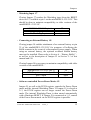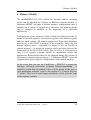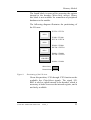
1
miniMODUL-535/515C Hardware-Manual Edition June 1999 A product of a PHYTEC Technology Holding company miniMODUL-535/515C In this manual are descriptions for copyrighted products which are not explicitly indicated as such. The absence of the trademark () symbol does not infer that a product is not protected. Additionally, registered patents and trademarks are similarly not expressly indicated in this manual The information in this document has been carefully checked and is believed to be entirely reliable. However, PHYTEC Meßtechnik GmbH assumes no responsibility for any inaccuracies. PHYTEC Meßtechnik GmbH neither gives any guarantee nor accepts any liability whatsoever for consequential damages resulting from the use of this manual or its associated product. PHYTEC Meßtechnik GmbH reserves the right to alter the information contained herein without prior notification and accepts no responsibility for any damages which might result. Additionally, PHYTEC Meßtechnik GmbH offers no guarantee nor accepts any liability for damages arising from the improper usage or improper installation of the hardware or software. PHYTEC Meßtechnik GmbH further reserves the right to alter the layout and/or design of the hardware without prior notification and accepts no liability for doing so. Copyright 1999 PHYTEC Meßtechnik GmbH, D-55129 Mainz. Rights including those of translation, reprint, broadcast, photomechanical or similar reproduction and storage or processing in computer systems, in whole or in part are reserved. No reproduction may occur without the express written consent from PHYTEC Meßtechnik GmbH. Address: EUROPE NORTH AMERICA PHYTEC Technologie Holding AG Robert-Koch-Str. 39 D-55129 Mainz GERMANY PHYTEC America LLC 255 Ericksen Avenue NE Bainbridge Island, WA 98110 USA Ordering +49 (800) 0749832 Information: [email protected] +1 (800) 278-9913 [email protected] Technical Support: +49 (6131) 9221-31 [email protected] +1 (800) 278-9913 [email protected] Fax: +49 (6131) 9221-33 +1 (206) 780-9135 Web Site: http://www.phytec.de http://www.phytec.com 7th Edition: June 1999 PHYTEC Meßtechnik GmbH 1999 L-230e_7 Contents Preface ...........................................................................................................1 1 Introduction to the miniMODUL-535/515C .....................................3 1.1 Block Diagram..............................................................................5 1.2 miniMODUL-535/515C Overview ..............................................6 2 Pin Description.....................................................................................7 3 Jumpers ..............................................................................................11 3.1 Battery Buffer of U5 J2 .............................................................13 3.2 Serial Interface Configuration J3 and J4 ...................................13 3.3 Special Features ..........................................................................14 3.4 CAN Interface Configuration J11, J12 and J13 (only with miniMODUL-515C) ...................................................................17 4 Memory Models .................................................................................19 4.1 Control Register 1.......................................................................21 4.2 Control Register 2.......................................................................26 4.3 Address Register.........................................................................27 4.4 Mask Register .............................................................................28 5 Flash-Memory....................................................................................31 6 Battery Buffer ....................................................................................33 7 Technical Specifications....................................................................35 8 Hints for Handling the Module ........................................................37 Appendix: Revisions for miniMODUL-535/515C ..................................39 Index ............................................................................................................41 PHYTEC Meßtechnik GmbH 1999 L-230e_7 miniMODUL-535/515C Index of Figures and Tables Figure 1: Block Diagram.............................................................................. 5 Figure 2: miniMODUL-535/515C Overview (Component Side)................ 6 Figure 3: miniMODUL-535/515C Overview (Soldering Side)................... 6 Figure 4: miniMODUL-535/515C Pinout.................................................... 8 Figure 5: Numbering of the Jumper Pads .................................................. 11 Figure 6: Jumper Location (bottom view) ................................................. 11 Figure 7: Default Memory Model after Hardware-Reset........................... 20 Figure 8: Memory Model for Flash-Programming .................................... 22 Figure 9: Partitioning of the I/O-Area ....................................................... 23 Figure 10: Example of a Memory Model..................................................... 30 Figure 11: Memory Areas of the Flash Device............................................ 31 Figure 12: Mechanical Dimensions ............................................................. 35 Table 1: Pinout of the miniMODUL-Connector ........................................ 9 Table 2: Jumper Settings .......................................................................... 12 Table 3: Revisions .................................................................................... 40 PHYTEC Meßtechnik GmbH 1999 L-230e_7 Preface Preface This miniMODUL-535/515C User’s Manual describes the board’s design and functions. Precise specifications for the C515/C515A/ C515C microcontrollers can be found in the enclosed microcontroller Data-Sheet/User’s Manual. If software is included please also refer to additional documentation for this software. In this hardware manual and in the attached schematics, low active signals are denoted by a "/" in front of the signal name (i.e.: /RD). A "0" indicates a logic-zero or low-level signal, while a "1" represents a logic-one or high-level signal. Declaration regarding EMV-Conformity of the PHYTEC miniMODUL-535/515C PHYTEC Single Board Computers (henceforth products) are designed for installation in electrical appliances or as dedicated Evaluation Boards (i.e.: for use as a test and prototype platform for hardware/software development) in laboratory environments. Attention! PHYTEC products lacking protective enclosures are subject to damage by ESD and, hence, may only be unpacked, handled or operated in environments in which sufficient precautionary measures have been taken in respect to ESD-dangers. It is also necessary that only appropriately trained personnel (such as electricians and engineers) handle and/or operate these products. Moreover, PHYTEC products should not be operated without protection circuitry if connections to the product’s pin header rows are longer than 3 m. PHYTEC Meßtechnik GmbH 1999 L-230e_7 1 miniMODUL-535/515C PHYTEC products fulfill the norms of the EMVG-statute only in accordance to the descriptions and rules of usage indicated in this hardware manual (particularly in respect to the pin header row connectors, power connector and serial interface to a host-PC). Implementation of PHYTEC products into target devices, as well as user modifications and extensions of PHYTEC products, is subject to renewed establishment of conformity to, and certification of, EMVStatutes. Only after doing so the devices are allowed to be put into circulation. The miniMODUL-535/515C is one of a series of PHYTEC nano/micro/miniMODULs which can be fitted with different controllers and, hence, offers various functions and configurations. PHYTEC supports all common 8- and 16-bit controllers in two ways: (1) as the basis for Starter Kits in which user-designed hardware can be implemented on a wrap-field around the controller and (2) as insert-ready, fully functional micro- and miniMODULS which can be embedded directly into the user’s peripheral hardware design. PHYTEC’s microcontroller modules allow engineers to shorten development horizons, reduce design costs and speed project concepts from design to market. Please contact PHYTEC for additional information: EUROPE NORTH AMERICA Address: PHYTEC Technologie Holding AG Robert-Koch-Str. 39 D-55129 Mainz GERMANY PHYTEC America LLC 255 Ericksen Avenue NE Bainbridge Island, WA 98110 USA Web Site: http://www.phytec.de http://www.phytec.com e-mail: [email protected] [email protected] Voice: +49 (6131) 9221-0 +1 (800) 278-9913 Fax: +49 (6131) 9221-33 +1 (206) 780-9135 2 PHYTEC Meßtechnik GmbH 1999 L-230e_7 Introduction 1 Introduction to the miniMODUL-535/515C The miniMODUL-535/515C is a credit card-sized Single Board Computer based on the C515, C515A and C515C microcontrollers from Infineon. Its universal design allows its insertion in a wide range of embedded applications. All controller signals and ports extend from the controller to standard-width (2.54 mm.) pin rows aligning three edges of the board, allowing it to be plugged into a target application like a “big chip”. The miniMODUL-535/515C is pre-configured and equipped with all necessary connectors required for immediate start-up (refer to Figure 2 and Figure 3). Precise specifications for the specific controller fitted on the board can be found in the enclosed microcontroller User’s Manual. The descriptions in this manual are based on the C515C/515A/535 controllers. No description of compatible microcontroller derivative functions are included, as such functions are not relevant for basic functioning of the miniMODUL-535/515C. PHYTEC Meßtechnik GmbH 1999 L-230e_7 3 miniMODUL-535/515C The miniMODUL-535/515C offers the following features: • • • • • • • • • • • • • • • • 4 SBC in credit card-size dimensions (55 x 85 mm) achieved through advanced SMD technology fitted with Infineons’ C515/515A/515C 8051-compatible controllers improved interference safety through multi-layer technology controller signals and ports extend to standard-width (2.54 mm.) pins aligning board edges, allowing the board to be plugged into any target application like a “big chip” requires a single low power supply 5 V/typ. < 100 mA 128 (to 512) kByte Flash on-board (PLCC) on-board Flash programming no dedicated Flash programming voltage required through use of 5 V Flash devices 32 (to 160) kByte RAM on-board (SMD) 32 kByte EEPROM (SMD) can also be accommodated on the board flexible software-configured address decoding through complex logic device bank latches for Flash and RAM integrated in address decoder RS-232 interface CAN-Interface (if fitted with the C515C) 3 free Chip-Select signals for easy connection external peripherals operates within a standard range of 0 to 70 degrees C°. PHYTEC Meßtechnik GmbH 1999 L-230e_7 Introduction 1.1 Block Diagram RA M (32 K B ) E EPROM (8/32 / 64K B ) FL A SH (128 / 512 K B ) m BATTERY opt. RA M (32/128 K B ) i n i opt. Ct r l /A d d r Dat a Ct r l /A d d r Dat a M O P2 / Cntrl P0 D Latch Decoder U L d i g i t al I/O-Po rt s INFINION 80C535 / 80C515A / C515C/ an al o g I-Po rt s C RS232 Transceiver asyn c o n n only miniMODUL-515C e c C A N Transceiver as yn c Re s e t / W at c h d o g Figure 1: t o r Block Diagram PHYTEC Meßtechnik GmbH 1999 L-230e_7 5 miniMODUL-535/515C 1.2 miniMODUL-535/515C Overview 33 64 66 65 67 79 80 1 Figure 2: 32 miniMODUL-535/515C Overview (Component Side) 33 64 66 65 67 79 80 32 Figure 3: 6 1 miniMODUL-535/515C Overview (Soldering Side) PHYTEC Meßtechnik GmbH 1999 L-230e_7 Pin Description 2 Pin Description Please note that all module connections are not to exceed their expressed maximum voltage or current. Maximum signal input values are indicated in the corresponding controller manuals/data sheets. As damage from improper connections varies according to use and application, it is the user’s responsibility to take appropriate safety measures to ensure that the module connections are protected from overloading through connected peripherals. As Figure 4 indicates, all controller signals extend to standard-width (2.54 mm) pin rows lining three sides the board (referred to as miniMODUL-Connector). This allows the board to be plugged into any target application like a “big chip”. Many of the controller port pins accessible at the edges of the board have been assigned alternate functions that can be activated via software. Table 1 provides an overview of the pinout of the miniMODULConnector, as well as hints about additional functions of some of the port pins. For further details please refer to the User Manual of the C515 or C515C. Attention: The miniMODUL-535/515C has been reengineered for Flash technology in an manner ensuring the highest possible compatibility to earlier non-Flash fitted versions of the miniMODUL-535. However some differences in pinout to earlier versions, as described in the Appendix: Revisions for miniMODUL-535/515C, were unavoidable. PHYTEC Meßtechnik GmbH 1999 L-230e_7 7 miniMODUL-535/515C 33 64 66 65 67 79 80 1 Figure 4: 8 32 miniMODUL-535/515C Pinout PIN # 1 2...9 10...17 18...23 24 25 26 27 28 29 30 31 32 Connection NC / WDI P4.0...P4.7 P5.0...P5.7 P1.0...P1.5 P1.6 / P4.6 P1.7 P3.0 RXD P3.1 TXD P3.2 INT0 P3.3 INT1 P3.4 T0 /RES NC / VBAT 33 34 35 36...39 40...47 VCC VPD P3.5 / T1 A11...A8 A7...A0 Comments optional Watchdog-Input Port 4 Port 5 Port 1 Port 1.6 / 4.6 via Jumper J11 Port 1.7 Port 3.0 or RXD (RS-232) Port 3.1 or TXD (RS-232) Port 3.2 or INT0 Port 3.3 or INT1 Port 3.4 or Timer 0 /Reset-Input of the module optional external battery buffer via Jumper J8 power supply +5 V DC battery voltage output Port 3.5 or Timer 1 address bus (High-Byte) address bus (Low-Byte) PHYTEC Meßtechnik GmbH 1999 L-230e_7 Pin Description /PFO / P4.7 / power-Fail-Output , P4.7 or CANH1 via CANH Jumper J13 49 /HPD / CANL optional /HWPD-Input2 or CANL1 via Jumper J12 50 /PSEN program-Store-Enable-Output 51 P3.6 / /WR Port 3.6 or /WR-Signal 52 P3.7 / /RD Port 3.7 or /RD-Signal 53 /CS3 pre-decoded Chip-Select-Signal #3 54 /CS2 pre-decoded Chip-Select-Signal #2 55 /CS1 pre-decoded Chip-Select-Signal #1 56...63 D7...D0 data bus (controller port 0) 64 GND ground 0V. 65 AREF analog reference voltage +5 V DC 66,68,70,72,7 AN7...AN0 8 analog inputs 4,76,78,80 67,69,71,73,7 AGND analog ground (GND) 0 V 5,77,79 48 Table 1: 1: 2: Pinout of the miniMODUL-Connector only with C515C microcoller only with C515A microcoller PHYTEC Meßtechnik GmbH 1999 L-230e_7 9 miniMODUL-535/515C 10 PHYTEC Meßtechnik GmbH 1999 L-230e_7 Jumpers 3 Jumpers For configuration purposes, the miniMODUL-535/515C has 13 soldering jumpers, some of which have been configured prior to delivery. Figure 5 illustrates the numbering of the jumper-pads, while Figure 6 indicates the location of the jumpers on the miniMODUL. All soldering jumpers (Jxx) on the miniMODUL-535/515C are located on its bottom side. 1 2 3 1 1 2 Figure 5: Numbering of the Jumper Pads Figure 6: Jumper Location (bottom view) PHYTEC Meßtechnik GmbH 1999 L-230e_7 2 4 3 11 miniMODUL-535/515C The jumpers (J = solderable jumper) have the following functions: Default-Setting Alternate-Setting (1+2) external ROM/ Flash (2+3) internal ROM/Flash acactive tive (1+2) no battery buffer (2+3) U5 buffered by battery (only for RAM-devices) (1+2) pins 26 and 27 carry (2+3) pins 26 and 27 carry (1+2) RS-232 signals from (2+3) TTL signals from the the on-board controller’s serial port transceiver (open) VAREF and (closed) VAREF and (closed) VAGND derived (open) VAGND derived from from supply voltage externall voltage source via miniMODULConnector (open) Watchdog input not (closed) Watchdog input available connected to pin 1 of the miniMODUL-Connector (open) pin 32 of the (closed) VBAT input connected miniMODULto pin 32 of the Connector is open miniMODUL-Connector (1+2) Power-Down with (2+3) Power-Down with Register PCON Register PCON disabled, enabled, WatchdogWatchdog-Timer enabled Timer disabled 1 (1+2) Power-Down Mode (2+3)1 Power-Down Mode of of external memory external memory disabled enabled 2 Power-Down Mode (2+3) of external memory disabled (1+2) Pin 24 is connected Refer to section 3.3 and 3.4 to see (2+3) to port P1.6, pin 49 other configurations (2+3) carries CANL and pin 48 CANH J1 J2 J3, J4 J5, J6 J7 J8 J9 J10 J11 J12 J13 Table 2: 1: 2: 12 Jumper Settings only for C515-derivatives with /CPUR-output (e.g. C515C) all other C515-derivatives without /CPUR-output PHYTEC Meßtechnik GmbH 1999 L-230e_7 Jumpers 3.1 Battery Buffer of U5 J2 Jumper J2 configures the power supply for the memory device installed at U5. If an EEPROM is fitted at U5, a Vcc supply is necessary (i.e., J2 should be closed at 1+2) to prevent discharge of the battery buffer. If U5 is populated with a RAM device, the power should be supplied via VPD (i.e., J2 should be closed at 2+3) in order to preserve data by means of the battery buffer in the absence of a power supply via Vcc. Device type at U5 EEPROM RAM J2 1+2 2+3 Attention: The battery device on the miniMODUL-535/515C is not appropriate to supply an EEPROM if installed at U5. Therefore jumper J2 has to be closed at 1+2 in order to avoid fast discharge of the battery. 3.2 Serial Interface Configuration J3 and J4 With Jumpers J3 and J4, different serial interface signal levels and signal qualities can be configured at pins 26 and 27 of the miniMODUL-535/515C. These pins carry either the TTL-signals of the controller’s serial interface or the signals of the on-board RS-232 transceiver. At the time of delivery the RS-232 interface is active by default. The following signal levels and qualities can be configured: Signal Quality RS-232 TTL PHYTEC Meßtechnik GmbH 1999 L-230e_7 J3 1+2 2+3 J4 1+2 2+3 13 miniMODUL-535/515C 3.3 Special Features Jumpers J1, J5, J6, J7, J8, J9, J10, J12 and J13 are used to activate the special features of the particular controller fitted on the module. - Execution out of Internal or External Program Memory J1 At the time of delivery Jumper J1 is pre-connected at pads 1+2. This default configuration means that the program stored in the external program memory is executed after a hardware-RESET. In order to allow the execution of a specific controller’s internal program memory the pads 2+3 on jumper J1 must be connected. The following configurations are possible: Code-access External Program Memory Internal Program Memory J1 1+2 2+3 - Reference Voltage of the A/D Converter J5 and J6 The A/D converter requires a reference voltage (VAREF, VAGND) applied at pins 3 and 4 of the controller. This reference voltage can be derived either from an external source connected to the miniMODUL-Connector at pin 65 (VAREF) and pins 67, 69, 71, 73, 75, 77, 79 (VAGND) or from the supply voltage of the miniMODUL-535/515C. The source of the reference voltage can be chosen with jumpers J5, (VAREF) and J6, (VAGND). Selecting the miniMODUL’s supply voltage as reference voltage leads to a common supply for digital and analog signals. These jumpers are at a central point in analog circuitry which results in minimal interference. Analog supply via digital supply external supply 14 J5 closed open J6 closed open PHYTEC Meßtechnik GmbH 1999 L-230e_7 Jumpers - Watchdog Input J7 Closing Jumper J7 renders the Watchdog input from the RESET device at U7 available at pin 1 on the miniMODUL-535/515C. This should be done to maintain compatibility to older versions of the miniMODUL-535/515C. miniMODUL-535/515C pin 1 Watchdog Input No Watchdog Input J7 closed open - Connecting an External Battery J8 Closing jumper J8 enables attachment of an external battery at pin 32 of the miniMODUL-535/515C for purposes of buffering the RAM contents in the event of a disconnected power supply. When using an external battery, the optional on-board lithium battery must not be installed. Please refer to Section 6 – “Battery Buffer” – as well as to the description of Jumper J2 in Section 3.1 of this manual and J10. Closing Jumper J8 is necessary to maintain compatibility with older versions of the miniMODUL. miniMODUL-535/515C pin 32 VBAT input connected to pin 32 pin 32 open J8 closed open - Software-controlled Power-Down Modes J9 Jumper J9, as well as the PCON register, controls the Power-Down mode and the internal Watchdog-Timer. If Jumper J9 is closed at 2+3, the PCON register can no longer control the Power-Down mode. The internal Watchdog-Timer is then started automatically with a Hardware-RESET. If Jumper J9 is connected at 1+2, control of the Power-Down mode via the PCON register is possible. PHYTEC Meßtechnik GmbH 1999 L-230e_7 15 miniMODUL-535/515C The internal Watchdog-Timer can then no longer be started with a Reset. Power-Down with PCON Enabled Disabled Watchdog-Timer disabled enabled - Power Saving Mode for (only for miniMODUL-515C) External J9 1+2 2+3 Memory J10, With Jumper J10, the C515C controller’s /CPUR output can be used to force the external memory into a Power-Save mode. This means that external memory, which is otherwise only briefly deactivated during a Hardware-RESET, is also deactivated during the controller Power-Down. External Memory Power-Down Mode enabled disabled J10 1+2 2+3 Attention: It is not possible to use /CPUR-signal and a battery buffer at the same time. If a battery buffer is used the External Memory Power Down Mode must be disabled (JP10 at 2+3), otherwise the battery will be discharged. - /HPD and /PFO J11 and J12, The Jumpers J11 and J12 connect the controller hardware PowerDown-input with the Watchdog Power-Failure-output at pins 48 and 49. 16 /HPD on pin 49 J12 1+2 /PFO on pin 48 J13 1+2 PHYTEC Meßtechnik GmbH 1999 L-230e_7 Jumpers Please note that with a miniMODUL fitted with the C515C controller, the CAN-interface can also be connected via jumper J12 and J13 to the pins 48 and 49. In this case /PFO and /HPD are not available on the miniMODUL-515C. 3.4 CAN Interface Configuration J11, J12 and J13 (only with miniMODUL-515C) The C515C’s CAN-interface is available at port pins P4.6 and 4.7. These signals extend to the CAN-transceiver populating U9 (PCA82C250 or Si9200), which generates the signals CAN_H (at pin 48) and CAN_L (at pin 49). These signals can be directly connected to a CAN-bus using a dual-wire cable. If no CAN-transceiver populates U9, the controller signals TxDC and RxDC are accessible at pins 48 and 24 for use with an external transceiver. In both modes (on-board or external transceiver) the miniMODUL535/515C is pin-compatible to PHYTEC’s CANmodul-592. For detailed descriptions of the CAN-interface please refer to appropriate controller User’s Manual from Infineon, as well as accompanying CAN Addenda. The following configurations are possible: CAN Driver External CAN Driver Internal CAN Driver (U9 populated) J11 2+3 1+2 J12 1+2 2+3 J13 2+4 2+3 Please note that the signals /HPD, and /PFO, can also transmit via pins 48 and 49 by configuring jumpers J12 and J13. In this case, these signals are not additionally available for use with the CAN interface on the miniMODUL fitted with the C515C. PHYTEC Meßtechnik GmbH 1999 L-230e_7 17 miniMODUL-535/515C 18 PHYTEC Meßtechnik GmbH 1999 L-230e_7 Memory Models 4 Memory Models The miniMODUL-535/515C allows for flexible address decoding which can be adjusted by software to different memory-models. A Hardware-RESET activates a default memory configuration that is suitable for a variety of applications. However, this memory-model can be changed or adjusted at the beginning of a particular application. Configuration of the memory is done within the address decoder by means of internal registers: two control registers, one address register and one mask register. All named registers are Write-Only-Registers with access to the XDATA-memory of the controller. There are two distinct address areas - selectable by means of the bit IO-SW in control register 1 - by which the registers can be accessed (refer to the description of the bit IO-SW below). Due to a lack of read-access, a copy of all register contents should be maintained within the application. Reserved bits may not be changed during the writing of the register; contents must remain at 0. A Hardware-RESET erases all registers while preserving the configuration of the default memory. In the event that you use the FlashTools – PHYTEC’s proprietary firmware allowing convenient on-board Flash-programming - it should be noted that the address FA16 will be preset at the start of your application software (refer to the section 4.1 "Control Register 1" below). This is to be noted upon installation of the software copy of the register contents. PHYTEC Meßtechnik GmbH 1999 L-230e_7 19 miniMODUL-535/515C The following figure displays the default memory model: CODE XDATA I/O FFFFH RAM or EEPROM U5 (optional) 8000H 7FFFH Flash U3 RAM U4 0000H PRG-EN = 0 VN-EN = 0 IO-SW = 0 Figure 7: Default Memory Model after Hardware-Reset It should be noted that the memory blocks U4 and U5 comprise separate 32 kByte memory areas in the XDATA address-area of the controller. The standard module houses a single 32 kByte RAM device at U4. In the event that a 128 kByte RAM device is installed at U4, then blocks of 32 kByte can be accessed and switched via banklatching. In the event that memory devices do not populate U4 and U5, then there is no possible access to the corresponding XDATA memories. The corresponding current I/O-area is concentrated in an XDATA-address area in which there is no access to any existing RAM. The following sections explain the registers of the address decoder for configuration of the memory: 20 PHYTEC Meßtechnik GmbH 1999 L-230e_7 Memory Models 4.1 Control Register Control Register 1 (Address 7C00H / FC00H) Bit 7 Bit 0 PRG- IO-SW RAM- VN-EN FA18 FA17 FA161 FA15 EN SW Bit invalid in programming-model (refer to PRG-EN) Bit valid only in programming-model (refer to PRG-EN) PRG-EN: Activates the special Flash-programming memory model (PRG-EN = 1). This configuration is used within FlashTools2 for Flash-programming. On account of existing restrictions it is either of no or of restricted use in the user’s application. In this model, 32 kByte Flash memory located within the address range 0000H - 7FFFH is accessible, as well as 32 kByte RAM within the range 8000H - FFFFH. The Flash memory can only be written in the XDATAarea and can only be read from the CODE-area. The RAM can be read from and written to in the XDATAarea. RAM can also be read from the CODE-area. The address line A15 of the Flash is derived from the Control Register 1 (Bit 0, FA15) only in the programming configuration. In the Runtime executionconfiguration (PRG-EN = 0), the address line A15 of the controller leads directly to the Flash device. The bit IO-SW is also relevant to the programming configuration; whereas the bit VN-EN is not relevant. 1: 2: In the event that you use the FlashTools - a firmware allowing convenient on-board Flash-programming - it should be noted that the address FA16 will be preset at the start of your application software. This is to be noted upon installation of the software copy of the register contents. PHYTEC firmware allowing convenient on-board Flash-programming. Upon delivery of the module, this firmware is already resident in the Flash device. PHYTEC Meßtechnik GmbH 1999 L-230e_7 21 miniMODUL-535/515C The following figure illustrates the programming configuration (the I/O-field is not represented): CODE XDATA FFFFH RAM U4 8000H 7FFFH Flash U3 0000H PRG-EN = 1 RAM-SW = 1 Read-Only Write-Only Read-Write Figure 8: IO-SW: Memory Model for Flash-Programming By means of this bit, the I/O-area of the module can be selectively mapped either to the upper or to the lower 32 kByte of the address space. After a Hardware-Reset (IO-SW = 0) the I/O-area is located in the address area from FC00H to FFFFH. Following setting of the IOSW-bit, the I/O-area is located in the address area from 7C00H to 7FFFH. This I/O-area generally consists of 4 blocks of 256 bytes. In three of these blocks the address decoder provides a pre-coded Chip-Select signal which simplifies the connection of peripheral hardware to the module. These Chip-Select signals are activated by XDATAaccess (Read-Write access) to the corresponding address area. 22 PHYTEC Meßtechnik GmbH 1999 L-230e_7 Memory Models The fourth block is reserved for accessing the register internal to the decoder (Write-Only access). Hence, this block is not available for connection of peripheral hardware to the module. The following diagram illustrates the partitioning of the I/O-area: 7FFFH / FFFFH /CS3 7F00H / FF00H 7EFFH / FEFFH /CS2 7E00H / FE00H 7DFFH / FDFFH /CS1 7D00H / FD00H 7CFFH / FCFFH /CS-REG 7C00H / FC00H W rite-Only Read-W rite Figure 9: Partitioning of the I/O-Area Given this partition, /CS1 through /CS3 function as the available free Chip-Select signals. The signal /CSREG is solely a signal internal to the decoder, which is necessary in order to access the internal register, and is not freely available. PHYTEC Meßtechnik GmbH 1999 L-230e_7 23 miniMODUL-535/515C Connection of peripheral devices to the area of /CSREG should not take place under any circumstances in order to maintain the correct function of the FlashTools1 for programming of the Flash. The internal register is to occupy only the address ranges 7C00H 7C03H and/or FC00H - FC03H. The rest of the /CSREG block remains unused and is reserved for future expansion. RAM-SW: This bit enables exchange of 32 kByte memory areas of the devices installed at U4 and U5. Following a Hardware-Reset (RAM-SW = 0) the RAM U4 is mirrored in the area from 0000H to 7FFFh and the RAM/EEPROM at U5 is addressable from 8000H to FFFH. After setting the RAM-SW bit, the RAM at U4 populates the area from 8000H-FFFFH. Likewise, the RAM/EEPROM at U5 populates the area from 0000H7FFFH. In the corresponding I/O areas, there is no access to the memory devices. VN-EN: This bit enables free selection of von-Neumann memory2 within the address space of the controller. A Reset renders a Harvard3-Architecture available as the default configuration. Von-Neumann memory is especially useful when programming code is to be downloaded and subsequently run during Runtime, as is the case with a Monitor program. The location of the optional von-Neumann memory is defined through the address- and mask registers (see below). 1: 2: 3: 24 PHYTEC firmware allowing convenient on-board Flash-programming. Upon delivery of the module, this firmware is already resident in the Flash device. Memory area in which no difference is made between CODE- and XDATA-access. This means that both accesses use the same physical memory device, usually a RAM. Memory area in which CODE and XDATA-accesses use physical different memory devices. CODE-access typically uses a ROM or Flash device, whereas XDATAaccess uses a RAM. PHYTEC Meßtechnik GmbH 1999 L-230e_7 Memory Models Following a Hardware-Reset (VN-EN = 0) the settings in the address- and mask registers are not released, which means that no von Neumann-memory is available. After setting the bit (VN-EN = 1), the settings in the address- and mask registers are valid and incorporated in access addressing. This bit is only relevant in the Runtime-model (PRG-EN = 0). In the Programming-model (PRG=1) it is unimportant and ignored. FA[18..15]: The module can be equipped with an optional 512 kByte Flash memory. As the controller’s address space is limited to 64 kByte, the remainder of the Flash memory can only be accessed by means of bank memory switching. In the Runtime-model (PRG-EN = 0), 64 kByte banks can be switched by controlling the high address lines A[18..16] for the Flash through software. For this purpose, register bits FA[18..16] of the address decoder provide a latch to which the desired higher addresses can be written. Of particular note is the bit FA15, which is solely relevant in the programming-model (PRG-EN = 1). As only 32 kByte of Flash can be accessed in this model, it serves as address line A15 for the Flash memory. In the Runtime-model (PRG-EN = 0) with a 64 kByte Flash memory area, to contrast, the addres line A15 of the controller is attached directly to the Flash. Bits FA[18..16] are dependent on the hardware configuration of the module and function as described above only if Flash devices of at least 512 kByte are installed on the board. PHYTEC Meßtechnik GmbH 1999 L-230e_7 25 miniMODUL-535/515C 4.2 Control Register 2 Control Register 2 (Address 7C01H / FC01H) Bit 7 N/A1 N/A N/A N/A N/A N/A Bit 0 RA16 RA15 RA[16.. 15]: The module can optionally accommodate a 128 kByte RAM device at U4. As the address space at U4 is limited to 32 kByte in the XDATA area of the controller, the remainder of the RAM can only be accessed by means of bank switching. Four memory banks of 32 kByte banks can be switched by setting the high address-lines A[16..15] through software. For this purpose, register bit RA[16..15] of the address decoder provides a latch to which the desired higher addresses can be written. The function of this bit is dependent on the hardware configuration of the module and functions, as described above, only in connection with RAM devices of at least 128 kByte at U4. 1: 26 N/A: Not Accessible PHYTEC Meßtechnik GmbH 1999 L-230e_7 Memory Models 4.3 Address Register The address register 7C02H / FC02H functions in conjunction with the mask register (see below) to define the von-Neumann 1- and Harvard2-memory in the controller’s addressing area. By setting the bit VN-EN in control register 1, the values of the address and the mask register become valid for the definition of the von-Neumann and the Harvard addressing space and are used for address decoding (refer to Control Register 1). The location of one or more Harvard areas can be configured with both registers. The remaining sections of the addressing area are configured as von-Neumann area in which RAM is accessible through XDATA as well as through CODE. The mechanism through which the areas are differentiated is based on a comparison of the current address with a predefined address pattern of variable width. If the relevant bit positions of the addresses conform to one another, access occurs according to the Harvardarchitecture. In the case of nonconformity, access occurs according to the von-Neumann-architecture. Address Register (Address 7C02H / FC02H) Bit 7 HA15 HA14 HA13 HA12 HA11 HA10 Res.3 Bit 0 Res. The address register holds the address pattern mentioned above. Each bit of the pattern is compared with the corresponding address line of the controller (HA15 with A15, ..., HA10 with A10). As address lines A15 .. A10 are used to define Harvard addressing space, only Harvard-fields of at least 1 kByte can be configured. Areas smaller than 1 kByte can not be configured. 1: 2: 3: Memory area in which no difference exists between CODE- and XDATA-access. This means that both accesses use the same physical memory device, usually a RAM. Memory area in which CODE and XDATA-accesses use different physical memory devices. Usually CODE-access uses a ROM or Flash device, whereas XDATAaccess uses a RAM. Reserved bits are not to be changed, the default value (0) must remain. PHYTEC Meßtechnik GmbH 1999 L-230e_7 27 miniMODUL-535/515C 4.4 Mask Register The mask register (addresses 7C03H / FC03H) serves the masking of single bits in the address register (see above). Following a HardwareReset, all bits within the address register are relevant. By setting the individual bits in the mask register, all corresponding bits in the address register will no longer be subject to an address comparison. Mask Register (Address 7C03H / FC03H) Bit 7 MA15 MA14 MA13 MA12 MA11 MA10 Res.1 Bit 0 Res. Please note that in the case of a board populated with a single 32 kByte RAM, the memory area is mirrored within the controller’s addressing area. On account of the insufficient utilization of A15 in this configuration, memory accesses to addresses higher than 8000H are reduced to accesses to the memory area from 0000H to 7FFFH. This should be taken into consideration when choosing the memorymodel. Otherwise, function failure could result from overlapping access. 1: 28 Reserved bits are not to be changed, the default value (0) must remain. PHYTEC Meßtechnik GmbH 1999 L-230e_7 Memory Models The following examples of different combinations of the address- and mask registers illustrate these functions (X = specific bit irrelevant): Address-Reg. 1XXXXX00 b Mask-Reg. 01111100b 0XXXXX00 b 01111100b 11111100 b 00000000b 010X0000 b 00010000b 10000000 b 00000000b 10100X00 b 00000100b Comments (only for VN-EN = 1) Harvard 8000H-FFFFH, Von-Neumann 0000H-7FFFH Harvard 0000H-7FFFH, Von-Neumann 8000H-FFFFH Harvard FC00H-FFFFH, Von-Neumann 0000H-FBFFH Harvard 4000H-43FFH and 5000H-53FFH, Von-Neumann 0000H-3FFFH, 4400H-4FFFH and 5400H-FFFFH Harvard 8000H-83FFH, Von-Neumann 0000H-7FFFH and 8400H-FFFFH Harvard A000H-A7FFH, Von-Neumann 0000H-9FFFH and A800H-FFFFH Reserved bits without function for address decoding (refer to description of the register) X = irrelevant (on account of a bit set in the mask register)The last example in the table is further illustrated by the following figure: PHYTEC Meßtechnik GmbH 1999 L-230e_7 29 miniMODUL-535/515C CODE XDATA I/O FFFFH Von-Neumann Flash U3 RAM U5 A800H A7FFH A000H 9FFFH 8000H 7FFFH Harvard Von-Neumann RAM U4 0000H PRG-EN = 0 VN-EN = 1 IO-SW = 0 RAM-SW = 0 Addr.-Reg. = 10100X00b Mask.-Reg. = 00000100b Figure 10: 30 Example of a Memory Model PHYTEC Meßtechnik GmbH 1999 L-230e_7 Flash-Memory 5 Flash-Memory Flash is a highly functional means of storing non-volatile data. Having the miniMODUL-535/515C equipped with a Flash device this modern technique is at your disposal. The miniMODUL-535/515C can house a Flash device of type 29F010 with two banks of 64 kByte each or of type 29F040 with 8 banks of 64kByte each. Use of Flash devices allows incorporation of on-board programming capability. The Flash devices are programmable with 5V=. Consequently, no dedicated programming voltage is required. A firmware to programm the Flash device (the so-called FlashTools) is pre-installed in the first bank (bank 0) of the Flash device. Hence the total memory available is 64 kByte or 448 kByte (refer to Figure 11). Should this software be erased from the Flash device without having a back-up or an equivalent replacement, reprogramming is no longer possible! FFFFH 29F010 FFH bank 0 bank 1 FFFFH 8000H 7FFFH 8000H 7FFFH 0000H 0000H 29F040 H bank 0 bank 1 bank 2 bank 3 bank 4 bank 5 bank 6 bank 7 FlashTools firmware (software protected) Figure 11: Memory Areas of the Flash Device PHYTEC Meßtechnik GmbH 1999 L-230e_7 31 miniMODUL-535/515C Please note that this firmware protects itself against any intentional or accidental erasure or copy-over. As the Flash device’s hardware protection mechanism is not utilized, protection is limited to the software level. In the event that you might wish to download your own programming algorithms or tools into the Flash, please ensure that a programming tool remains in the Flash memory. Refer to the “QuickStart Instructions" for a detailed description of the on-board programming. Use of a Flash device as the only code memory results in no or only a limited usability of the Flash memory as non-volatile memory for data. This is due to the internal structure of the Flash device as, during the Flash-internal programming process, the reading of data from Flash is not possible. Hence, for Flash programming, program execution must be transferred out of Flash (such as into von-Neumann RAM). This usually equals the interruption of a "normal" program execution cycle. As of the printing of this manual, Flash devices generally have a life expectancy of at least 100,000 Erase-/Program-cycles. 32 PHYTEC Meßtechnik GmbH 1999 L-230e_7 Battery Buffer 6 Battery Buffer The battery that buffers the memory is not otherwise essential to the functioning of the miniMODUL-535/515C. However, this battery buffer embodies an economical and practical means of storing nonvolatile data. The VBAT-input at pin 32 is intended to connect to an external battery. Optionally a battery can be installed at position BAT1 on the component side of the module. As of the pressing of this manual, a lithium battery is recommended for use with the module as it offers relatively high capacity at low discharge. In the event of a power failure at Vcc, the connected battery via VBAT will buffer the RAM memory blocks. Attention: The battery device on the miniMODUL-535/515C is not appropriate to supply an EEPROM if installed at U5. Therefore jumper J2 has to be closed at 1+2 in order to avoid fast discharge of the battery. It is not possible to use /CPUR-signal and a battery buffer at the same time. If a battery buffer is used the External Memory Power Down Mode must be disabled (JP10 at 2+3), otherwise the battery will be discharged. Power consumption depends on the components used and memory size. This is typically < 1 µA. per 32 kByte RAM device installed on the miniMODUL. For reasons of operating safety, please be advised that despite a battery buffer, changes in the data content within the RAM can occur given disturbances. The battery buffer does not completely remove the danger of data destruction. PHYTEC Meßtechnik GmbH 1999 L-230e_7 33 miniMODUL-535/515C 34 PHYTEC Meßtechnik GmbH 1999 L-230e_7 Technical Specifications 7 Technical Specifications The physical dimensions of the miniMODUL-535/515C are represented in Figure 11. The module’s profile is ca. 10 mm. thick, with a maximum component height of 3 mm. on the back-side of the PCB and approximately 5 mm. on the front-side. The board itself is approximately 1.5 mm thick. 3,81m m 5,59m m 5,84m m miniMODUL-535/ 515C 17,78m m 54,90m m D = 3.2m m 5,84m m 5,59m m 1.27m m 3,81m m 0,76m m 2,54m m 78,74m m 85m m Figure 12: 1,27m m Mechanical Dimensions PHYTEC Meßtechnik GmbH 1999 L-230e_7 35 miniMODUL-535/515C Additional specifications: • Dimensions: • Weight: • • • • • • 54.9 x 85 mm., ±0,01mm approximately 44 g with 160 kByte RAM device, socketed Flash device and socket controller; ca. 32 g with standard 32 kByte RAM without socket Storage temperature: -40°C to +90°C Operating temperature: standard 0°C to +70°C, extended -40°C to +85°C Humidity: maximum 95% r.F. not condensed Operating voltage: 5 V. ±5%, VBAT 3V ±20% Power consumption: maximum 140 mA, typ. 100 mA at 12 MHz oscillator frequency and 128 kByte RAM at +20°C Power consumption with battery buffer of maximum 10 µA per RAM-device, typically 1 µA per RAM-device at +20°C These specifications describe the standard configuration of the miniMODUL-535/515C as of the pressing of this manual. Please note that utilizing the battery buffer for the RAMs the storage temperature is only 0°C to +70°C. 36 PHYTEC Meßtechnik GmbH 1999 L-230e_7 Hints for Handling the Module 8 Hints for Handling the Module When changing controllers please ensure that all components remain free from intrusive damage. Any controller used on the module must be pin-compatible with the C515 / C515C, and all special hardware features must be compatible with the layout of the board. Removal of the standard quartz or oscillator is not advisable given the compact nature of the module. Should this nonetheless be necessary, please ensure that the board, as well as surrounding components and sockets, remain undamaged during the unsoldering process. Overheating the board can cause the solder pads to loosen, rendering the module inoperable. Carefully heat neighboring connections in pairs. After a few alternations, components can be removed with the solder-iron tip. Alternatively, a hot air gun can be used to heat and loosen the bonds. PHYTEC Meßtechnik GmbH 1999 L-230e_7 37 miniMODUL-535/515C 38 PHYTEC Meßtechnik GmbH 1999 L-230e_7 Revisions Appendix: Revisions for miniMODUL-535/515C The miniMODUL-535/515C is an extension of the existing miniMODUL-535. The miniMODUL-535/515C has been updated for Flash memory technology. Additionally, the module can now be fitted with Siemen’s C515C and C515A controllers. PHYTEC strives to maintain maximum compatibility between this new and preceding versions of the miniMODUL However, small differences in board configuration between Flash and EPROM versions, as well as between C515x controller derivative versions, were inevitable. These differences are explained in the table below: miniMODUL-535 (Old version: MM-001) miniMODUL-535/515C (New version: MM-003-XX) Pin VCC 1 Pin 32 Pin 48 Vcc extends only to pin 33 in order to improve EMC features. The Watchdog input from U7 can be optionally connected with pin 33 via Jumper J7. GND GND extends only to pin 64 in order to improve EMC features. The Vbat input can be optionally connected with pin 64 via Jumper J8 for an external battery connection. /Low Line-Output has Low- /PFO-Output has Low-level if VBAT level if VCC < 4.6 V. < 2.5 V (dependent upon controller (dependent upon controller threshold) threshold) PHYTEC Meßtechnik GmbH 1999 L-230e_7 39 miniMODUL-535/515C miniMODUL-535 (Old version: MM-001) miniMODUL-535/515C (New version: MM-003-XX) Pin MODE-Input for selection the /HWPD-Input if module is fitted with 49 memory model C515A controller. This input should remain unswitched (internal pull-up) or be connected to Vcc. Optionally a Hardware-Power-Down mode can be achieved by a controlled connection with a Low- level. U3 applicable to house an OTP/ applicable to house a Flash (types EPROM (32 Kx8 /64 Kx8) in 29F010/ 29F040 with 128 Kx8 / (P)LCC-socket 512 Kx8) or OTP (with 128 Kx8) in PLCC socket. Table 3: 40 Revisions PHYTEC Meßtechnik GmbH 1999 L-230e_7 Index Index / I /HPD....................................16, 17 /PFO ....................................16, 17 I/O-Area.....................................23 IO-SW .......................................22 A J Address Decoding .....................19 Address Register .......................27 Analog Supply...........................14 J1 ...............................................14 J10 .............................................16 J11 .......................................16, 17 J12 .......................................16, 17 J13 .............................................17 J2 ...............................................13 J3 ...............................................13 J4 ...............................................13 J5 ...............................................14 J6 ...............................................14 J8 ...............................................15 J9 ...............................................15 Jumper location .........................11 Jumper numbering .....................11 Jumper Settings .........................12 B Battery Buffer......................15, 33 Block Diagram ............................5 C CAN-Interface...........................17 Chip-Select Signals ...................23 Control Register 1 .....................21 Control Register 2 .....................26 D Default Memory Model.............20 M E EMV ............................................1 ESD .............................................1 External Battery.........................15 Mask Register............................28 Memory Model..........................19 miniMODUL-Connector .............7 P F FA[18..15] .................................25 Features .......................................4 Flash Programming Memory Model ........................................22 Flash-Memory ...........................31 H Hints for Handling the Module .37 Physical Dimensions .................35 Pin Description ............................7 Pinout of the miniMODULConnector ....................................9 Power Consumption ..................36 Power Saving.............................15 PRG-EN.....................................21 Program Memory.......................14 R RA16 .........................................26 PHYTEC Meßtechnik GmbH 1999 L-230e_7 41 miniMODUL-535/515C RAM-SW .................................. 24 Reference Voltage..................... 14 Registers of the address decoder ................................................... 20 Revisions................................... 39 RS-232 Transceiver .................. 13 S Serial Interface .......................... 13 Special Features ........................ 14 42 T Technical Specifications ........... 35 V VN-EN ...................................... 24 W Watchdog ............................ 15, 16 PHYTEC Meßtechnik GmbH 1999 L-230e_7 Suggestions for Improvment Document: miniMODUL-535/515C Document number: L-230e_7, January 1999 How would you improve this manual? Did you find any mistakes in this manual? Submitted by: Customer number: Name: Company: Address: Return to: PHYTEC Technologie Holding AG Postfach 100403 D-55135 Mainz, Germany Fax : +49 (6131) 9221-33 PHYTEC Meßtechnik GmbH 1999 L-230e_7 page Published by PHYTEC Meßtechnik GmbH 1999 Ordering No. L-230e_7 Printed in Germany