1
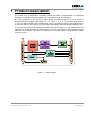
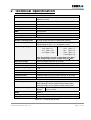
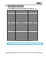
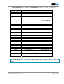
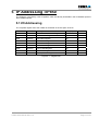
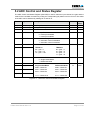
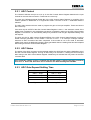
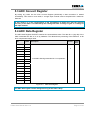
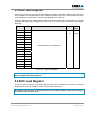
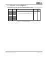
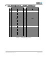
The Embedded I/O Company TIP850 16 Channel 12 bit A/D 4 Channel 12 bit D/A Version 1.2 User Manual Issue 1.9 September 2006 D75850800 TEWS TECHNOLOGIES GmbH Am Bahnhof 7 Phone: +49-(0)4101-4058-0 25469 Halstenbek, Germany Fax: +49-(0)4101-4058-19 www.tews.com e-mail: [email protected] TEWS TECHNOLOGIES LLC 9190 Double Diamond Parkway, Suite 127, Reno, NV 89521, USA www.tews.com Phone: +1 (775) 850 5830 Fax: +1 (775) 201 0347 e-mail: [email protected] TIP850-10 16 Channel 12 bit A/D (gain 1, 10, 100), 4 Channel 12 bit D/A TIP850-11 16 Channel 12 bit A/D (gain 1, 2, 4, 8), This document contains information, which is proprietary to TEWS TECHNOLOGIES GmbH. Any reproduction without written permission is forbidden. TEWS TECHNOLOGIES GmbH has made any effort to ensure that this manual is accurate and complete. However TEWS TECHNOLOGIES GmbH reserves the right to change the product described in this document at any time without notice. 4 Channel 12 bit D/A This manual covers both products TEWS TECHNOLOGIES GmbH is not liable for any damage arising out of the application or use of the device described herein. Style Conventions Hexadecimal characters are specified with prefix 0x, i.e. 0x029E (that means hexadecimal value 029E). For signals on hardware products, an ‚Active Low’ is represented by the signal name with # following, i.e. IP_RESET#. Access terms are described as: W Write Only R Read Only R/W Read/Write R/C Read/Clear R/S Read/Set 1994-2006 by TEWS TECHNOLOGIES GmbH IndustryPack is a registered trademark of SBS Technologies, Inc TIP850 User Manual Issue 1.9 Page 2 of 20 Issue Description Date 1.0 First Issue June 1994 1.1 Change of settling time December 1994 1.2 Change of settling time February 1996 1.3 New Hardware Version 1.2 January 2003 1.4 Addition “Technical Specification” April 2003 1.5 I/O Pin Assignment Corrected July 2003 1.6 Description ID PROM Contents August 2003 1.7 Addition “Technical Specification” April 2004 1.8 Added Programming Note and Installation Note October 2004 1.9 New address TEWS LLC September 2006 TIP850 User Manual Issue 1.9 Page 3 of 20 Table of Contents 1 2 3 PRODUCT DESCRIPTION ......................................................................................... 6 TECHNICAL SPECIFICATION................................................................................... 7 FUNCTIONAL DESCRIPTION ................................................................................... 8 3.1 Analog Input ....................................................................................................................................8 3.2 Analog Output .................................................................................................................................8 3.3 Data Correction ...............................................................................................................................9 3.3.1. ADC Correction formula..........................................................................................................9 3.3.2. DAC Correction formula..........................................................................................................9 4 ID PROM CONTENTS .............................................................................................. 10 4.1 ID PROM Contents TIP850-10 Version 1.0 ..................................................................................10 4.2 ID PROM Contents TIP850 Version 1.1 and 1.2..........................................................................11 5 IP ADDRESSING TIP850 ......................................................................................... 12 5.1 I/O Addressing...............................................................................................................................12 5.2 ADC Control and Status Register................................................................................................13 5.2.1 ADC Control........................................................................................................................14 5.2.2 ADC Status .........................................................................................................................14 5.2.3 ADC Gain Depend Settling Time........................................................................................14 5.3 ADC Convert Register ..................................................................................................................15 5.4 ADC Data Register ........................................................................................................................15 5.5 DAC Data Register ........................................................................................................................16 5.6 DAC Load Register .......................................................................................................................16 5.7 Interrupt Vector Register..............................................................................................................17 6 7 8 PIN ASSIGNMENT – I/O CONNECTOR .................................................................. 18 PROGRAMMING NOTES......................................................................................... 19 INSTALLATION NOTES .......................................................................................... 20 TIP850 User Manual Issue 1.9 Page 4 of 20 Table of Figures FIGURE 1-1 : BLOCK DIAGRAM......................................................................................................................6 FIGURE 2-1 : TECHNICAL SPECIFICATION...................................................................................................7 FIGURE 4-1 : ID PROM CONTENTS TIP850-10 V1.0 ...................................................................................10 FIGURE 4-2 : ID PROM CONTENTS TIP850 V1.1 AND V1.2 .......................................................................11 FIGURE 5-1 : REGISTER SET .......................................................................................................................12 FIGURE 5-2 : 16 BIT ADC CONTROL AND STATUS REGISTER ................................................................13 FIGURE 5-3 : TABLE OF ADC SETTLING TIME ...........................................................................................14 FIGURE 5-4 : ADC DATA REGISTER ............................................................................................................15 FIGURE 5-5 : DAC DATA REGISTER ............................................................................................................16 FIGURE 5-6 : INTERRUPT VECTOR REGISTER..........................................................................................17 FIGURE 6-1 : PIN ASSIGNMENT I/O CONNECTOR.....................................................................................18 TIP850 User Manual Issue 1.9 Page 5 of 20 1 Product Description The TIP850 is an IndustryPack compatible module and offers 16 single-ended or 8 differential channels of 12 bit A/D conversion together with 4 channels of 12 bit D/A conversion. The input multiplexer of the A/D circuit offers analog overvoltage protection of up to 70Vpp. A programmable gain amplifier allows gains of 1, 10, 100 or 1, 2, 4, 8. The full-scale input range is +/-10V. The data acquisition and conversion time is up to 10µs without channel / gain change and up to 62µs with channel / gain change (more information see chapter “ADC Gain Depend Settling Time”). The four D/A channels provide simultaneous loading and output voltages of +/-10V. Default value after reset is 0V for all D/A channels. The settling time to 0.01% is 10µs maximum. Each TIP850 is factory calibrated. The calibration information for A/D and D/A circuits are stored in the Identification PROM unique to each IP. Figure 1-1 : Block Diagram TIP850 User Manual Issue 1.9 Page 6 of 20 2 Technical Specification IP Interface Interface Single Size IndustryPack Logic Interface compliant to ANSI/VITA 4-1995 ID ROM Data Format I I/O Space Used with no wait states Memory Space Not used Interrupts INTREQ0# used by A/D conversion DMA Not supported Clock Rate 8 MHz Module Type Type I I/O Interface Number of Analog Inputs 16 single-ended channels or 8 differential channels Input Gain Amplifier programmable for gain 1, 10, 100 (TIP850-10 only) programmable for gain 1, 2, 4, 8 (TIP850-11 only) Input Voltage Range for TIP850-10 : ±10V (gain = 1) ±1V (gain = 10) ±0.1V (gain = 100) for TIP850-11: ±10V (gain = 1) ±5V (gain = 2) ±2.5V (gain = 4) ±1.25V (gain = 8) Note: The module accuracy is guarantied at the ±10V input voltage range only for voltage range of ±9.6V. Input Overvoltage Input overvoltage protection up to 70Vpp Input A/D Converter 12 bit, 10µsec sampling time (ADS7804) Number of Analog Outputs 4 channel Output Voltage Range ± 10V Output Current Minimum ± 5mA Output D/A Converter 12 bit, maximum of 10µsec settling time (DAC7724) Calibration Data Calibration data for gain and offset correction in ID PROM Interface Connector 50-conductor flat cable Physical Data Power Requirements 180mA typical @ +5V DC 10mA typical @ +12V DC (without analog output loads) -10mA typical @ -12V DC (without analog output loads) Temperature Range Operating Storage MTBF 456000 h Humidity 5 – 95 % non-condensing Weight 30 g -40 °C to +85 °C -40°C to +125°C Figure 2-1 : Technical Specification TIP850 User Manual Issue 1.9 Page 7 of 20 3 Functional Description 3.1 Analog Input The TIP850 provides 16 single-ended or 8 differential multiplexed analog inputs. The desired input and the mode (single-ended or differential) are selected by programming the input multiplexer. A software programmable gain amplifier with gain settings of 1, 10 and 100 for the TIP850-10 and 1, 2, 4 and 8 for the TIP850-11 allows a direct connection of a wide range of sensors and instrumentation. The maximum analog input voltage range is ±10V at a gain of 1. The ADC is a 12 bit ADS7804 with a minimum sampling rate of 100 kHz. The 12 data bit are aligned in the least significant 12 bit of a 16 bit data word. The sign bit is extend by hardware into the upper 4 bit of the 16 bit word. For this reason the data value can be directly used in 16 bit integer arithmetic as two’s complement value. In multiplexed analog input systems a settling time must expire before the data can be converted after the change of the input channel. This settling time depends on the programmed gain. At the most analog input solutions it is the responsibility of the user to observe the settling time. The TIP850 module has an “Automatic Settling Time Control” mode. If this mode is enabled, a write to the ADC Control and Status Register, which is necessary to select a new input channel by the multiplexer, initiates a data conversion automatically after the settling time has expired. The absolute accuracy of the module is increased by using the possibility to correct the data by software with factory calibration factors, which are stored in the individual ID PROM of the module. 3.2 Analog Output The TIP850 has four 12 bit analog outputs with a voltage range of ±10V. The four DAC are implemented in a single converter DAC7724. The DAC7724 has a double data buffer. New data values for the outputs can be loaded for all four channels without affecting the output voltage. Then, with a single command, all four channels update simultaneously to the new values. TIP850 User Manual Issue 1.9 Page 8 of 20 3.3 Data Correction There are two errors that affect the DC accuracy of the ADC and DAC. The first is the zero error (offset). For the ADC this is the data value when converting with the input connected with its own ground in single-ended mode, or with shorted inputs in differential mode. For the DAC it is the data value required to produce a zero voltage output signal. This error is corrected by subtracting the known error from all readings. The second error is the gain error. Gain error is the difference between the ideal gain and the actual gain of the programmable gain amplifier and the ADC, respectively DAC. It is corrected by multiplying the data value by a correction factor. The data correction values are obtained during factory calibration and are stored in the modules individual version of the ID PROM. The ADC has a pair of offset and gain correction values for each of the programmable gains. The DAC has a pair of offset and gain correction values for each single output channel. The correction values are stored in the ID PROM as two’s complement byte wide values in the range -128 to 127. For higher accuracy they are scaled to ¼ LSB. 3.3.1. ADC Correction formula The basic formula for correcting any ADC reading is: Value = Reading * (1 - Gaincorr / 8192) - Offsetcorr / 4 Value is the corrected result, Reading is the data read from the ADC, Gaincorr and Offsetcorr are the correction factors from the ID PROM. Gaincorr and Offsetcorr correction factors are stored for each for the possible gain settings. Floating point arithmetic or scaled integer arithmetic is necessary to avoid rounding error while computing above formula. 3.3.2. DAC Correction formula The basic formula for correcting any DAC output is: Data = Value * (1 - Gaincorr / 8192) - Offsetcorr / 4 Data is the number that will be sent to the DAC, Value is the desired output value, Gaincorr and Offsetcorr are the correction factors from the ID PROM. Gaincorr and Offsetcorr correction factors are stored for each of the four DAC outputs. Floating point arithmetic or scaled integer arithmetic is necessary to avoid rounding error while computing above formula. TIP850 User Manual Issue 1.9 Page 9 of 20 4 ID PROM Contents 4.1 ID PROM Contents TIP850-10 Version 1.0 Address Function Contents 0x01 ASCII ‘I’ 0x49 0x03 ASCII ‘P’ 0x50 0x05 ASCII ‘A’ 0x41 0x07 ASCII ‘C’ 0x43 0x09 Manufacturer ID 0xB3 0x0B Model Number 0x09 0x0D Revision 0x10 0x0F Reserved 0x00 0x11 Driver-ID Low – Byte 0x00 0x13 Driver-ID High – Byte 0x00 0x15 Number of bytes used 0x1A 0x17 CRC board dependent 0x19 DAC1 Offset board dependent 0x1B DAC2 Offset board dependent 0x1D DAC3 Offset board dependent 0x1F DAC4 Offset board dependent 0x21 DAC1 Gain board dependent 0x23 DAC2 Gain board dependent 0x25 DAC3 Gain board dependent 0x27 DAC4 Gain board dependent 0x29 ADC Offset (Gain = 1) board dependent 0x2B ADC Offset (Gain = 10) board dependent 0x2D ADC Offset (Gain = 100) board dependent 0x2F ADC Gain (Gain = 1 ) board dependent 0x31 ADC Gain (Gain = 10 ) board dependent 0x33 ADC Gain (Gain = 100 ) board dependent Figure 4-1 : ID PROM Contents TIP850-10 V1.0 This ID PROM layout is only valid for TIP850-10 modules with a version number of V1.0. TIP850 User Manual Issue 1.9 Page 10 of 20 4.2 ID PROM Contents TIP850 Version 1.1 and 1.2 Address Function Contents 0x01 ASCII ‘I’ 0x49 0x03 ASCII ‘P’ 0x50 0x05 ASCII ‘A’ 0x41 0x07 ASCII ‘C’ 0x43 0x09 Manufacturer ID 0xB3 0x0B 0x09 (for TIP850-10) 0x11 (for TIP850-11) Model Number 0x0D Revision 0x11 0x0F Reserved 0x00 0x11 Driver-ID Low – Byte 0x00 0x13 Driver-ID High – Byte 0x00 0x15 Number of bytes used 0x1C 0x17 CRC board dependent 0x19 DAC1 Offset board dependent 0x1B DAC2 Offset board dependent 0x1D DAC3 Offset board dependent 0x1F DAC4 Offset board dependent 0x21 DAC1 Gain board dependent 0x23 DAC2 Gain board dependent 0x25 DAC3 Gain board dependent 0x27 DAC4 Gain board dependent 0x29 ADC Offset (Gain = 1) board dependent 0x2B ADC Offset (Gain = 2, 10) board dependent 0x2D ADC Offset (Gain = 4, 100) board dependent 0x2F ADC Offset (Gain = 8) board dependent 0x31 ADC Gain (Gain = 1 ) board dependent 0x33 ADC Gain (Gain = 2, 10 ) board dependent 0x35 ADC Gain (Gain = 4, 100 ) board dependent 0x37 ADC Gain (Gain = 8) board dependent Figure 4-2 : ID PROM Contents TIP850 V1.1 and V1.2 This ID PROM layout is only valid for TIP850 modules with a version number of V1.1 and higher. TIP850 User Manual Issue 1.9 Page 11 of 20 5 IP Addressing TIP850 The TIP850 is controlled by a set of registers, which are directly accessible in the I/O address space of the IP address space. 5.1 I/O Addressing The complete register set of the TIP850 is accessible in the I/O space of the IP. Address Symbol Description Size (Bit) Access 0x00 ADCCSR ADC Control and Status Register 16 W 0x02 ADCCON ADC Convert Register 16 W 0x04 ADCDAT ADC Data Register 16 R 0x06 DACDA1 DAC 1 Data Register 16 W 0x08 DACDA2 DAC 2 Data Register 16 W 0x0A DACDA3 DAC 3 Data Register 16 W 0x0C DACDA4 DAC 4 Data Register 16 W 0x0E DACLOA DAC Load Register 16 W 0x41 INTVEC Interrupt Vector Register 8 R Figure 5-1 : Register Set TIP850 User Manual Issue 1.9 Page 12 of 20 5.2 ADC Control and Status Register The ADC Control and Status Register (ADCCSR) is used to select an input channel, the gain and the mode for the next data conversion by writing the corresponding bit pattern into bit 0 to bit 8. The status of the ADC can be obtained by reading bit 14 and bit 15. Access Reset Value ADC Busy Status R 0 Settling Time Busy Status R 0 - - Bit Symbol Description 15 (MSB) ADC Busy 14 Settle Busy 13:9 - - 8 INTENA ADC Interrupt Enable 0 : Interrupt is disabled 1 : Interrupt is enabled W 0 7 ASTCE ADC Automatic Settling Time Control 0 : automatic control is disabled 1 : automatic control is enabled W 0 6 G1 ADC Gain Selection W 00 5 G0 TIP850-10 00 – gain = 1 01 – gain = 10 10 – gain = 100 4 DIF Differential Mode Enable 0 : Single-ended Mode 1 : Differential Mode W 0 3 CS3 ADC Channel Selection 2 CS2 W 0000 1 CS1 0 ( LSB ) CS0 Single-ended Mode 0000 – Channel 1 0001 – Channel 2 0010 – Channel 3 … 1111 – Channel 16 TIP850-11 00 – gain = 1 01 – gain = 2 10 – gain = 4 11 – gain = 8 Differential Mode 0000 – Channel 1 0001 – Channel 2 0010 – Channel 3 … 0111 – Channel 8 Figure 5-2 : 16 bit ADC Control and Status Register TIP850 User Manual Issue 1.9 Page 13 of 20 5.2.1 ADC Control The Channel Selection bits (bit 0 to bit 3) of the ADC Control Status Register determine the input channel for the next data conversion. These bits are “write only”. The write only Differential Mode Enable Bit of the ADC Control Status Register is controlling if the module operates in differential or in single-ended mode. If this bit is set to ‘1’ differential mode is selected. The ADC Gain Selection bits are used to program the gain of the input amplifier. These two bits are also “write only”. If the write only bit ASTCE of the ADC Control Status Register is set to ‘1’ the automatic control of the settling time is enabled. In this mode data conversion is initiated by writing to the ADC Control Status Register, but however it is automatically delayed by hardware until the gain depended settling time has expired. The write only bit for ADC Interrupt Enable INTENA of the ADC Control Status Register is used to enable interrupt generation of the module. If this bit is set to ‘1’ an interrupt is always initiated, whenever a data conversion has been completed. If the module is not in the mode of automatic settling time control an additional interrupt is being generated when the settling time has been elapsed after writing to the ADC Control Status Register. 5.2.2 ADC Status The status of the ADC converter can be obtained reading the ADC Busy bit and the Settle Busy bit of the ADC Control Status Register. As long as ADC Busy is in the state ‘1’, settling time did not expire after writing to the ADC Control Status Register. Settle Busy bit indicates the busy status of the ADC converter itself. If the automatic settling control is enabled and the ADC status is polled, both bits (14 and 15) have to be ‘0’ before the data value can be read from the ADC Data Register ADCDAT. 5.2.3 ADC Gain Depend Settling Time TIP850-10 TIP850-11 Gain 1 = 52 µs Gain 1 = 52 µs Gain 10 = 44 µs Gain 2 = 44 µs Gain 100 = 156 µs Gain 4 = 44 µs Gain 8 = 44 µs Figure 5-3 : Table of ADC Settling Time TIP850 User Manual Issue 1.9 Page 14 of 20 5.3 ADC Convert Register By writing any value into the ADC Convert Register (ADCCON) a data conversion is started immediately. This mode is most useful, if a single input channel must be sampled with a maximum data rate. In this mode it is in the responsibility of the programmer to make sure, that the required accuracy of the data is not affected by the settling time after a change of gain or a change of the input channel. 5.4 ADC Data Register The ADC Data Register ADCDAT contains the converted data value. The data bit 11 (sign bit) of the ADC is extended into bits 12 to 15 by hardware. This allows direct processing of the data as a 16 bit two’s complement integer value. Bit Symbol 15 (MSB) S 14 S 13 S 12 S 11 S Description Access Reset Value R 10 9 12 bit ADC data sign extended in 2’s complement 8 7 6 5 4 3 2 1 0 ( LSB ) Figure 5-4 : ADC Data Register The ADC data register can be changed as long as the ADC is busy. TIP850 User Manual Issue 1.9 Page 15 of 20 5.5 DAC Data Register Each analog output has its own DAC Data Register (DACDA1, DACDA2, DACDA3, and DACDA4). These registers can be loaded with a two’s complement value. Bit 12 to bit 15 are ignored, due to the 12 bit resolution of the DAC itself. The DAC Data Registers are “write only”. However loading the DAC Data Registers does not affect the analog output voltage directly. All output channels will change their voltage at the same time by a write access to the DAC Load Register DACLOA. Bit Symbol 15 (MSB) X 14 X 13 X 12 X 11 S Description Access Reset Value W 0x0000 10 9 12 bit DAC data in 2’s complement 8 7 6 5 4 3 2 1 0 ( LSB ) Figure 5-5 : DAC Data Register Output voltages will be changed only by a write access to the DAC Load Register DACLOA, after loading the DAC Data Registers. 5.6 DAC Load Register A write access to the DAC Load Register with any data value is starting the conversion of the DAC Data Register content to analog for all four channels at the same time. A hardware reset will force all analog outputs to a zero output voltage. However this voltage is not corrected for the offset error. TIP850 User Manual Issue 1.9 Page 16 of 20 5.7 Interrupt Vector Register The Interrupt Vector Register INTVEC is a byte wide read/write register. It must be loaded with the desired interrupt vector value, when interrupts shall be used with the TIP850. Bit Symbol 7 ( MSB ) INTVEC7 6 INTVEC6 5 INTVEC5 4 INTVEC4 3 INTVEC3 2 INTVEC2 1 INTVEC1 0 ( LSB ) INTVEC0 Description Used for IP interrupt acknowledge cycle Access Reset Value R/W Figure 5-6 : Interrupt Vector Register TIP850 User Manual Issue 1.9 Page 17 of 20 6 Pin Assignment – I/O Connector Pin Signal Pin Signal Single-ended Differential 1 ADC Input 1 ADC Input 1+ 26 - 2 ADC Input 9 ADC Input 1- 27 DAC Output 1 3 AGND Single-ended Differential 28 AGND 4 ADC Input 10 ADC Input 2- 29 DAC Output 2 5 ADC Input 2 ADC Input 2+ 30 AGND 31 DAC Output 3 6 AGND 7 ADC Input 3 ADC Input 3+ 32 AGND 8 ADC Input 11 ADC Input 3- 33 DAC Output 4 34 AGND 35 - 9 AGND 10 ADC Input 12 ADC Input 4- 11 ADC Input 4 ADC Input 4+ 12 AGND 36 - 37 - 13 ADC Input 5 ADC Input 5+ 38 - 14 ADC Input 13 ADC Input 5- 39 - 40 - 15 AGND 16 ADC Input 14 ADC Input 6- 41 - 17 ADC Input 6 ADC Input 6+ 42 - 43 - 44 GND 18 AGND 19 ADC Input 7 20 ADC Input 15 21 ADC Input 7+ ADC Input 7- AGND 45 -12V 46 GND 22 ADC Input 16 ADC Input 8- 47 +12V 23 ADC Input 8 ADC Input 8+ 48 GND 24 AGND 49 +5V 25 - 50 AGND Figure 6-1 : Pin Assignment I/O Connector TIP850 User Manual Issue 1.9 Page 18 of 20 7 Programming Notes After power up the on board ADC device is in a random state and requires two dummy conversions before operating correctly. This is based on the chip design of the ADC device. Software should ignore the data of the first two ADC conversions after power-up. The software drivers from TEWS TECHNOLOGIES already include these two dummy conversions. TIP850 User Manual Issue 1.9 Page 19 of 20 8 Installation Notes Make sure that all unused analog input pins are tied to the AGND signal level (or any other valid signal level within the analog input voltage range). This is required even if the unused channels are turned off by software. If unused analog inputs are left floating, they could badly degrade the performance of the active channels. TIP850 User Manual Issue 1.9 Page 20 of 20