1
Getting Started with the XSOC Project
Version 0.93, April 6, 2000
Table of Contents
1
2
3
Introduction............................................................................................................................................. 1
Using the XSOC Project ......................................................................................................................... 1
Downloading and Installing the XSOC Project ...................................................................................... 2
3.1
Host system requirements ............................................................................................................... 2
3.2
Downloading................................................................................................................................... 2
3.3
Installing ......................................................................................................................................... 2
4
Documentation........................................................................................................................................ 3
5
Compiling and Simulating ...................................................................................................................... 3
6
More Compiling and Simulating............................................................................................................. 6
7
Preparing your XS40 Board.................................................................................................................... 8
8
Up and Running in Hardware ................................................................................................................. 9
9
Rebuilding the Compiler and Assembler/Simulator ............................................................................. 10
9.1
Rebuilding the lcc-xr16 Compiler................................................................................................. 10
9.2
Rebuilding the xr16 assembler/simulator...................................................................................... 11
9.3
Rebuilding the xr16 runtime library.............................................................................................. 11
10
Editing XSOC ................................................................................................................................... 11
10.1 Verilog version.............................................................................................................................. 11
10.2 Schematics version........................................................................................................................ 11
11
Simulating XSOC ............................................................................................................................. 12
11.1 Verilog version.............................................................................................................................. 12
11.2 The xr16 processor test suite......................................................................................................... 14
11.3 Availability of inexpensive Verilog simulators............................................................................. 15
11.4 Schematics version........................................................................................................................ 16
12
Building XSOC................................................................................................................................. 19
12.1 Verilog version.............................................................................................................................. 19
12.2 Schematics version........................................................................................................................ 21
13
Changing the Clock Frequency......................................................................................................... 23
13.1 Verilog version.............................................................................................................................. 25
13.2 Schematics version........................................................................................................................ 25
14
Project Administrivia ........................................................................................................................ 26
14.1 Issue tracking ................................................................................................................................ 26
14.2 Setting proper expectations ........................................................................................................... 27
14.3 Help! ............................................................................................................................................. 27
14.4 How you can help ......................................................................................................................... 27
14.5 Summary of email addresses and contact information.................................................................. 28
15
Acknowledgements........................................................................................................................... 28
16
Revision History ............................................................................................................................... 28
Editor: Jan Gray
Copyright 2000, Gray Research LLC. All Rights Reserved.
The contents of this file are subject to the XSOC License Agreement; you may not use this file except in
compliance with this Agreement. See the LICENSE file.
XSOC, xr16, and xr32 are trademarks of Gray Research LLC.
All other XS-prefix product designations are trademarks of XESS Corp.
All XC-prefix product designations are trademarks of Xilinx.
Getting Started with the XSOC Project v0.93
1
Introduction
This guide describes how to get started experimenting with the XSOC Project. The XSOC Project is an
unsupported collection of experimental hardware and software designs and specifications, cited in the
Circuit Cellar magazine series, “Building a RISC System in an FPGA”, and providing an example for the
noble purpose of teaching computer design.
XSOC consists of the XSOC System-On-a-Chip design, including the xr16 RISC processor core, and an
on-chip bus and peripherals. It is accompanied by a port of the lcc4.1 retargetable C compiler that targets
xr16, and a simple xr16 assembler and simulator.
Some xr16 v1.0 processor core features:
• a classic pipelined RISC, with 16 16-bit registers and 16-bit instructions;
• 3 stage pipeline (instruction fetch, decode, execute);
• approximately 1.4 cycles per instruction in a 0 wait-state memory system;
• byte addressable memory: load/store bytes and words, with 64 KB addressing;
• integral DMA engine: address generator for up to 15 DMA channels;
• interrupt handling: only 6 cycles to take interrupt and return from interrupt;
• first device targeted: XC4000E derivatives including Spartan and SpartanXL;
• resources used: <260 logic cells: (258 4-LUTs, 52 3-LUTs, 165 flip-flops, 112 TBUFs), e.g. less than
25% of an XCS30XL, and (anticipated) less than 2% of an XCV1000;
• cycle time (in XCS10XL-4) of ~24 ns (~40 MHz) when sinking and sourcing adjacent test registers,
and ~40 ns (~25 MHz) in the context of a system-on-a-chip addressing on-chip and off-chip resources.
The XSOC v1.0 system-on-a-chip design includes an on-chip-bus/off-chip-SRAM controller, on-chip
RAM, parallel port, and bilevel VGA controller. See A Tour of the XSOC/xr16 Schematics
(\xsoc\doc\schematics.pdf).
XSOC is provided in both schematic form and as Verilog source. The schematic version is (will be) frozen
at version 1.0; we anticipate almost all new development will take place using the Verilog version.
XSOC currently targets the Xilinx XC4000E FPGA architecture, and its derivatives including XC4000XL
and Spartan/XL families.
XSOC is currently hosted on the XESS XS40 family of FPGA prototyping boards. An XS40 includes an
84-pin PLCC XC40xxXL FPGA, 32-128 KB of RAM, parallel port, VGA connector, and an 8031 MCU.
XSOC has been run on both the –005XL and –010XL versions of the boards (with XC4005XL and
XC4010XL FPGAs) and board revisions v1.2-v1.4+.
XSOC is built using the Xilinx Foundation tools, v.1.5, including Xilinx Student Ed. v1.5. As of version
beta 0.92, it has also been successfully built using Foundation v2.1i.
2
Using the XSOC Project
Depending upon how you wish to use XSOC, you should download, install, and/or build, different subsets
of the project.
•
Software development role. To learn about writing software for RISC processors, or targeting austere
“bare iron” embedded systems, you can write C programs, compile them, and simulate them on your
PC. Or you can download the resulting memory image (.hex) file plus the base XSOC FPGA
configuration bitstream to your XS40 board and run your program there. You’ll need to install the
XSOC distribution, the lcc4.1 distribution, and optionally buy an XS40 board and install the XESS
tools.
•
Software development tools development role. To learn about writing compilers, assemblers, and other
development tools, you can install the lcc4.1 source distribution, apply the lcc-xr16 changes, and then
modify and rebuild it to suit. You can test your compiler by writing new tests, compiling them, and
running them either in the simulator or in the FPGA. You’ll probably also need Visual C++ 5.0 or 6.0
or some other Windows compiler to rebuild lcc-xr16, and/or you’ll need to rehost the lcc-xr16 changes
to your favorite software development platform.
1
Getting Started with the XSOC Project v0.93
•
System-on-a-chip design role. To learn about designing integrated systems-on-a-chip, you can use the
Xilinx Foundation tools to create new XSOC peripherals, edit the XSOC design, simulate the design,
and compile the design into a new FPGA configuration bitstream. You’ll need the Xilinx Foundation
(or Student Ed.) tools to edit, simulate, and compile your work, and optionally you’ll need an XS40
board to test it in real hardware. To build the Verilog version of XSOC, you’ll also need a Verilog
synthesis tool such as FPGA Express (provided with Xilinx Student Ed. 1.5).
•
CPU design role. To learn about processor design, you can similarly use the Xilinx Foundation tools to
edit the xr16 CPU core, simulate it, and compile it (in the context of the XSOC design) into a new
FPGA configuration bitstream. Once again, you’ll need Foundation and optionally an XS40 board.
•
All of the above roles. To learn about overall integrated system design, for instance, what is the effect
of adding a new instruction to the processor, you may have to modify the compiler, assembler,
simulator, processor design, and perhaps the XSOC design too. If you’re doing this kind of work you’ll
want to install the whole kit and caboodle.
3
3.1
Downloading and Installing the XSOC Project
Host system requirements
Currently the XSOC project is hosted on Win32 platforms, e.g. Windows 95, Windows 98, Windows NT
4.0, and Windows 2000, on any modern PC with a couple of hundred MB free for the Xilinx development
tools.
Hosting on Unix/Linux is not out of the question, but note the lower-cost Xilinx development tools are all
Win32 hosted. Some intrepid folks have run the Xilinx command line tools under WINE, but that is
currently beyond the scope of this document.
3.2
Downloading
1.
Go to http://www.fpgacpu.org/xsoc and review the XSOC License Agreement.
2.
Go to http://www.fpgacpu.org/xsoc and download the latest XSOC distribution
(http://www.fpgacpu.org/xsoc/xsoc-ver.zip).
3.
Go to http://www.cs.princeton.edu/software/lcc and download the lcc 4.1 InstallShield executable
(ftp://ftp.cs.princeton.edu/pub/packages/lcc/lcc41.exe).
4.
If you wish to change or rebuild lcc-xr16, go to http://www.cs.princeton.edu/software/lcc and
download the lcc 4.1 sources ZIP archive (ftp://ftp.cs.princeton.edu/pub/packages/lcc/lcc41.zip).
3.3
Installing
1.
Chose a directory to host your copy of the XSOC project, e.g. \xsoc, and unzip the XSOC archive
xsoc-ver.zip there. This installs the XSOC License Agreement, documentation, software tools,
schematics, Verilog sources, and demos. Read the README file for the latest news.
2.
Run the lcc 4.1 InstallShield executable, lcc41.exe. Assuming you accept the lcc 4.1 License
Agreement, chose a directory to host your copy of the lcc 4.1 binaries. By default this would be
something like C:\Program Files\lcc\4.1\bin. Set the environment variable LCCDIR to this
directory.
C:\> set LCCDIR=\progra~1\lcc\4.1\bin
3.
Copy the XSOC lcc-xr16 binaries to this lcc 4.1 binaries directory. In a command window,
C:\> xcopy \xsoc\lcc-xr16\bin %LCCDIR%
This installs these files:
lcc-xr16.exe rcc-xr16.exe xr16.exe reset.s libxr16.s
that constitute the lcc-xr16 driver program, the compiler proper enhanced with xr16 targeting, the xr16
assembler/simulator, and the xr16 runtime library.
2
Getting Started with the XSOC Project v0.93
4.
Ensure your %PATH% includes %LCCDIR%.
At this point, running lcc ... runs the latest lcc 4.1 distribution, producing x86 code by default,
while running lcc-xr16 ... runs a version modified to target the XR16 instruction set architecture.
5.
If you wish to change or rebuild lcc-xr16, chose a directory to hold your copy of the lcc 4.1 sources,
e.g. \src\lcc, and unzip the lcc41.zip file there. Then overwrite it with the XSOC lcc-xr16
modifications:
C:\> xcopy \xsoc\lcc-xr16\src-mods \src\lcc /e
(Should xcopy ask, yes, it is OK to overwrite src/bind.c.) This installs these files:
makefile.xr16 etc\xr16-win32.c src\bind.c src\xr16.md libxr16\*
Section 9 explains how to rebuild lcc-xr16 and its utilities and libraries.
6.
If you wish to run XSOC in an XS40 board, install the XESS XSTOOLS Utilities and Documentation
according to the instructions in the XS40 User Manual.
7.
If you wish to change or rebuild XSOC or its xr16 processor, install your copy of Xilinx Student Ed.
v1.5 or Xilinx Foundation v1.5 or higher.
4
Documentation
The XSOC Project is introduced and described in the three-part Circuit Cellar article series, “Building a
RISC System in an FPGA”, issues #116-118 (March-May 2000). These articles are not provided in the
XSOC Project Distribution because we want you to buy the fine magazine.
This distribution includes
• XSOC README (\xsoc\README)
• XSOC FAQ (\xsoc\FAQ)
• XSOC Project Getting Started Guide (\xsoc\doc\started.pdf)
• The xr16 Specifications (\xsoc\doc\xspecs.pdf)
• A Tour of the XSOC/xr16 Schematics (\xsoc\doc\schematics.pdf)
• xr16 man page (\xsoc\doc\xr16man.pdf).
Note that the files \xsoc\xsoc.pdf and \xsoc\xsocv.pdf are XSOC’s Foundation Project Description
Files (schematic and Verilog versions, respectively) and are not Adobe Acrobat documents. (Unfortunately
the Project Description File extension, .pdf, is also used by Acrobat.) We’re sorry for any confusion.
5
Compiling and Simulating
Now let’s try a simple example.
1.
Take the Fibonacci demo fib.c:
/* find largest Fibonacci sequence number less than N ... */
enum { N = 10000 };
int main() {
int a = 1, b = 1, c = 1;
while (c < N) {
c = a + b;
a = b;
b = c;
}
return a;
}
compile it into assembly source
C:\> cd \xsoc\demos
C:\xsoc\demos> lcc-xr16 –S fib.c
3
Getting Started with the XSOC Project v0.93
producing fib.s:
; generated by lcc-xr16 rev.n on ...
global _main
align 16
_main:
addi sp,sp,-6
sw r10,0(sp)
sw r11,2(sp)
sw r12,4(sp)
lea r10,1
lea r12,1
lea r11,1
br L4
L3:
add r11,r10,r12
mov r10,r12
mov r12,r11
L4:
cmpi r11,10000
blt L3
mov r2,r10
L2:
lw r10,0(sp)
lw r11,2(sp)
lw r12,4(sp)
addi sp,sp,6
ret
; prolog: save callee save registers on stack
;
;
;
;
a = 1
b = 1
c = 1
enter while loop
; c = a + b
; a = b
; b = c
; repeat while c < 10000
; return a
; epilog: restore callee save registers
The helpful comments were added for your edification here. For more information on the xr16
instruction set architecture, see the Xr16 Specifications document, xspecs.pdf.
2.
Together with the simulator startup code sim.s
; sim.s -- Simple simulator startup code ...
sim:
lea sp,0x7FFE
call _main
j 0
; exit simulator
which establishes the stack pointer and calls _main
and with the epilog end.s
; end.s -- Simple simulator epilog code ...
end:
which establishes the end of initialized memory,
assemble and simulate the program:
C:\xsoc\demos> xr16 sim.s fib.s end.s –lst=fib.lst –sim >fib.sim
4
Getting Started with the XSOC Project v0.93
producing the xr16 assembler listing file fib.lst
# generated by xr16 rev.n on ...
addr code
---- ----
disassembly
-----------
0000
0002
0004
0006
D7FF
2D0E
C001
A000
imm
addi
call
jal
7FF0
r13,r0,-2
0010
r0,0(r0)
0008
000A
000C
000E
0000
0000
0000
0000
add
add
add
add
r0,r0,r0
r0,r0,r0
r0,r0,r0
r0,r0,r0
0010
0012
0014
0016
0018
001A
001C
001E
2DDA
8AD0
8BD2
8CD4
2A01
2C01
2B01
B002
addi
sw
sw
sw
addi
addi
addi
br
r13,r13,-6
r10,0(r13)
r11,2(r13)
r12,4(r13)
r10,r0,1
r12,r0,1
r11,r0,1
0026
0020 0BAC
0022 0AC0
0024 0CB0
add
add
add
r11,r10,r12
r10,r12,r0
r12,r11,r0
0026
0028
002A
002C
DD8F
20B0
B8F9
02A0
imm
addi
blt
add
D8F0
r0,r11,0
0020
r2,r10,r0
002E
0030
0032
0034
0036
5AD0
5BD2
5CD4
2DD6
A0F0
lw
lw
lw
addi
jal
r10,0(r13)
r11,2(r13)
r12,4(r13)
r13,r13,6
r0,0(r15)
source
-----# file sim.s
...
global _main
sim:
lea sp,0x7FFE
call _main
j 0
; exit simulator
# file fib.s
; generated by lcc-xr16 rev.n on ...
global _main
align 16
_main:
addi sp,sp,-6
sw r10,0(sp)
sw r11,2(sp)
sw r12,4(sp)
lea r10,1
lea r12,1
lea r11,1
br L4
L3:
add r11,r10,r12
mov r10,r12
mov r12,r11
L4:
cmpi r11,10000
blt L3
mov r2,r10
L2:
lw r10,0(sp)
lw r11,2(sp)
lw r12,4(sp)
addi sp,sp,6
ret
# file end.s
...
end:
It is instructive to compare the assembly source to the generated native machine instructions. Here we
see that instructions like lea, mov, and ret are synthesized from native instructions addi, add, and
jal, and we see several cases where large immediate constants require an imm prefix.
5
Getting Started with the XSOC Project v0.93
The above simulator run also writes the xr16 simulator output file fib.sim:
1 0000 sim
D7FF
2 0002 sim+2
2D0E
3 0004 sim+4
C001
6 0010 _main
2DDA
7 0012 _main+2
8AD0
9 0014 _main+4
8BD2
11 0016 _main+6
8CD4
13 0018 _main+8
2A01
14 001A _main+10
2C01
15 001C _main+12
2B01
16 001E _main+14
B002
19 0026 _main+22
DD8F
20 0028 _main+24
20B0
21 002A _main+26
B8F9
24 0020 _main+16
0BAC
25 0022 _main+18
0AC0
26 0024 _main+20
0CB0
27 0026 _main+22
DD8F
28 0028 _main+24
20B0
29 002A _main+26
B8F9
32 0020 _main+16
0BAC
33 0022 _main+18
0AC0
34 0024 _main+20
0CB0
35 0026 _main+22
DD8F
36 0028 _main+24
20B0
37 002A _main+26
B8F9
...
165 002A _main+26
B8F9
168 0020 _main+16
0BAC
169 0022 _main+18
0AC0
170 0024 _main+20
0CB0
171 0026 _main+22
DD8F
172 0028 _main+24
20B0
173 002A _main+26
B8F9
174 002C _main+28
02A0
175 002E _main+30
5AD0
177 0030 _main+32
5BD2
179 0032 _main+34
5CD4
181 0034 _main+36
2DD6
182 0036 _main+38
A0F0
185 0006 sim+6
A000
135 instructions 187 cycles
imm
addi
call
addi
sw
sw
sw
addi
addi
addi
br
imm
addi
blt
add
add
add
imm
addi
blt
add
add
add
imm
addi
blt
7FF0
r13,r0,-2
0010
r13,r13,-6
r10,0(r13)
r11,2(r13)
r12,4(r13)
r10,r0,1
r12,r0,1
r11,r0,1
0026
D8F0
r0,r11,0
0020
r11,r10,r12
r10,r12,r0
r12,r11,r0
D8F0
r0,r11,0
0020
r11,r10,r12
r10,r12,r0
r12,r11,r0
D8F0
r0,r11,0
0020
blt 0020
add r11,r10,r12
add r10,r12,r0
add r12,r11,r0
imm D8F0
addi r0,r11,0
blt 0020
add r2,r10,r0
lw
r10,0(r13)
lw
r11,2(r13)
lw
r12,4(r13)
addi r13,r13,6
jal r0,0(r15)
jal r0,0(r0)
1.385185 CPI
r13=32766
call _main 0 0 0 r15=6
r13=32760
[7FF8]=0000
[7FFA]=0000
[7FFC]=0000
r10=1
r12=1
r11=1
pc=_main+22
pc=_main+16
r11=2
r10=1
r12=2
pc=_main+16
r11=3
r10=2
r12=3
pc=_main+16
pc=_main+16
r11=10946
r10=6765
r12=10946
r2=6765
0000=[7FF8] r10=0
0000=[7FFA] r11=0
0000=[7FFC] r12=0
r13=32766
ret sim+6 6765
pc=sim
The first column is the clock cycle number (assuming no wait state RAM, and no DMA requests), the next
two columns the hexadecimal and symbolic address, the next two columns the instruction in hexadecimal
and disassembled, and the last column lists the effects of the instruction.
Function call instructions also show the called function, first three argument registers, and return address
(call _main 0 0 0 r15=6). Return instructions show the return address and the return register value
(ret sim+6 6765).
The last line summarizes the number of instructions executed, number of clock cycles, and average cycles
per instruction.
We see here that on a 20 MHz xr16, this program would require less than 10 (187/20) µs to complete.
6
More Compiling and Simulating
Now we’ll move on to a more substantial graphics application demo. First let’s explore the compiler,
assembler, and libraries a bit more.
6
Getting Started with the XSOC Project v0.93
1.
Compile gr.c to gr.o, and glyhs.c to glyphs.o, then link them together to produce image gr.hex
and listing file gr.lst:
C:\xsoc\demos> lcc-xr16 –v –c gr.c glyphs.c
...cpp.exe -D__STDC__=1 -D_XR16=1 -D__LCC__ gr.c C:\TEMP\lcc2420.i
...rcc-xr16.exe -target=xr16/win32 -v C:\TEMP\lcc2420.i C:\TEMP\lcc2421.s
...command /c copy /b C:\TEMP\lcc2421.s gr.o >nul
...
C:\xsoc\demos> lcc-xr16 –v –o gr.hex -lst=gr.lst gr.o glyphs.o
...xr16 -hex=gr.hex -lst=gr.lst ...\reset.s gr.o glyphs.o ...\libxr16.s
We specify the –v (verbose) flag here so you can see what the compiler is up to. First lcc-xr16
launches cpp, the C preprocessor, then rcc-xr16, the lcc4.1 compiler with xr16 targeting support,
and then copy for some strange reason. Then when run to link the application, lcc-xr16 runs the
assembler xr16 to produce the application gr.hex and the listing file gr.lst. What’s going on here?
In a more traditional implementation of a C compiler and utilities, the compiler translates the C source
into assembly; the assembler translates that into relocatable object code, and later the linker combines
all the user’s object files together with C runtime object files and libraries into an executable program.
Since we did not have the resources to define an object module format and write or port a linker, we
cut some corners here. The assembler is the linker; at link time we concatenate together all the
constituent assembly files and library assembly files and assemble that. To retain the familiar notion of
.c, .s, .o, and .out files, we employ copy to produce a .o from a .s, and xr16 to link (assemble)
the .o’s together. Although it is a little peculiar that
C:\src\foo> lcc-xr16 –S foo.c
C:\src\foo> lcc-xr16 –c foo.c
produce foo.s and foo.o that are identical, in practice it works well enough for our purposes.
Perhaps someday there will be a gcc/binutils that target xr16.
Note the files reset.s and libxr16.s that are linked together with gr.o and glyphs.o. Like
sim.s and end.s demonstrated above, these form a C runtime environment for the application.
Unlike the simulator runtime library, reset.s and libxr16.s are designed to properly initialize the
raw hardware, zeroing all memory and so forth, before calling _main. This takes some tens of
thousands of cycles and makes for a boring simulator run. Nonetheless, let’s try it.
2.
Simulate the application:
C:\xsoc\demos> lcc-xr16 –S gr.c glyphs.c
C:\xsoc\demos> xr16 –lst=gr.lst %LCCDIR%\reset.s gr.s glyphs.s %LCCDIR%\libxr16.s
–sim 1000
This says, assemble %LCCDIR%\reset.s, gr.s, glyphs.s, and %LCCDIR%\libxr16.s together,
write a listing file, and simulate for 1000 instructions. If you try this, you’ll see we quickly end up in a
loop in _zeromem where we’ll stay for the next 100800 instructions or so. Instead try
C:\xsoc\demos> xr16 %LCCDIR%\reset.s gr.s glyphs.s %LCCDIR%\libxr16.s -sim 35
100980 40
This traces the first 35 instructions, executes (without tracing) the next 100,980 instructions, traces the
next 40 instructions, and stops. In general, xr16 ... –sim m n o p q runs m, n, o, p, then q
instructions, with each argument toggling tracing on and off and back on again.
In this case, we can see __reset’s call upon __zeromem returns, and then __reset calls _main
which calls _clear which calls _row which calls _mulu2 to multiply 72*450.
7
Getting Started with the XSOC Project v0.93
You can even use
C:\xsoc\demos> xr16 %LCCDIR%\reset.s gr.s glyphs.s %LCCDIR%\libxr16.s -sim 0
2338400 40
to simulate the first 2,338,440 instructions, which takes us to the end of the first iteration, and start of
the second iteration, of the infinite for (;;) loop on line 40, that repeatedly draws or erases the many
lines:
3286807 057A _lineX+122
5BD2 lw
3286809 057C _lineX+124
5CD4 lw
3286811 057E _lineX+126
D000 imm
3286812 0580 _lineX+128
2DDA addi
3286813 0582 _lineX+130
A0F0 jal
3286816 042E _line+206
B059 br
3286819 04E4 _line+388
5AD1 lw
3286821 04E6 _line+390
5BD3 lw
3286823 04E8 _line+392
5CD5 lw
3286825 04EA _line+394
5FD7 lw
3286827 04EC _line+396
D002 imm
3286828 04EE _line+398
2DD6 addi
3286829 04F0 _line+400
A0F0 jal
3286832 0132 _main+178
2CCC addi
3286833 0134 _main+180
DFF1 imm
3286834 0136 _main+182
20C0 addi
3286835 0138 _main+184
BDF2 bgeu
3286836 013A _main+186
B0BC br
3286839 00B6 _main+54
0B00 add
3286840 00B8 _main+56
B00A br
3286843 00D0 _main+80
DFDD imm
3286844 00D2 _main+82
20B0 addi
3286845 00D4 _main+84
BCF1 bltu
3286848 00BA _main+58
D011 imm
3286849 00BC _main+60
2308 addi
3286850 00BE _main+62
D015 imm
3286851 00C0 _main+64
2409 addi
3286852 00C2 _main+66
05B0 add
3286853 00C4 _main+68
D00F imm
3286854 00C6 _main+70
2900 addi
3286855 00C8 _main+72
3000 and
3286856 00CA _main+74
89D6 sw
3286858 00CC _main+76
C036 call
3286861 0360 _line
DFFD imm
3286862 0362 _line+2
2DDA addi
3286863 0364 _line+4
8AD1 sw
3286865 0366 _line+6
8BD3 sw
3286867 0368 _line+8
8CD5 sw
3286869 036A _line+10
8FD7 sw
3286871 036C _line+12
0C30 add
2338440 instructions 3286871 cycles
r11,2(r13)
00F2=[7FB8] r11=242
r12,4(r13)
0000=[7FBA] r12=0
0000
r13,r13,-6
r13=32704
r0,0(r15)
ret _line+206 17424
04E4
pc=_line+388
r10,16(r13) 0017=[7FD0] r10=23
r11,18(r13) 0000=[7FD2] r11=0
r12,20(r13) 00F2=[7FD4] r12=242
r15,22(r13) 0132=[7FD6] r15=306
0020
r13,r13,6
r13=32742
r0,0(r15)
ret _main+178 17424
r12,r12,-4
r12=238
FF10
r0,r12,0
0120
00B6
pc=_main+54
r11,r0,r0
r11=0
00D0
pc=_main+80
FDD0
r0,r11,0
00BA
pc=_main+58
0110
r3,r0,-8
r3=280
0150
r4,r0,-7
r4=345
r5,r11,r0
r5=0
00F0
r9,r0,0
r9=240
r0,r0
r9,6(r13)
[7FEC]=00F0
0360
call _line 280 345 0 r15=206
FFD0
r13,r13,-6
r13=32704
r10,16(r13) [7FD0]=0017
r11,18(r13) [7FD2]=0000
r12,20(r13) [7FD4]=00EE
r15,22(r13) [7FD6]=00CE
r12,r3,r0
r12=280
1.405583 CPI
I admit a real debugger would be nice.
By the way, you might notice a pause running that last (two million instruction) simulation. The xr16
instruction set simulator, a straightforward interpretive simulator, runs about 3 million instructions per
second on a 266 MHz laptop. This is not too bad and is a testament to the simplicity of the xr16
instruction set architecture.
7
Preparing your XS40 Board
We’ll soon be running this demo application in hardware, but first we have to prepare your XS40 board.
1.
Work through and review the installation materials you received with your XS40 board. Even if you’re
already an old hand with the XS40 board, this is a good time to spend a few minutes reviewing your
XS40 manual, remembering the proper care and feeding of the board, checking your jumper settings,
and so forth.
2.
Determine what kind of board you have. It may be an XS40-005XL (with an XC4005XL FPGA) or an
XS40-010XL (with an XC4010XL FPGA). It may further be a version 1.0, 1.1, 1.2, 1.3, 1.4, 1.4+, or
something else entirely. XSOC as is has been tested with v1.2, v1.3, and v1.4+ XS40 boards with
8
Getting Started with the XSOC Project v0.93
either FPGA (either –005XL or –010XL suffix) and something encouraging happened, most of the
time. However, XSOC will not work as-is with a pre-v1.2 board because these versions lack the VGA
connector.
3.
Ensure you’ve installed the version and configuration of XSTOOLS that is appropriate for your board.
For example, using the XSTOOLS v3.1 configured for an XS40 v1.3 will probably not work correctly
for an XS40 v1.4+ board.
4.
Run your XS40 board self test as described in the “Testing Your XS40 Board” section of the XS40
Board User Manual. Proceed only if it passes the test – if it doesn’t, it certainly won’t run XSOC!
5.
If your board is version 1.3 or higher, you must then program your clock oscillator to divide 100 MHz
by 8 to achieve a 12.5 MHz oscillator frequency. See the section “Programming the XS40 Board
Clock Oscillator” in your User Manual.
6.
Choose the right pre-built XSOC FPGA configuration bitstream .bit file to use.
XS40 Board Type
XS40-005XL v1.2
XS40-005XL v1.3
XS40-005XL v1.4, v1.4+
XS40-010XL v1.2
XS40-010XL v1.3
XS40-010XL v1.4, v1.4+
Schematic Bitstream
xsoc-05xl-12-093.bit
xsoc-05xl-13-093.bit
xsoc-05xl-14-093.bit
xsoc-10xl-12-093.bit
xsoc-10xl-13-093.bit
xsoc-10xl-14-093.bit
Verilog Bitstream
not pre-built
xsocv-05xl-13-093.bit
xsocv-05xl-14-093.bit
not pre-built
xsocv-10xl-13-093.bit
xsocv-10xl-14-093.bit
Copy the appropriate file to xsoc.bit:
Schematic version:
C:\> cd \xsoc\xsoc
C:\xsoc\xsoc> copy xsoc-??xl-??-093.bit ..\xsoc.bit
Verilog version:
C:\> cd \xsoc\xsocv
C:\xsoc\xsocv> copy xsocv-??xl-??-093.bit ..\xsoc.bit
Caution: never use an xsoc*-14-*.bit configuration with a pre-v1.4 XS40 board. The xsoc*-14-*.bit
configuration drives XA16 on P16 (XCBUS16). On pre-v1.4 boards, XCBUS16 is also driven by
inverter U3C (see schematic on p.17 of XESS’ XS40-manual-v1_3.pdf). The potential output
contention could damage your XS40 board (or worse)!
Now you are (probably) ready to run the XSOC design in hardware.
8
Up and Running in Hardware
Now let’s take our gr.c application and run it in our XESS XS40 FPGA prototyping board.
1.
Compile gr.c and glyphs.c to gr.hex and gr.lst:
C:\> cd \xsoc\demos
C:\xsoc\demos> lcc-xr16 –o gr.hex -lst=gr.lst gr.c glyphs.c
2.
Review the source, listing, and image files gr.c, glyphs.c, gr.lst, and gr.hex.
3.
Load the design into your board. The xsload command should be familiar to you because you took our
advice and reviewed your XS40 User Manual.
C:\xsoc\demos> xsload gr.hex \xsoc\xsoc.bit
C:\xsoc\demos> xsport 0 (Verilog versions only)
(The Verilog version requires the xsport 0 command to ensure the rst (reset) line is deasserted. Rst is
an XSOC input, on parallel port output PAR_D<5>. To reset the processor and restart it, use
C:\xsoc\demos> xsport 100000 (assert rst)
C:\xsoc\demos> xsport 0 (deassert rst))
9
Getting Started with the XSOC Project v0.93
4.
Attach your VGA display connector, if you have one. You should see a graphics demo, a snapshot of
which looks like this:
5.
If you don’t have a VGA monitor handy, cup your hand over the dim 7-segment LED display, and you
should see the LEDs glow somewhat brighter and somewhat dimmer at a frequency of a few Hz. What
is happening? Since the VGA outputs double as the LED outputs, you are watching the average VGA
display brightness wax and wane as the graphics demo runs.
9
Rebuilding the Compiler and Assembler/Simulator
Your experiments, or the sudden urge to fix a bug or to implement an unimplemented feature, may lead you
to attempt to rebuild the pre-built lcc-xr16 compiler and xr16 assembler/simulator.
9.1
Rebuilding the lcc-xr16 Compiler
There are six steps to rebuilding the lcc-xr16 C compiler.
1.
Download and install the XSOC project sources and the lcc4.1 sources, and copy (overlay) the lccxr16 modifications, all as described in section 3.3. The remainder of this section assumes you installed
the lcc binaries at \Program Files\lcc\4.1\bin and the lcc sources at \src\lcc.
2.
Review (but do not perform) the “Installing lcc” documentation that was provided with lcc4.1, found at
\Program Files\lcc\4.1\doc\install.html, or thereabouts, especially the section
“Installation on Windows NT 4.0 or Windows 95/98”.
3.
Establish the environment variables
C:\> set BUILDDIR=\src\lcc\build
C:\> set LCCDIR=\progra~1\lcc\4.1\bin
C:\> set TEMPDIR=%TEMP%
and then create the build directory:
C:\> cd \src\lcc
C:\src\lcc> mkdir %BUILDDIR% (if necessary)
4.
Using Microsoft Visual C++ 6.0 – that’s what we used – build the whole lcc-xr16 compiler:
C:\src\lcc> nmake –f makefile.xr16 all
This should fill up your %BUILDDIR% directory with many good things, in particular, lcc-xr16.exe
and rcc-xr16.exe
10
Getting Started with the XSOC Project v0.93
5.
Copy these two files to your %LCCDIR%:
C:\src\lcc> copy %BUILDDIR%\lcc-xr16.exe %LCCDIR%
C:\src\lcc> copy %BUILDDIR%\rcc-xr16.exe %LCCDIR%
6.
9.2
Test your changes. Unfortunately, there is no current lcc-xr16 compiler test suite, nor is there a
process for contributing tests to one.
Rebuilding the xr16 assembler/simulator
There are four steps to rebuilding the xr16 assembler/simulator.
1.
Download and install the XSOC project as described in section 3.3. The remainder of this section
assumes you installed the XSOC project at \xsoc.
2.
Using Microsoft Visual C++ 6.0, build the xr16 assembler/simulator:
C:\> cd \xsoc\src\xr16
C:\xsoc\src\xr16> nmake
3.
Copy the resulting program xr16.exe to your %LCCDIR%.
4.
Test your changes. Unfortunately, there is no current xr16 assembler/simulator test suite, nor is there a
process for contributing tests to one.
9.3
1.
Rebuilding the xr16 runtime library
Recompile libxr16.s:
C:\> cd \src\lcc\libxr16
C:\src\lcc\libxr16> lcc-xr16 –S libxr16.c
2.
Install it:
C:\src\lcc\libxr16> copy reset.s %LCCDIR%
C:\src\lcc\libxr16> copy libxr16.s %LCCDIR%
10 Editing XSOC
You may wish to edit or modify XSOC or the xr16 processor Verilog sources or schematics using the
Xilinx Student Edition 1.5 or Foundation tools (with FPGA Express). Assuming you installed the XSOC
Project files in \xsoc, here’s how.
10.1 Verilog version
1.
Launch Xilinx Foundation Project Manager. In the Getting Started dialog, select Open an Existing
Project>>More projects... and navigate to \xsoc and open xsocv.pdf.
2.
Click the Files tab. Select xsoc.v and Enter (e.g. Document>>Open). The FPGA Express HDL
Editor opens on the xsoc module sources. Since the XSOC sources are text files with tabs=4, be sure
to set your Tools>>Preferences... Editor Tabulation to 4.
10.2 Schematics version
1.
Launch Xilinx Foundation Project Manager. In the Getting Started dialog, select Open an Existing
Project>>More projects... and navigate to \xsoc and open xsoc.pdf.
2.
Click the Files tab. Select xsoc.sch and Enter (e.g. Document>>Open). The Schematic Editor opens.
3.
Use View>>Preferences>>Text to open the Text Settings dialog. Ensure Bus Name is set to Font Size
Small or the XSOC schematics will not display properly.
4.
Enter Hierarchy mode (Hierarchy>>Hierarchy Push). Your cursor changes to an H-arrow. Doubleclick on a symbol to push/open its sheet. Double-click on the sheet background to pop/close its sheet.
Explore the whole design hierarchy.
11
Getting Started with the XSOC Project v0.93
Hey, wait – are you planning to modify the XSOC/xr16 design? Are you already an old hand at digital
design with Xilinx FPGAs? If not, I recommend you first spend a fortnight or two working through each
chapter of the excellent Practical Xilinx Designer Lab Book by David Van den Bout, which is included in
Xilinx Student Ed. 1.5. It’s educational and fun too. Then, you’ll have mastered the implementation and
simulation tools, the development process, and you’ll be much more familiar with FPGA design in general
and Xilinx FPGAs in particular. Then you’ll have the experience and the confidence to tackle a larger
project like XSOC.
11 Simulating XSOC
11.1 Verilog version
While it is possible to simulate the Verilog source XSOC using the built-in Foundation simulator, it is not
for the faint of heart. The flow is to synthesize the design to XNF or EDIF, then run it through ngdbuild to
lower it to Xilinx primitives, then simulate that low-level representation using the SimPrims libraries as
described below for the Schematics version. Unfortunately, the trip through the synthesizer causes many
net names to be lost or renamed and it is rather difficult to correlate entities in the Verilog source to those in
the simulator.
Instead, you should simply obtain a third party Verilog simulator and simulate the Verilog sources, plus the
XSOC test bench (xsoc_tb.v) and the primitive RAM models (ram16x1s.v).
The test bench runs the hex memory image in the file SRAM32KX8.mem. As shipped, this is the
wondrous(27) program, which determines if the number 27 is wondrous. (A number is wondrous if it is 1,
or if it is even and half the number is wondrous, or if it is odd and thrice the number, plus 1, is wondrous.)
It is instructive to run wondrous(27) using the xr16 instruction set simulator and then using the Verilog test
bench. If you assemble and simulate this program (\xsoc\demos\wond.s),
C:\> cd \xsoc\demos
C:\xsoc\demos> xr16 –hex=wond.hex –lst=wond.lst wond.s –sim
you get this listing file wond.lst:
addr
---0000
0002
0004
0006
0008
000A
000C
000E
0010
0012
0014
0016
0018
001A
001C
code
---D001
210B
B008
0210
4201
1020
B203
0211
0121
2111
B000
4161
201F
B3F4
B0F0
disassembly
----------imm 0010
addi r1,r0,-5
br
0018
add r2,r1,r0
andi r2,1
sub r0,r2,r0
beq 0016
add r2,r1,r1
add r1,r2,r1
addi r1,r1,1
br
0018
srli r1,1
addi r0,r1,-1
bne 0006
br
0000
source
-----reset:
loop:
odd:
even:
do:
lea
r1,27
br
mov
andi
cmp
beq
add
add
addi
br
srli
cmpi
bne
br
do
r2,r1
r2,1
r2,r0
even
r2,r1,r1
r1,r2,r1
r1,r1,1
do
r1,1
r1,1
loop
reset
12
Getting Started with the XSOC Project v0.93
and this simulation run:
1 0000 reset
D001 imm 0010
2 0002 reset+2
210B addi r1,r0,-5
3 0004 reset+4
B008 br
0018
6 0018 do
201F addi r0,r1,-1
7 001A do+2
B3F4 bne 0006
10 0006 loop
0210 add r2,r1,r0
11 0008 loop+2
4201 andi r2,1
12 000A loop+4
1020 sub r0,r2,r0
13 000C loop+6
B203 beq 0016
14 000E odd
0211 add r2,r1,r1
15 0010 odd+2
0121 add r1,r2,r1
16 0012 odd+4
2111 addi r1,r1,1
...
1343 0006 loop
0210 add r2,r1,r0
1344 0008 loop+2
4201 andi r2,1
1345 000A loop+4
1020 sub r0,r2,r0
1346 000C loop+6
B203 beq 0016
1349 0016 even
4161 srli r1,1
1350 0018 do
201F addi r0,r1,-1
1351 001A do+2
B3F4 bne 0006
1352 001C do+4
B0F0 br
0000
906 instructions 1354 cycles 1.494481 CPI
r1=27
pc=do
pc=loop
r2=27
r2=1
r2=54
r1=81
r1=82
r2=2
r2=0
pc=even
r1=1
pc=reset
After 112 iterations (1354 cycles), we conclude that 27 is wondrous, because these numbers are wondrous:
82 41 124 62 31 ... 46 23 70 35 106 53 160 80 40 20 10 5 16 8 4 2 1. (Phew.)
To run this program in a Verilog simulator, first convert the Intel format .hex file memory image into a
Verilog loadmem format .mem file, using the Perl script xsocv\hex2mem.pl. Then launch your favorite
Verilog simulator. (Here we use the free version of Veriwell. The XSOC sources, including test benches,
use about 80% of the free Veriwell 1,000 lines of code limit.)
C:\xsoc\demos> cd \xsoc\xsocv
C:\xsoc\xsocv> perl hex2mem.pl <..\demos\wond.hex >SRAM32KX8.mem
C:\xsoc\xsocv> veriwell
Running the same program in the xsoc_tb.v test bench under our Verilog simulator produces this trace:
90
170
250
330
410
490
570
650
730
810
890
970
1050
1130
1210
1290
1370
1450
...
107610
107690
107770
107850
107930
108010
108090
108170
108250
108330
108410
addr=0000
addr=0002
addr=0004
addr=0006
addr=0008
addr=0018
addr=001a
addr=001c
addr=001e
addr=0006
addr=0008
addr=000a
addr=000c
addr=000e
addr=0010
addr=0012
addr=0014
addr=0016
xd=d0
xd=21
xd=b0
xd=02
xd=42
xd=20
xd=b3
xd=b0
xd=00
xd=02
xd=42
xd=10
xd=b2
xd=02
xd=01
xd=21
xd=b0
xd=41
we_=1
we_=1
we_=1
we_=1
we_=1
we_=1
we_=1
we_=1
we_=1
we_=1
we_=1
we_=1
we_=1
we_=1
we_=1
we_=1
we_=1
we_=1
oe_=0
oe_=0
oe_=0
oe_=0
oe_=0
oe_=0
oe_=0
oe_=0
oe_=0
oe_=0
oe_=0
oe_=0
oe_=0
oe_=0
oe_=0
oe_=0
oe_=0
oe_=0
ir=d001#ex_ir=0000#a=0000
ir=d001 ex_ir=d001#a=0000
ir=210b ex_ir=d001 a=0000
ir=b008 ex_ir=210b a=0000
ir=0210 ex_ir=b008 a=0000
ir=4201#ex_ir=0210#a=001b
ir=201f ex_ir=4201#a=0000
ir=b3f4 ex_ir=201f a=001b
ir=b0f0 ex_ir=b3f4 a=0000
ir=0000#ex_ir=b0f0#a=0000
ir=0210 ex_ir=0000#a=0000
ir=4201 ex_ir=0210 a=001b
ir=1020 ex_ir=4201 a=001b
ir=b203 ex_ir=1020 a=0001
ir=0211 ex_ir=b203 a=0000
ir=0121 ex_ir=0211 a=001b
ir=2111 ex_ir=0121 a=0036
ir=b000 ex_ir=2111 a=0051
b=0000
b=0010
b=0010
b=001b
b=0000
b=0000
b=0001
b=ffff
b=0000
b=0000
b=0000
b=0000
b=0001
b=0000
b=0000
b=001b
b=001b
b=0001
d=0000
d=zzzz
d=zzzz
d=001b
d=zzzz
d=001b
d=0000
d=001a
d=zzzz
d=zzzz
d=0000
d=001b
d=0001
d=0001
d=zzzz
d=0036
d=0051
d=0052
z-----------z----------cz--z--z----------cz------------
addr=000a
addr=000c
addr=000e
addr=0010
addr=0016
addr=0018
addr=001a
addr=001c
addr=001e
addr=0020
addr=0000
xd=10
xd=b2
xd=02
xd=01
xd=41
xd=20
xd=b3
xd=b0
xd=00
xd=xx
xd=d0
we_=1
we_=1
we_=1
we_=1
we_=1
we_=1
we_=1
we_=1
we_=1
we_=1
we_=1
oe_=0
oe_=0
oe_=0
oe_=0
oe_=0
oe_=0
oe_=0
oe_=0
oe_=0
oe_=0
oe_=0
ir=4201 ex_ir=0210 a=0002
ir=1020 ex_ir=4201 a=0002
ir=b203 ex_ir=1020 a=0000
ir=0211 ex_ir=b203 a=0000
ir=0121#ex_ir=0211#a=0002
ir=4161 ex_ir=0121#a=0000
ir=201f ex_ir=4161 a=0002
ir=b3f4 ex_ir=201f a=0001
ir=b0f0 ex_ir=b3f4 a=0000
ir=0000 ex_ir=b0f0 a=0000
ir=xxxx#ex_ir=0000#a=0000
b=0000
b=0001
b=0000
b=0000
b=0002
b=0002
b=0001
b=ffff
b=0000
b=0000
b=0000
d=0002
d=0000
d=0000
d=zzzz
d=0004
d=0002
d=0001
d=0000
d=zzzz
d=zzzz
d=0000
------z-cz-----------z-cz--z--z---
The left few columns show the SRAM interface, and the right columns show the DC and EX stage
instruction registers, the A and B operand registers, the D (RESULT) data bus, and the (zero, negative,
13
Getting Started with the XSOC Project v0.93
carry, overflow) condition code outputs. Instructions tagged # fall in the shadow of a jump or taken branch
and are annulled.
It is instructive to compare the two listings. For example, at cycle 1346 in the instruction set simulation,
we take the branch B203 beq 0016, which corresponds to times 107770 (DC stage) and 107850 (EX
stage) in the Verilog simulation. The next line in the ISS listing is the shift 4161 srli r1,1, at cycle
1349, whereas the Verilog simulation reveals the processor actually slogs through the two annulled
instructions 0211 and 0121 in the beq shadow before finally executing the shift.
11.2 The xr16 processor test suite
To help establish that the xr16 processor is mostly correct, the XSOC Project includes a processor test suite,
\xsoc\tests\xr16\xr16.s. This several thousand line assembly language program tests many
instructions and instruction sequences for correct behavior. It includes some coverage of each instruction in
the xr16 architecture, and also tests for such things as correct annulment of branch and jump shadow
instructions, and correct result forwarding. The test suite also has some value as a test of the xr16
assembler and instruction set simulator. (In pre-release testing it found no processor defects, but did
uncover several assembler, ISS, and specification defects.)
(Of course, nothing in the XSOC/xr16 Project is defect free. See the XSOC License Agreement in the file
LICENSE.)
To rebuild the suite and run it under the xr16 instruction set simulator,
C:\> cd \xsoc\tests\xr16
C:\xsoc\tests\xr16> make (or nmake if you prefer)
xr16 –hex=xr16.hex –lst=xr16.lst xr16.s –sim >xr16.sim
perl ../../xsocv/hex2mem.pl <xr16.hex >xr16.mem
C:\xsoc\tests\xr16> tail –10 xr16.sim
3007 152A t_fwd+70
2201 addi r2,r0,1
r2=1
3008 152C t_fwd+72
2020 addi r0,r2,0
3009 152E t_fwd+74
1000 sub r0,r0,r0
3010 1530 t_fwd+76
B301 bne 1536
3011 1532 t_fwd+78
D000 imm 0000
3012 1534 t_fwd+80
A006 jal r0,6(r0)
pc=ok
3015 0006 ok
0200 add r2,r0,r0
r2=0
3016 0008 ok+2
D000 imm 0000
3017 000A ok+4
A000 jal r0,0(r0)
pc=reset
2446 instructions 3019 cycles 1.234260 CPI
If, as shown above, the last few lines of the simulation output include a jump to the label ok, then the test
suite passed. If the last few lines include a jump to error then the tests failed, and you are advised to
review xr16.sim and xr16.lst to try to figure out what went wrong.
Next, run the suite under your favorite Verilog simulator (in this case, Veriwell). It is first necessary to
overwrite SRAM32KX8.mem with the xr16.mem hex memory image.
C:\xsoc\tests\xr16> copy xr16.mem ..\..\xsocv\SRAM32KX8.mem
C:\xsoc\tests\xr16> cd ..\..\xsocv
C:\xsoc\tests\xr16> veriwell
Load the project xsoc.prj and run the XSOC testbench xsoc_tb.v. This should generate a log which
ends with
242090
242170
242250
242330
242410
242490
242570
242650
242730
242810
242890
242970
243050
addr=152c
addr=152e
addr=1530
addr=1532
addr=1534
addr=1536
addr=1538
addr=0006
addr=0008
addr=000a
addr=000c
addr=000e
addr=0000
xd=20
xd=10
xd=b3
xd=d0
xd=a0
xd=d0
xd=a2
xd=02
xd=d0
xd=a0
xd=00
xd=34
xd=b0
we_=1
we_=1
we_=1
we_=1
we_=1
we_=1
we_=1
we_=1
we_=1
we_=1
we_=1
we_=1
we_=1
oe_=0
oe_=0
oe_=0
oe_=0
oe_=0
oe_=0
oe_=0
oe_=0
oe_=0
oe_=0
oe_=0
oe_=0
oe_=0
ir=2201 ex_ir=b305 a=0000
ir=2020 ex_ir=2201 a=0000
ir=1000 ex_ir=2020 a=0001
ir=b301 ex_ir=1000 a=0000
ir=d000 ex_ir=b301 a=0000
ir=a006 ex_ir=d000 a=0000
ir=d001 ex_ir=a006 a=0000
ir=a200#ex_ir=d001#a=0000
ir=0200 ex_ir=a200#a=0000
ir=d000 ex_ir=0200 a=0000
ir=a000 ex_ir=d000 a=0000
ir=0007 ex_ir=a000 a=0000
ir=3412#ex_ir=0007#a=0000
14
b=0007
b=0001
b=0000
b=0000
b=0001
b=0000
b=0006
b=0010
b=0000
b=0000
b=0000
b=0000
b=09da
d=zzzz
d=0001
d=0001
d=0000
d=zzzz
d=zzzz
d=1536
d=zzzz
d=0006
d=0000
d=zzzz
d=000c
d=09da
---------z-c---z--------z--z--z--z------
Getting Started with the XSOC Project v0.93
Once again, we see the jump to ok (address 0006) which indicates the Verilog version of the XSOC/xr16
system has passed the processor test suite.
After the test suite executes correctly in the instruction set simulator, and simulates correctly using the
Verilog model in a Verilog simulator, then the Verilog model is probably ready to be synthesized and
implemented in an FPGA.
In a later revision of this document, here should follow a discussion of how to run the processor test suite
in hardware.
11.3 Availability of inexpensive Verilog simulators
The current XSOC Verilog distribution was verified using the free Wellspring Solutions Veriwell
simulator, version 2.05. Its !README.1ST, dated 11/94, states:
Copy Policy
----------Wellspring Solutions encourages the unlimited copying of VeriWell! VeriWell is copyrighted, yet freely distributable. Unlike
most other software that is protected by a hardware key, VeriWell
WILL run without one. We want to make Verilog HDL accessible to
anyone who wants to use Verilog for whatever reason -- evaluation, education, training, etc.
When Wellspring Solutions was formed, the founders wanted to make
Verilog accessible.
Originally, we made a student version of
VeriWell available for $99. Based on feedback from academia, it
was determined that this price was still too high for a large
percentage of University students who wanted/needed to use Verilog for projects and coursework. We then decided that it would
be better for everyone just to make a version widely available
and freely distributable.
The Concept of "Free" and "Registered"
-------------------------------------VeriWell runs in one of two modes: "free" and "registered".
In
the "free" mode, VeriWell enables all features and functions, but
limits the size of the input model to a total of approximately
1000 lines. This limit was selected by University Professors and
Verilog users. This should give the user enough capacity to run
small-to-medium-sized models for coursework, training, evaluation, and even some commercial applications. ...
The current XSOC Verilog project uses approximately 80% of the 1000 line limit.
How can you obtain the Veriwell distribution? In response to our question,
Is there someone on the web that distributes this Veriwell simulator?
Mike Butts reports:
I did a little web research on that, and here's what I found:
<http://www.veriwell.com> is a dead URL now. Here's why, from
<http://www.syncad.com/syn_inc.htm>
"In 1998, SynaptiCAD acquired the source code for WellSpring Solutions
VeriWell product, an IEEE-1364 compliant Verilog simulator. We combined
the VeriWell simulator with SynaptiCAD's WaveFormer Pro waveform viewing
environment to create VeriLogger Pro."
They offer an evaluation version of VeriLogger Pro here:
<http://www.syncad.com/syn_down_vl.htm>
I filled out their form; they want name, address, phone, etc.; and
downloaded and installed it. It seems complete, and the only stated
constraint is non-commercial use. I gave it a quick try and it worked
on my little testbench. So you might want to give it a try, and
maybe link to it.
15
Getting Started with the XSOC Project v0.93
Mike was subsequently contacted by a salesperson, so if you’re not seriously in the market for a
commercial Verilog simulator, perhaps this isn’t for you. Continuing, Mike reports
Veriwell for DOS, Windows, Mac, Linux and SPARC is available on the CD-ROM
packaged with:
"The Verilog Hardware Description Language, Fourth Edition"
by Don Thomas and Philip Moorby, Kluwer Academic Publishers,
1998, ISBN: 0792381661
http://www.powells.com/cgi-bin/biblio?inkey=4-0792381661-0
http://www.amazon.com/exec/obidos/ASIN/0792381661
http://www1.fatbrain.com/asp/bookinfo/bookinfo.asp?theisbn=0792381661
That is the "classic" reference book, written by the original authors of Verilog,
so it's well worth the $90-$100 cost.
... [but] I didn't find anyplace to download the Veriwell executable.
As of this writing (4/6/2000), we intend to contact SynaptiCAD to determine if they still distribute the free
Veriwell distribution or if a third party may distribute it. Otherwise, you can obtain Veriwell by purchasing
the aforementioned Verilog textbook.
The search for a suitable free Verilog simulator for XSOC continues.
11.4 Schematics version
(This section is somewhat older, but is still interesting and useful. It describes how to perform rudimentary
testing of the schematics-based XSOC system using the Foundation simulator. Note that in contrast with
the Verilog simulation section immediately preceding, it does not provide a way to run the xr16 processor
test suite.)
If you design your system using a clean fully synchronous design style (no asynchronous feedback paths,
gated clocks, etc.), then a correct functional simulation, combined with a 100% coverage static timing
analysis, should product a correct working piece of hardware every time. (On the other hand, some
designers just don’t feel confident unless they also perform a post-route timing simulation.)
It is possible, but awkward, to run a functional simulation of XSOC in the Foundation simulator. This
section describes how.
Usually it is very simple to take your schematic design, run Tools>>Simulation/Verification>>Gate
Simulator, and do a quick functional simulation. Unfortunately the built-in functional simulation models
(the “Unisim libraries”) do not seem to correctly model synchronous distributed selectRAMs when their
address lines are a combinatorial expression involving the clock.
(As discussed in the first part of the XSOC magazine article series, we build the xr16 processor register file
from RAM16X1S primitives, and cycle them twice per clock. We perform a read access while CLK is
high, then capture the register contents data read as CLK falls in flip-flops in the same CLBs. Then while
CLK is low, we drive the RAM address lines with the destination register index, so that as CLK rises, the
result is written back to the correct entry in the register file. Alas these RAM address lines are the output of
multiplexers controlled by CLK, and such RAMs are not simulated properly in the default functional
simulation models.)
Xilinx Tech Support informed me that with a little work, it is possible to simulate using the more correct
“SimPrims library” models, using a process called CheckPoint Simulation. CheckPoint Simulation is a kind
of timing simulation using no delays, that more correctly models behavior of device primitives. Indeed CPS
does perform a correct simulation of XSOC. Using CheckPoint Simulation, we simulate the design after it
has been translated into Xilinx primitives. The flow is to run ngdbuild only, no map or par, then launch
Tools>>Simulation/Verification>>Checkpoint Gate Simulation Control:
1.
Perform steps 2-5 of section 12 below.
2.
The Flow Engine will start to run. Immediately click the stop sign. In the Stop After dialog, select stop
after Translate from the listbox. Click OK. If the design translated without errors, the Project Manager
16
Getting Started with the XSOC Project v0.93
Console should read:
Xie: Flow Engine: ver->rev Completed Successfully.
3.
Run Tools>>Simulation/Verification>>Checkpoint Gate Simulation Control. In the Checkpoint
Simulation dialog, select ver->rev, make sure Flat Netlist is checked, and click OK.
4.
Project Manager runs ngd2edif and simul to perform a timing simulation using the SimPrims
library.
5.
Load the waveform xsoc.tve. You should see something like this:
17
Getting Started with the XSOC Project v0.93
Here’s a guide to what these signals are. It may help to look up these signals in article series.
Signal(s)
CLK
GSR
RAMNOE
RAMNWE
XA[15:1]
XA_0
XD[7:0]
RDY
AN[15:0]
READN
P/C/IF
XDIN[15:0]
P/C/OP3...
P/C/EXOP3...
P/BRANCH
P/C/FSM/DCA.
P/EXANNUL
Description
system clock
global set/reset
RAM neg output enable; high during stores
RAM neg write enable; low during stores
RAM address
LSB of RAM address
bidirectional RAM data bus
memory ready (transaction finished)
next memory address
next memory access is a read
current access is an instruction fetch
RAM data in
decode stage instruction register
execute stage instruction register
execute stage instruction is a taken branch
annul the decode stage instruction
annul the execute stage instruction
Signal(s)
P/RNA[3:0]
P/RNB[3:0]
D[15:0]
P/RFWE
P/D/A[15:0]
P/D/B[15:0]
P/D/DOUT[15:0]
Description
register file port A register index
register file port B register index
processor result bus/on-chip data bus
register file write enable
A operand register
B operand register
DOUT register
P/SUMT
P/LOGICT
P/SLT
P/SRT
LDT
UDLDT
UDT
P/ZXT
UXDT
adder output enable
logic unit output enable
shift left unit output enable
shift right unit output enable
D[7:0] ← DOUT[7:0] enable
D[7:0] ← DOUT[15:8] enable
D[15:8] ← DOUT[7:0] enable
D[15:8] ← 0 enable
D[15:8] ← XDIN[15:8]
We are simulating this simple program: 8101 2111 B0FC 1111 2222, that is,
0000
0002
0004
0006
0008
8101
2111
B0FC
1111
2222
sw r1,10(r0)
addi r1,r1,1
br 0000
annulled branch shadow #1
annulled branch shadow #2
6.
To rerun this simulation, use Waveform>>Delete>>All Waveforms With Power On. Then click the
Simulation Step toolbar button a few times. You may see an instantaneous tri-state buffer bus conflict
at time 75 ns. Ignore it, it is benign. Or you can change your preferences to not report such conflicts.
7.
This is a reasonable starting waveform to build your own simulations upon. You can always build up
another from scrach. This waveform file was constructed by carefully adding each signal or bus, and
adding these stimulators:
7.1. CLK, binary counter stimulator B0. This causes CLK to cycle at 10 ns. (Remember the SimPrims
library we are uses something like zero-delay models. You could even clock the simulation at 1
ns cycle time and it would simulate fine.)
7.2. GSR, formula stimulator F0. This causes GSR to rise for a few ns at power-up, to simulate that
all flip-flops are properly set/reset.
7.3. XDIN[15:0], formula stimulator F1. This is the kludge. Without adding a ROM to our system
(which is another quite valid approach to this problem), we need a way to force feed the
processor simulation with instructions. We do this by writing a formula to simulate what data
would have been read from external memory:
F1 = [0000]15([8101]10[2111]10[B0FC]10[FFFF]30[1111]10[2222]10)1000
This causes the processor to see this instruction sequence:
0000 8101 2111 B0FC ---- ---- ---- 1111 2222
8101 2111 B0FC ---- ---- ---- ...
which is exactly what a real CPU would fetch if running the above program out of real RAM.
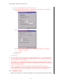
8.
Let’s look back to the schematic and consider some highlights.
8.1. The first few rows of waveforms are the external RAM interface, including control lines, address
lines, and data lines. See how RAMNWE pulses low twice during every word write to the byte
memory. See how the least significant bit of the external RAM address, XA_0, is the inverse of
CLK during read cycles.
18
Getting Started with the XSOC Project v0.93
8.2. See how the next few lines (RDY, AN[15:0], READN) present the next memory access request,
and how the external RAM address XA follows AN by one cycle.
8.3. See the new instruction (XDIN[15:0]) move into the decode stage instruction register (OP[3:0]...)
and from there to the execute stage instruction register (EXOP[3:0]...).
8.4. See how a taken branch (time 250 ns) causes the next two instructions to be annulled.
8.5. The simple program generates the natural numbers. See how we increment a register by one and
write it back into the register file (time 320 ns).
12 Building XSOC
Here is how to compile the XSOC project to an FPGA configuration bitstream xsoc.bit, using the Xilinx
Student Edition 1.5 or Foundation 1.5 tools.
12.1 Verilog version
1.
Simulate your changes first. It is possible, although rare, for an erroneous design to damage an FPGA.
2.
Choose the appropriate external constraints file to use:
XS40 Board Type
XS40-005XL v1.2, v1.3
XS40-005XL v1.4, v1.4+
XS40-010XL v1.2, v1.3
XS40-010XL v1.4, v1.4+
UCF file
xsocv-05xl-13.ucf
xsocv-05xl-14.ucf
xsocv-10xl-13.ucf
xsocv-10xl-14.ucf
(How do these files differ? The -10xl versions have looser timing constraints compared to -05xl;
and the –13 versions tie XA<15> and XA16 to unused pads, whereas the –14 versions tie
XA<15>=P28 and XA16=P16 (present on v1.4+ and apparently benign on v1.4).)
Copy that file onto your current xsoc.ucf:
C:\> cd \xsoc\xsocv
C:\xsoc\xsocv> copy xsocv-??xl-??.ucf xsocv.ucf
Caution: never build an xsocv.bit using xsocv-*-14.ucf and then load it into a pre-v1.4 XS40
board. The xsocv-*-14.ucf constrains XA16 to P16 (XCBUS16). On pre-v1.4 boards, XCBUS16 is
also driven by inverter U3C (see schematic on p.17 of XESS’ XS40-manual-v1_3.pdf). The potential
output contention could damage your XS40 board (or worse)!
3.
Launch Xilinx Foundation Project Manager and open the xsocv.pdf project in \xsoc.
4.
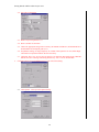
Click the Flow tab and click SYNTHESIS.
4.1. You may see this dialog.
Click yes, of course.
19
Getting Started with the XSOC Project v0.93
4.2. You will see this dialog.
4.3. Ensure Top Level specifies xsoc.
4.4. Enter a suitable version name.
4.5. Choose the appropriate Target Device Family (XC4000XL) and Device (XC4005XLPC84 or
XC4010XLPC84) and Speed grade (xl-3).
4.6. In Synthesis Settings, set target frequency to 33 MHz. Click Optimize for Area; Effort High.
Check Insert I/O pads and uncheck Preserve hierarchy.
4.7. Click Run. The Create Version process runs for a few moments. Disregard any FE-CHECK-1
and FE-CLEAN-1 warnings concerning whether any “ctrl<*> has no net attached”.
5.
Click IMPLEMENTATION to build the project. You will see this dialog:
5.1. Click Options. This opens the Options dialog.
20
Getting Started with the XSOC Project v0.93
5.1.1. User contraints should read “\xsoc\xsocv\xsocv.ucf”.
5.1.2. Click Program Options Templates>>Implementation>>Edit Template. This opens the
XC4000 Implementation Options: Default dialog.
5.1.2.1. Click the Place and Route tab.
5.1.2.2. Set Place and Route Effort Level to 5 (Best Results) and ensure “Use Timing
Constraints... is checked.
5.1.2.3. Click OK.
5.1.3. Click OK.
5.2. Click Run.
6.
The Flow Engine will run to implement your design, producing an xsocv.bit FPGA configuration
file. There will be a number of warnings about such issues as nets with no loads or no drivers, and
clock nets with non-clock connections.
7.
A few minutes later, your P&R should complete successfully, meeting timing constraints. The Flow
Engine window will automatically close and your Project Manager Console window will report Flow
Engine Completed Successfully.
8.
Spend a few minutes and review your report files, perhaps inspect the design output using
Tools>>Implementation>>EPIC Design Editor or Tools>>Implementation>>Floorplanner, and review
the static timing analysis with Tools>>Simulation/Verification>>Interactive Timing Analyzer.
12.2 Schematics version
1.
Simulate your changes first. It is possible, although rare, for an erroneous design to damage an FPGA.
21
Getting Started with the XSOC Project v0.93
2.
Choose the appropriate external constraints file to use:
XS40 Board Type
XS40-005XL v1.2, v1.3
XS40-005XL v1.4, v1.4+
XS40-010XL v1.2, v1.3
XS40-010XL v1.4, v1.4+
UCF file
xsoc-05xl-13.ucf
xsoc-05xl-14.ucf
xsoc-10xl-13.ucf
xsoc-10xl-14.ucf
(How do these files differ? The -10xl versions have looser timing constraints compared to -05xl;
and the –13 versions tie XA<15> and XA16 to unused pads whereas the –14 versions tie
XA<15>=P28 and XA16=P16 (present on v1.4+ and apparently benign on v1.4).)
Copy that file onto your current xsoc.ucf:
C:\> cd \xsoc\xsoc
C:\xsoc\xsoc> copy xsoc-??xl-??.ucf xsoc.ucf
Caution: never build an xsoc.bit using xsoc-*-14.ucf and then load it into a pre-v1.4 XS40
board. The xsoc-*-14.ucf constrains XA16 to P16 (XCBUS16). On pre-v1.4 boards, XCBUS16 is
also driven by inverter U3C (see schematic on p.17 of XESS’ XS40-manual-v1_3.pdf). The potential
output contention could damage your XS40 board (or worse)!
3.
Launch Xilinx Foundation Project Manager and open the xsoc.pdf project in \xsoc.
4.
Use File>>Project Type to set the project type appropriate to Xilinx FPGA in your XS prototyping
card.
4.1. If it’s an XS40-005XL, select XC4000XL and 4005XLPC84 and 3.
4.2. If it’s an XS40-010XL, select XC4000XL and 4010XLPC84 and 3.
4.3. The design as shipped assumes a v1.2 board with a 12 MHz clock. If your XS40 board is version
v1.3, v1.4 or v1.4+ board, you’ll need to modify the design to change from the VGA macro to the
VGA_12_5_MHZ macro; see chapter 13, Changing the Clock Frequency, thereby editing XSOC
to swap the VGA_12_5_MHZ for the VGA.
5.
Click the Flow tab and click IMPLEMENTATION to build the project. You may see this dialog:
5.1. If so, click Yes. Soon the Implement Design dialog appears:
5.2. Enter a suitable version name.
5.3. Click Options. This opens the Options dialog.
5.3.1. User contraints should read “\xsoc\xsoc\xsoc.ucf”.
22
Getting Started with the XSOC Project v0.93
5.3.2. Click Program Options Template>>Implementation>>Edit Template. This opens the
XC4000 Implementation Options: Default dialog.
5.3.2.1. Click the Place and Route tab.
5.3.2.2. Set Place and Route Effort Level to 5 (Best Results) and ensure “Use Timing
Constraints... is checked.
5.3.2.3. Click OK.
5.3.3. Click OK.
5.4. Click Run.
6.
The Flow Engine will run and build your .bit file. There will be a number of warnings about such
issues as nets with no loads or no drivers, and clock nets with non-clock connections.
7.
A few minutes later, your P&R should complete successfully, meeting timing constraints. The Flow
Engine window will automatically close and your Project Manager Console window will report Flow
Engine Completed Successfully.
8.
Spend a few minutes and review your report files, perhaps inspect the design output using
Tools>>Implementation>>EPIC Design Editor or Tools>>Implementation>>Floorplanner, and review
the static timing analysis with Tools>>Simulation/Verification>>Interactive Timing Analyzer.
13 Changing the Clock Frequency
XSOC ships with a bilevel VGA controller configured to generate VGA compatible horizontal and vertical
syncs given the XS40 v1.2’s 12 MHz clock frequency. VGA shifts pixels on each clock edge, giving a
pixel frequency of 24 MHz.
23
Getting Started with the XSOC Project v0.93
The newer v1.3 and v1.4 boards do not have a fixed 12 MHz oscillator, rather each has a programmable
oscillator that can generate frequencies of 100 MHz divided by some integer, e.g. 100 MHz, 50 MHz, 33.3
MHz, 25 MHz, 20 MHz, 16.7 MHz, 14.3 MHz, 12.5 MHz, 11.1 MHz, etc. The oscillator cannot generate a
frequency of 12 MHz, however.
Therefore the v1.2 XSOC design, as it stands, will not generate VGA compatible sync frequencies in an
XS40 v1.3. Let’s see what we have to do to modify XSOC for v1.3 and later boards to once again generate
VGA compatible syncs.
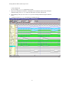
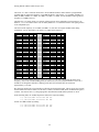
The closest clock frequency is 12.5 MHz (100 MHz ÷ 8). We take our original 12 MHz VGA timing
spreadsheet, vga.xls, and modify it to reflect a 12.5 MHz clock frequency:
12 MHZ TIMINGS
freq
cycle
hvisible
hsyncon
hsyncoff
hreset
hsynctime
linecycle
vvisible
vsyncon
vsyncoff
vreset
vsynctime
12.5 MHZ TIMINGS
1.200E+07
8.333E-08
times
2.517E-05
2.611E-05
2.988E-05
3.177E-05
3.750E-06
3.175E-05
times
1.525E-02
1.570E-02
1.576E-02
1.678E-02
6.350E-05
freq
cycle
cycles trunc
302.04
302
313.32
313
358.56
358
381.24
381
hvisible
hsyncon
hsyncoff
hreset
hsynctime
1.250E+07
8.000E-08
times
2.517E-05
2.611E-05
2.988E-05
3.177E-05
3.760E-06
3.176E-05
times
1.525E-02
1.570E-02
1.576E-02
1.678E-02
6.352E-05
linecycle
lines trunc
480.31
480
494.49
494
496.50
496
528.63
528
vvisible
vsyncon
vsyncoff
vreset
vsynctime
pix/clock
hpixels
hvisible
hbytes
vvisible
2
576
288
72
455
pix/clock
hpixels
hvisible
hbytes
vvisible
2
576
288
72
455
hpadpixels
hsyncon'
hsyncoff'
vpadlines
vsyncon'
vsyncoff'
5
308
353
12
482
484
hpadpixels
hsyncon'
hsyncoff'
vpadlines
vsyncon'
vsyncoff'
11
315
362
12
482
484
cycles trunc
314.63
314
326.38
326
373.50
373
397.13
397
lines trunc
480.31
480
494.49
494
496.50
496
528.63
528
While the horizontal blanking and sync counts (397, 288, 315, 362) have changed for the faster clock
frequency, observe the vertical blanking and sync counts (528, 455, 482, 484) are identical. This is as it
should be, for though the controller is shifting pixels faster, the horizontal line rate remains at
approximately 31.75 kHz.
We must now modify our VGA controller to reflect the new horizontal counts. This is not so easy, because
the horizontal and vertical counters are not binary counters, but rather LFSR (linear feedback shift register)
counters. We must use the lfsr design program to determine the LFSR count bit patterns we need.
In the following table, the 12 MHz bit pattern column was output by running
C:\> \xsoc\src\lfsr 10 381 288 308 353
C:\> \xsoc\src\lfsr 10 528 455 486 488
and the 12.5 MHz column by running
C:\> \xsoc\src\lfsr 10 397 288 315 362
C:\> \xsoc\src\lfsr 10 528 455 486 488
24
Getting Started with the XSOC Project v0.93
Quantity
reset horiz. counter (cycles)
horizontal. blanking (cycles)
horiz. sync on (cycles)
horiz. sync off (cycles)
reset vert. counter (lines)
vertical blanking (lines)
vertical sync on (lines)
vertical sync off (lines)
Count
(12 MHz)
381
288
308
353
528
455
486
488
Bit pattern
(12 MHz)
0x23D
0x09D
0x01A
0x10C
0x27D
0x01D
0x3F5
0x3D7
Count
(12.5 MHz)
397
288
315
362
528
455
486
488
Bit pattern
(12.5 MHz)
0x31D
0x1C4
0x122
0x3B6
0x27D
0x01D
0x3F5
0x3D7
Note in particular, the bit pattern for the count==288 in a 381-cycle 10-bit LFSR is not the same as the bit
pattern for the count==288 in a 397-cycle 10-bit LFSR.
Now we must modify the design to reflect the new (boldface) horizontal counter bit patterns.
13.1 Verilog version
As we move ahead, support for the XS40 board v1.2 is being phased out (unless we hear otherwise from
the XSOC user community). Therefore the Verilog version, in particular, the file xsocv\vga.v, is written
assuming you are using a v1.3 or v1.4/+ board with a 12.5 MHz oscillator frequency.
13.2 Schematics version
Here’s what we did to create and use a new VGA_12_5_MHZ macro.
(Note that all of this has actually been done on your behalf. The new VGA_12_5_MHZ macro has already
been added to the xsoc library, and the xsoc.sch top level schematic is now shipped with the
VGA_12_5_MHZ macro in place of the old (12 MHz) VGA macro. If you are still using a XS40 v1.2 board
with the fixed 12 MHz oscillator, you should change back to the VGA macro by applying steps 1, 8-10, and
13-14, to replace VGA_12_5_MHZ with VGA.)
1.
Start the Project Manager on the XSOC Project.
2.
Open the Project Libraries dialog (File>>Project Libraries...).
3.
Open the Library Manager.
4.
In the Libraries tab, select the xsoc library. Press ENTER to open the Objects tab.
5.
Select the VGA object and copy it (Object>>Copy...). Enter a new destination name (e.g.
VGA_12_5_MHZ) and select the same library (xsoc) to receive the new copy.
6.
Exit the Library Manager (File>>Exit).
7.
Close the Project Libraries dialog.
8.
Back in the Project Manager, open the xsoc.sch schematic.
9.
Scroll/pan to the VGA component. Select it. Replace it (Options>>Replace Symbol...) with your new
macro VGA_12_5_MHZ.
10. When the Schematic Editor replaces VGA with VGA_12_5_MHZ, it unfortunately loses the
RLOC_ORIGIN=R7C1 attribute on the object. Restore it. Double-click the object to access its Symbol
Properties. In the Parameters box, enter Name RLOC_ORIGIN and description R7C1 and click Add
and OK.
11. Enter Hierarchy mode (Hierarchy>>Hierarchy Push). Your cursor changes to an H-arrow. Doubleclick on the VGA component.
12. Scroll/pan/zoom to the H0, HBLANK, HSYNCON, HSYNCOFF area and make these changes.
12.1. Change the comment “381=23D=10_0011_1101” to “397=31D=11_0001_1101”.
25
Getting Started with the XSOC Project v0.93
12.2. Edit Bus the H0.B[9:0] label from “V,G,G,G,V,V,V,V,G,V” to “V,V,G,G,G,V,V,V,G,V”.
12.3. Change the comment “288=09D=00_1001_1101” to “288=1C4=01_1100_0100”.
12.4. Edit Bus the HBLANK.B[9:0] label from “G,G,V,G,G,V,V,V,G,V” to “G,V,V,V,G,G,G,V,G,G”.
12.5. Change the comment “308=01A=00_0001_1010” to “315=122=01_0010_0010”.
12.6. Edit Bus the HSYNCON.B[9:0] label from “G,G,G,G,G,V,V,G,V,G” to
“G,V,G,G,V,G,G,G,V,G”.
12.7. Change the comment “353=10C=01_0000_1100” to “362=3B6=11_1011_0110”.
12.8. Edit Bus the HSYNCOFF.B[9:0] label from “G,V,G,G,G,G,V,V,G,G” to
“V,V,V,G,V,V,G,V,V,G”.
13. Save your changes and exit.
14. Rebuild xsoc.
14 Project Administrivia
This section provides some general background information on the XSOC project.
14.1 Issue tracking
The XSOC Project comes with a rudimentary issues tracking system and current issues database. The
directory \xsoc\issues includes these files:
• issues-howto: explains how to format and submit an issue report.
• issues: a snapshot of known XSOC issues
• issues-list: a summary of the open, assigned, resolved, and closed known issues
• issues.awk: an awk script that produces issues-list
• n.c: the source code to reproduce issue #n
The current (beta 0.93) issues list includes:
open issues (12):
2 not-impl lcc-xr16
3 not-impl xr16asm
4 not-impl libxr16
5 not-impl libxr16
6 defect
xsoc
7 wish
libxr16
8 not-impl lcc-xr16
9 not-impl xr16asm
11 defect
xsoc
14 wish
xsoc
16 defect
doc
17 defect
xr16iss
long integers are not implemented
far branch displacements are not implemented
most kinds of mul div and mod are not implemented
variable bit-count shifts are not implemented
VGA only displays 560 pixels/line, not 576
xr16 needs a C runtime library
lcc-xr16 needs a test suite
xr16 assembler/simulator needs a test suite
timespecs do not include async RAM delay offsets
XSOC/xr16 refloorplanned for XC4010XL
xspecs.pdf: b<cond> a,-32768 broken
b<cond> a,-32768 broken
assigned issues (1):
10 not-impl xr16cpu
xr16 cpu needs a test suite
resolved issues (1):
20 defect
xsoc
problems building under Foundation 2.1i.
closed issues (6):
1 note
doc
12 wish
misc
13 defect
xsoc
15 defect
lcc-xr16
18 defect
xr16asm
19 defect
xr16asm
how to use the issues tracking system
issues tracking should include version number info
XSOC did not run on a v1.4+ board
some unsigned hex consts promoted to long
cmpi reg,-32768 broken
cmpi reg,0 broken
See the issues file for more information.
The up-to-date version of these files is at www.fpgacpu.org/xsoc/issues. Please review issues or
issues-list before reporting a new issue.
26
Getting Started with the XSOC Project v0.93
14.2 Setting proper expectations
Before diving into the XSOC project head-first, please moderate your expectations. For example:
•
A processor and system-on-a-chip is not a trivial thing. Neither is compiler development. If you are not
already an accomplished FPGA designer / compiler developer, you are encouraged to take appropriate
courses and/or work through the textbooks. For this project, I recommend that you study
Fraser and Hanson, A Retargetable C Compiler, Design and Implementation.
Van den Bout, The Practical Xilinx Designer Lab Book.
Hennessy and Patterson, Computer Organization: The Hardware/Software Interface.
•
This is unsupported experimental hardware and software. There are and will always be bugs, some
trivial, some not, some deterministic, some not, some easily fixed, some highly frustrating. The tools
(XSOC project tools and Xilinx tools) can be finicky and frustrating. Also, a great many features you
may have come to expect in a modern computing platform are not implemented.
•
Unsupported? That’s right. The company makes no representations that any issues, bugs, defects,
incomplete features, etc. will ever be addressed. It’s an “as is” kit, “what you get is what you get” and
there is no commitment that a new release will ever come.
(This is not the license agreement. See the XSOC License Agreement in the file LICENSE.)
•
If there are project updates, they will be posted to www.fpgacpu.org/xsoc and announced on
[email protected].
•
We are disinclined to answer homework questions, RTFM questions, problems better addressed to
Xilinx Tech Support, etc. We ignore anonymous email – if it is not transparently obvious from your
email return address, be sure to state your name and affiliation in your message body. And we’re
often incommunicado for a week at a time, and even then we’re probably too busy to help you much
anyway. So to whom can you turn?
14.3 Help!
You are encouraged to subscribe to [email protected], the FPGA CPU and XSOC project mailing
list, by sending an email message to [email protected]. You will receive a message
from the egroups.com Manager asking you to confirm your subscription request.
The charter of [email protected] states: “This list is for discussion of the design and
implementation of field-programmable gate array based processors and integrated systems. It is also for
discussion and community support of the XSOC Project.”
This list is archived at http://www.egroups.com/group/fpga-cpu.
Mail [email protected] to unsubscribe.
If you wish to report a bug, problem, or feature request, or other issue, please read the issues-howto
before you send your report.
14.4 How you can help
You can help improve this project by:
•
Subscribing to the mailing list, contributing to it, and helping to improve the signal/noise ratio and the
quality and relevance of the list by keeping your questions, answers, and discussions on-topic, polite,
civil, and friendly.
•
By reading issues submissions, and by volunteering to take ownership of an issue, investigate it, and/or
fix it.
•
By trying to work through this Getting Started guide, and then filling out the survey form
\xsoc\survey and returning it to [email protected]. As survey says, aggregated
answers and select written answers may occasionally be posted to [email protected].
27
Getting Started with the XSOC Project v0.93
14.5 Summary of email addresses and contact information
Email addresses:
• [email protected]: group list for discussions of FPGA processors, integrated systems, and the
XSOC project, for XSOC support questions, and for XSOC release announcements. Also (for the time
being) the place to send issues reports.
• [email protected]: for returning completed surveys (thank you).
• [email protected]: to contact Gray Research LLC for other matters pertaining to XSOC. No
support questions, please.
• [email protected]: to contact Jan Gray. No support questions, please.
Company contact information:
Jan Gray
President
Gray Research LLC
P.O. Box 6156
Bellevue, WA, 98008-1156
15 Acknowledgements
The editor is grateful for the many helpful contributions of Mike Butts, Tom Cantrell, Steve Ciarcia, Ingo
Cyliax, Robert Ferguson, Philip Freidin, Ole Moller, Michael Rutenberg, Graham Seaman, Dave Vanden
Bout, and Brian von Herzen, and for the great work of the fine folks at Circuit Cellar, XESS, and Xilinx,
and of the lcc authors, Chris Fraser and David Hanson.
16 Revision History
Version
0.6
0.91
0.92
0.93
Date
03/08/00
03/13/00
03/20/00
04/06/00
Description
More or less complete.
Fix a few Windows 95/98-isms.
Fix problems reported by MB, PF, and DC, including issue #13.
Add Verilog version and related testing and build topics.
28