1
UM0116
User manual
STR7 family Flash programming
Introduction
This reference manual describes how to program the Flash memory of an STR7
microcontroller.
The STR7 embedded Flash memory can be programmed using In-Circuit Programming or
In-Application programming.
The In-Circuit programming (ICP) method is used to update the entire contents of the
Flash memory, using the JTAG protocol to load the user application into the microcontroller.
ICP offers quick and efficient design iterations and eliminates unnecessary package
handling or socketing of devices.
In contrast to the ICP method, In-Application Programming (IAP) can use any
communication interface supported by the microcontroller (I/Os, USB, CAN, UART...) to
download the data to be programmed in memory. IAP allows you to re-program the Flash
memory while the application is executing. Nevertheless, part of the application has to have
been previously programmed in one of the Flash banks using ICP.
The MCUs supported by this reference manual are the STR71x, STR73x and STR75x.
Glossary
This section gives a brief definition of acronyms and abbreviations used in this document:
FPEC (FLASH Program/Erase controller): The write operations to the 2 banks are managed
by an embedded FPEC.
IAP (In-Application Programming): The IAP is the ability to re-program the Flash memory of
a microcontroller while the user program is running.
ICP (In-Circuit Programming): The ICP is the ability to program the Flash memory of a
microcontroller using JTAG protocol while the device is mounted on the user application
board.
JTAG (Joint Test Action Group): The debug interface of the ARM7TDMI core is based on the
Joint Test Action Group (JTAG) protocol.
September 2006
Rev 4
1/27
www.st.com
Contents
UM0116
Contents
1
Flash module organization . . . . . . . . . . . . . . . . . . . . . . . . . . . . . . . . . . . . 4
2
Read/program the STR7 embedded Flash . . . . . . . . . . . . . . . . . . . . . . . 6
2.1
Introduction . . . . . . . . . . . . . . . . . . . . . . . . . . . . . . . . . . . . . . . . . . . . . . . . 6
2.2
Read operation . . . . . . . . . . . . . . . . . . . . . . . . . . . . . . . . . . . . . . . . . . . . . . 6
2.3
Write operation . . . . . . . . . . . . . . . . . . . . . . . . . . . . . . . . . . . . . . . . . . . . . . 6
2.4
2.5
3
2/27
2.3.1
Executing the first Write operation from RAM . . . . . . . . . . . . . . . . . . . . . 6
2.3.2
Generic Write Operation Description . . . . . . . . . . . . . . . . . . . . . . . . . . . . 6
2.3.3
Erase Operation Description . . . . . . . . . . . . . . . . . . . . . . . . . . . . . . . . . . 7
2.3.4
Word Program Operation Description . . . . . . . . . . . . . . . . . . . . . . . . . . . 7
2.3.5
Double Word Program operation description . . . . . . . . . . . . . . . . . . . . . . 8
2.3.6
Suspend Operation Description . . . . . . . . . . . . . . . . . . . . . . . . . . . . . . . . 8
2.3.7
Errors during Write Operation . . . . . . . . . . . . . . . . . . . . . . . . . . . . . . . . . 9
2.3.8
Interrupted Write Operation . . . . . . . . . . . . . . . . . . . . . . . . . . . . . . . . . . . 9
2.3.9
Write Operation Summary . . . . . . . . . . . . . . . . . . . . . . . . . . . . . . . . . . . 10
Register description . . . . . . . . . . . . . . . . . . . . . . . . . . . . . . . . . . . . . . . . . 10
2.4.1
Flash Control Register 0 (FLASH_CR0) . . . . . . . . . . . . . . . . . . . . . . . . 10
2.4.2
Flash Control Register 1 (FLASH_CR1) . . . . . . . . . . . . . . . . . . . . . . . . 14
2.4.3
Flash Data Registers (FLASH_DR1-DR0) . . . . . . . . . . . . . . . . . . . . . . . 15
2.4.4
Flash Address Register (FLASH_AR) . . . . . . . . . . . . . . . . . . . . . . . . . . 16
2.4.5
Flash Error Register (FLASH_ER) . . . . . . . . . . . . . . . . . . . . . . . . . . . . . 16
Write Operation Examples . . . . . . . . . . . . . . . . . . . . . . . . . . . . . . . . . . . . 17
2.5.1
Word Program . . . . . . . . . . . . . . . . . . . . . . . . . . . . . . . . . . . . . . . . . . . . 17
2.5.2
Double Word Program . . . . . . . . . . . . . . . . . . . . . . . . . . . . . . . . . . . . . . 17
2.5.3
Sector Erase . . . . . . . . . . . . . . . . . . . . . . . . . . . . . . . . . . . . . . . . . . . . . 17
2.5.4
Suspend and Resume . . . . . . . . . . . . . . . . . . . . . . . . . . . . . . . . . . . . . . 18
2.5.5
Erase Suspend, Program and Resume . . . . . . . . . . . . . . . . . . . . . . . . . 18
Flash memory protection . . . . . . . . . . . . . . . . . . . . . . . . . . . . . . . . . . . . 19
3.1
Write protection . . . . . . . . . . . . . . . . . . . . . . . . . . . . . . . . . . . . . . . . . . . . 19
3.2
Debug/Readout protection . . . . . . . . . . . . . . . . . . . . . . . . . . . . . . . . . . . . 19
3.3
Unprotection strategy . . . . . . . . . . . . . . . . . . . . . . . . . . . . . . . . . . . . . . . . 20
3.3.1
Temporary unprotection . . . . . . . . . . . . . . . . . . . . . . . . . . . . . . . . . . . . . 20
3.3.2
Permanent unprotection . . . . . . . . . . . . . . . . . . . . . . . . . . . . . . . . . . . . . 20
UM0116
Contents
3.4
3.5
Register description . . . . . . . . . . . . . . . . . . . . . . . . . . . . . . . . . . . . . . . . . 21
3.4.1
Flash non volatile write protection register (FLASH_NVWPAR) . . . . . . 21
3.4.2
Flash NV access protection register 0 (FLASH_NVAPR0) . . . . . . . . . . 22
3.4.3
Flash NV access protection register 1 (FLASH_NVAPR1) . . . . . . . . . . 23
Protection code examples . . . . . . . . . . . . . . . . . . . . . . . . . . . . . . . . . . . . 24
4
Flash register map . . . . . . . . . . . . . . . . . . . . . . . . . . . . . . . . . . . . . . . . . 25
5
Revision history . . . . . . . . . . . . . . . . . . . . . . . . . . . . . . . . . . . . . . . . . . . 26
3/27
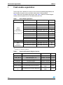
Flash module organization
1
UM0116
Flash module organization
The on-chip Flash is divided in 2 banks that can be read and modified independently one
from the other: one bank can be read while another bank is being modified.
Table 1 shows the Flash Module Organization, while Table 2 shows the Control Register
interface, with the registers that can be addressed by the CPU.
Table 1.
Flash module organization
Bank
Bank 0
256 Kbytes
Program Memory
+
8K SystemMemory4)
Sector
Addresses (Offset)
Size (bytes)
Bank 0 Flash Sector 0 (B0F0)
0x00 0000 - 0x00 1FFF
8K
Bank 0 Flash Sector 1 (B0F1)
0x00 2000 - 0x00 3FFF
8K
Bank 0 Flash Sector 2 (B0F2)
0x00 4000 - 0x00 5FFF
8K
Bank 0 Flash Sector 3 (B0F3)
0x00 6000 - 0x00 7FFF
8K
Bank 0 Flash Sector 4 (B0F4)
0x00 8000 - 0x00 FFFF
32K
Bank 0 Flash Sector 5 (B0F5)
0x01 0000 - 0x01 FFFF
64K2)
Bank 0 Flash Sector 6 (B0F6)
0x02 0000 - 0x02 FFFF
64K1)2)
Bank 0 Flash Sector 7 (B0F7)
0x03 0000 - 0x03 FFFF
64K1)2)
Bank 0 SystemMemory Sector4) 0x10 C0000 - 0x10DFFF4)
Bank 1
16 Kbytes
Data Memory3)
8K4)
Bank 1 Flash Sector 0 (B1F0)
0x0C 0000 - 0x0C 1FFF
8K
Bank 1 Flash Sector 0 (B1F1)
0x0C 2000 - 0x0C 3FFF
8K
1) Not available in 128K versions. 2) Not available in 64K versions. 3) Not available in STR73x.
4) Available only in STR73x and STR75x.
Table 2.
Control and Protection Register Interface
Name
Description
FLASH_CR1-0
Flash Control Registers 1-0
0x10 0000 - 0x10 0007 2 x 32-bit
FLASH_DR1-0
Flash Data Registers 1-0
0x10 0008 - 0x10 000F 2 x 32-bit
FLASH_AR
Flash Address Register
0x10 0010 - 0x10 0013
32-bit
FLASH_ER
Flash Error Register
0x10 0014 - 0x10 0017
32-bit
FLASH_NVWPR
Non Volatile Write Protection Register
0x10 DFB0 - 0x10
DFB3
32-bit
0x10 DFB8 - 0x10
DFBF
2 x 32-bit
FLASH_NVAPR1Non Volatile Access Protection Register 0-1
0
4/27
Addresses
Size
UM0116
Flash module organization
The Flash program memory is organized in 32-bit wide memory cells which can be used for
storing both code and data constants. The flash module is located at a specific base
address in the memory map of each STR7 Microcontroller type. For the base address,
please refer to the related STR7 Microcontroller Reference Manual.
SystemMemory is a sector used to boot the device in SystemMemory Boot Mode. The area
is reserved for use by STMicroelectronics. It is programmed by ST when the device is
manufactured and protected against spurious write/erase operations.
Bank 1 contains 16 Kbytes of Data Memory: it is divided into 2 sectors (8 Kbytes each). You
can program application data in this area.
You can Program Bank 0 and Bank 1 independently, i.e. you can read from one bank while
writing to the other.
The write operations of the two banks are managed by an embedded Flash Program/Erase
Controller (FPEC). The high voltage needed for Program/Erase operations is internally
generated.
The Flash memory can be protected against different types of unwanted access
(read/write/erase). There are two types of protection:
●
Sector Write Protection
●
Flash DEBUG/READOUT Protection
Refer to Section 3 for more details.
During a Flash write operation any attempt to read the bank under modification will output
invalid data. This means that the Flash bank is not fetchable when a write operation is
active.
Note:
The write operation commands must be executed from another bank or another memory
(internal RAM or external memory).
You can program Flash memory using In-Circuit Programming and In-Application
programming.
5/27
Read/program the STR7 embedded Flash
2
Read/program the STR7 embedded Flash
2.1
Introduction
UM0116
This section describes how to read or to program the STR7 embedded Flash.
2.2
Read operation
The embedded flash module can be addressed directly, as a common memory space. Any
32-bit data read operation accesses the content of the Flash module through dedicated read
senses and provides the requested data.
2.3
Write operation
In this section, a Flash write operation refers either to a program operation, or an erase
operation:
2.3.1
●
A program operation is a word, a double word or set protection programming operation
of the Flash module (writing ‘0’ to some bits of the selected word)
●
An erase operation is a sector erase of the Flash module (writing ‘1’ to all bits of the
selected sector).
Executing the first Write operation from RAM
After an MCU reset, the Flash module is ready and the CPU can start fetching code from it.
However, the built-in Flash Erase/Program procedures are not initialized during the MCU
reset phase, this is only done when the first Flash Erase/Program instruction is executed.
The Erase/Program procedures are stored in a reserved area of bank 0. While they are
being initialized Flash bank 0 is not accessible for the user.
The first Flash Erase/Program operation is started when the WMS bit is set. After setting
this bit, Bank 0 is no longer accessible. For this reason the code to be executed after setting
the WMS bit (Polling the bits LOCK, BSYA0 and BSYA0) must be fetched from RAM.
Also, due to this initialization, the first Erase/Program operation will take more time than
other subsequent Erase/Program operations.
2.3.2
Generic Write Operation Description
In general, each write operation is started through a sequence of 3 steps:
●
The first step selects the desired operation (Program or Erase) by setting the
corresponding selection bit in the Flash Control Register 0 (FLASH_CR0).
●
The second step defines the information needed for the write operation:
●
Address in the Flash Address Register (FLASH_AR) and data in the Flash Data
Registers (FLASH_DR0, FLASH_DR1) for program operation
●
Or sectors in Flash Control Register 1 (FLASH_CR1) for erase operation.
●
The last step starts the write operation, setting the start bit WMS in the FLASH_CR0.
Once selected, but not yet started, the operation can be canceled by resetting the operation
selection bit from Flash Control Register 0 (FLASH_CR0).
6/27
UM0116
Read/program the STR7 embedded Flash
Once the write operation is started, the Flash controller checks the validity of the operation
(see Section 2.3.7 on page 9). When validity has been verified, it sets the BSY bits in
FLASH_CR0 while processing the operation. The Flash controller releases the BSY bits
when the operation is completed.
The Flash controller can only manage one write operation at a time. For example, it is not
possible to program a word while erasing a sector even if the word belongs to a different
sector. During a write operation to a user bank, any access to the bank is forbidden and will
return undefined data.
This means that code or data fetches cannot be made while a write operation on the bank is
being performed.
To bypass this limitation, for long operations like a sector erase, a suspend mechanism
enables to temporary stop it to perform higher priority tasks. After the high priority tasks
complete, the previous operation can be completed.
The bits in the FLASH_CR0 register allow you to monitor the Flash controller status and to
check if a write operation is on going.
An interrupt request can be generated at the end of each write operation if the INTM bit in
the FLASH_CR0 register is set.
It is recommended to read the Flash Error Register (FLASH_ER), at the end of a write
operation, to check that the operation was completed successfully.
2.3.3
Erase Operation Description
An erase operation allows you to erase a sector or the full content of a bank:
●
Select the erase operation, setting the Sector Erase (SER) bit in the Flash Control
Register 0 (FLASH_CR0).
●
Select the sectors to be erased in Flash Control Register 1 (FLASH_CR1).
●
Start the erase operation, setting the start bit WMS in the FLASH_CR0.
Note:
To erase the full content of a bank, just set all the BxFy bits in Flash Control Register 1
(FLASH_CR1).
2.3.4
Word Program Operation Description
A single word program operation allows you to program a single word in the Flash module:
●
Select the single word program operation, by setting the Word Program (WPG) bit in
the Flash Control Register 0 (FLASH_CR0).
●
Write the word to be programmed in the Flash Data Register (FLASH_DR0).
●
Write the address where to program in the Flash Address Register (FLASH_AR).
●
Start the program operation, by setting the start bit WMS in the FLASH_CR0.
7/27
Read/program the STR7 embedded Flash
2.3.5
UM0116
Double Word Program operation description
A double word program operation allows you to program two words in the Flash module:
●
Select the double word program operation, by setting the Double Word Program
(DWPG) bit in the Flash Control Register 0 (FLASH_CR0).
●
Write the least significant word to be programmed in the Flash Data Register 0
(FLASH_DR0) and the most significant word to be programmed in the Flash Data
Register 1 (FLASH_DR1).
●
Write the address of the location to be programmed in the Flash Address Register
(FLASH_AR).
●
Start the program operation, setting the start bit WMS in the FLASH_CR0.
Note:
The address where the double word is to be programmed should be aligned on a double
word boundary. In case the address is not at a double word boundary, the SEQER flag of
the Flash Error Register will be set.
2.3.6
Suspend Operation Description
As described in the above Section 2.3 on page 6, the Flash controller can only manage one
write operation at a time. This might be a limitation for long operations like a sector erase:
the application may need to quickly access the bank while the operation still needs some
time to complete.
A suspend mechanism enables to suspend an on-going operation and resume it afterward:
●
Set the SUSP bit in FLASH_CR0, to suspend the operation.
●
Wait until the Flash controller acknowledges the suspend of the operation resetting
both BSY bits and the LOCK bit in the FLASH_CR0 register.
To resume the operation:
Note:
●
Clear the SUSP bit in the FLASH_CR0 register.
●
Configure FLASH_CR0 with the operation that has been suspended and needs to be
resumed.
●
Restart the write operation, by setting the start bit WMS in the FLASH_CR0.
To resume a suspended operation, only the FLASH_CR0 needs to be reconfigured with the
operation to be resumed. All data in FLASH_CR1, FLASH_DR0, FLASH_DR1 and
FLASH_AR are saved when the suspend is requested. A Resume Error (See Section 2.3.7
on page 9) will be generated when the resumed operation configured in FLASH_CR0 does
not match with the suspended operation.
Not all operations are available during suspend:
●
When in program suspend, the Flash controller accepts only the following operations:
read and program resume.
●
When in erase suspend, the Flash controller accepts only the following operations:
read, erase resume and program. Program operation can be performed in any sector
with the exception of the sectors in erase suspend.
Note:
Single/double Word Program operations cannot be suspended during erase suspend.
Note:
Erase operations are not allowed during program suspend.
8/27
UM0116
2.3.7
Read/program the STR7 embedded Flash
Errors during Write Operation
A complete set of checks is done by the Flash controller after each write operation to verify
that the operation completed successfully.
The FLASH_ER register provides dedicated flags for each error type that might arise during
a write operation as well as a global flag triggered on any error.
The following errors may occur during write operation:
●
●
2.3.8
Hardware errors:
–
Program Error: this error reports a physical failure of a Flash cell that can no more
be programmed. The word where this error occurred must be rejected.
–
Erase Error: this error reports a physical failure of a Flash cell that can no more be
programmed. The sector where this error occurred must be rejected.
Software errors:
–
1 over 0 error: this error reports an attempt to program at ‘1’ a bit, whereas it was
already programmed at ‘0’. The data should be masked with the current value, or
the sector should erased before reprogramming this data.
–
Sequence error: this error reports that an incorrect sequence has been executed
to trigger the write operation. The code applying the sequence should be checked.
–
Resume error: this error reports that a suspend write operation has not been
correctly resumed. The full operation sequence has to be redone.
–
Protection error: this error reports an attempt to write a sector which is write
protected. If the sector effectively needs to be written, the sector should first be
temporary unprotected, then the full operation sequence has to be reexecuted.
Interrupted Write Operation
A failing write operation is normally flagged in the Flash Error Register (FLASH_ER).
Nevertheless, if during a write operation, the internal 1.8V Vdd supply drops below the
internal Flash low voltage detector threshold or if a reset is triggered, the operation is
suddenly interrupted and the Flash controller is reset to Read mode without updating the
FLASH_ER.
The sectors or words that were under modification while the write operation has been
interrupted becomes undefined. The interrupted write operation must be repeated to
recover these resources.
9/27
Read/program the STR7 embedded Flash
2.3.9
UM0116
Write Operation Summary
A summary of the available Flash controller write operations is shown in Table 3
Table 3.
2.4
Flash Write Operations
Operation
Select bit
Address and Data
Start bit
Word Program
WPG
FLASH_AR + FLASH_DR0
WMS
Double Word Program
DWPG
FLASH_AR + FLASH_DR0 +
FLASH_DR1
WMS
Sector Erase
SER
FLASH_CR1
WMS
Set Protection1)
SPR
FLASH_AR + FLASH_DR0
WMS
Program/Erase Suspend
SUSP
None
None2)
1)
See Section 3 for details on memory protection.
2)
The FLASH_CR0 register needs to be reconfigured with the operation to be resumed.
Register description
In this section, the following abbreviations are used:
Table 4.
2.4.1
Abbreviations
read/write (rw)
Software can read and write to these bits.
read-only (r)
Software can only read these bits.
read/clear (rc_w0)
Software can read as well as clear this bit by writing ‘0’. Writing ‘1’ has
no effect on the bit value.
read/set (rs)
Software can read as well as set this bit. Writing ‘0’ has no effect on
the bit value.
reserved (Res.)
Reserved bit, must be kept at reset value.
Flash Control Register 0 (FLASH_CR0)
Address offset: 0x10 0000h
Reset value: 0x0000 0000h
31
30
29
28
27
26
25
24
23
22
21
20
WMS
SUSP
WPG
DWPG
SER
Res.
Res.
SPR
Res.
SMBM2)
INTM
INTP
rc_w0
rw
rc_w0
10
9
6
5
4
rs
rw
rw
rw
rw
15
14
13
12
11
PWD
3)
rw
8
7
Reserved
LOCK
rw
r
1)
Not available in STR73x.
2)
Available only in STR73x.
3)
19
18
17
16
Reserved
3
Res.
2
BSYA1
r
1)
1
0
BSYA0
Res.
r
Not available in STR75x.
The Flash Control Register 0 (FLASH_CR0) is used to enable and to monitor all the write
operations for the Flash controller.
Note:
10/27
If two or more operation selection bits (WPG, DWPG or SER) are set at the same time, they
will be ignored and the current operation will be cancelled.
UM0116
Read/program the STR7 embedded Flash
Bit 31
Bit 30
WMS: Write Mode Start.
This bit must be set to start a write operation (program or erase) in the Flash
module. At the end of the write operation or during a suspend, this bit is
automatically reset.
Resetting this bit by software has no effect.
Note:
Setting WMS if bit ERR in the FLASH_ER register is high has no
effect: the operation is ignored.
Note:
It is forbidden to start a new write operation (by setting WMS high)
with bit SUSP in the FLASH_CR0 register is high. To resume a
suspended operation, SUSP must be first cleared and then WMS
must be set again.
SUSP: Suspend (Read/Write).
This bit must be set to suspend the current single/double word program or
sector erase operation in order to read data in the same bank under
modification or to program data in another bank. The Suspend operation resets
the Flash bank to normal read mode (automatically resetting bits BSYA1,
BSYA0).
This bit must be reset by the user when the suspend request has been served.
WMS bit must be set again, together with the appropriate bit (WPG, DWPG,
SER) to resume a suspended operation.
Note:
In Program Suspend, the Flash controller accepts only the
following operations: Read and Program Resume.
When in Erase Suspend, the Flash controller accepts only the
following operations: Read, Erase Resume and Program
(single/double Word Program operations cannot be suspended
during Erase Suspend).
Note:
It is forbidden to start a new Write operation when this bit is
already set.
Bit 29
WPG: Word Program (Read/Write).
This bit must be set to select the single Word (32-bit) Program operation in the
Flash module. The single Word Program operation allows to program 0s in
place of 1s. The Flash Address to be programmed must be written in the
FLASH_AR register, while the Flash Data to be programmed must be written in
the FLASH_DR0 register before starting the execution by setting bit WMS. This
bit is automatically reset at the end of the Word Program operation.
Bit 28
DWPG: Double Word Program.
This bit must be set to select Double Word (64 bits) Program operation in the
Flash module. The Double Word Program operation allows to program 0s in
place of 1s. The Flash Address to be programmed (aligned with even words)
must be written in the FLASH_AR register, while the 2 Flash Data to be
programmed must be written in the FLASH_DR0 register (even word) and
FLASH_DR1 register (odd word) before starting the execution by setting bit
WMS. This bit is automatically reset at the end of the Double Word Program
operation.
11/27
Read/program the STR7 embedded Flash
UM0116
Bit 27
SER: Sector Erase.
This bit must be set to select the Sector Erase operation in the Flash module.
The Sector Erase operation allows erasure of all the flash locations in the
selected sector back to a value of 0xFFFFFFFF. The sectors to erase are
selected by setting bits BxFy in the FLASH_CR1 register (In the STR73x, the
SystemMemory sector is excluded from this operation). The SER bit must be
programmed before starting the execution by setting the WMS bit. It is not
necessary to pre-program the sectors to 0x00, because this is done
automatically. This bit is automatically reset at the end of the Sector Erase
operation.
Bit 26:25
Reserved, must be kept at reset value (0).
Bit 24
SPR: Set Protection.
This bit must be set to select the Set Protection operation. The Set Protection
operation allows to program 0s in place of 1s in the Flash Non Volatile
Protection Registers. After selecting the write protection operation you must
write the address of the FLASH_NVWPARx register in the FLASH_AR register
and write the protection bit data in the FLASH_DR0 register. Then set the
WMS bit to execute the operation. See Section 3.5 for an example. A sequence
error is flagged by bit SEQER of FLASH_ER if the address written in
FLASH_AR out of range. This bit is automatically reset at the end of the Set
Protection operation.
Bit 23
Reserved, must be kept at reset value (0).
Bit 22
SMBM: SystemMemory Boot Mode (Read/Clear).
This bit is set automatically by the FPEC during initialization phase if M1/M0 =
“10”.
0: User Boot mode.
1: SystemMemory Boot Mode. The SystemMemory sector is mirrored in 0x0,
allowing the Flash Reset Vector at 0x10C000 to be fetched in SystemMemory
Boot Mode. SystemMemory can be accessed both in 0x0 and in 0x10C000
while sector B0F0 is not accessible.
Note:
12/27
In STR73x, the SystemMemory code does not perform this remapping operation so this bit has to be cleared by user software
after booting from SystemMemory.
Bit 21
INTM: end of write Interrupt Mask (Read/Write).
If this bit is set, the Flash controller generates an interrupt at the end of each
Write Operation.
Bit 20
INTP: end of write Interrupt Pending (Read/Clear).
This bit is automatically set at the end of a write operation in the Flash, if bit
INTM is set. This bit has to be software reset by the interrupt service routine.
Bit 19:16
Reserved, must be kept at reset value (0).
UM0116
Read/program the STR7 embedded Flash
Bit 15
PWD: Power Down Mode (Read/Write).
When the microcontroller is put in a specific low power mode (see note below),
the Flash module can be put into two different low power modes.
0: Normal Mode (default), Flash Stand-by mode is selected (immediate read
from Flash is possible, but some residual power consumption is present).
1: The Flash module enters Power-Down mode. (recovery time of 20µs needed
before reading, but lower power consumption)
Note:
In the STR71x family the PWD bit acts only in STOP and LPWFI
modes. Whereas in the STR73x it acts only in LPWFI mode. For
further details, refer to the specific STR7 microcontroller reference
manual and datasheet, Power section.
Bit 14:5
Reserved, must be kept at reset value (0).
Bit 4
LOCK: Flash Register Access Locked (Read Only).
When this bit is set, it means that the access to all the Flash control registers is
locked: any read access to the registers will output invalid data (0xE6000010)
and any write access will be ineffective. Please note that the “1” of the invalid
data is located exactly in the position of the LOCK bit: therefore it is the only bit
the user can always access to detect the status of the Flash registers. The
LOCK bit is automatically set when the Flash bit WMS is set.
Once it is found low, the rest of FLASH_CR0 and all the other Flash registers
are user accessible.
Bit 3
Reserved, must be kept at reset value (0).
Bit 2:1
BSY[1:0]: Bank 1:0 Busy (Read Only).
These bits indicate that a write operation is ongoing in the corresponding bank.
They are automatically set when bit WMS is set. A Set Protection operation
sets bit BSY0. When these bits are set any read access to the corresponding
bank will output invalid data, while any write access to the bank will be ignored.
At the end of the write operation or during a Program or Erase Suspend these
bits are automatically reset and the bank returns to read mode. After a Program
or Erase Resume these bits are automatically set again. All BSY[1:0] bits
remain high for a maximum of 20µs after Power-Up and when exiting PowerDown mode, meaning that the Flash banks are not yet ready to be accessed.
Bit 0
Reserved, must be kept at reset value (0).
13/27
Read/program the STR7 embedded Flash
2.4.2
UM0116
Flash Control Register 1 (FLASH_CR1)
Address offset: 0x10 0004h
Reset value: 0x0000 0000h
31
30
29
28
27
26
Reserved
15
14
13
25
B1S
12
11
10
24
1)
B0S
rs
rs
9
8
23
Reserved
1)
22
21
1)
20
19
18
Reserved
17
B1F1
16
1)
B1F01)
rw
rw
7
6
5
4
3
2
1
0
B0F7
B0F6
B0F5
B0F4
B0F3
B0F2
B0F1
B0F0
rw
rw
rw
rw
rw
rw
rw
rw
Not available in STR73x.
The Flash Control Register 1 (FLASH_CR1) is used to specify the Sectors or the Banks to
be erased, or during any write operation started with the WMS bit to monitor the status of
each sector and each bank of the module.
Bit 31:26
Reserved, must be kept at reset value (0).
Bit 25:24
B1S, B0S: Bank 1-0 Status.
At the end of any Sector Erase operation these bits are automatically
modified by hardware to give the status of the 2 banks:
0: No errors detected during erase operation on bank x,
1: Error detected during the erase operation on bank x.
Bit 23:18
Reserved, must be kept at reset value (0).
Bit 17:16
B1F[1:0]: Bank 1 Flash Sector 1:0 Control/Status.
These bits must be set by the user during a Sector Erase operation to select
the sectors to be erased in bank 1. If no errors are detected these bits are
automatically cleared at the end of the Sector Erase operation. The meaning
of B1Fy bits for sector y of bank 1 is given in Table 5.
Bit 15:8
Reserved, must be kept at reset value (0).
Bit 7:0
B0F(7:0): Bank 0 Flash Sector 7:0 Control/Status.
These bits must be set by the user during a Sector Erase operation to select
the sectors to be erased in bank 0. If no errors are detected, these bits are
automatically reset at the end of the Sector Erase operation. The meaning of
B0Fy bits for sector y of Bank 0 is provided in Table 5.
Table 5.
14/27
Sectors (BxFy) Status Bits Meaning
FLASH_
ER.ERR
FLASH_
CR0.BSYx
FLASH_
CR0.SUSP
FLASH_
CR1.BxFy
FLASH_CR1.BxFy = 1 meaning
1
-
-
1
Erase Error in Sector y of Bank x
0
1
-
1
Erase operation on-going in Sector
y of Bank x
0
0
1
1
Erase Suspended in Sector y of
Bank x
0
0
0
0
Erase completed with no errors
UM0116
2.4.3
Read/program the STR7 embedded Flash
Flash Data Registers (FLASH_DR1-DR0)
Address offset (FLASH_DR1): 0x10 000Ch
Address offset (FLASH_DR0): 0x10 0008h
Reset value: 0xFFFF FFFFh
31
30
29
28
27
26
25
24
23
22
21
20
19
18
17
16
DIN31
DIN30
DIN29
DIN28
DIN27
DIN26
DIN25
DIN24
DIN23
DIN22
DIN21
DIN20
DIN19
DIN18
DIN17
DIN16
rw
rw
rw
rw
rw
rw
rw
rw
rw
rw
rw
rw
rw
rw
rw
rw
15
14
13
12
11
10
9
8
7
6
5
4
3
2
1
0
DIN15
DIN14
DIN13
DIN12
DIN11
DIN10
DIN9
DIN8
DIN7
DIN6
DIN5
DIN4
DIN3
DIN2
DIN1
DIN0
rw
rw
rw
rw
rw
rw
rw
rw
rw
rw
rw
rw
rw
rw
rw
rw
The Flash Address Register (FLASH_AR) and the Flash Data Registers (FLASH_DR1-0)
must be written by software, prior to starting a programming operation, to specify the target
address and the data to be programmed in Flash.
Bit 31:0
DIN[31:0]: Data Input 31:0 (Read/Write).
These bits must be written with the Data to be programmed in the Flash
using any of the following operations: Word Program, Double Word Program
and Set Protection.
15/27
Read/program the STR7 embedded Flash
2.4.4
UM0116
Flash Address Register (FLASH_AR)
Address offset: 0x10 0010h
Reset value: 0x0000 0000h
31
30
29
28
27
26
25
24
23
22
21
Reserved
15
14
13
12
11
10
ADD15 ADD14 ADD13 ADD12 ADD11 ADD10
rw
rw
rw
rw
rw
rw
20
19
18
17
ADD20 ADD19 ADD18 ADD17
16
ADD16
rw
rw
rw
rw
rw
9
8
7
6
5
4
3
2
1
0
ADD9
ADD8
ADD7
ADD6
ADD5
ADD4
ADD3
ADD2
rw
rw
rw
rw
rw
rw
rw
rw
Reserved
Bit 31:21
Reserved, must be kept at reset value (0).
Bit 20:2
ADD(20:2): Address 20:2 (Read/Write).
These bits must be written with the Address of the Flash location to program
in the following operations: single/double Word Program.
In Double Word Program the ADD2 bit must be 0.
Bit 1:0
2.4.5
Reserved, must be kept at reset value (0).
Flash Error Register (FLASH_ER)
Address offset: 0x10 0014h
Reset value: 0x0000 0000h
31
30
29
28
27
26
25
24
23
22
21
20
19
18
17
16
6
5
4
3
2
1
0
Res.
Res.
10ER
PGER
ERER
ERR
-
-
rc_w0
rc_w0
rc_w0
rc_w0
Reserved
15
14
13
12
Reserved
11
10
9
8
WPF
rc_w0
16/27
7
RESER SEQER
rc_w0
rc_w0
Bit 31:9
Reserved, always read as 0.
Bit 8
WPF: Write Protection Flag.
This bit is automatically set when trying to program or erase a write protected
sector. This bit has to be cleared by software.
Bit 7
RESER: Resume Error.
This bit is automatically set when a suspended Program or Erase operation is
not resumed correctly due to a protocol error. In this case, the suspended
operation is aborted. This bit has to be cleared by software.
Bit 6
SEQER: Sequence Error.
This bit is automatically set when the control registers (FLASH_CR1-0,
FLASH_AR, FLASH_DR1-0) are not correctly filled to execute a valid Write
Operation. In this case, no Write Operation is executed. This bit has to be
cleared by software.
Bit 5:4
Reserved, must be kept at reset value (0).
UM0116
Read/program the STR7 embedded Flash
Bit 3
10ER. 1 over 0 Error.
This bit is automatically set when trying to program to 1 bits previously
programmed to 0 (this does not happen when programming the Protection
bits). This error is not due to a failure of the Flash cell, but only flags that the
desired data has not been written. This bit has to be cleared by software.
Bit 2
PGER: Program Error.
This bit is automatically set when a Program error occurs during a Flash write
operation. This error is due to a real failure of a Flash cell, that can no longer
be programmed. The word where this error occurred must be discarded. This
bit has to be cleared by software.
Bit 1
ERER: Erase Error.
This bit is automatically set when an Erase error occurs during a Flash write
operation. This error is due to a real failure of a Flash cell, that can no longer
be erased. This kind of error is fatal and the sector where it occurred must be
discarded. This bit has to be cleared by software.
Bit 0
ERR: Write Error.
This bit is automatically set when an error occurs during a Flash write
operation or due to a bad write operation setup. Once the error has been
discovered and understood, ERR bit must be cleared by software.
2.5
Write Operation Examples
2.5.1
Word Program
Example: Word Program of data 0xAAAAAAAA at address 0x05554 in the Flash Module.
FLASH_CR0 |= 0x20000000; /*Set WPG in FLASH_CR0*/
FLASH_AR = 0x00005554; /*Load Add in FLASH_AR*/
FLASH_DR0 = 0xAAAAAAAA; /*Load Data in FLASH_DR0*/
FLASH_CR0 |= 0x80000000; /*Operation start*/
2.5.2
Double Word Program
Example: Double Word Program of data 0x55AA55AA at address 0x05558 and data
0xAA55AA55 at address 0x0555C in the Flash Module.
FLASH_CR0 |= 0x10000000;/*Set DWPG*/
FLASH_AR = 0x00005558;/*Load Add in
FLASH_DR0 = 0x55AA55AA; /*Load Data
FLASH_DR1 = 0xAA55AA55; /*Load Data
FLASH_CR0 |= 0x80000000; /*Operation
FLASH_AR*/
in FLASH_DR0*/
in FLASH_DR1*/
start*/
Note:
Double Word Program is always performed on the Double Word aligned on a even Word: bit
ADD2 of FLASH_AR is ignored.
2.5.3
Sector Erase
Example: Sector Erase of sectors B0F1 and B0F0 of Bank 0 in the Flash Module.
FLASH_CR0 |= 0x08000000; /*Set SER in FLASH_CR0*/
FLASH_CR1 |= 0x00000003; /*Set B0F1, B0F0*/
FLASH_CR0 |= 0x80000000; /*Operation start*/
17/27
Read/program the STR7 embedded Flash
2.5.4
UM0116
Suspend and Resume
Word Program, Double Word Program and Sector Erase operations can be suspended in
the following way:
FLASH_CR0 |=
0x40000000; /*Set SUSP in FLASH_CR0*/
Then the operation can be resumed in the following way:
FLASH_CR0 |= 0x80000000; /*Operation resume*/
Note:
Original setup of Select Operation bits in FLASH_CR0 must be restored before the
operation resume, otherwise the operation is aborted and bit RESER of FLASH_ER is set.
Note:
Before resuming a suspended erase, FLASH_CR1 must be read to check if the Erase is
already completed (FLASH_CR1=0x00000000 if Erase is completed).
2.5.5
Erase Suspend, Program and Resume
A Sector Erase operation can be suspended in order to program (Word or Double Word) in
another Sector or Bank.
Example: Sector Erase of sector B0F1 of Bank 0 in the Flash Module.
FLASH_CR0 |= 0x08000000; /*Set SER in FLASH_CR0*/
FLASH_CR1 |= 0x00000002; /*Set B0F1*/
FLASH_CR0 |= 0x80000000; /*Operation start*/
Example: Sector Erase Suspend.
FLASH_CR0 |= 0x40000000 ; /*Set SUSP in FLASH_CR0*/
while (FLASH_CR0 & 0x00000012) {}/*Loop to Wait LOCK=0 && BSY=0*/
Example: Word Program of data 0x5555AAAA at address 0x05554 in the Flash Module.
FLASH_CR0 |= 0x20000000; /*Set WPG in FLASH_CR0*/
FLASH_AR = 0x00005554; /*Load Add in FLASH_AR*/
FLASH_DR0 = 0x5555AAAA; /*Load Data in FLASH_DR0*/
FLASH_CR0 |= 0x80000000; /*Operation start*/
Once the Program operation is finished, the Erase operation can be resumed in the
following way:
FLASH_CR0 |= 0x08000000; /*Set SER in FLASH_CR0*/
FLASH_CR0 |= 0x80000000; /*Operation resume*/
Note:
18/27
Note that during the Program Operation in Erase suspend, bit SER and SUSP are low.
UM0116
3
Flash memory protection
Flash memory protection
Two kind of protections are available: sector Write protection to prevent unwanted writes and
DEBUG/READOUT Protection to avoid software piracy. They are described in the following
subsections.
The protection bits are stored in non-volatile Flash cells that are read once at reset and
stored in 3 volatile registers:
●
FLASH_NVWPAR used to store the write protection bits for each sector of the Flash
Module
●
FLASH_NVAPR1-0 used to store the DEBUG/READOUT protection bit.
The first time you program FLASH_NVWPAR or FLASH_NVAPR0 both the non-volatile and
volatile part of the register are written. At any later stage, any write to these registers will
affect only the volatile part, which will be restored with the content of the corresponding nonvolatile part at the next reset event.
The content of the non-volatile part of the register FLASH_NVAPR1 is also copied at every
reset event into the corresponding volatile register. In this case however any write will
always update both the volatile and the non-volatile parts.
Note:
Before being configured by the reset process, all the available protections are forced active
during reset.
The protection registers are not directly accessible for writing. They can be programmed
using a set protection operation and writing them as a normal write operation.
3.1
Write protection
The Flash module provides a write protection, which can be independently activated for
each sector of each bank. When a sector is Write Protected, any attempt to program or
erase will result in a Protection Error.
A flash sector can be Write Protected by programming at 0 the related bit WyPx of the
FLASH_NVWPAR register.
Note:
The Write protection operation can be executed from all the internal/external memories
including Flash Bank 0 of the Flash module.
3.2
Debug/Readout protection
If the DEBUG or READOUT bits in the FLASH_NVAPR0 are programmed at 0, the device
becomes DEBUG or READOUT protected: debug features JTAG pins and Flash
SystemMemory mode are disabled.
Note:
The Debug/Readout protection operation can be executed from all the internal/external
memories except Flash Bank 0 of the Flash module.
●
In Embedded Flash Boot Mode: the FLASH is kept enabled and the user program will
execute normally. But the debugger host can not take the control over the CPU. In
addition, if a JTAG sequence is initiated (by simply releasing the NJTRST) then the
Flash is automatically disabled and the user program execution will fail. The user has to
19/27
Flash memory protection
UM0116
ensure that the software does not provide a way for a hacker to download the Flash
memory content.
●
In Embedded SRAM Boot Mode (STR75x): the embedded Flash is automatically
disabled and thus it is not possible to download its content (it is also not possible to
execute it).
●
In Exernal Memory Boot Mode
●
–
In the STR71x, it is not possible to use EMI boot mode when DEBUG protection is
enabled.
–
In the STR75x, it is possible to use SMI boot mode when READOUT protection is
enabled, but the embedded Flash is automatically disabled and its content cannot
be downloaded or executed.
In SystemMemory Boot Mode (STR73x/STR75x), then the program executed from
SystemMemory ensures that it is not possible to output the embedded Flash memory
contents.
3.3
Unprotection strategy
3.3.1
Temporary unprotection
You can temporarily unprotect a Write protected sector, or a DEBUG/READOUT protected
Flash module.
A write protected sector can be temporarily unprotected by executing the set protection
operation and writing 1 in the associated WyPx bits of FLASH_NVWPAR. Refer to
Section 3.5 for examples. The temporary unprotection write operation can be executed from
all the internal/external memories including Flash Bank 0 of the Flash module.
The DEBUG/READOUT protected Flash module can be temporarily unprotected by
executing the set protection operation and writing 1 into this DEBUG bit but only if these
instructions are executed from the Flash Module.
To restore the write and DEBUG/READOUT protection bits, it is necessary to reset the
microcontroller or to execute a set protection operation and write ‘0’ in the corresponding
bits.
‘Temporary’ means that FLASH_NVWPAR or FLASH_NVAPR0 bits will maintain the
unprotected state until their value will be overwritten either by a reset event or through a new
set protection operation.
3.3.2
Permanent unprotection
You can permanently unprotect a DEBUG/READOUT protected Flash Module. You may
need to use this feature under certain circumstances, for example to analyze rejects.
DEBUG/READOUT protection can be disabled by programming the PDSx bits in the
FLASH_NVAPR1 register.
If the DEBUG bit is programmed to 0, disabling the protection by programming the PDSx
bits can be done only by a program executed from the Flash Module. The user software
design can ensure that this is accessible only to authorized users.
DEBUG/READOUT protection can be enabled again by programming the PENx bits in the
FLASH_NVAPR1 register. The PDSx and PENx bits can be programmed once only,
however 16 bits are provided, so you can disable and re-enable DEBUG/READOUT
20/27
UM0116
Flash memory protection
Protection up to a maximum of 16 times. PENn can be programmed to 0 only if PDSn has
been already programmed to 0. PDSn can be programmed to 0 only if PDSn-1/PENn-1 have
been already programmed to 0.
Note:
You can not permanently unprotect a write protected sector.
3.4
Register description
3.4.1
Flash non volatile write protection register (FLASH_NVWPAR)
Address offset: 0x10 DFB0h
Delivery value: 0xFFFF FFFF
31
30
29
28
27
26
25
24
23
22
21
20
19
18
17
16
W1P[1:0]1)
Reserved
rw
15
14
13
12
11
10
9
8
7
6
Reserved
5
4
3
2
1
0
W0P[7:0]
rw
1)
Not available in STR73x.
Bit 31:18
Reserved, must be kept at reset value (1).
Bit 17-16
W1P1-0: Write Protection Bank 1 sectors 1-0.
These bits, if programmed to 0, disable any writes to the sectors of bank 1.
The sectors corresponding to bits set to ‘0’ are Write protected.
Bit 15:8
Reserved, must be kept at reset value (1).
Bit 7:0
W0P(7:0): Write Protection Bank 0 sectors 7-0.
These bits, if programmed to 0, disable any writes to the respective sectors of
bank 0. The sectors corresponding to bits set to ‘0’ are Write protected.
21/27
Flash memory protection
3.4.2
UM0116
Flash NV access protection register 0 (FLASH_NVAPR0)
Address offset: 0x10 DFB8
Delivery value: 0x3569 ACFFh
31
30
29
28
27
26
25
24
23
22
21
20
19
18
6
5
4
3
2
17
16
Reserved
15
14
13
12
11
10
9
8
7
Reserved
1)
Not available in STR75x.
2)
Not available in STR71x and STR73x.
1
0
DEBUG
1)
READ
OUT2)
rw
rw
Bit 31:2
Reserved, always read as 0.
Bit 1
DEBUG: Debug Protection.
If this bit is erased to 1, protections are by-passed and the Flash is
accessible through its JTAG interface.
If DEBUG is programmed at 0 the device is DEBUG protected, the JTAG
interface is disabled.
Bit 0
Note:
In STR73x devices, when debug protection is enabled, the
SystemMemory Mode is also disabled.
Note:
If this bit is programmed to ‘0’, STMicroelectronics will not be
able to access the device to run a possible failure analysis.
READOUT: Readout Protection.
If this bit is erased to 1, protections are by-passed and the Flash is
accessible through its JTAG interface.
If READOUT is programmed at 0 the device is READOUT protected, the
JTAG interface is disabled.
Note:
22/27
If this bit is programmed to ‘0’, STMicroelectronics will not be
able to access the device to run a possible failure analysis.
UM0116
3.4.3
Flash memory protection
Flash NV access protection register 1 (FLASH_NVAPR1)
Address offset: 0x10 DFBC
Delivery value: 0xFFFF FFFF
31
30
29
28
27
26
25
24
23
22
21
20
19
18
17
16
6
5
4
3
2
1
0
PEN[15:0]
rw
15
14
13
12
11
10
9
8
7
PDS[15:0]
rw
The FLASH_NVAPR1 register is organized as 16 pairs of bits (PENx - PDSx). The delivery
value of The FLASH_NVAPR1 register is 0xFFFFFFFF. The first time you disable the
DEBUG/READOUT protection you must program to PDS0 ‘0’. To re-enable the protection
you must program to bit PEN0 ‘0’: this is possible only if PDS0 has been already
programmed to ‘0’. This cycle of disabling/re-enabling the protection can be repeated with
the next PDS1/PEN1 pair of bits and so on. PDS1 can be programmed to ‘0’ only if PEN0
has been already programmed to ‘0’, PEN1 can be programmed to ‘0’ if and only if PDS1
has been already programmed to ‘0’. The programming to ‘0’ of the bits of the
FLASH_NVAPR1 register must therefore follow the PDS0-PEN0-PDS1-PEN1-PDS2-PEN2...-PEN15 sequence, obtaining up to 16 unprotection/protection cycles.
Note:
Note:
At any reset event the non-volatile part of FLASH_NVAPR1 register is copied into its volatile
part. Unlike with the FLASH_NVAPR0 and FLASH_NVWPAR register, any write will always
update both the volatile and the non-volatile parts: i.e. no temporary unprotection is possible
with FLASH_NVAPR1 register.
Bit 31:16
PEN15-0: Protection Enable 15-0.
If bit PENx is programmed at 0 and bit PDSx+1 is erased to 1, the action of
bit DEBUG is enabled again. Bit PENx can be programmed to 0 only if bit
PDSx has been already programmed to 0.
Bit 15:0
PDS15-0: Protection Disable 15-0.
If bit PDSx is programmed at 0 and bit PENx is erased to 1, the action of bit
DEBUG is disabled (i.e. DEBUG/READOUT protection is no longer in place).
Bit PDS0 can be programmed at 0 only if bit DEBUG is already programmed
at 0. Bit PDSx can be programmed to 0 only if bit PENx-1 has already been
programmed to 0.
All the STR73x Flash protection registers (FLASH_NVWPAR, FLASH_NVAPR0 and
FLASH_NVAPR1) are write only in User boot modes and Read/Write when booting from
SystemMemory mode.
23/27
Flash memory protection
3.5
UM0116
Protection code examples
Example 1: Enable Write Protection of sectors B0F3-0 of Bank 0.
FLASH_CR0 |= 0x01000000; /*Set SPR in FLASH_CR0*/
FLASH_AR = 0x0010DFB0; /*Load Add in FLASH_AR*/
FLASH_DR0 = 0xFFFFFFF0; /*Load Data in FLASH_DR0*/
FLASH_CR0 |= 0x80000000; /*Operation start*/
Example 2: Disable Write Protection of sectors B0F3-0 of Bank 0 temporarily.
FLASH_CR0 |= 0x01000000; /*Set SPR in FLASH_CR0*/
FLASH_AR = 0x0010DFB0; /*Load Add in FLASH_AR*/
FLASH_DR0 = 0xFFFFFFFF; /*Load Data in FLASH_DR0*/
FLASH_CR0 |= 0x80000000; /*Operation start*/
Example 3: Enable Debug Protection.
FLASH_CR0 |= 0x01000000; /*Set SPR in FLASH_CR0*/
FLASH_AR = 0x0010DFB8; /*Load Add in FLASH_AR*/
FLASH_DR0 = 0xFFFFFFFD; /*Load Data in FLASH_DR0*/
FLASH_CR0 |= 0x80000000; /*Operation start*/
Example 4: Disable Debug Protection temporarily.
FLASH_CR0 |= 0x01000000; /*Set SPR in FLASH_CR0*/
FLASH_AR = 0x0010DFB8; /*Load Add in FLASH_AR*/
FLASH_DR0 = 0xFFFFFFFF; /*Load Data in FLASH_DR0*/
FLASH_CR0 |= 0x80000000; /*Operation start*/
Example 5: Disable Debug Protection permanently.
FLASH_CR0 |= 0x01000000; /*Set SPR in FLASH_CR0*/
FLASH_AR = 0x0010DFBC; /*Load Add in FLASH_AR*/
FLASH_DR0 = 0xFFFFFFFE; /*Load Data in FLASH_DR0*/
FLASH_CR0 |= 0x80000000; /*Operation start*/
Example 6: Re-Enable Debug Protection permanently, after having disabled it.
FLASH_CR0 |= 0x01000000; /*Set SPR in FLASH_CR0*/
FLASH_AR = 0x0010DFBC; /*Load Add in FLASH_AR*/
FLASH_DR0 = 0xFFFEFFFF; /*Load Data in FLASH_DR0*/
FLASH_CR0 |= 0x80000000; /*Operation start*/
Note:
24/27
You can disable and re-enable the DEBUG/READOUT Protection permanently (as shown in
examples 5 and 6) a maximum of 16 times.
UM0116
Flash register map
ADD(31:0)
0x10
0014
FLASH
_ER
0x10
DFB0
FLASH
_NVW
PAR
0x10
DFB8
FLASH
_NVAP
R0
0x10
DFBC
FLASH
_NVAP
R1
W1P0
W1P1
Reserved
B0F(7:0)
WPF
B1F0
B1F1
B1S
Reserved
Reserved
W0P(7:0)
Reserved
PEN(15:0)
Res.
FLASH
_AR
BSY0
0x10
0010
ERR
DIN(31:0)
ERER
FLASH
_DR1
DEBUG
0x10
000C
READOUT
DIN(31:0)
Reserved
Res.
FLASH
_DR0
Reserved
BSY1
0x10
0008
Reserved
Reserved
10ER
FLASH
_CR1
Reserved
PGER
0x10
0004
Res.
LOCK
FLASH
_CR0
B0S
0x10
0000
9 8 7 6 5 4 3 2 1 0
Res.
PWD
INTP
INTM
Res.
SMBM
SPR
SER
WPG
DWPG
WMS
SUSP
Addr. Regis
ter
Offset Name
Res.
Flash Register map
SEQER
Table 6.
RESER
Flash register map
31
30
29
28
27
26
25
24
23
22
21
20
19
18
17
16
15
14
13
12
11
10
4
PDS(15:0)
25/27
Revision history
5
UM0116
Revision history
Table 7.
Revision History
Date
Revision
31-Jan- 2005
1
First Issue
2
Updated introduction on page 1
Updated the Table 1 to support STR73x embedded Flash,
Added a new table (Table 2) with Control and Protection
Register Description.
Updated the register bits in line with the STR73x Flash
registers.
Added two new bits (SMBM and JBM) related to STR73x
SystemMemory Boot Mode in the FLASH_CR0 register,
Added note on page 25: All the STR73x Flash protection
registers (FLASH_NVWPAR, FLASH_NVAPR0 and
FLASH_NVAPR1) are write only.
Updated Section 4: Flash register map
Modified Address offset (0x10) in all Registers
04-Jan-2006
3
Updated Table 1 and Table 2 on page 1
Modified STR730 by STR73x
Removed the 2nd paragraph on page 5
Changed “Flash matrix“by “Flash module”
Added a note on page 6
Removed the 2nd sentence in the 1st paragraph on page 7
Removed the note on page 7
Removed the 1st paragraph on page 10
Removed the JBM bit from the FLASH_CR0 register
Updated the bit 30 description on page 12
Updated the bit 27 and bit 22 descriptions on page 13
Removed the bit 19 description on page14
Updated the bit 15 description on page 14
Updated the bit 4 description on page 14
Updated the bits 2:1 description on page 15
Updated the description of bits 20:2 on page 18
Updated the Flash write examples on pages 20 and 21
Added 2 notes on pages 22 and 23
Updated the Flash protection section
Updated the Flash register map
20-Sep-2006
4
Updated protection description for STR750 READOUT.
Add a new section Section 2.3.1 on page 6.
Changed DBGP bit name to DEBUG.
13-Jul-2005
26/27
Description of changes
UM0116
Please Read Carefully:
Information in this document is provided solely in connection with ST products. STMicroelectronics NV and its subsidiaries (“ST”) reserve the
right to make changes, corrections, modifications or improvements, to this document, and the products and services described herein at any
time, without notice.
All ST products are sold pursuant to ST’s terms and conditions of sale.
Purchasers are solely responsible for the choice, selection and use of the ST products and services described herein, and ST assumes no
liability whatsoever relating to the choice, selection or use of the ST products and services described herein.
No license, express or implied, by estoppel or otherwise, to any intellectual property rights is granted under this document. If any part of this
document refers to any third party products or services it shall not be deemed a license grant by ST for the use of such third party products
or services, or any intellectual property contained therein or considered as a warranty covering the use in any manner whatsoever of such
third party products or services or any intellectual property contained therein.
UNLESS OTHERWISE SET FORTH IN ST’S TERMS AND CONDITIONS OF SALE ST DISCLAIMS ANY EXPRESS OR IMPLIED
WARRANTY WITH RESPECT TO THE USE AND/OR SALE OF ST PRODUCTS INCLUDING WITHOUT LIMITATION IMPLIED
WARRANTIES OF MERCHANTABILITY, FITNESS FOR A PARTICULAR PURPOSE (AND THEIR EQUIVALENTS UNDER THE LAWS
OF ANY JURISDICTION), OR INFRINGEMENT OF ANY PATENT, COPYRIGHT OR OTHER INTELLECTUAL PROPERTY RIGHT.
UNLESS EXPRESSLY APPROVED IN WRITING BY AN AUTHORIZED ST REPRESENTATIVE, ST PRODUCTS ARE NOT
RECOMMENDED, AUTHORIZED OR WARRANTED FOR USE IN MILITARY, AIR CRAFT, SPACE, LIFE SAVING, OR LIFE SUSTAINING
APPLICATIONS, NOR IN PRODUCTS OR SYSTEMS WHERE FAILURE OR MALFUNCTION MAY RESULT IN PERSONAL INJURY,
DEATH, OR SEVERE PROPERTY OR ENVIRONMENTAL DAMAGE. ST PRODUCTS WHICH ARE NOT SPECIFIED AS "AUTOMOTIVE
GRADE" MAY ONLY BE USED IN AUTOMOTIVE APPLICATIONS AT USER’S OWN RISK.
Resale of ST products with provisions different from the statements and/or technical features set forth in this document shall immediately void
any warranty granted by ST for the ST product or service described herein and shall not create or extend in any manner whatsoever, any
liability of ST.
ST and the ST logo are trademarks or registered trademarks of ST in various countries.
Information in this document supersedes and replaces all information previously supplied.
The ST logo is a registered trademark of STMicroelectronics. All other names are the property of their respective owners.
© 2006 STMicroelectronics - All rights reserved
STMicroelectronics group of companies
Australia - Belgium - Brazil - Canada - China - Czech Republic - Finland - France - Germany - Hong Kong - India - Israel - Italy - Japan Malaysia - Malta - Morocco - Singapore - Spain - Sweden - Switzerland - United Kingdom - United States of America
www.st.com
27/27


![LV- リモコン[LV1-REMOCON] 取扱説明書](http://vs1.manualzilla.com/store/data/006564034_2-0c2dcdedfd4fbbec0b1c7178616c6116-150x150.png)