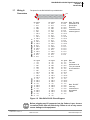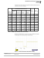
1
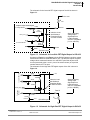
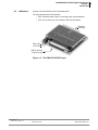
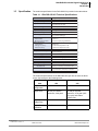
DNx-DIO-432/433 — User Manual 32-channel, Current Sink (432)/Source (433) Digital Output Layers for PowerDNA Cube and PowerDNR RACKtangle Systems Release 4.6 June 2013 PN Man-DNx-DIO-432/433-613 © Copyright 1998-2013 United Electronic Industries, Inc. All rights reserved. No part of this publication may be reproduced, stored in a retrieval system, or transmitted, in any form by any means, electronic, mechanical, by photocopying, recording, or otherwise without prior written permission. Information furnished in this manual is believed to be accurate and reliable. However, no responsibility is assumed for its use, or for any infringement of patents or other rights of third parties that may result from its use. All product names listed are trademarks or trade names of their respective companies. See the UEI website for complete terms and conditions of sale: http://www.ueidaq.com/cms/terms-and-conditions/ Contacting United Electronic Industries Mailing Address: 27 Renmar Avenue Walpole, MA 02081 U.S.A. For a list of our distributors and partners in the US and around the world, please see http://www.ueidaq.com/partners/ Support: Telephone: Fax: (508) 921-4600 (508) 668-2350 Also see the FAQs and online “Live Help” feature on our web site. Internet Support: Support: Web-Site: FTP Site: [email protected] www.ueidaq.com ftp://ftp.ueidaq.com Product Disclaimer: WARNING! DO NOT USE PRODUCTS SOLD BY UNITED ELECTRONIC INDUSTRIES, INC. AS CRITICAL COMPONENTS IN LIFE SUPPORT DEVICES OR SYSTEMS. Products sold by United Electronic Industries, Inc. are not authorized for use as critical components in life support devices or systems. A critical component is any component of a life support device or system whose failure to perform can be reasonably expected to cause the failure of the life support device or system, or to affect its safety or effectiveness. Any attempt to purchase any United Electronic Industries, Inc. product for that purpose is null and void and United Electronic Industries Inc. accepts no liability whatsoever in contract, tort, or otherwise whether or not resulting from our or our employees' negligence or failure to detect an improper purchase. Specifications in this document are subject to change without notice. Check with UEI for current status. DNA/DNR-DIO-432/433 Digital Output Layer Contents Table of Contents Chapter 1 Introduction .................................................... 1 1.1 Organization of Manual. . . . . . . . . . . . . . . . . . . . . . . . . . . . . . . . . . . . . . . . . . . . . . . . 1 1.2 The DIO-432/433 Interface Board. . . . . . . . . . . . . . . . . . . . . . . . . . . . . . . . . . . . . . . . 3 1.3 Features . . . . . . . . . . . . . . . . . . . . . . . . . . . . . . . . . . . . . . . . . . . . . . . . . . . . . . . . . . . 5 1.4 Indicators . . . . . . . . . . . . . . . . . . . . . . . . . . . . . . . . . . . . . . . . . . . . . . . . . . . . . . . . . . 6 1.5 Specification . . . . . . . . . . . . . . . . . . . . . . . . . . . . . . . . . . . . . . . . . . . . . . . . . . . . . . . . 7 1.6 Device Architecture. . . . . . . . . . . . . . . . . . . . . . . . . . . . . . . . . . . . . . . . . . . . . . . . . . . 8 1.7 Wiring & Connectors . . . . . . . . . . . . . . . . . . . . . . . . . . . . . . . . . . . . . . . . . . . . . . . . . . 9 1.8 Setting Operating Parameters . . . . . . . . . . . . . . . . . . . . . . . . . . . . . . . . . . . . . . . . . 10 1.9 Configuring the Circuit Breaker Function . . . . . . . . . . . . . . . . . . . . . . . . . . . . . . . . . 10 1.10 Configuring ADC Conversion Speed . . . . . . . . . . . . . . . . . . . . . . . . . . . . . . . . . . . . 10 Chapter 2 Programming with the High Level API . . . . . . . . . . . . . . . . . . . . . . . . . . . . . . 12 2.1 Creating a Session . . . . . . . . . . . . . . . . . . . . . . . . . . . . . . . . . . . . . . . . . . . . . . . . . . 12 2.2 Configuring the Resource String. . . . . . . . . . . . . . . . . . . . . . . . . . . . . . . . . . . . . . . . 12 2.3 Configuring for Digital I/O . . . . . . . . . . . . . . . . . . . . . . . . . . . . . . . . . . . . . . . . . . . . . 12 2.4 Configuring the Timing . . . . . . . . . . . . . . . . . . . . . . . . . . . . . . . . . . . . . . . . . . . . . . . 14 2.5 Writing Data . . . . . . . . . . . . . . . . . . . . . . . . . . . . . . . . . . . . . . . . . . . . . . . . . . . . . . . 14 2.6 Monitoring the Current . . . . . . . . . . . . . . . . . . . . . . . . . . . . . . . . . . . . . . . . . . . . . . . 15 2.7 Cleaning-up the Session. . . . . . . . . . . . . . . . . . . . . . . . . . . . . . . . . . . . . . . . . . . . . . 15 Chapter 3 Programming with the Low-level API . . . . . . . . . . . . . . . . . . . . . . . . . . . . . . . 16 Appendix A . . . . . . . . . . . . . . . . . . . . . . . . . . . . . . . . . . . . . . . . . . . . . . . . . . . . . . . . . . . . . . 17 Appendix B . . . . . . . . . . . . . . . . . . . . . . . . . . . . . . . . . . . . . . . . . . . . . . . . . . . . . . . . . . . . . . 18 Appendix C . . . . . . . . . . . . . . . . . . . . . . . . . . . . . . . . . . . . . . . . . . . . . . . . . . . . . . . . . . . . . . 20 Index . . . . . . . . . . . . . . . . . . . . . . . . . . . . . . . . . . . . . . . . . . . . . . . . . . . . . . . . . . . . . . . . . . 26 © Copyright 2013 United Electronic Industries, Inc. Tel: 508-921-4600 Date: June 2013 www.ueidaq.com Vers: 4.5 DNx-432433-ManualTOC.fm i DNA/DNR-DIO-432/433 Digital Output Layer Figures List of Figures 1-1 1-2 1-3 1-4 1-5 1-6 A-1 B-1 C-1 C-2 C-3 Schematic for Low-Side FET Digital Output in DIO-432 ............................................... 4 Schematic for High-Side FET Digital Output in DIO-433 .............................................. 4 The DNA-DIO-432/433 Layer ....................................................................................... 6 DNA/DNR-DIO-432/433 Logic Block Diagram.............................................................. 8 DNx-DIO-432/433 Pinout Diagram ............................................................................... 9 Sampling rate, CB react time, and noise .................................................................... 10 Pinout and photo of DNA-STP-62 screw terminal panel............................................. 17 Typical Soft Start Cycle............................................................................................... 18 Sync Interface Bus Diagram ....................................................................................... 20 DNA-STP-SYNC Block Diagram................................................................................. 22 Schematic of Internal Sync Connections .................................................................... 23 © Copyright 2013 United Electronic Industries, Inc. Tel: 508-921-4600 Date: June 2013 www.ueidaq.com Vers: 4.5 DNx-432433-ManualLOF.fm ii DNA/DNR-DIO-432/433 Digital Output Layer Chapter 1 Introduction Chapter 1 Introduction This document outlines the feature-set of the DNR- and DNA-DIO-432/433 layer and its use for synchronous serial-line communications applications. 1.1 Organization of Manual © Copyright 2013 United Electronic Industries, Inc. This DIO-432/433 User Manual is organized as follows: • Introduction This section provides an overview of the DIO-432 and DIO-433 interface board features, device architecture, and connectivity. • Programming with the High-Level API This chapter provides an overview of the how to create a session, configure the session, and format relevant data with the Framework API. • Programming with the Low-Level API Describes low-level API commands for configuring and using the DIO432/433 series layer for serial operating modes. • Appendix A - Accessories This appendix provides a list of accessories available for use with the DNx-DIO-432/433 serial-line communication interface board. • Appendix B - Soft Start/Stop/PWM This appendix describes the Soft Start/Soft Stop/Constant PWM feature for gradually increasing/decreasing and controlling average power applied to an output load • Appendix C - Sync Interface This appendix describes the use of the PowerDNx Sync Interface to supply a start/stop trigger to any layer in your system. • Index This is an alphabetical listing of the topics covered in this manual. Tel: 508-921-4600 Date: June 2013 www.ueidaq.com Vers: 4.5 DNx-432433-Chap1x.fm 1 DNA/DNR-DIO-432/433 Digital Output Layer Chapter 1 Introduction Manual Conventions To help you get the most out of this manual and our products, please note that we use the following conventions: Tips are designed to highlight quick ways to get the job done or to reveal good ideas you might not discover on your own. NOTE: Notes alert you to important information. CAUTION! Caution advises you of precautions to take to avoid injury, data loss, and damage to your boards or a system crash. Text formatted in bold typeface generally represents text that should be entered verbatim. For instance, it can represent a command, as in the following example: “You can instruct users how to run setup using a command such as setup.exe.” Text formatted in fixed typeface generally represents source code or other text that should be entered verbadim into the source code, initialization, or other file. Examples of Manual Conventions Before plugging any I/O connector into the Cube or RACKtangle, be sure to remove power from all field wiring. Failure to do so may cause severe damage to the equipment. Usage of Terms Throughout this manual, the term “Cube” refers to either a PowerDNA Cube product or to a PowerDNR RACKtangle rack mounted system, whichever is applicable. The term DNR is a specific reference to the RACKtangle, DNA to the PowerDNA I/O Cube, and DNx to refer to both. © Copyright 2013 United Electronic Industries, Inc. Tel: 508-921-4600 Date: June 2013 www.ueidaq.com Vers: 4.5 DNx-432433-Chap1x.fm 2 DNA/DNR-DIO-432/433 Digital Output Layer Chapter 1 Introduction 1.2 The DIO-432/ 433 Interface Board The DNx-DIO-432 and -433 32-channel digital output layers are designed for a wide variety of digital control applications. Each channel in the DIO-432 uses low-side FETs in the output circuit shown in Figure 1-1 to switch voltages in the range of 3.3 to 36VDC.The layer requires an external 3.3 to 36VDC power supply for the load. The DIO-433 uses high-side FETs in the circuit shown in Figure 1-2 and also requires an external power supply. Each channel is rated for continuous operation at 600 mA with an output voltage drop of less than 550 mV. The 32 DIO-432 outputs are configured as current sink outputs; the 32 DIO-433 outputs are configured as current source outputs. No separate clock or trigger input is provided, but the board may be controlled through the SYNC interface. Refer to “Appendix C” on page 20 for a detailed description of the SYNC interface. Both layers will not be damaged by occasional current spikes up to 2A/channel, but overall sink (432)/source(433) current should be limited to 24A per layer. Ensure that the power supply can supply enough current for the connected load. Current sense resistors mounted in the output circuits for each channel enable the board to monitor both current and voltage continuously and to detect and flag short circuits, open circuits, and other “off-normal” operating conditions for every output circuit. The monitoring feature notifies the operator and/or the host CPU via an interrupt whenever a fault occurs. This capability is a powerful diagnostic tool that enables a technician to quickly detect a fault condition and take immediate corrective action. Refer to the Framework API Reference Manual for a more detailed description of how these features can be applied. The output current monitor also provides over- and under-current protection. This feature lets you select the trip current level and also the duration of a permitted overload, which may be set as short as 10 milliseconds. When a set point is exceeded, the circuit is shut down. Each board provides 350 Vrms isolation between I/O and Cube and any other installed layers. The layers offer update rates up to 1 kHz and simplify software writes by transferring the states of all outputs as a single, 32-bit word. The DIO-432 and the -433 are fully supported by the UEIDAQ Framework API, which provides a simple and complete software interface to all popular programming languages, operating systems, and data acquisition/control application packages such as LabVIEW, DASYLab, and MATLAB. Any channel not used as a digital output may be used as a general purpose analog voltage input. For the DIO-432 (Low-Side FET), connect the voltage input signal between DOut LO (up to +40 VDC) and DGND (0 VDC), as shown in Figure 1-1. The signal level should be -0.4 to +40VDC input range relative to DGND. For the DIO-433 (High-Side FET), connect the voltage signal between DOut HI (up to -40 VDC) and GND (0 VDC), as shown in Figure 1-2. (Note that the voltage input signal range is +.4 to -40VDC relative to Vcc. NOTE: Always keep output FETs disabled when using a channel as an analog input. As a precaution, set the circuit breaker trip current to 100 µA..1mA to ensure that the measurement sensors are not damaged if a FET is accidentally turned ON. © Copyright 2013 United Electronic Industries, Inc. Tel: 508-921-4600 Date: June 2013 www.ueidaq.com Vers: 4.5 DNx-432433-Chap1x.fm 3 DNA/DNR-DIO-432/433 Digital Output Layer Chapter 1 Introduction The schematic for the low-side FET digital outputs of the 432 is shown in Figure 1-1. +Vcc user Rload Simplified Output Channel Diagram 1.5MΩ DOutLO to Voltage Monitor 30KΩ FET Transistor DOut_Low 100KΩ Inductive Load Anti-Kickback Protection Diode on Each Channel I+ to Current Monitor 0.1uF 499Ω 0.1uF 499Ω DGND Current Sense Resistor Alternate Analog Voltage Input Signal when no Load is Present and FET is disabled (-0.4 to +40VDC) I– DGND DIO-432 Layer Figure 1-1. Schematic for Low-Side FET Digital Output in DIO-432 As shown in Figure 1-1 and Figure 1-2, the DIO-432 reports a positive voltage measurement between DGND and DOUT pins. The DIO-433 reports negative voltage values measured between Vcc and DOUT pins. Both layers return current (measured at the I+ and I– pins of the sense resistor) as a positive number when the FET is open. to Current Monitor The schematic for the high-side FET digital outputs of the 433 is shown in Figure 1-2. 499 Ω I+ +Vcc 0.1 μF 0.025Ω 499 Ω I– 0.1 μF 100 KΩ Inductive Load Anti-Kickback Protection Diode on Each Channel To Voltage Monitor DOut_High FET Transistor Alternate Analog Voltage Input Signal when no Load is Present and FET is disabled (+0.4 to -40VDC) Dout Hi DOut HI 1.5 MΩ 30 KΩ Internal Rload +Vcc DIO-433 Layer Figure 1-2. Schematic for High-Side FET Digital Output in DIO-433 © Copyright 2013 United Electronic Industries, Inc. Tel: 508-921-4600 Date: June 2013 www.ueidaq.com Vers: 4.5 DNx-432433-Chap1x.fm 4 DNA/DNR-DIO-432/433 Digital Output Layer Chapter 1 Introduction 1.3 Features © Copyright 2013 United Electronic Industries, Inc. The common features of the DNx-DIO-432/433 are listed below: • 32 digital output channels: - 32 high-side channels (DNA-DIO-433 and DNR-DIO-433) - 32 low-side channels (DNA-DIO-432 and DNR-DIO-432) • Current sink outputs (DNx-DIO-432) • Current source outputs (DNx-DIO-433) • Overcurrent Protection user-programmable from 50mA to 2A and stored in EEPROM (lower on DIO-432/433-800 boards) • Overcurrent Response Time user-programmable from 10 to 5000 ms • Output Throughput Rate of 1000 samples per second (max) • 600 mA per channel of continuous output current, 2A momentary • Maximum total current 24A aggregate for all channels (per layer) • Built-in Monitoring of voltage and current on each output channel provides fault detection and simplifies system diagnostics (1% or better accuracy at ±50V input range) • Wide 3.3 V to 36 V Operating Range (requires external power supply for load) • Inductive Load Kickback Protection Diodes on every channel • Intelligent Electronic Current Monitoring (±0.5% of F.S.accuracy) on every channel with circuit breaking via FET disable • SYNC interface support — no clock/trigger input, but may be clocked/ triggered via SYNC lines • Power Consumption of the layer is 2.5W with all outputs driving 600 mA • Overcurrent and undercurrent per channel limits • Interrupt on over- or undercurrent condition • Auto-enable option is selectable per channel. It will try to restore disabled channel functionality after a programmable delay that can be up to 65 seconds long (settable in 15 nS increments) • Guaranteed output disabled (OFF) state under the following conditions: initial power-up, external power OFF, overload detected • PWM (slow-ON/slow-OFF or constant PWM) function on every output • UEI Framework Software API may be used with all popular Windows programming languages and most real time operating systems such as RT Linux, RTX, or QNX and graphical applications such as LabVIEW, MATLAB, DASYLab and any application supporting ActiveX or OPC. Tel: 508-921-4600 Date: June 2013 www.ueidaq.com Vers: 4.5 DNx-432433-Chap1x.fm 5 DNA/DNR-DIO-432/433 Digital Output Layer Chapter 1 Introduction 1.4 Indicators A photo of the DIO-432/433 unit is illustrated below. The front panel has two LED indicators: • RDY: indicates that the layer is receiving power and operational. • STS: can be set by the user using the low-level framework. DNA bus connector RDY LED STS LED DB-37 (female) 37-pin I/O connector Figure 1-3. The DNA-DIO-432/433 Layer © Copyright 2013 United Electronic Industries, Inc. Tel: 508-921-4600 Date: June 2013 www.ueidaq.com Vers: 4.5 DNx-432433-Chap1x.fm 6 DNA/DNR-DIO-432/433 Digital Output Layer Chapter 1 Introduction 1.5 Specification The technical specification for the DIO-432/433 is provided in the table below: Table 1-1. DNx-DIO-432/433 Technical Specifications Number of channels Output configuration Output port configuration Output Drive Output ON voltage Output ON impedance Output OFF impedance Output OFF leakage Overvoltage protection Overcurrent protection Current Limit Overload response time Output Monitoring Configuration 7PMUBHF"DDVSBDZ Current Accuracy Soft-Start/Stop duration Steady State PWM output Output Throughput Rate Power up / reboot state Power dissipation Isolation Operating Temp. Range 0QFSBUJOH)VNJEJUZ 7JCSBUJPOIEC 60068-2-6 IEC 60068-2-64 Shock IEC 60068-2-27 MTBF EJHJUBMPVUQVUT Current sink 4JOHMFCJUXPSE 600 mA per channel continuous; "QFBLN4NBY N7!N"JODMTUEDBCMF 0INJODMVEJOHTUEDBCMF > 1 Meg Ohm " 7%$SFWFSTFDVSSFOUNVTUCFMJNJUFEUP 1 A to prevent damage) N"" 10-5000 ms (user programmable) Multiplexed N7NBYTBNQMFEBU)[ N"NBYTBNQMFEBU)[ 4UPTFDPOET 0 to 100% in 0.4% increments. (Minimum QFSJPEJT4FD L)[NBY Off 8OPUJODMVEJOHPVUQVUTXJUDIFT 7SNT Tested -40 to +85 °C 95%, non-condensing H)[TJOVTPJEBM HSNT )[CSPBECBOESBOEPN HNTIBMGTJOFTIPDLT!PSJFOUBUJPOT HNTIBMGTJOFTIPDLT!PSJFOUBUJPOT IPVST The technical specifications for the DNx-DIO-433 layer are the same as those for the -432 except for the following items: Specificaton Item © Copyright 2013 United Electronic Industries, Inc. 432 433 Output Configuration Current Sink Current Source Output Drive 600 mA per channel continuous, 3.4A peak 600 mA per channel continuous, 2.7A peak (10% duty cycle) and 100ms duration max. Output ON Voltage Drop <550 mV at rated 600 mA <500 mV at rated 600 mA Output ON Impedance <0.9 Ohm Tel: 508-921-4600 Date: June 2013 <1.0 Ohm www.ueidaq.com Vers: 4.5 DNx-432433-Chap1x.fm 7 DNA/DNR-DIO-432/433 Digital Output Layer Chapter 1 Introduction A block diagram of a DNx-DIO-432 or -433 layer is shown below. 32-bit 66-MHz bus Control Logic A/D Converter Optical Isolation FET Transistor DOut (32) Optoisolators DC/DC MUX Sense Resistors Overvoltage Protection Device Architecture Digital I/O Connector 1.6 Figure 1-4. DNA/DNR-DIO-432/433 Logic Block Diagram As shown in Figure 1-4, layer logic is divided into isolated and non-isolated sections. The non-isolated logic complies with the full Control Logic Interface standard. The isolated side handles all functions associated with switching the output loads, sensing current and voltage, and providing over- and undercurrent and voltage monitoring and control. It also provides anti-kickback protection for inductive loads. A DC/DC module supplies 5V for controlling the FETs and powering the ADC converters. After power-up, the DC/DC is disabled. While the DC/DC is disabled, all output FETs are in disconnect mode. Current monitoring is accomplished with a 24-bit ADC that uses 0.1V as a reference voltage, increasing the dynamic range of the device. Currents up to a maximum of ±2A can be detected by the layer. If the DC/DC module is disabled, the FETs are disabled and the load is disconnected. The DIO-432 and -433 are both two-board units, comprised of a layer-specific base board (made in both DNA and DNR versions) and a plug-in layer-specific ADC board. The base boards for 432 and 433 layers use some different components, but the major difference between them is that the DIO-432 base and the DIO-433 base are fabricated in two versions, one designed for installation in a PowerDNA Cube (DNA version) and another (DNR version) designed for insertion into a RACKtangle rack enclosure. The DNA versions have a 120-pin connector for the Vertical Bus of a Cube and the DNR versions have a connector that plugs into a backplane in the rack enclosure. The DNA versions also have a jumper block for selecting a layer position within a Cube. The DNR versions do not need this feature. The ADC boards are also fabricated in two versions, one for both DNA and DNR DIO-432 and one for both DNA and DNR DIO-433 layers. The base boards contains the FETs, sensing resistors, DC/DC module, and CLI logic; the plug-in boards contain the ADCs, buffers, and associated circuits. © Copyright 2013 United Electronic Industries, Inc. Tel: 508-921-4600 Date: June 2013 www.ueidaq.com Vers: 4.5 DNx-432433-Chap1x.fm 8 DNA/DNR-DIO-432/433 Digital Output Layer Chapter 1 Introduction The pinout for the DIO-432/433 is provided below: SHIELD Pin 4 6 7 10 Signal (OE (OE %0 DO 4 (OE DO 7 DO 10 (OE %0 DO 16 (OE %0 %0 (OE %0 %0 (OE %0 %0 (OE (OE Pin Signal (OE (OE %0 %0 (OE %0 %0 (OE %0 %0 (OE %0 %0 (OE %0 %0 (OE %0 %0 (OE (OE Pin 46 48 49 51 57 58 59 60 61 Signal (OE (OE %0 DO 5 (OE DO 8 DO 11 (OE DO 14 %0 (OE %0 %0 (OE Rsvd Rsvd Rsvd SHIELD Rsvd Rsvd (OE Note: For rated performance all ground pins should be connected to the external ground. DNx-DIO-432 Pinout Wiring & Connectors Pin 4 6 7 10 Signal 7DD 7DD %0 DO 4 7DD DO 7 DO 10 7DD %0 DO 16 7DD %0 %0 7DD %0 %0 7DD %0 %0 7DD 7DD Pin Signal 7DD 7DD %0 %0 7DD %0 %0 7DD %0 %0 7DD %0 %0 7DD %0 %0 7DD %0 %0 7DD 7DD Pin 46 48 49 51 57 58 59 60 61 Signal 7DD 7DD %0 DO 5 7DD DO 8 DO 11 7DD DO 14 %0 7DD %0 %0 7DD Rsvd Rsvd Rsvd Rsvd Rsvd 7DD Note: DNx-DIO-433 Pinout 1.7 For rated performance all +Vcc pins should be connected to +Vcc. Note: Do NOT make any connections to pins marked “Rsvd”. Figure 1-5. DNx-DIO-432/433 Pinout Diagram Before plugging any I/O connector into the Cube or Layer, be sure to remove power from all field wiring. Failure to do so may cause severe damage to the equipment. © Copyright 2013 United Electronic Industries, Inc. Tel: 508-921-4600 Date: June 2013 www.ueidaq.com Vers: 4.5 DNx-432433-Chap1x.fm 9 DNA/DNR-DIO-432/433 Digital Output Layer Chapter 1 Introduction 1.8 Setting Operating Parameters For detailed instructions for configuring the layer and setting operating modes and parameters, refer to the Framework Functions DqAdv432SetAll and DqAdv432SetAll, which are described in the Framework API Reference Manual. 1.9 Configuring the Circuit Breaker Function Referring to the circuits of Figure 1-1 and Figure 1-2, the voltages from current sensing resistors are fed to 24-bit sigma-delta ADCs. The ADC outputs are then processed in the logic to perform a virtual circuit breaker function. The outputs are first compared to preset limits. If they exceed the limits, the FETs are turned OFF and the output circuit is shut down. Depending on how the channel is configured, the shutdown may either be immediate or delayed by a programmable time or by a cumulative number of detected faults. The circuit breaker function can also be configured for either User Re-enable (default) or for Auto Re-enable. The user-re-enable mode requires a write operation to re-enable output on the disabled channel. The auto-re-enable mode attempts to restore the channel after a 1 second (default) delay. If an overcurrent is detected on restart, the channel is disabled again and the re-enable attempt is repeated. The re-enable time interval is user programmable. 1.10 Configuring ADC Conversion Speed The speed and resolution of the ADC are user-programmable in the range from 0.6 to 293 Hz. Refer to the description of the function DqAdv432SetAll in the Framework API Reference Manual. The default ADC speed is 13 Hz per channel. Slower speed produces more accurate results, but increases circuit breaker disconnect time. Table 1-2 provides the ADC speeds, the time required to react to over-current and shut down the output circuit using the circuit breakers, and the accuracy. If we plot this data, we can see that accuracy is best at low sampling rates, and that the reaction time is quickest at high sampling rates. 12 4000 10 3500 8 3000 2500 6 2000 4 1500 1000 2consecutivesamples,ms Typicalnoise,mA 2 500 10 Noise [mA] CBreacttime[milliseconds] 4500 6.875 13.75 27.5 55 110 220 440 880 1760 3520 0 SamplingRate[Samples/second] Figure 1-6. Sampling rate, CB react time, and noise As a guideline, you should choose a sampling rate that is low enough to meet your accuracy need, but fast enough to allow the circuit breaker the time needed to disconnect in case of over-current. Note that the over-current limit is software configurable with the DqAdv432SetLimit function. Set sampling rate and limits to avoid over-current for a prolonged period; failing to do so may permanently damage your external equipment and/or the layer. © Copyright 2013 United Electronic Industries, Inc. Tel: 508-921-4600 Date: June 2013 www.ueidaq.com Vers: 4.5 DNx-432433-Chap1x.fm 10 DNA/DNR-DIO-432/433 Digital Output Layer Chapter 1 Introduction The table below provides sample rate, typical circuit breaker disconnect time in milliseconds, and noise in milliamps. Circuit Breaker Disconnect Time, ms Sample Rate (S/s) Immediate decision, ms 2 consecutive samples, ms 3 consecutive samples 4 consecutive samples Typical noise, mV, Vin Typical noise, mA 3520 10 20 30 41 46 10.8 1760 15 29 44 58 43 9.5 880 24 47 71 94 31 7.3 440 42 83 125 166 25 5.8 220 78 156 233 311 11 2.9 110 150 301 451 602 9.2 2.2 55 293 586 878 1171 7.1 1.7 27.5 586 1171 1757 2342 6.5 1.4 13.75 1152 2304 3456 4608 3.1 0.8 6.875 2368 4736 7104 9472 2.4 0.6 Table 1-2. Sample rate, disconnect time, and accuracy By default, the DNx-DIO-432 is configured to sample at 3520Hz and trips the circuit breaker at 2A in less than 20ms, as shown below: Figure 1-7. DIO-432 disconnect time (default setting) © Copyright 2013 United Electronic Industries, Inc. Tel: 508-921-4600 Date: June 2013 www.ueidaq.com Vers: 4.5 DNx-432433-Chap1x.fm 11 DNA/DNR-DIO-432/433 Digital Output Layer Chapter 2 Programming with the High Level API Chapter 2 Programming with the High Level API This section describes how to control the DNx-DIO-432/433 using the UeiDaq Framework High Level API. UeiDaq Framework is object oriented and its objects can be manipulated in the same manner from different development environments such as Visual C++, Visual Basic or LabVIEW. The following section focuses on the C++ API, but the concept is the same no matter what programming language you use. Please refer to the “UeiDaq Framework User Manual” for more information on use of other programming languages. 2.1 Creating a Session The Session object controls all operations on your PowerDNx device. Therefore, the first task is to create a session object: // create a session object CUeiSession session; 2.2 Configuring UeiDaq Framework uses resource strings to select which device, subsystem the Resource and channels to use within a session. The resource string syntax is similar to a web URL: String <device class>://<IP address>/<Device Id>/<Subsystem><Channel list> For PowerDNA and RACKtangle, the device class is pdna. For example, the following resource string selects digital output lines 0,1,2,3 on device 1 at IP address 192.168.100.2: “pdna://192.168.100.2/Dev1/Do0:3” 2.3 Configuring for Digital I/O The DIO-432/433 can be configured for digital output. NOTE: In Framework, a digital channel corresponds to a physical port on the device. You cannot configure a session only to access a subset of lines within a digital port. NOTE: Sessions are unidirectional. The DIO-432/433 is also unidirectional and you only need to configure one session for output. The DIO-432/433 is known as an intelligent digital output device. It can monitor the current flowing through each of its digital lines and open or close a line when the current goes above or below specified current limits. You can configure the device so that when an over or under current condition occurs, it will attempt to close the connection after a programmed delay. The device is also capable of generating a pulse train for each rising and/or falling edge, thus allowing for soft start and/or stop. © Copyright 2013 United Electronic Industries, Inc. Tel: 508-921-4600 Date: June 2013 www.ueidaq.com Vers: 4.5 DNx-432433-Chap2x.fm 12 DNA/DNR-DIO-432/433 Digital Output Layer Chapter 2 Programming with the High Level API The following call configures the digital output port of a DNx-DIO-432/433 set as device 1: // Configure session to write to port 0 on device 1 session.CreateDOProtectedChannel("pdna://192.168.100.2/Dev1/Do0", -0.01, 0.01, 200.0, false, 50.0); It configures the following parameters: • Under-current limit: when the current goes below this limit, the line opens. • Over-current limit: when the current goes above this limit, the line opens. • Current sampling rate: the rate at which the DNx-DIO-432/433 monitors current. This rate has a direct influence on how fast the DNx-DIO432/433 reacts to an under or over-current condition. • The retry status: specifies whether the DNx-DIO-432/433 attempts to close the circuit after an over or under current condition. • The retry rate: specifies how often the DNx-DIO-432/433 attempts to close the circuit. The pulse width modulation features are programmable on a per-output line basis. There are a few methods available in the CUeiDOProtectedChannel class to program the behavior of some of the output lines. First, get a pointer to the channel object: CUeiDOProtectedChannel* pChan = dynamic_cast<CUeiDOProtectedChannel *>(session.GetChanel(index)); All lines will run at the same frequency. The following code programs the pulse period to 50 us: pChan->SetPWMPeriod(50); You can configure any of the 32 output lines to generate a pulse train continuously or on a low-to-high or high-to-low transition. The following code confiigures output line 0 to generate pulses continuously and line 12 to generate pulses on low-to-high and high-to-low transitions: pChan->SetPWMMode(0, UeiDOPWMContinuous); pChan->SetPWMMode(12, UeiDOPWMSoftBoth); We must now specify the duty cycle of the lines configured in continuous mode:: pChan->SetPWMDutyCycle(0, 0.5); © Copyright 2013 United Electronic Industries, Inc. Tel: 508-921-4600 Date: June 2013 www.ueidaq.com Vers: 4.5 DNx-432433-Chap2x.fm 13 DNA/DNR-DIO-432/433 Digital Output Layer Chapter 2 Programming with the High Level API Also specify the length in us of the pulse train generated on lines configured for soft start/stop mode:: pChan->SetPWMLength(12, 1000); NOTE: When a line is configured to generate pulses continously, write operations (as described in Section 2.5 below) are ignored. The line will keep generating pulses no matter what value is written to it. A line configured for soft start will generate a pulse train after writing 1 if its previous state was 0. A line configured for soft stop will generate a pulse train after writing 0 if its previous state was 1. 2.4 Configuring the Timing You can configure the DIO-432/433 to run in simple mode (point by point) or buffered mode (ACB mode). In simple mode, the delay between samples is determined by software on the host computer. In buffered mode, the delay between samples is determined by the DNx-DIO432/433 on-board clock. The following sample shows how to configure the simple mode. Please refer to the “UeiDaq Framework User’s Manual” to learn how to use other timing modes. // configure timing for point-by-point (simple mode) session.ConfigureTimingForSimpleIO(); 2.5 Writing Data Writing data is done using a writer object. The following sample shows how to create a writer object and write data: // create a writer and link it to the session’s stream CUeiDigitalWriter writer(session.GetDataStream()); // to write a value, the buffer must contain one value per channel uInt32 data = 0xFEFE; // write one scan, the buffer must contain one value per channel writer.WriteSingleScan(&data); © Copyright 2013 United Electronic Industries, Inc. Tel: 508-921-4600 Date: June 2013 www.ueidaq.com Vers: 4.5 DNx-432433-Chap2x.fm 14 DNA/DNR-DIO-432/433 Digital Output Layer Chapter 2 Programming with the High Level API 2.6 Monitoring the Current You can monitor the current measured at each digital line. Use an Analog Input session the same way you would measure voltage from an Analog Input device. The following code shows how to measure current out of the first 4 digital lines: // create & configure session CUeiSession aiSs; aiSs.CreateAIChannel("pdna://192.168.100.2/Dev1/Ai0:3" -10.0, 10.0, UeiAIChannelInputModeDifferential); aiSs.ConfigureTimingForSimpleIO(); // create & configure reader; create buffer CUeiAnalogScaledReader aiReader(aiSs.GetDataStream()); double currents[8]; // read monitored current into buffer aiReader.ReadSingleScan(currents); 2.7 Cleaning-up the Session The session object will clean itself up when it goes out of scope or when it is destroyed. To reuse the object with a different set of channels or parameters, you can manually clean up the session as follows: // clean up the session session.CleanUp(); © Copyright 2013 United Electronic Industries, Inc. Tel: 508-921-4600 Date: June 2013 www.ueidaq.com Vers: 4.5 DNx-432433-Chap2x.fm 15 DNA/DNR-DIO-432/433 Digital Output Layer Chapter 3 Programming with the Low-level API Chapter 3 Programming with the Low-level API This chapter illustrates how to program the PowerDNA cube using the low-level API. The low-level API offers direct access to PowerDNA DAQBios protocol and also allows you to access device registers directly. However, we recommend that, when possible, you use the UeiDaq Framework High-Level API, because it is easier to use. You should need to use the low-level API only if you are using an operating system other than Windows. For additional information about low-level programming of the DIO-432/433, please refer to the PowerDNA API Reference Manual document under: Start » Programs » UEI » PowerDNA » Documentation Refer to the PowerDNA API Reference Manual on how to use the following lowlevel functions of DIO-432/433, as well as others related to cube operation: Function Description DqAdv432GetAll Gets two structures with current values and calibration data. DqAdv432SetAll Sets most of the configuration parameters. DqAdv432SetLimit DqAdv432SetPWM © Copyright 2013 United Electronic Industries, Inc. Tel: 508-921-4600 Date: June 2013 Sets the over- and under-current limits for a channel. Configures the PWM mode for a channel. www.ueidaq.com Vers: 4.5 DNx-432433-Chap3.fm 16 DNA/DNR-DIO-432/433 Digital Output Layer 17 Appendix A A. Accessories The following cables and STP boards are available for the DIO-432/433 layer. DNA-CBL-62 This is a 62-conductor round shielded cable with 62-pin male D-sub connectors on both ends. It is made with round, heavy-shielded cable; 2.5 ft (75 cm) long, weight of 9.49 ounces or 269 grams; up to 10ft (305cm) and 20ft (610cm). DNA-STP-62 The STP-62 is a Screw Terminal Panel with three 20-position terminal blocks (JT1, JT2, and JT3) plus one 3-position terminal block (J2). The dimensions of the STP-62 board are 4w x 3.8d x1.2h inch or 10.2 x 9.7 x 3 cm (with standoffs). The weight of the STP-62 board is 3.89 ounces or 110 grams. DB-62 (female) 62-pin connector: 62 61 60 59 58 57 56 55 54 53 52 51 50 49 48 47 46 45 44 43 42 41 40 39 38 37 36 35 34 33 32 31 30 29 28 27 26 25 24 23 22 UP+ UP+5 UP+5 UP+5 UP+5 UP+5 UP+5 UP+5 UP+5 UP+5 UP+5 UP+5 UP+5 UP+5 UP+5 UP+5 UP+5 UP+5 UP+5 UP+5 JT3 — 20-position terminal block: 21 20 19 18 17 16 15 14 13 12 11 10 9 8 7 6 5 4 3 2 1 UP+ UP+5 UP+5 UP+5 UP+5 UP+5 UP+5 UP+5 UP+5 UP+5 UP+5 UP+5 UP+5 UP+5 UP+5 UP+5 UP+5 UP+5 UP+5 UP+5 UP+5 UP+ UP+5 UP+5 UP+5 UP+5 UP+5 UP+5 UP+5 UP+5 UP+5 UP+5 UP+5 UP+5 UP+5 UP+5 UP+5 UP+5 UP+5 UP+5 UP+5 UP+5 44 4 47 GND JT2 — 20-position terminal block: 7 JT1 — 20-position terminal block: J2 — 5-position terminal block: 5 4 3 2 1 4)*&-% (/% SHIELD to J2 to JT1 to JT2 to JT3 J2 5 4 3 2 1 SHIELD GND 62 42 21 JT1 62-pin Connector 20 41 61 19 40 60 18 39 59 17 38 58 16 37 57 15 36 56 14 35 JT2 55 13 34 54 12 33 53 11 32 52 10 31 51 9 30 50 8 29 49 7 47 27 6 48 28 GND JT3 22 1 43 23 2 44 24 3 45 25 4 46 26 5 Figure A-1. Pinout and photo of DNA-STP-62 screw terminal panel © Copyright 2013 United Electronic Industries, Inc. Tel: 508-921-4600 Date: June 2013 www.ueidaq.com Vers: 4.5 DNx-432433-AppxA.fm DNA/DNR-DIO-432/433 Digital Output Layer 18 Appendix B Soft Start/Soft Stop/Constant PWM Feature Description B.1 Soft Start The DNx-DIO-432 and 433 layers offer a per-channel configured PWM start/ stop mode. The graphic shown in Figure A-1 shows a trace of a typical soft-start of the output (rising edge) done in 16 PWM period steps with the period set to approximately 6mS. This feature is useful in preventing premature burnout of devices such as incandescent bulbs caused by too rapid heating on startup. Note that the on/off duty cycle (ratio of on time to off time during a PWM period) varies smoothly from minimum to maximum during the start-up time. The rate at which the duty cycle increases is determined by a software parameter. For detailed instructions on setting parameters for normal/soft start/soft stop/ constant PWM operation, refer to the function DqAdv432SetPWM in the Framework API Reference Manual. PWM Period Soft Start Time Figure B-1. Typical Soft Start Cycle B.2 Soft Stop © Copyright 2013 United Electronic Industries, Inc. The DIO-432/433 can also be configured for soft stop mode of operation, which is the reverse of a soft start operation. The PWM duty cycle decreases gradually from maximum to minimum over the Soft Stop Time. The typical application for soft stop mode is a soft start operation that is implemented with inverted logic. Tel: 508-921-4600 Date: June 2013 www.ueidaq.com Vers: 4.5 DNx-432433-AppxB.fm DNA/DNR-DIO-432/433 Digital Output Layer 19 B.3 PWM Mode The constant PWM mode of operation has a constant duty cycle in which the ratio of on time to off time is fixed for the entire period of operation. The ratio value may be set as a software parameter. A typical application for this feature is a dimmer for an incandescent indicator light in which the average voltage applied to a bulb is increased or decreased by varying the PWM duty cycle. B.4 Example – Soft The code below is excerpted from Sample 432_433.c found in the DAQLib_Samples folder: Start Code // The following is an example of code for implementing the // soft start feature for: D=W/T (16PWM) #define IOM_IPADDR0 "192.168.100.2" #define DEVN 0 #define CHANNELS DQ_DIO432_CHAN #define OVERCURRENTLIMIT (1.000) // over current limit (0...2A) #define UNDERCURRENTLIMIT (-0.01) // under current limit (-2A...0) #define PWM_MODE 1 // 1-enable/0-disable PWM mode (Optional mode) #define PWM_MODE_DUTY_CYCLE 8). // Valid Duty cycle is set // with 8-bit accuracy when PWM_MODE is enabled. This value // sets the PWM duty cycle. For details, see NOTES 2 and 3 below. // In soft start/soft stop mode, (DQDIO432_PWM_SOFTSTART, // DQDIO432_PWM_SOFTSTOP,and DQDIO432_PWM_SOFTBOTH define the // number of PWM periods. For example, if <duty_cycle == 16> // output will produce 16 PWM periods upon changing output from // 1/16 duty cycle to 16/16 (or 100%)) NOTE: 1. To avoid confusion in setting up a PWM operating mode, note that the DNxDIO-432 output circuit has a FET to ground on each output. Therefore, an ON state would be a signal LOW. Conversely, the DNx-DIO-433 has a FET to +Vcc on each output. Therefore, an ON state for the 433 would be a signal HIGH. 2. To attain 0% duty cycle with a DIO-432, set the PWM_MODE for the channel to DQDIO432_PWM_DISABLED and set the corresponding output to 0 using the DqAdv40xWrite() function. For the DIO-433, a DUTY_CYCLE_LENGTH of 0 corresponds to 255/256% (99.6%) and 255 to 0%. 3. It is not possible to directly set duty cycle to 100% on a DIO-433. To attain 100% duty cycle with a DIO-433, set the PWM_MODE for the channel to DQDIO432_PWM_DISABLED and set the corresponding output to 1 using the DqAdv40xWrite() function © Copyright 2013 United Electronic Industries, Inc. Tel: 508-921-4600 Date: June 2013 www.ueidaq.com Vers: 4.5 DNx-432433-AppxB.fm DNA/DNR-DIO-432/433 Digital Output Layer 20 Appendix C PowerDNA Sync Interface C.1 Introduction The PowerDNA Sync Interface provides two capabilities that are key components of many applications. • It allows a PowerDNA Cube to be triggered by, or synchronized to, an external event or signal. • It allows the various I/O layers/boards within a cube to be triggered by and/or synchronized to, a variety of signals within the cube or to external signals brought in directly to an I/O layer. PowerDNA synchronization is based on two fixed-direction signal connections (Sync In and Sync Out) which are available on the CPU layer of the Cube as well as on four bidirectional sync signals (Sync0 through Sync3) provided on the primary internal data bus of the Cube and shared by all I/O layers as well as the CPU layer. A block diagram of the system is shown in Figure C-1. Figure C-1. Sync Interface Bus Diagram Note that the 601 Counter/Timer layer is a unique case. The counter timer capabilities of the board make it ideal for generating various timing and synchronization signals. Therefore, it is given more extensive access to the sync bus than standard layers. © Copyright 2013 United Electronic Industries, Inc. Tel: 508-921-4600 Date: June 2013 www.ueidaq.com Vers: 4.5 DNx-432433-AppxC.fm DNA/DNR-DIO-432/433 Digital Output Layer 21 FPGA bases of the various layers, combined with the Cube firmware, can be configured to create an almost unlimited set of trigger and synchronization scenarios. Not all of these are supported in the standard released product. However, our standard trigger/synchronization model can satisfy the requirements of virtually all users. The two-signal external Sync interface and the four-signal internal sync configuration are described in the two following sections, respectively. C.2 External Sync/Trigger interface Each PowerPC PowerDNA Cube provides an external Sync connector on the front panel (below the reset button, above the first I/O layer). Each DNR-12-1G module mounted in a RACKtangle rack enclosure has a sync connector on its front panel next to the reset button. These Sync interface signals may be monitored or controlled by the logic on the processor board of the Cube, or they may be connected directly to internal Sync signals shared by the internal I/O layer boards. The remainder of this section describes the external Sync interface. Please refer to Section 1.3 for details on the Cube internal sync bus. The external Sync interface provides four connections. The Sync interface pins share a common ground, but are fully isolated from the Cube itself. • Sync In • Sync Out • +5 VDC (up to 10 mA) • Ground Sync In is a dedicated input and may be used as a trigger source for the layer or to provide an external clock source to the cube. As a trigger, it supports the following modes. • Trigger Mode – Start an application on a rising or falling edge (software selectable) • Trigger/Stop Mode – Start an application on a rising (or falling) edge, Stop the application on the next rising (or falling) edge. • Gate High Mode – Run the application while Sync In is High, Stop when Sync In is Low • Gate Low Mode – Run the application while Sync In is Low, Stop when Sync In is High • Direct Layer Mode – The Sync In terminal does not have a direct “Cube wide” function, but is connected directly to a Sync pin on one of the I/O Layers. Sync Out is a dedicated output that may be configured to output any of the following: © Copyright 2013 United Electronic Industries, Inc. • Sync Buffer Mode – The Sync Out signal is simply a buffered version of Sync In • Ext Clock Mode – The internal clock of the cube is brought out to the Sync out connection and may be used to synchronize clocks across cubes or throughout an application. • Direct Layer Mode – The Sync Out signal is controlled by one of the I/O layers within the Cube. Tel: 508-921-4600 Date: June 2013 www.ueidaq.com Vers: 4.5 DNx-432433-AppxC.fm DNA/DNR-DIO-432/433 Digital Output Layer 22 There are two Sync cables available, the DNA-CBL-SYNC-RJ and the DNACBL-SYNC-30. The DNA-CBL-SYNC-RJ provides a Sync connector on one end and an RJ-45 connector on the other. This cable is used to connect external signals to the cube. Typically, the DNA-CBL-SYNC-RJ is plugged into the cube and also into the DNA-STP-SYNC panel. The DNA-STP-SYNC provides three sets of connections as shown below. • The board provides a screw terminal connection for each of the four Sync signals. • The board provides 6 parallel RJ-45 connectors. All four SYNC signals are connected in parallel as well. These parallel connections allow the user to easily connect the identical external trigger signals to multiple cubes. • The board provides a seventh RJ-45 connector with its Sync Out pin connected to the Sync In terminals of the four parallel connectors. This will allow the Sync output of a single Cube to control other Cube Sync inputs without injecting the additive delays of multiple daisy-chained DNA-CBL-SYNC-30 connections. A block diagram of the DNA-STP-SYNC is shown in Figure C-2. The DNA-CBL-SYNC-30 cable is a 30-inch cable that simply crosses the Sync In and Sync Out connections. This connects the Sync Out of one Cube to the Sync In of the next, allowing the second cube to be slaved to the first. To Master Cube Sync Out Sync In Connections to Parallel Slaved Cubes Buffers Sync Out Sync Out Sync Out Sync Out Sync Out Sync Out Sync In Sync In Sync In Sync In Sync In Sync In S1* RJ-45 Sync In RJ-45 RJ-45 RJ-45 RJ-45 RJ-45 RJ-45 BNC 6 7 GND GND +5 VDC Screw Terminals 8 9 10 BNC IN 5 BNC OUT 4 +5 VDC 3 GND * If a sync connector is plugged into the master cube connection, S1 automatically connects the Master’s Sync Out to the slave buffers 2 GND 1 BNC Sync In Sync Out Sync Out EXTERNAL Trigger / Sync If no connector is plugged into the master connector, S1 connects the Sync In BNC signal to the slave buffers Figure C-2. DNA-STP-SYNC Block Diagram © Copyright 2013 United Electronic Industries, Inc. Tel: 508-921-4600 Date: June 2013 www.ueidaq.com Vers: 4.5 DNx-432433-AppxC.fm DNA/DNR-DIO-432/433 Digital Output Layer 23 C.3 Internal Sync Connections Four Sync signals on the internal I/O interconnect bus are brought to each layer. These four lines are designated as “Sync0” through “Sync3”. The diagram below shows the configuration of the four internal Sync signals and also the pinout on the I/O layers.. Figure C-3. Schematic of Internal Sync Connections As you can see, each line is pulled up with 10k resistor. In the maximum PPC-8 cube, the total resistance is 1430 Ohms with a termination current of 2.3mA. These parameters prevent synchronization lines from bouncing and also ensure that proper drive is available from every layer. The four synchronization lines have identical functionality and any of the synchronization signals can be routed to any one of the synchronization lines. These capabilities allow great flexibility of synchronization interface configuration. However, they make the synchronization model very complex. To simplify the synchronization interface model, UEI has standardized on the following conventions. • Sync0 – dedicated trigger input • Sync1 – dedicated input clock or system timebase clock • Sync2 – inter-layer triggering • Sync3 – inter-layer clocking This line assignment addresses virtually all anticipated synchronization requirements. The logic on the CPU board allows either of the external Sync connections provided at the external Sync connector to be mapped to any of these four internal sync signals. In most applications, the master Sync input from the CPU board is connected either to the Sync0 or Sync1 terminals. If an I/O layer is being used as a master system trigger, however, it is expected that the external Sync Out connection would be mapped to either Sync2 or Sync3. © Copyright 2013 United Electronic Industries, Inc. Tel: 508-921-4600 Date: June 2013 www.ueidaq.com Vers: 4.5 DNx-432433-AppxC.fm DNA/DNR-DIO-432/433 Digital Output Layer 24 C.4 Layer Triggering & Clocking A layer can be triggered using the following sources: • Firmware executing DaqBIOS Start command • EXT0 line • Sync0 line • Sync2 line A layer can be clocked using the following sources: • Internally • EXT1 line (or EXT0 in a single-line layer) • Sync1 line • Sync3 line A layer can feed its trigger signal to Sync2 line. A layer can feed its clock signal to the Sync3 line. The Sync-Out line on the CPU layer can either output Sync[0..3] line or be used for alarm notification. C.5 Use Application Cases Use Case 1 – Starting/Stopping Multiple Layers at the Same Time (No External Trigger) This is a very common operation in ACB and DMap modes, in which the software issues a command to begin or end an application, but multiple layers within the cube need to be synchronized. If the layers involved are in software triggering mode, the firmware proceeds as follows: • The start sequence for all layers involved is stored (performed by prog_...() functions in the device driver) • All I/O layer timestamp counters are reset and synchronized with the timestamp counter on the CPU layer (this is required to align data relative to timestamps) • The start sequence is executed (normally it is a single write to LCR register of each layer involved) Layers can be clocked internally or externally in this case. Use Case 2 – External Trigger (via Sync Connector) An external trigger drives Sync-In. Sync-In is sampled by the CPU layer, which then drives the internal Sync0 line. Installed I/O layers use the Sync0 line as a trigger. Use Case 3 – External Trigger (through an I/O Layer) An I/O layer can be used to trigger one or more of the other layers in the cube. This trigger may be based directly upon an external trigger, or based upon its own trigger or terminal count. In this case, the master layer (which provides the sync signal) drives the Sync2 line. Other layers are triggered by this Sync2 signal. Clock configuration defines what signal (software, internal, external, sync bus) will be used as a layer clock.1 © Copyright 2013 United Electronic Industries, Inc. Tel: 508-921-4600 Date: June 2013 www.ueidaq.com Vers: 4.5 DNx-432433-AppxC.fm DNA/DNR-DIO-432/433 Digital Output Layer 25 Use Case 4 – External Clock An external clock can be either fed into the Sync-In input on the CPU layer or the CPU-layer PLL output may be routed to SYNC-Out and then back to SYNC-In. The clock configuration defines what signal (software, internal, external, sync bus) will be used as a layer clock. Use Case 5 – Master-Slave Clocking In this case, one layer produces a clock signal and places it on the Sync3 line. Other layer(s) in the cube then use it as their clock. The clock source can be a standard (analog/digital) layer as well as a counter-timer (CT) layer. Use Case 6 – Synchronous Buffered Input and Output In this case, an analog output layer feeds its clock to the Sync3 line. An analog input layer then uses this clock signal to synchronize its A/D sampling to the D/A layer’s clock. This allows the PowerDNA to be used in stimulus/ response applications. Use Case 7 – Sequenced Acquisition (based on the DNA-CT-601 Counter/ Timer Layer) Sequenced acquisition can be accomplished by feeding the Sync-In trigger or clock signal into one of the counter-timers on CT-601 layers (via Sync0 and Sync1 lines) and then back out to other I/O layers (using Sync2 and Sync3 lines). This allows the PowerDNA Cube to acquire data, or output waveforms, based on a predefined sequence in the CT-601 FIFO. 1. Note that this changes the definition of DQ_LN_CxCKSRCx bits. The bit combinations used are: 0 - software, 1 - internal, 2 - external, and 3 - sync interface. © Copyright 2013 United Electronic Industries, Inc. Tel: 508-921-4600 Date: June 2013 www.ueidaq.com Vers: 4.5 DNx-432433-AppxC.fm DNA/DNR-DIO-432/433 Digital Output Layer 26 Index A L ADC Conversion Speed 10 Analog Voltage Input 3 Low-level API B Block diagram 8 Organization 1 Overcurrent Response Time 5 C P Cable(s) 17 Cleaning-up the Session 15 Configuring the Circuit Breaker 10 Configuring the Resource String 12 Conventions 2 Creating a Session 12 Current Monitoring 8 Current Sense Resistors 3 Physical Description PWM Mode 19 O D DNA-STP-SYNC Block Diagram 22 E 8 S Schematic for High-Side FET 4 Schematic for Low-Side FET 4 Screw Terminal Panels 17 Setting Operating Parameters 6 Soft Stop 18 Support ii T Technical Specifications for the DIO-433 7 Example Code for Soft Start 19 H High Level API 16 W Wiring 9 12 © Copyright © 2013 Copyright 2013 United Electronic United Electronic Industries,Industries, Inc. Inc. Tel: 508-921-4600 Date: June 2013 www.ueidaq.com Vers: 4.5 DNx-432433-ManualIX.fm