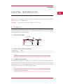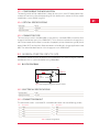
1
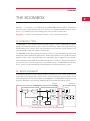
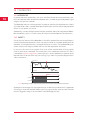
BOOMBOX USER MANUAL Contact Note imperix SA While every effort has been made to ensure accuracy in this publication, no responsibility can be accepted for errors or omissions. Data may change, as well as legislation, and the reader is strongly advised to obtain copies of the most recently issued regulations, standards, and guidelines. This publication is not intended to form the basis of a contract. Rue de l’Industrie 17 1950 Sion phone: +41 (0)27 552 06 60 fax: +41 (0)27 552 06 69 www.imperix.ch [email protected] Limited warranty Limited warranty Warranty limitation and exclusion imperix SA (hereafter “imperix”) warrants to the original purchaser or ultimate customer (hereafter “Customer”) of the present product (hereafter “Product”) that if any part proves to be defective in material or workmanship within two (2) years, such defective part will be repaired or replaced, free of charge, at imperix’s discretion, if shipped prepaid to imperix, Rue de l’Industrie 17, CH-1950 Sion, in a pack�age equal to or in the original container. The Product will be returned freight prepaid and repaired or replaced if it is determined by imperix that the part failed due to defective materials or workmanship. Otherwise, the fees will be charged to the Customer. The repair or replacement of any defective part shall be imperix’s sole and exclusive responsibility and liability under this limited warranty. imperix will have no further obligation under this limited warranty. All warranty obligations of imperix are void, in particular, but not limited to, if: The Customer must contact imperix’s customer support team and obtain a Return Authorization Number prior to shipping any Product to imperix. The relevant contact information can be found online on the imperix website (www.imperix.ch). The present warranty is the only warranty applicable to the Product. Other warranties, express or implied, including, but not limited to, the implied warranties of merchantability or fitness for a particular purpose are hereby disclaimed. If the Product is returned for repair more than 24 months after purchase, the Customer is responsible for the cost of repair. imperix will assess the repair and submit a quote to the Customer. Limitation of liability Return policy The following fees will apply when the Customer returns any Product for credit: A full credit, less a 15% fee will be issued if the product is in perfect working condition and returned within 1 month following the shipping date. If repairs are required on the returned product, their cost will be deducted from the credit. • The Product has been subject to abuse, misuse, negligence or accident; • Repairs or changes have been done to the Product by any other person than by imperix or an authorized technician; • The original Product identification (trademark, serial number) markings have been defaced, altered, or removed; • The Customer fails to perform any of the duties set forth in this limited warranty or if the Product has not been operated in accordance with instructions. Disclaimer of unstated warranties It is agreed that imperix’s liability, whether in contract, in tort, under any warranty, in negligence or otherwise shall not exceed the purchase price payed by the Customer for the said Product and under no circumstances shall imperix be liable for special, indirect, or consequential damages. No action, regardless of form, arising out of the transactions under this warranty may be brought by the purchaser more than one year after the occurrence of the cause of actions. Foreword The legacy from several decades of experience in academic teaching and research at EPFL has given the BoomBox a strong influence that makes this control platform rather different from most existing rapid prototyping systems. The present BoomBox control platform reuses some of the key features of its academic predecessor, but goes much further by providing improved flexibility, I/O capability, simplicity and reliability. Hence, the BoomBox is not only an advanced control platform, but is also, from a software point of view, a strongly layered, yet essentially open system that customers are welcome to self-appropriate and edit up to their own needs, while guaranteeing a safe and sound implementation. As a result, the BoomBox is the ultimate solution for its users to get actively involved in the control design of innovative power electronic systems, and to allow multiple developers to collaborate. Thanks to the same will to provide customers with the maximum possible flexibility and openness, numerous advanced features are already available in hardware and will be enabled in future software releases. By doing so, the flexibility of the BoomBox will be even greater, allowing to temporarily or permanently enhance its feature set within minutes depending on the varying needs. Table of Contents THE BOOMBOX 9 DIGITAL INTERFACES 1.1 INTRODUCTION 9 1.2 BLOCK DIAGRAM 9 3.1 INTERLOCK 3.1.1 Block diagram 3.1.2 Electrical specifications 3.1.3 Connector pinout 3.1.4 Usage example 19 19 19 19 20 3.2 OPTICAL PWM OUTPUTS 3.2.1 Block diagram 3.2.2 Safety 3.2.3 Configuring the modulation 3.2.4 Optical specifications 3.2.5 Connector type 20 20 20 21 21 21 3.3 GENERAL-PURPOSE INPUTS (GPI) 3.3.1 Block diagram 3.3.2 Electrical specifications 3.3.3 Connector pinout 21 21 21 21 3.4 GENERAL-PURPOSE OUTPUTS (GPO) 3.4.1 Block diagram 3.4.2 Electrical specifications 3.4.3 Connector pinout 22 22 22 22 3.5 CONTROLLER AREA NETWORK (CAN) 3.5.1 Electrical specifications 3.5.2 Block diagram 3.5.3 Connector pinout 22 22 23 23 3.6 ETHERNET 23 3.7 FRONT PANEL USB 23 1.3 CAPABILITIES 1.3.1 Interfaces 1.3.2 Safety 10 10 10 1.4 CONTROLS AND CONNECTORS 1.4.1 Front panel 1.4.2 Back panel 11 11 11 ANALOG INTERFACES 13 2.1 FEATURES AND CAPABILITIES 13 2.2 ANALOG INPUTS 13 2.2.1 Basic principle of operation 13 2.2.2 Block diagram 14 2.2.3 Electrical specifications 14 2.2.4 Configurable input impedance 14 2.2.5 Configurable gain 14 2.2.6 Configurable low-pass filter 15 2.2.7 Configurable safety limits 15 2.2.8 Saving and restoring front-end configurations15 2.2.9 Getting ADC measurements 16 2.2.10 ModuLink connector pinout and cable 16 2.2.11 Usage example 16 2.2.12 Absolute maximum ratings 16 2.3 ANALOG OUTPUTS 2.3.1 Block diagram 2.3.2 Electrical specifications 2.3.3 Setting the output voltage 17 17 17 17 19 PROGRAMMING, DEBUGGING AND MONITORING INTERFACES25 4.1 DSP JTAG 25 4.2 BACK PANEL USB CONSOLE 25 4.3 MONITORING 4.3.1 Front and back panel indicators 4.3.2 DAC interface 4.3.3 Datalogging using a USB key 4.3.4 Web interface 25 25 26 26 26 SOFTWARE ARCHITECTURE AND OPERATING SYSTEM 27 5.1 SOFTWARE ARCHITECTURE 5.1.1 Driver Layer 5.1.2 Core Layer 5.1.3 User Layer 27 27 28 28 5.2 BASIC PRINCIPLES OF OPERATION 5.2.1 Safety mechanisms 5.2.2 Interrupts and sampled operation 28 30 31 PERIPHERAL DRIVERS 33 6.1 ANALOG DATA ACQUISITION SYSTEM (ADC) 33 6.1.1 Typical workflow 33 6.1.2 Configuring the data acquisition system 34 6.1.3 Retrieving converted measurements in real time 34 6.2 PULSE-WIDTH MODULATION SYSTEM (PWM)35 6.2.1 Basic principle of operation 35 6.2.2 Generated PWM patterns 36 6.2.3 Interrupt clocks 38 6.2.4 Synchronization of frequency generators 39 6.2.5 Typical workflow 39 6.2.6 Configuring the frequency generators 40 6.2.7 Configuring the PWM channels 40 6.2.8 Activating the PWM channel 41 6.2.9 Updating the duty-cycle 41 6.2.10 Updating the configuration inside the FPGA 41 6.2.11 Enabling the outputs 41 6.3 INTERRUPT SOURCE SELECTION (IRQ) 6.3.1 Basic principle of operation 6.3.2 Registering interrupts 42 42 42 6.4 SAMPLING CLOCK 43 6.5 GENERAL-PURPOSE INPUTS (GPI) 43 6.6 GENERAL-PURPOSE OUTPUTS (GPO) 44 6.7 DIGITAL TO ANALOG CONVERTER (DAC) 44 6.8 USER LED 44 Chapter 1 THE BOOMBOX 9 Abstract — This chapter is an introduction to the BoomBox control platform. It provides a basic overview of the capabilities of the instrument. It is recommended to read this chapter first, as it introduces the terminology used in the rest of this document. Keywords — Control scheme, Regulator, Interfaces, Safety, Versatility, Modularity 1.1 INTRODUCTION The BoomBox is a new kind of modular control platform, which is tailored for the development of power electronic systems in R&D environments. When compared to existing Rapid Prototyping Systems (RPS), the presented system features similar flexibility, but superior performance and usability at lower cost. The BoomBox clearly distinguishes itself by its extensive signal conditioning, specifically tailored for power electronic applications. When compared to most general-purpose control systems, faster implementation time and better signal integrity are guaranteed. With a complete set of 100% tested software libraries, a sturdy 19” rackmount enclosure and several years of experience spent in the hands of users, the BoomBox control platform is surely the ultimate tool for the development of power electronic systems. 1.2 BLOCK DIAGRAM In the block diagram of a typical control scheme, the only parts that are left up to the user to develop are the application-specific circuit and the accompanying regulation. All the other components of the control loop are embedded in the BoomBox, helping the user to quickly develop a safe working prototype of the intended application circuit. Application BoomBox Digital Analog Switches Regulat. Modulat. Wires User Ref. ADC Data log. LPF Prog. Sensors V A Limits Fig. 1. Block diagram of the control scheme using the BoomBox. Introduction 1.3 CAPABILITIES 1.3.1 INTERFACES In power electronic applications, the users are often forced to create application-specific interfaces between the control and power parts in order to guarantee proper signal integrity and galvanic isolation. The BoomBox relies on two key concepts in order to speed up the development without any trade-off on safety : isolated fiber optic PWM outputs and versatile analog frontends that fit in with almost any sensor. Additionally, a variety of digital communication interfaces allow the integration of BoomBox-controlled systems in a wide variety of industrial and development environments. 1.3.2 SAFETY One of the key features of the BoomBox is the ability to block the entire application in case of inappropriate operation, which may be caused by an improper behavior of the controller, an unexpected event, a damaged device, etc. In such a way, the BoomBox guarantees the physical integrity of both the user and the application at all times. In any case, the user can set specific limits that will be used to block all firing signals when an overvalue is detected. The crucial point in this protection mechanism is that it is completely software-independent, meaning that it is always operational, whatever faulty behavior the DSP or the FPGA may start having. Fig. 2 shows a typical oscillogram of this safety mechanism : High limit Measurement 10 Low limit FAULT PWMH PWML Fig. 2. Operating principle of the fault detection mechanism and the protective measures. Whenever a value larger than the upper limit (or smaller than the lower limit) is detected, a fault flag is raised and latched, blocking all firing signals to their inactive state. The error remains flagged as long as the user doesn’t acknowledge the fault. The BoomBox 1.4 CONTROLS AND CONNECTORS ETHERNET RU IN N H FA IB. UL T MA SL STE A R ER VE R. G: Y: R: 1.4.1 FRONT PANEL CONFIG. & STATUS USB CORE SYNC MODULINK™ INPUTS D0 USER ••••••••••• BoomBox A0 A1 A2 3 4 5 6 D2 D3 D4 D5 D6 D7 H H H H H H H L L L L L L L L A3 0/8 1 2 D1 H 1/9 2/10 3/11 4/12 5/13 6/14 7/15 7 8 Fig. 3. Front panel view of the BoomBox. The front panel is composed of the following elements : 1) 2) 3) 4) 5) ) ) ) Ethernet port USB type B device port Rotary and push button LCD screen System and user LEDs SMA analog outputs ModuLink analog inputs Digital fiber-optic PWM outputs 1.4.2 BACK PANEL ON / OFF 110-230VAC / 50-60 Hz DIGITAL IN Optocoupled (max. 25V) DIGITAL OUT 5V logic (max. 15mA) INTERLOCK EXT. FAULT GND 1 2 3 4 5 JTAG CAN CONSOLE K LIN T. AC CAN EXT. INTERFACE 5V INTERLOCK 6 7 8 9 10 11 12 Fig. 4. Back panel view of the BoomBox. The back panel is composed of the following elements : 1) AC mains switch 2) AC mains socket (IEC 60320 C14) 3) Fan outlets 4) Isolated general-purpose inputs connector 5) Isolated general-purpose outputs connector ) External fault LED ) Interlock connector ) JTAG debugging interface ) USB type A console port 1) Console communication status LEDs 11) External interface connectors 12) CAN connectors Controls and Connectors 11 12 The BoomBox Chapter 2 ANALOG INTERFACES 13 Abstract — This chapter describes in detail the hardware aspects related to the various analog interfaces of the BoomBox. Keywords — Analog input, Analog output, Safety limits, Low-pass filter, Analog stage, Analog gain, Front-panel configuration 2.1 FEATURES AND CAPABILITIES Here are the analog interfaces of the BoomBox, along with their capabilities : » 16 analog inputs featuring : »» Selectable differential high impedance or single-ended low impedance providing compatibility with a broad range of industrial sensors. »» Programmable analog gain ensuring an optimal use of the ADC full scale. »» Programmable low-pass filter »» Programmable software-independent high and low safety limits »» 200 kHz analog bandwidth, 150 kHz maximum sampling frequency »» ModuLink connectivity »» Standard low-cost shielded connector and cabling for best noise immunity »» Power supply for sensors » 4 analog outputs featuring : »» 200 kHz analog bandwidth »» Real-time monitoring and debugging 2.2 ANALOG INPUTS 2.2.1 BASIC PRINCIPLE OF OPERATION The equivalent schematic of the complete data acquisition chain is depicted in Fig. 5. All channels are stricly identical. Each channel consists of two parts : » A hardware part, which contains the input resistor, a programmable-gain amplifier (PGA), a low-pass filter (LPF) and the analog-to-digital converter (ADC). » A software part, implemented in the DSP, that transforms the digitally-converted measurement into a meaningful quantity that can be easily manipulated : voltage in Volts, temperature in Celcius, pressure in Pascals, etc.). This transformation is done by the driver layer. The present chapter deals with the hardware part and explains how to configure the analog input chain. More information on how to properly use the software part is given in section “6.1 Analog data acquisition system (ADC)”, page 33. Features and capabilities 2.2.2 BLOCK DIAGRAM + Lim. High 14 IIN min -50 mA max +50 mA UIN min -10 V 100 Ω max +10 V Lim. Low 3 kΩ Overvalue + - A PGA LPF UADC min -10 V max +10 V e anc ped im low D UCONV cy freq float_in min -3.4e38 max +3.4e38 t uen gain f=ax+b min -32768 max +32767 gainoffse Fig. 5. Block diagram of each of the analog inputs. 2.2.3 ELECTRICAL SPECIFICATIONS Input impedance 100 Ω or 3 kΩ (user-configurable) Low-pass filter none or Ffilt = [500 Hz .. 50 kHz] (user-configurable) Sampling frequency 0 Hz .. 150 kHz (user-configurable) Resolution 16 bits Measurement range ± 1.25 V , ± 2.5 V , ± 5 V ,± 10 V (user-configurable) Safety Independent limits for each channel that trigger emergency shut-down. User-configurable comparison level VL+ ,VL- = [-10.0 V .. 10.0 V] Sensor power supply ± 15 V, 100 mA 2.2.4 CONFIGURABLE INPUT IMPEDANCE Two input configurations are available. A 3 kΩ differential input or a single-ended 100 Ω input. The latter is typically intended to be used with current output sensors, such as LEMs. Each input can be individually configured from the “Analog inputs” menu in the front panel user interface. By choosing “Low impedance : YES”, a 100 Ω resistor is switched across the input and the negative input is grounded. 2.2.5 CONFIGURABLE GAIN For each channel, the hardware gain should be defined such that the voltage UADC fully exploits the input voltage range of the analog-to-digital converter. It is defined by the relation : UADC = gain · UIN Where UIN is : » The voltage provided by the sensor if its output stage behaves as a voltage source. » UIN = 100 · IIN if the output stage of the sensor behaves as a current source. In this case, IIN is the current provided by the sensor. The possible hardware gains are shown in Table 1 : Gain in the pass-band 1 V/V 2 V/V 4 V/V 8 V/V Table 1. Possible hardware gains that can be programmed in the PGA stage of each analog input. Analog interfaces 2.2.6 CONFIGURABLE LOW-PASS FILTER A fifth-order programmable filter can be activated on each analog input channel. The cutoff frequencies of this filter can be set individually and independently for each input channel. A given frequency is considered to be in the stop band if it is larger than 8 times the selected cut-off frequency. The frequency response of the low-pass filter is given in Fig. 6. Gain [db] 80 db f [Hz] fc 8 fc Fig. 6. Frequency response of the low-pass filter. The cut-off frequencies can be freely adjusted among the values given in Table 2 : 0.5 kHz 1 kHz 1.6 kHz 2.5 kHz 4 kHz 6.4 kHz 8 kHz 10 kHz 16 kHz 20 kHz 32 kHz 40 kHz Table 2. Possible cut-off frequencies that can be programmed in the LPF stage of each analog input. 2.2.7 CONFIGURABLE SAFETY LIMITS The user can define two safety limits for each input channel : a high and a low one. If any of these limits is exceeded while the application is running, a hardware fault flag is triggered, leading to the blocking of the entire application. In order to configure this protective feature, two parameters must be configured for each input channel : » Limit high defines the highest allowed value for UADC » Limit low defines the lowest allowed value for UADC These values can be freely set from -10.0 V to 10.0 V, by steps of 100 mV. The comparison voltage is the output of the programmable gain. This means the configuration of the PGA must be taken into account when setting the safety limits. When a given limit is met or exceeded, the orange LED of the corresponding channel lights up and the CORE LED on the front panel turns red. The user can then access the fault list by selecting the “List hardware faults” option in the “Faults” menu of the front panel user interface. The fault can be acknowledged by selecting the “Acknowledge input faults” option. Caution Before acknowledging the fault, make sure that the application has returned to a safe state. 2.2.8 SAVING AND RESTORING FRONT-END CONFIGURATIONS This feature is coming soon. Analog inputs 15 2.2.9 GETTING ADC MEASUREMENTS 16 Getting ADC measurements is only a matter of calling the correct function from the DSP code. More information on the usage of the Application Programming Interface (API) can be found in section “6.1 Analog data acquisition system (ADC)”, page 33. 2.2.10 MODULINK CONNECTOR PINOUT AND CABLE The ModuLink connector is a standard low-cost 8P8C (8 position 8 contact) shielded modular connector (RJ45). The recommended cabling to be used with this connector is cat. 5E 8-conductor twisted pair shielded cable. The following table gives the pin/pair assignment definition of the ModuLink standard. The color standard used for the wiring pattern is the same as the one defined by the widespread industry standard T568B. Pin Pair Wire Color Description 1 2 1 orange stripe +15 V 2 2 2 orange solid +15 V 3 3 1 green stripe 0V 4 1 2 blue solid Positive input / current input 5 1 1 blue stripe Negative input / ground 6 3 2 green solid 0V 7 4 1 brown stripe -15 V 8 4 2 brown solid -15 V Table 3. ModuLink pin/pair assignments (right to left when facing BoomBox front panel). 2.2.11 USAGE EXAMPLE The ± 15 V supplied through the ModuLink connector enables the BoomBox to power sensors such as LEM sensors up to a maximum continuous current of 100 mA. ModuLink +15 V IMES min -25A max +25A LEM IIN LA-25P min -25 mA max +25 mA 100 Ω UIN min -2.5 V max +2.5 V -15 V Fig. 7. Block diagram of the connection of a LEM LA-25P current sensor to a ModuLink analog input. 2.2.12 ABSOLUTE MAXIMUM RATINGS 3 kΩ differential input Max. input common-mode voltage ± 10 V Max. input differential voltage ± 10 V p-p 100 Ω single-ended input Max. input current 50 mA RMS ± 15 V sensor supply Max. output current 100 mA (short-circuit protected) Analog interfaces 2.3 ANALOG OUTPUTS The four analog outputs available on the front panel (SMA connectors) provide a tool for real-time monitoring and debugging from the DSP application code. 17 Note: In order to directly connect the analog outputs to an oscilloscope, an SMA-to-BNC adapter is usually required. Reference 744-1249-ND by Digikey is a possible option. 2.3.1 BLOCK DIAGRAM float_out min -5.0 max +5.0 f D UCONV min 0 max +65535 A UOUT min -5 V max +5 V Fig. 8. Block diagram of each of the analog outputs. 2.3.2 ELECTRICAL SPECIFICATIONS Output impedance 37 Ω Update frequency 0 Hz .. 100 kHz (user-configurable) Resolution 16 bits Output range ±5V 2.3.3 SETTING THE OUTPUT VOLTAGE Setting the output voltage is only a matter of calling the correct function from the DSP. The output voltage is then updated in real-time. More information on the usage of the API can be found in section “6.7 Digital to analog converter (DAC)”, page 44. Analog outputs 18 Analog interfaces Chapter 3 DIGITAL INTERFACES 19 Abstract — This chapter describes in detail the hardware aspects related to the various digital interfaces of the BoomBox. Keywords — Interlock, Fiber-optic, Optical, PWM, GPI, GPO, CAN 3.1 INTERLOCK The interlock functionality provides the most basic safety protection, in the form of a life signal. Whenever this signal is not present at the BoomBox input, the fault flag is triggered and the application is safely stopped. 3.1.1 BLOCK DIAGRAM IIN min 0 mA max +12 mA FAULT UINTLCK min 0 V max +25 V 2.2 kΩ Fig. 9. Block diagram of the interlock input circuit. 3.1.2 ELECTRICAL SPECIFICATIONS Input impedance 2.2 kΩ High logic level range 5 V .. 25 V Warning : The reference potential for the isolated ground is shared with the general-purpose outputs. 3.1.3 CONNECTOR PINOUT The connector used for the interlock line is a 3 position 3.5 mm pin pitch connector from the Weidmüller Omnimate SL-SMT series. An interlock bypass connector is included with the BoomBox, but any application specific circuit can be combined with the interlock functionality to provide an additional layer of safety. Note : Any compatible female mating connector can be used, such as Weidmüller nb. 1615680000, available by Digikey 281-1055-ND. Interlock The pinout of the connector must be as shown in Table 4 : 20 Pin Description 1 0V 2 Interlock input 3 5V Table 4. Interlock pin assignments (left to right when facing BoomBox back panel). 3.1.4 USAGE EXAMPLE The interlock input of the BoomBox can be typically used to connect an emergency stop button, as suggested in Fig. 10 : Interlock 5V STOP IN Fig. 10. Block diagram of the connection of a normally-closed emergency switch to the interlock line. 3.2 OPTICAL PWM OUTPUTS The optical pulse-width modulated (PWM) outputs, along with their modulators implemented in FPGA, are used to drive the gates of the power switches in the user’s application circuit. 3.2.1 BLOCK DIAGRAM High and low outputs of a PWM pair FREQ GEN d perio ACTIVE ENABLEOUT FAULT PWM MOD ion ulat mod meters a r pa Fig. 11. Block diagram of each pair of fiber-optic PWM outputs. 3.2.2 SAFETY A number of conditions must be met for a valid modulation to be present at the output of the optical transceiver : » The channel must be activated by the user code. » The core of the BoomBox must be in OPERATING state, enabling the outputs. » No fault must be present. More information on the BoomBox core and the safety mechanisms can be found in section “Software architecture and operating system”, page 27. Digital interfaces 3.2.3 CONFIGURING THE MODULATION The configuration of the modulation is done by the user in the DSP code. More information on how to use the corresponding API can be found in section “6.2 Pulse-width modulation system (PWM)”, page 35. 3.2.4 OPTICAL SPECIFICATIONS Wavelength 650 nm Logic type Active high Temporal resolution 33.3 ns 3.2.5 CONNECTOR TYPE The transceiver used in the BoomBox is the industry-standard HFBR transceiver from Avago (manufacturer part num. HFBR-1528Z). This transceiver includes the Avago Versatile Link connector for the fiber. Instructions to properly crimp the correct type of plastic optical fiber (POF) to the plastic fiber connector can be found in Avago application note 1035. The recommended receiver is the Avago part num. HFBR-2528Z. 3.3 GENERAL-PURPOSE INPUTS (GPI) The general-purpose inputs enable the user to combine any external digital hardware component with a system controlled using a BoomBox. 3.3.1 BLOCK DIAGRAM x8 0 mA IIN min max +12 mA GPI[0..7] UGPI min 0 V max +25 V 2.2 kΩ Fig. 12. Block diagram of general-purpose inputs. 3.3.2 ELECTRICAL SPECIFICATIONS Input impedance 2.2 kΩ High logic level range 5 V .. 25 V 3.3.3 CONNECTOR PINOUT The connector used is a standard DE-9 shielded connector with the following pinout : Pin Description Pin Description 1 GPI0 6 GPI5 2 GPI1 7 GPI6 3 GPI2 8 GPI7 4 GPI3 9 0V 5 GPI4 Table 5. GPI pin assignments. General-purpose inputs (GPI) 21 3.4 GENERAL-PURPOSE OUTPUTS (GPO) The general-purpose outputs enable the user to combine any external digital hardware component with a system controlled using a BoomBox. 22 Note : These outputs are intended to control low-speed peripherals and are not suited for modulation output purposes. 3.4.1 BLOCK DIAGRAM x8 GPO[0..7] UGPO min 0 V max +5 V Fig. 13. Block diagram of general-purpose outputs. 3.4.2 ELECTRICAL SPECIFICATIONS High logic level 5V Max. output current 15 mA 3.4.3 CONNECTOR PINOUT The connector used is a standard DE-9 connector with the following pinout : Pin Description Pin Description 1 GPO0 6 GPO5 2 GPO1 7 GPO6 3 GPO2 8 GPO7 4 GPO3 9 0V 5 GPO4 Table 6. GPO pin assignments. 3.5 CONTROLLER AREA NETWORK (CAN) The Controller Area Network (CAN) interfaces located at the back panel of the BoomBox allow communication with other CAN-enabled devices such as sensors or industrial controllers as well as other BoomBoxes. Both CAN connectors of the BoomBox are tied together, offering a convenient way to daisy-chain CAN devices. 3.5.1 ELECTRICAL SPECIFICATIONS Impedance 120 Ω Input high logic level range 5 V .. 20 V Output high logic level 5V Max. voltage on signal lines - 27 V .. + 40 V Digital interfaces 3.5.2 BLOCK DIAGRAM RJ45 DSP CAN module TX To previous device TJA1041 120 Ω CAN transceiver RX 23 RJ45 To next device Fig. 14. Block diagram of the Controller Area Network peripheral. 3.5.3 CONNECTOR PINOUT The connectors used are standard low-cost 8P8C (8 position 8 contact) shielded modular connector (RJ45). The recommended cabling to be used with this connector is cat. 5E 8-conductor twisted pair shielded cable. The following table gives the pin/pair assignment definition. The color standard used for the wiring pattern is the same as the one defined by the widespread industry standard T568B. Pin Pair Wire Color Description 1 2 1 orange stripe CANH 2 2 2 orange solid CANL 3 3 1 green stripe 0V 4 1 2 blue solid NC 5 1 1 blue stripe NC 6 3 2 green solid 0V 7 4 1 brown stripe NC 8 4 2 brown solid NC Table 7. CAN pin/pair assignments (left to right when facing BoomBox back panel). 3.6 ETHERNET This feature is coming soon. 3.7 FRONT PANEL USB This feature is coming soon. Ethernet 24 Digital interfaces Chapter 4 PROGRAMMING, DEBUGGING AND MONITORING INTERFACES Abstract — This chapter describes the various interfaces that can be used to change the program running on the BoomBox, debug it and monitor its state. Keywords — JTAG, USB, Console, Command line, Indicators, LED, Screen, DAC 4.1 DSP JTAG The back panel JTAG connector allows the connection of a JTAG emulator for debugging purposes. For example, a Texas Instruments XDS100v2 USB JTAG Emulator can be used along with Texas Instruments Code Composer Studio IDE to inspect the DSP memory space, check the program flow and debug the code. 4.2 BACK PANEL USB CONSOLE The back panel USB interface is a serial to USB link which enables the user to interact with the BoomBox using its console interface. Among others, including user-defined actions, the two following fundamental commands are always available : » enable : enable the PWM outputs that have been activated to produce a modulated output. Makes the core transition from the BLOCKED to the OPERATING state. » disable : disable the PWM outputs. Makes the core transition from the OPERATING to the BLOCKED state. Note Commands are organized in folders. Some commands are only defined in some specific folders, related to the level of access they provide. To see all subfolders and commands available in a specific folder, type “ls”. To enter a subfolder, type the name of the subfolder. To return to the parent folder, type “..”. 4.3 MONITORING 4.3.1 FRONT AND BACK PANEL INDICATORS 4.3.1.1 USER LED The state of the USER LED can be controlled from the DSP code using the API described in section “6.8 User LED”, page 44. DSP JTAG 25 4.3.1.2 SYSTEM LEDS The CORE LED indicates the status of the BoomBox core : 26 » Orange means that the BoomBox core is in BLOCKED state. No faults are triggered, but the outputs are inhibited and the front panel user interface is available for the user to configure analog input parameters. » Green means that the BoomBox core is in OPERATING state. In this state, a valid modulation is present at the ouput of the activated channels. The front panel is locked because the application is energized and no change of analog input configuration should be made. » Red means that the BoomBox core is in FAULT state. All outputs have been disabled but the application might still be energized. While applying caution, the user should make sure the fault is not longer present at the BoomBox inputs. This will allow the fault to be acknowledged and the core to go back to BLOCKED state. At this point, the BoomBox can be enabled again to allow the application to be smoothly de-energized. More information on the BoomBox core and the safety mechanisms can be found in section “Software architecture and operating system”, page 27. 4.3.1.3 SCREEN When a fault occurs, the screen shows the fault type, which can be one of the following : » Hardware : an event external to the DSP has triggered a fault. This can either be one of the safety limits which has been reached, or an interruption of the interlock line. To know the details of the fault, the user can press the button to access the “List hardware faults” menu. » Software : the servicing of an interrupt was excessively long or an arithmetical error occured. » User : a user-level function returned an UNSAFE state. More information on the BoomBox core and the safety mechanisms can be found in section “Software architecture and operating system”, page 27. 4.3.2 DAC INTERFACE The DAC interface provides an analog output that is asynchronously and continually updated by the FPGA. The user can change the output value by calling the corresponding routine from the DSP code. For more information on the electrical specifications, see section “2.3 Analog outputs”, page 17. For more information on the API, see section “6.7 Digital to analog converter (DAC)”, page 44. 4.3.3 DATALOGGING USING A USB KEY This feature is coming soon. 4.3.4 WEB INTERFACE This feature is coming soon. Programming, debugging and monitoring interfaces Chapter 5 SOFTWARE ARCHITECTURE AND OPERATING SYSTEM Abstract — This chapter describes the software architecture of the BoomBox operating system and its inherent safety mechanisms. Keywords — Software architecture, Driver layer, Core layer, User layer, Safety, Interrupts 5.1 SOFTWARE ARCHITECTURE The precompiled libraries contained in the base project implement an ultra lightweight Operating System (OS) that provides : » A driver layer composed of easy-to-use routines to manage all peripherals. » A core layer responsible for managing the state of the DSP and the application. » A user layer that is intended to contain all the routines that are specific to the application. This latter layer is not actually implemented, but left available to the user to develop his own code. The actual implementation is done in the user.h/.c files. DR IVE R CO R E US ER These three software layers allow to clearly prioritize the DSP tasks in a pyramidal manner. Fig. 15 shows the software architecture of the embedded operating system : Application Core State Machine PC CLI Fault Management XINTF Peripherals access Fig. 15. Software architecture of the pseudo-OS that is embedded in the BoomBox. 5.1.1 DRIVER LAYER The driver layer contains several routines that can be divided in the following tasks : a) Handle the serial communication with the computer and provide a command line interface to interact with the user through the PC terminal. Software architecture 27 b) Provide low-level routines in order to configure the FPGA and communicate with the logical peripherals. This makes the user’s life easier by allowing to manipulate meaningful variables and guaranteeing the fast operation of repetitive low-level routines. 28 c) Provide low-level routines in order to program the DSP independently from the XDS100v2 emulator/programmer and boot-up the BoomBox in standalone mode. 5.1.2 CORE LAYER The core layer is essentially responsible for : » Initializing the DSP and all its peripherals. » Detecting all potential fault flags and triggering the safety mechanisms. » Ensuring the safe execution of the code in the user layer. The core layer distinguishes three possible states of operation for the DSP : » BLOCKED : The BoomBox is running safely but it is currently blocking the application for safety purposes (the gate signals are inhibited). » OPERATING : The BoomBox is running safely and the application is working as well. The gate signals are sent to the application. » FAULT : A fault flag has been detected and is being processed by the BoomBox. User’s attention is required. In the meantime, the application is blocked. 5.1.3 USER LAYER While the core layer focuses on the execution of the DSP, the user layer aims to control the execution of the application. This layer is built on the top of the two others. It is intented to contain the applicationspecific part of the DSP code. It consists of a template of several routines that the user can freely edit and complete. Chapter 6 “Peripheral drivers” contains more information about the basic principle of operation of the provided driver framework. For more information on how to get started with the editing of the DSP code, please read the “Quick-Start Guide”. 5.2 BASIC PRINCIPLES OF OPERATION When using the BoomBox, the following steps are typically made : 1) At startup, it is initially set in BLOCKED state through the CoreInit() routine. This routines calls UserInit() in order for the user to activate his own initialization procedures. The complete initialization procedure in depicted in Fig. 16. 2) Although interrupts are already serviced, no gate signal is actually produced until the user activates the application by sending an “enable” request in the command-line interface. 3) Once the user executes the “enable” command in the terminal console, PWM gate signals are physically generated. Consequently, the core state is changed from BLOCKED to OPERATING and the CORE LED on the front panel turns green, proving that the BoomBox has changed to its normal mode of operation. Software architecture and operating system 4) At any time, by executing the “disable” command, the user can block the gate signals. Executing “enable” subsequently reactivates the PWM generation as well. Both “enable” and “disable” commands can be executed at any time and as often as desired. 5) In case of a fault, the BoomBox immediately switches to its FAULT mode of operation, which also prevents gate signals to be outputted. Fig. 17 presents the complete core state machine with its states and transitions : Core Layer Entry point Driver Layer User Layer core.c CoreInit() Sets sysclock, configures interrupts, XINTF, watchdog and GPIOmux. cli_mapper.c CommandLineInit() Here the C I/O libraries are redirected to the serial interface SCIb if device is in standalone mode. See scib_driver.c. CommandLineInit() user.c UserInit() main.c UserInit() RETURNS : void main() cli_init() Here user inits I/O for its application, chooses its interrupt sources and inits the local variables and timers. RETURNS : SAFE if no error UNSAFE if errors Init of CLI parsing engine. See cli.c RETURNS : void core.c CoreInit() CoreBackground() CoreBackground() Service the watchdog counter. cli_mapper.c CommandLineProcess() CommandLineProcess() RETURNS : void Here data is fetched from buffer and preprocessed. Once line-break detected, command line is built. cli_engine(string) Sends the command to parser engine. RETURNS : void Fig. 16. Initialization process of the BoomBox. Entry point User Layer Core Layer CoreInit() UserInit() UserInterrupt1() UserInterrupt2() BLOCKED CoreBackground() enable CoreStart() UserInterrupt1() UserInterrupt2() OPERATING CoreStop() CoreRecover() disable CoreBackground() fault CoreError() UserError) UserInterrupt1() UserInterrupt2() FAULT user ack. CoreBackground() Fig. 17. Finite State Machine of the core layer of the BoomBox. Basic principles of operation 29 5.2.1 SAFETY MECHANISMS 30 In order to protect the user, the application and the BoomBox itself, software-independent safety mecanisms are implemented. They lead to the blocking of the entire application in case of overvalues. Besides, in addition to these basic mechanisms, the DSP may also trigger the blocking of the application in order to protect it against its own hehaviour, when inappropriate. In consequence, three different error sources can trigger the blocking of the application : » Hardware error : corresponds to having an analog measurement exceeding one of the corresponding thresholds on one of the analog input channels. In such a case, the front panel displays which channel was responsible for activating the fault flag. » Software error : corresponds to a potentially unsafe operation of the DSP. The core layer is responsible for triggering such an error flag. The possible causes are either a division by zero, a stack overflow or an exessive execution time in UserInterrupt1() or UserInterrupt2(). » User error : corresponds to a request from the user himself to enter into the FAULT mode of operation. Such error can be triggered by returning an UNSAFE status from any of the user-leve routines. By doing so, the user decides – on purpose – that the code execution is becoming unsafe and that the safety mechanisms must be activated. As shown in Fig. 18, if one of the events described above is triggered, the CoreError() routine is called and the core state is changed to FAULT. In this state, all PWM modules are blocked, a warning message is displayed in the console, the CORE LED on the front panel turns red and the UserError() function is called. At the end of the execution of UserError(), the error is cleared and the BoomBox returns in the BLOCKED state. Warning : When this procedure occurs, the application has already been blocked by the IO system of the BoomBox in a software-independant manner. This software procedure only makes the DSP code aware of the fault, so that the application can be safely shut down and/or properly restarted. Driver Layer Core Layer User Layer Core fault or software crash Hardware fault User-defined fault core.c CoreError() Block all PWMs Display warning on CLI Wait for user to ack. user.c UserError() YES Hardware fault ? NO core.c CoreRecover() Fault cleared Fig. 18. Flow chart of the error management process. Software architecture and operating system 5.2.2 INTERRUPTS AND SAMPLED OPERATION As for any digital control system, the BoomBox features a sampled time operation. Therefore, it relies on the use of interrupts in order to schedule repetitive calls to control routines. » An interrupt is an event interrupting the processor’s execution, forcing it to switch to another task requiring immediate attention. In discrete-time controllers, interrupts are used to trigger the execution of control routines at precise time intervals. Typically, these interrupts are generated either by timers or by hardware events. » An Interrupt Service Routine (ISR) is a software routine executed at the occurrence of an interrupt. In discrete-time controllers, its purpose is to execute the control tasks related to the corresponding interrupt. » The process of associating an interrupt with an ISR is called “mapping an interrupt”. Detailed information on how to properly register and configure the user-level Interrupt Service Routines is given in section “6.3 Interrupt source selection (IRQ)”, page 42. Basic principles of operation 31 32 Software architecture and operating system Chapter 6 PERIPHERAL DRIVERS Abstract — This chapter describes the driver framework provided to the user to access the various BoomBox peripherals from the DSP in a transparent manner. Keywords — ADC, Acquisition, PWM, Frequency generator, Freq gen, Interrupt, ISR, IRQ, Sampling clock, GPI, GPO, DAC, User LED 6.1 ANALOG DATA ACQUISITION SYSTEM (ADC) As previously presented in section 2.2, the configuration of the analog input chain is split into a hardware part and a software part. The present chapter deals with the software part of the data acquisition and explains how to use it from the C code. More information on how to properly set-up the hardware part is given in section “2.2 Analog inputs”, page 13. From the 16-bit digitally-converted value UCONV (see Fig. 5, page 14) the software driver computes the floating-point quantity float_in such that : float_in = UCONV ∙ gain + offset Note : Apart from allowing the manipulation of meaningful quantities, these software gain and offset parameters also provide an easy way of compensating for sensitivity errors in the input chain. Warning : The hardware and software gains should not be confused. The first aims to fully exploit the input voltage range of the analog-to-digital converter and thus increase the resolution and reduce quantization effects. The second aims to ease-of-use and calibration purposes only. 6.1.1 TYPICAL WORKFLOW When configuring the analog inputs, the following steps are typically required : 1) For each channel, configure the necessary hardware gain, cut-off frequency and security limits on the front panel. Refer to section 2.2 for more information. 2) For each channel, determine the necessary software gain and offset between the converted voltage UCONV and its corresponding quantity float_in. If necessary, these parameters should be determined through a calibration procedure. If using an imperix sensor, the gain parameter can simply be read on the sensor case. 3) For each channel, apply the computed software parameters through the routine : a) SetADCAdjustments(); 4) Get the desired measurements in real time (during the interrupts) through the routine : b) GetADC(); Analog data acquisition system (ADC) 33 6.1.2 CONFIGURING THE DATA ACQUISITION SYSTEM a) SetADCAdjustments(channel, gain, offset); 34 This routine sets the parameters of the software affine transformation for each channel separately. The corresponding arguments are given in Table 8 : Argument Description channel Index of the channel that is addressed (0 ≤ channel ≤ 15) gain Desired gain/sensitivity offset Desired corrective offset Table 8. Configuration parameters of an ADC channel. The default values for the affine transformation parameters are the following : Code : float gain = 1.0; float offset = 0.0; 6.1.3 RETRIEVING CONVERTED MEASUREMENTS IN REAL TIME b) GetADC(channel); At any time, the converted value can be easily retrieved by specifying which channel should be addressed. Table 9 shows the necessary arguments : Argument Description channel Index of the channel that is addressed (0 ≤ channel ≤ 15) Table 9. Arguments of the GetADC driver routine. Note : Please also refer to tutorial n°1 for a detailed example on how to use and configure the analog inputs. The tutorials are available at the address http://imperix.ch/category/code-examples. Peripheral drivers 6.2 PULSE-WIDTH MODULATION SYSTEM (PWM) 6.2.1 BASIC PRINCIPLE OF OPERATION PWM 35 ACLK x4 x8 freq gen modulator mux CLK PERIOD SYNC CONFIG PHASE DUTY DEADTIME PWMH SYNC PWML PWMH[0:7] PWML[0:7] x3 COUNTERS[0:3] int clk gen mux PERIODS[0:3] mux COUNTER PERIOD CLK COUNTER PERIOD CLK COUNTER PERIOD mux CONFIG PHASE POSTSCALER SYNC INTCLK XINT1 XINT2 SCLK Fig. 19. Block diagram of the PWM system. The BoomBox provides a monolithic PWM system which is implemented in FPGA. As seen in Fig. 19, it is composed of the following subsystems : » 4 frequency generators (freq gen), which act as common frequency sources for other blocks that can be mapped to them. The latter can be either modulators or interrupt clock generators. The block diagram of each frequency generator is shown in Fig. 20 : Frequency generator CLK up counter CLK PERIOD SYNC LIMIT RESET COUNTER COUNTER PERIOD Fig. 20. Block diagram of a frequency generator. » 8 modulators, corresponding to each PWM output channel, that define the switching instants of the gate-drive signals. Each channel features two complementary signals that correspond to one switching cell. Fig. 21 shows the corresponding block diagram : Pulse-width modulation system (PWM) Modulator ENABLE CLK carrier gen COUNTER 36 PERIOD PHASE CONFIG SYNC CLK COUNTER PERIOD PHASE CONFIG RESET comparator CARRIER DUTY deadtime gen CARRIER DUTYCYCLE CLK PWM DEADTIME output logic PWM DEADTIME PWMH PWML PWMH PWML CONFIG PWMH PWML PWMH PWML Fig. 21. Block diagram of a modulator. For each switching cell, only three possible states are defined, as shown in Table 10 : State Description HIGH The upper signal is ON, the lower is OFF LOW The upper signal is OFF, the lower is ON BLOCKED Both signals are OFF Table 10. Switching states of each PWM channel. Note : The output logic guarantees that the forbidden state (PWMH; PWML) = (1; 1) is never reached whatever modulation parameters are transmitted from the DSP to the FPGA. » 3 interrupt clock generators (int clk gen) provide clocks to drive the two DSP external interrupt sources XINT1 and XINT2, as well as the ADC sampling clock SCLK. These are connected to the INTCLK output of each interrupt clock generator, as shown in Fig. 22 : Interrupt clock generator CLK COUNTER PERIOD PHASE SYNC clock gen CLK COUNTER PERIOD PHASE RESET clock divider CLOCK POSTSCALER CLKIN DIVIDER RESET CLKOUT INTCLK Fig. 22. Block diagram of an interrupt clock generator. 6.2.2 GENERATED PWM PATTERNS Depending on the configuration of the carrier and their relative phase shift, various PWM patterns can be generated : Peripheral drivers Frequency generator PERIOD COUNTER 37 0 PHASE Modulator CARRIER DUTYCYCLE PWM PWMH PWML Fig. 23. Typical PWM pattern corresponding to a single-edge modulation strategy, with a sawtooth carrier. Frequency generator PERIOD COUNTER 0 PHASE Modulator CARRIER DUTYCYCLE PWM PWMH PWML Fig. 24. Typical PWM pattern corresponding to a single-edge modulation strategy, with an inverted sawtooth carrier. Pulse-width modulation system (PWM) Frequency generator PERIOD 38 COUNTER 0 PHASE Modulator CARRIER DUTYCYCLE PWM PWMH PWML Fig. 25. Typical PWM pattern corresponding to a double-edge modulation strategy, with a triangle carrier. Frequency generator PERIOD COUNTER 0 PHASE Modulator CARRIER DUTYCYCLE PWM PWMH PWML Fig. 26. Typical PWM pattern corresponding to a double-edge modulation strategy, with an inverted triangle carrier. Using multiple modulators on a single common frequency generators enables the user to generate interleaved PWM signals by varying each individual modulator’s phase. 6.2.3 INTERRUPT CLOCKS Similarly to the PWM modulators, interrupt clock generators can be mapped to one of the frequency generator modules. They are used to drive one of the two external DSP interrups (XINT1 and XINT2) and the ADC sampling clock (SCLK). The produced interrupt clocks can be seen in Fig. 27. More information on the API to configure the interrupts and the sampling clock can be found in sections 6.3 and 6.4. Peripheral drivers Frequency generator PERIOD COUNTER 39 0 PHASE Interrupt clock generator CLOCK POSTSCALER INTCLK Fig. 27. Interrupt clock generated from a frequency generator module. 6.2.4 SYNCHRONIZATION OF FREQUENCY GENERATORS Using the SYNC signal, all the frequency generator modules can be synchronized as seen in Fig. 28. This synchronization mechanism is triggered by calling the SyncFreqGens() routine of the PWM system. PERIOD0 COUNTER0 0 PERIOD1 COUNTER1 0 PERIOD2 COUNTER2 0 SYNC NOT IN SYNC IN SYNC Fig. 28. Synchronization of multiple frequency generators of same and different periods. 6.2.5 TYPICAL WORKFLOW In order to properly use the PWM signal generation system, the user is advised to make use of the following workflow and driver-layer routines : 1) Configure an available frequency generator module : a) SetFreqGenPeriod(...); 2) Configure the PWM channel : b) ConfigPWMChannel(...); c) SetPWMPhase(...); 3) Activate the PWM channel : d) ActivatePWMChannel(...); 4) Update the duty-cycle during the interrupts : e) SetPWMDutyCycle(...); Pulse-width modulation system (PWM) 5) After each configuration change, the FPGA registers have to be updated : f) UpdatePWMData(); Note : 40 Please also refer to tutorial n°1 for a detailed example on how to use and configure the PWM system. The tutorials are available at the address http://imperix.ch/category/code-examples. 6.2.6 CONFIGURING THE FREQUENCY GENERATORS A frequency generator is characterized by a unique PERIOD, which can be configured using the following routine : a) SetFreqGenPeriod(freqgen, period); This routine sets the PERIOD parameter of the chosen frequency generator (freqgen). Inside the FPGA, a timer counts up at a rate of 30 MHz. The switching frequency fSW for each frequency generator is given by the following relation : fSW = 30 MHz / PERIOD The range of achievable switching frequencies depends on the required angular resolution. Table 11 gives an overview of the achievable performance for a few switching frequencies : fSW frequency Relative resolution Angular resolution 1 kHz 0.03 ‰ < 0.02° 50 kHz 1.6 ‰ 0.6° 200 kHz 6.6 ‰ 2.4° 33 ‰ 12° 1 MHz Table 11. Angular resolution with respect to the switching frequency Note : This configuration routine should be called in “UserInit()”. It is recommended not to change these parameters in any of the UserInterrupt() routines. Example : A PWM switching frequency of 15 kHz on frequency generator #1 can be achieved using the following code: SetFreqGenPeriod(1, 2000) ; // switching frequency = 30 MHz/2000 = 15 kHz 6.2.7 CONFIGURING THE PWM CHANNELS The following routines are used to configure each PWM channel : b) ConfigPWMChannel(channel, freqgen, style, deadtime); This function configures a PWM channel without enabling it. It sets all parameters of the given PWM channel, except the phase. The style parameter can be one of the following : » » » » TRIANGLE SAWTOOTH INVTRIANGLE INVSAWTOOTH Peripheral drivers c) SetPWMPhase(channel, phase); This function sets the phase of the PWM channel with respect to the main counter of the associated frequency generator. The phase parameter is given as a float and the actual value written to the configuration register is computed depending on the period and the configured deadtime. A value of 1.0 corresponds to a 360° phase shift. Note : These two configuration routines should be called in “UserInit()”. It is recommended not to change these parameters in any of the UserInterrupt() routines. Example : Assuming that the switching frequency of frequency generator #1 has been set to 15 kHz as described in section 6.2.6, the following code configures channels 2 and 3 to use frequency generator #1 with a dead-time of 300 ns and sawtooth carriers. Besides, channel 2 has a phase of 0°, while channel 3 is phase-shifted by 90°: ConfigPWMChannel(2, 1, SAWTOOTH, 10); // DT of 10x TPWM clk = 10x(1/30MHz) = 300ns ConfigPWMChannel(3, 1, SAWTOOTH, 10); // DT of 10x TPWM clk = 10x(1/30MHz) = 300ns SetPWMPhase(2, 0.0); // phase shift of 0.0x360° = 0° SetPWMPhase(3, 0.25); // phase shift of 0.25x360° = 90° 6.2.8 ACTIVATING THE PWM CHANNEL d) ActivatePWMChannel(channel); This routine is used to indicate to the FPGA PWM system that it should produce a valid modulation output on the specified channel when the BoomBox goes into the OPERATING state. This can also be used in multi-converter applications to enable or disable parts of the application circuit depending on a user-level state machine. For this purpose, the corresponding routine DeactivatePWMChannel(channel) is available. 6.2.9 UPDATING THE DUTY-CYCLE e) SetPWMDutyCycle(channel, dutycycle); This routine computes the correct value for the DUTYCYCLE register depending on the carrier type and period. It is meant to be used in the UserInterrupt() routines to update the PWM outputs in real-time. 6.2.10 UPDATING THE CONFIGURATION INSIDE THE FPGA f) UpdatePWMData(); This last step is necessary in order to actually update the PWM data inside the FPGA but in a local buffer. By doing so, it is easily guaranteed that the modulation parameters are always updated simultaneously among all PWM channels. Note : In fact, the PWM parameters are actually applied only when the frequency generator counter reaches zeros. This guarantees the integrity of the switching pattern even when multiple switching frequencies are used. 6.2.11 ENABLING THE OUTPUTS Outputs are automatically enabled by the core in the OPERATING state and disabled in the BLOCKED and FAULT states. Pulse-width modulation system (PWM) 41 6.3 INTERRUPT SOURCE SELECTION (IRQ) 6.3.1 BASIC PRINCIPLE OF OPERATION 42 The Delfino has two external hardware interrupt lines. They are connected to the FPGA PWM core, which makes it possible to run code synchronously with the operation of the modulation. Additionally, one timer-based interrupt is available for low-priority tasks. Fig. 29 shows a flow chart of the interrupt management process. Driver Layer Core Layer User Layer core.c RegisterXXXInterrupt(...) Configure the interrupt map on userdefined interrupt hangling functions. interrupts.c RETURNS : void Ext1Interrupt() user.c If the last call did return, call the userdefined interrupt routine. Else, declare an error. xxx_user_isr() RETURNS : void UserInterrupt1() Contains user-defined control code. core.c CoreError() RETURNS : SAFE if no error UNSAFE if errors interrupts.c Ext2Interrupt() user.c If the last call did return, call the userdefined interrupt routine. Else, declare an error. xxx_user_isr() RETURNS : void UserInterrupt2() Contains user-defined control code. core.c CoreError() RETURNS : SAFE if no error UNSAFE if errors interrupts.c TimerInterrupt() If the last call did return, call the userdefined interrupt routine. Else, declare an error. xxx_user_isr() RETURNS : void core.c CoreError() Fig. 29. Flow chart of the interrupt management process. 6.3.2 REGISTERING INTERRUPTS It is possible to register an interrupt service routine for any of the three available interrupt sources using the following functions : » First event-based external interrupt source (XINT1) : RegisterExt1Interrupt(user_isr, source, phase, postscaler); » Second event-based external interrupt source (XINT2) : RegisterExt2Interrupt(user_isr, source, phase, postscaler); » DSP timer-based interrupt : RegisterTimerInterrupt(user_isr, period); The priority of these interrupts is highest for XINT1, intermediate for XINT2, and lowest for the timer-based interrupt. The two interrupt service routines UserInterrupt1 and UserInterrupt2 are pre-defined in the provided user.c/.h canvas, but any function based on the same template can be used. Peripheral drivers The external interrupt sources XINT1 and XINT2 are connected to the FPGA and mapped to the chosen frequency generator module (source) by the above functions, enabling DSP code to be executed synchronously with the PWM operation. Note : When both interrupt service routines are registered simultaneously, it must be reminded that the XINT1 source has a higher level of priority than XINT2. Note : These configuration routines should be called in “UserInit()”. Example : Assuming that the switching frequency of frequency generator #1 has been set to 15 kHz as described in section 6.2.6, the following code configures UserInterrupt1 to be executed every 500 us using the DSP timer-based interrupt, while UserInterrupt2 is executed synchronously to frequency generator #1, phase-shifted by 90°, once every two PWM periods: RegisterTimerInterrupt(&UserInterrupt1, 500); // 500 us => 2 kHz RegisterExt1Interrupt(&UserInterrupt2, 1, 0.5, 1); 6.4 SAMPLING CLOCK The sampling clock is produced in the same way as the two DSP external interrupt sources. To configure it, the following routine should be called in UserInit() : ConfigSampling(freqgen, phase); The phase parameter indicates the instant at which the ADC measurements are available in memory, with respect to the period of the frequency generator used as source. An advance of 4 μs on the sampling instant is therefore intrinsically added to the wanted phase. This corresponds to the conversion and acquisition time. With a sampling clock and an interrupt configured on the same frequency generator and with the same phase, the data read in the interrupt will be the latest measurement it is possible to sample. Example : The following code configures the sampling clock so that the sample is available at the middle of the period of the frequency generator used to generate the PWM outputs : ConfigSampling(1, 0.5); // Phase of 180° between frequency generator #1 and sampling 6.5 GENERAL-PURPOSE INPUTS (GPI) The GPI module is constituted by a single 8-bit register. The two related routines are presented in Table 12. Name Argument Functionality GetGPIbit n : the number of the bit (7 to 0) Get the value of the chosen bit GetGPI void Get the value of the complete register Table 12. General-purpose Input routines Sampling clock 43 6.6 GENERAL-PURPOSE OUTPUTS (GPO) The GPO module is constituted by a single 8-bit register. Several driver routines are associated with it : 44 Name Arguments Functionality SetGPObit(n) n : the number of the bit (7 to 0) Set the chosen bit to 1 ClearGPObit(n) n : the number of the bit (7 to 0) Set the chosen bit to 0 ToggleGPObit(n) n : the number of the bit (7 to 0) Toggle (swap) the value of the chosen bit ForceGPObit(n,val) n : the number of the bit (7 to 0) Force a given bit to a given value val : the new value of the bit SetGPO(val) val : the new value of the register Set a value on the whole GPO register Table 13. General-purpose Output routines 6.7 DIGITAL TO ANALOG CONVERTER (DAC) The DSP code can write new values in the 16-bit DAC registers at any time. The FPGA module is responsible for updating the DAC chip at a rate of approximately 150 kHz. Two routines are provided : » SetDACValue(channel, value); writes the raw unsigned int value directly to the register. A value of 0 will output a voltage of -5V, while a value of 65535 will output +5V. » SetDACVoltage(channel, voltage); computes the correct register value necessary to output the float voltage provided as parameter. Example : The following code executed periodically outputs three 120° phased sine waves: SetDACVoltage(0, 5.0 * sin(angle + 0.0 * 2.0 * PI / 3.0)); // A0 SetDACVoltage(1, 5.0 * sin(angle + 1.0 * 2.0 * PI / 3.0)); // A1 SetDACVoltage(2, 5.0 * sin(angle + 2.0 * 2.0 * PI / 3.0)); // A2 6.8 USER LED The USER LED can be controlled using the following routine : SetUserLED(color); where color can be one of the following : » » » » LED_OFF LED_RED LED_GREEN LED_ORANGE Peripheral drivers REVISION HISTORY 45 » 22.05.2012 : Preliminary version of the documentation, C. Rod, N. Cherix, A. Leuba & S. Delalay » 01.02.2013 : Translation to English, new template, major revision of most features, N. Cherix. » 22.05.2013 : Revision of the software part to comply with the new core layer, N. Cherix. » 11.10.2014 : Complete revision of document structure, M. Lambert. » 21.11.2014 : Revision ACQ-related parts of the documentation, M. Lambert. » 17.12.2015 : Revision of the software part to comply with the new PWM modulator, M. Lambert. » 13.02.2015 : Update of the document template with contact information and warranty statement, N. Cherix. User LED Contact imperix SA Rue de l’Industrie 17 1950 Sion phone: +41 (0)27 552 06 60 fax: +41 (0)27 552 06 69 www.imperix.ch [email protected]