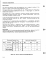
1
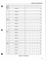
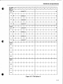
STD 7000
7704
BYTE-WIDE
Memory Card
USER'S MANUAL
o
o
NOTICE
The information in this document is provided for reference only. Pro-Log does not assume any liability arising
out of the application or use of the information or products described herein.
This document may contain or reference information and products protected by copyrights or patents and
does not convey any license under the patent rights of Pro-Log, nor the rights of others.
Printed in U.S.A. Copyright© 1981 by Pro-Log Corporation, Monterey, CA93940. All rights reserved. However,
any part of this document may be reproduced with Pro-Log Corporation cited as the source.
0
STD 7000
7704
BYTE-WIDE
Memory Card
USER'S MANUAL
()
..
.,
1/82
FOREWARD
This manual explains how to use Pro-Log's 7704 Byte-Wide Memory Card It is structured to reflect the answers
to basic questions that you, the user, might ask yourself about the 7704. We welcome your suggestions on how
we can improve our instructions.
o
The 7704 is part of pro-Log's Series 7000 STD BUS hardware. Our products are modular, and they are
designed and built with second-sourced parts that are industry standards. They provide the industrial
manager with the means of utilizing his own people to control the design, production, and maintenance of the
company's proucts that use STD BUS hardware.
Pro-Log supports its products with thorough and complete documentation. Also, to provide maximum
assistance to the user, we teach courses on how to design with, and to use, microprocessors and the STD BUS
products.
You may find the following Pro-Log documents useful in your work: Microprocessor User's Guide and the
Series 7000 STO BUS Technical Manual. If you would li.ke a copy of these documents, please submit your
request on your company letterhead.
()
o
ii
Contents
Page
•
Foreword -------------------------------~------------------
ii
Figures ---------------------------------------------------
v
Section 1 - Purpose and Main Features ---------------------
1-1
Section 2 - Installation and Specifications ---------------
2-1
Installation ---------------------------------------------Wire Jumpers ---------------------------------------------Memory Decoder -------------------------------------------Memory Type ----------------------------------------------Unused Sockets -------------------------------------------Memex ----------------------------------------------------Segment Select -------------------------------------------Specifications --------------------------------------------
2-1
2-3
2-4
2-22
2-25
2-25
2-26
2-26
Section 3 - Operation and Programming --------------------Introduction ---------------------------------------------Memex
3-1
3-1
3-1
Memex Example --------------------------------------------Memex Control Software Introduction ----------------------Memex Control Software Example One------------------------Memex Control Software Example Two -----------------------Memex Control Software Example Three ---------------------Memex Control Software Example Four ----------------------Memex Interrupt Control Software -------------------------Segment Select -------------------------------------------Segment Select Control Software ---------------------------
3-1
3-4
3-4
3-6
3-7
3-8
3-10
3-13
3-16
Section 4 - Operating Software ----------------------------
4-1
Section 5 - Maintenance ----------------------------------Reference Drawings ---------------------------------------Return for Repair Procedures -----------------------------Limited Warranty ------------------------------------------
5-1
5-1
5-4
5-4
iii
Figures
Figure
1-1
1-2
2-1
2-2
2-3
2-4
2-5
2-6
2-7
2-8
2-9
2-10
2-11
2-12
2-13
2-14
2-15
2-16
2-17
2-18
2-19
2-20
2-21
2-22
2-23
2-24
2-25
2-26
2-27
2-28
2-29
2-30
2-31
iv
o
Page
7704 Byte Wide Memory Card
Block Diagram of 7704 Byte Wide Memory Card -----7704 Installation -------------------------------Segment Select Interconnect ---------------------Part Numbers for 7704 Option Jumpers ------------Physical Location of Features -------------------7704 Memory Decoder Option ----------------------7704 Option 0 -----------------------------------7704 Option I -----------------------------------7704 Option 2 -----------------------------------7704 Option 3 -----------------------------------7704 Option 4 -----------------------------------7704 Option 5 -----------------------------------7704 Option 6a ----------------------------------7704 Option 7 -----------------------------------7704 Option 8 -----------------------------------7704 Option 9 -----------------------------------7704 Option 10 ----------------------------------7704 Option 11 ----------------------------------7704 Option 12 ----------------------------------7704 Option 13 ----------------------------------7704 Option 6b ----------------------------------7704 Option 15 ----------------------------------Socket Configurations ---------------------------Memory Components -------------------------------Electrical and Environmental Specifications -----Electrical Characteristics ----------------------Interface Specifications ------------------------Edge Connector Pin List -------------------------7704, Timing for Write --------------------------7704, Timing for Read ---------------------------7704, Memex Timing ------------------------------7704, Segments Timing ----------------------------
1-1
1-2
2-1
2-2
2-3
2-4
2-5
2-6
2-7
2-8
2-9
2-10
2-11
2-12
2-13
2-14
2-15
2-16
2-17
2-18
2-19
2-20
2-21
2-23
2-24
2-26
2-27
2-27
2-27
2-28
2-29
2-29
2-30
()
()
0
Figures (continued)
2-32
7704, Segments MEMRQ ----------------------------2-33
7704, RD* or WR* Timing -------------------------3-1
7704 Memex Example ------------------------------3-2
7704 Memex Example ------------------------------3-3
7704 Memex Software Example One -----------------3-4
7704 Memex Software Example Two -----------------3-5
7704 Memex Software Example Three ---------------3-6
7704 Running Example Three ----------------------3-7
7704 Memex Software Example Four ----------------3-8
7704 Running Example Four -----------------------Memex, Interrupt Software, Primary Memory -------3-9
7704, Memex, Interrupt Software Expanded Memory -3-10
7704 Memex, Interrupt Software Flow Chart -------3-11
3-12
7704 Segment Select Example One -----------------3-13
7704 Segment Select Example Two -----------------3-14
7704 Segment Control Software -------------------5-1
Schematic, 7704 ---------------.-----------------5-2
Assembly, 7704 -----------------------------------
2-30
2-31
3-2
3-3
3-5
3-6
3-7
3-8
3-9
3-9
3-11
3-11
3-12
3-14
3-15
3-16
5-2
5-3
•
v
_lIIiiiIMiliiDiUilililMJ.iiA. .""'MfuQJiJ'"WGiMWiD,AiM'OOdWbUJiUi&&IiiI.... it,hl#,;
MMf4ii14!iji\lF/i4Y ..~
o
o
o
vi
SECTION 1
Purpose and Main Features
e
()
•
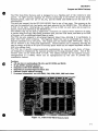
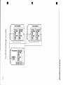
The 7704 Byte-Wide Memory card is designed to be a flexible part of the memory in your
system. Its eight sockets, designed for devices conforming to the tTEDEC 28 pin dual inline
standard pinout, allow the use of 2K, 4K, and 8K ROMs and RAMS all of one size or in
combinations.
The card can respond the the STD BUS MEMEX line in one of two ways. The memory on the
card can be separated into two banks, each bank selected by the MEMEX line. This allows up
to 64K on one card. Alternately, two cards, with up to 64K on each card, can be used in a
system, each card selected by the MEMEX line.
The MEMEX line can be used to implement a maximum of memory with a minimum of cards.
A system using Pro-Log's 7804 Z80A processor card, and two 7704 cards, can have up to 124K
of memory with no additional signal lines or cards.
The 7704 can also respond to an external Segment Select line, allowing it to participate in
large scale bank select schemes. The Segment Select line can be controlled by a memory
segment controller or by I/O ports. One output port can control eight 7704 cards. Also, it
can be tailored to fit small scale applications. Unused sockets can be disabled, allowing the
card to occupy as little as 2K bytes of memory space which can be mapped anywhere within a
64K byte address field.
The 7704 has 12 specific jumper-selectable combinations for memory parts. Some of these
are designed to complement the memory provided on Pro-Log processor cards. Any of the
memory parts can be either ROM or RAM. The address decoder for the specific memory
configurations is a PROM, which can be reprogrammed by the user to provide any
combination desired.
Features
* All one size or combinations 2K, 4K, and 8K ROMs and RAMs
* 28 pin JEDEC standard sockets
* Responds to STD BUS MEMEX line
* Responds to external Segment Select line
* Onboard fiexible address decoding
* Processor independent -use with 8085, Z80, 6800, 6809, 8088 and others
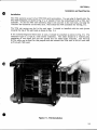
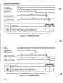
Figure 1-1. 7704 BYTE-WIDE Memory Card
1-1
Ptrpose and Main Feattres
()
MEMORY BANK
DATA
BUS
BUFFER
MEMEX~~--------~~-----------------i
CHIP
SELECT
DECODER
ADDRESS
BUS
BUFFERS
MEMRQ'~~_---I
CONTROL
BUS
BUFFER
AND
RD'--I------!READ/WRITE
LOGIC
WR'-I~_---I
o
L-------------------------------------------------------------~----------------------------r_-S~~L~~~T
7704
'ACTIVE LOW LEVEL LOGIC
SHADING INDICATES SOCKETS
Figure 1-2. Block Diagram of 7704 BYTE-WIDE Memory Card
u
1-2
SECTION 2
Installation and Specification
I)
Installation
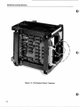
The 7704 operates as part of an STD BUS card rack system. You can plug it directly into the
STD BUS backplane, as shown in Fig. 2-1, or extend it from the motherboard with a 7901 card
extender. To use the 7901 card extender, plug it into any slot in the card rack, and plug the
7704 into the connector on the 7901 card. This makes the 7704 accessible for testing, etc.
The 7704 can occupy any slot in the card cage. It should be installed with the card ejector
towards the top of the card rack as shown in Fig. 2-l.
If the external Segment Select line is used, it should be attached as shown in Fig. 2-2. The
connector type is a 2-pin 0.1 inch center connector. The cable should be a twisted pair,
consisting of one signal line and one ground line for added noise immunity. The Pro-Log
RC704 cable can be used for this purpose and can connect the 7704 card to an I/O card such
as Pro-Log's 7605 card.
()
•
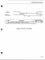
Figure 2-1. 7704 Installation
2-1
Installation and Specification
o
o
Figure 2-2. 7704 Segment Select Connector
o
2-2
Installation and Specification
o
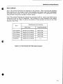
WIRE JUMPERS
Some 7704 optional functions are selected by wire jumpers. When removing and replacing
these jumpers, cut the jumper in half, then desolder and remove each half individually.
Remaining solder should be removed, and new jumpers installed in the appropriate places.
This procedure will prevent damage to circuit traces.
Most 7704 optional functions are selected by permanent 0.025 in. squa.re posts which can be
connected by slip on, slip off connectors. Part numbers for these connectors and headers
are listed in Fig. 2-3. Figure 2-4 shows the location of these jumpers and some of the other
features of the 7704.
Manufacturer Part Number
Part
Elco Corp.
Berg Electronics
2 Pin Header
00
02 32 00 852
6561.1-102
4 Pin Header
00 8261 04 32 00 852
65611-104
6 Pin Header
00 8261 06 32 00 852
65611-106
8 Pin Header
00 8261 08 32 00 852
65611-108
Connector
00 8261 02 42 00 870
~261
-
()
Figure 2-3. Part Numbers for 7704 Option Jumpers
•
2-3
Installation and Specification
o
W8
WU
~) OOlo-QD-o
lo o-olC>-Q!]-o
I.
Rl
0
0
0
0
W.g :
01
0
C2
P.::c2O~.,g",74L.,g",U:..D..245~~"
csfOl
lQQ]
[QJ
,
'0
0
I_ 0
.2
0
0
0
[8]
C3
C6 0
20
,
US
74LS244
0
0
0
0
0
0 0 ,:
R=/14
[QJ,
w
0
0
0
0
0
0
0
0
0
0
0
0
0
0
0
0
0
0
00 0
~
~gl
Wl0:lt
01
0
0
00
0
0
C13
,.
o
0
0
0
0
0
0
0
0
0
0
0
0
0
o
0
0
0
0
o
0
0
o
0
o
0
o
0
:It
>5
IIEII 2
0
W12
...--.. rl FI
m c.~
55
\.Qi!J
W1
W2
[I
ro
"
'c-cr--.::r-cr--o-tr-u-tT~'o
C12~
0
0
0
0
o
"
t)
0
0
o
2
o
0
0
"
o
0
0
0
0
0
0
0
0
0
0
0
•
0
0
•
0
"
0
•
M
I
o-[!![]-o
o
0
0
o
0
o
0
W
o-[!!D-o
0
0
0
o
0
~
0
o
0
0
0
IIEII 6
o
CI6
o
15
0
(OJ
0
28
0
0
0
<)
1
0
0
~
0
0
0
C 14
f3]
0
0
"
CIS
0
o
IIEII 5
0
o
0
21
M
0
o
o-{]jD-o
0
0
000000
,
0
101
0
0
15
0
15
0
0
II Ell 4
0
IIEII 3
,
o
o
a'll
0
0
0
~
0
o
0
,
[QQl
0
•
'If 16
C4
v
21
~
~II
0
IIEII 1
"R5l
C10lQj,
'0
IQI
W
16
00
1001
0
llEll 0
c9fOl
~
W3[1
F.a
I
~
[0
00
o
o
w
0
0
0
0
o
o
0
0
0
0
o
0
0
o
0
0
0
o
0
o
0
0
0
o
0
0
11
21
o
IIEII 7
,.
,
0
0
0
o
0
0
o-L1@J-o
o
0
o
0
0
0
0
0
o
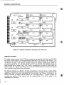
Figure 2-4. Physical Locations of Features on the 7704 Card
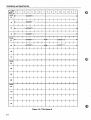
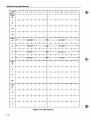
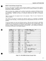
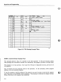
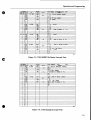
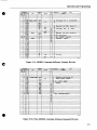
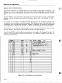
MEMORY DECODER
The eight memory sockets of the 7704 can accept any comhiantion of 2K, 4K, and 8K ROMs
and RAMs which conform to the specifications described in the Memory Type section. The
combination of memory sizes and the address range each socket occupies are controlled by
the Memory Decoder. The Memory Decoder contains 12 optional combinations, which are
selected by jumper W4 1-2, 3-4, and jumpers W5, 1-2, 3-4, and 5-6. The physical locations of
these jumpers can be found in Fig. 2-4. The 12 combinations and how to select them are
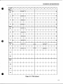
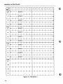
shown in Fig. 2-5. Figures 2-6 through 2-21 are 64K memory maps which show the address
field occupied by each socket for each option.
The Memory Decoder is a PROM. If other combinations of memory types or other address
mapping is required, the PROM can be programmed with your own option. Two sections of the
PROM have been left blank specifically for this purpose. The options contained in the
Memory Decoder as shipped should suffice for most applicaitons. If other options are
required, the writing of the program and the programming of the PROM would be the
responsibili ty of the user.
2-4
0
•
e
MEMORY
PARTS
BY SIZE
JUMPERS
OPTION
(X = JUMPER INSTALLED)
I
W5
W4
5-6
3-4
1-2
1-2
X
X
X
X
1
-
X
X
2
X
-
I-J:j
3
-
~.
4
3-4
TOTAL
MEMORY
ADDRESS
RANGE
o
MEMORY PER SOCKET
COMMENTS
0
1
2
3
4
5
6
7
8000-DFFF
4
4
4
4
2
2
2
2
Standard as shipped from Pro-Log (4K, 2K mixed).
40K
0000-9FFF
8
8
8
8
2
2
2
2
8K, 2K mixed.
0
48K
OOOO-BFFF
8
8
8
8
4
4
4
4
8K, 2K mixed.
0
0
64K
OOOO-FFFF
8
8
8
8
8
8
8
8
A118K.
0
0
8
16K
4000-7FFF
2
2
2
2
2
2
2
2
All 2K.
-
0
8
0
32K
8000-FFFF
4
4
4
4
4
4
4
4
AII4K.
-
X'
4
0
0
32K
8000-FFFF
8
8
8
8
-
-
-
-
This option and option 6b go together. The MEMEX line is tied
to decoder PROM input A8, so a low MEMEX state will select 6a,
and a high will select 6b.
-
X
-
-
-
-
-
-
-
-
-
-
-
Not programmed. Intentionally left blank for customer's own
configu ration.
X
X
-
-
0
4
4
24K
0000-5FFF
4
4
4
4
2
2
2
2
4K, 2K mixed; alternate standard.
-
X
X
-
-
0
1
7
18K
3800-7FFF
2
2
2
2
2
2
2
4
Use with 7804's standard configuration: three 4K ROM and one
2K RAM. Total memory on both cards is 32K. If all 4Ks are
ROM and all 2Ks are RAM, you have 16K ROM and 16K RAM.
10
X
-
X
-
-
0
5
3
26K
1000-1 FFF
2800-7FFF
4
2
2
2
4
4
4
4
Use with 7880 which has 4K ROM and 2K RAM. Option does not
have consecutive addresses. Total memory for both cards is
32K. If all 4Ks are ROM and all 2Ks are RAM, you have 24K ROM
and 8K RAM.
11
-
-
X
-
-
0
8
0
32K
0000-7FFF
4
4
4
4
4
4
4
4
All 4Ks. Like option 5 except occupies addresses 0000-7FFF.
12
X
X
-
-
-
0
0
8
16K
0000-3FFF
2
2
2
2
2
2
2
2
All 2Ks. Like option 4 except occupies addresses 0000-3FFF.
13
-
X
-
-
X"
0
8
0
32K
7FFF-00OO
4
4
4
4
4
4
4
4
Test option for Pro-Log use only.
X
-
-
-
X·*
4
0
a
32K
8000-FFFF
-
-
-
-
8
8
8
8
Dual bank for 2764s; to work with option 6a using MEMEX high
to select.
-
-
-
-
-
-
-
-
-
-
-
-
-
-
-
Not programmed. Intentionally left blank for customer's owm
configuration.
8K
4K
2K
-
0
4
4
24K
X
-
4
0
4
X
X
-
4
4
-
X
X
-
8
X
X
-
X
-
5
-
X
-
X
6a
X
-
-
7
-
-
~
8
X
i
9
As
Shipped
~
~
.J,
a:
(t)
:;
~
~
-
-
-
o
~
....
~
6b
15
Uses MEMEX with a low state at W4.
Uses MEMEX with a high state at W4.
-
-
-
I
,...
....
o
=
~
C'Il
1.............
~
~
I
c.n
,...
=
....
8
Installation and Specification
F
PAGE
OX
14------
SOCKET 0 - - - - - - - I f - - - - - - - - - - - - - - - - - + I
1X
14------ SOCKET 1
2X
14----------S0CKET2--------~------------------~
3X
~
1~--------SOCKET3--------r-------------------------.1
PAGE
4X
o
•
•
1~---------SOCKET4---------~~~14~~--------SOCKET5----------~~~1
5X
6X
7X
o
PAGE
ex
9X
AX
BX
PAGE
ex
OX
EX
FX
Figure 2-6. 7704 Option 0
2-6
o
Installation and Specification
e
MSO
~
PAGE
OX
0
I
2X
3X
I
I
4
I
I
I
I
~
5
I
6
I
al91AI BI Cl DIEI
7
I
I
I
I
I
I
I
I
I
I
I
I
I
I
I
I
I
I
I
I
I
I
I
I
I
I
I
I
I
I
I
I
I
I
I
I
I
I
I
I
I
I
I
I
I
I
I
I
I
I
I
I
I
I
I
I
I
I
I
I
I
I
I
I
I
I
I
I
I
I
I
I
I
I
I
I
I
I
I
I
I
I
J
I
I
I
I
I
I
I
I
I
I
I
1
J
t
I
I
I
I
I
J
J
4
I
I
I
I
I
I
I
I
I
I
I
I
I
I
I
I
SOCKET 2
I
I
..........
I
I
I
I
I
I
I
I
I
I
I
I
I
I
I
I
I
I
I
I
I
~
I
I
I
I
I
I
I
I
I
I
I
I
I
I
I
I
J
I
I
I
I
I
J
J
I
I
I
I
I
I
I
1
I
J
I
I
SOCKET 3
I
I
I
I
I
I
I
SOCKET 4
I
I
I
I
I
I
~
I
I
I
~
I
I
I
I
I
I
I
I
I
I
I
I
I
I
I
I
I
I
I
I
1
1
I
I
I
...
.
I
I
I
I
I
I
I
J
I
SOCKET 5
I
I
I
I
I
I
I
I
I
I
SOCKET 7
I
I
I
I
I
I
I
I
I
I
I
I
~
SOCKET 6
I
I
I
I
I
I
I
I
I
I
I
I
I
.....
.....
.
I
SOCKET 3
I
.....
.
I
I
I
.....
_JIOO.
I
I
F
_
SOCKET 2
I
9X
I
4
I
~
I
ax
I
SOCKET 1
I
I
PAGE
3
SOCKET 1
I
()
I
I
I
7X
I
I
I
6X
I
SOCKET 0
I
5X
2
SOCKET 0
4
PAGE
4X
I
•
I
I
1X
1
.....
.....
•
I
•
I
AX
I
I
I
I
I
I
I
I
I
I
I
I
I
I
I
I
I
I
I
I
I
I
I
I
I
I
I
I
I
I
I
I
I
I
ax
PAGE
I
I
I
I
I
I
I
I
I
ex
I
I
I
I
I
I
1
I
J
I
I
I
I
I
I
I
I
I
I
I
I
I
I
I
I
I
I
I
I
I
I
I
I
I
I
I
I
J
I
I
I
I
I
I
I
ox
I
I
I
I
I
I
I
I
I
I
I
I
EX
•
I
I
I
I
I
I
I
I
I
I
I
I
I
I
I •
I
I
I
I
I
I
I
I
I
I
I
I
I
I
I
I
I
I
I
I
I
I
I
I
I
FX
Figure 2-7. 7704 Option 1
2-7
---~~-~~---~----
...- ....---.~-----.---.~-. -.--".-~-.~.-- •.. --.---~..---.... -.- .... " ...........
.
Installation and Specification
MSO
I~
PAGE
ox
1X
2X
0
1 1
7X
I
I
I
I
I
I
I
I
I
I
I
T
ax
I
I
I
I
I
I
till
PAGE
I
I
I
I
I
I
I
I
I
I
I
I
I
I
I
I
I
I
I
I
I
I
I
I
I
I
I
I
I
I
I
I
I
I
I
I
,I
I
I
I
I
I
I
I
I
I
I
I
I
I
I
I
I
I
I
T
I
I
I
I
I
I
I
I
I
I
I
I
I
T
I
I
I
I
I
I
I
I
I
I
I
I
I
I
I
I
I
I
SOCKET 2
I
I
I
I
I
I
I
I
I
I
I
I
I
I
I
SOCKET 2
I
I
I
I
I
I
I
I
I
I
I
I
I
I
I
SOCKET 3
I
I
I
I
I
I
I
I
I
I
I
I
I
I
I
I
SOCKET 4
I
I
I
I
I
I
I
I
I
I
I
I
I
I
I
I
I
I
I
I
I
I
I
I
1
I
I
1
I
1
I
I
I
I
I
I
I
I
I
I
I
I
I
I
I
I
I
I
I
I
I
I
I
I
I
I
I
I
I
I
T
I
I
I
I
I
SOCKET 3
I
I
I
I
I
I
I
I
I
I
I
I
ax
I
I
I
I
till
...
I
I
I
I
I
AX
I
I
I
I
I
I
9X
I
I
I
r
SOCKET 1
I
.I
I
I
I
I
SOCKET 1
I
I
I
till
..
I
SOCKET 0
I
I
...
I
I
SOCKET 5
I
I
I
I
I
I
SOCKET 6
I
I
I
I
I
I
1
I
I
I
I
I
I
I
I
r
I
I
I
I
I
I
I
I
I
I
I
I
I
I
I
I
I
I
....
.....
.....
....
.....
.....
......
o
....
.....
...
......
SOCKET 7
I
I
o
F
.....
I
I
PAGE
IAI BI Cl OIEI
9
I
till
...
I
I
I
6X
8
I
~
...
7
I
I
5X
I5 I6 I
I
.....
PAGE
till
4X
1 4
SOCKET 0
III
I
3X
1 2 1 3
I
I
I
I
I
I
I
I
I
I
I
1
T
I
I
I
I
r
I
I
ex
ox
I
I
I
I
I
I
I
I
I
I
I
I
I
I
I
I
I
I
I
I
I
I
I
I
I
I
I
I
I
I
I
I
I
I
I
I
I
J
I
I
I
I
I
I
I
I
I
I
I
I
I
I
I
I
I
I
I
I
I
I
I
I
I
I
I
I
I
I
EX
I
I
I
I
I
I
I
I
I
I
I
I
I
I
I
I
I
I
I
I
I
I
I
I
I
I
I
I
I
I
FX
Figure 2-8. 7704 Option 2
2-8
o
Installation and Specification
o
~
0
MSD
PAGE
OX
1X
2X
1 1 1 2 13 1 4 15 16 1
...
...
...
PAGE
4X
I
I
I
I
I
I
I
I
AX
PAGE
ex
•
I
I
I
J
I
I
I
I
I
I
I
I
I
I
I
I
J
I
I
I
I
I
I
I
I
I
I
I
I
I
I
I
I
I
I
I
......
I
I
I
I
I
I
I
I
I
I
I
I
I
I
I
I
......
--...
...
I
I
I
I
I
I
I
I
I
I
I
I
I
I
I
I
I
I
I
I
I
I
I
I
I
I
I
I
I
....
SOCKET 2
I
I
I
I
I
I
I
I
I
I
I
I
I
I
I
I
I
I
...
I
I
I
I
I
SOCKET 2
I
I
I
I
I
I
SOCKET 3
I
I
I
I
I
I
SOCKET 3
I
I
I
I
I
I
I
I
I
I
1
I
I
I
I
I
1
I
I
J
I
I
I
I
I
I
I
I
J
I
I
I
I
I
I
I
I
I
I
I
I
I
I
I
I
I
I
I
I
I
I
I
I
I
I
I
I
I
I
I
I
I
I
I
I
I
I
I
I
J
I
I
I
I
SOCKET 4
I
I
I
I
I
I
SOCKET 5
I
I
I
I
I
I
SOCKET 6
I
I
I
I
I
I
I
I
I
I
I
I
I
I
I
I
I
I
I
I
I
I
I
I
I
I
I
I
I
I
I
I
I
I
I
I
I
I
I
I
I
I
I
I
I
J
I
I
I
I
I
I
I
I
I
J
I
I
I
I
I
I
I
I
I
I
I
I
I
I
I
I
I
I
I
I
I
I
I
I
I
1
I
I
I
I
I
I
SOCKET 6
I
I
I
I
I
I
I
I
SOCKET 7
I
I
I
I
I
I
1
I
I
I
I
I
I
I
I
I
I
I
I
I
......
.
.....
.....
--...
...
..
...
I
I
I
I
I
I
I
I
I
I
I
I
I
I
I
I
I
I
SOCKET 7
I
.
...
I
I
I
....
...
I
I
I
......
I
I
I
I
....
I
I
I
I
SOCKET 4
I
I
I
-
I
I
I
I
I
I
SOCKET 5
I
1
I
I
I
I
I
I
I
I
I
I
~
I
~
...
I
I
I
I
FX
I
I
I
...
...
I
I
I
EX
I
I
...
....
I
I
I
I
ox
I
II1II
...
I
I
I
I
ex
1
1l1li
...
I
I
I
I
9X
I
I
I
I
ax
I
I
I
I
PAGE
I
I
...
SOCKET 1
I
7X
.
SOCKET 1
I
6X
I
I
...
...
F
SOCKET 0
I
5X
Sl91AI al Cl DIE 1
SOCKET 0
I
I
3X
7
.
_
...
1
I
I
I
I
I
I
I
I
I
Figure 2-9. 7704 Option 3
2-9
Installation and Specification
o
F
PAGE
ox
1X
2X
3X
PAGE
4X
...
5X
~
6X
...
7X
~
SOCKET 0
SOCKET 1
•
•
•
•
PAGE
0
ax
9X
AX
BX
PAGE
ex
ox
EX
FX
o
Figure 2-10. 7704 Option 4
2-10
Installation and Specification
•
MSO
~
o
1
1
I
2
1
3
I
4
I
5
1
6
I
7
al91AI
al Cl OIEI
F
PAGE
OX
I
I
I
I
I
I
I
I
I
I
I
I
I
I
I
I
I
I
I
I
I
I
1
1
I
1
I
I
I
I
I
I
I
I
1
~
J
I
I
I
I
1
I
I
I
I
I
I
I
I
I
I
I
I
1
I
1
I
I
I
I
I
I
I
I
I
I
I
I
I
I
I
I
I
I
I
I
I
J
I
I
I
I
I
I
I
I
I
l
I
I
I
I
I
I
I
I
I
I
I
J
I
I
I
I
I
I
I
1
I
I
I
I
I
I
I
I
I
I
I
I
I
I
I
I
I
I
I
I
I
I
I
I
I
I
I
1X
J
I
I
2X
I
I
3X
PAGE
4X
I
I
I
I
I
I
I
I
I
I
I
I
I
I
I
f
I
I
I
I
I
I
1
J
I
I
I
I
I
I
I
I
5X
I
I
I
I
I
I
I
I
I
I
I
I
I
I
I
1
1
1
1
f
I
I
1
I
I
I
I
I
I
I
6X
I
I
I
I
7X
PAGE
ax
I
•
I
I
9X
•
I
I
AX
•
ox
I
•
I
I
I
I
I
....
I
I
I
I
....
•
•
I
I
I
I
I
I
I
I
I
I
I
I
I
I
I
I
I
SOCKET 3
I
I
I
I
I
I
I
I
I
I
I
I
I
I
I
I
I
I
I
J
I
I
I
I
I
I
I
I
I
I
I
I
I
I
I
I
I
I
I
I
I
I
I
I
I
I
I
I
I
I
I
I
I
I
I
I
I
I
I
I
I
I
I
I
I
I
I
I
I
I
I
I
I
I
I
I
I
I
I
I
I
I
I
I
I
I
I
I
I
I
I
I
I
I
I
I
I
I
I
I
I
I
I
I
I
I
I
I
I
I
I
I
I
I
I
I
I
I
I
I
I
I
I
I
SOCKET 6
I
I
I
I
I
I
I
I
I
I
I
......
I
...
~
I
I
I
I
I
I
I
I
I
I
I
I
I
I
I
I
I
I
I
I
I
I
I
SOCKET 7
I
...
......
I
I
......
I
I
I
I
I
...
~
SOCKET 5
I
......
I
SOCKET 4
I
FX
I
I
SOCKET 1
I
I
I
I
I
I
J
I
EX
I
I
SOCKET 0
I
I
I
I
I
I
....
PAGE
ex
i
SOCKET 2
I
ex
I
1
1
Figure 2-11. Option 5
I
I
......
2-11
22&CUSQ£&d-
_=_"",,""#1\=="1,"="',£_,==;1 '.tiW;'; ;,;;';:,4."
4;41&
;,14.41'
4#¥#fP&
Installation and Specification
MSO
~
PAGE
OX
0
I
2X
I
I I
4
5
6
I
7
a
I 91AI
81 Cl OIEI
I
I
I
I
I
I
I
I
I
I
I
I
I
I
I
I
I
I
I
I
I
I
I
I
I
I
I
I
I
I
I
I
I
I
I
I
I
I
I
I
I
I
I
1
1
I
1
I
I
I
I
I
I
I
,I
I
I
I
I
I
I
I
I
I
I
I
I
1
I
I
I
I
I
I
I
I
I
I
SOCKET 1
I
I
,
I
I
I
I
I
I
~
I
I
T
I
I
I
SOCKET 2
1
I
ill
I
I
I
I
1
I
I
I
I
I
I
SOCKET 2
J
I
I
I
....
....
.....
.
~
I
I
I
I
SOCKET 3
I
I
I
I
I
I
I
I
I
I
I
I
I
I
I
I
I
I
I
--.
p
I
I
I
I
I
I
I
I
I
I
I
I
I
I
1
I
I
I
I
I
I
I
I
I
I
I
I
I
I
I
1
1
I
I
I
I
I
I
I
I
I
I
I
I
I
T
I
T
I
I
I
I
I
1
1
I
I
I
I
I
I
I
I
I
I
1
1
I
SOCKET 3
I
I
I
I
I
I
ill
I
I
o
F
~
I
I
I
PAGE
3
I
I
I
SOCKET 1
1
I
7X
I
1
I
I
•
J
J
I
I
6X
J
SOCKET 0
~
PAGE
ill
4X
5X
1
I
~
•
2
SOCKET 0
I
3X
1
•
I
I
1X
1
I
I
I
I
I
I
I
.....
-...
o
ax
I
I
I
I
I
I
I
I
I
I
I
I
I
I
I
I
I
I
I
I
I
I
I
I
I
I
I
I
I
I
I
I
I
I
I
I
I
I
I
I
I
I
I
I
I
I
I
I
I
I
I
I
I
I
I
I
I
I
I
I
I
I
I
I
I
I
I
I
I
I
I
I
I
I
I
I
I
I
I
I
I
I
I
I
I
I
I
I
I
I
I
I
I
I
I
1
I
J
I
I
I
I
1
I
I
I
I
I
I
I
I
I
I
I
I
I
I
J
J
I
I
I
I
I
J
I
I
I
I
I
I
I
I
I
9X
I
AX
I
I
BX
PAGE
I
I
ex
I
I
I
ox
I
I
I
I
I
I
I
I
I
I
I
I
EX
I
I
I
I
I
I
I
I
I
I
I
I
I
I
I
I
1
I
I
I
I
I
I
I
I
I
I
I
I
I
I
I
J
J
I
I
I
I
I
I
I
FX
Figure 2-12. 7704 Option 6a
2-12
o
Installation and Specification
F
PAGE
OX
1X
2X
3X
PAGE
4X
5X
6X
7X
PAGE
ax
9X
AX
BX
PAGE
ex
OX
EX
•
FX
Figure 2-13. 7704 Option 7
2-13
Installation and Specification
MSO
~
o
I
1
12 I
3
I
I
4
5
I
6
I
a
7
I
9
IAI BI Cl OIEI
o
f
PAGE
OX
I
I
I
I
I
I
I
I
I
I
I
I
I
I
T
T
r
I
I
I
I
I
I
I
I
I
I
I
1X
I
I
I
I
I
I
I
I
I
T
I
I
I
I
I
I
I
I
I
I
I
I
I
I
I
I
I
I
I
I
I
I
I
I
,
,I
,I
I
I
I
I
I
I
I
I
I
I
I
I
I
I
I
I
I
I
I
I
I
I
I
I
2X
I
3X
PAc:;E
4X
I
I
I
I
I
I
I
I
I
I
I
I
I
I
I
I
I
I
I
I
I
I
I
I
I
I
I
I
I
I
I
I
l
I
I
I
I
I
I
I
I
I
I
I
I
I
I
T
I
I
I
I
I
I
I
I
I
I
I
I
I
I
I
SOCKET 0
I
I
I
I
I
I
I
I
I
I
I
I
I
I
I
I
I
I
I
I
I
I
I
I
I
I
I
I
I
I
I
I
I
I
I
I
I
I
I
I
I
I
I
I
I
I
I
I
I
I
I
I
I
I
I
I
I
I
5X
I
I
I
I
I
I
I
I
I
I
I
I
I
I
I
I
I
6X
I
I
I
I
7X
PAGE
ax
I
I
I
I
~
I
9X
I
AX
ax
PAGE
ex
ox
I
I
I
I
I
I
SOCKET 1
I
I
I
~
I
I
I
~
I
I
I
I
I
I
I
I
I
I
I
I
T
T
T
J
I
I
I
I
I
I
I
I
I
I
I
I
I
I
I
I
I
I
I
I
I
I
I
I
I
I
I
I
I
I
I
I
I
I
I
SOCKET 5
I
I
I
I
I
I
I
SOCKET 2
I
I
I
I
I
I
~
I
I
I
I
I
I
I
I
I
I
I
I
I
I
I
SOCKET 4
I
I
I
I
....
I
I
I
I
I
I
III
I
I
I
I
I
I
I
I
I
I
I
I
I
-.....
~
I
I
I
J
I
I
~ ~
SOCKET 6
I
I
......
..
.
~
SOCKET 3
I
()
I
I
I
I
I
I
~
I
I
I
I
I
I
I
I
I
I
I
I
SOCKET 7
I
I
I
I
I
I
I
I
I
I
I
I
I
I
I
I
I
I
I
I
I
I
I
I
.....
I
•
I
EX
I
I
I
I
I
I
I
I
I
I
I
I
I
I
I
I
I
I
I
I
I
FX
2-14
I
I
I
I
I
Figure 2-1.4. 7704 Option 8
I
o
Installation and Specification
•
F
PAGE
OX
1X
2X
3X
PAGE
~
SOCKET 1
5X
~
SOCKET 3
6X
~
SOCKET 5
7X
~
4X
•
~
SOCKET 0
~
SOCKET 2
•
• ...
~
•
•
•
•
SOCKET 4
SOCKET 6
PAGE
ax
9X
AX
ex
PAGE
ex
OX
EX
•
FX
Figure 2-15. 7704 Option 9
2-15
'W_--:a:wwaaaWMliWilWWi&GiMMLIA&akM.m===IM&MlQI&AilQ&i'MAWiAlauumii3liiWalNi;U;UN.' •••"ULR4S:,J
"u.
PI ,%
,,4 h'
"
;;
II,M'» 4,
Installation and Specification
MSO
~
o
1
1
121314151617
8
1
9
1 Al
B
1 cJ
DIE 1
o
F
PAGE
OX
1X
I
I
I
I
I
I
I
I
I
I
I
I
I
I
~
I
I
I
I
I
I
I
I
I
I
I
I
I
I
I
I
I
I
I
I
I
I
I
I
I
I
I
I
I
I
I
I
T
I
I
I
I
I
SOCKET 2
SOCKET 4
I
I
I
I
I
I
I
I
SOCKET 5
I
I
I
I
I
I
I
~
I
PAGE
I
I
I
7X
I
~
PAGE
"III
4X
6X
I
I
I
I
I
I
I
I
I
I
I
I
I
I
I
I
SOCKET 1
I
I
I
I
I
I
I
I
I
I
I
I
1
T
I
1
I
I
I
1
I
I
I
1
I
I
I
~
I
5X
I
I
I
SOCKET 0
2X
3X
I
I
I
I
~
I
I
I
•
~
1
I
1
I
SOCKET 3
I
r
•
I
,I
I
I
I
I
I
I
I
I
I
I
I
I
I
I
I
I
I
I
I
I
I
I
I
I
~
I
I
I
I
I
I
I
I
I
......
I
I
I
I
I
I
I
I
I
I
I
I
SOCKET 7
I
I
I
I
I
I
I
I
I
I
I
I
I
I
I
I
I
I
I
I
I
I
I
~
I
•
......
SOCKET 6
I
....
I
I
I
I
I
I
I
I
I
I
I
I
I
1
I
I
1
I
I
I
I
I
I
I
I
I
I
I
I
I
I
I
I
I
I
I
I
I
T
I
I
I
I
I
I
I
I
I
I
1
I
1
I
.......
o
ax
I
I
I
I
I
I
I
I
I
I
I
I
I
I
I
I
I
I
I
I
I
I
I
I
I
I
I
I
I
I
I
I
I
I
I
I
I
9X
I
I
AX
I
I
I
-r
I
I
I
I
I
I
I
I
I
I
I
I
I
I
I
I
I
1
I
I
I
I
I
I
I
I
I
I
I
I
I
I
I
I
BX
PAGE
I
ex
I
I
I
I
I
I
I
I
I
I
I
I
I
I
I
I
I
I
I
I
I
I
I
I
I
I
I
I
T
I
I
T
I
I
I
I
I
I
I
I
I
I
I
I
I
I
I
I
I
I
I
I
ox
I
I
I
I
I
I
EX
I
I
I
I
I
I
I
I
I
I
I
I
I
I
I
I
I
I
I
I
I
I
I
I
I
I
I
I
I
I
I
I
I
I
I
I
I
I
I
I
FX
Figure 2-16. 7704 Option 10
2-16
o
Installation and Specification
o
MSO
I~
PAGE
ox
1X
0
I
I
I
I
I
....
I
7
a
I
9
IAI BI Cl DIEI
I
I
I
I
I
I
SOCKET 1
I
I
I
I
I
I
SOCKET 2
I
I
I
I
I
I
I
I
1
I
I
I
I
I
I
I
I
I
I
I
I
I
I
I
.....
I
I
I
I
I
I
I
I
I
I
I
I
I
I
I
I
I
I
--......
I
I
I
I
I
I
I
I
I
I
I
I
I
I
I
I
I
I
I
I
I
I
I
I
I
I
I
I
I
I
I
I
I
I
I
I
I
I
I
I
I
I
r
I
I
,
I
I
I
I
I
I
I
I
1
I
I
1
SOCKET 4
I
I
....
I
I .
I
I
I
I
I
I
I
I
I
I
SOCKET 5
I
I
I
I
I
SOCKET 6
I
I
I
~
I
I
I
I
I
I
I
I
I
I
I
I
I
I
I
I
I
I
I
I
I
I
I
I
SOCKET 7
I
I
I
I
I
I
I
I
I
I
I
J
1
I
I
I
I
I
I
I
I
I
1
1
I
I
I
I
I
I
I
I
1
I
I
I
I
L
I
,
I
I
I
I
F
.....
I
I
PAGE
6
I
~
•
I5 I
4
~
I
7X
I3 I
SOCKET 3
I
6X
I
I
....
I
5X
1
I
....
I
PAGE
4X
2
SOCKET 0
L
3X
I
•
I
I
2X
1
I
I
I
I
I
I
I
I
I
I
I
I
I
I
I
I
I
I
I
I
......
......
I
I
I
.....
....
I
...
--""
I
I
I
I
I
I
I
I
I
I
I
I
I
1
1
I
I
I
1
ax
I
I
I
I
I
I
I
I
I
I
I
I
I
,
I
I
I
I
I
I
I
I
I
I
I
9X
I
AX
I
I
I
I
I
I
,
I
I
I
I
I
I
I
I
I
I
I
I
I
I
I
I
I
I
I
I
I
I
I
I
I
I
I
I
I
I
I
I
I
I
I
I
I
I
I
I
I
I
I
I
I
I
-I
I
I
I
I
I
I
I
I
ex
PAGE
I
ex
ox
I
I
I
I
I
I
I
I
I
I
I
I
I
I
I
1
1
I
I
I
I
I
I
1
I
I
I
I
I
I
I
I
I
I
I
I
I
I
I
I
I
EX
•
I
I
I
I
I
I
I
I
I
I
I
I
I
I
I
L
I
I
I
I
I
I
I
I
I
I
I
I
I
I
I
I
I
I
I
I
I
I
I
1
FX
Figure 2-17. 7704 Option 11
2-17
Installation and Specification
PAGE
OX
~
SOCKET 0
1X
~
SOCKET 2
2X
...
SOCKET 4
3X
...
SOCKET 6
.
...
• ...
• ...
•
~
0
F
SOCKET 1
•
SOCKET 3
•
SOCKET 5
•
SOCKET 7
•
PAGE
4X
5X
6X
7X
o
PAGE
8X
9X
AX
BX
PAGE
ex
OX
EX
FX
Figure 2-18. 7704 Option 12
2-18
o
Installation and Specification
e
MSD
~
PAGE
OX
1X
0
I
I
I
I
I
I
I
I
•
I
I
a191AI BI Cl OIEI
I
1
I
I
I
I
I
I
I
I
I
I
r
T
T
T
I
I
I
I
I
I
I
I
I
I
\
\
I
I
I
I
I
T
T
1
I
I
I
I
I
I
I
I
I .
I
I
I
. I
\
\
\
\
I
I
1
I
I
I
I
I
I
I
I
I
I
I
I
I
I
r
I
I
.......
I
I
I
I
I
I
I
I
I
I
I
\
I
I
I
I
r
I
I
I
SOCKET 2
I
I
I
I
I
1
I
I
I
I
I
I
I
I
•
I
I
I
I
I
I
I
I
.......
I
I
I
I
I
I
r
r
I
I
I
I
I
·SOCKET 0
I
I
I
I
I
I
I
r
I
I
I
I
I
I
I
1
I
I
I
I
I
I
I
I
I
I
I
I
I
I
I·
I
4
I
I
I
\
I
.I
I
I
I
I
I
I
I .
I
I
I
I
I
I
I
I
I
I
I
I
I
I
I
I
I
I
I
I
I
I
I
I
I
\
I
I
I
I
I
I
I
I
I
I
I
.......
I
SOCKET 1
I.
......
....
...
I
I
F
..
SOCKET 3
I
I
PAGE
7
SOCKET 4
\
7X
I5 I6 I
SOCKET 5
I
6X
I
I
4
•
4
SOCKET 6
I
I
5X
I3 I
I
•
PAGE
4
4X
2
SOCKET 7
\
3X
I
•
\
2X
1
....
....
....
ax
I
I
I
I
I
\
I
I
I
I
I
I
I
I
I
1
\
1
I
\
I
I
I
I
I
I
I
I
I
I
\
.\
\
I
I
I
J
I
I
I
I
9X
I
I
I
T
T
I
I
I
AX
I
I
I
I
I
I
I
I
I
I
I
I
1
I
I
I
I
I
I
I
I
I
I
I
I
I
I
J
I
1
I
I
1
J
I
I
I
I
I
I
I
I
I
I
I
I
1
1
I
I
I
I
I·
I
I
I
I
I
T
I
I
I
I
I
J
I
I
1
I
1
I
BX
PAGE
ex
I
I
I
I
I
I
I
I
I
I
T
1
I
I
I
1
I
I
I
I
I
I
I
1
r
I
T
r
1
ox
1
I
I
1
J
I
I
I
I
I
EX
I
•
I
I
I
1
I
I
I
I
I
I
I
I
I
I
I
1
I
I
I
I
I
I
1
I
I
I
I
I
I
I
I
I
I
I
I
I
I
I
I
FX
I
Figure 2-19. 7704 Option 13
2-19
_ _.......'dlliWMWIU4i&Q&iIlWNiil&iiiPMWi4iitM&iJMbltt-=======aiiQ.: "". Mr:4#,4mkC; i
,4i %$
;
#T4#M¥A £¥¥ll4 HUhh 14M,
, #4, A
$ i
Installation and Specification
MSO
~
oI
1
121314151617
al91AI al Cl OIEI
o
F
PAGE
OX
I
I
I
I
I
I
I
I
I
I
I
I
I
I
I
I
I
I
I
I
I
I
I
I
I
I
I
I
I
I
J
I
I
I
I
I
I
I
I
I
1
I
I
I
I
I
I
I
I
I
I
L
I
I
I
I
I
I
I
I
I
,
I
I
I
I
I
I
I
I
I
I
I
I
I
I
I
I
t
I
I
I
I
I
I
I
I
I
I
I
I
I
I
I
I
I
I
I
I
I
I
I
I
I
I
I
I
I
I
I
I
I
I
I
I
I
I
I
I
I
I
I
I
I
1
1
I
1
1
I
I
I
I
I
I
I
I
I
I
I
I
I
I
I
I
I
I
1X
I
I
I
I
I
J
I
I
I
I
I
I
I
1
I
J
I
I
1
I
I
I
I
I
I
I
I
I
I
I
I
I
I
J
I
J
J
I
I
I
1
I
1
1
I
1
I
1
1
I
I
I
I
I
I
1
1
J
I
I
I
2X
I
3X
PAGE
4X
I
I
I
I
I
I
I
I
I
I
I
I
I
I
I
5X
I
I
I
I
I
I
6X
I
I
I
7X
I
PAGE
ax
9X
AX
•
4
4
I
ax
ox
I
I
1
I
I
I
I
I
I
I
I
I
I
I
I
I
I
I
I
I
I
I
I
I
I
I
I
1
I
I
I
I
I
SOCKET 5
I
I
I
I
SOCKET 5
I
I
I
I
SOCKET 6
I
I
I
I
I
I
I
I
I
I
I
I
I
I
4
I
I
I
I
I
I
I
I
I
I
I
4
I
I
I
I
I
I
I
I
I
I
I
I
I
I
I
I
I
I
I
I
I
I
I
I
I
I
I
I
I
I
I
I
I
I
I
I
I
I
I
I
I
1
I
I
1
I
I
I
I
I
SOCKET 7
I
I
1
I
I
I
I
I
.....
I
....
....
....
..
...
I
J
.....
o
1
J
I
I
1
I
I
I
I
I
J
1
J
I
I
I
I
I
I
I
I
I
I
I
I
I
I
.J
I
I
I
I
I
I
I
I
I
I
I
I
I
I
I
I
I
I
I
Figure 2-20. 7704 Option 6b
....
I
SOCKET 7
I
2-20
I
I
SOCKET 6
I
FX
I
I
I
I
I
I
....
•
I
I
I
I
SOCKET 4
I
I
EX
I
I
I
I
4
PAGE
ex
I
I
I
I
SOCKET 4
....
0
1
Installation and Specification
o
F
PAGE
ox
1X
2X
3X
PAGE
4X
5X
6X
7X
PAGE
ax
9X
AX
ax
PAGE
ex
ox
EX
•
FX
Figure 2-21. 7704 Option 15
2-21
_iHMil&JG4&&iiGJiGilijIdJUhliilliMOOJiAiilKU1IIMiiMtAii4ihWA&iIGllW4rmMi,Li=RlJwomm"'1llI ,MA_'Qff.jf,iJjWkm;&M[U .. NQ[ijjUUtM;;Q m.am"'IlA
AZ; ,x ;;;;;4, ;
,.",;Ii
H, f4T\T1i¥hTAI¥MA f¥f¥AF;
R4"
i MHP
M
A
44*4
Installation and Specification
MEMORY TYPE
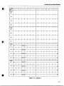
The 7704 uses six kinds of memory: 2K, 4K, and 8K ROMs and RAMs. The eight memory
sockets are designed to accept memory components compatible with the JEDEC 28 pin
standard pinout. Each socket can be individually configured for the 2K RAMs or any of the
ROMs. The 4K and 8K RAMs are the exception. The sockets can only be configured for
these in groups of four. The groups will consist either of sockets 0, 1, 2, and 3, or sockets 4,
5, 6, and 7.
o
After having chosen the memory combination best suited to your needs, as discussed in the
Memory Decoder section, the sockets should be configured accordingly. Figure2-22 shows
where to place the memory socket jumpers for each kind of memory. The location of these
jumpers is shown in Fig. 2-4. Jumpers W9, W10, W11, W12, W14, W15, W16 and W17
correspond to sockets 0 through 7 respectively. Jumpers W8 and W13 are used to configure
the sockets for 4K or 8K RAMs. Jumper W8 affects sockets 0, 1, 2, and 3, jumper W13
affects sockets 4, 5, 6, and 7.
Figure 2-23 is a list of pin compatible memory components for use on the 7704 card. The
recommended memory components are indicated by an asterisk. If you wish to use another
memory component, compare its data sheet to the socket configurations. Also, check the
data sheet for any special requirements, and be sure the parts are fast enough for the
processor you will be using.
Note: As of this writing, 4K and 8K byte-wide RAMs are not available and have not been
tested on the 7704. Any 4K or 8K by~e-wide RAM that conforms to the JEDEC 28 pin
standard and is fully static should be able to be used on the 7704. Pro-Log will be evaluating
some of these parts as they become available.
0
o
2-22
Installation and Specification
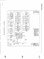
r- - - -
Wy - - ,
28
+5V
NOT
USED
A12
I
I
,
A7
26
Vee
A6
25
A5
24
7'
22
28
NOT
USED
A12
+5V
,
I
,
,
I
+5V I
0
I
1
,
27
I
,
I
I
A7
26
Vee
A8
A6
25
A8
r--WX---,
1 ,
,2
A9
A5
24
A9
I
A4
('3
RO'
A3-
22
RO'
I
L. -
-
-
-
-
-
-
-'
23
,,4
A3-
+5V
,
I
Wy - - ,
: WR*
+5V I
,
3
+5V : 0
1
27
r- - - -
,
: WR*
L. -
-
-
-
-
-
-
-'
0..-+ +5V
: All
A2
21
Al0
A2
21
Al0
Al
20
CE'
Al
20
CE'
AO
10
19
07
AO
10
19
07
DO
11
18
06
00
11
18
06
01
12
17
05
01
12
17
05
02
13
16
04
02
13
16
04
GNO
14
15
03
GNO
14
15
03
o.-+WR'
,6
L. ____5'
...J
4K EPROM/ROM CONFIGURATION
2K EPROM/ROM CONFIGURATION
r- - - -
+5V
A12
28
2
NOT
USED
+5V
,: WR*
,
I
27
A7
26
Vee
A6
25
A8
A5
24
A9
A4
23
A3-
22
A2
21
Al0
A1
20
CE'
0
1
WY -
-,
I
I
+5V I
,
3
,
I
,
I
L _ _ _ _ _ _ _ ...J
r--WX---,
1,
12
I
o.-f+5V
o--rAll
RO'
AO
10
19
07
00
11
18
06
01
12
17
05
02
13
16
04
GND
14
15
03
I
,WR'
,6
L. ____ 5'
...J
2K RAM CONFIGURATION
r- - - -
Wy - - ,
: WR*
+5V
28
+5V
A12
•
2
1
3
27~--~,--~
I
A12
I
,
+5V
26
+5V
A6
25
A8
r--WX--,
A5
24
A9
I
A4
23 ~--+-'-<l
A3
22
A2
21
Al0
Al
20
CE'
L. -
-
,2
_
-
_
-
_
-'
2
l'
o---;-+5V
I
I
All
I
o-fWR'
,6
L _____5,
.J
WY -
-
I
_ _ _ _ _ -'
25
A8
A5
24
A9
A4
231---+C"-<J
A3
22
A2
21
Al0
Al
20
CE'
AO
10
19
07
AO
10
19
07
11
18
06
DO
11
18
06
01
12
17
05
01
12
17
05
02
13
16
04
02
13
16
04
GNO
14
15
03
GNO' L...-_
14
_ _ _ 15
03
~
I
'
2 ~ +5V :
A6
RO'
-,
1
27,
,
26 +5V L. -
00
8K EPROM/ROM CONFIGURATION
,
:
A7
I
A7
RO'
+5V
+5V I'
,I 0
I
r- - - -
: WR*
I
'
r--WX--,
'2
l'
I
o---;-+5V
I
I
All
,
o-fWR'
16
L _____5.JI
8K or 4K RAM CONFIGURATION
(MUST BE
USED IN GROUPS OF FOUR)
Figure 2-22. Socket Configurations
2-23
. . . . .MI&J!iiIiWWIiiYi&!ii,MDiffiiiWGiMWlmiiiWiQJPlJli.iw411.JiilMhMiJd&L&t"GWWW;.hI.INi&iliGGWRl&14ii;ALdIi_&lli.aWAMYi&=i&&I'itNCiAMWiMt.a&li&lM. . .
MM;gMmw.. ;:; Ii; ¥f'IifIlI'\ i •• 41;=;;'." ,j
Installation and Specification
CHIP #
ORGANIZATION
ACCESS
218122K
2K SRAM
150
2716*
2K EPROM
350-650
2732*
4K EPROM
450-550
2732A*
4K EPROM
200-250
2764*
8K EPROM
200-250
MK34000
2K ROM
350
MK37000
8K ROM
300
MK2716*
2K EPROM
300
MK2764*
8K EPROM
450
MK4802
2K SRAM
o
INTEL CORPORATION
MOSTEK CORPORATION
NATIONAL SEMICONDUCTOR
MM2716*
2K EPROM
350-450
2K EPROM
250-450
MOTOROLA
MCM2716*
TEXAS INSTRUMENTS
TMS2516*
2K EPROM
MITSUBISHI
M58725*
2K SRAM
200
uPD2716*
2K EPROM
450
uPD2732*
4K EPROM
no spec
2K SRAM
200
2K EPROM
350-450
2K SRAM
150-200-250
2K SRAM
150-250
NEC MICROCOMPUTERS
AMERICAN MICROSYSTEMS (AMI)
S4028
SYNERTEK
SY2716*
OKI
MSM5128*
TOSHmA
TMM2016*
* Recom mended Devices
o~
Figure 2-23. Memory Components List
2-24
Installation and Specification
•
UNUSED SOCKETS
Aside from different memory types that can be used and the different combinations that can
be selected, further tailoring can be done to suit the 7704 card to your application. This can
be done by disabling any unused sockets.
Jumpers W7, 1-2 through 7-8, and W6, 7-8 through 1-2, correspond to sockets 0-7
respectively.
When a socket is disabled, the chip select signal is disconnected from the socket. Also the
data bus buffer no longer responds to memory requests in the address range of the unused
socket. This means that memory on other cards in the system can occupy this address space,
without interference from the 7704 card.
Any number and combination of sockets may be disabled. By this method, the 7704 card can
be configured to occupy as little as 2K of memory space. These 2K blocks may occupy
adjacent address fields or be widely separated. They may be mapped anywhere within a f)4K
memory system on the natural 2K boundaries.
MEMEX
The function and operation of the MEMEX will be explained in Section 3. This section is to
explain the jumper options affecting MEMEX.
o
On the 7704 card, MEMEX can be used in one of two ways. The first method is to use the
MEMEX line to enable the card. Using this method, two 7704's can occupy the same address
field, only one of which is enabled at a time depending on the logic state of the MEMEX line.
The second method seperates the memory on the 7704 into two banks. Only one half of the
card is enabled at a time. Therefore, both halves can occupy the same address field.
As shipped, the card employs the first method. The 7704 card is enabled when MEMEX is
low. To reverse its polarity, remove jumper W2 from position 1-2 and replace it with one at
position 3-4. The location of this jumper is shown in Fig. 2-4. When using two of these cards
which a.re both g'oin~ to occupy the same address field, one must have its polarity changed.
It is important to ensure that the MEMEX line is not left floating.
The line must be either
controlled by some other card in the system, or tied to ground on the 7704 itself. Pro-Log
processor cards either control the MEMEX line or simply tie it to ground. If there is no card
in the system controlling MEMEX, or if you wa.nt the card to disregard MEMEX, jumper Wl
can be removed from position 3-4 and be replaced by one at position 1-2. This will tie the
line to ground a.nd permanently enable the card.
If MEMEX will be used to divide the 7704 into two banks, jumper Wl should be in position 1-2
to permanently enable the card. Also, jumper W4 should be in position 3-4.
•
Jumper W4 serves two purposes. It is part of the Memory Decoder Control jumpers. A
jumper in position 1-2 serves as a low level input to the Memory Decoder. With no jumper
installed it is a high level input. A jumper in position 3-4 connects the MEMEX line to the
Memory Decoder input. Therefore, by changing the state of the MEMEX line, you can select
a different Memory Decoder option. This is not something you would want to do with most of
the options. However, with options 6A and 6B it can be done. Option 6A only uses sockets 03. Option 6B only uses sockets 4-7. Both options use the same memory address field .
Therefore, by controlling the MEMEX line, you can select one of two memory banks on the
7704 card.
2-25
. " " " . . . . - '. .'.,tiiQAMQJMiM,mWMI#A
,,4'., . , "';;.4U;;;
41
i
4,.',."
:
MAR
;;rot¥4Aqp
4 $.
£Ad4& #.4.4 fl..
Installation and Specification
Segment Select
The function and operation of the Segment Select line will be explained in Section 3. This
section is to explain the jumper options affecting Segment Select.
o
The Segment Select line is not a part of the STD BUS. It is an external line which must be
connected on the card ejector side of the 7704, when it is used. Figure 2-2, shows the
location of the connector.
The connector type is a 2-pin 0.1 inch center connector. The cable should be a twisted pair,
consisting of one signal line and one ground line for added noise immunity. Figure 2-26
shows which pin is signal and which is ground.
An I/O card, such as Pro-Log's 7605 card, along with an RC704 cable can be used to control
the line. One output bit, or line, per 7704 card is required. Therefore, one output port can
control eight 7704 cards.
As shipped the card is enabled when the Segment Select line is in the high state. Its polarity
can be reversed by removing jumper W3 from position 1-2 and replacing it with one at
position 3-4. See Fig. 2-4.
With jumper W3 in position 1-2, the Segment Select line can be left unconnected. A pull-up
resistor on the line will hold it in the active condition. If jumper W3 is in position 3-4
however, the line must be controlled in some manner, or the card will remain permanently
disabled.
Specifications
Figures 2-24 and 2-25 are electrical and environmental specifications. Figures 2-26 and 2-27
describe the specifications for the interface connections and card edge connections.
Figures 2-28 through 2-33 are the timing requirements necessary for the 7704.
Recommended Operating Limits
o
Absolute Non-Operating Limits
Mnem.
Parameter
Min.
Typ.
Max.
Min.
Max.
Units
Vee
Supply Voltage
4.65
5.00
5.35
0
7.00
Volts
-
Free Air Temp.
0
+25
+55
-40
+75
°C
-
Non-Condensing
Relative Humidity
5
95
5
95
%RH
O~
Figure 2-24. Electrical and Environmental Specifications
2-26
Installation and Specification
•
Mnem.
Icc
Parameter
Max
Typ.
Min.
Vee Supply Current
Units
500*
MilliAmp
·With memory sockets empty
Figure 2-25. Electrical Characteristics
PIN NUMBER
OUTPUT (LSTTL DRIVE)
INPUT (LSTTL LOADS)
MNEMONIC
I
SEGMENT 0*
5
I
PIN NUMBER
OUTPUT (DRIVE)
INPUT (LSTTL LOADS)
MNEMONIC
GROUND
r
2
1
1
~ND
• Active low-level logic
Figure 2-26. Interface Specifications
PIN NUMBER
OUTPUT (LSTTL DRIVE)
INPUT (LSTTL LOADS)
INPUT (LSTTL LOADS)
MNEMONIC
VCC
2
1
VCC
GROUND
GND
4
3
GND
6
5
+5 VOLTS
GROUND
-5V
D7
1
55
8
7
55
1
D3
D6
1
55
10
9
55
1
D2
D5
1
55
12
11
55
1
D1
D4
1
55
14
13
55
1
DO
A15
1
16
15
1
A7
A14
1
18
17
1
A6
A13
1
20
19
1
A5
A12
1
22
21
1
A4
A3
A11
1
24
13
1
A10
1
26
25
1
A2
A9
1
28
27
1
A1
A8
1
30
29
1
AO
RD*
1
32
31
1
WR*
MEMRO*
1
34
33
IORO*
MEMEX*
1
36
35
IOEXP*
MCSYNC*
38
37
REFRESH*
STATUS 0*
40
39
STATUS 1*
BUSRO*
42
41
BUSAK*
INTRO*
44
43
INTAK*
NMIRO*
46
45
WAITRO*
PBRESET*
48
47
SYSRESET*
CNTRL*
50
49
CLOCK*
PC1
•
OUTPUT (DRIVE)
MNEMONIC
+5 VOLTS
-5V
o
PIN NUMBER
IN
52
51
AUX GND
54
53
OUT
AUX GND
PCO
AUX-V
56
55
AUX+V
• Active low-level logic
Figure 2-2'1. Edge Connector Pin List
2-27
_m-=ua:a'A,;iUWWi4XiWiiUd:". i #i ,. I\h
,:
t, M1 iff#
NT '#fA #4
;;¥
Installation and Specification
o
STD BUS
ADDRESS
ON CARD
ADDRESS
: 1i ----..~
===2f=t==tAD==================
tCS
CHIP SELECT
CEO* - CE7*
\
1/
14
tAC
tAD
tCS
tDV
tWR
I'...
......
tAC2
VALID DATA
~
--..
ON CARD
BWR*
SYMBOL
.1
tDV
ON CARD
DATA BUS
STD BUS
WR*
-4-tWR
~'
NANOSECONDS
MIN.
TYP.
MAX.
PARAMETER
7704 minimum safe write cycle time
Addreses buffer delay time (STD Bus to memory socket)
Chip select logic time (STD Bus to memory socket)
Chip select to data valid time (STD Bus to memory socket)
Write buffer delay (STD Bus to memory socket)
220
18
4!;>
74
12
30
70
112
18
All above times are assuming that WR*, MEMRQ*,MEMEX and SEGMENT are true prior
to STD BUS address becoming true.
0
A memory device with an access time equal to tDV was used here. A memory device
faster than tDV will not improve the access time of the card.
To find write access time of the 7704 with a specific memory device of longer than
112 nsec access time use the following equations.
tWA
=tAC - tDV + tAA
tWA> tAC
Where:
tW A =Total access time of card and memory device for write.
tAC = 7704 minimum safe write cycle time.
=7704 chip select till data valid at memory chips.
tAA =Memory device access time.
tDV
If device access time (tAA) is less than or equal to 112 nsec then tAC is the total access
time (200 nsec).
* LOW LEVEL ACTIVE
Figure 2-28. 7704 Timing for Write
2-28
o
Installation and Specification
•
;r_I_~_t_AD
STD BUS
ADDRESS
___
ON CARD
ADDRESS
CHIP SELECT
CEO* - CE7*
_ _ _ _ _ _ _ _ _ _ _ _ _ _ _ _ _ __ _
I
~ tCS---~~1
~--tM ---~.KOD :+-
ON CARD
DATA
144---------------tAC1
STD BUS
DATA
o
--------------~·~----D-A-TA--V-A-L-ID---
PARAMETER
SYMBOL
tAC
tAD
tCS
tOO
tM
_____________________________
Minimum safe access time for read
Address buffer time delay
Chip select logic time
Data bus buffer time delay
Data buffer enable time
NANOSECONDS
MAX
MIN
TYP
220
18
45
8
64
30
70
12
100
All above times are assuming that RD*, MEMRQ*, MEMEX and SEGMENT are active priorto STD BUS address
becoming true.
Figure 2-29. 7704 Timing for Read
STD MEMEX
CHIP SELECT
CEO*-CE7
SYMBOL
TMX
•
PARAMETER
Time MEMEX valid to chip select*
NANOSECONDS
TYP
MAX
77
118
The above parameter true if all other signals are active prior to MEMEX going active.
Figure 2-30. 7704 MEMEX Timing
2-29
Installation and Specification
SEGMENT*
AT CONNECTOR
~-------tSG1------~~~1______________-------------
READ/WRITE
BUFFER OUTPUT
o
~-----------tSG2----------------~·:1
DATA BUS DRIVER
ENABLED FOR WR ITE
DATA BUS DRIVER
ENABLED FOR READ
SYMBOL
tSG1
tSG2
tSG3
----~------------------------~~.<~--------
I~I~~----------- tSG3------------------~~I:
------------------------------~.<~---NANOSECONDS
MAX
TYP
PARAMETER
SEGMENT* valid to RD* + WR* buffer output valid
SEGMENT* valid to data bus driver enabled for write
SEGMENT* valid to data bus driver enabled for read
54
75
81
82
114
122
The above parameters are true if all other signals are active prior to Segment* going active.
Figure 2-31. 7704 Segments Timing
o
STD
MEMRQ*
READ/WRITE
BUFFER OUTPUT
DATA BUS DRIVER
ENABLED FOR WRITE
DATA BUS DRIVER
ENABLED FOR READ
SYMBOL
tMD1
tMD2
tMD3
t
I~
~
tMD1
tMD2
~
~K
~I<
tMD3
NANOSECONDS
MAX
TYP
PARAMETER
Time MEMRQ* to RD* + WR* buffer enabled
Time MEMRQ* to data bus driver enabled for write
Time MEMRQ* to data bus driver enabled for read
46
67
73
Above parameters valid if all other signals are active prior to MEMRQ* going active.
Figure 2-32. 7704 Segments MEMRQ*
2-30
------
-----------------
70
102
110
o
Installation and Specification
•
STO
RO* OR WR*
ON CARD
BRD* OR BWR*
SYMBOL
tRW
PARAMETER
Time RO* or WR* till BRO* or BWR* on 7704 card
NANOSECONDS
TYP
I MAX
12
Above parameter valid if all other signals are active prior to RO* or WR* changing state.
o
I
18
Figure 2-33. 7704 RD* or WR * Timing
•
2-31
()
o
o
2-32
SECTION 3
•
Operation and Programming
This section describes the functions and use of the 7704 card. The card is designed to be a
versatile part of your memory system.
It can be used in both small and large scale applications.
By using the memory size and
mapping options described in Section 2 and the MEMEX and Segment Select lines described in
this section, the 7704 can fill the memory requirements of virtually any system.
MEMEX
The MEMEX line is a part of the STD BUS. It is used as a memory bank select line. Using
this line allows two banks of memory to occupy the same address field. Only one of the banks
is selected at a time, depending on the logic state of the MElVIRX line.
It is normally controlled by a memory segment controller, or an output port.
The segment
controller or output port can be either on the processor card, or on some other card in the
system. Some Pro-Log processor cards have an onboard output port for controlling MEMEX.
MEMEX Example
o
An example of how MEMEX can be used is shown in Fig. 3-1. It shows a 124K memory
system. It is comprised of 4K of RAM and 120K of ROM. The RAM is on the processor card
and is permanently enabled. That is, it ignores MEMEX. The ROM is in two 60K banks, one
bank on each 7704 card. Only one card is enabled at a time dash the one on the left when
ME MEX is low, and the one on the right when it is high.
At power up, the MEMEX port is low. The Primary memory bank is therefore enabled. The
processor can then choose Primary or Expanded memory simply by manipulating the MEMEX
line.
A second example is shown in Fig. 3-2. In this example the two memory banks both reside on
one 7704 card. The system has 96K of memory, consisting of 64K ROM and 32K RAM. The
64K ROM is in two banks of 32K each. The RAM is on two 16K RAM cards, and is
permanently enabled.
At power up, the MEMEX port is low. Primary memory is therefore enabled. Again, the
processor can choose between Primary and Expanded memory simply by manipulating the
MEMEX line •
•
3-1
_ _ _ _."""'.MmW1&l,. . . . . .G'. . il'-C,IQltMI.4bUillMMtiAigX ; It"',
; $I $
AP; NIIN :
,MA
T4TiAl4MA4q
4. q
444#44
Operation and Programming
o
o
W
et
-.:to
oZ
..... et
..... Q.
><
W
:E
o
a::
o
~
CD
It
LL.
"t
0
0
g
o
>-
oen
~
o
eta:
0:E
a::
"t
o
0
0
-.:tet
-
..... a::
.....
Q.
a:
It
o LL.
:E
CD
g
en
W
o
a::
Q.
Figure 3-1. 7704 MEMEX Example
3-2
_ .. _ - - - - - - - - - - - - - - - - - - - - - - - - - - - - - - - - - -
o
Operation and Programming
•
C
0:
C
0:
<t
0
:E
<t
0:
~
iL
iL
iL
iL
I
0
0
0
<t
0
iL
iL
iL
iL
I
0
0
0
:E
<t
0:
co
~
CD
.,...
co
.,...
CD
o
0:
o
en
en
w
o
o
0:
I:L
•
Figure 3-2. 7704 MEMEX Example
3-3
i_AtwA£MJiiki*,U"';;;;;;; 'Aii.·; , ;;,
caUl'""
Ii
d"
I
$",
,.
,w'::
WC"
Operation and Programming
MEMEX Control Software
The software for controlling MEMEX requires some special consideration.
taken to avoid confusion when changing memory banks.
Care must be
o
There are a number of ways to deal with this. What follows are a few examples.
MEMEX Control Software Example One
In many systems using MEMEX, it will be advantageous to keep some section of memory
permanently enabled, a section wh1Ch---dis~egards MEMEX. This may be a section of ROM
memory at the low order addresses, or a section of RAM used to store registers, program
variables, and the stack, or a section of ROM containing interrupt service routines that need
to be quickly accessible at all times.
If your system will have a permanently enabled section of memory, the MEMEX Control
software can reside in this section. If the section is RO M, the program would simply reside in
the ROM. If the section is RAM, the processor could load the program into the RAM. The
program would be stored in ROM, disc, or some other nonvolatile memory. The processor
would load the program into RAM as part of the power-up intialization process.
Using the system in Fig. 3-1 as a model, a program could be written like the one shown in Fig.
3-3. It assumes you are jumping from a main program in one bank to a subroutine in the other
bank. The address of the subroutine you are jumping to must be in the HL register pair. The
program selects the proper memory bank and jumps to the subroutine. When the subroutine is
exited, the processor returns to the MEMEX control program. The program reselects the
original bank, then returns to the program from which it came.
0
Fig. 3-3 shows two programs. One to jump to a subroutine in Expanded memory, and one to
jump to a subroutine in Primary memory.
o
3-4
Operation and Programming
•
HEXADECIMAL
MNEMONIC
INSTR.
1
MODIFIER
COMMENTS
01
oPA.
5
I..
7
E:f
f-I.L
HL
,. .\L
A
3£
Llt4l:.
co
c 1>3
..00
B
c
E
I~
CA
I~
F
00
1
2
u"3
I
f~
00
~PA
0
1PtJ
A ;'::;
B Qi
c
D1
E
Cq
F
•
Figure 3-3. 7704 MEMEX Software Example One
3-5
_Wii&#&I&Ua&liGW11WIMdi.=W!GMIR&Q( MMrlU!£"G =lI· ibA q, 1U.,.YlbIQ Ii _;
Operation and Programming
MEMEX Control Software Example Two
In the first example it was assumed that anytime the program jumped from one ba.nk to the
other it was to jump to a subroutine. Fig. 3-4 is a program for jumping from one bank to the
other, but not as a subroutine.
o
The program simply changes the state of the MEMEX line, and then jumps to the address in
the HL register pair. Again the program is divided up into two sections dash one to go from
Primary to Expapded memory, and one to do the opposite.
HEXADECIMAL
~~E
yr
~~:
INSTR.
f!o '31::
1
2
TITLE M~(':l
MNEMONIC
LABEL
'Tn
nl
Ex"
~'3
INSTR.
CPA-
Eti
I'H
l5<2.
DATE
COMMENTS
~
LllAr:
••
C:F.'7"~~ U-.t.f.4
i.i~III..."
"'
5~cr
r:vOAa~
.~
3>Oc.
4
~lJ~WA1L~
MODIFIER
U.T
I~
R»2:r .. AA.'\ PO.-,.
n A-akll'H ,Ll
~
1m
lUNP
'~
I-lL
,
5
.
'~
7
8
1"h
p~
'"
M'"
9
~
A
/"X)
B
b3
.OiA
c 1",,,,D "81
~P&1·
-
!
~
."<
.
'5~ A'l~
-- .. "
....
~
~..:rUM'
In
n
1.zJM/
5:'~r
~''T"' 1M'a"~
AIJI'JflA.( IN'
U.,
A~
-
o
PA-tL
E
F
0
1
2
fo-
3
4
5
..
7
8
9
A
B
C
D
E
F
o
Figure 3-4 7704. MEMEX Software Example Two
3-6
Operation and Programming
•
MEMEX Control Software Example Three
So far we have looked at ME MEX control software residing in a section of memory which is
permanently enabled. Figures 3-5 and 3-6 show how the control software can reside in
memory that is affected by MEMEX.
Figure 3-5 shows how a program can be written to jump from a program in Primary memory
to a subroutine in Expanded memory. Note that both sections of the program reside at the
same addresses. However, one part is in Primary memory and one part is in Expanded
memory.
Figure 3-6 shows how the program looks to the processor.
coherent program.
When it is run, it becomes one
This program only allows for jumping from Primary memory to a subroutine in Expanded
memory and then returning. In normal operation you would probably also want one to do the
opposite.
To use the program, you must be in Primary memory. When you want to jump to a subroutine
in Expanded memory, you load the address of the subroutine into the HL register pair. Then
perform a Jump to Subroutine to the MEMEX control program. The program will direct the
processor to change memory banks and jump to the subroutine. After running the subroutine,
the processor will return to your original program.
c
HEXADECIMAL
P:~E
If f
~~~
Fo
1
MNEMONIC
INSTR.
3f
01
-
TiTlE
LnA1:.
rv
~()
NO'
~
8
(-.,I)
tJoP
tJoP
No(>
K
1'\0
9
Do
00
(')(7A
NOt'
l-
l2
'-lei'
:z
NoP
I1t
M
NAP
()()
~oP
~~
(l...,.$
I--
lV)P
-m
~o
DO
1
fill
2
00
300
4
z::5
5
tl
6
~A
7
':'i=
8
~3
9 £1
Ai
B
3£
00
c b3
D
E
F
-
-
"IoePf
J'N
~
-
nil;.
AOOit£~~
UNuSeD
,
EX.rr
IlNulro
~
'-'L
loll
>-
~/JJH
2:
fl .... n
leruttJ AOotc;'~
[ ~~FA)
<;nkl..
~
I:H.
..Ji!L00
"'
Q
r
L-
-11\10441 1\
~~1U,11&
~~.""P -rI m.M~
~
.vi"
I·HL
Mr':M1l1t1.f
'1\
2
0
r.Jof
'POt{"
"'0
LDAL"
){,'J(.
00
0
Nfl
__ JJJJL
NtR
NI)'
'rSf'
LDrr
I.. ~
...
:z
B
m
6.PAtJ{) M.€:f\J.IJI.Y
7U
c
D
E
F
DATE
~
\~
8
"1\.1MP To
f--
01
EX.~
COMMENTS
~'/...
co
1[6\i-)( Sof1'wM€
MODIFIER
3
4
5
A
•
INSTR.
2
7C\r)
J:=~
LABEL
:<
-
~
,
4-- volli'"
M>O/U SS
lJlJu!.@
Figure 3-5. 7704 MEMEX Software Example Three
3-7
iUMWM_. . ." _ _.......mW.MWAfJiJ4CilG&&JlMti
Operation and Programming
o
HEXADECIMAL
E
INSTR.
'::o"R
~~~
F='f IF
0
1
2
3£
MNEMONIC
LABEL
INSTR.
-
f)-;
'1...'1--
f'lPA
3
4
e.t5
PSf'
LC>P:C
5
1..t
6
FA
7
9
FF
E;:'
'E:G
A
:3f:
B
co
c
b~
8
0
X:J..
E
c.q
Ol
)(CPr
~PN
.
.~
HL
0-;.;..
J.\L
rn
~.
HL
Ht
LbAI.
-
olA
-
Rrs
F
00
ME14o!.lf
~PInJO
'~
I
.1o!:....J
--
DATE
COMMENTS
r.:;-, ., .:fUI\1' 1b
LbAI
()(
£,,-3
KUNJJINb
TITLE
MODIFIER
~
- -:( AOOWSS
ruSh
~ttJ M>Ot€H O"'f"o
.,
';
.. -1c1~# "fh
-i,
• ...f, 'MoO 1i
..c
-'iii
::r:ar
:s~ (FF'FA
c.." ", ,....
C
fl1.llkt\-£"f
Ar
H.l
WI ~ 11£ \f
~~POtl:r AODiE'SS
~rr"'
0
1
2
3
4
5
6
o
7
8
9
A
B
.C
D
E
F
Figure 3-6. 7704 Running Example Three
MEMEX Control Software Example Four
The example shown in Fig. 3-7 is similar to the last example. In this one however, rather
than jumping from one bank to another as a subroutine, this program performs a simple jump.
This program is in two sections. One to go from Primary to Expanded memory, and one to do
the opposi teo
Fig. 3-8 shows how the programs looks to the processor. To the processor, either program
appears to be one coherent program.
To use the program, load the address of the program you want to jump to into the HL register
pair. Then jump to the MEMEX control program. The processor is directed to change memory
banks, then jump to the program you requested.
3-8
0
Operation and Programming
e
HEXADECIMAL
P:~RE
Ff
~~:
INSTR.
~O
o€.
1
2
QI
-",-7;
3
¥.i
4
MNEMONIC
LABEL
To f!!:t.SI
INSTR
TinE
LI>A'!
-
·8
·c
F~
A
-rh f'IZ:I:'
MOP
~
~oP
~
I~
IH
-ro
i==-O
('()
AIM
I--
1
I'In
tJOP
m
200
tJnP
X
3M
IIInP
['Q
r;.."1.1
1P11
~q
UI
5
•
I ....L _
~
~
_~(a...
11'.... " '""
,u
J.I
III
a I-z,E
no
10 ttl:
b"'>
B '/.'1..
A
WlA'!
()PA
-
n
PIlIMM.'1
Mc1401.V
~
~
..-
Iz
HDP
(')0
11lM~
'C'I
no
l'Dt'I
jrOhe~
1I1l,,~(n
~.
k
t------I-. D
E
L-.-.•
LJI
I,)
~
7
c
AMu- «
n
1,1II1II 0
~
~
E
9
/' ....1.."',..
iO
F
4
AftNJ~(
I/""c~/\
k-
:D
'::'f'
tAP.... ".tI
~
~
~
IIlll1'
MOP
IPN
+- ~"'1"
JO
I-
7
00
N'"I
rY'-I
-n r:... ,.,flt:ft
,I
~
NoP
5
9
-1:
I--
•
a (}{)
DATE
COMMENTS
01
Drl-.
DO
~··1II/~F"t'4
NMfi
MODIFIER
I--
--!_'--_ L..
Figure 3-7. 7704 MEMEX Software Example Four
o
HEXADECIMAL
'::~E
~~~
Ce:
~O
INSTR.
2
13~
1)(
h-a,
3
>LJ
4
~
1
MNEIIIONIC
,0
LABel
ff:I.J
INSTR.
nnE
-
()I
DATE
COMMENTS
Mf&.AOt.V
::rUM' 11 l::lliAN OE1l
~
:~
'I
f'lPA
1'PtJ
Ei~
Qulllln't..
MODIFIER
IL\)A"!:
i=-I
UL
It
f{Jl:(
I- :;
1VM"
ItMIJiii.<.
-'Tn ~
,.
5
,J
~L
11ft
•
7
83~
9 r.()
A
b~
B
'If'L
c £q
"it! PIl.t.
1.
L-bAr.
-
00
j'1'N
Hl
OrA
-
-
';1.
D
~
E
l~
F
•
jllMf
-n
I~
VTi''f
.iUMP
"'-.MIW·\
.,A_of.....,
A1>0ti?. ~
-n
AOIlf",~\
,..I
"'
t=-'
0
1
2
3
4
5
8
7
a
I
A
..
C
•
D
!i-
F
Figure 3-8. 7704 Running Example Four
3-9
mill(
.-
Operation and Programming
MEMEX Interrupt Control Software
This last example shows how interrupt service can be handled in a system using MEMEX.
o
One method previously mentioned is to set aside an area of memory for interrupt service.
This area would be permanently enabled.
A second method can be used if the interrupt service routines are short enough. This method
has identical service routines in both Primary and Expanded memory. Both routines would
reside at the same addresses. This method may, however, use up too much memory space.
A third method is shown in Fig. 3-9, 3-10, and 3-11. In this method, the service routines
reside in only one bank of memory. In the example shown, they reside in Primary memory.
The function of the program is to coordinate the jumping to and returning from the interrupt
routine. The program ensures that the processor gets to the service routine. If the processor
is in Expanded memory, it directs it to switch to Primary memory. It also ensures that the
processor returns to the correct bank, after the interrupt is ·serviced.
The routine resides at address 0024. This is the address an 8085 processor jumps to when it
receives a non-maskable interrupt.
Follow the flow chart in Fig. 3-9 and assume that the processor is in Expanded memory when
it is interrupted. The processor is directed to select primary memory. It does this by
clearing the MEMEX bit in the accumulator and writing it out to the MEMEX port. In
Primary memory the processor complem'ents and stores the MEMEX bit. After the interrupt
is serviced the MEMEX bit is retrieved. When the bit is output to the MEMEX port, the
processor is returned to Expanded memory. It then returns to the program from which it was
interrupted.
0
If the processor is in Primary memory when it is interrupted, it sets the MEMEX bit in the
accumulator to a one. It is then complemented and stored. After the interrupt is serviced,
the MEMEX bit is retrieved and is output to the MEMEX port. The MEMEX line is already
low, however, so this has no effect. The processor simply continues in Primary memory. It
then returns to the program from which it was interrupted.
Figures 3-10 and 3-11 show how this program could be written. The program in Fig. 3-10
would reside in Primary memory, and the program in Fig. 3-11 in Expanded memory. This
program should reside at each address where an interrupt service routine is located.
o
3-10
Operation and Programming
•
HEXADECIMAL
P:~AE
~~:
Db t
MNEMONIC
INSTR.
LABEL
INSTR.
nTlE
+ COMMENTS
'NrER.
H~ME'i.
MODIFIER
DATE
f0o-
0
l
2
3
1
4
5
I
~E
0'
I(MfN.K ... II...-ra)
-
~o,
I
1.1=
l!.... A
9
F'i
P~i'
Al=
A
{.:}
11
UN
~
I)J~R
l-
M=
~
-S,
c (')(\
F
FI
IJ:"J
'/...'/...
30
leG
1
)('L
2
X'J...
'Y- i.
E
3
4
5
X,L
JC.ll
I
)(~
7
'1...'"
I
)(
9
x.'J..
X. 1.
A
B
c
t;~ 1utF='.... ~
T
(1--" ,.... e.ff'"
1M
ACLLlMLlL...A.:toil.
sr"aL'
M6.t~ i'.11'"
Ill"'"
tJnP
nl'l
00
D
,.
.v
0/
7
B
Of')
LDA'(
E'l..rr-
PLP
S"-JP
T
f1v(!:{L
I1Q
t
..,.
~et"R.IFNl!.
Oi1A.
I"
~
if 4&--
K.~
I.,
8.11"
-
~
INT~1l
A1.IO
<b
r""
f:i'1"
Tb
AoJO Dvnvr"
IIIIT'E'i.
M~~
eo ••
-D~o~A.41I\I1~<{,
Me:Mo~Y
UIlIMIrt.'4
Iool~ D IP~
13
Ii"
I'
Sawl"::
~
~"
*'1..
D
If,"",
E
l..b
iF
'f
-
Foo
,.
UN
,
be
C1.,-r-
I
~,1""
I--
Figure 3-9. MEMEX, Interrupt Software, Primary Memory
o
~~:
C!.l'l
10
INSTR.
nTlE Mt=:M~'
MNEMONIC
HEXADECIMAL
P~G"E
LABEL
INSTR.
MODIFIER
1
2
-I-
1t..I'I'l"'fl..
DATE
COMMENTS
-
3
14
5
3~
1'\(\
I
l'I~
7
}(J..
( Uhlllflff.4"IAI1I'II\
CJ.!At. ,,",,0 O"'-PI&1" MeN\e:1.. all':
Mi:MoA..'i
~l!ui.l"!o ~il.IMJ'\oI.'t
Lb6.1:
-.
~ll
0160
n. __
MlDR.~K
It"lI"I
pJl\O
I'"
9
nl\
f\J6~
1m
A
1'10
NO'
')(
B
ab
filM
c
fYoo
IIIn'
D
Ot'l
NIU
:a:.
E
00
NOI
17
F
00
NoP
8
U:"
rtf'S
~o
1
IC""I\~
..
~
Ir
an" (""'.,,, .... "''''''' lUP.Ntlf\4)
::t.
2
l\\
3
~
,.
4
5
0
I
..(.
7
I
9
A
B
C
•
D
E
F
t-
Figure 3-10. 7704, MEMEX, Interrupt Software Expanded Memory
3-11.
_=iMJ&&Ji&WI4\lQiiAhl Mti¥li;;;; iX
,«;;,
/TM4!M.$M#4PiMAM 14AW;
Operation and Programming
o
PRIMARY
EXPANDED
SET MEMEX BIT
IN
ACCUMULATOR
CLEAR MEMEX
BITIN
ACCUMULATOR
1+-4--8
COMPLEMENT
AND STORE
MEMEX BIT
OUTPUT MEMEX
BITTO MEMEX
PORT
RETRIEVE
MEMEX BIT
o
OUTPUT MEMEX
BITTO MEMEX
PORT
SERVICE
INTERRUPT
o
Figure 3-11.7704, MEMEX, Interrupt Software Flowchart
3-12
Operation and Programming
•
Segment Select
The Segment Select line is not 8. part of the STD BUS but is an external line which must he
connected on the card ejector side of the 7704 when used. Fig. 2-2 shows the location of the
connector. The purpose of the line is to allow the 7704 card to participate in large scale
memory bank select schemes where multiple cards occupy the same address field.
Whereas the MEMEX line can be used to select one of two banks of memory, the Segment
Select line can choose one of any number of memory banks.
The line is normally controlled by a. memory segment controller or by output ports. An I/O
card such as Pro-Log's 7605 card along with an RC704 cable can be used to control the line.
One output port can control eight cards.
Figure 3-12 is an example of how the line can be used. It shows a. 184K memory system with
4K RAM and 180K ROM. The 4K RAM is on the processor card and is permanently enabled.
The 180K ROM is on three cards. Each card has its Segment Select line connected to a bit of
an output port on an I/O card. All three cards occupy the same address field.
A t power up the output port bits would be low. One of the 7704 cards would be configured
for low level active Segment Select. The other two would be high level active. Therefore,
one of the cards would automatically be selected at power up. The processor could
thereafter choose which card it wanted simply by writing to the output port.
c
A second example shows how MEMEX and Segment Select can be combined. Normally,
MEMEX will be used if possible, since it requires no additional lines. If Segment Select is
used, MEMEX would prohably not be used. However, they can be used together.
In Fig. 3-13, and 84K system is shown. It has 12K of ROM and 2K of RAM on the processor
card. This memory is permanently enabled, and could hold the main program, including
software for controlling MEMEX and Segment Select.
The rest of the memory is in four banks on two 7704 cards. Each bank uses approximately
the same address space. Note that each bank has a different combination of ROM and RAM.
Each bank could be dedicated to a specific job that the processor has to do. For instance, in
an interrupt system, the processor could use a different bank to service each interrupt. The
memory combination of each bank could be tailored to suit the specific job that it will be
used for.
The processor card is a Pro-Log 7804 card. It has one output line whi.ch is used here for
Segment Select. This one Segment Select line is connected to both 7704 cards. The one
marked Segment One is enabled when Segment Select is low. The one marked Segment Two
is enabled when Segment Select is high.
On the card marked Segment One, one bank is enabled when MEMEX is low, and one when it
is high. The same is true for the card marked Segment Two. The processor selects one
segment, or card by setting the Segment Select line high or low. It then selects which of the
banks on the card is enabled by setting the MEMEX line high or low .
•
3-13
_iiWiWJJ.-=-aIiAWi&W&AlMkC:tmdAA;;r:"U4$"M;« .... in ; ; ;,
«:W44:a
,:
t
;%M ¥¥AP4¥
Operation and Programming
:e
o
a:
~
o
CD
IL
IL
IL
W
I
o
o
o
o
....
N
....
0
....
a:
0
G.
N
....
Z
w
:e
e"
w
en
:e
0
a:
IL
IL
IL
w
I
0
CD
0
0
0
0
:e
IL
IL
IL
a:
W
~
....
....Z
w
:e
e"
w
en
o
~
o
CD
I
o
o
o
o
C
a:
<C
0
0
::::::
0
a:
en
o
en
w
o
o
a:
G.
o
Figure 3-12. 7704 Segment Select Example One
3-14
•
7704 SEGMENT 1
~
~.
CD
W
~
.
~
~
...::I
=
•
o
Primary
8KROM
40005FFF
6KRAM
600077FF
Expanded
16K ROM
40007FFF
4KRAM
80008FFF
7704 SEGMENT 2
Primary
24K ROM
40004FFF
2KRAM
AOOOA7FF
Expanded
4KROM
40004FFF
6KRAM
500067FF
~
00
~
9
a
~
s3
~
i
PROCESSOR ONBOARD
12K ROM
00002FFF
2KRAM
300037FF
ONE BIT PORT
o
1.....,...
g
[
...
."
t
W
I
~
CJ1
9
9
5'
aq
Operation and Programming
Segment Select Control Software
The control software for Segment Select is very similar to that used for MEMEX. The
difference is, that it must be able to control more than two Segments. To do this, the
program must be told what Segment to jump to. It must also be toId what Segment to return
to.
o
As with MEMEX, many applications will require an area of Permanent memory. The simplest
Segment Control software would reside in this area. Figure 3-14 is an example of such a
program.
It is similar to the program in lVIEMEX Software Example One. It coordinates jumping from
one Segment to a subroutine in another Segment. The difference here is that you must enter
the program with two additional variables. Register A must have the number of the Segment
you are jumping to. Register B must have the number of the Segment you are jumping from.
The "number" of the segment would be either 01, 02, 04, 08, 10, 20, 40, or 80 HEX. One bit
for each segment. This program can therefore control up to eight segments.
Any of the MEMEX control software examples can be adapted for Segment Control. Or
entirely different control software can be written. Use these as examples from which to
write your own programs.
HEXADECIMAL
P:~E
If1=-
'i~:
F
INSTR.
0
D3
1
2
'/.}(,
3
eli
MNEMONIC
LABEL
INSTR.
-
e 11
5
•
•
IU
-
PI!
7~
fF
14L
LbPr
-
F'I
Xc.PT
.~rN
UL
PLP
gc.
It.
LI
"1S
LoA.
&
B
))~
OPA
c
1..)(,
D
C,q
-
Ri~
E
F
0
1
2
3
•
.
o
DATE
VOitT
~51bf1J
SiaMWj"
Aft.i>ecrss:
SPrtlE O~t..Ir.1ArL. ~"""e'U1"" NLllVlloert..
Pout ll..I:t-ruL.J AtOa.ze:;.s.
(fFFCf)
I:lNTo
nP
or:"
-Sma.
,
UL
~Cj
P.9
Sw IrcH ,.,.
T
iF ...--
lie.
PS P
PSP
e,tWr~L.
COMMENTS
r--
OPA
CS
j£'rlElil
nTLE
MODIFIER
ir
""Q
11lMI n
~rt1'\lbJ
$.)U.Ou n~
1b
",I).
A"T"
,All
M.L
St!t.Mc::'IVI""
~
2
i
...
~
tr~l'O'l:( AObilG<;S
G~I1'
,
\
1
"'
4
1;1':
I~
5
-<..
8
7
•
9
It.
B
C
D
E
F
1-
Figure 3-14. 7704 Segment Control Software
3-16
o
SECTION 4
o
Operating Software
Section 4 is usually reserved for software for operation of an STD Series 7000 card. The 7704
card requires no software except for those examples given in Section 3.
•
4-1
o
o
o
4-2
SECTION 5
•
Maintenance
Reference Drawings
The schematic (Fig. 5-1) and assembly drawing (Fig. 5-2) in the following pages are included
in this manual FOR REFERENCE USE ONLY. They may differ in some respects from the
card and documentation that the user receives from Pro-Log.
The schematic and the assembly drawing shipped by Pro-Log with the card are those from
which the card was manufactured •
•
5-1
c:.n
...,...==
=
=
I
~
I
('!)
REVISIONS
~
"PPAI
DA1A BUS BufFEI'.
~
MEMlIRY BANK l
MEMORY MIlI\ I
BAle
<
l"IiIAl RfLEIU PER POJ I(.'B
+S~ ___WJ~r
~:!i~<WR~1
~
I"""'' ' I.,::.
_ _ S:iaw"oW
zsl·l.1I .l
In
t
I
o
MEM4
~q)zll
~
~}-------+----"I
I-!j
~.
zz
'M'
UI
UI
~
4.
~AI2.
1
001
BA{')
'~'I
I""" :'
i!>Ab
()415 lIL)l
RO'
..
,I
((Q)E
'
l11~
I .."
~
~"O~.'~"'
[
z.~l'B
[0 A-
CE+*
('!)
"!o
+~
Z2.(2C)
0.,.,
J
c
It
':'
CJ1
.
•=
.1
If:_'_K_1-7'1._ _ _ I
...:!
...:!
I~'~'
_ _--"'!.!EA,
til
I. CARD 15 '5t1IPPED WITH MEM 0-0 CONFIGURED
A~ ~I\ EPR()M~ (2, 3 'I. A) MAPPl'D AT 13DDOllFFF. AlJD MEM
20MFl6UREDA5 l",-S
RAM"; MAPPED AT COOil-DFFF.
'Z.. TO CHAl.lGE ':DCKET PlIJOIJT:> DR MAPPI"G,
REFER "0 -r~E ,-:-D4 USER5 MAIJUAL
DOCUlllfl.l,. II 10,852,
4--,
I~'"
L.-~---':~---""'-'=<..f
ia
WTES: UIJLE.S':> ffiHERWISE "'PE.CIFIED
«v
~
OP:TA 1lU5 ::mnROL
&
~
••
&,
(')
THI") JUMPER tWo -rHE SAME PIN
COIJFIGURAIION ~'-lD ":>'G'-!At. I"'PUIS
AS W"I AND W 14. JlJlAPER l..OCAlIONS:
'C:'~~~DI>N£If,'~IN~N~_t ....
e.RDtf
"EME,
ALL RE':>15-rOR~ ARE 4.'K. UI.ILESS
OTHERWISE ,:>PECII'IED.
PI/J \.lUMBER'S fOR 74 PIIJ DEVICES
ARE IIJ PARENTHE")IS
(.;li-----~_jlT;:~~- I
IN 15,
UZY
L5~'Z.
~PARE.
G~D~
o
~
o
CCO
1011141
ASSEMBLV IOOBH
PAKl5 us-r I01&4:!o
"'-'~HENIATIC ,T104
!3Y1"E - WIDE
ME.MCIRY CARD
o
•
•
o
~~~
~
~o
...
~
~
<I)
r-----,
..
~~-~
(~I
/'
35
'--'
NOTE':>: IJM.E55 (JTHEPWI">E ~r~(lnED.
I. REF. DE51('IJA"ON5 ARE FeR. LOCATIJJ6 PURPO'E">
WLV AIJD II,lAY NOT APFE->R ~ A(TUAL <'ART.
CIt
.~
~ DEt.lOTE5 PlIJ I EUO 01' 'C 5.
~ IDENTIFY WITH ceo REV LETfER '-""tUG
RueefR
~TAMP•
4. ooARO Te CONFORM NITH
£
...::I
...::I
~'S';EM8L y
~ll'I"'OARO~
AO;IOO4-•
PIIJ I OF 24 PI'" DEVICE
PI1J5 1.2.Z7( Z8 OF
5O(~EI
ARE lJIoJLOSED .
". tARO IS ':tHIPP(O W'T~ \1EM 0- ~ CCfllFIC.... LIREO
A5 41\ EPROM'S CZl~'2A:J MAPPED AT I?«lO·Bm
AND MEM 4~1 e_lbUREO A'; <:~X8 RAM':>
MAPPED AT [000 - OFfl'".
,. TO Ct\6."'GE <~Q(I\ET F,,-C'IT5 OR MAFFIIJC.,
REFER TO THE 1104 USE!'':> MAlJtJAL
Q
~
>
i<I)
A
&
3
g:
~
oa:UME"'T .. IO'B5Z- •
=>EE A55EMeL'>' FOR f1'.OM TYPE MID
pp.QGRAM.
tEN1E.R 5EltrM. Of 4 PIN
~IEA.oE.R5
10 'eE.
valTICA.L.
PRELIMINARY
SEP 141981
IZ II.OK.U.'Y7•. '/.s ...... 1!1.4 -RI~
I I 1....1 N[TWOR"
10
q IO.I..f 50V
8 IID.Ouf Z5V
?
1 RI - R~
IC2 ~Cllo
III
CCO
SOIEMATIC
PARIS LIST
101351
a:
.....
=
::s
,....
C1
I
~
I
<I)
Maintenance
Return for Repair Procedures
o
Domestic Customers:
1.
Call our factory direct at (408) 372-4593, and ask for CUSTOMER SERVICE.
2.
Explain the problem e.nd we may be able to solve it on the phone. If not, we will give
you a Customer Return Order (CRO) number.
3.
Plee.se be sure to enclose a packing slip with CRO number, serial number of the
equipment, if applicable, reason for return, and the name and telephone number of the
person we should contact (preferahly the user), if we have any further questions.
4.
Package the equipment in a solid cardboard box secured with packing material.
CAUTION:
Loose MOS integrated circuits, or any product containing CMOS
integrated circuits, must be protected from electrostatic discharge during shipment.
Use conductive foam pads or conductive plastic bags, and never place MOS or CMOS
circuitry in contact with Styrofoam materials.
5.
Ship prepaid and insured to:
Pro-Log Corporation
2411 Garden Road
Monterey, CA 93940
Reference CRO #
o
-----
International Customers:
Equipment repair is handled by your local Pro-Log Distributor. If you need to contact ProLog, the factory can be reached at any time by TWX at 910-360-7082.
Limited Warranty: Seller warrants that the articles furnished hereunder are free fom defects
in material and workmanship and perform to applicable, published Pro-Log specificatio~s for
two years from date of shipment. This warranty is in lieu of any other warranty expressed or
implied. In no event will Seller be liable for special or consequential damages as a result of
any alleged breach of this warranty provision. The liability of Seller hereunder shall be
limited to replacing or repairing, at its option, any defective units which are returned F .O.B.
Seller's plant. Equipment or parts which have been subject to abuse, misuse, accident,
alteration, neglect, unauthorized repair or installation are not covered by warranty. Seller
shall have the rig-ht of final determination as to the existence and cause of defect. As to
items repaired or replaced, the warranty shall continue in effect for the remainder of the
warranty period, or for ninety (90) days following date of shipment by Seller or the repaired
or replaced part, whichever period is longer. No liability is assumed for expendable items
such as lamps and fuses. No warranty is made with respect to custom equipment or products
produced bo Buyer's specifications except as specifically stated in writing by Seller and
contained in the contract.
o
5-4
•
o
•
0'
•
USER'S MANUAL
2411 Garden Road
Monterey, California 93940
Telephone: (408) 372-4593
TWX: 910-360-7082
Telex: 171879
•
107852A 4K
1/82
'1_._. _ _ _ _ _ _ _ _ _ _ _ _ _ _ _ _ _ _ _ _ _ _ _ _ _ _ _ _ _ _ _ _ _ _ _ _ _ _ _ _ __
~