1
Phase modulating interferometry with
stroboscopic illumination for
characterization of MEMS
A Thesis
submitted to the faculty of the
Worcester Polytechnic Institute
as a partial fulfillment of the requirements for the
Degree of Master of Science
in
Mechanical Engineering
by
________________________
Matthew T. Rodgers
15 December 2006
Approved:
______________________________
Prof. Cosme Furlong, Major Advisor
_________________________________________________
Prof. Ryszard J. Pryputniewicz, Member, Thesis Committee
____________________________________________
Prof. Gretar Tryggvason, Member, Thesis Committee
____________________________________________________________
Mr. Mark Koslowske, Ceranova Corporation, Member, Thesis Committee
_______________________________________________
Prof. Mark Richman, Graduate Committee Representative
Copyright © 2006
By
NEST – NanoEngineering, Science, and Technology
CHSLT – Center for Holographic Studies and Laser micro-mechaTronics
Mechanical Engineering Department
Worcester Polytechnic Institute
Worcester, MA 01609-2280
All rights reserved
-i-
ABSTRACT
This Thesis proposes phase modulating interferometry as an alternative to phase
stepping and phase-shifting interferometry for use in the shape and displacement
characterization of microelectromechanical systems (MEMS) [Creath, 1988; de Groot,
1995a; Furlong and Pryputniewicz, 2003]. A phase modulating interferometer is
developed theoretically with the use of a stroboscopic illumination source and
implemented on a Linnik configured interferometer using a software control package
developed in the LabVIEW™ programming environment. Optimization of the amplitude
and phase of the sinusoidal modulation source is accomplished through the investigation
and minimization of errors created by additive noise effects on the recovered optical
phase. A spatial resolution of 2.762 µm over a 2.97 × 2.37 mm field of view has been
demonstrated with 4x magnification objectives within the developed interferometer. The
measurement resolution lays within the design tolerance of a 500Å ±2.5% thick NIST
traceable gold film and within 0.2 nm of data acquired under low modulation frequency
phase stepping interferometry on the same physical system. The environmental stability
of the phase modulating interferometer is contrasted to the phase stepping interferometer,
exhibiting a mean wrapped phase drift of 〈Δφ〉 = 40.1 mrad versus 〈Δφ〉 = 91 mrad under
similar modulation frequencies. Shape and displacement characterization of failed
µHexFlex devices from MIT’s Precision Compliant Systems Laboratory is presented
under phase modulating and phase stepping interferometry. Shape characterization
indicates a central stage displacement of up to 7.6 µm. With a linear displacement rate of
0.75 Å/mV under time variant load conditions as compared to a nominal rate of 1.0
Å/mV in an undamaged structure [Chen and Culpepper, 2006].
-ii-
ACKNOWLEDGEMENTS
First of all, I would like to thank my advisor, Prof. Furlong, and Prof.
Pryputniewicz who provided me with the opportunity to study interferometry and MEMS
systems at WPI. I would like to thank them and my committee for their assistance and
support during my completion of this Thesis research. In addition, I gratefully
acknowledge the support of the Center for Holographic Studies and Laser micromechaTronics (CHSLT) in Mechanical Engineering Department for the use of their
facilities and equipment in my studies.
I would also like to acknowledge and thank Prof. Martin Culpepper and Mr. ShihChi Chen from the Precision Compliant Systems Laboratory at MIT for the use of their
developed μHexFlex device in my experimental work.
I would particularly like to thank my family, and especially my fiancée Amanda
O’Toole, for their assistance and unending support during my work over the last couple
of years. Without them, I know I couldn’t be where I am today.
-iii-
TABLE OF CONTENTS
Copyright
i
Abstract
ii
Acknowledgements
iii
Table of contents
iv
List of figures
vi
List of tables
xii
Nomenclature
xiii
Objective
1
1.
Introduction
2
2.
Background
6
3.
2.1 MEMS material property variation
10
2.2 Nondestructive evaluation of MEMS
13
2.3 Interferometric options
15
2.4 Benefits of phase modulating interferometry
23
Theoretical analysis of phase modulating interferometry
27
3.1
4.
5.
General derivation of phase modulating interferometry with
stroboscopic illumination
28
3.2 Use of sinusoidal reference excitation
32
3.3 Determination of reference excitation amplitude and phase
38
Implementation
49
4.1 Experimental system
50
4.2 Software development
54
4.2.1
Installation
58
4.2.2
Operation
59
Representative Results
62
5.1 Spatial resolution
62
5.2 Measurement resolution and repeatability
64
5.3 Environmental stability
77
5.4 MEMS application
81
-iv-
5.4.1
Shape measurement
83
5.4.2
Quasi-static testing
89
6.
Conclusions and future work
92
7.
References
97
Appendix A.
Integration of instantaneous intensity function
105
Appendix B.
Additive noise effects on phase modulating interferometry
109
Appendix C.
Front panel of the developed LabVIEW™ VI for control of the
phase modulating interferometer
115
Block diagram of the developed LabVIEW™ VI for control of
the phase modulating interferometer
119
Appendix E.
Operation package installation
142
Appendix F.
Standard operation flow chart
146
Appendix G.
Detailed description of developed user interface
151
Appendix D.
-v-
LIST OF FIGURES
Fig.
Fig.
Fig.
1.1.
2.1.
2.2.
Scale of various microscopic systems with comparison to
MEMS [Zhang, 2004].
2
Worldwide revenue forecast for MEMS [MEMS Industry
Group, 2006].
7
Share of MEMS revenues by device, 2007 [MEMS Industry
Group, 2006].
7
9
Fig.
2.3.
MEMS development cycle [Exponent, Inc., 2000].
Fig.
2.4.
Variation in residual stress and biaxial modulus across a silicon
wafer [Exponent, Inc., 2000].
12
Fig.
2.5.
Michelson interferometer [Kreis, 2005].
16
Fig.
2.6.
Monochromatic, red light, versus white light interferograms of a
sample with >λ/4 step discontinuities demonstrating the ability
to connect fringe orders using white light interferometry
[Wyant, 2002].
21
Simulation of the interferometric signal I(t) and how it
is integrated over the four quarters of the modulation period
[Dubois, 2001].
25
Quadrature acquisition with stroboscopic illumination
[Kuppers, et al., 2006].
35
Fig.
Fig.
2.7.
3.1.
Fig.
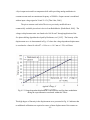
3.2.
Convergence of Ks and Kc for ψ = 6 rad, θ = 5 rad and d = 10%.
39
Fig.
3.3.
Convergence rate of Ks and Kc for ψ = 6 rad, θ = 5 rad and d =
10%.
40
Fig.
3.4.
Representation of Ks at 15% illumination duty cycle.
41
Fig.
3.5.
Representation of Kc at 15% illumination duty cycle.
41
Fig.
3.6.
Representation of Ks at 10% illumination duty cycle.
42
Fig.
3.7.
Representation of Kc at 10% illumination duty cycle.
42
Fig.
3.8.
Representation of Ks at 5% illumination duty cycle.
43
Fig.
3.9.
Representation of Kc at 5% illumination duty cycle.
43
Fig.
3.10.
Mask defined by the equivalency of Ks and Kc, d = 5%.
45
Fig.
3.11.
Mask defined by the equivalency of Ks and Kc, d = 15%.
45
Fig.
3.12.
Reference excitation amplitude and phase versus illumination
duty cycle.
46
-vi-
Fig.
Fig.
3.13.
4.1.
Phase constant magnitude versus illumination duty cycle. The
optimal operation range shown is within d = 14% to 18.5% and
limited to 50% of the maximum magnitude.
47
Schematic representation of PMI system described in this
Thesis.
49
Fig.
4.2.
Linnik configured interferometer [Wyant, 2002; Kreis, 2005].
50
Fig.
4.3.
PL-A741 quantum efficiency curve, peak λ = 660 nm
[PixeLINK, 2006].
51
OD-620L spectral output showing peak and full width at half
modulation points for determination of coherence length, lc. lc
is determined to be 16.8 nm [Opto Diode, 2006].
52
Voltage dependent displacement of the actuator used for phase
modulation during the experimentation conducted within this
Thesis.
53
Fig.
Fig.
4.4.
4.5.
Fig.
4.6.
Sample front panel of developed LabVIEW™ interface.
56
Fig.
4.7.
Sample of developed LabVIEW™ block diagram.
57
Fig.
5.1.
Recorded USAF 1951 negative glass target with group 7
outlined for containing the smallest resolvable element set
[Edmund Optics, Inc., 2006].
63
Spline-fit intensity profile of pixels extracted along horizontally
oriented bars in Group 7 of the USAF-1951 negative glass
target.
64
500Å ± 2.5% goal film NIST traceable gauge used for
characterization of optoelectronic holographic methodologies
[Veeco Metrology Group, 2002].
65
Interferograms acquired with phase modulating interferometry
(a); and with phase stepping interferometry (b).
67
Sine, cosine and arctangent maps calculated with phase
modulating interferometry (a); and with phase stepping
interferometry (b).
69
Deviations from planarity as determined by difference analysis
using phase modulating interferometry operating at f = 100 Hz,
d = 14% indicated a nominal film thickness of 503 Å ± 7 Å
under PMI. PSI methods indicated a nominal film thickness of
501 Å ± 7 Å [Furlong, 2007].
70
Fig.
Fig.
Fig.
Fig.
Fig.
5.2.
5.3.
5.4.
5.5.
5.6.
-vii-
Fig.
Fig.
Fig.
Fig.
Fig.
Fig.
5.7
5.8.
5.9.
5.10.
5.11.
5.12.
Shape of reference flat recovered with sinusoidal modulation
operating at f = 10 Hz and demonstrating a surface flatness of
λ/4.
75
Shape difference map, δ, between sinusoidal modulation and
phase stepping. Both measurements performed at the
operational frequency of f = 10 Hz. The sinusoidal variation,
having amplitude of 0.4 nm and frequency of 3.4 cycles/mm, is
attributed to a combination of the mean and mean squared
errors in both the PMI and PSI systems. These errors are
related to the phase modulation parameters and appear with a
spatial frequency equal to twice the optical frequency, as
explored in Appendix B and Creath [1988; 1992].
76
Wrapped phase map generated with sinusoidal modulating
interferometry imaging a reference flat at f = 100 Hz and d =
14% showing points used in calculation of optical phase drift.
80
Optical phase drift over time recovered with phase stepping
interferometry and sinusoidal phase modulating interferometry
operating at f = 2 Hz and f = 100 Hz respectively with d = 14%.
Under these operating conditions, the PSI method exhibits a
mean phase drift 7.5 times that demonstrated with PMI
correlating with results presented by Kinnstaetter, et al. [1988]
and Sasaki, et al. [1990b].
80
Scanning electron microscopy image of a prototype µHexFlex
device [courtesy of: Shih-Chi Chen, MIT, 2004].
82
Layered TMA structure of µHexFlex device viewed through a
scanning electron microscope [courtesy of: Shih-Chi Chen,
MIT, 2004].
83
Fig.
5.13.
Recovered shape of 280 µm diameter central stage µHexFlex.
85
Fig.
5.14.
Recovered shape of 375 µm diameter central stage µHexFlex
demonstrating damage to the armature structure.
86
Recovered shape of 540 µm diameter central stage µHexFlex
using phase modulating interferometry with damage indicated
to the TMA and armature structures.
87
Recovered shape of 540 µm diameter central stage µHexFlex
using phase stepping interferometry.
88
Relative displacement points on central stage and substrate
connection of active TMA.
90
Fig.
Fig.
Fig.
5.15.
5.16.
5.17.
-viii-
Fig.
Fig.
Fig.
Fig.
5.18.
C.1.
C.2.
C.3.
Displacement of the damaged µHexFlex device versus applied
voltage as determined through the system developed in this
Thesis.
91
Settings 1: Basic software controls, Base camera settings, Save
Results.
116
Settings 2: Image processing settings, Output voltage controls,
Save Results.
117
Settings 3: Operation/Plot mode, Camera triggering controls,
Save Results.
118
Fig.
D.1.
Block diagram of developed LabVIEW™ system.
120
Fig.
D.2.
Block diagram case structure set 1.
121
Fig.
D.3.
Block diagram case structure set 2.
122
Fig.
D.4.
Block diagram case structure set 3.
123
Fig.
D.5.
Block diagram case structure set 4.
124
Fig.
D.6.
Block diagram case structure set 5.
125
Fig.
D.7.
Default event, when there has been no changes on the user
interface, continue program with all prior settings.
126
Event structure 1a, when the gamma has been adjusted: Stop the
camera feed while adjusting the camera gamma value and
restart the camera feed.
127
Event structure 1b, when the gamma has been adjusted:
adjusting the camera gamma value when the camera is not
providing an image feed.
128
Event structure 2, if the shutter exposure time has been
adjusted, send the new value to the camera system. This setting
is not read when the camera is operating in “Low Integrate”
trigger mode.
129
Event structure 3a, update the current camera trigger settings
based on parameters found on the user interface and operate
under the new settings. Parameters are explained in Appendix
F.
130
Event structure 3b, update the current camera trigger settings
based on parameters found on the user interface. Deactivate
reading of the trigger settings for camera operation.
131
Event structure 4, this event enables the “Trigger Update”
button on the interface to set triggering parameters on selected
camera system.
132
Fig.
Fig.
Fig.
Fig.
Fig.
Fig.
D.8.
D.9.
D.10.
D.11.
D.12.
D.13.
-ix-
Fig.
Fig.
Fig.
Fig.
Fig.
Fig.
Fig.
Fig.
Fig.
Fig.
Fig.
D.14.
D.15.
D.16.
D.17.
D.18.
D.19.
D.20.
D.21.
D.22.
F.1.
F.2.
Event structure 5a, this event begins the display of the
unprocessed camera feed if the trigger signal is being generated
at a frequency above 0 Hz.
133
Event structure 5b, this event displays the unprocessed camera
feed but does not allow for image processing when ether the
camera trigger signal is not output or the modulation frequency
is set to 0 Hz.
134
Event structure 6, this event reads the current value of the
“Wrapped Phase Map” and “Modulation” buttons from the user
interface.
135
Event structure 7, this event sets the gain value of the acquired
images based on the currently selected value on the user
interface.
136
Event structure 8a, this event stops the current image feed to set
the pixel addressing mode and value as explained Appendix F.
It then re-starts the feed stream and re-opens any image displays
if previously enabled.
137
Event structure 8b, this event sets the pixel addressing mode
and value as explained Appendix F when the camera feed has
not been enabled.
138
Event structure 9a, Event Structure 9a, this event stops the
current camera feed to alter the region of interest (ROI) within
camera view both in size and location. ROI values must be
multiples of 8 and width/height must be equal for proper display
and processing. No error checking has been implemented to
ensure that the selected ROI is within the imaging array area.
139
Event Structure 9b, this event alters the region of interest (ROI)
within camera view both in size and location when camera feed
is not previously enabled. Restrictions from figure D.20 apply.
140
Event structure 10, this event calculates the modulation and
synchronization parameters for output voltage generation based
on current UI settings and data read from the excitation
parameter file (Default Excel file is excite.xls).
141
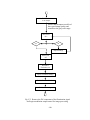
Turn on the developed code and ensure that the raw camera
feed is ready for processing.
148
Remove the DC component of the illumination signal and begin
modulation output control for image processing.
149
-x-
Fig.
F.3.
View the wrapped phase map or the optical modulation map
and save the results to the selected directory. End the program
using the implemented program stop.
-xi-
150
LIST OF TABLES
Table
2.1.
Microsensor families.
Table
2.2.
Comparison of phase evaluation methods without a spatial
carrier Sasaki, et al., 1986a; [Dorrio and Fernandez, 1998;
Dubois, 2001, Kreis, 2005].
24
Reference excitation amplitude and phase versus illumination
duty cycle.
46
Table
3.1.
8
Table
4.1.
System connectivity chart.
50
Table
5.1.
Shape measurement comparison between sinusoidal
modulation and phase stepping.
75
Mean optical phase map drift under phase stepping
interferometry at f = 2 Hz and sinusoidal modulating
interferometry at f = 10 Hz and 100 Hz.
81
89
Table
5.2.
Table
5.3.
µHexFlex quasi-static loading conditions.
Table
E.1.
Virtual instruments installed with LabVIEW™ IMAQ
modules.
143
Programming control blocks required for operation of the
PixeLINK PL-741 monochrome CMOS camera system.
144
Table
E.2.
-xii-
NOMENCLATURE
〈 〉
infinite time average
〈Δφ〉
mean optical phase map drift, mrad
〈X〉rms
geometric or root-mean-squared average of data set x
α
reference modulation phase, rad
Δλ
spectral output width at half output power
Δφ
Unwrapped recovered optical phase, rad
Δψactual
actual modulation step during phase stepping
Δψideal
ideal modulation step during phase stepping
Δt
Acquisition time, sec
ε
optical phase error, rad.
εXY
strain component in XY-plane
γ
fringe contrast
λ
wavelength of illumination source
λ0
primary diode output wavelength
η
tangent of the optical phase with additive noise contribution
ψ
mirror excitation phase, rad
σ
standard deviation of data set x
σXY
stress component in XY-plane
φ
interference phase distribution, rad
φR
reference phase modulation, rad
Σs, Σc
linear combinations of four sequential frames
θ
relative phase between illumination and reference modulation
ω
reference mirror excitation frequency, rad
angular frequency of illumination
d
illumination/camera exposure duty cycle
f0
f0
natural frequency of an unloaded piezoelectric actuator
′
i, j
natural frequency of a piezoelectric actuator with additional mass
orthogonal coordinates
-xiii-
k
wave number, 2π/λ
kz
wave vector, wave number taken in the z-direction
l
optical path length, reference arm
lc
coherence length of illumination source
ll
line length of the USAF 1951 target
m
power series index
meff
effective mass of a piezoelectric actuator equal to 1/3 the mass of
the ceramic stack
n
general Gaussian zero mean additive noise contribution
n′
total number of elements in data set x
n1, n2, n3, n4, np
additive noise on sequential frames, Gaussian zero mean noise
p
acquired frame number: 1,2,3, or 4
t
time, sec
tmin
minimum settling time of a piezoelectric actuator.
x
one to multi-dimensional data set
xij, xk
data point within data set x
(x,y)
spatial coordinates on the imaging array
z
amplitude of sinusoidal phase modulation, nm
CD
compact disk containing installation files included with this Thesis
CMOS
complementary metal oxide semiconductor
D
optical path length difference
|D|
mean absolute deviation
E
isotropic modulus of elasticity
E0
electrical field strength of a planar illumination wavefront
E1, E2, E3, E4, Ep
discreet complex amplitude of sequential frames, frame: 1, 2, …p
G
isotropic bulk modulus
I
intensity of an illumination source
I1, I2, I3, I4, Ip
continuous complex amplitude of sequential frames,
frame: 1, 2, 3 …p
IB
instantaneous photon flux or unmodulated dc component of an
illumination intensity
B
-xiv-
IB
average photon flux or unmodulated dc component of an
illumination intensity
IM
instantaneous modulated irradiance intensity
IM
average modulated irradiance intensity
IRQ
inter-quartile range
Jn(Y)
n-order Bessel function of the first kind, with respect to variable y
Ks, Kc
sine and cosine phase constants, respectively
LIGA
acronym for a German fabrication process involving Lithographie,
Galvanoformung, Abformung
M
additional mass coupled to a piezoelectric actuator
MEMS
microelectromechanical systems
N
N-bucket phase stepping algorithm
Ns, Nc
summed additive noise contribution
NDE
nondestructive evaluation
NIST
National Institute of Standards and Technology
OEHM
optoelectronic holographic methods
PMI
phase modulating interferometry
PSI
phase-shifting interferometry
QXY
stiffness matrix, XY component
R
Pearson product-moment correlation coefficient
ROI
region of interest within a full field of the imaging array
RMS
root-mean-square
T
reference modulation period, sec
TMA
thermomechanical actuator
UI
user interface
V
interference fringe contrast or the magnitude of the complex
quantity whose phase describes the position of the constructive
and destructive interference regions relative to a reference
X, Y
arbitrary constants
Z
recovered shape, nm
-xv-
OBJECTIVE
The objective of this Thesis is the review and implementation of a wavefront
sensing technology as an alternative to traditional phase stepping or phase-shifting
methodologies. It is expected that this will allow for a reliable measurement resolution of
1 nm, or better, allowing for nondestructive shape and displacement characterization of
MEMS devices. This Thesis will compare results obtained under multiple modulation
frequencies to those obtained with low frequency phase-shifting interferometry to
demonstrate the quality of the developed system under high modulation frequencies.
-1-
1. INTRODUCTION
Microelectromechanical systems (MEMS) have evolved from the integrated
circuit (IC) industry as an effort to radically miniaturize the scale of electromechanical
systems while increasing performance and decreasing the cost of the final product. These
goals evolved from the success of the IC industry with their bulk-fabrication techniques
and their incredible economies of scale [Judy, 2001]. Today, MEMS has come to
represent an entire field of systems in the nanometer to millimeter size, excepting IC
devices, where the smallest characteristic dimension is on the order of a micron [Judy,
2001; Hsu, 2002; Pryputniewicz, 2005; Kuppers, et al., 2006]. The scale of these devices
from ~10 nm to 1 mm is shown in Fig. 1.1 relative to other common microscale and
mesoscale systems.
Fig. 1.1. Scale of various microscopic systems with comparison
to MEMS [Zhang, 2004].
During the development of early MEMS devices, it became apparent that bulk,
continuum material property data could no longer be applied when working at scales
-2-
where crystalline structure and thermo-mechanical fabrication effects became dominant
factors. At the microscale, these effects create variations in material properties between
and within fabrication batches [Osterberg and Senturia, 1997; Rai-Choudhury, 2000].
Similarly, miniaturization required a new approach to system design due to the effects of
force scaling. To ensure that MEMS devices function as designed, many are enabled
with integrated microstructures for in-situ measurements of material properties [Liwei, et
al., 1997; Osterberg and Senturia, 1997; Sandia, 2006]. However, these microstructures
require additional space on the fabrication wafers that could be spent providing additional
mechanical complexity or allowing for an increase in the number of devices and hence an
improvement in the economics of fabrication and design. Consequently, noninvasive,
noncontact techniques are needed to measure the geometric and material property data
over the full device.
For materials characterization, scaling laws require a measurement resolution of
0.1 – 1 nm in MEMS structures. Interferometric techniques are needed to achieve this
accuracy over a full field of view. The invention of phase-shifting interferometry (PSI)
was a major breakthrough in the field of homodyne interferometry, providing a method to
measure the optical phase with unprecedented accuracy [Creath, 1992]. Implemented on
almost all types of interferometric imaging systems, through use of various algorithms,
PSI allows extraction of a phase map from several intensity fringe patterns. Classic
phase-shifting interferometry requires integration of 3 or more intensity maps during a
linear variation in the optical phase over a 2π phase variation [Creath, 1988; Kreis, 2005].
Later, phase stepping interferometry was developed where the intensity integration
occurs at discreet phase steps. These techniques provide an RMS accuracy of λ/100 in a
-3-
well-calibrated system [Creath, 1988]. As the acquisition speed increases, the phase error
level increases due to increasing phase-shift miscalibration error. At high frequency, the
reference excitation waveform becomes distorted due to jerk and other inertial effects on
the reference mirror. Increasing the number of recorded interferograms reduces the
degradation in the recovered phase-shift error at the expense of increasing processing
time [de Groot, 1995a].
This Thesis implements phase modulating interferometry (PMI) as an alternative
technique to minimize the impact of rapid acquisition speeds on the recovered phase map
while providing measurement resolution on the order of 1 nm or better. When initially
proposed by Sasaki and Okazaki [1986a], phase modulating interferometry combined 4
bucket integration with a sinusoidal reference excitation providing continuous reference
motion with a waveform that will remain undistorted at high excitation frequencies. A
variant of this initial work has been developed that operated in quadrature under
stroboscopic illumination. These variations allow for both the rapid acquisition of
interferograms and the use of stop-illumination techniques for the capture of rapid
motions, vital in dynamic and in-situ measurements of MEMS devices.
Unlike commonly used PSI methods, PMI requires reference excitation amplitude
of less than the illumination wavelength. However, this excitation amplitude is a strongly
non-linear function of the stroboscopic illumination duty cycle. Additionally, both the
quadrature and integrating bucket methods require a known phase difference between the
illumination/acquisition period and the reference excitation period [Dubois, 2001; Sasaki,
and Okazaki, 1986a]. Additive noise concerns of the PMI system are presented in this
Thesis and used in the determination of the reference excitation amplitude and phase.
-4-
Error in the recovered phase map is then proportional to the error in these two
parameters.
The phase modulating system, reported in this Thesis, was implemented in a
Linnik configuration and is controlled with software designed in the LabVIEW™
graphical programming environment [LabVIEW™ 7.1, 2006]. The implementation
required synchronization of the illumination source with the reference excitation and
camera acquisition time. Representative Results are presented showing feasibility of the
developed PMI technique for high resolution measurements of shape and semi-static
loading situations of MEMS.
-5-
2. BACKGROUND
MEMS, or microelectromechanical systems, is an approach to fabrication that
uses the materials and processes of microelectronics fabrication to convey the advantages
of miniaturization, multiple components and microelectronics to the design and
construction of integrated microstructures and electromechanical systems [Hsu, 2002;
MEMS Industry Group, 2006]. In development since the late 1960s, MEMS has evolved
from the integrated circuit industry as an effort to radically miniaturize operation scale
over traditional mesoscale devices while increasing performance and reducing product
cost [Judy, 2001]. As an enabling technology, MEMS revolutionized many industries by
allowing development of smart products, augmenting the computational ability of
microelectronics with the perception and control capabilities of microsensors and
microactuators and expanding the space of possible designs and applications [MEMS
Exchange, 2006].
According to MEMS Industry Group, MEMS and MEMS related applications
have rapidly grown 15% to 20% per year over the last decade into an estimated $8.3
billion dollar industry in 2007, as shown in Fig. 2.1, with one-third of that revenue in
pressure and inertial sensors, as presented in Fig. 2.2 [MEMS Industry Group, 2006].
-6-
USD (billions)
Fig. 2.1. Worldwide revenue forecast for MEMS [MEMS Industry Group, 2006].
Fig. 2.2. Share of MEMS revenues by device, 2007 [MEMS Industry Group, 2006].
From Figs 2.1 and 2.2, it is apparent that MEMS devices are found ubiquitously
throughout the modern world. Applications stemming from the groups presented in Fig.
2.2 include inertial navigation systems, integrated optomechanical components for image
display, embedded sensors and actuators for condition maintenance, shown in Table 2.1,
and much more [Furlong, 2004a].
-7-
Position
Table 2.1. Microsensor families.
Pressure
Inertial
Magnetometers
Thermal
Chemical
Radio frequency
Electrochemical
Field effect transistors
Biosensors
Molecular-specific
Cell-based
Neural systems
Gas
Fluid Flow
Much of this industry growth is focused on the development of micro-sensors
with higher spatial resolutions and temporal bandwidth than their macroscale
counterparts while requiring less operating power [Judy, 2001]. Typically, it can take 10+
yrs and millions of dollars to develop a new sensor or a MEMS platform.
Over the years, most of the development money has been spent on pressure
sensors and accelerometers and, as such, these two areas are the furthest developed
MEMS technology [Electronic Design, 2000; MEMS Industry Group, 2006]. However,
little standardization exists within industry in all but the simplest designs though
organizations, such as the American Society of Mechanical Engineers and the Institute of
Electrical and Electronics Engineers, have begun developing standards for adoption as
industry norms. With increasing commercialization, there has been a greater push
towards the acceptance of these standards particularly in MEMS testing and packaging
procedures.
Testing issues must be included in the overall design of the device/package in the
early phase of development to minimize the final cost of the device. Modern testing can
be as much as 33% of the overall development cost of a MEMS device [MEMS
-8-
Exchange, 2006]. Testing can and must occur at multiple stages of MEMS development
as illustrated in Fig. 2.3. This figure presents a typical MEMS development cycle with
testing requirements at each stage of the design process. These tests include materials
characterization during fabrication and accelerated lifecycle testing to ensure the
longevity of the developed components.
Fig. 2.3. MEMS development cycle [Exponent, Inc., 2000].
A major concern within these testing procedures is the unknown reliability of
many MEMS devices due to uncertainty in the long-term stability of these devices. As a
consequence of scaling in micro-components and fabrication variability, bulk, continuum
material property data are not applicable to MEMS devices where crystalline structure
and thermo-mechanical fabrication effects are dominant factors. Only greater knowledge
of the basic material properties and failure mechanisms of the materials employed in
-9-
MEMS designs will allow for a wider acceptance of these systems [MEMS Industry
Group, 2006].
2.1. MEMS material property variation
MEMS fabrication falls into three main families: surface micromachining, bulk
micromachining, and lithographic techniques [Hsu, 2002]. Surface micromachining is
based on the deposition and etching of different structural layers. Starting with a silicon
wafer or other substrate, layers are grown and selectively etched by a wet or dry etch
involving an acid or ionized gas respectively. While surface micromachined components
may someday grow to as many layers as is needed, modern MEMS devices use up to five
structural layers [Pryputniewicz, 2005; Sandia, 2006].
Bulk micromachining defines structures by selectively etching inside a substrate
creating structures within a substrate. Like surface micromachining, bulk
micromachining can be performed with wet or dry etches. As this process involves the
selective removal of material, the particular etchant used is strongly dependant on the
fabrication speed and quality requirements. Wet isotropic etching provides the same etch
rate in all directions while undercutting masking material. Wet anisotropic etch rate
depends on the crystalline plane orientation within the substrate material. Consequently,
the lateral etch rate can be much larger or smaller than the vertical etch rate and resulting
structures have angled walls, with the angle being a function of the crystal orientation of
the substrate. Dry etching involves the removal of material by gaseous etchants though
requires the periodic deposition of an etching protective material to minimize the side
-10-
wall angle in an etched cavity [Rai-Choudhury, 2000; Hsu, 2002; Krauss, 2002; Furlong,
2004a].
Lithographic techniques include the LIGA molding process. LIGA, a German
process, is an acronym for X-ray lithography (Lithographie), electroplating
(Galvanoformung), and molding (Abformung). Developed in the 1980s, LIGA was one
of the first major techniques to allow for manufacturing of high-aspect-ratio structures
with lateral dimensions below one micron and thicknesses up to 500µm [Hsu, 2002;
Furlong, 2004a]. This technique allows for the creation of 3-D microstructures defined
by 2-D lithographic patterns. The height-to-width ratio capability is relevant to the
manufacturing of miniature components that can withstand high pressure and
temperature, and can transfer useful forces or torques [Sandia, 2006].
Variation in the structure and material properties of MEMS devices exists
between fabrication sites and within fabrication batches. Consequently, the material
properties of a common MEMS material deposited by one manufacturer can vary
substantially from that deposited by another. Further variation is present between and
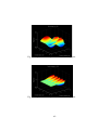
within wafer batches during production runs [Exponent Inc., 2000]. As seen in Fig. 2.4, a
silicon nitride film applied across a single crystal silicon wafer may exhibit a nonlinear
spatial variation in residual stresses on the order of 20 MPa. This variation illustrates the
need for full field of view testing for accurate characterization of the fabricated
structures.
-11-
Fig. 2.4. Variation in residual stress and biaxial modulus
across a silicon wafer [Exponent, Inc., 2000].
Much of this material property and fabrication property variation is due to the
particular application of many materials used in MEMS structures. Silicon and other
materials had been commonly used in the integrated circuit industry for decades.
However, their application as thin film structures results in numerous mechanical
properties which must be known for each material where traditionally only electrical
characterization was required [Judy, 2001]. As with meso- and macroscale structures,
critical mechanical properties include elastic modules, yield strength, fracture toughness,
fatigue resistance, corrosion resistance, creep behavior, and residual stress.
Similarly, the novel capabilities of MEMS devices allow for operation under
conditions unknown in the macro world. Micromirrors found on the DigitalMicromirror
Device from Texas Instruments, Inc. commonly operate in excess of 1 trillion of cycles
without failure [Douglass, 1998]. However, this total number of accumulated actuation
cycles extends far beyond what has been required in "macro" applications. As with
-12-
macroscale devices, microscale devices can experience fatigue and wear from contacting
surfaces during individual actuation cycles. However, little information about fatigue or
wear is available under these conditions for either macro- or MEMS devices. As a result,
lifetime predictions are device specific and, due to fabrication variations, are not always
largely validated by statistics [Rai-Choudhury, 2000].
2.2. Nondestructive evaluation of MEMS
Nondestructive evaluation (NDE) is used to “evaluate prototype designs during
product development, to provide feedback for process control during manufacturing, and
to inspect the final product prior to service” without affecting the object’s future
usefulness [Shull, 2002]. The basic principle of NDE is finding and measuring physical
phenomena that will interact with and be influenced by the test specimen without altering
functionality. Functionally, choosing the proper NDE method from all available
techniques requires considering of the following factors:
1) understanding the physical property to be inspected.
2) understanding the physical properties of the NDE methods.
3) understanding the interaction between the method and the test sample.
4) understanding the potential and limitations of the technology.
5) understanding of surrounding economic, environmental, and other factors.
-13-
Before using any NDE method, there must be some knowledge of the properties
of interest. In MEMS, an investigator may be interested in the modulus of elasticity of an
object of interest. This requires information on how modulus of elasticity may be
calculated or how it may affect the system of interest, whether through dynamic or static
effects. This knowledge works to drive NDE method choice. If the structure of interest
is a laminated plate with homogenous and isotropic material properties, modulus of
elasticity may be determined through investigation of the stress-strain relationships
within that structure, assuming an application of general plate theory, the Kirchhoff
hypothesis, and planar stress. These assumptions allow for calculation of the modulus of
elasticity, bulk modulus, and Poisson’s ratio within that object, assuming knowledge of
the applied stresses and resultant strains [Boresi and Sidebottom, 1985; Guckel, et al.,
1985]. Many NDE methods may be used to extract the stress and/or strain information
needed for these calculations.
Larger samples may use an ultrasonic technique for determination of these elastic
constants by investigating wave propagation through the sample, though typically this
requires contact by a transducer/receiver. In a small system, this contact may have a
significant influence on the recovered data. An X-ray system may be used in 2-D or 3-D
as a way to measure the shape and hence deformations of the object of interest. The
major disadvantages to this technique are the high cost, danger, and potential for imaging
artifacts to make analysis difficult. Positively, X-ray computed tomography has been
applied to objects from 5 µm to 2 m which is on the scale of MEMS devices [Haddad, et
al., 1994; Tonner and Stanley, 2002]. Similarly, various optical techniques exist which
allow for shape measurements of the system of interest. As with X-ray computed
-14-
tomography, this shape information is then used to determine the deformations of the
system of interest and hence the strains resulting from an applied stress. However, unlike
X-ray methods, optical techniques have demonstrated subnanometer shape measurement
resolution.
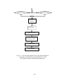
2.3. Interferometric options
Interferometry uses changes in an optical wavefront to measure how an object
behaves under loading. Where many techniques exist to record these changes, each have
different strengths and weaknesses when used in a NDE application. Modern techniques
include, and are not limited to, the following categories: homodyne interferometry,
spatial and temporal heterodyne interferometry, digital holographic interferometry, and
white light interferometry [Dyson, 1970; Sirohi and Kothiyal, 1991; Greivenkamp and
Bruning, 1992; Wyant, 2002; Kreis, 2005]. Homodyne systems consider the relative
optical phase-shift between coherent reference and object beams. In a multiple path
interferometer, the relative phase between the two beams is directly proportional to the
wave number, k, and the shape of the object of interest, Z. A Michelson-type
interferometer, presented in Fig. 2.5., recovers shape proportional to twice the optical
path length difference, D.
-15-
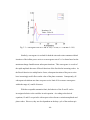
Point detector
Light source
Beam
splitter
Reference
mirror
l
l
D
Object
Fig. 2.5. Michelson interferometer [Kreis, 2005].
The object shape can then be recovered as
Z=
Δφ
Δφ Δφ ⋅ λ
=
=
,
2 ⋅ k 4π
4π
(2.1)
λ
where λ is the illumination wavelength, Δφ is the recovered optical phase, and k is the
wave number along the optical path [Kreis, 2005]. Typical methods for extraction of the
optical phase from acquired interferograms include phase stepping or phase-shifting of
the reference beam path length. The optical phase map magnitude and directionality can
then be solved for by acquisition of three or more interferograms with relative phase
differences [Kreis, 2005].
Phase stepping interferometry can be separated into temporal and spatial methods.
In this Thesis, all comparisons are made with regards to temporal phase-shifting which
requires that the phase be stepped with time, usually in a uniform manner within the
whole field by using a modulator device [Creath, 1988; Greivenkamp and Bruning,
1992]. During this process, a series of interferograms with a certain phase increment
between them is obtained. Once these phase-shifted patterns have been combined using a
-16-
phase-shifting algorithm, we can obtain the phase values modulo 2π for all of the full
field of view points simultaneously. This method can provide as accuracy level of up to
λ/1000 if the ambient conditions and experimental setup are well controlled [Creath,
1988, 1992; Haasteren and Frankena, 1994; Dorrio and Fernandez, 1998]. However, due
to the need to obtain different separate patterns in time, temporal phase stepping methods
cannot be applied to dynamic processes without the application of a stroboscopic
illumination source or implementation of an acquisition system that is rapid relative to
the dynamic processes being studied as standard methods assume that the background
intensity, contrast, and phase be stationary over the interferogram acquisition period
[Creath, 1988; Kreis, 2005]. The number of interferograms acquired depends on the
particular phase extraction algorithm employed where larger numbers are used to reduce
sensitivity to systematic noise and environmental effects [Surrel, 1993; de Groot and
Deck, 1996; Ruiz, et al., 2001].
Historically, temporal phase-shifting algorithms were restricted to combinations
of three or four interferograms where modern algorithms have been demonstrated with
linear combinations of up to seven interferograms [Hariharan, et al., 1987; de Groot,
1995a; Surrel, 1996]. Using windowing to increase the insensitivity to variations in
phase steps has become a common practice with the acquisition of seven or more
interferograms as the larger the data set, the more accurately it can be windowed [de
Groot, 1995a; Schmit and Creath, 1996; Ruiz, et al., 2001].
In terms of performance, the four bucket PSI algorithm has been shown to be a
significant improvement over the three-bucket algorithm with regards to vibration
sensitivity, at the cost of slightly larger memory requirements and slightly longer
-17-
processing time [Surrel, 1993; de Groot, 1995a; Ruiz, et al., 2001]. A five bucket
algorithm analyzed by Hariharan, et al. [1987] has been shown to be minimally sensitive
to small phase step errors at the expense of increased processing time and memory
requirements. While increases in the number of acquired data samples correlates with a
decrease in sensitivity to phase step errors, the number of data samples is typically
limited by processing speed, computer memory limitations, and “the limited phase-shift
range of piezoelectric transducer actuators” [Surrel, 1993; Deck, 2003].
Spatial phase-shifting interferometry differs from temporal phase-shifting
interferometry by simultaneously acquiring a set of phase-shifted interferograms while
preserving the measurement accuracies of temporal phase-shifting. These interferograms
are either captured on multiple imaging devices or on a singular array that is later
subdivided numerically [Koliopoulos, 1992; Dorrio and Fernandez, 1998; 4D
Technology, Inc., 2006]. A spatial separation of the interferograms can be achieved with
rotational polarizing components, diffraction gratings, or computer generated diffractive
optical elements [Dorrio and Fernandez, 1998; North-Morris, et al., 2002; 4D
Technology, Inc., 2006]. In this method, errors due to environmental instabilities are
avoided with the simultaneous acquisition of the patterns. However, other types of errors
appear due to variations in the different camera systems used or within different parts of
the same imaging array [Koliopoulos, 1992]. Consequently, additional data processing is
needed to match the measurement accuracy of temporal phase stepping therefore realtime evaluation methods are obtained at the cost of measurement accuracy [Kwon, et al,
1987].
-18-
By contrast, temporal heterodyning uses the interference of two optical waves of
different frequencies which produces an intensity oscillating at a beat frequency equal to
the frequency difference [Sirohi and Kothiyal, 1991]. These systems split the reference
and object beams by use of an acousto-optic modulator. A Zeman splitter may be used to
separate the beam within the laser head, through use of powerful magnets [Chapman,
2002]. Another technique involves the use of a dual mode laser with beat frequency of 1
GHz or above. Alternatively, acousto-optic modulators can be used to shift the beam
path between multiple output angles creating a misalignment between the object and
reference beams. However, this approach increases the level of physical complexity
within the interferometric system while introducing a secondary frequency shift into the
reference beam requiring an additional photo-detector to determine the shifted beat signal
after modulation. Regardless of how the beat frequency is created, these systems
measure the returned optical phase by timing the arrival of zero crossings on the
sinusoidal illumination signal [Chapman, 2002].
Spatial heterodyning relies on the addition of a carrier frequency on the
interference pattern. This technique, alternatively known as a Fourier-transform method,
was proposed as an alternative to traditional homodyne and heterodyne techniques
[Takeda, et al., 1982]. A spatial carrier frequency may be generated interferometrically
though the addition of a tilt to the reference mirror in a homodyne system or through the
use of a holographic grating. Modern applications include projection of a computer
generated fringe pattern allowing for the determination of optical phase through a single
interferogram while solving for the sign ambiguity problem. This technique relies on the
projection or creation of a carrier fringe pattern higher than the spatial variations present
-19-
within the recovered optical phase. This condition limits the measurement resolution of a
spatial heterodyne system to the ability of the holographic system to both project and
recover the carrier frequency signal without aliasing [Kreis, 2005]. However,
measurement accuracy of both spatial and temporal heterodyne interferometry has been
found to be on the same order as temporal phase stepping interferometry though typically
requiring greater experimental complexity and processing time [Dorrio and Fernandez,
1998].
Digital holography uses a digital imaging system to record holograms for later
numerical reconstruction [Kreis, 2005]. The angle between the object and reference
wavefronts must be controlled to produce holograms which are resolvable by a given
imaging system. Recovery of the object surface requires the numerical reconstruction of
the wavefront at the image plane by use of the Fresnel transform [Kreis, 2005]. The
image plane or observation plane appears at the coordinates where the real image can be
reconstructed. At this plane, the wavefront reflected from the object of interest converges
to a sharp image. Shape information can then be extracted from the calculated object
wave field. Phase-shifting digital holography, involving the capture of three or more
digital holograms with a mutual shift in the reference wave, can be used for shape
characterization of MEMS [Furlong and Pryputniewicz, 2003]. The primary advantage
to the phase-shifting approach is the elimination of the DC-component and twin image
within the reconstructed wave field though at the expense of an increased system stability
requirement [Kreis, 2005]. If these stability requirements are met, digital holographic
methods have been shown to be λ/100 accurate [Dorrio and Fernandez, 1998; Mann, et.
al, 2005].
-20-
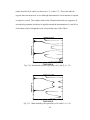
White-light interferometric techniques rely on the application of a short coherence
length white light source instead of the more commonly used laser light sources as
demonstrated in Fig. 2.6 [Wyant, 2002; Kreis, 2005]. Traditionally, laser light has been
used as its long coherence length simplifies the procedures required for the creation of
interference fringes as the interferometer path lengths no longer have to be matched as
closely as if a short coherence length white light source is used. However, laser light
interference fringes can appear within any stray reflections, possibly resulting in incorrect
measurements. The strict optical path length matching requirements of short coherence
white light systems eliminates this concern while providing a powerful measurement tool
[Wyant, 2002]. While homodyne phase-shifting interferometry has proven extremely
powerful and useful in many research and commercial systems, possessing a
measurement resolution of λ/100, the height difference between two adjacent data points
must be less than λ/4, where λ is the wavelength of the light source [Creath, 1988; Wyant,
2002]. If the slope is greater than λ/4 per detector pixel then height ambiguities of
multiples of half-wavelengths exist. However, the use of white light makes it possible to
connect fringe orders across this step at similar measurement resolutions.
Fig. 2.6. Monochromatic, red light, versus white light interferograms of a sample with
>λ/4 step discontinuities demonstrating the ability to connect fringe orders using white
light interferometry [Wyant, 2002].
-21-
Coherence probe interferometers are used to obtain height measurements on
structures exhibiting large steps or rough surfaces. With a short coherence length source,
good contrast fringes will appear only when the two interferometric paths are closely
matched. Consequently, if the path length of either the object or reference arms is
adjusted, the maximum fringe contrast will translate along the instrument sensitivity
vector. The height variations across the sample can then be determined by looking at the
locations at which the fringe contrast is maximized. As the translation of the fringe
contrast is controlled there are no sign ambiguities in the recovered height map.
Additionally, as the maximum fringe contrast is obtained when the sample is in focus,
there will be no focus errors during surface measurement [Caber, 1993; Wyant, 2002].
The major drawback of measurements with this type of scanning interferometer is
that only a single surface height is being measured at a time. As a result, transient event
may be overlooked or misinterpreted. Additionally, a large number of measurements and
calculations are required to accurately determine surface height values, where typical
sampling intervals can range from 50 to 100 nm. [Caber, 1993; de Groot, et al., 2002].
“To obtain the location of the peak fringe contrast, and hence the surface height
information, this irradiance signal is detected using an [imaging] array. The signal is
sampled at fixed intervals […] as the sample path is varied. [The signal is then digitally
filtered and rectified by square-law detection.] The peak of the filter output is located
and the vertical position corresponding to the peak is noted. Interpolation between
sample points can be used to increase the resolution of the instrument beyond the
sampling interval. This type of measurement system produces fast, non-contact, true
three-dimensional area measurements for both large steps and rough surfaces to
-22-
nanometer precision. [Wyant, 2002].” With this processing 0.1 nm accuracy levels have
been demonstrated [Zygo Corporation, 2006].
2.4. Benefits of phase modulating interferometry
While the invention of phase-shifting interferometry (PSI) was a major
breakthrough in the field of interferometry by providing a method to measure the optical
phase to an unprecedented accuracy, this Thesis proposes phase modulating
interferometry (PMI) for the nondestructive evaluation of MEMS devices [Creath, 1988;
Schwider, 1990]. Originally proposed in Sasaki and Okazaki [1986a, 1986b] and
expanded in Dubois [2001], this method answers some of the limitations inherent in
classic homodyne and heterodyne techniques while combining strengths of each. By
continuously modulating an illumination wave front and using a four bucket algorithm,
shown in Fig. 2.8, it has been demonstrated that a time-varying interference pattern can
be detected and analyzed to a measurement accuracy of 1.0 nm under a 600 nm
illumination source. This is possible because the amplitude and phase of the modulation
signal is chosen to minimize the effects of Gaussian additive noise on the recovered
optical phase map. As shown in Table 2.2 and discussed in Sasaki and Okazaki [1986a],
Sasaki, et al. [1990a, 1990b], Dubois [2001], and Dorrio and Fernandez [1998],
sinusoidal phase modulating interferometry has demonstrated an accuracy level of 0.1 nm
which is on par with that obtained with temporal phase modulating interferometry though
at the cost of higher processing complexity. This increased complexity is offset by an
increased immunity to static and dynamic environmental and systematic noise effects
-23-
below the modulation frequency versus both temporal and spatial phase stepping
interferometry [Sasaki and Okazaki, 1986a, 1986b; Creath, 1988; Suzuki, et al., 1994; de
Groot and Deck, 1996; Dorrio and Fernandez, 1998; Dubois, 2001; Kreis, 2005].
Table 2.2. Comparison of phase evaluation methods without a spatial carrier
[Sasaki and Okazaki, 1986a; Suzuki, et al., 1994; Dorrio and Fernandez, 1998;
Dubois, 2001, Kreis, 2005].
Method
Temporal
Spatial
Heterodyne
Sinusoidal
phase stepping phase stepping interferometric phase modulating
methods
methods
interferometry
methods
Required
continuous
≥3
≥3
≥4
interferograms
detection
Accuracy
very high
high
very high
very high
Influence of
static noise
Influence of
dynamic noise
Experimental
requisites
low
high
low
low
high
low
high
low
high
low
very high
very high
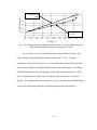
In Sasaki and Okazaki [1986a, 1986b] and Dubois [2001], the developed
interferometric systems operate under sinusoidal modulation in four integrating bucket
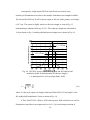
mode, as shown in Fig. 2.7.
-24-
I(t)
I1
0
I2
I3
I4
T/4 T/2 3T/4 T
Fig. 2.7. Simulation of the interferometric signal I(t) and how it
is integrated over the four quarters of the modulation period [Dubois, 2001].
According to Fig. 2.7, this integration is performed by a two-dimensional detector array
with a charge storage period equal to one-quarter of the period of the sinusoidal phase
modulation, T/4. Interferograms are then acquired over sequential quarters to generate a
set of four interferograms for data processing. This combination of sequential acquisition
periods each over one part of the modulation cycle is known as an integrating bucket
method. Sinusoidal modulation was chosen to minimize errors within the recovered
optical phase map by minimizing the jerk experienced by translation of a reference
mirror. PSI techniques involve 3 or more stepped motions of a reference mirror to solve
the underlying interferometric equations. Each stepped motion involves the rapid
acceleration and deceleration of the attached reference mirror. Increasing acquisition
speed results in greater operational jerk creating nonlinearities in the reference
modulation. A 10% modulation miscalibration error correlates with an error in the
recovered optical phase map of 0.20 radians in a 4-frame algorithm or ~20nm under a
620nm illumination source [Creath, 1992; Surrel, 1993]. An increase in the number of
acquired interferograms will reduce the phase error to 0.0796 radians at the expense of
-25-
increased processing requirements [Surrel, 1993]. The sinusoidal modulation of the PMI
system minimizes the jerk of the reference arm demonstrating a theoretical phase
measurement accuracy of less than 0.5 - 0.8 nm under a 600 nm illumination source
[Sasaki and Okazaki, 1986b]. Experimentally, these errors have been found to be from
0.5 – 1.0 nm when operating under a 200 Hz modulation signal [Sasaki and Okazaki,
1986a, 1990a; Dubois, 1999, 2001].
While the previously presented four-bucket method has been proven for the
analysis of static structures, the currently defined system has not been demonstrated with
dynamic studies. Due to the relatively long acquisition period, the observable intensity
field becomes modulated by the square of the zero order Bessel functions of the first
kind, J0(Y). In harmonic vibration studies, the fringes become contours of equal vibration
amplitudes at the spatial vibration nodes. Additionally, fringe contrast decreases with
increasing fringe order with the maximal contrast existing at the nodes of the vibration
mode [Kreis, 2005]. Application of a stroboscopic illumination signal converts the J0
fringes into a sinusoidally modulated fringe pattern, greatly simplifying extraction of the
optical phase map due to the complexity of the Bessel function term.
The focus of this work is the derivation and implementation of the phase
modulating interferometric system that uses both stroboscopic illumination and a reduced
exposure period. The addition of these physical attributes will allow for use of the PMI
system in both dynamic and static studies.
-26-
3. THEORETICAL ANALYSIS OF PHASE MODULATING
INTERFEROMETRY
Sasaki and Okazaki [1986a] and Dubois [2001] have presented the derivation of a
phase modulating system using the 4 integrating bucket method and a sinusoidal
reference excitation. This approach assumes a constant illumination source and requires
multiple excitation periods to fully capture the modulation waveform. The latter
limitation is based on the recording media used due to the finite time required between
interferogram acquisition periods. This prevents the continuous capture of a single
reference excitation waveform, particularly at the rapid reference excitation frequencies
required for rapid display of the wrapped phase map.
Additionally, this approach is limited with regards to dynamic systems as it
requires an exposure time which may be long compared to the period of excitation. This
situation is known as time average holographic interferometry. In this case, the intensity
of the recovered fringes is modulated by the zero order Bessel function of the first kind.
Stroboscopic illumination allows for an acquisition time which is on the order of
the dynamic system motion. As the illumination period becomes short relative to the
motion of the system of interest, the recovered interferogram is the same as that
recovered with double-exposure holographic interferometry and so is only modulated by
a cosinusoidal term. This results in the ideal case for optical phase recovery [Kreis,
2005].
To allow for the capture of both dynamic and static systems, the effect of
stroboscopic illumination on phase modulating interferometry is presented with a focus
on a sinusoidal reference excitation.
-27-
3.1. General derivation of phase modulating interferometry
with stroboscopic illumination
The intensity distribution of a holographic interferogram as recovered by an
imaging system is a function of the unmodulated DC component of an illumination
intensity, IB(x,y), the interference fringe contrast, V(x,y), and the interference phase
B
distribution, φ(x,y). At one instant of time, the full-field intensity is of the form
I (x, y ) = I B ( x, y ) ⋅ {1 + V ( x, y ) ⋅ cos[φ ( x, y )]} ,
(3.1)
I (x, y ) = I B ( x, y ) + I M ( x, y ) ⋅ cos[φ ( x, y )] ,
(3.2)
or
where IM(x,y) describes the modulated amplitude of interference fringes [Kreis, 2005].
Extraction of the phase distribution requires the solution of a system of equations due to
the multiple unknowns in the general equation. This system must also be posed in a way
that eliminates the phase ambiguity present in the above equations with respect to the
phase distribution due to the even, periodic nature of the cosine function. Traditional
phase-shifting and phase stepping methods provide a means for extraction of the optical
phase and solution of the sign ambiguity. This is accomplished through the acquisition of
multiple intensity distributions with mutual phase-shifts. Nonlinear equations, of the
form shown in Eq. 3.3, can then be solved for the optical phase over the full field of view.
When the reference phase-shift, φR(x,y), between each interferogram, is known a
minimum of three intensity distributions must be found to solve for IB(x,y), IM(x,y), and
B
φ(x,y) [Kreis, 2005],
I ( x, y ) = I B ( x, y ) + I M ( x, y ) ⋅ cos[φ ( x, y ) + φ R ( x, y )] .
-28-
(3.3)
While phase stepping or shifting rely, respectively, on discreet step or saw tooth
variation in the optical phase to provide the known phase term within recovered
interferograms, phase modulating interferometry uses a known continuously varying
phase variation [Sasaki and Okazaki, 1986a; Kreis, 2005]. In this Thesis, the
continuously variant signal is accomplished with motions of a piezoelectric actuator
attached to the reference mirror. Phase modulation is differentiated from phase-shifting
by eliminating the linear phase variation requirement, allowing for the application of a
continuous phase modulation function. With this implementation, the overshoot and
settling experienced by piezoelectric actuators during discontinuous motion can be
reduced or eliminated.
As shown in documentation from Physik Instrumente, L.P. [2005], piezoelectric
actuators undergoing discontinuous motions experience an instantaneous displacement
overshoot of 10 -15 % under low displacement steps. The actuator then requires a finite
settling time to attain its nominal displacement. As shown in Eq. 3.4, the minimum
settling time is related to the natural frequency of the actuator and attached components.
When operating below 10% of the resonant frequency, the minimum settling time is
given by [Physik Instrumente, L.P., 2005]
t min =
1
3 f 0'
.
(3.4)
The additional mass of the reference mirror and surrounding structure alters the natural
frequency of the unloaded actuator, f0. While the resonant frequency of the unloaded
actuator is normally given by a manufacturer, the loaded natural frequency, f0′, can be
found by
-29-
f 0' = f 0
meff
M + meff
,
(3.5)
where M is the additional mass coupled to the piezoelectric actuator and meff is the
effective mass of a piezoelectric actuator equal to 1/3 the mass of the ceramic stack
[Physik Instrumente, L.P., 2005]. For a piezoelectric actuator with a resonant frequency
of 2 kHz and negligible loaded masses, the minimum settling time will be approximately
0.5 ms. This settling time will be greatly increased at modulation frequencies
approaching the effective natural frequency and with the attachment of masses to the
piezoelectric stack.
The significant overshoot coupled with the settling time may result in an average
modulation error of 5 - 10% during phase stepping [Surrel, 1993]. As phase stepping
relies on constant phase steps, this modulation error will correspond to a mean error in
the recovered optical phase map described by Eq. 3.6 [Surrel, 1993],
ε =
1
⎛ 2π
2 N sin ⎜
⎝ N
Δψ actual
⋅ 2π .
⎞ Δψ ideal
⎟
⎠
(3.6)
From Eq. 3.6, it is apparent that the mean optical phase map error decreases with larger
N-bucket algorithms and increases with larger modulation errors. For the case of a 5%
modulation error, the mean phase error becomes 39.25 mrad for N = 4.
As shown, this modulation error may be due to actuator overshoot and settling
time, however, other factors including hysteresis and creep may contribute to an error in
the modulation step [Physik Instrumente, L.P., 2005]. Hysteresis and creep describe
positional errors during open-loop operation due to crystalline polarization effects and
molecular effects within a piezoelectric material. “The amount of hysteresis increases
-30-
with increasing voltage applied to the actuator. The “gap” in the voltage/displacement
curve of a piezoelectric actuator typically begins around 2% and widens to a maximum of
10% to 15% under large-signal conditions. If, for example, the drive voltage of a 50 µm
piezoactuator is changed by 10%, the position repeatability is on the order of 1% of full
travel or 1 µm [Physik Instrumente, L.P., 2005].” Creep is a change in displacement with
time without corresponding changes in the voltage source due to changes in the remnant
polarization changes within the piezoelectric material. For rapid to moderate acquisition
systems, the effect of creep on the resulting phase map errors will be minimal as, in
practice, creep is typically a few percent over an hour [Physik Instrumente, L.P., 2005].
Phase modulating interferometry minimizes both hysteresis and creep effects relative to
phase stepping or phase-shifting due to the periodic and continuous motion of the
piezoelectric actuator [Physik Instrumente, L.P., 2005].
To eliminate the effects of overshoot and settling time while minimizing
hysteresis, a sinusoidal reference excitation signal is implemented within this Thesis to
the piezoelectric actuator. This creates a time dependent instantaneous intensity equation
which must be integrated over the acquisition time to determine the recovered
interferogram intensity. Additionally, the application of the sinusoidal modulation signal
minimized the jerk experienced by the reference mirror at high frequencies while
maintaining a relatively simple form for integration.
-31-
3.2. Use of sinusoidal reference excitation
Use of a sinusoidal reference excitation creates a reference phase term of the form
φ R (t ) = ψ sin(ω ⋅ t + θ ) ,
(3.7)
where the spatial dependence terms are dropped for simplicity. The value of ψ is related
to the amplitude of the sinusoidal phase modulation, z, by
ψ=
4π
λ
z ,
(3.8)
where λ the wavelength of illumination [Kreis, 2005]. The reference phase excitation is
then also a function of the angular frequency of excitation, ω, and the relative phase
between the excitation and illumination cycles, θ. Consequently, the sinusoidal reference
excitation, Eq. 3.7, has units of radians and therefore can be incorporated into the
continuous interferometric intensity distribution. With the addition of this excitation, the
resultant intensity distribution is of the form
I (t ) = I B (t ) + I M (t ) ⋅ cos[φ + ψ sin (ω ⋅ t + θ )] .
(3.9)
To determine the intensity recovered at the imaging system, the intensity equation must
be integrated over the acquisition period. Both, the trigonometric identity shown as Eq.
3.10,
cos( X − Y ) = cos( X ) cos(Y ) + sin( X )sin(Y ) ,
and the Bessel function identities [Abramowitz and Stegun, 1970] in Eq. 3.11,
-32-
(3.10)
∞
cos[ X sin (Y )] = J 0 ( X ) + 2 ∑ [J 2k ( X ) cos(2k ⋅ Y )] ,
k =1
and
(3.11)
∞
sin[X sin (Y )] = −2 ∑ {J 2k +1 ( X )sin[(2k + 1) ⋅ Y ]} .
k =0
are needed to rewrite Eq. 3.9 into integrable form. The time variant intensity is now
given by,
I (t ) = I B (t ) + I M (t ) cos(φ )J 0 (ψ )
⎛ ∞
⎞
+ 2 I M (t ) cos(φ )⎜⎜ ∑ {J 2k (ψ ) cos[2k (ω ⋅ t + θ )]}⎟⎟
⎝ k =1
⎠
.
(3.12)
⎛ ∞
⎞
+ 2 I M (t )sin (φ )⎜⎜ ∑ {J 2k +1 (ψ )sin[(2k + 1)(ω ⋅ t + θ )]}⎟⎟
⎝ k =0
⎠
As discussed previously, a four integrating bucket method was proposed to define
the acquisition period for static structures [Sasaki and Okazaki, 1986a; Dubois, 2001].
This technique defines the charge storage period of the imaging sensor as one quarter of
the reference excitation period. Four images are then recorded through integration of the
time-varying signal during the four quarters of the modulation period, T, allowing for
recovery of optical phase. As demonstrated in Dubois, 2001, this approach provides a
mathematically complex result describing the recovered illumination intensity map.
During the study of static structures, the resultant phase map remains
cosinusoidally modulated allowing for sub-fringe measurement resolution. However, in
dynamic studies a long exposure time compared to the period of sample motion causes
the acquired fringe pattern to become modulated by the zero order Bessel function of the
first kind. These fringes will have relatively low contrast compared the cosinusoidally
-33-
modulated pattern as the dark centers of the fringes correspond to zeros of the Bessel
function, J0, while the intensity of the bright fringes degrades with distance from the
nodal line in a vibrating structure. Physically, these changes in fringe contrast result from
the motions of the system of interest. As with static structures, some regions will reflect
more light towards the recording media during their motion. As a result, these regions
will appear brightest. A nodal line, in a plate or other simple structure, does not move
and so will be providing light during the full acquisition period. Other regions may
appear as a nodal line if the physical system becomes more complex and/or the motions
more uncertain. In the case of pure torsional vibration viewed along the length of a shaft,
the surface line facing the imaging array will appear as if it was a nodal line due to the
orthogonal motions of the structure.
To record cosinusoidally modulated fringes during dynamic measurements, a
short exposure time relative to the frequency of motion is required. Stroboscopic
illumination is commonly used in meeting this need. The interferogram can then be
exposed over multiple periods of motion until the total required exposure has been
reached. To accomplish this with phase modulating interferometry, the charge storage
period of the imaging array is redefined as a short time span around a particular point in
the reference excitation for each image. For added simplicity in the derivation, it is
assumed that these points are in quadrature with respect to the reference excitation
period. As a result the time-dependent intensity is then integrated by
-34-
Ip =
1
⋅
Δt
pT Δt
+
4 2
I (t )dt
∫
pT Δt
4
−
,
(3.13)
2
where T is the reference modulation period, Δt is the acquisition, or exposure, time of the
imaging array, and p defines the frame number, 1, 2, 3, or 4. This means that the
illumination will occur at the quadrature points of the reference excitation signal. As
shown in Fig. 3.1, there are four interferograms acquired during each modulation period
during each stroboscopic illumination amplitude peak.
θ
Amplitude, z
Object or Reference
Excitation
Illumination
& Acquisition
on
off
I1
I2
I3
I4
Set 1
I1
I2
I3
I4
Set 2
Fig. 3.1. Quadrature acquisition with stroboscopic illumination [Kuppers, et al., 2006].
Through appropriate integration, presented in Appendix A, based on Eq. A.8, the
intensity recovered at the recording element becomes
-35-
I p = I B + I M cos(φ ) J 0 (ψ )
⎧ ∞ ⎡
J (ψ )
⎤⎫
(−1) m ⋅ p 2m
⋅
⎪
⎢
⎥ ⎪⎬
cos(φ )⎨ ∑
+
2m
⎢
π
⎪m =1 ⎣⎢cos(2mθ ) ⋅ sin (m ⋅ 2πd )⎥⎦⎥ ⎪
⎩
⎭
⎛
⎫⎞
⎧ J 2m +1 (ψ )
⎜
⋅
⎪⎟
⎪
2I M T
⎜ ∞ ⎪ 2m + 1
⎪⎟
sin(φ )⎜ ∑ ⎨
+
⎬⎟
⎡
π
⎞⎤
⎛ pπ
⎜ m = 0 ⎪sin ⎢(2m + 1)⎜
+ θ ⎟⎥ sin[(2m + 1) ⋅ 2πd ]⎪ ⎟
⎜
⎪⎭ ⎟⎠
⎪
2
⎠⎦
⎝
⎩ ⎣
⎝
2I M T
(3.14)
,
for each acquired frame where the stroboscopic illumination duty cycle, d, is related to
both the exposure time and the period of the reference excitation by
d=
Δt
,
T
(3.15)
based on an integration procedure defined in Dubois [2001]. This form of the acquired
intensity equation is independent of the reference excitation frequency or acquisition
period which is advantageous during optimization of the reference excitation amplitude
and phase, considered in the following Section.
Extraction of the optical phase requires the solution of a system of no less than 4
equations concerning 4 acquired interferograms. The optical phase of the object of
interest can be calculated through a linear combination of 4 acquired frames given by
Σ s = (− I1 + I 2 + I 3 − I 4 ) ⋅ sin (φ ) ⋅ K c (ψ ,θ ) ,
(3.16)
Σ c = (− I1 + I 2 − I 3 + I 4 ) ⋅ cos(φ ) ⋅ K s (ψ ,θ ) ,
(3.17)
and
where Ks(ψ,θ) and Kc(ψ,θ) are the sine and cosine phase constants, respectively. These
terms are solely functions of the reference mirror motion assuming at a constant
illumination duty cycle. Mathematically, they are given as:
-36-
∞ ⎧J
(ψ )
⎫
K s (ψ , θ ) = ∑ ⎨ 2m +1
⋅ sin[(2m + 1)(π + θ )] ⋅ sin[(2m + 1)(π ⋅ d )]⎬ + ...
⎭
m = 0 ⎩ 2m + 1
(3.18)
∞ ⎧J
2m +1 (ψ )
⎫
⎡
⎛π
⎞⎤
⋅ sin ⎢(2m + 1)⎜ + θ ⎟⎥ ⋅ sin[(2m + 1)(π ⋅ d )]⎬
∑ ⎨
⎝2
⎠⎦
⎣
m = 0 ⎩ 2m + 1
⎭
,
and
∞ ⎡
J (ψ )
⎤
K c (ψ ,θ ) = ∑ ⎢(− 1)m 2m
⋅ cos(2mθ ) ⋅ sin (2mπ ⋅ d )⎥ + ...
2m
⎦
m =1 ⎣
∞ ⎡J
2 m (ψ )
∑ ⎢
2m
m =1 ⎣
⎤
⋅ cos(2mθ ) ⋅ sin (2mπ ⋅ d )⎥
⎦
(3.19)
.
To remove the sign ambiguity, a ratio of Σs and Σc is used to extract the optical phase
through the use of an arctangent calculation as
tan (φ ) =
K s (ψ ,θ ) Σ s
.
K c (ψ ,θ ) Σ c
(3.20)
While Eq. 3.17 will provide the optical phase of an object for any known reference
excitation amplitude and phase, these properties can be optimized to minimize the effects
of additive noise on the recovered results, improving both accuracy and measurement
repeatability.
Additive noise has the same power everywhere in the frequency domain. This
arises, for example, from the fast dynamics along various degrees of freedom within a
system, from the non-zero temperature of a system (thermal noise), or from electronic
read-time bias [Gitterman, 1999]. This Thesis assumes a zero mean Gaussian noise
distribution as confirmed experimentally [Luth, 1989]. The contribution of this noise on
the acquired intensity distribution is given by a new term n and causes the instantaneous
intensity term to take the form,
-37-
I ( x, y ) = I B ( x, y ) + I M ( x, y ) ⋅ cos[φ ( x, y ) + φ R ( x, y )] + n .
(3.21)
Following the above derivation, the recovered optical phase will suffer an error, ε, and
take the following form, as shown in Appendix B,
tan(φ + ε ) =
Kc Σs + N s
⋅
,
K s Σc + Nc
(3.22)
where Ns and Nc (Eqs B.5 and B.6, Appendix B) represent the error contribution within
each acquired interferogram, assuming a high signal to noise ratio. These error
parameters are of the same form as the linear interferogram combinations, Σs and Σc. As
demonstrated in Eqs B.18, B.19 and B.20, the mean, mean squared and standard
deviation of the recovered error can be minimized when the phase constants are
equivalent and their magnitudes are maximized. These two conditions can be used
towards optimization of the reference excitation amplitude and phase parameters.
3.3. Determination of reference excitation amplitude and phase
As demonstrated in Appendix B, the mean and mean squared error functions
indicate that the sine and cosine constants, Ks and Kc, respectively, must be maximized
and equivalent to minimize the additive noise effects on the recovered optical phase
[ATIS, 2006]. However, the optimization of these parameters is non-trivial due to the
periodic nature of both functions and the infinite Bessel function summation in each
equation. The convergence characteristics of these infinite power series must be
investigated to provide a functional limit to the power series terms for calculations.
-38-
Convergence is tested over ψ = 0 to 2π and θ = -2π to at d = 1% to 25%. The
convergence and convergence rate was calculated numerically using MatLab 7.3 [2006]
using a 100x100 point grid and whole number duty cycles (1%, 2%, etc.). As shown in
Figs 3.2 and 3.3, Ks and Kc converge to their final values within six iterations of the
power series for ψ = 6 rad, θ = 5 rad and d = 10%.
Iterations: 10
Value: -0.002
Iterations: 10
Value: -0.068
Fig. 3.2. Convergence of Ks and Kc for ψ = 6 rad, θ = 5 rad and d = 10%.
-39-
Iterations: 10
Value: 5.48e-10
Fig. 3.3. Convergence rate of Ks and Kc for ψ = 6 rad, θ = 5 rad and d = 10%.
Similarly, convergence is reached for both the sine and cosine constants within 8
iterations of the infinite power series to a convergence rate of 1e-9 or better based on the
maximum change found between subsequent iterations. This convergence is a result of
the rapid amplitude decrease of Bessel functions of the first kind at increasing orders. As
the Bessel function is a multiplicative factor, subsequent iterations of the power series
have increasingly small effects on the value of the phase constants. Consequently, all
subsequent calculations are done at a power series limit of 10 to ensure convergence
within the range of ψ and θ of interest.
With the acceptable summation limit, the behavior of the Ks and Kc can be
investigated relative to the variables in each equation. According to the derived
equations, Ks and Kc are periodic with respect to the reference excitation amplitude and
phase values. However, they are also dependent on the duty cycle of the stroboscopic
-40-
illumination source. Figures 3.4 to 3.9, display periodicity of these constants between 0
and 2π radians in both amplitude and phase. Multiple stroboscopic duty cycles are
presented to illustrate its effects on the calculated phase constant maps.
Fig. 3.4. Representation of Ks at 15% illumination duty cycle.
Fig. 3.5. Representation of Kc at 15% illumination duty cycle.
-41-
Fig. 3.6. Representation of Ks at 10% illumination duty cycle.
Fig. 3.7. Representation of Kc at 10% illumination duty cycle.
-42-
Fig. 3.8. Representation of Ks at 5% illumination duty cycle.
Fig. 3.9. Representation of Kc at 5% illumination duty cycle.
From Figs 3.4 to 3.9 and Eqs 3.18 and 3.19, it is shown that amplitude of the sine
and cosine constants is varies sinusoidally from an absolute maximum of Ks and Kc of
0.21 and 0.20 respectively at d = 14% to zero as the stroboscopic duty cycle approaches
zero or 25%. As expected, from Eqs 3.18 and 3.19, the magnitude of the sine and cosine
constants at a given duty cycle is sinusoidally related to the excitation phase. Similarly,
-43-
the magnitudes of the phase constants are nonlinearly related to the excitation amplitude
due to dependence on Bessel function of the First Kind. Additionally, as shown in the
sine constant term, the magnitude decreases more rapidly at lower excitation amplitudes
shifting the relative magnitudes of local peaks. From these observations, it becomes
apparent that the calculation of ψ and θ should be done independently at each
illumination duty cycle of interest.
The periodic nature of Ks and Kc will lead to multiple points of intersection
between the surfaces over the 0 – 2π range resulting in the appearance of many local
maxima. For simplicity, this Thesis solves for a combination of parameters that indicate
the location of a local maximum that requires a minimal value of amplitude in the
reference excitation. This is advantageous at higher reference excitation frequencies with
respect to the jerk experienced by the reference mirror as the jerk experienced under
sinusoidal modulation will scale by ω3.
Due to the complex nature of the sine and cosine constant terms, optimal values
of ψ and θ were solved iteratively rather than in a closed form solution using Mathcad
[Mathcad r.12, 2004]. Graphically, the system of equations can be solved by
1) the generation of a mask showing the locations of equivalency between Ks and Kc
at a given illumination duty cycle,
2) application of that mask to the corresponding map of either constant,
3) estimation of the local maxima location with respect to amplitude and phase.
As shown in Figs 3.10 and 3.11, the masks generated in step 1) demonstrate a stronger
dependence on the illumination duty cycle than may be expected given the periodicity
presented in Figs 3.4 to 3.9. From Figs 3.10 and 3.11, lines of equivalency between the
-44-
planes described by Ks and Kc are shown at d = 5 % and 15 %. These lines indicate
regions where the mean error is zero although determination of local maxima is required
to optimize ψ and θ. The complex forms of the 2-dimensional masks are suggestive of
an underlying equation which may be applied towards the determination of ψ and θ in a
closed form solution, though that work is beyond the scope of this Thesis.
Fig. 3.10. Mask defined by the equivalency of Ks and Kc, d = 5%.
Fig. 3.11. Mask defined by the equivalency of Ks and Kc, d = 15%.
-45-
After appropriate calculation, optimal values of ψ and θ can be determined as a
function of the illumination duty cycle. The values chosen for this Thesis are presented
in Table 3.1 as well as in Figs 3.12 and 3.13.
Excitation amplitude,
rad
7.000
0.500
0.400
0.300
0.200
0.100
0.000
-0.100
-0.200
-0.300
6.500
6.000
5.500
24.0
22.0
20.0
18.0
16.0
14.0
12.0
10.0
8.0
6.0
4.0
2.0
0.0
5.000
Excitation phase, rad
Table 3.1. Reference excitation amplitude and phase versus illumination duty cycle.
Phase,
Amplitude,
Duty Cycle, Amplitude, Phase,
Duty Cycle,
ψ (rad)
θ (rad)
d (%)
ψ (rad)
θ (rad)
d (%)
0.001
5.143
0.369
13.000
5.119
0.257
1.000
5.156
0.372
14.000
5.331
0.006
2.000
5.159
0.371
15.000
5.538
0.020
3.000
5.164
0.369
16.000
5.777
0.021
4.000
5.170
0.367
17.000
5.997
0.008
5.000
5.177
0.364
18.000
6.172
-0.020
6.000
5.185
0.359
19.000
6.293
-0.061
7.000
5.192
0.354
20.000
6.370
-0.106
8.000
5.197
0.347
21.000
6.426
-0.146
9.000
5.200
0.338
22.000
6.473
-0.178
10.000
5.197
0.327
23.000
6.152
-0.204
11.000
5.188
0.312
24.000
6.558
-0.225
12.000
5.166
0.290
25.000
6.813
-0.083
Duty cycle, %
Amplitude, rad
Phase, rad
Fig. 3.12. Reference excitation amplitude and phase versus illumination duty cycle.
-46-
0.250
Optimal operation range
M agnitude
0.200
0.150
0.100
0.050
0.000
0.0
5.0
10.0
15.0
20.0
25.0
30.0
Duty Cycle, %
Fig. 3.13. Phase constant magnitude versus illumination duty cycle.
The optimal operation range shown is within d = 14% to 18.5% and
limited to 50% of the maximum magnitude.
The plots shown in Figs 3.12 and 3.13 highlight the highly nonlinear relationship
between the illumination duty cycle with both the reference excitation amplitude and
phase. Though not a completely unexpected behavior given the mathematical system
being solved, this observation indicates that implementation of the sinusoidally
modulated system requires care in the selection of the illumination duty cycle as linear
interpolation may not provide an accurate estimation of parameters away from those
explicitly calculated. This is most apparent between an illumination duty cycle of 13%
and 14% due to a discontinuity within that range at d = 13.45%. Other implementation
recommendations become apparent when considering the charted data.
As found in Appendix B, the mean squared additive error is inversely related to
the squared magnitude of the sine and cosine constants. This condition led to the
maximization of the equations describing those values and, in part, allowed for the
-47-
creation of the plots described in Figs 3.12 and 3.13. However, as shown in Fig. 3.13, the
optimization of ψ and θ leads to a variation in magnitude of Ks and Kc with respect to the
duty cycle, d. This causes the value of the mean squared additive error to be proportional
to the stroboscopic duty cycle used. As shown in Fig. 3.13, a maximum constant
magnitude exists at d = 14%. Therefore the mean squared additive error will be
minimized when operating at this duty cycle. Also from Fig. 3.13, the optimal operation
range is d = 14 to 18% where the magnitude of the upper limit is half of the maximum. It
becomes apparent that the stroboscopic duty cycle should not be set between 13% and
14% as a discontinuity exists in the above charts. By refining the calculated values
within this range, a step discontinuity appears at d = 13.45%. Consequently, while
interpolation appears to provide a reasonable estimation of the excitation magnitude and
phase values within the operational range, it cannot be applied from d = 13% to 14%
though the magnitude of the sine and cosine constants is high in this region.
Figure 3.13 provides operational limits to the sinusoidal phase modulation system.
Between d = 0% to 5%, the magnitude of the phase constants is <1/10th of peak. This
indicates that while operation is possible under ideal conditions, any small errors will be
accentuated due to the inverse relationship between mean squared error and phase
constants magnitude shown in Appendix B. Operation at these low illumination duty
cycles requires alternative combinations of excitation amplitude and phase parameters
that may provide a higher phase constant magnitude. However, this limitation may be
dealt with by increasing the reference excitation frequency until the acquisition time at
the higher duty cycle is that required experimentally.
-48-
4. IMPLEMENTATION
Realization of a phase modulating interferometer requires a controllable imaging
system with a stroboscopic illumination source coupled to an optical path length
modulation system. The derived technique assumes synchronization between the optical
path length modulation and the stroboscopic illumination period. Similarly, the optical
path length modulation amplitude and relative phase must be set to minimize errors in the
recovered optical phase map due to additive noise effects. This synchronization is
accomplished through software control of a National Instruments analog output card
[National Instruments, 2006] controlling a piezoelectric phase modulator [Furlong and
Pryputniewicz, 2004b], illumination source [Opto Diode, 2006], and CMOS camera
system [PixeLINK, 2006]. The configured interferometric system, with all required
external components, is schematically presented in Fig. 4.1 with signal I/O connections
indicated in Table 4.1.
NI PCI-6713
(0)
(2)
(1)
Imaging
system
LED,
λ = 620 nm
(3)
Reference
Mirror
Infinity
corrected
objectives
Thor-Labs
ITC-502
Object
Fig. 4.1. Schematic representation of PMI system described in this Thesis.
-49-
Input
PCI-6713:
Ch. 0
PCI-6713:
Ch. 1
PCI-6713:
Ch. 2
ITC-502,
Analog Mod.
Computer
Table 4.1. System connectivity chart.
Output
Cable
Purpose
Piezoelectric phase
BNC
Reference path modulation
modulator
ITC-502, Analog Mod.
BNC
Illumination modulation
PL-A741, vision control
BNC
Camera trigger control
OD-620L
BNC
Illumination power supply
PL-A741, data port
FireWIRE
Data exchange
4.1. Experimental system
A Linnik configured interferometer was chosen as the platform for this PMI
system [Dyson, 1970; Greivenkamp and Bruning, 1992; Kreis, 2005]. As shown in Fig.
4.2, this configuration is very similar to the Michelson configuration. The primary
difference between the two systems is the addition of an infinity corrected objective
along each arm of the interferometer.
Array detector
Light source
Beam splitter
Reference mirror
Infinity corrected
objectives
Object
Fig. 4.2. Linnik configured interferometer [Wyant, 2002; Kreis, 2005].
-50-
These objectives allow for adjustment of the system magnification power while providing
a relatively simple means for maintaining the same unmodulated optical path length in
each arm. An advantage to this configuration is the wide variety of allowable
illumination sources both long and short coherence.
For this work, a PixeLINK PL-A741 1.3 megapixel monochrome camera is used
as the imaging system due to its high-performance and FireWire control capabilities
[PixeLINK, 2006]. As presented in Fig. 4.3, the PL-A471 has peak quantum efficiency
at 660 nm meaning that an illumination source at this wavelength will require a lower
output power to generate the same acquired intensity value. Therefore, the control
system will generate the lowest stroboscopic modulation amplitude at this wavelength,
decreasing the response time and overshoot of the illumination source [Thor Labs, 2006;
Opto Diode, 2006].
93% quantum efficiency, λ = 620 nm
Fig. 4.3. PL-A741 quantum efficiency curve, peak λ = 660 nm [PixeLINK, 2006].
-51-
Consequently, a high output LED from Opto Diode was chosen as the
stroboscopic illumination source due to the multiple illumination wavelengths available.
The chosen OD-620L has 23 mW of power output at 300 mA with a primary wavelength
of 617 nm. The camera is highly sensitive to this wavelength, as seen in Fig. 4.3,
demonstrating a quantum efficiency of 93%. The coherence length was calculated as
16.8 µm based on Eq. 4.1 and the published spectral output curve shown in Fig. 4.4.
λ0 = 617 nm
Δλ = 15 nm
Fig. 4.4. OD-620L spectral output showing peak and full width at half
modulation points for determination of coherence length, lc.
lc is determined to be 16.8 nm [Opto Diode, 2006].
lc =
2 ln(2 ) λ20
.
⋅
π
Δλ
(4.1)
where λ0 is the peak output wavelength of the Opto Diode LED (617 nm) and Δλ is the
full width at half modulation (15 nm) as shown in Fig. 4.4.
A Thor Labs ITC502 ±200mA /16W bench top laser diode controller was used for
illumination control due to an output noise level of <1.5µA and setting resolution of
-52-
±10µA output noise and low temperature drift while providing analog modulation in
constant current mode at a maximum frequency of 500kHz. Output current is modulated
with an input voltage signal at 20 mA/V ±5% [Thor Labs, 2006].
The piezo-actuator used in this Thesis was previously modified from a
commercially available piezoelectric device from RadioShack® [RadioShack, 2006]. The
voltage to displacement ratio was found to be 100.58 nm/V through application of the
five phase-shifting algorithm developed by Hariharan, et al. [1987]. The linearity of the
displacement curve is demonstrated in Fig. 4.5 where the voltage dependent displacement
Displacement, nm
is correlated to a linear fit with a R2 = 0.99 to a σ = 10.5 nm or 1.70% at 620 nm.
⋅
Applied Voltage, V
Fig. 4.5. Voltage dependent displacement of the actuator used for phase modulation
during the experimentation conducted within this Thesis.
This high degree of linearity in the displacement curve presented in Fig. 4.5 indicates that
no additional calibrations are required to ensure a linear displacement of the actuator as
-53-
this 1% modulation error will correspond to a maximum error in the recovered phase map
of 0.65 nm at λ = 620 nm under PSI operation which is within the published experimental
uncertainty of both systems [Sasaki and Okazaki, 1986a; Creath, 1988; Sasaki, et al.,
1990a; Surrel, 1993]. This can be assumed for the lifecycle of the actuator as
piezoelectric actuators have demonstrated a lifespan in excess of 109 cycles with minimal
changes in their displacement characteristics when operating under low to moderate
displacements under controlled environmental conditions [Physik Instrumente, L.P.,
2005]. However, the magnitude of the displacement rate should be verified, as above,
before each experiment with this actuator system to correct for any drift experienced due
to any changes in the environment or fixturing.
Control and modulation signals are generated by the National Instruments PCI6713 card controlled through the LabVIEW™ programming environment. This card
provides 12-bit arbitrary waveform generation at 1 MS/s between a maximum range of
±10 V at frequencies on up to 8 channels [LabVIEW™ 7.1, 2006]. Individual channels
are automatically synchronized with a relative output phase of 0 rad based on an
internally created trigger signal. Additional control is available through the National
Instrument Measurement & Automation Explorer (MAX) configuration utility for
debugging and testing purposes.
4.2. Software development
The LabVIEW™ programming environment was chosen to meet the control
needs of the phase modulating interferometer due to its ease of use and ability to interface
-54-
with both FireWire systems and the National Instruments PC control cards [LabVIEW™
7.1, 2006]. LabVIEW™ is a graphical development environment for creating flexible
and scalable design, control, and test applications rapidly and at minimal cost from
National Instruments. With LabVIEW™, software development becomes four to 10
times faster than in other programming languages because of its specific design for
engineers and scientists [National Instruments, 2006]. Additionally, it automatically
multitasks and multithreads tasks to optimize processing time. Unlike text based
programs, the “code” is written in a block diagram format similar to a flow chart design
allowing for rapid debugging and program augmentation [LabVIEW™ 7.1, 2006].
A LabVIEW™ program will, inherently, have two components: the front panel
and the block diagram. The front panel is, simply, the user interface (UI). It is
automatically generated during block diagram programming though the final version is
fully customizable as with comparable graphical programming languages. A subsection
of the developed UI is presented in Fig. 4.6. A more complete view of the developed
front panel is presented in Appendix C.
-55-
Fig. 4.6. Sample front panel of developed LabVIEW™ interface.
The block diagram side of a LabVIEW™ program contains the developed code as
written for this Thesis. While code can be imported from standard C, C++, MatLab, etc.
most programs are inserted by way of the LabVIEW™ VI system. These VIs or virtual
instruments are pre-parsed, pre-compiled code blocks which can be used to accomplish
tasks much like commands in standard programming languages. By wiring
corresponding terminals of various VIs during application development, it is possible to
perform the required tasks [Bitter et al., 2000; LabVIEW™ 7.1, 2006]. At the heart of
LabVIEW™ is structured dataflow diagramming. It is, in fact, a much richer
computational model than the control flow of popular text-based languages because it is
inherently parallel while C/C++ and BASIC are not. As traditional languages must rely
on library calls operating system functions to achieve parallelism, the compiler can not
ensure shared sections of code are properly protected within the operating system,
making it difficult to build parallel programs. These problems do not exist in
LabVIEW™ as the compiler does not have to parse the diagram, because it is already
-56-
parsed [LabVIEW™ 7.1, 2006]. A small sample of the code written for the
interferometric system is presented in Fig. 4.7.
Fig. 4.7. Sample of developed LabVIEW™ block diagram.
According to Fig. 4.7, each icon represents a particular task or value where the
blue and orange wires are used to connect these icons and so define the program flow. In
this case, the integration time of the camera can be traced to find its dependence on the
reference excitation frequency, the stroboscopic illumination duty cycle, and a term
called the excitation period count which defines the number of stroboscopic pulses
included in each acquisition period. Appendix D shows the full block diagram code
developed for the interferometric system with descriptions of individual code sections.
-57-
4.2.1. Installation
The developed software was written in LabVIEW™ 7.1 with the NI-IMAQ 3.1 (IMAQ™
Vision for LabVIEW™) and NI Measurement & Automation Explorer 4.0.2 (MAX)
packages. The NI-IMAQ (IMage AcQuisition) package expands the base LabVIEW™
image acquisition/processing/saving capabilities. NI MAX includes features for
configuring and testing input\output capabilities, as well as storing, scaling, calibration,
and channel-aliasing information, important for achieving short time to first measurement
and for maintaining and troubleshooting test systems without additional programming.
Performance increases with MAX because multiple threads can access the NI-DAQmx
driver at the same time as long as those threads are executing different NI-DAQmx tasks.
Functionally, this allows multiple channels to execute synchronously on multiple
channels of the same PCI card [LabVIEW™ 7.1, 2006].
Direct camera control is accomplished through the camera’s FireWire port and
TTL signals from the PCI-6713. FireWire control is based on VIs provided by
PixeLINK. These supplied VIs require the NI-IMAQ 3.1 package due to their reliance on
high end image processing functions not available in the base LabVIEW™ 7.1
installation package. This Thesis has adapted these VIs for simple parameter
modifications within the operating LabVIEW™ environment. It is suggested that camera
properties be preset using external PixeLINK Capture OEM software for speed and ease
of use as the PL-A741 will maintain operational settings while it is powered. Software
and hardware installation procedures are outlined in Appendix E.
-58-
4.2.2. Operation
Due to the requirements of the phase modulating interferometer, a flow chart was
developed to direct the programming work. This chart, presented in Appendix F,
demonstrates a standard operational procedure. Functionally, the developed code must:
1. Control the imaging camera (gain, gamma, shutter period, etc.).
2. Display the raw images returned from the camera.
3. Generate the magnitude and phase of the reference modulation signal relative to
the illumination cycle.
4. Synchronize both the reference modulation and the illumination cycles with the
camera acquisition period.
5. Acquire four interferograms over the reference modulation period.
6. Calculate and display the wrapped phase and optical modulation maps based on
the presented mathematics.
7. Save the acquired interferograms and calculated maps.
Synchronization of the analog signals requires the frequency and relative phase of
each output channel be known. To ensure synchronization, the signal controlling the
reference modulation also serves as the trigger frequency for the system. As a result, all
other output parameters can be fixed relative to the phase and frequency of this
modulation signal. As such, the user interface only allows direct control of the phase or
frequency parameter of this signal, excepting a parameter known as “excitation period
count.” While the amplitude of the stroboscopic illumination signal is independently
-59-
controllable, its frequency can only be adjusted by modification of the excitation period
count. This parameter allows for the acquisition time to occur over multiple reference
excitation periods. The result is a linear averaging in the resultant interferogram at a
particular phase on the reference modulation signal which serves to reduce transient
effects, both environmental and systematic [Agilent Technologies, Inc., 1999].
Additionally, when there is poor reflectivity from an object of interest, this parameter
provides a means of increasing the number of photons absorbed by the CMOS array
without adjustment of the reference modulation signal frequency. Appendix G provides a
detailed description of additional user interface parameters as displayed in Appendix C.
Limitations in the developed code will be further discussed in the Future Work
Section of this Thesis; however, several operational issues must be noted. Of primary
concern is the square region of interest requirement in the developed software. As the
base PixeLINK VIs and OEM control are optimized for viewing by the user, they do not
capture nor display a continuous stream of images from the A741 camera system.
Directly tapping this video feed for processing results in periodically missing frames
preventing display of the correct optical phase map. As a result, the base code was
adapted so that frames would be acquired as needed and recovered as a 2-D array rather
than as a coherent image. While this approach prevents the loss of image data, it limits
the speed of the system and requires a square region of interest to correctly display the
originally acquired frame. Due to a non-standard indexing used in the PixeLINK camera
system, all other region of interests will not display correctly in the currently developed
software package. Functionally, this approach also requires the camera trigger signal to
-60-
be the first thing turned on when operating the system. Otherwise the system will lock up
as it waits for the camera to provide a frame to the processing code.
Additionally, the developed program is not configured for true real-time display
of the unwrapped phase map. The current display is at a rate of several frames per
second. This limitation is primarily due to the need to generate a sinusoidal waveform
within the developed code. This creation process requires a significant portion of the
processing time and so greatly slows the overall program speed. Processing time may be
reduced in further developments through external creation of the sinusoidal signal or the
addition of other LabVIEW™ packages for further optimization.
-61-
5. REPRESENTATIVE RESULTS
The measurement and spatial resolution of the phase modulating system was
tested to provide experimental verification of the presented mathematics as well as of the
developed control system. The spatial resolution and field of view were tested,
noninterferometrically, with a negative 1951 USAF glass target by Edmund Optics™
[Edmund Optics, Inc., 2006]. Measurement resolution and accuracy was determined
through measurement of a 500Å ± 2.5% thick gold film National Institute of Standards
and Technology (NIST) traceable gauge [Veeco Metrology Group, 2002]. Lastly, shape
and displacement testing of a series of µHexFlex devices from the Precision Compliant
Systems Laboratory at MIT was conducted demonstrating the applicability of the phase
modulating system in MEMS applications. All shape and displacement measurements
were verified with a phase stepping algorithm also implemented through the LabVIEW™
environment on the same system. With a developed interface functionally identical to the
phase modulating controls, the use of phase stepping allows for rapid measurement
comparisons. Shape measurement results correlate to within 0.2 nm between the two
interferometric techniques.
5.1. Spatial resolution
The 1951 USAF shows several groups of test target elements, which conform to
Military-Standard-150A. Each group consists of six elements, which are progressively
smaller by
-62-
ll =
2.5mm
2 Group + (Element −1) / 6
,
(5.1)
where ll is the line length in millimeters for a given group and element [Glynn, 2002].
The elements within a group are numbered from 1 to 6 and group numbers progress from
0 - 9. The first element of even-numbered groups is at the lower right, with the
remaining five elements, 2 through 6, at the left as shown in Fig. 5.1.
Fig. 5.1. Recorded USAF 1951 negative glass target with
group 7 outlined for containing the smallest resolvable
element set [Edmund Optics, Inc., 2006].
As shown, the negative glass target allows for the lines within each group to appear dark
relative to the reflective surface surrounding each element set. Due to the age of the
standard, no standardized quantitative metric exists to determine the ultimate spatial
resolution recoverable from the target. With the advent of modern imaging arrays, it has
become common practice to extract a line profile along the least resolvable elements,
-63-
given by the dotted line in Fig. 5.1, and determine the ultimate spatial resolution at the
element containing individually resolvable lines at a contrast level of 10% based on a
spline data fit, as shown in Fig. 5.2.
10%
Fig. 5.2. Spline-fit intensity profile of pixels extracted along horizontally oriented bars in
Group 7 of the USAF-1951 negative glass target.
Through this procedure the limiting element set is found to be group 7 element 4 at a
spatial frequency of 181.019 line pairs/mm or spatial resolution of 2.762 µm.
Similarly, a pixel profile taken along to the element lines can be used to determine
the field of view of the imaging array. For a 4x magnification and use of a 1280 × 1024
imaging array, the maximum field of view is found as 2.967 × 2.373 mm or 432
pixels/mm.
5.2. Measurement resolution and repeatability
The sensitivity, accuracy, and precision of the phase modulating system are
characterized with the aid of a 500 Å ± 2.5% gold film NIST traceable gauge specifically
designed, constructed and certified for OEHM measurements [Veeco Metrology Group,
-64-
2002]. This characterization is important to determine the reliability and applicability in
high-resolution measurements, as required in MEMS devices. Figure 5.3 depicts the
chosen gauge.
ROI
0.5 mm
Fig. 5.3. 500Å ± 2.5% goal film NIST traceable gauge used for characterization of
optoelectronic holographic methodologies [Veeco Metrology Group, 2002].
Measurements are carried out using a 4x magnification with a CMOS camera
containing 1280 × 1024 active pixels at 8-bit digitization with a region of interest
indicated in Fig. 5.3. Measurements involve:
1) performing high-resolution phase modulation calibration [Hariharan et al., 1987],
2) optimizing the beam ratio between the reference and objective arms to maximize
the fringe contrast,
3) adjustment of the interferometric and focal planes to maximize contrast at the
surface of the gold film,
4) removal of carrier fringe pattern from the full field of view,
5) adjustment of operation properties within developed control system,
-65-
a) wavelength: 620 nm,
b) modulation frequency: 50 Hz,
c) stroboscopic amplitude: 0.25 V,
d) illumination duty cycle: 14%,
e) trigger mode: Low Integrate,
f) trigger polarity: Positive (PMI) / Negative (PSI).
Both phase modulating and phase stepping interferometry techniques were used
for shape extraction to demonstrate the correspondence of both methods on the developed
system. Before experimentation, the displacement rate of the phase modulator is verified
to be 100.58 nm/V [Hariharan, et al., 1987]. Determination of the optical phase is similar
in each technique. The implemented systems require the acquisition of four
interferograms at known relative phase values. These interferograms, seen in Fig. 5.4,
represent an interferograms acquired at 1.33 radian phase-shifts in phase modulating
mode and a π/2 phase-shift under phase stepping.
-66-
I1,
θ = 0.000 rad
I1,
θ = 0.000 rad
I2,
θ = 1.333 rad
I2,
θ = π/2 rad
I3,
θ = 2.666 rad
I3,
θ = π rad
I4,
θ = 4.000 rad
I4,
θ = 3π/2 rad
(a)
(b)
Fig. 5.4. Interferograms acquired with phase modulating interferometry (a); and with
phase stepping interferometry (b).
-67-
Extraction of the optical phase requires the arctangent calculation of a sine and cosine
term in both techniques. Phase modulating interferometry calculates the sine or
numerator as
Σ s = −I1 + I 2 + I 3 − I 4 ,
(5.2)
and the cosine or denominator as
Σ c = −I1 + I 2 − I 3 + I 4 ,
(5.3)
as shown in Section 3, where I1 to I4, represent the interferograms acquired at the
quadrature points of the sinusoidal modulation signal. Similarly, phase stepping
calculates the sine and cosine terms with
Σ s = I1 − I 3
(5.4)
Σ c = −I 2 + I 4 ,
(5.5)
and
respectively using a standard four phase step algorithm with relative phase-shifts of π/2
from 0 to 3π/2 radians [Kreis, 2005]. An arctangent function is then applied to a ratio of
the calculated sine and cosine maps, as shown in Fig. 5.5, to extract the wrapped optical
phase [Furlong, 2007]. As shown, the recovered wrapped phase maps are visually
indistinguishable through the methods used to obtain each are significantly different. To
determine the accuracy and repeatability of these data sets, they must be processed and
quantitatively compared.
-68-
Sine map:
Cosine map:
Wrapped phase:
(a)
(b)
Fig. 5.5. Sine, cosine and arctangent maps calculated with phase modulating
interferometry (a); and with phase stepping interferometry (b).
After gross removal of the object’s tilt and all 2π discontinuities within the
wrapped phase map, the recovered unwrapped data can be scaled by the wavelength of
the illumination source to determine the shape of the object of interest. The recovered
shape information is then imported into Imageware Surfacer to perform a difference
analysis that evaluates the difference between a calculated plane and the measured shape
information [Metrix, Inc., 2006]. Calculation of film thickness is accomplished by
-69-
extracting the difference value at multiple locations on both the substrate and gold film.
These points, shown in Fig. 5.6, serve to eliminate any small tilt on the object of interest,
as well as the effects of aberrant peaks or valleys within the recovered shape information.
Fig. 5.6. Deviations from planarity as determined by difference analysis using phase
modulating interferometry operating at f = 100 Hz, d = 14% indicated a nominal film
thickness of 503 Å ± 7 Å under PMI. PSI methods indicated a nominal film thickness of
501 Å ± 7 Å [Furlong, 2007].
The recovered shape information indicates a nominal film thickness of 503 Å ± 7
Å under a sinusoidal phase modulation at f = 100 Hz and d = 14%. Similarly, phase
stepping interferometry indicates a nominal film thickness of 501 Å ± 7 Å at f = 2 Hz and
-70-
d = 14%. These results are comparable to those indicated by Furlong [2007] with phase
stepping interferometry and lie within the specified tolerance of the gauge device.
To demonstrate the reproducibility of the results obtained with phase modulating
interferometry over a range of modulation frequencies, a low frequency test is conducted
using both phase stepping and phase modulating interferometry through a statistical
comparison of shape measurement results obtained by imaging of a reference flat under a
f = 10 Hz modulation cycle. This is determined by taking two measurements, subtracting
them, and looking at their root-mean-square (RMS) difference, standard deviation,
absolute mean deviation, inter-quartile range, and linear correlation of the difference
maps [Cohen, 1988; Creath, 1988; Montgomery, 2003; Gorard, 2004]. This difference
should be less than λ/100 for comparison of well calibrated systems and less than λ/300
under low modulation conditions [Sasaki and Okazaki, 1986a; Sasaki, et al., 1990a;
Creath, 1988].
The quadratic mean, or RMS value, may be used as it is less sensitive to outliers
though will always be greater than or equal to the arithmetic mean, given by 〈X〉. The
RMS can be calculated by
X rms =
'
1 n 2
∑ xm ,
n ' m =1
(5.6)
where x is the data set of interest, k indicates a particular value from the data set, and n
the total number of values present in data set x. The RMS is directly related to the
standard deviation, σ, of a given data set by
X
2
rms
= X
2
+σ 2 .
(5.7)
-71-
The shape measurement data acquired from both techniques has been adjusted so that its
arithmetic mean will be equal to zero forcing the RMS value to be equal to the standard
deviation of the data set. This mean is most useful when investigating data which
contains both positive and negative components, as with a difference analysis as the
arithmetic mean may be equal to zero though a large scatter may exist in the data set.
The standard deviation, σ, is equal to the square root of the variance of the data
set. The standard deviation measures the spread of a data set from its arithmetic mean
value or its overall uncertainty. In a large population, 75% of all data points will lie
within 2σ. Larger values of standard deviation indicate that a given data may suffer from
a high amount of noise or other experimental errors. It is calculated by,
σ=
1
n'
∑ (x m − X
n ' − 1 m =1
)2
(5.8)
,
which is necessarily always greater than or equal to zero due to the squared difference
term.
The mean absolute deviation is an alternative to traditional standard deviation
calculations. As shown in Gorard [2004], the standard deviation typically over estimates
the statistical dispersion of a data set due to the use of the squared difference term. The
mean absolute deviation, as given by
D =
'
1 n
∑ xm − X
n ' m =1
(5.9)
,
typically uses the arithmetic mean of a data set and can be shown to be always less than
or equal to the standard deviation [Gorard, 2004]. If the arithmetic mean is found to be
an inappropriate measure of the central tendency of a data set, it can be replaced by the
-72-
RMS value within the presented equation. It has been shown that for an experimental
data set with any level of randomness the mean absolute deviation “more efficient than
the standard deviation … for distributions other than perfect normal [and is] closely
related to a number of other useful analytical techniques [Gorard, 2004].” Both the
standard deviation and mean absolute deviation are presented here to demonstrate the low
level of data error in the acquired measurements while providing a secondary point of
reference between the data sets.
The inter-quartile range serves as an additional comparison tool measures the
spread of the middle 50% of the data when sorted from smallest to largest. As with the
standard deviation, the smaller the IRQ value the tighter the data set. The IRQ is used as
a way to remove the effects of outliers on a data set during analysis. This is most
appropriately used when it is known that some degree of randomness exists in a data set
independent of the measurable results. A common application of the IRQ is the removal
of the outer 25% of the data set for linear correlation calculations [Cohen, 1988].
Correlation between the acquired data sets is calculated with the Pearson productmoment correlation coefficient. This method investigates linear relationships between
two or more data sets by calculation of an R2 value ranging from 0 to 1 with larger values
indicating a stronger the linear relationship. This coefficient is calculated from [Cohen,
1998]
∑ ∑ (a jk − A )⋅ (b jk − B
m n
2
R =
j k
)
⎡m n
2⎤ ⎡m n
2⎤
⎢∑ ∑ a jk − A ⎥ ⋅ ⎢∑ ∑ b jk − B ⎥
⎥⎦ ⎢⎣ j k
⎦⎥
⎣⎢ j k
(
)
(
)
-73-
,
(5.10)
where a and b are data sets of size m × n and, as previously, 〈X〉 indicates the arithmetic
mean of a particular data set, x.
These statistical measures are used to describe the shape data presented here
obtained with sinusoidal phase modulating interferometry and that with phase stepping
interferometry. For comparison, testing is conducted at a 4x magnification under a
modulation frequency of 10 Hz and stroboscopic duty cycle of 14%. A 2.32 × 2.32 mm
region of interest is imaged of a reference flat demonstrating a flatness of <λ/4. Four
carrier fringes are introduced over this region to ensure a high contrast ratio and, hence,
high data quality. As measurements are taken full field, the contrast ratio is calculated as
I
− I min
V = max
,
I max + I min
(5.11)
with application of a low pass filter to the raw interferograms to reduce the effects of
random noise, where Imax and Imin are the maximum and minimum interferogram intensity
values respectively. From this equation, the contrast is then found to be 87.33 %,
indicating an excellent fringe contrast and, consequently, high data quality [Kreis, 2005].
The tilt corrected shape, shown in Fig. 5.7, demonstrates the overall flatness of
the reference flat as recovered with sinusoidal modulation.
-74-
(µm)
0.05
1.00
Shape, µm
0.75
0.50
0.00
0.25
0.00
-0.25
-0.05
-0.50
-0.75
-1.00
2.32
-0.10
1.74
Location, mm
1.16
0.58
0.58
1.16
1.74
2.32
Location, mm
Fig. 5.7. Shape of reference flat recovered with sinusoidal modulation
operating at f = 10 Hz and demonstrating a surface flatness of λ/4.
0.00
For comparison, the arithmetic mean of the shape maps recovered with sinusoidal
modulation and phase stepping is set to zero. As shown in Table 5.1, the low modulation
frequency shape measurements demonstrate an RMS difference of 0.256 nm and similar
mean absolute deviations. However, the significant difference between the standard
deviation and mean absolute deviation values indicates the presence of multiple outliers
in the data set. These outliers may be due to dust particles on the reference flat.
Table 5.1. Shape measurement comparison between
sinusoidal modulation and phase stepping.
Sinusoidal modulation
Phase stepping
|Δ〈Z〉rms| = 0.256 nm
σ = 18.262 nm
σ = 18.518 nm
|D| = 0.015 nm
|D| = 0.018 nm
-75-
To verify the full field correlation of the two methods, a difference map is
generated and presented in Fig. 5.8. This difference map is found by subtracting the
shape information obtained using phase stepping interferometry from that obtained with
sinusoidal phase modulating interferometry.
(nm)
0.4
0.3
Difference, nm
10
0.2
0.1
5
0.0
0
-0.1
-0.2
-5
-0.3
-10
2.32
1.74
1.16
0.58
1.16
1.74
2.32
-0.4
-0.5
0.58 Location, mm
Location, mm
0.00
Fig. 5.8. Shape difference map, δ, between sinusoidal modulation and
phase stepping. Both measurements performed at the operational frequency
of f = 10 Hz. The sinusoidal variation, having amplitude of 0.4 nm and
frequency of 3.4 cycles/mm, is attributed to a combination of the mean and
mean squared errors in both the PMI and PSI systems. These errors are related
to the phase modulation parameters and appear with a spatial frequency equal to
twice the optical frequency, as explored in Appendix B and Creath [1988; 1992].
From Fig. 5.8., we see that the difference between the shape maps has a full range
of ~1 nm with an inter-quartile range of 0.220 nm. As shown, the difference map appears
to have a sinusoidal pattern equal to twice the four fringe carrier frequency. This
variation is expected based on the effects of additive noise on the recovered shape. As
presented in this Thesis in Appendix B, the mean squared error is proportional to twice
-76-
the optical frequency. Similarly, errors in phase stepping interferometry have been
shown to be similarly proportional to twice the optical frequency [Creath, 1988; Surrel,
1993]. As the difference map is not normally distributed, standard deviation is no longer
an appropriate measure of the distribution, however, the mean absolute deviation, |D|, can
be found to be 0.134 nm. By calculating the correlation coefficient between the two data
maps, the degree of randomness between the acquired shape measurements can be found.
Using the Pearson product-moment correlation coefficient, the two shape measurements
are found to correlate to 0.9856 and to 0.9956 with removal of data external to the IRQ.
This extremely high coefficient demonstrates the equivalency of the shape measurement
results between the two interferometric methods at this low modulation frequency. As
shown through testing of the optical gauge, the reproducibility of these results applies
under modulation frequencies up to 100 Hz and has been demonstrated in the hundreds of
Hertz range [Sasaki, et al., 1990b; Dorrio and Fernandez, 1998].
5.3. Environmental stability
It is believed that a four bucket phase modulating interferometer will exhibit
greater phase stability than a four bucket phase stepping interferometer implemented on
the same device and that this stability will increase with modulation frequency.
As mentioned in Section 3.1, the accuracy of temporal phase stepping
interferometry is related to phase modulator errors appearing from hysteresis and
overshoot of piezoelectric actuators, random vibrations during constant phase step
periods, and high frequency distortions of the modulator [Creath, 1988; Kinnstaetter, et
-77-
al., 1988; Surrel, 1993; de Groot, et al., 1996; Dorrio and Fernandez, 1999; Dubois, 2001;
Ruiz, et al., 2001]. However, increasing the number of interferograms acquired for phase
calculations will decrease the sensitivity of the PSI system to low frequency effects at the
cost of increased computing power and processing time [Creath, 1988; Surrel, 1993; de
Groot, 1995b; Ruiz, et al., 2001]. With traditional PSI algorithms, it has been shown that
the use of a seven-bucket algorithm is several orders of magnitude less sensitive to
external, low frequency noise and vibration than a three-bucket algorithm while a fourbucket algorithm provides a 2x to 3x improvement over the three-bucket algorithm, at the
cost of minimally larger memory requirements [de Groot, 1995b; Surrel, 1996].
Alternatively, four bucket sinusoidal phase modulating interferometry has been
shown to be almost insensitive to external perturbations such as mechanical vibrations at
low frequency, compared with the modulation frequency [Sasaki et al, 1990b]. In part,
this decreased sensitivity is due to a reduction in hysteresis experienced by a phase
modulator during sinusoidal displacement [Physik Instrumente, L.P., 2005].
Additionally, individual interferograms are acquired over multiple modulation periods at
constant phase locations on the sinusoidal modulation signal. The result is a linear
averaging within each resultant interferogram that leads to a low frequency filtering
which serves to reduce transient effects, both environmental and systematic, on the
recovered optical phase map [Sasaki et al, 1990a; Agilent Technologies, Inc., 1999;
Physik Instrumente, L.P., 2005]. Consequently, it is expected that at lower modulation
frequencies the sensitivity of the PMI system to external vibrations will approach that of
a phase stepping interferometer operating under similar conditions [Sasaki et al, 1990a].
-78-
To experimentally verify the stability of the developed phase modulating
interferometer, the mean wrapped phase drift is observed for f = 10 Hz and 100 Hz and
compared to results obtained with a four-bucket phase stepping interferometer operating
at f = 2 Hz. All experiments are conducted under a stroboscopic duty cycle of 14%. As
previously, the displacement rate of the phase modulator is verified with a five-bucket
PSI algorithm presented in Hariharan, et al. [1987] and found to be 100.58 nm/V. A
reference flat containing five carrier fringes and exhibiting λ/4 flatness is observed for
these trials. Additionally, the interferometer is enclosed to minimize the effects of air
turbulence on the results.
Interferogram sets are acquired once every 10s over a 20 minute window where
each interferogram has an exposure time of 10 ms. Instantaneous phase is calculated by
extracting the value of the wrapped phase map at the points highlighted in Fig. 5.9 and
calculating the mean. The phase drift is then taken as the change in this mean between
sequential interferogram sets. When the absolute change in this mean value is plotted
over the 20 minute interval with the minimum set to zero, the mean phase drift becomes
the DC-offset of the data. Phase drift observed during operation of the phase stepping
interferometer and the phase modulating interferometer operating at f = 2 Hz and f = 100
Hz, respectively is presented in Fig. 5.10.
-79-
Wrapped phase
extraction
points
Fig. 5.9. Wrapped phase map generated with sinusoidal modulating
interferometry imaging a reference flat at f = 100 Hz and d = 14%
showing points used in calculation of optical phase drift
Drift,
mrad
AbsolutePhase
phase
drift,
mrad
350.00
300.00
250.00
200.00
150.00
100.00
50.00
0.00
0
200
PSI mean absolute
phase
91.04 mrad
mrad
PSI: 〈Δ
φ〉 drift:
= 91.04
PMI meanPMI:
absolute〈Δ
phase
12.19mrad
mrad
φ〉 =drift:
12.19
400
600
800
1000
1200
Time, ss
Time,
PSI, f = 2 Hz
Linear (PSI, f = 2 Hz)
PMI, f = 100 Hz
Linear (PMI, f = 100 Hz)
Fig. 5.10. Optical phase drift over time recovered with phase stepping
interferometry and sinusoidal phase modulating interferometry
operating at f = 2 Hz and f = 100 Hz respectively with d = 14%. Under
these operating conditions, the PSI method exhibits a mean phase drift
7.5 times that demonstrated with PMI correlating with results presented
by Kinnstaetter, et al. [1988] and Sasaki, et al. [1990b].
-80-
Table 5.2. Optical phase map drift under phase stepping interferometry at f = 2 Hz and
sinusoidal modulating interferometry at f = 10 Hz and 100 Hz.
Phase stepping interferometry, f = 2 Hz
〈Δφ〉 = 91.0 mrad σ = 75.6 mrad
Phase modulating interferometry, f = 10 Hz
〈Δφ〉 = 40.1 mrad σ = 33.3 mrad
Phase modulating interferometry, f = 100 Hz 〈Δφ〉 = 12.2 mrad σ = 8.91 mrad
As seen in Fig. 5.10 and highlighted in Table 5.2, the observed phase drift is greatest in
the phase stepping interferometer over the 20 minute test period and is comparable to
results presented in Kinnstaetter, et. al [1988]. As predicted, both the mean absolute
phase drift and standard deviation decrease in a logarithmic manner with increasing
modulation frequency in the phase modulating interferometer due to a decreasing
sensitivity to external vibration and modulator errors [Sasaki, 1990a; Dubois, 2001;].
The mean phase drift recovered by the PMI system operating at f = 100 Hz correlates
with the 10.1 to 11.6 mrad drifts demonstrated in Sasaki, et al. [1990b] and Dubois
[2001] at illumination wavelengths of λ = 760 nm and λ = 545 nm, respectively.
5.4. MEMS application
The shape of and the time variant loading displacement of the prototype
µHexFlex device is presented to demonstrate the applicability of the developed phase
modulation system with MEMS characterization. The µHexFlex device is being
developed under Dr. Martin Culpepper by Mr. Shih-Chi Chen to answer a growing need
for low-cost, six-axis, millimeter-scale positioning system for operation in devices
including “endoscopic scanners, integrated alignment mechanisms in micro-optic
-81-
devices, and positioners that are used in SEMs [Chen and Culpepper, 2006].” As shown
in Fig. 5.11, the µHexFlex consists of a central stage, ranging from 280 µm to 540 µm in
diameter in the studied devices, attached to the surrounding substrate via an amplification
flexure and micro-scale thermomechanical actuators (TMAs), Fig. 5.12. These TMAs
provide in- and out of-plane actuator displacements that, in combination, cause
displacement in one to six axes through the creation and control of thermomechanical
stresses between structural silicon layers separated by an insulating silicon dioxide layer
[Chen and Culpepper, 2006].
Measurement
Arm
TMA
Flexure
hinge
Stage
Fig. 5.11. Scanning electron microscopy image of a prototype µHexFlex device
[courtesy of: Shih-Chi Chen, MIT].
-82-
Negative
Terminal
Si-layer
SiO2-layer
Positive
Terminal
Fig. 5.12. Layered TMA structure of µHexFlex device viewed through a scanning
electron microscope [courtesy of: Shih-Chi Chen, MIT].
While these devices are currently in the prototype stage, the research objective is the
creation of on-site positioning within enclosed spaces. Previous testing has found the
µHexFlex to have a nominal displacement resolution of 1 Å/mV with a standard
deviation of 8 nm due to uncertainties in the thermal materials and actuation control
[Chen and Culpepper, 2006]. Currently, a need exists for full-field shape characterization
and bidirectional quasi-static displacement testing for further characterization and system
development.
5.4.1. Shape measurement
Shape measurement of the µHexFlex device was conducted with both phase
modulating and phase stepping interferometry. Both the PMI and PSI system have been
implemented and characterized on the same Linnik interferometer with controls from the
LabVIEW™ programming environment under functionally identical interfaces. Due to
-83-
the stage of development, multiple sizes of the µHexFlex device were available for study.
However prior to testing, all samples had previously been subjected to thermal loading
until failure and were believed to contain distortions outside of their operating
parameters.
For data comparison, shape measurements were recorded using both
interferometric methods on the 540 µm diameter µHexFlex device to maximize the
number of pixels imaging the central stage. At this size and magnification, the central
stage could not be imaged with all substrate connections. Consequently, this device was
placed so that the central stage and 2 of the 6 TMAs could be interferometrically imaged.
As with the system qualifications carried out in Section 5.1 to 5.3, measurements were
carried out using a 4x magnification with a CMOS camera containing 1280 × 1024 active
pixels at 8-bit digitization with a region of interest. All tests were conducted at a 1000 ×
1000 pixel ROI centered on the imaging array. Measurements taken require:
1) performing high-resolution phase modulation calibration verifying the
displacement rate of 100.58 nm/V [Hariharan et al., 1987],
2) optimizing the beam ratio between the reference and objective arms to maximize
the fringe contrast,
3) adjustment of the interferometric and focal planes to maximize contrast over the
entire device,
4) removal of any carrier fringes from the substrate,
5) adjustment of operation properties within developed control system,
a) wavelength: 620 nm,
-84-
b) modulation frequency: 100 Hz (PMI), 2 Hz (PSI),
c) stroboscopic amplitude: 1.25 V,
d) illumination duty cycle: 10%,
e) trigger mode: Low Integrate,
f) trigger polarity: Positive (PMI) / Negative (PSI).
As shown in Figs 5.13 and 5.14, the small and medium sized µHexFlex devices
exhibit a severe tilt and displacement relative to their surrounding substrate. The smaller
device exhibits a 1.1 µm positive displacement of its 280 µm diameter central stage from
Width, mm
the surrounding substrate.
Length, mm
Fig. 5.13. Recovered shape of 280 µm diameter central stage µHexFlex.
-85-
Width, mm
Length, mm
Fig. 5.14. Recovered shape of 375 µm diameter central stage
µHexFlex demonstrating damage to the armature structure.
As with the smaller device, the medium sized µHexFlex device exhibits a displacement
with respect to the surrounding substrate. In this larger device, this displacement is found
to be 7.4 µm with respect to the 375 µm central stage. It is believed that this larger
displacement is partially due to the broken area indicated in Fig. 5.14. Within this area,
little to no structure was observed, indicating that it had broken away from the connected
armature, perhaps during testing, causing this device to fail. It should be noted that the
measurement arms, used in other displacement characterizations, radiating from the
central stage exhibit non-uniform shapes [Chen and Culpepper, 2006]. This nonuniformity is believed due to residual stresses during the fabrication of these components.
As these arms are non-functional, no planar tolerances were enforced during prior
qualification. However, this, up to, 6 µm curvature may be used in future work
investigating the residual stresses within these µHexFlex devices.
-86-
Figures 5.15 and 5.16 depict the recovered shape of the largest µHexFlex device,
containing a central stage of 540 µm in diameter, using phase modulating and phase
stepping techniques, respectively. As with the smaller devices, this sample had
previously undergone testing to failure. Unlike the prior examples, failure in this device
involved breakage of both a flexure arm and multiple TMA structures, as indicated in Fig
5.15. However, this device exhibited less distortion, otherwise, than the other two
Width, mm
devices compared to the nominally planar structure.
Length, mm
Fig. 5.15. Recovered shape of 540 µm diameter central stage µHexFlex using phase
modulating interferometry with damage indicated to the TMA and armature structures.
-87-
Width, mm
Length, mm
Fig. 5.16. Recovered shape of 540 µm diameter central stage µHexFlex using phase
stepping interferometry.
As before, a displacement exists between the central stage and surrounding substrate of
2.1 µm, although this is 3x less than that demonstrated by the medium sized µHexFlex
device. The central stage of this device was found to be flat to within σ = 10 nm after
removal of all tilt effects. A difference analysis was conducted to compare the recovered
shape maps obtained with the PSI and PMI systems. As with the analysis presented in
Section 5.2, this involved the subtraction of the shape measurements obtained with PSI
from those obtained with PMI. The difference map was then found to have an IQR of
0.201 nm, σ = 0.305 nm and |D| = 0.048 nm. These results readily compare to the
comparative results obtained during prior characterization of these systems, further
indicating the reliability of the acquired data set.
-88-
5.4.2. Quasi-static testing
To further demonstrate the applicability of phase modulating interferometry,
quasi-static analysis was conducted on a 375 µm central stage µHexFlex device. Mr.
Chen, the lead µHexFlex researcher, had expressed interest in the use of this system for
bi-directional measurements as prior testing had been limited to unidirectional studies
[Chen and Culpepper, 2006]. Unlike the previously tested devices, the µHexFlex device
tested suffered thermomechanical damage to five of the six TMA structures until failure
of those TMAs. However, the substrate and device itself remained intact and therefore,
potentially available for an additional time variant loading experiment. However, it was
unclear what displacement characteristics the device would exhibit due to a lack of prior
testing on devices exhibiting this degree of experimental damage.
The interferometric system was configured for operation as with the static tests
under a modulation frequency of 100 Hz. The µHexFlex was powered by an HP E36118,
voltage limited to 20 VDC, the nominal safe voltage limit for the system. Due to the
limited resolution of the power supply, 6 current amplitudes were investigated as
indicated in Table 5.3 while allowing the voltage to rise as needed.
Table 5.3. µHexFlex quasi-static loading conditions.
Step, # Applied Voltage, V Applied Current, A
1
5.7
0.03
2
7.5
0.05
3
9.6
0.08
4
11.7
0.10
5
13.4
0.11
6
14.0
0.12
-89-
Instantaneous shape was recovered at each data point for later analysis with the
displacement of the central stage measured relative to the base substrate connected to the
active TMA, as shown in Fig. 5.17.
Reference points
Fig. 5.17. Relative displacement points on central stage and
substrate connection of active TMA.
The relative displacement of the central stage was then plotted to determine a
displacement/voltage relationship. As shown in Fig. 5.18, the recovered displacements
are near linear with respect to applied voltage with a characteristic resolution of 0.75
Å/mV. The nominal displacement behavior of 1.0 Å/mV is also shown for comparison
[Chen and Culpepper, 2006].
-90-
Displacement,
Displacement,µm
µm
1.2
Nominal behavior
1Å/mV
1
0.8
0.6
0.4
0.2
Actual behavior
0.75 Å/mV
0
5.0
6.0
7.0
8.0
9.0
10.0
11.0
12.0
13.0
14.0
15.0
Voltage,VV
Voltage,
Fig. 5.18. Displacement of the damaged µHexFlex device versus applied voltage as
determined through the system developed in this Thesis.
As seen in Fig. 5.18, the actual displacement of the µHexFlex device is 25%
below nominal and mean deviation from the trend line of 27.1 nm. Given the
construction of the µHexFlex device, it is expected that some of these deviations from
ideal are due to unmeasured in-plane displacements of the central stage. According to
materials published in Chen and Culpepper [2006] when only the one half of a TMA
device is functional, the central stage will undergo both in-plane and out-of-plane
motions. The combination of these motions are used to determine the full displacement
vector of the central stage and hence its nominal displacement characteristics.
-91-
6. CONCLUSIONS AND FUTURE WORK
This Thesis has demonstrated the feasibility of phase modulating interferometry
as an alternative to phase stepping and phase-shifting interferometric techniques through
comparison of measurement resolution and environmental stability under multiple
operating conditions. It has also included the characterization of shape and displacement
for a MEMS device.
The objectives of this work were:
1) the derivation of stroboscopically illuminated phase modulating interferometry for
use in MEMS characterization,
2) the subsequent development of and implementation of a software package for this
technique,
3) the determination of both the spatial and measurement resolutions of the realized
system,
4) the application of phase modulating interferometry for characterization of an
actual MEMS components, and
5) the verification of those results through the use of a traditional phase stepping
interferometer.
The phase modulating interferometry presented in this work serves as an
expansion to the techniques presented by Sasaki and Okazaki [1986a, 1987] and Dubois
[2001] through the incorporation of stroboscopic illumination for dynamic testing. This
inclusion requires the optimization of the phase modulating parameters, both in amplitude
and phase relative to the duty cycle of the illumination signal. The derived highly nonlinear relationship between these parameters coupled with the synchronization needs
-92-
between the modulation, illumination and acquisition cycles requires the development of
a complex control system with highly accurate calibration of the modulation source. This
calibration is accomplished through procedures presented in Hariharan, et al. [1987].
The LabVIEW™ programming environment was chosen for the software
development due to its parallel processing capabilities and flexibility in the control of
both an imaging system and multi-channel output cards. This Thesis has required the
development of two software packages to meet the objectives indicated above. The first
package operates the phase modulating interferometer under stroboscopic illumination
while the second implements a phase stepping algorithm, again under stroboscopic
illumination. The resultant packages are functionally identical for the operator to
minimize transition between the two systems. Both systems operate at several frames per
second during calculation of the wrapped optical phase where the frame rate is limited by
the generation time of the output voltage signals to ensure the generation of a high
quality, low distortion modulation function.
With the developed control system, the Linnik configured interferometer
demonstrates a spatial resolution of 2.762 µm over a 2.967 × 2.373 mm field of view
using a 1280 × 1024 CMOS array camera and 4x magnification objectives. The
measurement resolution of the phase modulating interferometer has been qualified on a
NIST traceable 500 Å ± 2.5% thick gold film structure. Through the use of a difference
analysis relative to a flat plane, the recorded data cloud indicates a film thickness of 503
Å ± 7 Å which lies within the design tolerance of the investigated sample when operating
at a reference modulation frequency of 100 Hz. Similar results are obtainable through the
use of phase stepping techniques [Furlong, 2007]. The reproducibility of the shape
-93-
measurement data has been shown in comparison to phase stepping interferometry under
both low and high frequency sinusoidal modulation.
The qualified system has been applied for both shape measurements and quasistatic testing of the µHexFlex device under a 100 Hz modulation frequency. Due to its
prototype development stage, multiple configurations were available for shape
measurements with the medium sized system configured for single axis testing. All
samples tested had been previously cycled to failure and suffered distortions from their
nominal planar configuration. Tilt and deformation from the substrate material ranged
from 1.7 µm on the smaller devices to 7.4 µm on the moderately sized systems. To
verify the reliability of these results, the largest µHexFlex device was qualified on both
the phase stepping and the phase modulating systems and found to have a IQR of 0.201
nm, σ = 0.305 nm and |D| = 0.048 nm between the two techniques, further indicating the
reproducibility of the results obtained through phase modulating interferometry.
Quasi-static testing was conducted with a damaged µHexFlex to qualify its outof-plane motion relative to the system normal. As presented, the damaged device
provided a linear displacement of 0.75 Å/mV with a mean experimental deviation of 27.1
nm compared to nominal motion of 1.00 Å/mV and standard deviation of 8 nm. Based
on an interview with the developer, Mr. Chen, this difference is within the expected
variation of the device under these conditions.
For future works, this Thesis research could be further extended with the
following list of tasks:
-94-
1) determination of a closed form solution which describes the equivalency
between the phase constant equations. This closed form solution would
allow for a global optimization of the phase modulating parameters
without the use of the power series limits set in this Thesis and the
required iterative solver. Removal of the iterative solver will allow for
calculation of the modulation parameters automatically under arbitrary
stroboscopic illumination duty cycles without the need for interpolation as
currently implemented in the software control package,
2) reduction in the software processing time through the use of an external
signal generator. As developed, approximately 90% of the program cycle
time is used in calculation of the analog voltage output signals.
Consequently, the control of an external voltage output device will
immediately increase the operational speed of the developed coding,
leading to higher processed frame rates,
3) further error qualification of the developed system, particularly focused on
comparisons to phase stepping interferometry. It is expected that this
work will quantitatively highlight the improvements of phase modulating
interferometry over phase stepping interferometry in dynamic motion
studies and in its relative immunity to environmental disturbances,
4) the addition of multiple illumination sources for measurement of larger
shape variations in both the implemented and other interferometric
systems,
-95-
5) development of a portable control system for use with additional imaging
systems and phase modulators.
The above tasks seek to increase the portability and functionality of the phase modulating
interferometer system for use in rapid static and modal MEMS characterization.
-96-
7. REFERENCES
4D Technology, Inc., www.4dtechnology.com/, last viewed: Sept 7, 2006.
Abramowitz, M. and Stegun, I.A., Handbook of mathematical functions with formulas,
graphs, and mathematical tables, National Bureau of Standards, Dover
Publications, Washington, D.C., 1970.
Agilent Technologies, Inc., Fundamentals of signal analysis, Application note: 243,
Agilent Technologies, Inc., 1999.
ATIS telecom glossary 2000, ATIS Committee T1A1, prep., www.atis.org/tg2k,
American National Standards Institute, Inc., 2000, last viewed: Sept. 7, 2006.
Bitter, R., Mohiuddin, T., and Nawrocki, M., LabVIEW™ advanced programming
technique, CRC Press, NY, 2000.
Boresi, A.P., and Sidebottom, O.M., Advanced mechanics of materials, Wiley, NY,
1985.
Caber, P., “Interferometric profiler for rough surfaces,” Appl. Opt., 32(19): 3438- 3441,
1993.
Chapman, M., “Heterodyne and homodyne interferometry,” Renishaw Group,
www.renishaw.com, 2002.
Chen, S. and Culpepper, M., “Design of a six-axis micro-scale nanopositioned µHexFlex,” Prec. Eng., 30: 314-324, 2006.
Cohen, J., Statistical power analysis for the behavioral sciences, 2nd ed., Hillsdale, NJ:
Lawrence Erlbaum Associates, 1988.
Creath, K., “Phase-measurements interferometry techniques,” in Progress in Optics,
Wolf, E., ed., Elsevier Science, NY, 26: 349–393, 1988.
-97-
Creath, K., “Phase measurement interferometry: beware these errors,” Proc. SPIE, 1553:
213-220, 1992.
Deck, L., “Fourier-transform phase-shifting interferometry,” Appl. Opt., 42(13):23542365, 2003.
de Groot, P., “Derivation of algorithms for phase-shifting interferometry using the
concept of a data-sampling window,” Appl. Opt., 34: 4723-4730, 1995a.
de Groot, P., “Vibration in phase-shifting interferometry,” JOSA, 12(2): 354-365, 1995b
de Groot, P., and Deck, L., “Numerical simulations of vibration in phase-shifting
interferometry,” Appl. Opt., 35: 2172-2178, 1996.
de Groot, P., de Lega, X., Kramer, J., and Turzhitsky, M., “Determination of fringe order
in white-light interference microscopy,” Appl. Opt., 41(22): 4571-4578, 2002.
Dorrio, B. and Fernandez, J., “Phase-evaluation methods in whole-field optical
measurement techniques,” Meas. Sci. Technol., 10:R33-R55, 1998.
Douglass, M., “Lifetime estimates and unique failure mechanisms of the
DigitalMicromirror Device (DMD),” Proc. IEEE, 36173:9-16, 1998.
Dubois, A., Boccara, A. C., and Lebec, M., ‘‘Real-time reflectivity and topography
imagery of depth-resolved microscopic surfaces,’’ Opt. Lett., 24: 309-311, 1999.
Dubois, A., “Phase-map measurements by interferometry with sinusoidal phase
modulation and four integrating buckets,” JOSA-A, 18: 1972-1979, 2001.
Dyson, J., Interferometry as a measuring tool, Machinery Publishing Co., Brighton,
Sussex, England, 1970.
Edmund Optics, Inc., Edmund Optics specification sheet: USAF-1951 target, Edmund
Optics, Inc., Barrington, NY, 2006.
-98-
Electronic Design, MEMS raise testing issues from the beginning to the end of the
design cycle, Electronic Design, 2000.
Exponent, Inc., www.exponent.com, 2000, last viewed: Apr. 15, 2006.
Furlong, C., and Pryputniewicz, R. J., “Optoelectronic characterization of shape and
deformation of MEMS accelerometers used in transportation applications,” Opt.
Eng., 42(5): 1223-1231, 2003.
Furlong, C., Microelectromechanical systems: introduction and applications, ISTFA,
Boston, 2004a.
Furlong, C., and Pryputniewicz, R. J., “Study and characterization of a MEMS
micromirror device,” Proc. SPIE, 5531:54-63, 2004b.
Furlong, C., “Optoelectronic holography for testing electronic packaging and MEMS,”
in Optical Inspection of Microsystems, Osten, W., ed., CRC Press, NY, 2007.
Gitterman, M, “Simple treatment of correlated multiplicative and additive noises,” J.
Phys. A: Math. & General., 32(27): 293-297, 1999.
Glynn, E., “USAF and microscopy resolution test charts and pixel profiles,” online,
last updated: 2002.
Gorard, S., “Revisiting a 90-year-old debate: the advantages of the mean deviation,”
Manchester, UK: British Educational Research Association Annual Conference,
presented: 2004.
Greivenkamp, J. E., and Bruning, J. H., ‘‘Phase-shifting interferometers,’’ in Optical
Shop Testing, 2nd ed., Malacara, D., ed., 14: 501–598, Wiley, NY, 1992.
-99-
Guckel, H., Randazzo, T., and Burns, D.W., “A simple technique for the determination of
mechanical strain in thin films with applications to polysilicon,” J. Appl. Phys.,
57(5): 1671-1675, 1985.
Haasteren, A., and Frankena, H., “Real-time displacement measurement using a
multicamera phase-stepping speckle interferometer,” Appl. Opt., 33(19): 41374142, 1994.
Haddad W., McNulty, I., Trebes, J., and Anderson, E., “Ultrahigh resolution x-ray
tomography,” in Nondestructive Evaluation: Theory, Techniques, and
Applications, Shull, P., ed., Marcel Dekker, NY, 2002.
Hariharan, P., Oreb, B.F., Eiju, T., “Digital phase-shifting interferometry: a simple errorcompensating phase calculation algorithm”, Appl. Opt., 26(13): 2504-2506,
1987.
Hsu, T. R., MEMS & Microsystem Design and Manufacture, McGraw-Hill, NY, 2002.
Judy, J. W., “Microelectromechanical systems (MEMS): fabrication, design, and
applications,” Smart Mater. Struct, 10: 1115-1134, 2001.
Kinnstaetter, K., Lohmann, A., Schwider, J., and Streibl, N., “Accuracy of phase-shifting
interferometry,” Appl. Opt. 27: 5082–5089, 1988.
Koliopoulos, C., “Simultaneous phase-shift interferometer,” Proc. SPIE, 1531: 119-127,
1992.
Krauss, O., “Micro Machining,” Colorado Engineer Magazine, cem.colorado.edu, 2002.
Kreis, T., Handbook of holographic interferometry, Wiley-VCH, Weinheim,
Germany, 2005.
-100-
Kuppers, J., Gouverneur, I., Rodgers, M., Wenger, J., and Furlong, C., “Dynamic
characterization of AFM probes by laser Doppler vibrometry and stroboscopic
holographic methodologies,” Proc. SPIE, 6293: 57-68, 2006.
Kwon, O., Shough, D., and Willians, R., “Stroboscopic phase-shifting interferometry,”
Opt. Lett., 12: 855–857, 1987.
LabVIEW™ 7.1, National Instruments, Inc., Austin, TX, 2006.
Liwei, L., Pisano, A.P., and Howe, T.R., “A micro strain gauge with mechanical
amplifier,” JMEMS, 6(4): 313-321, 1997.
Luth W, “Isolation of Moving Objects in Digital Image Sequences,” Academy of Sciences
of the GDR, Dresden, Germany, 1989.
Mann, C., Lingfeng, Y., Chun-Min, L, and Myung, K., “High resolution quantitative
phase contrast microscopy by digital holography,” Opt. Exp., 13(22): 86938698, 2005.
Mathcad r.12, Mathsoft Engineering & Education, Inc., Needham, MA, 2004.
MatLab 7.3, The Mathworks, Natick, MA, 2006.
MEMS Industry Group, “Industry in transition: 2006 MEMS forecast, an,” The MEMS
Industry Group, In-Stat, www.memsindustrygroup.com, 2006.
MEMS and Nanotechnology Exchange, www.mems-exchange.org, last viewed:
Nov. 19, 2006.
Metrix, Inc., Imageware Surfacer, Metrix, Inc., Montreal, Quebec, 2006.
Montgomery, D., Applied statistics and probability for engineers, 3rd ed., Wiley, New
York, NY, 2003.
-101-
National Instruments, Specification sheet: PCI-6713, National Instruments, Inc., Austin,
TX, 2006.
North-Morris, M., VanDelden, J., and Wyant J., “Phase-shifting birefringent scatterplate
interferometer,” Appl. Opt., 41: 668-677, 2002.
Osterberg, P.M. and Senturia, S.D., “M-TEST: a test chip for MEMS material
property measurement using electrostatically actuated test structures,” JMEMS,
6(2):107-118, 1997.
Opto Diode Corporation, Photodiode specification sheet: OD-620L, Opto Diode
Corporation, www.optodiode.com, last viewed: Nov. 15, 2006.
Physik Instrumente, L.P., Designing with piezoelectric transducers: nanopositioning
fundamentals, Physik Instrumente, L.P., Irvine, CA, 2005.
PixeLINK, Inc., User Manual: PixeLINK PL-A741, PixeLINK, Inc., Ottawa, ON,
Canada, 2006.
Pryputniewicz, R. J., MEMS SUMMiT™ technology, Worcester Polytechnic Institute,
Mechanical Engineering Department, Worcester, MA, 2005.
RadioShack®, RadioShack Corporation, Fort Worth, TX, 2006.
Rai-Choudhury, P., ed., MEMS and MOEMS technology and application, SPIE Press,
Bellingham, WA, 2000.
Ruiz, P., Huntley, J., Shen, Y., Coggrave, C., and Kaufmann, G., “Vibration-induced
phase errors in high speed phase-shifting speckle pattern interferometry,” Appl.
Opt., 40(13): 2117-2125, 2001.
Sandia National Laboratories, www.sandia.gov, last viewed: Nov 19, 2006.
-102-
Sasaki, O., and Okazaki, H., “Sinusoidal phase modulating interferometry for surface
profile measurement,” Appl. Opt., 25:3137-3140, 1986a.
Sasaki, O., and Okazaki, H., “Analysis of measurement accuracy in sinusoidal phase
modulating interferometry,” Appl. Opt., 25:3125-3158, 1986b.
Sasaki, O., Okazaki, H., and Sakai, M., “Sinusoidal phase modulating interferometer
using the integrating bucket method,” Appl. Opt., 26: 1089-1093, 1987.
Sasaki, O., Takahashi, K., and Suzuki, T., “Sinusoidal phase modulating laser
interferometer with a feedback control system to eliminate external disturbance,”
Opt. Eng., 29: 1511–1515, 1990a.
Sasaki, O., Okamura, T., and Nakamura, T., “Sinusoidal phase modulating Fizeau
interferometer,” Appl. Opt., 29: 512-515, 1990b.
Schmit, J., and Creath, K., “Window function influence on phase error in phase-shifting
algorithms,” Appl. Opt., 35(28): 5642-5649, 1996.
Schwider, J., “Advanced evaluation techniques in interferometry,”, in Progress in Optics,
Wolf, E., ed., Elsevier Science, NY, 28: 271–359, 1990.
Shull, P., ed., Nondestructive evaluation: theory, techniques, and applications, Marcel
Dekker, Inc., NY, 2002.
Sirohi, R. S., and Kothiyal, M. P., ‘‘Heterodyne and phase-shifting interferometry,’’ in
Optical Components, Systems, and Measurement Techniques, Sirohi, R.S. and
Kothiyal, M.P., eds., Marcel Dekker, NY, 1991.
Surrel, Y., “Phase Stepping: a new self-calibrating algorithm,” Appl. Opt., 32(19): 35983600, 1993.
-103-
Surrel, Y., “Design of algorithms for phase measurements by the use of phase stepping,”
Appl. Opt., 35(1): 51-60, 1996.
Suzuki, T., Sasaki, O., Kaneda, J., Maruyama, T., “Real-time two dimensional surface
profile measurement in a sinusoidal phase-modulating laser diode interferometer,”
Opt. Eng. 33(8): 2754-2759, 1994.
Takeda M., Ina, H., and Kobayashi, S., “Fourier-transform method of fringe-pattern
analysis for computer-based topography and interferometry,” JOSA, 72(1):
156- 160, 1982.
Thor Labs, Laser diode combination controller user’s manual: ITC502, Thor Labs,
Newton, NJ, 2006.
Tonner, P., and Stanley, J., “Supervoltage Computed Tomography for Large Aerospace
Structures,” in Nondestructive Evaluation: Theory, Techniques, and Applications,
Shull, P., ed., Marcel Dekker, NY, 2002.
Van Arsdell, W.W., and Brown, S.B., “Subcritical crack growth in silicon MEMS,”
JMEMS, 8(3): 319-327, 1999.
Veeco Metrology Group, Sloan DekTek calibration standards set, Veeco Instruments,
Inc, Tucson, AZ, 2002.
Wyant, J. C., ‘‘Use of an ac heterodyne lateral shear interferometer with real-time
wavefront correction systems,’’ Appl. Opt. 14(11): 2622–2626, 1975.
Wyant, J. C., “White Light Interferometry,” Proc. SPIE, 2002.
Zhang H., Introduction to MEMS, Lecture Notes, Institute of Microelectronics,
ime.pku.edu.cn, Peking University, Peking, China, 2004.
Zygo Corporation, www.zygo.com/, last viewed: December, 2006.
-104-
APPENDIX A. Integration of instantaneous intensity function
As presented in Section 3, the instantaneous intensity of the optical map can be described
by
I (t ) = I B (t ) + I M (t ) ⋅ cos[φ + ψ sin (ω ⋅ t + θ )] ,
(A.1)
removing all spatial dependence terms for simplicity. The derived equation cannot be
directly integrated over the acquisition time of the imaging array due to the nested sine
function. By first extracting the additive terms through the trigonometric identity
cos( X − Y ) = cos( X ) cos(Y ) + sin( X )sin(Y ) ,
(A.2)
the nested sinusoid term can be treated independently. Application of Eq. A.2, results in
a new form of the instantaneous intensity function of the form,
⎧cos(φ ) cos[ψ sin (ω ⋅ t + θ )] ⎫
I (t ) = I B (t ) + I M (t ) ⋅ ⎨
⎬ .
⎩− sin (φ )sin[ψ sin (ω ⋅ t + θ )]⎭
(A.3)
Through this new representation, the additive terms can be treated independently.
According to Abramowitz and Stegun [1970], a sine function nested within either a
cosine or sine function can be replaced with an infinite power series, index m, consisting
of Bessel functions of the First Kind multiplied with a cosine or sine term respectively.
As seen in Eq. A.4,
-105-
∞
cos[ X sin (Y )] = J 0 ( X ) + 2 ∑ [J 2m ( X ) cos(2k ⋅ Y )] ,
m =1
and
(A.4)
∞
sin[X sin (Y )] = −2 ∑ {J 2m +1 ( X )sin[(2k + 1) ⋅ Y ]} ,
m=0
these identities can be applied to Eq. A.1 and so create an integratable, instantaneous
intensity function, as seen in Eq. A.5,
I (t ) = I B (t ) + I M (t ) cos(φ )J 0 (ψ )
⎛ ∞
⎞
+ 2 I M (t ) cos(φ )⎜⎜ ∑ {J 2m (ψ ) cos[2m(ω ⋅ t + θ )]}⎟⎟
⎝ m =1
⎠
⎛ ∞
⎞
+ 2 I M (t )sin (φ )⎜⎜ ∑ {J 2m +1 (ψ )sin [(2m + 1)(ω ⋅ t + θ )]}⎟⎟
⎝ m=0
⎠
(A.5)
.
To determine the intensity recovered by the imaging array, the resultant time variant
equation must be integrated over the acquisition period of the imaging array. For a
stroboscopically illuminated system, the acquisition period is defined as a percentage of
the modulation cycle. The integration length, Δt, is then the period of the modulation
signal multiplied by the illumination duty cycle, d. To determine the location of this
acquisition window in time, the center is defined to be at the quadrature points of the
sinusoidal modulation signal where p defines the frame number, 1,2,3, or 4,
p ⋅T
.
4
(A.6)
Consequently, the limits of integration for the time variant function are
-106-
Ip =
1
⋅
Δt
pT Δt
+
4 2
I (t )dt
∫
pT Δt
4
−
.
(A.7)
2
The first two terms within the time variant intensity function will be integrated to
the average background and modulation intensities recovered over the acquisition period.
However, integration with respect to time requires that the power series converges and is
continuous over for a constant value of time. As both the sinusoidal and Bessel functions
are continuous their multiplication will provide a continuous function for any value of
time. Consequently, both additive terms can be integrated with respect to time. For
simplification, the instantaneous modulated intensity is assumed constant over time to
remove its time dependence within the integral. This can be assumed if the coherence
length of the illumination source is large relative to the modulation amplitude resulting in
a spatially constant fringe contrast. This assumption can be validated after calculation of
modulation amplitude.
Integration is carried out by hand and verified through MathCAD® [2004]. The
resultant, recovered intensity map is then found to be
-107-
I p = I B + I M cos(φ )J 0 (ψ )
⎫
⎧ ∞ ⎡
J (ψ )
(− 1)m ⋅ p 2m ⋅ ⎤⎥ ⎪
⎪
⎢
cos(φ )⎨ ∑
+
.
2m
⎬
⎥
⎢
π
=
1
m
⎪
⎣⎢cos(2mθ ) ⋅ sin (m ⋅ 2πd )⎦⎥ ⎪⎭
⎩
⎛
⎧ J 2m +1 (ψ )
⎫⎞
⎜
⋅
⎪
⎪⎟
2I M T
⎜ ∞ ⎪ 2m + 1
⎪⎟
sin (φ )⎜ ∑ ⎨
+
⎬⎟
⎡
π
⎞⎤
⎛ pπ
⎜ m = 0 ⎪sin ⎢(2m + 1)⎜
+ θ ⎟⎥ sin[(2m + 1) ⋅ 2πd ]⎪ ⎟
⎜
⎪
⎪⎭ ⎟⎠
2
⎠⎦
⎝
⎩ ⎣
⎝
2I M T
(A.8)
Equation A.8 is similar in form to the results produced in Dubois [2001] with differences
in the power series due to the addition of the stroboscopic illumination source. While
these differences increase the mathematical complexity of the acquired interferogram,
extraction of optical phase can be accomplished, as shown in Section 3, by linear
combinations of a set of four acquired frames.
-108-
APPENDIX B. Additive noise effects on phase modulating interferometry
To determine the optimal reference excitation amplitude, ψ, and phase, θ, the
influence of additive noise on the calculation of the optical phase, φ was studied. As with
Dubois [2001], this Thesis assumes a zero mean Gaussian noise, represented by
np = 0
(B.1)
and
⎧⎪σ 2 if i = j
,
ni n j = ⎨
⎪⎩ 0 if i ≠ j
(B.2)
applied to each of the four frames where the magnitude of the additive noise signal is
assumed to be much weaker than the recorded signal while equally contributing to all
frames in a given set, as shown in Eq. B.3,
n p << I p .
(B.3)
These additive noise assumptions have been validated by Luth [1989] for high signal-tonoise ratio images acquired through standard CMOS or CCD array systems.
The addition of additive noise, n, will cause the instantaneous intensity equation
to take the form shown in Eq. B.4, for an arbitrary relative phase, as
I ( x, y ) = I B ( x, y ) + I M ( x, y ) ⋅ cos[φ ( x, y ) + φ R ( x, y )] + n .
(B.4)
Following the derivation procedure presented in Section 3, a tangent function, Eq. B.5,
can be recovered containing the optical phase and a phase error term, ε, as
tan (φ + ε ) =
Kc Σs + N s
⋅
.
K s Σc + Nc
(B.5)
-109-
Ns and Nc, shown in Eqs B.6 and B.7 respectively, represent the error present within the
linear frame combinations of Σs and Σc and take the form:
N s = −n1 + n2 + n3 − n4 ,
(B.6)
N c = −n1 + n2 − n3 + n4 .
(B.7)
and
This tangent function shall be represented by η for simplicity in future reference.
The error term must be extracted from within the tangent calculation to determine
its magnitude and full field behavior. To accomplish this, the tangent term is
approximated with a third order Taylor series with respect to ε, derived through MathCad
[2001] shown as Eq. B.8. Equation B.8 is of the form,
( )
tan (φ + ε ) = tan (φ ) + [1 + tan (φ )2 ] ⋅ ε + tan (φ ) ⋅ [1 + tan (φ )2 ] ⋅ ε 2 + O ε 3 ,
(B.8)
which can be written as Eq. B.9,
η = a0 + a1ε + a0 a1ε 2 ,
(B.9)
for simplicity. The removal of the third order approximation term simplifies the form of
Eq. B.9 although its effect on future calculations must be considered.
Following the procedure outlined in Dubois [2001], the mean error and mean
squared error can be extracted from Eq. B.9. While accomplishing this, a third order
accurate approximation must be maintained for consistency with the previously indicated
Taylor series. Equations B.10 and B.11 show the resultant mean and mean squared error
functions,
-110-
ε =
(
)
1 ⎡
a a η 2 − a03 a1 − a12 + 2a02 a1 η + a0 a12 + 2a1a02 ⎤ ,
⎥⎦
3 ⎢⎣ 0 1
a1
(B.10)
and
ε
2
=
a02 − 2a0 η + η 2
a12
(B.11)
.
Direct solution of Eqs B.10 and B.11 assumes knowledge of the magnitude of additive
error within the recovered signal through the mean and mean squared η term. To
determine the independent contributions of the phase constants and optical phase on the
additive error, the right hand side of Eq. B.5 must first be investigated.
The right hand side of Eq. B.5 can be rewritten as shown in Eq. B.12. This allows
for calculation of η as a function of the optical phase, φ, through the linear frame
combinations, Σs and Σc, and the resultant additive error contributions, Ns and Nc, by
⎛
⎜1+
η = tan (φ ) ⋅ ⎜⎜
⎜1+
⎝
Ns
Σs
Nc
Σc
⎞
⎟
⎟ .
⎟
⎟
⎠
(B.12)
As before, this term can be approximated by a third order series [MathCad, 2001] and
squared to form two dependant equations, B.13 and B.14 respectively.
⎛
N s ⎞⎡ N c ⎛ N c
⎟⎟ ⎢1 −
⎜
η = tan (φ ) ⋅ ⎜1 +
+ ⎜⎜
Σ
Σ
⎢
s ⎠
c ⎝ Σc
⎝
⎣
⎞
⎟⎟
⎠
2⎤
⎥
⎥
⎦
(B.13)
and
η = tan (φ )
2
2
⎡
⎛N
N
⋅ ⎢1 + 2 s + ⎜⎜ s
Σs ⎝ Σs
⎢
⎣
⎞
⎟⎟
⎠
2 ⎤⎡
⎞
⎛
⎥ ⎢1 − 2 N c + 3⎜ N c ⎟
⎟
⎜
Σc
⎥⎢
⎝ Σc ⎠
⎦⎣
-111-
2⎤
⎥ .
⎥
⎦
(B.14)
An infinite time average can be applied to these error equations, allowing for the
calculation of the respective mean and mean squared functions. The infinite time average
is based on the assumed additive noise behavior and so results in the statistical properties
seen in Eq. B.15. In Eq. B.15, it is shown that the mean noise amplitude is zero due to
the assumed zero mean behavior of the Gaussian additive noise. Similarly, the mean
combination of the two additive noise constants is non-zero only when the constants have
the same amplitude.
N s = 0 , Nc = 0
and
(B.15)
N s N s = 4σ 2 , N c N c = 4σ 2
With the properties determined in Eq. B.15, the infinite time average of Eqs B.13 and
B.14 can then be written as shown in Eqs B.16 and B.17,
⎛
⎜
⎝
η = tan (φ ) ⋅ ⎜1 +
4σ 2 ⎞⎟
Σ c ⎟⎠
(B.16)
and
⎡
⎛ 1
1 ⎞⎟⎤
⎥ .
+
⎜ Σ 2 Σ 2 ⎟⎥
c ⎠⎦
⎝ s
η 2 = tan (φ )2 ⋅ ⎢1 + 4σ 2 ⎜
⎢⎣
(B.17)
Combining equations B.16 and B.17 with B.10 and B.11 and simplifying, we can find
that the mean error and mean squared error are inversely related to the magnitude of the
sine and cosine constants while being directly related to the obtained optical phase.
Therefore it is possible to represent the mean and mean squared error in Eqs B.18 and
B.19 as,
-112-
ε =
⎡
⎤
1
1
sin (2φ )⎢
−
⎥
⎢⎣ K c (ψ ,θ )2 K s (ψ ,θ )2 ⎥⎦
8 I M 2T 2
σ 2π 2
(B.18)
and
ε2 =
σ 2π 2 ⎡ sin (φ )2
cos(φ )2 ⎤
+
⎢
⎥ .
4 I M 2T 2 ⎢⎣ K c (ψ , θ )2 K s (ψ , θ )2 ⎥⎦
(B.19)
From Eq. B.18, we find that the mean error is equal to zero for equal values of Kc
and Ks. As this condition of equality was enforced to eliminate the contribution of the
phase constants during recovery of optical phase, the mean squared error is used to
provide a secondary indication of the error effects within the developed system. As
shown in Eq. B.19, the mean squared error is minimized when the phase constants, Kc
and Ks, are maximized. These error terms can then be minimized through appropriate
selection of the reference excitation amplitude and phase.
A consequence of this derivation is the realization that any inequality between Kc and Ks
will result in a non-random error, appearing as a sinusoidal-type pattern at twice the
frequency of the optical phase.
The standard deviation of the additive noise errors can be found as the square root
of the mean squared error term. Assuming that Kc and Ks are equivalent, its magnitude is
found as Eq. B.20,
ε2
min
=
σπ
2I M T ⋅ K s
.
(B.20)
-113-
From Eq. B.20, we see that maximization of the magnitude of the phase constants will
minimize the standard deviation of any recovered error due to additive noise effects.
-114-
APPENDIX C. Front panel of the developed LabVIEW™ VI
for control of the phase modulating interferometer
Figures C.1 to C.3 display the various settings and controls available within the
developed user interface. Each figure displays a different set of usable tabs. As
mentioned in Appendix F, settings under the “Data Processing” and “Image Analysis”
tabs have not been enabled in the current software build. However, the underlying
functions are present within the block diagram (Appendix D.) and can be implemented in
future builds as needed. These tabs are designed to provide image feedback, specifically
concerning contrast and the mean, minimum, maximum pixel values. The graph shown
next to the tab controls displays the values of the mid-row or mid-column within the
wrapped phase or modulation maps, based on which calculation is currently being
displayed. If both calculations are called simultaneously, the chart will alternate between
viewing of both processed maps. Selection of the mid-row/column is done through the
“Operation Mode” block, as shown in Appendix F.
-115-
Fig. C.1. Settings 1: Basic software controls, Base camera settings, Save Results.
-116-
Fig. C.2. Settings 2: Image processing settings, Output voltage controls, Save Results.
-117-
Fig. C.3. Settings 3: Operation/Plot mode, Camera triggering controls, Save Results.
-118-
APPENDIX D. Block diagram of the developed LabVIEW™ VI
for control of the phase modulating interferometer
The following is the developed LabVIEW™ block diagram code for
implementation of the phase modulating interferometer using the hardware and software
modules indicated in Section 4.2.1. The main body is presented in Fig. D.1 and
commented to highlight the functionality of major code blocks. Case blocks and
operational event structures are presented in their default operational state within the
completed block diagram. LabVIEW™ case structures are equivalent to the “If…
then…” statements found in other programming languages. Figures D.2 – D.6 display
alternate forms of each case structure with functional descriptions of each structure.
Event cases which provide responses to changes on the user interface are shown with
functional descriptions in Figs D.7 – D.22. The function of individual structures is
described with each event case.
-119-
D.7
True: Display raw image feed
False: Close window
Transform 16-bit 2-D
image array to double
D.6
True: Save results
False: Reset save function to off
Feedback nodes to pass data between
program loops
Feedback reference data to
following data loops
D.6
alculate Ref. values
o function
Save sequential data set(s)
based on UI settings
D.7
Case Structures:
2
1
Fig. D.2. Block diagram case structure set 1.
Group 1 – Calculates the numerator and denominator terms used in the arctangent
wrapped phase map calculation. The case shown in the block diagram calculates the
numerator and denominator terms used for calculation of the relative wrapped phase map.
Group 2 – When true, displays the middle row or column of the displayed wrapped phase
map or optical modulation map.
-121-
3
4
Fig. D.3. Block diagram case structure set 2.
Group 3 – Calculates the optical modulation of within the imaged region of interest.
Normalizes and displays the resulting map with an 8-bit resolution in window number 3.
If the modulation is low, the display will appear with a low signal-to-noise ratio. If the
optical modulation display is set to off, window 3 is automatically closed and the
modulation is not calculated.
Group 4 – Calculates the wrapped phase map using a -π – +π arctangent calculation
within the imaged region of interest. Normalizes and displays the resulting map with an
8-bit resolution in window number 2. If the optical modulation is low, the display will
appear with a low signal-to-noise ratio. If the wrapped phase map display is set to off,
window 2 is automatically closed and the wrapped phase is not calculated.
-122-
7
8
6
5
Fig. D.4. Block diagram case structure set 3.
Group 5 – When true, pre-calculates terms used in calculation of the numerator and
denominator for determination of the relative optical phase and modulation maps.
Group 6 – Grabs the next available frame from the onboard buffer of the operating
PixeLink camera for calculation purposes.
Group 7 – Transfers the calculated wrapped phase or optical modulation map for creation
of a saved output file.
Group 8 – During a sequential save operation, automatically increments the save file
name to prevent overwriting.
-123-
10
9
Fig. D.5. Block diagram case structure set 4.
Group 9 – Saves the four acquired images needed for calculation of the wrapped phase
map and optical modulation map with the calculated wrapped phase or modulation map.
Group 10 – Displays the unprocessed feed from the attached camera system.
-124-
11
12
Fig. D.6. Block diagram case structure set 5.
Group 11 – Once the save operation is completed; reset the file count to 1 for future
sequential save operations.
Group 12 – Calculates the relative phase between the stroboscopic illumination signal
and the modulation signals at the current phase step and returns this value for signal
generation.
-125-
Event Structures: Cases 0 – 10
Camera control settings
Attached camera id numbers
Operating camera id number
Error flow
Fig. D.7. Default event, when there has been no changes
on the user interface, continue program with all prior settings.
-126-
Camera control settings
Attached camera id numbers
Operating camera id number
Error flow
Fig. D.8. Event structure 1a, when the gamma has been adjusted:
Stop the camera feed while adjusting the camera gamma value
and restart the camera feed.
-127-
Camera control settings
Attached camera id numbers
Operating camera id number
Error flow
Fig. D.9. Event structure 1b, when the gamma has been adjusted:
adjusting the camera gamma value when the camera is not providing an image feed.
-128-
Camera control settings
Attached camera id numbers
Operating camera id number
Error flow
Fig. D.10. Event structure 2, if the shutter exposure time has been adjusted,
send the new value to the camera system. This setting is not read
when the camera is operating in “Low Integrate” trigger mode.
-129-
Camera control settings
Attached camera id numbers
Operating camera id number
Error flow
Fig. D.11. Event structure 3a, update the current camera trigger
settings based on parameters found on the user interface and operate
under the new settings. Parameters are explained in Appendix F.
-130-
Camera control settings
Attached camera id numbers
Operating camera id number
Error flow
Fig. D.12. Event structure 3b, update the current camera trigger
settings based on parameters found on the user interface. Deactivate
reading of the trigger settings for camera operation.
-131-
Camera control settings
Attached camera id numbers
Operating camera id number
Error flow
Fig. D.13. Event structure 4,this event enables the “Trigger
Update” button on the interface to set triggering parameters
on selected camera system.
-132-
Camera control settings
Attached camera id numbers
Operating camera id number
Error flow
Fig. D.14. Event structure 5a, this event begins the display of
the unprocessed camera feed if the trigger signal is being generated
at a frequency above 0 Hz.
-133-
Camera control settings
Attached camera id numbers
Operating camera id number
Error flow
Fig. D.15. Event Structure 5b, this event displays the unprocessed
camera feed but does not allow for image processing when either the
camera trigger signal is not output or the modulation frequency is set
to 0 Hz.
-134-
Camera control settings
Attached camera id numbers
Operating camera id number
Error flow
Fig. D.16. Event Structure 6, this event reads the current value of
the “Wrapped Phase Map” and “Modulation” buttons from
the user interface.
-135-
Camera control settings
Attached camera id numbers
Operating camera id number
Error flow
Fig. D.17. Event Structure 7, this event sets the gain value of the
acquired images based on the currently selected value on the
user interface.
-136-
Camera control settings
Attached camera id numbers
Operating camera id number
Error flow
Fig. D.18. Event Structure 8a, this event stops the current image
feed to set the pixel addressing mode and value as explained Appendix F.
It then re-starts the feed stream and re-opens any image displays if
previously enabled.
-137-
Camera control settings
Attached camera id numbers
Operating camera id number
Error flow
Fig. D.19. Event Structure 8b, this event sets the pixel addressing
mode and value as explained Appendix F when the camera
feed has not been enabled.
-138-
Camera control settings
Attached camera id numbers
Operating camera id number
Error flow
Fig. D.20. Event Structure 9a, this event stops the current camera
feed to alter the region of interest (ROI) within camera view both in
size and location. ROI values must be multiples of 8 and width/height
must be equal for proper display and processing. No error checking
has been implemented to ensure that the selected ROI is within the
imaging array area
-139-
Camera control settings
Attached camera id numbers
Operating camera id number
Error flow
Fig. D.21. Event Structure 9b, this event alters the ROI within camera
view both in size and location when camera feed is not previously enabled.
Restrictions from figure D.20 apply.
-140-
Camera control settings
Attached camera id numbers
Operating camera id number
Error flow
Fig. D.22. Event Structure 10, this event calculates the modulation
and synchronization parameters for output voltage generation based
on current UI settings and data read from the excitation
parameter file. (Default Excel file is excite.xls).
-141-
APPENDIX E. Operation package installation
The code developed in this Thesis requires installation of National Instrument’s
LabVIEW™ 7.0, Measurement & Automation Explorer (MAX) 4.0.2, Image Acquisition
software (IMAQ) with Vision 6.0, and IMAQ Vision Builder 6.0, or higher. The basic
LabVIEW™ package is an open programming environment designed to interface
interactive assistants and code generation to multiple hardware devices [LabVIEW™ 7.1,
2006]. Addition of the Measurement & Automation Explorer package allows for the
control and simulation of National Instruments’ and compatible devices. LabVIEW™
image acquisition/processing/saving capabilities are then expanded with the addition of
IMAQ with Vision and IMAQ Vision Builder. With these modules the additional VIs
presented in Table E.1 are made accessible to the LabVIEW™ run-time environment.
-142-
Table E.1. Virtual instruments installed with LabVIEW™ IMAQ modules.
Image Acquisition Palette
(Vision...)
Low-Level Palette
(Vision-->Image Acquisition...)
IMAQ Snap
IMAQ Configure List
IMAQ Grab Setup
IMAQ Configure Buffer
IMAQ Grab Acquire
IMAQ Start
IMAQ Close
IMAQ Fit ROI
IMAQ Get Buffer
Pixel Manipulation Palette
(Vision-->Vision Utilities...)
IMAQ Image To Array
IMAQ Extract Buffer
IMAQ Copy Acquired Buffer
IMAQ Stop
IMAQ Status
IMAQ Set User LUT
Image Management Palette
(Vision-->Vision Utilities...)
IMAQ Create
External Display Palette
(Vision-->Vision Utilities--> External
Display)
IMAQ Image Bit Depth
IMAQ WindDraw
IMAQ Get Image Size
IMAQ WindClose
IMAQ Get Image Info
IMAQ WindShow
IMAQ WindSize
IMAQ WindSetup
IMAQ GetPalette
Files Palette
(Vision-->Vision Utilities...)
IMAQ Read File
IMAQ Write PNG File
IMAQ Write File
IMAQ Write TIFF File
IMAQ Get File Info
IMAQ Write JPEG 2000 File
IMAQ Write BMP File
IMAQ Read Image and Vision Info
IMAQ Write JPEG File
IMAQ Write Image and Vision Info
Installation of all additional LabVIEW™ modules is accomplished through automated
installers on their respective data CDs.
-143-
In addition, two developed code libraries, Read_Excel_Values.llb and
Dbl2usgned.vi, must be installed to allow the phase modulating system to read the
optimized reference excitation parameters and convert double precision values to
unsigned 8-bit precision, respectively. The latter library is required during the display
and saving of processed interferograms due to limitations within the base IMAQ image
output libraries.
A FireWIRE bus must be installed for control of the PixeLINK PL-741
monochrome CMOS camera. General control software for the camera system comes
with device purchase; however, integration with the LabVIEW programming
environment requires installation of VI libraries available from either the camera
developers or included in the attached data CD. A list of these VI libraries is given in
Table E.2.
Table E.2. Programming control blocks required for operation of the PixeLINK PL-741
monochrome CMOS camera system.
PxLLabVIEW.dll
ACQUISITION.llb
CAMERA_FEATURES.llb
Debug Examples 7.1.llb
Debug Examples.llb
Demo Examples 7.1.llb
Demo Examples.llb
DESCRIPTOR_CONTROL.llb
DETECTION.llb
ERROR_REPORTING.llb
GENERIC.llb
IDENTIFICATION.llb
INITIALIZATION.llb
LabVIEW_6.1_IMAQ_for_IEEE_1394_Examples.llb
PREVIEW.llb
TRANSLATION.llb
The developed code may work for other monochrome PixeLINK cameras; however, all
other brands will require the replacement of the PixeLINK control blocks with code
-144-
available from that particular camera’s developer. Control of the exposure cycle of the
camera system requires the subsequent installation of National Instruments’ PCI-6713
analog voltage output card. Installation software is available with purchase of this card.
It is assumed that this card is connected to the interferometer as outlined in Table 4.1.
After installation of the required LabVIEW™ control libraries, the developed
code may be copied with “excite.xls” to a readable working directory on the host
computer. “Excite.xls” contains the modulation amplitude and phase information
required to operation in a stroboscopic duty cycle range of 0 – 25% and is only read
during operation of the phase modulating interferometer. The location of this file must
be updated within the code block unless saved to the default location of
“C:\Labview\Controls\” on the host system.
The stroboscopic modulation parameters within the developed code assume the
use of the ThorLab's ITC 502, laser diode controller. In the event a different laser diode
controller is needed, the default voltage-to-current proportion set in the voltage control
section of the developed code, presented in Fig. D.1, must be adjusted from its default
value of 20 mA/V to ensure proper operation. Similarly, Fig. D.22 contains the linear
displacement rate of the attached piezoelectric device, calibrated using an algorithm
presented in Hariharan, et al. [1987]. This parameter must be adjusted based on the
currently attached piezoelectric actuator where units are specified as nm/V. With this
installation procedure, the developed control systems can be run as outlined in
Appendices F and G.
-145-
APPENDIX F. Standard operation flow chart
Presented in Figs F.1 to F.3 is an operational flowchart for nominal operation of
developed software and user interface as described in Appendices C and G.
Procedurally, Fig. F.1. initializes the camera and voltage output devices and allows the
operator to align and focus on their object of interest. Figure F.2 begins the phase
modulating once the user is satisfied with the optical focus and fringe contrast. Lastly,
Fig. F.3 describes how the wrapped phase and/or optical modulation maps can be saved
with the 4 phase-shifted interferograms required to recreate them. Textually, this flow
can be described as by the following:
1. Enabling camera trigger signal and setting the base illumination to create a
black unprocessed image feed signal.
2. Setting the modulation frequency, illumination duty cycle, and
illumination amplitude modulation for viewing within the raw feed view.
The image should appear with excellent contrast while maximizing the
optical intensity range within the raw feed stream. This assumes that the
focal and interferometric planes have been set coplanar and the object of
interest is in focus.
3. Once all image settings appear appropriate, the wrapped phase and/or
optical modulation maps can be viewed. If the wrapped phase map
appears to have a non-smooth transition between its extreme values, the
modulation amplitude can be adjusted in the “Operation Controls” tab.
Small adjustments can be made to the modulation amplitude through the
-146-
spin control. However, optimization of the sine and cosine constants as
outlined in Section 3 above will eliminate this need with a well calibrated,
linear piezo-actuator.
4. If the resultant phase/modulation maps appear appropriate, the results can
be saved to the directory and file of choice. When selecting the save
directory, press “Select Cur. Dir.” to ensure the current directory is
properly selected for saving. File type can be set as indicated in Appendix
F. “Data Acquisition Count” can be adjusted to save multiple sequential
data sets for comparison and post-processing.
5. If an error occurs during operation, an error dialog will appear. Select
“Stop” to end the program safely and attempt to restart code. If error
persists, restart LabVIEW™ and continue testing. If the camera or output
card is not properly released by selection of the in-program “Stop” or the
in-error “Stop,” LabVIEW™ will incorrectly read the connected hardware
disabling camera control or creating a DC-offset to the output voltage
signals respectively.
6. If the interface freezes after a user command, wait for 30s – 1 minute. If
function has not been restored, force a LabVIEW™ close and restart
program. System will restart and operate correctly with forced restart.
7. End program through the in-program “Stop.”
-147-
Automatically input
parameters from:
Initialize
Camera
1) Camera memory
2) Modulation parameter file
3) Default settings within
LabVIEW™ block
Input
Excitation
Parameters
Camera
Trigger on?
no
yes
Strobe on
Raw Feed
on?
yes
no
Image ok?
yes
no
Adjust settings
Trigger on
Mode: Low Integrate
Type: Hardware
Polarity: Positive
Fig. F.1. Turn on the developed code and ensure that
the raw camera feed is ready for processing.
-148-
Set DC Illumination
to no output
Ensure that the unprocessed feed
has a good image quality and
maximizes the gray scale range.
Raw Feed
ok?
yes
no
Adjust settings
Raw Feed,
off
Reference
Excitation, on
Adjust excitation settings
Enable Phase modulation
Enable Processing
Fig. F.2. Remove the DC component of the illumination signal
and begin modulation output control for image processing.
-149-
Wrapped Phase
Optical Modulation
Select Save
Directory
File Name
Select File Type
Select # of sequential
data sets to save
Save Results
Stop Program
Fig. F.3. View the wrapped phase map or the optical modulation
map and save the results to the selected directory. End
the program using the implemented program stop.
-150-
APPENDIX G. Detailed description of developed user interface
Program Stop:
Program Error
-
Stops the program. Only end the program with this button
or in the optional stop when an error occurs. If the
program is ended any other way, the camera will not be
properly released and so will not run again until
LabVIEW™ is restarted.
-
Displays that an error has occurred during the current
operation.
Control Block:
Instrument Control:
-
Begins sending a trigger signal to the camera attached to
Channel 2 of the NI PCI-6713 card.
Must be enabled before any other settings are adjusted
whether or not it will be required for the particular mode
of operation.
-
Displays the raw feed from the attached camera system.
This will only display correctly when the system is set to
a square ROI.
-
Sends the illumination modulation signal through Channel
1 of the NI PCI-6713 card.
-
Sends the reference excitation modulation signal through
Channel 0 of the NI PCI-6713 card.
-
Set to the primary wavelength of the illumination source
for scaling the excitation modulation amplitude.
Camera Trigger
Raw Feed
Strobe
Excitation
Wavelength
Processing Control:
Enable Phase Stepping
-
Begins stepping the relative phase between the
illumination and excitation modulations for optical
phase extraction.
-151-
Phase Step
Enable Processing
Wrapped Phase Map
Modulation
Reference Mode
Acquire Reference
-
Displays the current relative phase between the
illumination and excitation cycles
-
Allows for image processing to occur.
-
Displays the wrapped phase map if Enable Processing
is on.
-
Displays the optical modulation map if Enable
Processing is on.
-
Enable double-exposure mode.
-
Acquire the reference image set.
Operation Mode:
Tweak Ref. Mirror
Excitation
-
Normally set to 0, allows for a small change in the
reference mirror excitation amplitude.
-
Plots the midline of the wrapped phase or modulation map
on the line graph displayed. This plot will alternate
between the two maps if both are displayed.
-
Determines if the midline shown is along the row or the
column of the wrapped phase or modulation image.
-
Controls the shutter acquisition time of the camera when
in free run mode, in ms. Not used otherwise.
Plot Line
Line Selector
Settings block:
Camera Control:
Shutter
-152-
Gain
-
Adjusts the signal amplitude of the camera system at the
expense of increasing the noise level by a similar amount,
default: 0
-
Affects the brightness of mid-level tones in an image by:
output = inputgamma
Gamma
Region of Interest
-
Sets the region of interest (ROI) of the camera view
Left:
Distance from the left edge of the CMOS
Top:
Distance from the top edge of the CMOS
Width:
Width of display window
Height: Height of display window
Width and Height values will default to a multiple of 8 &
must be equal for proper image display.
Pixel Addressing Value
Pixel Addressing Mode
-
None / Every 2nd Pixel; Sets the pixels read in addressing
mode
-
None / Decimate; Decimate only displays every Nth pixel
as defined in the pixel addressing value
-
Set the primary excitation modulation frequency (Hz),
related to the camera trigger and stroboscopic illumination
frequencies as seen in the block diagram. Normal
operating range: 50 – 100 Hz.
-
Sets the amplitude, in Volts, of the modulation signal sent
to the illumination source. The modulation automatically
ranges from 0.02 V to 2.00 V.
-
The maximum change in illumination current, assuming
use of Thor Labs ITC-502.
-
Sets the integration period of the camera and the length of
the strobe signal as a percent of the reference excitation
period. Static measurement operation: set to 14%
-
Adjusts the relative phase between the illumination and
excitation signals, Default: 0.
Voltage Control:
Frequency
S. Amplitude
Current Change
Duty Cycle
Phase
-153-
Triggering:
Trigger
Trigger Mode
Enables reading of the trigger signal pin by the camera.
Mode 0: Low
Trigger
Mode 1: Low
Integrate
-
Mode 2: Integrate,
N Trigger
Mode 3: I. Trigger,
N x FPS
Mode 4: N Frame
Capture
Acquires when the trigger signal
reaches the camera for the set
shutter speed.
Acquires while the trigger signal
is low, must be set for proper
operation
Acquires for N trigger signal
periods.
Acquires N times at the set
shutter speed.
Acquire N frames when the
trigger signal reaches the
camera
Trigger Type
-
Hardware/Free Running, Default: Hardware
-
Positive/Negative, defines which side of the signal pulse
to trigger on. This parameter should be:
Positive – Sinusoidal Phase Modulation
Negative – Phase Stepping
-
Delay acquisition for #### ms, Default: 0 ms
-
Sets the value of N for the above modes. Must be >0 for
Modes 2-4
-
Sets the minimum number of reference excitation periods
per phase step, Default: 1
-
Integration time of the camera at current settings.
Trigger Polarity
Trigger Delay
Trigger Parameter
Excitation Period
Count
Integration Time
-154-
Frame Rate
Trigger Frequency
Cycle Time
-
Maximum possible frame rate at current settings.
-
Frequency of the camera trigger signal.
-
Period of the camera trigger signal
-
Displays the current save path & most recently saved file.
-
Select the directory to save the acquired images to. On
the pop-up selector, be sure to click “Select Cur. Dir.” to
set the directory properly.
-
Base save file name
-
Type of image file:
*.bmp, *.jpeg, *.tiff, *.png, *.aipd
-
Number of sequential data sets to automatically save.
-
Save the files
Results Block:
Save Results:
Complete Path
Directory
File Name
File Type
Data Acquisition Count
Begin Save Sequence
Data Processing: (not enabled)
Image Analysis: (not enabled)
-155-