1
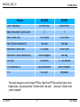
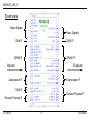
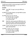
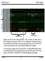
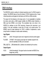
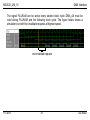
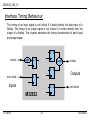
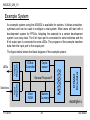
M32632_UM_10
M32632 V1.0
User's Manual
17.5.2015
1
Udo Möller
M32632_UM_10
Content
17.5.2015
Introduction .
.
.
.
.
. 3
Files .
.
.
.
.
.
.
. 5
Overview .
.
.
.
.
.
. 6
Basic Signals
.
.
.
.
. 7
General Purpose Interface.
. 10
DRAM Interface .
.
.
.
. 13
DMA Interface
.
.
.
. 19
Coprocessor Interface .
.
. 21
Interface Timing Behaviour.
. 23
Example System
.
.
.
. 25
Crossassembler .
.
.
.
. 28
2
.
Udo Möller
M32632_UM_10
Introduction
The M32632 is an implementation of the Series 32000 architecture of National
Semiconductor. It is 100% software compatible to the NS32532 CPU and NS32381
FPU. The implementation is written in Verilog.
The Series 32000 was a 32-bit microprocessor architecture of the 1980's. The basic
design concept was CISC : Complex Instruction Set Computer. Similar designs at
this time were the Motorola 68030 and the Intel 80386.
This user's manual describes the application of the M32632 inside of an FPGA
system. If you are interested in details of the Series 32000 architecture, for example
the instruction set, please read the datasheets of NS32532 and NS32381.
In an FPGA system the CPU is only one component of many other ones. Therefore
it is important that the CPU does not consume too much of the resources of an
FPGA. The M32632 requires some 15.400 logic elements, 13 18*18 multipliers and
32 memory blocks of 9 Kbits in a Cyclone IV FPGA from Altera. In a -6 speed grade
of the same FPGA the M32632 achieves 35 MHz.
The table on the next page compares some key characteristics of the original
NS32532 and the M32632.
17.5.2015
3
Udo Möller
M32632_UM_10
Introduction
Feature
Clock Frequency
Basic Instruction Cycle Count
Data Cache Size
Data Cache Associativity
Instruction Cache Size
Instruction Cache Associativity
TLB Size
TLB Associativity
FPU
NS32532
M32632
30 MHz max.
35 MHz min.
2
1
1024 bytes
8192 bytes
two way
two way
512 bytes
8192 bytes
direct mapped
two way
64 entries
2 * 256 entries
fully associative
direct mapped
NS32381
integrated
The clock frequency is for cheap FPGAs. High End FPGAs achive higher clock
frequencies. „fully associative“ is better than „two way“ , „two way“ is better than
„direct mapped“.
17.5.2015
4
Udo Möller
M32632_UM_10
Files
Top
1.
2.
3.
4.
5.
6.
7.
8.
9.
10.
11.
12.
13.
14.
15.
16.
The M32632 design is spread over 16 Verilog files (ending „.v“).
It is preferable to put them in one directory. See the list below for
file names and their content.
Modules
48 total
M32632.v
1
.
ICACHE.v
1
.
.
ICACHE_SM.v
2
.
STEUERUNG.v
1
.
.
DECODER.v
1
.
.
STEUER_MISC.v
5
.
DATENPFAD.v
1
.
.
I_PFAD.v
7
.
.
SP_FPU.v
4
.
.
DP_FPU.v
10
.
.
REGISTER.v
3
.
.
ADDR_UNIT.v
1
.
DCACHE.v
1
.
.
CACHE_LOGIK.v
6
.
.
ALIGNER.v
2
.
TOP_MISC.v
2
17.5.2015
2.Level 3.Level
5
Description
Top Level of M32632
Instruction Cache
Submodules for Instruction Cache
Global Control
Central Opcode Decoder
Submodules for Global Control
Data Path
Integer Data Path
Single Precision FP Data Path
Long Operations Data Path
Registers of Series 32000 Architec.
Address Generator Unit
Data Cache
Submodules for Data & Instr. Cache
Data Aligner
Submodules for Top Level
Udo Möller
M32632_UM_10
Overview
Basic Signals
Basic Signals
DMA IF
DMA IF
DRAM IF
DRAM IF
Inputs
Outputs
Coprocessor IF
Coprocessor IF
DMA IF
General Purpose IF
General Purpose IF
17.5.2015
6
Udo Möller
M32632_UM_10
Basic Signals
Input Signals
BCLK
„Basic Clock“ of the M32632 and the system.
MCLK
„Memory Clock“, used for the DRAM interface only, phase locked to
BCLK. It is best to use one PLL for generating both clocks.
BRESET
„Basic Reset“, active low.
NMI_N
„Nonmaskable Interrupt“, a high-to-low transition of this signal
requests a nonmaskable interrupt.
INT_N
„Interrupt“, a low level on this signal requests a maskable interrupt.
WRCFG
„Write Configuration“ is a static signal. If it is high, MCLK has to be
connected to the inverse of BCLK. If it is low, MCLK is an integer
multiple of BCLK.
The figure below is a screenshot of the ModelSim simulator and shows the
relationship between BCLK and MCLK. The rising edges are phase locked.
17.5.2015
7
Udo Möller
M32632_UM_10
Basic Signals
Output Signals
ILO
„Interlocked Operation“, the operations on the bus are interlocked.
This is used by the instructions SBITI and CBITI for multiprocessor
synchronization. (If someone will use 2 or more CPUs in one FPGA
please inform me!)
STATSIGS[7:0] „Statistic Signals Bus“, these 8 signals are monitoring bus activity
of the M32632. They are active high for one clock cycle for one event.
Their meaning is:
[0] Data access, internal from the data cache and external
[1] Data access from DRAM
[2] Data page table entry access
[3] Data write to DRAM
[4] Program access, internal from the instruction cache and external
[5] Program access from DRAM
[6] Program page table entry access
[7] Collision detected between data write and instruction cache
content
This signals may be connected to counters to watch M32632 activity.
On the next page the output of a program using this feature is
presented. Please note that every page table entry (PTE) access
includes two data memory reads. Therefore the program corrects the
number of data memory reads.
17.5.2015
8
Udo Möller
M32632_UM_10
Basic Signals
Collisions
:
160
Instruction PTE read
:
5600
Instruction memory read :
215312
Instruction read
:
144370288
Data write
:
30620416
Data PTE read
:
20048
Data memory read
:
4767520
Data read
:
54096000
Data Hit-Rate
: 91.19 %
Instruction Hit-Rate : 99.85 %
Elapsed Time :
12.372087 Sek.
Statistics of Linpack 100 benchmark on an M32632 system using NetBSD.
Output Signals, contd.
STATUS[3:0] „Status Bus“, this bus presents a status code for the general purpose
interface. Encodings are similar to the NS32532 status signals:
0000
idle
0001
idle, the M32632 is executing a WAIT instruction
0100
Interrupt acknowledge cycle
0110
End of interrupt cycle
1000
Program access cycle
1010
Data access cycle
All other codes are currently not used.
17.5.2015
9
Udo Möller
M32632_UM_10
General Purpose Interface
The general purpose interface is used for any bus operation until ENDRAM
becomes active. This is useful after reset when program execution starts at address
0. The first access goes normally to a boot ROM. Later the boot ROM is accessed
at a different location in the address space and the DRAM comes in at address 0.
This switch over is controlled outside of the M32632.
This interface has two limitations: it can not load the caches of the M32632 and is
not able to serve MMU operations. But this is not a serious drawback since every
FPGA system has a DRAM.
Input Signals
IO_READY „IO Ready“, the current operation (either a read or write) has finished.
This signal is active high. Holding it low will stretch the operation.
IO_Q[31:0]
„IO Data Read Bus“, the 32 bit wide data bus for any read data.
Output Signals
IO_RD
„IO Read“, if active high it requests a read operation.
IO_WR
„IO Write“, if active high it requests a write operation.
17.5.2015
10
Udo Möller
M32632_UM_10
General Purpose Interface
Output Signals, contd.
IO_A[31:0]
„IO Address Bus“, it contains the 32 bit wide byte address of the data
read or written.
IO_BE[3:0]
„IO Byte Enable Bus“, if active high the corresponding data has to be
written. The encoding is as follows:
IO_BE[0]
Byte 0 = IO_D[7:0]
IO_BE[1]
Byte 1 = IO_D[15:8]
IO_BE[2]
Byte 2 = IO_D[23:16]
IO_BE[3]
Byte 3 = IO_D[31:24]
IO_D[31:0]
„IO Data Write Bus“, the 32 bit wide bus contains the data to be
written.
On the next page a simulation run of multiple bus accesses is shown. The
instruction executed is a SBITI which activates the ILO signal. This instruction reads
one byte, modifies it (set one bit to „1“) and writes back the modified byte.
IO_BE[3:0] is set according to the byte address and STATUS[3:0] shows what is
ongoing on the general purpose interface.
17.5.2015
11
Udo Möller
M32632_UM_10
General Purpose Interface
A read access of the general purpose interface can be as short as one clock cycle.
But this is not possible if the access is directed to an FPGA memory block. The
boot ROM is such a memory block. It needs an extra clock cycle for its internal
operation: the address is sent to the memory and on the next rising edge the data is
provided to the interface. As far as I know this is true for all FPGAs of all vendors!
A write access can always be done in one clock cycle.
Program
access
17.5.2015
Data Read
access
12
Bus idle
Write
access
Program
access
Udo Möller
M32632_UM_10
DRAM Interface
The DRAM interface is the most complex interface of the M32632. The reason is
the different clocking. For example, on a DE0-nano board from Terasic, the M32632
is clocked with 35 MHz but the DRAM achieves 140 MHz. Transferring signals from
one clock domain to another clock domain is always a serious design issue. In the
M32632 the data cache and the instruction cache get the high frequency signals
from the DRAM controller. This direction is not seriously critical. The other direction
needs some special treatment. As already said the rising edges of BCLK and MCLK
must be synchronized with a PLL. Any output signal of the M32632 must be
synchronized to the falling edge of MCLK inside the DRAM controller first. See the
figure:
BCLK
Flipflop Output
Clock-to-output: 200 ps in Cyclone IV
MCLK
Flipflop Input
Setup time: 333 ps in Cyclone IV
3.5 ns
window width for an MCLK of 140 MHz
Using the rising edge of MCLK is unreliable because of clock jitter!
17.5.2015
13
Udo Möller
M32632_UM_10
DRAM Interface
Inside the M32632 the rising edge of MCLK is used. Therefore output signals of the
DRAM controller must be transfered from falling edge logic to rising edge flipflops.
The cache line size of the M32632 is 16 bytes. The cache line is always filled with a
burst access of the DRAM. 4 double words (Dword) of 4 bytes each are read
without any interruption. The first Dword read is always the one which the M32632
requests. To build an efficient DRAM controller it is important to know the possible
Dword sequences from the M32632 point of view:
First Dword address: 0
possible next Dword address: 1
1
0 or 2 (!)
2
3
3
2 (or 0 = not critical)
The case „first Dword address = 1“ is challenging. A DRAM can be configured to a
burst mode of „sequential“ or „interleave“. For the DRAM of the DE0-nano board
two column accesses for one burst with mode „interleave“ is the best choice.
The write behaviour of the data cache of the M32632 is „write through“. This means
that every write data is instantly written to the DRAM. Another method would be
„write back“. Only the cache is updated but the external memory is updated later.
The advantage of this method (little more performance) is not worth the additional
effort (DRAM data not current when DMA occurs).
17.5.2015
14
Udo Möller
M32632_UM_10
DRAM Interface
The M32632 selects the DRAM in the address space between 0 and 0x0FFF_FFFF
(256 MByte). This can be changed on request.
Input Signals
ENDRAM
„Enable DRAM“, if this signal is active high the DRAM can be
accessed.
DC_MDONE „Data Cache Memory Read Done“, active high if M32632 can proceed
(synchronized to BCLK).
DC_WCTRL[2:0]
[0]
[1]
[2]
ENWR
„Data Cache Write Control Bus“:
if active high access is not cacheable
write pulse for data cache RAM
write pulse for first Dword
„Enable Write“, active high, goes low if the DRAM interface cannot
accept another write request. The M32632 ignores this signal if a write
targets the same cache line as the last write (synchronized to BCLK).
IC_MDONE „Instruction Cache Memory Read Done“, active high if M32632 can
proceed (synchronized to BCLK).
IC_WCTRL[2:0]
[0]
[1]
[2]
17.5.2015
„Instruction Cache Write Control Bus“:
if active high access is not cacheable
write pulse for instruction cache RAM
write pulse for first Dword
15
Udo Möller
M32632_UM_10
DRAM Interface
Input Signals, contd.
WAMUX
„Write Address Muliplexer“, if this signal is active high it passes the
write address to the data cache RAM.
WADDR[11:2]
„Write Address Bus“, WADDR[3:2] counts the Dword address,
WADDR[11:2] is taken either from DRAM_ADR[11:2] or
IDRAM_ADR[11:2]. The Dword counter is in the DRAM controller.
DRAM_Q[31:0]
„DRAM Data Out Bus“, all bits must be valid.
Ouput Signals
DC_ACC
„Data Cache Access“, if active high the data cache is requesting read
data.
DC_WR
„Data Cache Write“, if active high the data cache is requesting a write
operation.
DRAM_ADR[27:0]
[0]
[1]
[3:2]
„Data Cache Address Bus“, used for read and write access:
don't care
if this signal is active low the access is not cacheable, either
suppress DWCTRL[1] or set DWCTRL[0] to active high
first Dword to read
DRAM_DI[35:0] „DRAM Data In Bus“, the write data to the DRAM:
[31:0] Data
[35:32] Byte Enable, [35]=[31:24],[34]=[23:16],[33]=[15:8],[32]=[7:0]
17.5.2015
16
Udo Möller
M32632_UM_10
DRAM Interface
Ouput Signals, contd.
IC_ACC
„Instruction Cache Access“, if active high the instruction cache is
requesting read data.
IDRAM_ADR[27:0]
[0]
[1]
[3:2]
„Instruction Cache Address Bus“, used only for read access:
don't care
if this signal is active low the access is not cacheable, either
suppress IWCTRL[1] or set IWCTRL[0] to active high
first Dword to read
Another reason why the DRAM interface is build like this is that in principle the
accesses of the data cache and the instruction cache can be overlapped. This is
possible because the DRAM has build-in capabilities for two operations in parallel:
the row access and the column access. But to build a controller which is able to use
this at high frequencies is not an easy task …
Please note that IC_MDONE comes one BCLK clock cycle later then DC_MDONE.
This is necessary to cover all possible access cases of a program flow.
On the next page a simulation output of a read and write operation at the DRAM
interface of the M32632 is presented.
17.5.2015
17
Udo Möller
DRAM Interface
MCLK
BCLK
M32632_UM_10
Read Access
Write Access
Please note that the third Dword (WADDR = 0a2) is written one clock cycle of
MCLK before the rising edge of BCLK. This is necessary for the memory block of
the cache RAM to read the correct next data (either from 0a0 or 0a2). The first write
is not critical because the data is read inside the M32632 from a register.
The write access requires one clock cycle of BCLK. The signal ENWR goes inactive
on the falling edge of BCLK eventually delaying the next write access. One of two
buffers is now written to the DRAM. If this is done ENWR goes active again.
17.5.2015
18
Udo Möller
M32632_UM_10
DMA Interface
The NS32532 is able to continue its internal operations even if a HOLD request is
ongoing. The M32632 does not have this feature. If HOLD becomes active, it stops
internal operations and signals its hold status via HLDA to a DMA controller.
The reason for this behaviour is the large cache. It is not acceptable to invalidate
the whole cache when a DMA request modifies the DRAM content (therefore a
DMA read from DRAM is not critical). This invalidation has to be done in the
NS32532 by software via the CINV instruction. However this instruction is not
optimal. It can only invalidate a cache line (16 byte) or the whole cache. The
M32632 uses the same behaviour for CINV. In addition it implements a cache
snoop function in hardware to realize cache coherency.
Input Signals
HOLD
„Hold“, if this signal is active low it request bus free for another agent.
FILLRAM
„Fill RAM“, if this signal is active high an invalidate request for the
cache line address on DMA_AA is executed.
DMA_AA[27:4]
„DMA Address Bus“, address to be checked by the caches.
Output Signals
HLDA
17.5.2015
„Hold Acknowledge“, this signal is active low when the M32632 has
stopped any activity.
19
Udo Möller
M32632_UM_10
DMA Interface
The signal FILLRAM can be active every second clock cycle. DMA_AA must be
valid during FILLRAM and the following clock cycle. The figure below shows a
simulation run with five invalidate requests at highest speed.
one invalidate request
17.5.2015
20
Udo Möller
M32632_UM_10
Coprocessor Interface
The coprocessor capability of the Series 32000 is used by National Semiconductor
itself. The NS32381 FPU is an external coprocessor. Therefore instructions using
this coprocessor have a lot of communication overhead. In contrast the M32632
has the floating point unit integrated and avoids the communication overhead. The
result is much faster operation.
Nevertheless it is useful to add the external coprocessor capability also to the
M32632. It provides an easy way to expand the functionality of the CPU. Not
everybody will like the idea of manipulating the core itself.
The M32632 V1.0 is able to execute the CCV0, CCAL0, CCAL1, CCAL2, CCAL3,
CMOV0, CMOV1 and CMOV2 custom instructions.
Input Signals
COP_DONE „Coprocessor Done“, if this signal is active high for one clock cycle it
signals the completion of the requested operation.
COP_IN[63:0]
„Coprocessor Data Input Bus“, this bus is connected to the data
output port of the coprocessor. A quad word is transfered over bits
[63:0], a double word over bits [63:32], a word over bits [47:32] and a
byte over bits [39:32].
17.5.2015
21
Udo Möller
M32632_UM_10
Coprocessor Interface
Output Signals
COP_GO
„Coprocessor Go“, if this signal is active high the coprocessor starts
the requested operation.
COP_OP[23:0] „Coprocessor Opcode Bus“, this bus contains the three opcode
bytes. Please look at the datasheet of the NS32532 for details of the
instruction formats.
COP_OUT[127:0]
„Coprocessor Data Output Bus“, this bus is connected to the
data input port of the coprocessor. It can hold two 64 bit quad word
operands and is static throughout the coprocessor operation.
The location of data depends on the operation:
Bits
127...96-95....64-63....32-31.....0
One Double Word
XxXxXxXx_B3B2B1B0_XxXxXxXx_XxXxXxXx
One Quad Word
XxXxXxXx_B7B6B5B4_XxXxXxXx_B3B2B1B0
Two Double Words
XxXxXxXx_B3B2B1B0_XxXxXxXx_b3b2b1b0
Two Quad Words
B7B6B5B4_B3B2B1B0_b7b6b5b4_b3b2b1b0
Bi = first operand, bi = second operand, Bi/bi = byte i
17.5.2015
22
Udo Möller
M32632_UM_10
Interface Timing Behaviour
The timing of an input signal is not critical if it feeds directly the data input of a
flipflop. The timing of an output signal is not critical if it comes directly from the
output of a flipflop. This chapter describes the timing characteristic of each input
and output signal.
D Q
critical
Logic
D Q
Logic
D Q
not critical
D Q
Inputs
D Q
critical
Outputs
not critical
M32632
17.5.2015
23
Udo Möller
M32632_UM_10
Interface Timing Behaviour
Input Signals
Not relevant:
BCLK, MCLK, WRCFG
Not critical:
BRESET, NMI_N, INT_N, IO_READY, IO_Q[31:0], HOLD
Weakly critical, should be driven by output of flipflop:
IC_MDONE, DC_MDONE, ENWR, ENDRAM, FILLRAM,
DMA_AA[27:2]
Strongly critical, must be driven by output of flipflop:
IC_WCTRL[2:0], DC_WCTRL[2:0], WAMUX, WADDR[11:2],
DRAM_Q[31:0], COP_DONE, COP_IN[63:0]
Output Signals
Not critical:
STATSIGS[7:0], IC_ACC, IDRAM_ADR[27:0], DC_WR, DC_ACC,
DRAM_ADR[27:0], DRAM_DI[35:0], IO_RD, IO_WR, IO_A[31:0],
IO_BE[3:0], IO_DI[31:0], COP_GO, COP_OP[23:0]
Weakly critical, should not feed deep logic trees:
STATUS[3:0], ILO, HLDA, COP_OUT[127:0]
17.5.2015
24
Udo Möller
M32632_UM_10
Example System
An example system using the M32632 is available for starters. It allows simulation,
synthesis and can be used to configure a real system. Most users will start with a
development system for FPGAs. Adopting the example to a certain development
system is an easy task. The 8 bit input port is connected to some switches and the
8 bit output port is connected to some LEDs. The program of the example transfers
data from the input port to the output port.
17.5.2015
Coprocessor
General Purpose IF
Boot
ROM
Statistic
Counters
25
DRAM
Emulator
IO Bus
Controller
M32632
Switches
Input
Register
LEDs
Output
Register
The figure below shows the block diagram of the example system.
example.v
Udo Möller
M32632_UM_10
Example System
The following files are used for the example system:
1. example.v
2. example_mods.v
3. example_tb.v
4. example.sdc
the top module for synthesis containg the M32632
the submodules of the example system
the test bench for simulating the example system
the timing requirements file
The file example.sdc definies the timing for the example system. The most important
definition is for the clock cycle time. Current setting for the clock signal is 30 ns with the
falling edge at 15 ns. This setting should be pass for every modern FPGA. The file
example.qsf is used by Altera's Quartus software to setup a project.
Each system using the M32632 contains at least two other functional blocks: the IO
bus controller and the boot ROM. The „IO Bus Controller“ does the following:
1. selects different locations for writing based on their addresses
2. multiplexes the incoming data busses for the M32632
Please note : there is no tri-state bus inside a FPGA!
3. manages the switch over between boot ROM and DRAM
4. generates IO_READY and a clean reset
A boot ROM is a memory which stores the first instructions after reset for a CPU.
The other blocks are optional:
1. DRAM Emulator: almost every development board has a standard DRAM on it. But
there are many standards: SDRAM, DDR, DDR2, … To avoid building a DRAM
controller a DRAM emulator is provided for a quick start.
17.5.2015
26
Udo Möller
M32632_UM_10
Example System
The DRAM emulator uses internal memory blocks of the FPGA. The example
implements 16 kBytes. If your FPGA has enough capacity the memory can be
enlarged. But 16 kBytes should be sufficient even for some experiments with virtual
memory.
2. Coprocessor: as an example the coprocessor implements a byte swap instruction. In
a double word or a quad word the byte order is reversed.
3. Statistic Counters: these counters are connected to the STATSIGS[7:0] bus of the
M32632. In this way, the CPU can monitor its own activity. If there are only LEDs
available showing this information may be difficult. A small LCD display is a better
choice.
4. Input Port: the input port is connected to any switches on the development board. If
there are more than 8 switches one can read a word instead of a byte from the port. A
two stage synchronizer is provided to avoid any metastability inside the FPGA system.
5. Output Port: the output port is connected to any LEDs on the development board. As
with the input port its width depends on the number of LEDs.
A nice application for starters is a measurement system for reaction times. One of
multiple LEDs is activated and a certain button or switch must be pressed. The time
between these events is measured and displayed. Another application is a clock based
on an interrupt every second. If this is boring for you, develop a DRAM controller for
your board ...
17.5.2015
27
Udo Möller
M32632_UM_10
Crossassembler
The crossassembler „ans32k“ is used on a Windows PC to generate assembler
programs for the M32632. The output can be used in simulation, configuration and
in real systems. The syntax is similar to other assembly languages. Another way of
generating programs is to use the gnu tool chain. It provides crossassembling and
crosscompiling. But you have to use old versions of gnu which still support Series
32000! „ans32k“ is used in a command shell:
C:\ … \ans32k filename <outfile> <-list> <-code> <-mif> <-n>
Arguments and options (<...>) are:
filename
the name of the input file.
<outfile>
other name for the output file, must be the 2. argument. Default is
„boot_rom.txt“, for -mif it is „bootcode.mif“.
<-list>
this option generates a list file containing the address of each
instruction. The name of the file is „filename.LST“.
<-code>
this option adds the binary code of the instruction to the list file.
<-mif>
change the output format to Altera mif format instead of simple hex.
<-n>
size of the target ROM, valid values for n are 1,2,4 and 8 kBytes.
Default is 1 kBytes. Datawidth is always 32 bit.
17.5.2015
28
Udo Möller