1
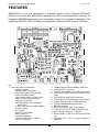
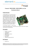
D O C - 0 4 3 9 - 0 1 0 ,
R E V . D
M54451EVB
Development Board for Freescale MCF54451 MCU
Hardware User Manual
PRELIMINARY
ٛ Axiom Manufacturing • 1226 Exchange Drive • Richardson, TX 75081
Email: [email protected] Web: http://www.axman.com ٛ
M 5 4 4 5 1 E V B
U S E R
M A N U A L
0 1 / 1 5 / 0 9
CONTENTS
CAUTIONARY NOTES .......................................................................................................................... 2
TERMINOLOGY ..................................................................................................................................... 2
FEATURES ............................................................................................................................................... 3
REFERENCE DOCUMENTATION ...................................................................................................... 4
M54451EVB STARTUP........................................................................................................................... 4
M54451EVB HARDWARE SUMMARY ............................................................................................... 5
MCU APPLICATION .................................................................................................................................. 5
SWITCH SUMMARY ................................................................................................................................... 5
INDICATOR SUMMARY .............................................................................................................................. 6
EXTERNAL CONNECTION SUMMARY......................................................................................................... 6
OPTION JUMPER SUMMARY ...................................................................................................................... 7
HARDWARE APPLICATION ........................................................................................................................ 8
Memory................................................................................................................................................. 8
System Clocks....................................................................................................................................... 8
Stereo Audio CODEC........................................................................................................................... 8
10/100TX Ethernet Port – J1 ............................................................................................................... 9
USB Mini A/B OTG Port – J2 .............................................................................................................. 9
FXO and FXS Ports.............................................................................................................................. 9
EVB POWER SUPPLIES ..................................................................................................................... 9
EVB Development Ports....................................................................................................................... 9
EVB OPERATION ................................................................................................................................. 10
EVB POWER SELECTION AND OPTIONS ........................................................................................... 10
Power Jack (PWR) ............................................................................................................................. 10
Power Over Ethernet (POE) Supply .................................................................................................. 10
POE_ON Indicator............................................................................................................................. 10
PWR_SEL Option............................................................................................................................... 10
+5V Indicator..................................................................................................................................... 11
TB1 - +5V and Ground Access .......................................................................................................... 11
F1 - Fuse ............................................................................................................................................ 11
ON_OFF Switch................................................................................................................................. 11
+3.3V, +1.8V, and +1.5V Indicators ................................................................................................. 11
JP13, JP14, JP15 - U1 Power Enable ............................................................................................... 11
EVB START-UP AND OPTIONS.......................................................................................................... 12
BOOT_0, BOOT_1 Options ............................................................................................................... 12
JP3 – Serial Flash Memory Select Enable......................................................................................... 12
RESET Switch..................................................................................................................................... 12
RESET Indicator ................................................................................................................................ 12
1
M 5 4 4 5 1 E V B
U S E R
M A N U A L
0 1 / 1 5 / 0 9
Cautionary Notes
1) Electrostatic Discharge (ESD) prevention measures should be applied whenever handling
this product. ESD damage is not a warranty repair item.
2) Axiom Manufacturing reserves the right to make changes without further notice to any
products to improve reliability, function or design. Axiom Manufacturing does not assume
any liability arising out of the application or use of any product or circuit described herein;
neither does it convey any license under patent rights or the rights of others.
3) EMC Information on the M54451EVB board:
a) This device complies with Part 15 of the FCC Rules. Operation is subject to the following
two conditions:
1) This device may not cause harmful interference, and
2) This device must accept any interference received, including interference that may
cause undesired operation.
b) This product as shipped from the factory with associated power supplies and cables, has
been tested and meets with requirements of CE IT Equipment CLASS A product.
c) This product is designed and intended for use as a development platform for hardware or
software in an educational / professional laboratory.
d) In a domestic environment this product may cause radio interference in which case the
user may be required to take adequate prevention measures.
Terminology
This development board applies option selection jumpers. Terminology for application of the
option jumpers is as follows:
Jumper on, in, or installed = jumper is a plastic shunt that fits across 2 pins and the
shunt is installed so that the 2 pins are connected with the shunt.
Jumper off, out, or idle = jumper or shunt is installed so that only 1 pin holds the shunt,
no 2 pins are connected, or jumper is removed. It is recommended that the jumpers be
placed idle by installing on 1 pin so they will not be lost.
Signal names in this document that are followed by an asterisk (*) denote an active-low signal.
2
M 5 4 4 5 1 E V B
U S E R
M A N U A L
0 1 / 1 5 / 0 9
FEATURES
M54451EVB is a low cost development or evaluation system for the Freescale MCF54451
ColdFire® microcontroller. EVB features are aimed at VOIP or similar application solutions. An
integrated USB BDM development port is provided on board for development assistance. The
supporting MCF52211 MCU provides an I/0 application coprocessor with a device USB port.
♦
♦
♦
♦
♦
Features:
♦ MCF54451 MCU, 256 MAPBGA
* 240Mhz operation
* 32K Byte single cycle SRAM
* DDR, DDR2, Mobile DDR Controller
* 16 channel DMA Controller
* XBS Crossbar Switch w/ multiple ports
* USB OTG Controller w/ ULPI bus
* Integrated 10/100 FEC
* SPI w/DMA (DSPI), IIC, and SSI/I2S
Serial Ports
* 2 UART Serial Ports with DMA capability
* 4 Interrupt Inputs
* 4 PIT timers
* 4 32 bit Timers w/ DMA
* BDM / JTAG Port
* Serial Boot capability
* Internal Oscillator w/ PLL clocking
* 3.3V / 1.5V operation
♦
♦
♦
♦
♦
♦
♦
♦
♦
♦
3
128MByte Mobile DDR
16MByte Parallel flash and 8MByte Serial flash
USB OTG PHY on ULPI bus
10/100TX Port on RMII bus w/ POE power supply
Stereo Audio CODEC w/ Line I/O and MIC 3.5mm
Jacks
FXS CODEC w/ DAA Phone Connection
FXO CODEC w/ DAA Subscriber Line Connection
Support MCF52211 MCU w/ USB connection
On-Board USB BDM Development Port
SD Card connector
RESET and ABORT (IRQ7) push switches
8 User and 2 10/100TX Status Indicators (LED)
MCU I/O Port Connectors, 2 x 50 pins
External BDM / JTAG Port, 26-pin development
port
Regulated +3.3V / 1.8V / 1.5V power supplies w/
indicators
M 5 4 4 5 1 E V B
U S E R
M A N U A L
0 1 / 1 5 / 0 9
Kit content: Supplied with 10/100 Ethernet cable, 5VDC Wall Adapter Power Supply,
USB A/B cables, Quick start and Support CD media.
Specifications:
Board Size 5 x 6 inches w/ 4 corner mounting holes
Power Input: +4.5 - +5.5VDC, 5.0VDC typical
POE supply Input: 48V typical, 5V output
Current Consumption: 300ma typical @ 5VDC input
The M54451EVB is provided operating a demonstration application. Refer to the M54451EVB
Quick Start Guide for more information on default operation. The EVB kit is plug in and play as
delivered with a global wall adapter power supply, cables, support CD, and example software.
Additional hardware and software development tools are available, but not required.
Reference Documentation
The following documents should be referenced when developing with the M54451EVB. These
documents are available on the MCF54451 and M54451EVB web pages
(http://www.freescale.com/coldfire).
M54451EVBUM
– This user manual.
MCF54455RM
– MCF54451 Device Reference Manual
CFPRM
– ColdFire Programmers Reference Manual with instruction set
M54451EVB_SCH_D – M54451EVB board schematics
M54451EVB Startup
Follow these steps to connect and power on the board
1) Carefully unpack the M54451EVB and observe ESD preventive measures while handling
the M54451EVB development board.
2) Review the Quick Start guide and option settings on the EVB.
3) Install supporting software prior to connecting the USB ports. Review the support CD(s)
and copy documentation or install software as wanted.
4) Connect necessary cables between host PC and EVB board prior to applying power to the
EVB.
5) Apply power to the development board by installing the +5.0VDC wall plug power supply
between a wall outlet and the PWR Jack on the board. The +5VDC indicator should be
ON. Set the ON / OFF switch to the ON position. The EVB +5, 3.3V, 1.8Vand 1.5V
voltage indicators should turn on at this time. Note: PWR_SEL = PWR setting default, see
the POE section for operating the POE supply.
6) Follow the Quick Start for preloaded application operation or launch development tools.
7) The board is ready to use now.
4
M 5 4 4 5 1 E V B
U S E R
M A N U A L
0 1 / 1 5 / 0 9
M54451EVB Hardware Summary
The M54451EVB board provides an enhanced development or evaluation platform for the
MCF54451 microcontroller. Following are descriptions of the primary components and EVB
application.
MCU Application
The MCF54451 is applied with features supporting the many interfaces available on the
device. Also provided is a supporting MCF52211 MCU operating as a support processor.
Following is a summary of the applied hardware:
•
USB OTG Mini A/B port (J2) supported by MCF54451 ULPI bus and a USB3300 ULPI PHY
device.
•
10/100Tx Ethernet port supported by MCF54451 FEC0 in RMII mode, KSZ8041 PHY, X1
50Mhz clock, Connector J1, and Power Over Ethernet (POE) power supply input.
•
Mobile DDR Ram 64M x 16 supported by MCF54451 SDRAM Controller.
•
Parallel Flash Memory 8M x 16 supported by MCF54451 Flex Bus (28F128P33).
•
Serial Flash Memory 8M byte supported by MCF54451 DSPI / Serial Boot facility and the
MCF52211 support MCU.
•
SDCARD connector supported by MCF54451 DSPI.
•
Telephony FXS and FXO ports supported by MCF54451 SSI and DSPI, and the Si3210
and Si3050 integrated solutions.
•
Stereo Audio CODEC (TLV320AC23) supported by MCF54451 SSI and DSPI.
•
Support MCU (MCF52211) with USB client port, and DSPI or development port access to
the MCF54451.
•
Eight Indicators for application use.
Switch Summary
Indicator
ON / OFF
RESET
U4_RESET
ABORT
Purpose
EVB power on and off
Reset MCF54451 (U1)
Reset MCF52211 (U4)
NMI /IRQ7 MCF54451
Operation Notes
Enables EVB voltage regulators when ON.
Applies MCF54451 RSTIN* signal active.
Applies MCF52211 RSTIN* signal active.
Applies MCF54451 IRQ7/NMI signal low
(application must enable and support).
5
M 5 4 4 5 1 E V B
U S E R
M A N U A L
0 1 / 1 5 / 0 9
Indicator Summary
Indicator
RESET
U4_RESET
+1.5V
+1.8V
+3.3V
+5V
POE_ON
LED1 – 4
LED5 – 8
LNK_ACT
SPD
D501
D502
Purpose
Reset Indication (Red)
Reset Indication (Red)
+1.5V Voltage (Green)
+1.8V Voltage (Green)
+3.3V Voltage (Green)
+5V Voltage (Green)
POE +5V Voltage (Green)
User / App (Green)
User / App (Green)
Ethernet Status (Green)
Ethernet Status (Green)
Embedded BDM Status (Green)
Embedded BDM Status (Yellow)
Indication Notes
U1 - MCF54451 RESETOUT* is active.
U4 - MCF52211 RSTOUT* is active
Power supply 1.5V is present.
Power supply 1.8V is present.
Power supply 3.3V is present.
+5V input supply is present.
+5V from POE supply is available.
U4: Port AN0 – 3 is high level.
U1: Port DT0-3IN is high level.
10/100Tx PHY has Link or Activity
10/100Tx PHY is in 100Mbs mode.
Target power detected (D502 must be on).
J501 USB connected, BDM is active.
External Connection Summary
Connector
J1
J2
Purpose
10/100Tx Ethernet /
POE
USB OTG Mini A/B
J3
J501
PWR (Jack)
TB1 (not
populated)
F1 Fuse
LINE_IN
U4 USB-B
BDM USB-B
External +5V input
Alternate +5V input
or output
5 x 20mm fuse clips
Stereo CODEC input
LINE_OUT
Stereo CODEC
output
Stereo CODEC input
FXS Phone I/O
FXO Office Line I/O
SD memory card or
SDIO device I/O
Signal access
MIC_IN
PHONE
LINE
SDCARD
IO_PORT1 /
2
BDM_PORT
U4_BDM
J4
J5
J6
U1 External BDM
U4 External BDM
ULPI Bus access
ULPI Bus access
SSI Bus access
Application Notes
Applies MCF54451 Ethernet connection and POE
power supply input.
Applies MCF54451 ULPI type USB 2.0 host or client
port.
MCF52211 USB client port for support applications.
Embedded USB BDM port.
Primary +5V input application to power the EVB.
Alternate connection to +5V input supply.
2A fuse connection for primary +5V supply.
3.5mm Audio input jack (Line-In and Line-Out looped
back if plug is not installed).
3.5mm Audio output jack (Line-In and Line-Out
looped back if plug is not installed).
3.5mm Microphone input jack.
RJ11 Phone / Handset connection.
RJ11 Office Subscriber Line connection.
SDCARD or SDIO connection. Operates in simple
mode under MCF54451 control.
MCF54451 Flex Bus and GPIO access ports.
MCF54451 External BDM Port. (Do not apply at same
time as the Embedded USB BDM.)
MCF52211 BDM port for application loading.
MCF54451 ULPI bus signal access.
MCF54451 ULPI bus signal access.
MCF54451 SSI / I2S bus signal access.
6
M 5 4 4 5 1 E V B
U S E R
M A N U A L
0 1 / 1 5 / 0 9
Option Jumper Summary
Option
PWR_SEL
Purpose
+5V input
source select
ULPI clock
enable
Default
PWR
Application Notes
Selects PWR jack / TB1 or POE supply input
1-2
Select
MCF54451 Boot
mode
MCF54451
BDM Port Mode
BDM_PORT
Mode
MCF52211
U4_BDM Port
Mode
U4 SPI Select
Installed
1-2 position applies 40Mhz USB ULPI clock to
MCF54451 USB clock input. 2-3 position
removes clock.
Both Installed = Flex Bus / parallel Flash
default.
Both open / idle = Serial Boot Mode.
Open / Idle = MCF54451 BDM Mode
Installed = MCF54451 JTAG Mode
1-2 Position selects BDM Port JTAG mode.
2-3 Position selects BDM Port BDM mode.
Installed = MCF52211 BDM Mode
Open / Idle = MCF52211 JTAG Mode
Serial Flash
Select enable
Stereo CODEC
SSI enable
+VDC enable
SDCARD Select
Installed
Installed
JP12
Stereo CODEC
Select enable
10/100 PHY
IRQ
FXO CODEC
Select enable
FXS CODEC
Select enable
FXO/FXS IRQ1
Enable
U4_BDM Mode
JP13
MCF54451 3.3V Installed
JP14
MCF54451 1.5V Installed
JP15
MCF54451 1.8V Installed
USB_CLK
BOOT 0 /1
JTAG_EN
BDM_MODE
JP1
JP2
JP3
JP4
JP5
JP6
JP7
JP8
JP9
JP10
JP11
U4_MODE1/2 U4 Application
Idle
2-3
Installed
1-2
Installed
Installed
1-2
Installed
Installed
Installed
Installed
Open
Installed
1-2 = U4 / MCF52211 QSPICS0 select on
MCF54451 DSPICS0 signal.
2-3 = U4 / MCF52211 QSPICS0 select on
MCF54451 DSPICS1 signal.
MCF54451 DSPICS1* / Serial Boot chip select
enabled to the serial flash.
Enable CODEC SSI Bus data output.
Enable EVB +5V to FXS port = +VDC supply
1-2 = MCF54451 DSPICS0 signal selects
SDCARD.
2-3 = MCF54451 DSPICS1 signal selects
SDCARD.
MCF54451 DSPICS5 select enabled to the
Stereo CODEC.
MCF54451 IRQ3 input assigned to 10/100
Ethernet PHY.
MCF54451 DSPICS3 select enabled to the
FXO CODEC.
MCF54451 DSPICS2 select enabled to the FXS
CODEC.
MCF54451 IRQ1 input assigned to the
FXO/FXS CODEC’s and DAA’s.
Option not installed, U4_BDM Port = BDM
mode.
MCF54451 +3.3V supply enable, ALWAYS
Install
MCF54451 +1.5V core supply enable,
ALWAYS Install
MCF54451 +1.8V SDRAM supply enable,
ALWAYS Install
U4 application support, refer to application.
7
M 5 4 4 5 1 E V B
U S E R
M A N U A L
0 1 / 1 5 / 0 9
Hardware Application
Memory
The internal MCF54451 device SRAM, EVB Mobile DDR memory, EVB Parallel Flash memory,
EVB Serial Flash memory, and EVB SDCARD connections provide the development and
application memory banks. The MCF54451 provides internal 32K bytes of high speed SRAM
for DMA and Cache memory space. Refer to the MCF54455 device user guide for device
details.
The MCF54451 SDRAM controller is dedicated to U2, the EVB 128MByte Mobile DDR Ram
memory. The Mobile DDR ram device is a Micron MT46H64M16.
MCF54451 Flex Bus application on the EVB is a single 16MByte parallel flash (Ny28F128P33)
assigned to chip select FB_CS0*. The flash may be applied as application program and boot
memory or storage memory. The Flex Bus may be applied as GPIO at the I/O PORT
connectors if the flash application is not desired. Refer to EVB Start-up Options for configuring
the Boot and memory selection.
Serial Flash of 8MBytes is provided for DSPI access or as an optional boot memory device.
SDCARD connection is provided for memory expansion or addition of peripheral features.
System Clocks
The EVB provides the MCF54451 a 24MHz crystal oscillator reference for typical application
operation at 240Mhz. The Mobile DDR ram operates at 120MHz and the Flex Bus at 60Mhz
maximum clock rate. USB and Ethernet clock rates and EVB application are provided in the
respective sections of this manual.
SSI CLOCK: The Y5 Crystal location provides default 12.288Mhz clock frequency for the SSI
clock input to the MCF54451 IRQ4 / SSI clock pin. This frequency may be changed by
replacing the crystal with a similar 20pf parallel load type with a frequency between 8 and
16Mhz. Refer to the MCF54451 SSI reference manual for more details on operation.
Stereo Audio CODEC
The EVB provides a TLV320AC23 Stereo Audio CODEC for stereo audio applications via the
MCF54451 SSI / I2S serial bus. The CODEC is supported by three 3.5mm (1/8”) jacks for
Microphone, Line IN and Line OUT audio connections. Note that the Stereo CODEC may not
operate at the same time as the FXS/FXO telephony CODECs. Refer to the demonstration
application for operation details.
8
M 5 4 4 5 1 E V B
U S E R
M A N U A L
0 1 / 1 5 / 0 9
10/100TX Ethernet Port – J1
The 10/100TX Ethernet physical interface connection and the Power Over Ethernet (POE)
supply input are applied by RJ45 connector J1. Port configuration applies the MCF54451 Fast
Ethernet controller (FEC) and KSZ8041 PHY operating in RMII mode. The coupling
transformer T1 provides port isolation and the input power path to the POE supply. Clock
oscillator X1 provides the 50MHz clock source for the PHY and FEC communication.
USB Mini A/B OTG Port – J2
This USB 2.0 host or device mode port is provided by the MCF54451 ULPI bus and USB3300
PHY device. MCF54451 USB port signal pins USBD- / USBD+ are not applied by the EVB
and are provided on the I/O PORT connectors. The ULPI PHY applies a 24Mhz reference
crystal oscillator to generate the 40Mhz ULPI bus clock. Host mode operation is supported by
device power output switch, U8.
FXO and FXS Ports
The EVB provides a FXO Line interface and a FXS Station interface with integrated CODEC’s
and DAA’s. These ports are to be considered development application use only and are not
qualified to be permanently attached to a public or private network. The FXS Phone / Station
port will provide up to 48V phone battery supply and ringing voltages. The FXO Line / Office
port accepts a standard subscriber line interface and ringing input signals.
EVB POWER SUPPLIES
The EVB provides three regulated power supplies from a regulated +5VDC input supply. The
+5V input is provided by the PWR Jack or Power Over Ethernet (POE) power supply. Both
power supplies may be powered on at the same time but only one may be applied to power the
EVB board. The PWR_SEL option jumper selects which power supply will operate the EVB
board. Default application is for regulated +5VDC to be applied by external connection to the
Power Jack (PWR). The ON _OFF switch enables the regulated 3.3V, 1.8V and 1.5V supplies
to the EVB circuits.
EVB Development Ports
The EVB provides an embedded USB BDM and external BDM_PORT for the MCF54451.
Support processor U4 (MCF52211) has a U4_BDM_PORT for application loading.
9
M 5 4 4 5 1 E V B
U S E R
M A N U A L
0 1 / 1 5 / 0 9
EVB OPERATION
EVB POWER SELECTION and Options
Power Jack (PWR)
The Power Jack provides the default +5VDC power input to the board. The jack accepts a
standard 2.0 ~ 2.1mm center barrel plug connector (positive voltage center) to provide the +5V
supply of +4.5 to +5.5 VDC (+5.0VDC typical).
+Volts, 2mm center
Power Over Ethernet (POE) Supply
The POE supply (Freescale MC34670) input is from the J1 Ethernet connector. A POE
enabled Ethernet switch or host equipment provides the supply for this input. The POE_ON
indicator will be ON if this supply is available. This is an isolated type supply, test pads +VE
and –VE must not be grounded by test equipment or EVB signal connections, damage may
occur.
POE_ON Indicator
The POE_ON indicator will light if the Ethernet POE supply is powered and operating.
PWR_SEL Option
PWR_SEL option jumper provides selection of the PWR Jack input or POE supply input to
power the EVB board +5VDC source. Default position is for PWR jack to provide power.
PWR_SEL
PWR Jack Input
PWR_SEL
POE Supply Input
10
M 5 4 4 5 1 E V B
U S E R
M A N U A L
0 1 / 1 5 / 0 9
+5V Indicator
The +5V indicator will be ON if a +5V source is available from the PWR Jack or POE supply.
The PWR_SEL option must also be installed to select the correct input supply. If a +5V supply
is provided and the +5V indicator is not ON, check fuse F1 and review for power issues.
TB1 - +5V and Ground Access
TB1 is not populated by default. The TB1 position and PCB pads provide access to the same
connections as the PWR Jack. +5V applied at the PWR Jack may be accessed at the TB1
location. TB1 location may apply a +5V supply to the EVB board if the PWR Jack is not
applied.
F1 - Fuse
F1 is populated by a 5x20mm 2Amp fuse. The fuse is applied between the +5V input from the
PWR jack or POE supply and the EVB board circuits. If +5V or POE supply is applied to the
EVB and the +5V Indicator is not ON, the fuse should be checked and replaced if required.
Fuse failure may indicate an EVB failure, user should review connections and application for
possible cause.
ON_OFF Switch
The ON_OFF switch provides power On and Off control for the EVB 3.3V, 1.8V and 1.5V
voltage regulators. All voltage indicators should be ON with the switch in the ON position
(power applied).
ON
OFF
+3.3V, +1.8V, and +1.5V Indicators
These indicators will be ON if the associated power supply is powered and operating. Refer to
the PWR_SEL, F1 fuse and ON_OFF switch settings for additional information.
JP13, JP14, JP15 - U1 Power Enable
These options must be installed at all times the EVB is operating. Options are provided for
MCF54451 / U1 operating power or operating voltage range measurements. Users should not
remove the options jumpers or disconnect / idle the options.
11
M 5 4 4 5 1 E V B
U S E R
M A N U A L
0 1 / 1 5 / 0 9
EVB START-UP and OPTIONS
This section provides the MCF54451 Reset configuration and primary boot memory selection
options. In parallel boot mode the MCF54451 will apply the default reset configuration and
FB_CS0* chip select to access the EVB parallel flash. The flash memory content must provide
the exception / interrupt vectors and initialization procedure. In serial boot mode all necessary
configuration settings for the MCF54451 to exit the Reset state must be provided in the serial
data content. Refer to the MCF54455 Reference Manual for an in-depth description of the boot
sequences.
BOOT_0, BOOT_1 Options
The BOOT_0 and BOOT_1 options provide the Boot Mode from RESET for the MCF54451.
Both options must be set to the same option position, no other option positions are supported
on the EVB. Both options open / idle provide for Serial Boot mode from the EVB serial flash
memory. Note that JP2, JP3, and JP6 options must be set to allow only JP3 to be placed on
the DSPICS1 signal. BOOT_0 and BOOT_1 options installed provide for Flex Bus parallel
memory Boot.
Reset Mode
Parallel
Serial
Boot_0 / Boot_1
Installed
Open / Idle
JP2
N/A
1-2
JP3
N/A
IN
JP6
N/A
1-2
Boot Memory
EVB Parallel Flash – U21
EVB Serial Flash – U13
JP3 – Serial Flash Memory Select Enable
JP3 installed connects the MCF54451 DSPICS1 / Serial Boot Select signal to the Serial Flash
Memory device U13/14. Only one peripheral should be applied by the DSPICS1 signal. User
should review option setting of JP2 and JP6 prior to application.
RESET Switch
RESET switch provides for manual application of the MCF54451 RSTI* input signal. The
MCF54451 will drive the RSTOUT* signal to reset the EVB board peripherals. This signal will
be enabled for 150ms after release of the Reset switch.
RESET Indicator
RESET indicator will be ON for the duration of the MCF54451 RSTO* signal. This operation
indicates the MCF54451 is in the Reset state.
12