
1
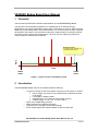
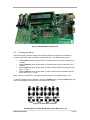
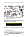
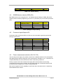
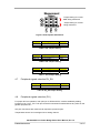
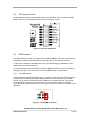
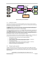
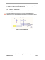
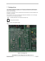
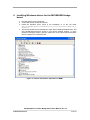
MC9S08QE8 Low Power Badge Board User Manual Document History Revision 1.0 1.1 Author H. Letourneau M. Leger Description Document creation Documentation Date Feb 11 2008 March 30, 2008 Table of Contents Document History ...........................................................................................................2 9S08QE8 Badge Board User Manual..................................................................................4 1 Foreword ...................................................................................................................4 2 Introduction ...............................................................................................................4 Running the demo ................................................................................................... 5 2.1 3 Kit Contents ...............................................................................................................6 4 Hardware Setup .........................................................................................................6 Configuration jumpers ............................................................................................. 6 4.1 OSBDM Control (OSBDM_cntrl) ............................................................................ 7 4.2 Capacitor leakage jumper (P1) ................................................................................ 7 4.3 OSBDM device selector (BDM_EN) ........................................................................ 8 4.4 Processor Inputs/Outputs P6................................................................................... 8 4.5 Power measurement selection (P8, P9, P10) ......................................................... 8 4.6 Peripheral signals selection RV_EN ........................................................................ 9 4.7 Peripheral signals selection (P11) ........................................................................... 9 4.8 5 Configuration ........................................................................................................... 10 Power source ......................................................................................................... 10 5.1 5.1.1 Battery operation ................................................................................................... 10 5.1.2 USB operation ....................................................................................................... 10 5.1.3 External Supply operation ..................................................................................... 10 5.1.4 S1 On/Off Switch ................................................................................................. 10 S2 Peripheral Power.............................................................................................. 11 5.2 BDM Interface ........................................................................................................ 11 5.3 5.3.1 Force BDM Mode................................................................................................... 11 6 Operation ................................................................................................................ 12 Current measurement circuit (refer to schematics) ............................................... 12 6.1 6.1.1 Taking a current measurement.............................................................................. 12 6.1.2 Measurement accuracy ......................................................................................... 12 6.1.3 Measurement selection.......................................................................................... 12 6.1.4 Calibration Procedure ............................................................................................ 13 External crystal operation ...................................................................................... 13 6.2 Capacitive Touch keypad ...................................................................................... 14 6.3 7 Prototype Area ......................................................................................................... 15 8 Installing Windows drivers for the MC9S08QE8 badge board. ....................................... 16 9 Programming (Application and Control Processor) ....................................................... 17 Application Processor programming ..................................................................... 17 9.1 Control processor programming ............................................................................ 17 9.2 Programming Procedure ....................................................................................... 17 9.3 OSBDM Programming (908JB16) ......................................................................... 20 9.4 MC9S08QE8 Low Power Badge Board User Manual, Rev 1.0 Future Electronics 2 of 20 Table of Figures Figure 1: Typical current consumption profile ........................................................................... 4 Figure 2: MC9S08QE8 Badge Board ....................................................................................... 5 Figure 3: Board Demo switches ............................................................................................... 5 Figure 4: Default Jumper Settings ............................................................................................. 7 Figure 5: Board power distribution............................................................................................. 9 Figure 6: S2 Power distribution ............................................................................................... 11 Figure 7: Force BDM connection............................................................................................. 11 Figure 8: Board power distribution........................................................................................... 13 Figure 9: Touch sensing Interface ........................................................................................... 14 Figure 10: Prototype area........................................................................................................ 15 Figure 11: Device detected as “Open Source BDM“ ............................................................... 16 Figure 12: Selecting OpenSourceBDM target ......................................................................... 18 Figure 13: Warning message, click ok to continue.................................................................. 19 Figure 14: Mass erase warning message, click ok to proceed ............................................... 19 Figure 15: ICP programming interface .................................................................................... 20 Index of Tables Table 1: OSBDM_cntrl Jumper Setting ..................................................................................... 7 Table 2: P1 Jumper Setting ....................................................................................................... 8 Table 3: BDM_EN Jumper Setting ............................................................................................ 8 Table 4: P6 Jumper Setting ....................................................................................................... 8 Table 5: P8 Jumper Setting ....................................................................................................... 9 Table 6: P9 Jumper Setting ....................................................................................................... 9 Table 7: P10 Jumper Setting ..................................................................................................... 9 Table 8: RV_EN Jumper Setting ............................................................................................... 9 Table 9: P11 Jumper Setting ................................................................................................... 10 Table 10: P7 Power source select........................................................................................... 10 MC9S08QE8 Low Power Badge Board User Manual, Rev 1.0 Future Electronics 3 of 20 9S08QE8 Badge Board User Manual 1 Foreword This document specifies the hardware implementation of the 9S08QE8 Badge Board. The purpose of this development platform is to facilitate (but is not restricted to) the development of low power applications where power consumption is an issue. While most lab DMM only provide steady state current measurement, our on board control circuitry computes the integral of the dynamic current levels in response to external stimuli or internal processor resources typical of power saving applications. The user may then efficiently optimize the code to lower the overall power consumed. Average current Power Long term energy average over user defined time period Time PRESS START PRESS START Figure 1: Typical current consumption profile 2 Introduction The MC9S08QE8 Badge board is an evaluation platform featuring: • • • • • Long term average current consumption monitoring circuit (100nA to 100mA) Able to supply monitored or unmonitored power to different sections of the board LCD display to display results Integration time up to 9999 seconds (almost 3 hours) Variable supply: 2.0 to 3.3 V at up to 100mA. Open Source BDM debug interface SMD Prototype Area (patterns with vias) Capacitive touch sensing (4 electrodes) keypad) Power related application software based on labs and exercises. MC9S08QE8 Low Power Badge Board User Manual, Rev 1.0 Future Electronics 4 of 20 Figure 2: MC9S08QE8 Badge Board 2.1 Running the demo The board’s main processor already has a demo application programmed. Essentially, it provides 4 discrete modes of operation controlled by the 4 on board switches SW1-4. • • • • Pressing SW1 will place the processor in full speed mode running at 10 MHz (avg = ~3.2mA) Pressing SW2 will place the processor in LPRUN mode running at 250 KHz (avg = ~280uA) Pressing SW3 will place the processor in STOP3 mode with RTC running with LPO (avg = ~4.5uA) Pressing SW4 will place the processor in STOP2 mode with RTC disabled (lowest power mode, avg = ~0.3uA) When a button is pressed, the corresponding LED will light up for approximately 1 sec. To start an average current calculation, press the START button. Pressing START again will stop the averaging process and hold the results on the screen. Figure 3: Board Demo switches MC9S08QE8 Low Power Badge Board User Manual, Rev 1.0 Future Electronics 5 of 20 3 Kit Contents Each kit is packaged with the following: - 9S08QE8 Badge Board - CodeWarrior for HC(S)08 6.1 CD ROM - CD including Labs, sample code and various documentation - USB cable A/B - Quick start guide Please note that the power supply and AA batteries are not included in this particular kit. The board can be powered using the included USB cable. 4 Hardware Setup This development board is equipped with 3 microcontrollers: • The MC9S08QE8 for code development. This is the device under test U1 located in the center of the board. • A second MC9S08QE8 is dedicated to monitor the power consumption of the device under test. • A MC908JB16 used for BDM debug interface When powering the board the 5V_OK LED should turn on and the LCD should indicate an integration time of 0s a current of 000.0uA and the main supply voltage which can be adjusted by R43 potentiometer. 4.1 Configuration jumpers Figure 4 shows the factory default jumper settings, representing the following configuration: - Board power from USB BDM in default operation CPU power measurement BDM connected to the Device Under Test LEDs and Switches connected to the I/Os External crystal connections MC9S08QE8 Low Power Badge Board User Manual, Rev 1.0 Future Electronics 6 of 20 Figure 4Error! No sequence specified.: Default Jumper Settings 4.2 OSBDM Control (OSBDM_cntrl) The OSBDM_cntrl jumper series (refer to Table 1) are used for normal operation or reprogramming the OSBDM controller. The reprogramming of the JB16 should only be done when absolutely necessary and one must use extreme precaution. The Freescale Forum should be consulted for information on OSBDM upgrades. Jumper Pin 1-2 Pin 3-4 Pin 5-6 Pin 7-8 Normal operation ON OFF OFF OFF Reprogramming OFF ON ON ON Default ON OFF OFF OFF Table 1: OSBDM_cntrl Jumper Setting The USB green led indicates the USB communication activity (See the LED section for more details). Please note that the entire BDM interface is powered through the 5V supply from the USB port. The whole board can be powered from USB as well as other sources. 4.3 Capacitor leakage jumper (P1) At very low power operation, very small current leakage from components such as electrolytic capacitors can become significant. Jumper P1 can used to connect an additional tantalum decoupling capacitor across the QE8 supply and see the effect on overall power consumption due to leakage. MC9S08QE8 Low Power Badge Board User Manual, Rev 1.0 Future Electronics 7 of 20 Jumper Pin 1-2 Additionnal Leakage ON No additional leakage OFF Default ON Table 2: P1 Jumper Setting 4.4 OSBDM device selector (BDM_EN) Both QE8 devices can be programmed. Two different jumper settings on BDM_EN can be used to perform firmware programming on the D.U.T. processor (U1) or the control processor (U6). Jumper Pin 1-2 Pin 3-4 Pin 5-6 Pin 7-8 Programming U1 (Application MCU) OFF OFF ON ON Programming U6 (Control MCU) ON ON OFF OFF Default OFF OFF ON ON Table 3: BDM_EN Jumper Setting 4.5 Processor Inputs/Outputs P6 Push button SW1 to SW4 and LED1 to LED4 can be connected the general purpose I/Os through connector P6. Jumper Pin 1-2 Pin 3-4 Pin 5-6 Pin 7-8 Pin 9-10 Pin 11-12 Pin 13-14 Pin 15-16 I/O pin PTA0 PTA1 PTA2 PTA3 PTC0 PTC1 PTC2 PTC3 Function SW1 SW2 SW3 SW4 LED1 LED2 LED3 LED4 Default ON ON ON ON ON ON ON ON Table 4: P6 Jumper Setting 4.6 Power measurement selection (P8, P9, P10) The on board power supply can provide current to the 3 different sections: CPU, Peripherals and SMD prototype area as being part of the measurement calculation or not. This allows for complete flexibility over which devices have their current being measured. Placing a jumper across the measurement supply will include whatever current being consumed in this area to be included in the calculation while the unmeasured selection still provide the same voltage but no current is being measured. Both power supplies have the capability to track each other so that there are no interfacing issues between each section. MC9S08QE8 Low Power Badge Board User Manual, Rev 1.0 Future Electronics 8 of 20 Jumper setting for current NOT being measured Jumper setting for current being measured Figure 5: Board power distribution Jumper Pin 1-2 Pin 2-3 CPU Supply Measured supply Direct supply Default ON OFF Table 5: P8 Jumper Setting Jumper Pin 1-2 Pin 2-3 Peripheral Supply Measured supply Direct supply Default OFF ON Table 6: P9 Jumper Setting Jumper Pin 1-2 Pin 2-3 Proto Supply Measured supply Direct supply Default OFF ON Table 7: P10 Jumper Setting 4.7 Peripheral signals selection RV_EN Jumper Pin 1-2 Pin 3-4 Enabled Signal (If ON) Potentiometer on KBIP0 Photo sensor on KBIP1 Default OFF OFF Table 8: RV_EN Jumper Setting 4.8 Peripheral signals selection (P11) For proper I2C bus operation, both pull ups on SDA and SCL must be enabled by adding jumpers on I2C_PULL_EN. Pull ups can be left connected if needed without any effect on the general purpose I/Os SCI port connections are made to their respective processor pins. Temperature sensor U24 is assigned an to analog channel. MC9S08QE8 Low Power Badge Board User Manual, Rev 1.0 Future Electronics 9 of 20 Jumper Pin 1-2 Pin 3-4 Pin 5-6 Pin 7-8 Pin 9-10 Pin 11-12 Pin 13-14 Pin 15-16 Signal (If ON) Pull up i2C SDA Pull up I2C SCL SCI port RTS SCI port CTS No connect Temp Sensor Output SCI port RX Data SCI port TX Data Default OFF OFF OFF OFF OFF OFF OFF OFF Table 9: P11 Jumper Setting 5 Configuration 5.1 Power source The Power Source Select header P7 is used to select the source used to power the board. Only one source should be selected at a time with a single jumper on P7. Jumper Pin 1-2 Pin 3-4 Pin 5-6 Power Source USB EXTERNAL CPU Default ON OFF OFF Table 10: P7 Power source select 5.1.1 Battery operation Two AA batteries can be used to power the board. This 3V source is increased to 5 V through a boost regulator circuit. To power cycle a board, simply turn the switch S1 to the off position for at least 4 to 5 seconds. 5.1.2 USB operation 5V USB power can be used to power the board. To power cycle a board powered from USB, the cable must be physically disconnected and reconnected. 5.1.3 External Supply operation An external power source can supply power to the board. Any voltages from 8 to 15V DC or 6 to 12 V AC is acceptable. A bridge rectifier is used to enable AC voltages and DC voltages with the center post of the connector at any polarity. 5.1.4 S1 On/Off Switch S1 controls the battery power. To power cycle the board when a source other than the batteries are used, disconnect the source, wait for a few seconds and reconnect. MC9S08QE8 Low Power Badge Board User Manual, Rev 1.0 Future Electronics 10 of 20 5.2 S2 Peripheral Power On board peripherals are powered separately through dip switch S2. This scheme enables better control over which peripherals are powered consuming current. Figure 6: S2 Power distribution 5.3 BDM Interface The BDM interface is based on the Open Source BDM (OSBDM). When the USB interface is enumerated in Windows and the BDM is functioning properly, the USB led will be on. A cable can be installed on the BDM connector to provide debugging capabilities to other boards and/or Freescale processors. An external BDM interface such as the P&E Micro USBMULTILINK can also be used as the debugging interface. In this case, the on boards OSBDM should not be powered. 5.3.1 Force BDM Mode During low power application development, it is possible to leave the application processor in a sleep state where all the peripherals, BDM included, are not functioning. To force BDM activity, the processor must wake up with the BDM pin connected to ground. This is easily accomplished by inserting a jumper between pins 1 and 2 (shown below) on the BDM connector when powering up the board. The jumper must then be removed to resume normal operation. Figure 7: Force BDM connection MC9S08QE8 Low Power Badge Board User Manual, Rev 1.0 Future Electronics 11 of 20 6 Operation 6.1 Current measurement circuit (refer to schematics) The power measurement circuit is composed of a current sense resistor (R34), a differential voltage to current converter (U15, R36-37 and Q1) and a low leakage film capacitor (C32). A current proportional to the voltage drop in the current sense resistor is sourced into C32 and generates a linear ramp. At low integrating ramp speed, the capacitor voltage is read by an A/D converter and ramp rate is converted to current information. At higher power, the integrating capacitor’s reset signal is used as a frequency generator to evaluate the current. The current readout is the average current over the time period indicated by the time counter on the LCD display. All the I/Os of the application processor were made to be freed from any default connections (with a few exceptions) as to not include any I/O leakage from peripherals in the power consumption calculation. 6.1.1 Taking a current measurement Pressing the START button will begin an average current measurement. The time count will reset and increase every second. The power reading will appear and may fluctuate at the beginning depending on how dynamic the application is. Very low current will require a longer average time to provide stable results. To stop the process, press START again. Also, please note that the debugger must be closed and the USB cable removed to make accurate low power measurements. If there is still communication with the application processor and the debugger, low power will not be achieved as these modules are still enabled inside the device. 6.1.2 Measurement accuracy As with any averaging process, the longer the average time the more precise the results will be. In a dynamic application where the current levels change rapidly, the instant when the user press the START button may differ from one test to the other therefore including or excluding current peaks from the average and providing different results. This is not related to the precision or accuracy of the measurement circuit itself which is usually within a few percent. Please note, changing the voltage setting during an average calculation will not provide correct results. 6.1.3 Measurement selection The MC9S08QE8 badge board has two power supplies, one is direct to the load and the second is monitored by the current measurement circuit. By selecting the proper jumper settings on P8, P9 and P10, one can measure the power consumption of the application processor, its peripherals and from the prototype area in any combination. Please refer to section 4.6 for more information on proper jumper settings. MC9S08QE8 Low Power Badge Board User Manual, Rev 1.0 Future Electronics 12 of 20 5V Regulator #1 2.0V to 3.3V USB Power Source Select Power In Manual adjust Measurement Select QE8 MPU DUT SMD Proto Area Regulator #2 Low Power Peripheral Boost circuit Power Measurement Circuit Battery Figure 8: Board power distribution 6.1.4 Calibration Procedure The current measurement circuit will require calibration every time the control processor is reflashed since configuration parameters stored in a portion of the flash (Sector 0xFC00) will be erased during the mass erase process. A calibration procedure may also be forced when powering the board while holding down the CALIBRATE button. This will ensure the board is operational with different environmental conditions like temperature or drift due to component aging. To properly calibrate the measurement circuit, jumpers P8, P9 and P10 are required to be in the UNMEASURED position (please refer to Table 5, 6 and 7). The calibration process outlined below requires the user to follow the steps in a specific manner. Failure to do so may provide slight offset and erroneous results. When the calibration is complete, the data will automatically be stored in flash and normal operation will resume. The procedure will calibrate various setpoints at different voltages and loads. The display will provide specific directives as to when to press buttons and change the voltage. • • • • • • • • 6.2 Place jumpers on P8, P9 and P10 to the unmeasured position Set voltage to maximum Press and hold the calibrate button until the release message (~4 seconds) Wait for calibration (up to 10 seconds depending on board) Set voltage to minimum Press and hold the calibrate button until the release message (~4 seconds) Wait for calibration (up to 10 seconds depending on board) Results will be written to flash automatically External crystal operation A 4MHz crystal was used as an external clock source. With the current QE8 clock divider settings, the lowest bus frequency configuration is 250 kHz. Even if this exceeds the device’s specification of 125 kHz in Low Power Run Mode (in FBE mode), the device can still operate without problems. MC9S08QE8 Low Power Badge Board User Manual, Rev 1.0 Future Electronics 13 of 20 If the user wishes to do 32 kHz low power mode tests, the crystal can be interchanged with a low cost 32.768 kHz watch crystal. Depending on the crystal specifications, capacitors C4, C5, resistor R4 and R6 should be removed or adjusted 6.3 Capacitive Touch keypad The board is equipped with a set of 4 touch pads to demonstrate Freescale’s Proximity Sensing Solutions Software. Care must be taken to make sure the pullup resistors are powered via S2 switch 7. Shared functions on P11 (IIC and serial interface) must be freed by removing any jumpers. Figure 9: Touch sensing Interface MC9S08QE8 Low Power Badge Board User Manual, Rev 1.0 Future Electronics 14 of 20 7 Prototype Area The onboard prototype area provides a convenient way to add simple user defined circuits such as analog (amplifiers, comparators, etc…) and logic functions and various discretes in surface mount technology. Each pad is connected to a via for connection with a fine jumper wire. Various footprints were included for convenience. Power supplied to this area can be either part of the power calculation or not. On the upper connector area, pins are denoted as follows: 2-3.3VDC (measured or not measured as set per P10) 0 VDC ground connections 5 VDC boost regulated supply Figure 10: Prototype area MC9S08QE8 Low Power Badge Board User Manual, Rev 1.0 Future Electronics 15 of 20 8 Installing Windows drivers for the MC9S08QE8 badge board. 1- Plug the device into any USB port 2- A new USB device should be detected 3- Install the Windows driver found in the installation or on the CD under QE8_CD\OSBDM\OpenSourceBDM\Release_Files\OpenSourceBDM_S08_W inDriver . 4- The device should now be detected as “Open Source BDM (LibUSB-Win32)” into the “LibUSB-Win32 Devices” section in your device manager window. To open the device manager window, open the system link in the control panel and select device manager in the hardware tab. Figure 11: Device detected as “Open Source BDM“ MC9S08QE8 Low Power Badge Board User Manual, Rev 1.0 Future Electronics 16 of 20 9 Programming (Application and Control Processor) 9.1 Application Processor programming Normal operation will have the jumpers on BDM_EN connector set to program the Application Processor (jumpers over “Target” portion). Please note that programming and I2C pullup resistors are powered from the measured supply so any pullup leakage, if enabled via the jumpers, will be accounted for in the measurement. If more accurate results are needed, jumpers on BDM_EN should be removed and internal pull-ups enabled as to not leave these inputs floating (pin PTA4/ACMP1O/BKGD/MS and PTA5/IRQ/TCLK/RESET). 9.2 Control processor programming Programming of the control processor may be needed for firmware upgrade. It is good practice (and highly recommended) to always run the latest firmware. Please consult the web link provided in the quick start guide to gain access to the latest information and upgrades. Setting the jumpers on BDM_EN to program the control processor requires the power supply be set to 3.3V. Jumpers must also be placed back to their original position, debugger closed and the board gone through a power up sequence before the new code is in effect. If the board is powered from USB, disconnecting and reconnecting the USB cable will suffice. Real time debugging of the control processor’s application will provide erroneous measurement results as the default TRIM value for the on chip oscillator is set to default at 128 therefore changing the time base for the calculations. 9.3 Programming Procedure 1234567- Select the proper device with the jumper setting indicated in Table 3. Launch CodeWarrior for HC08 V6.1 (CodeWarrior IDE) In the IDE’s initial startup menu click Start Using CodeWarrior Click File menu and then click Open… Find and select the project to open (*.mcp) and then click Open. Make sure that your MC9S08QE8 badge board is connected to your USB port. Select the HCS08 Open Source BDM target in CodeWarrior’s IDE and then click the Debug icon (Error! Reference source not found.). The design will then compile and the debugger will start. MC9S08QE8 Low Power Badge Board User Manual, Rev 1.0 Future Electronics 17 of 20 Figure 12: Selecting OpenSourceBDM target 8- Once the debugger is started, a warning window should pop-up telling that the current application execution will stop, click ok to continue (see Figure 12) MC9S08QE8 Low Power Badge Board User Manual, Rev 1.0 Future Electronics 18 of 20 Figure 13: Warning message, click ok to continue 9- Another warning message will appear telling that the EEPROM and FLASH will be both mass erased and the application will then be programmed, click ok to continue (see Figure 13). The EEPROM and FLASH is then erased and reprogrammed with the new application. Figure 14: Mass erase warning message, click ok to proceed 10- To execute the programmed application simply click Start/Continue in the Run menu of the debugger (or green arrow) or press F5. MC9S08QE8 Low Power Badge Board User Manual, Rev 1.0 Future Electronics 19 of 20 9.4 OSBDM Programming (908JB16) From time to time, it may be required to upgrade to a new version of the debug interface processor. Should this need arise, upgrading the BDM controller‘s firmware is done via USB with the help of a software utility called USBICP available on the install CD or the Freescale website under the 908JB16 8 bit processor section. To execute this, please refer to the OSBDM_cntrl jumper setting of table 1 and connect the USB cable in the connector. When starting the USBICP application, you will be prompted to select the device specific file which is located in the same directory as the USBICP program and is named “jb16icp_me.imp” and click OK. Once loaded, the interface will appear as shown below. After selecting the new firmware update file (should be S19 extension and format), click the Erase FLASH button then click the program. Once the flash process is completed, close the application, disconnect the USB and place the OSBDM_cntrl jumpers in their original positions. Figure 15: ICP programming interface MC9S08QE8 Low Power Badge Board User Manual, Rev 1.0 Future Electronics 20 of 20


![[DRAFT] DEMO908JL16 User`s Manual](http://vs1.manualzilla.com/store/data/005639706_1-2a84cd2ce2f0b318fdb7aae7896f2a79-150x150.png)
