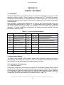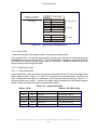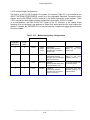
1
Rev: PR-071006
PCI66-16AO16FLV
16-BIT, 16-CHANNEL, HIGH-SPEED
PCI ANALOG OUTPUT BOARD
With Balanced Differential Outputs and Reconstruction Filters
_______________________
REFERENCE MANUAL
PRELIMINARY
________________________________________________________________________________________
General Standards Corporation Ph:(256)880-8787 FAX:(256)880-8788 Email: [email protected]
MAN-PCI66-16AO16FLV
PCI66-16AO16FLV
Copyright (C) 2006 General Standards Corp.
Additional copies of this manual or other General Standards Co. literature may be obtained from:
General Standards Corp.
8302A Whitesburg Dr.
Huntsville, Alabama 35802
Telephone: (256) 880-8787
FAX:
(256) 880-8788
The information in this document is subject to change without notice.
General Standards Corp. makes no warranty of any kind with regard to this material, including, but not limited to, the implied warranties of
merchantability and fitness for a particular purpose. Although extensive editing and reviews are performed before release to ECO control,
General Standards Corp. assumes no responsibility for any errors that may exist in this document. No commitment is made to update or keep
current the information contained in this document.
General Standards Corp. does not assume any liability arising out of the application or use of any product or circuit described herein, nor is any
license conveyed under any patent rights or any rights of others.
General Standards Corp. assumes no responsibility resulting from omissions or errors in this manual, or from the use of information contained
herein.
General Standards Corp. reserves the right to make any changes, without notice, to this product to improve reliability, performance, function, or
design.
All rights reserved.
No part of this document may be copied or reproduced in any form or by any means without prior written consent of General Standards Corp.
________________________________________________________________________________________
General Standards Corporation Ph:(256)880-8787 FAX:(256)880-8788 Email: [email protected]
PCI66-16AO16FLV
TABLE OF CONTENTS
SECTION
1.0
TITLE
INTRODUCTION
_
PAGE
1-1
1.1
General Description
1-1
1.2
Functional Overview
1-2
2.0
INSTALLATION AND MAINTENANCE
2-1
2.1
Board Configuration
2-1
2.2
Installation
2-1
2.2.1
Physical Installation
2-1
2.2.2
Input/Output Cable Connections
2-2
2.3
2.3.1
System Configuration
Output Considerations
2-3
2-3
2.3.1.1
Output Configurations
2-3
2.3.1.2
Line Losses
2-4
2.3.1.3
Remote Ground Sensing
2-4
External Clock and Trigger I/O
2-5
2.3.2
2.3.2.1
Sample Clock Output
2-5
2.3.2.2
Burst Trigger I/O
2-5
2.3.3
Multiboard Synchronization
2-5
2.3.3.1
Synchronized Bursts
2-5
2.3.3.2
Synchronized Clocks
2-5
2.4
Maintenance
2-6
2.5
Reference Verification
2-6
2.5.1
Equipment Required
2-7
2.5.2
Verification Procedure
2-7
3.0
CONTROL SOFTWARE
3-1
3.1
Introduction
3-1
3.2
Board Control Register
3-1
3.3
Configuration and Initialization
3-1
3.3.1
Board Configuration
3-1
3.3.2
Initialization
3-3
________________________________________________________________________________________
General Standards Corporation Ph:(256)880-8787 FAX:(256)880-8788 Email: [email protected]
i
PCI66-16AO16FLV
TABLE OF CONTENTS (Continued)
SECTION
3.4
3.4.1
3.4.1.1
TITLE
_
PAGE
Analog Output Control
3-4
Data Organization
3-5
Active Channels
3-5
3.4.1.1.1
Selection
3-5
3.4.1.1.2
Loading
3-5
3.4.1.2
Data Frame
3-6
3.4.1.3
Output Data Format
3-6
3.4.1.3.1
Output Data Buffer
3-6
3.4.1.3.2
Output Data Coding
3-7
Voltage Range Selection
3-7
3.4.1.4
3.4.2
Output Buffer
3-7
3.4.2.1
Buffer Operations Register
3-7
3.4.2.2
Active Buffer
3-9
3.4.2.3
Status Flags
3-9
3.4.2.4
Open Buffer
3-9
3.4.2.5
Circular Buffer
3-10
3.4.3
Output Clocking
3-11
3.4.3.1
Clock Source
3-11
3.4.3.1.1
External Clock
3-11
3.4.3.1.2
Internal Rate Generator
3-11
3.4.3.2
Simultaneous Clocking
3-12
3.4.3.3
Sequential Operation
3-12
3.4.4
Sampling Mode
3-12
3.4.4.1
Continuous Sampling
3-12
3.4.4.2
Data Bursts
3-13
3.4.5
Multiboard Synchronization
3-13
3.4.5.1
Synchronous Bursts
3-13
3.4.5.2
Synchronous Clocking
3-14
3.4.6
3.4.6.1
Function Generation
3-14
Periodic and One-Shot Functions
3-14
________________________________________________________________________________________
General Standards Corporation Ph:(256)880-8787 FAX:(256)880-8788 Email: [email protected]
ii
PCI66-16AO16FLV
TABLE OF CONTENTS (Continued)
SECTION
TITLE
_
PAGE
3.4.6.2
Multiple Functions
3-14
3.4.6.3
Functioning Sequencing
3-14
3.5
Autocalibration
3-16
3.6
Interrupt Control
3-16
3.6.1
Local Interrupt Request
3-16
3.6.2
Enabling the PCI Interrupt
3-17
3.7
Remote Ground Sensing
3-17
3.8
Application Examples
3-18
3.8.1
Sequential Direct Outputs
3-19
3.8.2
Simultaneous Direct (Single Group) Outputs
3-19
3.8.3
Continuous Function
3-20
3.8.4
Periodic Function
3-21
3.8.5
Function Burst
3-22
3.8.6
Function Sequencing
3-23
3.9
DMA Operation
3-24
3.10
Synchronization with Sigma-Delta Input Products
3-25
3.10.1
Adjustable Reference Frequency Control
3-25
3.10.2
Initiator/Target Configurations
3-26
3.11
Assembly Configuration Register
3-27
3.12
Output Filters
3-27
4.0
PRINCIPLES OF OPERATION
4-1
4.1
General Description
4-1
4.2
Analog Outputs
4-2
4.3
Autocalibration
4-2
4.4
Power Control
4-2
Appendix A
Local Register Quick Reference
A-1
Appendix B
Migration from the PC104P-16AO20
B-1
________________________________________________________________________________________
General Standards Corporation Ph:(256)880-8787 FAX:(256)880-8788 Email: [email protected]
iii
PCI66-16AO16FLV
LIST OF ILLUSTRATIONS
FIGURE
TITLE
_
PAGE
1.1-1
Physical Configuration
1-1
1.2-1
Functional Organization
1-2
2.2-1
Physical Installation
2-1
2.2-2
System I/O Connector
2-2
2.3-1
Output Configurations
2-3
2.3-2
Line Loss Versus Load Current
2-4
2.3-3
Multiboard Burst Synchronization
2-6
2.5-1
Reference Adjustment Access
2-7
3.4-1
Typical Buffer Loading Sequence
3-6
3.4-2
Open Buffer Data Flow
3-10
3.4-3
Circular Buffer Data Flow
3-10
3.4-4
Function Sequencing
3-15
4.1-1
Functional Block Diagram
4-1
________________________________________________________________________________________
General Standards Corporation Ph:(256)880-8787 FAX:(256)880-8788 Email: [email protected]
iv
PCI66-16AO16FLV
LIST OF TABLES
TABLE
TITLE
_
PAGE
2.2-1
System I/O Connector Pin Functions
2-2
2.5.1
Reference Verification Equipment
2-7
3.1-1
Control and Data Registers
3-1
3.2-1
Board Control Register
3-2
3.3-1
Configuration Operations
3-3
3.4-1
Summary of Output Control Parameters
3-4
3.4-2
Channel Selection Register
3-5
3.4-3
Output Data Buffer
3-6
3.4-4
Output Data Coding; D15..D00
3-7
3.4-5
Buffer Operations Register
3-8
3.4-6
Active Buffer Size
3-9
3.4-7
Sample Rate Control Register
3-11
3.4-8
Sample Rate Selection
3-12
3.6-1
Interrupt Event Selection
3-17
3.8-1
Summary of Operation Examples
3-18
3.8-2
Initial Operations
3-18
3.8-3
Sequential Direct Outputs Example
3-19
3.8-4
Simultaneous Direct Outputs Example
3-19
3.8-5
Continuous Function Example
3-20
3.8-6
Periodic Function Example
3-21
3.8-7
Function Burst Example
3-22
3.8-8
Function Sequencing Example
3-23
3.9-1
Typical DMA Register Configuration
3-24
3.10-1
Adjustable Reference Frequency Control Register
3-25
3.10-2
Multiboard Clocking Configurations
3-26
3.11-1
Assembly Configuration Register
3-27
________________________________________________________________________________________
General Standards Corporation Ph:(256)880-8787 FAX:(256)880-8788 Email: [email protected]
v
PCI66-16AO16FLV
(This page blank intentionally)
________________________________________________________________________________________
General Standards Corporation Ph:(256)880-8787 FAX:(256)880-8788 Email: [email protected]
vi
PCI66-16AO16FLV
SECTION 1.0
INTRODUCTION
1.1 General Description
The PCI66-16AO16FLV board provides precision high-speed analog output capability for PCI
applications. Sixteen 16-bit analog output channels provide either single-ended or balanced
differential output configurations, with two selectable high-order reconstruction filters in each
channel. Output ranges are selectable as either ±1.5V and ±2.5V with a high-current output
option, or as ±5V and ±10V with a high-level option. The outputs can be clocked either
simultaneously or sequentially at rates up to 450 KSPS (Kilosamples per second) per channel.
The board is functionally and mechanically compatible with the IEEE PCI local bus specification
Revision 2.3 for 32-Bit transfers with 33MHz or 66MHz PCI clocking.
Power requirements consist of +5 VDC from the PCI bus in accordance with the specification,
and operation over the specified temperature range is achieved with conventional cooling.
Specific details of physical characteristics and power requirements are contained in the PCI6616AO16FLV product specification. Figure 1.1-1 shows the general physical configuration of the
board, and the arrangement of major components.
I/O CONNECTOR
ANALOG SECTION
DIGITAL SECTION
POWER
SECTION
Representative illustration. Details may vary.
Figure 1.1-1. Physical Configuration
The board is designed for minimum off-line maintenance, and includes internal monitoring and
autocalibration features that eliminate the need for disconnecting or removing the module from
the system for calibration. All system input and output connections are made through a single
68-pin I/O connector. Analog outputs are initialized to zero-level (midrange).
________________________________________________________________________________________
General Standards Corporation Ph:(256)880-8787 FAX:(256)880-8788 Email: [email protected]
1-1
PCI66-16AO16FLV
1.2 Functional Overview
Principal capabilities of the PCI66-16AO16FLV board are summarized in the following list of
features.
Sixteen Precision High-Speed 3-Wire Balanced Differential Analog Output Channels
16-Bit Resolution; D/A Converter per Channel
Data Rates up to 450K Samples per Second per Channel; 7.2MSPS Aggregate Rate
Outputs Update Simultaneously or Sequentially; Software-Selectable
Output Ranges of ±10V and ±5V, or ±2.5V and ±1.25V
8th-Order Continuous-Time Output Reconstruction Filters
D32 Transfer Compatibility in both 33MHz and 66MHz clocking Environments
256K-Sample Analog Output FIFO Buffer Configurable as Either Circular or Open
Continuous and Triggered-Burst (One-Shot) Output Modes
Data Rate Controlled by Adjustable Internal Clock or by Externally Supplied Clock
Supports Multiboard Synchronization.
On-demand Internal Autocalibration of all Channels
Differential Sync I/O Available for Synchronizing GSC's Sigma-Delta ADC Boards
Active Buffer Size Adjustable from 8 Samples to 256K Samples.
Figure 1.2-1 outlines the internal functional organization of the board. Sixteen analog output
channels are controlled through an analog output buffer, and can be updated either
simultaneously or sequentially. The outputs can be factory-configured either as 3-wire balanced
differential channels or as 2-wire single-ended channels. Two reconstruction filters are provided
in each channel.
System
I/O Conn
Voltage
Reference
Vtest
Selftest
Networks
Output
Buffer
PCI
Conn
Local
Controller
PCI
Interface
Adapter
16-Bit
Output DAC's
(16)
Reconstruction
Filters
(2 per Channel)
Analog
Outputs
(16 HI/LO Pairs)
Remote
Sense
+5VDC
Power
Conversion
+Vdd
-Vss
±5v
Ext Clock
& Trigger
Figure 1.2-1. Functional Organization
The output clocking rate can be controlled by an internal rate generator, or by an external clock
source. Internal selftest networks permit all channels to be calibrated to a single internal
voltage reference. On-demand autocalibration adjusts offset and gain calibration DAC's in each
output channel to calibrate all channels to an internal precision reference voltage.
________________________________________________________________________________________
General Standards Corporation Ph:(256)880-8787 FAX:(256)880-8788 Email: [email protected]
1-2
PCI66-16AO16FLV
SECTION 2.0
INSTALLATION AND MAINTENANCE
2.1 Board Configuration
This product has no field-alterable configuration features, and is completely configured at
the factory.
2.2 Installation
2.2.1 Physical Installation
To minimize the opportunity for accidental damage before installation, the board should be
stored in the original protective shipping envelope. System power must be turned OFF
before proceeding with the installation.
CAUTION:
This product is susceptible to damage from electrostatic discharge (ESD).
Before removing the board from the conductive shipping envelope, ensure
that the work surface, the installer and the host system are adequately
discharged to ground.
Before removing the board from the protective shipping envelope, select an empty PCI slot
in the host computer and, if a blank panel bracket is located in the slot position, remove the
bracket. Then remove the board from the shipping envelope and position the board with
the panel bracket oriented toward the expansion panel opening. Align the board's PCI
edge-connector with the mating connector on the motherboard, and carefully press the
board into position. Verify that the PCI connector has mated completely, and that the panel
bracket is seated against the fastener bracket above the panel opening. To complete the
installation, secure the panel bracket and rear support bracket with appropriate fasteners.
Do not overtighten.
________________________________________________________________________________________
General Standards Corporation Ph:(256)880-8787 FAX:(256)880-8788 Email: [email protected]
2-1
PCI66-16AO16FLV
2.2.2 Input/Output Cable Connections
System cable signal pin assignments are listed in Table 2.2-1. The system input/output
connector is designed to mate with a 68-Pin dual-cable high-density 0.05-inch connector,
Amp type 749621-7 or equivalent. This insulation displacement (IDC) cable connector
accepts standard 0.050-inch ribbon cable, with the pin numbering convention shown in
Table 2.2-1 and in Figure 2.2-2. "Twist and flat" cable is recommended for long cables
(greater than five feet). Contact the factory if preassembled cables are required.
Table 2.2-1. System I/O Connector Pin Functions
FUNCTION
ROW-B
PIN
FUNCTION
1
OUTPUT 00 LO *
1
OUTPUT 09 LO *
2
OUTPUT 00 HI
2
OUTPUT 09 HI
3
OUTPUT RTN 00 ****
3
OUTPUT 10 LO *
4
OUTPUT RTN 01
4
OUTPUT 10 HI
5
OUTPUT 01 LO *
5
OUTPUT RTN 09
6
OUTPUT 01 HI
6
OUTPUT RTN 10
7
OUTPUT RTN 01
7
OUTPUT 11 LO *
8
OUTPUT RTN 02
8
OUTPUT 11 HI
9
OUTPUT 02 LO *
9
OUTPUT 12 LO *
10
OUTPUT 02 HI
10
OUTPUT 12 HI
11
OUTPUT RTN 02
11
OUTPUT RTN 11
12
OUTPUT RTN 03
12
OUTPUT RTN 12
13
OUTPUT 03 LO *
13
OUTPUT 13 LO *
14
OUTPUT 03 HI
14
OUTPUT 13 HI
15
OUTPUT RTN 03
15
OUTPUT 14 LO *
16
OUTPUT RTN 04
16
OUTPUT 14 HI
17
OUTPUT 04 LO *
17
OUTPUT RTN 13
18
OUTPUT 04 HI
18
OUTPUT RTN 14
19
OUTPUT RTN 04
19
OUTPUT 15 LO *
20
OUTPUT RTN 05
20
OUTPUT 15 HI
21
OUTPUT 05 LO *
21
OUTPUT RTN 15
22
OUTPUT 05 HI
22
REM GND SENSE
23
OUTPUT RTN 05
23
OUTPUT RTN 15
24
OUTPUT RTN 06
24
VTEST OUT
25
OUTPUT 06 LO *
25
VTEST RETURN
26
OUTPUT 06 HI
26
DIGITAL RETURN
27
OUTPUT RTN 06
27
TRIG IN HI **
28
OUTPUT RTN 07
28
TRIG IN LO **
29
OUTPUT 07 LO *
29
TRIG OUT HI **
30
OUTPUT 07 HI
30
TRIG OUT LO **
31
OUTPUT RTN 07
31
DAC CLK OUT HI **
32
OUTPUT RTN 08
32
DAC CLK OUT LO **
33
OUTPUT 08 LO *
33
CLOCK I/O HI ***
34
OUTPUT 08 HI
34
CLOCK I/O LO ***
Row B
Row-A
Pin 34
I/O
Conn
PWB
Pin 1
a. I/O Connector (panel pin-view)
Cable-B *
Cable Connector
ROW-A
PIN
Pin-1 Wire
* 34-Conductor Ribbon
Cable; 0.050-in Spacing
Cable-A *
Pin-1 Wire
Front
Panel
b. System Cable Connector
Figure 2. System I/O Connector
The differential analog output configuration is shown. For optional single-ended outputs, OUTPUT XX HI is an output, and
OUTPUT XX LO is not used.
* "No-connect" for the 2-Wire single-ended configuration.
** Software-selectable as LVDS differential pairs. In TTL mode, 'HI' pins are signal pins, and 'LO' inputs should be
connected to digital return.
*** Bidirectional synchronization signal.
**** All OUTPUT RTN XX pins are connected together internally
Channels available in 8-Channel and 12-Channel configurations:
8-Channel Board: Channels 00-07, 12-Channel board: Channels 00-11.
________________________________________________________________________________________
General Standards Corporation Ph:(256)880-8787 FAX:(256)880-8788 Email: [email protected]
2-2
PCI66-16AO16FLV
2.3 System Configuration
2.3.1 Output Considerations
2.3.1.1 Output Configurations
The sixteen analog output channels can be factory-configured either as 3-wire balanced
differential outputs or as 2-wire single-ended outputs.
Balanced differential outputs (Figure 2.3-1a) provide the highest immunity to system noise
and interference, and are recommended in all systems in which the loads will accept
differential inputs. Each of the HI and LO outputs carries one-half of the output signal, with
the two halves operating as complementary signals of equal amplitude and opposite
polarity.. Since radiated interference usually affects both output lines simultaneously, the
coupled interference appears as a common mode signal which will be attenuated in a
differential load.
Vline
HI
+1
Rline
Rload
Vout
Vdac
LO
-1
(Vdac =
0.5*Vout)
RTN
Output
Return
Vload
Vline
Rline
Rgnd
Ignd
Remote
Ground
a. Differential Output Driver
Vline
HI
+1
Rline
Vload
Vdac
Vout
(Vdac =
1.0*Vout)
LO
Rload
(Not used)
RTN
Output
Return
Ignd
Rgnd
Remote
Ground
b. Single-Ended Output Driver
Figure 2.3-1. Output Configurations
For applications requiring single-ended outputs (Figure 2.3-1b), the output signal from each
channel appears on the associated HI output pin, and is generated with reference to the
output return pin. In general, single-ended outputs should drive only loads that are isolated
from system ground. The best results are obtained when the loads also are isolated from
each other
________________________________________________________________________________________
General Standards Corporation Ph:(256)880-8787 FAX:(256)880-8788 Email: [email protected]
2-3
PCI66-16AO16FLV
2.3.1.2 Line Losses
The voltage drop in ribbon cable can be a significant source of error in 16-bit systems, even
with relatively short cables driving low-current loads. Figure 2.3-2 shows the effect of load
current on the voltage drop in copper wire of various sizes.
A 2.0 milliamp load for
example, will insert a voltage drop of approximately 130 microvolts per foot in conventional
#28 AWG ribbon cable; twice that if the return line also is considered. Several feet of
ribbon cable therefore can produce significant errors in a 16-bit system, in which 1 LSB
may represent only 76 microvolts (±2.5 Volt range). High impedance loads however,
generally will not produce significant DC line loss errors.
300
200
Microvolts
per Foot
(20 Deg-C)
100
0
1.0
2.0
ao12app3
Figure 2.3-2. Line Loss Versus Load Current
2.3.1.3 Remote Ground Sensing
In single-ended applications, if a significant potential difference is expected between the
ground connection at the load and the output return from the board, the use of remote
ground sensing should be considered. When remote ground sensing is enabled through
application software, the input signal at the REM GND SENSE pin in the I/O connector
adjusts the output voltages of single-ended channels to compensate for a ground potential
at the load.
To provide correction for the potential difference between the analog output return and the
remote system ground, the REM GND SENSE input must be connected to the remote
system ground, and remote sensing must be enabled by the control software. If remote
ground sensing is not implemented, the REM GND SENSE input should be connected to
OUTPUT RETURN.
The remote sensing input affects all analog output channels, and consequently can be a
significant source of noise if not adequately protected from external sources of interference.
NOTE: Remote ground sensing is disabled for differential output channels.
________________________________________________________________________________________
General Standards Corporation Ph:(256)880-8787 FAX:(256)880-8788 Email: [email protected]
2-4
PCI66-16AO16FLV
2.3.2 External Clock and Trigger I/O
External clock and trigger input and output signals are software-selectable as either singleended TTL-compatible, or as low-voltage differential signaling (LVDS)-compatible.
In LVDS mode, the HI and LO pins in each pair correspond to the standard "+" and "-"
LVDS signals, respectively. LVDS inputs are terminated internally with 100 Ohms.
In TTL mode, the clock and trigger signals use the corresponding "HI" I/O pins, and the
"LO" pins should be grounded to digital return. TTL inputs are pulled HIGH internally
through approximately 5K-Ohms
2.3.2.1 Sample Clock Output
The DAC CLOCK OUT signal generates a 100-150ns low-going pulse each time the analog
outputs are updated, and can be used to synchronize the analog output clocking of multiple
clock target boards to a single clock initiator.
2.3.2.2 Burst Trigger I/O
If burst triggering is enabled by the control software, an external TTL or LVDS signal can
initiate a data burst by applying a HIGH-to-LOW transition on the TRIGGER INP pin in the
I/O connector. In order for the trigger input to be acknowledged, the TRIGGER OUT signal
must be HIGH, and the TRIGGER INP signal must go low for a minimum interval of 70
nanoseconds.. TRIGGER OUT goes LOW at the beginning of a burst, and returns HIGH
when the burst is completed.
To use the TRIGGER OUT as the sync input to an SDI-series sigma-delta board, connect
the TRIGGER OUT HI and LO outputs to the SYNC LO and HI inputs, respectively, of the
SDI board.
2.3.3 Multiboard Synchronization
2.3.3.1 Synchronized Bursts
If multiple boards are to be burst-synchronized together, the TRIGGER OUT signal from a
single burst-initiator, is connected to the TRIGGER IN pin of the first board in a series of
burst targets (Figure 2.3-3). The TRIGGER OUT from each target is connected to the
TRIGGER IN of the next target board in the series, and the TRIGGER OUT of the last
target is left unconnected. When operating in this triggered-burst mode, each burst-target
will initiate a single burst from its buffer each time the burst-initiator initiates a burst. The
initiator can be configured for either continuous or burst operation.
2.3.3.2 Synchronized Clocks
To clock-synchronize multiple boards together, the DAC CLOCK OUT from a clock initiator
is connected directly to the CLOCK IO pin of the first target board in a series of clock
targets. The DAC-CLOCK OUT from each target is connected to the CLOCK IO pin of the
next target in the series, and the CLOCK-IO pin of the last target is left unconnected. This
mode is configured by the application software as shown in Table 3.10-2.
________________________________________________________________________________________
General Standards Corporation Ph:(256)880-8787 FAX:(256)880-8788 Email: [email protected]
2-5
PCI66-16AO16FLV
TRIGGER Input
Burst
Initiator
Board
(No-Connect,
or
Burst-Trigger)
TRIGGER Output
TRIGGER Input
First
Burst Target
Board
TRIGGER Output
TRIGGER Input
Last
Burst Target
Board
TRIGGER Output
(No-Connect)
Figure 2.3-3. Multiboard Burst Synchronization
A clock target can be clocked by a HI-to-LO transition from any external TTL or LVDS
signal source connected to the CLOCK IO input. The input signal is edge-detected, and
must be low for a minimum interval of 70 nanoseconds in order to be recognized as a valid
clock.
2.4 Maintenance
This product requires no scheduled hardware maintenance other than periodic reference
verification. The optimum verification interval will vary, depending upon the specific
application, but in most instances an interval of one year should be sufficient. In the event
of a suspected malfunction, all associated system parameters, such as power voltages,
control bus integrity, and input signal levels, should be evaluated before troubleshooting of
the board itself is attempted. A board that is suspected to be defective should be returned
to the factory for problem analysis and repair.
2.5 Reference Verification
All output channels are software-calibrated to an internal voltage reference (Vtest) by an
embedded autocalibration firmware utility. The verification procedure presented here
describes the adjustment of the reference. For applications in which the system must not
be powered down, the board can be calibrated under normal operating conditions while
installed on the existing host board.
To eliminate the requirement for a special test connector, the two test points required for
calibration, VTEST OUT and VTEST RETURN, can be made available at a system
breakout connector or test panel. This arrangement also eliminates the necessity of
disconnecting the system input/output cable for reference verification or adjustment.
________________________________________________________________________________________
General Standards Corporation Ph:(256)880-8787 FAX:(256)880-8788 Email: [email protected]
2-6
PCI66-16AO16FLV
2.5.1 Equipment Required
Table 2.5-1 lists the minimum equipment requirements for verifying and adjusting the
internal voltage reference. Alternative equivalent equipment may be used.
Table 2.5-1. Reference Verification Equipment
EQUIPMENT DESCRIPTION
Digital Multimeter, 5-1/2 digit, 0.005%
accuracy for DC voltage measurements at
±10 Volts.
PCI expansion slot 33MHz or 66MHz;
32-Bit.
Standard 68-Pin, 0.05", dual-ribbon cable
connector, with test leads. (Not required if
calibration
test
points
are
made
permanently available at a system
connection point)
MANUFACTURER
MODEL
Hewlett Packard
34401A
(Existing host)
---
Amp
#1-746288-0
2.5.2 Verification Procedure
The following procedure describes the single adjustment that is necessary to ensure
conformance to the product specification.
Adjustment of the internal reference (Vtest) is performed with a single adjustment trimmer
that is accessed as shown in Figure 2.5-1. The adjustment seal on the trimmer should be
removed before beginning the procedure, and the trimmer should be resealed with a
suitable sealing agent after the adjustment has been completed. Thread-locking agents
should not be used.
REFERENCE ADJUSTMENT ACCESS
P2
B01
Figure 2.5-1. Reference Adjustment Access
________________________________________________________________________________________
General Standards Corporation Ph:(256)880-8787 FAX:(256)880-8788 Email: [email protected]
2-7
PCI66-16AO16FLV
This procedure assumes that the board to be verified is installed on a host board, and that
the host is installed in an operating system. The board can be operating in any mode when
the adjustment is performed.
1. Connect the digital multimeter between the VTEST OUT (+) and
VTEST RETURN (-) pins in the system I/O connector. Refer to Table 2.2-1 for pin
assignments.
2. If power has been removed from the board, apply power now and wait at least 15
minutes before proceeding.
3. The digital multimeter indication should indicate +9.9900 ±0.0010 VDC for the
High-Level range option, or +2.4975 ±0.0010 VDC for the High-Current option. If
the indication is not within this range, adjust the reference trimmer until an in-range
indication is obtained..
4. Reference verification or adjustment is completed. Remove all test connections.
________________________________________________________________________________________
General Standards Corporation Ph:(256)880-8787 FAX:(256)880-8788 Email: [email protected]
2-8
PCI66-16AO16FLV
SECTION 3.0
CONTROL SOFTWARE
3.1 Introduction
The PCI66-16AO16FLV is compatible with the PCI Local Bus specification revision 2.3 for D32
transfers at 33MHz or 66MHz. The PCI interface is controlled by a PLXTM PCI-9056 PCI adapter.
Configuration-space registers are initialized internally to support the location of the board on any
8-longword boundary in memory space. DMA access is supported for data transfers to the analog
output data buffer.
After initialization, communication between the PCI bus and the board takes place through the
control and data registers shown in Table 3.1-1. All data transfers are long-word D32. Reserved
bits in each register are ignored during write operations, and are forced LOW during read
operations. To ensure compatibility of applications with subsequent product upgrades, reserved
bits should be written as LOW.
Table 3.1-1. Control and Data Registers
OFFSET
REGISTER
MODE*
DEFAULT
PRIMARY FUNCTION
00
BOARD CONTROL (BCR)
R/W
0000_0810h
Board Control Register (BCR)
04
CHANNEL SELECTION
R/W
0000_FFFFh
Channel-enabling mask
08
SAMPLE RATE
R/W
0000_0096h
Analog output clocking rate selection
0C
BUFFER OPERATIONS
R/W
0000_340Fh
Buffer size selection and status flags
10
Firmware and Options **
RO
00XX_XXXXh
Firmware revision and hardware options
14
Autocal Values **
R/W
0000_0XXXh
---
18
OUTPUT DATA BUFFER
WO
0000_0000h
Analog output FIFO buffer
1C
ADJUSTABLE CLOCK
R/W
0000_0000h
Control of the adjustable clock generator.
* R/W = Read/Write; RO = Read-only; WO = Write-only .
** Maintenance register; shown for reference.
3.2 Board Control Register
The Board Control Register (BCR) controls primary board functions, including burst control,
autocalibration, and interrupt event selection. Table 3.2-1 provides a brief description of each bit
field in the BCR, as well as indicating an associated section in the text.
3.3 Configuration and Initialization
3.3.1 Board Configuration
During board configuration, initial values for both the PCI configuration registers and the internal
control logic are extracted from internal nonvolatile read-only memory. This process is initiated by
a PCI bus reset, and should be required only once after the initial application of power. While the
PCI configuration registers are being loaded, the response to PCI target accesses is RETRY's.
Configuration operations are executed in the sequence shown in Table 3.3-1.
________________________________________________________________________________________
General Standards Corporation Ph:(256)880-8787 FAX:(256)880-8788 Email: [email protected]
3-1
PCI66-16AO16FLV
Table 3.2-1. Board Control Register
Offset: 0000h
BIT
MODE
D00
R/W
Default: 0000_ 0810h
DESIGNATION
BURST ENABLED
DEF
DESCRIPTION
REF
0
Selects burst-mode if HIGH, continuous-mode if
LOW.
3.4.4,
3.4.5
D01
RO
BURST READY
0
If HIGH, indicates that a burst trigger will be
accepted. If LOW, indicates that a burst is in
progress, and that a trigger will not be accepted.
Available as an interrupt condition.
D02
R/W
*BURST TRIGGER
0
Software burst trigger, asserted HIGH.
only when BURST ENABLED is asserted.
D03
R/W
REMOTE GROUND SENSE
0
Correction is made for remote ground potentials
when this bit is HIGH.
3.7
D04
R/W
OFFSET BINARY
1
Selects offset-binary data format when asserted
HIGH, or two's complement when LOW.
3.4.1.3
D05
R/W
DIFFERENTIAL SYNC I/O
0
Selects differential (LVDS) external clock/trigger
I/O when high, or TTL clock/trigger I/O when low.
3.4.5
D06
R/W
DISABLE EXT BURST TRIG
0
Disables external burst trigger input.
3.4.4.2
D07
R/W
SIMULTANEOUS OUTPUTS
0
When HIGH, selects simultaneous output
clocking. When LOW, selects sequential clocking.
Default is LOW; i.e.: sequential.
3.4.3.2,
Active
3.4.3.3
D08-D10
R/W
INTERRUPT A0-A2
0
Interrupt event selection.
3.6
D11
R/W
INTERRUPT REQUEST FLAG
1
Set HIGH when the board asserts an interrupt
request. Clears the request when cleared LOW
by the bus.
D12
R/W
(Reserved)
0
---
---
D13
R/W
* AUTOCALIBRATION
0
Initiates autocalibration. Completion is available
as an interrupt condition.
3.5
D14
RO
AUTOCAL STATUS FLAG
0
Records the status of autocalibration;
pass, HIGH for fail.
D15
R/W
*INITIALIZE
0
LOW for
Initializes the board when set HIGH.
3.3.2
Sets all defaults for all registers.
D16
R/W
OUTPUT RANGE
0
Selects the output voltage range as:
3.4.1.4
High-Level Outputs:
0 => ±5V,
1 => ±10V,
High-Current Outputs:
0 => ±1.5V, 1 => ±2.5V.
D17
R/W
(Reserved)
0
D18-D19
R/W
OUTPUT FILTER
0
---
---
Selects the output filter for all channels:
0 =>
1 =>
2 =>
3 =>
D20-D31
---
(Reserved)
0
* Cleared automatically when operation is completed.
Inactive. Returns all-zero.
R/W = Read/Write;
--RO=Read-Only.
________________________________________________________________________________________
General Standards Corporation Ph:(256)880-8787 FAX:(256)880-8788 Email: [email protected]
3-2
3-12
Direct outputs; No filter,
Direct outputs; No filter,
Filter-A,
Filter-B.
PCI66-16AO16FLV
Board configuration terminates with the PCI interrupts disabled. Attempts to access the local bus
during configuration should be avoided until the PCI interrupts are enabled and an initializationcomplete interrupt request is asserted.
Table 3.3-1. Configuration Operations
Operation
Maximum Duration
PCI configuration registers are loaded from internal ROM
Internal control logic is configured from internal ROM
Internal control logic is initialized
3 ms
300 ms
3 ms
Loading of the PCI configuration registers is completed within 3 milliseconds or less after the
assertion of a PCI bus reset, and should be required only once after the initial application of power.
PCI register configuration terminates with the PCI interrupts disabled (Paragraph 3.6).
3.3.2 Initialization
Internal control logic can be initialized without invoking configuration by setting the INITIALIZE
control bit in the BCR. This action causes the internal logic to be initialized, but does not affect the
PCI configuration registers and does not reconfigure the internal control logic. Initialization
requires 3 milliseconds or less for completion, and produces the following default conditions:
•
•
•
•
•
•
•
•
•
•
•
•
•
•
•
The BCR is initialized; all defaults are invoked (Paragraph 3.2),
All analog outputs are set to zero-level (3.4.1.1),
All channels are active (3.4.1.1.1),
Data coding format is offset binary (3.4.1.3.2),
The low output range (±1.5V or ±5V) is selected (3.4.1.4),
The analog output buffer is reset to empty (3.4.2),
Buffer configuration is open (3.4.2.4), with maximum size selected (3.4.2.2),
Internal clocking is selected (3.4.3.1), and clocking is disabled (3.4.3),
The clocking rate generator is adjusted to 152.880KSPS (3.4.3.1.2),
Clocking mode is sequential (3.4.3.3) and continuous (3.4.4.1),
TTL sync I/O logic is selected (3.4.5),
The local interrupt request is asserted (ignored unless PCI interrupts are enabled) (3.6),
Remote ground sensing is disabled (3.7).
The adjustable clock rate generator is disabled (3.10),
Direct outputs are selected, and the output filters are disabled (3.12).
Upon completion of initialization, the INITIALIZE control bit in the BCR is cleared automatically.
________________________________________________________________________________________
General Standards Corporation Ph:(256)880-8787 FAX:(256)880-8788 Email: [email protected]
3-3
PCI66-16AO16FLV
3.4 Analog Output Control
This section describes those operations that control the movement of data from the PCI bus
through the analog output buffer. These functions include the selection of active channels, the
organization of data within the buffer, and the clocking of data from the buffer to the analog
outputs. The principal parameters associated with controlling the analog output channels are
summarized below in Table 3.4-1.
Section 3.8 provides detailed examples of analog output
operations.
Table 3.4-1. Summary of Output Control Parameters
Parameter
Data Control
Mode
Active Channels;
Channel Group
Active Buffer
Buffer
Configuration
Clock Source
Clocking Mode
Sampling Mode
Description
A single set of all active output channels constitutes an Active
Channel Group. Active channels are selected under a channel
mask.
Data Frame
All data values in the buffer comprise a Data Frame.
Data Coding
Output data can be coded either in offset-binary format or in two's
complement format.
Size Selection
The active buffer is a subset of the physical output data buffer.
Active buffer size is determined by the SIZE[3..0] control-bit field in
the buffer operations register.
Status Flags
Status flags buffer-empty, buffer-low-quarter, buffer-high-quarter
and buffer-full are provided for the active buffer.
Open
Data read from the buffer is used and then discarded, until the
buffer is empty.
Circular (closed)
Data within the buffer is recirculated. Each value read from the
output of the buffer FIFO is written back to the input of the FIFO.
An end-of-frame (EOF) flag tracks the movement of data through
the buffer.
External
External hardware provides the sample clock.
Internal
The sample clock is provided by an internal rate generator, at a
rate determined by the sample rate control register.
Simultaneous
At each clock occurrence, the next channel group (i.e.: a single
group of all active channel values) in the output buffer is transferred
to the respective analog output channels. All outputs are updated
simultaneously.
Sequential
At each clock occurrence, the next active channel value in the
output buffer is transferred to the associated analog output
channel, which is updated immediately.
Continuous
The contents of the output buffer are sampled continuously at the
selected clock rate.
Triggered Burst
A single data frame in the buffer is clocked to the outputs.
________________________________________________________________________________________
General Standards Corporation Ph:(256)880-8787 FAX:(256)880-8788 Email: [email protected]
3-4
PCI66-16AO16FLV
3.4.1 Data Organization
3.4.1.1 Active Channels
Analog output data is loaded into the output buffer in discrete groups, or frames, of channel data.
An active channel group consists of a single set of output values for all active channels.
Only active output channels receive data from the output buffer. A channel that is deselected to
the inactive state retains the last value that was received while the channel was still active. During
initialization, all channels are selected as active and are set to midrange (zero output level).
3.4.1.1.1 Selection
An output channel is selected as active by setting the corresponding ENABLE CHANNEL XX
selection bit HIGH in the Channel Selection Register, as shown in Table 3.4-2. A channel is
deselected to the inactive state by clearing the corresponding selection bit. To select Channels 3,
9 and 14 as active for example, the Channel Selection register would have the value 0000_4208h.
Channels 00-07 are available with 8-Channel boards, and Channels 00-11 are available with
12-Channel boards.
Table 3.4-2. Channel Selection Register
Offset: 0004h
Default: 0000_FFFFh
BIT
MODE
DESIGNATION
DESCRIPTION
D00
R/W
ENABLE CHANNEL 00
Channel-Enable mask. A channel is enabled if the
D01
R/W
ENABLE CHANNEL 01
associated mask bit is HIGH, or is disabled if the bit is LOW.
D02
R/W
ENABLE CHANNEL 02
D03
R/W
ENABLE CHANNEL 03
D04D15
R/W
ENABLE CHANNEL 04-15
D16D32
RO
(Reserved)
Inactive. Returns all-zero.
3.4.1.1.2 Loading
Channel data values are loaded into the output buffer in ascending order of the active channels.
The channel groups are loaded contiguously, beginning with the first group to be transferred to the
outputs, and proceeding sequentially to the last group. Figure 3.4-1 illustrates a loading example
that represents three active channels, with 100 values per channel. Each channel group consists
of active channels 3, 6 and 8, and consequently the value in the channel selection register is
0000_0148h.
________________________________________________________________________________________
General Standards Corporation Ph:(256)880-8787 FAX:(256)880-8788 Email: [email protected]
3-5
PCI66-16AO16FLV
Channels 3, 6 and 8 Enabled;
100 Values per Channel
LOADING
SEQUENCE
Channel Selection Register
= 0000_0148h
VALUE LOADED
0 (First)
Chan-3, 1st value
1
Chan-6, 1st value
2
Chan-8, 1st value
3
Chan-3, 2nd value
4
Chan-6, 2nd value
5
Chan-8, 2nd value
1st Channel Group
2nd Group
(Intermediate Values)
297
Chan-3, Last value
298
Chan-6, Last value
299
Chan-8, Last value
Last Group
Figure 3.4-1. Typical Buffer Loading Sequence
3.4.1.2 Data Frame
A data frame consists of an integral number of contiguous channel groups.
For triggered bursts, or for function concatenation, the last active channel in the last channel group
is designated as the end-of-frame (EOF). The EOF designation is applied by setting the EOF flag
(D16) HIGH when loading the last channel value into the buffer. Thereafter, the EOF flag follows
the last channel value through the buffer.
3.4.1.3 Output Data Format
3.4.1.3.1 Output Data Buffer
Analog output data values are written in word-serial sequence from the PCI bus to the Output Data
Buffer register shown in Table 3.4-3. Bits D15..0 represent the output data value. Bit D16 is set
HIGH to indicate the last value in a data frame, and is the end-of-frame (EOF) flag. Bits D31..17
are inactive and have no effect. Access to the output buffer is supported for both single-longword
transfers and single-address multiple-longword DMA transfers.
Table 3.4-3. Output Data Buffer
Default: N/A (Write-Only)
Offset: 0018h
BIT
MODE*
D00
WO
DESIGNATION
DATA 00
DESCRIPTION
Least significant data bit
D01-D14
WO
DATA 01 - DATA 14
Intermediate data bits
D15
WO
DATA 15
Most significant data bit
D16
WO
EOF FLAG
End-of-frame (EOF) flag.
D17-D31
WO
---
(Inactive)
* WO indicates write-only access. Read-access returns all-zero value.
________________________________________________________________________________________
General Standards Corporation Ph:(256)880-8787 FAX:(256)880-8788 Email: [email protected]
3-6
PCI66-16AO16FLV
3.4.1.3.2 Output Data Coding
Analog output data can be coded either in 16-bit offset binary format (Table 3.4-4) by asserting the
OFFSET BINARY control bit HIGH in the BCR, or in two's complement format by clearing the
control bit LOW. Analog output data transactions are D32 (32 bits), but the data significance is 16
bits.
Table 3.4-4. Output Data Coding; D15..D00
ANALOG OUTPUT LEVEL
DIGITAL
OFFSET BINARY
VALUE (Hex)
TWO'S COMPLEMENT
Positive Full Scale minus 1 LSB
XXXX FFFF
XXXX 7FFF
Zero plus 1 LSB
XXXX 8001
XXXX 0001
Zero
XXXX 8000
XXXX 0000
Zero minus 1 LSB
XXXX 7FFF
XXXX FFFF
Negative Full Scale plus 1 LSB
XXXX 0001
XXXX 8001
Negative Full Scale
XXXX 0000
XXXX 8000
Positive Full Scale is a positive level that equals the range option defined for the board (e.g.:
+5.000 Volts for the ±5V option). Negative Full Scale is the negative equivalent of positive fullscale. Full-scale Range (FSR) is the total voltage range for the output channel . One LSB equals
the full-scale range divided by 65,536. (e.g.: 152.59 microvolts for the ±5V option).
3.4.1.4 Voltage Range Selection
The OUTPUT RANGE control bit in the BCR selects the output range for all channels as ±10V or
±5V for the High-Level range option, or as ±2.5V or ±1.5V for the High-Current option. To minimize
potential stresses on sensitive load networks, the board initializes to the lowest available range.
For maximum accuracy, autocalibration should always be performed after a new output range is
selected.
3.4.2 Output Buffer
The physical output buffer consists of a 17-bit wide FIFO that has a capacity of 256K output
values. Each output value is 16 bits wide and occupies a single location within the FIFO. The 17th
bit is an end-of-frame flag that is attached to the last value in a data frame (Table 3.4-3). Data
values are transferred from the PCI bus to the analog output channels through an active buffer,
which is a subset of the physical buffer.
3.4.2.1 Buffer Operations Register
The buffer operations register (BOR) controls the configuration of the output buffer, as well as
related functions such as clocking and loading.
________________________________________________________________________________________
General Standards Corporation Ph:(256)880-8787 FAX:(256)880-8788 Email: [email protected]
3-7
PCI66-16AO16FLV
Table 3.4-5. Buffer Operations Register
Offset: 000Ch
Default: 0000_340Fh
BIT
MODE
DESIGNATION
DEF
D00-D03
R/W
SIZE 00-SIZE 03
D04
R/W
EXTERNAL CLOCK
0
Selects hardware or software clock source when HIGH, or
the internal rate generator when LOW. Default is LOW
(internal rate generator).
D05
R/W
ENABLE CLOCK
0
Enables output clocking when HIGH. Disables clocking when
LOW. Default is LOW (clocking disabled).
D06
RO
CLOCK READY
0
If external clocking is selected, indicates when HIGH that a
hardware or software clock will be accepted. If LOW,
indicates that the output is not ready to accept a clock.
Active only when external clocking is selected.
D07
R/W
*SW CLOCK
0
If external clocking is selected, produces a single output
clock event when asserted. Clears LOW automatically when
the clock event is completed. Active only when external
clocking is selected.
D08
R/W
CIRCULAR BUFFER
0
Selects circular buffer configuration if HIGH, or open selfflushing buffer configuration if LOW. Access for loading new
data into the circular buffer must be requested by asserting
LOAD REQUEST. Default is LOW; i.e. open buffer.
D09
R/W
*LOAD REQUEST
0
When set HIGH, requests loading access to the circular
buffer. Initializes LOW.
D10
RO
LOAD READY
1
Set HIGH when the frame index passes through zero, if both
CIRCULAR BUFFER and LOAD REQUEST are HIGH.
When HIGH, indicates that the circular buffer is ready to
accept new data.
Available as an interrupt condition.
Defaults HIGH.
D11
R/W
*CLEAR BUFFER
0
Resets the buffer to empty.
D12
R/W
BUFFER EMPTY
1
Status flags for the active buffer. Empty, lo-quarter and
D13
RO
BUFFER LOW
QUARTER
1
hi-quarter flags are available as interrupt events.
D14
RO
BUFFER HIGH
QUARTER
0
D15
RO
BUFFER FULL
0
D16
R/W
BUFFER OVERFLOW
0
Set HIGH when data is written to a full buffer. **
D17
R/W
FRAME OVERFLOW
0
Set HIGH when data is written to a closed buffer. **
D18-D31
RO
(Reserved)
0
Inactive. Returns all-zero.
Fh
DESCRIPTION
Size-selection bit field for the active buffer.
Defaults to 256K Samples.
* Clears LOW automatically when operation is completed.
** Remains HIGH until cleared by a direct write as LOW, or by initialization.
________________________________________________________________________________________
General Standards Corporation Ph:(256)880-8787 FAX:(256)880-8788 Email: [email protected]
3-8
PCI66-16AO16FLV
3.4.2.2 Active Buffer
The active buffer is a virtual buffer that represents a subset of the physical buffer, and which is the
working buffer through which all output data flows. The size of the active buffer is adjustable from
eight values up to the full size of the physical buffer. The buffer can be cleared to the empty state
by setting the CLEAR BUFFER control bit HIGH in the buffer operations register. CLEAR BUFFER
clears automatically after the reset operation has been completed.
NOTE: Data loss may occur if the buffer is allowed to fill completely.
The active buffer performs exactly like a physical buffer of the same size. That is, a full buffer will
accept no further data from the bus, and an empty buffer indicates that all outputs are idle. Buffer
status flags (empty, low-quarter, high-quarter and full) respond to the size of the active buffer, not
to the size of the physical buffer.
Active buffer size is determined by the SIZE[3..0] control bit field in the buffer operations register.
Available active buffer sizes are listed in Table 3.4-6.
Table 3.4-6. Active Buffer Size
SIZE[3:0]
BUFFER SIZE
(Total Channel Values)
SIZE[3:0]
BUFFER SIZE
(Total Channel Values)
0
8
8
2048
1
16
9
4096
2
32
A
8192
3
64
B
16384
4
128
C
32768
5
256
D
65536
6
512
E
131072
7
1024
F
262144
3.4.2.3 Status Flags
Status flags for the buffer operate with respect to the active buffer, and can initiate an interrupt
request if the active buffer becomes empty, 3/4-full, or less than 1/4-full. These flags are located in
the buffer operations register (Table 3.4-5), and are available as interrupt events (Table 3.6-1).
The BUFFER OVERFLOW flag is set HIGH if data is written to a full buffer, and the
FRAME OVERFLOW flag indicates that an attempt was made to write data to a closed buffer, each
indicating data loss. Once set, each of these flags remains HIGH until written LOW directly from
the bus, or by initialization .
3.4.2.4 Open Buffer
Data in an open buffer is discarded as it is used. Consequently, the buffer is self-flushing, and will
empty itself unless it is replenished from the bus. This mode of operation permits the continuous
flow of data from the PCI bus to the analog outputs. The buffer status flags are useful in this
situation, and provide an indication of whether the buffer is empty, less than 1/4 full (low-quarter),
greater than 3/4 full (high-quarter), or full. A full buffer will discard additional data from the bus,
while an empty buffer indicates that the outputs are idle. The low-quarter and high-quarter flags
are used to control data flow through the buffer when generating continuous functions.
________________________________________________________________________________________
General Standards Corporation Ph:(256)880-8787 FAX:(256)880-8788 Email: [email protected]
3-9
PCI66-16AO16FLV
The open-buffer configuration also can be used to produce a one-shot waveform, provided the
particular waveform is to be used only once. Figure 3.4-2 illustrates the movement of a single data
frame through an open buffer.
3.4.2.5 Circular Buffer
Data in a circular (closed) buffer is retained indefinitely. This configuration generally is
implemented to produce either periodic waveforms of constant frequency, or one-shot transient
waveforms that will be used repeatedly but not necessarily periodically. While closed, the buffer is
not accessible from the bus.
In Figure 3.4-3, a single data frame is loaded into the buffer. The buffer is then closed (CIRCULAR
BUFFER set HIGH) and clocking is enabled. The data frame subsequently circulates in the buffer
while passing data values to the output channels.
Active Buffer
From Bus
a. Buffer Loading
Input
Output
b. Frame Loaded
c. Clock Enabled;
Buffer Emptying
To DAC’s
Figure 3.4-2. Open Buffer Data Flow
An end-of-frame (EOF) flag accompanies the end-point, or last value in a data frame. The EOF
flag is D16 in the buffer, and is set HIGH when the last value in a data frame is loaded. This flag is
used during a triggered burst to define the last value in the burst. Multiple contiguous burst
functions can reside in the buffer simultaneously.
Active Buffer
EOF Flag
a. Frame Loaded
Circulating Data
b. Clock enabled;
Data Recirculating
To DAC’s
Figure 3.4-3. Circular Buffer Data Flow
________________________________________________________________________________________
General Standards Corporation Ph:(256)880-8787 FAX:(256)880-8788 Email: [email protected]
3-10
PCI66-16AO16FLV
3.4.3 Output Clocking
When the ENABLE CLOCK control bit in the buffer operations register is asserted HIGH, clocking
is enabled and the active analog outputs are updated at each occurrence of the sample clock. The
sample clock can be generated internally by the rate generator, or can be supplied externally
through the I/O connector. Clocking is disabled when the ENABLE CLOCK control bit is LOW.
NOTE: Refer to Section 3.10 for additional information pertaining to external clocking
configurations, and to operation with the adjustable reference frequency.
Hardware output signal DAC CLOCK OUT (Table 2.2-1) goes LOW momentarily each time a
sample clock occurs,
Connecting this signal to the CLOCK IO pins of other boards permits
synchronous clocking of multiple boards.
3.4.3.1 Clock Source
When buffer operations register bit EXTERNAL CLOCK is HIGH, the sample clock is supplied
externally through the I/O connector as CLOCK IO. If the EXTERNAL CLOCK control bit is LOW,
the sample clock is derived from the internal rate generator. (See also Section 3.10).
3.4.3.1.1 External Clock
The external clock source can have any frequency up to the maximum value specified for the
sampling rate. When the external clock source is selected, sampling occurs on a HIGH-to-LOW
transition of the CLOCK IO pin in the I/O connector.
3.4.3.1.2 Internal Rate Generator
The internal rate generator provides a sample clock that is adjustable by the RATE[17..0] control
bits in the Sample Rate control register (Table 3.4-7).
Table 3.4-7. Sample Rate Control Register
Offset: 0008h
Default: 0000_0096h
DATA BIT
MODE
DESIGNATION
DESCRIPTION
D00
R/W
RATE 00
Least significant rate bit
D01-D16
R/W
RATE 01 - RATE 16
Intermediate rate bits
D17
R/W
RATE 17
Most significant rate bit
D18-D31
RO
---
Inactive. Returns all-zero.
The sample rate Fsamp is calculated from the relationship:
Fsamp (Hz) = 22,932,000 / Nrate ,
where Nrate is the decimal equivalent of the value in the RATE value in the Sample Rate control
register. Table 3.4-8 illustrates the effect of Nrate on the sample rate. Clocking rates above
450 KSPS can produce unpredictable results and are not recommended. Nrate can be changed
before or during function generation. Refer to Section 3.10 for operation with the adjustable
reference frequency.
________________________________________________________________________________________
General Standards Corporation Ph:(256)880-8787 FAX:(256)880-8788 Email: [email protected]
3-11
PCI66-16AO16FLV
Table 3.4-8. Sample Rate Selection
Nrate
( RATE[15..0] )
SAMPLE RATE Fsamp *
(Dec)
(Hex)
51
00033
449,647
52
00034
441,000
---
---
---
---
---
---
262143
(Samples per Second)
Fsamp (Hz) = 22,932,000 / Nrate
3FFFF
87.479
* ±25PPM, or ±5PPM with special order..
3.4.3.2 Simultaneous Clocking
Simultaneous sampling is selected by setting the SIMULTANEOUS OUTPUTS control bit in the
board control register HIGH. If simultaneous sampling is selected, the analog values in each
successive channel group appear simultaneously at the outputs, with minimum time-skew between
channels. Upon each occurrence of the sampling clock, an entire active channel group is
transferred from the output buffer, and all outputs are updated simultaneously. In this mode, the
effective sample rate for each channel equals the sample rate Fsamp.
3.4.3.3 Sequential Operation
Sequential sampling is selected when the SIMULTANEOUS OUTPUTS control bit in the board
control register is LOW. At each clock occurrence in sequential operation, a single channel value
is transferred from the buffer to the associated output channel, and the channel is updated
immediately. Channel values are read from the buffer beginning with the lowest-numbered active
channel in a channel group, and proceeding upward through the highest-numbered active channel.
When operating in this mode, the effective sample rate for each channel equals the sample rate
Fsamp divided by the number of active channels.
3.4.4 Sampling Mode
3.4.4.1 Continuous Sampling
When the continuous sampling mode is selected, data is transferred continuously from the buffer to
the analog outputs, assuming that the buffer is not empty and that a sample clock is present. In
order for a sample clock to be present, the ENABLE CLOCK control bit in the buffer control register
must be HIGH. Continuous sampling is selected when the BURST ENABLED control bit in the
board control register is LOW.
________________________________________________________________________________________
General Standards Corporation Ph:(256)880-8787 FAX:(256)880-8788 Email: [email protected]
3-12
PCI66-16AO16FLV
3.4.4.2 Data Bursts
During a triggered burst, data is transferred continuously from the buffer to the analog outputs until
either the buffer goes empty, or the end-of-frame (EOF) flag is encountered. In the triggeredburst sampling mode, a software or hardware trigger initiates the transfer of data from the output
buffer to the output channels. A software trigger occurs when the BURST TRIGGER control bit in
the board control register is set HIGH, whether or not external clocking is selected. The BURST
TRIGGER bit remains HIGH during the burst, and clears automatically when the burst is
completed.
A hardware burst trigger occurs upon a HIGH-to-LOW transition of the TRIGGER IN pin of the I/O
connector, if the BURST ENABLED control bit in the BCR is HIGH, and if the BURST READY flag
in the BCR also is HIGH. The BURST READY flag is LOW during a burst, and is HIGH if no burst
is in progress. (The external trigger input can be disabled by setting the
DISABLE EXT BURST TRIG control bit HIGH in the BCR).
Hardware output signal TRIGGER OUT is LOW during a burst, and is HIGH when the burst is
completed. Connecting this signal to the TRIGGER IN pins of other boards permits synchronous
burst triggering of multiple boards.
Multiple burst functions can exist simultaneously within the buffer if the end-of-frame (EOF) flag is
used (Paragraph 3.4.1.2). The EOF flag defines the last output value in each data burst. After a
burst is triggered, data values from the buffer are clocked to the analog outputs at the selected
sample rate until the EOF flag is encountered. The burst then terminates, and clocking of the
buffer ceases until a subsequent trigger occurs.
3.4.5 Multiboard Synchronization
Boards that are configured for synchronous clocking update their outputs simultaneously in
response to a common clock signal. Boards that are configured for synchronous burst triggering
initiate data bursts simultaneously in response to a common trigger signal. Multiple boards can be
arranged to operate with:
a.
b.
c.
d.
Independent clocking and burst triggering
Synchronous burst triggering (Common burst trigger)
Synchronous clocking (Common DAC clock)
Synchronous clocking and burst triggering (Common trigger and DAC clock).
As many as four boards can be synchronized together. External clock and trigger I/O signaling
uses standard TTL levels when the DIFFERENTIAL SYNC I/O control bit is LOW in the BCR, or
uses low-voltage differential signaling (LVDS) when the control bit is HIGH.
3.4.5.1 Synchronous Bursts
To burst-synchronize a group of boards, the TRIGGER OUT from one board, the burst-initiator, is
connected to the TRIGGER INP pins of a group of burst-target boards. Each burst-target, when
operated in the triggered-burst mode (BURST ENABLED set HIGH in the board control register),
initiates a single burst from its buffer each time the burst-initiator initiates a burst. The initiator can
be configured for either continuous or burst operation.
________________________________________________________________________________________
General Standards Corporation Ph:(256)880-8787 FAX:(256)880-8788 Email: [email protected]
3-13
PCI66-16AO16FLV
3.4.5.2 Synchronous Clocking
To clock-synchronize multiple boards together, the DAC CLOCK OUT from one board,
designated the clock-initiator, is connected to the CLOCK IO pin of one or more clock-target
boards. In this case, the clock-targets are configured for external clocking (EXTERNAL CLOCK
set HIGH in the buffer control register), and the initiator can be configured for either external or
internal clocking.
In addition to generating a DAC CLOCK OUT signal as initiator, the PCI66-16AO16FLV can
operate as a target by receiving a DAC clock through the CLOCK IO pin (Section 3.10).
NOTE: Refer to Section 3.10 for additional information pertaining to external clocking
configurations.
3.4.6 Function Generation
3.4.6.1 Periodic and One-Shot Functions
Periodic waveforms are produced when the buffer is configured for continuous sampling and
circular operation. In this mode, the contents of the buffer are scanned continuously as long as
clocking is enabled and a clock is present. The data frame is recirculated through the buffer
repeatedly. Clocking is enabled when the ENABLE CLOCK control bit in the buffer operations
register is HIGH.
If triggered-burst sampling is used in conjunction with a circular buffer, a one-shot waveform is
produced that contains all values within a single data frame. The triggered burst is initiated by a
software or hardware trigger, and terminates automatically when the end-of-frame (EOF) flag is
encountered. Because the buffer is circular, the waveform is retained in the buffer and can be
reproduced repeatedly by subsequent triggers.
3.4.6.2 Multiple Functions
When multiple functions are loaded into the buffer as contiguous data frames, and if triggered-burst
sampling is selected, the functions will be generated sequentially in response to a series of burst
triggers. If the buffer is open, the functions will be flushed from the buffer as they are clocked to
the analog outputs. However, if the buffer is closed (circular), the functions will be retained in the
buffer, and the series of functions will be repeated indefinitely. .
3.4.6.3 Function Sequencing
A new function (data frame) can be concatenated to the end of an existing function in a circular
buffer, while the existing function is being flushed from the buffer. During this operation, the
existing function is flushed from the buffer as it is clocked to the outputs, and is replaced by the
new function. When the last value of the existing function is clocked out of the buffer, the buffer
closes and the new function seamlessly begins circulating in the buffer and producing an output.
________________________________________________________________________________________
General Standards Corporation Ph:(256)880-8787 FAX:(256)880-8788 Email: [email protected]
3-14
PCI66-16AO16FLV
The introduction of the new function commences by setting the LOAD REQUEST flag HIGH in the
buffer operations register, and by then waiting for the LOAD READY flag to be asserted. (In effect,
LOAD REQUEST is an "interrupt request" to the buffer). The LOAD READY flag indicates that the
buffer has opened, and that the existing function is being flushed from the buffer, beginning with
the first value in the function's data frame. Assertion of LOAD READY is selectable as an interrupt
event (Section 3.6).
After LOAD READY goes HIGH, the new function is written to the buffer and is terminated with an
EOF flag (data bit D16 set HIGH). The EOF flag of the existing function causes the buffer to
close, and clears both the LOAD READY flag and the LOAD REQUEST control bit. Notice that the
loading of the new function into the buffer must be completed before the existing function
terminates. The HIGH-to-LOW transition of LOAD READY also is selectable as an interrupt event.
In Figure 3.4-4, an existing function is replaced by a new function while the existing ('old') function
is flushed from the buffer.
NOTE: If the loading of a new function extends beyond the LOAD-READY interval, the
FRAME OVERFLOW flag is set HIGH in the Buffer Operations register, indicating data
loss. Once set, this flag remains HIGH until written LOW directly from the bus, or by
initialization
Circulating Data
EOF Flag
a. Old Function Recirculating
(Set LOAD REQUEST
for Buffer Access)
Input
Output
To DAC’s
Active Buffer
b. Buffer Opened
(LOAD READY goes HIGH)
From Bus
c. New Function Loading;
Old Function Flushing
New EOF Flag
Old EOF Flag
d. New Function Loaded
e. Old Function Flushed.
Buffer Closed.
(LOAD READY clears LOW)
f. New Function Recirculating
To DAC’s
Figure 3.4-4. Function Sequencing
________________________________________________________________________________________
General Standards Corporation Ph:(256)880-8787 FAX:(256)880-8788 Email: [email protected]
3-15
PCI66-16AO16FLV
3.5 Autocalibration
Autocalibration is invoked setting the AUTOCALIBRATION control bit HIGH in the BCR. The
control bit returns LOW when autocalibration is completed.
Autocalibration has a maximum duration of approximately five seconds. Completion of the
operation can be detected either by polling the AUTOCALIBRATION control bit for a zero-state, or
by selecting the 'Autocalibration completed' interrupt event (Section 3.6) and waiting for the
interrupt request. Write-accesses from the PCI bus should be avoided during autocalibration, and
the board should be initialized after autocalibration is completed.
NOTE: The analog outputs are active during autocalibration, and fluctuate between
midrange (zero-level) and positive fullscale.
To compensate for component aging, and to minimize the effects of temperature on accuracy, the
autocalibration function determines the optimum calibration values for current conditions.
Autocalibration can be invoked at any time, but should not be implemented while the system is
experiencing a major environmental transition such as that which usually occurs immediately after
power is applied.
Calibration correction values are retained until a PCI reset occurs or until autocalibration is
repeated. If a board is defective, the autocalibration process may be unable to successfully
calibrate all output channels. If this situation occurs, the AUTOCAL STATUS FLAG bit in the BCR
will be set HIGH at the end of the autocalibration interval, and will remain HIGH until a subsequent
initialization or autocalibration occurs. The AUTOCAL-STATUS FLAG remains LOW unless an
autocalibration failure occurs.
NOTE: To ensure maximum output accuracy, autocalibration should be performed after
a new output range (3.4.1.4) or output filter (3.12) is selected.
3.6 Interrupt Control
In order for the board to generate a PCI interrupt, both of the following conditions must occur:
a. The internal controller must generate a Local Interrupt Request
b. The PCI interrupt must be enabled.
If the internal controller generates a local interrupt request, a PCI bus interrupt will not occur unless
the PCI interrupt has been enabled as described in Paragraph 3.6.2.
3.6.1 Local Interrupt Request
The single local interrupt request line is controlled by the INTERRUPT A[2:0] and INTERRUPT
REQUEST FLAG control bits in the BCR. The source condition for the request is selected as
shown in Table 3.6.1-1. When the selected condition occurs, a local interrupt request is generated
and the INTERRUPT REQUEST FLAG bit is set in the BCR. The request remains asserted until
either (a) the PCI bus clears the BCR request flag, or (b) the associated interrupt condition is
deasserted. A local interrupt request is generated automatically at the end of initialization.
________________________________________________________________________________________
General Standards Corporation Ph:(256)880-8787 FAX:(256)880-8788 Email: [email protected]
3-16
PCI66-16AO16FLV
Table 3.6-1. Interrupt Event Selection
BCR Bits D10..D08
INTERRUPT A[2:0]
0
1
2
3
4
5
6
7
Default: 0000_0000h
INTERRUPT CONDITION
Idle. Interrupt disabled unless initializing. Default state.
Autocalibration completed
Output buffer empty
Output buffer low-quarter (buffer less than 1/4-full)
Output buffer high-quarter (buffer 3/4-full)
Burst Trigger Ready
Load Ready (LOW-to-HIGH transition)
End Load Ready (HIGH-to-LOW transition of Load Ready)
Detection of an interrupt condition or event is edge-sensitive. An interrupt request is generated if,
and only if, a specific interrupt condition undergoes a transition from 'false' (not-true) to 'true' while
that condition is selected.
3.6.2 Enabling the PCI Interrupt
A local interrupt request will not produce an interrupt on the PCI bus unless the PCI interrupt is
enabled. The PCI interrupt is enabled by setting the PCI Interrupt Enable and Local Interrupt Input
Enable control bits HIGH in the Runtime Interrupt Control/Status Register described in Section 6 of
the PLXTM PCI-9056 reference manual..
3.7 Remote Ground Sensing
Remote ground sensing for single-ended outputs is enabled when the REMOTE GROUND SENSE
control bit in the BCR is HIGH, and is disabled when the control bit is LOW. Unless specific wiring
provisions have been made to implement remote sensing, the remote sense control bit should be
left in the default (LOW) disabled state.
NOTE: Differences between ground potentials do not significantly affect the integrity of
differential signals, and introducing a ground-sense correction signal will actually
degrade accuracy. For this reason, remote ground sensing is disabled for
differential outputs.
________________________________________________________________________________________
General Standards Corporation Ph:(256)880-8787 FAX:(256)880-8788 Email: [email protected]
3-17
PCI66-16AO16FLV
3.8 Application Examples
Specific operating modes and procedures will vary widely according to the unique requirements of
each application. The examples presented in this section (Table 3.8-1) illustrate several basic
operating modes, and can be modified or combined for more complex operations.
References to functions in these examples generally apply to a single output channel, for simplicity
of explanation. However, it must be remembered that each active channel represents an
independent set of functional values and that all channels share a common sample clock.
Table 3.8-1. Summary of Operation Examples
Operation Example
Description
Sequential Direct Outputs
Each value written to the output data buffer updates the associated analog output
channel when clocked, independently of the other channels.
Simultaneous Direct Outputs
Data values accumulate in the output data buffer until an entire channel group has
been loaded. When the last channel is loaded, all active output channels update
simultaneously when clocked.
Continuous Function
Identical to Simultaneous Direct Outputs, except:
a. A clocking rate other than the maximum rate may be selected.
b. The buffer is not allowed to become either empty or full.
Periodic Function
A single function is generated repeatedly in each active channel.
Function Burst
One or more functions are generated as discrete data bursts. The burst cycle is
repeated indefinitely if the circular-buffer mode is selected.
Function Sequencing
An existing active function is replaced seamlessly by a new function.
Each of the examples in this section assumes that the initial operations listed in Table 3.8-2 have
already been performed.
Table 3.8-2. Initial Operations
Operation
Default Value
Applicable
Paragraph
The board has been reset or initialized.
---
3.3
The active channel group has been defined .
All channels active
3.4.1.1
The required output coding has been selected.
Offset binary
3.4.1.3.2
Active buffer size has been selected.
Maximum buffer size
3.4.2.2
Remote ground sensing has been selected or deselected.
Deselected
3.7
The remaining operational parameters are assumed to be in the following default states:
Buffer mode:
Buffer status:
Clock source:
Clock status:
Open
Empty
Internal (BOR)
Disabled (BOR)
Sample rate:
Sampling mode:
Interrupt selected:
Maximum
Sequential
0 (Idle)
________________________________________________________________________________________
General Standards Corporation Ph:(256)880-8787 FAX:(256)880-8788 Email: [email protected]
3-18
PCI66-16AO16FLV
3.8.1 Sequential Direct Outputs
Table 3.8-3. Sequential Direct Outputs Example
Operation
PCI Bus Action
Board Response
Enable clocking
Set the ENABLE CLOCK control bit
HIGH in the buffer operations
register.
Clocking is enabled at the default rate.
Load the output value for the
first active channel.
Write the first value to the output
data buffer.
Output value appears immediately (when
clocked) at the analog output.
Load the output values for the
remaining active channels.
Write the remaining active channel
values to the output data buffer.
Remaining active analog outputs are
updated in ascending sequence.
Repeat the above operations
for
subsequent
channel
groups.
Continue to write output values to
the output data buffer.
Each value written to the buffer is
transferred immediately to the associated
analog output when clocked
Notes:
1. End-of-frame (EOF) flags are ignored when operating in the open-buffer mode.
Only D15..0 are active in the output buffer.
2. Data written to the buffer at rates above 450KSPS will accumulate in the buffer.
3. Access to an individual output channel is accomplished by first selecting (enabling) only the specific channel,
and by then writing the output value to the buffer.
3.8.2 Simultaneous Direct Outputs
Table 3.8-4. Simultaneous Direct (Single Group) Outputs Example
Operation
PCI Bus Action
Board Response
Select simultaneous clocking.
Set SIMULTANEOUS OUTPUTS in
the board control register located at
00h.
Simultaneous clocking is enabled.
Enable clocking
Set ENABLE CLOCK in the buffer
operations register.
Clocking is enabled at the maximum rate.
Load the output value for the
first active channel.
Write the first value to the output
data buffer.
First value is retained in the buffer.
Load the output values for the
remaining active channels.
Write the remaining active channel
values to the output data buffer.
Remaining values are accumulated in the
buffer. When the last value is loaded, all
values are extracted from the buffer and
appear simultaneously at the associated
output channels.
Repeat the above operations
for
subsequent
channel
groups.
Continue to write output values to
the output data buffer.
All
active
channels
are
updated
simultaneously when the last value in
each group is written to the buffer.
Notes:
1. End-of-frame (EOF) flags are ignored when operating with in the open-buffer mode.
Only D15..0 are active in the output buffer.
2. Data written to the buffer at rates above 480KSPS will accumulate in the buffer.
________________________________________________________________________________________
General Standards Corporation Ph:(256)880-8787 FAX:(256)880-8788 Email: [email protected]
3-19
PCI66-16AO16FLV
3.8.3 Continuous Function
Table 3.8-5. Continuous Function Example
Operation
Select simultaneous clocking.
If the internal rate generator is
to be used, select the sample
rate. (Skip this step if external
clocking will be used).
Note:
The following two
operations may be performed
simultaneously with a single
write-transaction to the buffer
operations register:
If external clocking is required,
select external clocking.
Enable clocking
Select the buffer lo-quarter
interrupt.
Write a block of values to all
active channels. Total block
size should be between 1/4
and 3/4 of the buffer size.
(Note 1).
To avoid discontinuities in the
output functions, the loading
rate for channel groups must
be greater than the sample
(clocking) rate times the
number of active channels.
Maximum loading rate is
15MSPS
during
DMA
transfers.
Wait
for
the
lo-quarter
interrupt. (Note 2).
PCI Bus Action
Set SIMULTANEOUS OUTPUTS in
the board control register.
Write the required sample clocking
rate to the sample rate control
register at 08h.
Board Response
Simultaneous clocking is enabled.
---
---
To select external clocking, set
EXTERNAL CLOCK in the buffer
operations register.
Set ENABLE CLOCK in the buffer
operations register.
Set the INT[] bit field to 3 in the
board control register.
External clocking is selected, if required.
Write function values for all active
channels to the output data buffer.
All active channels produce
respective output functions.
Other, unrelated activities can
occur on the PCI bus until the
lo-quarter interrupt request occurs.
The output buffer empties to less than 1/4full status.
Repeat the previous two steps
to sustain function generation.
The frequency of the internal rate
generator is selected, if internal clocking is
required.
Clocking is enabled.
The interrupt will respond when the buffer
becomes less than 1/4 full.
their
All output functions proceed continuously.
Notes:
1. The size of a data block must be at least 1/4 the size of the buffer to ensure that the lo-quarter interrupt will occur.
Also, the block size must be no greater than 3/4 the size of the buffer to avoid data loss by forcing the buffer to fullstatus.
2. Response to the interrupt must be fast enough to prevent the buffer from going empty.
________________________________________________________________________________________
General Standards Corporation Ph:(256)880-8787 FAX:(256)880-8788 Email: [email protected]
3-20
PCI66-16AO16FLV
3.8.4 Periodic Function
Table 3.8-6. Periodic Function Example
Operation
PCI Bus Action
Board Response
Select simultaneous clocking.
Set SIMULTANEOUS OUTPUTS in
the board control register located at
00h.
Simultaneous clocking is enabled.
Load the first function value for
each active channel.
Write the values for the first active
group to the output data buffer.
Initial values for all active channels
accumulate in the buffer.
Load the remaining function
values for all active channels.
Write all remaining function values
for all active channels to the output
buffer.
All function values for all active channels
accumulate in the buffer.
Set the end-of-frame (EOF)
flag.
Set the EOF flag (D16 in the output
buffer) HIGH when writing the data
value for the last channel in the last
group.
The EOF flag is set HIGH in the buffer
location that contains the last channel
value in the last channel group.
If the internal rate generator is
to be used, select the sample
rate. (Skip this step if external
clocking is required).
Write the required sample rate to
the sample rate control register.
The frequency of the internal rate
generator is selected if internal clocking is
required.
Note:
The
remaining
operations may be performed
simultaneously with a single
write-transaction to the buffer
operations register:
---
---
Select
mode.
buffer
Set CIRCULAR BUFFER in the
buffer operations register.
The output buffer is closed (circular).
If external clocking is required,
select external clocking.
To select external clocking, set
EXTERNAL CLOCK in the buffer
operations register.
External clocking is selected, if required.
Enable the sample clock.
Set ENABLE CLOCK in the buffer
operations register.
Clocking is enabled. All active channels
produce
their
respective
functions
repeatedly until the clock is disabled or the
operating mode is changed. All outputs
update simultaneously at the sample clock
rate.
the
circular
Notes:
1. To generate periodic functions simultaneously in multiple channels, all functions must be commensurate. That is, the
functions in all channels must have frequencies that are exact integer multiples of the frequency of the lowestfrequency channel. Conversely, the period of the lowest-frequency channel must be an exact integer multiple of the
period of each of the other channels.
________________________________________________________________________________________
General Standards Corporation Ph:(256)880-8787 FAX:(256)880-8788 Email: [email protected]
3-21
PCI66-16AO16FLV
3.8.5 Function Burst
Table 3.8-7. Function Burst Example
Operation
PCI Bus Action
Board Response
Clear the data buffer and
disable clocking.
Set CLEAR BUFFER) and clear
ENABLE CLOCK in the buffer
operations Register.
The buffer is cleared and clocking is
disabled.
Select simultaneous clocking.
Set SIMULTANEOUS OUTPUTS in
the board control register.
Simultaneous clocking is selected.
Load the first function value for
each active channel.
Write the values for the first active
group to the output data buffer.
Initial values for all active channels
accumulate in the buffer.
Load the remaining function
values for all active channels.
Write all remaining function values
for all active channels to the output
buffer.
All function values for all active channels
accumulate in the buffer.
Set the end-of-frame (EOF)
flag.
Set the EOF flag (D16 in the output
buffer) HIGH when writing the data
value for the last channel in the last
group.
The EOF flag is set HIGH in the buffer
location that contains the last channel
value in the last channel group.
If more than one burst-function
is required, repeat the previous
operations for each additional
function.
---
If required, additional burst functions
accumulate in the output buffer.
If the internal rate generator is
to be used, select the sample
rate.
Write the required sample rate to
the sample rate control register at
08h.
The frequency of the internal rate
generator is selected if internal clocking is
required.
Select triggered-burst mode.
Set BURST ENABLED in the board
control register.
The triggered-burst sampling mode is
selected.
Prepare the buffer operations
register for burst mode:
Write a single value to the buffer
operations register:
---
If the burst functions will be
used repeatedly, select the
circular buffer mode.
To select the circular buffer mode,
set CIRCULAR BUFFER.
If required, the output buffer is closed
(circular), and all functions will be
retained in the buffer indefinitely.
If external clocking is
required, select external
clocking.
To select external clocking, set
EXTERNAL CLOCK.
External clocking
required.
Enable the sample clock.
Set ENABLE CLOCK.
Clocking is enabled. The board is
awaiting a burst trigger.
For software burst triggering,
generate a software trigger to
produce a single burst on all
active output channels.
Set BURST TRIGGER in the board
control register. (BURST TRIGGER
is cleared automatically when the
burst is completed).
---
is
selected,
if
All active output channels produce a
single burst in response to a software
trigger. (Use Interrupt-5 to detect the
burst-ready condition).
All active output channels produce a
single burst in response to each
HIGH-to-LOW transition of TRIGGER
INPUT at the I/O connector.
For external burst triggering,
no further bus activity is
required.
________________________________________________________________________________________
General Standards Corporation Ph:(256)880-8787 FAX:(256)880-8788 Email: [email protected]
3-22
PCI66-16AO16FLV
3.8.6 Function Sequencing
Table 3.8-8. Function Sequencing Example
Operation
Establish a periodic function as
described in Paragraph 3.8.4.
PCI Bus Action
---
Each active output is producing a specific
output function or waveform. The output
buffer is circular (closed), and is not
accessible from the bus.
Select the load-ready interrupt by
setting INTERRUPT A[] =6 in the
board control register.
The load-ready interrupt is selected.
Set LOAD REQUEST in the buffer
operations register.
The board will assert the LOAD READY
flag when the EOF flag in the original
function occurs.
Wait for the load-ready interrupt
request.
Then
clear
the
INTERRUPT A[2..0]
and
INTERRUPT REQUEST FLAG
fields in the board control register.
The EOF flag in the existing function set
causes the LOAD READY bit in the buffer
operations register to be asserted. A
load-ready interrupt request is generated.
The following operations will
replace the original ('old')
function in each channel with a
new function.
Request access to the output
data buffer.
Wait for the buffer to open.
Board Response
The buffer is now open, and the original
functions are being flushed from the
buffer.
Load the new function for each
active channel into the buffer.
Set the end-of-frame (EOF)
flag.
Write the function values for all
active channels to the output
buffer. Set the EOF flag (D16 in
the output buffer) HIGH when
writing the data value for the last
channel in the last group.
New function values for all active channels
reside in the buffer. The EOF flag is set
HIGH in the buffer location that contains
the last channel value in the last channel
group.
The original functions are still active, and
the remaining values are flushed from the
buffer as they are sent to the output
channels.
(None required)
No further attention is required from
the PCI bus.
The buffer returns to circular (closed)
mode when the last data value in the
original function set moves out of the
buffer.
The new function then
commences seamlessly and circulates
within the buffer.
Both the Load Request control bit and the
Load Ready flag are cleared automatically
when the buffer closes.
The End Load Ready interrupt condition
can be used to detect completion of the
flushing sequence.
________________________________________________________________________________________
General Standards Corporation Ph:(256)880-8787 FAX:(256)880-8788 Email: [email protected]
3-23
PCI66-16AO16FLV
3.9 DMA Operation
DMA transfers to the analog output FIFO buffer are supported with the board operating as bus
master. Table 3.9-1 illustrates a typical PCI register configuration that would control a nonchaining, non-incrementing block-mode DMA transfer, in which a PCI interrupt is generated when
the transfer has been completed. Bit 02 in the PCI Command register must be set HIGH to select
the bus mastering mode. Refer to the PCI-9056 reference manual for a detailed description of
these registers.
Table 3.9-1. Typical DMA Register Configuration
PCI Offset
PCI Register
Function
Typical Value
80h
DMA Mode
Bus width (32); Interrupt on done
84h
DMA PCI Address
Initial PCI data source address
0002 0D43h
*
88h
DMA Local Address
Initial (constant) local address
0000 0018h
8Ch
DMA Transfer Byte Count
Number of bytes in transfer
90h
DMA Descriptor Counter
Transfer direction (PCI bus to Local bus)
0000 0000h
A8h
DMA Command Status
Command and Status Register
0000 0001h
0000 0003h
(See Text)
*
* Determined by specific transfer requirements.
For most applications, the DMA Command Status Register (A8h) should be initialized to the value
0000 0001h, and then changed to 0000 0003h to initiate a transfer.
________________________________________________________________________________________
General Standards Corporation Ph:(256)880-8787 FAX:(256)880-8788 Email: [email protected]
3-24
PCI66-16AO16FLV
3.10 Synchronization with Sigma-Delta Input Products
Section 3.4 describes the synchronization of multiple 16AO12/16AO20 boards using the trigger I/O
and DAC clock output pins in the system I/O connector. In addition to these functions, an
adjustable high-frequency reference is available at the CLOCK IO pin (Table 2.2-1) for
synchronizing the PCI66-16AO16FLV with sigma-delta and delta-sigma analog input boards such
as the PMC-6SDI or PCI-16SDI. The PCI66-16AO16FLV can be operated as either a target or an
initiator in systems that include one or more GSC sigma-delta products.
To support the synchronization of multiple boards to a single reference frequency, all GSC sigmadelta boards can be configured to accept an external high-frequency source as an input to their
internal sample-rate dividers. Clocking requirements for specific each sigma-delta products are
described in the associated reference manuals.
3.10.1 Adjustable Reference Frequency Control
The adjustable reference frequency is adjustable from 16MHz to 32MHz, with 0.2 percent
resolution, and is controlled by the Adjustable Reference Frequency control register shown in
Table 3.10-1.
Table 3.10-1. Adjustable Reference Frequency Control Register
Offset: 0000 001Ch
Default: 0000 0000h
BIT FIELD
ACCESS
MODE
DESIGNATION
DESCRIPTION
D[08:00]
R/W
CLOCK RATE (Nclk)
Controls the frequency of the adjustable clock..
D[09]
R/W
SELECT ALTERNATE
REFERENCE
Selects an alternate frequency source for the
clocking rate generator (Table 3.10-2).
D[31:10]
RO
(Reserved, read-only)
(Inactive)
The frequency Fadj-ref of the adjustable clock is controlled by the 9-bit value Nclk according to the
relationship:
Fadj-ref = 16 * ( 1 + Nclk / 511 ),
where Fadj-ref is in Megahertz, and Nclk is an integer with a value from zero to 511.
example, a decimal value of 100 for Nclk would produce a clock frequency of 19.13MHz.
For
Note: When the PCI66-16AO16FLV is operating from the adjustable reference, the frequency
Fadj-ref replaces the 30MHz master clock used to determine the internal rate generator
frequency described in Section 3.4.3.
Consequently, the formula for the sample rate
Fsamp shown in Section 3.4.3.1.2 becomes:
Fsamp (Hz) = Fadj-ref / Nrate,
where Fadj-ref is the frequency of the adjustable reference, in Hertz, and Nrate is an 18-bit
integer in the Sample Rate control register.
If external clocking is selected, any modification of Nclk invokes an automatic settling delay of
approximately 100 milliseconds, during which the CLOCK READY status bit is held LOW in the
buffer Operations register.
________________________________________________________________________________________
General Standards Corporation Ph:(256)880-8787 FAX:(256)880-8788 Email: [email protected]
3-25
PCI66-16AO16FLV
3.10.2 Initiator/Target Configurations
The function of the CLOCK IO signal in the system I/O connector (Table 2.2-1) is controlled by the
SELECT ALTERNATE REFERENCE control bit in the Adjustable Reference Frequency control
register, and the EXTERNAL CLOCK control bit in the Buffer Operations control register. Table
3.10-2 summarizes the available clocking configurations that use the CLOCK-IO signal.
In all configurations, the DAC CLOCK OUT signal at the I/O connector is the analog output
sampling clock for the board, and produces a single clock pulse each time the local outputs are
updated. Likewise, the TRIGGER OUT pin always produces a single burst trigger pulse each time
a burst is initiated.
Table 3.10-2. Multiboard Clocking Configurations
CLOCK I/O PIN FUNCTION
SELECT
ALTERNATE
REFERENCE
EXTERNAL
CLOCK
(BOR)
DIRECTION
FUNCTION
0
0
Output
45MHz
Master
Clock
INITIATOR:
Internal rate generator
operates from the 45MHz
master clock.
Synchronize
external
targets to the local
master clock.
1
0
Output
Adj Ref
INITIATOR:
Internal rate generator
operates from the adjustable
reference frequency.
Synchronize
external
targets to the local
adjustable reference.
0
1
Input
DAC Clock
TARGET:
Outputs update directly from
the external DAC clock.
Clock local outputs from
an external initiator.
1
1
Input
Ext Ref
TARGET:
Internal rate generator
operates from the external
reference frequency.
Synchronize local rate
generator clocking to an
external initiator.
LOCAL RESPONSE
TYPICAL APPLICATIONS
________________________________________________________________________________________
General Standards Corporation Ph:(256)880-8787 FAX:(256)880-8788 Email: [email protected]
3-26
PCI66-16AO16FLV
3.11 Assembly Configuration Register
The read-only Assembly Configuration register (Table 3.11-1) contains the existing firmware
revision and a status field that indicates the availability of optional features.
Table 3.11-1. Assembly Configuration Register
Offset: 0000 0010h
Default: 00XX XXXXh
BIT FIELD
DESCRIPTION
D00-D11
Firmware Revision
D12-D15
(Reserved bit field)
D16-D17
Number of output channels
0 => (Reserved)
1 => 8 Channels
2 => 12 Channels
3 => 16. Channels
D18-D19
Output filter configuration:
0 => F1 filters
1 => F2
2 => F3
3 => F4.
D20
High-Level outputs if HIGH; High-Current outputs if LOW.
D21
Differential outputs if HIGH, Single-ended outputs if LOW.
D22-D23
(Reserved status flags).
D24-D31
(Reserved bit field; returns all-zero).
3.12 Output Filters
Each output channel contains two 8th-order continuous-time lowpass filters; Filter-A and Filter-B.
The characteristics of the two filters are independent of each other, and are identified collectively in
the product specification ordering-options section as 'F1, F2,….' Each filter can be specified with
corner frequencies from 10kHz to 250kHz, and with Bessel, Chebyshev, Butterworth or Elliptic
response characteristics. Typical stopband attenuation is 75-80dB. As continuous-time elements,
these filters do not produce the clocking noise or sampling images that are characteristic of
switched-capacitor filters.
Either filter, or no filter, can be selected with the OUTPUT FILTER control field in the BCR. The
control field defaults to zero, or 'no filter.' In this mode, the outputs have a bandwidth of
approximately 500kHz, with 0.1-percent settling times of approximately 3 microseconds.
NOTE: Autocalibration (3.5) should always be executed after the filter selection is changed.
________________________________________________________________________________________
General Standards Corporation Ph:(256)880-8787 FAX:(256)880-8788 Email: [email protected]
3-27
PCI66-16AO16FLV
(This page blank intentional)
________________________________________________________________________________________
General Standards Corporation Ph:(256)880-8787 FAX:(256)880-8788 Email: [email protected]
3-28
PCI66-16AO16FLV
SECTION 4.0
PRINCIPLES OF OPERATION
4.1 General Description
The PCI66-16AO16FLV board contains sixteen 16-bit D/A converters (DAC's), and all
supporting functions necessary for adding precision high-speed analog output capability to a
PCI application. As Figure 4.1-1 illustrates, a PCI interface adapter provides the interface
between the controlling PCI bus and an internal local controller. The local controller performs
all internal configuration and data manipulation functions, including autocalibration.
System
I/O Conn
Voltage
Reference
Vtest
Selftest
Networks
Output
Buffer
PCI
Conn
Local
Controller
PCI
Interface
Adapter
16-Bit
Output DAC's
(16)
Reconstruction
Filters
(2 per Channel)
Analog
Outputs
(16 HI/LO Pairs)
Remote
Sense
+5VDC
Power
Conversion
+Vdd
-Vss
±5v
Ext Clock
& Trigger
Figure 4.1-1. Functional Block Diagram
During normal operation, analog output data values are written from the PCI bus to the output
buffer. The data values subsequently are serialized and transferred to the respective analog
output DAC's. Remote sensing of remote ground potentials is software selectable and affects
all outputs simultaneously.
External control inputs and outputs accept burst-trigger and sample-clock inputs, and provide
the digital signals necessary for multiboard synchronization.
Selftest networks allow the controller to compare the analog levels from all output channels
against the internal voltage reference, and are used to establish the internal connections
necessary during autocalibration. All channels are calibrated with respect to a single precision
voltage reference, which is available for verification at the system I/O connector.
________________________________________________________________________________________
General Standards Corporation Ph:(256)880-8787 FAX:(256)880-8788 Email: [email protected]
4-1
PCI66-16AO16FLV
Offset and gain corrections for each output channel are determined during on-demand
autocalibration, and are used to cancel offset and gain errors in the channel. Calibration control
values are determined and stored in calibration DAC's during autocalibration, and are retained
until the PCI bus is reset or autocalibration is executed again.
Each output channel provides two selectable reconstruction filters.
4.2 Analog Outputs
Each of the sixteen analog output channels consists of a 16-bit output DAC, two selectable 8thorder lowpass filters, and an output buffer amplifier. The local controller reads the 16-bit
channel data value for each channel from the analog output buffer, and sends the value serially
to the associated output DAC. The output DAC deserializes the data to obtain the original 16bit data word, and holds that word in an internal buffer until commanded to transfer the data to
the output register that drives the DAC output.
All output registers are updated simultaneously if the controlling software has selected
simultaneous sampling, or in ascending channel sequence if sequential sampling is selected.
Output ranges are software-selected as either ±10V and ±5V, or as ±2.5V and ±1.5V,
depending upon ordering options.
Two selectable continuous-time reconstruction filters in each channel can be factory-configured
as 8th-order lowpass Bessel, Chebyshev, Butterworth or Elliptic filters, with corner frequencies
from 10kHz to 250kHz.
4.3 Autocalibration
Autocalibration is an embedded firmware utility that calibrates all output channels to a single
internal voltage reference. The utility can be invoked at any time by the control software.
An internal voltage reference is adjusted during the calibration procedure described in Section 2
to equal 99.9 percent of the maximum output voltage range. This voltage reference is
compared with actual channel output values to calibrate the gain of each analog output channel.
Calibration values for channels offsets are determined by comparing channel outputs with the
potential on the internal analog ground bus.
Each offset and gain correction value is adjusted in a successive approximation sequence that
commences with the value in an all-zero state. The most significant bit initially is set to "1", and
the resulting effect on the channel is measured. Depending upon the measured response, the
bit either is cleared or is left in the "1" state. The next lower significant bit is then tested in the
same manner, and this process continues until all active bits in the correction value have been
tested and adjusted. The final value is stored in volatile calibration memory, and is retained
until a PCI reset occurs or until autocalibration is executed again.
4.4 Power Control
Well-regulated and noise-free supply voltages of +5 Volts and ±14 Volts are required by the
analog networks, and are derived from the PCI Bus +5-Volt input through a DC/DC converter.
To obtain optimum regulation and minimum noise from the internal supplies, all analog power
voltages employ linear postregulation.
________________________________________________________________________________________
General Standards Corporation Ph:(256)880-8787 FAX:(256)880-8788 Email: [email protected]
4-2
PCI66-16AO16FLV
APPENDIX A
LOCAL REGISTER QUICK REFERENCE
________________________________________________________________________________________
General Standards Corporation Ph:(256)880-8787 FAX:(256)880-8788 Email: [email protected]
A-1
PCI66-16AO16FLV
APPENDIX A
LOCAL REGISTER QUICK REFERENCE
This appendix summarizes all local registers and principle control-bit fields that appear in Section 3.
Table 3.1-1. Control and Data Registers
OFFSET
REGISTER
MODE*
DEFAULT
PRIMARY FUNCTION
00
BOARD CONTROL (BCR)
R/W
0000_0810h
Board Control Register (BCR)
04
CHANNEL SELECTION
R/W
0000_FFFFh
Channel-enabling mask
08
SAMPLE RATE
R/W
0000_0096h
Analog output clocking rate selection
0C
BUFFER OPERATIONS
R/W
0000_340Fh
Buffer size selection and status flags
10
Firmware and Options **
RO
00XX_XXXXh
Firmware revision and hardware options
14
Autocal Values **
R/W
0000_0XXXh
---
18
OUTPUT DATA BUFFER
WO
0000_0000h
Analog output FIFO buffer
1C
ADJUSTABLE CLOCK
R/W
0000_0000h
Control of the adjustable clock generator.
* R/W = Read/Write; RO = Read-only; WO = Write-only .
** Maintenance register; shown for reference.
________________________________________________________________________________________
General Standards Corporation Ph:(256)880-8787 FAX:(256)880-8788 Email: [email protected]
A-2
PCI66-16AO16FLV
Table 3.2-1. Board Control Register
Offset: 0000h
BIT
MODE
D00
R/W
Default: 0000_ 0810h
DESIGNATION
BURST ENABLED
DEF
DESCRIPTION
REF
0
Selects burst-mode if HIGH, continuous-mode if
LOW.
3.4.4,
3.4.5
D01
RO
BURST READY
0
If HIGH, indicates that a burst trigger will be
accepted. If LOW, indicates that a burst is in
progress, and that a trigger will not be accepted.
Available as an interrupt condition.
D02
R/W
*BURST TRIGGER
0
Software burst trigger, asserted HIGH.
only when BURST ENABLED is asserted.
D03
R/W
REMOTE GROUND SENSE
0
Correction is made for remote ground potentials
when this bit is HIGH.
3.7
D04
R/W
OFFSET BINARY
1
Selects offset-binary data format when asserted
HIGH, or two's complement when LOW.
3.4.1.3
D05
R/W
DIFFERENTIAL SYNC I/O
0
Selects differential (LVDS) external clock/trigger
I/O when high, or TTL clock/trigger I/O when low.
3.4.5
D06
R/W
DISABLE EXT BURST TRIG
0
Disables external burst trigger input.
3.4.4.2
D07
R/W
SIMULTANEOUS OUTPUTS
0
When HIGH, selects simultaneous output
clocking. When LOW, selects sequential clocking.
Default is LOW; i.e.: sequential.
3.4.3.2,
Active
3.4.3.3
D08-D10
R/W
INTERRUPT A0-A2
0
Interrupt event selection.
3.6
D11
R/W
INTERRUPT REQUEST FLAG
1
Set HIGH when the board asserts an interrupt
request. Clears the request when cleared LOW
by the bus.
D12
R/W
(Reserved)
0
---
---
D13
R/W
* AUTOCALIBRATION
0
Initiates autocalibration. Completion is available
as an interrupt condition.
3.5
D14
RO
AUTOCAL STATUS FLAG
0
Records the status of autocalibration;
pass, HIGH for fail.
D15
R/W
*INITIALIZE
0
LOW for
Initializes the board when set HIGH.
3.3.2
Sets all defaults for all registers.
D16
R/W
OUTPUT RANGE
0
Selects the output voltage range as:
3.4.1.4
High-Level Outputs:
0 => ±5V,
1 => ±10V,
High-Current Outputs:
0 => ±1.5V, 1 => ±2.5V.
D17
R/W
(Reserved)
0
D18-D19
R/W
OUTPUT FILTER
0
---
---
Selects the output filter for all channels:
0 =>
1 =>
2 =>
3 =>
D20-D31
---
(Reserved)
0
* Cleared automatically when operation is completed.
Inactive. Returns all-zero.
R/W = Read/Write;
--RO=Read-Only.
________________________________________________________________________________________
General Standards Corporation Ph:(256)880-8787 FAX:(256)880-8788 Email: [email protected]
A-3
3-12
Direct outputs; No filter,
Direct outputs; No filter,
Filter-A,
Filter-B.
PCI66-16AO16FLV
Table 3.4-2. Channel Selection Register
Offset: 0004h
Default: 0000_FFFFh
BIT
MODE
DESIGNATION
DESCRIPTION
D00
R/W
ENABLE CHANNEL 00
Channel-Enable mask. A channel is enabled if the
D01
R/W
ENABLE CHANNEL 01
associated mask bit is HIGH, or is disabled if the bit is LOW.
D02
R/W
ENABLE CHANNEL 02
D03
R/W
ENABLE CHANNEL 03
D04D15
R/W
ENABLE CHANNEL 04-15
D16D32
RO
(Reserved)
Inactive. Returns all-zero.
Offset: 0018h
BIT
MODE*
Table 3.4-3. Output Data Buffer
Default: N/A (Write-Only)
DESIGNATION
DESCRIPTION
D00
WO
DATA 00
Least significant data bit
D01-D14
WO
DATA 01 - DATA 14
Intermediate data bits
D15
WO
DATA 15
Most significant data bit
D16
WO
EOF FLAG
End-of-frame (EOF) flag.
D17-D31
WO
---
(Inactive)
* WO indicates write-only access. Read-access returns all-zero value.
Table 3.4-4. Output Data Coding; D15..D00
ANALOG OUTPUT LEVEL
DIGITAL
OFFSET BINARY
VALUE (Hex)
TWO'S COMPLEMENT
Positive Full Scale minus 1 LSB
XXXX FFFF
XXXX 7FFF
Zero plus 1 LSB
XXXX 8001
XXXX 0001
Zero
XXXX 8000
XXXX 0000
Zero minus 1 LSB
XXXX 7FFF
XXXX FFFF
Negative Full Scale plus 1 LSB
XXXX 0001
XXXX 8001
Negative Full Scale
XXXX 0000
XXXX 8000
________________________________________________________________________________________
General Standards Corporation Ph:(256)880-8787 FAX:(256)880-8788 Email: [email protected]
A-4
PCI66-16AO16FLV
Offset: 000Ch
Table 3.4-5. Buffer Operations Register
Default: 0000_340Fh
BIT
MODE
DESIGNATION
DEF
D00-D03
R/W
SIZE 00-SIZE 03
D04
R/W
EXTERNAL CLOCK
0
Selects hardware or software clock source when HIGH, or
the internal rate generator when LOW. Default is LOW
(internal rate generator).
D05
R/W
ENABLE CLOCK
0
Enables output clocking when HIGH. Disables clocking when
LOW. Default is LOW (clocking disabled).
D06
RO
CLOCK READY
0
If external clocking is selected, indicates when HIGH that a
hardware or software clock will be accepted. If LOW,
indicates that the output is not ready to accept a clock.
Active only when external clocking is selected.
D07
R/W
*SW CLOCK
0
If external clocking is selected, produces a single output
clock event when asserted. Clears LOW automatically when
the clock event is completed. Active only when external
clocking is selected.
D08
R/W
CIRCULAR BUFFER
0
Selects circular buffer configuration if HIGH, or open selfflushing buffer configuration if LOW. Access for loading new
data into the circular buffer must be requested by asserting
LOAD REQUEST. Default is LOW; i.e. open buffer.
D09
R/W
*LOAD REQUEST
0
When set HIGH, requests loading access to the circular
buffer. Initializes LOW.
D10
RO
LOAD READY
1
Set HIGH when the frame index passes through zero, if both
CIRCULAR BUFFER and LOAD REQUEST are HIGH.
When HIGH, indicates that the circular buffer is ready to
accept new data.
Available as an interrupt condition.
Defaults HIGH.
D11
R/W
*CLEAR BUFFER
0
Resets the buffer to empty.
D12
R/W
BUFFER EMPTY
1
Status flags for the active buffer. Empty, lo-quarter and
D13
RO
BUFFER LOW
QUARTER
1
hi-quarter flags are available as interrupt events.
D14
RO
BUFFER HIGH
QUARTER
0
D15
RO
BUFFER FULL
0
D16
R/W
BUFFER OVERFLOW
0
Set HIGH when data is written to a full buffer. **
D17
R/W
FRAME OVERFLOW
0
Set HIGH when data is written to a closed buffer. **
D18-D31
RO
(Reserved)
0
Inactive. Returns all-zero.
Fh
DESCRIPTION
Size-selection bit field for the active buffer.
Defaults to 256K Samples.
* Clears LOW automatically when operation is completed.
** Remains HIGH until cleared by a direct write as LOW, or by initialization.
________________________________________________________________________________________
General Standards Corporation Ph:(256)880-8787 FAX:(256)880-8788 Email: [email protected]
A-5
PCI66-16AO16FLV
Table 3.4-6. Active Buffer Size
SIZE[3:0]
BUFFER SIZE
(Total Channel Values)
SIZE[3:0]
BUFFER SIZE
(Total Channel Values)
0
8
8
2048
1
16
9
4096
2
32
A
8192
3
64
B
16384
4
128
C
32768
5
256
D
65536
6
512
E
131072
7
1024
F
262144
Table 3.4-7. Sample Rate Control Register
Offset: 0008h
Default: 0000_0096h
DATA BIT
MODE
D00
R/W
DESIGNATION
RATE 00
DESCRIPTION
Least significant rate bit
D01-D16
R/W
RATE 01 - RATE 16
Intermediate rate bits
D17
R/W
RATE 17
Most significant rate bit
D18-D31
RO
---
Inactive. Returns all-zero.
Table 3.4-8. Sample Rate Selection
Nrate
( RATE[15..0] )
SAMPLE RATE Fsamp *
(Dec)
(Hex)
51
00033
449,647
52
00034
441,000
---
---
---
---
---
---
262143
(Samples per Second)
Fsamp (Hz) = 22,932,000 / Nrate
3FFFF
87.479
* ±25PPM, or ±5PPM with special order..
________________________________________________________________________________________
General Standards Corporation Ph:(256)880-8787 FAX:(256)880-8788 Email: [email protected]
A-6
PCI66-16AO16FLV
Table 3.6-1. Interrupt Event Selection
BCR Bits D10..D08
Default: 0000_0000h
INTERRUPT A[2:0]
0
1
2
3
4
5
6
7
INTERRUPT CONDITION
Idle. Interrupt disabled unless initializing. Default state.
Autocalibration completed
Output buffer empty
Output buffer low-quarter (buffer less than 1/4-full)
Output buffer high-quarter (buffer 3/4-full)
Burst Trigger Ready
Load Ready (LOW-to-HIGH transition)
End Load Ready (HIGH-to-LOW transition of Load Ready)
Table 3.9-1. Typical DMA Register Configuration
PCI Offset
80h
PCI Register
Function
Typical Value
DMA Mode
Bus width (32); Interrupt on done
0002 0D43h
84h
DMA PCI Address
Initial PCI data source address
*
88h
DMA Local Address
Initial (constant) local address
0000 0018h
8Ch
DMA Transfer Byte Count
Number of bytes in transfer
90h
DMA Descriptor Counter
Transfer direction (PCI bus to Local bus)
0000 0000h
A8h
DMA Command Status
Command and Status Register
0000 0001h
0000 0003h
(See Text)
*
* Determined by specific transfer requirements.
Table 3.10-1. Adjustable Reference Frequency Control Register
Offset: 0000 001Ch
Default: 0000 0000h
BIT FIELD
ACCESS
MODE
DESIGNATION
DESCRIPTION
D[08:00]
R/W
CLOCK RATE (Nclk)
Controls the frequency of the adjustable clock..
D[09]
R/W
SELECT ALTERNATE
REFERENCE
Selects an alternate frequency source for the
clocking rate generator (Table 3.10-2).
D[31:10]
RO
(Reserved, read-only)
(Inactive)
________________________________________________________________________________________
General Standards Corporation Ph:(256)880-8787 FAX:(256)880-8788 Email: [email protected]
A-7
PCI66-16AO16FLV
Table 3.10-2. Multiboard Clocking Configurations
CLOCK I/O PIN FUNCTION
SELECT
ALTERNATE
REFERENCE
EXTERNAL
CLOCK
(BOR)
DIRECTION
FUNCTION
LOCAL RESPONSE
TYPICAL APPLICATIONS
0
0
Output
45MHz
Master
Clock
INITIATOR:
Internal rate generator
operates from the 45MHz
master clock.
Synchronize
external
targets to the local
master clock.
1
0
Output
Adj Ref
INITIATOR:
Internal rate generator
operates from the adjustable
reference frequency.
Synchronize
external
targets to the local
adjustable reference.
0
1
Input
DAC Clock
TARGET:
Outputs update directly from
the external DAC clock.
Clock local outputs from
an external initiator.
1
1
Input
Ext Ref
TARGET:
Internal rate generator
operates from the external
reference frequency.
Synchronize local rate
generator clocking to an
external initiator.
Table 3.11-1. Assembly Configuration Register
Offset: 0000 0010h
Default: 00XX XXXXh
BIT FIELD
DESCRIPTION
D00-D11
Firmware Revision
D12-D15
(Reserved bit field)
D16-D17
Number of output channels
0 => (Reserved)
1 => 8 Channels
2 => 12 Channels
3 => 16. Channels
D18-D19
Output filter configuration:
0 => F1 filters
1 => F2
2 => F3
3 => F4.
D20
High-Level outputs if HIGH; High-Current outputs if LOW.
D21
Differential outputs if HIGH, Single-ended outputs if LOW.
D22-D23
(Reserved status flags).
D24-D31
(Reserved bit field; returns all-zero).
________________________________________________________________________________________
General Standards Corporation Ph:(256)880-8787 FAX:(256)880-8788 Email: [email protected]
A-8
PCI66-16AO16FLV
APPENDIX B
MIGRATION FROM THE PMC66-16AO16
________________________________________________________________________________________
General Standards Corporation Ph:(256)880-8787 FAX:(256)880-8788 Email: [email protected]
B-1
PCI66-16AO16FLV
APPENDIX B
MIGRATION FROM THE PMC-16AO12
Operation of the PCI66-16AO16FLV is similar to that of the PMC66-16AO16 and the
PMC-16AO12.
This appendix summarizes the principal similarities and differences between
the three products, and is provided as a general guide rather than a definitive list of
requirements.
B.1. Comparison of Features
Table B.1 lists the principal differences between the PMC-16AO12, PMC-16AO16 and
PCI66-16AO16FLV products.
Table B.1. PMC-16AO12, PMC66-16AO16, PCI66-16AO16FLV Features Comparison
Parameter
PMC-16AO12
PMC66-16AO16
PCI66-16AO16FLV
Single-Width PMC
Single-Width PMC
PCI Long Card
12
16
16
Output Configuration
Single-Ended only
Balanced Differential
or
Single-Ended
(Factory Options)
Balanced Differential
or
Single-Ended
(Factory Options)
Output Filters
1st-Order;
10kHz or 100kHz
1st-Order;
10kHz or 100kHz
Two selectable 8th-Order
lowpass filters per channel
Output Ranges
±10V, ±5V or ±2.5V
at 5 mA
±10V, ±5V, ±2.5V or ±1.25V at
3 mA
±10V, ±5V at 5mA,
or ±2.5V, ±1.5V at 30 mA.
Output Range Selection
Single-Range only
(Factory Option)
All ranges available;
Software-Selected
Two software-selected ranges
in either of two range options
Form Factor
Maximum Output Channels
400KSPS
450KSPS
450KSPS
Maximum Buffer Size
128K-Samples
256K-Samples
256K-Samples
Sync I/O Logic Levels
Factory-Configured
Software-Configured
Software-Configured
Buffer Overflow Flags
No
Yes
Yes
Nonvolatile
Volatile
Volatile
D32; 33MHz
D32; 33MHz or 66MHz
D32; 33MHz or 66MHz
30MHz
45MHz
22.932MHz *
Reference Frequency
Accuracy
±100PPM
±100PPM
±5PPM
Internal Rate Divider
16 Bits
18 Bits
18 Bits
Max Clocking Rate
Autocal Correction Storage
PCI Bus
Clocking Reference
Frequency
5
2
3
2
* This frequency contains the prime factors 2, 3, 5, 7, 13 as 2 * 3 * 5 * 7 * 13. Custom frequencies are available
from 20MHz to 38MHz.
________________________________________________________________________________________
General Standards Corporation Ph:(256)880-8787 FAX:(256)880-8788 Email: [email protected]
B-2
PCI66-16AO16FLV
B.2. Principal Migration Issues; PMC66-16AO16 to PCI66-16AO16FLV:
Paragraph 3.4.1.4. Output Ranges:
Output ranging has changed from four ranges to two optional sets of two selectable
ranges; ±10V and ±5V for the High-Level option, or ±2.5V and ±1,5V for the HighCurrent option. The OUTPUT RANGE control field in the BCR has changed from two
bits to one. Sustainable load current for the ±2.5 and ±1.5V ranges has been
increased to 30 milliamps.
Paragraph 3.4.3.1.2. Internal Rate Generator:
The reference frequency for determining output clocking rates has changed from
45MHz to 22.932MHz. The new frequency contains the factors necessary for
generating output clocking rates of 44.100KSPS and 352.800KSPS.
The new reference frequency revises the default clocking rate from 300KSPS to
152.880KSPS.
Paragraph 3.11. Configuration Register:
The configuration fields have been modified to accommodate the two new range
options and the updated output filter options.
Paragraph 3.12. Output Filters (New section):
The first-order lowpass output filter in each channel has been replaced with two
selectable 8th-order Elliptic lowpass filters. Either filter, or no filter, can be selected
with the OUTPUT FILTER control field in the BCR.
________________________________________________________________________________________
General Standards Corporation Ph:(256)880-8787 FAX:(256)880-8788 Email: [email protected]
B-3
PCI66-16AO16FLV
(This page blank intentionally)
________________________________________________________________________________________
General Standards Corporation Ph:(256)880-8787 FAX:(256)880-8788 Email: [email protected]
B-4
________________________________________________________________________________________
General Standards Corporation Ph:(256)880-8787 FAX:(256)880-8788 Email: [email protected]
MAN-PCI66-16AO16FLV