1
M1468705EVM/Dl
M1468705EVM
I::valuation Module
User's Manual
QU<~LITY
•
PEOPLE
•
iPERFOR~JlA)NCE
M1468705EVM/Dl
DECEMBER 1983
M1468705EVM
KVALUATION MODULE
USER I S MANUAL
The information in this document has been carefully checked and is believed to
be entirely reliable. However, no responsibility is assumed for inaccuracies.
Furthermore, Motorola reserves the right to make changes to any products herein
to improve reliability, function, or design.
Motorola does not assume any
liability arising out of the application or use of any product or circuit
described herein; neither does it convey any license under its patent rights or
the rights of others.
The canputer program stored in the Read Only Manory of this device contains
material copyrighted by Motorola Inc., first published 1983, am may' be used
only under a license such as the License For Computer Programs (Article 14)
contained in Motorola! s Terms arrl Comi tions of Sale, Rev. 1/79.
EXORbus and EXORciser are trademarks of Motorola Inc.
First Eilition
Copyright 1983 by Motorola Inc.
PREFACE
Unless otherwise specified, all address references are in hexadecimal
throughout this manual.
An asterisk (*) following the signal name for signals which are level
significant denotes that the signal is true or valid when the signal
is low.
(*) followir~ the signal naTte for signals which are edge
significant denotes that the actions initiated by that signal occur
on a high to low transition.
hI asterisk
TABLE OF CONTENTS
CHAPTER 1
1.1
1.2
1.3
1.4
CHAPTER 2
2.1
2.2
2.3
2.3.1
2.3.2
2.3.3
GENERAL INFORMATION
INTROOOCTION ••••••••••••••••••••••••••••••••••••••••••••
FEATURES ••••••••••••••••••••••••••••••••••••••••••••••••
SPECIFICATIONS ••••••••••••••••••••••••••••••••••••••••••
GENERAL DESCRIPTION •••••••••••••••••••••••••••••••••••••
HARDWARE PREPARATION AND INSTALLATION INSTRUCTIONS
2.3.7
2.3.8
2.3.9
INmODUC'rION ••••••••••••••••••••••••••••••••••••••••••••
UNPACKING INSmUCTIONS ••••••••••••••••••••••••••••••••••
HARDWARE PREPARATION ••••••••••••••••••••••••••••••••••••
I/O Connector "(Jl)
Audio Cassette Playback Phase Select Header (J2) ••••••
HOST Port (J4) CTS and DCD Signal Enable Headers
(JS, J18)
User Map 2K or 8K Select Header (J8) ••••••••••••••••••
Write Protect Disable Header (JlO) ••••••••••••••••••••
TERMINAL Port and HOST Port Baud Rate Select
Headers (Jll, J12)
On-Board or External Clock Select (JI3) •••••••••••••••
External Clock Connection (J14) •••••••••••••••••••••••
EPROM programming Select Headers (JIS, J16, J17) ••••••
2 .. 4
INSTALL..A.TION INSTRUcrIONS ~ ~ ~ ~ ~ ~ ~ ~ ~ ~ ~ ~ ~ ~ ~ ~ " " " " "" " " " " " " " " "
2.3.4
2.3.S
2.3.6
2.4.1
2.4.2
2.4.3
2.4.4
2.4.S
CHAPTER 3
3.1
3.2
3.2.1
3.2.2
3.3
3.3.1
3.3.2
3.4
3.4.1
3.S
3.6
3.6.1
3.6.2
3.6.3
3.6.4
3.6.S
1-1
1-1
1-1
1-4
....................................
Power Supply Installation •••••••••••••••••••••••••••••
Terminal Installation •••••••••••••••••••••••••••••••••
Host Computer (Modem) Installation ••••••••••••••••••••
Printer Installation ••••••••••••••••••••••••••••••••••
Audio cassette Player Installation ••••••••••••••••••••
2-1
2-1
2-1
2-3
2-4
2-4
2-S
2-S
2-6
2-6
2-7
2-7
2-7
2-9
2-9
2-11
2-12
2-12
OPERATING INSTRUCTIONS
INTRODUC'rION
SWI'ICHES .AND INDICATORS •••••••••••••••••••••••••••••••••
Swi tches ••••••••••••••••••••••••••••••••••••••••••••••
Indicators ••••••••••••••••••••••••••••••••••••••••••••
.MEMORY MAP CONCEPI' ••••••••••••••••••••••••••••••••••••••
l\t)ni to r lvlap •••••••••••••••••••••••••••••••••••••••••••
User Map ••••••••••••••••••••••••••••••••••••••••••••••
AA.P SWI'ICHES ••••••••••••••••••••••••••••••••••••••••••••
Program Execution •••••••••••••••••••••••••••••••••••••
LIMITATIONS •••••••••••••••••••••••••••••••••••••••••••••
OPERATI'NG PROC:EDURE •••••••••••••••••••••••••••••••••••••
System Initialization ••••••••••••••••••••••••••••••••
System Operation •••••••••••••••••••••••••••••••••••••
CoInInaoo Li ne Fo rIT\a t ••••••••••••••••••••••••••••••••••
Primitive Commands •••••••••••••••••••••••••••••••••••
Assembler/Disassembler (Interactive)
i
3-1
3-1
3-1
3-2
3-2
3-2
3-2
3-4
3-4
3-4
3-S
3-S
3-6
3-6
3-7
3-8
TABLE OF CONTENTS (cont' d)
CHAPTER 3
3.6.6
3.6.7
3.6.8
3.6.9
3.6.10
3.6.11
3.6.12
3.6.13
3.6.14
3.6.15
3.6.16
3.6.17
3.6.18
3.6.19
3.6.20
3.6.21
3.7
3.8
CHAPTER 4
4.1
4.2
4.2.1
4.2.2
4.2.3
4.2.4
4.2.5
CHAPTER 5
5.1
5.2
5.2.1
5.2.2
5.2.3
5.3
5.4
APPENDIX A
OPERATIN3 INSTRUCTlOOS (cont' d)
Block Fill Memory with Data ••••••••••••••••••••••••••
Breakpoint Set/Breakpoint Remove •••••••••••••••••••••
Go (Execute program)
Download Memory (8-Records) from Host File •••••••••••
Memory Display •••••••••••••••••••••••••••••••••••••••
Memory Modify (Interactive) ••••••••••••••••••••••••••
Proceed (from Breakpoint) ••••••••••••••••••••••••••••
Printer Attach/Printer Detach ••••••••••••••••••••••••
Program EPROM ••••••••••••••••••••••••••••••••••••••••
Register Display •••••••••••••••••••••••••••••••••••••
Read EPROM Contents ••••••••••••••••••••••••••••••••••
Register Modify (Interactive)
Trace ••••••••••••••••••••••••••••••••••••••••••••••••
Transparent Mode •••••••••••••••••••••••••••••••••••••
Dump Memory to cassette Tape •••••••••••••••••••••••••
Load Memory from Cassette Tape •••••••••••••••••••••••
.................................
........................
PRCX:;RAr-1M.I~
THE EPRC>f'.1 ••••••••••••••••••••••••••••••••••
READIN3 THE EPROM CONTENTS •••••••••••••••••••••••••••••
3-9
3-10
3-11
3-12
3-13
3-14
3-15
3-16
3-17
3-18
3-19
3-20
3-21
3-22
3-23
3-24
3-25
3-26
FUNCTIONAL DESCRIPTION
INTRODUCTION •••••••••••••••••••••••••••••••••••••••••••
BLOCK DIAGRAM DESCRIPTlOO ••••••••••••••••••••••••••••••
Decode and Map SWitch Logic ••••••••••••••••••••••••••
t-bni tor I/O ••••••••••••••••••••••••••••••••••••••••••
User Map Area ••••••••••••••••••••••••••••••••••••••••
User I/O Ports •••••••••••••••••••••••••••••••••••••••
EPROM Programmer and Reader ••••••••••••••••••••••••••
4-1
4-1
4-1
4-2
4-3
4-3
4-3
SUPPORT INFORMATION
INTRoDucrr rn •••••••••••••••••••••••••••••••••••••••• e • •
SQi.E'JV1A.TIC DIAGRAM ••••••••••••••••••••••••••••••••••••••
5-1
5-1
5-1
5-2
5-2
5-4
5-7
S-RECORD OUTPUT FORMAT •••••••••••••••••••••••••••••••••
A-I
INTERCONNECT SIGNALS •••••••••••••••••••••••••••••••••••
Terminal Port J3 Interconnect Signals ••••••••••••••••
Host Port J4 Interconnect Signals ••••••••••••••••••••
Printer Port J9 Interconnect Signals •••••••••••••••••
PARTS LIST •••••••••••••••••••••••••••••••••••••••••••••
ii
LIST OF ILLUSTRATIONS
FIGURE 1-1.
2-1.
2-2.
2-3.
2-4.
2-5.
2-6.
2-7.
2-8.
2-9.
2-10.
2-11.
2-12.
2-13.
2-14.
2-15.
3-1.
3-2.
3-3.
4-1.
5-1.
5-2 ..
'I'y'pical EVM l'I1odule ••••••••••••••••••••••••••••••••••••••
{)J?tion I.ocations •••••••••••••••••• e • • • • • • • • • • • • • • • • • • • • •
I/O Connector (Jl) ••••••••••••••••••••••••••••••••••••••
Audio cassette Playback phase Select (J2) •••••••••••••••
HOST port (J4) CTS and DCD Signal Enable Headers (J5,J18)
User Map 2K or 8K Select Header (J8) •••••••••••••••••••
Write Protect Disable Header (JIO) ••••••••••••••••••••••
TERMINAL Port and HOST Port Baud Rate Select
Headers (Jll, J12) •••••••••••••••••••••••••••••••••••••
On-Board or External Clock Select (J13) •••••••••••••••••
External Clock Connection (J14) •••••••••••••••••••••••••
EPROM programming Select Headers (J15, J16, J17) ••••••••
System Configuration ••••••••••••••••••••••••••••••••••••
Power Supply Installation •••••••••••••••••••••••••••••••
Terminal cable Details ••••••••••••••••••••••••••••••••••
Host cable Signal Line Connections ••••••••••••••••••••••
Printer cable Interconnection Diagram •••••••••••••••••••
EVM MeIoo ry Map ••••••••••••••••••••••••••••••••••••••••••
Dump Program Flow •••••••••••••••••••••••••••••••••••••••
Dump program Listing ••••••••••••••••••••••••••••••••••••
EVM Module Block Diagram ••••••••••••••••••••••••••••••••
EVM l'I1odule parts I.ocation •••••••••••••••••••••••••••••••
EVM Module SChematic Diagram (7 Sheets) ................................ ..
1-2
2-2
2-3
2-4
2-4
2-5
2-5
2-6
2-6
2-7
2-7
2-9
2-9
2-10
2-11
2-13
3-3
3-26
3-28
4-4
5-8
5-9
LIST OF TABLES
TABLE 1-1.
3-1.
5-1.
5-2.
5-3.
5-4.
Evaluation Module Specifications ••••••••••••••••••••••••
l'I1onitor primitive Commands ••••••••••••••••••••••••••••••
Terminal Port J3 Interconnect Signals •••••••••••••••••••
Host Port J4 Interconnect Signals •••••••••••••••••••••••
Printer Port J9 Interconnect Signals ••••••••••••••••••••
EVM Module Parts List •••••••••••••••••••••••••••••••••••
iii/iv
1-3
3-7
5-1
5-2
5-3
5-4
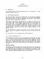
CHAPTER 1
GENERAL INFORMATION
1.1
I NTRODUcr I ON
'Ibis manual provides general information, hardware preparation, prograrrming
considerations, and functional description for the Ml468705EVM Module,
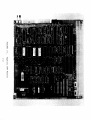
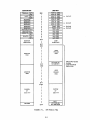
hereinafter called the EVM. A typical EVM is shown in Figure 1-1.
1.2
FEA'IURES
The features of the EVM include:
• Economical means of evaluation for the MC1468705 MCU's
• Requires only power supply and terminal for operation
• Monitor/debugger
• One line assembler/disassembler
• Cassette download/upload
• Host download
• printer port
• Dual memory maps:
4K ROM - monitor map
4K RAM - user map
• Progranmer for on-chip EPROM
• User
~CU
I/O available
• Power-on reset
• User reset/abort switches
• External clock input
• Wire-wrap area
1.3 SPECIFICATIONS
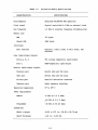
The EVM specifications are identified in Table 1-1.
1-1
1-'
I
N
~......
n
IlJ
1-'
TABLE 1-1.
Evaluation Module Specifications
CHARACTERISTICS
SPECIFICATIONS
Microcomputer
Simulates MC1468705 MCU operation
Clock signal
Crystal controlled 4.0 MHz or external clock
Bus frequency
1.0 MHz or external frequency divided-by-four
Meroory size
112 bytes
Pseudo ROM
3968 bytes
Interrupts
Four vectored
External, timer, timer in wait state, and
software
User input/output signals
Ports A, B, D
TTL
voltage compatible input/output
Port C
CMOS-compatible input/output
Monitor input/output signals
Terminal port
RS-232 (RxD and TxD only)
Host port
RS-232 (RxD and TxD only)
Printer port
Parallel Centronics interface
Cassette port
Audio cassette interface
Operating temperature
00 to 550 C
Power requirements
Module
+5 Vdc at 1.0 A (max)
+12 Vdc at 0.1 A (max)
Programner
-18 Vdc at 50 rnA (max)
Dimensions
Width x height
14.50 x 9.75 in. (36.83 x 24.76
Board thickness
1.20 in. (3.05
1-3
em)
em)
1.4
GENERAL DESCRIPTION
The EVM provides a tool for generating, eXeCU1:1ng, am debugging MCU code. By
providing all of the essential timing and I/O circuitry, the EVM simplifies user
evaluation of the MCU ..
Operation of an MC1468705 MCU is simulated by the resident MC146805G2 MCU. Data
transfer within the EVM is controlled by the monitor RCM firmware.
In turn,
this ROM is controlled from an RS-232C compatible user-supplied terminal. User
object code may be generated using the resident one-line assembler/
disassembler, or may be downloaded to the user program RAM through the host port
or cassette port. User object code may then be executed using various debug
commands in the monitor. Code may also be executed from reset using the USER
RESET switch.
MCU EPRa1 is simulated by write-protecting user program RAM
during program execution.
Simulated MCU parallel I/O ports are available for external connection. These
lines are also used to control the MC1468705 on-chip EPRCM prograrrmer.
The
EPROM is programned am verified by inserting the MC1468705 device into the
correct socket and entering a monitor comnand.
The object code in the user
program RAM is programned into the MCU EPRG1.
Prograrrming is different for each MCU.
The monitor firrrware PR<M must be
changed by the user, depending on which MOJ is to be programned.
A jumper
select option allows either the on-board clock or a user-supplied external clock
to be used. A printer port is provided which is Centronics-compatible. User
circuitry may be added on the wire-wrap area of the module.
Optional kits of firrrware and software are available for operation of the EVM
wi th an EXORset host. The Motorola part numbers for the kits are M68EVMSETG2
aoo M68EVMSETF2.
1-4
CHAPTER 2
HARIMARE PREPARATIoo AND INSTALIATIoo INSTRUerIooS
2.1
INTRODUcrIoo
'!his chapter provides unpacking,
instructions for the EVM.
2.2
hardware
preparation,
and
installation
UNPACKIN:i INSTRUcrIooS
NOTE
If shipping carton is da~aged upon receipt,
request carrier's agent be present during
unpacking/inspection of equipnent.
CAUTION
AVOID
TOUCHING
AREAS
OF
CMOS CIRCUITRY;
STATIC DISCHARGE CAN DAMAGE INTEGRATED CIRCUITS.
Unpack equipment from shipping carton. Refer to packing list and verify that
all items are present.
Save packing material for storing or reshipping the
equipnent.
2 .3
HARIl'UffiE PREPARATION
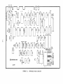
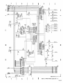
Figure 2-1 illustrates the location of the switches, LED
power connections, and headers on the EVM. The module is
installed jumper configurations. '!he EVM is operational
It is necessary to
wi th the factory-installed jumpers.
jumper arrangements for the following conditions:
indicators, sockets,
shipped with factory(except prograrrming)
make changes in the
a. I/O connector (Jl)
b. Audio cassette playback phase select (J2)
c. HOST port ers and DCD signal enable (JS, J18)
d. User map 2K or 8K select (J8)
e. TERMINAL port and HOST port baud rate select (Jll, J12)
f. write protect disable for user memory (JIO)
g. On-board or external clock select (J13)
h. External clock connection (JI4)
i. EPROM programming select (JIS, J16, J17)
2-1
u
J
"t
--
1-------------
MJ
UA
HOif
".
WIt
'AIN'tR
-'IY
DIID
",
MAP'
"1
,
0
•
:0
.
:0
"
;0
f'..)
I
~.)
,
I
,
0- o
,noo
'
SOD
noo
'III
'.01
2tO.
'200
DO
'00
'0
100
HOD
200
DO
15
15
'ID
'n""
.u,aOD
II
II
""00" UII WtllFJ
'D'a
EIT
ell
IUI7
!o"'4
,..00
AOO
XUSI
i~
DFf~
O'eJ:-~
~
L-_ _ _ _ _ _ _ _ _ _ _ _ _
@
MOTOROLA INC.
,
II ••
_SWOLl
MAS lEa
ann
.,,~
c,
©,g'!I
-------.~u
••
FIGURE 2-1.
Option Locations
I
2.3.1
I/O Connector (Jl)
The I/O connector may be used as a convenient means of connecting user circuitry
to MC1468705 interrupt and timer inputs and port C I/O. The I/O connector also
connects to the simulated user I/O port A, port B, am port D. Signal names
shown in Figure 2-2 are the MC1468705 equivalent.
In
J1
PAO
4
6
8
10
12
14
16
PAl
PA3
PA5
PA7
PBl
PB3
PB5
PB7
NC 19n2O
TMR 21 I 0 0 , 22
IRQ
NC
PCO
PC2
PC4
PC6
POO
P02
P04
P06
PCl
PC3
PC5
PCl
PA2 3
PA4 5
PA6 7
PBO 9
PB2 11
PB4 13
PB6 15
25
27
29
31
33
35
37
39
FIGURE 2-2.
0
0
0
0
0
0
0
0
0
0
0
0
0
0
2
0
0
0
0
0
0
0
0
26
28
30
32
0
0
J'f
PDi
0
0
0
0
0
0
36
38
40
P03
P05
POl
.... II
I/O Connector (Jl)
2-3
2.3.2
Audio Cassette Playback Phase Select Header (J2)
Some audio tape cassette recorders invert the recorded signal. Header J2 allows
the signal to be inverted to a compatible phase for the EVM.
The EVM is
factory-configured with the jumper positioned between pins I and 2 for a noninverted playback signal (see Figure 2-3).
For a recorder with an inverted
playback signal, position the jumper between pins 2 and 3.
PH
J2
:rn
FIGURE 2-3.
2.3.3
Audio Cassette Playback Phase Select (J2)
HOST Port (J4) CTS and DCD Signal Enable Headers (J5, JI8)
The EVM is shipped with the HOST port (J4) CTS and DCD input signals held high,
and with the jumpers on header J5 and JI8 positioned between pins I and 2 (see
Figure 2-4). Should the host computer or modem have full handshake capability,
the jumpers may be positioned between pins 2 and 3 on headers J5 and JIB.
J5
J18
:rn :rn
FIGURE 2-4.
HOST port (J4) CTS and DCD Signal Enable Headers (J5, JIB)
2-4
2.3.4
User Map 2K or 8K Select Header (J8)
Header J8 allows the user to select between a 2K user map for evaluating an
MC1468705F2 and an 8K user map for evaluating an MC1468705G2.
The EVM is
factory-configured in the 8K mode with the jumper between pins I and 2 (see
Figure 2-5).
MAP
J8
:: m:
FIGURE 2-5.
2.3.5
User Map 2K or 8K Select Header (J8)
Write Protect Disable Header (JIO)
The EVM is shipped with the jumper between pins I and 2 (see Figure 2-6), which
wri te protects the user program space 080-FFF during user program execution
(pseudo R~). To disable the write protect function, move the jumper to between
pins 2 and 3.
J10
:rn
FIGURE 2-6.
Write Protect Disable Header (JIO)
2-5
2.3.6
TERMINAL Port and HOST Port Baud Rate Select Headers (Jll, J12)
Headers Jll and J12 are provided to allow the baud rates to be set for
compatibili ty with the user terminal and host computer. The EVM is factoryconfigured with the jumpers positioned for 9600 baud rate operation (see
Figure 2-7). For other baud rate operation, refer to Figure 2-7.
In the transparent mode, which allows direct comnunications between the terminal
aoo the host, the host computer baud rate should be set one increment lower
than the terminal (e.g., terminal 2400 = host 1200). If both baud rates are the
same, a character may be lost occasionally by the terminal. Ibwnload is not
affected by equal baud rates on the host and terminal.
TERMINAL BAUD
RATE
HOST BAUD
RATE
Jll
1
0
J12
0
0-0
0
0
0
0
lj
0
15
FIGURE 2-7.
2.3.7
0
o
0
0
0
19200
9600
4800
2400
1200
1
0
0
0--0
,..""
ouu
0
0
0
0
0
0
lj
300
110
o
15 o
0
0
19200
9600
4800
2400
1200
600
300
110
TERMINAL Port and HOST Port Baud Rate Select Headers (Jll, J12)
On-Board or External Clock Select (JI3)
The on-board clock source is a 4 MHz crystal. The EVM is factory-configured for
4 MHz operation with the jumper positioned between pins 2 and 3 (4 MHZ) on
header J13 (see Figure 2-8).
Should the user wish to use a user-supplied
external clock, the jumper should be positioned between pins 1 and 2 (EXT). The
EXT position is used in conjunction with header J14.
E J13
;m
1
3
Z
FIGUHE 2-8..
CD-Board or External Clock Select (J13)
2=6
2.3.8
External Clock Connection (JI4)
A two-pin header is provided for connection of an external TTL compatible clock
(see Figure 2-9). Header pin 2 is ground (GND).
EXT
elK
~~
J14
FIGURE 2-9.
2.3.9
External Clock Connection (JI4)
EPROM programming Select Headers (JIS, J16, J17)
The EVM is designed to program the MC146870SG2 and MC146870SF2. Headers are
provided to connect the three control lines needed to handshake with the
MC1468705 during programming. These three lines are also user port D lines
(PDQ, PDl, PD3 on Jl). Jumpers positioned between pins 1 and 2 on headers
JIS-J17 disconnect the loading effect of the programmer from user I/O port D.
The EVM is shipped with the four jumpers in the disconnected position (see
Figure 2-10). Refer to Chapter 3 for programming information.
ji5
jj
6
J17
:rn :rn :rn
PROG
FIGURE 2-10.
2.4
PROG
PROG
EPROM programming Select Headers (JIS, J16, J17)
INSTALLATION INSTRUCTIONS
The EVM is a stand-alone system which is designed for table-top operation. A
user-supplied power supply is required for operation and programning. A usersupplied terminal is required for entering and changing data. A host computer
(e.g., EXORciser), a printer, and/or an audio cassette may be connected, but are
not required for normal operation (see Figure 2-11).
2-7
TERMINAL
M1468705EVM
AUDIO
CASSETTE
RECORDER
POWER SUPPL Y
FIGURE 2-11.
System Configurations
2-8
2.4.1
Power Supply Installation
The EVM requires +5 Vdc @ 1 A, +12 Vdc @ 0.1 A, -12 Vdc @ 0.1 A for operation,
and -18 Vdc @ 50 rnA for programming. A reccmnended power supply for +5 V, +12 V
is a Comor model TAA-16W. The -18 programmirg voltage may be supplied by two
9 V batteries or a good -18 V, 50 rnA power supply.
The terminal block PIon the EVM is designed for 14-22 AWG wire.
2-12 for connections.
See Figure
PI
+5V
GND
+12V
GND
-12V
FIGu~E
2.4.2
2-12.
m
'"
(S)
e
GND
0
-18V
(S)
Power Supply Installation
Terminal Installation
An RS-232C compatible tenninal is required to enter data, debug a user program,
print data, am program an t-CU EPROM. ,Most terminals can be connected to the
EVM with a cable requiring a 20-contact edge connector on the EVM end and a
25-contact D-type subminiature connector on the terminal end. The subminiature
connector can be either pin (male) or socket (female), as required by the user
tenninal. Both of these cable types are available from Motorola:
PART NUMBER
DESCRIPTION
M68RS232M
RS-232C Cable, Edge/Male
M68RS232F
RS-232C Cable, Edge/Female
The user may manufacture a cable suitable for this purpose. Figure 2-13 shows a
detail of the cable, lists several suitable vendor part numbers (any equivalent
part may be used), am shows the comuctor line designations present on the EVM.
The cable requires a 20- or 25-conductor flat ribbon; connectors should be
installed accordirg to manufacturer's instructions. The edge connector may be
keyed to prevent incorrect cable connection.
The cable is connected between the EVM edge connector J3 (TERMINAL) and the user
tenninal. Be sure to orient pin 1 of the cable with pin 1 of J3.
20 OR 25 CONDUCTOR
FLAT RIBBON
CABLE
3M "3365-20
OR
3M "3365-25
KEY
(OPTIONAL)
~ ~o
r-----------wl I
I
25 "0" SUBMINIATURE MALE
(PIN) CONNECTOR
PART ,'S:
25 "0" SUBMINIATURE FEMALE
(SOCKET) CONNECTOR
PART ,'S:
20 CARD EDGE CONNECTOR
PART ,'S:
1. CIRCUIT ASSEMBLY CORP
1. CIRCUIT ASSEMBLEY CORP
2. ANSLEY H09·2015 M
.CA·25·SMO·P
1. AM P '88373·6
'CA·25·SM O·S
2. ITT CANNON "DBSP-B25P
2. ITT CANNON "DBSP-B25S
3. ANSLEY 1609·25P
3. ANSLEY 1609·25S
4. WINCHESTER '49·1125P
4. WINCHESTER '49·1125S
3. BERG "5164·002
4. 3M '3461·0001
25 PIN "0" SUBMINIATURE CONNECTOR
Q
Z
CJ
-'
c
c
z
~
Q
)(
II:
\1
1\ 14
3
2
15
.
4
5
17
16
6
CJ
oQ
7
8
11
10
9
21
20
19
18
Q
iii
24
23
22
RED(..
\
1~
12
.25
J
II III
v
NOT CONNECTED
1
3
5
7
9
11
13
15
17
19
2
4
6
8
10
12
14
16
18
20
20 PIN CARD EDGE CONNECTOR
FIGuKE 2-13.
Terminal Cable Details
2-10
I
2.4.3
Host Computer (Modem) Installation
The EVM can be operatErl with a host computer directly or by rrodem. The host
computer (e.g., EXORciser) or modem is connected to the EVM with a cable which
is similar to the terminal cable.
Refer to paragraph 2.4.2 for details of
purchased or user-manufactured cable.
The edge connector may be keyed to
prevent incorrect cable connection. Figure 2-14 shows the host computer cable
signal line connections which are present on the EVM.
The cable is connectErl between the EVM edge connector J4 (HOST) and the user
host computer or modem. Be sure to orient pin 1 of the cable with pin 1 of J4.
25 PIN "D" SUBMINIATURE CONNECTOR
Q
Z
o
....
c
z
o
c
~
Q
)(
en
~
\
\
15
14
4
3
2
16
5
7
19
18
17
I
RED-c..
6
~
~
Q
Q
(.)
Q
21
20
I
10
9
8
22
I 23 1i
I
\
I I1
112
v
NOT CONNECTED
I
1
3
5
7
2 /'
4 /
6'/
8./
9
10 /
11
13
15
17
19
12 . /
14 /
16'/
18 / '
20 / '
20 PIN CARD EDGE CONNECTOR
FIGURE 2-14.
Host cable Signal Line Connections
2-11
I
I
2.4.4
Printer Installation
designw to drive any Centronics interface printer. wnen purcnasea
from Motorola, the printer is supplied with a cable. The cable may be purchased
from Motorola by ordering part number MEX68PIC.
".rne ErVM is
The user may manufacture this cable, although it is a more complex assembly than
ribbon cable and connectors. Figure 2-15 shows the interconnection diagram of
the cable and lists suitable connector part numbers. The cable may be keyed on
the edge connector to prevent incorrect cable connection.
The cable is connectoo between the EVM ooge connector J9 (PRINTER) and the user
printer. Be sure to orient pin 1 of the cable with pin 1 of J9.
2.4.5 Audio Cassette Player Installation
An audio cassette player may be used to save program object code from the EVM.
Two signal lines plus ground must be connectoo to the cassette player from EVM
J6 (EAR) and J7 (MIC). An inexpensive cassette player, GE model 3-5153, may be
used.
The user must buy or make a cable sui table for the cassette player used. An
audio patch cord (Radio Shack part number 42-2420) and an adapter (Radio Shack
part number 274-327) may be used with most recorders which use miniature phone
plugs.
The cassette player is connected to the EVM by connecting the adapter to EVM J6
or J7 and the pa tch cord between the adapter and the cassette player. The data
out signal at EVM J7 (MIC) should be connected to the MICROPHONE input of the
cassette recorder for saving programs.
The data in signal at EVM J6 (EAR)
should be connected to the EARPHONE output of the cassette player for loading
programs into the EVM memory. ~ound connections are part of the patch cords.
2-12
EXAMPLE:
3M "3415·0001
FLAT RIBBON
CABLE
EVM
39
40
37
38
35
36
33
34
31
32
29
30
27
28
25
26
43
44
47
48
DATA 1
PRINTER
2
DATA 1 RTN
20
DATA 2
3
DATA 2 RTN
21
DATA 3
4
DATA 3 RTN
22
DATA 4
5
DATA 4 RTN
23
DATA 5
6
DATA 5 RTN
24
DATA 6
7
DATA 6 RTN
25
DATA 7
8
DATA 7 RTN
26
RTN
9
RTN
D~T~
EXAMPLE:
AMPHENOl "57·10360·13
CINCH "57·10360
27
STB
1
DATA STe RTN
19
~
10
ACK RTN
28
FIGURE 2:-15.
Printer Cable Interconnection Diagl:am
CHAPTER 3
OPERATING INSTRUCTIONS
3.1
INTRODUCTI ClJ
This chapter describes the operating procedures, MCU
procedures, and the debug/monitor commands for the EVM.
3.2
EPROM
programming
SWITCHES AND INDICATORS
The EVM is provided with five switches and four LED indicators. The indicators
show the status of certain functions during EPROM programming, and may prompt
the user to perform some function. See Figure 2-1 for location of switches and
indicators.
3.2.1
Switches
Two switches (Sl, S2) control the user reset and abort functions of the module.
Two switches (S3, S4) control the EPROM programming operation, together with the
LED status indicators. A master reset switch (S5) is also provided.
USER RESET
- The USER RESET pushbutton switch (Sl) , located on the upper left
corner of the EVM, is used to reset the MPU and all user I/O, and
swi tch to the user map. The USER RESET swi tch may be used as a
permanent map switch for execution of user code from the user
reset vector (see user map description) •
ABORT
- '!he ABORT pushbutton switch
PROGRAM
- The PROGRAM slide switch (S3) , located on the lower right corner
of the EVM, is used to activate +12 Vdc and +27 Vdc power used to
program the EPROM. LED indicator (CR7) is lit when this switch
is in the ON position.
+5VOLT
- The +5VOLT slide switch (S4) , located on the lower right corner
of the EVM, is used to activate +5 Vdc power used during the
programming and read operations. LED indicator (CRa) is Ii t when
this switch is in the ON position.
(S2) , located on the upper left
corner of the EVM, is used to return to the monitor map from the
user map (see user map description). The ABORT switch has no
effect when operating in the monitor map.
MASTER RESET - The MASTER RESET switch (S5) , located on the lower left of the
EVM, is used to perform a power on reset of the entire EVM.
3-1
3.2.2 Indicators
Four LED indicators show the status of the programmer circuitry.
PROG
Red LED indicator (081), when lit, informs the user that the device in
socket XU56 or XU57 is being programmed.
VERF
Red LED indicator (082), when lit, informs the user that the device in
socket XU56 or XU57 has been programmed and verified.
PROGRAM - Red LED indicator (083), when lit, informs the user that PROGRAM
switch (83) is in the ON position, applying -12 Vdc and -18 Vdc to the
device to be programmed.
+5VOLT - Red LED indicator (D84) , when lit, informs the user that +5VOLT switch
(84) is in the ON position, applying +5 Vdc to the device to be
programmed or read.
3.3 MEMORY MAP CONCEPT
The EVM is designed to operate in either one of two maps (monitor map or user
map). The monitor map contains 4K bytes of RAM/ROM which includes the monitor
ROM, monitor RAM/stack, monitor I/O, a monitor control register, and a user
stack pointer (see Figure 3-1). The user map, which simulates the MC1468705
memory map, contains the user I/O ports, user RAM/stack, and user pseudo RCJv1
(see Figure 3-1).
The memory maps are decoded with a field programmable gate array.
NOTE
The entire 4K-byte memory map is available to the user,
although all MC1468705 MCU devices do not have EPROM
throughout the entire 4K-byte map.
Refer to the
specific device data sheet for valid program locations.
3.3.1 Monitor Map
The terminal, host, cassette, and printer ports are available only in the
monitor map. User programs in the user map can not access the peripheral ports.
3.3.2 User Map
All user I/O ports lfi, S, C, D) are available in b~e user map for evaluation.
All ports are reconstructed off chip except port C.
User pseudo ROM - The user progrc?-m space (080-FFF) is RAM, which is write
protected during user program execution. This feature requires all programs to
be ROMable and protects against program errors which would otherwise overwrite
the program space.
Header J8 on the EVM provides a simulated 8K user map for evaluating the
MC146870SG2, and a simulated 2K user map for evaluating the t-K!1468705F2.
Although the EVM has only a 4K map, the user vectors fetched from IFF6-lFFF or
7F6-7FF for the MC146870SG2 arrl MC146870SF2, respectively, appear to the ~I.M MCU
at lFF6-lFFF. This is accomplished by shadowing the lower 4K map into the upper
4K map (8K option), or by multiple shadowing the lower 2K map into the upper 6K
map (2K options).
3-2
USER IIAP
IIONITOR IIA'
TERMINAL - CNTL
- DATA
HOST - CNTL
-DATA
RESERVED
RESERVED
RESERVED
RESERVED
RESERVED
RESERVED
USER STACK PNTR
MONITOR CNTL
CASSETIE - DATA
-CNTL
PRINTER - DATA
-CNTL
MONITOR
RAM/STACK
PORT A PORT B PORT C PORT D PORT A-
$000
1
2
3
4
5
6
7
DATA
DATA
DATA
DATA
DDR
-
ON CHIP
PORT B - DDR
PORT C - DDR
A
PORT D - DDR
TIMER - DATA
TIMER - CNTL
NOT USED
B
C
NOT USED
NOT USED
D
E
NOT USED
NOT USED
F
$010
NOT USED
•
•
USER
RAM/STACK
8
9
ON CHIP
ON CHIP
ON CHIP
$07F
$080
•
•
•
MONITOR
ROM
USER
PSEUDO
ROM
•
•
•
•
•
•
•
•
VECTORS (2K)
MC1468705F2
$7FF
$800
MONITOR
ROM
•
•
•
•
•
•
•
•
•
•
USER
PSEUDO
ROM
$FFF
$1000
SHADOW
OF
OOO-FFF
VECTORS
•
•
•
•
•
•
•
•
•
•
•
•
VECTORS (4K)
$1FFF
MC1468705G2
FIGURE 3-1.
SHADOW
OF
OOO-FFF
MOR
EVM Memory Map
3-3
WRITE-PROTECTED
DURING
USER PROGRAM
EXECUTION
3.4
MAP SWITCHES
IVN
types of map switches are provided -- a ternfAjrary' swi ten which allows
modification of user memory under monitor control, .and a permanent switch which
allows execution of user programs&
3.4.1
Program Execution
A permanent map switch for execution of user code can be initiated in two ways:
Command from the monitor
The monitor commands G (execute from address), P (proceed from breakpoint), and
T (trace instructions) allow execution of user programs.
Pressing the USER RESET switch (Sl)
When the USER RESET switch is pressed, the MCU and all user I/O are reset, maps
are immediately switched to the user map, and the reset vector is fetched from
the user map by the MCU. Breakpoints are ignored during this mode of execution.
Execution can be halted only with the ABORT switch.
Return to monitor control occurs in two ways:
A breakpoint or the end of a trace function in the monitor
Execution of user code continues until a breakpoint (SWl) is encountered or the
ABORT switch is pressed. The map is switched back to the monitor map after the
registers are saved on the user stack. An SWI which occurs when no breakpoint
is set -- and when the ABORT switch is not being pressed -- does not cause a map
switch. This allows user SWI's to be executed in real time.
pressing the ABORT switch (S2)
The ABORT switch, when pressed, forces an SWI on the data bus until the next
LIR. The registers are saved on the user stack and maps switched to the monitor.
The ABORT switch has no effect on the monitor map.
3.5
LIMITATI(l.JS
protection is provided to limit programs to the exact aIOOunt of EPROM
'!he user must be aware of ~'1e map of the MCU being evaluated and
ensure that only valid EPROM locations are used.
No
avai lable.
AI though an external clock input may be used to evaluate the MCU at reduced
speeds, LOAD, TPLD, and TPDU functions may be used only while operating at full
I-MHz rate. TO operate at reduced speed with an external clock, the following
procedure should be performed.
a. Load the program (LOAD, TPLD, or TPDU commands) at full I-MHz clock rate.
b. Press and hold the MASTER RESET switch while positioning the jumper at
J13 to pillS 1 and 2.
~~'hen
the Jumper is in place, release the
RESET swi tch •
3-4
~~tSTER
c. The user program can now be executed and debugged at reduced clock speed.
d. To return to full clock rate, repeat steps band c moving jumper on
header J13 to pins 2 and 3.
'!he baud rates of the terminal and host are independent; however, during
transparent 100de , characters from the host computer to the terminal may
occasionally be lost if the terminal baud rate is not higher than the host baud
rate. This occurs only during the transparent mode, and does not apply when
downloading to memory.
'!'he audio cassette format is unique to the EVM and is not compatible with any
other tape format.
The printer port does not support any of the error detect lines.
strobe, and acknowledge lines are implemented.
3.6
Only the data,
OPERATIKl PROCEDURE
'!'he monitor is the resident firmware for the EVM, which provides a selfcontained programming and operating environment. '!he monitor interacts with the
user through predefined commands that are entered from a terminal. The commands
fall into five general categories:
a. Commands which allow the user to display or modify memory.
b. Commands which allow the user to display or modify the various internal
reg isters of the MCU.
c. Commands which allow the user to execute a program under various levels
of control.
d. Commands which control access to the various input/output peripherals
connected to the EVM.
e. Commands which program or read the MCU EPROM.
The monitor requires five bytes of user stack for user register storage on
monitor (re) entry. No limitation is placed on the user as to other uses of the
stack.
All user registers are in an unknown state on monitor power-up.
3.6.1
System Initialization
Turning power on initializes the EVM system.
invoked. '!'he terminal displays:
EVMbug705 REV X.XX
s=xx
A=XX
c=XX
The MCU is reset and the monitor
X=XX
P=XXXX
?
where X is a revision of the software or an unknown register state.
Other means can be used to reinitialize the EVM finnware (see paragraph 3.2.1) •
3-5
3.6.2
System Operation
initialization or
the prompt ? and waits for a response. If an invalid response is entered, the
terminal displays a "What?", and rings the bell.
A dollar sign ($) may precede any number input except bit number specifications
in the BCLR/BSET and BRCLR/BRSET assembler mnemonics.
All numbers are
interpreted as hexadecimal -- the ($) is not required.
The user can call any of the commands supported by the monitor. A standard
input routine controls the system while the user types a line of input. Command
processing begins only after the line has been terminated by a carriage return
(see note 6, paragraph 3.6.3).
.
3.6.3 Command Line Format
The command line format is:
? [NO]<command> [<parameters>]
where:
?
Is the prompt from the EVM monitor.
NO
Is
commaoo
Is the primitive command.
parameters
Are separated by a single space.
~~e
negative (opposite) of some primitive
co~mands.
NOTES
1. The command line format is defined using special characters
which have the following syntactical meanings:
< >
Enclose a syntactical variable.
Enclose optional fields.
] •••
Enclose optional fields which may be repeated.
These characters are not entered by
definition only.
~~e
user, but are for
2. Fields are separated by a single space.
3. A maximum of 30 characters may be entered on a command
line. After the 30th character is entered, the monitor
automatically terminates the line and begins processing
~~e 3D-character line.
... ,.
"-0
4. RETURN (CR) (carriage return) enters the command line
and causes processing to begin.
5. CTRLrX cancels the entire input line.
6. Parameters are interpreted to be the last two or three
characters in the parameter field. Parameter errors may
be corrected by re-entering the parameter without a space.
3.6.4 primitive Oommands
Monitor primitive commands are listed in Table 3-1.
TABLE 3-1.
Moni tor Primi ti ve Oorrmands
DESCRIPTION
ASM <address>
Assembler/disassembler (interactive)
BF <addressl> <address2> <data>
Block fill memory with data
[NO]BR [<address>] •••
Breakpoint set/reset/remove
G [<address>]
Go
LOAD [<offset>]<= text>
Download memory (S-records) from host file
MD <addressl> [<address2>]
Memory display
MM <address>
Memory modify (interactive)
P [<count>]
proceed (from breakpoint)
[NO] PA
printer attach/reset printer attach
PRo:;
progr am EPROM
RD
Register display
READ
Read EPROM contents
RM
Register modify (interactive)
T [<count>]
Trace (instructions)
TM [<exit character>]
Transparent mode
TPDU <addressl> <address2>
Dump memo ry to cassette tape
TPLD [<offset>]
Load memory from cassette tape
(execute program)
Each of the individual commands is described in the following paragraphs.
3-7
3.6.5
ASM
Assembler/Disassembler (Interactive)
ASM <address>
where <address> is the starting address for the assembler operation.
'!he assembler/disassembler is an interactive assembler/editor in which the
source program is not saved. Each source line is translated into the proper
machine language code and is stored in memory on a line-by-line basis at the
time of entry.
In order to display an instruction, the machine code is
disassembled and the instruction mnemonic and operands are displayed. All valid
instructions are translated.
The ASM command allows the user to create, modify, and debug MC6805 code.
provision is made for line numbers or labels.
No
Assembler input must have exactly one space between the mnemonic and the
operand. There must be no space between the operand and the index specification
( ,X) except in the case of indexed no offset.
Assembler input must be
terminated by a carriage return.
No comments, etc., are allowed after the
instruction input.
EXAMPLE:
a ..
b.
c.
d.
e.
?LDA ,X
?STA 10,X
?BRCLR 3,$52,200
?COMX
?CMP 200
After each new assembler input line, the new line is disassembled for the user
before stepping to the new instruction.
'!he new line may assemble to a
different number of bytes than the previous one.
It is left to the user to
watch for this.
Each of the instruction pairs ASLA/LSLA and ASLX/LSLX have the same opcode, so
disassembly always reveals LSLA or LSLX, respectively.
A dollar sign ($) may precede any number input except bit specifications in the
BCLR/BSET and BRCLR/BRSET assembler mnemonics.
The assembler is terminated by entering a period (.) followed by a carriage
return. Entering a carriage return alone on an input line steps to the next
instruction.
Entering crRL X cancels an input line.
roode.
'!he moni tor remains in the assembler
EXAMPLE
?ASM 200
0200 FF
0200 OE 10 OD
0203 FF
0203 A6 55
0205 FF
0205 F7
0206 FF
0206 CE 06 1:11
0209 FF
'C't;"
0209 20 J.',u
020B FF
";":1;
?BRSET 7,10,210
BRA
,X
7,$10,$0210
,X
#$55
,X
,X
,X
$0654
,X
$0209
STX
,X
?
STX
BRSET
STX
LOA
STX
STA
STX
LDX
STX
?LOA #$55
?STA ,X
?LOX 654
?BRA 209
3-8
3.6.6
Block Fill Memory with Data
BF
BF <addressl> <address2> <data>
where:
addressl
Is the lower limit for fill operation.
address2
Is the upper limit for fill operation.
data
Is the fill pattern hexadecimal value.
'!he BF corrmand allows the user to repeat a specific pattern throughout a
determined user memory range.
Caution should be used when modifying locations O-F or 60-7F. The user I/O
configurations and interrupt masks are located at O-F. 60-7F contain the user
stack area. The user registers are stored in the five bytes immediately below
the user stack.
No operation is performed if addressl is greater than address2.
EXAMPLE
C(}1MENTS
?BF 101 200 FF
Fill each byte of memory from 101 through 200 with
the pattern FF.
?BF 10 10 0
Sets location 10 to
3-9
o.
3.6.7
Breakpoint Set
Breakpoint Remove
BR
NOSR
BR [<address>] •••
NOSR [<address>]
The BR corrunand enters the address into the internal breakpoint table. During
execution of the user program, a debug halt occurs immediately preceding the
execution of any instruction address in the breakpoint table.
The NOBR command is used to remove one or all breakpoints from the breakpoint
table.
User should not put a breakpoint on an SWI instruction as this is the
instruction that the monitor uses to breakpoint/single-step a user program. The
user may use the SWI instruction in the user program.
When a new breakpoint is entered, the breakpoint table is fi rst cleared.
maximum of three breakpoints may be set.
A
After setting or removing a breakpoint, the current breakpoint addresses, if
any, are displayed~
CavlMAND FORMAT
DESCRIPTION
BR
Display all current breakpoints.
BR <address>
Set a breakpoint.
BR <addressl> <address2> •••
Set several breakpoints.
NOBR
Remove all current breakpoints.
NOBR <address>
Remove a breakpoint.
EXAMPLE
CCtJlMENTS
?SR 080
Sets a breakpoint at 080.
?BR 084 09A 984
Sets three breakpoints.
?NOBR
Removes all breakpoints.
?BR
Displays all current breakpoints.
3.6.8 Go (Execute program)
G
G [<address>]
where:
address
Is the starting address where execution begins.
The G command allows the user to initiate user program execution in free run in
real time. The user may optionally specify a starting address where execution
is to begin.
Execution starts at current PC unless starting address is
specified. Program execution continues until a breakpoint is encountered or the
ABORT switch is pressed.
EXAMPLE
?G
Begin execution at current PC location.
?G 100
Begin execution at location 100.
3-11
3.6.9
Download Memory (S-Records) from Host File
Lew)
LOAD [<offset>]<=text>
where:
offset
Is the optionally specified offset to be applied to all load
addresses retrieved from the loaded S-records.
=text
The text following the = is a host command sent to the host
port, which instructs the host to download S-records.
The load command moves object data in S-record format (see Appendix A) from an
external host to memory.
When loading data from a host file, the data received by the monitor is echoed
to the terminal so that the user may monitor the load progress. 8-records are
not echoed to the printer due to timing considerations.
If the terminal is
running at a baud rate less than the host, the S-record echo may be scrambled
but the data is entered correctly to memory.
As the moni tor processes only valid S-record data, it is possible for the
monitor to hang up during a load operation (there is no internal timeout because
the terminal and host may be running at different baud rates) ~ Therefore: prior
to the load operation, the user should define a reset vector to execute a
branch-to-self instruction. Then, if the monitor should become hung up during a
load operation, the user may do a reset/abort on the processor and return the
monitor to the command state.
The load operation may optionally specify an offset to be applied to all load
addresses retrieved from the loaded S-records.
No check is made that the
address does not rollover from high memory to low memory after adding the
offset.
EXAMPLE
CC»1AND
?LOAD =COPY FILE.LX:l,#CN
Loads the data from the host (EXORciser) to
the EVM.
?LOAD lOO=COPY FILE.MX;#
Loads; with offset; the data from th.e host
(EXORmacs) to the EVM.
3.6.10
Memory Display
MD
MD <addressl> [<address2>]
where:
addressl
Is the beginning address of the memory to be displayed.
address2
Is the ending address of the memory to be displayed.
The MD command is used to display a section of memory beginning at addressl and
continuing to address2.
If address2 is not entered I 16 bytes are displayed
beginning at addressl.
No operation is performed if addressl is greater than address2.
EXAMPLE
?MD 100 110
100 OC 00 00 30 6D 28 OC 00 00 39 6E 10 02 80 00 00
••• Om( ••• 9n •••••
110
00 OF 11 CO 10 38 IE 3C 00 E4 4E 4E OC 00 00 41
••• @.8.<.dNN ••• A
?MD lOA
lOA
6E 10 02 80 00 00 00 OF 11 CO 10 38 IE 49 00 E4
3-13
n •••••••••• 8.< ••
3.6.11 Memory Modify (Interactive)
MM
MM <address>
where:
address
Is the memory location at which to start display/modify.
The MM command allows the user to examine/modify user memory locations in an
interactive manner.
Caution should be used when modifying the user stack area because the user
registers are stored in the five bytes immediately below the user stack.
Once entered, the MM command has several submodes of operation that allow
modification and verification of data.
'!he following terminators are
recognized.
[<data>] (CR)
- Update location and sequence forward.
[<data>]~(CR)
- Update location and sequence backward.
[<data>] =(CR) - Update location and reopen same location.
[<data>] • (CR) - Update location and terminate.
An
entry of only ". (CR) " terminates the register modify interactive mode.
CTRL X may be used to cancel any input line; the moni tor remains in the MM
conunand.
EXAMPLE
CG1MENT
?MM 100
OlOO=FF?OO=
0100=00?
OlOO=FF?OO=
0100=00?-.-
Display memory location 100, modify FF to 00,
display same location" then terminate.
3-14
and
3.6.12 Proceed (from Breakpoint)
P
P [<count>]
Ylbere:
count
Is the number (in hexadecimal) of times the current
breakpoint location is to be passed before the breakpoint
returns control to the monitor.
All other breakpoints are ignored during this command.
EXAMPLE
?P 5
3-15
3.6.13
Printer Attach
Printer Detach
PA
NOPA
PA
NOPA
The PA command allows the user to software attach the line printer so that
information sent to the terminal is also printed. The printer is physically
attached to EVM J9 (PRINTER).
The NOPA command allows the user to detach the printer from the terminal.
The PA command should only be entered when a printer is physically connected to
the EVM. Otherwise, the monitor hangs up while waiting for a response from the
printer. To recover from this hang up , the printer must be attached, the power
removed from the EVM, or the MASTER RESET switch (S5) pressed.
3-16
PRCG
3.6.14 Program EPROM
PRO;
The PROG command is used to program the MC1468705 MCU internal EPROM. Prior to
entering this command, jumpers must be positioned, switches must be set, and the
unprogrammed MCU installed in the proper socket. paragraph 3.7 describes the
procedure for programming the EPROM in detail. Because of the limited monitor
memory size, only the MC1468705G2 can be programmed with the G2 version of the
monitor program, and only the MC1468705F2 can be programmed with the F2 version
of the monitor program.
3-17
3.6.15
Register Display
RD
RD
. The RD command displays the MCU register contents.
CQ\1MAND FORMAT
DESCRIPTION
?RD
The contents of the following registers are displayed:
S = stack pointer
C = condition code
A = accumulator
X = index
P = program counter
EXAMPLE
?RD
S=7F
C=FA
A=FF
X=lO
P=0047
3-18
3.6.16
Read EPROM Contents
READ
READ
The READ command allows the user to display the contents of the programmed
internal EPROM of the MC1468705 MCU.
paragraph 3.8 describes the procedure for reading the programmed EPROM.
3-19
3.6.17
Register Modify (Interactive)
RM
RM
The RM command is used to modify the MPU registers. The RM command takes no
parameters and starts by displaying the S (stack pointer) register and then
displaying the C (condition code) register and allowing changes to be made to
the condition code register. The order of the register display follows:
modification allowed; moves to next line.
S (stack pointer)
- No
C (condition code)
- Only bits 0-4 are significant.
A (user A register)
X (user X register)
p (program counter) - Two, bytes displayed/allowed.
The user may not change the stack pointer using the RM command.
Once entered, the RM command has several subnodes of operation that allow
modification and verification of data.
The following terminators are
recognized.
- Update register and sequence forward.
- Update register and sequence backward.
- Update register and reopen same location.
- Update register and terminate.
[<data>] (CR)
[<data>] (CR)
A
[<data>] = (CR)
[<data>] .- (CR)
M entry of only
II.
(CR) II terminates the register modify interactive mode.
The user may use CTRL-X to cancel any input line; the monitor remains in this
corrmand.
EXAMPLE
?RM
S=7D
C=OO?CC
A=AA?FE=
A=FE?
X=10?77
P=0056?100"
X=77?
?=RD
Regs
S=7D
COOMENT
Command entered.
Shows S status and skips to C.
Change C register.
Change A register. Re-examine register.
Look at A register change.
Change X register.
Change P register. Sequence backward.
Look at X register. Terminate command.
Enter RD command.
C=CC
A=FE
X77
P=0100
3-20
3.6.18
Trace
T
T [<count>]
where:
count
Is the number (in hexadecimal) of instructions to execute.
The T command allows the
instruction basis. The
time by entering a count
The PC displayed with
executed.
user to monitor program execution on an instruction-byuser may optionally execute several instructions at a
value (up to FF) • Execution starts at the current PC.
the event message is of the next instruction to be
During the tracing operation, breakpoints are active and user program execution
stops upon the PC encountering a breakpoint address. Depending upon the user
program execution results, the monitor issues one of the following target status
messages before displaying a prompt for the next user input.
Trace
S=nn
C=nn
A=nn
X=nn
P=nnnn
Brkpt
S=nn
C=nn
A=nn
X=nn
P=nnnn
The user should not try to trace an instruction that branches to itself (eege;
BRCLR Y,XX,*). Because the monitor puts an SWIT instruction on the object of the
branch, the instruction would never be executed. However, it would look to the
user as if the instruction executes. The user may enter a G command while the
PC points to this type of instruction as long as the instruction is not at a
breakpoint address.
The monitor issues an error message if the user attempts to trace at an address
that contains an invalid opcode.
CCl4MENT
EXAMPLE
?T
Trace
S=7D
C=FC
A=OO
X=lO
P=OO51
Single trace.
?T 5
Trace
Trace
Trace
Trace
Trace
S=7D
S=7D
S=7D
S=7D
S=7D
C=FA
C=FC
C=FC
C=FA
C=FC
A=OO
A=OO
A=OO
A=OO
A=OO
X=lO
X=lO
X=lO
X=lO
X=lO
P=OO54
P=OO56
P=OO51
P=OO54
P=OO56
3-21
Multiple trace with count
of 5 entered.
3.6.19
Transparent Mode
TM
TM [<exit character>]
where:
exit character
Is the user entry to terminate the transparent mode.
The TM conunand connects the EVM host port to the terminal port, which allows
direct conununication between the terminal and the host.
All input/output
between them is ignored by the EVM until the exit character is entered from the
terminal.
When the TM command is entered, an exit character is entered following the TM
(e.g., ?TM 1). The exit character can be any keyboard character (printable or
non-printable). The default exit character is CTRL-A. When the user task is
completed, the transparent roode is terminated by entering the same exi t
character.
EXAMPLES
C~
?1M
Command followed by a carriage return.
character. MOOS program entered.
MOOS
CTRL-A is default exit
=DIR
=CTRL-A
?
Task complete.
terminated.
Enter exit character CTRL-A.
Transparent mode
Command followed by exit character (1). MOOS program entered.
Directory called up.
Task complete.
terminated.
Enter exit character (1).
3-22
Transparent mode
3.6.20
Dump Memory to Cassette Tape
TPDU
TPDU <addressl> <address2>
where:
addressl
Is the beginning address of the memory to be dLUnped.
address2
Is the ending address of the memory to be dumped.
The TPDU corrunand outputs memory contents (S-records) (see Appendix A) from
beginning address through ending addess to an audio cassette through EVM J7.
The recording technique is unique to the EVM.
data to cassette tape, the data generated by L~e rr~nitor is echoed
to the terminal so that the user may monitor the dump process. S-records are
not echoed to the printer due to timing considerations.
If the terminal is
running at a .baud rate less than the cassette (cassette runs at approximately
300 baud), the S-record echo is scrambled but the data is entered on the
cassette tape correctly.
~hen dumpir~
When saving data to cassette tape, the monitor writes a leader to the cassette
tape. The leader takes approximately 15 seconds to write. Therefore, no data
echo is seen on the screen during this delay. The leader allows the user time
to start the cassette in record mode and not miss any data when loading memory
back from cassette. A 4K memory dLUnp to the cassette takes approximately two
minutes.
No operation is performed if the starting address is greater than the ending
address.
EXAMPLE
CCl-1r"£NT
?TPDU 200 20F
S0030000FC
Sl1302006654BBCE67046l00l352lE3C004447F899
S9030000FC
DLUnp to be performed starting
at memory location 200.
3-23
3.6.21
Load Memory from Cassette Tape
TPLD
TPLD [<offset>]
where:
offset
Is the optionally-specified offset to be applied to all load
addresses retrieved from the loaded S-records.
The TPLD command loads data in S-record format from cassette tape to memory.
The load operation may optionally specify an offset to be applied to all load
addresses retrieved from loaded S-records. No check is made that the address
does not rollover from high memory to low memory after adding the offset.
When loading data from cassette tape, the data received by the monitor is echoed
to the terminal so that the user may moni tor the load process. S-records are
not echoed to the printer due to timing considerations.
If the terminal is
running at a baud rate less than the cassette (cassette runs at approximately
300 baud), the S-record echo is scrambled but the data is entered to memory
correctly. A 2K memory load from cassette tape takes approximately one minute.
Because the monitor processes only valid S-record data, it is possible for the
monitor to hang up during a load operation (there is no internal timeout because
the terminal and cassette may be running at different baud rates). Therefore,
prior to the load operation, the user should define a reset vector to execute a
branch-to-self instruction. Then, if the monitor should become hung up during a
load operation, the user may do a reset/abort on the processor and return the
monitor to the command state.
EXAMPLE
CeJ.1MENT
?TPLD
S0030000FC
Sl1302006654BBCE6704610013521E3C004447F899
S9030000FC
Loads data from cassette to EVM
with no offset.
?TPLD 100
S0030000FC
Sl1302006654BBCE6704610013521E3C004447F899
S9030000FC
Loads data with offset of 100.
3-24
3.7
PROGRAMMING THE EPROM
The monitor firmware allows the user to program MC146870SG2 and MC146870SF2
internal EPROM (see paragraph 3.6.14). When the user wants to program the MCU
internal EPROM, jumpers must be repositioned, switches set, and indicators
observed. Refer to device data sheets for details of the internal EPROM.
Paragraph 3.8 describes the READ function and the read program.
It is assumed that the user program has been debugged and resides in the EVM
memory.
The following steps are used to program the internal EPROM:
a. Check switches 83 and 84 at the lower right of the EVM to ensure that the
switches are in the OFF position.
b. Connect -18 Vdc source (see paragraph 2.4.1).
c. On headers JlS, J16, and J17, remove the jumpers from between pins 1 and
. 2 and install between pins 2 and 3 (see paragraph 2.3.9).
d. Insert unprogrammed ~146870S into socket XUS6 for the 28-pin device, or
socket XUS7 for the 40-pin device.
e. Position switch 84 (+SVOLT) to the ON position and observe LED indicator
084 is lit ..
f. Position switch 83 (PROGRAM) to the ON position and observe LED indicator
083 is lit.
g. Enter the command PROG (see paragraph 3.6.14).
h. LED indicator PROG (081) lights while programming is in progress.
Approximately one second later, LED indicator VERF (082) lights,
indicating the transfer has been verified.
A monitor prompt (?)
indicates progra.rp/verify function is cOIPplete;
If the VERF indicator
does not light, the programming is not correct. It is recommended that a
second attempt at programming the same part be made.
This is often
successful when verification fails.
i. position switches 83 and 84 to the OFF position.
j. Remove the prograrrmed device.
program additional devices.
Repeat the procedure f rom step d to
k. When programming task is complete, position the jumpers on headers JlS,
J16, and J17 to pins 1 and 2.
3-25
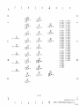
3.8
READING THE EPROM CONTENTS
The monitor firm\alare allot;.'S the user to read the contents of the
progra~ed
EPROM. A special dump program must be included with the user program in memory
to be transferred to the EPROM. Approximately 30 bytes of memory are requi red
for the dump program. This dump program may be relocated anywhere in the valid
EPROM space by changing the reset vector from 80 to the new start location.
Caution must be used in calculating branch offsets since this dump program
executes from EPROM and cannot be debugged by the monitor. The dump program
(listed in Figure 3-3) is written for an MCl468705G2 (reset vector at
IFFE-IFFF).
User I/O bit PC3 must not be held low by the user application circuitry during
reset.
After reset, all user I/O is available for applications (see
Figure 3-2).
The dump program for the MCl468705F2 is available with the F2 monitor program.
RESET
FETCH
RESET
VECTOR
YES
NO
USER
PROGRAt~
( RESET
ROUTINE)
READ
PROGRA~1
FIGURE 3-2.
!).Jffip
Progra.'1l Flo\"l
The procedure to perform the READ function is as follows.
NOTE
It is important that user circuitry connected to I/O connector Jl
does not pull down any of the user port lines during programming
or reading. Full CMOS levels are necessary on these lines.
a. Check switches S3 and S4 at the lower right of the EVM to assure that the
switches are in the OFF position.
b. On headers J15, J16, and J17, remove the jumpers from between pins 1 and
2 and install between pins 2 and 3 (see paragraph 2.3.9) •
c. Insert programmed r~1468705 into socket XU56 for the 28-pin device, or
socket XU57 for the 40-pin device.
d. Position switch S4 (+5VOLT) to the ON position and observe LED indicator
DS4 is lit.
e. Enter the command READ (see paragraph 3.6.16) •
f. The monitor displays the prompt (?) when the READ function is complete.
g. Position switch S4 to the OFF position.
h. Remove the programmed device.
additional devices.
Repeat the procedure from step c to read
i. When read task is completed, position the jumpers on headers J15, J16,
and J17 to pins 1 and 2.
3-27
Motorola M6805 X-Assembl.r
P
P
P
P
P
P
P
P
P
P
P
14
15
16
17
18
P
**
*
*
411.
.DUMPQ2
.SA 05/09/93 15: 19:06
**
*
*
*
*
*
*
DUMP
1468705G2
110 DEFINITIONS
*
*
*
*
DATA
PBO - PB7 ---)- EVM
*
*
RESET
RESET
<--- EVM
*
*
DATA REGUEST
EVM
PC3
<--*
*
DATA VALID
PDO
EVM
--->
*
*
*
*
******************************************************************************
P
P
A
A
0001
0005
0002
0003
0007
0080
OOFS
OOlF
0060
0061
0062
19 A
20 A
21 A
22 A
23 A
24 A
25 A
26 A
27
28
29
30
31
32
33
34
35
36
37
38
39
40
41
42
43
44
45
46
47
48
49
50
51
52
53
54
55
FIX
******************************************************************************
1 P
2 P
3
4
5
6
7
8
9
10
11
12
13
1. 10
A
the 1468705G2 ROM data From $80 - $8F4 .nd From
EVM, iF the DATA REGUEST bit (PC3) is held low
held high at res.t, the USER program is execut.d.
be used without this restriction.
This program dumps
$lFF5 - $lFFF to the
at reset.
IF PC3 is
After reset, PC3 can
DATA
DATADR
REQUEST
VALID
VALIDDR
RESET
ROMEND
VECTRS
FETCH
PAGE
BYTE
EGU
EGU
EGU
EQU
EQU
EQU
EGU
EGU
EQ\4
EGU
EGU
Oat. Bus (PORT B)
Data Bus direction register
Data Request (PORT C)
Valid Data (PORT D)
Valid Data direction r.gister
Reset Vector
LSB of the last ROM address to dumped
MSB of Vector addresses
Start of selF-modifying code
Address pointer MSB
Address pOinter LSB
SOl
SO:5
S02
S03
S07
S80
SF5
SIF
$60
FETCH+l
FETCH+2
P
P
******************************************************************************
P
P
P
**
*
*
*
**
*
FETCH
S0080
LOA
*
RTS
*
*
*
******************************************************************************
P
P
P
P
P
A
A
A
A
A
A
A
A
A
A
A
A
A
A
A
A
A
A
0080
0080 060238
Q383 A6C6
0085'8760
0087 3F61
0089 A680
00813 13762
0080 4C
008E 8763
0090
0092
0094
0096
READ
A6FF
13705
13707
AEFS
0098 1103
009A 0702FD
56 A 009D
START
~,DC
1
57 A 009F 8701
58 A aOAl 1003
LOOP
WAITl
SELF-MODIFYING
~ODE
AT RAM $60
ORG
I3RSET
RESET
3, REQUEST. USER
LOA
STA
CLR
LOA
STA
INCA
STA
#$C6
FETCH
PAGE
#$80
BYTE
LOA
STA
STA
LOX
#$FF
DATADR
VALIDDR
#ROMEND
ConFigure 'Data Bus and Valid Data ports
as outputs
BCLR
BRCLR
0, VALID
3, REGUEST,WAITl
FETCH
DATA
O,VALID
Send: Data invalid
Wait For Data Request
Q;:t n.xt bijtc
Send it
Send: Data valid
BSR
STA
BSET
FIGURE 3-3 ..
Execute user program?
No.
trans'er selF-modifying code to RAM
BYTE+1
Dump program Li.sting (Sheet 1 of 2)
3-28
Motorola M6805
59 A
60 A 00A3
61 A OOA5
62 A 00A7
63 A 00A9
64 A OOAB
65 A OOAE
66 A 0080
67 A 0082
68 A
69 A 00B4
70 A 00B6
71 A 00B9
72 A
73 A OOBB
74 A
75 A
76 A IFFE
77 A
78 A
X-Assemble~
1. 10
3C62
2700
B362
260B
076108
AE1F
BF61
2002
FIX
411.
. DUMPG2
BYTE
MSB
BYTE
WAIT2
3. PAGE. WAIT2
.SA 05/09/83 15: 19:06
INC
BEG
CPX
BNE
BRCLR
LDX
STX
BRA
~WECTRS
Inc~ement ~ddress pOinter
Roll over to MSB ?
No, end of progr~m ROM LSB ?
No. continue
End
program ROM ?
Yes. change address pOinter MSB
PAGE
WAIT2
~nd
0'
continue
3C61
0602FO
2000
MSB
WAIT2
INC
BRSET
BRA
PAGE
3.REGUEST.WAIT2
LOOP
Increment address pOinter MSB
Wait for: Qot dat~
Continue
20FE
USER
BRA
USER
User program starts here
IFFE
0080
VECTOR
ORG
FDB
$1FFE
RESET
Reset vector
END
START
0080
***** TOTAL ERRORS
***** TOTAL WARNINGS
0-0--
Motorola M680S X-Assembler
loc~tion
0
0
1. 10
FIX
.DUMPG2
411.
.SA 05/09/83 15: 19:06
SYMBOL TABLE LISTING
SYMBOL NAME
BYTE
DATA
DATAOR
FETCH
LOOP
MSB
PAGE
READ
REQUEST
RESET
SECT VALUE
A
A
A
A
A
A
A
A
A
A
0062
0001
0005
0060
0098
0084
0061
0083
0002
0080
SYMBOL NAME
ROMEND
START
USER
VALID
VALIDDR
VECTOR
VECTRS
WAITl
WAIT2
FIGURE 3-3.
SECT VALUE
A
A
A
A
A
OOFS
0080
OOBB
0003
0007
A
iF"FE
A
A
A
OOIF
009A
00B6
Dump Program Listing (Sheet 2 of 2)
3-29/3-30
CHAPTER 4
FUNcrIONAL DESCRIPTION
4 .. 1
INTRODUcrI rn
This chapter provides a block diagram description of the EVM module.
diagram is shown in Figure 4-1.
4.2
A block
BLOCK DIAGRAM DESCRIPTION
The EVM is designed to simulate an MC1468705 MCU with the resident MC146805G2.
Data transfer within the EVM is controlled by the monitor ROM firmware
controlled from an external R8-232C compatible user terminal. The contents ,of
the monitor ROM are not available to the user.
After system initialization, the EVM waits for a comnand line input from the
user terminal. When a proper command is entered, the operation continues in one
of tv.u basic IOOdes.
If the command causes execution of a user program, the
rooni tor mayor may not be reentered, depending on the desire of the user. For
the alternate case, the command is executed under control of the monitor, and
the system returns to a waiting condition after conunand completion.
During
command execution, additional user input may be required, depending on the
command function.
rrhe monitor requires five bytes of user stack for user register storage upon
monitor (re) entry. No limitation is placed on the user as to other uses of the
stack.
All user reg isters are in an unknown state on monitor power-up.
4.2.1
Decode and Map SWitch Logic
The EVM operates in either one of two maps (monitor map or user map) (see Figure
3-1). The monitor map contains 4K bytes of RAM/ROM, which includes a user stack
pointer, a monitor control register, monitor I/O, monitor RAM/stack, and the
roonitor ROM. The user map contains the user I/O ports, user RAM/stack, and user
pseudo ROM. A temporary map switch which allows modification of user memory,
and a permanent switch which allows execution of user programs are provided on
the EVM.
Temporary Map SWitch
The temporary map switch executes any three-byte instruction in the user map and
returns irrmediately to the monitor map. The opcode and operand are fetched from
the monitor map, maps are switched, and the instruction is executed in user
space. Maps are switched automatically back to the monitor map at the beginning
of the next load instruction register (LIR) from the processor.
4-1
The permanent map switch is initiated by conunand from the monitor, or by the
USER RESET switch. Return to the monitor occurs at a breakpoint, at the end of
a trace function in the monitor, or the ABORT switch.
The return from interrupt (RTI) opcode is fetched from the monitor map, maps are
switched, and the registers are fetched from the user stack. Execution proceeds
from the program counter (PC) fetched from the user stack.
When the USER RESET switch is pressed, the MCU and all user I/O are reset, maps
are immediately switched to the user map, and the reset vector is fetched from
the user map by the MCU. Breakpoints are ignored during this mode of execution.
Execution of user code continues until an SW! is decoded on the data bus during
an LIR, and either the breakpoint flip-flop is set or the ABORT switch is
pressed. '!be map is switched back to the monitor map after the registers are
saved on the user stack. An SW[ which occurs when no breakpoint is set -- and
when the ABORT swi tch is not be ing pressed -- does not cause a map swi tch. This
allows user SWI's to be executed in real time.
'!be ABORT switch, when pressed, forces an SWI on the data bus until the next
LIR.
'!be reg isters are saved on the user stack and maps swi tched to the
monitor. '!be ABORT switch has no effect on the monitor map.
When the USER RESET switch is pressed, the MCU and user I/O are reset into the
user map. When the ABORT switch is pressed while in the user map, the monitor
map is reenetered.
4.2.2 Monitor I/O
'!be monitor I/O consists of two serial R8-232C ports, a cassette port, and a
parallel printer port.
Terminal Port
'!be terminal port communicates with an RS-232C compatible terminal in character
mode. Baud rates are selectable through the use of a jumper on header J12. A
software transparent mode allows direct cOImlunications between the terminal and
the host.
H:>st Port
'!be host port provides downloading of 8-records from an RS-232C compatible host
computer (EXORciser or any modem). Baud rates are selectable through the use of
a jumper on J12.
Cassette Port
The cassette port provides a means of dumping and loading S-records to and from
'!be recording technique is unique to the EVM.
an audio cassette recorder.
4-2
Printer Port
The printer port interfaces with any standard Centronics type parallel printer.
Seven data lines, strobe, and acknowledge are the only signal lines supported.
When the printer port is activated, all information sent to the terminal is
echoed to the printer.
4.2.3
User Map Area
The user map area consists of the user RAM/stack and the user pseudo ROM.
User RAM!Stack
The user stack is resident in memory from OIO-07F. The stack pointer value is
displayed when trace and breakpoint functions are executed.
For detailed
information on the stacking order, see the specific device data sheet.
User Pseudo RCM
The user program space 080-FFF is RAM, which is write protected during user
program execution.
'Ibis feature requires all programs to be RCXV1able and
protects against program errors which would otherwise overwrite the program
space.
A jumper on header Jl8 provides selection of a 2K-byte user map for evaluating
the MC1468705. Vectors fetched from 7FS-7FF in the user program appear to the
resident MCU at IFFS-IFFF. 'Ibis is accomplished by shadowing the lower 2K map
into the upper 6K bytes during this option.
4.2.4
User I/O Ports
All user I/O ports (A, B, c, D) are available in the user map for evaluation.
All ports are reconstructed off chip except port C.
The on chip timer, AID, and interrupts are available to the user.
4.2.5
EPROM Programmer and Reader
The MCl468705 MCU devices have an internal boot programmer program. When the
appropriate voltages are applied externally and reset is lifted, the boot
program is entered by a vector. The program takes data from the EVM I/O ports
and transfers the data into the internal EPROM of the MCU device.
The contents of the programmed EPROM may be read by the EVM. A small program
can be added to the user code, which allows the contents of the EPRa-1 to be
downloaded to EVM memory.
4-3
ADDR
DATA
CNTL
CONTROLMCU
r- - -
----I
f
USER
I
: APPLICATION ~
L- _____ -I
MC146805G2
DECODE
&
MAP SWITCH LOG IC
TIMER
----
(USER)
(MONITOR)
a::
a::
c(
0
0
....c( ....-'
Z
0
a::
0
0
a::
0
a::
0
c(
0
2
a::
a::
f/)
;:)
;:)
UJ
Z Z
0
2
....c(c( ....-'Z
c(
.... .... ....
Z
0
0
0
0
W
fJ)
a::
W
fJ)
;:)
RAM
STACK
USER
PSEUDO
ROM
0
2
RAM
STACK
MONITOR
ROM
I
I
j-------,
USER
0....--
USER
I/O
PORTS
r- ----., -:
I TE RMINAL:
____ J
I
'--
-..
r
TERMINAL
RS-232C
PORT
BAUD
RATES
1
I
I EXTERNAL.
I
I
CLOCK
L_
I
4FO
l~
---..,
-
,
HOST
SOFTWA RE I
RS-232C
i DEVELOPMENT I
~
PORT
I ______
SYSTEM -J1 - - - -..L..-_ _ _
L
I
&
READER
CASSETTE
PORT
-----'
,.----- -1
OPTION AL
I
I
ON-CHIP EPROM
PROGRAMMER
CLOCK
- , ---,
....
--
rO;TI ONAL.
AU 010 •
I CAS
1_ -
:E~EJ
1
~
!1~. __P_R_I_N_T_ER_~~---~f O~~;N;:C-1
_
FIGURE 4-1.
_
PORT'"
EVM Module Block Diagram
4-4
I
iL _
APPLICATION
_ _ _ _ _ .JI
I
I
I
~-..-.
r-OP-:;:ION-;'~~
I
. , CENTRONICS
I
IL _PRINTER
_ _ _ _ _ JI
CHAPTER 5
SUPPORT INFORMATION
5.1 INTRODUCTION
This chapter provides the interconnect signals, parts list with parts location
illustration, and schematic diagram of the EVM Module.
5.2 INTERCONNECT SIGNALS
The EVM interconnects through cables wi th a terminal, a host computer, a
printer, and a cassette recorder. See paragraph 2.4.5 for cassette connectors
J6 and J7.
5.2.1 Terminal Port J3 Interconnect Signals
'Ibe signals at edge connector J3 on the EVM module are RS-232C compatible.
Table 5-1 lists each pin connection, signal mnemonic, and signal characteristic
for the connector.
TABLE 5-1.
PIN
NUMBER
,
Terminal Port J3 Interconnect Signals
SIGNAL
MNEMONIC
SIGNAL NAME AND DESCRIPTION
"I
.l.,~
3
TxD
Not used.
4
5
RxD
CTS
DSR
GND
16-20
SIGNAL GROUND - 'nlis line provides a common signal
ground connection to the RS-232C device.
Not used.
14
15
DATA SET READY - 'Ibis line is held high to be compatible
with terminals requiring this signal.
Not used.
12
13
CLEAR TO SEND - This line is held high to be compatible
with terminals requiring this signal.
Not used.
10
11
RECEIVE DATA - 'nlis line transfers data to an R8-232C
terminal device.
Not used.
6,7,8
9
TRANSMIT DATA - This line accepts input data from an
RS-232C terminal device.
DCD
DATA CARRIER DETECT - 'nlis line is held high to be
compatible with terminals requiring this signal.
Not used.
5-1
5.2.2
'l1h"",
.&..&.,,'-
Host Port J4 Interconnect Signals
~;,..,,..,.:.l~
1J"'~'.I.\.4....L.""
:.-1-
\.Aw
oA,..,o
'-""'~"'""
,..."',..,.,..,.0,...-1-",1'"
",v~.u.l.'-'"''-V'"
,.)1
u-z
"',..,.
""-1.1'&
-I-ho
'-".L'&'-"
~1M
~v,,-,
""",Alllo
"I'V",",\,A.,-
:'1"'0
\oAJ..'-
oc_,>"),>"
""''-''''
~.,JL.'-'
,..."'..... n:.-I-;hlo
"",,VIL"~""".""''',"-.
Table 5-2 lists each pin connection, signal mnemonic, and signal characteristic
for the connector.
TABLE 5-2.
. SIGNAL
MNEMONIC
PIN
NUMBER
3
TxD
4
RxD
7
RTS
RECEIVE DATA - This line accepts input data from an
RS-232C modem device.
REQUEST TO SEND - This output signal line requests
permission from the RS-232C device to send data.
Not
8
CTS
9
used.
CLEAR TO SEND - This input line grants permission to
send data (see paragraph 2.3.4).
Not used.
10,11,12
GND
SIGNAL GROUND - This line provides a coI11tlon signal
ground connection to the RS-232C device.
DATA TERMINAL READY - This output line is held high to
be compatible with devices requiring this signal.
14
5.2.3
used.
Not used.
6
16-20
TRANSMIT DATA - This line transfers data to an RS-232C
modem device.
Not
5
15
SIGNAL NAME AND DESCRIPTION
Not used.
1,2
13
Host Port J4 Interconnect Signals
DCD
DATA CARRIER DETECT - This input line indicates that the
carrier signal has been detected (see paragraph 2.3.4) •
Not used.
Printer Port J9 Interconnect Signals
The signals at connector J9 are Centronics type printer compatible. Table 5-3
lists each pin connection, signal mnerronic, and signal characteristic for the
connectors.
5-2
TABLE 5-3.
PIN
NUMBER
Printer Port J9 Interconnect Signals
SIGNAL
MNEMONIC
SIGNAL NAME AND DESCRIPTION
Not used.
1-24
25,26
GND
GROUND
27
PR7
PRINTER DATA line (bit 7) - One of seven output data
lines to the printer.
28
GND
ROUND.- PR7 signal return line.
29
PR6
PRINTER DATA line (bit 6) - Same as PR7, pin 27.
30
GND
GROUND - PR6 signal return line.
31
PRS
PRINTER DATA line (bit 5) - Same as PR7, pin 27.
32
GND
GROUND - PRS signal return line.
33
PR4
PRINTER DATA line (bit 4) - Same as PR7, pin 27.
34
GND
GROUND - PR4 signal return line.
35
PR3
PRINTER DATA line (bit 3) - Same as PR7, pin 27.
36
GND
GROUND - PRJ signal return
37
PR2
PRINTER DATA line (bit 2) - Same as PR7, pin 27.
38
GND
GROUND - PR2 signal return line.
39
PRl
PRINTER DATA line (bit 1) - Same as PR7, pin 27.
40
GND
GROUND - PRI
si~l1al
line~
return line.
Not used.
41,42
43
STB*
DATA STROBE - A low level output signal used to strobe
the data on PRI-PR7 into the printer.
44
GND
GROUND - Signal return line for STB*.
Not used.
45,46
47
ACK*
ACKNOWLEDGE
An activae
low level input signal
indicating acceptance of the data into the printer.
48
GND
GROUND - Signal return line for ACK*.
49-50
Not used.
5-3
5.3
PARTS LIST
Table 5-4 1 ists the components of the ~VM module.
'!he parts locations are
illustrated in Figure 5-1.
'Ibis parts list reflects the latest issue of
hardware at the time of printing.
TABLE 5-4.
REFERENCE
DESIGNATION
EVM Module Parts List
MOTOROLA
PART NUMBER
DESCRIPTION
a4-WB143BOl
printed wiring board
CR3,CR4
4aNW9607AOl
Rectifier, 1N4001
Cl,C15,C21
23NW961aA33
Capacitor, electrolytic, 22 uF @ 25 Vdc
C2-C14,C16-C20,
C22-C45,C47-C50
21SW992C025
Capacitor, fixed, ceramic, 01 uF @ 50 Vdc
C46
23NW961aA22
Capacitor, electrolytic, 50 uF @ 16 Vdc
C51
21SW992COIO
capacitor, fixed,
DSI-DS4
4aNW9612A24
Diode, light emitting, red
J1
2aNW9a02C29
Header, double row post, 4 pin
J2,J5,Ja,JIO,
J13,Jl5-Jla
2aNW9a02D04
Header, single row post, 3 pin
J6,J7
09NW9a03A27
Jack, phone, subminiature, 2 contact
Jll,J12
2aNW9a02B34
Header, double row post, 16 pin
J14
2aNW9a02DOl
Header, double row post, 2 pin
PI
31NW9509A27
Terminal block, 7 position, screw contact
Ql,Q3-Q6
4aNW9611AOl
Transistor, 2N4403
Q2
4aNW9610AOl
Transistor, 2N4401
Rl,R13,R14,
Rl5,Rl7
06SW-124A37
Resistor, fixed, film, 330 ohm, 5%, 1/4 W
R2
51NW9626A92
Resistor network, 5/39k ohm
R3,RB
06SW-124A89
Resistor, fixed, film, 47k ohm, 5%, 1/4 W
R4
06SW-124A97
Resistor, fixed, film, lOOk ohm, 5%, 1/4 W
R5
06SW-124A81
Resistor, fixed, film, 22k ohm, 5%, 1/4 W
R6 ,R25 ,R37 ,R39
06SW-124A65
Resistor, fixed, film, 4.7k ohm, 5%, 1/4 W
5-4
cer~~ic,
470 pF @ 50 Vdc
TABLE S-4.
EVM Module Parts List (cont'd)
REFERENCE
DE8IGNATION
MOTOROLA
PART NUMBER
R7,R16
SlNW9626A46
Resistor network, S/4.7k ohm
R9,R18,R19,
R33,R38
06SW-124A41
Resistor, fixed, fibn, 470 ohm, S%, 1/4 W
Rl1
SlNW9626A37
Resistor network, 9/10k ohm
R12
SlNW9626A93
Resistor network, 7/470 ohm
R20
06SW-124A32
Resistor, fixErl , fibn, 200 ohm, S%, 1/4 W
R21
06SW-124A69
Resistor, fixErl, film, 6.8k ohm, S%,_ 1/4 W
R23
06SW-124A77
Resistor, fixed, film, lSk ohm, S%, 1/4 W
R24,R32
068W-124A49
Resistor, fixErl, . film, 1.0k ohm,
S~
R26
06SW-124A60
Resistor, fixErl, film, 3.0k ohm,
S~
R27
068W-124A71
Resistor, fixErl, film, 8.2k ohm,
5~
R28
068W-124A44
Resistor, fixErl , film, 620 ohm,
S~
R29
06SW-124A42
Resistor, fixErl, film, S10 ohm,
S~
R30
068W-124A20
Resistor, fixErl, film, 62 ohm, S%, 1/4 W
R31
06SW-124A7S
Resistor, fixErl , film, 12k ohm, S%, 1/4 W
81,82,8S
40NW9801AS4
SWi tch, pushbutton, 8POT
83,84
40NW980lB33
SWitch, slide, DPDT
Ul,U14,
U19,U46
SlNW961SC22
I.C. 8N74LS08N
U2,U4
SlNW961SB94
I.C. MC68S0P
U3
SlNW961SB30
I.C. MC1489AL
US,US2
SlNW961SE88
I.C. 8N74LSI0N
U6,U44,US3
SlNW961SE9l
I.C. 8N74LSOON
U7
SlNW961SE72
I.C. MC14S83CP
U8,UI0,U32
SlNW961SF02
I.C. 74LS244N
U9
SlNW961SB27
I.C. MC6821P
DESCRIPTION
S-S
0, 1/4 W
0, 1/4 W
0, 1/4 W
0, 1/4 W
0, 1/4 W
T~.BLE
5-4.
BlM Module Parts List (cont'd)
REFERENCE
DESIGNATION
MOTOROLA
PART NUMBER
UII,USI
SINWJ6ISE89
I.C. SN74LS260N
UI2,U31,U48
SINWJ6ISF76
I.C. SN74LSIIN
Ul3
SINWJ6ISH50
I.C. SC82027P
UIS
SlNWJ6lSB29
I.C. MCl488L
U16,U36
SlNWJ6lSC20
I.C. SN74LS02N
UI7,U40,U43
SlNWJ6lSC21
I.C. SN74LS04N
Ul8
SlNWJ6lSCS6
I.C. 74S08N
U20
SINWJ6ISE99
I.C. SN74LS374N
U21
SINWJ6ISE96
I.C. SN74LS24SN
U22
SINW9615G98
I.C. SC89146P
T
I" "l
OJ&...J
(See note)
I.C. programmed
U24
SINWJ6ISE80
I.C. MCM68BIOP
U25,U26
(See note)
I.C. programmed
U27,U28
SlNWJ6lSHS9
I.C. HM5116P-4
U29
SlNVB6lSE77
I.C. SN74LS27N
U30,U49
SlNWJ6lSF38
I.C. SN74LS393N
U33
51NWJ61SM97
I.C. MC74HC374N
U34,U3S,U41
SlNVB6lSC24
I. C. SN74LS32N
U37,U42,
U4S,U47
SINW96ISC2S
I.C. SN74LS74N
U38,U39
SINW96ISH51
I.C. SYP6S22
USO
SIN\\96ISBSI
I.C. MCl4024BCP
US4
SINW96ISM96
I.C. ftC74HCU04N
USS
SINW96ISE93
I.C. SN74LSl4N
VRl
48NW9608Al4
Diode, zener, INS244B
VR2
48NW9608A06
Diode, zener, IN963B
DESCRIPTION
5-6
TABLE 5-4.
EVM Module Parts List (cont'd)
REFERENCE
DES I GNAT I 00
MOTOROLA
PARI' NUMBER
Yl
48NW9606A32
Crystal, 4.0 MHz
09NW98llAl5
Socket, OIL, 24 pin (use at U24-U28)
09NW98llA39
Socket, OIL, 40 pin (use at XU57)
09NW98llA2l
Socket, OIL, 28 pin (use at U23)
09NW9811A38
Socket, OIL, 28 pin (used at XU56)
09NW9811A22
Socket, OIL, 40 pin (use at U13, U38, U39)
29NW9805B17
Jumper, shorting (use at JI, J2, J5, J8,
JIO, JII, J12, J13, JI5-JI8)
DESCRIPTION
NarE: When ordering, use number labeled on part.
5.4
SCHEMATIC DIAGRAM
Figure 5-2 illustrates the schematic diagram for the EVM module.
5-7
EI
£4
- - - . _ _ _ _ _ _ _ _ _ _ _ _ _ _ _ _ _ _ _1
FIGURE 5-1.
EVM Module Parts Location
6
7
5
NOTES:
I. FOR REFERENCE DRAWINGS REFER TO
BILLCS) OF MATERIAL 01-W314JB01
2. UNLESS OTHERWISE SPECIFIED:
ALL RESISTORS ARE IN OHMS. ± 5PCT.
1/4 WATT.
ALL CAPACITORS ARE IN UFo
ALL VOLTAGES ARE DC.
3. INTERRUPTED LINES CODED WITH THE
SAME LETTER OR LETTER COMBINATIONS
ARE ELECTRICALLY CONNECTED.
&DEVICE TYPE NUMBER IS FOR REFERENCE
ONL Y. THE NUMBER VARIES WITH THE
MANUFACTURER
5. SPECIAL SYMBOL USAGE:
DENOTES - ACTIVE LOW SIGNAL.
S. INTERPRET DIAGRAM IN ACCORDANCE
WITH AMERICAN NATIONAL STANDARDS
INSTITUTE SPECIFICATIONS, CURRENT
REVISION.
PART TYPES ARE ABBREVIATED IN
THE FIELD OF THE DRAWING, FOR
FULL PART TYPE. REFER TO TABLE I.
B.
I INDICA TES EQUIPMENT MARKING.
9. CODE FOR SHEET TO SHEET REFERENCES
A§
IS AS FOLLOWS:
SHEET
~ZONE
D
4
3
~
C2
C3
CS
D
15V
C1 IC8 IC9 IClll IC11 ICI2' ICI3"ICI4 IC16 IC4
~1 ~I ~I ~I ~1 ~1 ~1 ~I ~I ~1 ~I ~1 ~1
*
&.
J
c
TABLE 1
Pl-~
>
+1~V
..
J.1.l
~4l..S1fld
U2
U3
MC6~0
JJA
l'-5
llS
U7
U8
U9
UI0
UJI
UI2
U13
·U14
UI5
U16
U17
U18
U19
U20
U21
U22
U23
U24
U25
U26
U27
U28
U29
B
TYPE~
MC1489A
74L~
~
74J.....Sia
~
MCI458~
~
74LS244
10
MC6~1
1
74LS~44
10
~?SCIJ
~
141
741.SJI
MC146S05G2
74LS0S
MCL4Jla
74L.S02
74LS04
14S1I_8
741.S"e
74l.S314
74L.S245
74LS373
82S103
......
MCM2116
MCM2716
HM6116
HM6116
74L.S27
UJI
U32
74LSJI
74LS244
74HC374
74LSJ2
74LS32
U34
14
12
14
12
14
14
16
20
20
20
14
14
40
14
1
74LS~93
~
7
I
7
M~
J.Lla
~
+5V
P)-5
)
L
2.S
I
I
7
I
~
7
10
10
HI)
14
I
12
12
12
12
7
7
7
11
10
7
7
+12V
C
25V
&
GND
112V
l}22 ~I
-12V
leI
REF
DES
~
+ IC21 ICls
~
12V
~
18V
IC17
lj22 ~I
+
-:-12V
PI-7
>
5V
-I~V
IC45
1
T·
\l
'
~
P)1-
&
TABLE I.CONToD
----
14
14
14
14
14
29
29
29
28
24
24
24
24
24
14
14
14
20
20
14
14
1
&
REF
DES
TYPE
U36
U.:U
U38
1~LSI4A
U3~
U4J!
U41
U42
U43
U44
U45
U46
U47
U48
U49
U5'
U51
U52
U53
U54
U55
XU56
XU51
74LSGJ2
SYP6522
SYP6522
741LSGJ4
74LS32
74LS74A
74LSGJ4
74LSIIJ9
74l.S74A
~
74LSIIJ8
74L.S74A
74LSII
74LS393
MC14024
74LS260
74LSI0
74LSII
741-1CUIIJ4
141.514
L~
;1\1=.
(~l
;1\1=.
-
J
)
GND
+5V
7
7
1
I
7
7
7
7
7
7
7
7
7
7
7
7
7
7
7
7
14
20
14
14
20
211
14
14
14
14
14
14
14
14
14
14
14
14
14
14
14
14
1+ 5VPR
YI
XU57
XUI THRU
XU55
VR2
U55
B
S~
R39
R10,R15,R22 •.
R34.R35,R36
Q5
E4
PI
DS4
J 18
CR4
CRI,CR2
CS0
HIGHEST
NOT USED
NUMBER
USED
REFERENCE DESIGNA TIONS
28
41
A
63DW3143B REV
7
6
5
t
B SH 1 OF 7+
<:III7Rr:-1
FIGURE 5-2.
A
EVM Module Schematic Diagram (Sheet 1 of 7)
5-9/5-10
7
6
D
NCPNCP4 U518
NC
NC
NC
NC
10
1
I
-.~
R2E
39K
9
I
~g 3Ji
-12V~NC
~g =Ai
C
R12G
470
+12V~NC
NC
NC
NC
RI6C
4700
+5~NC
NC
-m
1
NC
U31C
LSI1
)-L-
NC
U12A
LSI1
)1L-
+5~NC
NC
NC
NC
NC
~g =i1
NC
NC
RI6B
+5 ~
1.3
NC
\lC
NC
10
1
NC
~
NC
NC -
U6B
LS00
NC
U168
NC
NC
~
NC
U6C
LS00
NC
NC~
NC 1
NC
LS60
NC
NC
NC
bu-1
NC
U31A
NC
NC~
NC
12 NC
NC
NC~NC
'A~ NC
J3-1
J3-2
J3-4
J3-6
J3-7
J3-8
J3-1~
J3-1,
J3-14
J3-16
J3-17
J~-18
J3-19
J~-~'2
J4-1
~4-2
J4-4
J4-6
J4-~
J4-10
~4-11
J4-12
J1-16
J4-17
J4-1§
J4-1~
~4-2~
(
(
(
(
(
(
)
)
)
)
)
)
)
)
)
)
)
)
)
)
)
)
)
)
)
)
)
)
NC
NC
NC
NC
NC
NC
NC
NC
NC
NC
NC
NC
NC
NC
NC
NC
NC
NC
NC
NC
NC
NC
NC
NC
NC
NC
NC
NC
NC
NC
J9-1
)
J9-2 )
J9-3 )
J9-4 )
J9-5 -7
J9-6 )
J9-7 )
J9-8 )
J9-9 )
J9-10 )
J9-11
I
J9-12 ")
J9-13 )
J9-14 )
J9-15 )
J9-16 )
J9-17 )
J9-18 )
~9-19
J9-,0
J9-21
J9-22
J9-23
J9-Z4
JQ-41
J9-42
J9-45
J9-46
J9-49
J9-5'2
C
)
)
)
)
)
)
"j
)
)
)
)
)
)
)
)
)
)
NC
U52C
U53A
LS00
NC _ 1
NC
NC
NC
NC
NC
NC
NC
NC
NC
NC
NC
NC
NC
NC
NC
NC
NC
gLS32
.' .. '
Jl-17
Jl-18
Jl-19
Jl-,2
JI-23
JI-24
NC
U35C
NC
NC
NC
NC
NC
NC
NC
NC
NC
NC
NC
NC
NC
NC
NC
NC
U6D
U53C
LS00
B
~
I
UI6C
NC
II"',.,,""
VL~'"
NCV
NC
NC
NC~NC
LSIl
NC~
NC
U36C
UI8
LS08
NC=1LY- NC
NC
U3i8
)-L-
NC
=i[}-L NC
4
U12C
LSll
)-L-
3
0
UIA
LS08
U29B
R16A
4700
NCV-
4
U52A
Ul1A
NC
NC I
NC I
NC -
..
5
alSte)
NCI!L)LNC
8
NC
HC
NC~
NC
NC
B
U348
LS.32
NC~NC
NC
NOT USED
A
63DW31438 REV
7
6
5
t
FIGURE 5-2.
8 SH
2 OF
A
EVM fwt>du1e Schematic Diagram (Sheet 2 of 7)
5-11/5-12
7
6
4
5
3
o
o
+SVPR
+SVPR
R39
4700
6C3
6C3
6D3
4B3
6C3
6C3
C
UPD0
..
'PROGl
UPD)
..
'PROGl
UPB0-UP83
"-
, 8
"-
UPA0-UPA7
~
-
J)~
L)"
R37
4700
R25
4700
RESET*
3·2~)~-----=~~~------~------------------------------------~
J)!.
~ 3·2~1~--~~~~~~----~~-----------------------------------+--------------------------~~
"'.l.
VALID DATA*
'4
PRCLK
UPD3
~
+SVPR
,4
ADDRH
CLOCK
ADDR CG2)
,
VALID ADDR
,
8
XU57
(MCI468705G~)?A
, 3
"i"U;.:P-,:,A~0_---:I=-=--t PA 0
UP Al
I
PAl
UPA2
E
1"'.~llJP:-O:A~J=----~E PA 2
TSC ( F 2 ) ! '
6C3 UPD2
.DA T A ( ADDRL F 2 1 , B
UPC0-UPC2
.'
...
8
4D7 ~~~~--.-~----~~------------------~~~~~~~~~~--~----------~,,-~----------~
,
1"'.~lJP~,A~4~-~7~PA3
", '~;': '~-9A ~ ___{lIf-I~~i
XU56
87
I
__
0SF21-)-=-__
UP81
2) PB0
PA0
UPCl
I~UP:';B::-:2:---~2:-;;'0~PBI
PAl
UPC2.
'-='-~----'1~9'-1PB2
PA 2
UPC;}
18 PB;}
PA3 10
UPC4
r--4----:1~7~PB4
PA4 II
UPC5~
16 PBS
PAS 12
UPC6
::-:-::;:o:--t------+-+-----:1-=-5'-f~~~
~ ~ ~ 13
UP C7
~UP~8~0<-- ~2~2('-fMCI46
rr=--------'--------'VV\,-----+-----t----'-----L------::...:....:..---"'~~---_+_t_~---''''''_il"' t:J (
PC0 ~
PClm=27
6
PC2
PC3~24~~~
~girit-
~lJ:.,:IPC~0¥+-~_+--_"'U~P~'A~7====1~142~ ~:!
13
14
15
16
17
18
19
1
I"' 1-\ (
<Hi- PCI
PDI 30
UPBI
PD2r=3~1-------:U~P:-:B""'2"1
~327-------'U=-P~B~3" I
PB3
PB4
PB5
PBS
PB?
2
IRO.......L..
TIMER-ll...4
OSCI.4
VPP OSC2.i NC
~79
+5VPR
..J
NC~
NC
;~~~:2~9~1~=:_---.;U¥.;P::.!;B~0"1
PB)
PB2
PD3 3"
1
PD4~ NC
PDS~
~~~ DOL:
, ." ,.
~_+~~2~6~PC0 RE~.~l~--~--~-L---------_+~~~~
L---+---+-+~~~4'-fPC2
NCr2L PC3
c
I
I I
rfcfET VPP~
TIMER/BOOT
OSC)
OSC2
~
'--'-'-..::....::..---~
'\§9
VPP
I PROGRAM I
R30
62
~
zn:'
R23
15K
-12V
~'
R24
IK
03
2N4403
I
q
IPROGRAM
I
[QIT]
[Q:[J
1
S3
2
I
I
I
S4
~.
18V
JI.
R28
• 620
: t 3§
I
I
I
2
M
~
I
5
VR2
IN963
12V
t :36
t
4
+5VPR
5
7
DS2
IVERIFIED I
5VPR
_ C50
CR4
IN4001
....
..
RI8
470
+)
~
15V 1+5V
~
I
I
@ill
SV
[QEJ
lC44
lC48
~1
~1
R;}8
470
\
'~ ~DS4
B
R'
®"/
\,!Y
DS3
EPROM PROGRAMMER
63DW31438 REV 8
7
6
I
5
t
FIGURE 5-2.
SH 3 OF 7
A
EVM frbdu1e Schematic Diagram (Sheet 3 of 7)
5-13/5-14
~
5
6
I
4
I
I
I
I
I
3
I
.5V
D~-[)7
RIIC
RlIF
RIIJ
RllH
R110
RllE
RllA
UIJ
RIIB
UJ3
HCJ74
..
MC146805(;2
3 10K 4 11K 7 10K 10 10K 9 11K 6 11K 5 11K 2 11K
r-~~~------~~~~--------------------------------------------~2~8~PC0
00 IN~II~--4----+----~--~----~--~r---~----~--~~Q
0~;~_~0!0
r-~~~------~~~.---------------------------------------------~2~7~PCl
DI IN~~I~~------~----4---~----4-----~--~----~--~~
~.~
------------------------------------------~2~6~PC2
2 IN 9
Q
0~7~-~D'2~1
>--~~~------~~~~--------------------------------------------~2~5~
0
8
Q
0 8
03
~~~~------_1~~~--------------------------------------------~2~4~PC3
03 IN 7
1 Q
0~13~~0~4~1
r-~~~------__i~~f__-----------------------------------------~2~3~PC4
04 IN, 6
1 Q
D~14~-.!f-CD=":5
~~~~------~~~~--------------------------------------------~2~!2yPC5
05 IN 5
tS Q
0~17~~0~6
L-~~L_
_ _ _ _ _ _~~~----------------------------------------------~2~I~PC6
06 IN 4
19 Q
0~~18~-~CD~'7~1
~
~ PC7
07 IN
Q
0
OE
C.....
U34C
U54C
NC 4 P05 A5/00 OUT 12 MX5
,I't'
A6/01 OUT 13 MX6
9 LS32
HCU04
A7/02 OUT 11 45 -MX-7'
~~-------l4----~-~-?-:-A~~~0a---~J~e---+-5-V----~5~ >~6____~
A8/03 OUT 16 MX8
'- 8
17
"
3
D0.
I
AII/06 OUT 18 MXII MX5 17
.01
~
·R7C
A12/07 OUT 19 MXl2' MX6 15
02
7
33 MA0 MX7 I:r
4700
03
9
~~I 3-2 MAf MX8 11
4
~~ ••. ~ ...
,,,
~__________________~T~~
~
MX9
IL
D4
A2 31 MA2 MXI0 I
.2 R.E.SET
14
05
A3 30 MA3 MXlI
.-----~lRQ
16
06
A4 -29 MA4 MXI2
8
18
D7
JI-20
~~~3
~~~~~
/
OEI La
.--+-~3~i9_l~~~{ 02
RI W ~
I
OE2
\..8
YI
NC ~~O-=-S-=-C.=.2____--=L=lRI=-~t)-+--.
4MHZ
+ ~V
"
lliTI~
0
,12
A4
I
3
RJ4
RJ3
14MHZ 1 ~
A5
R7E
"1500
1500
A6
v
( 4700 UI8C
'\4
A7
6
U40A
U400
U408
U548
10,508
A
[
lS04
A0
LS04
3HCU04
A~
91
8
MA0
-4)42
3
4
9
a
Al
/
~
A.
Ul4C
J LS08
Ui88
AI.
I
I
UISD
91
B
MAl
1I I
5 S08
I
LS02
5A3~U~/M~--------~----------~~
6
U140
~
-~.13
13l:.!~8
UI8A
A2
USA
121
'\ 11
MA2
1 S08 3
I ... LSJ0
583 08/0F*
~--~2~J
~-----------------+~~--~
U4SB
2':1
583 02*
13.J
583 06*
5
ill 8
U55C
U55B
AJ
4!
'\ 6
MA3
507
6C7
D
ljll
~~~g~ g~~
MMX~~'
L~~~4
-
C>
LO
"70"
10,.,
r
c
J14~i
I
IJ'3
,
r
I
I
~
+
~
)U-
I
I
USER
RESET
IIIII
I
RI7
330
I~I
U43E
LS04, ~
.I~
~
I I
1707
D7
607
P1-I2* W
rJ~12~__~________~_+------------------------------------------------------~-----L~
PH2 ~A7
,.
C7
UI7A
UJ78
LS04
LSI4
2
4
LlR ~87
i
:l
B7
LlR* 5C7
U4JD
U438
LS04
LSI4
~87
RW 5C7
9
a
:5
4
U4JF
,~LS04
I~
-
I
B
i
-
rMASTERj
RESET
I
-
+ V
R31
12K
~S5
NC~~:5
RW*
REG
OSC
RST*
PAR*
~07
r
LSI4
13~
B
C7,5C7
687
707
507
SA7
PRClK
JC7
U55F
.12
POR* 5C7
787
lC46
51
A
c
A0-A11 SA3
6C7
707
~i6V
5
t
63DW31438
FIGURE 5-2.
REV
B SH
EVM M:>du1e Schematic Diagram (Sheet 4 of 7)
4
OF
A
5-15/5-16
7
6
5
4
3
+
483 RST*
-
483 PH2*
D
U3S8
_~;:~
I~1~L..~z.....;r__----__t_,
,8
403 De THRU D7
+~V
"
_.
11
"UI
f
~~01
R160
5 471"
14
LL
3~~
U54A
1
~2.4
lln
~
____
U45A
LS74A
0 PR
21 \. .J--+-3~CK
.
-V~----...Io4'i
1
U38A
LS393
CK g~ ~NC
a~"l 12lli~
a~ ~
CLR
C~R
U/M* 6C7
783
U350
12~2
aC~Nc
~
aO~NC
>-,,"1.!.......-1_--.J12
D
U17E
LS84
~
-
4C~607llHIL-------~----~--_r_;--_+--------------~---,--~~----~--------------------~------+-----~~
I
483 POR*
1
6
U118
4
~
U6A
LSII
~'5~...L!I~~t:$--L""""'S260
2
~
+<
~
U51A
LS261
U42A
S74A
2 0 PR a 5
i'.~~-+-~~UI-:8 r-~).:>"'----~------4-----------:1~~/ ~
D7
J
~01
LS!!
41
D0
I~
U378
LS74A
51
~>CK Q~
rLc
T
~.0~3~--------+_----~1~20 PRa~1-9---4--~~ll~LS02
c
.....u..~CK a~NC
~
CLR
)!-
101
~
U360
10
U44A
U44C
I 2TI LS00
'-):>3~~--~9"f"'"L-S0,0
4
Pi
U4SC
II~8
U44D
I
13
9
1
J
)0."8~+-+-+-
c
___
"'"-"
____~F1E:,/F
~------t_----4----------~i---------~-~----------+4-------~------------~-L-----------+--~-----.----
607
ABT
683 LIR*
483RRWW~------~--------t---------------t---------~--------~-----------}----~----------~~---------+----------------------------~
483==~------~--------~--------------~--.---------------------------~----~----------~
483 RW*
..
I
(
U43A
LSI4
~A!.LJI1~__~J""" 2
i
I I I
UI7C
LS84
o:;
s
AI
I ",.c.:..----~
I
483 PH2
3
U528
LSII
483-LI~IR~------~~----~~--~5~"
41
~~,S~______~____~--------------------------~
01
02
03
06
5
6
7
8
4
5
B 6
9
8 7
06
7
7
07~~~~----~
07~~~1~----~
B
II
~--~~----~A'
2
s~S
.1
AI
~2
~--~3~----~A2
+5V
UI48
~
~RISE
47'"
6
7 A5
IS
6
AS
~--~4~----~A3
~--~.5~----~A4
3
14
~--~7~----~A6
6
7
--'
L~
,..-rn
""""'""qS
.......,
4J
)I>X----+----I----I-~~CS2
~
tTI"-~
,5
~--~A~6~----~A5
i8
.9
II
R/W
II
'-'""",,C..;;..S5~-.!
II.---I~..:::-~~~~~~---.----.II
l
~e
U23
01~~--:!~12-------t
02~~~~3----~
03~~~~4----~
04~~~~5----~
OS~~~~6----~
4
04
05
~
08~r-~~11----~
00~~r--~~----~
"3 A7
22 A8
19 ~r.
+5v-2LvPP
NC
~
, 4
82S103
10
. -__~--------~0~12~·* 4C7
L...-..--I---411
S
7
A.
'----~-I12
}·::1,.,--1--~13
1..I'9-H::,,:-------:i!-~14
P-'::J~---~15
~~:.------~I6
AI
A2
A3
A4
AS
AS
7
7 17
~6 IS
19
.,I;U;'
5:.__----!!t.IIi:
~~11 0
A6
Ir
.4
III
'4
1P.'3~-~~3HI12
2
~ 113
I
1 114
.e
~e 115
F0 I~
FI
I
F2
F3
I
1
F4 1
_"0117* 6A 7
08/1F* 707
06* 4C7
4C7
IIB*
*
607
SII7FI-* 6C7
~A 607
FS~~--~------------------~~ 687
FS
F7
OE 19
LO 783
,8
RD" _
807 607
"
21
~
~~~
______+_------~~-----------------L------------~--------------------.-L----~~------~WUMrM
, 7
, 12
" 12
-..
AI _ All
A
" . "
7
6
"
5
t
FIGURE 5-2.
B
11117
F5~~--4-r------~------~1~1~~/7~'F~I*
;
~nt:
IS
AI* 687
707
'- 2
U26
MCM2716
U24
MCM68811 2
I
800!FFF* 6C7
I II
V-
63DW31438 REV
707
4C7
6A7
707
4C3
B SH 5 OF
71
A
EVM M:>dule Schematic Diagram (Sheet 5 of 7)
5-17/5-18
7
6
5
,8
607 OBe-OB?
P12*
483 WI7F*
583
8117FF*
583~
H~~~----------------------'
D
1.4;
5C7
02
~
SC3 F/F
U37 A
LS74A
U340
"2
LS
~
12J
)11
483 POR*
5C3 800/FFF*.,
C~R
U A
14
2L~I8
~
I
L
U C
41
U410
I'ft LS32
lJ. LS32
~19"- - - J>&....-8--,
J:)Jlu..II-+-I--a
9.J
~J
-ud
~
~~j;
V
U41A
~D-J_ _ _ _-+-......l-aLS32 3
n
5
,e
~:~~
~.-~A0
1.P.'=-21-~Al
~
3
~~_---L<I
A2
1h',74~--lA 3
;"A~S-~A 4
r:A~S-~AS
.P.:-~A6
UIC
9~8
2
583 1017FF* _
.~~
11J
-
l
(OI
8
rMAEl
c
CiK]
~
503 U/M*
~
_
4CI A0-AU'
,11
403 00-07_
483 RW*
"
A'
I ~ Ale
vAle
,
21
lJ
i'
D
L..:~r_S-~OE;::.J
---2L
~
28
118
dt :~~
OE
18
~
28
g:4:±:~g
UPAIJ-UPA7 3C7
'-t---t----~
1
3 J8
I R78
2
• 47fl
U3S8
C~~~1_____3~____-+______________~4~LS32 6
5]
D-"-------+----------I------~
, 2
up, 3 3C7
UP[ '2 3C7
UP)!
UPJl0 3C7
,8
,8
, 8
, 8
r"Ile.
UJ.0
LS244
,,~
"".A~,"-~'~o
1'·~A,~I-~t.O
I~A~2--_r~0
I ",?-~3-~--l 0
! ",?-'+
4s --:!I~43~ 0
I "'?--:-s---+:!7~ 0
"="=7,-----+-:i:~ 0
~_~IB~o
;21
3
S
6
7
+sv---J,-
U2f
LS374
,-lL~cP
OE!P"-j'
'~
a~----=
I,~e.
Q
a
Q
21
,2
r"-
.01
.01
18
7
02
6
L~~!5
Nc?J-IRQ
B 0 ~1~0+_4--++_+_+____:.)~·0"
E DI.
I
3: 01
B )2,
2
3 02
8 3
:3
3 03
~.
.8;~
i~ 04
B 6 .B06
2"7 05
B ,"7 .807
06
.l
3
3
IS
'6"
16
6
1
17.
Q~~~~
Q
Q
Q
!~6r--~
7
E~
L.-(}-J
X
..... E...c OE
6
26
~'-------~,~L'~~~--~~+-~~07
XlYf-
4-
UI9B
OE2~
Lse8
4J,-.---..,
r--+------....
6
I
r-t---------L!;l---/
II
f7
U39
SY6522
"
I I
::~'~4S~-.::~~~I~.y~ B A
2
c
r--.
,2
"
..
I ....
n
23 ffi
23 A7
A7':7-9-':2!'f2""1~:
U3SA
~2
3
U28
U38
_4-_....lU
""'IP...B'l&ill·..:.llf.IU 3C7
HM6116P 9
SY6522
Ol~~=--~-"::.0::=9
01 Ie
B Ie.
NC2.L IRQ
CA1J:NC
' 4
fiiO]
01 II
J
0HI)f-----,J~~irl'~8¥1I~-----~3H?_iOI
CA2~! NC
'
02 3
02 3
B 3 B il
3 01
PAe~2;--~U7::p~Be.+----~J+-I-~9:,,--<
03 4 :
03 4 4 . .8 12
02
P A1........:.:3~--;-:;U""'P;:8:q.t----~J+_I-_=_H!I'__'_<>
04 5
B
04 5
B :3
t 03
PA 21-----'4;------;:::U,;P~82;o:.t_----~J+_l-~I,;._1__<>
05 .~
8
05 ,~
56 .8 14
04
PA3t--'!5~--;,,;U~Pi!f'83,!,,-----~J,;-I'-~1;-2--<>
06 ~.
06 10
8 15
8
6
UPB4
JI-13
>
07 A ~7
8
07 7
7 .B 6
7 OS
~~;~7'--~U"=IP~B5=-------=:JJ~--'-1::;-4--<>
A
AI
..B 7
6 g~
PA6~8~----;:::U:.:.P~86~----~J+-I-~1::f-5--<>
A2
A1
PA 7~9~~U~IP.to:.B·7.!------~J..L..I-..J..IS~_<>
A3
A2
'A
P8el-.J:lll"~-..::.rLU+=PA~\e~----~J+---!:I,---<'"
A4
A3
3~ RESET PB11-:'-::1I=----:-=:U~P-f=!A:&+r ____~J+--~·2:---_<>
AS
A4
22
1-7.112~_-7.lU-l;;"IP,=",'2=rt-·_ _ _ _ _~J+---";3:--_<>
A6
AS
25 R/W
P82 13
UP 3
J -4
>
1'?:----~A6
2'
E
P83~4;---.':'Ui:o'P~4~----~J+---.:5;---<>
~~
23 A7
~~~~~=----=-=lU-l:::"IP':>'S:ri------=:J....--=s'---<>
A9
~ A8
Ae 38 RSI
P86~7=----?;l~=I~£?:~~----~J+---:7,---<>
AU'
l.a ~~fA2 37 RSI
P871--W'----":O=:.:.....c...:....-f-----~J..L..-..:.8~-<>
U27
HM61\6P
2 Ir---'oP"--R~ 5
J)~
!O
Q
C2
3 i. CK Q~ NC"
r3~"""""'<l
r
4
CAI1:NC
CA2-= NC
11101
PAI~2;----+--l-+-'---:U:':\:P~I~"--"'J-!---:::3~3--<
PAI~3'----+--l-'----:u~p~n-~J-!---:::3'-::!-4-<>
PA21-----'4'---+--4-_ _-:U~P:_!:'-=--2~J_!_-_:::3~S__<>
PA3+---':i~;--~-----;~=:-;,~~'D~"?-~j,;-,:-:;5;-;;;~--<;
PA4 7
UPOS
Jl-38 >
PA5~8------:U<:;:;'P~10-:-16--":J~I--=3~9-<>
PA6~9'-----------:U~P:-!:10~7--"'J-!-I-~.4~I-<>
PA 7~'--------"'-'-..&.J...-..><.L.--L.X__<
P8f-1:8 NC
...
34
RESET
P81
~l1j
NC
22 R/W
P82 2 NC
t - + _....2
....
~5~ E
P83 3 NC
24 "~1
P84 4 NC
1-+-+-+-+--t1--:--:~23H ~
PB5 -J.~ NC
AI 38 ~~~
P86 =t~ NC
.A2 37 RSI
PB7 -I.' NC
, 2
'-
I
f'~~5 giiP:= ~g
483~
RE:~IG__~------_+------------------~------__l__+--------I__----------~--__.
USB
B
5B3
~~~L--I-__________~
eA
{:>J-2-
UIO
12~
S2
ri31--.JU---
lI.
483~~------~------------~~J
111
U448
~sIe
'----~..I.iJ
B
UJ70
U29A
U54F
LS84 113. LS27 HCU84
8 ~J 2 13
Rl
330
+5V~~3
Al
~~I~
~~~~
~~~i~~~ >~u~~----------I----------------~----------------------~~--------------------+-__l_~------------------________~~----~A~,8~IT SC7
/"
U4:3C
U180
~.6L-+-_ _ _ _ _5"<1LS">4....6-+-_I&.II12'C~S_"8""",,,
-.J
-uJ)..ll-'
I·
5A3 ~W~~-__~'-______+-__________~____________-4__..L..-~
_ _ _ _-_
-__-_____________________________________----~
RW
483~
A.~I.*~--~-------+--------------------------~-----------------------------------------------------+-~--------------------+-....
A
5B3 11117*
S83 PAR*
4B3 PH2 __
~L-
~
______
7
~
_________________________________________________________________________________________
6
5
t
--------------------~
FIGURE 5-2.
63DW31438 REV B
SH 6
OF
'-
A
EVM fot>du1e Schematic Diagram (Sheet 6 of 7)
5-19/5-20
+
7
BD' -
5B3 AA A\
4C3 AI*
6
,a
OB7
,
A?
"
5
, a
"
2
"
.8 I
5B3~1~~'II='7~*-------'------~+--------------------------------------+----------------------------------~
o
1\.8
5B3 PH2
U49A
LS393
1
4B3 OSC
3
01
02
03
5 7 04
6 6 05
7 15 06
AI
07
g~l~ NC
CI<
U\6A
3 LS.2
~~2~J
~I_~-----_----------~
U48B
--.J
\ 3. LSll
QC~Q~_'""'"l4HJ "'\a __ _
Qo~-~,------,_·-.a.~J+-_.r-
12
U3A
6
MC1489
~~2~__--t~__~.~~..
B.ll~~NC
~
DCO "':5
~L-l_ _ _ _ _ _.T'~XO~J~3·-~3~~,
I
TXcl_~
~
RXCP
~2A
>39K
EAR
J6
I
+12V~ 3
478
+12V~4
_~~-r~--~~~~W~~
47'
R8
R5
22K
NC----~~~,r8~'~~--L~R~3~~
~
$1
I~
I • .,
~47K
,
use
MC14583B, 4 ~1
~!- AI
A0t11 ~
R4
IIIK
+5V
'------'
I
~P.CI<
BOLJ.~
BO~~
BPOS
r
Q4
1~ :
Q7~
NC
OE~5V
BCOM
' - BNEG
UIS
~
48 ••
248.
12 ••
~ ~::
~~ • ..L
NC
11.
J3-11
)
PCP
J3-15
)
PTR
J4-]4
)
GND
J3-13
,
'
MCI488
-r_________~RT~"S,-~Jt~'4'-_7~~,
BO~6,---____-+________R.....:X:.:.o~IDL. -. . .:.J.:I><--.....
" s~-7;
AO~3~_____
r--~2~AI
¢ :~
r-
.. :2.. .6-:7 •
1: . ' -
Q2
Q3
OSR
, 8
1-92-,..,-.-,1
~
-L RESETg~
NC
I
QI~~------r-t--~35e'~ 96 ••
~--r-...lIf-fCI
N~ g~
NC I~ 01
, 2
r-..
8
TXO
J4-3
I \'
GNP
J4-13
CO
Dm-I.l NC
....
~
c
""'-"----'
~====~~-+~----------~
,-I L~JI2?
- r-Jf ~~ 192••
96 ••
U4.C
R70
5
I . 8 r-~
~~ Bl
lJ!!~
MC14.24B
r------,!f-fA PO S AO/:)-LI'---....
,----+--+-1 ~~~~ EXORW-4NC
c
I
(PHASE)
TERMINAL BAUD
RATE
)
RI2F
+12V~7
~~
J3-9
RI2C
CS2
~+-~--~E
CI9 • 471<
CTS
RI2B
47'
I
-12V
+5V
I
47.
+12V~ 2
'-t-+-----'1:f<-1 i l l
'---y--+-+--~-;
D
RI2A'
22
I ~--C..l!L-.Y--I RS
~~-r~+---~,~CS'
I
CLR
n
MC685"
:- IRQ
01
TXD
14
5~3~~--------~~;--------------------------~~
,
U2
7
cB ,
8 3
4B3~R~W~--------~----~r+--------------------------------------+---------------------------------.
463 u/M
, 3
3
4
NC
47"5LS'~6_
~-~------------------~~
'----+~5=_: .6_
48 ••
24 ••
12 ••
'--_ _--+...,..1~[ • ~ 6"
,----~_r-------....-------+_~~~
30.
I
I I
..----~.,. •...2- 111 I
!
'--__-+-:7;:. . : -
r - -_ _ _ _ _ _ _ _~..........-_-+-~s
..
•
~
.1=
I I
U30
U4
N1C
MC6851
~~7:- IRQ
HOST BAUDI
RATE
J
MIC
~~HDI
1~~~01
5
TXDr--;+-lOO2l---!~-+---....J
I '!E-!E-:-!-:-i 04
I
IE
R6
47 ••
J7 _J
T
I
·U49B
~:...L...-,j~D7
LS393
JJ..c~ cK QA' I~!
1\. LSll
QBI-----':!!'..~__tl__':I~.iI
QCU NC I 91
"AI
U9
B
NC3~~
NC 3 mQB
•
1~~-------P.!:-iD'
1~~-------~~01
1~~-------~:-402
1~~------~,....03
PA3 ......
PA4-;
PA6~
I"'c~Ad-=---------------~HRSl
-
503 UlM*
583 0e/0F*
~cA~'2~_ _ _ _ _ _~~cs.
ill
9 ill 8
~
J9-47
7
UI9C
~~8
I
I
I
U8
LS244
)
J4-15
)
I RI2E
47.
6
________"'(~
B
JI8
,3
PR6
PR7
PB6~~------------~
I
LO 4C3
PR!
PR
PRPR
PB4~:!-----------~
PB5~~---------·---~
3 CS2
CBII- h
'--_.....;C""""B~2~r.....-+--I-----'
39K
- 2V
PB3~~-----------~~
6
1
-12V
J4-9
~----------------------------------~~----------------~P~'R~--~---~JI9~'-~3~9~5Bl
PBI~~----------~~
___=A,C==K:*__________~
r
R2C
39K
.3
+12V
R2D
NC
NC
NC
JS
1
55
PB2~~-------------~~
PB7 r-
5
~1L-'_______(.2
4
NC
NC
PB.~~----------~~7~
RESET
RI2D
J
-~
PA It---oIf------'
1
U3C
MCI489
~I-!~
PA'~----~
PA7...... NC
I ...."~A,~I·-------_-----~HRS.
~~~
+I~V
47'
-12V
~__~8~
PA2~~------~----------------------~
~~-------------~~07
(
CAI~!--~+-+-+....J
1~~7~-------~~~6rl06
~~~--------------~~wW
RXCr-'
_________~R~X:¥-ID~J~4'-5~~,
,
> 39K
U3B
CA2~!L-
PA5'"""'l
~--------~~E
8
II
RS
nI
12
~ R2B
~t-~'l~
DCO~
TXCI-
~U~
3
Rll.....2~---'
_'I I.
1~!-:!-------~:-i04
1~~6~---------~~7:-i05
483 POR*
11
L---III---'-""-faIf!
QD~ca-----,
CLR
112
MC8821
05
06
A ..
"AIIJ
U48C
..---_~111~.
1~~~D2
1'!?~~D3
I
MC1489
STB*
J9-37
J9-35
J -33
J - 1
J - ~9
J - 7
J -. 3
OElh
OE2~
63DW31438 REV
5
t
FIGURE 5-2.
B SH 7
OF
7
A
EVM r-bdule Schematic Diagram (Sheet 7 of 7)
5-21/5-22
APPENDIX A
S-RECORD OUTPUT FORMAT
The S-record format for output modules was devised for the purpose of encoding
programs or data files in a printable format for transportation between computer
systems.
'!be transportation process can thus be visually monitored and the
S-records can be more easily edited.
S-RECORD CONTENT
When ,viewed by the user, S-records are essentially character strings made of
several fields which identify the record type, record length, memory address,
cooejoaca, and checksum. Each byte of binary data is encoded as a L-cnaracter
hexadecimal number: the first character representing the high-order 4 bits, and
the second the lo~rder 4 bits of the byte.
'!be 5 fields which comprise an S-record are shown below:
+--------+---------------+-------------+-----------------------+------------+
I type I record length I address
I
code/data
I checksum I
+--------+---------------+-------------+-----------------------+------------+
where the fields are composed as follows:
FIELD
PRINTABLE
CHARACTERS
CONTENTS
type
2
S-record type
record length
2
'!be count of the character pai rs in the record,
excluding the type and record length.
address
LL
~,
k_
v,
or 8
SO, Sl, etc.
'!he 2- , 3- , or 4-byte address at which the data
field is to be loaded into memory.
°
code/data
0-2n
From
to n bytes of executable code, memoryloadable data, or descriptive information. For
compatibility with teletypewriters, some programs
may limit the number of bytes to as few as 28 (56
printable characters in the S-record).
checksum
2
'!be least significant byte of the one's complement
of the sum of the values represented by the pairs
of characters making up the record length, address,
and the code/data fields.
Each record may be terminated with a CR{LF/NULL. Additionally, an S-record may
have an initial field to accommodate other data such as line numbers generated
by some time-sharing systems.
Accuracy of transmission is ensured by the record length
checksum fields.
A-I
(byte count)
and
S-RECORD TYPES
F.iaht tvnes of S-records hnve been defined to nccommodnte the severnl needs of
--J---
-~
...
---
--
-
-------.-
----.-
------
--------
--
----------------
----
- - ... - - - - -
-----.-
--
the encoding, transportation, and decoding functions.
'!he various Motorola
upload, download, and other record transportation control programs, as well as
cross assemblers, linkers, and other file-creating or debugging programs,
utilize only those S-records which serve the purpose of the program.
For
specific information on which S-records are supported by a particular program,
the user's manual for that program must be consulted. The EVM monitor supports
only the Sl and S9 records. All data before the first Sl record is ignored.
Thereafter, all records must be Sl type until the S9 record terminates data
transfer.
An S-record-format module may contain S-records of the following types:
SO
The header record for each block of S-records. The code/data field may
contain any descriptive information identifying the following block of
S-records. The address field is normally zeroes.
Sl
A record containing code/data and
the 2-byte address at which the
code/data is to reside.
S2
A record containing code/data and the 3-byte address at which the
code/data is to reside.
S3
A record containing code/data and
the 4-byte address at which the
code/data is to reside.
S5
A record containing the number of Sl, S2, and S3 records transmitted in
a particular block. This count appears in the address field. There is
no code/data field.
S7
A termination record for a block of S3 records. The address field may
optionally contain the 4-byte address of the instruction to which
control is to be passed. There is no code/data field.
S8
A termination record for a block of S2 records. The address· field may
optionally contain the 3-byte address of the instruction to which
control is to be passed. There is no code/data field.
S9
A termination record for a block of Sl records. The address field may
optionally contain the 2-byte address of the instruction to which
control is to be passed.
If not specified, the first entry point
specification encountered in the object module input will be used.
There is no code/data field.
Only one termination record is used for each block of S-records.
S7 and S8
records are usually used only when control is to be passed to a 3- or 4-byte
address. Normally, only one header record is used, although it is possible for
multiple header records to occur.
A-2
CREATION OF S-RECORDS
S-record-format programs may be produced by several dump utilities, debuggers,
or several cross assemblers or cross linkers.
Several programs are available for downloading a file in S-record format from a
host system to an 8-bi t microprocessor-based or a 16-bi t microprocessor-based
system.
EXAMPLE
Shown below is a typical S-record-forrnat module, as printed or displayed:
S006000048445218
Sl130000285F245F2212226AO00424290008237C2A
Sl1300100002000800082629001853812341001813
Sl13002041E900084E42234300182342000824A952
S107003000144ED492
S9030000FC
The module consists of one SO record, four Sl records, and an S9 record.
The SO record is comprised of the following character pairs:
SO
S-record type SO, indicating that it is a header record.
06
Hexadecimal 06 (decimal 6), indicating that six character pairs (or
ASCII bytes) follow.
00
00
Four-character 2-byte address field, zeroes in this example.
48
44
ASCII H, D, ap.d R - "HOR".
52
18
The checksum.
The first Sl record is explained as follows:
Sl
S-record type Sl, indicating that it is a code/data record to be
loaded/verified at a 2-byte address.
13
Hexadecimal 13 (decimal 19), indicating that 19 character pairs,
representing 19 bytes of binary data, follow.
00
00
Four-character 2-byte address field; hexadecimal address 0000, where
the data which follows is to be loaded.
A-3
The next 16 character pairs of the first Sl record are the ASCII bytes of the
actual program code/data"
In this asse!1lbly language example i t.'I1e hexadecimal
opcodes of the program are written in sequence in the code/data fields of the Sl
records:
OPCODE
INSTRUCTION
28
24
22
22
00
29
08
BHCC
BCC
BHI
BHI
BRSET
BHCS
BR8ET
5F
5F
12
6A
04 24
00
23 7C
$0161
$0163
$0118
$0172
0,$04,$012F
$OlOD
4,$23,$018C
(The balance of this code is continued in the
code/data fields of the remaining 81 records,
and stored in memory location 0010, etc.)
The checksum of the first Sl record.
2A
The second and third 81 records each also contain $13 (19) character pairs and
are ended with checksums 13 and 52, respectively.
07 character pairs and has a checksum of 92.
The fourth Sl record contains
The 89 record is explained as follows:
89
S-record type 89, indicating that it is a termination record.
03
Hexadecimal 03, indicating that three character pairs (3 bytes) follow.
00
00
The address field, zeroes.
FC
The checksum of the 89 record.
Each printable character in an 8-record is encoded in hexadecimal (ASCII in this
example) representation of the binary bits which are actually transmitted. For
example, the first 81 record above is sent as:
L-~---
~l'
1
--~~----:;=-------l--------::'~;'-;:-----------------
"~~;~
A-4
--
J
~ .01•••oo~l
SUGGESTION/PROBLEM
REPORT
QUALnY
•
PEOPLE
•
PERFOR~
Motorola welcomes your comments on its products and publications. Please use this form.
To:
Motorola Inc.
Microsystems
2900 S. Diablo Way
Tempe, Arizona 85282
Attention: Publications Manager
Maildrop DW164
Product: _ _ _ _ _ _ _ _ _ _ _ _ __
Manual: _ _ _ _ _ _ _ _ _ _ _ _ _ _ __
COMMENTS: ______________________________________
Please Print
Name _ _ _ _ _ _ _ _ _ _ _ _ _ _ __
Title _ _ _ _ _ _ _ _ _ _ _ _ _ _ __
Company _ _ _ _ _ _ _ _ _ _ _ _ __
Division _ _ _ _ _ _ _ _ _ _ _ _ _ _ ___
Street __________________
Mail Drop ______ Phone ________
City _ _ _ _ _ _ _ _ _ _ _ _ _ __
State ___________ Zip _______
For Additional Motorola Publications
Microsystems field Service Support
Literature Distribution Center
616 West 24th Street
Tempe, AZ 85282
(602) 994-6561
(800) 528-1908
(602) 829-3100
®
MOTOROLA
MOTOROLA Semiconductor Products Inc.
PO. BOX 20912 • PHOENIX. ARIZONA 85036. A SUBSiDiARY OF MOiOROLA INC.
15872 PRINTED IN USA 1121831 MPS '500