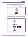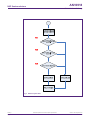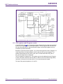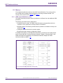
1
AN10918
NXP LPC Cortex-M3 IEC60335 Class B library
Rev. 01 — 1 March 2010
Application note
Document information
Info
Content
Keywords
NXP ARM Cortex-M3, IEC60335 Class B, VDE, LPC1700, LPC1300
Abstract
This application note describes the IEC60335 Class B certified library for
the NXP ARM Cortex-M3 family members. All tests implemented and the
library usage are described in detail.
AN10918
NXP Semiconductors
IEC60335 Class B library
Revision history
Rev
Date
Description
01
Initial version.
20100301
Contact information
For additional information, please visit: http://www.nxp.com
For sales office addresses, please send an email to: [email protected]
AN10918_1
Application note
All information provided in this document is subject to legal disclaimers.
Rev. 01 — 1 March 2010
© NXP B.V. 2010. All rights reserved.
2 of 68
AN10918
NXP Semiconductors
IEC60335 Class B library
1. Introduction
Nowadays, all home appliances require a certain level of protection to be taken in order
to avoid hazardous situations if the appliance fails. Since 2007 home appliances must
comply with the IEC60335 standard. Home appliance manufacturers therefore need to
ensure that the requirements are met.
This document describes the IEC60335 standard requirements with respect to software
for microcontrollers and the implementation of these requirements. NXP has developed a
software library for the NXP ARM Cortex-M3 family, based on these requirements and
this document discusses the tests and the usage of these tests in detail.
ATTENTION!
The usage of this library does not make a certified application of your project. It is still
necessary to have to have the complete application software certified.
This library should not be changed, and it should be used as explained. Otherwise, a
new certification for the changed parts will be necessary.
The library is usable, as-is, for all NXP ARM Cortex-M3 products, including those not
specifically mentioned in this application note.
1.1 How to read this application note
This application note is a guide in using and implementing the library functions provided.
It will first discuss the set requirements of the IEC60335 standard, and then briefly
discuss the products the library is developed for.
The main part of the document describes how the Class B tests are done and how it can
and should be implemented. Details on the tested peripherals are given in the last
chapter.
AN10918_1
Application note
All information provided in this document is subject to legal disclaimers.
Rev. 01 — 1 March 2010
© NXP B.V. 2010. All rights reserved.
3 of 68
AN10918
NXP Semiconductors
IEC60335 Class B library
2. IEC60335 Class B
The IEC60335 standard specifies design enhancements for home appliance
manufacturers that design appliances with electronic controls and controls using software
with respect to safe and reliable operation. This standard requires inclusion of features
that will avoid or at least minimize the change of hazardous situations when the
appliance fails.
Referring to IEC60730, this deals with standard various assets of safety and reliability
precautions required to be taken for all home appliances. Annex H of the IEC60730
standard software and hardware requirements is defined to be taken in order to comply
with this standard.
2.1 Software classification
Within the IEC60730 Annex H, details for testing and diagnostic implementation in
microcontroller software are classified as A, B or C.
• Class A: Control functions which are not intended to be relied upon for the safety of
the equipment
• Class B: Control functions intended to prevent unsafe operation of the controlled
equipment.
• Class C: Control functions which are intended to prevent special hazards (e.g.,
explosion of the controlled equipment, such as burner controls).
The majority of the home appliances, like white goods (refrigerator, dishwasher, cooker
etc.) and personal appliances (electrical tooth brush, shaver etc.), require the Class B
level of precautions.
The IEC60370 Class B specifies that measures must be taken to avoid software related
faults and errors in data and segments of the software that are safety related. Periodic
monitoring of the system therefore is required.
AN10918_1
Application note
All information provided in this document is subject to legal disclaimers.
Rev. 01 — 1 March 2010
© NXP B.V. 2010. All rights reserved.
4 of 68
AN10918
NXP Semiconductors
IEC60335 Class B library
2.2 Class B components
Table H.11.12.7 of IEC60730 Annex H specifies the components to be tested and
monitored during operation of the controller. Table 1 shows a summary of table
H.11.12.7.
Table 1.
Test
number
Component
Fault/error
In
library
1.1.
CPU registers
Stuck at
YES
1.3.
Program Counter
Stuck at
YES
2.
Interrupt handling and execution
No interrupt or too frequent
interrupt
YES
3.
Clock
Wrong frequency (for quartz
synchronized clock: harmonics/
subharmonics only)
YES
4.1.
Invariable memory
All single bit faults
YES
4.2.
Variable memory
DC Fault
YES
4.3.
Addressing (relevant to variable and
invariable memory)
Stuck at
YES
5.1.[1]
Internal data path
Stuck at
NO
5.2. [1]
Addressing
Wrong address
NO
6.
External communications
Hamming distance 3
NO
6.3.
Timing
Wrong point in time and
sequence
NO
7.[2]
AN10918_1
Application note
IEC60335 Class B tests as defined by IEC60730 Annex H
Input/output periphery
Fault conditions specified in H.27
NO
7.2.1.
[2]
A/D and D/A converters
Fault conditions specified in H.27
NO
7.2.2.
[2]
Analog multiplexer
Wrong addressing
NO
[1]
Only when using external memory
[2]
Production plausibility check
All information provided in this document is subject to legal disclaimers.
Rev. 01 — 1 March 2010
© NXP B.V. 2010. All rights reserved.
5 of 68
AN10918
NXP Semiconductors
IEC60335 Class B library
3. NXP ARM Cortex-M3 Microcontrollers
This chapter gives a general description of the NXP ARM Cortex-M3 family members for
which the IEC60335 Class B self-test libraries are written.
3.1 The NXP ARM Cortex-M3 microcontrollers
The LPC1700 and LPC1300 families are ARM Cortex-M3 (r2p0 version) based
microcontrollers for embedded applications requiring a high level of integration and low
power dissipation. The ARM Cortex-M3 is a next generation core that offers system
enhancements such as modernized debugging features and a higher level of support
block integration.
The LPC1700 family operates at up to a 120 MHz CPU frequency and the LPC1300
family operates up to 72 MHz. The ARM Cortex-M3 CPU incorporates a 3-stage pipeline
and uses a Harvard architecture with separate local instruction and data buses as well as
a third bus for peripherals. The ARM Cortex-M3 CPU also includes an internal pre-fetch
unit that supports speculative branches.
3.1.1 The ARM Cortex-M3 core
The ARM Cortex-M3 32-bit processor has been specifically developed to provide a highperformance, low-cost platform for a broad range of applications including
microcontrollers, automotive body systems, industrial control systems and wireless
networking. The Cortex-M3 processor provides outstanding computational performance
and exceptional system response to interrupts while meeting low cost requirements
through small core footprint, industry leading code density enabling smaller memories,
reduced pin count and low power consumption.
The central core of the Cortex-M3 processor, based on a 3-stage pipeline Harvard bus
architecture, incorporates advanced features including single cycle multiply and
hardware divide to deliver an outstanding efficiency of 1.25 DMIPS/MHz. The Cortex-M3
processor also implements the new Thumb-2 instruction set architecture which, when
combined with features such as unaligned data storage and atomic bit manipulation,
delivers 32-bit performance at a cost equivalent to modern 8- and 16-bit devices.
AN10918_1
Application note
All information provided in this document is subject to legal disclaimers.
Rev. 01 — 1 March 2010
© NXP B.V. 2010. All rights reserved.
6 of 68
AN10918
NXP Semiconductors
IEC60335 Class B library
Fig 1. The Cortex M3 core
3.2 Product options
Both the LPC1700 and LPC1300 are available in various configurations of memory sizes,
packages and peripherals.
Table 2 and Table 3 show the variety of products available.
3.2.1 The LPC1700
The peripheral complement of the LPC1700 family includes up to 512 kB of flash
memory, up to 64 kB of data memory, Ethernet MAC, USB Device/Host/OTG interface,
8-channel general purpose DMA controller, 4 UARTs, 2 CAN channels, 2 SSP
controllers, SPI interface, 3 I2C-bus interfaces, 2-input plus 2-output I2S-bus interface, 8channel 12-bit ADC, 10-bit DAC, motor control PWM, Quadrature Encoder interface, 4
general purpose timers, 6-output general purpose PWM, ultra-low power Real-Time
Clock (RTC) with separate battery supply, and up to 70 general purpose I/O pins.
The ARM Cortex-M3 includes three AHB-Lite buses, one system bus, and the I-code and
D-code buses, which are faster and are used similarly to TCM interfaces: one bus
dedicated for instruction fetch (I-code) and one bus for data access (D-code). The use of
two core buses allows for simultaneous operations if concurrent operations target
different devices.
The LPC1700 uses a multi-layer AHB matrix to connect the Cortex-M3 buses and other
bus masters to peripherals in a flexible manner that optimizes performance by allowing
peripherals on different slave ports of the matrix to be accessed simultaneously by
different bus masters.
APB peripherals are connected to the CPU via two APB buses using separate slave
ports from the multilayer AHB matrix. This allows for better performance by reducing
collisions between the CPU and the DMA controller. The APB bus bridges are configured
to buffer writes so that the CPU or DMA controller can write to APB devices without
always waiting for APB write completion.
AN10918_1
Application note
All information provided in this document is subject to legal disclaimers.
Rev. 01 — 1 March 2010
© NXP B.V. 2010. All rights reserved.
7 of 68
AN10918
NXP Semiconductors
IEC60335 Class B library
The LPC176x devices are available in an LQFP100 package while the LPC175x MCUs
are offered in an LQFP80 package. For a detailed peripheral options please see the
LPC1700 user manual (UM10360).
Table 2.
AN10918_1
Application note
LPC1700 option list
Product
Flash
RAM
Package
LPC1751
32 kB
8 kB
LQFP80
LPC1752
64 kB
16 kB
LQFP80
LPC1754
128 kB
32 kB
LQFP80
LPC1756
256 kB
32 kB
LQFP80
LPC1758
512 kB
32kB
LQFP80
LPC1759
512 kB
32 kB
LQFP80
LPC1764
128 kB
32 kB
LQFP100
LPC1765
256 kB
64 kB
LQFP100
LPC1766
256 kB
64 kB
LQFP100
LPC1767
512 kB
64 kB
LQFP100
LPC1768
512 kB
64 kB
LQFP100
All information provided in this document is subject to legal disclaimers.
Rev. 01 — 1 March 2010
© NXP B.V. 2010. All rights reserved.
8 of 68
AN10918
NXP Semiconductors
IEC60335 Class B library
3.2.2 The LPC1300
The peripheral complement of the LPC1300 family includes up to 32 kB of flash memory,
up to 8 kB of data memory, USB Device, one Fast mode plus I2C interface, one UART,
four general purpose timers, and up to 42 general purpose I/O pins.
The LPC1340 family members have on-chip bootloader drivers for USB MSC and HID
classes. It provides a host driverless USB bootloader supporting flash programming.
These USB drivers are also available though a simplified USB API and save up to 6 kB
extra flash memory space.
The ARM Cortex-M3 includes three AHB-Lite buses, one system bus and the I-code and
D-code buses which are faster and are used similarly to TCM interfaces: one bus
dedicated for instruction fetch (I-code) and one bus for data access (D-code). The use of
two core buses allows for simultaneous operations if concurrent operations target
different devices.
The LPC13xx products are available in either a LQFP48 or a HVQFN33 packages.
Table 3.
AN10918_1
Application note
LPC1300 options list
Product
Flash
RAM
Package
LPC1311
8 kB
2 kB
HVQFN33
LPC1313
32 kB
8 kB
LQFP48, HVQFN33
LPC1342
16 kB
4 kB
HVQFN33
LPC1343
32 kB
8 kB
LQFP48, HVQFN33
All information provided in this document is subject to legal disclaimers.
Rev. 01 — 1 March 2010
© NXP B.V. 2010. All rights reserved.
9 of 68
AN10918
NXP Semiconductors
IEC60335 Class B library
4. IEC60335 Class B library
The chapter gives an overview about the functionality of the various functions and
illustrates how the functions are implemented. It gives you knowledge about the library
and helps with understanding the self-test philosophy. Please note by changing any
library functionality it needs to be re-certified again. If a special part needs to be modified,
then there will be an explicit description and explanation.
4.1 POST and BIST
POST (Pre Operation System Test) means the testing as part of the start-up procedure.
These tests are destroyable, which means that the data contents are not restored after
executing the test. Also, in this state of application, there are normally no interrupts
active.
Note, at start-up all tests must be executed: CPU registers, PC, RAM and ROM. For this
reason special POST functions are available. The POST testing is developed such that it
reduces test time and therefore is monolithic and destroyable.
The Built-In Self-Test (BIST) is designed such that it will not modify the content of
program, data or registers. To avoid system failures in time critical applications, these
test are not monolithic. Functions are implemented for testing the variable and nonvariable in smaller blocks.
AN10918_1
Application note
All information provided in this document is subject to legal disclaimers.
Rev. 01 — 1 March 2010
© NXP B.V. 2010. All rights reserved.
10 of 68
AN10918
NXP Semiconductors
IEC60335 Class B library
4.2 CPU Register Test (1.1)
4.2.1 Test description
As described in chapter 5.1 the ARM Cortex-M3 core [3][5][8] has a number of registers
used during program execution. Nineteen of these registers are read/write.
Since these registers are all used during program execution in the various core operation
modes, they are tested for stuck-at faults and direct coupling faults.
These tests are to be executed as POST and BIST. POST testing is a destroyable test,
so the CPU registers will not be retained. Since the POST CPU register tests don’t retain
register data, it is mandatory to execute this test prior any other application or system
initialization. Preferably execute this test prior to branch to main. All tests are executed in
one routine, which allows the quickest test completion.
CPU BIST testing isn’t destroyable, so all data is restored after testing. To decrease test
time and therefore CPU resources, the CPU register BIST testing is parted in five
separate tests. The first three test the general purpose registers, the fourth tests the
stack pointer. To prevent the system from crashing, all interrupts and exceptions are
disabled while running this part of the CPU register BIST. The fifth and last BIST test is
testing the other special registers.
Note: All CPU register BIST tests are executed in Privileged mode.
Both BIST and POST use the same test methodology when testing the registers. First, a
pattern will be stored in the register, then read back and compared. Then, the inverse of
that pattern is stored in the register, read and compared.
The basic pattern used for the CPU register tests:
• Normal:
0xAAAA.AAAA
• Inverted: 0x5555.55555
AN10918_1
Application note
All information provided in this document is subject to legal disclaimers.
Rev. 01 — 1 March 2010
© NXP B.V. 2010. All rights reserved.
11 of 68
AN10918
NXP Semiconductors
IEC60335 Class B library
4.2.2 Test usage
This chapter describes the files used and summarizes all function calls used in CPU
register POST and BIST testing
These tests are developed in assembly code because most of the registers of the core
are not directly accessible from C code.
4.2.2.1 IEC60335_B_CPUregTest.h
File name
Function prototyping
IEC60335_B_CPUregTest.h
extern void _CPUregTestPOST(void);
extern void _CPUregTestLOW(void);
extern void _CPUregTestMID(void);
extern void _CPUregTestHIGH(void);
extern void _CPUregTestSP(void);
extern void _CPUregTestSPEC(void);
type_testResult IEC60335_CPUregTest_POST(void);
Type definition
IEC60335_CPUreg_struct
This header file contains all function prototypes and the structure type definition used
during the CPU register tests. It therefore enables the C source files to call the Assembly
source routines.
AN10918_1
Application note
All information provided in this document is subject to legal disclaimers.
Rev. 01 — 1 March 2010
© NXP B.V. 2010. All rights reserved.
12 of 68
AN10918
NXP Semiconductors
IEC60335 Class B library
4.2.2.2 IEC60335_B_CPUregTest.c
File name
Function prototyping
IEC60335_B_CPUregTest.c
type_testResult IEC60335_CPUregTest_POST (void)
Structure definition
IEC60335_CPUreg_struct CPUregTestPOST_struct
IEC60335_CPUreg_struct CPUregTestBIST_struct
This file is responsible for the test structure definitions. The main CPU register BIST
function is located in this file.
Function:
type_testResult IEC60335_testResult IEC60335_CPUregTest_POST
Purpose:
The type_testResult IEC60335_CPUregTest_POST (void) function executes the full POST
test. This test should be called through an exception for operating in Privileged mode.
After this test is executed, the CPUregTestBIST_struct contains the full pass/fail indication,
testPassed. Also the testState will be updated, which indicates the passing tests
according to Table 5.
Return value:
IEC60335_testPassed
IEC60335_testFailed
Important file or function notifications:
• The IEC60335_CPUregTest_POST may only be executed in Privileged (Handler or
Thread) mode, so it must be called during an exception.
• Test pass/fail available through function return and it available in testPassed
structure member.
AN10918_1
Application note
All information provided in this document is subject to legal disclaimers.
Rev. 01 — 1 March 2010
© NXP B.V. 2010. All rights reserved.
13 of 68
AN10918
NXP Semiconductors
IEC60335 Class B library
4.2.2.3 IEC60335_B_CPUregTestBIST_nnn.asm
File name
Function prototyping
[1]
IEC60335_B_CPUregTestBIST_nnn .asm
void _CPUregTestLOW(void);
void _CPUregTestMID(void);
void _CPUregTestHIGH(void);
void _CPUregTestSP(void);
void _CPUregTestSPEC(void);
[1]
The nnn in the .asm file names must be replaced by a compiler indicator.
gnu = GNU GCC compiler
arm = ARM RealView compiler
iar = IAR EWARM compiler
This file contains all routines for testing the CPU registers during program execution and
it gives the user access to the required functions used by the CPU register BIST testing.
The registers tested by the test functions are listed in Table 4.
Table 4.
CPU register BIST functions
Test function name
Register tested
_CPUregTestLOW
R0 - R7
_CPUregTestMID
R4 – R10
_CPUregTestHIGH
R8 – R12
_CPUregTestSP
R13, stackpointer (Only MSP)
_CPUregTestSPEC
LR, APSR, PRIMASK, FAULTMASK and BASEPRI
After each individual test, the test structure is updated and therefore contains the latest
test values. Each test will reset the testPassed structure member and write the new pass
or fail status. The testState member will also be updated after each test with the status of
all passing tested registers.
Only the Main Stack Pointer (MSP) 1 MSP is BIST tested during this test therefore only
the MSP may be used in safety critical applications.
Important file or function notifications:
• All functions can be called at any time but must execute in Privileged operation mode
• After test execution, the passing tests will be given a PASS bit in the
CPUregTestBIST_struct testState member according to Table 5
• After test execution, and all containing tests, all passes CPUregTestBIST_struct
testPassed will be set to IEC60335_testPassed = 1
• Only MSP may be used in safety critical applications.
1.
AN10918_1
Application note
See chapter 5.2
All information provided in this document is subject to legal disclaimers.
Rev. 01 — 1 March 2010
© NXP B.V. 2010. All rights reserved.
14 of 68
AN10918
NXP Semiconductors
IEC60335 Class B library
4.2.2.4 IEC60335_B_CPUregTestPOST_nnn.asm
File name
Function prototyping
[1]
IEC60335_B_CPUregTestPOST_nnn .asm
[1]
void _CPUregTestPOST(void);
The nnn in the .asm file names must be replaced by a compiler indicator.
gnu = GNU GCC compiler
arm = ARM RealView compiler
iar = IAR EWARM compiler
This file contains the POST testing routing of the CPU registers. It gives the user access
to the CPU register POST.
Important file or function notifications:
• The _CPUregTestPOST function must be executed prior to the branch to main. It
should also execute in Privilege Thread mode.
• After test execution, the passing tests will be given a PASS bit in the
CPUregTestPOST_struct testState structure member, according to Table 5.
• After test execution, and all containing tests all passes, CPUregTestPOST_struct
testPassed will be set to IEC60335_testPassed = 1.
AN10918_1
Application note
All information provided in this document is subject to legal disclaimers.
Rev. 01 — 1 March 2010
© NXP B.V. 2010. All rights reserved.
15 of 68
AN10918
NXP Semiconductors
IEC60335 Class B library
4.2.2.5 CPU register test numbers
During both the BIST and POST testing the testState member of the test structure is
updated with the passing tests. The table below depicts the tested register and its
corresponding bit value found in the testState.
Table 5.
AN10918_1
Application note
CPU register test table
Test number
Hexadecimal bit
value
Register
Bits tested
0
0x0000 0001
R0
31:0
1
0x0000 0002
R1
31:0
2
0x0000 0004
R2
31:0
3
0x0000 0008
R3
31:0
4
0x0000 0010
R4
31:0
5
0x0000 0020
R5
31:0
6
0x0000 0040
R6
31:0
7
0x0000 0080
R7
31:0
8
0x0000 0100
R8
31:0
9
0x0000 0200
R9
31:0
10
0x0000 0400
R10
31:0
11
0x0000 0800
R11
31:0
12
0x0000 1000
R12
31:0
13
0x0000 2000
R13 (default SP, MSP) 31:2
14
0x0000 4000
R13 (alternative SP)
31:2
15
0x0000 8000
R14 (LR)
31:0
16
0x0001 0000
APSR
31:27
17
0x0002 0000
PRIMASK
0
18
0x0004 0000
FAULTMASK
0
19
0x0008 0000
BASEPRI
7:3
All information provided in this document is subject to legal disclaimers.
Rev. 01 — 1 March 2010
© NXP B.V. 2010. All rights reserved.
16 of 68
AN10918
NXP Semiconductors
IEC60335 Class B library
4.3 Program Counter (PC) Test (1.3)
4.3.1 Test description
The PC test checks whether the PC is able to branch throughout the whole program and
data memory space. To test the branching dummy functions are allocated throughout the
whole used program and data memory space.
The allocation of the PC dummy test functions are placed accordingly by use of sections
defined in the linker file.
The PC test routines call the dummy functions and check the returned value. Each
dummy function will return a unique value. Thereby it is possible to check if the PC has
jumped to the correct address.
Note that an enabled memory protection unit may trigger an exception when dummy
functions are executable code areas that are protected.
In principle, the test results always show as okay, because a defective program counter
results in program crashes in any way.
There are two different implementations for this test available. One is for BIST and the
other for POST. The POST will check each dummy function at once. This is implemented
by a loop. The BIST will only test one dummy function per call. All functions will be called
after each other like a ring buffer.
Loop:
Call every Dummyjunction
after each other
Set result TRUE
Set result FALSE
Return result
Fig 2. PC POST (left) and PC BIST (right) test flow diagram
AN10918_1
Application note
All information provided in this document is subject to legal disclaimers.
Rev. 01 — 1 March 2010
© NXP B.V. 2010. All rights reserved.
17 of 68
AN10918
NXP Semiconductors
IEC60335 Class B library
4.3.2 Test usage
This chapter describes the usage of the PC POST and BIST.
4.3.2.1 IEC60335_B_ProgramCounterTest.h
File name
Function prototyping
IEC60335_B_ProgramCounterTest.h
type_testResult IEC60335_B_PCTest_POST(void);
type_testResult IEC60335_B_PCTest_BIST(void);
This header file contains all function prototypes used during the PC tests.
4.3.2.2 IEC60335_B_ProgramCounterTest.c
File name
Definitions
IEC60335_B_ProgramCounterTest.c
RET_FCT_A = 1
RET_FCT_B = 2
RET_FCT_C = 3
RET_FCT_D = 5
RET_FCT_E = 7
RET_FCT_F = 11
Global variable
UINT32 IEC60335_B_PCTest_lastFctTested
Functions
type_testResult IEC60335_B_PCTest_POST(void)
type_testResult IEC60335_B_PCTest_BIST(void)
The PC test should be done pre-operation (POST) and during program execution (BIST).
The PC POST and BIST functions are to be called in the corresponding state of the
controller.
AN10918_1
Application note
All information provided in this document is subject to legal disclaimers.
Rev. 01 — 1 March 2010
© NXP B.V. 2010. All rights reserved.
18 of 68
AN10918
NXP Semiconductors
IEC60335 Class B library
Function:
type_testResult IEC60335_B_PCTest_POST(void)
Purpose:
This function should be executed prior to running the main application. It will call the test
functions throughout the program and data memory and check the return value against
the expected value.
Return value:
IEC60335_testPassed
IEC60335_testFailed
Function:
type_testResult IEC60335_B_PCTest_BIST(void)
Purpose:
The PC BIST function IEC60335_B_PCTest_BIST(void) executes at every call one PC
test, saves the current executed test, and returns a PASS/FAIL. It will automatically run
through all six tests.
Return value:
IEC60335_testPassed
IEC60335_testFailed
AN10918_1
Application note
All information provided in this document is subject to legal disclaimers.
Rev. 01 — 1 March 2010
© NXP B.V. 2010. All rights reserved.
19 of 68
AN10918
NXP Semiconductors
IEC60335 Class B library
4.4 Interrupt Handling and Execution Test (2)
4.4.1 Test description
The test for interrupt handling and execution is application dependent. In this test, the
library delivers some templates to enable the users testing the functionality in an abstract
way.
The interrupts will be checked with the aid of counter variables. The different interrupts,
which are observed by counter mechanisms, should have individual up-counting values
instead of simply adding one.
To check the interrupts, the counter value has to be checked cyclically in a known
equidistant time and compared to boundaries estimated by the user. A timer interrupt
service handler should solve this.
Burst interrupt?
Burst time passed?
Interrupt counter in
boundaries?
Set result TRUE
Set Result FALSE
Return from
function
Fig 3. Interrupt
The interrupt check routine first checks the interrupt configuration for the type of interrupt.
The test usage details are described in chapter 4.4.2.
AN10918_1
Application note
All information provided in this document is subject to legal disclaimers.
Rev. 01 — 1 March 2010
© NXP B.V. 2010. All rights reserved.
20 of 68
AN10918
NXP Semiconductors
IEC60335 Class B library
If the interrupt that needs to be checked is a burst interrupt, the routine will check if the
time to wait for all interrupts has elapsed. If the time has passed, it will check the interrupt
count to be within the boundaries. If not, the check function will return directly, without
setting any Result.
If the interrupt to check is not a burst interrupt, the routine will check the interrupt counter
to be within the bound directly.
4.4.2 Test usage
4.4.2.1 IEC60335_B_Interrupts.h
File name
Type definition
IEC60335_B_Interrupts.h
type_InterruptTest
[1]
Function prototyping
void IEC60335_InitInterruptTest
(
type_InterruptTest *pIRQ,
UINT32 lowerBound,
UINT32 upperBound,
UINT32 individualValue
);
void IEC60335_InterruptOcurred
(
type_InterruptTest *pIRQ
);
type_testResult IEC60335_InterruptCheck
(
type_InterruptTest *pIRQ
);
[1]
See the detailed type description in Table 6
The IEC60335_B_Interrupts header file contains the function prototypes of the interrupt
testing. A type defined structure contains all variables needed for interrupt testing.
AN10918_1
Application note
All information provided in this document is subject to legal disclaimers.
Rev. 01 — 1 March 2010
© NXP B.V. 2010. All rights reserved.
21 of 68
AN10918
NXP Semiconductors
IEC60335 Class B library
Table 6.
Type_InterruptTest type description
Member name
Description
UINT32 count
The counter variable
UINT32 lower
The estimated minimum count value of the interrupt concurrencies
UINT32 upper
The estimated maximum count value of the interrupt concurrencies
UINT32 individualValue
The individual up-counting value
BOOL CountOverflow
Counter overflow bit
BOOL cyclic
The time count that has to be waited, before the check is done
UINT32 minTime
4.4.2.2 IEC60335_B_Interrupts.c
File name
Function
IEC60335_B_Interrupts.c
void IEC60335_InitInterruptTest
(
type_InterruptTest *pIRQ,
UINT32 lowerBound,
UINT32 upperBound,
UINT32 individualValue
)
void IEC60335_InterruptOcurred
(
type_InterruptTest *pIRQ
)
type_testResult IEC60335_InterruptCheck
(
type_InterruptTest *pIRQ
)
This file contains the functions needed for the Interrupt testing.
AN10918_1
Application note
All information provided in this document is subject to legal disclaimers.
Rev. 01 — 1 March 2010
© NXP B.V. 2010. All rights reserved.
22 of 68
AN10918
NXP Semiconductors
IEC60335 Class B library
Function:
void IEC60335_InitInterruptTest
(
type_InterruptTest *pIRQ,
UINT32 lowerBound,
UINT32 upperBound,
UINT32 individualValue
)
Purpose:
The IEC60335_InitInterruptTest function will initialize the interrupt test structure.
This function must be called prior to any interrupt initializations.
Input variables:
type_InterruptTest *pIRQ
This structure pointer is used to set the default values to the interrupt test structure
members during the interrupt test initialization.
UINT32 lowerBound
The estimated minimum count value of the interrupt concurrencies.
UINT32 upperBound
The estimated maximum count value of the interrupt concurrencies.
UINT32 individualValue
The internal individual up-counting value.
Return value:
None
AN10918_1
Application note
All information provided in this document is subject to legal disclaimers.
Rev. 01 — 1 March 2010
© NXP B.V. 2010. All rights reserved.
23 of 68
AN10918
NXP Semiconductors
IEC60335 Class B library
Function:
void IEC60335_InterruptOcurred
(
type_InterruptTest *pIRQ
)
Purpose:
This function must be called from any interrupt service handler which has to be tested.
Input variables:
type_InterruptTest *pIRQ
Pointer to the interrupt test structure.
Return value:
None
Function:
type_testResult IEC60335_InterruptCheck
(
type_InterruptTest *pIRQ
)
Purpose:
This function must be called from any interrupt service handler which has to be tested.
Input variables:
type_InterruptTest *pIRQ
Pointer to the interrupt test structure.
Return value:
IEC60335_testPassed
IEC60335_testFailed
AN10918_1
Application note
All information provided in this document is subject to legal disclaimers.
Rev. 01 — 1 March 2010
© NXP B.V. 2010. All rights reserved.
24 of 68
AN10918
NXP Semiconductors
IEC60335 Class B library
4.5 Clock System Test (3)
4.5.1 Test description
This test is intended to check the CPU clock source and frequency. This requires a
second independent clock source. For a part of the NXP ARM Cortex-M3 family, the only
possibility to get interrupts triggered, sourced by an independent clock, is to use the RTC
peripheral.
Three test functions are implemented, and the first one is cyclically called from the main
loop of the user application.
As depicted in the Fig 4, the main loop function checks both the timer and RTC interrupt
occurrence functions. If one or both of them are missing within a rough time frame, which
has to be estimated empirically, the function will return failed as result. This function also
checks the result of the timer check, which is performed by the RTC function.
Main - loop
1
2
Tests the RTC occurrence
Tests the timer occurrence
3
Tests the timer interrupt speed
Timer interrupt
(sourced by cpu
clk)
RTC interrupt.
(sourced by
independent clk)
Fig 4. Clock system test flow
The second function is intended to be called from a timer interrupt service handler. This
Timer needs to have the same clock source as the CPU.
The last function is intended to be called from the RTC interrupt service handler. This
function is intended to check the frequency of the timer interrupts.
AN10918_1
Application note
All information provided in this document is subject to legal disclaimers.
Rev. 01 — 1 March 2010
© NXP B.V. 2010. All rights reserved.
25 of 68
AN10918
NXP Semiconductors
IEC60335 Class B library
The timer simply counts how often the timer interrupt has occurred. This value is then
checked by the RTC function. Additionally, it sets the occurrence semaphore, which is
used for occurrence recognition inside of the main function. See Fig 5.
Fig 5. Setting the occurrence semaphore
The RTC function also sets an occurrence semaphore, to be tested from the main
function. Then it checks the timer counter variable to be within the estimated boundaries.
The result of this check is stored into a result semaphore.
Fig 6. Setting semaphore and boundary check
AN10918_1
Application note
All information provided in this document is subject to legal disclaimers.
Rev. 01 — 1 March 2010
© NXP B.V. 2010. All rights reserved.
26 of 68
AN10918
NXP Semiconductors
IEC60335 Class B library
Fig 7. Main-loop test flow
AN10918_1
Application note
All information provided in this document is subject to legal disclaimers.
Rev. 01 — 1 March 2010
© NXP B.V. 2010. All rights reserved.
27 of 68
AN10918
NXP Semiconductors
IEC60335 Class B library
4.5.2 Test usage
4.5.2.1 IEC60335_B_ClockTest.h
File name
Function prototyping
IEC60335_B_ClockTest.h
void IEC60335_initClockTest
(
UINT32 timerOccThreshold,
UINT32 rtcOccThreshold,
UINT32 timerLowerBound,
UINT32 timerUpperBound
)
type_testResult IEC60335_Clocktest_MainLoopHandler(void)
void IEC60335_Clocktest_TimerIntHandler(void)
void IEC60335_Clocktest_RTCHandler(void)
The IEC60335_B_ClockTest.h file contains all prototypes needed for the ClockTest.
4.5.2.2 IEC60335_B_ClockTest.c
File name
Type definition
IEC60335_B_ClockTest.c
type_ClockTest
[1]
Functions
void IEC60335_resetClockTest(void)
void IEC60335_initClockTest
(
UINT32 timerOccThreshold,
UINT32 rtcOccThreshold,
UINT32 timerLowerBound,
UINT32 timerUpperBound
)
type_testResult IEC60335_Clocktest_MainLoopHandler(void)
void IEC60335_Clocktest_TimerIntHandler(void)
type_testResult IEC60335_Clocktest_MainLoopHandler(void)
void IEC60335_Clocktest_RTCHandler(void)
[1]
AN10918_1
Application note
Structure members described in Table 7
All information provided in this document is subject to legal disclaimers.
Rev. 01 — 1 March 2010
© NXP B.V. 2010. All rights reserved.
28 of 68
AN10918
NXP Semiconductors
IEC60335 Class B library
Table 7.
type_ClockTest structure
Member name
Description
UINT32 timerTestThreshold
Used in the mainloop function, defines the number of calls to
start occurrence test
UINT32 rtcTestThreshold
Used in the mainloop function, defines the number of calls to
start occurrence test
UINT32 rtcOccCounter
Counter variable for the mainloop, if value reached the defined
threshold, the occurrence test is started
UINT32 timerOccCounter
Counter variable for the mainloop, if value reached the defined
threshold, the occurrence test is started
BOOL timerOccured
This bool will be set in the timer function, and is reset during
occurrence test
BOOL rtcOccured
This bool will be set in the rtc function, and is reset during
occurrence test
UINT32 timerCounter
The counter Variable, to test the timer to be within its
boundaries
UINT32 timerBoundLower
The estimated minimum count of cycle occurrences (Threshold
for timer test).
UINT32 timerBoundUpper
The estimated maximum count of cycle occurrences (Threshold
for timer test).
BOOL timerOutOfBounds
Within this bool, the rtc timer test signals the error state to the
main function
BOOL timerCounterOverflow
Reflects, if the TimerCounter was flown over due to an error
Function:
void IEC60335_resetClockTest(void)
Purpose:
The IEC60335_resetClockTest function clears and resets all used Clock Test variables
Return value:
None
AN10918_1
Application note
All information provided in this document is subject to legal disclaimers.
Rev. 01 — 1 March 2010
© NXP B.V. 2010. All rights reserved.
29 of 68
AN10918
NXP Semiconductors
IEC60335 Class B library
Function:
void IEC60335_initClockTest
(
UINT32 timerOccThreshold,
UINT32 rtcOccThreshold,
UINT32 timerLowerBound,
UINT32 timerUpperBound
)
Purpose:
This function initiates the various variables used during the Clock Test.
Input variables:
UINT32 timerOccThreshold
The timerOccThreshold variable initiates the threshold value that defines the number
of calls that started the timer occurrence test.
UINT32 rtcOccThreshold
The rtcOccThreshold variable initiates the threshold value that defines the number of
calls that started the RTC occurrence test.
UINT32 timerLowerBound
This variable sets the lower bound value of the number of timer or RTC test occurrences.
UINT32 timerUpperBound
This variable sets the upper bound value of the number of timer or RTC test occurrences.
Return value:
None
AN10918_1
Application note
All information provided in this document is subject to legal disclaimers.
Rev. 01 — 1 March 2010
© NXP B.V. 2010. All rights reserved.
30 of 68
AN10918
NXP Semiconductors
IEC60335 Class B library
Function:
type_testResult IEC60335_Clocktest_MainLoopHandler(void)
Purpose:
This function represents the part of the IEC60335 Class B clock test that must be
executed within the main loop.
This function tests the following criteria
• The clock test timer interrupts were triggered
• The clock test RTC interrupt was triggered
• In any of the two interrupts an error was detected.
Return value:
IEC60335_testPassed
IEC60335_testFailed
Important function notifications:
• This function must be called once inside the main loop.
• For this function, it is necessary to estimate the count of how often this function could
be called. This is important to find valid threshold values, which are used to test timer
and RTC interrupt occurrence.
AN10918_1
Application note
All information provided in this document is subject to legal disclaimers.
Rev. 01 — 1 March 2010
© NXP B.V. 2010. All rights reserved.
31 of 68
AN10918
NXP Semiconductors
IEC60335 Class B library
Function:
void IEC60335_Clocktest_TimerIntHandler(void)
Purpose:
This function is intended to use as a timer interrupt service handler or to be called once
inside the timer interrupt service handler.
Return value:
None
Function:
void IEC60335_Clocktest_RTCHandler(void)
Purpose:
This function should be called inside the custom RTC interrupt service handler. It can't be
used as a service handler by itself, because of the return value that has to be evaluated
after the call.
This function tests the timer-time-frame, in this case the CPU frequency.
Also, this function checks if the main loop function was called.
Return value:
None
AN10918_1
Application note
All information provided in this document is subject to legal disclaimers.
Rev. 01 — 1 March 2010
© NXP B.V. 2010. All rights reserved.
32 of 68
AN10918
NXP Semiconductors
IEC60335 Class B library
4.6 Invariable memory Test (4.1)
4.6.1 Test description
The invariable memory must be checked for single bit faults. During POST testing the
complete flash memory is tested. During BIST testing it is advisable to test the Flash
memory in smaller segments to prevent the CPU being blocked.
4.6.1.1 Multiple Input Signature Register
The NXP Cortex-M3 family has an integrated flash module that incorporates a 128-bit
signature generator, called the Multiple Input Signature Register (MISR).
This MISR can be used for generating a signature of the used safety critical memory
region.
Since this module is integrated in the flash module, it generates a signature faster than
when implemented in software.
A signature can be generated for any part of the flash contents. The address range to be
used for the signature generation is defined by writing the start address to the FMSSTART
register and the stop address to the FMSSTOP register.
The flash address should first be aligned with a flash word (128 bits). In the array this is
done by right-shifting the start and stop address by 4.
/* align flash address to refer the flash word in the array */
startAddr = (startAddr >> 4) & 0x0001ffff;
length
= ((startAddr + length) >> 4) & 0x0001ffff;
/* write start address of the flash contents to the register*/
LPC_FMC->FMSSTART = startAddr;
/* write stop address of the flash contents to the register, start generating
the signature*/
LPC_FMC->FMSSTOP = length | MISR_START;
The signature generation is started by writing ‘1’ to the MISR_START bit (17) in the
FMSSTOP register.
Since the MISR is implemented in hardware, it is much faster than doing the same MISR
check in software. The time that the signature generation takes is proportional to the
address range for which the signature is generated.
AN10918_1
Application note
All information provided in this document is subject to legal disclaimers.
Rev. 01 — 1 March 2010
© NXP B.V. 2010. All rights reserved.
33 of 68
AN10918
NXP Semiconductors
IEC60335 Class B library
4.6.1.2 Signature generation time
A safe estimation for the duration of the signature generation is
TMISR
(1)
⎞
⎛ 60ns
= int ⎜⎜
+ 3 ⎟⎟ × (FMSSTOP − FMSSTART + 1)
⎠
⎝ Tcclk
with Tcclk the core clock. See the device user manual for more information on the clock
system.
After completion of the hardware MISR the 128-bit signature can be read from the
FMSW0…FMSW3 registers.
4.6.1.3 Signature verification
The signatures generated by the hardware MISR must be verified and equal to the
reference signatures. The algorithm for deriving the reference signatures is illustrated in
the pseudo code below.
Sign_word0
Sign_word1
Sign_word2
Sign_word3
=
=
=
=
0
0
0
0
FOR address = FMSTART TO FMSTOP
{
nextSign_word0 = flashWord_word0 XOR (Sign_word0>>1) XOR (Sign_word1<<31)
nextSign_word1 = flashWord_word1 XOR (Sign_word1>>1) XOR (Sign_word2<<31)
nextSign_word2 = flashWord_word2 XOR (Sign_word2>>1) XOR (Sign_word3<<31)
nextSign_word3 = flashWord_word3 XOR (Sign_word3>>1)
XOR (Sign_word0 AND 1<<29) << 2
XOR (Sign_word0 AND 1<<27) << 4
XOR (Sign_word0 AND 1<<2) << 29
XOR (Sign_word0 AND 1<<0) << 31
Sign_word0
Sign_word1
Sign_word2
Sign_word3
}
=
=
=
=
nextSign0
nextSign1
nextSign2
nextSign3
Important notification:
The hardware MISR signature generator is blocking for the flash, this means no flash
read or write access is possible during signature generation. The MISR Code should run
from SRAM. It is therefore advisable to make sure while using the hardware MISR the
flash will not be accessed.
4.6.1.4 Critical content
If there is a stored critical constant periodically used in critical calculations, then it is
necessary to check this variable before every usage.
Refer to chapter 4.8 Secure Data storage.
AN10918_1
Application note
All information provided in this document is subject to legal disclaimers.
Rev. 01 — 1 March 2010
© NXP B.V. 2010. All rights reserved.
34 of 68
AN10918
NXP Semiconductors
IEC60335 Class B library
4.6.2 Test usage
This chapter explains how the invariable testing is implemented and can be used.
4.6.2.1 IEC60335_B_FlashTest.h
File name
Function prototyping
IEC60335_B_FlashTest.h
void StartHardSignatureGen
(
UINT32 startAddr,
UINT32 length,
FlashSign_t *ResultSign
);
void StartSoftSignatureGen
(
UINT32 startAddr,
UINT32 length,
FlashSign_t *ResultSign
);
type_testResult IEC60335_FLASHtest_BIST
(
UINT32 startAddr,
UINT32 length,
FlashSign_t *TestSign,
UINT8 selectHS
);
type_testResult IEC60335_FLASHtest_POST (UINT32 size);
type_testResult IEC60335_testSignatures
(
FlashSign_t *sign1,
FlashSign_t *sign2
);
Type definition
FlashSign_t
Definitions
SIZE32K = 0x00007FFF
SIZE64K = 0x0000FFFF
SIZE128K = 0x0001FFFF
SIZE256K = 0x0003FFFF
SIZE512K = 0x0007FFFF
FLASH_HARD_SIGN = 1
FLASH_SOFT_SIGN = 2
TESTSIGN_W0 = 0
TESTSIGN_W1 = 0
TESTSIGN_W2 = 0
TESTSIGN_W3 = 0
MISR_START = (1<<17)
EOM = (0x01<<2)
AN10918_1
Application note
All information provided in this document is subject to legal disclaimers.
Rev. 01 — 1 March 2010
© NXP B.V. 2010. All rights reserved.
35 of 68
AN10918
NXP Semiconductors
IEC60335 Class B library
Functions
All functions are described in detail in chapter 4.6.2.2
Type definitions
A type FlashSign_t is defined, this type contains four UINT32 variables named
word0…word3. These four words represent the 128 bits used for the hardware and
software 128-bit signature generation.
Definitions
The various flash sizes available on the NXP Cortex-M3 family are defined, so that the
user can easily test all flash onboard the chosen family member.
There are two defines which differentiate between the hardware or software generation,
used by the IEC60335_FLASHtest_BIST function.
FLASH_HARD_SIGN indicates the usage of the hardware signature generator, and
FLASH_SOFT_SIGN the software signature generator.
The TESTSIGN_W0…TESTSIGN_W3 variable definition can be used by the user to set a
predefined signature.
MISR_START is the hardware MISR start bit in the FMC FMSSTOP register.
EOM is the END OF MISR status in the FMC STATUS register
AN10918_1
Application note
All information provided in this document is subject to legal disclaimers.
Rev. 01 — 1 March 2010
© NXP B.V. 2010. All rights reserved.
36 of 68
AN10918
NXP Semiconductors
IEC60335 Class B library
4.6.2.2 IEC60335_B_FlashTest.c
File name
Function prototyping
IEC60335_B_FlashTest.c
void StartHardSignatureGen
(
UINT32 startAddr,
UINT32 length,
FlashSign_t *ResultSign
);
void StartSoftSignatureGen
(
UINT32 startAddr,
UINT32 length,
FlashSign_t *ResultSign
);
type_testResult IEC60335_FLASHtest_BIST
(
UINT32 startAddr,
UINT32 length,
FlashSign_t *TestSign,
UINT8 selectHS
);
type_testResult IEC60335_FLASHtest_POST (UINT32 size);
type_testResult IEC60335_testSignatures
(
FlashSign_t *sign1,
FlashSign_t *sign2
);
Structure definitions
FlashSign_t IEC60335_Flash_Sign_POST
FlashSign_t IEC60335_Flash_Sign_BIST
AN10918_1
Application note
All information provided in this document is subject to legal disclaimers.
Rev. 01 — 1 March 2010
© NXP B.V. 2010. All rights reserved.
37 of 68
AN10918
NXP Semiconductors
IEC60335 Class B library
Function:
void StartHardSignatureGen
(
UINT32 startAddr,
UINT32 length,
FlashSign_t *ResultSign
);
Purpose:
This function starts the execution of the hardware signature generation. It will do the
signature generation from the start address (startAddr) with a length (length). After
completion the signature will be copied to the location the pResultSign pointer points
to.
Input variables:
UINT32 startAddr
This variable is the starting address of where the signature generation will start.
UINT32 length
The length variable is the region size to use for the signature generation.
FlashSign_t *pResultSign
The result after generation completion will be put in the pointed location by the
pResultSign pointer.
Return value:
None
Important notification:
This function is BLOCKING. It blocks all access to the Flash memory. It is advisable to
make sure no flash memory needs to be accessed during the execution of this function.
The time required for this function is explained in the test description chapter.
AN10918_1
Application note
All information provided in this document is subject to legal disclaimers.
Rev. 01 — 1 March 2010
© NXP B.V. 2010. All rights reserved.
38 of 68
AN10918
NXP Semiconductors
IEC60335 Class B library
Function:
void StartSoftSignatureGen
(
UINT32 startAddr,
UINT32 length,
FlashSign_t *ResultSign
);
Purpose:
This function starts the execution of the software signature generation. It will do the
signature generation from the start address (startAddr) with a length (length).
The algorithm explained in the test description chapter is used for generation of the
software signature.
This function can be used for the reference signature with which the hardware generated
signature must be equal to.
After completion the signature will be copied to the location the pResultSign pointer
points to.
Input variables:
UINT32 startAddr
This variable is the starting address of where the signature generation will start.
UINT32 length
The length variable is the region size to use for the signature generation.
FlashSign_t *pResultSign
The result after generation completion will be put in the pointed location by the
pResultSign pointer.
Return value:
None
AN10918_1
Application note
All information provided in this document is subject to legal disclaimers.
Rev. 01 — 1 March 2010
© NXP B.V. 2010. All rights reserved.
39 of 68
AN10918
NXP Semiconductors
IEC60335 Class B library
Function:
type_testResult IEC60335_FLASHtest_BIST
(
UINT32 startAddr,
UINT32 length,
FlashSign_t *TestSign,
UINT8 selectHS
);
Purpose:
This is the general IEC60335 flash test function for BIST. It must be run periodically for
testing the safety critical region. The start address and region length is passed as well as
the reference signature to which the newly generated signature must match.
The user can select whether the hardware or software generator will be use during flash
BIST.
The comparison of the reference signature and the generated signature is integrated in
this function and therefore it will return a pass or fail for this test.
Input variables:
UINT32 startAddr
This variable is the starting address of where the signature generation will start.
UINT32 length
The length variable is the region size to be used for the signature generation.
FlashSign_t *TestSign
Pointer to the reference signature.
UINT8 selectHS
Hardware or software signature generation selection byte, FLASH_HARD_SIGN or
FLASH_SOFT_SIGN should be used.
Return value:
IEC60335_testPassed
IEC60335_testFailed
AN10918_1
Application note
All information provided in this document is subject to legal disclaimers.
Rev. 01 — 1 March 2010
© NXP B.V. 2010. All rights reserved.
40 of 68
AN10918
NXP Semiconductors
IEC60335 Class B library
Function:
type_testResult IEC60335_FLASHtest_POST
(
UINT32 size
);
Purpose:
This is the general IEC60335 flash test function for POST. This function will generate a
signature with the hardware generator over the complete flash of the chosen family
member.
The generated signature will be tested against the signature predefined by the user in the
definitions TESTSIGN_W0…TESTSIGN_W3.
After comparison of the signatures a pass or fail be returned.
Input variables:
UINT32 size
With this variable the user can define the size of the chosen family member.
Return value:
IEC60335_testPassed
IEC60335_testFailed
AN10918_1
Application note
All information provided in this document is subject to legal disclaimers.
Rev. 01 — 1 March 2010
© NXP B.V. 2010. All rights reserved.
41 of 68
AN10918
NXP Semiconductors
IEC60335 Class B library
Function:
type_testResult IEC60335_testSignatures
(
FlashSign_t *sign1,
FlashSign_t *sign2
);
Purpose:
This function compares two signatures and returns a pass or fail if equal or not.
Input variables:
FlashSign_t *sign1
Pointer to the first signature to be tested.
FlashSign_t *sign2
Pointer to the second signature to be tested.
Return value:
IEC60335_testPassed
IEC60335_testFailed
AN10918_1
Application note
All information provided in this document is subject to legal disclaimers.
Rev. 01 — 1 March 2010
© NXP B.V. 2010. All rights reserved.
42 of 68
AN10918
NXP Semiconductors
IEC60335 Class B library
4.7 Variable memory (4.2)
4.7.1 Test description
The variable memory (SRAM) must be tested for direct coupling and stuck-at faults. A
pattern therefore must be written and checked. This pattern is chosen such that it could
determine not only stuck-at faults but also direct coupling and even retention faults.
The March test algorithm is developed for efficient testing and detecting direct coupling
and stuck-at faults in the variable memory, or in this case RAM, array.
The March algorithm used during the variable memory testing is depicted in Fig 9. The
algorithm can be divided in 8 individual tests, called March tests 0 to 8. Each test has an
even and an odd test.
Even represents even addressing and odd represents odd addressing during the test,
indicated as nnnn in Fig 8. Increasing and decreasing addressing is indicated by use of
an up pointing or down pointing arrow. Read or write execution is indicated by r or w.
There are two patterns used during the variable memory test, the dbg (0x5555.5555) and
the dbgN (0xAAAA.AAAA) pattern. The pattern layout depends on the invariable memory
structure.
March x_nnnn
0x00
y
x = March test number, nnnn = even or odd address
y = r (Read) or w (Write)
Read/Write direction, incremental, decremental
01010101 = Pattern dbg, 0x5555.5555
0xFF
10101010 = Pattern dbgN, 0xAAAA.AAAA
Fig 8. Algorithm flow-diagram test example
This algorithm is designed to cover both stuck-at faults and direct coupling faults in the
fastest possible way.
March tests 0 and 1 test in increasing addressing order whether the full tested variable
memory region dbg pattern is written and read correctly. This covers stuck-at 0 faults at
the even bits and stuck-at 1 faults at the odd bits in the data words.
March test 2 tests in decreasing addressing order the stuck-at 0 faults at the odd bits and
the stuck-at 1 faults in the even bits. It also tests the retention of the charged cells when
loaded with the dbg pattern. It also takes the direct coupling in account.
March tests 3 and 4 test in increasing order the inversion of March tests 0 and 1, where
March test 5 does the same for test 2.
March tests 6, 7 and 8 are testing in increasing and decreasing addressing order the
direct coupling more extensively.
AN10918_1
Application note
All information provided in this document is subject to legal disclaimers.
Rev. 01 — 1 March 2010
© NXP B.V. 2010. All rights reserved.
43 of 68
AN10918
NXP Semiconductors
IEC60335 Class B library
March 0
0x00
w
01010101
01010101
01010101
0xFF
01010101
March 1_even
0x00
0xFF
0xFF
0xFF
0xFF
01010101
10101010
01010101
0xFF
0xFF
r
10101010
0xFF
0xFF
10101010
10101010
01010101
01010101
10101010
0xFF
r
01010101
0xFF
March 3_even w
0x00
March 3_odd
0x00
10101010
01010101
01010101
10101010
10101010
0xFF
r
10101010
0xFF
01010101
March 4_even w
0x00
01010101
10101010
10101010
01010101
01010101
10101010
0xFF
r
01010101
10101010
0xFF
March 5_even w
0x00
5x r
March 3_odd
r
01010101
10101010
10101010
r
March 6_odd
10101010
0x00
10101010
01010101
01010101
10101010
10101010
0xFF
r
10101010
March 7_even w
0x00
0xFF
10101010
01010101
10101010
10101010
10101010
01010101
01010101
0xFF
10101010
10101010
r
0xFF
01010101
10101010
01010101
y
10101010
10101010
0xFF
10101010
w
01010101
01010101
w
01010101
01010101
0xFF
w
10101010
01010101
01010101
01010101
March 6_odd
0x00
0xFF
10101010
0xFF
r
01010101
01010101
01010101
w
10101010
March 7_odd
March 8_odd
0x00
10101010
0xFF
0x00
10101010
March 8_even w
0x00
10101010
r
01010101
10101010
10101010
10101010
01010101
March 7_odd
0x00
March 5_odd
0x00
10101010
10101010
10101010
r
01010101
0xFF
March 6_even w
0x00
01010101
01010101
10101010
01010101
01010101
w
01010101
01010101
0xFF
01010101
0xFF
5x r
10101010
01010101
01010101
01010101
w
w
10101010
March 4_odd
0x00
March 5_odd
0x00
01010101
10101010
10101010
10101010
01010101
0xFF
0xFF
01010101
10101010
5x r
10101010
March 4_odd
10101010
w
01010101
01010101
0x00
01010101
0x00
March 2_odd
0x00
r
10101010
01010101
01010101
r
10101010
0xFF
01010101
March x_nnnn
0x00
10101010
10101010
01010101
0x00
10101010
March 8_even w
0x00
10101010
0xFF
March 2_odd
01010101
w
10101010
10101010
01010101
5x r
March 1_odd
0x00
10101010
March 7_even
0x00
0xFF
March 2_even w
0x00
March 6_even w
0x00
01010101
r
10101010
10101010
March 5_even
0x00
March 1_odd
0x00
01010101
March 4_even
0x00
10101010
01010101
March 3_even
0x00
March 1_even w
0x00
01010101
March 2_even
0x00
r
01010101
10101010
r
March 8_odd
0x00
w
01010101
01010101
01010101
0xFF
01010101
x = March test number, nnnn = even or odd address
y = r (Read) or w (Write)
Read/Write direction, incremental, decremental
01010101 = Pattern dbg, 0x5555.5555
0xFF
10101010 = Pattern dbgN, 0xAAAA.AAAA
Fig 9. Visual representation of the March test algorithm
AN10918_1
Application note
All information provided in this document is subject to legal disclaimers.
Rev. 01 — 1 March 2010
© NXP B.V. 2010. All rights reserved.
44 of 68
AN10918
NXP Semiconductors
IEC60335 Class B library
4.7.2 Test usage
4.7.2.1 IEC60335_B_RAMTest.h
File name
Function prototyping
IEC60335_B_RAMTest.h
extern type_testResult IEC60335_RAMtest
(
UINT32 startAddrs,
UINT32 length
);
extern type_testResult IEC60335_RAMtest_POST
(
UINT32 length
);
extern type_testResult IEC60335_RAMtest_BIST
(
UINT32 startAddrs,
UINT32 length
);
Definitions
IEC60335_RAM_START = (0x10000000UL)
IEC60335_RAM_SIZE = 0x1000
PATTERN = 0x55555555
The IEC60335_B_RAMTest.h file prototypes all the functions needed for executing the
March test on a selected range of RAM. The three functions prototyped are used for
implementation of the RAM test in the user code. IEC60335_RAMtest_POST and
IEC60335_RAMtest_BIST are predefined functions simplifying the implementation.
These functions will be described in detail in the following chapter.
The first definition IEC60335_RAM_START defines the start address of the RAM. This
definition is used during the POST of the RAM. The IEC60335_RAM_SIZE defines the
device RAM size. The value of the IEC60335_RAM_SIZE depends on the selected NXP
ARM Cortex-M3 family member.
The PATTERN definition defines the pattern used during the March tests on the RAM. The
inversion of the defined pattern is generated while running the test.
Important notification:
• IEC60335_RAM_START is a predefined value used by the RAM POST and therefore
may not be changed.
• IEC60335_RAM_SIZE defines the RAM size and is used by the POST, the user
should take care in setting it to the right value.
• The PATTERN definition is the best pattern to be used for testing the NXP ARM
Cortex-M3 family RAM and therefore should not be changed.
AN10918_1
Application note
All information provided in this document is subject to legal disclaimers.
Rev. 01 — 1 March 2010
© NXP B.V. 2010. All rights reserved.
45 of 68
AN10918
NXP Semiconductors
IEC60335 Class B library
4.7.2.2 IEC60335_B_RAMTest.c
File name
Functions
IEC60335_B_RAMTest.c
type_testResult IEC60335_marchIncr
(
UINT32 startAddrs,
UINT32 length,
UINT32 *pntr,
UINT32 pat,
UINT8 rd_cntr,
UINT8 wr_cntr
)
type_testResult IEC60335_marchDecr
(
UINT32 startAddrs,
UINT32 length,
UINT32 *pntr,
UINT32 pat,
UINT8 rd_cntr,
UINT8 wr_cntr
)
type_testResult IEC60335_RAMtest
(
UINT32 startAddrs,
UINT32 length
)
type_testResult IEC60335_RAMtest_POST(void)
type_testResult IEC60335_RAMtest_BIST
(
UINT32 startAddrs,
UINT32 length
)
IEC60335_B_RAMTest.c contains the functions for executing the March RAM test.
The functions will be explained in detail in the following paragraphs.
AN10918_1
Application note
All information provided in this document is subject to legal disclaimers.
Rev. 01 — 1 March 2010
© NXP B.V. 2010. All rights reserved.
46 of 68
AN10918
NXP Semiconductors
IEC60335 Class B library
Function:
type_testResult IEC60335_marchIncr
(
UINT32 startAddrs,
UINT32 length,
UINT32 *pntr,
UINT32 pat,
UINT8 rd_cntr,
UINT8 wr_cntr
)
Purpose:
This function takes care of the incrementing March tests. It will do the write and read
operations to the memory range that is tested.
Input variables:
UINT32 startAddrs
Defines the start address of the memory range to be tested
UINT32 length
Defines the length of the memory range to be tested
UINT32 *pntr
Pointer to the current address tested.
UINT32 pat
Contains the pattern that will be written to the address tested.
UINT8 rd_cntr
With this variable the number of read cycles of the tested memory range can be defined.
UINT8 wr_cntr
With this variable the number of write cycles of the tested memory range can be defined.
Return value:
IEC60335_testPassed
IEC60335_testFailed
AN10918_1
Application note
All information provided in this document is subject to legal disclaimers.
Rev. 01 — 1 March 2010
© NXP B.V. 2010. All rights reserved.
47 of 68
AN10918
NXP Semiconductors
IEC60335 Class B library
Function:
type_testResult IEC60335_marchDecr
(
UINT32 startAddrs,
UINT32 length,
UINT32 *pntr,
UINT32 pat,
UINT8 rd_cntr,
UINT8 wr_cntr
)
Purpose:
This function takes care of the decrementing March tests. It will do the write and read
operations to the memory range that is tested. Testing will start at startAddrs +
length counting down to startAddrs.
Input variables:
UINT32 startAddrs
Defines the start address of the memory range to be tested. It points to the lowest
address.
UINT32 length
Defines the length of the memory range to be tested
UINT32 *pntr
Pointer to the current address tested.
UINT32 pat
Contains the pattern that will be written to the address tested.
UINT8 rd_cntr
With this variable the number of read cycles of the tested memory range can be defined.
UINT8 wr_cntr
With this variable the number of write cycles of the tested memory range can be defined.
Return value:
IEC60335_testPassed
IEC60335_testFailed
AN10918_1
Application note
All information provided in this document is subject to legal disclaimers.
Rev. 01 — 1 March 2010
© NXP B.V. 2010. All rights reserved.
48 of 68
AN10918
NXP Semiconductors
IEC60335 Class B library
Function:
type_testResult IEC60335_RAMtest
(
UINT32 startAddrs,
UINT32 length
)
Purpose:
This function executes sequentially the nine march tests. The user can use this function
to execute a RAM test on a defined memory range.
Input variables:
UINT32 startAddrs
Defines the start address of the memory range to be tested. It points to the lowest
address.
UINT32 length
Defines the length of the memory range to be tested
Return value:
IEC60335_testPassed
IEC60335_testFailed
AN10918_1
Application note
All information provided in this document is subject to legal disclaimers.
Rev. 01 — 1 March 2010
© NXP B.V. 2010. All rights reserved.
49 of 68
AN10918
NXP Semiconductors
IEC60335 Class B library
Function:
type_testResult IEC60335_RAMtest_POST (void)
Purpose:
This function is the Pre-Operation self-test function. It will test the complete memory
range depending on the NXP ARM Cortex-M3 family member selected.
Return value:
IEC60335_testPassed
IEC60335_testFailed
Important notification:
• IEC60335_RAM_START in IEC60335_B_RAMTest.h is a predefined value used by
the RAM POST and therefore may not be changed.
• IEC60335_RAM_SIZE in IEC60335_B_RAMTest.h defines the RAM size and is
used by the POST. The user should take care in setting it to the right value.
• The PATTERN definition in IEC60335_B_RAMTest.h is the best pattern to be used
for testing the NXP ARM Cortex-M3 family RAM and therefore should not be
changed.
AN10918_1
Application note
All information provided in this document is subject to legal disclaimers.
Rev. 01 — 1 March 2010
© NXP B.V. 2010. All rights reserved.
50 of 68
AN10918
NXP Semiconductors
IEC60335 Class B library
Function:
type_testResult IEC60335_RAMtest_BIST
(
UINT32 startAddrs,
UINT32 length
)
Purpose:
This function executes sequentially the nine march tests in BIST-mode. The user can use
this function to execute a RAM test on a defined memory range.
Input variables:
UINT32 startAddrs
Defines the start address of the memory range to be tested. It points to the lowest
address.
UINT32 length
Defines the length of the memory range to be tested
Return value:
IEC60335_testPassed
IEC60335_testFailed
AN10918_1
Application note
All information provided in this document is subject to legal disclaimers.
Rev. 01 — 1 March 2010
© NXP B.V. 2010. All rights reserved.
51 of 68
AN10918
NXP Semiconductors
IEC60335 Class B library
4.8 Secure data storage (5.1)
4.8.1 Test description
The Library delivers mechanisms to safely use critical data.
Critical data could be variables used in important calculations or structures of
configuration data for example. Such data must be checked before usage.
There are two ways to handle critical data. One is intended for native data types, such as
UINT32, INT16 or float. The second is intended to be used for complex data types
such as structures or unions.
For the native data types, there are defined structures, wherein the variable will be
saved, together with its complement. To handle these structures, there are defined
function-like macros for initialisation, writing, reading and checking such a variable.
Function-like macros are used, because they are type-independent.
Fig 10. The read macro
Fig 11. The write macro
AN10918_1
Application note
All information provided in this document is subject to legal disclaimers.
Rev. 01 — 1 March 2010
© NXP B.V. 2010. All rights reserved.
52 of 68
AN10918
NXP Semiconductors
IEC60335 Class B library
Variable ==
~VariablesComplement?
Return TRUE
Return FALSE
Fig 12. The check macro
For initialisation, there is a special macro to ease the usage. It is a function-like macro
intended for using for global critical data that is declared outside functions.
#define IEC60335_CriticalDataInitialise(value)
{value, ~value}
}
\
To initialise critical data inside of functions, the write macro can be used.
AN10918_1
Application note
All information provided in this document is subject to legal disclaimers.
Rev. 01 — 1 March 2010
© NXP B.V. 2010. All rights reserved.
53 of 68
AN10918
NXP Semiconductors
IEC60335 Class B library
4.8.2 Usage
For elementary data types, structures and function macros are defined. To use such a
single critical elementary data type, a suitable structure must be defined and initialized
with its default values.
System malfunction must be prevented by checking each critical variable before using it.
If the content of this variable changes, the write macro will handle the recalculation of the
mirror inside the structure.
There is also a possibility to instantiate complex data types.
All critical variables can be placed into a special section of the RAM and solve the test
with a call of the RAM test function, pointing to the content containing the critical data.
This way you will have a couple of possibilities to check the correctness of your critical
data content.
Use the macro IEC60335_CriticalDataInitialise to initialize a new instance of a
critical variable.
If instancing critical variable without initializing immediately with a value, you must
initialize it with the function IEC60335_CriticalDataWrite. The macro
IEC60335_CriticalDataInitialise will only work on initializing within the line
which declares the new instance.
AN10918_1
Application note
All information provided in this document is subject to legal disclaimers.
Rev. 01 — 1 March 2010
© NXP B.V. 2010. All rights reserved.
54 of 68
AN10918
NXP Semiconductors
IEC60335 Class B library
4.8.2.1 IEC60335_B_SecureDataStorage.h
File name
Type definitions
IEC60335_B_SecureDataStorage.h
typedef struct tag_secured_FLOAT64
{
FLOAT64 data;
FLOAT64 mirror;
} type_secured_FLOAT64;
typedef struct tag_secured_FLOAT32
{
FLOAT32 data;
FLOAT32 mirror;
} type_secured_FLOAT32;
typedef struct tag_secured_UINT64
{
UINT64 data;
UINT64 mirror;
} type_secured_UINT64;
typedef struct tag_secured_UINT32
{
UINT32 data;
UINT32 mirror;
} type_secured_UINT32;
typedef struct tag_secured_INT32
{
INT32 data;
INT32 mirror;
} type_secured_INT32;
typedef struct tag_secured_UINT16
{
UINT16 data;
UINT16 mirror;
} type_secured_UINT16;
typedef struct tag_secured_INT16
{
INT16 data;
INT16 mirror;
} type_secured_INT16;
typedef struct tag_secured_UINT8
{
UINT8 data;
UINT8 mirror;
} type_secured_UINT8;
typedef struct tag_secured_INT8
{
INT8 data;
INT8 mirror;
} type_secured_INT8;
Macro definition
IEC60335_CriticalDataCheck(criticalVar)
IEC60335_CriticalDataRead(criticalVar)
IEC60335_CriticalDataWrite(criticalVar, value)
IEC60335_CriticalDataInitialise(value)
AN10918_1
Application note
All information provided in this document is subject to legal disclaimers.
Rev. 01 — 1 March 2010
© NXP B.V. 2010. All rights reserved.
55 of 68
AN10918
NXP Semiconductors
IEC60335 Class B library
File name
Function prototyping
IEC60335_B_CPUregTest.h
extern void _CPUregTestPOST(void);
extern void _CPUregTestLOW(void);
extern void _CPUregTestMID(void);
extern void _CPUregTestHIGH(void);
extern void _CPUregTestSP(void);
extern void _CPUregTestSPEC(void);
type_testResult IEC60335_CPUregTest_POST(void);
Type definition
IEC60335_CPUreg_struct
AN10918_1
Application note
All information provided in this document is subject to legal disclaimers.
Rev. 01 — 1 March 2010
© NXP B.V. 2010. All rights reserved.
56 of 68
AN10918
NXP Semiconductors
IEC60335 Class B library
5. Tested peripheral detailed description
5.1 CPU, the Cortex-M3
The processor or central processing unit (CPU) of the NXP Cortex-M3 microcontrollers
uses the ARM Cortex-M3 version r2p0 core, which is an implementation of the ARMv7-M
architecture, developed by ARM Ltd.
This processor core incorporates [8]:
•
•
•
AN10918_1
Application note
Processor core. A low gate count core, with low latency interrupt processing that
features:
o
ARMv7-M. A Thumb-2 Instruction Set Architecture (ISA) subset,
consisting of all base Thumb-2 instructions, 16-bit and 32-bit, and
excluding blocks for media, Single Instruction Multiple Data (SIMD),
enhanced Digital Signal Processor (DSP) instructions (E variants), and
ARM system access.
o
Banked Stack Pointer (SP) only.
o
Hardware divide instructions, SDIV and UDIV (Thumb-2 instructions).
o
Handler and Thread modes.
o
Thumb and Debug states.
o
Interruptible-continued LDM/STM, PUSH/POP for low interrupt latency.
o
Automatic processor state saving and restoration for low latency
Interrupt Service Routine (ISR) entry and exit.
o
ARM architecture v6 style BE8/LE support.
o
ARMv6 unaligned accesses.
Nested Vectored Interrupt Controller (NVIC) closely integrated with the processor
core to achieve low latency interrupt processing. Features include:
o
External interrupts of 1 to 240 configurable size.
o
Bits of priority of 3 to 8 configurable size.
o
Dynamic reprioritization of interrupts.
o
Priority grouping. This enables selection of pre-empting interrupt levels
and non pre-empting interrupt levels.
o
Support for tail-chaining and late arrival of interrupts. This enables backto-back interrupt processing without the overhead of state saving and
restoration between interrupts.
o
Processor state automatically saved on interrupt entry, and restored on
interrupt exit, with no instruction overhead.
Memory Protection Unit (MPU):
o
Eight memory regions.
o
Sub Region Disable (SRD), enabling efficient use of memory regions.
o
You can enable a background region that implements the default
memory map attributes.
All information provided in this document is subject to legal disclaimers.
Rev. 01 — 1 March 2010
© NXP B.V. 2010. All rights reserved.
57 of 68
AN10918
NXP Semiconductors
IEC60335 Class B library
•
•
AN10918_1
Application note
Bus interfaces:
o
Advanced High-performance Bus-Lite (AHB-Lite) ICode, DCode and
System bus interfaces.
o
Advanced Peripheral Bus (APB) and Private Peripheral Bus (PPB)
Interface.
o
Bit band support that includes atomic bit band write and read operations.
o
Memory access alignment.
o
Write buffer for buffering of write data.
Low-cost debug solution that features:
o
Debug access to all memory and registers in the system, including
Cortex-M3 register bank when the core is running, halted, or held in
reset.
o
Serial Wire Debug Port (SW-DP) or Serial Wire JTAG Debug Port (SWJDP) debug access, or both.
o
Flash Patch and Breakpoint (FPB) unit for implementing breakpoints and
code patches.
o
Data Watchpoint and Trace (DWT) unit for implementing watchpoints,
data tracing, and system profiling.
o
Instrumentation Trace Macrocell (ITM) for support of printf style
debugging.
o
Trace Port Interface Unit (TPIU) for bridging to a Trace Port Analyzer
(TPA).
o
Optional Embedded Trace Macrocell (ETM) for instruction trace.
All information provided in this document is subject to legal disclaimers.
Rev. 01 — 1 March 2010
© NXP B.V. 2010. All rights reserved.
58 of 68
AN10918
NXP Semiconductors
IEC60335 Class B library
Fig 13. Detailed Cortex M3 core block diagram
5.2 CPU registers and Program counter
Cortex-M3 r2p0 core [8] has 13 general-purpose registers [r0-r12], which can be divided
by two sets of registers, the low and high registers. The low registers are accessible by
all instructions that specify a general-purpose register and the high registers are only
accessible by 32-bit instructions.
Besides the general-purpose registers, r13-r15 has some special functions. Register r13
is the Stack pointer, a banked alias for the SP_main and SP_process registers. The
handler mode always will use the SP_main, but in Thread mode either SP_main or
SP_process usage can be configured.
The Link register is located at r14. This register receives the address from the Program
Counter (PC) when a Branch and Link (BL) or a Branch and Link with Exchange (BLX)
instruction is executed. At all other times, r14 is a general-purpose register.
The last of the general registers is r15, the PC.
AN10918_1
Application note
All information provided in this document is subject to legal disclaimers.
Rev. 01 — 1 March 2010
© NXP B.V. 2010. All rights reserved.
59 of 68
AN10918
NXP Semiconductors
IEC60335 Class B library
Fig 14. Cortex M3 core register set
The processor also has some status registers that can be divided in three categories at
system level. These are the Application Processor Status Register (APSR), the Interrupt
Processor Status Register (IPRS) and the Execution Processor Status Register (EPSR).
For a detailed description see the Cortex-M3 r2p0 Technical Reference Manual [8].
5.3 Interrupt handling and execution
The ARM Cortex-M3 core incorporates a Nested Interrupt Controller (NVIC) that is
closely integrated with the core to achieve low latency interrupt processing. The NVIC of
the NXP ARM Cortex-M3 families has the following features:
•
Controls system exceptions and peripheral interrupts
•
The NVIC supports up to 35 vectored interrupts
•
32 programmable interrupt priority levels, with hardware priority level masking
•
Re-locatable vector table
•
Non-Maskable Interrupt
•
Software interrupt generation
For a detailed description of the NVIC controller see the Cortex-M3 r2p0 Technical
Reference Manual, Chapter 8 “Nested Vectored Interrupt controller” [8].
For details on the usage of the NVIC in the NXP ARM Cortex-M3 families, see the
“Nested Vectored Interrupt Controller” and the “Cortex-M3 User Guide” chapters in the
product User Manual [3][5].
AN10918_1
Application note
All information provided in this document is subject to legal disclaimers.
Rev. 01 — 1 March 2010
© NXP B.V. 2010. All rights reserved.
60 of 68
AN10918
NXP Semiconductors
IEC60335 Class B library
5.4 Clock domains
The NXP Cortex-M3 family has two separated clock domains: the Clock generation unit
domain and the Real time clock domain.
5.4.1 Clock generation unit
The Clock generator unit is the main clock domain for the NXP Cortex-M3 devices. This
clock generation unit takes care of all clocks needed for the various systems and
peripherals which can be generated from various clock sources.
Fig 15. LPC1700 Clock generation unit
AN10918_1
Application note
All information provided in this document is subject to legal disclaimers.
Rev. 01 — 1 March 2010
© NXP B.V. 2010. All rights reserved.
61 of 68
AN10918
NXP Semiconductors
IEC60335 Class B library
5.4.2 Clock sources
The Clock generation unit has three main branches: the sysclk, the usb_clk and the
wd_clk.
The sysclk is the main system clock providing the clock to the ARM Cortex-M3 core and
the various peripherals.
The usb_clk is a semi-separate branch with which the USB peripheral can be driven. It is
semi-separated because the user can choose to use the sysclk as main USB clock
source.
The third branch is the wd_clk, the watchdog clock. This branch is by default the ‘safety’
line where the watchdog will reset the device at a system hang-up for instance.
The sysclk and usb_clk can choose from:
• osc_clk, which is the external oscillator or resonator
• rtc_clk, the real time clock oscillator or resonator
• irc_osc, the 4MHz internal clock
• The usb_clk additionally can also choose the PLL clock output from the main PLL.
The wd_clk can choose between:
• rtc_clk, the real time clock oscillator or resonator
• irc_osc, the 4MHz internal clock
• watchdog pclk, the watchdog peripheral clock.
5.4.3 The real time clock
The NXP Cortex-M3 family has an RTC sub-system that has a separated power domain
and is clocked by a dedicated 32 kHz ultra low power RTC oscillator. The battery power
can be used to retain a number of bytes while the rest of the system is powered off and it
is able to wake up the CPU from any power reduction mode.
Fig 16. The real time clock domain
AN10918_1
Application note
All information provided in this document is subject to legal disclaimers.
Rev. 01 — 1 March 2010
© NXP B.V. 2010. All rights reserved.
62 of 68
AN10918
NXP Semiconductors
IEC60335 Class B library
5.5 Memory
This chapter describes the memory in the NXP Cortex-M3 family. The memory size for
both variable and invariable memory depends on the family member selected. The
memory sizes can be found in Table 2 and Table 3.
5.5.1 ARM Cortex-M3 Memory map
The ARM Cortex-M3 processor memory architecture is different from the traditional ARM
processors.
The following new features are implemented:
• Predefined memory map: The ARM Cortex-M3 memory map specifies which bus
interface is to be used when a memory location is accessed.
• Bit Band support: This feature provides atomic operations to bit data in memory and
peripherals. [10]
• Unaligned transfer and exclusive access support
• Big and little endian memory configuration support.
For detailed information on the ARM Cortex-M3 memory architecture and model please
see the Cortex-M3 r2p0 Technical Reference Manual, Chapter 4 “Memory Map” or the
ARMv7-M Architecture Application Level Reference Manual, Chapter A3 “ARM
Architecture Memory Model”. [11]
Fig 17. The Cortex-M3 predefined memory map
AN10918_1
Application note
All information provided in this document is subject to legal disclaimers.
Rev. 01 — 1 March 2010
© NXP B.V. 2010. All rights reserved.
63 of 68
AN10918
NXP Semiconductors
IEC60335 Class B library
5.5.2 NXP Cortex-M3 memory map
The NXP Cortex-M3 family members offer a wide variety of memory sizes. These are all
mapped according the ARM Cortex-M3 memory map. The invariable memory is placed in
the low address range, starting at address 0x0000.0000, for all NXP Cortex-M3 family
members. The invariable memories are placed in various regions. This will be described
in chapter 5.5.3.
5.5.3 Invariable memory (Flash)
Depending on the chosen member of the NXP Cortex-M3 family, the flash ranges from
8 kB up to 64 kB. The invariable memory of the NXP Cortex-M3 family members are all
mapped to the starting address 0x0000 0000, as shown in Table 8
Table 8.
NXP ARM Cortex-M3 Memory map implementation
General use
Device memory size
Start address
Stop address
On-chip non-volatile memory
8 kB
0x0000 0000
0x0000 1FFF
16 kB
0x0000 0000
0x0000 3FFF
32 kB
0x0000 0000
0x0000 7FFF
64 kB
0x0000 0000
0x0000 FFFF
128 kB
0x0000 0000
0x0001 FFFF
256 kB
0x0000 0000
0x0003 FFFF
512 kB
0x0000 0000
0x0007 FFFF
4 kB
0x1000 0000
0x1000 0FFF
8 kB
0x1000 0000
0x1000 1FFF
16 kB
0x1000 0000
0x1000 3FFF
32 kB
0x1000 0000
0x1000 7FFF
Boot ROM
8 kB
0x1F00 0000
0x1FFF 1FFF
On-chip SRAM (typically used
for peripheral data)[1]
16 kB
0x2007 C000
0x2007 FFFF
16 kB
0x2008 0000
0x2008 3FFF
On-chip SRAM
[1]
AN10918_1
Application note
Only valid for the LPC1700 family
All information provided in this document is subject to legal disclaimers.
Rev. 01 — 1 March 2010
© NXP B.V. 2010. All rights reserved.
64 of 68
AN10918
NXP Semiconductors
IEC60335 Class B library
5.5.3.1 Multiple Input Signature Register (MISR)
The flash module contains a built-in signature generator. This generator can produce a
128-bit signature placed in the Multiple Input Signature Register (MISR) from a user
defined range of the flash memory. A typical usage is to verify the flashed contents
against a calculated signature (e.g., during programming). Since the MISR is
implemented in hardware and executed on the core clock frequency it is a faster method
of creating a signature of the flash content for content verification.
As described in chapter 4.6.1.1, the algorithm used during the MISR calculation is
known; therefore the signature can be calculated in advance and used for comparison.
Since the MISR is implemented in hardware, it must be tested for correct signature
generation prior to usage. The algorithm used for the hardware is therefore also
implemented in software.
5.5.4 Variable memory
The NXP Cortex-M3 family has a variety of variable memory sizes ranging from 4 kB up
to 64 kB.
The low-end NXP Cortex-M3 family members (LPC1300) only have one variable memory
implemented located in the code region of the ARM Cortex-M3 memory map, called the
‘local SRAM’.
The high-end members (LPC1700) have multiple variable memories implemented. These
are the ‘local SRAM’ and the ‘AHB SRAM’. The local SRAM is placed in the code region
of the ARM Cortex-M3 memory map, and the AHB SRAM is placed in the SRAM region
of the ARM Cortex-M3 memory map.
The local SRAM is placed in the invariable memory region, the code region. This allows a
no latency fetch of the data and instructions in this SRAM region. It is also capable of
pre-fetching. These two factors increase the performance of this SRAM region.
It is possible to execute code from both the local and AHB SRAM.
Fig 18. A part of the LPC1700 simplified block diagram
AN10918_1
Application note
All information provided in this document is subject to legal disclaimers.
Rev. 01 — 1 March 2010
© NXP B.V. 2010. All rights reserved.
65 of 68
AN10918
NXP Semiconductors
IEC60335 Class B library
6. Reference list
[1]
CEI/IEC 60335-1:2001+A1:2004+A2:2006, Household and similar electrical
appliances Safety
[2]
IEC 60730-1:1999+A1:2003+A2:2007(E), Automatic electrical controls for
household and similar use
[3]
LPC1700 User manual
[4]
LPC1700 Datasheet
[5]
LPC1300 User manual
[6]
LPC1300 Datasheet
[7]
The ARM Website
[8]
Cortex-M3 r2p0 Technical Reference Manual, ARM DDI 0337G, 2008
http://www.nxp.com/redirect/infocenter.arm.com/help/topic/com.arm.doc.ddi0337g/
DDI0337G_cortex_m3_r2p0_trm.pdf
[9]
White paper: An Introduction to the ARM Cortex-M3 Processor, Shyam Sadasivan,
October 2006
[10] The definitive guide to the ARM Cortex-M3, Joseph Yiu
[11] ARMv7-M Architecture Application Level Reference Manual, ARM DDI 0405 C,
2008
AN10918_1
Application note
All information provided in this document is subject to legal disclaimers.
Rev. 01 — 1 March 2010
© NXP B.V. 2010. All rights reserved.
66 of 68
AN10918
NXP Semiconductors
IEC60335 Class B library
7. Legal information
7.1 Definitions
Draft — The document is a draft version only. The content is still under
internal review and subject to formal approval, which may result in
modifications or additions. NXP Semiconductors does not give any
representations or warranties as to the accuracy or completeness of
information included herein and shall have no liability for the consequences
of use of such information.
7.2 Disclaimers
Limited warranty and liability — Information in this document is believed to
be accurate and reliable. However, NXP Semiconductors does not give any
representations or warranties, expressed or implied, as to the accuracy or
completeness of such information and shall have no liability for the
consequences of use of such information.
In no event shall NXP Semiconductors be liable for any indirect, incidental,
punitive, special or consequential damages (including - without limitation lost profits, lost savings, business interruption, costs related to the removal
or replacement of any products or rework charges) whether or not such
damages are based on tort (including negligence), warranty, breach of
contract or any other legal theory.
Notwithstanding any damages that customer might incur for any reason
whatsoever, NXP Semiconductors’ aggregate and cumulative liability
towards customer for the products described herein shall be limited in
accordance with the Terms and conditions of commercial sale of NXP
Semiconductors.
space or life support equipment, nor in applications where failure or
malfunction of a NXP Semiconductors product can reasonably be expected
to result in personal injury, death or severe property or environmental
damage. NXP Semiconductors accepts no liability for inclusion and/or use of
NXP Semiconductors products in such equipment or applications and
therefore such inclusion and/or use is at the customer’s own risk.
Applications — Applications that are described herein for any of these
products are for illustrative purposes only. NXP Semiconductors makes no
representation or warranty that such applications will be suitable for the
specified use without further testing or modification.
NXP Semiconductors does not accept any liability related to any default,
damage, costs or problem which is based on a weakness or default in the
customer application/use or the application/use of customer’s third party
customer(s) (hereinafter both referred to as “Application”). It is customer’s
sole responsibility to check whether the NXP Semiconductors product is
suitable and fit for the Application planned. Customer has to do all necessary
testing for the Application in order to avoid a default of the Application and
the product. NXP Semiconductors does not accept any liability in this
respect.
Export control — This document as well as the item(s) described herein
may be subject to export control regulations. Export might require a prior
authorization from national authorities.
7.3 Trademarks
Notice: All referenced brands, product names, service names and
trademarks are property of their respective owners.
Right to make changes — NXP Semiconductors reserves the right to make
changes to information published in this document, including without
limitation specifications and product descriptions, at any time and without
notice. This document supersedes and replaces all information supplied prior
to the publication hereof.
Suitability for use — NXP Semiconductors products are not designed,
authorized or warranted to be suitable for use in medical, military, aircraft,
AN10918_1
Application note
All information provided in this document is subject to legal disclaimers.
Rev. 01 — 1 March 2010
© NXP B.V. 2010. All rights reserved.
67 of 68
AN10918
NXP Semiconductors
IEC60335 Class B library
8. Contents
1.
1.1
2.
2.1
2.2
3.
3.1
3.1.1
3.2
3.2.1
3.2.2
4.
4.1
4.2
4.2.1
4.2.2
4.2.2.1
4.2.2.2
4.2.2.3
4.2.2.4
4.2.2.5
4.3
4.3.1
4.3.2
4.3.2.1
4.3.2.2
4.4
4.4.1
4.4.2
4.4.2.1
4.4.2.2
4.5
4.5.1
4.5.2
4.5.2.1
4.5.2.2
4.6
4.6.1
4.6.1.1
4.6.1.2
4.6.1.3
4.6.1.4
4.6.2
4.6.2.1
4.6.2.2
4.7
Introduction .........................................................3
How to read this application note .......................3
IEC60335 Class B ................................................4
Software classification........................................4
Class B components ..........................................5
NXP ARM Cortex-M3 Microcontrollers ..............6
The NXP ARM Cortex-M3 microcontrollers........6
The ARM Cortex-M3 core ..................................6
Product options ..................................................7
The LPC1700 .....................................................7
The LPC1300 .....................................................9
IEC60335 Class B library ..................................10
POST and BIST ...............................................10
CPU Register Test (1.1) ...................................11
Test description................................................11
Test usage .......................................................12
IEC60335_B_CPUregTest.h ............................12
IEC60335_B_CPUregTest.c ............................13
IEC60335_B_CPUregTestBIST_nnn.asm........14
IEC60335_B_CPUregTestPOST_nnn.asm......15
CPU register test numbers ...............................16
Program Counter (PC) Test (1.3) .....................17
Test description................................................17
Test usage .......................................................18
IEC60335_B_ProgramCounterTest.h ..............18
IEC60335_B_ProgramCounterTest.c...............18
Interrupt Handling and Execution Test (2)........20
Test description................................................20
Test usage .......................................................21
IEC60335_B_Interrupts.h.................................21
IEC60335_B_Interrupts.c .................................22
Clock System Test (3) ......................................25
Test description................................................25
Test usage .......................................................28
IEC60335_B_ClockTest.h ................................28
IEC60335_B_ClockTest.c ................................28
Invariable memory Test (4.1) ...........................33
Test description................................................33
Multiple Input Signature Register .....................33
Signature generation time ................................34
Signature verification........................................34
Critical content .................................................34
Test usage .......................................................35
IEC60335_B_FlashTest.h ................................35
IEC60335_B_FlashTest.c ................................37
Variable memory (4.2)......................................43
4.7.1
4.7.2
4.7.2.1
4.7.2.2
4.8
4.8.1
4.8.2
4.8.2.1
5.
5.1
5.2
5.3
5.4
5.4.1
5.4.2
5.4.3
5.5
5.5.1
5.5.2
5.5.3
5.5.3.1
5.5.4
6.
7.
7.1
7.2
7.3
8.
Test description ................................................43
Test usage........................................................45
IEC60335_B_RAMTest.h .................................45
IEC60335_B_RAMTest.c .................................46
Secure data storage (5.1).................................52
Test description ................................................52
Usage ...............................................................54
IEC60335_B_SecureDataStorage.h.................55
Tested peripheral detailed description ............57
CPU, the Cortex-M3 .........................................57
CPU registers and Program counter ................59
Interrupt handling and execution ......................60
Clock domains..................................................61
Clock generation unit........................................61
Clock sources...................................................62
The real time clock ...........................................62
Memory ............................................................63
ARM Cortex-M3 Memory map..........................63
NXP Cortex-M3 memory map ..........................64
Invariable memory (Flash)................................64
Multiple Input Signature Register (MISR) .........65
Variable memory ..............................................65
Reference list .....................................................66
Legal information ..............................................67
Definitions.........................................................67
Disclaimers.......................................................67
Trademarks ......................................................67
Contents .............................................................68
Please be aware that important notices concerning this document and the product(s)
described herein, have been included in the section 'Legal information'.
© NXP B.V. 2010.
All rights reserved.
For more information, please visit: http://www.nxp.com
For sales office addresses, please send an please send an email to:
[email protected]
Date of release: 1 March 2010
Document identifier: AN10918_1