1
Tips on Using Test Vectors for Atmel PLDs
Test vectors are a useful method for verifying designs implemented in
Programmable Logic Devices (PLDs).
Test vectors allow the designer to verify,
test and debug a PLD design for proper
functionality before it is used in the system. Most PLD development software
tools and programmers offer test vector
capabilities so that PLDs can be functionally simulated via software and
tested during the programming process.
Example #5: Repeating Vectors with the
ABEL @REPEAT or CUPL $REPEAT
syntax
This application note describes the use
of test vectors in the ABEL and CUPL
HD L s ( Ha r d wa r e De s c r i p ti o n L a nguages)(1). In addition, some pitfalls and
precautions on the usage of test vectors
will be discussed. When simulating your
design using test-vectors in the AtmelABEL or Atmel-CUPL development tool,
it is important to note that the test vectors may not simulate the actual timing
requirements of your design. The ABEL
or CUPL test vectors are only used to
simulate and test the logic of your PLD
design.
Simulating in ABEL
Note:
1. Atmel-ABEL or Data I/O ABEL™
Version 4.x or above, and
Atmel-CUPL or Logical Devices’
CUPL™ Version 4.4c or above.
To illustrate the usage of the test vectors
in ABEL and CUPL HDLs, the following
examples are included in this application
note.
Example #1: Example using the “D”,
“U”, “C” and “K” vector values
Example #2: Testing Combinatorial
Functions
Example #6: Simulating Buried Nodes
Example #7: Testing Bi-Directional I/O
pins
In this application note, please pay special attention to the key notes that are
indicated by the ☞ symbol.
Erasable
Programmable
Logic Device
Application
Note
ABEL allows the designer to enter test
vectors within the ABEL source file by
using the TEST_VECTORS statement.
ABEL provides two functional simulators,
PLASIM (PLASIM.EXE) and JEDSIM
(JEDSIM.EXE) to simulate a PLD
design. The PLASIM simulator, which
simulates the ABEL logic equations, is
executed from the “Simulate Equations”,
“Simulate Optimized” or “Simulate Fitted
Design” command in the ABEL design
environment. The first two commands
simulate the pre-fitted (device independent) equations. If you have the Atmel
PLD fitters, you can simulate fitted equations with the “Simulate Fitted Design”
command. The second simulator available in the ABEL development tool is the
JEDSIM. This simulator, which is
executed via the “Simulate JEDEC”
command in the ABEL design environment, verifies your test vectors with the
logic data extracted from the device
JEDEC file.
Example #3: Testing Registered
Functions
Example #4: Using Sets for a group of
signals in Test-Vectors
Rev. 0479C–09/99
1
Simulation Trace Options
With the ABEL functional simulators (PLASIM and JEDSIM), you can select the following trace options for
producing simulation outputs.
Trace Formats
The simulation output formats available in ABEL
include the Pins, Waveform, Table and Macrocell formats. Note that this display option is detailed, and
should be used in conjunction with the “Signal” option
to reduce the size of the output report. The default
option is Table format.
Please refer to your CUPL manual for more detailed information on the CUPL CSIM simulator and its trace options.
Types of Test Vector Signals
Trace Outputs
This option selects the simulation trace level desired,
such as Brief, Detailed or Clock option. The default is
the Brief option. The Detailed and Clock options are
useful for debugging complex logic circuits. For
instance, the Clock option generates a simulation
report that shows register values when the clock is 0, 1,
and 0 again for each vector. This option is useful with
the Macrocell trace format for debugging asynchronous
circuits.
Other trace options available in ABEL include Trace Signal,
Trace Last Vector, Trace First Vector, Trace Powerup,
Trace X Value, Trace Z Value and Trace .tmv options. For
more information on the ABEL simulators and the trace
options, please refer to your ABEL User manual.
Simulating In CUPL
With CUPL, a PLD design is simulated via the CSIM
(CSIM.EXE) functional simulator. This simulator simulates
the logic equations of your design before the logic is
mapped into your selected target PLD. Unlike ABEL, the
test vectors for the CUPL are not specified within the
source file. All CUPL test vectors must be specified in a test
specification source file with file extension “.SI”. For
instance, if you have a CUPL source file called
GATES.PLD, then your test-vector specification file will be
called GATES.SI.
Simulation Trace Options
Like the ABEL simulators, the CUPL simulator CSIM has
several simulation trace options that you can select to
control the simulation outputs. The CSIM trace options is
2
set by the $TRACE directive in the “.SI” file, and it ranges
from Trace Levels 0 to 4. The default option is Level 0 that
prints only the resulting simulation results. The Trace Levels 1 through 4 turns on the intermediate simulation results
for each vector. These levels are specifically used for
debugging your design. For example, Trace Level 1 prints
the intermediate results for any vector that requires more
than one evaluation pass to become stable, and Level 2
shows register values when the clock is 0, 1, and 0 again
for each vector.
CMOS PLD
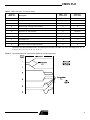
In accordance with the standards defined by the “JEDEC
STANDARD No. 3-C”, Table 1 shows some of the most
commonly used JEDEC test vector values when testing a
PLD device. The table also shows the ABEL and CUPL test
vector values that correspond to each JEDEC vector.
Test Vector Issues on the Programming
Hardware
When entering test vectors in your design, it is very important to use the proper vector values. If incorrect vector
values are used, the vectors may fail on the PLD programmer even though they passed the ABEL or CUPL functional
simulation. For instance, if you use “0” and “1” vector values to drive the clock pin of your design, the vectors will
probably fail on the programmer even though they passed
the ABEL or CUPL simulation (see Recommendation #1).
In addition to improper test vector usage, test vector failures on PLD programmers may also be a result of the
programmer’s hardware characteristics. The programming
hardware dictates the sequence in which inputs in a given
vector are applied to the device. For example, the programmer may assert “0” and “1” input vectors in a sequential
manner from the first pin to the last pin, or asserts the input
vectors almost simultaneously. In addition, the programmer
also sets the “transition” or “edge” rate of the input signals.
Most of today’s PLD programmers can drive both slow and
fast edge signals because they contain both normal and
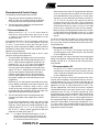
high-speed (or “clock”) input drivers. Figure 1 shows the
typical waveforms of the input signals applied by a
programmer.
CMOS PLD
Table 1. ABEL and CUPL Test Vector Values
Vector In
JEDEC File
Note:
Description
ABEL(1) Test
Vector Value
CUPL Test
Vector Value
0
Drive Pin Low
0
0
1
Drive Pin Low
1
1
C
Drive Pin Low-High-Low
.C.
C
K
Drive Pin High-Low-High, Fast Transition
.K.
K
U
Drive Pin High, Fast Transition
.U.
Not Used
D
Drive Pin Low, Fast Transition
.D.
Not Used
X
Output Not Tested, Input Defined Default Level
.X.
X
F
Float Input or Output
.F.
Not Used
L
Test Output Low
0
L
H
Test Output High
1
H
Z
Test Input or Output for High Impedance
.Z.
Z
1. In ABEL, you can assign the test vector values to identifiers (in the ABEL DECLARATIONS section), and then use these
identifiers in the TEST_VECTORS section. The following is an example of the ABEL test vector value assignments: H, L, X,
Z, D, U, C, K, F = 1, 0, .X., .Z., .D., .U., .C., .K., .F.
Figure 1. Typical Waveforms of Input Vectors Applied by a PLD Programmer
3
Recommended Vector Usage
The following recommendations will ensure:
1. That your test vectors simulations results from
ABEL or CUPL are consistent with the verification
or testing results by the programming hardware;
2. That the test-vectors applied by the programmer
are not hardware dependent.
☞Recommendation #1:
Always use the “D”, “U”, “C” or “K” vector value for
clock pins or clock product terms. Do not use “0” and
“1” values to clock registers. See Example #1 in the
Appendix Section.
For registered functions, it is very important to always use
the value “D”, “U”, “C”, or “K” to clock registers. If you use
“0” and “1” input vectors to drive the clock pin of your
design, the vectors may pass the ABEL or CUPL functional
simulation but these same vectors may fail when they are
applied on the programmer.
The two problems associated with using “0” and “1” input
values for clocking the registers are:
1. The input data to the register may not set-up prior to
the clock signal. With all PLD programmers, the “0”
and “1” input values are applied to the device’s pin
before the “D”, “U”, “C” or “K” input. This implementation ensures that the input data to the registers
are set-up prior to the registers receiving the clock
signal. If “0” and “1” input values are used for clocking, then the registers could get the clock signal
before the input data is set-up. This would cause
incorrect input signals to be set-up and clocked into
the register, resulting in a test vector failure on the
programmer.
Note that you can eliminate the input data set-up problem by adding a wait-state vector prior to each “0” and
“1” edge transition. However, using “0” and “1” input
vectors to drive the clock for the registers is still not recommended due the possibility of the slow edge rate
input drivers being used by the programmer.
2. The slow transitions of the clock signals that may
cause the input data to the register to be “double
clocked”.
In most PLD programmers, there are clock or high
speed drivers that can drive input signals with fast
edge rate. These drivers are usually dedicated for driving pins with the “D”, “U”, “C”, or “K” clock values. For
the “0” and “1” values, normal input drivers with slow
edge rate are used (see Figure 1)(1).
Note:
4
1. The JEDEC standard specifies that the “0” and “1”
vectors must use a fine current drive since the programmer must allow the applied input conditions to
be overridden by bidirectional I/O pins.
CMOS PLD
Note that there are some PLD programmers that have
clock or high speed drivers which are hard-wired to
some dedicated pins only (usually pin 1 of each package type). So, even when the clock values such as “D”,
“U”, “C” and “K” are used, test vectors may still fail
because slow drivers are used. This is especially
important for the Atmel V-Series CPLDs because the
architectures allow any input or I/O pin, or an AND
function to be configured as clock for the registers.
Many of today’s PLD programmers either have a clock
or high-speed driver dedicated to each pin, or allow
limited number of high speed drivers to be routed to
any pin.
For driving clocks that are gated in a clock product term,
the “C” or “K” value can still be used as long as the clock
pin is not used in other combinatorial functions (see Recommendation #3).
☞Recommendation #2:
Use the “D” or “U” value if your design uses the rising
and falling edges of the same clock pin. See Example
#1 in the Appendix Section.
In some designs, you may be required to use the rising and
falling clock edges to completely test the logic. With these
designs, use the “D” or “U” values on the clock pins whenever possible.
☞Recommendation #3:
Use the “D” or “U” value for generated clocks that are
implemented in product term clock functions and are
used in separate combinatorial functions. See Example
#1 in the Appendix Section.
If a clock pin is used to drive both a product term clock
function and a separate combinatorial function, then it is
recommended to use “D” or “U” value on the clock pin. As
mentioned in Recommendation #1, the PLD programmer
applies the “D” and “U” values after all the “0” and “1” values are implemented. If the clock pin is used in a separate
combinatorial function, the logic values 0 and 1 are also
asserted by the “D” and “U” values respectively. Even
though these logic values are applied a little later than the
signals implemented via the “0” and “1” values, there is still
sufficient time (typically in ms for most programmers) for
the combinatorial logic to settle out before the programmer
senses the output signal. For this type of design, the “C” or
“K” clock vector is not suitable because the clock pulse
may return to the inactive level (LOW or HIGH) before the
programmer senses the output.
CMOS PLD
☞Recommendation #4:
Do not use the “F” vector on unused inputs and I/O’s
To reduce noise being injected into the device, do not use
the “F” value because some programmers may actually
“float” the pins. We recommend that all unused device’s
inputs and I/O’s to be terminated.
☞Recommendation #5:
Use 2 to 3 vector cycles for testing bi-directional I/O’s
(See Example #7 in Appendix.)
When testing bi-directional I/O pins, it is important to specify the vectors in a proper manner. For instance, if you are
testing an I/O pin as an input, in which the I/O pin was originally configured as an output, always ensure that the I/O
pins are in high impedance state before driving them as
inputs.
When testing the I/O pin as an input (from an output
mode):
1. First, set the I/O pin to high impedance by disabling
the output enable. Use the “Z” value for the I/O pin.
2. Then, drive the I/O pin as an input.
If a single vector is used to disable and drive the I/O pins at
the same time, these I/O pins may experience signal or bus
contention conditions (i.e. the programmer is driving signals into the device’s pins, and at the same time the
device’s output pins are driving) when the vector is being
exercised on the programmer. This signal contention condition can sometimes cause your vectors to fail on the
programmer, and may possibly cause damage to the I/O
pins.
When testing the I/O pin as an output (from an input
mode):
1. Set the I/O pin to the “X” (don’t care) value.
2. Enable the output enable so that the I/O pin is
driving.
3. Set the I/O pins with values “L” and “H” (“0” and “1”
for ABEL) to verify the output signals.
5
Appendix Section - Examples on using Test-Vectors in Atmel PLDs
The following examples discuss the use of test-vectors in several different logic functions. If applicable, the test-vector
examples for each logic function are illustrated in both ABEL and CUPL HDL formats.
Example #1 - Example using the “D”, “U”, “C” and “K” vector values
The following ABEL example illustrates the usage of the “D”, “U”, “C”, and “K” clock values. Note that since the “D” and “U”
values are not supported by CUPL, the corresponding CUPL example is not shown. For illustration on the “C” and “K” clock
vectors usage in CUPL, please refer to Example #3.
DUCK.ABL
module duck
title ’ When to use .D., .U., .C., and .K. ATMEL Corporation ’;
DUCK device ’P750’;
I1,I2,I3,I4,I5
I6,I7,I8,I9,I10,I11,I13
pin
pin
1,2,3,4,5;
6,7,8,9,10,11,13;
O19,O20,O21,O22,O23
O14,O15,O16,O17,O18
pin
pin
19,20,21,22,23;
14,15,16,17,18;
B14,B15,B16,B17,B1
B19,B20,B21,B22,B23
O23
O22
node 26,27,28,29,30;
node 31,32,33,34,35;
IsType ’BUFFER,REG’;
IsType ’BUFFER,REG’;
X,Z,D,U,C,K
=.X.,.Z.,.D.,.U.,.C.,.K.;
“ Writing Test Vectors for a Asynchronous Device ”
“ If you want a complete clock cycle, use C and K on your
“ clock pins whenever possible.
“ If you want to see what happens after one clock edge, use U
“ and D on the clock pins whenever possible.
“ If you use a 1 then a 0 or a 0 then a 1 to clock your,
“ registers, then expect —- trouble.
“ Different programmers treat test vectors differently. Some go
“ from pin to pin and assert 0's and 1's in a sequential manner
“ then look for C's, K's, U's, and D's and assert them from pin
“ to pin. If 0's and 1's are used, your registers can be clocked
“ before the inputs to the registers even have a chance to change
“ and therefore the programmers report a failure to pass vector
“ message.
“ Other programmers assert 0's and 1's almost simultaneously and
“ then go through the test vector and look for C's, K's, U's, and
“ D's and then assert them almost simultaneously. This could also
“ give you a failure if you use 0's and 1's to clock. Since your
“ clock and data will be asserted almost simultaneously (still no
“ guarantee which will come first ), the set-up time is not
“ satisfied thus the programmers report a test vector failure.
“ Keep in mind that the programmers do functional tests, not timing
“ tests. It won't catch your timing errors in your design for you.
“ The test vectors simply verify your design's functionality but
“ that alone should reduce the time spent on the test bench.
Equations
O23.ck = I3;
B23.ck = !I3;
6
O23.re =
B23.re =
I6;
I6;
O23.oe =
CMOS PLD
1;
CMOS PLD
O23.D =
B23.D =
I1 # I2;
I4 & O23.Q
# I5 & !O23.Q;
O22.D = I7;
O22.ck = I8 & I9;
“I9 is clock pin used in product term and
“in O21 combinatorial function.
O21 = I9 & I10;
test_vectors (
[I1,I2,I3,I4,I5,I6]
[ 0, 0, 0, 0, 0, 1]
[ 1, 0, C, 1, 0, 0]
[ 0, 0, U, 0, 0, 0]
[ 0, 0, K, 1, 0, 0]
[ 0, 1, D, 0, 1, 0]
[ 0, 1, U, 0, 1, 0]
test_vectors (
[I7,I8,I9,I10]
[ 1, 0, U, 0 ]
[ 1, 0, D, 0 ]
[ 1, 1, U, 1 ]
[ 0, 1, D, 1 ]
[ 0, 1, U, 1 ]
end
-
-
[O23,B23])
[ 0 , 0 ];"reset
[ 1 , 1 ];"clock
[ 0 , 1 ];"clock
[ 0 , 0 ];"clock
[ 0 , 1 ];"clock
[ 1 , 1 ];"clock
O23
O23
B23
B23
O23
first then B23 - Recommendation
first then O23 - Recommendation
- Recommendation
“Recommendation #1
#2
“Recommendation #1
#2
#2
[O22,O21])
[ 0 , 0 ]; “U and D send logic 1 and 0 ”respectively
[ 0 , 0 ]; “to O21 combinatorial function.
[ 1 , 1 ]; “O21 passed - Recommendation #3
[ 1 , 0 ];
[ 0 , 1 ];
Example #2 - Testing Combinatorial Functions
The following GATES example shows how the test vectors are implemented for simple combinatorial functions such as
OR, AND, XOR and INVERT logic gates.
ABEL File
GATES.ABL
module GATES
title 'Simple examples showing how test vectors are used for combinatorial outputs';
“Inputs d0, d1
“Outputs
Out1
Out2
Out3
Out4
pin 1,2;
pin
pin
pin
pin
14
15
16
17
ISTYPE
ISTYPE
ISTYPE
ISTYPE
'COM';
'COM';
'COM';
'COM';
“Constant Declarations to be used in the TEST_VECTORS section X,H,L =
“.X. = 'Don't Care' state that can be used for inputs or outputs.
“ 1 = Logic High
“ 0 = Logic Low.
EQUATIONS
Out1 = d0 # d1;
“OR function
Out2 = d0 & d1;
“AND function
Out3 = d0 $ d1;
“XOR function
Out4 = !d0;
“INVERT function
.X.,1,0;
7
TEST_VECTORS ’Test AND/OR Functions’
([ d0, d1 ] - [ Out1 , Out2] )
[ 0 , 0 ] - [
L
,
L ];
“0 is substituted for L
[ 1 , 0 ] - [
H
,
L ];
“1 is substituted for H
[ 0 , 1 ] - [
H
,
L ];
[ 1 , 1 ] - [
H
,
H ];
TEST_VECTORS 'Test XOR/INVERT
([ d0, d1
] - [ Out3, Out4
[ 0 , 0
] - [
L
,
[ 1 , 0
] - [
H
,
[ 0 , 1
] - [
H
,
[ 1 , 1
] - [
L
,
Functions'
] )
H ];
X ];
X ];
L ];
“ABEL allows several test_vector statements to be used in a module.
“Each test vector group is compiled individually. The compiler will
“combine vectors from all groups to create a composite test vector set
“when it creates the JEDEC file.
end
CUPL Files
GATES.PLD
Name
Partno
Date
Designer
Device
GATES;
XXXXX;
3/27/95;
Atmel;
V750;
/* Inputs */
Pin 1 = d0;
Pin 2 = d1;
/* Outputs */
Pin [14..17] = [out1..4];
/* Logic Equations */
out1
out2
out3
out4
=
=
=
=
d0 # d1;
d0 & d1;
d0 $ d1;
!d0;
/*
/*
/*
/*
OR Function */
AND Function */
XOR Function */
INVERT Function */
GATES.SI
Name
Partno
Date
Designer
Device
GATES;
XXXXX;
3/27/95;
Atmel;
V750;
/****************************************************************/
/*
Simulation Input File for Gates Example
*/
/****************************************************************/
ORDER:
VECTORS:
0 1 HL HH
1 0 HL HL
8
d0,%1,d1,%1,
out1,out2,%1,out3,out4;
/* Inputs */
/* Outputs */
/* 0,1 = Input values */
/* L,H = Output values */
CMOS PLD
CMOS PLD
0
1
0
1
0
1
1
1
0
0
1
1
HL
HH
LL
HL
HL
HH
HH
LL
LH
HL
HH
LL
Example #3 - Testing Registered Functions
A simple 4 bit Binary Counter with reset function is used to illustrate the test vector implementation for a registered function.
ABEL File
COUNT4.ABL
module COUNT4
“inputs
clk
pin 1;
reset
pin 2;
“outputs
q0,q1,q2,q3 pin 14,15,16,17 ISTYPE 'REG';
“Constant Declarations to be used in the TEST_VECTORS section
C,H,L = .C.,1,0;
“.C. = Low-High-Low Clock pulse
Equations
“4-Bit Binary Counter equations using D-type registers
q0.d = !q0;
q1.d = !q1 & q0 #
q1 & !q0;
q2.d = !q2 & q1 & q0 #
q2 & !q1 #
q2 & !q0;
q3.d = !q3 & q2 & q1 & q0 #
q3 & !q2
#
q3 & !q1
#
q3 & !q0;
[q3,q2,q1,q0].ar = reset;
[q3,q2,q1,q0].clk = clk;
“resets the counter
“clocks the counter
Test_vectors '4-Bit Counter'
([clk, reset] - [q3,q2,q1,q0])
[ C ,
1 ] - [ L , L , L , L
[ C ,
0 ] - [ L , L , L , H
[ C ,
0 ] - [ L , L , H , L
[ C ,
0 ] - [ L , L , H , H
[ C ,
0 ] - [ L , H , L , L
[ C ,
0 ] - [ L , H , L , H
[ C ,
0 ] - [ L , H , H , L
[ C ,
0 ] - [ L , H , H , H
[ C ,
0 ] - [ H , L , L , L
end
];
];
];
];
];
];
];
];
];
“resets the counter
“1
“2
“3
“4
“5
“6
“7
“8
9
CUPL Files
COUNT4.PLD
Name
Partno
Date
Designer
Device
COUNT4;
XXXXX;
3/27/95;
Atmel;
V750;
/* Inputs */
Pin 1 = clk;
Pin 2 = reset;
/* Outputs */
Pin [14..17] = [q0..3];
/* Logic Equations */
/* 4-Bit Binary Counter equations using D-type registers */
q0.d = !q0;
q1.d = !q1 & q0 #
q1 & !q0;
q2.d = !q2 & q1 & q0 #
q2 & !q1 #
q2 &
!q0;
q3.d = !q3 & q2 & q1 & q0 #
q3 & !q2 #
q3 & !q1
#
q3 & !q0;
[q3..0].ar = reset;
[q3..0].ck = clk;
/* resets the counter */
/* clocks the counter */
COUNT4.SI
Name
Partno
Date
Designer
Device
COUNT4;
XXXXX;
3/27/95;
Atmel;
V750;
/****************************************************************/
/*
Simulation Input File for Register Example
*/
/****************************************************************/
ORDER: clk,%1,reset,%1,
q3, q2, q1, q0;
VECTORS:
C 1 LLLL
C 0 LLLH
C 0 LLHL
C 0 LLHH
C 0 LHLL
C 0 LHLH
C 0 LHHL
C 0 LHHH
C 0 HLLL
10
/* Inputs */
/* Outputs */
/* resets the counter */
CMOS PLD
CMOS PLD
Example #4 - Using Sets for a group of signals in Test-Vectors
When using the ABEL or CUPL design language, you can simplify the logic description for groups of signals such as
Address and Data Lines, by grouping the signals in a set. This grouping of signals in sets also simplifies your test vectors
and hence makes them easier to understand.
The 4 bit Binary Counter design from Example #3 was modified to show that the test vector implementation was simplified
by grouping the counter outputs q3, q2, q1 and q0 in a set called count. The bold words indicate either additions or
changes to the original counter design.
ABEL File
COUNT4A.ABL
module COUNT4A
“Pin declarations same as COUNT4.ABL
count = [q3,q2,q1,q0];
“Used in the TEST_VECTORS section
Equations
“Design equations same as COUNT4.ABL.
“
.
“
.
“@RADIX n
where n is 2 (binary), 8 (octal), 10 (decimal - default) or 16 (hexadecimal)
“The @RADIX compiler directive allows the base numbering system to be changed.
“The default numbering system is 10.
Test_vectors '4-Bit Counter'
([clk, reset] - count)
[ C ,
1 ] 0 ; “reset the counter
[ C ,
0 ] 1 ;
[ C ,
0 ] 2 ;
[ C ,
0 ] 3 ;
[ C ,
0 ] 4 ;
[ C ,
0 ] 5 ;
[ C ,
0 ] 6 ;
[ C ,
0 ] 7 ;
[ C ,
0 ] 8 ;
end
CUPL Files
COUNT4A.PLD
Name
/*
COUNT4A;
.
.
Design desciptions and equations same as COUNT4.PLD.
*/
field count = [q3..0];
11
COUNT4A.SI
Name
Partno
Date
Designer
Device
COUNT4A;
XXXXX;
3/27/95;
Atmel;
V750;
/****************************************************************/
/*
Simulation Input File for Register Example
*/
/****************************************************************/
Base: decimal; /* Selection: octal, decimal and hexadecimal.
This syntax sets the base numbering system.
Use single quotes for inputs, and double
quotes for outputs.
Eg. Inputs: ’9’
Outputs: “9"
If the quotes (single or double) are not used,
the default numbering system is binary, i.e. 0 or 1.
*/
ORDER: clk,%1,reset,%1,
/* Inputs */
count;
/* Outputs */
VECTORS:
C 1 “0"
C 0 “1"
C 0 “2"
C 0 “3"
C 0 “4"
C 0 “5"
C 0 “6"
C 0 “7"
C 0 “8"
Example #5 - Repeating Vectors with the ABEL @REPEAT or CUPL $REPEAT syntax
Both the ABEL and CUPL HDLs have a compiler directive that causes a vector to be repeated a specified number of times.
This REPEAT directive is particularly useful for generating sets of test vectors, especially vectors for testing counters. For
more detailed information on the syntax of the REPEAT compiler directive, please refer to your ABEL or CUPL manual.
The 4 bit Binary Counter design from Example #4 was modified further to use the REPEAT syntax. The REPEAT syntax
reduces the effort of generating the vectors for the counter design. Note that the modifications to Example #4 are indicated
by the bold words.
ABEL File
COUNT4B.ABL
module COUNT4B
“Design descriptions and equations same as COUNT4A.ABL.
“
.
“
.
@@CONST CNT = 1;
“Initialize the Constant CNT
Test_vectors '4-Bit Counter'
([clk, reset] - count)
[ C ,
1 ] 0 ; “reset the counter
[ C ,
0 ] 1 ;
12
CMOS PLD
CMOS PLD
@@REAPEAT 13 {
@@CONST CNT = CNT + 1;
[ C ,
0 ] - CNT;
“Repeat vector for 13 times
“Increment CNT
“The compiler automatically inserts the CNT value
”into the vector.
}
[ C ,
[ C ,
0
0
] ] -
15 ;
0 ;
“Last count
“Count roll back to zero
end
CUPL Files
COUNT4B.PLD
Name
/*
COUNT4B;
.
.
Design desciptions and equations same as COUNT4A.PLD.
.
*/
COUNT4B.SI
Name
Partno
Date
Designer
Device
COUNT4B;
XXXXX;
3/27/95;
Atmel;
V750;
/****************************************************************/
/*
Simulation Input File for Register Example
/****************************************************************/
Base: decimal;
*/
/* Selection: octal, decimal and hexadecimal.
This syntax sets the base numbering system.
Use single quotes for inputs, and double
quotes for outputs. Eg. Inputs: '9'
Outputs: “9" '
If the quotes (single or double) are not used,
the default numbering system is binary, i.e. 0 or 1.
*/
ORDER: clk,%1,reset,%1,
count;
VECTORS:
C 1 “0"
C 0 “1"
$REPEAT 13;
C 0 “*”
C 0 “15"
C 0 “0"
/* Inputs */
/* Outputs */
/* Repeat 13 times */
/* Last count */
/* Count roll back to zero */
13
Example #6 - Simulating Buried Nodes
In addition to output pins, ABEL and CUPL allow buried nodes (combinatorial or registered) to be simulated. Simulating the
buried logic allows the designers to debug the complex logic and state machines in their PLD designs. There are no special
requirements for simulating the buried nodes, except that it is important to note that the buried node vectors cannot be
functionally verified on a programmer. This means that the expected output for the buried nodes will not appear on the
JEDEC file. If verifying the functionality of the buried nodes on the programmer is important, then these nodes can be buffered to the unused I/O pins of the device.
☞ If a fitter is used for the Atmel-ABEL or Data I/O’s ABEL tool, the fitter will optimize the design by choosing the reversed
polarity of the combinatorial nodes (indicated by the “Polarity is INVERT” message in the fitter output file “.FIT”). To compensate for the reversed polarity, the fitter inverts all the references to the combinatorial nodes. Hence, the resulting logic
at the output pins is equivalent to the original equations. If these buried combinatorial nodes are simulated (via the “Simulate Fitted Design” or “Simulate JEDEC” command only), the vectors for these nodes will need to be inverted to reflect the
change in polarity of the buried nodes. A 4 Bit Loadable Shift Register design is used to illustrate the buried node
simulation.
ABEL File
SHIFT4.ABL
MODULE shift4
TITLE ’4-Bit Loadable Shift Register’;
“Block Diagram ”
“
“
“
“
“
“
“
“
“
“
“
“
“
“When Load is TRUE, D0..D3 data is loaded into the shift register.
“Once Load is FALSE, the data is shifted to the right (D3 - D0).
“A '0' is loaded into the D3 during the shifting process. The
“last bit of the shift register, Ser_out shifts the data out.
shift4 device 'p750';
“Inputs
CLK pin 1;
Load pin 2;
RES pin 3;
D0,D1,D2,D3 pin 4,5,6,7;
“Outputs
Ser_out pin 23 istype 'buffer,reg_d';
14
CMOS PLD
“This output is the Q0 bit.
CMOS PLD
“Q Nodes (used the ATV750 buried nodes)
Q0 = Ser_out;
Q1,Q2,Q3 node 26,27,28 istype 'buffer,reg_d';
Qnodes = [Q3,Q2,Q1,Q0];
Qshift = [0 ,Q3,Q2,Q1];
Din
= [D3,D2,D1,D0];
“Q nodes
“Shifting input, always shift 0 into Q3.
“Data input
EQUATIONS
Qnodes.clk = CLK;
Qnodes.ar = RES;
“Clock for the Shift Register
“Reset for the Shift Register
Qnodes.d =
Load & Din
# !Load & Qshift;
“Load in the data
“Shifts the data
DECLARATIONS
C,X = .C.,.X.;
@@radix 2; “set to Binary numbering system
TEST_VECTORS
([CLK, RES, Load,
[ 0 ,
0
,
[ C ,
0
,
[ C ,
0
,
[ C ,
0
,
[ C ,
0
,
[ C ,
0
,
[ C ,
0
,
[ 0 ,
1
,
end
Din] - [Qnodes,Ser_out]);
0
, X
] - [ 0000 ,
1 ,1110]
- [ 1110 ,
0 , X
] - [ 0111 ,
0 , X
] - [ 0011 ,
0 , X
] - [ 0001 ,
0 , X
] - [ 0000 ,
1 ,0101]
- [ 0101 ,
0 , X
] - [ 0000 ,
“Ser_out=Q0
0
0
1
1
1
0
1
0
];
];
];
];
];
];
];
];
“Loads Data Din
“Loads Data Din
“Resets Registers
15
CUPL Files
SHIFT4.PLD
Name
Partno
Date
Designer
Company
Assembly
Location
Device
SHIFT4;
XXXXX;
3/27/95;
PLD Expert;
Atmel;
None;
None;
V750;
/*
Block Diagram
“
“
“
“
“
“
“
“
“
“
“
“
“
When Load is TRUE, D0..D3 data is loaded into the shift register.
Once Load is FALSE, the data is shifted to the right (D3 - D0).
A '0' is loaded into the D3 during the shifting process. The
last bit of the shift register, Ser_out shifts the data out.
*/
Pin 1 = CLK;
Pin 2 = Load;
Pin 3 = RES;
Pin [4..7] = [D0..3];
/* Outputs */
Pin 23 = Ser_out;
/* This output is the Q0 bit. */
/* Q Nodes (used the ATV750 buried nodes) */
Q0 = Ser_out;
Pinnode [26..28] = [Q1..3];
16
field Qnodes = [Q3..0];
field Qshift = ['b'0,Q3..1];
field Din
= [D3..0];
/* Q nodes */
/* Shifting input, always shift 0 into Q3. */
/* Data input */
Qnodes.ck = CLK;
Qnodes.ar = RES;
/* Clock for the Shift Register */
/* Reset for the Shift Register */
Qnodes.d =
Load & Din
# !Load & Qshift;
/* Load in the data */
/* Shifts the data */
CMOS PLD
CMOS PLD
SHIFT4.SI
Name
Partno
Date
Designer
Company
Assembly
Location
Device
SHIFT4;
XXXXX;
3/27/95;
PLD Expert;
Atmel;
None;
None;
V750;
/****************************************************************/
/*
Simulation Input File for Buried Node Example
*/
/****************************************************************/
ORDER:
CLK,%1,RES,%1,Load,%1,Din,%2,
Qnodes,%2,
Ser_out=Q0 */
Ser_out;
VECTORS:
0 0 0 XXXX
C 0 1 1110
C 0 0 XXXX
C 0 0 XXXX
C 0 0 XXXX
C 0 0 XXXX
C 0 1 0101
0 1 0 XXXX
LLLL
HHHL
LHHH
LLHH
LLLH
LLLL
LHLH
LLLL
L
L
H
H
H
L
H
L
/* Inputs */
/* Buried Nodes,
/* Output */
/* Loads Data Din */
/* Loads Data Din */
/* Resets Registers */
Example #7 - Testing Bi-Directional I/O pins
The following example illustrates the use of test vectors to verify bi-directional I/O pins. It is important to specify your bidirectional I/O vectors in the following manner:
When testing the I/O pin as an input (from an output mode):
1. First, set the I/O pin to high impedance by disabling the output enable. Use the “Z” value for the I/O pin.
2. Then, drive the I/O pin as an input.
When testing the I/O pin as an output (from an input mode):
1. Set the I/O pin to the “X” (don’t care) value.
2. Enable the output enable so that the I/O pin is driving.
3. Set the I/O pins with values “L” and “H” (“0” and “1” for ABEL) to verify the output signals.
ABEL File
BIDIR.ABL
module BIDIR
Title ’This example shows how to test a bi-directional I/O pin in ABEL ’
“Inputs
ENA pin 2;
D1 pin 3;
“Output enable
17
“Outputs
IO1
IO2
pin 22 istype 'com';
pin 21 istype 'com';
“This pin is being used bi-directionally
“This pin is defined as an output
“IO1 and IO2 pins could also be defined as registered outputs
Declarations
X,Z,H,L = .X.,.Z.,1,0;
“.Z. = High Impedance or Tri-state
Equations
IO1 = D1;
IO1.oe = ENA;
“I/O pin IO1 as an output
“When ENA=1, output IO1 is enabled,
“When ENA=0, output IO1 is tristated and can be used as input
IO2 = IO1;
“IO1 is used as an input for this output
test_vectors 'Bi-directional I/O test'
([ENA, D1, IO1] - [IO1,IO2]);
“IO1 must be specified on both the input and output sides.
[ 1
,
0,
X ] - [ 0 , 0 ];
“IO1 output is enabled, it is important to use X (don't care)
“for IO1 on the input side when IO1 output is enabled. Almost
“all programmers do not drive the pins with vector X.
“Even if ENA=0 (IO1 output disabled), it is recommended to
“always use vector X on the input side of all bi-directional I/Os
“for the first vector (because the programmer may enable the
“output while setting up for the vector testing).
[ 1
,
1,
X ] - [ 1 , 1 ];
"IO2 output follows the IO1 because of the combinatorial
“feedback.
[ 0
,
0,
X ] - [ Z , 1 ];
"Disable the IO1 output, but keep the vector X on input IO1
“to ensure that it is not driven as input.
[ 0
,
0,
1 ] - [ Z , 1 ];
"It is safe to drive IO1 as an input now.
[ 0
,
0,
0 ] - [ Z , 0 ];
end
CUPL Files
BIDIR.PLD
Name
Partno
Date
Designer
Device
BIDIR;
xxxxx;
3/7/95;
Atmel;
V750;
/***************************************************************/
/* This example shows how to define and use a
*/
/* a bi-directional I/O pin in CUPL.
*/
/***************************************************************/
/* Inputs */
Pin 2 = ENA;
Pin 3 = D1;
18
CMOS PLD
CMOS PLD
/* Outputs */
Pin 22 = IO1;
Pin 21 = IO2;
/* Logic Equations */
IO1 = D1;
IO1.oe = ENA;
/* IO1 output is enabled when ENA = 1 */
IO2 = IO1.IO;
/* IO1 is used as in input here */
BIDIR.SI
Name
Partno
Date
Designer
Device
BIDIR;
xxxxx;
3/7/95;
Atmel;
V750;
/*******************************************************/
/* Simulation Input file for Bi-directional I/O
*/
/*
Example
*/
/*******************************************************/
ORDER: ENA,%1,D1,%2,
IO1,%1,IO2;
VECTORS:
0 0 Z X
1 0
1 1
0 0
L L
H H
Z X
0 0
0 0
1 H
0 L
/* Inputs */
/* Outputs */
/* Disable the I/O output pin on the first vector to ensure
no signal contentions on the programmer during
test-vector setup */
/* IO1 output is enabled and can be tested now */
/* IO2 follows the IO1 because of combinatorial feedback */
/* IO1 output is disabled. Always use a separate vector to disable the I/O
pin first */
/* IO1 is now used as an input. */
/* IO1 is now used as an input. */
Summary
The ABEL and CUPL test vectors are useful for checking the logic of your complex PLD designs through software simulation. To further verify your designs, the test vectors can be used on the PLD programming hardware to test the actual
device operation. To achieve consistent results between the software simulations and vector testing implemented on the
programmers, it is recommended that you use appropriate input and output vector values. Remember that both software
simulation and programmer vector testing provide only functional testing of your design. They are not intended to verify timing requirements of your designs.
19
Atmel Headquarters
Atmel Operations
Corporate Headquarters
Atmel Colorado Springs
2325 Orchard Parkway
San Jose, CA 95131
TEL (408) 441-0311
FAX (408) 487-2600
Europe
1150 E. Cheyenne Mtn. Blvd.
Colorado Springs, CO 80906
TEL (719) 576-3300
FAX (719) 540-1759
Atmel Rousset
Atmel U.K., Ltd.
Coliseum Business Centre
Riverside Way
Camberley, Surrey GU15 3YL
England
TEL (44) 1276-686-677
FAX (44) 1276-686-697
Zone Industrielle
13106 Rousset Cedex
France
TEL (33) 4-4253-6000
FAX (33) 4-4253-6001
Asia
Atmel Asia, Ltd.
Room 1219
Chinachem Golden Plaza
77 Mody Road Tsimhatsui
East Kowloon
Hong Kong
TEL (852) 2721-9778
FAX (852) 2722-1369
Japan
Atmel Japan K.K.
9F, Tonetsu Shinkawa Bldg.
1-24-8 Shinkawa
Chuo-ku, Tokyo 104-0033
Japan
TEL (81) 3-3523-3551
FAX (81) 3-3523-7581
Fax-on-Demand
North America:
1-(800) 292-8635
International:
1-(408) 441-0732
e-mail
[email protected]
Web Site
http://www.atmel.com
BBS
1-(408) 436-4309
© Atmel Corporation 1999.
Atmel Corporation makes no warranty for the use of its products, other than those expressly contained in the Company’s standard warranty which is detailed in Atmel’s Terms and Conditions located on the Company’s web site. The Company assumes no responsibility for
any errors which may appear in this document, reserves the right to change devices or specifications detailed herein at any time without
notice, and does not make any commitment to update the information contained herein. No licenses to patents or other intellectual property of Atmel are granted by the Company in connection with the sale of Atmel products, expressly or by implication. Atmel’s products are
not authorized for use as critical components in life support devices or systems.
Marks bearing
®
and/or
™
are registered trademarks and trademarks of Atmel Corporation.
Terms and product names in this document may be trademarks of others.
Printed on recycled paper.
0479C–09/99/xM