1
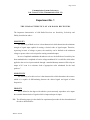
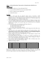
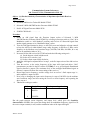
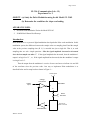
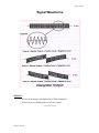
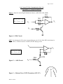
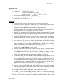
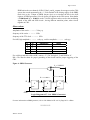
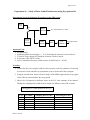
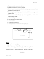
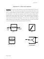
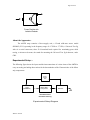
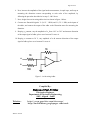
Page 1 of 28
Department of Electronics Engineering,
Communication Systems Laboratory
Laboratory Manual for EL-394
B. Tech. (Electronics), III Year (VI – Semester)
Lab Course EL 394 ( Communication Lab. – II)
LIST OF EXPERIMENTS
1. Sensitivity / Selectivity Characteristics of AM Radio Receiver (Scientech Model ST-2202)
2. Study of Delta Modulation using Scientech kit “ST-2105”
3. Experimental verification of Digital Modulation Schemes (ASK/PSK/OOK/APSK)
4. Study of Inter-symbol Interference using Eye-pattern kit
5. To plot the radiation patterns for various antennae using the ATS-2000 kit. Calculate the
directivity, beam-width and the gain for all antennae used.
6. Study of Micro-strip LPF, BPF, BRF & Power divider using the SICO AMTK-100 kit.
7. Study of Error detection and correction using 7, 4 Block codes kit.
8. Measurement of distortion using Distortion meter. Model HM 5027 (Scientific)
-----------------
Compiled by
M. Hadi Ali Khan
B. Sc. Engg (AMU)., Ex-MIEEE (USA), Ex-MIETE (India), Ex-MSSI (India)
Electronics Engineer,
Department of Electronics Engineering,
AMU, Aligarh – 202 002
Email:- m h a d ia l i k h a n @a o l .i n
Note:- This laboratory manual can also be downloaded from the following Website :-
http://www.geocities. com/elecsengr/
MHAK / 240208
Page 2 of 28
Communication Systems Laboratory
Lab. Course EL 394 (Communication Lab – II)
Experiment No. 1
THE CHARACTERISTICS OF AM RADIO RECEIVERS
The important characteristics of AM Radio Receivers are Sensitivity, Selectivity and
fidelity described as under:-
SENSITIVITY
The sensitivity of Radio receiver is that characteristic which determines the minimum
strength of signal input capable of causing a desired value of signal output. Therefore,
expressing in terms of voltage or power, the sensitivity can be defined as the minimum
voltage or power at the receiver input for causing a standard output.
In case of amplitude-modulation broadcast receivers, the definition of sensitivity has
been standardized as “amplitude of carrier voltage modulated 30 % at 400 Hz, which when
applied to the receiver input terminals through a standard dummy antenna will develop an
output of 0.5 watt in a resistance load of appropriate value substituted for the loud
speakers.”
SELECTIVITY
The selectivity of a radio receiver is that characteristic which determines the extent to
which it is capable of differentiating between the desired signal and signal of other
frequencies.
FIDELITY
This is defined as the degree with which a system accurately reproduces at its output
the essential characteristics of signals which is impressed upon its input.
NB:- The following pages give the details for experimental procedure for the determination of
the above characteristics..
MHAK / 240208
Page 3 of 28
Object:- (a) Plot the Selectitivity Characteristics of Superhetrodyne Radio Receiver.
Apparatus Used:1.
Scientech AM Receiver Trainer Kit Model ST2202
2.
Scientech 2 MHz AM/FM/Function Generator Model ST4062
3.
Pacific AF Signal Generator Model FG18
4.
20 MHz CRO Model ………….
Procedure:1.
2.
3.
4.
5.
6.
7.
8.
9.
Obtain an AM signal from the Function Output socket of Scientech 2 MHz
AM/FM/Function Generator Model ST4062 by selecting its function switch to “Sine” & its
Modulation switch to “AM Standard” positions and feed an AF Sinusoidal signal from
another signal generator to its “Modulation Input” socket.
View the AM signal obtained as above, on the CRO screen and adjust the relevant controls
to keep the AM Level within 800 mV range, audio frequency in 400 Hz to 2 KHz, carrier
frequency in the Medium wave broadcast range (say at 900 KHz) and set its modulation
index to 30 %.
Now turn ON the AM receiver and make the following setting on it:(a) Set the detector switch in diode mode.
(b) Set the AGC switch to “out”
(c) Set the volume control fully clockwise
Apply the AM signal as adjusted above in step 2, to the Rx input socket of the AM receiver
ST2202.
Tune the receiver to the carrier frequency of the input AM signal and adjust “Gain”
potentiometer provided in the RF section of ST2202 so as to get unclipped demodulated
signal at detector’s output. (The maximum level of the unclipped demodulated signal at
detector’s output will ensure the correct tuning of the receiver.)
Note the voltage level at receiver’s final output stage i.e., audio amplifier’s output on CRO
(this is the voltage at resonance, VR).
Now gradually offset the carrier frequency in suitable steps of 5 KHz or 10 KHz below and
above the carrier frequency adjusted in step 2 above, without changing the tuning of
receiver while maintaining the input signal level constant.
Now record the signal at audio amplifier’s output on CRO for different input carrier
frequencies (this is the voltage OFF-resonance, VOFF).
Tabulate the readings as under:S. No.
Carrier Frequency
Output voltage
Ratio = 20log10(VR / VOFF) dB
Plot the curve between the ratio and the carrier frequency, which gives the selectivity
characteristics of SHRR. Also record the settings done for modulation frequency, signal level at
the receiver input terminal (in mV) and the modulation index of the input AM signal.
MHAK / 240208
Page 4 of 28
Communication Systems Laboratory
Lab. Course EL 394 (Communication Lab – II)
Object:- (b) Plot the Sensitivity Characteristics of Superhetrodyne Radio Receiver.
Apparatus Used:1.
Scientech AM Receiver Trainer Kit Model ST2202
2.
Scientech 2 MHz AM/FM/Function Generator Model ST4062
3.
Pacific AF Signal Generator Model PG18
4.
20 MHz CRO Model ……………..
Procedure:1.
2.
3.
4.
5.
6.
7.
8.
Obtain an AM signal from the Function Output socket of Scientech 2 MHz
AM/FM/Function Generator Model ST4062 by selecting its function switch to “Sine” & its
Modulation switch to “AM Standard” positions and feed an AF Sinusoidal signal from
another signal generator to its “Modulation Input” socket.
View the AM signal obtained as above, on the CRO screen and adjust the relevant controls
to keep the AM Level within 800mV range, audio frequency in 400 Hz to 2 KHz, carrier
frequency in the Medium wave broadcast range (700 KHz, 800 KHz, 900 KHz, & so on)
and set its modulation index to 30 %.
Now turn ON the AM receiver kit ST2202 and make the following setting on it:(a) Set the detector switch in diode mode.
(b) Set the AGC switch to “out”
(c) Set the volume control fully clockwise
Apply the AM signal as adjusted above in step 2, to the Rx input socket of the AM receiver
ST2202.
Tune the receiver to the carrier frequency of the input AM signal and adjust “Gain”
potentiometer provided in the RF section of ST2202 so as to get unclipped demodulated
signal at detector’s output. (The maximum level of the unclipped demodulated signal at
detector’s output will ensure the correct tuning of the receiver.)
Record input carrier frequency, and the voltage level at receiver’s final output stage i.e.,
audio amplifier’s output on CRO.
Now, keep on changing the input carrier frequency in steps of 100 KHz (in the mediumwave broadcast range) and also tuning the receiver to that frequency and repeating the
above step at 6.
Tabulate the readings as under:S. No.
1
2
9
Carrier Frequency
700 KHz
800 KHz
Rx Output voltage Level
1500 KHz
Plot the graph between carrier frequency and output level, which gives the Sensitivity
characteristics of SHRR. Also record the settings done for modulation frequency, signal level at
the receiver input terminal (in mV) and the modulation index of the input AM signal.
MHAK / 240208
Page 5 of 28
EL 394 (Communication Lab – II)
Experiment No. 2
OBJECT:- (a) Study the Delta Modulation using the kit Model ST- 2105.
(b) Determine the conditions for slope-overloading.
APPARATUS USED:1.
Scientech Delta Modulation Trainer kit Model ST-2105
2.
20 MHz Dual Channel Oscilloscope
Introduction
Delta Modulation is a system of digital modulation developed after Pulse-code modulation. In this
modulation system, the difference between the sample value at a sampling time K and the sample
value at the previous sampling time (K -1) is encoded into just a single bit. That is, at each
sampling time we ask a simple question:- “Has the signal amplitude increased or decreased
since the last sample was taken ?” If the signal amplitude has increased, then the modulator’s
output is at logic level ‘1’, or, If the signal amplitude has decreased, then the modulator’s output
is at logic level ‘0’.
Thus the output from the modulator is a series of zeroes and ones to indicate rise and fall
of the waveform since the previous value. One way to implement Delta modulation is as
described below and its setup has been shown in Figure 1 :Clock Input
Voltage
Comparator
Analog
Input
CLK
BISTABLE
+
D
Q
DATA
OUTPUT
Unipolar-toBipolar Converter
INTEGRATOR
MHAK / 240208
Page 6 of 28
MHAK / 240208
Page 7 of 28
The analog signal which is to be encoded into digital data, is applied to the positive input
of the voltage comparator which compares it with the signal applied to its negative input from the
integrator output. the comparator's output is logic '0' or '1' depending upon whether the input
signal at +ve terminal is lower or greater than the negative terminal's input signal. The
comparator’s output is then latched into a D-flip-flop, which is clocked by the transmitter clock.
This binary data stream is transmitted to receiver and is also fed to the Unipolar - to - bipolar
converter which converts logic '0' to voltage level of +4V and logic '1' to voltage level of -4V.
The bipolar output is then applied to the integrator whose output is the rising linear ramp
when -4V is applied to it (corresponding to binary 1); and it is falling linear ramp when +4V is
applied to it (corresponding to binary 0). The integrator's output is fed to the negative terminal of
voltage comparator, thus completing the modulator circuit.
PROCEDURE:1.
Connect the board as shown in the diagram 1
2.
Ensure that the clock frequency selector block switches A & B are in A=0 and B=0
position.
3.
Ensure that integrator 1 block’s switches are in following position:
(A) Gain control switch in left-hand position (towards switch A & B).
(B) Switches A & B in A=0 and B=0 positions.
4.
Ensure that the switches in integrator 2 block are in following position:
(a) Gain control switch in left-hand position (towards switch A & B)
(b) Switches A & B are in A = 0 and B = 0 positions.
5.
Turn ‘ON’ of the trainer, see that the power supply LED glows. In order to ensure for
correct operation of the system, we first take the input to 0V. So connect the ‘+’ input of the
VOLTAGE COMPARATOR to 0V, and monitor on an Oscilloscope the output of
Integrator 1 (t.p.17) and the output of the transmitter’s LEVEL CHANGER (t.p15). If the
Transmitter’s LEVEL CHANGER output has equal positive and negative output levels,
INTEGRATOR’S output will be a triangle wave centered around ‘0’ volts, as shown in Fig.
1. (Case A). However, if the level changer’s negative level is greater than the positive level,
the integrator’s output will appear as shown in Fig. 5 (Case B). Should the level changer’s
positive output level be the greater of the two levels, the integrator’s output will resemble
that shown in Fig. 5 (Case C). The relative amplitude of the level changer’s positive and
negative output levels can be varied by adjusting the LEVEL ADJUST present in the
BISTABLE AND LEVEL CHANGER CIRCUIT 1 block when it is turned anticlockwise,
MHAK / 240208
Page 8 of 28
the negative level increase relative to the positive level, when turned clockwise, the positive
level increases level to the negative.
Prove that you can obtain all the three waveforms
shown in Fig.1 by turning the potentiometer from one extreme to another. Try explaining
the reason behind it.
6.
Adjust the transmitter’s LEVEL CHANGER preset until the output of INTEGRATOR 1
(t.p. 17) is a triangle wave centered around 0 Volts, as shown in Fig. 5 (Case A). The peakto-peak amplitude of the triangle wave at the integrator’s output should be 0.5V (approx),
this amplitude is known as the integrator STEP SIZE. The output from the Transmitter’s
BISTABLE Circuit (t.p. 14) will now be a stream of alternate ‘1’ and ‘0’ ‘s’, this is also the
output of the delta modulator itself. The Delta Modulator is now said to be ‘balanced’ for
correct operation.
7.
Examine the signal at the output of INTEGRATOR 2 (T.P. 47) AT THE RECEIVER. This
should be a triangle wave, with step size equal to that of INTEGRATOR 1, and ideally
centered around 0 volts. If there is any DC bias at the output of INTEGRATOR 2, remove it
by adjusting the receiver’s LEVEL ADJUST preset (in the BISTABLE & LEVEL
CHANGER CIRCUIT 2 block). This preset adjusts the relative amplitudes if the positive
and negative output levels from the receiver’s LEVEL CHANGER circuit only when these
levels are balanced and there will be no offset at the output of INTEGRATOR 2. The
receiver’s LOW PASS FILTER (Whose Cut off frequency is 3.4 KHz.) then filters output
the higher – frequency triangle wave, to level a DC level at the filter’s output (t.p. 51). If the
receiver’s LEVEL ADJUST present has been adjusted correctly, this DC level will be ‘0’
volts, the Delta demodulator are now also balanced for correct operation.
8.
Disconnect the voltage comparator’s ‘+’ input from 0V, and reconnect it to the ~ 250HZ
output from the FUNCTION GENERATOR block; the modulator’s analog input signal is
now a 250HZ sine wave. Monitor this analog signal at the VOLTAGE COMPARATOR’S
‘+’ input (t.p.9); Trigger the scope on this signal together with the output of INTEGRATOR
1 (T.P. 17) Note how the output of the transmitter’ integrator follows the analog input, as
was illustrated in Fig. 1.
Note:- It may be necessary to readjust slightly the transmitter’s LEVEL ADJUST preset (in the
BISTABLE & LEVEL CHANGER CIRCUIT 1 block) in order to obtain a stable, repeatable trace
of the integrator’s output signal.
9.
Display the data of the transmitter’s BISTABLE (at t.p. 14), together with the analog input
at t.p.9 (again trigger on this signal), and note that the 250Hz sine wave has effectively been
MHAK / 240208
Page 9 of 28
encoded into a stream of data bits at the bistable’s output, ready for transmission to the
receiver.
10. For a full understanding of how the Delta Modulator is working, examine the output of the
VOLTAGE COMPARATOR (t.p. 11), the BISTABLE’S CLOCK INPUT (t.p. 13), and the
LEVEL CHANGER’S BIPOLAR OUTPUT (t.p.15).
11. Display the output of INTEGRATION 1 (t.p. 17) and that of INTEGRATOR 2 (t.p. 47) on
the scope. Note that the two signals are very similar in appearance, showing that the
demodulator is working as expected.
12. Display the output of INTEGRATOR 2 (t.p. 47) together with the output of the Receiver’s
LOW PASS FILTER block (t.p. 51). Note that although the integrator’s output has been
smoothed out somewhat by the low pass filter, some unwanted ‘ripple’ still remains at
filter’s output. This ‘ripple’ is due to ‘quantization noise’ at the integrator’s output, which is
caused by the relatively large integrator step size. This step size can be reduced by
increasing the rate at which the system is clocked e. g. the sampling frequency), since this
reduces the sampling period, and hence the time available between samples for the
integrators to charges up and down.
13. The current system clock frequency is 32 KHz. This is set by the A, B switches in the
CLOCK FREQUENCY SELECTOR block, which are currently in the A=0, B=0 positions.
While monitoring the same signals, increase the system clock frequency to 64 KHz, by
putting the switches in the A=0, B=1 positions.
Note:- If the integrator’s output (t.p. 47) no longer gives a stable trace after changing the clock
frequency, make a slight adjustment to the transmitter’s LEVEL ADJUST preset (in the
BISTABLE & LEVEL CHANGER CIRCUIT 1 block), until the trace is once again stable. Notice
that, at the integrator’s output (t.. 47), the frequency of the triangular error signal doubles, and the
peak-to-peak amplitude of that error signal (i.e. the step size) is now halved. Examine the ripple at
the low-pass filter’s output (t.p. 51). Note that this is now less than it was before.
14. By changing the system clock frequency to first 128KHz (CLOCK FREQUENCY
SELECTOR switches in A=1, B=0 positions), and then to 256KHz (switches in A=1, B=0
positions), note the improvement in the low – pass filter’s output signal (t.p. 51). Once
again, it may be necessary to adjust slightly the transmitter’s LEVEL ADJUST preset, in
order to obtain a stable oscilloscope trace.
15. Using a system clock frequency of 256 KHz (which gives a step size of approximately 60m
V), compare the low pass filter’s output. (t.p. 51) with the original analog input (t.p. 9).
There should now be no noticeable difference between them, other than a slight delay.
MHAK / 240208
Page 10 of 28
16. While continuing to monitor the transmitter’s analog input (t.p.9) and the receiver’s lowpass filter output (t.p. 51), disconnect the comparator’s + input from the 250Hz sine wave
output, and reconnect it to the 500Hz, 1KHz and 2KHz outputs in turn. Note that, as the
frequency of the analog signal increases, the low pass filter’s output becomes more distorted
and reduced in amplitude.
17. In order to understand what has caused this distortion, leave the comparator’s + input
connected to the 2KHz sine wave output of the Function Generator, and examine the output
of INTEGRATOR 2 (T.P. 47). Note that the integrator’s output is no longer an
approximation to the analog input signal, but is instead somewhat triangular in shape.
Compare this with the output of INTEGRATOR 1 (t.p.I7), and note that the two signals are
exactly the same; the problem obviously starts in the Delta Modulator circuit.
18. Compare the 2KHz analog input signal (t.p. 9) with the output of INTEGRATOR 1 (t.p. 17)
it should now become clear what has happened. The analog signal is now changing so
quickly that the integrator's output cannot ramp fast enough to 'catch up' with it, and the
result is known as 'slope overloading.
19. Although the system clock frequency i.e. the sampling frequency determines how often the
integrator's output direction (up or down) can change, it does not affect how quickly the
integrator's output can ramp up and down. Consequently, changing the system clock
frequency will not help the slope overload problem; prove this by changing the CLOCK
FREQUENCY SELECTOR switches, and noting that the problem is still present. Return
the switches to the A = 1, B = 1 (256 KHz clock frequency) position before continuing.
20. If slope overloading is to be avoided in a practical Delta Modulation system, the transmitter
integrator must be able to ramp up or down at a rate which is at least as great as the
maximum rate of change at the transmitter’s analog input. If the incoming analog signal is a
sine wave, its maximum rate of change occurs at the zero crossing point, and is proportional
to both the frequency and the amplitude of the sine wave. Hence the likelihood of slope
overloading can be reduced by either reducing the maximum input frequency, or by
reducing the maximum input amplitude to the delta modulator. We have already seen
how slope overloading can be avoided by reducing the frequency of the analog input signal
since there was no problem with the ~ 250 Hz analog input. Now check that the problem
can also be avoided if the amplitude of the input signal is reduced. Do this by slowly turning
the ~ 2KHz preset anticlockwise. Note that there comes a time when the integrator's output
can once again follow analog input signal.
MHAK / 240208
Page 11 of 28
21. Another possible way of overcoming the slope overloading is to increase the gain of the
integrators so that they can ramp up and down faster and follow even those analog input
waveforms that change very quickly. To illustrate this, first return the ~ 2kHz preset to its
fully clockwise (maximum amplitude) position, so that slope overloading can once again be
seen on the scope. In each of the two INTEGRATOR blocks, there are two red switches
labeled A and B. The 2-bit binary code produced by these switches selects one of four
integrator gains, the lowest gain selected when the switches are in the A = 0, B = 0
positions. For each increasing step in the switch code from A = 0, B = 0 to A = l, B = l, the
integrator gain is doubled.
22. Change the codes produced by the switches (in both INTEGRATOR l and INTEGRATOR
2 blocks) from A = 0, B = 0 to A = 1, B=l, to double the gain of the two integrators; note
that slope overloading still occurs. Then change both sets of switches to the A=l, B = 0
position, and finally to the A=l, B= 1, position, to show that slope overloading can be
eliminated if the integrator gain is large enough. Once again, it may be necessary to make a
slight adjustment to the transmitter's LEVEL ADJUST pressed, in order to obtain a stable
trace on oscilloscope.
Note that, although it is the gain of INTEGRATOR 1 alone which determines whether or not
slope overloading will occur, INTEGRATOR 2 must have the same gain if the amplitude of the
Demodulator's analog output is to be equal in amplitude to the Modulator's analog input.
We have observed that the slope over loading can be overcome by changing anyone of the
following three options:(a) by reducing the maximum input frequency to the delta modulator,
(b) by reducing the maximum input amplitude, or
(c) by increasing the integrator gain.
In a practical delta modulation communications system, the signal at the modulator’s analog input
would normally be in the audio band, so that the maximum input frequency could not be reduced
below 3.4 KHz without losing information. This rules out solution (a) above.
The problem with reducing the amplitude for input signals (option b above), is that the smaller
input signals are lost in the quantization noise, they become smaller in amplitude than the
integrator’s step size.
Finally, if the integrator gain is increased (option c), the same problem results as for option (b), as
the larger step size increase quantization noise and once again ‘drowns out’ the smaller signals.
MHAK / 240208
Page 12 of 28
Signal Waveforms
REPORT:1. Discuss the advantages and applications of Delta modulation.
2. What is slope-overloading and how can it be avoided?
**************
MHAK / 240208
Page 13 of 28
Lab. Course EL 394 (Communication Lab – II)
Experiment No. 3 (Digital Modulation)
Object:- Study the various Digital Modulation Schemes (ASK, PSK, OOK, APSK)
10 K
b1 = 0, vo = + vin
b1 = 1, vo = - vin
10 K
-
Vin
Vo
+
100 K
b1
33 K
Figure 1:- PSK Circuit
OOK:- By shorting the 10 K resistor connected between pin # 2 & 6 of the PSK circuit shown in
Figure 1 above, it will now work as an OOK (ON-OFF Keying) circuit.
Vin
+
-
b2 = 0, vo = 3vin
b2 = 1, vo = vin
10 Κ
33 K
Figure 2 :- ASK Circuit
Vo
4.7 K
b2
E
Figure 3 :- Bottom View of NPN Transistor ( BC 147 )
MHAK / 240208
B C
Page 14 of 28
Apparatus Used:1. Breadboard PDC-20 (having symmetrical dual DC power supply)
2. Components:Opamps (741) = 02 nos.
NPN Transistors (BC 147) = 02 nos
Resistors :- 100K = 1, 33K = 2, 10K = 3, 4.7K = 1
3. Function Generator Model ST-4062 = 1 (for carrier)
4. Function Generator (Pacific) Model FG-18 = 1 (for TTL Clock)
5. 20 MHz Dual Trace Oscilloscope = 1
Procedure:1. Construct the PSK circuit (as shown in Figure 1 above) on the Breadboard.
2. Keeping the DC power supply OFF, connect the +15 V terminal of the supply to pin #
7, and –15 V terminal to pin # 4 of the opamp, 741, and the GND terminal to a
common point on the Breadboard, and turn ON the power supply now.
3. Obtain a sinusoidal signal from Function Generator Model ST-4062 and adjust its
amplitude around 0.5 V p-p and frequency around 8 KHz (by connecting it directly to
CRO), and connect it to the carrier input, Vin of the PSK circuit.
4. Obtain a TTL clock from the TTL output of the Function generator model FG-18, and
adjust its frequency around 6 KHz (by connecting it directly to CRO), and connect it to
modulating signal input b1 of the PSK circuit.
5. Check that all the GND terminals of both Function generators and the CRO are
connected together and are also connected to the common point made on the
Breadboard.
6. Now, connect the TTL clock to one channel, and the output of the PSK circuit to the
other channel of the CRO, and adjust the triggering and the gain controls of the CRO
properly to obtain a clear wave shape of the PSK signal on the CRO screen. Note the
shifting of the phase at every transition point of the binary TTL clock.
7. Now, short circuit the 10K resistor connected between pin 2 & 6 of opamp in the PSK
Circuit, to get an OOK signal on the CRO screen.
8. Similarly, construct the ASK circuit (as shown in Figure 2 above) on the bread board,
connect biasing power supply and connect the previously adjusted sinusoidal carrier to
the Vin input of the ASK circuit, and a TTL clock to its b2 input and display b2 on one
channel and the output, Vo of the ASK, on another channel of the CRO, and note the
shifting of the amplitudes at the transition points of the binary TTL clock.
9. To observe an APSK signal on the CRO, connect the output of the ASK to the carrier
input Vin , of the PSK, and connect b1 and b2 obtained from the PRBS generator** to
the corresponding binary inputs of ASK and PSK circuits, and display one of the b1
and b2, on one channel and the output of PSK on another channel of the CRO. Note
that APSK signal, now at the output of PSK circuit, will be appearing on CRO, whose
amplitude will be shifting in accordance with b2 and phase with b1.
10. Measure and record the high and low values of the amplitudes of the APSK signal.
11. Draw all the above signals (PSK, OOK, ASK & APSK) clearly on a graph paper and
mark the shifting of phase and amplitude of the APSK signal corresponding to b1 and
b2 from PRBS generator**.
12. Verify the truth-table for the APSK signal as shown under observations.
** To obtain b1 and b2 from the PRBS generator, connect a 5 Volts fixed DC biasing
supply to the ‘+’ & ‘-‘ inputs of the PRBS unit, and connect the previously adjusted TTL
clock (from FG-18) to the clock input of the PRBS unit, and the outputs b1 and b2 of the
MHAK / 240208
Page 15 of 28
PRBS unit to the two channels of CRO. If the b1 and b2, outputs do not appear on the CRO
screen, then touch momentarily the + 5 Volt terminal of the biasing supply of the PRBS
(Red wire) to the ‘D’input of PRBS (brown wire) (to re-circulate the bits in the shift
registers of PRBS generators). Now b1 and b2, will appear on the CRO screen. Note that b1
= 1110010 and b2 = 1100101, are the 7-bit PN sequences and are used as the modulating
signals of the ASK and PSK circuits , having different transition points, when viewed
together on CRO.
Observations
Amplitude of the carrier = -------- Volts p-p
frequency of the carrier = -------- KHz
frequency of the TTL clock = -------- KHz
For ASK, high amplitude = ------- volts p-p, and low amplitude = ------- volts p-p
b1
b2
0
0
1
1
0
1
0
1
Amplitude
phase
For verifying truth table of the APSK, connect +5 V DC for logical ‘1’ and GND for ‘0’.
NB:- Care must be taken for proper grounding of the circuits and for proper triggering of the
CRO.
Figure 4:- PRBS Generator
b3 = 1001011
b1 = 1110010
D
Q
1
CLK
D
Q
2
CLK
b2 = 1100101
D
Q
3
b3
CLK
CLK
Logic Diagram of 7 - bit PRBS Generator
For more information on PRBS generator, refer to “Lab Manual of EL 492” by Engr M. H. A Khan.
************
MHAK / 240208
Page 16 of 28
Experiment 4 :- Study of Inter Symbol Interference using Eye-pattern kit.
Experimental Set-up for displaying Eye-pattern on the CRO screen:-
EXT
Clock
EXT
Sweep
Generator
To X- input of CRO in X-Y mode
INT
Internal
Clock
Generator
PRBS
Generator
Buffer
R-C
Channel
To Y- input of CRO
Apparatus Used:1.
2.
3.
4.
5.
Eye-pattern Kit
Symmetrical Dual Power Supply (+/_ 15 V) for biasing the electronic circuits in the kit.
5-Volts DC Power Supply for biasing the electronic circuits in the kit.
A dual trace CRO with X-Y mode
An R-C channel box having a variable resistor of 10 KΩ and a C = 0.22µF
Procedure:1. Connect the DC power supplies with the correct polarity to the Eye-pattern kit for biasing
its electronic circuit and make its experimental set-up as shown in the above diagram.
2. Using the internal clock, observe the wave-shapes of the PRBS signal and the sweep signal
on the CRO screen and measure the sweep period.
3. Observe the Eye-pattern for different values of the R-C time constants of the channel.
Tabulate the sampling interval and the noise margin for different values of R, as under:Sweep period = 2x(bit-duration of one eye)
S. No.
1.
2.
3.
4.
5.
6.
MHAK / 240208
R (ohms)
Sampling Interval (ms)
Noise Margin (Volts)
Page 17 of 28
4. Find the value of R at the point where Eye closes.
5. Find the value of R when eye opening is maximum.
6. Using an inductor L with the channel, Find R for which opening is maximum and find the
maximum noise margin in this case.
7. Using the equalizer (10 KΩ preset pot.) with the channel, find the noise-margin and the
sampling interval.
8. Using the channel with R = 2KΩ (adjusted), and C = 0.22µF, (fixed), trace the boundaries
of the Eye-pattern and find :(a) space for sampling
(b) noise-margin at the best sampling instant
(c) zero-crossing jitters
(d) Distortion at the sampling time.
(e) sensitivity to timing error in the center of the sampling space
270 Ω
10 K Ω
0.22 µF
R-C Channel
Report :1.
2.
3.
4.
Discuss the results obtained.
Give the circuit details of PRBS generator.
Draw the Eye-pattern of a given binary sequence.
What will be the Eye-pattern of a M-array signal ? What is its significance?
(Reference:- Haykins, S. : “Digital Communication”. John Wiley & Sons, 1988)
***********
MHAK / 240208
Page 18 of 28
Lab. Course EL 394 (Communication Lab – II)
Experiment No. 5 (Antenna)
Object:To plot the radiation pattern of various types of directional antennae using ATS-2000 kit.
Determine the directivity, beam-width and the gain of these antennae.
Equipments Used :1. Amitec Antenna Trainer Kit, Model ATS-2000,
2. Dipole and Yagi (3-element) antennae,
3. Antenna Tripod with connecting cables, Measuring tape,
PROCEDURE:a. Connect the dipole antenna to the transmitter tripod and attenuatoe. Rotate CCW to
low RF level to avoid receiver saturation. Set the length of the antenna elements to
λ/4 or 12 cms. Each from center of the boom. Keep the antenna in horizontal
direction.
b. Now connect the Yagi antenna to the receiver tripod.
c. Set the distance between the antennae to be around 1 meter. Remove any stray
objects from around the antennae, specially in the line of sight. Avoid any
unnecessary movement while taking the readings.
d. Adjust the frequency control for maximum reading in level display.
e. Now rotate the Yagi antenna around its axis insteps of 5 or 10 automatically by
stepper motor and take the readings in receiver at each step and note down in your
observation table.
f. Plot the readings on a polar plane.
Calculations:1.
Beam width:- It is defined as the angular width in degrees at the points on either side of
the main beam where the radiated level is 3 dB lower than the maximum lobe value.
2.
From the polar plot, measure the angle where the 0 degree reference is there. This shall
also be the direction of main lobe or boresight direction.
3.
Measure the angle when this reading is -3dB on its either side.
4.
The difference between the angular positions of the -3dB points is the Azimuth plane
beam-width of the dipole antenna.
MHAK / 240208
Page 19 of 28
5.
Side lobe level is usually taken as the level below the boresight gain. Strictly all peaks
on either side of the main lobe are side lobes. However in practice only the lobes
adjacent to the boresight maxima are referred to as side lobes.
6.
Side lobes in this case shall form between the two maximas. Nulls can be upto -20dB
from the boresight direction gain.
7.
If the plot forms distinct side lobes then each one’s angular position and level can be
inferred from the plot.
8.
The front to back ratio is a measure of the ability of the directional antenna to
concentrate its beam in the required forward direction.
9.
Observe the difference in levels in dB from boresight direction and the direction
diametrically opposite to it.
10. Polarization is the shape and orientation of the focus of the extremity of the electric field
vector as it varies with time at a fixed point in space.
11. For a linear antenna like dipole, the polarization direction is the direction of its
elements.
12. Find the direction of polarization of a dipole antenna.
13. Now repeat the procedure for folded dipole antenna and find the same parameters.
Observe the difference, if any, from a simple dipole antenna.
14. Measure the elevation plane beam width of the dipole antenna from elevation plane plot.
15. Calculate the directivity as 41,000/(3dB beamwidth Azimuth planeX 3dB beamwidth
elevation plane in degrees). Take a log of this value and multiply by 10 for readings in
dBi. See that this formula is approximate and should be used judiciously.
16. Say the Azimuth plane beamwidth of dipole is 70 degrees and elevation plane
beamwidth is 300 degrees, the D = 41,000/(70X360) = 1.62, which is equal to 2.1 dBi
from relation D in dBi = 10 log D
17. As the dipole antenna is itself the reference antenna for gain measurements, hence its
absolute gain can not be directly found out. However the gain of other antennae can be
referred to dipole gain.
18. Use a jumper lead to connect the two tripods and take the reading in the receiver. If the
reading is more than 70 dB then press another attenuator. Say, the reading is 60 dBµV.
Now connect two dipole antennae at tripods with 1 meter distance between them. Say
the reading is 30 dBµV now.
19. Calculate the received power.
MHAK / 240208
Page 20 of 28
20. The accepted power is 12 nW for a reading of 60 dBµV. And received power is
0.0012 nW for a receiver reading of 30 dBµV with antenna at a distance R of 1 m at λ
of 0.5 m. We assume here that accepted power is equal to power fed to the antenna and
no reflections are being taken into account.
Results:Gain is found as = 0.8
Gain in dBi = 10 log G = 0.97 dBi
Now gain = Directivity*Efficiency, so
Efficiency of Dipole antenna is = (0.8) / (1.62) = 50 %
Repeat the experiment for folded dipole as well.
Note:The power conversion table is available in the Communication lab of the Department of
Electronics Engineering, AMU, Aligarh.
************
MHAK / 240208
Page 21 of 28
Experiment No. 6 (Micro strip Components)
Introduction:- The objective of this experiment is to get the knowledge about the Microwave
Integrated Circuits (MICs), fabricated using standard micro strip technology and available in the
form of “Advanced Micro-strip Trainer Kit (AMTK). By using this kit, the students can study
the Characteristics of some Micro strip components such as Low-pass filters, band-pass filters,
band-stop filters and the power dividers. These micro strip components have been designed to
operate in the C-band (having a center frequency = 5 GHz) and are available in the form of
printed circuit boards, which can be mounted on a “Universal Test Jig” with the help of its springloaded mechanism for the testing-purpose. The following figures show the printed circuit boards
of some of the individual micro strip components included in the AMT kit :-
Input
From
VCO
Output to
Detector
LPF
Band Stop Filter
MHAK / 240208
BPF
Power Devider without
Isolation Resistor
Page 22 of 28
Power Devider with
Isolation Resistor
About the Apparatus:The AMTK setup contains a Power-supply unit, a C-band solid-state source model
SSS980C (VCO) operating in the frequency-range of 4.7 GHz to 5.7 GHz, a Universal Test Jig
with six co-axial connectors, three 50 Ω matched loads required for terminating ports while
testing, a microwave detector, the stands for mounting the Universal Test Jig & detector, and a
CRO.
Experimental Setup :The following figure shows the layout and the interconnections of various items of the AMTK to
carry out testing and taking observations for the determination of the Characteristics of the Micro
strip components:-
Power
Supply
Unit
VCO
(SSS980C)
Micro Strip
Component
Detector
mounted on the
Universal Test Jig
Experimental Setup Diagram
MHAK / 240208
To
CRO
Page 23 of 28
Procedure: 1. Make the experimental setup as shown in figure above.
2. Insert the micro strip component to be tested into the Universal Test Jig by turning its lever
anti-clockwise and after placing the component inside the jig, again turn the lever in
clockwise direction to lock the 2”X2” substrate of the microstrip component in position. In
this position the input and output microstrip line conductors make a perfect contact with the
co-axial connector tab. The circuit is now ready for testing.
3. Now, turn ON the Power Supply Unit and adjust its voltage such that the VCO (a C-band
solid-state source model SSS980C) displays a frequency of 4.7 GHz.
4. Adjust the required controls of the CRO to display properly a signal at the output of the
detector, having the waveform like square-wave.
5. Measure the amplitude of the signal displayed on the CRO screen corresponding to the
VCO frequency of 4.7 GHz.
6. Keep on changing the VCO frequency by turning the voltage control knob of the power
supply unit and take measurements at discrete frequencies and record your observations in
the form of the table shown under the observations, and plot the characteristics (gain versus
frequency) over a specified frequency band.
7. For Power Dividers, measure the amplitudes at both the output ports.
8. Record your observations in a tabular form as shown under the heading of observations.
OBSERVATIONS:(a) For low-pass filters:-
S. No.
1.
2.
3.
4.
5.
6.
7.
MHAK / 240208
VCO frequency (GHz)
Amplitude (voltsp-p)
Page 24 of 28
Similarly, record your observations for the following microstrip components:1. Band Pass Filter (BPF),
2. Band Stop Filter (BSF),
3. Power Divider without isolation resistor
4. Power Divider with isolation resistor.
Result:- Plot the characteristics (amplitude versus frequency) over a specified frequency band
(4.7 GHz to 5.7 GHz) for the microstrip components used above.
Report:1. How can you realize Microwave Filters?
2. Discuss the applications of Microwave filters.
References:1. User Manual of Advanced Microstrip Trainer Kit.; SICO, India.
2. Matthaei, Young and Jones : Microwave Filters, Impedance Matching Networks and
Coupling Structures, Artek House, Dedhan, Mass, 1980.
3. T. C. Edwards : Foundations for Microstrip Engineering, John Wiley, New York, 1981
*************
MHAK / 240208
Page 25 of 28
Experiment N0.7
Object:- Study and experimentally verify the error detection and correction using 7, 4 Block
Code kit.
Procedure:1. Connect a 5-Volts DC Power Supply to the 7, 4 Block code kit.
2. Use the given logic probe to detect the logic levels of various bits.
3. Tabulate yours observations as shown in the following table :OBSERVATIONS:-
S. No
1.
2.
3.
4.
5.
6.
7.
8.
9.
10.
11.
12.
13.
14.
15.
16.
17.
18.
Message Bits
Transmitted
m4 m3 m2 m1
0
0
1
1
0
0
1
1
0
0
1
1
0
0
1
1
1
1
0
0
1
1
0
0
Redundant
Bits
generated
C1 C2 C3
Bits made
Erroneous
Syndrome
generated
S1
S2
S3
Output
Carry
C0
Message Bits
Recieved
m4
m3 m2
m1
None
m1
m2
m1 m2
None
m3 m4
Result:Give your remarks in each case about the detection and correction of error.
Conclusions:1. When one bit is erroneous, the output carry C0 = 0, and the error is detected and corrected.
2. When two bits are erroneous, the output carry C0 = 1, and the error is detected but it is not
corrected.
3. When three bits are erroneous, the output carry C0 = 1, and the error is neither detected and
nor corrected.
MHAK / 240208
Page 26 of 28
(Hardware Realization of 7, 4 Block Code)
(1) Generation of Redundant bits (C1, C2, C3, C4):C1 = m1 (+) m2 (+) m3
m1 m2
1 1
1= 1
1 0
__
C2 = m1 (+) m2 (+) m4
H ==
C3 = m1 (+) m3 (+) m4
m3
1
0
1
m4
0
1
1
C1 C2 C3
1 0 0
0 1 0
0 0 1
C4 = m1 (+) m2 (+) m3 (+) m4 (+) C1 (+) C2 (+) C3
= m2 (+) m3 (+) m4
(2) Introducing error in the message bits:To make m1 erroneous, connect M1 to ‘1’, otherwise connect it to ‘0’
To make m2 erroneous, connect M2 to ‘1’, otherwise connect it to ‘0’
And so on, and so forth ……
(3) Generation of Syndrome (S1, S2, S3 ) :S1 = m1/ (+) m2/ (+) m3/ (+) C1/
S2 = m1/ (+) m2/ (+) m4/ (+) C2/
S3 = m1/ (+) m3/ (+) m4/ (+) C3/
(4) Output Carry (C0) :C0 = S1 (+) S2 (+) S3) (+) g/
where g/ = m1/ (+) m2/ (+) m3/ (+) m4/ (+) C1/ (+) C2/ (+) C3/ (+) C4/
= 0
no error;
S = 0 Î C0 = 0
= 1
1 error
S = 1 Î C0 = 0
= 0
2 errors
S = 1 Î C0 = 1
(5) Received message bits :m1 = m1/ (+) A , where A = S1S2 S3
−
m2 = m2 (+) B , where B = S1S 2 S 3
/
_
m3 = m3 (+) C , where C = S1 S 2 S 3
/
_
m4 = m4 (+) D , where D = S 1 S2 S 3
/
*************
MHAK / 240208
Page 27 of 28
III Year B. Tech (Electronics)
Lab. Course EL 394 (Communication Lab)
Experiment No. 8
OBJECT :- To measure the Distortion content of the signal. Study the variation of distortion
content by changing the signal content and the noise contents of the signal using an inverter adder
circuit..
APPARATUS
1. Two signal generators,
2. An adder circuit
3. Distortion Factor Meter, Scientific Model HM 5027
4. CRO
PROCEDURE :
1. Study the specifications and function of various controls of the Distortion Factor Meter,
( Scientific Model HM 5027).
2. Apply the signal to be investigated to the Input socket (10) of HM 5027.
3. Calibrate HM 5027 by adjusting the attenuator controls (12) and the level control (3),
(within the admissible voltage range from 0.3 V to 50 V of the signal to be investigated);
the instrument HM 5027 is fully calibrated when it reads 100 %.
4. Next, carry on the frequency alignment of the instrument. During the frequency alignment,
the frequency of the integrated filter is tuned to the input signal frequency. First the
FREQUENCY RANGE push button (3) are pressed to select the required range of from
the following ranges: 20 Hz to 200 Hz, 200 Hz to 2 KHz, 2 KHz to 20 KHz. The
continuous adjustment within the selected range is performed by means of knob (6)
During the course of alignment. One of the two LEDs indicates the direction of frequency
deviation of the integrated filter with respect to the input signal; i.e., when the LED on the
right lights up, the adjustment knob must be turned counter- clockwise, until the LED goes
off, and vice versa. When both LEDs are off, the alignment procedure is completed.
5. Select the desired range of distortion by pressing the appropriate push-button (7). In case
of unknown magnitude of the distortion factor, the 100 % range should be selected first;
otherwise the display will start flashing as soon as the full deflection value of the
measurement range is exceeded. In case of insufficient resolution of the display, the next
smaller range should be selected. The distortion factor is directly read out on the display in
percent, requiring no further conversion. The read-out range extends from 99.9 % to 0.1 %
or from 9.99 % to 0.01 % respectively.
MHAK / 240208
Page 28 of 28
6. Now, increase the amplitude of the signal under measurement, in equal steps, and keep on
measuring the distortion content corresponding to each value of the amplitude, by
following the procedure described as in steps 3, 4 & 5 above.
7. Next, design & test an inverting adder circuit as shown in figure 1 below.
8. Connect two Sinusoidal signals: V1 (2.0 V / 1 KHz) and V2 (3V / 1 KHz) at the inputs of
the adder; and connect the output of the adder to the Distortion meter for measuring the
distortion.
9. Keeping v2 constant, vary the amplitude of v1 from 1.0 V to 5.0 V and measure distortion
of the output signal of adder; plot a curve between D versus A.
10. Keeping v1 constant at 3.0 V, vary amplitude of v2 & measure distortion of the output
signal of adder; plot a curve between D versus A.
1K
1K
-
v1
v2
vo
+
10K
Figure 1: An Inverting Adder
Compiled By:-
Muhammad Hadi Ali Khan
Electronics Engineer,
Department of Electronics Engineering,
AMU, Aligarh – India
Websites:-
MHAK / 240208
http:// www.geocities.com/elecsengr/
http://hadialikhan.googlepages.com/work