1
Page 1 of 26
Department of Electronics Engineering,
Communication Systems Laboratory
Laboratory Manual
for
B. Tech. (Electronics), III Year (VI – Semester)
Lab Course EL 394 ( Communication Lab. – II)
List Of Experiments for the Session 2010 – 2011
1. Selectivity Characteristics of AM Radio Receiver (Scientech model ST-2202)
2. Study of PLL Characteristics and its use as the FM Demodulator
3. Study of Optical Fiber Communication
4. Study of Micro-strip Circuits and their characteristics using AMTK-100 kit
5. Study of various Data Formats and their transmission & reception by FSK
6. Study of Digital Modulation Schemes – ASK, PSK, OOK, APSK
7. Study of TDM & PCM using Scientech kits ST-2103 & ST-2104
8. Study of Delta Modulation and condition of slope over-loading using ST-2105 kit
**************
Compiled by
Engr M. Hadi Ali Khan
B. Sc. Engg (AMU), MIETE (India), Ex-MIEEE (USA), Ex-MSSI (India)
Department of Electronics Engineering,
AMU, Aligarh – 202 002
Email:- e n g i n e e r _ a m u @ y m a i l . c o m
Note:- This laboratory manual is also available on the internet at the following URL :-
http://mhakhan.tripod.com/lab.html
http://mhakhan.tripod.com/lab.html
Page 2 of 26
Experiment No. 1
Object:- Plot the Selectitivity Characteristics of AM Radio Receiver at 1200 KHz.
Apparatus Used:1. Scientech AM Receiver Trainer Kit Model ST2202
2. Scientech 2 MHz AM/FM/Function Generator Model ST4062 (used as AM signal Generator)
3. Pacific AF Signal Generator Model FG18 (used as a message signal generator)
4. 20 MHz CRO Model ………….
Procedure:1. Obtain an AM signal from the Function Output socket of Scientech 2MHzAM/FM/ Function Generator
Model ST4062 by selecting its function switch to “Sine” & its Modulation switch to “AM Standard”
positions and feed an AF Sinusoidal signal from another signal generator to its “Modulation Input” socket.
2. View the AM signal obtained as above, on the CRO screen and adjust the relevant controls to keep the
AM Level within 800 mV range, audio frequency in 400 Hz to 2 KHz, carrier frequency in the Medium
wave broadcast range (say at 900 KHz) and set its modulation index to 30 %.
3. Now turn ON the AM receiver and make the following setting on it:(a) Set the detector switch in diode mode.
(b) Set the AGC switch to “out”
(c) Set the volume control fully clockwise
4. Apply the AM signal as adjusted above in step 2, to the Rx input socket of the AM receiver ST2202.
5. Tune the receiver to the carrier frequency of the input AM signal and adjust “Gain” potentiometer
potentiometer provided in the RF section of ST2202 so as to get unclipped demodulated signal at
detector’s output (tp38). (The maximum level of the unclipped demodulated signal at detector’s output
will ensure the correct tuning of the receiver.)
6. Note the voltage level at receiver’s final output stage i.e., audio amplifier’s output (tp39) on CRO (this
is the voltage at resonance, VR).
7. Now gradually offset the carrier frequency in suitable steps of 2 or 5 KHz below and above the carrier
frequency adjusted in step 2 above, without changing the tuning of receiver while maintaining the input
signal level constant.
8. Now record the signal at audio amplifier’s output (tp39) on CRO for different input carrier frequencies
(this is the voltage OFF-resonance, VOFF).
9. Tabulate the readings as under:- Receiver tuned to frequency, fc = 1200 KHz
S. No.
1.
2.
3.
4.
Carrier frequency of the
transmitted AM signal (KHz)
1190
1195
1200
1205
Receiver Output
(mV)
Ratio = 20log10(VR / VOFF) dB
(VR)
http://mhakhan.tripod.com/lab.html
Page 3 of 26
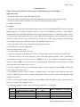
10. Plot the curve between the ratio and the carrier frequency, which gives the selectivity
characteristics of AM Radio receiver. Also record the settings made for modulation frequency,
signal level at the receiver input terminal (in mV) and the modulation index of the input AM
signal, as follws:(a) AM Level = ………………………. Volts p-p
(b) Message frequency in the AM signal = ………….. Hz
(c) Modulation index = ………….. %
(d) Carrier frequency - ………………. KHz
Selectivity Characteristics
Reference:-
1. Kennedy : Electronics Communication
2. Terman, F. E. : Electronics and Radio Engineering
3. User Manual of the kit ST-2202
4. website :- http://mhakhan.tripod.com/lab.html
************
http://mhakhan.tripod.com/lab.html
Page 4 of 26
Experiment No.2
PLL as the FM Demodulator
Object:-
(a) Determine the lock-range and the Capture-range of the given PLL kit.
(b) Plot the demodulation characteristics ( VD vs ∆f ) and verify that the given
PLL circuit is working as the Demodulator. Of the FM signal.
Apparatus Used :-
1. The PLL Kit,
2. A Function generator with digital frequency display (1 MHz)
3. A Dual Trace CRO (20 MHz)
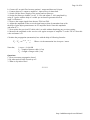
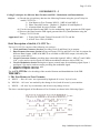
Figure 1
Figure 1 shows the experimental set-up & fig. 2 shows the Block-diagram of a PLL chip
Figure 2
http://mhakhan.tripod.com/lab.html
Page 5 of 26
Theory :- The functional characteristics of the PLL are described in the Data-sheet supplied by the
manufacturer of PLL chip NE565. Refer to the data-sheet of NE565.
Observations:-
(a) Free-running frequency, fo = ------- KHz ; (fo = 1/To, )
f1 = ………………KHz ;
( L -- UL )
f2 = ……………
KHz ;
( UL -- L )
f3 = ………………KHz ;
( L -- UL )
f4 = ………………KHz ;
( UL -- L )
(b) Lock-range (fL)
= ( f1 – f3) =
(c) Capture-range (fc) = ( f2 – f4 ) =
KHz
KHz ; (Verify that fL > fc )
(d) Readings for Demodulation Characteristics:
S. No.
Incoming signal frequency (fi)
DC Level of the
Differential output
(VD)
∆f = ( fi – fo)
Vi = a sinusoidal signal having variable frequency & amplitude around 8 volts p-p (obtained
from an external signal generator) to be connected at input of the PLL marked Vi ; for
the purpose of determination of the lock-range, capture-range & the Demodulation
characteristics of the PLL circuit.
Result:A curve between VD versus ∆f shows the Demodulation characteristics of the PLL and is linear, which
justifies that the given circuit of the PLL (NE565) is working as a demodulator of a FM signal having
maximum frequency deviation less than the lock-range of the PLL..
Report:1.
2.
Draw the circuit diagram of the PLL and give an expression for its free-running frequency.
Discuss the applications of the PLL in actual practice.
http://mhakhan.tripod.com/lab.html
Page 6 of 26
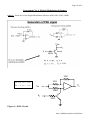
Circuit diagram of FM Demodulator using PLL NE565 / LM565
*************
http://mhakhan.tripod.com/lab.html
Page 7 of 26
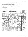
Experiment 3 : Study of Optical Fiber Communication
3(a) Objective: Setting up Fiber Optic Analog Link
Study of a 650nm fiber optic analog link in this experiment you will study the
relationship between the input signal and received signal.
Equipments Required:
1. ST2502 trainer with power supply cord
2. Optical Fibre cable
3. Cathode ray oscilloscope with necessary connecting probe
Connection diagram:-
http://mhakhan.tripod.com/lab.html
Page 8 of 26
Procedure:
1. Connect the power supply cord to the main power plug & to trainer ST2502.
2. Ensure that all switched faults are ‘Off’.
3. Make the following connections as shown in figure 1.1
a. Connect the 1 KHz sine wave output to emitter l's input.
b. Connect the Fiber Optics cable between emitter output and detectors input.
c. Detector l's output to AC amplifier 1 input.
4. On the board, switch emitter l's driver to analog mode.
5. Switch ON the power supply of trainer and oscilloscope.
6. Observe the input to emitter 1 (TP5) with the output from AC amplifier 1 (TP28)
and note that the two signals are same.
Questions:
1. What is meant by index profile?
2. What is the drawback of multimode fibres?
3. What is fibre optics?
*******
http://mhakhan.tripod.com/lab.html
Page 9 of 26
Object 3 (a) :- To measure propagation or attenuation loss in optical fiber
Equipments Required:
1. ST2502 trainer with power supply cord
2. Optical Fibre cable
3. Cathode ray oscilloscope with necessary connecting probe
Procedure:1. Connect power supply cord to the main power plug & to trainer ST2502.
2. Make the following connections as shown in the above connection diagram (on page-3).
a. Function generator’s 1 KHz sine wave output to Input 1 socket of emitter 1 circuit via 4 mm lead.
http://mhakhan.tripod.com/lab.html
Page 10 of 26
b. Connect 0.5 m optic fiber between emitter 1 output and detector l's input.
c. Connect detector 1 output to amplifier 1 input socket via 4mm lead.
3. Switch ON the Power Supply of the trainer and oscilloscope.
4. Set the Oscilloscope channel 1 to 0.5 V / Div and adjust 4 - 6 div amplitude by
using X 1 probe with the help of variable pot in function generator block at
input 1 of Emitter 1.
5. Observe the output signal from detector TP10 on CRO.
6. Adjust the amplitude of the received signal same as that of transmitted one with
the help of gain adjust potentiometer in AC amplifier block. Note this amplitude
and name it V1.
7. Now replace the previous FG cable with 1 m cable without disturbing any previous setting.
8. Measure the amplitude at the receiver side again at output of amplifier 1 socket TP 28. Note this
value end name it V2.
Calculate the propagation (attenuation) loss with the help of following formula:-
V1 / V2 = eNote that,
α (L + L )
1
2
Where α is the attenuation loss in nepers / meter
1 neper = 8. 686 dB
L1 = length of shorter cable (0.5 m)
L2 = Length of longer cable (1 m)
Questions:
1. How to measure propagation losses?
2. By what optical cable is made up of?
3. What is step index fibre?
*******
http://mhakhan.tripod.com/lab.html
Page 11 of 26
Experiment No. 4 (Micro strip Components)
Introduction:- The objective of this experiment is to get the knowledge about the Microwave
Integrated Circuits (MICs), fabricated using standard micro strip technology and available in the form
of “Advanced Micro-strip Trainer Kit (AMTK). By using this kit, the students can study the
Characteristics of some Micro strip components such as Low-pass filters, band-pass filters, band-stop
filters and the power dividers. These micro strip components have been designed to operate in the Cband (having a center frequency = 5 GHz) and are available in the form of printed circuit boards,
which can be mounted on a “Universal Test Jig” with the help of its spring-loaded mechanism for the
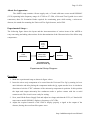
testing-purpose. The following figures show the printed circuit boards of some of the individual micro
strip components included in the AMT kit :-
Input
From
VCO
Output to
Detector
BPF
LPF
Band Stop Filter
Power Devider without
Isolation Resistor
Power Devider with
Isolation Resistor
http://mhakhan.tripod.com/lab.html
Page 12 of 26
About the Apparatus:The AMTK setup contains a Power-supply unit, a C-band solid-state source model SSS980C
(VCO) operating in the frequency-range of 4.7 GHz to 5.7 GHz, a Universal Test Jig with six co-axial
connectors, three 50 Ω matched loads required for terminating ports while testing, a microwave
detector, the stands for mounting the Universal Test Jig & detector, and a CRO.
Experimental Setup :The following figure shows the layout and the interconnections of various items of the AMTK to
carry out testing and taking observations for the determination of the Characteristics of the Micro strip
components:-
Power
Supply
Unit
VCO
(SSS980C)
Micro Strip
Component
Detector
To
CRO
mounted on the
Universal Test Jig
Experimental Setup Diagram
Procedure: 1. Make the experimental setup as shown in figure above.
2. Insert the micro strip component to be tested into the Universal Test Jig by turning its lever
anti-clockwise and after placing the component inside the jig, again turn the lever in clockwise
direction to lock the 2”X2” substrate of the microstrip component in position. In this position
the input and output microstrip line conductors make a perfect contact with the co-axial
connector tab. The circuit is now ready for testing.
3. Now, turn ON the Power Supply Unit and adjust its voltage such that the VCO (a C-band solidstate source model SSS980C) displays a frequency of 4.7 GHz.
4. Adjust the required controls of the CRO to display properly a signal at the output of the
detector, having the waveform like square-wave.
http://mhakhan.tripod.com/lab.html
Page 13 of 26
5. Measure the amplitude of the signal displayed on the CRO screen corresponding to the VCO
frequency of 4.7 GHz.
6. Keep on changing the VCO frequency by turning the voltage control knob of the power supply
unit and take measurements at discrete frequencies and record your observations in the form of
the table shown under the observations, and plot the characteristics (gain versus frequency)
over a specified frequency band.
7. For Power Dividers, measure the amplitudes at both the output ports.
8. Record your observations in a tabular form as shown under the heading of observations.
OBSERVATIONS:(a) For low-pass filters:-
S. No.
VCO frequency (GHz)
Amplitude (voltsp-p)
1.
2.
3.
4.
5.
6.
7.
Similarly, record your observations for the following microstrip components:1. Band Pass Filter (BPF),
2. Band Stop Filter (BSF),
3. Power Divider without isolation resistor
4. Power Divider with isolation resistor.
Result:- Plot the characteristics (amplitude versus frequency) over a specified frequency band (4.7
GHz to 5.7 GHz) for the microstrip components used above.
http://mhakhan.tripod.com/lab.html
Page 14 of 26
Report:1. How can you realize Microwave Filters?
2. Discuss the applications of Microwave filters.
References:1. User Manual of Advanced Microstrip Trainer Kit.; SICO, India.
2. Matthaei, Young and Jones : Microwave Filters, Impedance Matching Networks and Coupling
Structures, Artek House, Dedhan, Mass, 1980.
3. T. C. Edwards : Foundations for Microstrip Engineering, John Wiley, New York, 1981
*************
http://mhakhan.tripod.com/lab.html
Page 15 of 26
EXPERIMENT - 5
Coding Techniques for different Data Formats and FSK - Modulation and Demodulation
Object:-
(a) Encode the given binary data into the following Formats using the given Trinity kit
model CS-1223Tx :1) Non-Return to Zero Formats: NRZ-L, NRZ-M and NRZ-S
2) Phase Encoded Formats : Biphase-L, Biphase-M and Biphase-S
3) Alternate Mark Inversion Format : AMI
(b) Use the encoded data format NRZ-L as the modulating signal, generate the FSK signal.
(c) Recover the Data from the FSK signal generated above by demodulation using the
Trinity CS-1223 Rx kit.
Apparatus Used :-
1. Trinity Data Format Trainer Kits model 1223 Tx and Rx.
2. A Dual Trace CRO (20 MHz)
Brief Description of the Kit, CS-1223 Tx :The kit CS-1223 Tx consists of the following six sections:1 Clock and Data Generator Section, providing Clock-S and Data-S at its outputs.
2 Data Formats Generator Section having two inputs CLK-In and DATA-In, and six outputs for
different Data formats. (NRZ-M & NRZ-S are available at NRZ-M/S output, selected by the
two-way switch SW-1).
3 Carrier Generator Section, providing three sinusoidal signals:2 MHz, 1 MHz (0o) and 1 MHz
(180o), to be used as carrier signals for different modulation schemes such as FSK, etc.
4 Carrier Modulation Section having three inputs (control input for modulating signal, Input-1
and Input-2 for carrier) and one output providing the modulated signal.
5 Unipolar to Bipolar converter, and
6 Bipolar to Unipolar converter
The kit CS-1223 Rx is for decoding of the encoded formats and demodulation of the FSK .
THEORY:1. The Non-Return to Zero Formats:
a)
NRZ-L :- Here all ‘ones’ are represented by high and all ‘zeroes’ by low levels.
b) NRZ-M :- All ‘ones’ are marked by the change in level, and all zeroes by no transition.
c)
NRZ-S :- All ‘ones’ by no transition, and all zeroes by change in level.
The above encoded signals in Non Return to Zero Formats are shown in the following figure:-
http://mhakhan.tripod.com/lab.html
Page 16 of 26
2. Phase Encoded Formats :Biphase-L:- ‘One is represented by half bit wide pulse positioned during the first half of the bit
interval and a ‘zero’ by half bit wide pulse positioned during the second half of the bit interval. This
type of coding is also known as Manchester coding.
Biphase-M:- In this type of coding, a transition occurs at beginning of every bit interval, and a ‘one’
is represented by a second transition at half bit later, whereas a ‘zero’ has no second transition.
Biphase-S :- Here also, a transition occurs at beginning of every bit interval, but a ‘zero’ is marked
by a second transition occurring at one half bit later and ‘one’ has no second transition.
The waveforms for this type of coding are shown in the following figure:Clock
Data
BIPHASE-L
BIPHASE-M
BIPHASE-S
3. Alternate Mark Inversion Format, AMI :- This is a multi-level coding technique, in
which the binary digits ‘ones’ and ‘zeroes’ are represented by three or more voltage levels, instead of
the normal two levels ‘High’ and ‘Low’. In this technique ‘ones’ are represented by equal amplitudes
of alternating pulses, which alternate between a +5 V and -5V. These alternating pulses return to 0
volt, after every half bit interval. The ‘zeroes’ are represented by absence of pulses. This technique of
data encoding finds its application in Telemetry. The following figure shows the waveforms for AMI
:-
DATA:URZ:-
AMI:-
http://mhakhan.tripod.com/lab.html
Page 17 of 26
4. FSK and its Demodulation:FSK (frequency shift keying), is a technique of modulation in which the frequency of the carrier shifts
to some other value on the occurrence of the ‘High’ level of binary modulating signal, and returns to
its original value on the occurrence of the ‘Low’ level of the binary modulating signal. By
demodulation, the data is recovered. The FSK waveforms are shown in the following figure:Clock
Carrier SIN1
Carrier SIN2
NRZ-L
FSK
Recovered Data
PROCEDURE :(a) For Data coding techniques:After turning ON the kit, Observe the Clock and the data on CRO, connect them to their
corresponding inputs in “Data Formats Generator Section”.
Observe NRZ-L, AMI, Biphase-L at the terminals marked with their names.
Observe NRZ-M and NRZ-S at the terminal marked NRZ-M/S and select M & S by the switch, SW-1.
Similarly observe Biphase-M and Biphase-S at the terminal marked Biphase-M/S and select M & S by
the switch, SW-1.
(b) For FSK:Connect NRZ-L to the control input of Carrier modulation section, and view it on one-channel of
CRO.
Connect 2 MHz carrier to Input-1 and 1 MHz (0o) carrier to Input-2 of the Carrier modulation section.
Observe FSK signal at the FSK output, and note the appearance of the two frequencies corresponding
to the High and Low levels on the CRO screen. Trace the FSK waveform.
(b) Recovery of Data from FSK:Use another kit CS-1223 Rx and connect the grounds of both the kits together.
Connect the FSK from Tx kit to FSK IN input terminal in the FSK Demodulator section on the Rx kit.
Observe the recovered Data (NRZ-L) at the demodulator output terminal and view it on one channel
of the CRO, whereas view the modulating signal (NRZ-L on Tx kit) on the other channel of the
CRO..
Trace the two signals.
Note that a small phase lag exists between the modulating data and the recovered data because of the
limitation of the tracking ability and the time response of the PLL (used in the demodulator section in
the Rx kit).
Report:- Discuss the decoding techniques for different coded data formats. Comment on your
results and give reasons for justification of any assumption or argument.
**************
http://mhakhan.tripod.com/lab.html
Page 18 of 26
Experiment No. 6 (Digital Modulation Schemes)
Object:- Study the various Digital Modulation Schemes (ASK, PSK, OOK, APSK)
10 K
b1 = 0, vo = + vin
b1 = 1, vo = - vin
10 K
-
Vin
Vo
+
100 K
b1
33 K
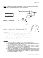
Figure 1:- PSK Circuit
http://mhakhan.tripod.com/lab.html
Page 19 of 26
OOK:- By shorting the 10 K resistor connected between pin # 2 & 6 of the PSK circuit shown in
Figure 1 above, it will now work as an OOK (ON-OFF Keying) circuit.
Vin
+
-
b2 = 0, vo = vin
b2 = 1, vo =3vin
10 Κ
4.7 K
33 K
Figure 2 :- ASK Circuit
Vo
b2
E
B C
Figure 3 :- Bottom View of NPN Transistor ( BC 147 )
Apparatus Used:1. Breadboard PDC-20 (having symmetrical dual DC power supply)
2. Components:Opamps (741) = 02 nos.
NPN Transistors (BC 147) = 02 nos
Resistors :- 100K = 1, 33K = 2, 10K = 3, 4.7K = 1
3. Function Generator Model ST-4062 = 1 (for carrier)
4. Function Generator (Pacific) Model FG-18 = 1 (for TTL Clock)
5. 20 MHz Dual Trace Oscilloscope = 1
Procedure:1. Construct the PSK circuit (as shown in Figure 1 above) on the Breadboard.
2. Keeping the DC power supply OFF, connect the +15 V terminal of the supply to pin # 7,
and –15 V terminal to pin # 4 of the opamp, 741, and the GND terminal to a common point
on the Breadboard, and turn ON the power supply now.
3. Obtain a sinusoidal signal from Function Generator Model ST-4062 and adjust its
amplitude around 0.5 V p-p and frequency around 8 KHz (by connecting it directly to
CRO), and connect it to the carrier input, Vin of the PSK circuit.
4. Obtain a TTL clock from the TTL output of the Function generator model FG-18, and
adjust its frequency around 1 to 2 KHz (by connecting it directly to CRO), and connect it
to modulating signal input b1 of the PSK circuit. [Note that a TTL clock is a binary pulsetrain (unipolar) of amplitude = +5-voltsp-p]
http://mhakhan.tripod.com/lab.html
Page 20 of 26
5. Ensure that all the GND terminals of both Function generators and the CRO are connected
together and are also connected to the common point made on the Breadboard.
6. Now, connect the TTL clock to one channel, and the output of the PSK circuit to the other
channel of the CRO, and adjust the triggering and the gain controls of the CRO properly to
obtain a clear wave shape of the PSK signal on the CRO screen. Note the shifting of the
phase at every transition point of the binary TTL clock.
7. Now, short circuit the 10K resistor connected between pin 2 & 6 of opamp in the PSK
Circuit, to get an OOK signal on the CRO screen.
8. Similarly, construct the ASK circuit (as shown in Figure 2 above) on the bread board,
connect biasing power supply and connect the previously adjusted sinusoidal carrier to the
Vin input of the ASK circuit, and a TTL clock to its b2 input and display b2 on one channel
and the output, Vo of the ASK, on another channel of the CRO, and note the shifting of the
amplitudes at the transition points of the binary TTL clock.
9. The APSK signal can be studied by connecting the output of the ASK to the carrier input
Vin , of the PSK circuit, (the sinusoidal carrier signal being connected to the carrier-input
of the ASK circuit), and connecting ‘1’ and ‘0’ to the binary inputs b1 and b2. For ‘1’,
connect +15 Volts DC supply and for ‘0’, connect Ground (0 Volt DC).
10. Measure and record the high and low values of the amplitudes of the APSK signal and the
phase difference of the APSK output with the carrier-input in a tabular form as shown
under observations and verify the truth-table for the APSK signal.
11. Draw all the above signals (PSK, OOK, ASK & APSK) clearly on a graph paper and mark
the shifting of phase and amplitude in the modulated signals corresponding to b1 and b2.
Continued to next page ---
Observations
Amplitude of the carrier = -------- Volts p-p
frequency of the carrier = -------- KHz
frequency of the TTL clock = -------- KHz
For ASK, high amplitude = ------- volts p-p, and low amplitude = ------- volts p-p
b1
0
0
1
1
b2
Amplitude
Phase-diff
0
1
0
1
NB:- For verifying truth table of the APSK, connect +15 V DC for logical ‘1’ and GND for ‘0’. Care
must be taken for proper grounding of the circuits and for proper triggering of the CRO.
***************
http://mhakhan.tripod.com/lab.html
Page 21 of 26
Experiment No. 7 - PCM
OBJECT:- (a) Study of TDM.
(b) Study of the Transmission and reception of two signals by PCM.
(c) Study of error- check codes: (i) Even and Odd parity codes
(ii) Hamming codes
EQUIPMENTS REQUIRED:1.
PCM Transmitter kit, Scientech model ST2103 - Tx
2.
PCM Receiver kit, Scientech model ST2104 - Rx
3.
20 MHz Dual Trace CRO / DSO
4.
Patch cords
PROCEDURE:(a) For TDM:1. Set up the following initial conditions on the PCM Transmitter kit, ST2103:a) Mode Switch in ‘FAST’ position
b) DC 1 & DC2 Controls in function generator block fully clockwise.
c) Set ~ 1 KHz and ~2 KHz control levels to give 10 Vpp.
d) Pseudo - random sync code generator ON/'OFF' switch in 'OFF' Position.
e) Error check code generator switch A & B in A=0 & B=0 position ('Off' Mode)
f) All switched faults to 'Off'.
2. First, connect only the ~1 KHz output to CH 0
3. Turn ON the power. Check that the PAM output of 1 KHz sine wave is available at TP15 of the
ST2103.
4. Connect channel 1 of the oscilloscope to TP10 & channel 2 of the oscilloscope to TP15, and
observe the timing & phase relation between the sampling signal TP10 & the sampled waveform at
TP15.
5. Turn 'Off' the power supply. Now connect also the 2 KHz supply to CH 1.
6. Connect channel 1 of the oscilloscope to TP12 & channel 2 of the oscilloscope to TP15.
7. Observe & explain the timing relation between the signals at TP10, 5, 6, 12 &15.
8. Draw the wave-shape of TDM signal on a graph paper and record all concerned parameters in your
observations.
(b) For PCM:1. Using the same setup of initial conditions as already done in step 1 above, make the following
connections:(a) Connect the Ground of the Tx-kit (2103) to the Ground of the Rx-kit (2104),
http://mhakhan.tripod.com/lab.html
Page 22 of 26
(b) Connect the Tx Clock (3) of Tx-kit (2103) to the Rx-Clock (46) on the Rx-kit (2104),
c) Connect the Tx Sync (4) of Tx-kit (2103) to the Rx-Sync (47) on the Rx-kit (2104),
d) Connect the PCM Output (44) on Tx-kit (2103) to the PCM Data input (1) on the Rx-kit.
e) Connect the message signals of ~1KHz to CH-0 (10) and ~2 KHz to CH-1 (12) on the Tx-kit
2. Now, observe the PCM Output at (44), on one channel of the oscilloscope.
3. Observe the effect of amplitude variation of the above message signals on the PCM output.
4. Draw the wave-shape of PCM signal on a graph paper.
Now, observe the recovered message signals at CH0 (33) & at CH1 (36) in the Rx-kit, on CRO, and
compare them with the transmitted message signals connected on the Tx-kit, note their parameters and
report the result of your comparisons.
*************
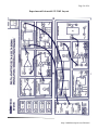
PCM Transmitter and Receiver Layout diagrams
Connections for TDM and PCM
***************
http://mhakhan.tripod.com/lab.html
Page 23 of 26
Experimemt No. 8 : Delta Modulation
Object:- a) Generate Delta modulated signal using the given Scientech kit model ST-2105.
b) Determine the conditions for slope-overloading.
c) Study the elimination of the slope-overloading by adjusting various parameters.
APPARATUS USED:1. Scientech Delta Modulation Trainer kit Model ST-2105
2. 20 MHz Dual Channel Oscilloscope
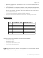
14
9
Delta
Modulator
m(t)
S(t)
= DM O/P in Encoded form
m(t) = Integrator's O/P in Staircase form
17
13
Clock
Input
DELTA MODULATION
Schematic Diagram for Delta modulation:The following sections of the given kit are to be used for this experiment on Delta Modulation:1. Function Generator section providing sinusoidal signals (to be used as modulating signals) of
adjustable amplitudes and of 250 Hz, 500 Hz, 1 KHz and 2 KHz frequencies.
2. CLOCK Generator section providing clocks of adjustable frequencies of 32 KHz, 64 KHz, 128
KHz and 256 KHz (to be used as a carrier of given sampling rates).
3. A COMPARATOR Circuit (in the Transmitter Part of the kit).
4. A BISTABLE Circuit (in the Transmitter Part of the kit) with “LEVEL CHANGER” control.
5. An INTEGRATOR Circuit (in the Transmitter Part of the kit) with adjustable gain control.
6. A Unipolar to Bipolar Converter section (in the Transmitter Part of the kit).
The above sections of the kit are to be inter-connected according to the following Schematic diagram:-
m(t)
Message Input
9
+
COMPARATOR
10
12
11
Q
D
14
S(t)
BISTABLE
Circuit
-
13
CLK Input (fs)
CLK
LEVEL CHANGER
m(t)
17
INTEGRATOR
16
15
Unipolar
to
Bipolar Converter
http://mhakhan.tripod.com/lab.html
Page 24 of 26
PROCEDURE:1. Adjust the Clock frequency (sampling rate) to 32 KHz ( by setting the switches A = 0, B = 0).and
connect it to socket number (13) in the “BISTABLE Circuit (in the Transmitter Part of the kit)”.
2. Adjust the “Step size”, by connecting 0-volt to the positive-input (9) of the COMPARATOR
Circuit and monitor on an Oscilloscope, the output of Integrator 1 (t.p.17) and the output of the
transmitter’s LEVEL CHANGER (t.p15).
3. Ensure that integrator 1 block’s switches are in following position:
(A) Gain control switch in left-hand position (towards switch A & B).
(B) Switches A & B in A=0 and B=0 positions, corresponding to the minimum gain.
4. Adjust the transmitter’s LEVEL CHANGER preset until the output of INTEGRATOR 1 (t.p. 17) is a
triangle wave centered around 0 Volts. The peak-to-peak amplitude of the triangle wave at the integrator’s
output should be 0.5V (approx), this amplitude is known as the integrator STEP SIZE Δ. The output
from the Transmitter’s BISTABLE Circuit (t.p. 14) will now be a stream of alternate ‘1’ and ‘0’, this is
also the output of the delta modulator itself. The Delta Modulator is now said to be ‘balanced’ for correct
operation.
5. Now remove the 0-volt from the positive-input (9) of the COMPARATOR Circuit and connect a
Sine-wave (as a message signal) of 500 Hz (obtained from the Function Generator section) to the
positive-input terminal (9) of the COMPARATOR Circuit.
6. Observe the “Integrator’s output” m(t) at (17) on one channel of the CRO.
7. Adjust the “TRANSMITTER LEVEL ADJ Preset” (provided in the BISTABLE Circuit) in order to
obtain a stable trace of “Integrator’s output” m(t) at (17).
8. Now observe the sinusoidal message signal of 500 Hz connected at (9) of the Comparator on the
other channel of the CRO, and after adjusting the CRO controls, observe that the “Integrator’s output”
m(t) at (17), is following the message signal m(t) on the CRO screen. This ensures the correct
operation of Delta modulation; and the “encoded Delta modulated signal S(t)” is now available at
the output of the BISTABLE Circuit at socket (14). View it on the CRO and observe that it is a stream
of ‘1s’ and ‘0s’.
9. Record all the parameters adjusted for this setting in your observations. This completes the first
part (a) of this experiment.
Now proceed for taking observations for slope-overloading as required for part (b) of the
experiment in the following way:1. Increase the frequency of the message signal m(t) by connecting a 1 KHz and then a 2 KHz sinewave to the Comparator’s input (one by one), and record the maximum frequency of the m(t) in your
observations, at which the “Integrator’s output” m(t) ceases to follow the message signal m(t) on the
http://mhakhan.tripod.com/lab.html
Page 25 of 26
CRO. The condition in which the “Integrator’s output” is no longer following the message is called
“slope over-loading”. This gives the first condition of slope over-loading.
2. Now restore the message frequency and start increasing the message amplitude, until you again observe
the slope-overloading. Record the maximum message amplitude in your observations at which the slopeoverloading is occurring, which is the second condition of slope-overloading.
Next, for part (c) of the experiment, proceed as follows:1. First observe the slope-overloading at the maximum message frequency (as already done in part b),
then, increase the step-size Δ, by increasing the integrator’s gain by setting the integrator switches A & B
accordingly, and observe that, at what setting of integrator’s gain switches, the slope-overloading is
eliminated and the “Integrator’s output” m(t) again starts to follow the message signal m(t). Record the
value of the step-size Δ (in volt) in your observations, at which the slope-overloading is eliminated.
2. Similarly, get the slope-overloading at the maximum message amplitude (as already done in part b) and
eliminate it by again increasing the step-size Δ (as done in the above step) and record it in your
observations.
3. Also, try to eliminate the slope-overloading by increasing the sampling frequency.
OBSERVATIONS:(a) For the proper occurrence of Delta Modulation (no slope-overloading) :-
Amplitude of the sinusoidal (message) signal, Am = …………. Volts p-p
Frequency of the sinusoidal (message) signal, fm = …………. KHz
Sampling frequency, fs = ………….. KHz,
Step-size. Δ = …………….. volts, p-p
(b) Conditions for slope-overloading :Maximum frequency of the message, causing slope-overloading = …………… KHz
Maximum amplitude of the message, causing slope-overloading = …………… Volts p-p
(c) For elimination of slope-overloading:(i) Step-size (for eliminating slope-overloading at maximum message freq. of …. KHz) = …. Volt
(ii) Step-size (for eliminating slope-overloading at max. message amplitude of …. volts p-p) = …. Volt
(iii) Sampling frequency (for eliminating slope-overloading at max. message freq. of . KHz) = … KHz
References:- 1. For understanding the operations of the various sections of the kit, refer to the
“Manual of the Scientech Delta modulation Trainer kit, model ST-2105”.
2. For theory of the Delta Modulation, refer to the Textbooks prescribed on Digital Communication.
************
http://mhakhan.tripod.com/lab.html
Page 26 of 26
Experimental kit model ST-2105 Layout
**********
http://mhakhan.tripod.com/lab.html