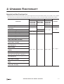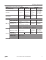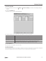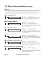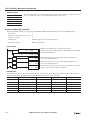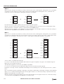
1
FC9Y-B927-ADD FC5A SERIES Micro Programmable Logic Controller User’s Manual Supplement System Program Version 101 to 210 SAFETY PRECAUTIONS • Read this user’s manual to make sure of correct operation before starting installation, wiring, operation, maintenance, and inspection of the MicroSmart. • All MicroSmart modules are manufactured under IDEC’s rigorous quality control system, but users must add a backup or failsafe provision to the control system using the MicroSmart in applications where heavy damage or personal injury may be caused in case the MicroSmart should fail. • In this user’s manual, safety precautions are categorized in order of importance to Warning and Caution: Warning Warning notices are used to emphasize that improper operation may cause severe personal injury or death. • Turn off the power to the MicroSmart before starting installation, removal, wiring, maintenance, and inspection of the MicroSmart. Failure to turn power off may cause electrical shocks or fire hazard. • Special expertise is required to install, wire, program, and operate the MicroSmart. People without such expertise must not use the MicroSmart. • Emergency stop and interlocking circuits must be configured outside the MicroSmart. If such a circuit is configured inside the MicroSmart, failure of the MicroSmart may cause disorder of the control system, damage, or accidents. • Install the MicroSmart according to the instructions described in this user’s manual. Improper installation will result in falling, failure, or malfunction of the MicroSmart. Caution Caution notices are used where inattention might cause personal injury or damage to equipment. • The MicroSmart is designed for installation in a cabinet. Do not install the MicroSmart outside a cabinet. • Install the MicroSmart in environments described in this user’s manual. If the MicroSmart is used in places where the MicroSmart is subjected to high-temperature, high-humidity, condensation, corrosive gases, excessive vibrations, and excessive shocks, then electrical shocks, fire hazard, or malfunction will result. • The environment for using the MicroSmart is “Pollution degree 2.” Use the MicroSmart in environments of pollution degree 2 (according to IEC 60664-1). • Prevent the MicroSmart from falling while moving or transporting the MicroSmart, otherwise damage or malfunction of the MicroSmart will result. • Prevent metal fragments and pieces of wire from dropping inside the MicroSmart housing. Put a cover on the MicroSmart modules during installation and wiring. Ingress of such fragments and chips may cause fire hazard, damage, or malfunction. • Use a power supply of the rated value. Use of a wrong power supply may cause fire hazard. • Use an IEC 60127-approved fuse on the power line outside the MicroSmart. This is required when equipment containing the MicroSmart is destined for Europe. • Use an IEC 60127-approved fuse on the output circuit. This is required when equipment containing the MicroSmart is destined for Europe. • Use an EU-approved circuit breaker. This is required when equipment containing the MicroSmart is destined for Europe. • Make sure of safety before starting and stopping the MicroSmart or when operating the MicroSmart to force outputs on or off. Incorrect operation on the MicroSmart may cause machine damage or accidents. • If relays or transistors in the MicroSmart output modules should fail, outputs may remain on or off. For output signals which may cause heavy accidents, provide a monitor circuit outside the MicroSmart. • Do not connect the ground wire directly to the MicroSmart. Connect a protective ground to the cabinet containing the MicroSmart using an M4 or larger screw. This is required when equipment containing the MicroSmart is destined for Europe. • Do not disassemble, repair, or modify the MicroSmart modules. • Dispose of the battery in the MicroSmart modules when the battery is dead in accordance with pertaining regulations. When storing or disposing of the battery, use a proper container prepared for this purpose. This is required when equipment containing the MicroSmart is destined for Europe. • When disposing of the MicroSmart, do so as an industrial waste. FC5A MICROSMART USER’S MANUAL SUPPLEMENT PREFACE-1 About This Manual This user’s manual supplement primarily describes in detail the upgraded and new functions added since FC5A MicroSmart system program version 101 up to 210. CHAPTER 1: UPGRADED FUNCTIONALITY The list of upgraded and new functions. CHAPTER 2: MODULE SPECIFICATIONS Updated specifications of analog I/O modules. CHAPTER 5: SPECIAL FUNCTIONS Upgraded functions including HMI module, expansion RS232C communication module, Modbus, 32-bit data storage setting, forced I/O, Run LED flashing mode, memory cartridge upload, user program protection upgrade, and key matrix input. CHAPTER 7: BASIC INSTRUCTIONS Programming and sample programs of new basic instructions TMLO, TIMO, TMHO, TMSO, CNTD, CDPD, and CUDD. CHAPTERS 8 TO 18 AND CHAPTERS 33 TO 34: ADVANCED INSTRUCTIONS Programming and sample programs of upgraded advanced instructions MOV, IMOV, CMP, ADD, SUB, MUL, DIV, ROOT, BTOA, ATOB, and RXD instructions. Also included are new advanced instructions NSET, NRS, XCHG, TCCST, LC, INC, DEC, SUM, RNDM, DTDV, DTCB, SWAP, DJNZ, FIFOF, FIEX, FOEX, NDSRC, TADD, TSUB, HTOS, STOH, and HOUR. CHAPTER 32: TROUBLESHOOTING Additional user program execution error codes related to the new advanced instructions. APPENDIX Additional information about execution times for instructions, instruction steps and applicability in interrupt programs, and procedure to upgrade FC5A MicroSmart system program. Also included are corrections in the FC5A MicroSmart User’s Manual FC9Y-B927-0. INDEX Alphabetical listing of key words. IMPORTANT INFORMATION Under no circumstances shall IDEC Corporation be held liable or responsible for indirect or consequential damages resulting from the use of or the application of IDEC PLC components, individually or in combination with other equipment. All persons using these components must be willing to accept responsibility for choosing the correct component to suit their application and for choosing an application appropriate for the component, individually or in combination with other equipment. All diagrams and examples in this manual are for illustrative purposes only. In no way does including these diagrams and examples in this manual constitute a guarantee as to their suitability for any specific application. To test and approve all programs, prior to installation, is the responsibility of the end user. PREFACE-2 FC5A MICROSMART USER’S MANUAL SUPPLEMENT TABLE OF CONTENTS CHAPTER 1: UPGRADED FUNCTIONALITY Upgraded and New Functions List . . . . . . . . . . . . . . . . . . . . . . . . . . . . . . . . . . . . . 1-1 CHAPTER 2: MODULE SPECIFICATIONS Analog I/O Module Specifications . . . . . . . . . . . . . . . . . . . . . . . . . . . . . . . . . . . . . 2-1 CHAPTER 5: SPECIAL FUNCTIONS HMI Module . . . . . . . . . . . . . . . . . . . . . . . . . . . . . . . . . . . . . . . . . . . . . . . . . . . . 5-1 Expansion RS232C Communication Module . . . . . . . . . . . . . . . . . . . . . . . . . . . . . 5-2 Modbus Communication . . . . . . . . . . . . . . . . . . . . . . . . . . . . . . . . . . . . . . . . . . . 5-3 32-bit Data Storage Setting . . . . . . . . . . . . . . . . . . . . . . . . . . . . . . . . . . . . . . . . . 5-4 Forced I/O . . . . . . . . . . . . . . . . . . . . . . . . . . . . . . . . . . . . . . . . . . . . . . . . . . . . . 5-7 RUN LED Flashing Mode . . . . . . . . . . . . . . . . . . . . . . . . . . . . . . . . . . . . . . . . . . . 5-9 Memory Cartridge Upload . . . . . . . . . . . . . . . . . . . . . . . . . . . . . . . . . . . . . . . . . . 5-10 User Program Protection Upgrade . . . . . . . . . . . . . . . . . . . . . . . . . . . . . . . . . . . . 5-11 Key Matrix Input . . . . . . . . . . . . . . . . . . . . . . . . . . . . . . . . . . . . . . . . . . . . . . . . 5-12 CHAPTER 7: BASIC INSTRUCTIONS Basic Instruction List . . . . . . . . . . . . . . . . . . . . . . . . . . . . . . . . . . . . . . . . . . . . . . 7-1 TMLO, TIMO, TMHO, and TMSO (Off-Delay Timer) . . . . . . . . . . . . . . . . . . . . . . . . . . 7-2 CNTD, CDPD, and CUDD (Double-Word Counter) . . . . . . . . . . . . . . . . . . . . . . . . . . 7-3 CHAPTER 8: ADVANCED INSTRUCTIONS Advanced Instruction List . . . . . . . . . . . . . . . . . . . . . . . . . . . . . . . . . . . . . . . . . . . 8-1 Advanced Instruction Applicable CPU Modules . . . . . . . . . . . . . . . . . . . . . . . . . . . . 8-3 CHAPTER 9: MOVE INSTRUCTIONS MOV (Move) . . . . . . . . . . . . . . . . . . . . . . . . . . . . . . . . . . . . . . . . . . . . . . . . . . . . IMOV (Indirect Move) . . . . . . . . . . . . . . . . . . . . . . . . . . . . . . . . . . . . . . . . . . . . . . NSET (N Data Set) . . . . . . . . . . . . . . . . . . . . . . . . . . . . . . . . . . . . . . . . . . . . . . . . NRS (N Data Repeat Set) . . . . . . . . . . . . . . . . . . . . . . . . . . . . . . . . . . . . . . . . . . . XCHG (Exchange) . . . . . . . . . . . . . . . . . . . . . . . . . . . . . . . . . . . . . . . . . . . . . . . . . TCCST (Timer/Counter Current Value Store) . . . . . . . . . . . . . . . . . . . . . . . . . . . . . CHAPTER 10: 9-1 9-2 9-3 9-4 9-5 9-6 DATA COMPARISON INSTRUCTIONS CMP= (Compare Equal To) . . . . . . . . . . . . . . . . . . . . . . . . . . . . . . . . . . . . . . . . . CMP<> (Compare Unequal To) . . . . . . . . . . . . . . . . . . . . . . . . . . . . . . . . . . . . . . CMP< (Compare Less Than) . . . . . . . . . . . . . . . . . . . . . . . . . . . . . . . . . . . . . . . . CMP> (Compare Greater Than) . . . . . . . . . . . . . . . . . . . . . . . . . . . . . . . . . . . . . . CMP<= (Compare Less Than or Equal To) . . . . . . . . . . . . . . . . . . . . . . . . . . . . . . CMP>= (Compare Greater Than or Equal To) . . . . . . . . . . . . . . . . . . . . . . . . . . . . LC= (Load Compare Equal To) . . . . . . . . . . . . . . . . . . . . . . . . . . . . . . . . . . . . . . LC<> (Load Compare Unequal To) . . . . . . . . . . . . . . . . . . . . . . . . . . . . . . . . . . . LC< (Load Compare Less Than) . . . . . . . . . . . . . . . . . . . . . . . . . . . . . . . . . . . . . LC> (Load Compare Greater Than) . . . . . . . . . . . . . . . . . . . . . . . . . . . . . . . . . . . LC<= (Load Compare Less Than or Equal To) . . . . . . . . . . . . . . . . . . . . . . . . . . . LC>= (Load Compare Greater Than or Equal To) . . . . . . . . . . . . . . . . . . . . . . . . . FC5A MICROSMART USER’S MANUAL SUPPLEMENT 10-1 10-1 10-1 10-1 10-1 10-1 10-3 10-3 10-3 10-3 10-3 10-3 i TABLE OF CONTENTS CHAPTER 11: CHAPTER 14: CHAPTER 17: BINARY ARITHMETIC INSTRUCTIONS INC (Increment) . . . . . . . . . . . . . . . . . . . . . . . . . . . . . . . . . . . . . . . . . . . . . . . . . DEC (Decrement) . . . . . . . . . . . . . . . . . . . . . . . . . . . . . . . . . . . . . . . . . . . . . . . . SUM (Sum) . . . . . . . . . . . . . . . . . . . . . . . . . . . . . . . . . . . . . . . . . . . . . . . . . . . . RNDM (Random) . . . . . . . . . . . . . . . . . . . . . . . . . . . . . . . . . . . . . . . . . . . . . . . . 11-1 11-1 11-3 11-6 DATA CONVERSION INSTRUCTIONS BTOA (BCD to ASCII) . . . . . . . . . . . . . . . . . . . . . . . . . . . . . . . . . . . . . . . . . . . . . ATOB (ASCII to BCD) . . . . . . . . . . . . . . . . . . . . . . . . . . . . . . . . . . . . . . . . . . . . . DTDV (Data Divide) . . . . . . . . . . . . . . . . . . . . . . . . . . . . . . . . . . . . . . . . . . . . . . DTCB (Data Combine) . . . . . . . . . . . . . . . . . . . . . . . . . . . . . . . . . . . . . . . . . . . . SWAP (Data Swap) . . . . . . . . . . . . . . . . . . . . . . . . . . . . . . . . . . . . . . . . . . . . . . . 14-1 14-3 14-5 14-6 14-7 USER COMMUNICATION INSTRUCTIONS Multi-byte Start Delimiter . . . . . . . . . . . . . . . . . . . . . . . . . . . . . . . . . . . . . . . . . . Constant . . . . . . . . . . . . . . . . . . . . . . . . . . . . . . . . . . . . . . . . . . . . . . . . . . . . . . Variable Option for Data Register . . . . . . . . . . . . . . . . . . . . . . . . . . . . . . . . . . . . User Communication Error . . . . . . . . . . . . . . . . . . . . . . . . . . . . . . . . . . . . . . . . . 17-1 17-4 17-5 17-6 CHAPTER 18: PROGRAM BRANCHING INSTRUCTIONS DJNZ (Decrement Jump Non-zero) . . . . . . . . . . . . . . . . . . . . . . . . . . . . . . . . . . . . 18-1 CHAPTER 32: TROUBLESHOOTING User Program Execution Error . . . . . . . . . . . . . . . . . . . . . . . . . . . . . . . . . . . . . . . 32-1 CHAPTER 33: FILE DATA PROCESSING INSTRUCTIONS FIFOF (FIFO Format) . . . . . . . . . . . . . . . . . . . . . . . . . . . . . . . . . . . . . . . . . . . . . . FIEX (First-In Execute) . . . . . . . . . . . . . . . . . . . . . . . . . . . . . . . . . . . . . . . . . . . . . FOEX (First-Out Execute) . . . . . . . . . . . . . . . . . . . . . . . . . . . . . . . . . . . . . . . . . . . NDSRC (N Data Search) . . . . . . . . . . . . . . . . . . . . . . . . . . . . . . . . . . . . . . . . . . . CHAPTER 34: 33-1 33-3 33-3 33-5 CLOCK INSTRUCTIONS TADD (Time Addition) . . . . . . . . . . . . . . . . . . . . . . . . . . . . . . . . . . . . . . . . . . . . . 34-1 TSUB (Time Subtraction) . . . . . . . . . . . . . . . . . . . . . . . . . . . . . . . . . . . . . . . . . . . 34-5 HTOS (HMS to Sec) . . . . . . . . . . . . . . . . . . . . . . . . . . . . . . . . . . . . . . . . . . . . . . 34-9 STOH (Sec to HMS) . . . . . . . . . . . . . . . . . . . . . . . . . . . . . . . . . . . . . . . . . . . . . 34-10 HOUR (Hour Meter) . . . . . . . . . . . . . . . . . . . . . . . . . . . . . . . . . . . . . . . . . . . . . 34-11 APPENDIX Execution Times for Instructions . . . . . . . . . . . . . . . . . . . . . . . . . . . . . . . . . . . . . . Instruction Steps and Applicability in Interrupt Programs . . . . . . . . . . . . . . . . . . . . . Procedure to Upgrade FC5A MicroSmart System Program . . . . . . . . . . . . . . . . . . . . Corrections in the FC5A MicroSmart User’s Manual FC9Y-B927-0 . . . . . . . . . . . . . . INDEX ii FC5A MICROSMART USER’S MANUAL SUPPLEMENT A-1 A-2 A-3 A-5 1: UPGRADED FUNCTIONALITY Upgraded and New Functions List Upgraded and new functions listed below have been implemented in the FC5A MicroSmart CPU modules. The availability of these functions depends on the model and the system program version of the FC5A MicroSmart CPU modules: All-In-One Type FC5A-C10R2 FC5A-C10R2C FC5A-C16R2 FC5A-C16R2C CPU Module HMI Module Upgrade (Note 1) Slim Type FC5A-C24R2 FC5A-C24R2C 110 or higher Expansion RS232C Communication Module Compatibility 101 or higher — — 32-bit Data Storage Setting WindLDR — 110 or higher Modbus Master Upgrade (Note 2) Modbus Slave Upgrade (Note 2) FC5A-D16RK1 FC5A-D16RS1 FC5A-D32K3 FC5A-D32S3 110 or higher 110 or higher 200 or higher 200 or higher 110 or higher 5.1 or higher Forced I/O RUN LED Flashing Mode Memory Cartridge Upload Function (Note 3) Off-Delay Timer Instructions (TMLO, TIMO, TMHO, and TMSO) Double-Word Counter Instructions (CNTD, CDPD, and CUDD) MOV and IMOV Instructions Upgrade (New data type F) N Data Set and N Data Repeat Set Instructions (NSET and NRS) Timer/Counter Current Value Store Instruction (TCCST) 200 or higher 5.2 or higher CMP Instructions Upgrade Load Comparison Instructions (LC=, LC<>, LC<, LC>, LC<=, and LC>=) BTOA and ATOB Instructions Upgrade (New data type D) Data Divide, Combine, and Swap Instructions (DTDV, DTCB, and SWAP) User Communication Instructions Upgrade (RXD) File Processing Instructions (FIFOF, FIEX, and FOEX) FC5A MICROSMART USER’S MANUAL SUPPLEMENT 1-1 1: UPGRADED FUNCTIONALITY All-In-One Type FC5A-C10R2 FC5A-C10R2C FC5A-C16R2 FC5A-C16R2C CPU Module Key Matrix Input Slim Type FC5A-C24R2 FC5A-C24R2C FC5A-D16RK1 FC5A-D16RS1 FC5A-D32K3 FC5A-D32S3 210 or higher 210 or higher WindLDR — User Program Protection Upgrade Exchange Instruction (XCHG) Increment Instruction (INC) Decrement Instruction (DEC) Sum Instruction (SUM) 210 or higher 5.3 or higher Random Instruction (RNDM) Decrement Jump Non-zero (DJNZ) N Data Search Instruction (NDSRC) Clock Instructions (TADD, TSUB, HTOS, STOH, and HOUR) To confirm the system program version of the MicroSmart CPU module, use WindLDR on a computer connected with the CPU module. Bring WindLDR into the online mode. The system program version is indicated on the PLC Status dialog box. Note 1: The optional HMI module (FC4A-PH1) is needed to use this function. Note 2: Modbus Master or Slave function can be used on the Port 2 of the MicroSmart CPU modules only. Note 3: Memory cartridge (FC4A-PM32 or FC4A--PM64) is required to use this function. 1-2 FC5A MICROSMART USER’S MANUAL SUPPLEMENT 2: MODULE SPECIFICATIONS Introduction This chapter describes updated analog I/O module specifications. Analog I/O Module Specifications General Specifications (END Refresh Type) Type No. FC4A-L03A1 FC4A-L03AP1 FC4A-J2A1 FC4A-K1A1 Rated Power Voltage 24V DC Allowable Voltage Range 20.4 to 28.8V DC Terminal Arrangement See Analog I/O Module Terminal Arrangement on pages 2-52 to 2-55 of the FC5A MicroSmart Pentra User’s Manual (FC9Y-B927). Connector on Mother Board MC1.5/11-G-3.81BK (Phoenix Contact) Connector Insertion/Removal Durability 100 times minimum Internal Current Draw 50 mA (5V DC) 0 mA (24V DC) 50 mA (5V DC) 0 mA (24V DC) 50 mA (5V DC) 0 mA (24V DC) 50 mA (5V DC) 0 mA (24V DC) External Current Draw (Note) 45 mA (24V DC) 40 mA (24V DC) 35 mA (24V DC) 40 mA (24V DC) Weight 85g Note: The external current draw is the value when all analog inputs are used and the analog output value is at 100%. General Specifications (Ladder Refresh Type) Type No. FC4A-J4CN1 FC4A-J8C1 FC4A-J8AT1 FC4A-K2C1 Rated Power Voltage 24V DC Allowable Voltage Range 18.0 to 30.0V DC Terminal Arrangement See Analog I/O Module Terminal Arrangement on pages 2-52 to 2-55 of the FC5A MicroSmart Pentra User’s Manual (FC9Y-B927). Connector on Mother Board MC1.5/10-G-3.81BK (Phoenix Contact) Connector Insertion/Removal Durability 100 times minimum Internal Current Draw 50 mA (5V DC) 0 mA (24V DC) 40 mA (5V DC) 0 mA (24V DC) 45 mA (5V DC) 0 mA (24V DC) 60 mA (5V DC) 0 mA (24V DC) External Current Draw (Note) 55 mA (24V DC) 50 mA (24V DC) 55 mA (24V DC) 85 mA (24V DC) Weight 140g 140g 125g 110g Note: The external current draw is the value when all analog inputs are used and the analog output value is at 100%. FC5A MICROSMART USER’S MANUAL SUPPLEMENT 2-1 2: MODULE SPECIFICATIONS Analog Input Specifications (END Refresh Type) Type No. FC4A-L03A1 / FC4A-J2A1 Input Range 0 to 10V DC 4 to 20 mA DC Input Impedance Allowable Conductor Resistance (per wire) Input Detection Current Sample Duration Time Sample Repetition Time Total Input System Transfer Time (Note 1) AD Conversion Type of Input 1 MΩ minimum 10Ω FC4A-L03AP1 Resistance Thermocouple Thermometer Type K (0 to 1300°C) Pt 100 Type J 3-wire type (0 to 1200°C) (–100 to 500°C) Type T (0 to 400°C) 1 MΩ minimum 1 MΩ minimum — — — 200Ω maximum — — 20 ms maximum 20 ms maximum — 20 ms maximum 20 ms maximum 1.0 mA maximum 105 ms + 1 scan time 200 ms + 1 scan time Analog Input Signal Type Voltage Input Operating Mode Conversion Method Input Error Data Noise Resistance Single-ended input Self-scan ∑∆ type ADC Current Input Differential input ±0.2% of full scale K: 0.325°C J: 0.300°C T: 0.100°C 0.15°C Maximum Error at 25°C ±0.2% of full scale Temperature Coefficient Repeatability after Stabilization Time Non-lineality Maximum Error Digital Resolution ±0.006% of full scale/°C Input Value of LSB 2.5 mV Data Type in Application Program Monotonicity Input Data Out of Range Maximum Temporary Deviation during Electrical Noise Tests Input Filter Recommended Cable for Noise Immunity Crosstalk Default: 0 to 4095 Optional: –32768 to 32767 (selectable each channel) (Note 2) Yes Detectable (Note 3) ±3% maximum (when a 500V clamp voltage is applied to the power Not assured supply and I/O lines) No Isolation Effect of Improper Input Connection Maximum Permanent Allowed Overload (No Damage) Selection of Analog Input Signal Type Calibration or Verification to Maintain Rated Accuracy ±0.5% of full scale ±0.2% of full scale ±1% of full scale 4096 increments (12 bits) 4 µA Twisted pair shielded cable — 2 LSB maximum Isolated between input and power circuit Photocoupler-isolated between input and internal circuit No damage 13V DC 40 mA DC Using software programming Impossible For Note 1 through Note 3, see page 2-6. 2-2 ±0.2% of full scale + reference junction compensation accuracy (±4°C maximum) FC5A MICROSMART USER’S MANUAL SUPPLEMENT — 2: MODULE SPECIFICATIONS Analog Input Specifications (Ladder Refresh Type) Type No. FC4A-J4CN1 / FC4A-J8C1 Analog Input Signal Type Voltage Input Input Range 0 to 10V DC Current Input 4 to 20 mA DC FC4A-J4CN1: 7Ω FC4A-J8C1: 100Ω — FC4A-J4CN1 Resistance Thermocouple Thermometer Type K: Pt100, Pt1000: 0 to 1300°C –100 to 500°C Type J: 0 to 1200°C Ni100, Ni1000: Type T: –60 to 180°C 0 to 400°C 1 MΩ Input Impedance 1 MΩ Input Detection Current Sample Duration Time — — 2 ms maximum FC4A-J4CN1: 10 ms maximum 30 ms maximum FC4A-J8C1: 2 ms maximum FC4A-J4CN1: 85 ms 50 ms × channels + 1 scan time × channels FC4A-J8C1: + 1 scan time 8 ms × channels + 1 scan time Single-ended input Self-scan FC4A-J4CN1: ∑∆ type ADC FC4A-J8C1: Successive approximation register method Sample Repetition Time AD Conversion Total Input System Transfer Time (Note 1) Type of Input Operating Mode Conversion Method Maximum Error at 25°C Input Error Cold Junction Compensation Error Temperature Coefficient Repeatability after Stabilization Time Non-lineality Maximum Error ±0.2% of full scale — — — 0.1 mA 10 ms maximum 50 ms × channels + 1 scan time ±0.2% of full scale + cold junction compensation error (±3°C maximum) Pt100, Ni100: ±0.4% of full scale Pt1000, Ni1000: ±0.2% of full scale ±3.0°C maximum — ±0.005% of full scale/°C ±0.5% of full scale ±0.04% of full scale ±1% of full scale FC5A MICROSMART USER’S MANUAL SUPPLEMENT 2-3 2: MODULE SPECIFICATIONS Type No. FC4A-J4CN1 / FC4A-J8C1 Analog Input Signal Type Voltage Input Current Input FC4A-J4CN1 Resistance Thermocouple Thermometer Pt100: Approx. 6400 increments K: Approx. 24000 increments (15 bits) J: Approx. Digital Resolution 50000 increments (16 bits) 33000 increments (15 bits) T: Approx. 10000 increments (14 bits) Data Data Type in Application Program Noise Resistance Monotonicity Input Data Out of Range Maximum Temporary Deviation during Electrical Noise Tests Input Filter Recommended Cable for Noise Immunity Crosstalk Isolation Effect of Improper Input Connection Maximum Permanent Allowed Overload (No Damage) Selection of Analog Input Signal Type Calibration or Verification to Maintain Rated Accuracy Twisted pair cable — 2 LSB maximum Isolated between input and power circuit Photocoupler-isolated between input and internal circuit No damage 11V DC 22 mA DC Using software programming Impossible For Note 1 through Note 3, see page 2-6. 2-4 64000 increments (16 bits) Ni100: Approx. 4700 increments (13 bits) Ni1000: Approx. 47000 increments (16 bits) Pt100: 0.086°C Pt1000: 0.0086°C 0.2 mV 0.32 µA Ni100: 0.037°C Ni1000: 0.0037°C Pt100, Ni100: 0 to 6000 Default: Default: 0 to 50000 0 to 50000 Pt1000, Ni1000: 0 to 60000 Optional: –32768 to 32767 (selectable for each channel) (Note 2) — Temperature: Celsius, Fahrenheit Yes Detectable (Note 3) ±3% maximum (when a 500V clamp voltage is applied to the power sup- Not assured ply and I/O lines) Software K: 0.058°C J: 0.038°C T: 0.042°C Input Value of LSB (13 bits) Pt1000: Approx. FC5A MICROSMART USER’S MANUAL SUPPLEMENT — 2: MODULE SPECIFICATIONS Analog Input Specifications (Ladder Refresh Type) Type No. Analog Input Signal Type Input Range Applicable Thermistor Input Detection Current Sample Duration Time Sample Repetition Time Total Input System AD Transfer Time (Note 1) Conversion Type of Input Operating Mode Conversion Method Maximum Error at 25°C Temperature Coefficient Repeatability after Input Error Stabilization Time Non-lineality Maximum Error Digital Resolution Input Value of LSB Data Noise Resistance Data Type in Application Program Monotonicity Input Data Out of Range Maximum Temporary Deviation during Electrical Noise Tests Input Filter Recommended Cable for Noise Immunity Crosstalk Isolation Effect of Improper Input Connection Selection of Analog Input Signal Type Calibration or Verification to Maintain Rated Accuracy FC4A-J8AT1 NTC –50 to 150°C 100 kΩ maximum 0.1 mA 2 ms maximum 2 ms maximum PTC 10 ms × channels + 1 scan time (Note 1) Single-ended input Self-scan Successive approximation register method ±0.2% of full scale ±0.005% of full scale/°C ±0.5% of full scale No ±1% of full scale Approx. 4000 increments (12 bits) 0.05°C Default: 0 to 4000 Optional: –32768 to 32767 (selectable for each channel) (Note 2) Temperature: Celsius, Fahrenheit (NTC only) Resistance: 0 to 10000 Yes Detectable (Note 3) ±3% maximum (when a 500V clamp voltage is applied to the power supply and I/O lines) Software — 2 LSB maximum Isolated between input and power circuit Photocoupler-isolated between input and internal circuit No damage Using software programming Impossible For Note 1 through Note 3, see page 2-6. FC5A MICROSMART USER’S MANUAL SUPPLEMENT 2-5 2: MODULE SPECIFICATIONS Analog Output Specifications Category Type No. END Refresh Type FC4A-L03AP1 Voltage Output Range Current Load Impedance Load Applicable Load Type Settling Time DA Total Output System Conversion Transfer Time Maximum Error at 25°C Temperature Coefficient Repeatability after Stabilization Time Output Error Output Voltage Drop Non-lineality Output Ripple Overshoot Total Error Digital Resolution Output Value of LSB FC4A-L03A1 FC4A-K1A1 0 to 10V DC 4 to 20 mA DC 2 kΩ minimum (voltage), 300Ω maximum (current) Resistive load 50 ms 130 ms 50 ms Settling time + 1 scan time Ladder Refresh FC4A-K2C1 –10 to +10V DC 1 ms/ch 1 ms × channels + 1 scan time ±0.2% of full scale ±0.015% of full scale/°C ±0.005% of full scale/°C ±0.5% of full scale ±1% of full scale ±0.2% of full scale 1 LSB maximum 0% ±1% of full scale ±0.1% of full scale 50000 increments (16 bits) 2.5 mV 0.4 mV 4 µA 0.32 µA –25000 to 25000 (voltage) Default: 0 to 4095 (voltage, current) 0 to 50000 (current) Optional: –32768 to 32767 (selectable for each channel) (Note 2) Yes Not detectable 4096 increments (12 bits) Voltage Current Data Data Type in Application Program Monotonicity Current Loop Open Maximum Temporary Deviation during Electrical Noise Tests Noise Resistance Recommended Cable for Noise Immunity Crosstalk Isolation Effect of Improper Output Connection Selection of Analog Output Signal Type Calibration or Verification to Maintain Rated Accuracy ±3% maximum (when a 500V clamp voltage is applied to the power supply and I/O lines) Twisted pair shielded cable Twisted pair cable No crosstalk because of 1 channel output 2 LSB maximum Isolated between output and power circuit Photocoupler-isolated between output and internal circuit No damage Using software programming Impossible Note 1: Total input system transfer time = Sample repetition time + Internal processing time When using the FC4A-J4CN1, FC4A-J8C1, or FC4A-J8AT1, the total input system transfer time increases in proportion to the number of channels used. Note 2: The data processed in the analog I/O module can be linear-converted to a value between –32768 and 32767. The optional range designation, and analog I/O data minimum and maximum values can be selected using data registers allocated to analog I/O modules. See page 26-12 of the FC5A MicroSmart Pentra User’s Manual (FC9Y-B927). Note 3: When an error is detected, a corresponding error code is stored to a data register allocated to analog I/O operating status. See page 26-6 of the FC5A MicroSmart Pentra User’s Manual (FC9Y-B927). 2-6 FC5A MICROSMART USER’S MANUAL SUPPLEMENT 5: SPECIAL FUNCTIONS HMI Module Two HMI module functions have been added to the MicroSmart CPU modules: clearing changed timer/counter preset values and displaying user program execution error code. These two functions can be used on the all-in-one type CPU modules system program version 110 or higher and the slim type CPU modules system program version 101 or higher. Clearing Changed Timer/Counter Preset Values This section describes the procedure for displaying and clearing the changed timer/counter preset values. 1. Select the Timer/Counter Changed Preset Value Confirm/Cancel menu. OK ▲ Display the TIM/CNT change status to confirm. Display the TIM/CNT change status to clear. TIM/CNT change status 0: Unchanged 1: Changed 2. Clear the changed timer/counter preset values in the RAM. OK ESC Clear the changed TIM/CNT preset values. Return to the Timer/Counter Changed Preset Value Confirm/Cancel menu. Note: To abort canceling the changed timer/counter preset values, press the ESC or ▲ button instead of the OK button; the Timer/Counter Changed Preset Value Confirm/Clear menu is restored. Displaying User Program Execution Error Code This section describes the procedure for displaying user program execution error code. 1. Select the Error menu. OK Go to control screen. 2. General error codes are displayed. ▲ Go to next screen to display the user program execution error code 3. User program execution error code is displayed. ▼ Return to the previous screen Notes: • Press the ESC button on any control screens to restore the Error menu. • User program execution error code cannot be cleared on HMI module. • For details about the definition of general error codes and user program execution error code, see pages 32-3 and 32-6 of the FC5A MicroSmart Pentra User’s Manual (FC9Y-B927). FC5A MICROSMART USER’S MANUAL SUPPLEMENT 5-1 5: SPECIAL FUNCTIONS Expansion RS232C Communication Module Expansion RS232C Communication Module is supported with system program version 110 or higher. The module is an expansion module of FC5A MicroSmart Pentra CPU modules and can be mounted on the right side of the CPU modules. For details on the module, see the FC5A Series Expansion RS232C Communication Module User’s Manual (FC9Y-B969). CPU Module Type 5-2 Maximum Number of Expansion RS232C Communication Modules FC5A-C10R2, FC5A-C10R2C FC5A-C16R2, FC5A-C16R2C — FC5A-C24R2, FC5A-C24R2C 3 FC5A-D16RK1, FC5A-D16RS1 FC5A-D32K3, FC5A-32S3 5 FC5A MICROSMART USER’S MANUAL SUPPLEMENT 5: SPECIAL FUNCTIONS Modbus Communication Modbus Master Communication Upgrades Modbus master communication has been upgraded with two functions. These two functions can be used on MicroSmart slim type CPU modules only. Number of Requests The number of requests entered in the Request Table dialog box has increased from 255 to 2040. Request Execution Relay Data register can be used as the Request Execution Relay of Modbus master communication. When the first data register number is designated as the Request Execution Relay, data register bits as many as the number of requests are allocated from the least significant bit of the first data register. Data register bits assigned as the execution relays are automatically listed in the Request Table. Notes: • For the valid operand number range, see pages 6-1 and 6-2 of the FC5A MicroSmart Pentra User’s Manual (FC9Y-B927). • This function can be used with system program version 110 or higher. Modbus Slave Communication Upgrades Modbus slave communication has been upgraded with two functions. These two functions can be used on any type of MicroSmart CPU modules. Modbus Slave Number Range The range of Modbus slave numbers has been expanded from 1 through 31 to 1 through 247. D8100 Modbus Slave Number The Modbus slave number can be changed by storing a number 1 through 247 into special data register D8100, without the need for downloading the user program. In order to change the Modbus slave number, store a new Modbus slave number in special data register D8100. As soon as the data in D8100 is changed, the data becomes the Modbus slave number. Notes: • This function can be used only when Modbus ASCII or RTU slave is selected for the communication port 2 in the Function Area Settings. • The data in D8100 is saved in EEPROM and kept even after backup battery is dead. • This function can be used with system program version 110 or higher. FC5A MICROSMART USER’S MANUAL SUPPLEMENT 5-3 5: SPECIAL FUNCTIONS 32-bit Data Storage Setting When the double-word, long, or float data type is selected for the source or destination operand, the data is loaded from or stored to two consecutive data registers. The order of two operands can be selected from the following two settings in the Function Area Settings. This setting can be used with system program version 110 or higher. Setting Description From Upper Word When a data register, timer, or counter is used as a double-word operand, the high-word data is loaded from or stored to the first operand selected. The low-word data is loaded from or stored to the subsequent operand. This is identical with the 32-bit data storage of OpenNet Controller and FC4A MicroSmart, and is the default setting of the FC5A MicroSmart. From Lower Word When a data register, timer, or counter is used as a double-word operand, the low-word data is loaded from or stored to the first operand selected. The high-word data is loaded from or stored to the subsequent operand. This is identical with the 32-bit data storage of IDEC FA Series PLC. Operands When the operands listed below are used as a double-word operand, two consecutive operands are processed according to the 32-bit data storage settings. Operand Allocation Number Data Register D0 - D1999 Expansion Data Register D2000 - D7999 Special Data Register D8000 - D8499 Extra Data Register D10000 - D49999 Timer T0 - T255 Counter C0 - C255 Instructions The 32-bit data storage setting has the effect on the following instructions: CNTD, CDPD, CUDD, MOV, MOVN, IMOV, IMOVN, NSET, NRS, TCCST, CMP=, CMP<>, CMP<, CMP>, CMP<=, CMP>=, ICMP>=, LC=, LC<>, LC<, LC>, LC<=, LC>=, ADD, SUB, MUL, DIV, ROOT, ANDW, ORW, XORW, BCDLS, ROTL, ROTR, HTOB, BTOH, BTOA, ATOB, CVDT, AVRG, PULS, PWM, RAMP, RAD, DEG, SIN, COS, TAN, ASIN, ACOS, ATAN, LOGE, LOG10, EXP, and POW. Data Register Allocation The 32-bit data storage setting has the effect on data register allocation of the following functions: PULS, PWM, and RAMP instructions, frequency measurement, and high-speed counter. All of these functions can be used on the slim type CPU modules only. Control Registers for PULS or PWM Instruction Allocation Number S1+3 S1+4 S1+5 S1+6 5-4 Description Preset Value 1 to 100,000,000 (05F5E100h) Current Value 1 to 100,000,000 (05F5E100h) (PULS1, PULS3, PWM1, and PWM3 only) From Upper Word From Lower Word High Word Low Word Low Word High Word High Word Low Word Low Word High Word FC5A MICROSMART USER’S MANUAL SUPPLEMENT 5: SPECIAL FUNCTIONS Control Registers for RAMP Instruction Allocation Number S1+6 S1+7 S1+8 S1+9 Description Preset Value 1 to 100,000,000 (05F5E100h) Current Value 1 to 100,000,000 (05F5E100h) From Upper Word From Lower Word High Word Low Word Low Word High Word High Word Low Word Low Word High Word From Upper Word From Lower Word High Word Low Word Low Word High Word Special Data Registers for Frequency Measurement Allocation Number D8060 D8061 D8062 D8063 D8064 D8065 D8066 D8067 Description Frequency Measurement Value I1 Frequency Measurement Value I3 Frequency Measurement Value I4 Frequency Measurement Value I7 High Word Low Word Low Word High Word High Word Low Word Low Word High Word High Word Low Word Low Word High Word From Upper Word From Lower Word High Word Low Word Special Data Registers for High-speed Counters Allocation Number D8210 D8211 D8212 D8213 D8214 D8215 D8216 D8217 D8218 D8219 D8220 D8221 D8222 D8223 D8224 D8225 D8226 D8227 D8228 D8229 D8230 D8231 D8232 D8233 Description High-speed Counter 1 (I0-I2) Current Value High-speed Counter 1 (I0-I2) Preset Value 1 High-speed Counter 1 (I0-I2) Preset Value 2 High-speed Counter 1 (I0-I2) Reset Value High-speed Counter 2 (I3) Current Value High-speed Counter 2 (I3) Preset Value High-speed Counter 3 (I4) Current Value High-speed Counter 3 (I4) Preset Value High-speed Counter 4 (I5-I7) Current Value High-speed Counter 4 (I5-I7) Preset Value 1 High-speed Counter 4 (I5-I7) Preset Value 2 High-speed Counter 4 (I5-I7) Reset Value Low Word High Word High Word Low Word Low Word High Word High Word Low Word Low Word High Word High Word Low Word Low Word High Word High Word Low Word Low Word High Word High Word Low Word Low Word High Word High Word Low Word Low Word High Word High Word Low Word Low Word High Word High Word Low Word Low Word High Word High Word Low Word Low Word High Word High Word Low Word Low Word High Word High Word Low Word Low Word High Word FC5A MICROSMART USER’S MANUAL SUPPLEMENT 5-5 5: SPECIAL FUNCTIONS Programming WindLDR 1. From the WindLDR menu bar, select Configure > Function Area Settings. The Function Area Settings dialog box appears. 2. Select the Other2 tab. 3. Under 32-bit Data Storage Setting, select From Upper Word or From Lower Word in the pull-down list. Example: 32-bit Data Storage Setting When data register D10 is designated as a double-word source operand and data register D20 is designated as a double word destination operand, the data is loaded from or stored to two consecutive operands according the 32-bit data storage setting as illustrated below. Source Operand Destination Operand From Upper Word From Upper Word 4660 High Word D10 (1234h) 22136 Low Word D11 (5678h) From Lower Word 5-6 4660 (1234h) High Word D20 Double-word Data 305419896 (12345678h) 22136 (5678h) Low Word D21 From Lower Word 22136 Low Word D10 (5678h) 22136 (5678h) Low Word D20 4660 High Word D11 (1234h) 4660 (1234h) High Word D21 FC5A MICROSMART USER’S MANUAL SUPPLEMENT 5: SPECIAL FUNCTIONS Forced I/O Inputs can be forced on/off regardless the status of physical inputs and outputs can be forced to on/off regardless the ladder logic using the forced I/O function in WindLDR. The force input function can be used to test the ladder logic without the need of wiring the input terminals or turning on the actual inputs. The force output function can be used to turn the outputs to the external devices on/off. Caution • The forced I/O may cause unexpected operation of the MicroSmart. Make sure of safety before forcing inputs or outputs. Operands All the inputs and outputs of the MicroSmart can be forced to on/off individually. Operand Range CPU Module Type Inputs Outputs FC5A-C10R2, FC5A-C10R2C I0 to I5 Q0 to Q3 FC5A-C16R2, FC5A-C16R2C I0 to I10 Q0 to Q6 FC5A-C24R2, FC5A-C24R2C I0 to I15, I30 to I107 Q0 to Q11, Q30 to Q107 FC5A-D16RK1, FC5A-D16RS1 I0 to I7, I30 to I627 Q0 to Q7, Q30 to Q627 FC5A-D32K3, FC5A-32S3 I0 to I17, I30 to I627 Q0 to Q17, Q30 to Q627 Forced I/O Status Events of the MicroSmart and effects on the forced I/O settings are shown below. Events Forced I/O Status When the MicroSmart starts running When the MicroSmart is stopped. When the MicroSmart is powered up When user program download is executed When Run-Time Program Download or Download Test Program is executed When Confirm Test Program or Cancel Test Program is executed The force settings are retained. The forced inputs and outputs are kept on/off even after the MicroSmart is stopped. The force settings are retained, but the force is suspended. If the battery is dead, the force settings are cleared. The force settings are retained, and whether the force will be suspended or not can be selected in the Download Program dialog box. The force settings are retained. When Reset Input is turned on When Clear All Operand is executed in the PLC Status dialog box of WindLDR The force settings are cleared. When the system program is upgraded RUN LED RUN LED flashes while inputs or outputs are forced on/off. RUN LED Status Description Slow Flash (1-sec interval) Inputs or outputs are forced on/off while the MicroSmart is running. Quick Flash (100-ms interval) Inputs or outputs are forced on/off while the MicroSmart is stopped. Notes: • Force function has no effect on high-speed counters, catch inputs, or interrupt inputs. The stop or reset input can be initiated using the force function, but the force settings will be cleared as soon as the reset input is turned on. • Inputs or outputs can be forced while WindLDR is in monitor mode or in online edit mode. FC5A MICROSMART USER’S MANUAL SUPPLEMENT 5-7 5: SPECIAL FUNCTIONS Programming WindLDR 1. From the WindLDR menu bar, select Online > Monitor. 2. Select an NO contact and click right mouse button. From the right-click menu, select Force ON. Input I0 designated as the operand of the NO contact is forced on. A sign is displayed to show operand I0 is forced. Note: The forced inputs or outputs remain forced until force release is executed. 3. The list of forced inputs and outputs can be seen in the Forced I/O List dialog box. Select Online > Forced I/O List from the WindLDR menu bar to open the dialog box. The forced I/O status can also be changed in this dialog box using toolbar buttons or right-click menu. Suspend Force button Forced inputs and outputs are listed. 4. The force function can be suspended temporarily by clicking clicking the button again. button. The suspended force can be enabled by Even though I0 is forced on, actual input status is read and used for ladder logic. 5. Right click on the operand I0 in the Forced I/O List dialog box and select Force Release from the right-click menu. The force setting is removed from operand I0. Therefore, operand I0 starts working as a normal input. Note: Make sure that all the forced inputs and outputs are released when the test using the force is finished. Select Delete All from the right click menu in the Forced I/O List dialog box to release all the forced inputs and outputs at once. 5-8 FC5A MICROSMART USER’S MANUAL SUPPLEMENT 5: SPECIAL FUNCTIONS RUN LED Flashing Mode The RUN LED flashing mode has been added to the MicroSmart CPU modules. The internal status of the MicroSmart CPU module can be seen with the flashing status of the RUN LED. The RUN LED flashes slowly or quickly according to the status of the MicroSmart as shown below. The RUN LED flashing mode can be used with the CPU module system program version 200 or higher. RUN LED status Slow Flash (1-sec interval) Quick Flash (100-ms interval) Description Test program has been downloaded to the MicroSmart but not been confirmed nor canceled during the online editing. Timer/counter preset values have been changed but not been confirmed nor canceled. During the user program in the RAM of the MicroSmart is written to the EEPROM. Notes: • RUN LED flashes when inputs/outputs are forced on/off regardless of the RUN LED flashing mode setting. See page 5-7. • While RUN LED flashes quickly, do not shut down the CPU module. Otherwise, a fatal error may occur such as user program writing error. Programming WindLDR 1. From the WindLDR menu bar, select Configure > Function Area Settings. The Function Area Settings dialog box appears. 2. Select the Other2 tab. 3. Click the check box to enable the RUN LED flashing mode. FC5A MICROSMART USER’S MANUAL SUPPLEMENT 5-9 5: SPECIAL FUNCTIONS Memory Cartridge Upload The user program in the MicroSmart CPU module can be uploaded and stored to a memory cartridge installed on the CPU module. In order to enable user program upload, the memory cartridge has to be configured using WindLDR. When the configured memory pack is installed on the CPU module and the CPU module is powered up, the user program is uploaded from the CPU module and stored to the memory cartridge. The configured memory cartridge can upload user program only once because the user program upload configuration of the memory cartridge is cleared when the memory cartridge stores the uploaded user program. Programming WindLDR 1. Install a memory cartridge on a CPU module. Connect the CPU module to the PC and power up the CPU module. 2. From the WindLDR menu bar, select Tool > Memory Cartridge Upload. The Memory Cartridge Upload dialog box appears. 3. If the user program to upload from the CPU module is read-protected with a password, click the Password button. The Password Setting dialog box appears. Enter the same password. When finished, press the OK button and return to the Memory Cartridge Upload dialog box. 4. On the Memory Cartridge Upload dialog box, click the OK button to configure the memory cartridge for user program upload. Then, the user program stored on the memory cartridge is cleared. 5. Turn off the power to the CPU module and remove the memory cartridge from the CPU module. The memory cartridge has been configured for user program upload. 6. Install the memory cartridge to a CPU module of the same type and power up the CPU module. The user program in the CPU module is uploaded and stored to the memory cartridge. Notes: User program writing error occurs and the user program is not uploaded to the memory cartridge, turning on the ERR LED on the CPU module and stopping the CPU operation in the following cases: • If the configured memory cartridge is installed on a different type of CPU module or installed on a CPU module with system program version lower than 200, user program writing error occurs when the CPU module is powered up. System program version 200 or higher is needed for configuring memory cartridges and uploading user programs. • If the configured memory cartridge is a 32KB memory cartridge (FC4A-PM32) and is installed on a CPU module containing a user program of larger than 30,000 bytes, user program writing error occurs when the CPU module is powered up. A 32KB memory cartridge can upload a user program of 30,000 bytes maximum. • If the user program in the CPU module is read-prohibited, the user program cannot be uploaded to the memory cartridge. If the user program in the CPU module is read-protected and the passwords do not match between the user programs in the memory cartridge and the CPU module, user program writing error occurs when the CPU module is powered up. For the user program protection, see page 5-38 of the FC5A MicroSmart Pentra User’s Manual (FC9Y-B927). 5-10 FC5A MICROSMART USER’S MANUAL SUPPLEMENT 5: SPECIAL FUNCTIONS User Program Protection Upgrade The user program in the MicroSmart CPU module can be protected from reading, writing, or both using the Function Area Settings in WindLDR. New CPU modules have an option for read protection without a pass word, making it possible to inhibit reading completely. This option is available on upgraded CPU modules with system program version 210 or higher. Caution • If the user program is read-protected without using a pass word, the read protection cannot be temporarily disabled using the pass word, thus the user program cannot be read out by any means. To disable the read protection, download another user program without user program protection. Programming WindLDR A user program can be protected from unauthorized reading by programming WindLDR as follows: 1. From the WindLDR menu bar, select Configure > Function Area Settings. The Function Area Settings dialog box appears. 2. Select the Others1 tab. 3. Under Protect User Program, select Prohibited in the Read Protect pull-down list. 4. Click the OK button and download the user program to the MicroSmart after changing any of these settings. FC5A MICROSMART USER’S MANUAL SUPPLEMENT 5-11 5: SPECIAL FUNCTIONS Key Matrix Input The key matrix input can be programmed using the Function Area Settings in WindLDR to form a matrix with 1 to 16 input points and 2 to 16 output points to multiply input capability. A key matrix with 8 inputs and 4 outputs would equal 32 inputs, for example. The maximum, 16 inputs and 16 outputs, would result in 256 input points. A maximum of 5 sets of key matrix inputs can be programmed for one user program, therefore a maximum of 1280 inputs can be read to the FC5A MicroSmart CPU module. The input information is stored in consecutive internal relays as many as the quantity of input points multiplied by the quantity of output points, starting at the first internal relay number programmed in the Function Area Settings. The key matrix input function is available on upgraded CPU modules with system program version 210 or higher. When using the key matrix input function, DC inputs and transistor outputs must be used. Since these settings relate to the user program, the user program must be downloaded to the CPU module after changing any of these settings. Caution • To read key matrix inputs, use transistor outputs of either CPU module or transistor output module. If relay outputs are connected to configure the key matrix, the CPU module cannot read the inputs. Applicable Modules for Inputs and Outputs To configure a key matrix, use DC inputs and transistor outputs. Applicable CPU and I/O modules are listed in the table below. Module For Inputs For Outputs FC5A MicroSmart CPU Modules FC5A-C24R2 FC5A-D16RK1 FC5A-D32K3 FC5A-C24R2C FC5A-D16RS1 FC5A-D32S3 FC5A-D16RK1 FC5A-D32K3 FC5A-D16RS1 FC5A-D32S3 I/O Modules FC4A-N08B1 FC4A-N16B3 FC4A-M08BR1 FC4A-N16B1 FC4A-N32B3 FC4A-M24BR2 FC4A-T08K1 FC4A-T16K3 FC4A-T32K3 FC4A-T08S1 FC4A-T16S3 FC4A-T32S3 Valid Operand Ranges A maximum of 1280 points (16 inputs × 16 outputs × 5 key matrices) can be read using the key matrix input function. The valid operand range depends on the CPU module. Inputs Outputs Internal Relays FC5A-C10R2, FC5A-C10R2C CPU Module — — — FC5A-C16R2, FC5A-C16R2C — — — FC5A-C24R2, FC5A-C24R2C I0 - I15, I30 - I107 Q30 - Q107 FC5A-D16RK1, FC5A-D16RS1 I0 - I7, I30 - I627 Q0 - Q1, Q30 - Q627 FC5A-D32K3, FC5A-D32S3 I0 - I17, I30 - I627 Q0 - Q17, Q30 - Q627 M0 - M2557 A maximum of 16 inputs and 16 outputs can be designated. Use inputs or outputs of a CPU module or I/O module separately. Do not straddle a CPU module and an I/O module to designate input or output operands for a key matrix. For example, when the FC5A-D32K3 CPU module is used and input I10 is designated as the first input number, then 16 cannot be designated as the quantity of inputs. When input I10 is designated as the first input number, a maximum of 8 inputs can be used, I10 through I17. Key matrix input information is stored to internal relays starting with the designated internal relay number. Internal relays as many as input points × output points must be reserved for the key matrix. 5-12 FC5A MICROSMART USER’S MANUAL SUPPLEMENT 5: SPECIAL FUNCTIONS Programming WindLDR 1. From the WindLDR menu bar, select Configure > Function Area Settings. The Function Area Settings dialog box appears. 2. Select the Key Matrix tab. A maximum of five key matrices can be programmed. 3. Click the check box on the left and enter required data in the fields shown below. Field Description First Input Enter the first input number used for the key matrix. Qty of Inputs Enter the quantity of input points used for the key matrix. Valid range: 1 to 16 First Output Enter the first output number used for the key matrix. Qty of Outputs Enter the quantity of output points used for the key matrix. Valid range: 2 to 16 First Internal Relay Enter the first internal relay number used for storing key matrix input information. Internal relays as many as input points × output points must be reserved. 4. Click the OK button. 5. Download the user program to the CPU module. Key Matrix Dialog Box The screen display shown above is an example to configure a key matrix of 5 input points and 3 output points, starting with input I0 and output Q0. The key matrix information is stored to 15 internal relays starting with M0. FC5A MICROSMART USER’S MANUAL SUPPLEMENT 5-13 5: SPECIAL FUNCTIONS Key Matrix Circuit The key matrix structure includes sequentially-numbered input points along the top and sequentially-numbered output points along the side. The I/O connecting blocks include a diode and a switch. The following diagram illustrates an example of key matrix circuit consisting of 5 inputs and 3 outputs. DC Input Input Transistor Sink Output SW01 I0 I1 SW02 I2 SW03 I3 SW04 I4 SW05 Output Output Q0 Q1 Q0 SW06 SW07 SW08 SW09 SW10 SW11 SW12 SW13 SW14 SW15 Q1 Q2 Q2 Note: For the circuit above, a transistor sink output module must be used. When using a transistor source output module, reverse the direction of diodes. Diode rating is: Average rectified current ≥ 100 mA Reverse voltage ≥ 100V DC Internal Relay Allocation The example of a key matrix configuration shown on page 5-13 stores input information to 15 internal relays starting with internal relay M0. The switches are assigned to internal relays as shown below: Outputs 5-14 Inputs I0 I1 I2 I3 I4 Q0 M0 (SW01) M1 (SW02) M2 (SW03) M3 (SW04) M4 (SW05) Q1 M5 (SW06) M6 (SW07) M7 (SW08) M10 (SW09) M11 (SW10) Q2 M12 (SW11) M13 (SW12) M14 (SW13) M15 (SW14) M16 (SW15) FC5A MICROSMART USER’S MANUAL SUPPLEMENT 5: SPECIAL FUNCTIONS Maximum Input Read Time The maximum period of time required to read input signals in the key matrix circuit is called the maximum input read time, which can be calculated using the following formula. When the input ON duration is shorter than the maximum input read time, the input may not be read. I/O Delay Time Maximum Input Read Time = Output Points × --------------------------------------- + 1 + 1 × Scan Time Scan Time • The scan time can be confirmed using special data register D8023 (scan time current value in ms). • The I/O delay time depends on the modules used for inputs of the key matrix. The I/O delay time for CPU modules and I/O modules are listed in the table below. • The value of [X] in the above formula represents the maximum integer value less than or equal to X. For example, [0.23] represents 0, and [2.5] represents 2. CPU Module Module Used for Key Matrix Inputs FC5A-C24R2 FC5A-D16RK1 FC5A-D32K3 FC5A-C24R2C FC5A-D16RS1 FC5A-D32S3 I/O Delay Time Approx. 5 ms + Input filter value (Note 1) I/O Module FC4A-N08B1 FC4A-N16B3 FC4A-M08BR1 FC4A-N16B1 FC4A-N32B3 FC4A-M24BR2 Approx. 10 ms (Note 2) Note 1: The input filter can be selected using WindLDR. From the WindLDR menu bar, select Configure > Function Area Settings > Others 1 > Input Filter. Different input filter values can be selected for inputs I0 through I7 in four groups. When the inputs used for the key matrix contain different input filter values, the largest input filter value takes effect for the I/O delay time. Note 2: When using expansion interface modules (FC5A-EXM2 or FC5A-EXM1M and FC5A-EXM1S) for key matrix inputs or outputs, the I/O delay time is approximately 22 ms. Example: Calculating Maximum Input Read Time This example calculates the maximum input read time for a key matrix consisting of 4 inputs and 16 outputs to read 64 points of input signals. MicroSmart System Setup Conditions Function Area Settings FC5A-D16RK1 + FC4A-T16K3 Key Matrix Input I4 to I7 (4 inputs) Key Matrix Output Q30 to Q47 (16 outputs) Input Filter (Group 4) 3 ms Scan Time 10 ms (D8023 value) I/O Delay Time 5 ms + Input filter value (3 ms) = 8 ms I/O Delay Time Output Points × --------------------------------------- + 1 + 1 × Scan Time Scan Time Calculation Formula 8 ms = 16 × ----------------- + 1 + 1 × 10 ms 10 ms = 16 × ( [ 1.8 ] + 1 ) × 10 ms = 16 × ( 1 + 1 ) × 10 ms Maximum Input Read Time 320 ms FC5A MICROSMART USER’S MANUAL SUPPLEMENT 5-15 5: SPECIAL FUNCTIONS 5-16 FC5A MICROSMART USER’S MANUAL SUPPLEMENT 7: BASIC INSTRUCTIONS Introduction This chapter describes programming of new basic instructions, available operands, and sample programs. The new basic instructions are available on all MicroSmart CPU modules, system program version 200 or higher. Basic Instruction List Symbol CDPD CNTD CUDD TIMO TMHO TMLO TMSO Name Double-word Dual Pulse Reversible Counter Double-word Adding Counter Double-word Up/Down Selection Reversible Counter 100-ms Off-delay Timer 10-ms Off-delay Timer 1-sec Off-delay Timer 1-ms Off-delay Timer Function See Page Double-word dual pulse reversible counter (0 to 4,294,967,295) 7-4 Double-word adding counter (0 to 4,294,967,295) Double-word up/down selection reversible counter (0 to 4,294,967,295) Subtracting 100-ms off-delay timer (0 to 6553.5 sec) Subtracting 10-ms off-delay timer (0 to 655.35 sec) Subtracting 1-sec off-delay timer (0 to 65535 sec) Subtracting 1-ms off-delay timer (0 to 65.535 sec) 7-3 FC5A MICROSMART USER’S MANUAL SUPPLEMENT 7-5 7-2 7-2 7-2 7-2 7-1 7: BASIC INSTRUCTIONS TMLO, TIMO, TMHO, and TMSO (Off-Delay Timer) Four types of timedown off-delay timers are available; 1-sec off-delay timer TMLO, 100-ms off-delay timer TIMO, 10-ms off-delay timer TMHO, and 1-ms off-delay timer TMSO. A total of 256 on- and off-delay timers can be programmed in a user program for any type of CPU module. Each timer must be allocated to a unique number T0 through T255. Allocation Number Range TMLO (1-sec off-delay timer) T0 to T255 0 to 65535 sec 1 sec TIMO (100-ms off-delay timer) T0 to T255 0 to 6553.5 sec 100 ms TMHO (10-ms off-delay timer) T0 to T255 0 to 655.35 sec 10 ms TMSO (1-ms off-delay timer) T0 to T255 0 to 65.535 sec 1 ms Timer Increments Preset Value Constant: 0 to 65535 Data registers: D0 to D1999 D2000 to D7999 D10000 to D49999 The valid operand range depends on the CPU module type. For details, see pages 6-1 and 6-2 of the FC5A MicroSmart Pentra User’s Manual (FC9Y-B927). The preset value can be 0 through 65535 and designated using a constant or a data register. TMLO (1-sec Off-delay Timer) Ladder Diagram (TMLO) I0 I1 TMLO 4 T0 T0 Q0 Program List Instruction LOD TMLO LOD AND OUT Timing Chart Data I0 T0 4 I1 T0 Q0 I0 ON OFF T0 ON OFF I1 ON OFF Q0 ON OFF 4 sec TIMO (100-ms Off-delay Timer) Ladder Diagram (TIMO) I0 I1 TIMO 20 T1 T1 Q1 Program List Instruction LOD TIMO LOD AND OUT Timing Chart Data I0 T1 20 I1 T1 Q1 I0 ON OFF T1 ON OFF I1 ON OFF Q1 ON OFF 2 sec TMHO (10-ms Off-delay Timer) Ladder Diagram (TMHO) I0 I1 TMHO 100 T2 T2 Q2 Program List Instruction LOD TMHO LOD AND OUT Timing Chart Data I0 T2 100 I1 T2 Q2 I0 ON OFF T2 ON OFF I1 ON OFF Q2 ON OFF 1 sec TMSO (1-ms Off-delay Timer) Ladder Diagram (TMSO) I0 I1 7-2 TMSO 500 T3 T3 Q3 Program List Instruction LOD TMSO LOD AND OUT Timing Chart Data I0 T3 500 I1 T3 Q3 I0 ON OFF T3 ON OFF I1 ON OFF Q3 ON OFF 0.5 sec FC5A MICROSMART USER’S MANUAL SUPPLEMENT 7: BASIC INSTRUCTIONS CNTD, CDPD, and CUDD (Double-Word Counter) Three types of double-word counters are available; adding (up) counter CNTD, dual-pulse reversible counter CDPD, and up/down selection reversible counter CUDD. A total of 128 double-word counters can be programmed in a user program for any type of CPU module. Each double-word counter uses 2 consecutive operands starting with the allocated operand, which can be C0 through C254. Once used in a user program, counters cannot be used in any other counter instructions. Counter Allocation Number CNTD (double-word adding counter) C0 to C254 CDPD (double-word dual-pulse reversible counter) C0 to C254 CUDD (double-word up/down selection reversible counter) C0 to C254 Preset Value Constant: 0 to 4294967295 Data registers: D0 to D1998 D2000 to D7998 D10000 to D49998 The valid operand range depends on the CPU module type. For details, see pages 6-1 and 6-2 of the FC5A MicroSmart Pentra User’s Manual (FC9Y-B927). The preset value can be 0 through 4,294,967,295 and designated using a constant or a data register. If a data register is designated as the preset value, two consecutive data registers are used. CNTD (Double-Word Adding Counter) When double-word adding counter instructions are programmed, two addresses are required. The circuit for a double-word adding (UP) counter must be programmed in the following order: reset input, pulse input, the CNTD instruction, and a counter number C0 through C254, followed by a counter preset value from 0 to 4,294,967,295. The preset value can be designated using a constant or a data register. When a data register is used, the double-word data of two consecutive data registers becomes the preset value. Ladder Diagram Instruction LOD LOD CNTD CNTD C0 100000 I0 Pulse I1 I2 • Double-word counter instructions use two consecutive Program List Reset C0 LOD AND OUT Q0 Data I0 I1 C0 100000 I2 C0 Q0 counters, and counters cannot be used more than once in a user program. • While the reset input is off, the counter counts the leading edges of pulse inputs and compares them with the preset value. • When the current value reaches the preset value, the counter turns output on. The output stays on until the reset input is turned on. • When the reset input changes from off to on, the cur- Timing Chart Reset Input I0 ON OFF Pulse Input I1 ON OFF Counter C0 ON OFF Input I2 ON OFF Output Q0 ON OFF rent value is reset. 99998 99999 100000 ••• begin. • When power is off, the counter’s current value is held, and can also be designated as “clear” type counters using Function Area Settings. See page 5-4 of the FC5A MicroSmart Pentra User’s Manual (FC9Y-B927). • Counter preset and current values can be changed • The preset value 0 through 4,294,967,295 can be designated using a data register D0 through D1998 (all CPU modules) or D2000 through D7998 and D10000 through D49998 (slim type CPU modules); then the data of the data registers becomes the preset value. Directly after the CNTD instruction, the OUT, OUTN, SET, RST, TML, TIM, TMH, TMS, TMLO, TIMO, TMHO, or TMSO instruction can be programmed. Reset CNTD C28 D5 I0 Pulse I1 • When the reset input is on, all pulse inputs are ignored. • The reset input must be turned off before counting may using WindLDR without downloading the entire program to the CPU again. From the WindLDR menu bar, select Online > Monitor, then select Online > Point Write. To change a counter preset value, select DEC(D) in the pull-down list box and specify the counter number with a capital C and a new preset value. To change a counter current value, specify the counter number with a small c and a new current value while the counter reset input is off. • When the preset or current value is changed during Q0 counter operation, the change becomes effective immediately. • For the data movement when changing, confirming, and clearing preset values, see page 7-13 of the FC5A MicroSmart Pentra User’s Manual (FC9Y-B927). FC5A MICROSMART USER’S MANUAL SUPPLEMENT 7-3 7: BASIC INSTRUCTIONS CDPD (Double-Word Dual-Pulse Reversible Counter) The double-word dual-pulse reversible counter CDPD has up and down pulse inputs, so that three inputs are required. The circuit for a double-word dual-pulse reversible counter must be programmed in the following order: preset input, up-pulse input, down-pulse input, the CDPD instruction, and a counter number C0 through C254, followed by a counter preset value from 0 to 4,294,967,295. The preset value can be designated using a constant or a data register. When a data register is used, the double-word data of two consecutive data registers becomes the preset value. Ladder Diagram • Double-word counter instructions use two con- Program List Preset Input I0 CDPD C2 100000 Up Pulse I1 Instruction LOD LOD LOD CDPD Data I0 I1 I2 C2 100000 I3 C2 Q1 Down Pulse LOD AND OUT I2 I3 C2 secutive counters, and counters cannot be used more than once in a user program. • The preset input must be turned on initially so that the current value returns to the preset value. • The preset input must be turned off before counting may begin. • When the up pulse and down pulses are on simultaneously, no pulse is counted. Q1 • The counter output is on only when the current value is 0. Timing Chart • After the current value reaches 0 (counting Preset Input I0 ON OFF Up Pulse I1 ON OFF Down Pulse I2 ON OFF Counter C2 Value Counter C2 ON OFF down), it changes to 4,294,967,295 on the next count down. • After the current value reaches 4,294,967,295 (counting up), it changes to 0 on the next count up. ••• 100000 100001 100000 99999 ••• 0 1 100000 100000 • When power is off, the counter’s current value is held, and can also be designated as “clear” type counters using the Function Area Settings. See page 5-4 of the FC5A MicroSmart Pentra User’s Manual (FC9Y-B927). • Counter preset and current values can be changed using WindLDR without downloading the entire program to the CPU again. From the WindLDR menu bar, select Online > Monitor, then select Online > Point Write. To change a counter preset value, select DEC(D) in the pulldown list box and specify the counter number with a capital C and a new preset value. To change a counter current value, specify the counter number with a small c and a new current value while the counter reset input is off. • When the preset or current value is changed during counter operation, the change becomes effective immediately. • For the data movement when changing, confirming, and clearing preset values, see page 7-13 of the FC5A MicroSmart Pentra User’s Manual (FC9Y-B927). 7-4 FC5A MICROSMART USER’S MANUAL SUPPLEMENT 7: BASIC INSTRUCTIONS CUDD (Double-Word Up/Down Selection Reversible Counter) The double-word up/down selection reversible counter CUDD has a selection input to switch the up/down gate, so that three inputs are required. The circuit for a double-word up/down selection reversible counter must be programmed in the following order: preset input, pulse input, up/down selection input, the CUDD instruction, and a counter number C0 through C254, followed by a counter preset value from 0 to 4,294,967,295. The preset value can be designated using a constant or a data register. When a data register is used, the double-word data of two consecutive data registers becomes the preset value. Ladder Diagram • Double-word counter instructions use two con- Program List Preset Input Instruction LOD LOD LOD CUDD CUDD C4 100000 I0 Pulse Input I1 Data I0 I1 I2 C4 100000 I3 C4 Q2 U/D Selection LOD AND OUT I2 I3 C4 secutive counters, and counters cannot be used more than once in a user program. • The preset input must be turned on initially so that the current value returns to the preset value. • The preset input must be turned off before counting may begin. • The up mode is selected when the up/down selection input is on. Q2 • The down mode is selected when the up/down selection input is off. Timing Chart • The counter output is on only when the current Preset Input I0 ON OFF Up Pulse I1 ON OFF Down Pulse I2 ON OFF Counter C4 Value Counter C4 value is 0. • After the current value reaches 0 (counting down), it changes to 4,294,967,295 on the next count down. ••• • After the current value reaches 100000 100001 100000 99999 ••• 0 1 100000 100000 4,294,967,295 (counting up), it changes to 0 on the next count up. • When power is off, the counter’s current value ON OFF is held, and can also be designated as “clear” type counters using the Function Area Settings. See page 5-4 of the FC5A MicroSmart Pentra User’s Manual (FC9Y-B927). • Counter preset and current values can be Valid Pulse Inputs The reset or preset input has priority over the pulse input. One scan after the reset or preset input has changed from on to off, the counter starts counting the pulse inputs as they change from off to on. Reset/Preset ON OFF Pulse ON OFF Valid More than one scan time is required. Invalid Valid changed using WindLDR without downloading the entire program to the CPU again. From the WindLDR menu bar, select Online > Monitor, then select Online > Point Write. To change a counter preset value, select DEC(D) in the pulldown list box and specify the counter number with a capital C and a new preset value. To change a counter current value, specify the counter number with a small c and a new current value while the counter reset input is off. • When the preset or current value is changed during counter operation, the change becomes effective immediately. • For the data movement when changing, confirming, and clearing preset values, see page 7-13 of the FC5A MicroSmart Pentra User’s Manual (FC9Y-B927). FC5A MICROSMART USER’S MANUAL SUPPLEMENT 7-5 7: BASIC INSTRUCTIONS 7-6 FC5A MICROSMART USER’S MANUAL SUPPLEMENT 8: ADVANCED INSTRUCTIONS Introduction This chapter describes the list of upgraded and new advanced instructions. Advanced Instruction List Group Move Data Comparison Binary Arithmetic Data Conversion User Communication Program Branching Symbol Name Valid Data Type See Page W I D L F X X X X 9-1 X 9-2 MOV Move X IMOV Indirect Move X X NSET N Data Set X X X X X 9-3 NRS N Data Repeat Set X X X X X 9-4 XCHG Exchange X X 9-5 TCCST Timer/Counter Current Value Store X X 9-6 CMP= Compare Equal To X X X X X 10-1 CMP<> Compare Unequal To X X X X X 10-1 CMP< Compare Less Than X X X X X 10-1 CMP> Compare Greater Than X X X X X 10-1 CMP<= Compare Less Than or Equal To X X X X X 10-1 CMP>= Compare Greater Than or Equal To X X X X X 10-1 LC= Load Compare Equal To X X X X X 10-3 LC<> Load Compare Unequal To X X X X X 10-3 LC< Load Compare Less Than X X X X X 10-3 LC> Load Compare Greater Than X X X X X 10-3 LC<= Load Compare Less Than or Equal To X X X X X 10-3 LC>= Load Compare Greater Than or Equal To X X X X X 10-3 INC Increment X X X X 11-1 DEC Decrement X X X X 11-1 Sum (ADD) X X X X Sum (XOR) X RNDM Random X BTOA BCD to ASCII X X 14-1 ATOB ASCII to BCD X X 14-3 DTDV Data Divide X DTCB Data Combine X SWAP Data Swap X RXD1 Receive 1 17-1 RXD2 Receive 2 17-1 RXD3 Receive 3 17-1 RXD4 Receive 4 17-1 RXD5 Receive 5 17-1 RXD6 Receive 6 17-1 RXD7 Receive 7 17-1 DJNZ Decrement Jump Non-zero 18-1 SUM FC5A MICROSMART USER’S MANUAL SUPPLEMENT X 11-3 11-6 14-5 14-6 X 14-7 8-1 8: ADVANCED INSTRUCTIONS Group File Data Processing Clock 8-2 Symbol Name Valid Data Type W I D L F See Page FIFOF FIFO Format X 33-1 FIEX First-In Execute X 33-3 FOEX First-Out Execute X NDSRC N Data Search X TADD Time Addition 34-1 TSUB Time Subtraction 34-5 HTOS HMS to Sec 34-9 STOH Sec to HMS 34-10 HOUR Hour Meter 34-11 FC5A MICROSMART USER’S MANUAL SUPPLEMENT 33-3 X X X X 33-5 8: ADVANCED INSTRUCTIONS Advanced Instruction Applicable CPU Modules Applicable advanced instructions depend on the type of CPU modules. The applicability of new and updated advanced instructions is listed in the table below. All-in-One Type CPU Modules Group Symbol MOV Move Data Comparison Binary Arithmetic Data Conversion User Communication Slim Type CPU Modules FC5A-C10R2 FC5A-C10R2C FC5A-C16R2 FC5A-C16R2C FC5A-C24R2 FC5A-C24R2C FC5A-D16RK1 FC5A-D16RS1 FC5A-D32K3 FC5A-D32S3 X X X X X IMOV X X X X X NSET X X X X X NRS X X X X X XCHG X X X X X TCCST X X X X X CMP= X X X X X CMP<> X X X X X CMP< X X X X X CMP> X X X X X CMP<= X X X X X CMP>= X X X X X LC= X X X X X LC<> X X X X X LC< X X X X X LC> X X X X X LC<= X X X X X LC>= X X X X X INC X X X X X DEC X X X X X SUM X X X X X RNDM X X X X X BTOA X X X X X ATOB X X X X X DTDV X X X X X DTCB X X X X X SWAP X X X X X RXD1 X X X X X RXD2 X X X X X RXD3 X X X RXD4 X X X RXD5 X X X X X RXD6 RXD7 Program Branching File Data Processing X X DJNZ X X X X X FIFOF X X X X X FIEX X X X X X FOEX X X X X X NDSRC X X X X X FC5A MICROSMART USER’S MANUAL SUPPLEMENT 8-3 8: ADVANCED INSTRUCTIONS All-in-One Type CPU Modules Group Symbol TADD Clock 8-4 Slim Type CPU Modules FC5A-C10R2 FC5A-C10R2C FC5A-C16R2 FC5A-C16R2C FC5A-C24R2 FC5A-C24R2C FC5A-D16RK1 FC5A-D16RS1 FC5A-D32K3 FC5A-D32S3 X X X X X TSUB X X X X X HTOS X X X X X STOH X X X X X HOUR X X X X X FC5A MICROSMART USER’S MANUAL SUPPLEMENT 9: MOVE INSTRUCTIONS Introduction The data type Float has been added to MOV (Move) and IMOV (Indirect Move) instructions. As a result of added data type, MOV and IMOV instructions can handle floating-point data. The NSET (N Data Set), NRS (N Data Repeat Set), and TCCST (Timer/Counter Current Value Store) instructions have been added as new instructions. NSET and NRS instructions can be used to set values to a group of operands. The current values of timer or counter can be changed with TCCST instruction. MOV (Move) MOV(*) S1(R) D1(R) ***** ***** REP ** S1 → D1 When input is on, 16- or 32-bit data from operand designated by S1 is moved to operand designated by D1. The float data type is available on upgraded CPU modules with system program version 200 or higher. Applicable CPU Modules FC5A-C10R2/C FC5A-C16R2/C FC5A-C24R2/C FC5A-D16RK1/RS1 FC5A-D32K3/S3 X X X X X Valid Operands Operand Function I Q M R T C D Constant Repeat S1 (Source 1) First operand number to move X X X X X X X X 1-99 D1 (Destination 1) First operand number to move to — X ▲ X X X X — 1-99 For the valid operand number range, see pages 6-1 and 6-2 of the FC5A MicroSmart Pentra User’s Manual (FC9Y-B927). ▲ Special internal relays cannot be designated as D1. When T (timer) or C (counter) is used as S1, the timer/counter current value is read out. When T (timer) or C (counter) is used as D1, the data is written in as a preset value. When F (float) data type is selected, only data register and constant can be designated as S1, and only data register can be designated as D1. When F (float) data type is selected and S1 does not comply with the normal floating-point format, a user program execution error will result, turning on special internal relay M8004 and ERR LED on the CPU module. Valid Data Types W (word) X I (integer) X D (double word) X L (long) X F (float) X When a bit operand such as I (input), Q (output), M (internal relay), or R (shift register) is designated as the source or destination, 16 points (word or integer data type) or 32 points (doubleword or long data type) are used. When repeat is designated for a bit operand, the quantity of operand bits increases in 16- or 32-point increments. When a word operand such as T (timer), C (counter), or D (data register) is designated as the source or destination, 1 point (word or integer data type) or 2 points (double-word, long, or float data type) are used. When repeat is designated for a word operand, the quantity of operand words increases in 1- or 2-point increments. Example: MOV(F) When a source data does not comply with the normal floating-point format in any repeat operation, a user program execution error occurs, and the source data is not moved to the destination. Source (Repeat = 3) MOV(F) I1 S1 R D10 D1 R D20 REP 3 Destination (Repeat = 3) D20·D21 1.5 D12·D13 Invalid D22·D23 11.1 3.44 D24·D25 3.44 D10·D11 D14·D15 1.5 FC5A MICROSMART USER’S MANUAL SUPPLEMENT 9-1 9: MOVE INSTRUCTIONS IMOV (Indirect Move) IMOV(*) S1(R) S2 D1(R) D2 ***** ***** ***** ***** REP ** S1 + S2 → D1 + D2 When input is on, the values contained in operands designated by S1 and S2 are added to determine the source of data. The 16- or 32-bit data so determined is moved to destination, which is determined by the sum of values contained in operands designated by D1 and D2. The float data type is available on upgraded CPU modules with system program version 200 or higher. Applicable CPU Modules FC5A-C10R2/C FC5A-C16R2/C FC5A-C24R2/C FC5A-D16RK1/RS1 FC5A-D32K3/S3 X X X X X Valid Operands Operand Function I Q M R T C D Constant Repeat S1 (Source 1) Base address to move from X X X X X X X — 1-99 S2 (Source 2) Offset for S1 X X X X X X X — — D1 (Destination 1) Base address to move to — X ▲ X X X X — 1-99 D2 (Destination 2) Offset for D1 X X X X X X X — — For the valid operand number range, see pages 6-1 and 6-2 of the FC5A MicroSmart Pentra User's Manual (FC9Y-B927). ▲ Special internal relays cannot be designated as D1. When T (timer) or C (counter) is used as S1, S2, or D2, the operand data is the timer/counter current value. When T (timer) or C (counter) is used as D1, the operand data is the timer/counter preset value. When F (float) data type is selected, only data register can be designated as S1 or D1. When F (float) data type is selected and S1 does not comply with the normal floating-point format, a user program execution error will result, turning on special internal relay M8004 and ERR LED on the CPU module. Either source operand S2 or destination operand D2 does not have to be designated. If S2 or D2 is not designated, the source or destination operand is determined by S1 or D1 without offset. Make sure that the source data determined by S1 + S2 and the destination data determined by D1 + D2 are within the valid operand range. If the derived source or destination operand is out of the valid operand range, a user program execution error will result, turning on special internal relay M8004 and the ERR LED on the CPU module. Valid Data Types W (word) X I (integer) — D (double word) X L (long) — F (float) X When a bit operand such as I (input), Q (output), M (internal relay), or R (shift register) is designated as the source or destination, 16 points (word data type) or 32 points (double-word data type) are used. When repeat is designated for a bit operand, the quantity of operand bits increases in 16- or 32-point increments. When a word operand such as T (timer), C (counter), or D (data register) is designated as the source or destination, 1 point (word data type) or 2 points (double-word or float data type) are used. When repeat is designated for a word operand, the quantity of operand words increases in 1- or 2-point increments. Example: IMOV(F) IMOV(F) I0 S1 – D20 S2 D50 D1 – D10 D2 D51 REP D20 D21 D22·D23 2.73 If data register D50 contains a value of 2, the source data is determined by adding the offset to data register D20 designated by source operand S1: D(20 + 2) = D22 D30·D31 2.73 If data register D51 contains a value of 20, the destination is determined by adding the offset to data register D10 designated by destination operand D1: D(10 + 20) = D30 D50 2 D51 20 D20 + D50 → D10 + D51 As a result, when input I0 is on, the data in data registers D22·D23 is moved to data registers D30·D31. 9-2 FC5A MICROSMART USER’S MANUAL SUPPLEMENT 9: MOVE INSTRUCTIONS NSET (N Data Set) S1 S2 ..... Sn D1 ***** ***** ***** ***** NSET(*) S1, S2, S3, ... , Sn → D1, D2, D3, ... , Dn When input is on, N blocks of 16- or 32-bit data in operands designated by S1, S2, S3, ... , Sn are moved to N blocks of destinations, starting with operand designated by D1. This instruction is available on upgraded CPU modules with system program version 200 or higher. N blocks of 16-/32-bit data S1 First 16-/32-bit data S2 Second 16-/32-bit data S3 Third 16-/32-bit data Sn Nth 16-/32-bit data N blocks of 16-/32-bit data D1 N Data Set First 16-/32-bit data D1+1 or D1+2 Second 16-/32-bit data D1+2 or D1+4 Third 16-/32-bit data D1+N–1 or D1+2N–2 Nth 16-/32-bit data Applicable CPU Modules FC5A-C10R2/C FC5A-C16R2/C FC5A-C24R2/C FC5A-D16RK1/RS1 FC5A-D32K3/S3 X X X X X Valid Operands Operand Function I Q M R T C D Constant Repeat S1 (Source 1) First operand number to move X X X X X X X X — D1 (Destination 1) First operand number to move to — X ▲ X X X X — — For the valid operand number range, see pages 6-1 and 6-2 of the FC5A MicroSmart Pentra User’s Manual (FC9Y-B927). ▲ Special internal relays cannot be designated as D1. When T (timer) or C (counter) is used as S1, the timer/counter current value is read out. When T (timer) or C (counter) is used as D1, the data is written in as a preset value. When F (float) data type is selected, only data register and constant can be designated as S1, and only data register can be designated as D1. When F (float) data type is selected and S1 does not comply with the normal floating-point format, a user program execution error will result, turning on special internal relay M8004 and ERR LED on the CPU module. Make sure that the last destination data determined by D1+N-1 (word or integer data type) or D1+2N-2 (double-word, long, or float data type) is within the valid operand range. If the derived destination operand is out of the valid operand range, a user program execution error will result, turning on special internal relay M8004 and ERROR LED on the CPU module. Valid Data Types W (word) X I (integer) X D (double word) X L (long) X F (float) X When a bit operand such as I (input), Q (output), M (internal relay), or R (shift register) is designated as the source or destination, 16 points (word or integer data type) or 32 points (doubleword or long data type) are used. When a word operand such as T (timer), C (counter), or D (data register) is designated as the source or destination, 1 point (word or integer data type) or 2 points (double-word, long, or float data type) are used. Example: NSET(F) SOTU I0 NSET(F) S1 0.51 S2 2.34 S3 7.89 S4 3.33 S5 10.0 D1 D20 Five constants 0.51, 2.34, 7.89, 3.33, and 10.0 → D20 through D29 When input I0 is turned on, 5 constants designated by source operands S1 through S5 are moved to 10 data registers starting with D20 designated by destination operand D1. FC5A MICROSMART USER’S MANUAL SUPPLEMENT 0.51 D20·D21 0.51 2.34 D22·D23 2.34 7.89 D24·D25 7.89 3.33 D26·D27 3.33 10.0 D28·D29 10.0 9-3 9: MOVE INSTRUCTIONS NRS (N Data Repeat Set) NRS(*) S1 → D1, D2, D3, ... , Dn–1 N-W S1 D1 ***** ***** ***** When input is on, 16- or 32-bit data designated by S1 is set to N blocks of destinations, starting with operand designated by D1. This instruction is available on upgraded CPU modules with system program version 200 or higher. N blocks of 16-/32-bit data D1 Source data for repeat set N Data Repeat Set S1 16-/32-bit data First 16-/32-bit data D1+1 or D1+2 Second 16-/32-bit data D1+2 or D1+4 Third 16-/32-bit data D1+N–1 or D1+2N–2 Nth 16-/32-bit data Applicable CPU Modules FC5A-C10R2/C FC5A-C16R2/C FC5A-C24R2/C FC5A-D16RK1/RS1 FC5A-D32K3/S3 X X X X X Valid Operands Operand Function I Q M R T C D Constant Repeat N-W (N blocks) Quantity of blocks to move X X X X X X X X — S1 (Source 1) First operand number to move X X X X X X X X — D1 (Destination 1) First operand number to move to — X ▲ X X X X — — For the valid operand number range, see pages 6-1 and 6-2 of the FC5A MicroSmart Pentra User's Manual (FC9Y-B927). For the N-W, 1 word (16 bits) is always used without regard to the data type. ▲ Special internal relays cannot be designated as D1. When T (timer) or C (counter) is used as N-W or S1, the timer/counter current value is read out. When T (timer) or C (counter) is used as D1, the data is written in as a preset. When F (float) data type is selected, only data register and constant can be designated as S1, and only data register can be designated as D1. When F (float) data type is selected and S1 does not comply with the normal floating-point format, a user program execution error will result, turning on special internal relay M8004 and ERR LED on the CPU module. Make sure that the last destination data determined by D1+N-1 (word or integer data type) or D1+2N-2 (double-word, long, or float data type) is within the valid operand range. If the derived destination operand is out of the valid operand range, a user program execution error will result, turning on special internal relay M8004 and ERROR LED on the CPU module. Valid Data Types W (word) X I (integer) X D (double word) X L (long) X F (float) X When a bit operand such as I (input), Q (output), M (internal relay), or R (shift register) is designated as the source or destination, 16 points (word or integer data type) or 32 points (doubleword or long data type) are used. When a word operand such as T (timer), C (counter), or D (data register) is designated as the source or destination, 1 point (word or integer data type) or 2 points (double-word, long, or float data type) are used. Example: NRS(F) SOTU NRS(F) I0 N-W 5 S1 D25 D1 D30 D25·D26 123.4 D32·D33 123.4 D34·D35 123.4 D25·D26 → D30 through D39 When input I0 is turned on, data of data registers D25·D26 designated by source operand S1 is moved to 10 data registers starting with D30 designated by destination operand D1. 9-4 D30·D31 123.4 FC5A MICROSMART USER’S MANUAL SUPPLEMENT D36·D37 123.4 D38·D39 123.4 9: MOVE INSTRUCTIONS XCHG (Exchange) XCHG(*) D1 D2 ***** ***** D1 ↔ D2 D1·D1+1 → D2, D2+1 Word data type: Double-word data type: When input is on, the 16- or 32-bit data in operands designated by D1 and D2 are exchanged with each other. This instruction is available on upgraded CPU modules with system program version 210 or higher. Applicable CPU Modules FC5A-C10R2/C FC5A-C16R2/C FC5A-C24R2/C FC5A-D16RK1/RS1 FC5A-D32K3/S3 X X X X X Valid Operands Operand Function I Q M R T C D Constant Repeat D1 (Destination 1) First operand number to exchange — X ▲ X — — X — — D2 (Destination 2) First operand number to exchange — X ▲ X — — X — — For the valid operand number range, see pages 6-1 and 6-2 of the FC5A MicroSmart Pentra User's Manual (FC9Y-B927). ▲ Internal relays M0 through M2557 can be designated as D1 or D2. Special internal relays cannot be designated as D1 or D2. Valid Data Types W (word) X I (integer) — D (double word) X L (long) — F (float) — When a bit operand such as Q (output), M (internal relay), or R (shift register) is designated as the destination, 16 points (word data type) or 32 points (double-word data type) are used. When a word operand such as D (data register) is designated as the destination, 1 point (word data type) or 2 points (double-word data type) are used. Examples: XCHG • Data Type: Word SOTU XCHG(W) I0 D1 D21 Before Exchange D2 D24 D21 D21 ↔ D24 When input I0 is turned on, data of data registers D20 and D24 designated by operands D1 and D2 are exchanged with each other. 1000 After Exchange D21 D22 D22 D23 D23 D24 2000 D24 2000 1000 • Data Type: Double Word Before Exchange SOTU XCHG(D) I1 D1 D31 D2 D37 D31·D32 ↔ D37·D38 When input I1 is turned on, data of data registers D31·D32 and D37·D38 designated by operands D1 and D2 are exchanged with each other. After Exchange D31·D32 1234567890 D31·D32 D33·D34 D33·D34 D35·D36 D35·D36 D37·D38 9876543 FC5A MICROSMART USER’S MANUAL SUPPLEMENT 9876543 D37·D38 1234567890 9-5 9: MOVE INSTRUCTIONS TCCST (Timer/Counter Current Value Store) TCCST(*) S1(R) D1(R) ***** ***** REP ** S1 → D1 When input is on, 16- or 32-bit data designated by S1 is read out and stored to the current value of operand designated by D1. This instruction is available on upgraded CPU modules with system program version 200 or higher. Applicable CPU Modules FC5A-C10R2/C FC5A-C16R2/C FC5A-C24R2/C FC5A-D16RK1/RS1 FC5A-D32K3/S3 X X X X X Valid Operands Operand Function I Q M R T C D Constant Repeat S1 (Source 1) First operand number to move X X X X X X X X 1-99 D1 (Destination 1) First operand number to move to — — — — X X — — 1-99 For the valid operand number range, see pages 6-1 and 6-2 of the FC5A MicroSmart Pentra User's Manual (FC9Y-B927). When T (timer) or C (counter) is used as S1, the timer/counter current value is read out. T (timer) or C (counter) is used as D1, and the data is written in as a current value. Since the TCCST instruction is executed in each scan while input is on, a pulse input from a SOTU or SOTD instruction should be used as required. Valid Data Types W (word) X I (integer) — D (double word) X L (long) — F (float) — When a bit operand such as I (input), Q (output), M (internal relay), or R (shift register) is designated as the source, 16 points (word data type) or 32 points (double-word data type) are used. When repeat is designated for a bit operand, the quantity of operand bits increases in 16- or 32-point increments. When a word operand such as T (timer), C (counter), or D (data register) is designated as the source or destination, 1 point (word data type) or 2 points (double-word data type) are used. When repeat is designated for a word operand, the quantity of operand words increases in 1- or 2-point increments. Example: TCCST When input I2 is turned on, 99998 is written to the current value of counter C23. Ladder Diagram Timing Chart CNTD C23 100000 I0 I1 LC=(D) C23 99999 SOTU I2 9-6 Q0 TCCST(D) S1 – 99998 D1 – C23 REP Reset Input I0 ON OFF Pulse Input I1 ON OFF Counter C23 ON OFF Input I2 ON OFF Output Q0 ON OFF 99998 99999 99998 99999 100000 FC5A MICROSMART USER’S MANUAL SUPPLEMENT 10: DATA COMPARISON INSTRUCTIONS Introduction New logical OR operation option is added to the CMP instructions when the repeat operation is enabled. Repeated comparison results of CMP instructions can be selected from AND or OR operation, and the result is outputted to an output or internal relay. This option is available on upgraded CPU modules with system program version 200 or higher. Load comparison instructions have been added. The comparison result is loaded so that the following instructions can be initiated. These instructions are available on upgraded CPU modules with system program version 200 or higher. CMP= (Compare Equal To) CMP=(*) S1(R) S2(R) D1(R) ***** ***** ***** REP ** Data type W or I: S1 = S2 → D1 on Data type D, L, or F: S1·S1+1 = S2·S2+1 → D1 on When input is on, 16- or 32-bit data designated by source operands S1 and S2 are compared. When S1 data is equal to S2 data, destination operand D1 is turned on. When the condition is not met, D1 is turned off. CMP<> (Compare Unequal To) CMP<>(*) S1(R) S2(R) D1(R) ***** ***** ***** REP ** Data type W or I: S1 <> S2 → D1 on Data type D, L, or F: S1·S1+1 <> S2·S2+1 → D1 on When input is on, 16- or 32-bit data designated by source operands S1 and S2 are compared. When S1 data is not equal to S2 data, destination operand D1 is turned on. When the condition is not met, D1 is turned off. CMP< (Compare Less Than) CMP<(*) S1(R) S2(R) D1(R) ***** ***** ***** REP ** Data type W or I: S1 < S2 → D1 on Data type D, L, or F: S1·S1+1 < S2·S2+1 → D1 on When input is on, 16- or 32-bit data designated by source operands S1 and S2 are compared. When S1 data is less than S2 data, destination operand D1 is turned on. When the condition is not met, D1 is turned off. CMP> (Compare Greater Than) CMP>(*) S1(R) S2(R) D1(R) ***** ***** ***** REP ** Data type W or I: S1 > S2 → D1 on Data type D, L, or F: S1·S1+1 > S2·S2+1 → D1 on When input is on, 16- or 32-bit data designated by source operands S1 and S2 are compared. When S1 data is greater than S2 data, destination operand D1 is turned on. When the condition is not met, D1 is turned off. CMP<= (Compare Less Than or Equal To) CMP<=(*) S1(R) S2(R) D1(R) ***** ***** ***** REP ** Data type W or I: S1 <= S2 → D1 on Data type D, L, or F: S1·S1+1 <= S2·S2+1 → D1 on When input is on, 16- or 32-bit data designated by source operands S1 and S2 are compared. When S1 data is less than or equal to S2 data, destination operand D1 is turned on. When the condition is not met, D1 is turned off. CMP>= (Compare Greater Than or Equal To) CMP>=(*) S1(R) S2(R) D1(R) ***** ***** ***** REP ** Data type W or I: S1 >= S2 → D1 on Data type D, L, or F: S1·S1+1 >= S2·S2+1 → D1 on When input is on, 16- or 32-bit data designated by source operands S1 and S2 are compared. When S1 data is greater than or equal to S2 data, destination operand D1 is turned on. When the condition is not met, D1 is turned off. FC5A MICROSMART USER’S MANUAL SUPPLEMENT 10-1 10: DATA COMPARISON INSTRUCTIONS Applicable CPU Modules FC5A-C10R2/C FC5A-C16R2/C FC5A-C24R2/C FC5A-D16RK1/RS1 FC5A-D32K3/S3 X X X X X Valid Operands Operand Function I Repeat Result Logical AND or OR operation S1 (Source 1) S2 (Source 2) D1 (Destination 1) Q M R T C D Constant Repeat — — — — — — — — — Data to compare X X X X X X X X 1-99 Data to compare X X X X X X X X 1-99 Comparison output — X ▲ — — — — — 1-99 For the valid operand number range, see pages 6-1 and 6-2 of the FC5A MicroSmart Pentra User’s Manual (FC9Y-B927). When only S1 and/or S2 is repeated, the logical operation type can be selected from AND or OR. The logical operation OR is available on upgraded CPU modules with system program version 200 or higher. ▲ Internal relays M0 through M2557 can be designated as D1. Special internal relays cannot be designated as D1. When T (timer) or C (counter) is used as S1 or S2, the timer/counter current value is read out. When F (float) data type is selected, only data register and constant can be designated as S1 and S2. When F (float) data type is selected and S1 or S2 does not comply with the normal floating-point format, a user program execution error will result, turning on special internal relay M8004 and ERR LED on the CPU module. Valid Data Types W (word) X I (integer) X D (double word) X L (long) X F (float) X When a bit operand such as I (input), Q (output), M (internal relay), or R (shift register) is designated as the source, 16 points (word or integer data type) or 32 points (double-word or long data type) are used. When repeat is designated for a bit operand, the quantity of operand bits increases in 16- or 32-point increments. When a word operand such as T (timer), C (counter), or D (data register) is designated as the source, 1 point (word or integer data type) or 2 points (double-word, long, or float data type) are used. When repeat is designated for a word operand, the quantity of operand words increases in 1- or 2-point increments. When an output or internal relay is designated as the destination, only 1 point is used regardless of the selected data type. When repeat is designated for the destination, outputs or internal relays as many as the repeat cycles are used. Examples: Logical Operation OR • Repeat One Source Operand When only S1 (source) is designated to repeat, source operands (as many as the repeat cycles, starting with the operand designated by S1) are compared with the operand designated by S2. The comparison results are ORed and set to the destination operand designated by D1. I0 CMP>=(W) OR S1 R D10 S2 – 15 D1 – M10 REP 3 S1 (Repeat = 3) S2 (Repeat = 0) D10 10 15 D11 15 15 D12 20 15 D1 (Repeat = 0) OR M10 • Repeat Two Source Operands When S1 (source) and S2 (source) are designated to repeat, source operands (as many as the repeat cycles, starting with the operands designated by S1 and S2) are compared with each other. The comparison results are ORed and set to the destination operand designated by D1. I0 10-2 CMP>=(W) OR S1 R D10 S2 R D20 D1 – M10 REP 3 S1 (Repeat = 3) S2 (Repeat = 3) D10 10 D11 20 D21 20 D12 30 D22 100 D20 FC5A MICROSMART USER’S MANUAL SUPPLEMENT D1 (Repeat = 0) 0 OR M10 10: DATA COMPARISON INSTRUCTIONS LC= (Load Compare Equal To) LC=(*) ***** Data type W or I: S1 = S2 Data type D, L, or F: S1·S1+1 = S2·S2+1 This instruction constantly compares 16- or 32- bit data designated by S1 and S2. When S1 data is equal to S2 data, the output to the following instructions is turned on. When the condition is not met, the output is turned off. ***** LC<> (Load Compare Unequal To) Data type W or I: S1 <> S2 Data type D, L, or F: S1·S1+1 <> S2·S2+1 This instruction constantly compares 16- or 32- bit data designated by S1 and S2. When S1 data is not equal to S2 data, the output to the following instructions is turned on. When the condition is not met, the output is turned off. LC<>(*) ***** ***** LC< (Load Compare Less Than) LC<(*) ***** Data type W or I: S1 < S2 Data type D, L, or F: S1·S1+1 < S2·S2+1 This instruction constantly compares 16- or 32- bit data designated by S1 and S2. When S1 data is less than S2 data, the output to the following instructions is turned on. When the condition is not met, the output is turned off. ***** LC> (Load Compare Greater Than) LC>(*) ***** Data type W or I: S1 > S2 Data type D, L, or F: S1·S1+1 > S2·S2+1 This instruction constantly compares 16- or 32- bit data designated by S1 and S2. When S1 data is greater than S2 data, the output to the following instructions is turned on. When the condition is not met, the output is turned off. ***** LC<= (Load Compare Less Than or Equal To) Data type W or I: S1 <= S2 Data type D, L, or F: S1·S1+1 <= S2·S2+1 This instruction constantly compares 16- or 32- bit data designated by S1 and S2. When S1 data is less than or equal to S2 data, the output to the following instructions is turned on. When the condition is not met, the output is turned off. LC<=(*) ***** ***** LC>= (Load Compare Greater Than or Equal To) Data type W or I: S1 >= S2 Data type D, L, or F: S1·S1+1 >= S2·S2+1 This instruction constantly compares 16- or 32- bit data designated by S1 and S2. When S1 data is greater than or equal to S2 data, the output to the following instructions is turned on. When the condition is not met, the output is turned off. LC>=(*) ***** ***** Applicable CPU Modules FC5A-C10R2/C FC5A-C16R2/C FC5A-C24R2/C FC5A-D16RK1/RS1 FC5A-D32K3/S3 X X X X X Valid Operands Operand Function I Q M R T C D Constant Repeat S1 (Source 1) Data to compare X X X X X X X X — S2 (Source 2) Data to compare X X X X X X X X — For the valid operand number range, see pages 6-1 and 6-2 of the FC5A MicroSmart Pentra User’s Manual (FC9Y-B927). When T (timer) or C (counter) is used, the timer/counter current value is read out. When F (float) data type is selected, only data register and constant can be designated. When F (float) data type is selected and S1 or S2 does not comply with the normal floating-point format, a user program execution error will result, turning on special internal relay M8004 and ERR LED on the CPU module. The output to the following instructions is turned off. FC5A MICROSMART USER’S MANUAL SUPPLEMENT 10-3 10: DATA COMPARISON INSTRUCTIONS Valid Data Types W (word) X I (integer) X D (double word) X L (long) X F (float) X When a bit operand such as I (input), Q (output), M (internal relay), or R (shift register) is designated, 16 points (word or integer data type) or 32 points (double-word or long data type) are used. When a word operand such as T (timer), C (counter), or D (data register) is designated, 1 point (word or integer data type) or 2 points (double-word, long, or float data type) are used. Examples: LC Ladder Diagram 1 Program List Reset Instruction LOD LOD CNTD CNTD C2 100000 I0 Pulse Data I0 I1 C2 100000 C2 99997 Q0 C2 99996 Q1 I1 LC=(D) LC=(D) C2 99997 Q0 LC>=(D) C2 99996 Q1 OUT LC>=(D) OUT Timing Chart Reset Input I0 ON OFF Pulse Input I1 ON OFF C2 ON OFF Output Q0 ON OFF Output Q1 ON OFF 99995 99996 99997 99998 99999 100000 ••• Output Q0 is on when counter C2 current value is 99997. Output Q1 is turned on when counter C2 current value reaches 99996 and remains on until counter C2 is reset. Program List Ladder Diagram 2 SOTU ADD(I) I2 S1 – D10 S2 – 1 D1 – D10 Instruction LOD SOTU ADD(I) REP LC<=(I) D10 –2 Q2 LC<=(I) 3 D10 LC<=(I) –3 D10 LC<=(I) LC<=(I) LC<=(I) D10 5 Q3 ORLOD OUT LC<=(I) LC<=(I) ANDLOD OUT Timing Chart Input I2 ON OFF –7 –6 –5 –4 –3 –2 –1 D10 Value Output Q2 ON OFF Output Q3 ON OFF 10-4 0 1 2 3 4 5 6 Data I2 D10 1 D10 D10 –2 3 D10 Q2 –3 D10 D10 5 Q3 Output Q2 is on when data register D10 is less than or equal to –2 and greater than or equal to 3. Output Q3 is on while data register D10 is between –3 and 5. FC5A MICROSMART USER’S MANUAL SUPPLEMENT 11: BINARY ARITHMETIC INSTRUCTIONS Introduction INC (increment), DEC (decrement), SUM (sum), and RNDM (random) instructions are added to the upgraded CPU. INC (Increment) INC(*) S/D ***** Data type W or I: Data type D or L: S/D + 1 → S/D S/D·S/D+1 + 1 → S/D·S/D+1 When input is on, one is added to the 16- or 32-bit data designated by operand S/D and the result is stored to the same operand. This instruction is available on upgraded CPU modules with system program version 210 or higher. DEC (Decrement) DEC(*) S/D ***** Data type W or I: Data type D or L: S/D – 1 → S/D S/D·S/D+1 – 1 → S/D·S/D+1 When input is on, one is subtracted from the 16- or 32-bit data designated by operand S/D and the result is stored to the same operand. This instruction is available on upgraded CPU modules with system program version 210 or higher. Applicable CPU Modules FC5A-C10R2/C FC5A-C16R2/C FC5A-C24R2/C FC5A-D16RK1/RS1 FC5A-D32K3/S3 X X X X X Valid Operands Operand Function S/D (Source/Destination) Operand to increment data C D Constant Repeat — — — — — — I Q M R T X — — For the valid operand number range, see pages 6-1 and 6-2 of the FC5A MicroSmart Pentra User’s Manual (FC9Y-B927). Since the INC and DEC instructions are executed in each scan while input is on, a pulse input from a SOTU or SOTD instruction should be used as required. Valid Data Types W (word) X I (integer) X D (double word) X L (long) X F (float) — When a word operand such as D (data register) is designated as the source/destination, 1 point (word or integer data type) or 2 points (double-word or long data type) are used. Increment beyond Limits When the S/D value is at its maximum and incremented by one, the value returns to 0, turning on the carry (M8003). Decrement beyond Limits When the S/D value is at its minimum and decremented by one, the value returns to its maximum value (word or doubleword data type) or to –1 (integer or long data type), turning on the borrow (M8003). FC5A MICROSMART USER’S MANUAL 11-1 11: BINARY ARITHMETIC INSTRUCTIONS Example: INC SOTU INC(W) I0 S/D D10 D10 100 + 1 D10 101 When input I0 is turned on, the data of D10 is incremented by one. If the SOTU is not programmed, the data of D10 is incremented in each scan. Example: DEC SOTU I1 11-2 DEC(W) S/D D20 D20 100 – 1 D20 99 When input I1 is turned on, the data of D20 is decremented by one. If the SOTU is not programmed, the data of D20 is decremented in each scan. FC5A MICROSMART USER’S MANUAL 11: BINARY ARITHMETIC INSTRUCTIONS SUM (Sum) SUM(*) S1 S2 D1 ADD/XOR ***** ***** ***** Calculate the total of designated data, depending on the calculation option. ADD: When input is on, N blocks of 16- or 32-bit data starting at operand designated by S1 are added and the result is stored to operand designated by D1. S2 specifies the quantity of data blocks. XOR: When input is on, N blocks of 16-bit data starting at operand designated by S1 are XORed and the result is stored to operand designated by D1. S2 specifies the quantity of data blocks. This instruction is available on upgraded CPU modules with system program version 210 or higher. Applicable CPU Modules FC5A-C10R2/C FC5A-C16R2/C FC5A-C24R2/C FC5A-D16RK1/RS1 FC5A-D32K3/S3 X X X X X Valid Operands Operand Function R T C D Constant Repeat S1 (Source 1) First operand number to calculate — — — — I Q M X X X — — S2 (Source 2) Quantity of data blocks — — — — — — X X — D1 (Destination 1) Destination to store results — — — — — — X — — For the valid operand number range, see pages 6-1 and 6-2 of the FC5A MicroSmart Pentra User’s Manual (FC9Y-B927). When T (timer) or C (counter) is used as S1, the timer/counter current value is read out. When F (float) data type is selected, only data register can be designated as S1. For source S2, 1 word is always used without regard to the data type. When F (float) data type is selected and S1 does not comply with the normal floating-point format, a user program execution error will result, turning on special internal relay M8004 and ERR LED on the CPU module. When S2 is 0 or out of the correct value range for the selected operand, a user program execution error will result, turning on special internal relay M8004 and ERR LED on the CPU module. Valid Data Types Calculation ADD XOR W (word) X X I (integer) X — D (double word) X — L (long) X — F (float) X — When ADD is selected, all data types can be used. When XOR is selected, only W (word) data type can be used. When a word operand such as T (timer), C (counter), or D (data register) is designated as the source or destination, 1 point (word or integer data type) or 2 points (doubleword, long, or float data type) are used. Quantity of Source and Destination Operands Depending on the ADD or XOR operation for W (word) and I (integer) data types, the destination uses a different quantity of operands. Operation W (word), I (integer) ADD S1, S2: D1: 1 word operand 2 word operands XOR S1, S2, D1: 1 word operand D (double word), L (long), F (float) S1, D1: S2: FC5A MICROSMART USER’S MANUAL 2 word operands 1 word operand — 11-3 11: BINARY ARITHMETIC INSTRUCTIONS Carry and Borrow In advanced instructions involving D (double word), L (long), or F (floating point) data, special internal relay M8003 (carry and borrow) is turned on when the execution of the instruction results in the following value. Data Type M8003 Execution Result D (double word) 1 Out of the range between 0 to 4,294,967,295 L (long) 1 Out of the range between –2,147,483,648 to 2,147,483,647 F (float) 1 See the figure below. Carry and Borrow in Floating-Point Data Processing When advanced instructions involving floating-point data are executed, special internal relay M8003 (carry and borrow) is updated. M8003 Execution Result Value 1 ≠0 1 0 Not zero (within the range between –1.175495×10–38 and 1.175495×10–38) 0 0 Zero Overflow (out of the range between –3.402823×1038 and 3.402823×1038) Not Zero Overflow M8003 Execution Result Overflow 1 0 –3.402823×1038 1 0 1 –1.175495×10–38 0 0 1 1.175495×10–38 3.402823×1038 Examples: SUM • Data Type: Word SOTU I0 SUM(W) ADD S1 D0 S2 4 D1 D100 1 D0 (0001h) 10 D100·D101 (0000000Ah) 2 D1 (0002h) 3 D2 (0003h) 4 D3 (0004h) SOTU I0 SUM(W) XOR S1 D0 S2 4 D1 D100 261 D0 (0105h) 1276 D100 (04FCh) 758 D1 (02F6h) 775 D2 (0307h) 1032 D3 (0408h) XOR Operation D0 D1 D2 XOR D3 D100 11-4 FC5A MICROSMART USER’S MANUAL (0105h) (02F6h) (0307h) (0408h) 0000 0001 0000 0101 0000 0010 1111 0110 0000 0011 0000 0111 0000 0100 0000 1000 (04FCh) 0000 0100 1111 1100 11: BINARY ARITHMETIC INSTRUCTIONS • Data Type: Integer SOTU I0 SUM(I) ADD S1 D0 S2 4 –500 D0 (FE0Ch) D1 D100 D100·D101 –4566 (FFFFEE2Ah) 25 D1 (0019h) –4095 D2 (F001h) 4 D3 (0004h) • Data Type: Double Word SOTU I0 SUM(D) ADD S1 D0 S2 4 D1 D100 100000 D0·D1 (000186A0h) 1000000 D100·D101 (000F4240h) 200000 D2·D3 (00030D40h) 300000 D4·D5 (000493E0h) 400000 D6·D7 (00061A80h) • Data Type: Long SOTU I0 SUM(L) ADD S1 D0 S2 4 D1 D100 D0·D1 –500000 (FFF85EE0h) –10253086 D100·D101 (FF638CE2h) 123456 D2·D3 (0001E240h) –9876543 D4·D5 (FF694BC1h) 1 D6·D7 (00000001h) • Data Type: Float SOTU I0 SUM(F) ADD S1 D0 S2 4 D1 D100 D0·D1 12.345 D2·D3 1.56 D4·D5 0.9876 D6·D7 3.5 FC5A MICROSMART USER’S MANUAL D100·D101 18.3926 11-5 11: BINARY ARITHMETIC INSTRUCTIONS RNDM (Random) RNDM(W) S1 S2 D1 ***** ***** ***** When input is on, pseudorandom numbers are generated. Source operands S1 and S2 specify the minimum and maximum values of the generated pseudorandom numbers, respectively. S2 value must be larger than S1 value. S1 and S2 values must be between 0 and 32767. The result is stored to the destination designated by operand D1. This instruction is available on upgraded CPU modules with system program version 210 or higher. Applicable CPU Modules FC5A-C10R2/C FC5A-C16R2/C FC5A-C24R2/C FC5A-D16RK1/RS1 FC5A-D32K3/S3 X X X X X Valid Operands Operand Function I Q M R T C D Constant Repeat S1 (Source 1) Minimum value of pseudorandom numbers — — — — — — X X — S2 (Source 2) Maximum value of pseudorandom numbers — — — — — — X X — D1 (Destination 1) Destination to store results — — — — — — X — — For the valid operand number range, see pages 6-1 and 6-2 of the FC5A MicroSmart Pentra User’s Manual (FC9Y-B927). When S1 or S2 value is over 32767, a user program execution error will result, turning on special internal relay M8004 and ERR LED on the CPU module. When S1 value is larger than or equal to S2 value, a user program execution error will result, turning on special internal relay M8004 and ERR LED on the CPU module. Valid Data Types W (word) X I (integer) — D (double word) — L (long) — F (float) — When a word operand such as D (data register) is designated as the source or destination, 1 point (word) is used. Example: RNDM SOTU I0 11-6 RNDM(W) S1 1 S2 6 D1 D100 When input I0 is turned on, RNDM is executed to generate a pseudorandom value ranging between 1 and 6, and stores the result to data register D100 designated by destination operand D1. FC5A MICROSMART USER’S MANUAL 14: DATA CONVERSION INSTRUCTIONS Introduction The double-word data type has been added to BTOA (BCD to ASCII) and ATOB (ASCII to BCD) instructions. As a result of added data type, BTOA and ATOB instructions can convert double-word data. The DTDV (Data Divide), DTCB (Data Combine), and SWAP (Data Swap) instructions have been added as new instructions. The DTDV and DTCB instructions convert data between two one-byte data and one word data. The SWAP exchanges upper and lower byte- or word-data of word- or double-word-data respectively. BTOA (BCD to ASCII) BTOA(*) S1 S2 D1 ***** ***** ***** Word data type: Double-word data type: S1 → D1, D1+1, D1+2, D1+3, D1+4 S1·S1+1 → D1, D1+1, D1+2, ... , D1+9 When input is on, the 16- or 32-bit binary data designated by S1 is converted into BCD, and converted into ASCII data. The data is read from the lowest digit as many as the quantity of digits designated by S2. The result is stored to the destination starting with the operand designated by D1. The double-word data type is available on upgraded CPU modules with system program version 200 or higher. Applicable CPU Modules FC5A-C10R2/C FC5A-C16R2/C FC5A-C24R2/C FC5A-D16RK1/RS1 FC5A-D32K3/S3 X X X X X Valid Operands Operand Function I Q M R T C D Constant Repeat S1 (Source 1) Binary data to convert X X X X X X X X — S2 (Source 2) Quantity of digits to convert X X X X X X X X — D1 (Destination 1) Destination to store conversion results — — — — — — X — — For the valid operand number range, see pages 6-1 and 6-2 of the FC5A MicroSmart Pentra User’s Manual (FC9Y-B927). When T (timer) or C (counter) is used as S1 or S2, the timer/counter current value is read out. The quantity of digits to convert can be 1 through 5 for the word data type, and 1 through 10 for the double-word data type. Make sure that the quantity of digits designated by S2 is within the valid range. If the S2 data is out of the valid range, a user program execution error will result, turning on special internal relay M8004 and the ERR LED on the CPU module. Make sure that the last destination data determined by D1+S2-1 is within the valid operand range. If the derived destination operand is out of the valid operand range, a user program execution error will result, turning on special internal relay M8004 and ERROR LED on the CPU module. Since the BTOA instruction is executed in each scan while input is on, a pulse input from a SOTU or SOTD instruction should be used as required. Valid Data Types W (word) X I (integer) — D (double word) X L (long) — F (float) — When a bit operand such as I (input), Q (output), M (internal relay), or R (shift register) is designated as the source, 16 points (word data type) or 32 points (double-word data type) are used. When a word operand such as T (timer), C (counter), or D (data register) is designated as the source or destination, 1 point (word data type) or 2 points (double-word data type) are used. FC5A MICROSMART USER’S MANUAL SUPPLEMENT 14-1 14: DATA CONVERSION INSTRUCTIONS Examples: BTOA(D) • Quantity of Digits: 10 SOTU BTOA(D) I0 S1 D10 S2 10 D1 D20 BCD Binary D10·D11 1234567890 (499602D2h) ASCII 49 D20 (0031h) 50 D21 (0032h) 51 D22 (0033h) 52 D23 (0034h) 53 D24 (0035h) 54 D25 (0036h) 55 D26 (0037h) 56 D27 (0038h) 57 D28 (0039h) 48 D29 (0030h) • Quantity of Digits: 6 SOTU BTOA(D) I1 S1 D10 S2 6 D1 D20 BCD Binary D10·D11 1234567890 (499602D2h) ASCII 53 D20 (0035h) 54 D21 (0036h) 55 D22 (0037h) 56 D23 (0038h) 57 D24 (0039h) 48 D25 (0030h) • Quantity of Digits: 3 SOTU I2 BTOA(D) S1 D10 S2 3 D1 D20 BCD Binary D10·D11 1234567890 (499602D2h) ASCII 56 D20 (0038h) 57 D21 (0039h) 48 D22 (0030h) 14-2 FC5A MICROSMART USER’S MANUAL SUPPLEMENT 14: DATA CONVERSION INSTRUCTIONS ATOB (ASCII to BCD) ATOB(*) S1 S2 D1 ***** ***** ***** Word data type: Double-word data type: S1, S1+1, S1+2, S1+3, S1+4 → D1 S1, S1+1, S1+2, ... , S1+9 → D1·D1+1 When input is on, the ASCII data designated by S1 as many as the quantity of digits designated by S2 is converted into BCD, and converted into 16- or 32-bit binary data. The result is stored to the destination designated by operand D1. The double-word data type is available on upgraded CPU modules with system program version 200 or higher. Applicable CPU Modules FC5A-C10R2/C FC5A-C16R2/C FC5A-C24R2/C FC5A-D16RK1/RS1 FC5A-D32K3/S3 X X X X X Valid Operands Operand Function C D Constant Repeat S1 (Source 1) ASCII data to convert — — — — — — I Q M R T X — — S2 (Source 2) Quantity of digits to convert X X X X X X X X — D1 (Destination 1) Destination to store conversion results — X ▲ X X X X — — For the valid operand number range, see pages 6-1 and 6-2 of the FC5A MicroSmart Pentra User’s Manual (FC9Y-B927). ▲ Special internal relays cannot be designated as D1. When T (timer) or C (counter) is used as S2, the timer/counter current value is read out. When T (timer) or C (counter) is used as D1, the data is written in as a preset value. Valid values for source S1 data to convert are 30h through 39h. The quantity of digits to convert can be 1 through 5 for the word data type, and 1 through 10 for the double-word data type. Make sure that the values for each source designated by S1 and the quantity of digits designated by S2 are within the valid range. If the S1 or S2 data is out of the valid range, a user program execution error will result, turning on special internal relay M8004 and the ERR LED on the CPU module. Make sure that the last source data determined by S1+S2-1 is within the valid operand range. If the derived source operand is out of the valid operand range, a user program execution error will result, turning on special internal relay M8004 and ERROR LED on the CPU module. Since the ATOB instruction is executed in each scan while input is on, a pulse input from a SOTU or SOTD instruction should be used as required. Valid Data Types W (word) X I (integer) — D (double word) X L (long) — F (float) — When a bit operand such as I (input), Q (output), M (internal relay), or R (shift register) is designated as the source or destination, 16 points (word data type) or 32 points (double-word data type) are used. When a word operand such as T (timer), C (counter), or D (data register) is designated as the source or destination, 1 point (word data type) or 2 points (double-word data type) are used. FC5A MICROSMART USER’S MANUAL SUPPLEMENT 14-3 14: DATA CONVERSION INSTRUCTIONS Examples: ATOB(D) • Quantity of Digits: 10 BCD Binary ASCII SOTU ATOB(D) I0 S1 D10 S2 10 D1 D20 49 D10 (0031h) D20·D21 1234567890 (499602D2h) 50 D11 (0032h) 51 D12 (0033h) 52 D13 (0034h) 53 D14 (0035h) 54 D15 (0036h) 55 D16 (0037h) 56 D17 (0038h) 57 D18 (0039h) 48 D19 (0030h) • Quantity of Digits: 6 BCD Binary ASCII SOTU ATOB(D) I1 S1 D10 S2 6 D1 D20 49 D10 (0031h) D20·D21 123456 (0001E240h) 50 D11 (0032h) 51 D12 (0033h) 52 D13 (0034h) 53 D14 (0035h) 54 D15 (0036h) • Quantity of Digits: 3 BCD Binary ASCII SOTU I2 ATOB(D) S1 D10 S2 3 D1 D20 49 D10 (0031h) 50 D11 (0032h) 51 D12 (0033h) 14-4 FC5A MICROSMART USER’S MANUAL SUPPLEMENT D20·D21 123 (0000007Bh) 14: DATA CONVERSION INSTRUCTIONS DTDV (Data Divide) DTDV(W) S1 D1 ***** ***** S1 → D1, D1+1 When input is on, the 16-bit binary data designated by S1 is divided into upper and lower bytes. The upper byte data is stored to the destination designated by operand D1. The lower byte data is stored to the operand next to D1. This instruction is available on upgraded CPU modules with system program version 200 or higher. Applicable CPU Modules FC5A-C10R2/C FC5A-C16R2/C FC5A-C24R2/C FC5A-D16RK1/RS1 FC5A-D32K3/S3 X X X X X Valid Operands Operand Function I Q M R T C D Constant Repeat S1 (Source 1) Binary data to divide X X X X X X X X — D1 (Destination 1) Destination to store results — — — — — — X — — For the valid operand number range, see pages 6-1 and 6-2 of the FC5A MicroSmart Pentra User's Manual (FC9Y-B927). When T (timer) or C (counter) is used as S1, the timer/counter current value is read out. Destination operand D1 uses 2 data registers starting with the operand designated by D1. Since the DTDV instruction is executed in each scan while input is on, a pulse input from a SOTU or SOTD instruction should be used as required. Valid Data Types W (word) X I (integer) — D (double word) — L (long) — F (float) — When a bit operand such as I (input), Q (output), M (internal relay), or R (shift register) is designated as the source, 16 points (word data type) are used. When a word operand such as T (timer), C (counter), or D (data register) is designated as the source or destination, 1 point (word data type) is used. Example: DTDV SOTU I1 DTDV(W) S1 D10 D1 D20 Before Execution 12345 D10 (3039h) FC5A MICROSMART USER’S MANUAL SUPPLEMENT After Execution D20 48 (30h) Upper byte D21 57 (39h) Lower byte 14-5 14: DATA CONVERSION INSTRUCTIONS DTCB (Data Combine) DTCB(W) S1 D1 ***** ***** S1, S1+1 → D1 When input is on, the lower-byte data is read out from 2 consecutive sources starting with operand designated by S1 and combined to make 16-bit data. The lower byte data from the first source operand is moved to the upper byte of the destination designated by operand D1, and the lower byte data from the next source operand is moved to the lower byte of the destination. This instruction is available on upgraded CPU modules with system program version 200 or higher. Applicable CPU Modules FC5A-C10R2/C FC5A-C16R2/C FC5A-C24R2/C FC5A-D16RK1/RS1 FC5A-D32K3/S3 X X X X X Valid Operands Operand Function S1 (Source 1) D1 (Destination 1) I Q C D Constant Repeat Binary data to combine — — — — — — X — — Destination to store results — X — — X M ▲ R X T X X For the valid operand number range, see pages 6-1 and 6-2 of the FC5A MicroSmart Pentra User's Manual (FC9Y-B927). ▲ Special internal relays cannot be designated as D1. When T (timer) or C (counter) is used as D1, the data is written in as a preset value which can be 0 through 65535. Source operand S1 uses 2 data registers starting with the operand designated by S1. Since the DTCB instruction is executed in each scan while input is on, a pulse input from a SOTU or SOTD instruction should be used as required. Valid Data Types W (word) X I (integer) — D (double word) — L (long) — F (float) — When a bit operand such as I (input), Q (output), M (internal relay), or R (shift register) is designated as the destination, 16 points (word data type) are used. When a word operand such as T (timer), C (counter), or D (data register) is designated as the source or destination, 1 point (word data type) is used. Example: DTCB SOTU I1 14-6 DTCB(W) S1 D10 D1 D20 Before Execution 48 D10 (0030h) Upper byte 57 D11 (0039h) Lower byte FC5A MICROSMART USER’S MANUAL SUPPLEMENT After Execution 12345 D20 (3039h) 14: DATA CONVERSION INSTRUCTIONS SWAP (Data Swap) SWAP(*) S1(R) D1(R) ***** ***** REP ** S1 → D1 When input is on, upper and lower byte- or word-data of a word- or doubleword-data designated by S1 are exchanged, and the result is stored to destination designated by D1. This instruction is available on upgraded CPU modules with system program version 200 or higher. Applicable CPU Modules FC5A-C10R2/C FC5A-C16R2/C FC5A-C24R2/C FC5A-D16RK1/RS1 FC5A-D32K3/S3 X X X X X Valid Operands Operand Function S1 (Source 1) D1 (Destination 1) I Q M R T C D Constant Repeat Binary data to swap — — — — — — X — 1-99 Destination to store conversion result — — — — — — X — 1-99 For the valid operand number range, see pages 6-1 and 6-2 of the FC5A MicroSmart Pentra User’s Manual (FC9Y-B927). Since the SWAP instruction is executed in each scan while input is on, a pulse input from a SOTU or SOTD instruction should be used as required. Valid Data Types W (word) X I (integer) — D (double word) X L (long) — F (float) — When a D (data register) is designated as the source or destination, 1 point (word data type) or 2 points (double-word data type) are used. When repeat is designated, the quantity of operand words increases in 1- or 2-point increments. Examples: SWAP • Data Type: W (word) When input I0 is turned on, upper- and lower-byte data of the 16-bit data in data register D10 designated by source operand S1 are exchanged, and the result is stored to data register D20 designated by destination operand D1. SWAP(W) I0 S1 D10 D1 D20 REP Before Execution 12345 D10 (3039h) After Execution 14640 D20 (3930h) • Data Type: D (double-word) When input I1 is turned on, upper- and lower-word data of the 32-bit data in data registers D10 and D11 designated by source operand S1 are exchanged, and the result is stored to data registers D20 and D21 designated by destination operand D1. SWAP(D) I1 S1 D10 D1 D20 REP Before Execution After Execution D10 100 D20 200 D11 200 D21 100 FC5A MICROSMART USER’S MANUAL SUPPLEMENT 14-7 14: DATA CONVERSION INSTRUCTIONS 14-8 FC5A MICROSMART USER’S MANUAL SUPPLEMENT 17: USER COMMUNICATION INSTRUCTIONS Introduction This chapter describes the user communication receive instruction (RXD) upgrades. Four upgrades are available on the CPU modules with system program version 200 or higher. Multi-byte start delimiter can be specified in the receive format, constants can be designated in the receive format to verify incoming data, variable option for data registers can be configured in the receive format, and user communication error codes are updated. Multi-byte Start Delimiter A start delimiter can be programmed at the first bytes in the receive format of a RXD instruction; the MicroSmart will recognize the beginning of valid communication, although a RXD instruction without a start delimiter can also be executed. A maximum of 5 consecutive constants that are either character or hexadecimal from the first byte of the receive format are considered a multi-byte start delimiter. A maximum of five instructions each of RXD1 through RXD7 with different start delimiters can be executed at the same time. When the first bytes of the incoming data match the multi-byte start delimiter of a RXD instruction, the received data is processed and stored according to the receive format specified in the RXD instruction. If the first bytes of the incoming data do not match the multi-byte start delimiter of any RXD instruction that is executed, the MicroSmart discards the incoming data and waits for the next communication. User communication error code 5 is stored in the data register designated as the receive status of a RXD instruction with a start delimiter if the RXD instruction is executed while another RXD instruction with the same start delimiter is executed. When the error occurs, the RXD instruction executed later is canceled, and the preceding RXD instruction keeps executed. If a multi-byte start delimiter is designated, and the incoming data does not match the entire multi-byte start delimiter, the received data is discarded. When the first one byte is received, a timer is started to monitor the interval between incoming data even when a multibyte start delimiter is designated. If data is not received in the period specified for the receive timeout value after receiving one byte of data, a receive timeout error occurs, and user communication error code 11 is stored in the status data register. Examples: Multi-byte Start Delimiter Multi-byte start delimiter is determined in the structure of the Receive Format. The following examples show how multibyte start delimiter is determined. • Constants are followed by data register, skip, or BCC Receive Format Constant Data register, skip, or BCC Start Delimiter Receive Format Constant Constant Constant Data register, skip, or BCC Start Delimiter Note: Constants following data register, skip, or BCC are not considered start delimiter even if these are in the first five bytes of the receive format. • More than 5 constants are specified from the first byte Receive Format Constant Constant Constant Constant Constant Constant Start Delimiter Note: Constants that are not either start delimiters nor end delimiters are considered constants for verification. See page 17-4. FC5A MICROSMART USER’S MANUAL SUPPLEMENT 17-1 17: USER COMMUNICATION INSTRUCTIONS Example: Start Delimiter Duplication Error When input I0 is turned on, the first RXD instruction is executed and status code 32 is stored in the receive status D200, indicating the RXD instruction is waiting for the incoming data. When input I1 is turned on, another RXD instruction is executed, but since two RXD instructions have the same start delimiter, the second RXD instruction is not executed, and the user communication error code 5 is stored in the receive status D300. RXD 1 SOTU I0 S1 16 D1 M20 D2 D200 Receive Format S1 Constant (05h) Data register D210 Constant (05h) Start Delimiter RXD 1 SOTU I1 S1 16 D1 M30 D2 D300 Receive Format S1 Constant (05h) Data register D310 Constant (0Ah) Start Delimiter Communication port: Port 1 Receive completion output: M20 Receive status register: D200 Receive data byte count: D201 D200 32 M20 OFF Communication port: Port 1 Receive completion output: M30 Receive status register: D300 Receive data byte count: D301 D300 5 M30 OFF Note: If the length of multi-byte start delimiters of two RXD instructions executed at the same time are different, these are considered the same multi-byte start delimiter if the start delimiter constants as many as the length of the start delimiter of the RXD instruction whose start delimiter length is smaller are the same. The start delimiter of any of two RXD instructions in the following RXD instructions are considered the same. RXD 1 S1 16 D1 M20 D2 D400 D1 M21 D2 D402 Receive Format S1 Constant (01h) Data register Start Delimiter RXD 1 S1 16 Receive Format S1 Constant (01h) Constant (02h) Skip Start Delimiter RXD 1 S1 16 D1 M22 D2 D404 Receive Format S1 Constant (01h) Constant (02h) Constant (03h) Constant (04h) Constant (05h) Data register Start Delimiter 17-2 FC5A MICROSMART USER’S MANUAL SUPPLEMENT 17: USER COMMUNICATION INSTRUCTIONS Example: Using Multi-byte Start Delimiter The following example shows the advantages of using a multi-byte start delimiter rather than a single-byte start delimiter. A RXD instruction processes incoming data from the master station. The incoming data is sent to multiple slave stations 0 through 9, and the local slave station number is 1. Therefore, incoming data from the master station must be received only when the incoming data is sent for the slave station 1. • Incoming data Incoming data consists of start delimiter STX, a slave station number which can be 0 through 9, data 0000 through 9999, and end delimiter CR. STX CR (02h) (3xh) (3xh) (3xh) (3xh) (3xh) (13h) 1st character Data: 0000 through 9999 Last character Slave Station Number: 0 through 9 • Single-byte start delimiter Only the first byte can be the start delimiter. The second byte of the incoming data, which is the slave station number, has to be stored to data register D0, and extra ladder programming is needed to see whether the slave station number of the incoming communication is 1 or not. Only when the slave station number is 1, received data stored in D1 is valid for the local PLC. STX CR (02h) (3xh) (3xh) (3xh) (3xh) (3xh) (13h) Start Delimiter Stored to D1 Stored to D0 End Delimiter • Multi-byte start delimiter (system program version 200 or higher required) First two bytes can be configured as a multi-byte start delimiter. The incoming data is processed according to the receive format only when the first two bytes of the incoming data match the start delimiter. Therefore, only the incoming data sent to slave station 1 is processed. No extra ladder programming is needed to check the slave station number. STX “1“ CR (02h) (31h) (3xh) (3xh) (3xh) (3xh) (13h) Start Delimiter Stored to D1 End Delimiter FC5A MICROSMART USER’S MANUAL SUPPLEMENT 17-3 17: USER COMMUNICATION INSTRUCTIONS Constant Constants excluding start and end delimiters can be configured in the receive format to verify the incoming data with the constants, which are either characters or hexadecimal values. Constants for the verification can be configured as many as required. The verification result is stored in the receive status of the RXD instruction. Note: Constants other than start or end delimiters cannot be configured in the receive format on the CPU modules with the system program prior than 200. If configured, RXD instructions do not complete receiving the incoming data normally. Example: Programming Constant for Verification The following example shows the advantage of using constant for verification. The incoming data contains a constant value “1” in the middle, and that constant value needs to be verified to see whether the incoming data is valid. • Using Data Register The incoming data including the constant value needs to be stored in data registers. When the RXD instruction completes receiving the incoming data, the receive status contains 64, meaning the RXD instruction has completed without errors, even if the constant value is not an expected value. Extra ladder programming is needed to see whether the constant value in the incoming data is correct or not. STX “1“ CR (02h) (3xh) (3xh) (31h) (3xh) (3xh) (13h) Start Delimiter Stored to D1 through D5 End Delimiter • Using Constant (system program version 200 or higher required) A constant to verify the constant value in the incoming data is designated in the receive format. If the constant value is not an expected value when the RXD instruction completes receiving the incoming data, the receive status contains 74, meaning the RXD instruction has completed but user communication error code 5 occurred. No extra ladder programming is needed to see whether the constant value in the received data is correct or not. STX “1“ CR (02h) (3xh) (3xh) (31h) (3xh) (3xh) (13h) Start Delimiter Constant End Delimiter Stored to D3 and D4 Stored to D1 and D2 Note: When configuring constants, which are either characters or hexadecimal values, in the receive format, and these are not equal to the incoming data, then a user communication error code is stored in the receive status. The error code contained in the receive status depends on whether the constants are used as a start delimiter or as constants for verification. If used as a start delimiter, user communication error code 7 is stored in the receive status, and the RXD instruction keeps waiting for the valid incoming data. On the other hand, if used as constants for verification, the receive status contains 74, and the RXD instruction finishes the execution. 17-4 FC5A MICROSMART USER’S MANUAL SUPPLEMENT 17: USER COMMUNICATION INSTRUCTIONS Variable Option for Data Register A delimiter for the data register in the receive format can be configured. Using the delimiter, variable length of incoming data can be received and stored in data register. Delimiter How the incoming data is stored in data register Configured The incoming data is stored in data register until all the data specified with receive digits, conversion type, and repeat is processed or the specified delimiter is received. No delimiter The incoming data is stored in data register until all the data specified with receive digits, conversion type, and repeat is processed. Note: Variable option for data register can be used in the receive format of RXD instructions only. Programming Variable Option of RXD Instruction Using WindLDR 1. Open the Variable (Data Register) dialog box of RXD instruction. 2. Click on the check box to enable the variable option and select delimiter type HEX or ASCII. Then, enter a desired delimiter. Variable Option Delimiter Constant Conditions for Completion of Receiving Data After starting to receive data, the RXD instruction can be completed in three ways: • When an end delimiter is received (except when a BCC exists immediately after the end delimiter). • When receive timeout occurs. • When a specified byte count of data has been received (If delimiters are configured for data register, RXD instruction can be completed when the delimiters are received, without receiving the specified byte count of data). Data receiving is completed when one of the above three conditions is met. To abort a RXD instruction, use the special internal relay for user communication receive instruction cancel flag. See page 17-25 of the FC5A MicroSmart Pentra User’s Manual (FC9Y-B927). Example: Completion of Receiving Data When Using Variable Option If delimiter FFh is received while the RXD instruction is receiving the data for data register D100, receiving data for data register D100 is terminated, and the RXD instruction continues to receive data for the BCC. After receiving delimiter FFh, the RXD completes the receiving data when five more bytes are received even if the received data byte count is less than the specified byte count of the RXD instruction. CR STX (02h) (3xh) (3xh) (3xh) (3xh) (FFh) (xxh) (3xh) (3xh) (3xh) (13h) Start Delimiter Data Register D100 with variable option (Delimiter: FFh) BCC Data Register End Delimiter D150 FC5A MICROSMART USER’S MANUAL SUPPLEMENT 17-5 17: USER COMMUNICATION INSTRUCTIONS User Communication Error When a user communication error occurs, a user communication error code is stored in the data register designated as a transmit status in the TXD instruction or as a receive status in the RXD instruction. When multiple errors occur, the final error code overwrites all preceding errors and is stored in the status data register. The status data register also contains transmit/receive status code. To extract a user communication error code from the status data register, divide the value by 16. The remainder is the user communication error code. See pages 17-11 and 17-23 of the FC5A MicroSmart Pentra User’s Manual (FC9Y-B927). Three error codes 5, 7, and 10 have been updated. To correct the error, correct the user program by referring to the error causes described below: User Communication Error Code User Communication Error Code Error Cause 1 Start inputs to more than 5 TXD instructions are on simultaneously. 2 Transmission destination busy timeout 3 Start inputs to more than 5 RXD instructions with a start delimiter are on simultaneously. 4 5 6 7 8 9 10 11 12 13 14 15 17-6 While a RXD instruction without a start delimiter is executed, another RXD instruction with or without a start delimiter is executed. While a RXD instruction with a start delimiter is executed, another RXD instruction with the same start delimiter is executed. — Reserved — The first bytes of received data do not match the specified start delimiter. When ASCII to binary or ASCII to BCD conversion is specified in the receive format, any code other than 0 to 9 and A to F is received. (These codes are regarded as 0 during conversion.) BCC calculated from the RXD instruction does not match the BCC appended to the received data. Constants including the end delimiter code specified in the RXD instruction do not match the received constants. Receive timeout between characters (After receiving one byte of data, the next byte is not received in the period specified for the receive timeout value.) Overrun error (Before the receive processing is completed, the next data is received.) Framing error (Detection error of start bit or stop bit) Parity check error (Error is found in the parity check.) TXD or RXD instruction is executed while user protocol is not selected for the communication port in the Function Area Settings. Transmit/Receive Completion Output Transmit completion outputs of the first 5 TXD instructions from the top of the ladder diagram are turned on. Goes on after busy timeout. Among the first 5 RXD instructions from the top of the ladder diagram, receive completion outputs of RXD instructions go on if the start delimiter matches the first byte of the received data. The receive completion output of the RXD instruction at a smaller address goes on. No effect on the receive completion output. — No effect on the receive completion output. If incoming data with a matching start delimiter is received subsequently, the receive completion output goes on. The receive completion output goes on. The receive completion output goes on. The receive completion output goes on. The receive completion output goes on. The receive completion output goes off. No effect on the completion output. No effect on the completion output. No effect on the completion output. FC5A MICROSMART USER’S MANUAL SUPPLEMENT 18: PROGRAM BRANCHING INSTRUCTIONS Introduction Decrement jump non-zero instruction has been added to the new FC5A MicroSmart CPU modules. DJNZ (Decrement Jump Non-zero) DJNZ When input is on, the value stored in the data register designated by S1 is decremented by one and is checked. If the resultant value is not 0, program execution jumps to address with label 0 through 127 (all-in-one CPU) or 255 (slim CPU) designated by S2. If the decrement results in 0, no jump takes place, and program execution proceeds with the next instruction. S1 S2 ***** ***** This instruction is available on upgraded CPU modules with system program version 210 or higher. Applicable CPU Modules FC5A-C10R2/C FC5A-C16R2/C FC5A-C24R2/C FC5A-D16RK1/RS1 FC5A-D32K3/S3 X X X X X Valid Operands Operand Function S1 (Source 1) Decrement value S2 (Source 2) I Label number to jump to Q M R T C D — — — — — — — — — — — — Constant Repeat X — — X 0-127 0-255 — For the valid operand number range, see pages 6-1 and 6-2 of the FC5A MicroSmart Pentra User’s Manual (FC9Y-B927). Since the DJNZ instruction is executed in each scan while input is on, a pulse input from a SOTU or SOTD instruction should be used as required. The label number can be 0 through 127 (all-in-one CPU) or 0 through 255 (slim CPU). Make sure that a LABEL instruction of the label number used for a DJNZ instruction is programmed. When designating S2 using a data register, the value for the label is a variable. When using a variable for a label, make sure that all probable LABEL numbers are included in the user program. If a matching label does not exist, a user program execution error will result, turning on special internal relay M8004 and the ERR LED on the CPU module. FC5A MICROSMART USER’S MANUAL SUPPLEMENT 18-1 18: PROGRAM BRANCHING INSTRUCTIONS Example: DJNZ and LABEL The following example demonstrates a program to store consecutive values 1000 through 1049 to data registers D100 through D149, respectively. MOV(W) S1 – 1049 D1 – D0 REP S1 – 50 D1 – D1 REP IMOV(W) S1 – D0 S2 DEC(W) S/D D0 M8120 MOV(W) M8120 is the initialize pulse special internal relay. At start-up, MOV instructions store initial data. 1049 → D0 to store the value for the first cycle. 50 → D1 to determine the jump cycles. LABEL 255 M8120 DJNZ S1 D1 D1 – D99 D2 D1 REP IMOV moves D0 data 1049 to D1049 in the first cycle. DEC decrements D0 data to 1048. S2 255 DJNZ jumps to label 255 until D1 value reduces to 0. END 18-2 1st cycle: D1 50 Destination: D99 + 50 = D149 D0 1049 D149 1049 2nd cycle: D1 49 Destination: D99 + 49 = D148 D0 1048 D148 1048 3rd cycle: D1 48 Destination: D99 + 48 = D147 D0 1047 D147 1047 4th cycle: D1 47 Destination: D99 + 47 = D146 D0 1046 D146 1046 49th cycle: D1 2 Destination: D99 + 2 = D101 D0 1001 D101 1001 50th cycle: D1 1 Destination: D99 + 1 = D100 D0 1000 D100 1000 FC5A MICROSMART USER’S MANUAL SUPPLEMENT 32: TROUBLESHOOTING Introduction This chapter describes additional user program execution error codes related with the new advanced instructions implemented in the upgraded FC5A MicroSmart CPU modules. User Program Execution Error This error indicates that invalid data is found during execution of a user program. When this error occurs, the ERR LED and special internal relay M8004 (user program execution error) are also turned on. The detailed information of this error can be viewed from the error code stored in special data register D8006 (user program execution error code). User Program Execution Error Code (D8006) Error Details 14 Label in LJMP, LCAL, or DJNZ is not found. 31 FIEX instruction is executed before FIFOF instruction. 32 TADD, TSUB, HOUR, or HTOS has invalid data for source operand S1. 33 In the RNDM instruction, S1 is larger than S2, or S1 or S2 data exceeds 32767. 34 NDSRC has invalid data for source operand S3. 35 In the SUM instruction, the execution result exceeds the valid range for the selected data type, or S2 data is 0. For other user program execution codes, see page 32-6 of the FC5A MicroSmart Pentra User’s Manual (FC9Y-B927). FC5A MICROSMART USER’S MANUAL SUPPLEMENT 32-1 32: TROUBLESHOOTING 32-2 FC5A MICROSMART USER’S MANUAL SUPPLEMENT 33: FILE DATA PROCESSING INSTRUCTIONS Introduction File data processing instructions implement the first-in first-out (FIFO) data structure. FIFOF (FIFO Format) instructions initialize the FIFO data files storing the data. FIEX (First-In Execute) instructions store new data to the FIFO data files, and FOEX (First-Out Execute) instructions retrieve the stored data from the FIFO data files. The first data to be stored to the FIFO data files by FIEX instructions will be the first data to be retrieved by FOEX instructions. NDSRC (N Data Search) instruction has been added to search a designated value through a specified range. FIFOF (FIFO Format) FIFOF(W) * S1 *** S2 *** When input is on, FIFOF instruction initializes an FIFO data file. Each data file has unique number 0 through 9. A maximum of 10 data files can be used in a user program. D1 D2 ***** ***** This instruction is available on upgraded CPU modules with system program version 200 or higher. Applicable CPU Modules FC5A-C10R2/C FC5A-C16R2/C FC5A-C24R2/C FC5A-D16RK1/RS1 FC5A-D32K3/S3 X X X X X Valid Operands Operand Function I Q M R T C D Constant Repeat N (File Number) File Number — — — — — — — 0-9 — S1 (Source 1) Quantity of data registers per record — — — — — — — 1-255 — S2 (Source 2) Quantity of records — — — — — — — 2-255 — D1 (Destination 1) First data register to store FIFO data file — — — — — — X — — D2 (Destination 2) FIFO status output — — ▲ — — — — — — For the valid operand number range, see pages 6-1 and 6-2 of the FC5A MicroSmart Pentra User’s Manual (FC9Y-B927). ▲ Special internal relays cannot be designated as D2. Since the FIFOF instruction is executed in each scan while input is on, a pulse input from a SOTU or SOTD instruction should be used as required. Valid Data Types W (word) X I (integer) — D (double word) — L (long) — F (float) — When an M (internal relay) is designated as the D2, three internal relays starting with the operand designated by D2 are used. When a D (data register) is designated as the D1, S1×S2+2 data registers starting with the operand designated by D1 are used. FC5A MICROSMART USER’S MANUAL SUPPLEMENT 33-1 33: FILE DATA PROCESSING INSTRUCTIONS Destination Operand D1 (FIFO Data File) FIFO data files are initialized when corresponding FIFOF instructions are executed. FIFO data file is placed in the area starting with the operand designated by D1 and occupies as many as S1×S2+2 data registers. The size of each record is equal to S1. S2 records of data can be stored in an FIFO data file using FIEX instructions. The stored data can be retrieved from the FIFO data file using FOEX instructions. Operand D1+0 D1+1 Function Description FI pointer The FI pointer indicates the position to store new data into the FIFO data file. When an FIEX instruction is executed, the new data in data registers starting with the operand designated by S1 of the FIEX instruction is stored at the position indicated by the FI pointer, and the FI pointer is incremented by 1 to indicate the position to store the next data. When the FI pointer indicates the last record of the FIFO data file, and an FIEX instruction is executed, the FI pointer will return to 0. FO pointer The FO pointer indicates the position to retrieve the stored data from the FIFO data file. When an FOEX instruction is executed, the data at the position indicated by the FIFO pointer is retrieved and stored to the data registers starting with the operand designated by D1 of the FOEX instruction, and the FO pointer is incremented by 1 to indicate the position to retrieve the next data. When the FO pointer indicates the last record of the FIFO data file, and an FOEX instruction is executed, the FO pointer will return to 0. Record 0 The first record to store the data. Record 1 The second record to store the data. Record S2–1 The last record to store the data. D1+2 ... D1+(S1+1) D1+(S1+2) ... D1+(S1×2+1) D1+(S1×(S2–1)+2) ... D1+(S1×S2+1) Destination Operand D2 (FIFO Status Output) When FIEX or FOEX instructions are executed, the following internal relays are turned on or off according to the execution status. Operand Function Description Data file full output When the value stored in the FI pointer (D1+0) is equal to the value stored in the FO pointer (D1+1) – 1, the FIFO data file is full, and no more data can be stored. If an FIEX instruction is executed when the FIFO data file is full, no operation is executed, and the data file full output (D2+0) will be turned on. D2+1 Data file empty output When the value stored in the FI pointer (D1+0) is equal to the value stored in the FO pointer (D1+1), the FIFO data file is empty. If an FOEX instruction is executed when the FIFO data file is empty, no operation is executed, and the data file empty output (D2+1) will be turned on. D2+2 Pointer out of range output The value stored in the FI or FO pointer can be 0 through S2–1. When an FIEX or FOEX instruction is executed while the FI or FO pointer value is out of the valid range, no operation is executed, and the pointer out of range output (D2+2) will be turned on. D2+0 33-2 FC5A MICROSMART USER’S MANUAL SUPPLEMENT 33: FILE DATA PROCESSING INSTRUCTIONS FIEX (First-In Execute) FIEX(W) * When input is on, the data stored in data registers starting with the operand designated by S1 is stored to the corresponding FIFO data file. S1 ***** This instruction is available on upgraded CPU modules with system program version 200 or higher. Applicable CPU Modules FC5A-C10R2/C FC5A-C16R2/C FC5A-C24R2/C FC5A-D16RK1/RS1 FC5A-D32K3/S3 X X X X X Valid Operands Operand Function I N (File Number) File number S1 (Source 1) First data register to store data to FIFO data file Q M R T C D Constant Repeat — — — — — — — 0-9 — — — — — — — — — X For the valid operand number range, see page 6-1 and 6-2 of the FC5A MicroSmart Pentra User's Manual (FC9Y-B927). Make sure that FIEX instructions are executed after the corresponding FIFOF instruction has initialized the FIFO data file. If FIEX instructions are executed without executing the corresponding FIFOF instruction, a user program execution error will result, turning on special internal relay M8004 and the ERR LED on the CPU module. Since the FIEX instruction is executed in each scan while input is on, a pulse input from a SOTU or SOTD instruction should be used as required. Valid Data Types When a D (data register) is designated as the source, data registers as many as the value stored in operand S1 of the corresponding FIFOF instruction are used. W (word) X I (integer) — D (double word) — L (long) — F (float) — FOEX (First-Out Execute) FOEX(W) D1 ***** * When input is on, the data is retrieved from the corresponding FIFO data file and stored to the data registers starting with the operand designated by D1. This instruction is available on upgraded CPU modules with system program version 200 or higher. Applicable CPU Modules FC5A-C10R2/C FC5A-C16R2/C FC5A-C24R2/C FC5A-D16RK1/RS1 FC5A-D32K3/S3 X X X X X Valid Operands Operand Function I N (File Number) File number D1 (Destination 1) First data register number to store data Q M R T C D Constant Repeat — — — — — — — 0-9 — — — — — — — — — X For the valid operand number range, see page 6-1 and 6-2 of the FC5A MicroSmart Pentra User's Manual (FC9Y-B927). Make sure that FOEX instructions are executed after the corresponding FIFOF instruction has initialized the FIFO data file. If FOEX instructions are executed without executing the corresponding FIFOF instruction, a user program execution error will result, turning on special internal relay M8004 and the ERR LED on the CPU module. Since the FOEX instruction is executed in each scan while input is on, a pulse input from a SOTU or SOTD instruction should be used as required. FC5A MICROSMART USER’S MANUAL SUPPLEMENT 33-3 33: FILE DATA PROCESSING INSTRUCTIONS Valid Data Types When a D (data register) is designated as the destination, data registers as many as the value stored in operand S1 of the corresponding FIFOF instruction are used. W (word) X I (integer) — D (double word) — L (long) — F (float) — Example: FIFOF, FIEX, and FOEX This program demonstrates a user program of the FIFOX, FIEX, and FOEX instructions to use an FIFO data file. File number: 2 Quantity of data registers per record: 3 Quantity of records: 4 FIFO Data file: D100 through D113 (3×4+2 data registers) FIFO status outputs: M100 through M102 Ladder Diagram MOV(W) M8120 FIFOF(W) 2 S1 3 S1 – 0 S2 4 D1 R D100 REP 2 D1 D2 D100 M100 M8120 is the initialize pulse special internal relay. When the CPU starts, MOV sets 0 to FI and FO pointers, and FIFOF initializes FIFO data file 2. SOTU FIEX(W) 2 S1 D10 When input I0 is turned on, the data in D10 through D12 are stored to the FIFO data file 2. SOTU FIEX(W) 2 S1 D20 When input I1 is turned on, the data in D20 through D22 are stored to the FIFO data file 2. SOTU FOEX(W) D1 2 D50 I0 I1 I2 When input I2 is turned on, the first data is retrieved from the FIFO data file 2 and stored to D50 through D52. FIFO Data File The table blow shows the data stored in FIFO data file 2 when inputs I0, I1, and I2 are turned on in this order. Only the valid data managed by the FIFOF, FIEX, and FOEX instructions are shown in the table. Allocation No. Input I0 Input I1 Input I2 FI Pointer Function D100 1 2 2 FO Pointer D101 0 0 1 Record 0 D102 through D104 D10, D11, D12 D10, D11, D12 — Record 1 D105 through D107 — D20, D21, D22 D20, D21, D22 Record 2 D108 through D110 — — — Record 3 D111 through D113 — — — 33-4 FC5A MICROSMART USER’S MANUAL SUPPLEMENT 33: FILE DATA PROCESSING INSTRUCTIONS NDSRC (N Data Search) When input is on, a value specified by operand S1 is sought. Data registers are searched, starting with the data register designated by operand S2. Operand S3 specifies the quantity of 1word or 2-word blocks of data registers to search, depending on the data type. NDSRC(*) S1 S2 S3 D1 ***** ***** ***** ***** The offset of the data register where a match first occurred is stored in data register designated by operand D1. The quantity of times the value was matched is stored in the next data register. When the search results in no match, 65535 is stored in operand D1 and 0 is stored in operand D+1. This instruction is available on upgraded CPU modules with system program version 210 or higher. Applicable CPU Modules FC5A-C10R2/C FC5A-C16R2/C FC5A-C24R2/C FC5A-D16RK1/RS1 FC5A-D32K3/S3 X X X X X Valid Operands Operand Function I Q M R T C D Constant Repeat S1 (Source 1) Value to be sought — — — — — — X X — S2 (Source 2) First data register number to search — — — — — — X — — S3 (Source 3) Quantity of blocks to search — — — — — — X X — D1 (Destination 1) Search result — — — — — — X — — For the valid operand number range, see pages 6-1 and 6-2 of the FC5A MicroSmart Pentra User’s Manual (FC9Y-B927). Source S1 data specifies the value to be sought and the valid range depends on the data type. The search range cannot straddle data registers, expansion data registers, and special data registers. Make sure that the sum of data register numbers designated by S1 and S2 does not result in a different data register range. For source S3 and destination D1, 1 word is always used without regard to the data type. Destination D1 occupies two consecutive data registers starting with the operand designated by D1. Data registers D0D1998, D2000-D7998, and D10000-D49998 can be designated as destination D1. When F (float) data type is selected and S1 or S2 does not comply with the normal floating-point format, a user program execution error will result, turning on special internal relay M8004 and ERR LED on the CPU module. When S3 is an invalid number or the sum of S2 and S3 is not within the valid data register range, a user program execution error will result, turning on special internal relay M8004 and ERR LED on the CPU module. Since the NDSRC instruction is executed in each scan while input is on, a pulse input from a SOTU or SOTD instruction should be used as required. Valid Data Types W (word) X I (integer) X D (double word) X L (long) X F (float) X When a word operand such as D (data register) is designated as the source, 1 point (word or integer data type) or 2 points (double-word, long, or float data type) are used. Quantity of Source and Destination Operands Depending on the data type, source operands S1 and S2 use a different quantity of operands. Source operand S3 and destination operand D1 always use 1 word without regards to the data type. Operand W (word), I (integer) D (double word), L (long), F (float) S1, S2 1 word operand 2 word operands S3, D1 1 word operand 1 word operand FC5A MICROSMART USER’S MANUAL SUPPLEMENT 33-5 33: FILE DATA PROCESSING INSTRUCTIONS Examples: NDSRC The following examples demonstrate the NDSRC instruction to search data of three different data types. • Data Type: Word NDSRC(W) I0 D10 1234 S1 D10 S2 D100 S3 5 Search D99 1234 D100 145 D101 1234 D102 458 D103 1234 D104 652 D105 1234 D1 D200 Offset 0 1 (match) Result 2 3 (match) D200 1 Offset of first match D201 2 Quantity of matches 4 • Data Type: Double Word NDSRC(D) I0 D10·D11 S1 D10 12345678 S2 D100 S3 5 D1 D200 Search D98·D99 12345678 D100·D101 1459997 D102·D103 12345678 D104·D105 4584557 D106·D107 12345678 6 (match) D108·D109 12345678 8 (match) D110·D111 1234457 Offset 0 2 (match) 4 Result D200 2 Offset of first match D201 3 Quantity of matches D200 6 Offset of first match D201 1 Quantity of matches • Data Type: Float NDSRC(F) I0 D10·D11 33-6 S1 D10 0.4521 S2 D100 S3 5 D1 D200 Search D98·D99 12 D100·D101 0.0 Offset 0 D102·D103 0.224 2 D104·D105 0.124 4 D106·D107 0.4521 D108·D109 3.245 D110·D111 12244 Result 6 (match) 8 FC5A MICROSMART USER’S MANUAL SUPPLEMENT 34: CLOCK INSTRUCTIONS Introduction TADD (time addition) and TSUB (time subtraction) instructions perform addition or subtraction of two time data, respectively. The data can be selected from time (hour, minute, and second) or date/time (year, month, day, day of week, hour, minute, and second). HTOS (HMS to sec) and STOH (sec to HMS) instructions perform conversion of time data between hours, minutes, seconds and seconds. HOUR (hour meter) instruction measures the on duration of the input and compares the total duration to a preset value. When the preset value is reached, an output or internal relay is turned on. TADD (Time Addition) TADD Mode S1 *** S2 *** S1 + S2 → D1, CY D1 ***** When input is on, time data designated by source operand S2 are added to date/time data designated by source operand S1, depending on the selected mode. The result is stored to destination operand D1 and carry (M8003). This instruction is available on upgraded CPU modules with system program version 210 or higher. Applicable CPU Modules FC5A-C10R2/C FC5A-C16R2/C FC5A-C24R2/C FC5A-D16RK1/RS1 FC5A-D32K3/S3 X X X X X Valid Operands Operand Function I Q M R T C D Mode Selection of S1 data range S1 (Source 1) Date/time data to add to — — — — — — X — — S2 (Source 2) Time data to add — — — — — — X — — D1 (Destination 1) Destination to store results — — — — — — X — — — — — — — — — Constant Repeat 0, 1 — For the valid operand number range, see pages 6-1 and 6-2 of the FC5A MicroSmart Pentra User’s Manual (FC9Y-B927). When Mode 0 is selected, source operands S1 and S2 and destination operand D1 occupy 3 consecutive data registers starting with the designated operand. Data registers D0-D1997, D2000-D7997, and D10000-D49997 can be designated as these operands. When Mode 1 is selected, source operand S1 and destination operand D1 occupy 7 consecutive data registers starting with the designated operand. Data registers D0-D1993, D2000-D7993, and D10000-D49993 can be designated as these operands. Source operand S2 occupies 3 consecutive data registers starting with the designated operand. Data registers D0D1997, D2000-D7997, and D10000-D49997 can be designated as source operand S2. Since the TADD instruction is executed in each scan while input is on, a pulse input from a SOTU or SOTD instruction should be used as required. FC5A MICROSMART USER’S MANUAL SUPPLEMENT 34-1 34: CLOCK INSTRUCTIONS Mode 0 When mode 0 is selected, time data (hour, minute, and second) stored in 3 data registers starting with source operand S2 are added to the time data (hour, minute, and second) stored in 3 data registers starting with source operand S1. The results are stored to 3 data registers starting with destination operand D1. Source 1 S1 Hour (0-23) S1+1 Minute (0-59) S1+2 Second (0-59) Source 2 + Destination 1 S2 Hour (0-23) D1 Hour (0-23) S2+1 Minute (0-59) D1+1 Minute (0-59) S2+2 Second (0-59) D1+2 Second (0-59) Hour data can be 0 through 23. Minute and second data can be 0 through 59. When the execution result exceeds 23:59:59, the result is subtracted by 24 hours and stored to the data register designated by destination operand D1, turning on special internal relay M8003 (carry). When any of the hour, minute, or second data is out of the valid range, a user program execution error will result, turning on special internal relay M8004 and the ERR LED on the CPU module. Mode 1 When mode 1 is selected, time data (hour, minute, and second) stored in 3 data registers starting with source operand S2 are added to the date/time data (year, month, day, day of week, hour, minute, and second) stored in 7 data registers starting with source operand S1. The results are stored to 7 data registers starting with destination operand D1. Source 1 Destination 1 S1 Year (0-99) D1 Year (0-99) S1+1 Month (1-12) D1+1 Month (1-12) S1+2 Day (1-31) D1+2 Day (1-31) S1+3 (Note) D1+3 D of W (0-6) S1+4 Hour (0-23) D1+4 Hour (0-23) S1+5 Minute (0-59) S1+6 Second (0-59) Source 2 Hour S2 (0-65535) + S2+1 Minute (0-59) D1+5 Minute (0-59) S2+2 Second (0-59) D1+6 Second (0-59) Note: Operand S1+3 in source 1 is not used for execution and need not be designated. Source 1 data is compatible with leap years. For source 1: Year data can be 0 through 99. Month data 1 through 12. Day data 1 through 31. Hour data 0 through 23. Minute and second data 0 through 59. Year data 0 through 99 is processed as year 2000 through 2099. For source 2: Hour data can be 0 through 65535. Minute and second data can be 0 through 59. Destination 1: The day of week is calculated automatically from the resultant year, month, and day, and stored to operand D1+3. Day of week data represent: 0 (Sunday), 1 (Monday), 2 (Tuesday), 3 (Wednesday), 4 (Thursday), 5 (Friday), and 6 (Saturday) When source 1 contains invalid day/time data, a user program execution error will result, turning on special internal relay M8004 and the ERR LED on the CPU module. When the execution result exceeds 99 year 12 month 31 day 23:59:59, a user program execution error will result, turning on special internal relay M8004 and the ERR LED on the CPU module. 34-2 FC5A MICROSMART USER’S MANUAL SUPPLEMENT 34: CLOCK INSTRUCTIONS Examples: TADD The following examples demonstrate the TADD instruction to add time data in two different modes. • Mode 0 SOTU I0 TADD 0 S1 D0 S2 D10 D1 D20 Source 1 D0 Source 2 9 (Hour) D10 30 D1 (Minute) + 40 D2 (Second) 5 (Hour) Destination 1 D20 14 (Hour) 10 D11 (Minute) 40 D21 (Minute) 5 D12 (Second) 45 D22 (Second) When the result exceeds 23:59:59, the resultant hour data is subtracted by 24, turning on special internal relay M8003 (carry). Source 1 D0 Source 2 15 (Hour) D10 50 D1 (Minute) + 40 D2 (Second) 10 (Hour) Destination 1 D20 2 (Hour) 20 D11 (Minute) 11 D21 (Minute) 30 D12 (Second) 10 D22 (Second) • Mode 1 SOTU I0 TADD 1 S1 D8008 S2 D100 D1 D200 Source 1 D8008 Destination 1 7 (Year) D200 8 D8009 (Month) D8010 D8012 8 D201 (Month) 23 (Day) 4 D8011 (D of W) D202 (Note) 10 (Hour) 20 D8013 (Minute) 30 D8014 (Second) 7 (Year) Source 2 D100 + 10 (Hour) 23 (Day) 4 D203 (D of W) D204 20 (Hour) 15 D101 (Minute) 35 D205 (Minute) 25 D102 (Second) 55 D206 (Second) Note: D8011 in source 1 is not used for execution and need not be designated. The day of week is calculated automatically from the resultant year, month, and day, and stored to D203 of destination 1. FC5A MICROSMART USER’S MANUAL SUPPLEMENT 34-3 34: CLOCK INSTRUCTIONS When the result exceeds 23:59:59, the resultant hour data is subtracted by a multiple of 24 and the day data is incremented. Source 1 D8008 Destination 1 7 (Year) D200 8 D8009 (Month) D8010 D8012 8 D201 (Month) 23 (Day) 4 D8011 (D of W) D202 (Note) 20 (Hour) 30 D8013 (Minute) 40 D8014 (Second) 7 (Year) Source 2 D100 + 30 (Hour) 25 (Day) 6 D203 (D of W) D204 3 (Hour) 35 D101 (Minute) 5 D205 (Minute) 15 D102 (Second) 55 D206 (Second) Note: D8011 in source 1 is not used for execution and need not be designated. The day of week is calculated automatically from the resultant year, month, and day, and stored to D203 of destination 1. 34-4 FC5A MICROSMART USER’S MANUAL SUPPLEMENT 34: CLOCK INSTRUCTIONS TSUB (Time Subtraction) TSUB Mode S1 *** S2 *** S1 – S2 → D1, CY D1 ***** When input is on, time data designated by source operand S2 are subtracted from date/time data designated by source operand S1, depending on the selected mode. The result is stored to destination operand D1 and borrow (M8003). This instruction is available on upgraded CPU modules with system program version 210 or higher. Applicable CPU Modules FC5A-C10R2/C FC5A-C16R2/C FC5A-C24R2/C FC5A-D16RK1/RS1 FC5A-D32K3/S3 X X X X X Valid Operands Operand Function Mode Selection of S1 data range — — — — — — — I Q M R T C D Constant Repeat 0, 1 — S1 (Source 1) Date/time data to subtract from — — — — — — X — — S2 (Source 2) Time data to subtract — — — — — — X — — D1 (Destination 1) Destination to store results — — — — — — X — — For the valid operand number range, see pages 6-1 and 6-2 of the FC5A MicroSmart Pentra User’s Manual (FC9Y-B927). When Mode 0 is selected, source operands S1 and S2 and destination operand D1 occupy 3 consecutive data registers starting with the designated operand. Data registers D0-D1997, D2000-D7997, and D10000-D49997 can be designated as these operands. When Mode 1 is selected, source operand S1 and destination operand D1 occupy 7 consecutive data registers starting with the designated operand. Data registers D0-D1993, D2000-D7993, and D10000-D49993 can be designated as these operands. Source operand S2 occupies 3 consecutive data registers starting with the designated operand. Data registers D0D1997, D2000-D7997, and D10000-D49997 can be designated as source operand S2. Since the TSUB instruction is executed in each scan while input is on, a pulse input from a SOTU or SOTD instruction should be used as required. FC5A MICROSMART USER’S MANUAL SUPPLEMENT 34-5 34: CLOCK INSTRUCTIONS Mode 0 When mode 0 is selected, time data (hour, minute, and second) stored in 3 data registers starting with source operand S2 are subtracted from the time data (hour, minute, and second) stored in 3 data registers starting with source operand S1. The results are stored to 3 data registers starting with destination operand D1. Source 1 S1 Hour (0-23) S1+1 Minute (0-59) S1+2 Second (0-59) Source 2 – Destination 1 S2 Hour (0-23) D1 Hour (0-23) S2+1 Minute (0-59) D1+1 Minute (0-59) S2+2 Second (0-59) D1+2 Second (0-59) Hour data can be 0 through 23. Minute and second data can be 0 through 59. When the execution result is less than 00:00:00, the result is added with 24 hours and stored to the data register designated by destination operand D1, turning on special internal relay M8003 (borrow). When any of the hour, minute, or second data is out of the valid range, a user program execution error will result, turning on special internal relay M8004 and the ERR LED on the CPU module. Mode 1 When mode 1 is selected, time data (hour, minute, and second) stored in 3 data registers starting with source operand S2 are subtracted from the date/time data (year, month, day, day of week, hour, minute, and second) stored in 7 data registers starting with source operand S1. The results are stored to 7 data registers starting with destination operand D1. Source 1 Destination 1 S1 Year (0-99) D1 Year (0-99) S1+1 Month (1-12) D1+1 Month (1-12) S1+2 Day (1-31) D1+2 Day (1-31) S1+3 (Note) D1+3 D of W (0-6) S1+4 Hour (0-23) D1+4 Hour (0-23) S1+5 Minute (0-59) S1+6 Second (0-59) Source 2 Hour S2 (0-65535) – S2+1 Minute (0-59) D1+5 Minute (0-59) S2+2 Second (0-59) D1+6 Second (0-59) Note: Operand S1+3 in source 1 is not used for execution and need not be designated. Source 1 data is compatible with leap years. For source 1: Year data can be 0 through 99. Month data 1 through 12. Day data 1 through 31. Hour data 0 through 23. Minute and second data 0 through 59. Year data 0 through 99 is processed as year 2000 through 2099. For source 2: Hour data can be 0 through 65535. Minute and second data can be 0 through 59. Destination 1: The day of week is calculated automatically from the resultant year, month, and day, and stored to operand D1+3. Day of week data represent: 0 (Sunday), 1 (Monday), 2 (Tuesday), 3 (Wednesday), 4 (Thursday), 5 (Friday), and 6 (Saturday) When source 1 contains invalid day/time data, a user program execution error will result, turning on special internal relay M8004 and the ERR LED on the CPU module. When the execution result is less than 00 year 1 month 1 day 00:00:00, a user program execution error will result, turning on special internal relay M8004 and the ERR LED on the CPU module. 34-6 FC5A MICROSMART USER’S MANUAL SUPPLEMENT 34: CLOCK INSTRUCTIONS Examples: TSUB The following examples demonstrate the TSUB instruction to subtract time data in two different modes. • Mode 0 SOTU I0 TSUB 0 S1 D0 S2 D10 D1 D20 Source 1 D0 Source 2 20 (Hour) D10 30 D1 (Minute) – 40 D2 (Second) 10 (Hour) Destination 1 D20 10 (Hour) 10 D11 (Minute) 20 D21 (Minute) 5 D12 (Second) 35 D22 (Second) When the result is less than 00:00:00, the resultant hour data is added with 24, turning on special internal relay M8003 (borrow). Source 1 D0 Source 2 8 (Hour) D10 10 D1 (Minute) – 5 D2 (Second) 10 (Hour) Destination 1 D20 21 (Hour) 30 D11 (Minute) 39 D21 (Minute) 30 D12 (Second) 35 D22 (Second) • Mode 1 SOTU I0 TSUB 1 S1 D8008 S2 D100 D1 D200 Source 1 D8008 Destination 1 7 (Year) D200 8 D8009 (Month) D8010 D8012 8 D201 (Month) 23 (Day) 4 D8011 (D of W) D202 (Note) 10 (Hour) 20 D8013 (Minute) 30 D8014 (Second) 7 (Year) Source 2 D100 – 5 (Hour) 23 (Day) 4 D203 (D of W) D204 5 (Hour) 15 D101 (Minute) 5 D205 (Minute) 25 D102 (Second) 5 D206 (Second) Note: D8011 in source 1 is not used for execution and need not be designated. The day of week is calculated automatically from the resultant year, month, and day, and stored to D203 of destination 1. FC5A MICROSMART USER’S MANUAL SUPPLEMENT 34-7 34: CLOCK INSTRUCTIONS When the result is less than 00:00:00, the resultant hour data is added with a multiple of 24 and the day data is decremented. Source 1 D8008 Destination 1 7 (Year) D200 8 D8009 (Month) D8010 D8012 8 D201 (Month) 23 (Day) 4 D8011 (D of W) D202 (Note) Source 2 20 (Hour) 30 D8013 (Minute) 40 D8014 (Second) 7 (Year) D100 – 30 (Hour) 22 (Day) 3 D203 (D of W) D204 13 (Hour) 40 D101 (Minute) 49 D205 (Minute) 50 D102 (Second) 50 D206 (Second) Note: D8011 in source 1 is not used for execution and need not be designated. The day of week is calculated automatically from the resultant year, month, and day, and stored to D203 of destination 1. 34-8 FC5A MICROSMART USER’S MANUAL SUPPLEMENT 34: CLOCK INSTRUCTIONS HTOS (HMS to Sec) HTOS S1 D1 ***** ***** Hours, minutes, seconds → Seconds When input is on, time data in hours, minutes, and seconds designated by source operand S1 is converted into seconds. The result is stored to destination operand D1. This instruction is available on upgraded CPU modules with system program version 210 or higher. Applicable CPU Modules FC5A-C10R2/C FC5A-C16R2/C FC5A-C24R2/C FC5A-D16RK1/RS1 FC5A-D32K3/S3 X X X X X Valid Operands Operand Function I Q M R T C D Constant Repeat S1 (Source 1) Time data in hours, minutes, seconds — — — — — — X — — D1 (Destination 1) Destination to store results — — — — — — X — — For the valid operand number range, see pages 6-1 and 6-2 of the FC5A MicroSmart Pentra User’s Manual (FC9Y-B927). Source operand S1 occupies 3 consecutive data registers starting with the designated operand. Data registers D0-D1997, D2000-D7997, and D10000-D49997 can be designated as source operand S1. Destination operand D1 occupies 2 consecutive data registers to store double-word data, starting with the designated operand. Data registers D0-D1998, D2000-D7998, and D10000-D49998 can be designated as destination operand D1. Hour data can be 0 through 65535. Minute and second data can be 0 through 59. When any of the hour, minute, or second data is out of the valid range, a user program execution error will result, turning on special internal relay M8004 and the ERR LED on the CPU module. The instruction is not executed. Since the HTOS instruction is executed in each scan while input is on, a pulse input from a SOTU or SOTD instruction should be used as required. Examples: HTOS The following examples demonstrate the HTOS instruction to convert time data in hours, minutes, and seconds into seconds and store the results to two consecutive data registers. HTOS S1 D0 I0 D1 D100 Source 1 D0 2 (Hour) 10 D1 (Minute) Destination 1 D100·D101 7840 (Second) 40 D2 (Second) Source 1 D0 40 (Hour) 30 D1 (Minute) Destination 1 D100·D101 145820 (Second) 20 D2 (Second) FC5A MICROSMART USER’S MANUAL SUPPLEMENT 34-9 34: CLOCK INSTRUCTIONS STOH (Sec to HMS) STOH Seconds → Hours, minutes, seconds S1 D1 ***** ***** When input is on, time data in seconds designated by source operand S1 is converted into hours, minutes, and seconds. The result is stored to destination operand D1. This instruction is available on upgraded CPU modules with system program version 210 or higher. Applicable CPU Modules FC5A-C10R2/C FC5A-C16R2/C FC5A-C24R2/C FC5A-D16RK1/RS1 FC5A-D32K3/S3 X X X X X Valid Operands Operand Function I Q M R T C D Constant Repeat S1 (Source 1) Time data in seconds — — — — — — X X — D1 (Destination 1) Destination to store results — — — — — — X — — For the valid operand number range, see pages 6-1 and 6-2 of the FC5A MicroSmart Pentra User’s Manual (FC9Y-B927). Source operand S1 occupies 2 consecutive data registers to store double-word data, starting with the designated operand. Data registers D0-D1998, D2000-D7998, and D10000-D49998 can be designated as source operand S1. Destination operand D1 occupies 3 consecutive data registers starting with the designated operand. Data registers D0D1997, D2000-D7997, and D10000-D49997 can be designated as destination operand D1. Second data for source operand S1 can be 0 through 4,294,967,295. When the conversion result exceeds 65535 hours 59 minutes 59 seconds, special internal relay M8003 (carry) is turned on. For example, the conversion result is 65537 hours 0 minute 0 second, destination 1 stores 1 hour 0 minute 0 second, turning on special internal relay M8003 (carry). Since the STOH instruction is executed in each scan while input is on, a pulse input from a SOTU or SOTD instruction should be used as required. Examples: STOH The following examples demonstrate the STOH instruction to convert time data in seconds into hours, minutes, and seconds and store the results to three consecutive data registers. STOH I0 S1 D5 D1 D100 Destination 1 Source 1 D5·D6 12345 (Second) D100 3 (Hour) 25 D101 (Minute) 45 D102 (Second) Destination 1 Source 1 D5·D6 12345678 (Second) D100 3429 (Hour) 21 D101 (Minute) 18 D102 (Second) 34-10 FC5A MICROSMART USER’S MANUAL SUPPLEMENT 34: CLOCK INSTRUCTIONS HOUR (Hour Meter) HOUR S1 ↔ D1 → D2 S1 D1 D2 D3 ***** ***** ***** ***** While input is on, the ON duration is measured. The measured time value (hour, minute, and second) is stored to 3 consecutive data registers designated by destination operand D1 and compared with the preset value designated by source operand S1. When the D1 value reaches the S1 value, an output or internal relay designated by destination operand D2 is turned on. Two data registers starting with destination operand D3 are reserved for system work area. This instruction is available on upgraded CPU modules with system program version 210 or higher. Applicable CPU Modules FC5A-C10R2/C FC5A-C16R2/C FC5A-C24R2/C FC5A-D16RK1/RS1 FC5A-D32K3/S3 X X X X X Valid Operands Operand Function S1 (Source 1) Preset value D1 (Destination 1) D2 (Destination 2) D3 (Destination 3) I Q C D Constant Repeat — — — — — — X 0-65535 — Measured input ON duration — — — — — — X — — Comparison output — ▲ — — — — — — System work area — — — — — — — — X M R T X For the valid operand number range, see pages 6-1 and 6-2 of the FC5A MicroSmart Pentra User’s Manual (FC9Y-B927). Source operand S1 can be designated by a data register or constant. Source operand S1, when designated by a data register, and destination operand D1 occupy 3 consecutive data registers starting with the designated operand to store hour, minute, and second data. Data registers D0-D1997, D2000-D7997, and D10000-D49997 can be designated as these operands. When source operand S1 is designated by a constant, the preset value can be 0 through 65535 in hours, then minutes and seconds are set to 0. ▲ Special internal relays cannot be designated as destination operand D2. Destination operand D3 requires 1 data register reserved for system work area. Hour data can be 0 through 65535. Minute and second data can be 0 through 59. When the measured input ON duration value in destination operand D1 reaches the preset value designated by source operand S1, the comparison output designated by destination operand D2 turns on. As long as the input remains on, the measured input ON duration value continues to increase. When the measured input ON duration value exceeds 65535 hours 59 minutes 59 seconds, the value returns to 0 hours 0 minutes 0 seconds to repeat another measuring cycle, with the comparison output remaining on. When any of the hour, minute, or second data of source operand S1 is out of the valid range, a user program execution error will result, turning on special internal relay M8004 and the ERR LED on the CPU module, but the input ON duration is measured. When any of the hour, minute, or second data of source operand S1 is changed to an invalid value after the comparison output has turned on, the comparison output is turned off. Then a user program execution error will result, turning on special internal relay M8004 and the ERR LED on the CPU module, but the input ON duration measurement is continued. FC5A MICROSMART USER’S MANUAL SUPPLEMENT 34-11 34: CLOCK INSTRUCTIONS Examples: HOUR The following examples demonstrate the HOUR instruction to measure the input ON duration value in hours, minutes, and seconds and to compare the value in two different ways. • Source Operand S1: Data Register HOUR I0 S1 D0 D1 D100 D2 Q2 Source 1 D0 D3 D1900 Destination 1 50 (Hour) 3 (Hour) D100 D0·D1·D2 ↔ D100·D101·D102 → Q2 While input I0 is on, the ON duration is measured. The measured time value (hour, minute, and second) is stored to data registers D100·D101·D102 designated by destination operand D1 and compared with the preset value stored in data registers D0·D1·D2 designated by source operand S1. 35 D1 (Minute) 25 D101 (Minute) When the measured value reaches the preset value, output Q2 designated by destination operand D2 is turned on. 55 D2 (Second) 45 D102 (Second) Data registers D1900 and D1901 designated by destination operand D3 are reserved for system work area. • Source Operand S1: Constant HOUR I0 S1 50 D1 D100 D2 Q2 Source 1 Constant 34-12 50 (Hour) D3 D1900 Destination 1 D100 3 (Hour) 50 ↔ D100·D101·D102 → Q2 While input I0 is on, the ON duration is measured. The measured time value (hour, minute, and second) is stored to data registers D100·D101·D102 designated by destination operand D1 and compared with 50 hours designated by source operand S1. 25 D101 (Minute) When the measured value reaches 50 hours, output Q2 designated by destination operand D2 is turned on. 45 D102 (Second) Data registers D1900 and D1901 designated by destination operand D3 are reserved for system work area. FC5A MICROSMART USER’S MANUAL SUPPLEMENT APPENDIX Execution Times for Instructions Execution times for upgraded and new basic and advanced instructions of the MicroSmart are listed below: Instruction TMLO, TIMO, TMHO, TMSO CNTD, CDPD, CUDD MOV (F) IMOV (F) NSET (W, I) NSET (D, L) NSET (F) NRS (W, I) NRS (D, L) NRS (F) XCHG TCCST (W) TCCST (D) LC (W, I) LC (D, L) LC (F) INC (W, I) INC (D, L) DEC (W, I) DEC (D, L) SUM (W, I) SUM (D, L) SUM (F) RNDM BTOA (D) ATOB (D) DTDV (W) DTCB (W) SWAP (W) SWAP (D) DJNZ FIFOF FIEX FOEX NDSRC (W, I) NDSRC (D, L) NDSRC (F) TADD TSUB HTOS STOH HOUR Operand and Condition D→D D→D D→D D, D → D D, D → D D, D → D D↔D D→T D→T D↔D D↔D D↔D D, D → D D, D → D D, D → D D, D → D D→D D→D D→D D→D D, D D, D, D → D D, D, D → D D, D, D → D D→D D ↔ D → Q, D Execution Time (µs) FC5A-C10R2, FC5A-C10R2C FC5A-D16RK1, FC5A-D16RS1 FC5A-C16R2, FC5A-C16R2C FC5A-D32K3, FC5A-D32K3 FC5A-C24R2, FC5A-C24R2C 22 33 74 126 60 70 76 62 62 64 67 66 71 70 76 86 49 53 49 54 94 96 165 80 65 64 63 63 64 67 56 114 41 42 110 113 143 100 99 64 74 94 Note: Repeat is not designated for any operand. FC5A MICROSMART USER’S MANUAL SUPPLEMENT A-1 APPENDIX Instruction Bytes and Applicability in Interrupt Programs The quantity of bytes of upgraded and new basic and advanced instructions are listed below. Applicability of basic and advanced instructions in interrupt programs are also shown in the rightmost column of the following table. Instruction Interrupt All-in-One Type CPU Module Slim Type CPU Module TMLO, TIMO, TMHO, TMSO 4 12 to 14 — CNTD, CDPD, CUDD 4 12 to 14 — NSET 17 to 1543 12 to 1542 X NRS 18 to 20 12 to 20 X XCHG 28 10 to 14 X TCCST 16 to 18 12 to 16 X LC 14 to 18 12 to 20 X INC 10 8 to 10 X DEC 10 8 to 10 X SUM 20 14 to 20 X RNDM 18 12 to 18 X BTOA 18 to 20 12 to 20 X ATOB 18 12 to 18 X DTDV 14 10 to 14 X DTCB 14 10 to 14 X SWAP 16 12 to 16 X DJNZ 14 10 to 14 X FIFOF 24 20 to 22 — FIEX 12 10 to 12 X FOEX 12 10 to 12 X 22 to 24 14 to 24 — TADD 20 14 to 20 X TSUB 20 14 to 20 X HTOS 14 10 to 14 X STOH 14 to 16 10 to 16 X HOUR 24 16 to 22 — NDSRC A-2 Quantity of Bytes FC5A MICROSMART USER’S MANUAL SUPPLEMENT APPENDIX Procedure to Upgrade FC5A MicroSmart System Program The system program of any type of FC5A MicroSmart CPU modules can be upgraded using the System Update tool installed along with WindLDR. If the system program of FC5A MicroSmart CPU module is old, upgrade the system program using the following procedure: 1. Connect the MicroSmart CPU module to the PC using the computer link cable 4C (FC2A-KC4C). Note: The system program cannot be upgraded via the Ethernet. 2. From the WindLDR menu bar, select Tool > System Update. A warning message appears. Read it carefully and click the OK button to start System Update tool. 3. After selecting the appropriate COM port of the PC from the pull-down list box, click the Next button. Next Button COM Port Field 4. Select the appropriate system program version to download from the pull-down list box and click the Next button. Next Button System Program Field Notes: • PLC is stopped when this screen is opened. • Older system programs can also be downloaded to the MicroSmart if required. FC5A MICROSMART USER’S MANUAL SUPPLEMENT A-3 APPENDIX 5. Click the Start button to start downloading the system program. The system program is divided into 12 blocks and downloaded to the MicroSmart. Notes: • The system program download takes about one minute when Baud Rate 115200 bps is selected. • While the system program is downloaded to the MicroSmart, the RUN LED on the CPU module flashes. • After the system program download, the MicroSmart remains stopped. To start the MicroSmart, select Online > Download Program from the WindLDR menu bar and click the PLC Start button in the Download Program dialog box. The MicroSmart can also be started using HMI module. See page 5-57 of the FC5A MicroSmart Pentra User’s Manual (FC9YB927). • The user program stored in the MicroSmart before downloading the system program remains and is executed when the MicroSmart is restarted. A user program execution error may occur if an older system program is downloaded to the MicroSmart. • If the system program download fails during the process, the RUN LED on the MicroSmart may keep flashing. Turn on and off the MicroSmart and restart the upgrading procedure from the beginning. When the RUN LED is flashing, the System Update tool cannot detect the MicroSmart CPU module type, so select the appropriate PLC type from the pull-down list box and click OK button. PLC Type Field • All FC5A MicroSmart system programs available are installed along with WindLDR when installing or upgrading WindLDR. WindLDR updates are available from the IDEC web site. Visit www.idec.com for the latest information and updates. A-4 FC5A MICROSMART USER’S MANUAL SUPPLEMENT APPENDIX Corrections in the FC5A MicroSmart User’s Manual FC9Y-B927-0 This section describes corrections in the FC5A MicroSmart Pentra User’s Manual FC9Y-B927-0. The updated user’s manual can be downloaded from IDEC’s web site at www.idec.com. Inside Cover [Incorrect] CPU Module FC4A Catch Input / Interrupt Input Four Inputs (I2 through I5) FC5A Minimum turn on pulse width / Minimum turn off pulse width 40 µs / 150 µs 5 µs / 5 µs [Correct] CPU Module FC4A Catch Input / Interrupt Input Four Inputs (I2 through I5) FC5A Minimum turn on pulse width / Minimum turn off pulse width 40 µs / 150 µs 40 µs / 150 µs (I2 and I5) 5 µs / 5 µs (I3 and I4) Page 2-15 [Incorrect] Catch Input Interrupt Input Four inputs (I2 through I5) can be designated as catch inputs or interrupt inputs Minimum turn on pulse width: 5 µs maximum Minimum turn off pulse width: 5 µs maximum [Correct] Catch Input Interrupt Input Four inputs (I2 through I5) can be designated as catch inputs or interrupt inputs I2 and I5: Minimum turn on pulse width: 40 µs maximum Minimum turn off pulse width: 150 µs maximum I3 and I4: Minimum turn on pulse width: 5 µs maximum Minimum turn off pulse width: 5 µs maximum Page 2-57 Power Supply for Analog I/O Modules When supplying power to the analog I/O modules, take the following considerations. • Power Supply for FC4A-L03A1, FC4A-L03AP1, FC4A-J2A1, and FC4A-K1A1 Use separate power supplies for the MicroSmart CPU module and FC4A-L03A1, FC4A-L03AP1, FC4A-J2A1, and FC4AK1A1. Power up the analog I/O modules at least 1 second earlier than the CPU module. This is recommended to ensure correct operation of the analog I/O control. Note: When re-powering up the analog I/O modules FC4A-L03A1, -L03AP1, and -J2A1, a time interval is needed before turning on these modules. If a single power supply is used for the MicroSmart CPU module and the analog I/O modules, turn on the analog I/O modules at least 5 seconds (at 25°C) after turning off these modules. If separate power supplies are used for the MicroSmart CPU module and the analog I/O modules, turn on the analog I/O modules at least 30 seconds (at 25°C) after turning off the analog I/O modules whether the CPU module is powered up or not. • Power Supply for FC4A-J4CN1, FC4A-J8C1, FC4A-J8AT1, and FC4A-K2C1 Use the same power supply for the MicroSmart CPU module and FC4A-J4CN1, FC4A-J8C1, FC4A-J8AT1, and FC4A-K2C1 to suppress the influence of noises. After the CPU module has started to run, ladder refresh type analog input modules perform initialization for a maximum of 5 seconds. During this period, the analog input data have an indefinite value. Design the user program to make sure that the analog input data are read to the CPU module after the analog input operating status has changed to 0 (normal operation). For the analog input operating status, see page 26-13 of the FC5A MicroSmart Pentra User’s Manual (FC9Y-B927). FC5A MICROSMART USER’S MANUAL SUPPLEMENT A-5 APPENDIX Wiring Analog I/O Lines Separate the analog I/O lines, particularly resistance thermometer inputs, from motor lines as much as possible to suppress the influence of noises. Page 7-11 Counter Operation after Count out Condition Counter Output When the counter has counted out, either the current value or preset value is changed. The counter maintains the counted out status. Before the counter has counted out, the current value is changed to a larger value than the preset. The counter output is turned on. The preset value is changed to 0. The counter output is turned on without regard to the current value. When the reset value is on, the preset value is changed to 0. The counter output is not turned on. Page 17-29 [Incorrect] D8104 Value DSR DTR 0 OFF OFF Both DSR and DTR are off Description 1 OFF ON DTR is on 2 ON OFF DSR is on 3 ON ON Both DSR and DTR are on D8104 Value DTR DSR 0 OFF OFF Both DSR and DTR are off 1 OFF ON DSR is on 2 ON OFF DTR is on 3 ON ON Both DSR and DTR are on [Correct] Description Page 26-1 Note: FC5A all-in-one 24-I/O type CPU modules cannot use analog I/O modules in combination with the AS-Interface master module (FC4A-AS62M) and/or expansion RS232C communication module (FC5A-SIF2). When using these modules in combination with analog I/O modules, use the slim type CPU module. A-6 FC5A MICROSMART USER’S MANUAL SUPPLEMENT APPENDIX Page 26-4 [Incorrect] Filter Value Description 0 or 1 Without filter function The average of N pieces of analog input data is read as analog input data, where N is the designated filter value. 2 to 255 (Previous analog input data) × (Filter value) + (Current analog input data) Analog input data = -------------------------------------------------------------------------------------------------------------------------------------------------------------------------------------------(Filter value) + 1 [Correct] Filter Value Description 0 Without filter function The average of N pieces of analog input data is read as analog input data, where N is the designated filter value. 1 to 255 (Previous analog input data) × (Filter value) + (Current analog input data) Analog input data = -------------------------------------------------------------------------------------------------------------------------------------------------------------------------------------------(Filter value) + 1 Page 26-13 [Incorrect] NTC Thermistor Parameters (Values indicated on the thermistor) Channel CH0 to CH3 CH4 to CH7 R0: Thermistor resistance value at the absolute temperature T0: Absolute temperature B: Thermistor B parameter Valid Range 0 to 65535 –32768 to 32767 0 to 65535 [Correct] NTC Thermistor Parameters (Values indicated on the thermistor) Channel R0: CH0 to CH3 CH4 to CH7 Thermistor resistance value at the temperature (°C) T0: Temperature (°C) B: Thermistor B parameter Valid Range 0 to 65535 –32768 to 32767 0 to 65535 Page 26-18 [Incorrect] Type No. Type NT731ATTD103K38J (KOA) NTC RO 10,000Ω T0 298K (25°C) B Parameter 3,800K [Correct] Type No. Type RO T0 B Parameter NT731ATTD103K38J (KOA) NTC 10,000Ω 25°C 3,800K FC5A MICROSMART USER’S MANUAL SUPPLEMENT A-7 APPENDIX Page 26-19 [Incorrect] CH0 - CH3 Thermistor Type NTC R0 10,000 T0 298 B 3,800 NTC thermistor Resistance value at the absolute temperature = 10 kΩ Absolute temperature = 298K (25°C) B parameter = 3,800K [Correct] CH0 - CH3 Thermistor Type NTC R0 10,000 T0 25 B 3,800 NTC thermistor Resistance value at the absolute temperature = 10 kΩ Temperature = 25°C B parameter = 3,800K Page A-1 [Incorrect] Execution Time (µs) FC5A-C10R2, FC5A-C10R2C FC5A-C16R2, FC5A-C16R2C FC5A-C24R2, FC5A-C24R2C FC5A-D16RK1, FC5A-D16RS1 FC5A-D32K3, FC5A-D32K3 TML, TIM, TMH, TMS 17 0.389 CNT, CDP, CUD 19 0.389 CC=, CC>= 8 0.111 DC=, DC>= 8 0.163 Instruction ADD (W, I) SUB (W, I) Operand and Condition M+M→D D+D→D 68 44 0.278 M–M→D 71 D–D→D 60 Operand and Condition FC5A-C10R2, FC5A-C10R2C FC5A-C16R2, FC5A-C16R2C FC5A-C24R2, FC5A-C24R2C 0.278 [Correct] Execution Time (µs) Instruction TML, TIM, TMH, TMS 17 CNT, CDP, CUD 19 CC=, CC>= 8 DC=, DC>= 8 ADD (W, I) SUB (W, I) A-8 FC5A-D16RK1, FC5A-D16RS1 FC5A-D32K3, FC5A-D32K3 M+M→D 68 D+D→D 44 M–M→D 71 D–D→D 60 FC5A MICROSMART USER’S MANUAL SUPPLEMENT APPENDIX Page A-13 [Incorrect] Name Function Type No. DIN Rails (1m/3.28 ft. long) 35-mm-wide aluminum DIN rail to mount MicroSmart modules (package quantity 10) BAA1000NP10 DIN Rails (1m/3.28 ft. long) 35-mm-wide steel DIN rail to mount MicroSmart modules (package quantity 10) BAP1000NP10 Mounting Clips Used on DIN rail to fasten MicroSmart modules (package quantity 10) BNL6P 13-position Terminal Blocks For slim type CPU modules FC4A-D20RK1 and FC4A-D20RS1 (package quantity 2) FC4A-PMT13P [Correct] Name Function Type No. DIN Rails (1m/3.28 ft. long) 35-mm-wide aluminum DIN rail to mount MicroSmart modules (package quantity 10) BAA1000PN10 DIN Rails (1m/3.28 ft. long) 35-mm-wide steel DIN rail to mount MicroSmart modules (package quantity 10) BAP1000PN10 End Clips Used on DIN rail to fasten MicroSmart modules (package quantity 10) BNL6PN10 13-position Terminal Blocks For slim type CPU modules FC5A-D16RK1 and FC5A-D16RS1 (package quantity 2) FC5A-PMT13P FC5A MICROSMART USER’S MANUAL SUPPLEMENT A-9 APPENDIX A-10 FC5A MICROSMART USER’S MANUAL SUPPLEMENT INDEX # 32-bit data storage setting 5-4 A advanced instruction 8-1 ATOB 14-3 BTOA 14-1 CMP< 10-1 CMP<= 10-1 CMP<> 10-1 CMP= 10-1 CMP> 10-1 CMP>= 10-1 DEC 11-1 DJNZ 18-1 DTCB 14-6 DTDV 14-5 FIEX 33-3 FIFOF 33-1 FOEX 33-3 HOUR 34-11 HTOS 34-9 IMOV 9-2 INC 11-1 LC< 10-3 LC<= 10-3 LC<> 10-3 LC= 10-3 LC> 10-3 LC>= 10-3 list 8-1 MOV 9-1 NDSRC 33-5 NRS 9-4 NSET 9-3 RNDM 11-6 RXD 17-1 STOH 34-10 SUM 11-3 SWAP 14-7 TADD 34-1 TCCST 9-6 TSUB 34-5 XCHG 9-5 analog I/O module power supply A-5 specifications 2-1 applicability in interrupt programs A-2 applicable CPU modules advanced instruction 8-3 ASCII to BCD 14-3 ATOB 14-3 B basic instruction 7-1 CDPD 7-4 CNTD 7-3 CUDD 7-5 list 7-1 TIMO 7-2 TMHO 7-2 TMLO 7-2 TMSO 7-2 BCD to ASCII 14-1 binary arithmetic instructions 11-1 BTOA 14-1 bytes A-2 C carry and borrow 11-4 clearing changed timer/counter preset values 5-1 clock instructions 34-1 CMP< 10-1 CMP<= 10-1 CMP<> 10-1 CMP= 10-1 CMP> 10-1 CMP>= 10-1 CNTD, CDPD, and CUDD instructions 7-3 communication Modbus 5-3 compare equal to 10-1 greater than 10-1 or equal to 10-1 less than 10-1 or equal to 10-1 unequal to 10-1 constant 17-4 corrections in the FC5A MicroSmart user’s manual A-5 counter double-word adding (up) 7-3 double-word dual-pulse reversible 7-4 double-word up/down selection reversible 7-5 D data combine 14-6 comparison instructions 10-1 conversion instructions 14-1 divide 14-5 storage setting 32-bit data 5-4 from lower word 5-4 from upper word 5-4 swap 14-7 DEC 11-1 decrement 11-1 jump non-zero 18-1 displaying user program execution error code 5-1 DJNZ 18-1 double-word adding counter CNTD 7-3 counter 7-3 dual-pulse reversible counter CDPD 7-4 up/down selection reversible counter CUDD 7-5 DTCB 14-6 DTDV 14-5 E error code user communication 17-6 user program execution 32-1 exchange 9-5 execution times for instructions A-1 FC5A MICROSMART USER’S MANUAL SUPPLEMENT i INDEX expansion RS232C communication module 5-2 F FIEX 33-3 FIFO format 33-1 FIFOF 33-1 file data processing instructions 33-1 first-in execute 33-3 first-out execute 33-3 FOEX 33-3 forced I/O 5-7 I/O status 5-7 from lower word 5-4 upper word 5-4 G general specifications 2-1 H HMI module 5-1 HMS to sec 34-9 HOUR 34-11 hour meter 34-11 HTOS 34-9 I K L ii I/O forced 5-7 forced status 5-7 IMOV 9-2 INC 11-1 increment 11-1 indirect move 9-2 instructions advanced 8-1 applicability in interrupt programs A-2 basic 7-1 binary arithmetic 11-1 bytes A-2 clock 34-1 data comparison 10-1 data conversion 14-1 execution times A-1 file data processing 33-1 move 9-1 program branching 18-1 user communication 17-1 interrupt program applicability A-2 key matrix circuit 5-14 input 5-12 LC< 10-3 LC<= 10-3 LC<> 10-3 LC= 10-3 LC> 10-3 LC>= 10-3 list advanced instruction 8-1 basic instruction 7-1 upgraded and new functions 1-1 load compare equal to 10-3 greater than 10-3 or equal to 10-3 less than 10-3 or equal to 10-3 unequal to 10-3 M maximum input read time 5-15 memory cartridge upload 5-10 Modbus communication 5-3 master communication upgrades 5-3 slave communication upgrades 5-3 module HMI 5-1 specifications 2-1 MOV 9-1 move 9-1 instructions 9-1 multi-byte start delimiter 17-1 N N data repeat set 9-4 set 9-3 N data search 33-5 NDSRC 33-5 NRS 9-4 NSET 9-3 O off-delay 100-ms timer 7-2 10-ms timer 7-2 1-ms timer 7-2 1-sec timer 7-2 timer 7-2 others tab 5-11 P power supply for analog I/O module A-5 program branching instructions 18-1 programming 32-bit data storage setting using WindLDR 5-6 forced I/O using WindLDR 5-8 key matrix input using WindLDR 5-13 memory cartridge upload using WindLDR 5-10 RUN LED flashing mode using WindLDR 5-9 user program protection using WindLDR 5-11 variable option of RXD using WindLDR 17-5 protection user program 5-11 Q quantity of bytes A-2 R random 11-6 receive 17-1 RNDM 11-6 RUN LED 5-7 flashing mode 5-9 RXD 17-1 S sec to HMS 34-10 special functions 5-1 specifications analog I/O module 2-1 input 2-2, 2-3, 2-5 output 2-6 general 2-1 FC5A MICROSMART USER’S MANUAL SUPPLEMENT INDEX start delimiter multi-byte 17-1 STOH 34-10 SUM 11-3 sum 11-3 SWAP 14-7 system program upgrade A-3 version 1-2 T TADD 34-1 TCCST 9-6 time addition 34-1 time subtraction 34-5 timer 100-ms off-delay 7-2 10-ms off-delay 7-2 1-ms off-delay 7-2 1-sec off-delay 7-2 timer/counter current value store 9-6 preset value clearing 5-1 TMLO, TIMO, TMHO, and TMSO instructions 7-2 troubleshooting 32-1 TSUB 34-5 U upgrade MicroSmart system program A-3 Modbus master communication 5-3 Modbus slave communication 5-3 upgraded functionality 1-1 upload memory cartridge 5-10 user communication constant 17-4 error 17-6 error code 17-6 instructions 17-1 multi-byte start delimiter 17-1 variable option for data register 17-5 program execution error 32-1 execution error code displaying 5-1 protection 5-11 V variable option for data register 17-5 X XCHG 9-5 FC5A MICROSMART USER’S MANUAL SUPPLEMENT iii INDEX iv FC5A MICROSMART USER’S MANUAL SUPPLEMENT NOTE FC5A MICROSMART USER’S MANUAL SUPPLEMENT 1 NOTE 2 FC5A MICROSMART USER’S MANUAL SUPPLEMENT UNITED STATES JAPAN IDEC CORPORATION 1175 Elko Drive, Sunnyvale, CA 94089-2209, USA Tel: +1-408-747-0550 Toll Free: (800) 262-IDEC Fax: +1-408-744-9055 Toll Free Fax: (800) 635-6246 E-mail: [email protected] IDEC CORPORATION 7-31, Nishi-Miyahara 1-Chome, Yodogawa-ku, Osaka 532-8550, Japan Tel: +81-6-6398-2571 Fax: +81-6-6392-9731 E-mail: [email protected] CANADA IDEC (SHANGHAI) CORPORATION Room 608-609, 6F, Gangtai Plaza, No. 700, Yan’an East Road, Shanghai 200001, PRC Tel: +86-21-5353-1000 Fax: +86-21-5353-1263 E-mail: [email protected] IDEC CANADA LIMITED 3155 Pepper Mill Court, Unit 4, Mississauga, Ontario, L5L 4X7, Canada Tel: +1-905-890-8561 Toll Free: (888) 317-4332 Fax: +1-905-890-8562 E-mail: [email protected] AUSTRALIA IDEC AUSTRALIA PTY. LTD. 2/3 Macro Court, Rowville, Victoria 3178, Australia Tel: +61-3-9763-3244 Toll Free: 1800-68-4332 Fax: +61-3-9763-3255 E-mail: [email protected] UNITED KINGDOM IDEC ELECTRONICS LIMITED Unit 2, Beechwood, Chineham Business Park, Basingstoke, Hampshire RG24 8WA, UK Tel: +44-1256-321000 Fax: +44-1256-327755 E-mail: [email protected] GERMANY IDEC ELEKTROTECHNIK GmbH Wendenstrasse 331, 20537 Hamburg, Germany Tel: +49-40-25 30 54 - 0 Fax: +49-40-25 30 54 - 24 E-mail: [email protected] CHINA IDEC (BEIJING) CORPORATION Room 211B, Tower B, The Grand Pacific Building, 8A Guanghua Road, Chaoyang District, Beijing 100026, PRC Tel: +86-10-6581-6131 Fax: +86-10-6581-5119 IDEC (SHENZHEN) CORPORATION Unit AB-3B2, Tian Xiang Building, Tian’an Cyber Park, Fu Tian District, Shenzhen, Guang Dong 518040, PRC Tel: +86-755-8356-2977 Fax: +86-755-8356-2944 HONG KONG IDEC IZUMI (H.K.) CO., LTD. Units 11-15, Level 27, Tower 1, Millennium City 1, 388 Kwun Tong Road, Kwun Tong, Kowloon, Hong Kong Tel: +852-2803-8989 Fax: +852-2565-0171 E-mail: [email protected] TAIWAN IDEC TAIWAN CORPORATION 8F-1, No. 79, Hsin Tai Wu Road, Sec. 1, Hsi-Chih, Taipei County, Taiwan Tel: +886-2-2698-3929 Fax: +886-2-2698-3931 E-mail: [email protected] SINGAPORE IDEC IZUMI ASIA PTE. LTD. No. 31, Tannery Lane #05-01 HB Centre 2, Singapore 347788 Tel: +65-6746-1155 Fax: +65-6844-5995 E-mail: [email protected] www.idec.com B-927-ADD(2) ©2007 IDEC CORPORATION. All Rights Reserved. Manual No. FC9Y-B927-ADD-2