1
User Manual
IP-Ethernet® Lance
IP-Ethernet Lance XM-10BaseT
IP-Ethernet Lance XM-10Base2
IP-Ethernet Lance XM-10Base5
Lance Chipset based
Ethernet IndustryPack®
Manual Revision: 7 7/27/99
Hardware Revision: B
IP-Ethernet [Lance]
802.3,
Coax: 10Base2,
Twisted Pair: 10BaseT,
AUI: 10Base5
IndustryPack and
Transition Module
This document contains information of proprietary
interest to GreenSpring Computers. It has been
supplied in confidence and the recipient, by
accepting this material, agrees that the subject
matter will not be copied or reproduced, in whole
or in part, nor its contents revealed in any manner
or to any person except to meet the purpose for
which it was delivered.
GreenSpring Computers has made every effort to
ensure that this manual is accurate and complete.
Still, the company reserves the right to make
improvements or changes in the product described
in this document at any time and without notice.
Furthermore, GreenSpring Computers assumes no
liability arising out of the application or use of the
device described herein.
The electronic equipment described herein
generates, uses, and can radiate radio frequency
energy. Operation of this equipment in a residential
area is likely to cause radio interference, in which
case the user, at his own expense, will be required
to take whatever measures may be required to
correct the interference.
GreenSpring’s products are not authorized for use
as critical components in life support devices or
systems without the express written approval of the
president of GreenSpring Computers, Inc.
This product has been designed to operate with
IndustryPack carriers and compatible user-provided
equipment. Connection of incompatible hardware
is likely to cause serious damage.
GreenSpring Computers
1204 O'Brien Drive
Menlo Park, CA 94025
(415) 327-1200
(415) 327-3808 FAX
©1993 by GreenSpring Computers, Inc.
IndustryPack is a registered trademark of GreenSpring Computers.
Macintosh is a registered trademark of Apple Computers.
Ethernet is a registered trademark of Xerox Corporation.
Other trademarks and registered trademarks or owned by their respective
manufactures.
Table of Contents
Product Description............................................................................................................5
VMEbus Addressing...........................................................................................................9
Nubus Addressing ............................................................................................................ 10
ISA (PC-AT) Bus Addressing............................................................................................ 11
Installation ....................................................................................................................... 12
Theory Of Operation ........................................................................................................ 14
LAN Overview ..................................................................................................... 14
Media .................................................................................................................. 15
Functional Description ......................................................................................... 17
LANCE Controller ................................................................................... 17
Serial Interface Adapter (SIA) ................................................................. 17
Transceiver............................................................................................. 17
RAM ....................................................................................................... 18
Arbiter..................................................................................................... 18
Interrupts................................................................................................. 18
Interface Logic ........................................................................................ 18
Programming ................................................................................................................... 20
Control and Status Register ................................................................................. 20
Vector Register.................................................................................................... 21
RAM .................................................................................................................... 21
Register Data Port [RDP]..................................................................................... 22
Register Address Port [RAP]................................................................................ 22
IndustryPack I/O Interface Pin Assignment ...................................................................... 23
IndustryPack Logic Interface Pin Assignment................................................................... 24
Transition Module Pin Assignments.................................................................................. 25
IP Interface.......................................................................................................... 25
Attachment Unit Interface .................................................................................... 26
Coax Interface..................................................................................................... 26
Twisted Pair Interface.......................................................................................... 26
ID PROM ......................................................................................................................... 27
User Options (jumpers) .................................................................................................... 28
Construction and Reliability.............................................................................................. 29
Warranty and Repair........................................................................................................ 30
Specifications................................................................................................................... 31
Order Information............................................................................................................. 35
Schematics ...................................................................................................................... 36
List of Figures
Figure 1
Typical Arrangement of IP, Carrier Board, and Transition Module ....................5
Figure 2
Block Diagram of IP Portion of IP-Ethernet .....................................................6
Figure 3
IP-Ethernet Transition Module XM-10Base2 (Coax)..........................................7
Figure 4
IP-Ethernet Transition Module XM-10BaseT (Twisted Pair) ..............................8
Figure 5
Address Map of IP-Ethernet, on VMEbus ........................................................9
Figure 6
Address Map of IP-Ethernet, on Nubus.......................................................... 10
Figure 7
Address Map of IP-Ethernet, on ISA (PC-AT) Bus ......................................... 11
Figure 8
10Base2 Attachment Scheme ........................................................................ 12
Figure 9
10Base5 Attachment Scheme ........................................................................ 13
Figure 10 10BaseT Attachment Scheme ........................................................................ 13
Figure 11 Control and Status Register............................................................................ 21
Figure 12 IP Interface to Transition Module Pin Assignment........................................... 23
Figure 13 Logic Interface Pin Assignment ...................................................................... 24
Figure 14 Transition Module IP Interface Pin Assignment .............................................. 25
Figure 15 XM-10Base2 Transition Module AUI Interface Pin Assignment ....................... 26
Figure 16 XM-10BaseT Transition Module Twisted Pair Interface Pin Assignment ......... 26
Figure 17 ID PROM Data ............................................................................................... 27
4
Product Description
The IP-Ethernet® is part of the IndustryPack® family of modular I/O components. It
provides modular Ethernet and IEEE 802.3 compatibility to a diverse number of host
computer platforms through utilization of the IndustryPack Logic Interface.
Features:
•
•
•
•
•
•
•
•
•
•
Am79C90 Local Area Network Controller for Ethernet (LANCE)
Supports 10Base5 Type A ("Ethernet"); 10Base2 Type B ("Cheapernet"); and
10BaseT (Twisted Pair) network configurations.
Sixteen Kbytes dual ported RAM for packet transfer.
Sixteen bit IP data bus access to RAM.
On-board DMA and buffer management, 48 byte FIFO.
Network and packet error reporting.
Back to back packet reception with as little as 4.1 µsec. interpacket gap time.
Built in diagnostic support including: internal/external loopback; CRC logic
check; time domain reflectometer.
Manchester encoder / decoder at 10 Mhz.
Guaranteed carrier and collision detection squelch threshold limits: carrier /
collision detected for inputs > -275 mV; no carrier/collision for inputs < -175 mV.
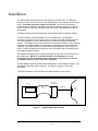
The IP-Ethernet is a two-board set consisting of a single-wide IndustryPack and one of
three available transition modules. Interconnection between the two boards is
accomplished by a 50-pin ribbon cable. Figure 1 below illustrates the typical
arrangement of IP, Carrier board and transition module.
Figure 1 below shows the typical arrangement of IP, Carrier board, and Transition
Module. The ribbon cable is a 50-pin cable and can be a maximum of six feet in length.
IP-Ethernet
Ribbon
Cable
Transition
Module
IP Carrier
Figure 1
Typical Arrangement of IP, Carrier Board, and Transition Module
The IP portion of IP-Ethernet contains three principle elements plus driver / receiver
circuitry. A block diagram of the IP is shown in Figure 2.
The "core" element of the IP, the LANCE chip, is a 48-pin VLSI CMOS device which
provides a complete interface module enabling the host to access the Ethernet network.
Specific functions provided by the LANCE, applicable to IP-Ethernet include slave
parallel bus interface, serial I/O interface, station address detection, on-board DMA,
advanced buffer management, error reporting and retry, and diagnostics.
16 Kbytes of static RAM is provided for storage of send and receive packets.
5
LANCE
Rx
RClk
Tx
TClk
74ACT245
AM7990
Logic
Interface
LCA
SRAM
XC3030
16 KB
8
Figure 2
Block Diagram of IP Portion of IP-Ethernet
A field programmable Xilinx XC3030 Logic Cell Array (LCA) contains the IP interface
logic as well as other miscellaneous control functions. A control and status register is
provided for interrupt processing and transition module identification. An eight-bit
interrupt vector register stores the pointer to the interrupt service routine. The standard
IP ID PROM is also implemented in the LCA. Two additional registers are included for
programming the LANCE chip.
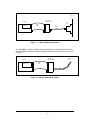
The IP-Ethernet Transition Module (XM) comes in three versions. Connectability to
10Base5 (Ethernet) is provided by the IP-Ethernet XM-10Base5 (AUI) transition module.
Connectability to 10Base2 (Cheapernet) networks is provided by the IP-Ethernet XM10Base2 transition module (Figure 3). Connectability to 10-BaseT(Twisted Pair)
networks is provided by the IP-Ethernet XM-10BaseT transition module (Figure 4).
All versions of transition modules contain an Am7992 Serial Interface Adapter (SIA). The
Am7992 provides three basic functions. It is a Manchester Encoder/line driver in the
transmit path, a Manchester Decoder with noise filtering and quick lock-on
characteristics in the receive path, and a signal detect /converter (10 Mhz. differential to
TTL) in the collision path. In addition, the SIA provides the interface between the TTL
logic environment of the IP and the differential signaling environment in the network
cable.
6
Rx
RClk
SIA
Tx
Rcv +
Rcv -
DI -
Coll +
CI +
Coll -
CI -
Xmit +
TClk
DI +
Xmit -
Coax
Intfc
DO +
DO Am7996
Am7992B
Figure 3
XCVR
IP-Ethernet Transition Module XM-10Base2 (Coax)
The IP-Ethernet XM-10Base2 supports one network attachment configurations,
10-Base2(Cheapernet) . It contains an Am7996 IEEE 802.3/Ethernet/Cheapernet
Transceiver. When used in a 10-Base2(Cheapernet) configuration, this device performs
transmit, receive, and collision detect functions at the coaxial media interface and
provides translation to differential signals which are coupled to the Am7992 SIA
interface through isolation transformers. The network interface of the Am7996 connects
externally through an RG58 coaxial BNC connector.
The 10-Base5(Ethernet) transition module does not use the Am7996. The function
provided by the Am7996 is provided by a Medium Attachment Unit(MAU) which is
external to the transition module. Access to the MAU occurs over an Attachment Unit
Interface(AUI) cable, one end of which connects to a 15 pin D shell connector mounted
on the transition module. The connector is connected on the transition module directly to
the Am7992 SIA, creating a bypass around the on-board isolation transformers and
Am7996. In this configuration, isolation from the network is provided by the MAU.
7
Rx
RxD+
RD+
RxD-
RD-
TxD+
TD+
TxD-
TD-
Rcv +
XCVR
SIA
RClk
Rcv Coll +
Coll -
Tx
Twisted Pair
Interface
Xmit +
TClk
Xmit -
Am7992B
Figure 4
Am7998
IP-Ethernet Transition Module XM-10BaseT (Twisted Pair)
The IP-Ethernet XM-10BaseT supports the 10-BaseT(Twisted Pair) configuration. It
contains an Am79C98 Twisted Pair Ethernet Transceiver(TPEX). This device provides
Twisted Pair driver and receiver circuits including on-board transmit digital pre-distortion
and receiver squelch. The TPEX is interfaced directly to the Am7992 Serial Interface
Adapter. Twisted Pair Receive Polarity Detection and Automatic Polarity Reversal and
Link Status Indication is also provided. LEDs are connected to these pins. The network
transmit path includes a discrete resistor circuit, filter, and pulse transformer. The
network receive path consists of pulse transformer, filter, and termination resistor. The
differential transmit and receive signals connect externally through an RJ45 connector.
This transition module does not support an MAU/AUI configuration.
Caution: The transition module provides the clock to the Lance chip. If no transition
module is installed, then the RDP and RAP registers in the Lance chip are not functional
and a bus error is likely to result. To avoid this error, check the [3..2] bits in the Status
Register prior to accessing the RDP or RAP.
8
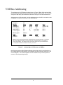
VMEbus Addressing
The address map for IP-Ethernet is shown below in Figure 5. Both 16-bit word and 8-bit
byte accesses are supported. Byte accesses are mapped to data line D0..D7. This is the
odd byte in 68K family host architectures and the even byte in Intel host architectures.
Addresses are not fully decoded. Only the addresses shown should be accessed or data
may appear in more than one place in the address space.
I/O Space
Register
RDP Register
RAP Register
Vector Register
Status Register
Control Register
I/O
Offset
$00
$02
$41
$43
$43
Memory Space
RAM
RAM start
RAM end
Memory
Offset
$0000 to
$3FFF
Mode
R/W
R/W
R/W
R
W
Width
word
word
byte
byte (4 bits)
byte (2 bits)
Mode
R/W
Width
byte
or word
Notes
In Lance chip
In Lance chip
Note 1
Note 1
Note 1
Notes
Memory
Space
Note 1: The Vector Register must be initialized prior to normal operation. The Status
and Control Register must be accessed each time by the interrupt service routine to
clear each interrupt. The Status Register should be checked on system initialization
to verify that a transition module is correctly connected.
Figure 5
Address Map of IP-Ethernet, on VMEbus
Note that previously existing Ethernet software drivers that use the Lance chip have to
be modified slightly for the specifics of this address map and interrupt control bits in the
Control Register. The Control Register must be accessed once per interrupt service
routine to clear the pending interrupt.
9
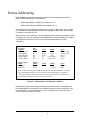
Nubus Addressing
NuBus addressing requires computing the address from the addresses given above
under VMEbus addressing. The formulas are:
NuBus byte address = (VMEbus byte address * 2) + 1
NuBus word address = (VMEbus word address * 2) + 2
The address map for IP-Ethernet is shown below in Figure 6. Both 16-bit word and 8-bit
byte accesses are supported. Byte accesses are mapped to data line D0..D7; word data
is mapped to data lines D0..D15.
Addresses are not fully decoded. Only the addresses shown should be accessed or data
may appear in more than one place in the address space. Interrupt mapping is a function
of the selected carrier board. See your IP carrier board User Manual for more
information.
I/O Space
Register
RDP Register
RAP Register
Vector Register
Status Register
Control Register
I/O
Offset
$02
$06
$83
$87
$87
Memory Space
RAM
RAM start
RAM end
Memory
Offset
$0000 to
$7FFF
Mode
R/W
R/W
R/W
R
W
Width
word
word
byte
byte (4 bits)
byte (2 bits)
Mode
R/W
Width
byte
or word
Notes
In Lance chip
In Lance chip
Note 1
Note 1
Note 1
Notes
Memory
Space
Note 1: The Vector Register must be initialized prior to normal operation. The Status
and Control Register must be accessed each time by the interrupt service routine to
clear each interrupt. The Status Register should be checked on system initialization
to verify that a transition module is correctly connected.
Figure 6
Address Map of IP-Ethernet, on Nubus
Note that previously existing Ethernet software drivers that use the Lance chip have to
be modified slightly for the specifics of this address map and interrupt control bits in the
Control Register. The Control Register must be accessed once per interrupt service
routine to clear the pending interrupt.
10
ISA (PC-AT) Bus Addressing
ISA (PC-AT) addressing requires computing the address from the addresses given
above under VMEbus addressing. The formulas are:
ISA Bus byte address = VMEbus byte address - 1
The address map for IP-Ethernet is shown below in Figure 7. Both 16-bit word and 8-bit
byte accesses are supported. Byte accesses are still mapped to data line D0..D7. There
is no change to word data address mapping.
Addresses are not fully decoded. Only the addresses shown should be accessed or data
may appear in more than one place in the address space. Interrupt mapping is a function
of the selected carrier board. See your IP carrier board User Manual for more
information.
I/O Space
Register
RDP Register
RAP Register
Vector Register
Status Register
Control Register
I/O
Offset
$00
$02
$40
$42
$42
Memory Space
RAM
RAM start
RAM end
Memory
Offset
$0000 to
$3FFF
Mode
R/W
R/W
R/W
R
W
Width
word
word
byte
byte (4 bits)
byte (2 bits)
Mode
R/W
Width
byte
or word
Notes
In Lance chip
In Lance chip
Note 1
Note 1
Note 1
Notes
Memory
Space
Note 1: The Vector Register must be initialized prior to normal operation. The Status
and Control Register must be accessed each time by the interrupt service routine to
clear each interrupt. The Status Register should be checked on system initialization
to verify that a transition module is correctly connected.
Figure 7
Address Map of IP-Ethernet, on ISA (PC-AT) Bus
Note that previously existing Ethernet software drivers that use the Lance chip have to
be modified slightly for the specifics of this address map and interrupt control bits in the
Control Register. The Control Register must be accessed once per interrupt service
routine to clear the pending interrupt.
11
Installation
The IndustryPack operates with one of two transition modules (XM). The Selected
transition module connects to the IP via a standard 50-pin ribbon cable to the IP carrier
board. This cable may be any length up to six feet. This permits mounting the
transition module wherever convenient for the OEM or systems integrator. It does not
have to reside in a VME slot, although a VME front panel is provided with the XM for
convenience.
A transition module and 50-pin data cable is provided with each IP-Ethernet ordered.
Transition modules may be mounted in 3U or 6U VMEbus slot. No backplane
connection is required, so the module is often mounted in the VME cardcage past the
end of the backplane, so that it does not take up a relatively expensive backplane
position. The module may be removed from the front panel provided for easy mounting
elsewhere in the OEM's system. The XM modules are designed to be built with either
straight or right-angle connectors to permit more mounting options, such as flush to a
panel. Contact GreenSpring Computers for more information about mounting options
and custom transition modules.
The transition modules for the IP-Ethernet provide the main clock to the Lance chip on
the IndustryPack. NOTE: If a transition module is not installed (or it is not
connected to the IP carrier board) then the registers on the Lance chip are not
accessible to the host, and a "bus error" may result.
The XM-10Base2 transition module allows attachment to a coax Ethernet system. The
XM-10Base2 features the BNC connector , see Figure 8 used for a direct coax
connection.
For DB15 connector for AUI and thick wire implementations, see Figure 9.
XM 10Base 2
TransitionModule
IP Carrier
Ribbon
Cable
IP-Ethernet
Figure 8
RG58 Coax
10Base2 Attachment Scheme
12
RG58
BNC "T"
Ethernet
Coax
XM 10Base 2
TransitionModule
IP Carrier
IP-Ethernet
Hot
Tap
Ribbon
Cable
Figure 9
AUI
Cable
10Base5 Attachment Scheme
The XM-10BaseT transition module permits attachment to a twisted-pair Ethernet LAN.
The XM-10BaseT features an industry standard modular connector for ease of use. See
Figure 14.
XM 10Base T
Transition Module
IP Carrier
IP-Ethernet
Ribbon
Cable
Figure 10 10BaseT Attachment Scheme
13
Twisted
Pair
Theory Of Operation
This section contains a discussion of Local Area Network (LAN) technology in general,
including background information relating specifically to Ethernet/IEEE 802.3. The
various media supported by Ethernet and how those are each addressed by the
GreenSpring IP-Ethernet module set are then discussed. Finally, the functional
characteristics specific to the GreenSpring IP-Ethernet module set are described in
detail.
LAN Overview
A local area network (LAN) is a data communication facility providing high-speed
switched connections between processors, peripherals, and terminals within a single
building or campus. Historically, LANs have evolved from the data processing or office
processing industry where economics suggest relatively expensive storage devices and
printers should be shared by multiple computers. Thus, LANs have evolved partly in
response to the emergence of low-cost computing and it's need for high-cost peripherals.
Indeed, the first generation LANs were actually one form of distributed computer
systems using proprietary high-speed data links between processing nodes and
peripheral equipment. The capabilities of a typical LAN represent a compromise between
long distances and wide bandwidth.
IEEE 802.3 is an international standard for local area networks which specifies the
carrier sense multiple access with collision detection (CSMA/CD) access method and
physical layer. It includes specific media attachment types 10Base5, 10Base2, and
10BaseT among others.
Ethernet, a registered trademark of the Xerox Corporation, is defined by IEEE 802.3 as
media type 10Base5. It represents the first major product offering with non-proprietary
communications interfaces and protocols. The architecture is based in concept on that of
a satellite communications network which allows multiple distributed devices to
communicate with each other over a single radio channel using a satellite as a
transponder. One station communicates with another by waiting until the radio channel is
idle (determined by carrier sensing) and then sending a packet of data with a destination
address, source address, and redundant check bits to detect transmission errors. All idle
stations continuously monitor incoming data and accept those packets with their address
and valid check sums. Whenever a station receives a new packet, the receiving station
returns an acknowledgment to the source. If an originating station receives no
acknowledgment within a specified time interval, it re-transmits the packet under the
assumption that the previous packet was interfered with by noise or by a transmission
from another station at the same time. (The latter situation is referred to as a collision.)
The Ethernet employs the same basic system concept using coaxial cable or twisted pair
distribution throughout a building or campus.
The transmission media of the Ethernet is a coaxial or twisted pair cable using baseband
transmission at 10 Mbs. Baseband transmission implies data is transmitted without the
use of a carrier and with only one channel defined in the system. Data is encoded using
a Manchester code. This code provides a strong timing component for clock recovery
because a timing transition always occurs in the middle of every bit. The Manchester line
code has the additional property of always maintaining equal amounts of positive and
negative voltages. This prevents the build-up of a DC component which simplifies the
implementation of decision thresholds in the data detectors.
14
Although the data is not transmitted with a carrier per se, the continuous transitions of
the Manchester code provide the equivalent of a carrier so the channel is easily
monitored for activity by the equivalent of a carrier sense. Multiple access to the coaxial
cable is provided by passive taps, thereby allowing station connections to be added or
removed without disrupting traffic in the system.
Another requirement of the transmission link and it's associated access electronics is
that, while transmitting, a transceiver must be capable of detecting the existence of
another active transmitter. This is referred to as collision detection. Thus, the three basic
steps for accessing an Ethernet are denoted CSMA/CD for: Carrier Sense, Multiple
Access with Collision Detection.
The ability to detect collisions allows colliding stations to release the channel after using
it for only a short period of time. Because carrier presence is checked before
transmitting, collisions occur only if two stations begin transmitting within a time interval
equal to the propagation delay between two stations. By restricting the maximum
distance between transceivers to 2500 meters, the collision window is limited to 23 µsec
including amplifier delays.
Once a station begins transmitting, it can be sure that no collision will occur if none is
detected within a round-trip propagation time of 46.4 µsec. Since one bit time is 100 ns
at 10 Mbs, the collision detection decision is made within 464 bit times. The maximum
length of a frame is 12,144 bits, thus the collision detection feature will detect a collision
very early in the frame to save significant transmission time that would be wasted if the
entire frame were transmitted before detection.
Whenever a collision occurs, all colliding stations detect the condition and wait
individually random amounts of time before retrying the transmission. By waiting random
amounts of time before transmitting, the probability of repeated collisions is reduced. In
heavy traffic conditions, the average delay before re-transmission begins to increase
after 10 unsuccessful attempts. After 16 collisions, no further attempts are made to
transmit that message and the station is notified of the error by the transceiver.
Media
The original Ethernet configuration consisted of multiple distributed devices (DTE's)
communicating over single 0.4 inch "thickwire" coaxial cable "media" distributed
throughout a building or campus. Access by DTE's to the coaxial cable is provided by
Media Attachment Unit (MAU) modules which physically mount directly on the cable.
The modules consist of transceiver circuits, collision detection circuits, "Jabber"
controllers which prevent the DTE from transmitting excessively, and isolating pulse
transformers which connect directly to the Attachment Unit Interface (AUI) cable
connector. The AUI cable has 15-pin D-shell connectors (MIL-C-24308 or equivalent) at
each end. The tap has a male connector while the DTE station apparatus has a female
connector, thus the interconnecting cable must have one of each type. The pin
assignments are:
1.
2.
3.
4.
5.
6.
7.
Shield
Collision Presence +
Transmit +
Reserved
Receive +
Power Return
Reserved
8.
9.
10.
11.
12.
13.
14.
15.
15
Reserved
Collision Presence–
Transmit–
Reserved
Receive–
Power
Reserved
Reserved
This configuration is now referred to as 10Base5 (Ethernet) and is supported by IPEthernet. It requires a user provided AUI and IP-Ethernet (LANCE)-AUI must be
specified when ordering.
A second coaxial cable configuration, 10Base2 - "cheapernet", emerged which uses
RG58 type cable, a much more common and less expensive cable technology than the
original "thickwire". In cheapernet applications, the Media Attachment Unit typically
resides inside the DTE with its signals to the DTE isolated and the (0.2" diameter ) media
directly connected to the DTE. This configuration is supported by IP-Ethernet. Specify
IP-Ethernet (LANCE)-TPair when ordering.
Transceiver power and ground in both applications are isolated from that of the DTE.
The Ethernet/IEEE 802.3 10BaseT standard provides for attachment to Twisted Pair
Medium. A network based on this standard can use unshielded twisted pair cables, thus
providing an economical solution to networking by allowing the use of existing telephone
wiring. 10BaseT standard supports a star-wired physical network configuration rather
than the traditional multidrop topology. As such, all DTE's connect point-to-point to a
central Repeater which performs arbitration and node connection. In Twisted Pair
applications, the Media Attachment Unit may reside inside the DTE or may be accessed
remotely by way of an Attachment Unit Interface cable. The IP-Ethernet only supports
configurations in which the MAU resides inside the DTE.
16
Functional Description
IP-Ethernet consists of the following functional blocks:
LANCE Controller
Serial Interface Adapter (SIA)
Transceiver
RAM
Arbiter
Interrupt Logic
IP Interface Logic
These blocks combine to provide full DTE functionality for all supported configurations.
Additionally, for 10Base2 and 10BaseT configurations they provide MAU functionality as
well.
Function select logic, arbiter, interrupt logic and IP interface logic is all located in a 100pin Xilinx programmable logic cell array (LCA). There are also two registers in the Xilinx
LCA. One register is used for control and status and the other is an eight-bit interrupt
vector register.
Controller
The basic operation of the LANCE consists of two distinct modes: transmit and receive.
In the transmit mode the LANCE chip directly accesses data in a transmit buffer in RAM.
It prefaces the data with a preamble, sync pattern, and calculates and appends a 32-bit
CRC. On transmission, the first byte of data loads into a 48-byte FIFO. The LANCE then
begins to transmit the preamble while simultaneously loading the rest of the packet into
the FIFO for transmission.
In the receive mode, packets are sent via the SIA to the LANCE. The packets are loaded
into the 48-byte FIFO for preparation of automatic downloading into a receive buffer
located in RAM. A CRC is calculated and compared with the CRC appended to the data
packet. If the calculated checksum doesn't agree with the packet CRC, an error bit is set.
Serial Interface Adapter (SIA)
The Serial Interface Adapter has three basic functions. It is a Manchester Encoder/line
driver in the transmit path, a Manchester Decoder with noise filtering and quick lock-on
characteristics in the receive path, and a signal detect/converter (10 Mhz. differential to
TTL) in the collision path. In addition, the SIA provides the interface between the TTL
logic environment of the LANCE and the differential signaling environment in the
transceiver cable.
The transmit section encodes separate clock and NRZ data input signals meeting
specific set-up and hold time requirements into a standard Manchester II serial bit
stream.
In the receive path, the SIA signals the LANCE that there is information on the receive
signal pair, and separates the incoming Manchester-encoded data into clock and NRZ
data.
Transceiver
Four functions are provided by the transceiver. When transmitting it receives signals
from the SIA and sends them to the coaxial or twisted pair medium. When receiving it
17
obtains data from the media and sends it to the SIA. It also provides Collision Detect
capability in which it notifies the SIA if a collision has occurred on the media. In addition,
it provides Jabber protection by guarding the medium from transmissions which are
excessive in length.
RAM
Dual port static RAM is provided for storage of send and receive packets. RAM capacity
is 16 Kbytes. Transfer of data between the memory and the SIA is under control of a
DMA controller located internally on the LANCE chip.
RAM can also be accessed by the host processor from the IP Logic Interface. The arbiter
selects between the host and the Lance for access to the RAM at a given time. The host
and Lance bus response signals are delayed until the arbiter grants access to that
memory port. There are a variable number of IP wait states for the host port. The
maximum delay is set by the Lance, about one microsecond.
The host places a message to be transmitted into the RAM and sets the Lance protocol
flags. The Lance polls the memory and determines that the message to be transmitted
is present, begin to read the message into the Lance and prepare for transmission. The
host will have previously set-up the message passing memory organization through a
series of descriptor words located in the RAM and pointed to by the Lance control
registers. Please refer to the AMD Lance data book contained in GreenSpring
Computer's Engineering Kit for more information.
Arbiter
The RAM interface is controlled by the ARBITER which is an XABLE logic block. The
Arbiter is a one-bit implementation which looks at requests from the Host and from the
Lance and determines which port has access to the memory. The request from the
Lance is asynchronous to the IP Clock. The Arbiter double clocks the request from the
Lance to make sure that the Arbiter is not operating on a metastable condition. Enable A
is the enable to the host port and is active any time that the Lance is not the master or
requester. Enable B is the grant to the Lance and is active when the Lance requests the
memory and the Host is not already using it.
Interrupts
All IndustryPack interrupts use a vector. The vector from the IP-Ethernet comes from a
vector register loaded as part of the initialization process. The vector register can be
programmed to any 8 bit value. The default value is $FF which is usually not a valid
user vector. The software is responsible for choosing a valid user vector.
Interrupts can be generated from a number of causes. The Lance chipset provides a
global interrupt enable bit. As part of the interrupt service routine the status register is
read to determine the cause of the interrupt. The Lance provides six types [causes] of
interrupt. The interrupts can occur in parallel -- more than one source at a time. All of
the interrupt types should be tested as a part of each interrupt service routine. The
Lance can generate interrupts to indicate that a message has been sent [TINT], received
[RINT], Transmitter time-out error [BABL], Memory time-out error [MERR], Missed
packet [MISS], and Initialization Done [IDON], Please refer to the Lance data book for
more information.
A second source of interrupts is used for test purposes. The control register contains an
INTSET bit which creates an interrupt request when set to one. The interrupt request
18
remains enabled until the INTSET bit is rewritten to zero.
Interface Logic
The interface logic on the IP-Ethernet consists of the ID PROM, decoder and some
control logic. This logic implements the address map for the I/O Space resources
including the RDP Register, RAP Register, Vector Register, and Control and Status
Register; and provides chip select to the dual port RAM when a memory select is
detected from the host.. It generates the necessary control signals on the IP. It generates
zero or multiple wait states as required during accesses. All of these functions are
implemented in a single Xilinx logic cell array (LCA).
19
Programming
Control and Status Register
The control and status register is the same register. It is called the Control Register for
write operations, where there are two effective bits. It is called the Status Register for
read operation, where there are four effective bits.
The two bits in the Control Register control the interrupt from the IP. This Register must
be initialized prior to interrupt operation and must also be written to every interrupt to
clear the pending interrupt. The six high order bits are "don't care" on writes, but setting
these bits to zero is recommended for consistency. These two bits read back as written
in the Status Register. They are cleared to zero on Reset.
Bit [0] must be set to one to enable interrupts. It must be toggled to zero then back to
one by the interrupt service routine to clear each pending interrupt.
Bit [1] must be set to zero for normal operation. Setting this bit to one will force an
interrupt, even if bit [0] is at zero. This feature may be used to test interrupts without
involving the Lance chip or any network interaction.
There are four effective bits in the Status Register. The two low bits read back as
written from the Control Register. Bits [3.2] provide a static code that indicates which, if
any, transition module is installed. These bits should be checked during system
initialization and an appropriate error message generated if they are not set as expected.
High order bits [7..4] do not read back predictably and should be masked off and
ignored by the programmer.
Caution: The transition module provides the clock to the Lance chip. If no transition
module is installed, then the RDP and RAP registers in the Lance chip are not functional
and a bus error is likely to result. To avoid this error, check the [3..2] bits in the Status
Register prior to accessing the RDP or RAP.
The control port is read-writable. The control port, when written to, controls the interrupt
enable and interrupt set bits. The read operation accesses the interrupt control bits plus
the connection status from the expansion boards. The port is initialized to 0 with reset.
The Control and Status Register is implemented internally within the Xilinx LCA.
20
Bit
[0]
[1]
[3..2]
Function
Interrupt enable
0 = interrupt disabled
1 = interrupt enabled
Interrupt Force
0 = normal operation
1 = force interrupt on
00 = Coax TM installed
01 = (spare)
10 = Twisted Pair TM installed
11 = no transition module installed
Note: Bit [0] should be toggled 1 -> 0 ->1 by the interrupt
service routine to clear each pending interrupt.
Note: Mask off high order bits when reading. Bits [7..2]
are "don't care" on writes.
Figure 11 Control and Status Register
Vector Register
The 8-bit Vector Register is used by the software to store the pointer to the interrupt
service routine associated with the IP-Ethernet's driver. The interrupt vector is set to
$FF during Reset. This host software must initialize this register prior to enabling
interrupts. The vector register is read-writable in the I/O space. The vector register is
implemented within the Xilinx LCA..
RAM
The IP-Ethernet provides 16 Kbytes of static RAM for storage of send and receive
packets. This RAM should generally be initialized (or cleared) following Reset by the
driver software to assure consistent operation.
The most common packet size on TCP/IP 802.1 networks is 1K bytes. The dual-port
memory is thus large enough for 16 of these common packets. However, it is necessary
to use some of the memory capacity for overhead, therefore, taking this into account,
actual packet capacity would be limited to fifteen packets. In most implementations the
host software will not use this memory for long term packet storage but will load and
unload packets expeditiously.
The Lance chip has an internal DMA controller for transferring data to and from the
memory on the IP during transmission.
The host will place a message to be transmitted into the RAM and set the Lance protocol
flags. The Lance will poll the memory and determine that the message to be transmitted
is present, begin to read the message into the Lance and prepare for transmission. The
host will have previously set-up the message passing memory organization through a
series of descriptor words located in the RAM and pointed to by the Lance control
registers. Please refer to the AMD Lance data book contained in GreenSpring
Computer's Engineering Kit for more information.
21
The host can read or write to the RAM at any time because the Xilinx device contains an
arbiter to select between the host and the Lance for ownership of the RAM at a given
time. The host and Lance have their bus response signals delayed until the arbiter
grants access to that memory port. There are a variable number of IP wait states for the
host port. The maximum delay is set by the Lance, about one microsecond.
Register Data Port [RDP]
The Lance chipset is programmed through the Register Data Port (RDP). There are four
control and status ports accessed through the RDP. The RAP selects which CSR the
RDP will access. CSR 0 is the general control port with control over interrupt generation,
initialization, and status from the interrupt and error sources. CSR 1 contains the
address in RAM of the initialization block. CSR2 contains the upper 8 addresses of the
initialization block. CSR3 contains a four bit port to define the type of Bus Master
interface is to be implemented.
Please refer to the AMD handbook on the Lance chip-set for more information. A copy is
contained in the IP-Ethernet Engineering Kit from GreenSpring Computers.
Register Address Port [RAP]
The Register Address Port (RAP) is utilized to select which CSR that the RDP points to.
The Lance uses a windowing scheme to interface the CPU to the internal registers. The
RAP controls the window.
Please refer to the AMD handbook on the Lance chip-set for more information. A copy is
contained in the IP-Ethernet Engineering Kit from GreenSpring Computers.
22
IndustryPack I/O Interface Pin Assignment
The figure below gives the pin assignments for the IndustryPack I/O Interface from the
IP to the Transition Module. Users do not normally have to be concerned with this
interface unless they are designing their own transition module. See the section on
Installation for more information about wiring to the user network.
GND
GND
Rx
GND
GND
Rclk
GND
GND
Tx
GND
GND
Tclk
GND
GND
CLSN
GND
GND
TENA
-12V
-12V
-12V
-12V
+12V
+12V
GND
GND
+5V
+5V
+5V
+5V
GND
GND
B0
GND
B1
GND
Reset*
GND
GND
GND
GND
GND
GND
GND
GND
RENA
GND
+12V
+12V
GND
1
26
2
3
27
28
4
5
29
30
6
7
31
32
8
9
33
34
10
11
35
36
12
13
37
38
14
15
39
40
16
17
41
42
18
19
43
44
20
21
45
46
22
23
47
48
24
25
Figure 12 IP Interface to Transition Module Pin Assignment
23
49
50
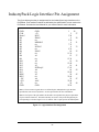
IndustryPack Logic Interface Pin Assignment
The figure below gives the pin assignments for the IndustryPack Logic Interface on the
IP-Ethernet Pins marked n/c below are defined by the specification, but not used on the
IP-Ethernet See also the User Manual for your carrier board for more information.
GND
CLK
Reset*
D0
D1
D2
D3
D4
D5
D6
D7
D8
D9
D10
D11
D12
D13
D14
D15
BS0*
BS1*
–12V
+12V
+5V
GND
GND
+5V
R/W*
IDSel*
n/c
MEMSel*
n/c
INTSel*
n/c
IOSel*
n/c
A1
n/c
A2
n/c
A3
INTReq0*
A4
n/c
A5
n/c
A6
Ack*
n/c
GND
1
2
3 28
4
5 30
6
7 32
8
9 34
10
11 36
12
13 38
14
15 40
16
17 42
18
19 44
20
21 46
22
23 48
24
25 50
26
27
29
31
33
35
37
39
41
43
45
47
49
Note 1: The no-connect signals above are defined by the IndustryPack Logic Interface
Specification, but not used by this IP. See the Specification for more information.
Note 2: The layout of the pin numbers in this table corresponds to the physical placement
of pins on the IP connector. Thus this table may be used to easily locate the physical pin
corresponding to a desired signal. Pin 1 is marked with a square pad on the IndustryPack.
Figure 13 Logic Interface Pin Assignment
24
Transition Module Pin Assignments
IP Interface
The figure below gives the transition module pin assignments for the I/O Interface from
the IP to the transition module. More specifically, it is the signal interface between the
7990 LANCE chip on the IP and the 7992 Serial Interface Adapter chip on the transition
module. It applies to both the XM-10Base2 and XM-10BaseT transition modules.
Pin
Signal Name
Pin
Signal Name
1
2
3
4
5
6
7
8
9
10
11
12
13
14
15
16
17
18
19
20
21
22
23
24
25
GND
GND
Rx
GND
GND
Rclk
GND
GND
Tx
GND
GND
Tclk
GND
GND
CLSN
GND
GND
TENA
–12V
–12V
–12V
–12V
+12V
+12V
GND
26
27
28
29
30
31
32
33
34
35
36
37
38
39
40
41
42
43
44
45
46
47
48
49
50
GND
+5V
+5V
+5V
+5V
GND
GND
B0
GND
B1
GND
Reset* (note 2)
GND
GND
GND
GND
GND
GND
GND
GND
RENA
GND
+12V
+12V
GND
Notes:
1. All signals are standard TTL logic voltage levels.
2. This signal is not used on XM-10Base2.
Figure 14 Transition Module IP Interface Pin Assignment
25
Attachment Unit Interface
The Attachment Unit Interface (AUI) is only provided on the XM-10Base2 Transition
Module and only applies to 10Base5 configurations. This interface provides for
connection to a user provided Media Attachment Unit (MAU) which has been mounted
directly to an Ethernet "thickwire" coax.
Pin
1
2
3
4
5
6
7
8
Signal Name
Pin
Signal Name
GND
Clsn+
Tx+
GND
Rx+
GND
n/c
GND
9
10
11
12
13
14
15
Clsn–
Tx–
GND
Rx–
+12V (Note 1)
GND
GND
Notes:
1. This voltage is fused.
Figure 15 XM-10Base2 Transition Module AUI Interface Pin Assignment
Coax Interface
The Coax Interface is only provided on the XM-10Base2 Transition Module and only
applies to XM-10Base2 "cheapernet" configurations. This interface provides for a "T"
connection to an RG58 BNC "T" adapter.. The board mounted connector is a standard
coaxial BNC female connector with the center conductor going to both receive data and
transmit data pins on the 7996 transceiver chip. The outer conductor goes to an isolated
shield circuit.
Twisted Pair Interface
The Twisted Pair Interface is only provided on the XM-10BaseT Transition Module and
only applies to 10BaseT twisted pair configurations. This interface provides for a point to
point connection to a twisted pair hub.. The board mounted connector is an RJ45 eight
position connector. Pin assignments are as indicated in the figure below.
Pin
1
2
3
4
Signal Name
TD+
TD–
RD+
n/c
Pin
5
6
7
8
Signal Name
n/c
RD–
n/c
n/c
.
Figure 16 XM-10BaseT Transition Module Twisted Pair Interface Pin Assignment
The five LEDs on the transition module provide the following status.
LED 1, Collision - The IP-Ethernet was transmitting data at the same time data
was being received.
LED 2, Receive - The IP-Ethernet is receiving data.
LED 3, Transmit - The IP-Ethernet is transmitting data.
26
LED 4, Link Polarity - If this LED is ON the Link Polarity is correct otherwise the
Link Polarity is reversed indicating that there is a wiring error.
LED 5, Link Status - If this LED is ON the Link is up and functional.
27
ID PROM
Every IP contains an IP PROM, whose size is at least 32 x 8 bits. The ID PROM aids in
software auto configuration and configuration management. The user's software, or a
supplied driver, may verify that the device it expects is actually installed at the location it
expects, and is nominally functional. The ID PROM contains the manufacturing revision
level of the IP. If a driver requires that a particular revision be present, it may check for
it directly.
As with all Ethernet controllers, each IP-Ethernet LANCE has a unique destination
address associated with it. This 48-bit number provides a mechanism for routing
packets to the appropriate node on a LAN.
The ID PROM of the IP-Ethernet LANCE is large enough to conveniently support only 32
bits of this 48-bit address. Fortunately, the remaining 16 bits of the address are
constant, since they comprise part of the unchanging manufacturers code. Therefore,
by knowing this invariant part of the address and combining it with the unique
information in the ID PROM, the full Ethernet address may be obtained. Refer to the
IndustryPack Specification for more information about the ID Space, and to the
documentation for your carrier board for information concerning the starting address for
this Space.
The Ethernet address is typically written as a 12-digit hexadecimal number. The first
four digits of this number for all Ethernet products manufactured by GreenSpring
Computers are 2E45. This is the invariant portion of the address that does not appear in
the ID PROM. It is typically hard coded into any drivers for the IP-Ethernet LANCE.
The remaining eight hexadecimal digits are stored in the ID PROM as binary numbers.
The next two digits after 2E45 are stored in the byte at offset $19 (on VMEbus carrier
boards) from the beginning of the ID PROM. Again, this is an unsigned binary number,
and not an ASCII representation of the hex digits. The next two digits are at offset $1B,
the next two at $1D, and the final digits are at offset $1F from the beginning of the ID
PROM.
The following table shows how the example Ethernet address 2E45 EFF9 D744 would be
stored in the IP-Ethernet LANCE:
Ethernet Node Address
2E <47:40>
45 <39:32>
EF <31:24>
F9 <23:16>
D7 <15:08>
44 <07:00>
Storage Location in ID PROM
None (Implied)
None (Implied)
ID PROM Base Address + $19
ID PROM Base Address + $1B
ID PROM Base Address + $1D
ID PROM Base Address + $1F
Note that the ID PROM CRC and Size fields do reflect the presence of the addressing
information stored in the ID PROM.
28
Data in the ID PROM, including the variable 32-bit portion of the Ethernet address, is
shown below. For more information on IP ID PROMs refer to the IndustryPack® Logic
Interface Specification, available from GreenSpring Computers and other sources.
The ID PROM used is internal to the Xilinx logic device on the IP-Ethernet [Lance].
3F
21
1F
1D
1B
19
17
15
13
11
0F
0D
0B
09
07
05
03
01
Ethernet Address bits <07:00>*
Ethernet Address bits <15:08>*
Ethernet Address bits <23:16>*
Ethernet Address bits <31:24>*
CRC
No of bytes used
Driver ID, high byte
Driver ID, low byte
reserved
Revision
Model No IP-Ethernet
Manufacturer ID GreenSpring
ASCII "C"
ASCII "A"
ASCII "P"
ASCII "I"
(44)
(D7)
(F9)
(EF)
(0C)
(00)
(A1)
(35)
(F0)
(43)
(41)
(50)
(49)
Figure 17 ID PROM Data
* NOTE:
These fields are variable for each IP; the values shown here are for
illustration purposes only.
The below example represents how the contents of the above example ID PROM might
appear when displayed by a debugger.
RomBug: d ffd080
0x00FFD080
- FF49FF50 FF41FF43 FFF0FF35 FFA1FF00
0x00FFD090
- FF00FF00 FF10FFC3 FF EFFFF9 FFD7FF44
29
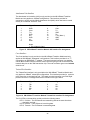
User Options (jumpers)
This section describes the shunts (jumpers) that are on the two transition modules.
There are no shunts on the IP.
Shunts for XM-10BaseT (Twisted Pair)
E1
Test input to 7992.
Normal = shunt out
E2
TSEL input to 7992
Normal = shunt n
E3
Test input to 79C98
Normal = shunt in
E4
SqeTest input to 79C98
Normal = shunt out
Shunts for XM-10Base2 (Coax)
E1
TSEL input to 7992
E2
Test input to 7992
E3
SqeTest input to 7996
Normal = shunt out
Normal = shunt out
Normal = shunt out
Shunts for XM-10Base5 (AUI)
E1
TSEL input to 7992
E2
Test input to 7992
Normal = shunt out
Normal = shunt out
Logic level low is achieved by installing a shunt.
Logic level high is achieved by removing a shunt.
TSEL [Transmit Mode Select] During idle transmit state with TSEL low transmit + is
positive with respect to transmit -. With TSEL high the transmit + is equal to transmit "zero" differential to operate transformer coupled loads.
Test [7992] high for normal operation, and low for testing of the receive path threshold
and RCLK output high parameters.
Test [79C98] High for loopback test mode. SqeTest determines type of loopback. Low
for normal operation.
SqeTest [Signal Quality Error Test (Heartbeat) Enable. When low (Station MAU), TPEX
transfers data independently from D0 to the TXD/TXP circuit and from RXD to the DI
circuit. If High (Repeater MAU) then data on the RXD circuit is transmitted back onto the
TXD/TCP circuit and data on the DO circuit is transmitted onto the DI pair.
30
Construction and Reliability
IndustryPacks were conceived and engineered for rugged industrial environments. The
IP-Counter is constructed out of 0.062 inch thick FR4 V0 material. The four copper
layers consist of two signal layers and two power and ground planes.
Through hole and surface mounting of components is used. IC sockets are screwmachined pins, gold plated. High insertion and removal forces are required, which
assists in keeping components in place. If the application requires unusually high
reliability or is in an environment subject to high vibration, the user may solder the four
corner pins of each socketed IC into the socket, using a grounded soldering iron.
The IndustryPack connectors are keyed, shrouded and gold plated on both contacts and
receptacles. They are rated at 1 Amp per pin, 200 insertion cycles minimum. These
connectors make consistent, correct insertion easy and reliable.
The IP is secured to the carrier with four metric M2 stainless steel screws. The heads of
the screws are countersunk into the IP. The four screws provide significant protection
against shock, vibration, and incomplete insertion. For most applications they are not
required.
The IndustryPack provides a low temperature coefficient of 0.89 W/°C for uniform heat.
This is based on the temperature coefficient of the base FR4 material of .31 W/m-°C,
and taking into account the thickness and area of the IP. This coefficient means that if
0.89 Watts is applied uniformly on the component side, that the temperature difference
between the component and the solder side is one degree Celsius.
31
Warranty and Repair
GreenSpring Computer warrants this product to be free from defects in workmanship and
materials under normal use and service and in its original, unmodified condition, for a
period of one year from the time of purchase. If the product is found to be defective
within the terms of this warranty, GreenSpring Computer's sole responsibility shall be to
repair, or at GreenSpring Computer's sole option to replace, the defective product. The
product must be returned by the original customer, insured, and shipped prepaid to
GreenSpring Computers. All replaced products become the sole property of GreenSpring
Computers.
GreenSpring Computer's warranty of and liability for defective products is limited to that
set forth herein. GreenSpring Computers disclaims and excludes all other product
warranties and product liability, expressed or implied, including but not limited to any
implied warranties of merchandisability or fitness for a particular purpose or use, liability
for negligence in manufacture or shipment of product, liability for injury to persons or
property, or for any incidental or consequential damages.
GreenSpring’s products are not authorized for use as critical components in life support
devices or systems without the express written approval of the president of GreenSpring
Computers, Inc.
Service Policy
Before returning a product for repair, verify as well as possible that the suspected unit is
at fault. Then call the Customer Service Department for a RETURN MATERIAL
AUTHORIZATION (RMA) number. Carefully package the unit, in the original shipping
carton if this is available, and ship prepaid and insured with the RMA number clearly
written on the outside of the package. Include a return address and the telephone
number of a technical contact. For out-of-warranty repairs, a purchase order for repair
charges must accompany the return. GreenSpring Computers will not be responsible for
damages due to improper packaging of returned items. For service on GreenSpring
Products not purchased directly from GreenSpring Computers contact your reseller.
Products returned to GreenSpring Computers for repair by other than the original
customer will be treated as out-of-warranty.
Out of Warranty Repairs
Out of warranty repairs will be billed on a material and labor basis. The current minimum
repair charge is $100. Customer approval will be obtained before repairing any item if
the repair charges will exceed one half of the quantity one list price for that unit. Return
transportation and insurance will be billed as part of the repair and is in addition to the
minimum charge.
For Service Contact:
Customer Service Department
GreenSpring Computers
1204 O’Brien Drive
Menlo Park, CA 94025
(415) 327-1200
(415) 327-3808 fax
32
Specifications
Logic Interface:
IndustryPack® Logic Interface 0.7.1 Compatible
Media Interface:
10Base2 (thin), 10Base5 (thick), 10BaseT (twisted pair),
Software Interface:
Control and Status Register
Vector Register
ID PROM
RAM
Lance Registers: RDP and RAP
Initialization:
Hardware Reset forces all registers to zero except
vector register which is initialized to $FF.
Access Modes:
Word or Byte in I/O Space (see memory map)
Word or Byte in ID Space
Byte in I/O Space to Lance Registers
Vectored interrupts
Word or Byte in Memory space
Wait States:
Zero1
Interrupt:
Multiple interrupts associated with the Lance and one for
hardware and software debugging created through the
control register.
DMA:
DMA is supported between the Lance chip and the
internal RAM.
Isolation Voltage
10Base2:
10Base5:
10BaseT:
Onboard Options:
All IP-Ethernet Options are Software Programmable
The Twisted pair and Coax expansion modules have
jumpers to select modes of operation..Please refer to
the Appendix for a list of options.
Interface Options:
50 pin flat cable to interconnect the IP-Ethernet Lance to
one of the Transition Modules. Coax [BNC, RG58]or
Twisted pair [RJ-45] to connect to the Ethernet LAN
Dimensions:
Standard Single IndustryPack.
1.8 x 3.9 x .344 (max) inches
Transition Modules
2.65 x 3.9 x .344(max) inches
(See drawing, last page this section.)
2000 VAC rms
Not Applicable2
500 VAC rms
1The
RAM access time may require wait-states if the RAM is being accessed by the network
when the Host begins a transfer cycle.
2Isolation is provided by Media Attachment Unit (MAU) which in this configuration is userprovided.
33
Construction:
Conformal Coated FR4 4 Layer Printed Circuit,
Through Hole and Surface Mount Components.
Programmable parts are socketed.
Temperature
Coefficient:
Power:
+5V @ 450 mA max [300 typ.], -12V @ 155 mA max.
.89 W/oC for uniform heat across IP
34
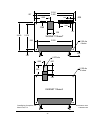
3.934
3.480
.227
1.500
1.000
.088
.590
2.650
2.370
.534
.250
.190
XM-ENET 10baseT
.342
3.250
0.100 dia
4 holes
.500
.140
0.375 dia
1.000
.500
0.100 dia
4 holes
.935
.335
XM-ENET 10base2
GreenSpring Computers, Inc.
Menlo Park, CA
IP-Ethernet Lance
Transition Module
35
36