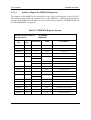
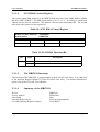
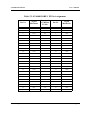
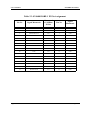
1
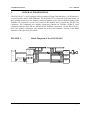
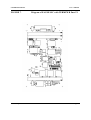
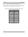
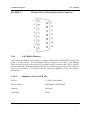
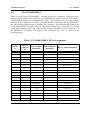
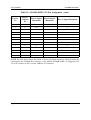
SYS68K/EAGLE-01C Reference Guide P/N 202064 Edition 6.0 October 2001 Copyright The information in this publication is subject to change without notice. Force Computers, GmbH reserves the right to make changes without notice to this, or any of its products, to improve reliability, performance, or design. Force Computers, GmbH shall not be liable for technical or editorial errors or omissions contained herein, nor for indirect, special, incidental, or consequential damages resulting from the furnishing, performance, or use of this material. This information is provided “as is” and Force Computers, GmbH expressly disclaims any and all warranties, express, implied, statutory, or otherwise, including without limitation, any express, statutory, or implied warranty of merchantability, fitness for a particular purpose, or non-infringement. This publication contains information protected by copyright. This publication shall not be reproduced, transmitted, or stored in a retrieval system, nor its contents used for any purpose, without the prior written consent of Force Computers, GmbH. Force Computers, GmbH assumes no responsibility for the use of any circuitry other than circuitry that is part of a product of Force Computers, GmbH. Force Computers, GmbH does not convey to the purchaser of the product described herein any license under the patent rights of Force Computers, GmbH nor the rights of others. Copyright 2001 by Force Computers, GmbH. All rights reserved. The Force logo is a trademark of Force Computers, GmbH. IEEE is a registered trademark of the Institute for Electrical and Electronics Engineers, Inc. PICMG, CompactPCI, and the CompactPCI logo are registered trademarks and the PICMG logo is a trademark of the PCI Industrial Computer Manufacturer’s Group. MS-DOS, Windows95, Windows98, Windows2000 and Windows NT are registered trademarks and the logos are a trademark of the Microsoft Corporation. Intel and Pentium are registered trademarks and the Intel logo is a trademark of the Intel Corporation. Other product names mentioned herein may be trademarks and/or registered trademarks of their respective companies. World Wide Web: www.forcecomputers.com 24-hour access to on-line manuals, driver updates, and application notes is provided via SMART, our SolutionsPLUS customer support program that provides current technical and services information. Headquarters The Americas Europe Asia Force Computers Inc. 5799 Fontanoso Way San Jose, CA 95138-1015 U.S.A. Force Computers GmbH Prof.-Messerschmitt-Str. 1 D-85579 Neubiberg/München Germany Force Computers Japan KK Shiba Daimon MF Building 4F 2-1-16 Shiba Daimon Minato-ku, Tokyo 105-0012 Japan Tel.: +1 (408) 369-6000 Fax: +1 (408) 371-3382 Email: [email protected] Tel.: +49 (89) 608 14-0 Fax: +49 (89) 609 77 93 Email: [email protected] Tel.: +81 (03) 3437 3948 Fax: +81 (03) 3437 3968 Email: [email protected] 202064 420 000 AA EAGLE-01C USER’S MANUAL Table of Contents Table of Contents 1. 1.1. 1.2. 1.3. 1.4. 1.5. 1.6. 1.7. GENERAL INFORMATION...................................................................1 The FLXibus................................................................................................2 The Floppy Interface ...................................................................................2 The SCSI Interface ......................................................................................3 The LAN Interface.......................................................................................4 EAGLE FLASH EPROM............................................................................4 Diagram of EAGLE-01C with Switches SW1 and SW2 ............................5 Default Settings of Switches SW1 and SW2...............................................6 2. 2.1. 2.2. 2.2.1. 2.2.1.1. 2.2.1.2. 2.2.1.3. 2.2.2. 2.2.2.1. 2.2.2.2. 2.2.2.3. 2.2.3. 2.2.3.1. 2.2.4. 2.2.4.1. 2.3. 2.3.1. 2.3.1.1. 2.3.1.2. 2.3.1.3. 2.3.1.4. 2.3.1.5. 2.3.1.6. 2.3.2. 2.3.2.1. 2.3.2.2. 2.3.2.3. 2.3.2.4. 2.3.2.5. HARDWARE DESCRIPTION ................................................................7 Address Map of the EAGLE-01C ...............................................................7 Floppy Interface...........................................................................................7 Floppy Disk Controller 37C65 ................................................................... 8 Address Map of the 37C65......................................................................... 8 The FDC Interrupt ...................................................................................... 9 Summary of the 37C65............................................................................... 9 The LCA ..................................................................................................... 9 LCA Data Transfers.................................................................................. 10 LCA DMA Control Lines......................................................................... 11 LCA DMA Control Register .................................................................... 12 Floppy Buffer Memory............................................................................. 12 Summary of the Floppy Buffer Memory .................................................. 13 The Floppy Disk Bus ................................................................................ 13 The Floppy Drive Signals on VMEbus P2 Connector ............................. 16 SCSI Interface............................................................................................17 SCSI Controller MB87034 ....................................................................... 17 Address Map of the MB87034 Registers ................................................. 18 The SCSI CPU Interface........................................................................... 19 The SCSI DMA Interface ......................................................................... 19 SCSI DMA Control Register.................................................................... 20 The MB87034 Interrupt............................................................................ 20 Summary of the MB87034 ....................................................................... 20 SCSIbus .................................................................................................... 21 SCSIbus Configuration............................................................................. 21 SCSIbus Signals ....................................................................................... 24 SCSIbus Signal Termination .................................................................... 25 SCSIbus Termination Resistor Power (TERMPWR)............................... 26 The SCSIbus Signals on VMEbus P2 Connector ..................................... 28 Force Computers Page v Table of Contents EAGLE-01C USER’S MANUAL 2.4. 2.4.1. 2.4.1.1. 2.4.1.2. 2.4.1.3. 2.4.2. 2.4.2.1. 2.4.2.2. 2.4.3. 2.4.3.1. 2.4.4. 2.4.4.1. 2.5. 2.5.1. 2.6. The LAN Interface.....................................................................................29 LAN Controller for Ethernet (LANCE) AM79C90 ................................. 30 Address Map of the LANCE Registers .................................................... 31 The LANCE Interrupt............................................................................... 32 Summary of the LANCE .......................................................................... 32 The Am7992B Serial Interface Adapter (SIA)......................................... 33 The Am7992B Transmitter....................................................................... 34 The Am7992B Receiver ........................................................................... 35 Ethernet Signals ........................................................................................ 36 Ethernet on the 15-Pin Female D-Sub Connector .................................... 38 LAN Buffer Memory................................................................................ 39 Summary of the LAN RAM ..................................................................... 39 The EAGLE FLASH EPROM ..................................................................40 Summary of the EAGLE FLASH EPROM .............................................. 40 The SYS68K/IOBP-1 ................................................................................41 3. ORDERING INFORMATION ..............................................................47 4. HISTORY OF MANUAL REVISIONS ................................................47 5. OTHER SOURCES OF INFORMATION............................................48 Page vi Force Computers EAGLE-01C USER’S MANUAL Table of Contents List of Figures Figure 1. Figure 2. Figure 3. Figure 4. Figure 5. Figure 6. Figure 7. Figure 8. Figure 9. Figure 10. Figure 11. Force Computers Block Diagram of the EAGLE-01C .................................................... 1 Diagram of EAGLE-01C with SW1 and SW2 .................................... 5 Default Setting of Dip Switch Array SW1 .......................................... 6 Default Setting of Dip Switch Array SW2 .......................................... 6 SCSI I.D. Bits .................................................................................... 22 Sample SCSI Configurations............................................................. 23 Diagram of EAGLE-01C with TERMPWR Fuse F1 ........................ 27 Manchester II Code Transmitter Encoding ....................................... 34 Decoding with the Manchester Decoder ........................................... 35 Diagram of EAGLE-01C with Fuse F2............................................. 37 Pinout of the 15-Pin Female D-Sub Connector ................................. 39 Page vii Table of Contents Page viii EAGLE-01C USER’S MANUAL Force Computers EAGLE 01C USER‘S MANUAL Table of Contents List of Tables Table 1. Table 2. Table 3. Table 4. Table 5. Table 6. Table 7. Table 8. Table 9. Table 10. Table 11. Table 12. Table 13. Table 14. Table 15. Table 16. Table 17. Table 18. Table 19. Table 20. Table 21. Table 22. Table 23. Table 24. Table 25. Table 26. Table 27. Address Map of the EAGLE-01C .............................................................. 7 Register Layout of the 37C65..................................................................... 8 Address Map for Generating TC .............................................................. 11 LCA DMA Control Register Layout ........................................................ 12 Description of LCA DMA Control Register Bits ..................................... 12 SW1 Setting for MO12/HEADLOAD ..................................................... 13 Address Map for Generating EJECT........................................................ 14 SW1 Setting for HEADLOAD/EJECT .................................................... 14 SW1 Setting for DRIVE TYPE ................................................................ 15 SW1 Setting for PRECOMPENSATION VALUE .................................. 15 SWI Setting for DISK CHANGE ENABLE ............................................ 15 Pin Assignment for Floppy Drive Signals on VMEbus P2 ...................... 16 MB87034 Register Layout ....................................................................... 18 SCSI DMA Control Register.................................................................... 20 SCSI DMA Direction Bit ......................................................................... 20 SW2 Setting for SCSI Termination .......................................................... 25 Pin Assignment for SCSIbus Signals on VMEbus P2.............................. 28 LANCE Register Layout .......................................................................... 31 Pin Assignment of the 15-Pin Female D-Sub Connector ......................... 38 SW1 Setting for FLASH EPROMs .......................................................... 40 SYS68K/IOBP-1 P1 Pin Assignment....................................................... 41 SYS68K/IOBP-1 P2 Pin Assignment....................................................... 43 SYS68K/IOBP-1 P3 Pin Assignment....................................................... 44 SYS68K/IOBP-1 P4 Pin Assignment....................................................... 45 Ordering Information................................................................................ 47 History of Manual Revisions .................................................................... 47 OTHER SOURCES OF INFORMATION............................................... 48 Force Computers Page ix Table of Contents Page x EAGLE-01C USER’S MANUAL Force Computers SYS68K/EAGLE-01C 1. User’s Manual GENERAL INFORMATION The EAGLE-01C is an I/O module which contains a Floppy Disk Interface, a SCSI Interface, a LAN Interface and FLASH EPROMs. The EAGLE-01C is connected to the base board via three module connectors. One module connector connects to the 64 user-defined signals of the VMEbus P2 Connector via the base board to the module and is called the EAGLE I/O Connector. The remaining two module connectors contain the FLXibus (FORCE Local eXpansion interface bus) and are called EAGLE FLXibus Connectors. On the EAGLE-01C, these two module connectors also contain the 8-bit Local Interface and the 8-bit DMA Interface of the gate array FGA-002. FIGURE 1. Block Diagram of the EAGLE-01C FLXibus FGA Interface SCSI DMA Interface Control CONTROLLER LANCE SIA Address WITH DMA ETHERNET CONTROLLER Data Local Interface FGA Control 16 KBYTE P2 ETHERNET SRAM BUFFER RAM VMEbus BUFFER 64 KBYTE FLOPPY FLASH CONTROLLER LCA EPROM 256 KBYTE Force Computers Page 1 User’s Manual 1.1 SYS68K/EAGLE-01C The FLXibus The FLXibus (FORCE Local eXpansion interface bus) is an interface which allows the connection between an EAGLE module and a base board. The FLXibus is a 32-bit interface with non-multiplexed data and address lines. The FLXibus is fully compatible to the 68020 bus timing. The dynamic bus sizing mechanism of the 68020 is fully supported. The bus activities use the asynchronous protocol so that all 68020 compatible devices can be connected to the FLXibus. An EAGLE module is connected with the base board via three connectors. The EAGLE FLXibus Connectors hold the signals of the FLXibus. The EAGLE I/O Connector holds the I/O signals which are routed to the VMEbus P2 of the base board. 1.2 The Floppy Interface The Floppy Interface on the EAGLE-01C is built with the 37C65 Floppy Disk Controller. A 16 Kbyte Buffer Memory and a DMA Controller allow read and write of a sector without any decrease in CPU or main (shared) RAM performance. This configuration is installed for maximum performance and real-time capability of the system. The Floppy Interface allows the control of two floppy drives. The Floppy Interface supports 3 1/2”, 5 1/4” and 8" floppy drives. Interrupts of the 37C65 are fully supported. The I/O signals of the Floppy Interface are provided on the VMEbus P2 Connector of the base board via the EAGLE I/O Connector. The floppy drives can be connected to the VMEbus P2 Connector via the backpanel SYS68K/ IOBP-1. The DMA Controller is built in an LCA (logic cell array) which is a field programmable gate array. The LCA manages the data transfer between the CPU, the 16 Kbyte Buffer Memory and the Floppy Disk Controller. (Please see “Block Diagram of the EAGLE-01C” on page 1.) The LCA manages the following accesses: • CPU to Floppy Disk Controller. • CPU to 16 Kbyte Buffer Memory. • Floppy Disk Controller to 16 Kbyte Buffer Memory via the DMA controller built in the LCA. Page 2 Force Computers SYS68K/EAGLE-01C 1.3 User’s Manual The SCSI Interface On the EAGLE-01C the MB87034 SCSI Controller is installed for direct interface to SCSI Winchester disks, optical drives, tape streamers and other SCSI compatible devices with a data transfer rate of up to 4 Mbyte/s. Interrupts of the MB87034 are fully supported. The I/O signals of the SCSI interface are provided on the VMEbus P2 Connector of the base board via the EAGLE I/O Connector. The mass memory devices can be connected to the VMEbus P2 Connector via the backpanel SYS68K/IOBP-1. The MB87034 is directly connected to the 8-bit Local Interface and the 8-bit DMA Interface of the FGA-002 via the EAGLE FLXibus connectors. The 8-bit Local Interface of the FGA-002 is used to access the registers of the MB87034. Parity is generated by the internal MB87034 parity generator when writing to the registers. The 8-bit DMA Interface is used to transfer data between the DMA channel of the MB87034 and the DMA Controller of the FGA-002. Parity is generated by an external parity generator when writing to the DMA channel of the MB87034. The DMA Controller of the FGA-002 contains a 32-byte FIFO. The DMA channel of the FGA-002 contains an additional 8 byte FIFO. This allows data transfer via the DMA Interface of the FGA-002 with a data rate of 4 Mbyte/s. In a DMA READ transfer the DMA Controller waits until the FIFO is filled with SCSI data and then requests local bus mastership to transfer the 32 bytes in 8 CPU cycles. In a DMA WRITE transfer the DMA Controller requests local bus mastership and fills its FIFO with 32 bytes from the source address in 8 CPU cycles. When the FIFO is filled the DMA Controller transfers the data to the DMA channel of the SCSI Controller. Force Computers Page 3 User’s Manual 1.4 SYS68K/EAGLE-01C The LAN Interface The LAN Interface on the EAGLE-01C is built with the Local Area Network Controller for Ethernet (LANCE) AM79C90, the Serial Interface Adapter (SIA) AM7992B and a 64 Kbyte Buffer Memory. Interrupts of the AM79C90 are fully supported. The LAN Interface is Ethernet and IEEE 802.3 10 BASE 5 Type A compatible. The I/O signals of the LAN Interface are provided on the D-Sub Connector on the front panel. The memory buffer is a shared memory allowing access from both the AM79C90 and the local CPU. The 64 Kbyte Buffer Memory stores the incoming and outgoing data packets. An incoming data packet is transferred to the Buffer Memory by the LAN Controller. The presence of data in the Buffer Memory is indicated to the CPU by an interrupt. The CPU can then read the data packet from the Buffer Memory. An outgoing data packet is transferred to the Buffer Memory by the CPU. The LAN Controller then transfers the data packet to the network and indicates the completion of the transfer by an interrupt to the CPU. The advantage of this architecture is that the CPU and the Ethernet Controller can operate in parallel which guarantees the full real-time capability in a LAN environment and the maximum performance of the system. 1.5 EAGLE FLASH EPROM On the EAGLE-01C, 256 Kbytes of FLASH EPROM are installed. The FLASH EPROM area is 8-bit wide and contains information about the EAGLE-01C for the base board. This information is read by the base board to identify the EAGLE-01C after a reset. The FLASH EPROM area also contains the low level software drivers for the I/O devices of the EAGLE-01C. FLASH EPROMs can be erased and reprogrammed electrically without removing them from the board. Therefore FLASH EPROMs ensure easy maintenance and update of software. Page 4 Force Computers SYS68K/EAGLE-01C 1.6 User’s Manual Diagram of EAGLE-01C with Switches SW1 and SW2 The following figure shows a diagram of the EAGLE-01C. The figures on the next page show the default settings of switches SW1 and SW2. FIGURE 2. Force Computers Diagram of EAGLE-01C with SW1 and SW2 Page 5 User’s Manual SYS68K/EAGLE-01C 1.7 Default Settings of Switches SW1 and SW2 FIGURE 3. Default Setting of Dip Switch Array SW1 ON OFF 01 FIGURE 4. 02 03 04 05 06 07 08 09 10 Default Setting of Dip Switch Array SW2 ON OFF 01 Page 6 02 Force Computers SYS68K/EAGLE-01C User’s Manual 2. HARDWARE DESCRIPTION 2.1 Address Map of the EAGLE-01C The following table shows the address map of the EAGLE-01C. It contains the access addresses of all I/O devices and memory devices of the EAGLE-01C. Table 1: Address Map of the EAGLE-01C Start Address FD800000 FEF00000 FEF80000 FF803400 FF803800 FF880000 2.2 End Address FD83FFFF FEF0FFFF FEF80003 FF8035FF FF8039FF FF883FFF I/O Device Type FLASH EPROMs LAN Buffer Memory LAN Controller SCSI Controller Floppy Disk Controller Floppy Buffer Memory Floppy Interface The Floppy Interface on the EAGLE-01C is built with the Floppy Disk Controller 37C65, a 16 Kbyte SRAM Buffer Memory, and an LCA (logic cell array), which is a programmable gate array. The Floppy Interface is byte-wide and is connected to the CPU on the base board via the EAGLE FLXibus Connectors. This LCA contains a data manager which manages the data transfer between the CPU, the 16 Kbyte Buffer Memory and the Floppy Disk Controller. (See “Block Diagram of the EAGLE-01C” on page 1.) The Floppy Interface allows the control of two floppy drives. The Floppy Interface supports 3 1/2", 5 1/4" and 8" floppy drives. Single, double and high density floppies are supported. The I/O signals of the Floppy Interface are provided on the VMEbus P2 Connector of the base board via the EAGLE I/O Connector. The floppy drives can be connected to the VMEbus P2 Connector via the backpanel SYS68K/ IOBP-1. (See “The SYS68K/IOBP-1” on page 41.) Force Computers Page 7 User’s Manual 2.2.1 SYS68K/EAGLE-01C Floppy Disk Controller 37C65 The Floppy Disk Controller 37C65 is an LSI device used to interface floppy drives to a CPU bus. The chip integrates the formatter/controller, data separation, write precompensation, data rate selection and clock generation. The chip also contains the drivers and receivers for the Floppy Disk bus so that no additional buffers are necessary. Features of the Floppy Disk Controller • IBM PC AT compatible format (single, double, and high density) • Data transfer in DMA or non-DMA mode • Direct floppy disk drive interface • Internal address mark detection circuitry • 128, 256, 512, 1024, 2048 or 4096 bytes sector length • Multisector and multitrack transfer capability • Automatic write precompensation 2.2.1.1 Address Map of the 37C65 The registers of the 37C65 are accessible via the 8-bit Local Interface of the FGA-002. The following table shows the register layout of the 37C65. Additional information is provided in the 37C65 Data Sheet, a copy of which can be found in “OTHER SOURCES OF INFORMATION” on page 48. Table 2: Register Layout of the 37C65 Default I/O Base Address: Default Offset: $FF800000 $00003800 Address HEX Offset HEX Mode Label Description FF803800 FF803801 FF803802 FF803803 00 01 02 03 R/W R/W R/W W STATREG DATAREG CTRLREG OPREG Master Status register Data register Control register Operation register Page 8 Force Computers SYS68K/EAGLE-01C 2.2.1.2 User’s Manual The FDC Interrupt The interrupt of the FDC is programmable in the FGA-002 Gate Array. It is connected to the Interrupt Request Channel #1 of the FGA-002 Gate Array. For detailed information please refer to the FGA-002 User’s Manual. 2.2.1.3 Summary of the 37C65 Device 37C65 Access Address $FF803800 Port Width Byte Interrupt Request Level Software programmable FGA-002 Interrupt Request Channel Local IRQ #1 2.2.2 The LCA The LCA on the EAGLE-01C manages the data transfer between the CPU via the Local I/O Interface of the FGA-002, the Buffer Memory, and the Floppy Disk Controller. (See “Block Diagram of the EAGLE-01C” on page 1.) The LCA controls the Buffer Memory and the Floppy Disk Controller. Three paths for data transfers are possible: (1) CPU <==> Floppy Disk Controller The CPU can read from or write to the Floppy Disk Controller via the LCA (non-DMA mode). (2) CPU <==> Buffer Memory The CPU can read from or write to the 16 Kbyte Buffer Memory via the LCA (non-DMA mode). (3) Floppy Disk Controller <==> Buffer Memory The Floppy Disk Controller can read from or write to the 16 Kbyte Buffer Memory via the DMA controller which is inside the LCA (DMA mode). Force Computers Page 9 User’s Manual 2.2.2.1 SYS68K/EAGLE-01C LCA Data Transfers The CPU accesses the Floppy Disk Controller via the FGA-002 for initializing, for writing the floppy commands and for reading the status information of the Floppy Disk Controller. When the Floppy Disk Controller is initialized and it has received a floppy command (e.g. read/write a sector/track command), the Floppy Disk Controller starts transferring the floppy data bytes. The Floppy Disk Controller can be initialized in DMA mode and in non-DMA mode. The data transfer of floppy data is described as follows: Non-DMA Mode In non-DMA mode floppy data is transferred by the CPU. The Floppy Disk Controller generates an interrupt to the CPU when it has received a data byte from the floppy drive or when it wants to send a data byte to the floppy drive. The CPU must then transfer the data byte to or from the Floppy Disk Controller within a certain amount of time so that no data will be lost. For each byte which has to be transferred the Floppy Disk Controller will generate an interrupt. DMA Mode In DMA mode floppy data is transferred with the help of the DMA controller inside the LCA. The Floppy Disk Controller generates a DMA request to the LCA when it has received a data byte from the floppy drive (DMA READ) or when it wants to send a data byte to the floppy drive (DMA WRITE). After each DMA request the LCA generates a DMA acknowledge to the Floppy Disk Controller. The LCA contains a DMA Control Register. One bit holds the information for the LCA about the direction of the DMA transfer (DMA READ or DMA WRITE). It has to be set to the right value before a DMA transfer is started. (See “LCA DMA Control Register” on page 12.) In a DMA READ operation the LCA transfers byte for byte of the floppy data (e.g. a sector or a track) from the Floppy Disk Controller into the Buffer Memory. When the transfer is complete the Floppy Disk Controller generates an interrupt to the CPU to indicate that the buffer memory is filled with the floppy data and that the Buffer Memory can be read by the CPU. Before a DMA WRITE operation is started the CPU has to fill the Buffer Memory with the floppy data (e.g. a sector or a track). Then the LCA transfers byte for byte of the floppy data from the Buffer Memory to the Floppy Disk Controller. When the transfer is complete the Floppy Disk Controller generates an interrupt to the CPU to indicate that the memory buffer has been read by the Floppy Disk Controller and the floppy data has been transferred. Page 10 Force Computers SYS68K/EAGLE-01C 2.2.2.2 User’s Manual LCA DMA Control Lines The LCA automatically generates the DMA control lines for the Floppy Disk Controller. A DMA control line called TC (Terminal Count) exists on the Floppy Disk Controller. TC is used to stop a data transfer between the Floppy Disk Controller and the Floppy Drive. This is done by accessing a dedicated address (read or write access). This address is shown in the table below. TC will become active during the access and inactive after the access. Additional information is provided in the FDC Data Sheet, a copy of which may be found in “OTHER SOURCES OF INFORMATION” on page 48. Table 3: Address Map for Generating TC Default I/O Base Address: Default Offset: $FF800000 $00003800 Address Hex Offset Hex Mode Label Description FF803805 05 R/W TC Terminal Count Force Computers Page 11 User’s Manual 2.2.2.3 SYS68K/EAGLE-01C LCA DMA Control Register The LCA contains a register which controls the DMA transfer between Floppy Controller and the Buffer Memory. Register bit 0 controls the direction of the DMA transfer and must be set to the right value before a DMA transfer is started. The register bit 0 can be read back. Register bit 1 indicates whether a DMA transfer is in progress or not. It can only be read and will not be affected by a write access. Table 4: LCA DMA Control Register Layout Default I/O Base Address: Default Offset: $FF800000 $00003804 Address HEX Offset HEX Mode Reset Value Label Description FF803804 04 R/W FC LCAREG DMA Control Register Table 5: Description of LCA DMA Control Register Bits Bit Value Mode 0 1 0 R/W 1 1 0 R 2.2.3 Description Buffer Memory to Floppy Disk Controller (DMA WRITE) Floppy Disk Controller to Buffer Memory (DMA READ) DMA transfer in progress DMA transfer ready Floppy Buffer Memory The Floppy Interface of the EAGLE-01C holds a 16 Kbyte Buffer Memory. The Buffer Memory can be accessed by the CPU and by the Floppy Disk Controller via the LCA. (See the chapter “LCA Data Transfers” on page 10.) The Floppy Buffer Memory is accessed by the CPU via the 8-bit Local I/O Interface of the FGA-002 in the address range $FF880000 to $FF883FFF. When the Floppy Buffer Memory is accessed by the Floppy Disk Controller, the LCA generates the address for the Buffer Memory. The address is set to zero at the beginning of a DMA transfer and is counted upwards by the LCA during the DMA transfer. Page 12 Force Computers SYS68K/EAGLE-01C 2.2.3.1 User’s Manual Summary of the Floppy Buffer Memory Device 32K * 8 SRAM Addressable Space 16 Kbytes Access Address $FF880000 to $FF883FFF Port Width Byte 2.2.4 The Floppy Disk Bus The floppy disk bus is an SA450 type drive interface. The floppy drive signals are provided directly from the Floppy Disk Controller with no additional buffers. Some of the floppy drive signals can be changed via switch 1 to switch 8 of the dip switch array SW1. The switches must be changed for the different types of floppy drives which are used. Switch 9 is used for the LCA configuration mode and must not be changed by the user. Switch 10 is used for the write protection of the FLASH EPROMs and is described in the chapter “The EAGLE FLASH EPROM” on page 40. The default setting of the dip switch array SW1 is shown in “Default Setting of Dip Switch Array SW1” on page 6 and the location of SW1 is shown in the “Diagram of EAGLE-01C with SW1 and SW2” on page 5. The following floppy disk signals can be changed via the dip switch array SW1: MO12/HEADLOAD The motor on signals MO1/DS3 and MO2/DS4 of the Floppy Disk Controller are open collector lines. They are tied together and have the signal name MO12. Via switch 1 and switch 2 either MO12 or HEADLOAD can be connected to the MOTOR ON signal of the floppy drive. So both signals can be used to start the motor of the floppy drive. CAUTION: The switches must not be both opened or both closed at the same time. Table 6: SW1 Setting for MO12/HEADLOAD Active Signal SW1-1 SW1-2 Default Setting MO12 OFF ON * HEADLOAD ON OFF Force Computers Page 13 User’s Manual SYS68K/EAGLE-01C HEADLOAD/EJECT There are special 3 1/2" drives which need an eject pulse to eject the floppy out of the drive. The eject signal must be connected to the pin which normally holds the HEADLOAD signal. Via switch SW1-3 and switch SW1-4 either HEADLOAD or EJECT can be connected to the floppy drive. The EJECT signal can be generated by accessing (read or write) a dedicated address. EJECT is active during the read or write cycle to this address and automatically becomes inactive after two microseconds. Table 7: Address Map for Generating EJECT Default I/O Base Address: Default Offset: $FF800000 $00003806 Address HEX Offset HEX Mode Label Description FF803806 06 R/W EJECT Ejection of Floppy disk CAUTION: The switches must not be both opened or both closed at the same time. Table 8: SW1 Setting for HEADLOAD/EJECT Page 14 Active Signal SW1-3 SW1-4 Default Setting HEADLOAD OFF ON * EJECT ON OFF Force Computers SYS68K/EAGLE-01C User’s Manual DRIVE TYPE The DRIVE TYPE (DRV) signal is used to indicate to the Floppy Disk Controller whether a floppy drive with a two-spindle motor or a one-spindle motor is used. CAUTION: Take care that a switch setting with one switch opened and the other one closed is never used. Table 9: SW1 Setting for DRIVE TYPE Drive Type SW1-5 SW1-6 One-Spindle Motor OFF OFF Two-Spindle Motor ON ON Default Setting * PRECOMPENSATION VALUE The PRECOMPENSATION VALUE (PCVAL) signal is used to select the write precompensation time of the Floppy Disk Controller. The time is selected via SW1-7. Table 10: SW1 Setting for PRECOMPENSATION VALUE Precompensation Time SW1-7 Default Setting 125 ns OFF * 187 ns ON DISK CHANGE ENABLE The DISK CHANGE ENABLE (DCHGEN) signal is used to enable the DCHG input status at pin 40 of the Floppy Disk Controller. DCHG is the door lock signal of the floppy drive and indicates whether the door of the floppy drive is open or not. Table 11: SWI Setting for DISK CHANGE ENABLE DCHG Signal SW1-8 Enabled ON Disabled OFF Force Computers Default Setting * Page 15 User’s Manual 2.2.4.1 SYS68K/EAGLE-01C The Floppy Drive Signals on VMEbus P2 Connector The floppy drive signals are available on the EAGLE I/O Connector which is connected to row C of the VMEbus P2 Connector. The pin assignment for the floppy disk signals is shown in the table below. The floppy drives can be connected to the VMEbus P2 Connector via the backpanel SYS68K/IOBP-1. (Please see also the chapter “The SYS68K/IOBP-1” on page 41.) Table 12: Pin Assignment for Floppy Drive Signals on VMEbus P2 Page 16 Pin Number Signal Mnemonic C1 C2 C3 C4 C5 C6 C7 C8 C9 C!0 C11 C12 C13 C14 C15 C16 C17 RWC/RPM HEADLOAD/EJECT DRIVE SELECT 2 INDEX DRIVE SELECT 1 DRIVE SELECT 2 DRIVE SELECT 1 MOTOR ON/HEADLOAD DIRECTION IN STEP WRITE DATA WRITE GATE TRACK 000 WRITE PROTECT READ DATA HEAD SELECT DISK CHANGE Force Computers SYS68K/EAGLE-01C 2.3 User’s Manual SCSI Interface The SCSI Interface on the EAGLE-01C is built with the SCSI Controller MB87034. The SCSI Interface is installed for direct interface to SCSI Winchester disks, optical drives, tape streamers and other SCSI compatible devices with a data transfer rate of up to 5 Mbyte/s. The I/O signals of the SCSI interface are provided on the VMEbus P2 Connector of the base board via the EAGLE I/O Connector. The SCSI devices can be connected to the VMEbus P2 Connector via the backpanel SYS68K/IOBP-1. (Please see the chapter “The SYS68K/IOBP1” on page 41.) 2.3.1 SCSI Controller MB87034 The SCSI Controller MB87034 is a CMOS LSI chip designed to control a SCSI Interface. The MB87034 can serve as either an INITIATOR or TARGET for the SCSIbus. The Controller contains an 8 byte FIFO data buffer register and a 28-bit transfer byte counter. The Controller has two independent 8-bit buses for the DMA transfer and non-DMA transfer. Features of the MB87034 SCSI Controller • Full support for SCSI control • Serves as either initiator or target device • Eight byte data buffer register incorporated • Transfer byte counter (28-bit) • Independent control and data transfer bus • Asynchronous data transfer speed of 2 Mbytes/sec • Synchronous data transfer speed of up to 4 Mbytes/sec Force Computers Page 17 User’s Manual 2.3.1.1 SYS68K/EAGLE-01C Address Map of the MB87034 Registers The registers of the MB87034 are accessible via the 8-bit Local Interface of the FGA-002. The following table shows the register layout of the MB87034. Additional information is provided in the MB87034 Data Sheet, a copy of which may be found in “OTHER SOURCES OF INFORMATION” on page 48 . Table 13: MB87034 Register Layout Default I/O Base Address: Default Offset: $FF800000 $00003400 Address Hex Offset Hex Read/Write Label Description FF803400 00 R/W BDID BUS DEVICE ID FF803401 01 R/W SCTL SPC CONTROL FF803402 02 R/W SCMD COMMAND FF803403 03 R/W TMOD TRANSFER MODE FF803404 04 R INTS INTERRUPT SENSE W FF803405 05 RESET INTERRUPT R PSNS PHASE SENSE W SDGC SPC DIAGNOSTIC CONTROL FF803406 06 R SSTS SPC STATUS FF803407 07 R SERR SPC ERROR STATUS FF803408 08 R/W PCTL PHASE CONTROL FF803409 09 R MBC MODIFIED BYTE COUNTER W Page 18 EXTENDED TRANSFER COUNT FF80340A 0A R DREG DATA REGISTER FF80340B 0B R TEMP TEMPORARY REGISTER FF80340C 0C R TCH TRANSFER COUNT HIGH FF80340D 0D R TCM TRANSFER COUNT MIDDLE FF80340E 0E R TCL TRANSFER COUNT LOW FF80340F 0F R EXBF EXTERNAL BUFFER Force Computers SYS68K/EAGLE-01C 2.3.1.2 User’s Manual The SCSI CPU Interface The 8-bit Local Interface of the FGA-002 is used to access the registers of the MB87034. Parity is generated by the internal MB87034 parity generator when writing to the registers 2.3.1.3 The SCSI DMA Interface The 8-bit DMA channel of the SCSI Controller is directly connected to the installed DMA Controller of the FGA-002 allowing data transfers with a maximum speed of 4 Mbyte/s. Parity is generated by an external parity generator when writing to the DMA channel of the MB87034. The DMA Controller of the FGA-002 contains a 32-byte FIFO. The DMA channel of the FGA-002 contains an additional 8 byte FIFO. This allows data transfer via the DMA Interface of the FGA-002 with a data rate of 4 Mbyte/s. In a DMA READ transfer the DMA Controller waits until the FIFO is filled with SCSI data and then requests CPU bus mastership to transfer the 32 bytes in 8 CPU cycles. In a DMA WRITE transfer the DMA Controller requests CPU bus mastership and fills its FIFO with 32 bytes from the source address in 8 CPU cycles. When the FIFO is filled the DMA Controller transfers the data to the DMA channel of the SCSI Controller. Force Computers Page 19 User’s Manual 2.3.1.4 SYS68K/EAGLE-01C SCSI DMA Control Register The control signal HIN indicates to the MB87034 the direction of the DMA transfer (DMA READ or DMA WRITE). The HIN signal can be set to "0" or "1" by writing to a dedicated address and can also be read back. The address is shown in the following table. The second table shows the function of the register bit. Table 14: SCSI DMA Control Register Default I/O Base Address: $FF800000 Default Offset: $00002C00 Address HEX Offset HEX Mode Description FF802C00 00 R/W SCSI DMA Control Register Table 15: SCSI DMA Direction Bit 2.3.1.5 Bit Value Description 0 1 Data from SCSI Controller to FGA-002 (DMA READ) 0 Data from FGA-002 to SCSI Controller (DMA WRITE) The MB87034 Interrupt The interrupt of the MB87034 is programmable in the FGA-002 Gate Array. It is connected to the Interrupt Request Channel #7 of the FGA-002 Gate Array. For detailed information, please refer to the FGA-002 User’s Manual. 2.3.1.6 Summary of the MB87034 Device Access Address Port Width Interrupt Request Level FGA-002 Interrupt Request Channel Page 20 MB87034 $FF803400 Byte Software programmable Local IRQ #7 Force Computers SYS68K/EAGLE-01C 2.3.2 SCSIbus 2.3.2.1 SCSIbus Configuration User’s Manual Communication on the SCSIbus is only allowed between two SCSI devices at any given time. There is a maximum of eight SCSI devices. Each SCSI device has a SCSI I.D. bit assigned as shown in “SCSI I.D. Bits” on page 22. When two SCSI devices communicate on the SCSIbus, one acts as an initiator and the other acts as a target. A SCSI device usually has a fixed role as an initiator or target, but some devices may be able to assume either role. An initiator may address up to seven peripheral devices that are connected to a target. An option allows the addressing of up to 2.048 peripheral devices per target using extended messages. Three sample system configurations are shown in “Sample SCSI Configurations” on page 23. Force Computers Page 21 User’s Manual SYS68K/EAGLE-01C FIGURE 5. DB(7) SCSI I.D. Bits DB(6) DB(5) DB(4) DB(3) DB(2) DB(1) DB(0) DATA BUS SCSI I.D. = 0 SCSI I.D. = 1 SCSI I.D. = 2 SCSI I.D. = 3 SCSI I.D. = 4 SCSI I.D. = 5 SCSI I.D. = 6 SCSI I.D. = 7 Up to eight devices can be supported on the SCSIbus. They can be any combination of initiators and targets. Certain SCSIbus functions are assigned to the target. The initiator may arbitrate for the SCSIbus and select a particular target. The target may request the transfer of COMMAND, DATA, STATUS, or other information and reselect an initiator for the purpose of continuing an operation. Information transfers on the data bus are asynchronous and follow a defined REQ/ACK handshake protocol. One byte of information may be transferred with each handshake. An option is defined for synchronous data transfer. Page 22 Force Computers SYS68K/EAGLE-01C User’s Manual HOST COMPUTER Sample SCSI Configurations ADAPTER FIGURE 6. Controller SCSI BUS HOST COMPUTER ADAPTER SINGLE INITIATOR, SINGLE TARGET Controller SCSI BUS HOST HOST COMPUTER Controller SCSI BUS ADAPTER COMPUTER ADAPTER SINGLE INITIATOR, MULTIPLE TARGET Controller Controller Peripheral devices such as magnetic and optical disks, printers, magnetic tapes Controller HOST COMPUTER ADAPTER Controller Controller MULTIPLE INITIATOR, MULTIPLE TARGET Force Computers Page 23 User’s Manual 2.3.2.2 SYS68K/EAGLE-01C SCSIbus Signals All SCSIbus signals are available on the EAGLE I/O Connector which is routed to the VMEbus P2 Connector. There are a total of 18 signals. Nine are used for control, and nine are used for data (data signals include the parity signal option). These signals are described as follows: ACK (ACKNOWLEDGE) A signal driven by an initiator to indicate an acknowledgment for a REQ/ ACK data transfer handshake. ATN (ATTENTION) A signal driven by an initiator to indicate the ATTENTION condition. BSY (BUSY) An "OR-tied" signal that indicates that the bus is being used. C/D (CONTROL/DATA) A signal driven by a target that indicates whether CONTROL or DATA information is on the data bus. True indicates CONTROL. DB(7-0,P) (DATA BUS) Eight data bit signals, plus a parity bit signal which together form a data bus. DB(7) is the most significant bit, and has the highest priority during the ARBITRATION phase. Bit number, significance, and priority decrease downward to DB(0). A data bit is defined as one when the signal value is true, and is defined as zero when the signal value is false. I/O (INPUT/OUTPUT) A signal driven by a target that controls the direction of data movement on the data bus with respect to an initiator. True indicates input to the initiator. This signal is also used to distinguish between SELECTION and RESELECTION phases. MSG (MESSAGE) A signal driven by a target during the MESSAGE phase. Page 24 Force Computers SYS68K/EAGLE-01C User’s Manual REQ (REQUEST) A signal driven by a target to indicate a request for a REQ/ACK data transfer handshake. RST (RESET) An "OR-tied" signal that indicates the RESET condition. SEL (SELECT) A signal used by an initiator to select a target or by a target to reselect an initiator. Data parity DB(P) is odd. The use of parity is a system option (i.e., a system configured so that all SCSI devices on a bus generate parity and have parity detection enabled, or all SCSI devices have parity detection disabled or not implemented). Parity is not valid during the ARBITRATION phase. 2.3.2.3 SCSIbus Signal Termination Each SCSIbus signal is terminated at the physical start and the physical end of the SCSIbus. Therefore, an actively terminating device is installed on the EAGLE-01C which can be enabled or disabled via dip switch SW2. For the position of SW2 on the EAGLE-01, please see “Diagram of EAGLE-01C with SW1 and SW2” on page 5. The table below outlines the switch settings for SCSI termination. Table 16: SW2 Setting for SCSI Termination SCSI Termination SW2-1 Default Setting Enabled ON * Disabled OFF Force Computers Page 25 User’s Manual 2.3.2.4 SYS68K/EAGLE-01C SCSIbus Termination Resistor Power (TERMPWR) Any SCSI device must be able to provide the power supply (TERMPWR) for the SCSI termination resistors of the SCSIbus to fulfill the SCSI Specification. On the EAGLE-01C TERMPWR is provided on the SCSIbus via a protection diode to avoid backflow of the current into the EAGLE-01C. In addition, TERMPWR is protected by a 1 Amp fuse, which is socketed and can therefore be easily exchanged. The socket for the 1 Amp fuse F1 is located on the bottom side of the EAGLE-01C. The EAGLE-01C has to be removed from the base board when exchanging the fuse F1. The figure on the next page shows the location of the fuse F1 on the EAGLE-01C. Page 26 Force Computers SYS68K/EAGLE-01C FIGURE 7. Force Computers User’s Manual Diagram of EAGLE-01C with TERMPWR Fuse F1 Page 27 User’s Manual 2.3.2.5 SYS68K/EAGLE-01C The SCSIbus Signals on VMEbus P2 Connector The SCSIbus signals are available on the EAGLE I/O Connector, which is routed to the VMEbus P2 Connector. The pin assignment for SCSI devices is shown below. The SCSI devices can be connected to the VMEbus P2 Connector via the backpanel SYS68K/IOBP-1. (Please see the chapter “The SYS68K/IOBP-1” on page 41.) Table 17: Pin Assignment for SCSIbus Signals on VMEbus P2 Page 28 Pin Number Signal Mnemonic A01 DB0 A02 DB1 A03 DB2 A04 DB3 A05 DB4 A06 DB5 A07 DB6 A08 DB7 A09 DBP A13 TERMPWR A16 ATN A18 BSY A19 ACK A20 RST A21 MSG A22 SEL A23 C/D A24 REQ A25 I/O Force Computers SYS68K/EAGLE-01C 2.4 User’s Manual The LAN Interface The LAN Interface on the EAGLE-01C is built with the Local Area Network Controller for Ethernet (LANCE) AM79C90, the Serial Interface Adapter (SIA) AM7992B and a 64 Kbyte Buffer Memory. Interrupts of the AM79C90 are fully supported. The LAN Interface is Ethernet and IEEE 802.3 10 BASE 5 Type A compatible. The I/O signals of the LAN Interface are provided on the D-Sub Connector on the front panel. Features of the LAN Interface • Compatibility to IEEE 802.3 10 BASE 5 Type A and Ethernet • Data rate of 10 Mbit per second • DMA capability • Interrupt generation • 64 Kbyte SRAM Buffer Memory The memory buffer is a shared memory allowing access from both the AM79C90 and the local CPU. The 64 Kbyte buffer memory stores the incoming and outgoing data packets. An incoming data packet is transferred to the Buffer Memory by the LAN Controller. The presence of data in the Buffer Memory is indicated to the CPU by an interrupt. The CPU can then read the data packet from the Buffer Memory. An outgoing data packet is transferred to the Buffer Memory by the CPU. The LAN Controller then transfers the data packet to the network and indicates the completion of the transfer by an interrupt to the CPU. The advantage of this architecture is that the CPU and the Ethernet Controller can operate in parallel which guarantees the full real-time capability in a LAN environment and the maximum performance of the system. Force Computers Page 29 User’s Manual 2.4.1 SYS68K/EAGLE-01C LAN Controller for Ethernet (LANCE) AM79C90 The LANCE is a 68-pin VLSI device which provides many functions for the connection of a microprocessor to the Ethernet. Features of the LAN Controller • Compatible with Ethernet and IEEE 802.3 10 BASE 5 Type A • On-chip DMA and buffer management • 48 byte transmit FIFO and 64 byte receive FIFO • 24-bit wide linear addressing • Network and packed error reporting • Back-to-back packet reception with as little as 0.5 µs interframe spacing • Diagnostic routines • Low power consumption In the transmitting mode the LANCE transfers data from the Buffer Memory to an internal FIFO called SILO. The serial output of the SILO is connected with the AM7992 SIA, where the data is sent to the Ethernet cable. In the receiving mode the SIA transfers the received data from the Ethernet cable to the serial SILO input and the LANCE transfers the data to the Buffer Memory. After reset the Control Status Registers CSR0 and CSR3 are cleared, the LANCE is stopped and can be initialized. During initialization the CPU must be bus master of the LAN bus. To start the LANCE operation the STRT bit in the CSR0 must be set. For detailed information, please refer to the AM79C90 LANCE Data Sheet found in “OTHER SOURCES OF INFORMATION” on page 48. Page 30 Force Computers SYS68K/EAGLE-01C 2.4.1.1 User’s Manual Address Map of the LANCE Registers The LANCE contains one Register Address Pointer (RAP) and four status control registers (CSR0, CSR1, CSR2, CSR3). To read or write to CSR1, CSR2, and CSR3 the LANCE must be stopped by setting the stop bit in CSR0. Therefore, CSR0 and RAP can be accessed at anytime the LANCE is in the slave mode. To read or write to a CSR the number of the CSR must be written to the RAP first. Table 18: LANCE Register Layout I/O Address: Default Offset: $FEF8 0000 $0000 0000 Address HEX Offset HEX Reset Value Label Description FEF80002 02 0000 RAP Register Address Pointer FEF80000 00 0004 CSR0 Control and Status Register 0 FEF80000 00 N/A CSR1 Control and Status Register 1 FEF80000 00 N/A CSR2 Control and Status Register 2 FEF80000 00 N/A CSR3 Control and Status Register 3 N/A = NOT APPLICABLE OR NOT EFFECTED Force Computers Page 31 User’s Manual 2.4.1.2 SYS68K/EAGLE-01C The LANCE Interrupt The interrupt of the LANCE is programmable in the FGA-002 Gate Array. It is connected to the Interrupt Request Channel #6 of the FGA-002 Gate Array. For detailed information, please refer to the FGA-002 User’s Manual. 2.4.1.3 Summary of the LANCE Device AM79C90 Access Address $FEF80000 Access Mode Word Only Interrupt Request Level Programmable FGA-002 Interrupt Request Channel Local IRQ #6 Page 32 Force Computers SYS68K/EAGLE-01C 2.4.2 User’s Manual The Am7992B Serial Interface Adapter (SIA) The Am7992B Serial Interface Adapter (SIA) is a Manchester Encoder/Decoder compatible with IEEE-802.3 10 BASE 5 TYPE A, Cheapernet, and Ethernet specifications. Features of the Am 7992B SIA • Compatible with Ethernet/Cheapernet/IEEE-802.3 10 BASE 5 TYPE A specifications • Crystal controlled Manchester Encoder • Manchester Decoder acquired clock and data within four bit times with an accuracy of +/-3 ns • Guaranteed carrier and collision detection squelch threshold limits • • • -Carrier/collision detected for inputs greater than -275 mV -No carrier/collision for inputs less than -175 mV Input signal conditioning reject transient noise • • -Transients <10 ns for collision detector inputs -Transients <20 ns for carrier detector inputs • Receiver decodes Manchester data with worst case +/-19 ns of clock jitter (at 10 MHz) • TTL compatible host interface • Transmit accuracy +/-0.01% (without adjustments) Force Computers Page 33 User’s Manual 2.4.2.1 SYS68K/EAGLE-01C The Am7992B Transmitter The transmitter encodes data coming from the LANCE into a Manchester II Code (see below). The output signal is sent to a buffer on the CPU board. An oscillator provides the 20 MHz clock signal for the LANCE. For further details, please refer to the Am7992B Data Sheet found in “OTHER SOURCES OF INFORMATION” on page 48. FIGURE 8. Manchester II Code Transmitter Encoding TX MANCHESTER TRANSMIT +/- ENCODER TENA TCLK OSC Page 34 Force Computers SYS68K/EAGLE-01C 2.4.2.2 User’s Manual The Am7992B Receiver The receiver signals the LANCE that there is a message to receive. It decodes the Manchester encoded data stream and sends the data to the LANCE (see next figure). For further information, please refer to the Am7992B Data Sheet in “OTHER SOURCES OF INFORMATION” on page 48. FIGURE 9. Decoding with the Manchester Decoder RX RCLK DATA RECEIVER CARRIER DETECT NOISE REJECT FILTER RECEIVE +/- MANCHESTER DECODER RENA Force Computers Page 35 User’s Manual 2.4.3 SYS68K/EAGLE-01C Ethernet Signals The I/O signals of the LAN Interface are provided on the 15-pin female D-Sub Connector on the front panel. On the D-Sub Connector the following Ethernet signals are available: Transmit+ / Transmit- (differential line output) This line pair is intended to operate into terminated transmission lines. Receive+ / Receive- (differential line input) This pair of internally biased line receivers consists of a carrier detect receiver and a data recovery receiver. Collision+ / Collision- (differential line input) This pair of internally biased line receivers has offset threshold and noise filtering. In addition +12 Volts/GND is available on the D-Sub Connector. The +12 Volts are protected by the 1 Amp fuse F2 to fulfill the IEEE Specification for LANs. Fuse F2 is socketed and can therefore easily be exchanged. The socket holding the fuse F2 is located on the bottom side of the EAGLE-01C. The EAGLE-0C1 does not have to be removed from the base board when exchanging the fuse F2. The fuse F2 can be short-circuited by 0-Ohm resister R46. By default, resister R46 is not assembled on the EAGLE-01C. For the location of fuse F2 on the board, please see the “Diagram of EAGLE-01C with Fuse F2” on page 37. Page 36 Force Computers SYS68K/EAGLE-01C FIGURE 10. Force Computers User’s Manual Diagram of EAGLE-01C with Fuse F2 Page 37 User’s Manual 2.4.3.1 SYS68K/EAGLE-01C Ethernet on the 15-Pin Female D-Sub Connector The Ethernet signals are available on the 15-pin female D-Sub Connector on the front panel. The pinout of the D-Sub Connector is shown in “Pinout of the 15-Pin Female D-Sub Connector” on page 39 and the pin assignment is shown in the next table. Table 19: Pin Assignment of the 15-Pin Female D-Sub Connector Page 38 Pin Number Signal Mnemonic 1 GND 2 Collision+ 3 Transmit+ 4 GND 5 Receive+ 6 GND 7 N.C. 8 GND 9 Collision- 10 Transmit- 11 N.C. 12 Receive- 13 +12V 14 GND 15 N.C. Force Computers SYS68K/EAGLE-01C FIGURE 11. User’s Manual Pinout of the 15-Pin Female D-Sub Connector 1 9 2 10 3 11 4 12 5 13 6 14 7 15 8 2.4.4 LAN Buffer Memory The LAN Buffer Memory is accessible via address $FEF00000 to $FEF0FFFF and the port width is 16 bits (word). The LAN Buffer Memory consists of two 32K * 8-bit SRAMs. These devices can be accessed by the CPU and the LANCE as long as the CPU or LANCE has bus mastership. With this dedicated memory, it is not necessary to stop the CPU while the LANCE is bus master. This assures that the real-time capability of the CPU board is guaranteed. 2.4.4.1 Summary of the LAN RAM Devices 2 * 32K * 8-bit SRAM Access Address $FEF00000 to $FEF0FFFF Capacity 64 Kbytes Port Width Word Force Computers Page 39 User’s Manual 2.5 SYS68K/EAGLE-01C The EAGLE FLASH EPROM The EAGLE-01C holds 256 Kbytes FLASH EPROM. Two 128 Kbyte FLASH EPROM devices are installed on the EAGLE-01C. The address range for the FLASH EPROMs reaches from $FD800000 to $FD83FFFF. Two 128 Kbyte devices are installed by default. For programming the FLASH EPROMs a special programming algorithm is needed. For detailed information about programming the FLASH EPROMs, see “OTHER SOURCES OF INFORMATION” on page 48. The FLASH EPROMs can be write protected by the opening of switch 10 of the dip switch array SW1. When the FLASH EPROMs must be programmed the switch 10 of the dip switch array SW1 has to be closed. The location diagram of the dip switch array SW1 is shown in “Diagram of EAGLE-01C with SW1 and SW2” on page 5. Table 20: SW1 Setting for FLASH EPROMs Write protection of FLASH EPROMs SW1-10 YES OFF NO ON 2.5.1 Default Setting * Summary of the EAGLE FLASH EPROM Devices 2 * 128K * 8 Access Address $FD800000 to $FD83FFFF Capacity 256 Kbytes Port Width Byte Page 40 Force Computers SYS68K/EAGLE-01C 2.6 User’s Manual The SYS68K/IOBP-1 There is a back-panel SYS68K/IOBP-1 available from Force Computers. This board can be plugged into the VMEbus P2 Connector of a VMEbus board which carries the EAGLE-01C. The backpanel contains the connectors (P1)...(P4). The connector (P1) is plugged on the backside of the VMEbus P2 Connector. Note that the pins of connector (P1) are numbered in the other direction than the pins of VMEbus P2 Connector. The backpanel also contains the 50-pin male SCSIbus Connector (P2), the 34-pin male Floppy Drive Connector (P3), and the 64-pin male connector (P4). The connector (P4) contains all signals of row A and row C of the VMEbus P2 Connector. The pinout of the connectors (P1)...(P4) is shown in the following tables. Table 21: SYS68K/IOBP-1 P1 Pin Assignment Pin No. P1 Pin No. VMEbus P2 Row A Signal Mnemonic Row B Signal Mnemonic Row C Signal Mnemonic 32 1 DB 0 --- RWC/RPM 31 2 DB 1 GND HEADLOAD/EJECT 30 3 DB 2 --- DRIVE SELECT 2 29 4 DB 3 --- INDEX 28 5 DB 4 --- DRIVE SELECT 1 27 6 DB 5 --- DRIVE SELECT 2 26 7 DB 6 --- DRIVE SELECT 1 25 8 DB 7 --- MOTOR ON/HEADLOAD 24 9 DB P --- DIRECTION IN 23 10 GND --- STEP 22 11 GND --- WRITE DATA 21 12 GND GND WRITE GATE 20 13 TERMPWR --- TRACK 000 19 14 GND --- WRITE PROTECT 18 15 GND --- READ DATA 17 16 ATN --- HEAD SELECT 16 17 GND --- DISK CHANGE 15 18 BSY --- N.C. 14 19 ACK --- GND Force Computers Page 41 User’s Manual SYS68K/EAGLE-01C Table 21: SYS68K/IOBP-1 P1 Pin Assignment (cont.) Pin No. P1 Pin No. VMEbus P2 Row A Signal Mnemonic Row B Signal Mnemonic Row C Signal Mnemonic 13 20 RST --- GND 12 21 MSG --- N.C. 11 22 SEL GND GND 10 23 C/D --- GND 9 24 REQ --- N.C. 8 25 I/O --- N.C. 7 26 N.C. --- N.C. 6 27 GND --- N.C. 5 28 N.C. --- N.C. 4 29 N.C. --- N.C. 3 30 N.C. --- N.C. 2 31 N.C. GND N.C. 1 32 N.C. --- N.C. NOTE:The table above shows the pinout of the 96-pin female connector which performs the connection to the VMEbus P2 Connector. If the module SYS68K/IOBP-1 is plugged in, Pin 32a of P1 connects to Pin 1a of the VMEbus P2 Connector. Page 42 Force Computers SYS68K/EAGLE-01C User’s Manual Table 22: SYS68K/IOBP-1 P2 Pin Assignment Pin No. Signal Mnemonic Connected to VMEbus P2 Pin Pin No. Signal Mnemonic 2 DB 0 A01 1 GND 4 DB 1 A02 3 GND 6 DB 2 A03 5 GND 8 DB 3 A04 7 GND 10 DB 4 A05 9 GND 12 DB 5 A06 11 GND 14 DB 6 A07 13 GND 16 DB 7 A08 15 GND 18 DB P A09 17 GND 20 GND --- 19 GND 22 GND --- 21 GND 24 GND --- 23 GND 26 TERMPWR A13 25 N.C. 28 GND --- 27 GND 30 GND --- 29 GND 32 ATN A16 31 GND 34 GND --- 33 GND 36 BSY A18 35 GND 38 ACK A19 37 GND 40 RST A20 39 GND 42 MSG A21 41 GND 44 SEL A22 43 GND 46 C/D A23 45 GND 48 REQ A24 47 GND 50 I/O A25 49 GND Force Computers Page 43 User’s Manual SYS68K/EAGLE-01C Table 23: SYS68K/IOBP-1 P3 Pin Assignment Page 44 Pin No. Signal Mnemonic Connected to VMEbus P2 Pin 2 RWC/RPM C01 1 GND 4 HEADLOAD/EJECT C02 3 GND 6 DRIVE SELECT 2 C03 5 GND 8 INDEX C04 7 GND 10 DRIVE SELECT 1 C05 9 GND 12 DRIVE SELECT 2 C06 11 GND 14 DRIVE SELECT 1 C07 13 GND 16 MOTOR ON/HEADLOAD C08 15 GND 18 DIRECTION IN C09 17 GND 20 STEP C10 19 GND 22 WRITE DATA C11 21 GND 24 WRITE GATE C12 23 GND 26 TRACK 000 C13 25 GND 28 WRITE PROTECT C14 27 GND 30 READ DATA C15 29 GND 32 HEAD SELECT C16 31 GND 34 DISK CHANGE C17 33 GND Pin No. Signal Mnemonic Force Computers SYS68K/EAGLE-01C User’s Manual Table 24: SYS68K/IOBP-1 P4 Pin Assignment Pin No. Row a Signal Mnemonic Row c Signal Mnemonic 1 DB 0 RWC/RPM 2 DB 1 HEADLOAD/EJECT 3 DB 2 DRIVE SELECT 2 4 DB 3 INDEX 5 DB 4 DRIVE SELECT 1 6 DB 5 DRIVE SELECT 2 7 DB 6 DRIVE SELECT 1 8 DB 7 MOTOR ON/HEADLOAD 9 DB P DIRECTION IN 10 GND STEP 11 GND WRITE DATA 12 GND WRITE GATE 13 TERMPWR TRACK 000 14 GND WRITE PROTECT 15 GND READ DATA 16 ATN HEAD SELECT 17 GND DISK CHANGE 18 BSY N.C. 19 ACK GND 20 RST GND 21 MSG N.C. 22 SEL GND 23 C/D GND 24 REQ N.C. 25 I/O N.C. 26 N.C. N.C. 27 GND RESERVED 28 N.C. RESERVED 29 RESERVED RESERVED 30 RESERVED RESERVED Force Computers Page 45 User’s Manual SYS68K/EAGLE-01C Table 24: SYS68K/IOBP-1 P4 Pin Assignment (cont.) Page 46 Pin No. Row a Signal Mnemonic Row c Signal Mnemonic 31 RESERVED RESERVED 32 RESERVED RESERVED Force Computers SYS68K/EAGLE-01C 3. User’s Manual ORDERING INFORMATION Table 25: Ordering Information Name of Product SYS68K/EAGLE-01C SYS68K/EAGLE-01C/UM 4. Description EAGLE Module for the CPU Board User’s Manual for the EAGLE-01C HISTORY OF MANUAL REVISIONS Table 26: History of Manual Revisions Edition No. Description Date of Last Change 0 First Print FEB/04/1991 1 Default Switch Setting in Figure 2-2 was changed AUG/16/1991 2 Default Jumper Settings in Tables 101, 2-10, 2-11 and 2-21 were changed. Default Switch Setting in Figure 1-4 was changed. JUNE/16/1992 3 Manual updated for PCB Revision 2.0 of the EAGLE-01C board. JUNE/01/1994 4 The SCSI Protocol Controller MB87033B has been replaced by the MB87034PF. MAR/14/1996 5 Editorial Changes DEC/03/1996 6 Removed data sheets and circuit schematics, editorial changes October 2001 Force Computers Page 47 User’s Manual 5. SYS68K/EAGLE-01C OTHER SOURCES OF INFORMATION For further information on components refer to the information listed in the table below. Table 27: OTHER SOURCES OF INFORMATION Company Advanced Micro Devices www. amd.com Document LAN Controller AM79C90 FLASH EPROM 28F010 FUJITSU fujitsu.com SCSI Controller - MB87034 Standard Microsystems Corporation smsc.com Floppy disk subsystem controller - FDCf37C65C Page 48 Force Computers Product Error Report Product: Serial No.: Date Of Purchase: Originator: Company: Point Of Contact: Tel.: Ext.: Address: Present Date: Affected Product: Affected Documentation: ❏ Hardware ❏ Software ❏ Systems ❏ Hardware ❏ Software ❏ Systems Error Description: This Area to Be Completed by Force Computers: Date: PR#: Responsible Dept.: ❏ Marketing ❏ Production Engineering ➠ ❏ Board ❏ Systems ☞ Send this report to the nearest Force Computers headquarter listed on the address page.