1
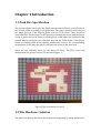
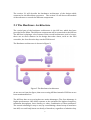
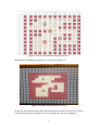
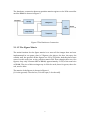
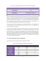
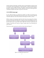
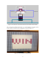
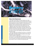
LTH Final Report Embedded Systems Design-‐Advanced Course Ying Gao, [email protected] Aohan Jin, [email protected] Siyuan Fu, [email protected] October 20, 2013 1 Abstract The report illustrates the whole design flow of the realization of the push box game, which implemented on the Xilinx Spartan Nexys-‐3 developing FPGA board. The report will be divided into two major parts, one is the implementation of the hardware, such as: the VGA controller, the I/O port. The other one is the software algorithm, the 3 steps that we are taking: initialization, the GPIO interrupt, the judgment of the wining or losing. The vital core to connect the hardware and the software part is the Microblaze. At the end of the report, we have concluded the problems and solutions that occurring to us during the design. 2 Chapter 1 Introduction 1.1 Push Box Specification The push box game aim to give the player an experience of move several boxes to the certain points according to our game map. The player could visually observe the whole process of the ongoing game from the VGA screen. There would be some obstacles for the player on the process of pushing the boxes, and the player is able to push one box at a time. Plus the player could adjust his position on the ground map by using the four direction keys on the FPGA board. If the player could successfully push all the specific numbers of boxes to the corresponding destinations on the map, the player will have the access to the next level. There are two difficulty levels for the player to enjoy. The VGA screen will demonstrate the picture of level 2 is shown in Figure 1: Figure1 The Screenshot of Level 2 1.2 The Hardware Solution The push box project has been developed and integrated by using Digilent Inc. 3 Nexys3 Board with a SPARTAN6 XC6LX16-‐CS324 FPGA. [1] 1.2.1 The I/O Part We have been using the four direction keys in the FPGA board via I/O port instead of the keys in the keyboard. The input from the pressed button has been stored in the register, and in the meantime it will generate the interrupt signal, this interrupt signal will be received by the Microblaze, the push button block will analyze the signal and then tells the system which key has been pressed, and then this value would be read by the software controller to determine which direction the figure on the VGA screen would go. The direction keys that on the FPGA board has been connected to the AXI bus of the system. This part can be seen in the push buttons block which we will introduce later. 1.2.2 The VGA Part The VGA part’s responsibility is to fetch the specific data from the matrices and then transfer the data to the screen by VGA output. In addition, according to the manual of the board, the clock speed is 500MHz, and the size of the local memory of the board, that is BRAM, is 576 Kbits. That is enough for us to store our algorithm and the special figures for the push box game, the figures that represented the player, the obstacle walls, the destination spots, the boxes as well. We have abandoned the idea that we mentioned in the first presentation about the usage of the SD drive to store all the figures. Because it would take more time in fetching figures’ data from the SD drive than from registers that on board. 1.3 The Software solution For the software part, we decided to take 3 steps to realize the logic of the game. The first step is initialization, it is about to set the specific specification for the game. The second step is the compliment of the GPIO interrupt, the function is to establish the most vital part-‐interrupt for the whole system. The final step is the judgment of the win or loses of the game. Since we only have two levels in our design, and we want to show to the player that he/she is wining the game, we need to define whether the player has passed the level 2 or not. 4 1.4 The Difference For the hardware part, we wanted to use SD drive to store all the figures, such as: the wall, the ground, the spot and so on. But during the process of realization, we found that it would be time-‐consuming to fetch the data from external register. So we need to do some changes to the design to make the BRAM and the registers on the board could store all the data that the system needs, including the C language coding along with the figures. So concerning about the figures, we choose the proper resolution of 32*32, and by optimizing the C coding, we have more compact coding than before. For the software part, we would like to use the PLB bus in the initial step of building the hardware, then we found out, for the realization on Spartan-‐6 board, it is always recommended to use AXI bus, for the better performance, so we chose to use AXI bus instead of the PLB bus. 1.5 The Organization of The Report This final report of Push Box game will be illustrated in details in four chapters. Chapter 2 indicates the whole architecture of the whole project, including the hardware architecture and software algorithm. These two parts will be discussed in brief. For hardware part, the components that we have used for the whole design realization will be introduced, as for the software part, how the algorithm will support the hardware will be mentioned. Chapter 3 shows the testing process that has been running on the Microblaze, including the software and hardware. Besides, the refinement of the whole system would be mentioned in this part. Furthermore, the report of the system utilization will be analyzed during this part. Chapter 4 indicates the mistakes that we have been made during the whole procedure of realization of the push box game. In addition, the things that we have learnt during the process are also important. Chapter 2 Architecture This chapter will give a complete overview of our design, hardware as well as software algorithm. 5 The section 2.1 will describe the hardware architecture of the design which connected to the Microblaze processor. The section 2.2 will shows the method of the software to control the different components. 2.1 The Hardware Architecture The crucial part of the hardware architecture is the AXI bus, which has been provided in the Xilinx. The different components will be connected to the AXI bus. The AXI bus is playing a role of master in the overall architecture, and of course, there are no more masters in the design but other slaves, such as: the VGA controller, the four direction keys on the FPGA board. The Hardware architecture is shown in Figure 2: Figure 2 The Hardware Architecture As we can see from the figure, that we are using AXI bus instead of PLB bus as we have mentioned before. The AXI bus that we are using has two main advantages. The first advantage is higher performance: AXI allows systems to be optimized for highest frequency, maximum throughput, lower latency or other combination of those attributes. The second advantage is easy to use, by consolidating a board array of interfaces into AXI, we could only know one family of interfaces, regardless of whether they 6 are embedded, DSP or logic users. It is easier to integrate IP from different domains. [2] 2.1.1 The VGA Part The main function of the VGA controller is to count the vertical movements and the horizontal movements, which have been generated by the VGA synchronization component and fetch the corresponding figure data from the BRAM. The VGA port on Nexys3 Board is 8-‐bit. And this 8-‐bit color and two standard sync signals (HS – Horizontal Sync, and VS – Vertical) are driven by 10 FPGA signals. [1]The resistor-‐divider circuit creates eight signal levels on the red and green VGA signals, and four on color of blue that is kind of invisible to human eyes. In our realization of the whole system, the VGA monitor would be driven in 640 by 480 mode. 2.1.1.1 The Position Matrix For the function of the hardware matrix, aimed to store the current position of the game in the hardware. In the hardware matrix, there is a look-‐up table, along with the input signal “BUS2IP_Data”, there would be the response of the current position of the game. In our design, we didn’t demonstrate the background map in the hardware section, we specified the map using the software way. Concerning of the realization of the of the position matrix, we use a matrix of size 11 by 12, and with the specific row & column number, which could represent the each element of this matrix. If we have detect the movements for the keys that in the FPGA board, we will fetch the movements as inputs and reflect to the changes in the position matrix, then the changed matrix will ask for the vivid figure from the BRAM, then show the changed graph of the game on the VGA screen. The graph of the position matrix definition is shown in Figure 3: 7 Figure 3 The Position Matrix Definition of level 1 And the real visualization of the level 1 is shown in Figure 4: Figure 4 The Real Visualization of Level 1 As we can see from the figure that the horizontal axis counts from 4 to 15, for the vertical axis the system counts from 2 to 12(expect for the surroundings). 8 The hardware connection between position matrix register to the VGA controller and the BRAM is shown in Figure 5: Figure 5 The Hardware Connection 2.1.1.2 The Figure Matrix The main function for the figure matrix is to store all the images that we have implemented in our game, that is 5-‐figures: the player, the box, the spot, the outside wall, the ground. All the figures are 32 by 32 pixels. And they have been stored in the array just as the position matrix did. Even though there are five figures, they only consume 9KB of BRAM, approximately 12.5% of the total size of BRAM. The size of this storing array is 8 bit for each, three for green, three for red, two for blue. The matrix of the figures is shown in Figure 6: (1 for the ground, 4 for the box, 5 for the spot, 3 for the wall) 9 Figure 6 The Figure Matrix 2.1.1.3 The Communication Protocol In conclusion, the internal signal of position matrix is always changing during the run time, and the matrix controller controls this part. It is for the usage of fetching the commands from the AXI bus that has been send by the software part. The communication between these parts is based on the basic protocol. The protocol will be explained in Table 1 and Table 2: Table 1 The Communication Protocol for The Player Data Content Bits Player [0] Player Select [1] Player Horizontal Position [10-‐19] Player Vertical Position [23-‐31] 10 Table 2 The Communication Protocol for The Ground Map Data Content Board Nbr Of Board Board Info1 Board Info2 Bits [1] [0] [8-‐11]&[12-‐15]&[16-‐19] [20-‐23]&[24-‐27]&[28-‐31] Content of Board Info Board Info = [Board Row][Board Column][Board Value] There are 32 bits in this protocol, the first bit represent the selection between the player and the board, if the first bit is ‘0’, it means the definition of the player has been selected, if the first bit is ‘1’, it means the definition of the board has been selected. As for the second bit, ‘1’ represents the selection of the player, if it is ‘0’ that means the number of board that we are selecting. For the selected 32 bits of the player, the bits that from 10 to 19, represent the horizontal position of the player, the bits that from 23 to 31 represent the vertical position of the player. For the selected 32 bits of the board, the bits from 8 to 19 represent the board information, for example, the bits 8 to 11 show the information of the row of the board, the bits 12 to 15 show the information of the column of the board, as for the 16 to 19 bits show the board value. The bits from 20 to 31 show the detailed information of board 2. From 20 to 23 bits, give the information of the board row, the board column has been introduced in bits 24 to 27, and the last bits from 28 to 31 represent the board value. 2.1.1.4 The Hardware Device Occupancy The hardware device occupancy will be analyzed in Table 3: Table 3. The VGA Hardware Realization Occupancy Blocks Flip Flop LUTs BRAM BRAM Controller 12 20 8 Microblaze 1675 1612 0 Interrupt 56 91 0 Controller Push Button 80 85 0 RS232 89 121 0 Push Box Disp 1209 2407 3 Plbv46_Bridge 123 71 11 In total, the slice logic utilization of the whole design, concerning the number of sliced registers are 4,169 out of 18,224, which is 22%. In addition, the occupancy of slice LUTs is 5,822 out of 9,112, that is 64%. In this part, the utilization of the memory is 144 out of 2,176, which is 6%. 2.1.2 The I/O Part The push buttons have been connected to the AXI bus. Concerning to our design, the button BTNU(A8) execute a upwards movement, the button BTNL(C4) execute a leftwards movement, the button BTNR(D9) execute a rightwards movement, the button BTND(C9) execute a downwards movement. As for the button B8, its function is to reset the whole system. 2.2 The Software Algorithm In order to reach the goal of conducting the user input, the game algorithm, and the updating the changing figures on the VGA screen, the software part can be divided into three steps as initialization, GPIO interrupt, win or fail. 2.2.1 Initialization Firstly, we set up some basic requirements for the game. 1. There are two levels in this game, and the second level is harder to play compared to the first level. 2. Initialize the precise position of the player on the map. And update the position of the player during running time. 3. Initialize the surrounding of the map, and the way of placement of the game on the VGA screen. 4. According to which level the player is playing, we initialize the different ground map, that is, map_level. For the function of the map_level, is like a communication bridge between the position matrix and the figure matrix. According to the changed position matrix, we expect to paste the accurate figure to the specific place. For example, after the player pressed the leftward button, the left 32*32 ground pic would be changed to the player’s pic, if the left pic is not a wall. And the 12 former position of the player would be paste to ground again for the next clock period. After analyze the frequency of the movements of the boxes and the player, we decide to give a higher priority of the player’s ground map, that is because the player sometimes need to avoid the obstacles on the way of moving the box, it will take the player much time to get access to the box. 2.2.2 GPIO Interrupt For the GPIO interrupt, we should first initialize the GPIO, and build up the interrupt system of GPIO-‐GPIO Setup Interrupt System. Start with the XInrrupt Controller, and then connect the de-‐bounce interrupt to the XInrc_connect. When it comes to the accurate response of the keys in the system, there always be an essential part called debounce. In order to solve this problem, we use the GPIO interrupt. If there is a button pressed has been detected, the GPIO will read the first data. After several clock cycles, GPIO will read the second data, and compare to the first one. If they are equal, it means there is an actual key has been pressed. The process can be expressed as the flow chart is shown in Figure 7: Figure 7 The GPIO Interrupt Process 13 2.2.3 Win or Fail Since we only have two levels, if the player has already passed the former two levels, the level will be automatically add 1, so the value of level is equal to 3. Then there will be a winning picture showing on the VGA screen, the value of level would be reset to 0. If the value of level is not equal to 3, then it will be in the dead loop, until the function “Iswin” is equal to 1. The function “Iswin” is to compare the position of the box and the position of the spot is equal or not. If they are equal, then the player has already won this level, the value “1” will be returned to the function”Iswin”. 2.2.4 The Memory Since we only have 32Kb in our BRAM on the board, we have to be very careful with the space that the C coding would consume, we have done a lot of optimizing the C coding, the push box game logic as well. After the minimizing the coding part, we finally could put all our codes into the BRAM. As for the 9Kb of four figures for the game, we decided to use other register on the board, after reducing the pixel of them, they all can be pressed into the local registers instead of using external registers, such as SD drive. Chapter 3 Problems & Solutions At the first phase of doing the project, we were thinking to use the SD drive to store all the figures and the C coding, but then we are implementing the whole system in real, we found out that the fetching data process would be too long, so it is not convenient for the player to enjoy the real in-‐time playing process. And of course, it betrays the first instinct that we want to give the player a good experience when playing the push box game. Then we minimize the pixel of the four pictures down to32*32, at least they are clear enough for the players to see. So the simplified C coding together with the four figures, the maps of level 1&2 could be spread over the BRAM and other registers on the board. After the effort of minimizing the capacitance of these three parts, there is no need for us to use SD drive any more. The problem has been solved. The hardware connection between the Microblaze and the BRAM is shown in Figure 9: 14 Figure 9 The hardware connection between the Microblaze and the BRAM After solving the problems listed above, we could implement our game on the board, and the screenshot of the wining game is shown in Figure 10: Figure 10 The Screenshot of Wining Scene 15 Chapter 4 Conclusion We have already been doing this realization of the push box game for almost 7 weeks. During this period, we have used the knowledge from the previous course EDAN 15-‐Design of Embedded System, and at the same time pushed our thinking for embedded system to a higher gear. For example, we have only used the PLB bus for the connection between the blocks in previous courses, and in this project, we are using the AXI bus for the design. So we are learning the details of the AXI bus, and try to make a good understanding of its two major advantages. Until we have implemented our game, we have a better understanding of how to adjust our design to fit the board that we are implementing. We also learn a lot from our own teammates, the idea of how to write a proper C coding, and how to optimize the coding to get a better performance. After tons of efforts, we are all very pleased with the outcome of our project. If we do have more time, we would like to add the audio sound effect and more levels of the game. Appendix 1 User Manual The components that we are using for our project: 1.The VGA monitor, the cable for it as well. 2.The cable for charging the board and downloading the design on the board. 3.Digilent software First, the user should connect the VGA to the board, and connect the computer with the FPGA board, and charge the board. Second, the user need to install the game by using the download .bit file on the software called ”Digilent Adept”. Then the user could play the game by controlling the four direction keys on the board and visualize the in-‐time game from the VGA screen. And if the user can pass two levels, then he/she will see a big “win” showing on the screen. Appendix 2 Contribution The contribution of the push box game is shown in Table 4: Table 4 The Contribution of the Whole Project 16 Name Aohan Jin Ying Gao Siyuan Fu Week 1 Analyze Architecture Game Logic Analyze Architecture VGA Controller realization Writing the report Analyze Architecture I/O port Week 2 Week 3 Week 4 Week 5 Week 6 Week 7 Testing & System verification Report & Presentation Report & Presentation Pick the right figures for the game Presentation Appendix 3 Bibliography [1] Nexys3 Board Reference Manual. April 3, 2013. [2] How to convert a PLB-based Embedded System to an AXI-based System. www.xilinx.com/training 17