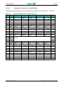
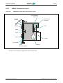
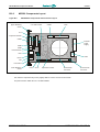
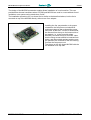
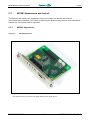
1
CPC502 3U CompactPCI Intel Pentium M Based Processor Module User Manual Rev. 0.02 E February 2006 The product described in this manual is compliant to all related CE standards. Product Title: CPC502 Document name: CPC502 User Manual Manual version: 0.02 E Copyright © 2005, 2006 Fastwel Co. Ltd. All rights reserved. Revision Record Rev. Index Brief Description Product Index Date 0.01 Initial version CPC502, RIO582, MIC580, RIO583 June 2005 0.01a Minor improvements and corrections, text rearrangements CPC502, RIO582, MIC580, RIO583 October 2005 0.02 Total text reassertion CPC502, RIO582, MIC580, RIO583 January 2006 Contact Information Fastwel Co. Ltd. Address: Tel.: Fax: E-mail: 108 Profsoyuznaya st., Moscow 117437, Russian Federation +7 (095) 234-0639 +7 (095) 232-1654 [email protected] For more details, please visit our Web-site: http://www.fastwel.com/ CPC502 Table of Contents Table of Contents.................................................................................................................................................. 0-1 List of Tables......................................................................................................................................................... 0-4 List of Figures ....................................................................................................................................................... 0-5 Notation Conventions............................................................................................................................................ 0-6 General Safety Precautions .................................................................................................................................. 0-7 Unpacking, Inspection and Handling..................................................................................................................... 0-8 Three Year Warranty .......................................................................................................................................... 0-10 1 Introduction......................................................................................................................................... 1-1 1.1 1.2 1.3 1.4 1.5 1.6 1.7 2 Overview.................................................................................................................................................... 1-1 CPC502 Versions ...................................................................................................................................... 1-3 CPC502 Diagrams..................................................................................................................................... 1-4 1.3.1 Block Diagram .......................................................................................................................... 1-5 1.3.2 Module Appearance.................................................................................................................. 1-6 1.3.3 Module Layout .......................................................................................................................... 1-7 1.3.4 Front Panel ............................................................................................................................... 1-8 Technical Characteristics........................................................................................................................... 1-9 1.4.1 Processor, Memory and Chipset............................................................................................... 1-9 1.4.2 Interfaces ................................................................................................................................ 1-10 1.4.3 Control and Monitoring............................................................................................................ 1-12 1.4.4 General ................................................................................................................................... 1-12 1.4.5 Software.................................................................................................................................. 1-13 Information for Application Developers .................................................................................................... 1-13 Delivery Checklist .................................................................................................................................... 1-13 System Expansion Modules .................................................................................................................... 1-14 1.7.1 RIO582 Rear I/O Module ........................................................................................................ 1-14 1.7.2 MIC580 Mezzanine Interface Module ..................................................................................... 1-15 1.7.3 MIC583 Mezzanine Interface Module ..................................................................................... 1-15 Detailed Description........................................................................................................................... 2-1 2.1 2.2 2.3 C P C 5 0 2 Processor, Memory and Chipset................................................................................................................ 2-1 2.1.1 Processor.................................................................................................................................. 2-1 2.1.2 System Memory........................................................................................................................ 2-1 2.1.3 Chipset...................................................................................................................................... 2-1 Internal Peripherals.................................................................................................................................... 2-3 2.2.1 Flash Memory ........................................................................................................................... 2-3 2.2.1.1 Solid-State Disk (SSD)............................................................................................. 2-3 2.2.1.2 CompactFlash.......................................................................................................... 2-3 2.2.1.3 FRAM Emergency Storage for User Data................................................................ 2-3 2.2.2 Timers....................................................................................................................................... 2-3 2.2.3 Watchdog Timer ....................................................................................................................... 2-4 2.2.3.1 Internal Function Registers Bits ............................................................................... 2-4 2.2.3.2 Watchdog Timer Programming ................................................................................ 2-5 2.2.4 Local SMBus Devices ............................................................................................................... 2-6 2.2.4.1 Temperatures Monitoring ......................................................................................... 2-6 2.2.4.2 Serial EEPROM ....................................................................................................... 2-6 2.2.5 Reset ........................................................................................................................................ 2-6 2.2.6 Battery ...................................................................................................................................... 2-6 Module Interfaces ...................................................................................................................................... 2-7 2.3.1 Keyboard/Mouse Interface........................................................................................................ 2-7 2.3.2 Serial Interfaces (RS232).......................................................................................................... 2-7 U s e r M a n u a l 0-1 © 2 0 0 6 F a s t w e l V e r . 0 0 2 E CPC502 2.3.3 2.3.4 2.3.5 2.3.6 2.3.7 2.3.8 2.3.9 2.3.10 2.3.11 3 Installation........................................................................................................................................... 3-1 3.1 3.2 3.3 3.4 4 Safety Regulations..................................................................................................................................... 3-1 Installation Procedure ................................................................................................................................ 3-2 Removal Procedure ................................................................................................................................... 3-3 Peripheral Devices Installation .................................................................................................................. 3-3 3.4.1 USB Devices Installation........................................................................................................... 3-3 3.4.2 CompactFlash Cards Installation .............................................................................................. 3-4 3.4.3 Battery Replacement ................................................................................................................ 3-5 3.4.4 Expansion Modules Installation ................................................................................................ 3-5 Configuration ...................................................................................................................................... 4-1 4.1 Interrupts Handling .................................................................................................................................... 4-1 4.1.1 On-board PCI Interrupts............................................................................................................ 4-2 Memory Maps ............................................................................................................................................ 4-2 4.2.1 First Megabyte Memory Map .................................................................................................... 4-2 4.2.2 I/O Addresses ........................................................................................................................... 4-3 4.2 5 Phoenix® BIOS Setup ........................................................................................................................ 5-1 5.1 6 Boot Details ............................................................................................................................................... 5-1 5.1.1 Booting without a Monitor, Keyboard or Mouse ........................................................................ 5-1 5.1.2 Booting from USB ..................................................................................................................... 5-1 Thermal and Power Issues ................................................................................................................ 6-1 6.1 Temperature Control.................................................................................................................................. 6-1 6.1.1 Passive Regulation ................................................................................................................... 6-1 6.1.2 Active Regulation...................................................................................................................... 6-2 System Power ........................................................................................................................................... 6-3 6.2 A USB Interfaces.......................................................................................................................... 2-7 2.3.3.1 USB Connectors USB1 and USB2 Pinouts (CPC502 front panel) ........................... 2-7 Graphics Controller ................................................................................................................... 2-8 2.3.4.1 DVM Technology ..................................................................................................... 2-8 2.3.4.2 Supported Resolutions............................................................................................. 2-9 2.3.4.3 CRT Interface and Connector .................................................................................. 2-9 Parallel Port Interface ............................................................................................................. 2-10 Gigabit Ethernet...................................................................................................................... 2-10 2.3.6.1 RJ45 Connectors Pinout ........................................................................................ 2-10 CompactFlash Socket............................................................................................................. 2-11 EIDE Interface ........................................................................................................................ 2-12 Floppy Drive Interface............................................................................................................. 2-12 LED Indicators ........................................................................................................................ 2-12 2.3.10.1 L2 Green LED Control ........................................................................................... 2-12 CompactPCI Bus Connectors ................................................................................................. 2-13 2.3.11.1 CompactPCI Connector Color Coding ................................................................... 2-13 2.3.11.2 CompactPCI Connectors J1 and J2 Pinouts .......................................................... 2-14 2.3.11.3 Rear I/O Interfaces................................................................................................. 2-16 RIO582 Rear I/O Module.....................................................................................................................A-1 A.1 C P C 5 0 2 Introduction................................................................................................................................................A-1 A.1.1 RIO582 Versions ......................................................................................................................A-1 A.1.2 RIO582 Delivery Checklist ........................................................................................................A-2 A.1.3 Mechanical Specifications.........................................................................................................A-2 U s e r M a n u a l 0-2 © 2 0 0 6 F a s t w e l V e r . 0 0 2 E CPC502 A.2 A.3 A.4 B RIO582 Appearance and Layout ...............................................................................................................A-3 A.2.1 RIO582 Appearance .................................................................................................................A-3 A.2.2 RIO582 Components Layout ....................................................................................................A-4 RIO582 Interfaces......................................................................................................................................A-5 A.3.1 RIO582 Interfaces List (4HP)....................................................................................................A-5 A.3.1.1 Front Panel Interfaces..............................................................................................A-5 A.3.1.2 Internal Interfaces ....................................................................................................A-5 A.3.2 RIO582 Interfaces Detailed Description....................................................................................A-6 A.3.2.1 VGA-CRT Interface..................................................................................................A-6 A.3.2.2 USB Interfaces.........................................................................................................A-7 A.3.2.3 COM1 Serial Port.....................................................................................................A-8 A.3.2.4 External Fan Connector ...........................................................................................A-9 A.3.2.5 Serial ATA Port ........................................................................................................A-9 A.3.2.6 J10 Expansion Header.............................................................................................A-9 A.3.2.7 CompactPCI Interface............................................................................................A-10 Installation of RIO582 and Peripheral Devices ........................................................................................A-11 A.4.1 RIO582 Installation Procedures ..............................................................................................A-11 A.4.2 RIO582 Removal Procedures .................................................................................................A-12 A.4.3 Battery Replacement ..............................................................................................................A-12 A.4.4 USB Devices Connection........................................................................................................A-12 A.4.5 Expansion Modules and External Devices Installation............................................................A-13 MIC580 Mezzanine Expansion Module.............................................................................................B-1 B.1 B.2 B.3 B.4 C P C 5 0 2 Introduction................................................................................................................................................B-1 B.1.1 MIC580 Versions ......................................................................................................................B-1 B.1.2 MIC580 Delivery Checklist........................................................................................................B-2 B.1.3 Mechanical Specifications.........................................................................................................B-2 MIC580 Appearance and Layout ...............................................................................................................B-3 B.2.1 MIC580 Appearance .................................................................................................................B-3 B.2.2 MIC580 Components Layout ....................................................................................................B-5 MIC580 Interfaces .....................................................................................................................................B-6 B.3.1 MIC580 Interfaces List ..............................................................................................................B-6 B.3.1.1 Front Panel (4HP) Interfaces ...................................................................................B-6 B.3.1.2 Internal Interfaces ....................................................................................................B-6 B.3.2 MIC580 Interfaces Detailed Description....................................................................................B-7 B.3.2.1 Serial Interfaces .......................................................................................................B-7 B.3.2.2 USB Interfaces.........................................................................................................B-8 B.3.2.3 PS/2 Keyboard/Mouse Interface ..............................................................................B-9 B.3.2.4 Audio Interface.......................................................................................................B-10 B.3.2.5 L3 and L4 LED Indicators ......................................................................................B-11 B.3.2.6 LPT Interface .........................................................................................................B-13 B.3.2.7 Floppy Drive Interface............................................................................................B-14 B.3.2.8 External Power Supply Connector .........................................................................B-15 B.3.2.9 SerialATA Port .......................................................................................................B-16 B.3.2.10 HDD Connector for External EIDE Devices ...........................................................B-17 B.3.2.11 HDD 2.5" Connector for Onboard Disk Installation ................................................B-18 B.3.2.12 Onboard Fan Connector ........................................................................................B-19 B.3.2.13 Expansion Headers................................................................................................B-19 MIC580 Installation ..................................................................................................................................B-20 B.4.1 2.5" HDD or Onboard Fan Installation on MIC580 ..................................................................B-20 B.4.2 MIC580 Installation on CPC502..............................................................................................B-23 U s e r M a n u a l 0-3 © 2 0 0 6 F a s t w e l V e r . 0 0 2 E CPC502 C MIC583 Mezzanine Expansion Module.............................................................................................C-1 C.1 C.2 C.3 C.4 D Supplementary Information...............................................................................................................D-1 D.1 E Introduction................................................................................................................................................C-1 C.1.1 MIC583 Versions ......................................................................................................................C-1 C.1.2 MIC583 Delivery Checklist........................................................................................................C-2 C.1.3 Mechanical Specifications.........................................................................................................C-2 MIC583 Appearance and Layout ...............................................................................................................C-3 C.2.1 MIC583 Appearance .................................................................................................................C-3 C.2.2 MIC583 Components Layout ....................................................................................................C-4 MIC583 Interfaces .....................................................................................................................................C-5 C.3.1 MIC583 Interfaces List (4HP)....................................................................................................C-5 C.3.1.1 Front Panel Interfaces..............................................................................................C-5 C.3.1.2 Internal Interfaces ....................................................................................................C-5 C.3.2 MIC583 Interfaces Detailed Description....................................................................................C-5 C.3.2.1 Isolated Reset Connector ........................................................................................C-5 C.3.2.2 LVDS Interface.........................................................................................................C-6 C.3.2.3 Audio Interface.........................................................................................................C-7 MIC583 Installation ....................................................................................................................................C-8 Related Standards and Specifications .......................................................................................................D-1 Useful Abbreviations, Acronyms and Short-cuts ...........................................................................E-1 List of Tables Table 1-1: Table 2-1: Table 2-2: Table 2-3: Table 2-4: Table 2-5: Table 2-6: Table 2-7: Table 2-8: Table 2-9: Table 4-1: Table 4-2: Table 4-3: Table 4-4: Table 6-1: Table 6-2: Table A-1: Table A-2: Table A-3: Table A-4: Table A-5: Table A-6: Table A-7: Table B-1: Table B-2: Table B-3: Table B-4: Table B-5: Table B-6: Table B-7: Table B-8: C P C 5 0 2 Expansion Interface Modules Ordering Numbers and Differences .......................................................... 1-14 SMBus Devices ......................................................................................................................................... 2-6 USB1 and USB2 Pinouts (CPC502 Front Panel)....................................................................................... 2-7 Supported Display Modes.......................................................................................................................... 2-9 CPC502: SVGA Front Panel Connector Pinout ......................................................................................... 2-9 Gigabit Ethernet Connectors Pinouts....................................................................................................... 2-10 CompactFlash Socket Pinout .................................................................................................................. 2-11 CompactPCI Connector Coding Colors ................................................................................................... 2-13 CompactPCI Bus Connector J1 System Slot Pinout................................................................................ 2-14 32-bit CompactPCI Bus Connector J2 System Slot Pinout...................................................................... 2-15 Interrupt Settings ....................................................................................................................................... 4-1 PCI Interrupt Routing ................................................................................................................................. 4-2 First Megabyte Memory Map ..................................................................................................................... 4-2 I/O Address Map........................................................................................................................................ 4-3 DC Input Voltage Ranges and Limits......................................................................................................... 6-3 Some CPC502 Components Power Consumption .................................................................................... 6-3 RIO582 Versions Differences ................................................................................................................... A-1 VGA J2 Connector Pinout......................................................................................................................... A-6 USB5 and USB6 Connectors Pinouts....................................................................................................... A-7 COM1 J4 Serial Port Connector Pinout .................................................................................................... A-8 J9 External Fan Connector Pinout ............................................................................................................ A-9 J8 SATA Connector Pinout....................................................................................................................... A-9 RIO582 J1 CompactPCI Connector Pinout..............................................................................................A-10 MIC580 Versions Differences ................................................................................................................... B-1 COM2 Serial Port Connector Pinout ......................................................................................................... B-7 COM3 Serial Port Connector Pinout ......................................................................................................... B-8 USB3 and USB4 Connectors Pinouts....................................................................................................... B-8 PS/2 CON14 Keyboard/Mouse Connector Pinout .................................................................................... B-9 "CD In" Connector Pinout ........................................................................................................................B-10 "Aux In" Connector Pinout .......................................................................................................................B-10 LPT Connector Pinout .............................................................................................................................B-13 U s e r M a n u a l 0-4 © 2 0 0 6 F a s t w e l V e r . 0 0 2 E CPC502 Table B-9: Table B-10: Table B-11: Table B-12: Table B-13: Table B-14: Table C-1: Table C-2: Table C-3: Table C-4: Table C-5: Table D-1: Table D-2: FDD Connector Pinout.............................................................................................................................B-14 ATX Power Supply Connector Pinout ......................................................................................................B-15 SerialATA Connector Pinout ....................................................................................................................B-16 Standard EIDE HDD Connector Pinout ...................................................................................................B-17 EIDE HDD 2.5" Connector Pinout............................................................................................................B-18 Onboard Fan Connector Pinout ...............................................................................................................B-19 MIC583 Versions Differences ................................................................................................................... C-1 LVDS J3 Connector Pinout....................................................................................................................... C-6 MIC583 Audio Interface Connectors......................................................................................................... C-7 "CD In" Connector Pinout ......................................................................................................................... C-7 "Line Out" Connector Pinout ..................................................................................................................... C-7 Related Standards .................................................................................................................................... D-1 Related Specifications .............................................................................................................................. D-1 List of Figures Figure 1-1: Figure 1-2: Figure 1-3: Figure 1-4: Figure 2-1: Figure A-1: Figure A-2: Figure A-3: Figure A-4: Figure A-5: Figure B-1: Figure B-2: Figure B-3: Figure B-4: Figure B-5: Figure B-6: Figure B-7: Figure B-8: Figure B-9: Figure B-10: Figure B-11: Figure C-1: Figure C-2: Figure C-3: CPC502 Block Diagram............................................................................................................................. 1-5 CPC502 Module Appearance .................................................................................................................... 1-6 CPC502 Module Layout............................................................................................................................. 1-7 CPC502 4HP Front Panel.......................................................................................................................... 1-8 CompactPCI Connectors J1 and J2 .................................................................................................... 2-13 RIO582 Appearance ................................................................................................................................. A-3 RIO582 Main Components and Connectors Layout ................................................................................. A-4 D-Sub VGA-CRT J2 Connector ................................................................................................................ A-6 USB5 and USB6 Connectors.................................................................................................................... A-7 D-Sub J4 Connector of the COM1 Serial Port .......................................................................................... A-8 MIC580 Appearance with a Cooling Fan Installed .................................................................................... B-3 MIC580 Appearance with a 2.5" HDD Installed ........................................................................................ B-4 MIC580 Main Components and Connectors Layout ................................................................................. B-5 D-Sub Connector of the COM2 Serial Port ............................................................................................... B-7 USB3 and USB4 Connectors.................................................................................................................... B-8 PS/2 Keyboard/Mouse Connector ............................................................................................................ B-9 External ATX Power Supply Connector ...................................................................................................B-15 SerialATA Connector ...............................................................................................................................B-16 HDD Connector .......................................................................................................................................B-17 2.5" HDD Connector ................................................................................................................................B-18 Onboard Fan Connector (FAN) ...............................................................................................................B-19 MIC583 Appearance................................................................................................................................. C-3 MIC583 Main Components and Connectors Layout ................................................................................. C-4 LVDS J3 Connector .................................................................................................................................. C-6 All information in this document is provided for reference only, with no warranty of its suitability for any specific purpose. This information has been thoroughly checked and is believed to be entirely reliable and consistent with the product that it describes. However, Fastwel accepts no responsibility for inaccuracies, omissions or their consequences, as well as liability arising from the use or application of any product or example described in this document. Fastwel Co. Ltd. reserves the right to change, modify, and improve this document or the products described in it, at Fastwel's discretion without further notice. Software described in this document is provided on an “as is” basis without warranty. Fastwel assumes no liability for consequential or incidental damages originated by the use of this software. This document contains information, which is property of Fastwel Co. Ltd. It is not allowed to reproduce it or transmit by any means, to translate the document or to convert it to any electronic form in full or in parts without antecedent written approval of Fastwel Co. Ltd. or one of its officially authorized agents. Fastwel and Fastwel logo are trademarks owned by Fastwel Co. Ltd., Moscow, Russian Federation. CompactPCI is a trademark of the PCI industrial Computers Manufacturers Group. Ethernet is a registered trademark of Xerox Corporation. IEEE is a registered trademark of the Institute of Electrical and Electronics Engineers Inc. Intel is a trademark of Intel Corporation. Pentium M and Celeron M are trademarks of Intel Corporation. Microsoft is a trademark of the Microsoft corporation. In addition, this document may include names, company logos and trademarks, which are registered trademarks and, therefore, are property of their respective owners. Fastwel welcomes suggestions, remarks and proposals regarding the form and the content of this Manual. C P C 5 0 2 U s e r M a n u a l 0-5 © 2 0 0 6 F a s t w e l V e r . 0 0 2 E CPC502 Notation Conventions Warning, ESD Sensitive Device! This symbol draws your attention to the information related to electro static sensitivity of your product and its components. To keep product safety and operability it is necessary to handle it with care and follow the ESD safety directions. Warning! This sign marks warnings about hot surfaces. The surface of the heatsink and some components can get very hot during operation. Take due care when handling, avoid touching hot surfaces! Caution: Electric Shock! This symbol warns about danger of electrical shock (> 60 V) when touching products or parts of them. Failure to observe the indicated precautions and directions may expose your life to danger and may lead to damage to your product. Warning! Information marked by this symbol is essential for human and equipment safety. Read this information attentively, be watchful. Note... This symbol and title marks important information to be read attentively for your own benefit. C P C 5 0 2 U s e r M a n u a l 0-6 © 2 0 0 6 F a s t w e l V e r . 0 0 2 E CPC502 General Safety Precautions This product was developed for fault-free operation. Its design provides conformance to all related safety requirements. However, the life of this product can be seriously shortened by improper handling and incorrect operation. That is why it is necessary to follow general safety and operational instructions below. Warning! All operations on this device must be carried out by sufficiently skilled personnel only. Warning! When handling this product, special care must be taken not to hit the heatsink (if installed) against another rigid object. Also, be careful not to drop the product, since this may cause damage to the heatsink, CPU or other sensitive components as well. Please, keep in mind that any physical damage to this product is not covered under warranty. Note: This product is guaranteed to operate within the published temperature ranges and relevant conditions. However, prolonged operation near the maximum temperature is not recommended by Fastwel or by electronic chip manufacturers due to thermal stress related failure mechanisms. These mechanisms are common to all silicon devices, they can reduce the MTBF of the product by increasing the failure probability. Prolonged operation at the lower limits of the temperature ranges has no limitations. Caution, Electric Shock! Before installing this product into a system and before installing other devices on it, always ensure that your mains power is switched off. Always disconnect external power supply cables during all handling and maintenance operations with this module to avoid serious danger of electrical shock. C P C 5 0 2 U s e r M a n u a l 0-7 © 2 0 0 6 F a s t w e l V e r . 0 0 2 E CPC502 Unpacking, Inspection and Handling Please read the manual carefully before unpacking the module or mounting the device into your system. Keep in mind the following: ESD Sensitive Device! Electronic modules and their components are sensitive to static electricity. Even a non-perceptible by human being static discharge can be sufficient to destroy or degrade a component's operation! Therefore, all handling operations and inspections of this product must be performed with due care, in order to keep product integrity and operability: Preferably, unpack or pack this product only at EOS/ESD safe workplaces. Otherwise, it is important to be electrically discharged before touching the product. This can be done by touching a metal part of your system case with your hand or tool. It is particularly important to observe anti-static precautions when setting jumpers or replacing components. If the product contains batteries for RTC or memory back-up, ensure that the module is not placed on conductive surfaces, including anti-static mats or sponges. This can cause shortcircuit and result in damage to the battery and other components. Store this product in its protective packaging while it is not used for operational purposes. Unpacking The product is carefully packed in an antistatic bag and in a carton box to protect it against possible damage and harmful influence during shipping. Unpack the product indoors only at a temperature not less than +15°C and relative humidity not more than 70%. Please note, that if the product was exposed to the temperatures below 0°С for a long time, it is necessary to keep it at normal conditions for at least 24 hours before unpacking. Do not keep the product close to a heat source. Following ESD precautions, carefully take the product out of the shipping carton box. Proper handling of the product is critical to ensure correct operation and long-term reliability. When unpacking the product, and whenever handling it thereafter, be sure to hold the module preferably by the front panel, card edges or ejector handles. Avoid touching the components and connectors. Retain all original packaging at least until the warranty period is over. You may need it for shipments or for storage of the product. Initial Inspection Although the product is carefully packaged, it is still possible that shipping damages may occur. Careful inspection of the shipping carton can reveal evidence of damage or rough handling. Should you notice that the package is damaged, please notify the shipping service and the manufacturer as soon as possible. Retain the damaged packing material for inspection. After unpacking the product, you should inspect it for visible damage that could have occurred during shipping or unpacking. If damage is observed (usually in the form of bent component leads or loose socketed components), contact Fastwel's official distributor from which you have purchased the product for additional instructions. Depending on the severity of the damage, the product may even need to be returned to the factory for repair. DO NOT apply power to the product if it has visible damage. Doing so may cause further, possibly irreparable damage, as well as result in a fire or electric shock hazard. If the product contains socketed components, they should be inspected to make sure they are seated fully in their sockets. C P C 5 0 2 U s e r M a n u a l 0-8 © 2 0 0 6 F a s t w e l V e r . 0 0 2 E CPC502 Handling In performing all necessary installation and application operations, please follow only the instructions supplied by the present manual. In order to keep Fastwel’s warranty, you must not change or modify this product in any way, other than specifically approved by Fastwel or described in this manual. Technical characteristics of the systems in which this product is installed, such as operating temperature ranges and power supply parameters, should conform to the requirements stated by this document. Retain all the original packaging, you will need it to pack the product for shipping in warranty cases or for safe storage. Please, pack the product for transportation in the way it was packed by the supplier. When handling the product, please, remember that the module, its components and connectors require delicate care. Always keep in mind the ESD sensitivity of the product. C P C 5 0 2 U s e r M a n u a l 0-9 © 2 0 0 6 F a s t w e l V e r . 0 0 2 E CPC502 Three Year Warranty Fastwel Co. Ltd. (Fastwel), warrants that its standard hardware products will be free from defects in materials and workmanship under normal use and service for the currently established warranty period. Fastwel’s only responsibility under this warranty is, at its option, to replace or repair any defective component part of such products free of charge. Fastwel neither assumes nor authorizes any other liability in connection with the sale, installation or use of its products. Fastwel shall have no liability for direct or consequential damages of any kind arising out of sale, delay in delivery, installation, or use of its products. If a product should fail through Fastwel's fault during the warranty period, it will be repaired free of charge. For out of warranty repairs, the customer will be invoiced for repair charges at current standard labor and materials rates. Warranty period for Fastwel products is 36 months since the date of purchase. The warranty set forth above does not extend to and shall not apply to: 1. Products, including software, which have been repaired or altered by other than Fastwel personnel, unless Buyer has properly altered or repaired the products in accordance with procedures previously approved in writing by Fastwel. 2. Products, which have been subject to power, supply reversal, misuse, neglect, accident, or improper installation. Returning a product for repair 1. Apply to Fastwel company or to any of the Fastwel's official representatives for the Product Return Authorization. 2. Attach a failure inspection report with a product to be returned in the form, accepted by customer, with a description of the failure circumstances and symptoms. 3. Carefully package the product in the antistatic bag, in which the product had been supplied. Failure to package in antistatic material will VOID all warranties. Then package the product in a safe container for shipping. 4. The customer pays for shipping the product to Fastwel or to an official Fastwel representative or dealer. C P C 5 0 2 U s e r M a n u a l 0-10 © 2 0 0 6 F a s t w e l V e r . 0 0 2 E Chapter 1 Introduction T h i s p a g e w a s i n t e n t i o n a l l y l e f t b l a n k . Introduction CPC502 1 Introduction 1.1 Overview The product described in this Manual is a CompactPCI / PXI processor module CPC502. To get the details about the CompactPCI, a wide spread industrial standard, please refer to PCI and CompactPCI specifications. The Internet site of the PCI Industrial Computer Manufacturers Group (PICMG) provides information related to these standards (http://www.picmg.org/). CPC502 supports both CompactPCI and PXI standards for 32-bit 33 MHz bus, which allow to build flexible high-performance systems. Dual standard support includes possibility to install mezzanine expansion modules both on the top and on the bottom side of the processor module. CPC502 is based on Intel Pentium M processor in the µFCPGA478 or µFCBGA479 packages operating at the processor speed of up to 2 GHz and a Processor Side Bus (PSB) running at 400 MHz. The Intel Pentium M processor core with integrated 64 KB L1 and up to 2048 KB L2 cache provides its unique performance to power consumption ratio. The CPC502 utilizes the chipset which includes Intel 82855GME GMCH and Hance Rapid (6300ESB) ICH. The board includes up to 1 GB of soldered Double Data Rate (DDR) memory with ECC operated at 333 MHz. System features include two Gigabit Ethernet ports and a built-in Intel 2D/3D Graphics accelerator with up to 64 MB memory shared with system for enhanced graphics performance with VGA CRTdisplay and with TFT LVDS interfaces. The CPC502 comes with the following PC interfaces including: six USB 2.0 ports, four COM ports, two EIDE ATA100 interfaces, one CompactFlash Type I/II socket, one Floppy port, one parallel port, and, moreover, two CompactPCI bus standard connectors J1 and J2 at the rear side of the card. CPC502 employs the thoroughly selected components for embedded industrial systems to ensure their long term availability. The board is compatible with the Microsoft® Windows® 2000/XP/CE, QNX and Linux® operating systems. C P C 5 0 2 U s e r M a n u a l 1-1 © 2 0 0 6 F a s t w e l V e r . 0 0 2 E Introduction CPC502 Some of the CPC502's outstanding features are: Intel® Pentium® M processor family, up to 2.0 GHz Up to 2 MB L2 on-die cache running at CPU speed 82855GME GMCH and 6300ESB (Hance Rapid) ICH chipset 400 MHz processor system bus Up to 1 GB of soldered DDR SDRAM memory running at 333 MHz with ECC CompactPCI bus: 32-bit / 33 MHz Integrated 3D high performance VGA controller 64 MB memory shared with system CRT-displays support with resolutions of up to 2048 x 1536 pixels at 16 bits and 75 Hz LVDS interface support via Rear I/O Two Gigabit Ethernet interfaces (via PCI-X bus): 10Base-T, 100Base-TX, and 1000Base-T Two EIDE Ultra ATA/100 interfaces Onboard CompactFlash Type I/II socket Three serial ports (*) Up to six USB 2.0 ports (*) PS/2 keyboard and mouse interface (*) Floppy disk interface (*) Parallel port (*) Hardware Monitor (LM82) Watchdog timer Additional counters and timers integrated in the ICH Real-time clock with battery backup Two automatically switchable 1 MB on-board FWHs (one for work copy of BIOS and one for reserve copy of BIOS) 4HP, 3U CompactPCI form-factor Hotswap capability: as system controller Rear I/O on J2 Passive or active heatsink solution Phoenix® BIOS (*) – Available either on the CPC502, on Rear I/O or on mezzanine modules C P C 5 0 2 U s e r M a n u a l 1-2 © 2 0 0 6 F a s t w e l V e r . 0 0 2 E Introduction 1.2 CPC502 CPC502 Versions At the present time, the module is offered in flexible configuration. The options include different processors, the size of soldered system memory, and other options described in this section. Moreover, the CPC502 processor module can be delivered together with the MIC580 mezzanine expansion module. Supplemented with a standard ATX power supply unit, the assembly consisting of these two modules can be used as a space-saving stand-alone "computing brick" providing system developers with additional design opportunities. All variants are available in two versions, for industrial (-40°C to +85°C) and for commercial (0°C to 70°C) temperature ranges. Other configuration options are available upon request. The customer can choose necessary configuration options using the following template: 1 – 1 2 – 3 – 4 – 5 Basic product name: CPC502 2 Processor: P1.1 P1.4 P1.6 P1.8 3 Soldered system memory: RAM512 RAM1024 4 5 Pentium M 1.1 GHz, ULV, 400 MHz FSB Pentium M 1.4 GHz, 400 MHz FSB Pentium M 1.6 GHz, 400 MHz FSB Pentium M 1.8 GHz, 400 MHz FSB 512 MB soldered DDR SDRAM 1024 MB soldered DDR SDRAM Operating temperature range: I Industrial, -40°C to +85°C C Commercial, 0°C to 70°C Other options: CompactFlash Module \CF128 \CF256 \CF512 \CF1024 128 MB CompactFlash card, industrial 256 MB CompactFlash card, industrial 512 MB CompactFlash card, industrial 1024 MB CompactFlash card, industrial CPC502 assembled with MIC580 \MIC580IR \MIC580CR \MIC580IL \MIC580CL Mezzanine MIC580 Right Mounted (CPCI), Industrial Range Mezzanine MIC580 Right Mounted (CPCI), Commercial Range Mezzanine MIC580 Left Mounted (PXI), Industrial Range Mezzanine MIC580 Left Mounted (PXI), Commercial Range Options for MIC580 only: \HDD20 \FFD2048 \FAN 2.5" Hard Disk Drive, 20 GB 2.5" Flash Disk, 2048 MB Fan installed on MIC580 (for CPC502 active cooling) Coating \COATED Protective Coating C P C 5 0 2 U s e r M a n u a l 1-3 © 2 0 0 6 F a s t w e l V e r . 0 0 2 E Introduction CPC502 Operating System \DOS \XPE \QNX \WCE \LNX DOS Windows XP Embedded QNX Windows CE 5.0 Linux 2.4.20 Example: CPC502 – P1.6 – RAM512 – C \CF128 \MIC580CR \HDD20 \COATED \XPE 3U CompactPCI Pentium M SBC, FFD 32 MB, VGA, 2x Gigabit Ethernet Pentium M 1.6 GHz, 400 MHz FSB 512 MB soldered DDR SDRAM Commercial operating temperature range, 0°C to +70°C 128 MB CompactFlash card Mezzanine MIC580 right mounted (cPCI), commercial range 2.5" HDD 20 GB Protective coating Windows XP Embedded 1.3 CPC502 Diagrams The diagrams in this section give visual information about the CPC502 module design, its appearance, connectors and components layout. The diagrams may not reflect insignificant differences between the CPC502 versions. C P C 5 0 2 U s e r M a n u a l 1-4 © 2 0 0 6 F a s t w e l V e r . 0 0 2 E Introduction Block Diagram Figure 1-1: CPC502 Block Diagram Hardware Monitor Intel Pentium M or Celeron M CK-408 & SS Clocking VGA CRT VGA CRT PSB 400 MHz LVDS TFT Front Panel 855GME GMCH CPCI RIO: J2 1.3.1 CPC502 Mezzanine Connector Soldered DDR SDRAM up to 1 GB EIDE1 SATA 1 CFII FWH PXI Interface PCI-X Bus Dual Port Gigabit Ethernet PCI 32bit Bus COM Port 1 Hance Rapid ICH FWH SSD 32Mb (Up To 1Gb) USB Port 4 LPC Interface USB Port 3 AC97 Link CPLD AC97 Link 10/100/1000 BaseT 10/100/1000 BaseT USB Ports 1, 2 SATA 2 HUB Inerface PCI-PCI Bridge GMCH VR PCI 32bit Bus CPCI: J1 CPU Core VR PCI BUS 32-bit Mezzanine Connector DDR VR Power Supply C P C 5 0 2 U s e r M a n u a l 1-5 © 2 0 0 6 F a s t w e l V e r . 0 0 2 E Introduction 1.3.2 CPC502 Module Appearance Figure 1-2: CPC502 Module Appearance The appearance may vary for different versions of the module. C P C 5 0 2 U s e r M a n u a l 1-6 © 2 0 0 6 F a s t w e l V e r . 0 0 2 E Introduction 1.3.3 CPC502 Module Layout Figure 1-3: CPC502 Module Layout Hance Rapid ICH (bottom side) Upper Retaining Screw CompactFlash Socket GMCH Heat Sink (not shown) Front Panel J11: Expansion Connector J2 cPCI SVGA CPU USB1 USB2 LED indicators L1 and L2 J1 cPCI GigabitEthernet Sockets Ejector Handle Hotswap Switch Connector (SW1) Li Battery J10: Expansion Connector Memory Chips The layout may slightly differ for various versions of the module. C P C 5 0 2 U s e r M a n u a l 1-7 © 2 0 0 6 F a s t w e l V e r . 0 0 2 E Introduction 1.3.4 CPC502 Front Panel Figure 1-4: CPC502 4HP Front Panel Upper Retaining Screw GigabitEthernet 2 Socket L1 USB2 USB1 L2 Eth1 GigabitEthernet 1 Socket USB Sockets L2 LED Indicator (green) Eth2 L1 LED Indicator (red) SVGA SVGA Connector Ejector Handle Lower Retaining Screw The appearance may slightly differ for various versions of the module. C P C 5 0 2 U s e r M a n u a l 1-8 © 2 0 0 6 F a s t w e l V e r . 0 0 2 E Introduction CPC502 1.4 Technical Characteristics 1.4.1 Processor, Memory and Chipset CPU The CPC502 supports the following Intel processors: Pentium® M Processor Up to 2.0 GHz Up to 2 MB L2 on-die cache 400 MHz PSB Supports SpeedStep® III for low power mode Ultra Low Voltage Pentium® M Processor Up to 1.4 GHz Up to 2 MB L2 on-die cache 400 MHz PSB Supports SpeedStep® III for low power mode Memory Main memory: Up to 1 GB of soldered DDR SDRAM memory, ECC support Memory frequency: 333 MHz (PC2700) Flash memory: Two flash memory Firmware Hubs (a part of the chipset): 1 MB FWH for working copy and 1 MB FWH for reserve copy of BIOS One 256 byte EEPROM for storing CMOS data when operating without battery 32 MB solid-state disk (NAND flash memory) with Fastwel file system Chipset Intel® 82855GME Graphics and Memory Controller Hub (GMCH) Support for a single Pentium M family microprocessor 64-bit AGTL/AGTL+ based PSB interface at 400 MHz 64-bit System Memory interface, optimized for DDR SDRAM memory operating at 333 MHz with additional 8-bits for ECC Integrated 2D/3D Graphics and H/W Motion Compensation Engines Integrated DAC, 350 MHz C P C 5 0 2 U s e r M a n u a l 1-9 © 2 0 0 6 F a s t w e l V e r . 0 0 2 E Introduction CPC502 Intel® 82801DB I/O Controller Hub (ICH4) PCI Rev. 2.2 compliant with support for 33 MHz/32-bit PCI bus Enhanced DMA controller, interrupt controller, and timer Integrated IDE controller Ultra ATA100 USB 2.0 host interface PCI-X 64-bit interface Serial ATA controller AC'97 audio interface System Management Bus Power management logic support Low Pin Count (LPC) interface Firmware Hub (FWH) interface support Additional timers 1.4.2 Interfaces CompactPCI Bus Interface Compliant with CompactPCI Specification PICMG® 2.0 R3.0 System master operation 32-bit / 33 MHz master interface 3.3V / 5.0V compatible Serial Ports COM2 and COM3 (available via MIC580): COM2 – RS-232, 9-pin D-sub connector on the front panel COM3 – RS-232, 10-pin onboard IDC connector 16C550 compatible UARTs COM1 (available via RIO582): 16C550 compatible UART Rear I/O availability only Opto-isolated USB Interface Up to six USB 2.0 ports supporting UHCI and EHCI: Two USB type A connectors on the CPC502 front panel Two connectors on RIO582 Two connectors on MIC580 Parallel Port Multi-Mode™ parallel port, SPP/ECP/EPP compatible Standard Mode IBM PC/XT, PC/AT, and PS/2 compatible bidirectional parallel port Available via MIC580 only C P C 5 0 2 U s e r M a n u a l 1-10 © 2 0 0 6 F a s t w e l V e r . 0 0 2 E Introduction CPC502 Gigabit Ethernet Two 10/100/1000 Mb/s Gigabit Ethernet interfaces based on the Intel 82546GB Ethernet PCI-X bus controller. Two RJ45 connectors on CPC502 front panel Automatic mode recognition Automatic cabling configuration recognition Cabling requirement: Category 5, UTP, four-pair cabling VGA interface Built-in Intel 2D/3D high performance graphics accelerator Supports resolutions of up to 2048 x 1536, 16 bit at 75 Hz refresh rate Hardware motion compensation for software MPEG2 and MPEG4 decoding Video memory up to 64 MB shared with system 15-pin D-sub VGA CRT-display connector on CPC502 front panel VGA signals are also available via rear I/O module Keyboard and Mouse Super I/O support for a PS/2 keyboard and mouse: Available via 6-pin connector at MIC580 Mouse and keyboard simultaneous connection is possible via Y-cable Mass Storage EIDE Ultra ATA/100/66/33 Two channels, one channel is used by CompactFlash interface Up to two devices (hard disks or CD-ROMs) 50-pin 2.0 mm female connector for mounting a 2.5" disk drive onboard the MIC580 Serial ATA interface One connector on RIO582 One connector on MIC580 Fastwel Flash Disk® (FFD) 32 MB NAND Flash disk CompactFlash: CompactFlash type I/II on-board socket (true IDE mode), supports type I or type II CompactFlash cards Floppy Disk: Available via MIC580 Supports 5.25 or 3.5 inch floppy drives 1.44 or 2.88 MB 3.5 inch floppy disks C P C 5 0 2 U s e r M a n u a l 1-11 © 2 0 0 6 F a s t w e l V e r . 0 0 2 E Introduction 1.4.3 CPC502 Control and Monitoring Thermal Management Processor is protected from overheating by: Internal processor temperature control unit, which initiates CPU shut down Processor die temperature monitor Custom designed heatsinks Temperature Monitor LM82 hardware monitor is used for supervision of the on-die CPU temperature and the board surface temperature Hotswap Compatibility The CPC502 supports System Master hotswap When used as a System Master the CPC502 supports individual clocks for each slot and ENUM signal handling in accordance with the PICMG 2.1 R2.0 Hotswap specification. LEDs System status: L1 (red): System inactive L2 (green): Programmable / Reserve BIOS use indication Gigabit Ethernet status (1 and 2): Line (green): Line connected Act (green): Network activity Reset Input An opto-isolated reset connector is located on the MIC583 front panel 1.4.4 General Mechanical 3U, 4HP, CompactPCI / PXI compliant form factor Dimensions: 100 × 160 × 20.32 mm Module Weight: 380 g Power Supply 6 A @ +5 V; 2 A @ +3.3 V (for CPC50201) See Chapter 6 for details on supply voltages and power supply requirements Temperature Ranges Operational: CPC502xx CPC502xx-C Storage: -40°C ... +85°C 0°C ... +70°C -55°C ... +85°C Humidity 5% to 95% RH, non-condensing C P C 5 0 2 U s e r M a n u a l 1-12 © 2 0 0 6 F a s t w e l V e r . 0 0 2 E Introduction CPC502 Battery 3.0 V lithium battery for RTC in a battery holder. Use PANASONIC BR2032 or compatible 1.4.5 Software Software BIOS Flash memory based enhanced Phoenix® BIOS has the following features: BIOS boot support for USB keyboards Software enable/disable function for the Rear I/O, Ethernet, and COM ports configuration Plug&Play capability Operating Systems Supported operating systems: Microsoft® Windows® 2000, XP, CE Linux® QNX® 1.5 Information for Application Developers Please, consider the following information when developing applications using the CPC502. Hotswap Compatibility When operated as a system master, the CPC502 supports individual clocks for each slot and ENUM signal handling is in compliance with the CompactPCI Hot Swap Specification PICMG 2.1 R2.0. System Slot / System Master Functionality The CPC502 is designed to for use as a system master module with ability to support up to 7 peripheral modules via the 32-bit 33 MHz bus. 1.6 Delivery Checklist The CPC502 supplied set includes: 1. 2. 3. 4. CPC502 processor module CD-ROM with documentation and service software Antistatic bag Consumer carton box Note: Keep the antistatic bag and the original package at least until the warranty period is over. It can be used for future storage or warranty shipments. C P C 5 0 2 U s e r M a n u a l 1-13 © 2 0 0 6 F a s t w e l V e r . 0 0 2 E Introduction 1.7 CPC502 System Expansion Modules To expand system I/O capabilities Fastwel offers a number of interface modules, supplied separately. Each of these modules is available in two versions, differing in operating temperature range. Table 1-1: Expansion Interface Modules Ordering Numbers and Differences Operating Temperature, °С Ordering Codes Description RIO58201 Rear I/O module -40 …+85 MIC58001 Mezzanine module for CPC502 -40 …+85 MIC58301 Mezzanine module for RIO582 -40 …+85 RIO58201-C Rear I/O module 0 …+70 MIC58001-C Mezzanine module for CPC502 0 …+70 MIC58301-C Mezzanine module for RIO582 0 …+70 1.7.1 RIO582 Rear I/O Module The RIO582 Rear I/O module expands I/O capabilities of the CPC502. It is installed from the back of the system crate in line with the processor module. RIO582 has the following interfaces and connectors: One opto-isolated COM port, RS232 (front panel D-Sub connector) Two USB 2.0 ports (Type A front panel connectors) Analog RGB connector (front panel) One SerialATA connector on board 3-pin external fan on-board connector CompactPCI connector J1 J10 expansion header for connection of MIC583 mezzanine interface module The detailed description of RIO582 can be found in Appendix A. C P C 5 0 2 U s e r M a n u a l 1-14 © 2 0 0 6 F a s t w e l V e r . 0 0 2 E Introduction 1.7.2 CPC502 MIC580 Mezzanine Interface Module MIC580 is a mezzanine interface expansion module. It is designed to be installed on the CPC502 both on the top and on the bottom side of the processor module. The MIC580 can bear either a fan or a 2.5" hard disk. The fan, HDD adapter and mounting accessories are supplied together with the MIC580. Normally, 2.5" HDD is not supplied with MIC580. MIC580 has the following interfaces and connectors: Two RS232 serial ports – one D-Sub connector on the front panel (COM2) and one IDC connector on board (COM3) 2 USB 2.0 ports (Type A front panel connectors) One LPT on-board header for connection of a PC-compatible printer or other devices with parallel interface FDD port (on-board connector) EIDE interface – one header (HDD 2.5") for connection of 2.5" HDD, which can be installed on MIC580; and one header (HDD) for connection of an external EIDE device. One SerialATA connector on board Audio Interface, front panel sockets for connection of a microphone (Mic) and headphones (Phone) 6-pin PS/2 keyboard/mouse front panel connector 3-pin on-board fan connector L3 (HDD Activity) and L4 (programmable) LEDs on the front panel The detailed description of MIC580 can be found in Appendix B. 1.7.3 MIC583 Mezzanine Interface Module MIC583 is a mezzanine interface expansion module. It is designed to be installed on the RIO582 Rear I/O board. It can be mounted both on the top and on the bottom side of RIO582. MIC583 has the following interfaces and connectors: LVDS header for TFT-panels connection (*) Optoisolated remote Reset connector J2 (*) AC'97-compatible audio controller with the following connectors: Phones J9 Headphones socket (*) MicIn J8 Microphone socket (*) AuxIn J5 Auxiliary line input (*) LineIn J7 Line input (*) CD In J6 Analog input, 4 pins LineOut J10 Line output, 3 pins (*) marks front panel interfaces The detailed description of MIC583 can be found in Appendix C. C P C 5 0 2 U s e r M a n u a l 1-15 © 2 0 0 6 F a s t w e l V e r . 0 0 2 E CPC502 T h i s p a g e w a s i n t e n t i o n a l l y l e f t b l a n k . Introduction C P C 5 0 2 U s e r M a n u a l 1-16 © 2 0 0 6 F a s t w e l V e r . 0 0 2 E Chapter 2 Detailed Description T h i s p a g e w a s i n t e n t i o n a l l y l e f t b l a n k . Detailed Description CPC502 2 Detailed Description 2.1 Processor, Memory and Chipset 2.1.1 Processor The CPC502 board is based on the Intel® Pentium® M processor in the µFCPGA or µFCBGA479 packages operating at frequencies of up to 2.0 GHz. Intel® Pentium® M processor combines high performance and low power consumption. Its enhanced performance characteristics are provided by a newly designed processor core with an integrated 64 KB L1 and 2048 KB L2 cache. The Intel® Pentium® M processor supports the Intel SpeedStep® enhanced technology to control power consumption and processor die temperature by switching the processor core voltage and frequency between several modes without resetting the system. Important performance features of the Intel Pentium M Processor also include Intel NetBurst™ Micro-Architecture, consisting of a 400 MHz processor system bus, Hyper Pipelined Technology, new Execution Trace Cache, Rapid Execution Engine, and 144 new Streaming SIMD instruction extensions. The Ultra Low Voltage Pentium M processor is optional. 2.1.2 System Memory Total capacity of the soldered DDR SDRAM chips can be up to 1 GB. The installed memory is DDR333 compliant and supports PC SPD (Serial Presence Detect) Specification. 2.1.3 Chipset The Intel® 855GM chipset consists of the following devices: 82855GME Graphics and Memory Controller Hub (GMCH) with Accelerated Hub Architecture (AHA) bus 6300ESB (Hance Rapid) ICH (I/O Controller Hub) with AHA bus Two Firmware Hubs (FWH) The GMCH provides interface for the microprocessor, the memory bus, the AGP 4x bus in the case of an external graphics controller, and includes a high performance graphics accelerator. The ICH is a centralized controller for I/O peripherals of the board, such as the PCI, PCI-X, USB 2.0, EIDE, SATA and AUDIO ports. The Firmware Hubs (FWH) are used as the non-volatile storage for two BIOS copies. Each of the FWH has capacity of 1 MB. C P C 5 0 2 U s e r M a n u a l 2-1 © 2 0 0 6 F a s t w e l V e r . 0 0 2 E Detailed Description CPC502 North Bridge The 855GME Graphics and Memory Controller Hub (GMCH) provides interfaces with the central processor, with the DDR SDRAM system memory, and interface to high performance internal graphics or AGP interface for an external VGA controller. It also provides a hub link interface to the ICH. The 855GME is optimized for the Intel® Pentium® M family of microprocessors. The chipset supports a PSB frequency of 400 MHz with AGTL+ signaling. For single processor systems the single ended AGTL termination is supported. It supports 32-bit addressing for using up to 4 GB memory address space. The 855GME includes a system memory controller with a 64-bit interface with ECC. The chipset supports up to PC2700 DDR SDRAMs for use as system memory. When running in internal graphics mode, high performance video capabilities of the 855GME are supported by a 2D/3D graphics accelerator and H/W Motion Compensation engines for software MPEG2 decoding. The internal graphics controller allows connection of a standard CRT display. South Bridge The 6300ESB is a multifunctional I/O Controller Hub that provides the interface to the PCI Bus and such PC interfaces, as UltraDMA 100/66/33, COM ports, USB 2.0 host interface, LPC interface, FWH Flash BIOS interface, SATA, PCI-X and an AC'97 digital audio. The ICH communicates with the host controller directly via a dedicated hub link interface. I/O Controller Hub features are: PCI 2.2 interface with eight IRQ inputs Bus Master EIDE controller UltraDMA 100/66/33 SATA interface (two channels) COM port controller Two USB controllers with up to four USB 1.1 or 2.0 ports Hub interface with 855GME LPC interface AC'97 2.1 interface PCI-X interface for communication with 82546GB Gigabit Ethernet controller RTC controller Additional timer C P C 5 0 2 U s e r M a n u a l 2-2 © 2 0 0 6 F a s t w e l V e r . 0 0 2 E Detailed Description 2.2 CPC502 Internal Peripherals The following internal peripherals are available on the CPC502 module: 2.2.1 Flash Memory There are four flash devices available - one is used for the BIOS storage, one is reserved (not used in current version), one is a NAND flash memory (SSD) device and one is a CompactFlash card in the socket. 2.2.1.1 Solid-State Disk (SSD) The CPC502 has an on-board solid-state disk (up to 32 MB of NAND flash-memory) with Fastwel file system for storing user programs and data. 2.2.1.2 CompactFlash The CPC502 has a standard Compact Flash type I/II socket, which can accept CompactFlash memory card for use as a disk drive. 2.2.1.3 FRAM Emergency Storage for User Data Fast FRAM (32 KB) installed on the module can be used as an emergency storage for critical user data in case of power supply failure. 2.2.2 Timers CPC502 is equipped with the following timers: RTC – Real-Time Clock The ICH contains a MC146818A-compatible real-time clock. The RTC includes 256 bytes of battery-backed CMOS RAM. The RTC features include timekeeping with alarm function and 100-year calendar, as well as programmable periodic interrupt. A coin-cell battery powers the realtime clock and CMOS memory. Counter/Timer Three 8254-type counters/timers are available on the CPC502. Additional Timer The ICH includes an additional programmable timer, which prevents system hang-ups during startups. After the first time-out period is over, it generates the SMI# signal, which starts the software hang-up recovery subroutine. If the second timeout ends, the "Reset" signal is issued to recover the system from the hardware hang-up state. C P C 5 0 2 U s e r M a n u a l 2-3 © 2 0 0 6 F a s t w e l V e r . 0 0 2 E Detailed Description CPC502 Watchdog Timer The watchdog timer eliminates system hang-ups both during the start-up process (for example, in case of mistakes in BIOS, when the additional timer is not able to restart the system) and during normal operation. The timeout period is set in BIOS Setup program. On the expiry of the timeout period the watchdog timer issues the "Reset" signal. During start-up process watchdog timer monitors the BIOS code execution. If BIOS error is detected, the system is automatically switched to the reserve copy and reset. Green front panel LED indicator L2 lights up, indicating that the reserve copy of BIOS is activated. The instructions on watchdog timer programming can be found in the following subsections. 2.2.3 Watchdog Timer CPLD XILINX XC3S200 is also used to control the watchdog timer. 17 lower bits of the 24-bit WD CPLD register are used to program the watchdog timeout period. It is possible to set the timeout period from 0 to 512 seconds with increments of 30.52 µs by changing the value in this register. By default, without prior initialization, the watchdog timeout period is set to maximum that is 512 seconds. The equation below can be used to calculate the timeout TWD in µs as a function of the decimal value in the WD register (KWD): TWD [µs] = KWD * 106 / 215 For example, decimal value "1" of KWD (000001h) corresponds to the timeout of 30.52 µs, and KWD = 16777215 (FFFFFFh) – 512 seconds. 2.2.3.1 Internal Function Registers Bits To set the watchdog timeout, two 8-bit internal function registers (302h and 303h) are used in the module's I/O address space. Two lower bits of the register 303h (WD0 and WD1) are used to define the destination of the register 302h 8 bits (see programming procedure below). WD register's byte number selection register (bits WD0 and WD1): 303h (write) – – – – – LED WD1 WD0 7 6 5 4 3 2 1 0 Default register state – 11111011. WD register's data register: 302h (write) D7# D6# D5# D4# D3# D2# D1# D0# 7 6 5 4 3 2 1 0 Default register state – 11111111. C P C 5 0 2 U s e r M a n u a l 2-4 © 2 0 0 6 F a s t w e l V e r . 0 0 2 E Detailed Description 2.2.3.2 CPC502 Watchdog Timer Programming The procedure of timeout register programming is described below: 1. Using direct bit access or "read-modify-write" algorithm, select the lower byte of WD register by setting to "0" the bits WD1 and WD0 of the register 303h; 2. Write the lower byte data to the 302h register (OUT 302h, DATA); 3. Set the bits WD1 and WD0 of 303h to "0" and "1" respectively to select the middle byte of the WD register; 4. Write the middle byte data to the 302h register (OUT 302h, DATA); 5. Set the bits WD1 and WD0 of 303h to "1" and "0" respectively to select the upper byte of the WD register; 6. Write the upper byte data to the 302h register (OUT 302h, DATA). After any of the WD register bytes is written, watchdog timer starts operation with the new timeout when the first initialization pulse is received. Upon expiry of the timeout the RESET signal is issued. Below you can find a subroutine in assembler for i80x86, which programs the watchdog timer timeout: ; Operands predetermination DATA0 equ {lower byte of 24-bit WD register} DATA1 equ {middle byte of 24-bit WD register} DATA2 equ {upper byte of 24-bit WD register} BEGIN: mov AL, @DATA mov DS, AL ; 24-bit WD register lower byte programming mov DX, 0303h in AL, DX and AL, 0FCh out DX, AL mov DX, 0302h mov AL, DATA0 out DX, AL ; 24-bit WD register middle byte programming mov DX, 0303h in AL, DX and AL, 0FDh or AL, 01h out DX, AL mov DX, 0302h mov AL, DATA1 out DX, AL ; 24-bit WD register upper byte programming mov DX, 0303h in AL, DX and AL, 0FEh or AL, 02h out DX, AL mov DX, 0302h mov AL, DATA2 out DX, AL C P C 5 0 2 U s e r M a n u a l 2-5 © 2 0 0 6 F a s t w e l V e r . 0 0 2 E Detailed Description 2.2.4 CPC502 Local SMBus Devices The CPC502 incorporates a System Management Bus to access several system monitoring and control devices via a two-wire I2C™ bus interface. The following table presents functions and addresses of onboard SMBus devices. Table 2-1: SMBus Devices № SMB Address Device 1 0D2H ICS950201 System clock generator 2 0D4H TFT Suspend CLK Generator ICS91718 3 0A0H SPD EEPROM Module 4 9CH LM82 Temperature Sensor 5 0ACH, 0AEH 2×256 Bytes User EEPROM 2.2.4.1 Temperatures Monitoring The integrated LM82 temperature sensor monitors the processor and board surface temperatures to make sure that the system is operating at a safe temperature. On request, LM82 can report the current processor and board temperatures to the software responsible for the module operation mode. 2.2.4.2 Serial EEPROM There is serial EEPROM installed on CPC502. This nonvolatile memory is used for storage of CMOS data and some of the service parameters for emergency recovery. 2.2.5 Reset Reset sources include an external one that can be connected to the optoisolated connector on the MIC583 front panel, and CompactPCI backplane reset input (PRST). The CPC502 responds to any of these sources' signal by initializing local peripherals. 2.2.6 Battery The CPC502 utilizes a 3.0 V lithium battery for the RTC and CMOS memory backup. Use PANASONIC BR2032 or compatible. C P C 5 0 2 U s e r M a n u a l 2-6 © 2 0 0 6 F a s t w e l V e r . 0 0 2 E Detailed Description CPC502 2.3 Module Interfaces 2.3.1 Keyboard/Mouse Interface The keyboard controller is located on MIC580 mezzanine expansion module. PS/2 port is available via a standard 6-contact MiniDIN connector on MIC580 front panel. Mouse and keyboard can be connected simultaneously using Y-cable supplied with MIC580. 2.3.2 Serial Interfaces (RS232) Serial interfaces are available only on interface expansion modules. COM2 and COM3 are located on MIC580 mezzanine module: COM2 – 9-pin D-Sub connector on the front panel, and COM3 – 10-pin IDC header on board (see Appendix B). Optoisolated COM1 is available via D-Sub connector on Rear I/O RIO582 front panel (see Appendix A). All COM ports are fully compatible with the 16550 controller and include a complete set of handshaking and modem control signals, maskable interrupt generation and data transfer of up to 460.8 Kb/s. 2.3.3 USB Interfaces The CPC502 supports six USB 2.0 ports – two sockets on CPC502 front panel, two sockets on MIC580 front panel, and two more on the front panel of the RIO582 Rear I/O module. All six ports support high-speed, full-speed, and low-speed operation. Hi-speed USB 2.0 supports data transfer rate of up to 480 Mb/s. One USB device may be connected to each port. To connect more than six USB devices use an external hub. The USB power supply is protected by a self-resettable 500 mA fuse. 2.3.3.1 USB Connectors USB1 and USB2 Pinouts (CPC502 front panel) The CPC502 has two 4-pin USB connectors on the front panel with the following pinouts: Table 2-2: USB1 and USB2 Pinouts (CPC502 Front Panel) Pin Number Signal Function In/Out 1 VCC VCC signal – 2 UV0- Differential USB- – 3 UV0+ Differential USB+ – 4 GND GND signal – C P C 5 0 2 U s e r M a n u a l 2-7 © 2 0 0 6 F a s t w e l V e r . 0 0 2 E Detailed Description 2.3.4 CPC502 Graphics Controller A highly integrated 2D/3D graphics accelerator is included in the 855GME chipset. The internal graphics controller provides interfaces to a standard analog monitor (SVGA connector on CPC502 front panel) or/and to a digital TFT panel with LVDS interface. The LVDS socket is available via the connector at Fastwel's MIC583 mezzanine interface module. Integrated 2D/3D Graphics features: Resolutions up to 1600×1200 at 100 Hz, 1920×1440 at 85 Hz and 2048×1536 at 75 Hz. 3D Setup and Render Engine High Quality Texture Engine 3D Graphics Rasterization Enhancements Full 2D hardware acceleration Intel® 855GM/855GME D.V.M. Technology graphics core Intelligent Memory Management Integrated 350 MHz DAC 2.3.4.1 DVM Technology The 855GME chipset supports the Dynamic Video Memory Technology (DVMT). This technology provides use of all available memory in the most efficient way for maximum graphics performance. DVMT dynamically responds to requests from applications allocating the required amount of video memory. The Intel® 855GME graphics driver is allowed to request up to 64 MB of system memory. When not needed by the graphics subsystem, the memory is freed up for other applications. Thus, memory usage is balanced for optimal graphics and system memory performance. To support legacy VGA devices the internal video-controller needs at least 1 MB of system memory. Thus, the reported system memory size is always 1 MB less than available amount of physical memory. C P C 5 0 2 U s e r M a n u a l 2-8 © 2 0 0 6 F a s t w e l V e r . 0 0 2 E Detailed Description 2.3.4.2 CPC502 Supported Resolutions The integrated 350 MHz RAMDAC of the 855GME chipset allows direct connection of a progressive scan analog monitor with a resolution of up to 2048 × 1536 at 75 Hz. The supported resolution depends on the color depth and on the vertical scanning frequency, as illustrated in the table below. Table 2-3: Supported Display Modes Color Resolution vs. Vertical Frequency Display Mode 8-bit Indexed 16- bit 32- bit 60 75 85 100 60 75 85 100 60 75 85 100 640 × 480 × × × × × × × × × × × × 800 × 600 × × × × × × × × × × × × 1024 × 768 × × × × × × × × × × × × 1280 × 1024 × × × × × × × × × × × × 1600 × 1200 × × × × × × × × × × × × 1920 × 1440 × × × × × × × × × 2048 × 1536 × × × × × × 2.3.4.3 CRT Interface and Connector The 15-pin female D-Sub connector on CPC502 front panel is used to connect a CRT monitor to the CPC502 module. Another VGA connector is located on RIO582 front panel (See Appendix A). Table 2-4: CPC502: SVGA Front Panel Connector Pinout Pin Number Signal Function In/Out 1 Red Red video signal output Out 2 Green Green video signal output Out 3 Blue Blue video signal output Out 9 VCC Power +5V 200 mA Out 2 12 DDCdata I C™ data In/Out 13 Hsync Horizontal sync. TTL out 14 Vsync Vertical sync. TTL out 2 15 DDCclk I C™ clock Out 5, 6, 7, 8 GND Signal ground – 4, 10, 11 Free – – C P C 5 0 2 U s e r M a n u a l 2-9 © 2 0 0 6 F a s t w e l V e r . 0 0 2 E Detailed Description 2.3.5 CPC502 Parallel Port Interface Standard parallel port (IEEE1284, SPP/ECP/EPP) is available only on MIC580 mezzanine module (see Appendix B). 2.3.6 Gigabit Ethernet The CPC502 board includes two 10Base-T/100Base-TX/1000Base-T Ethernet ports based on the Intel® 82546GB Gigabit Ethernet PCI-X Bus Controller. The Intel® 82546GB Gigabit Ethernet Controller architecture combines high performance and low power consumption. The controller's architecture includes independent transmit and receive queues to limit PCI-X bus traffic, and a PCI-X interface providing efficient bus utilization by increased use of bursts. Two RJ45 Gigabit Ethernet connectors are located on CPC502 front panel. The interfaces provide auto-detection and switching between 10Base-T, 100Base-TX and 1000Base-T operation modes. Each of the two Ethernet channels may be disabled via the BIOS Setup or user software utility to free up system resources. 2.3.6.1 RJ45 Connectors Pinout RJ45 connectors supply the 10Base-T, 100Base-TX and 1000Base-T interfaces to the front panel of CPC502. Table 2-5: Gigabit Ethernet Connectors Pinouts 10Base-T 100Base-TX 1000Base-T Pin I/O Signal I/O Signal I/O Signal 1 O TX+ O TX+ I/O BI_DA+ 2 O TX– O TX– I/O BI_DA– 3 I RX+ I RX+ I/O BI_DB+ 4 – – – – I/O BI_DC+ 5 – – – – I/O BI_DC– 6 I RX– I RX– I/O BI_DB– 7 – – – – I/O BI_DD+ 8 – – – – I/O BI_DD– MDI / Standard Ethernet Cable Integrated Ethernet LEDs Green: Line: This LED indicates network connection. The LED lights up when the line is connected. Green: Act: this LED monitors network activity. The LED lights up when network packets are sent or received through the RJ45 port. When this LED is not lit, it means that the computer is not sending or receiving network data. C P C 5 0 2 U s e r M a n u a l 2-10 © 2 0 0 6 F a s t w e l V e r . 0 0 2 E Detailed Description 2.3.7 CPC502 CompactFlash Socket To enable usage of CF memory cards CPC502 has a CompactFlash Type I/II socket on board. CF removable mass storage devices are fully compatible with 16-bit ATA/ATAPI-4 IDE interface with DMA support. CompactFlash socket is connected to the secondary master EIDE port at the current version of CPC502. Table 2-6: CompactFlash Socket Pinout Pin Number Signal Function In/Out 1 2 3 4 5 6 7 8 9 10 11 12 13 14 15 16 17 18 19 20 21 22 23 24 25 26 27 28 29 30 31 32 33 34 35 36 37 38 39 40 41 42 43 44 45 46 47 48 49 50 GND D03 D04 D05 D06 D07 IDE_CS0 GND (A10) GND (ATASEL) GND (A09) GND (A08) GND (A07) 3.3 V GND (A06) GND (A05) GND (A04) GND (A03) A02 A01 A00 D00 D01 D02 NC (IOCS16) NC (CD2) NC (CD1) D11 D12 D13 D14 D15 IDE_CS1 NC (VS1) DIOR DIOW 3.3 V (WE) INTRQ 3.3 V CSEL (GND pull-up) NC (VS2) Reset IORDY INPACK 3.3 V (REG) NC (ACTIVE) NC (PDIAG) D08 D09 D10 GND Ground signal Data 3 Data 4 Data 5 Data 6 Data 7 Chip select 0 – – – – – 3.3 V power – – – – Address 2 Address 1 Address 0 Data 0 Data 1 Data 2 – – – Data 11 Data 12 Data 13 Data 14 Data 15 Chip select 1 – I/O read I/O write 3.3 V power Interrupt 3.3 V power Master/Slave – Reset I/O ready Acknowledge 3.3 V power – – Data 08 Data 09 Data 10 – – In/Out In/Out In/Out In/Out In/Out Out – – – – – – – – – – Out Out Out In/Out In/Out In/Out – – – In/Out In/Out In/Out In/Out In/Out Out – Out Out – In – Out – Out In Out – – – In/Out In/Out In/Out – C P C 5 0 2 U s e r M a n u a l 2-11 © 2 0 0 6 F a s t w e l V e r . 0 0 2 E Detailed Description 2.3.8 CPC502 EIDE Interface The EIDE interface supports several operation modes: PIO mode, 8237-type DMA mode, Ultra DMA, ATA-66 and ATA-100 modes. In PIO mode the central processor controls the data transfers. In all the DMA modes the CPU is not engaged in data transfer. DMA modes are similar to each other, but differ in data transfer protocols details and DMA clock frequency, thus providing different transfer rates. The ICH4 ATA-100 logic can provide transfer rates of up to 100 MB/sec (read) and up to 88 MB/sec (write). The current version of CPC502 supports two EIDE channels, but only one of them is available for user devices connection. The primary channel is routed via the expansion header to MIC580 HDD 2.5" 50-contact 2-row on-board connector, which is used for connection of a mounted on board 2.5" HDD, and to the standard AT 40-pin HDD connector on MIC580, which is used for connection of external EIDE devices. Pinouts of these connectors can be found in Appendix B. The secondary EIDE channel of CPC502 is routed to CompactFlash connector. Note... ATA-66 and ATA-100 work at higher frequencies and require a specialized cable, which has additional grounding wires to reduce reflections, noise, and inductive effects. This cable also supports all legacy IDE drives. The blue end of the ATA-100 cable must be connected to the main board, the gray connector to the UltraDMA/100 slave device and the black connector to the UltraDMA/100 master device. 2.3.9 Floppy Drive Interface The onboard floppy disk controller supports either 5.25 inch or 3.5 inch (1.44 or 2.88 MB) floppy disks. The floppy disk port is only available on MIC580 mezzanine module (see Appendix B). 2.3.10 LED Indicators There are two LED indicators on the front panel of CPC502: L1 (red) and L2 (green). L1 LED lights up when the system is inactive. The green LED L2 is software programmable. By default, it is configured to light up when the reserve copy of BIOS is used. 2.3.10.1 L2 Green LED Control Green LED is controlled by means of CPLD XILINX XC3S200. L2 green LED control register (LED): 303h (write) – – – – – LED WD1 WD0 7 6 5 4 3 2 1 0 Default register state – 11111011. The L2 LED lights up either when the reserve copy of BIOS is used or the "LED" bit of the above mentioned register is set to "1". In the latter case, the L2 LED can be switched off only by clearing the "LED" bit while the main BIOS copy is active. CPLD XILINX XC3S200 is used also to control the watchdog timer (see section 2.2.3). C P C 5 0 2 U s e r M a n u a l 2-12 © 2 0 0 6 F a s t w e l V e r . 0 0 2 E Detailed Description CPC502 22 2.3.11 CompactPCI Bus Connectors Figure 2-1: CompactPCI Connectors J1 and J2 J2 The CPC502 is designed for a CompactPCI bus architecture, but it utilizes only two of CompactPCI connectors – J1 and J2. The CompactPCI standard is electrically identical to the PCI local bus. However, these systems are improved to support multiple slots and to operate in harsh industrial environments. 2.3.11.1 1 25 CompactPCI Connector Color Coding Guide lugs on CompactPCI connectors serve to ensure a correct mating of connectors. A proper mating is guaranteed also by the use of color coded keys for 3.3V and 5V operation. Color coded keys prevent accidental installation of a 5V module into a 3.3V slot. CompactPCI backplane connectors' keying depends always on the signaling (VIO) level. J1 Note: Pinrows F and Z are GND pins CPC502 is a universal module with 3.3V or 5V signalling voltage level. 1 F E DC BA Z Coding key colors are described below: Table 2-7: CompactPCI Connector Coding Colors Voltage Level Key Color 3,3 V Cadmium Yellow 5V Brilliant Blue Universal module (5V and 3.3V) None CompactPCI connector pinouts appear on the following pages. C P C 5 0 2 U s e r M a n u a l 2-13 © 2 0 0 6 F a s t w e l V e r . 0 0 2 E Detailed Description 2.3.11.2 CPC502 CompactPCI Connectors J1 and J2 Pinouts CPC502 is equipped with two 2×2 mm pitch female CompactPCI bus connectors – J1 and J2. Table 2-8: CompactPCI Bus Connector J1 System Slot Pinout Pin Z A B C D E F 25 GND 5V REQ64# ENUM# 3.3V 5V GND 24 GND AD[1] 5V LNG_VIO AD[0] ACK64# GND 23 GND 3.3V AD[4] AD[3] LNG_5V AD[2] GND 22 GND AD[7] GND LNG_3.3V AD[6] AD[5] GND 21 GND 3.3V AD[9] AD[8] M66EN C/BE[0]# GND 20 GND AD[12] GND VIO AD[11] AD[10] GND 19 GND 3.3V AD[15] AD[14] LNG_GND AD[13] GND 18 GND SERR# GND 3.3V PAR C/BE[1]# GND 17 GND 3.3V IPMB_SCL IPMB_SDA LNG_GND PERR# GND 16 GND DEVSEL# GND VIO STOP# LOCK# GND 15 GND 3.3V FRAME# IRDY# SHRT_GND TRDY# GND 14 GND 13 GND 12 GND 11 GND AD[18] AD[17] AD[16] LNG_GND C/BE[2]# GND 10 GND AD[21] GND 3.3V AD[20] AD[19] GND 9 GND C/BE[3]# SHRT_GND AD[23] LNG_GND AD[22] GND 8 GND AD[26] GND VIO AD[25] AD[24] GND 7 GND AD[30] AD[29] AD[28] LNG_GND AD[27] GND 6 GND REQ0# GND LNG_3.3V CLK0 AD[31] GND 5 GND BRSVP1A5 BRSVP1B5 RST# LNG_GND GNT0# GND 4 GND IPMB_PWR HEALTHY# LNG_VIO INTP INTS GND 3 GND INTA# INTB# INTC# LNG_5V INTD# GND 2 GND TCK 5V TMS TDO TDI GND 1 GND 5V -12V TRST# +12V 5V GND C P C 5 0 2 U s e r GND Key Area GND GND M a n u a l 2-14 © 2 0 0 6 F a s t w e l V e r . 0 0 2 E Detailed Description Table 2-9: CPC502 32-bit CompactPCI Bus Connector J2 System Slot Pinout Pin Z A B C D E F 22 GND GA4 GA3 GA2 GA1 GA0 GND 21 GND CLK6 GND COM_TXD1# +12V FAN_CTRL GND 20 GND CLK5 GND COM_RXD1# GND FAN_TACH GND 19 GND GND GND ICMB_SDA ICMB_SCL ICMB_PWR GND 18 GND PXI_TRIG3 PXI_TRIG4 PXI_TRIG5 GND PXI_TRIG6 GND 17 GND PXI_TRIG2 GND PRST# REQ6# GNT6# GND 16 GND PXI_TRIG1 PXI_TRIG0 DEG# GND PXI_TRIG7 GND 15 GND PXI_BRSVA15 GND FAL# REQ5# GNT5# GND 14 GND LVDS_VDDEN VGA_VSYNC COM_RTS1# GND RESET_SW# GND 13 GND +3.3V GND VIO AC_BITCLK RTC_BAT GND 12 GND LVDS_CLKAP VGA_HSYNC COM_RI1# GND RSVD GND 11 GND LVDS_CLKAM GND VIO AC_SYNC RSVD GND 10 GND LVDS_YAP2 VGA_BLUE COM_DTR1# GND USB_PP GND 9 GND LVDS_YAM2 GND VIO AC_SDOUT USB_PN GND 8 GND LVDS_YAP1 VGA_GREEN COM_DSR1# GND +5V GND 7 GND LVDS_YAM1 GND VIO AC_SDIN SATA_TXP1 GND 6 GND LVDS_YAP0 VGA_RED COM_DCD1# GND SATA_TXN1 GND 5 GND LVDS_YAM0 GND VIO AC_RST# SATA_RXP1 GND 4 GND VIO PXI_BRSVB4 COM_CTS1# GND SATA_RXN1 GND 3 GND CLK4 GND GNT3# REQ4# GNT4# GND 2 GND CLK2 CLK3 SYSEN# GNT2# REQ3# GND 1 GND CLK1 GND REQ1# GNT1# REQ2# GND C P C 5 0 2 U s e r M a n u a l 2-15 © 2 0 0 6 F a s t w e l V e r . 0 0 2 E Detailed Description 2.3.11.3 CPC502 Rear I/O Interfaces Rear I/O interfaces are available only if RIO582 Rear I/O module is installed. VGA CRT Interface The VGA signals are available on both CPC502 and RIO582 front panels. In this configuration, both interfaces are active. The 75 ohm termination resistors for the red, green and blue video signals are installed on the CPC502. Note: Both VGA ports are electrically identical and not separated. Do not connect devices to both CPC502 and RIO582 VGA connectors at the same time. LVDS Interface MIC583 front panel 20-contact standard LVDS socket (Molex type 52515-2011) is used for connection of flat-panel TFT displays. COM1 Serial Interface COM1 is available only from RIO582 front panel. Opto-isolated COM1 port complies with the RS232 standard. USB Interface Two of the six USB 2.0 connectors, USB5 and USB6, are located on RIO582 front panel. SATA Interface RIO582 bears one on-board SATA connector for attachment of external SerialATA HDDs with the exchange rate of up to 150 MB/s. FAN Connector There is a standard 3-pin header for connection of an external uncontrolled 12 V cooling fan on the RIO582 board. J10 Expansion Header 44-contact two-row on-board header of RIO582 module is used for connection of the MIC583 mezzanine expansion module. The following interfaces are available only if the MIC583 mezzanine expansion module is installed on RIO582. Audio Interface The following standard connectors are located on MIC583 front panel: Phones (J9); MicIn (J8); AuxIn (J5); LineIn (J7). Moreover, MIC583 has two on-board audio connectors – CD In (4-pin, J6) and Line Out (3- pin, J10). Opto-isolated Reset MIC583 front panel connector "Isolated Reset" is intended to accept the Reset signal from a remote source. Please see Appendices for detailed description of Rear I/O interfaces. C P C 5 0 2 U s e r M a n u a l 2-16 © 2 0 0 6 F a s t w e l V e r . 0 0 2 E Chapter 3 Installation T h i s p a g e w a s i n t e n t i o n a l l y l e f t b l a n k . Installation 3 CPC502 Installation The CPC502 is easy to install. However, it is necessary to follow the procedures and safety regulations below to install the module correctly without damage to the hardware, or harm to personnel. The installation of the peripheral drivers is described in the accompanying information files. For details on installation of an operating system, please refer to the relevant software documentation. 3.1 Safety Regulations The following safety regulations must be observed when installing or operating the CPC502. Fastwel assumes no responsibility for any damage resulting from infringement of these rules. Warning! When handling or operating the module, special attention should be paid to the heatsink, because it can get very hot during operation. Do not touch the heatsink when installing or removing the module. Moreover, the module should not be placed on any surface or in any kind of package until the module and its heatsink have cooled down to ambient temperature. Caution! If your module does not allow hotswapping, switch off the system power before installing the module in a free slot. Disregarding this requirement could be harmful for your life or health and can damage the module or entire system. ESD Sensitive Equipment! This product comprises electrostatically sensitive components. Please follow the ESD safety instructions to ensure module's operability and reliability: Use grounding equipment, if working at an anti-static workbench. Otherwise, discharge yourself and the tools in use before touching the sensitive equipment. Try to avoid touching contacts, leads and components. Extra caution should be taken in cold and dry weather. C P C 5 0 2 U s e r M a n u a l 3-1 © 2 0 0 6 F a s t w e l V e r . 0 0 2 E Installation CPC502 3.2 Installation Procedure To install CPC502 in a system, follow the instructions below. 1. Keep to the safety regulations of the Section 3.1 when performing the following operations. Warning! Failure to accomplish the following instruction may damage the module or result in incorrect system operation. 2. Ensure that the module configuration corresponds to the application requirements before installing. For information regarding the configuration of the CPC502, refer to Chapter 4. For the installation of CPC502 specific peripheral devices and I/O devices refer to the appropriate sections in Chapter 3. For details on installation of expansion modules, refer to respective appendices. 3. To install the CPC502: 1. Make sure that no power is connected to the system. 2. Avoiding contact with other modules of the system, carefully insert the module into the chosen slot until it contacts the backplane connectors. Do not apply force pushing the module into the backplane connectors. 3. Using the front panel ejector handle, engage the module with the backplane. The module is completely engaged, when the ejector handle is locked. 4. Fix the module with the two front panel retaining screws. 5. Connect the required external interfacing cables to the module's connectors and make sure that the module and all connected cables are properly fixed. The CPC502 is now ready for operation. Please, refer to appropriate software, application, and system manuals to get further instructions. C P C 5 0 2 U s e r M a n u a l 3-2 © 2 0 0 6 F a s t w e l V e r . 0 0 2 E Installation 3.3 CPC502 Removal Procedure To remove the module from the system case do the following: 1. When performing the next actions, keep to safety regulations of the Section 3.1. Pay special attention to the temperature of the heatsink! 2. Ensure that the system power is switched off before proceeding. 3. Disconnect all cables that may be connected to the module. 4. Unscrew the front panel retaining screws. 5. Unlock the module ejection handle by pressing the integrated button, and then press on the handle until the module connectors are disconnected from the backplane. 6. Carefully pull the module out of the slot. Do not touch the heatsink, since it can get very hot during operation. 7. Dispose of the module at your discretion. The module should not be placed on any surface or in any form of package until the board and the heatsink have cooled down to room temperature. 3.4 Peripheral Devices Installation A lot of peripheral devices can be connected to the CPC502. Their installation procedures differ significantly. Therefore the following sections provide mainly general guidelines regarding installation of peripheral devices. 3.4.1 USB Devices Installation The CPC502 can accept Plug&Play connection of USB 2.0 computer peripheral devices (printers, keyboards, mice, etc.) All USB devices may be connected or disconnected while the host power is on. C P C 5 0 2 U s e r M a n u a l 3-3 © 2 0 0 6 F a s t w e l V e r . 0 0 2 E Installation 3.4.2 CPC502 CompactFlash Cards Installation CompactFlash socket of CPC502 supports any 3.3 V or 5 V CompactFlash ATA type I/II cards. Note: Connection of the CompactFlash cards while the power is on may damage your system. Installation of a CompactFlash card into a socket on CPC502. Carefully slide in the correctly oriented card and gently press to engage the contacts completely. Note: It is recommended to use CompactFlash-cards, which has been initialized and formatted in this module. By default, CPC502 utilizes LBA mode. Utilization of CompactFlash cards, which has been initialized and formatted in another mode, may lead to errors in operation of the module. C P C 5 0 2 U s e r M a n u a l 3-4 © 2 0 0 6 F a s t w e l V e r . 0 0 2 E Installation 3.4.3 CPC502 Battery Replacement The lithium battery must be replaced with Panasonic BR2032 or a battery with similar characteristics. The expected life of a 190 mAh battery (Panasonic BR2032) is about 5 years. However, this typical value may vary because battery life depends on the operating temperature and the shutdown time of the system in which the battery is installed. Note... It is recommended to replace the battery after approximately 4 years to be sure it is operational. Important: Replacing the battery, make sure the polarity is correct ("+" up). Dispose of used batteries according to the local regulations. 3.4.4 Expansion Modules Installation The directions on the installation of the expansion modules can be found in the corresponding appendixes to this User Manual. The details on external devices connection can be found in documentation supplied with these devices. C P C 5 0 2 U s e r M a n u a l 3-5 © 2 0 0 6 F a s t w e l V e r . 0 0 2 E CPC502 T h i s p a g e w a s i n t e n t i o n a l l y l e f t b l a n k . Installation C P C 5 0 2 U s e r M a n u a l 3-6 © 2 0 0 6 F a s t w e l V e r . 0 0 2 E Chapter 4 Configuration T h i s p a g e w a s i n t e n t i o n a l l y l e f t b l a n k . Configuration CPC502 4 Configuration 4.1 Interrupts Handling Interrupt handling of the CPC502 module corresponds to the standard AT IRQ mapping (8259 IRQ controller integrated in the chipset). The functions of the interrupts described below are the default ones, but can be modified via the BIOS Setup. Table 4-1: Interrupt Settings IRQ Priority Standard Function IRQ0 1 System Timer IRQ1 2 Keyboard Controller IRQ2 – Second IRQ controller input (IRQ8-IRQ15) IRQ3 11 COM2 IRQ4 12 COM1, COM3 IRQ5 13 Reserved IRQ6 14 Floppy Disk Controller IRQ7 15 LPT IRQ8 3 System RTC IRQ9 4 PCI or ACPI IRQ10 5 PCI or COM ports IRQ11 6 PCI IRQ12 7 PCI or PS/2 mouse IRQ13 8 Coprocessor error IRQ14 9 Primary IDE channel IRQ15 10 Secondary IDE channel NMI – Reserved C P C 5 0 2 U s e r M a n u a l 4-1 © 2 0 0 6 F a s t w e l V e r . 0 0 2 E Configuration 4.1.1 CPC502 On-board PCI Interrupts The ICH handles up to 8 PCI interrupt inputs. The table below describes the connected to these PIRQs PCI devices and their functions. Table 4-2: PCI Interrupt Routing ICH IRQ Input PCI Device Internal ICH Function PIRQA CPCI IRQA USB 1.0 controller #1 PIRQB CPCI IRQB AC97 + MODEM + SMBUS PIRQC CPCI IRQC Storage (IDE/SATA) native mode PIRQD CPCI IRQD USB 1.0 controller #2 PIRQE Gigabit Ethernet Free PIRQF Free Free PIRQG Free Free PIRQH Security USB 2.0 controller The details can be found in the ICH technical documentation. 4.2 Memory Maps The CPC502 module employs the standard AT ISA memory mapping. The details of memory mapping are presented in the following subsections. 4.2.1 First Megabyte Memory Map The following table shows the memory map for the first megabyte: Table 4-3: First Megabyte Memory Map Memory Address Range Size Function 0xE0000 – 0xFFFFF 128 k BIOS implemented in FWH Reset vector 0xFFFF0 0xD0000 – 0xDFFFF 64 k Free 0xCC000 – 0xCFFFF 16 k Free 0xC0000 – 0xCC800 48 k VGA card BIOS 0xA0000 – 0xBFFFF 128 k Normally used as video RAM according to: CGA: Monochrome: EGA/VGA: 0x00000 – 0x9FFFF C P C 5 0 2 U s e r M a n u a l 640 k 0xB8000-0xBFFFF 0xB0000-0xB7FFF 0xA0000-0xAFFFF DOS memory space 4-2 © 2 0 0 6 F a s t w e l V e r . 0 0 2 E Configuration 4.2.2 CPC502 I/O Addresses The following table presents the I/O memory mapping: Table 4-4: I/O Address Map Address Device 000,00F DMA controller #1 020,02D Interrupt controller #1 040,043 Timer 060,064 Keyboard interface 070,077 RTC port 080,09F DMA page register 0A0,0BD Interrupt controller #2 0C0,0DF DMA controller #2 0F0,0FF Math coprocessor 170,17F Secondary hard disk 1F0,1FF Primary hard disk 2F8,2FF Serial port COM2 376 SATA channel #1 3F6 SATA channel #2 378,37F Parallel printer port LPT1 3E8,3EF Serial port COM3 3F0,3F7 Floppy Disk 3F8,3FF Serial port COM1 C P C 5 0 2 U s e r M a n u a l 4-3 © 2 0 0 6 F a s t w e l V e r . 0 0 2 E CPC502 T h i s p a g e w a s i n t e n t i o n a l l y l e f t b l a n k . Configuration C P C 5 0 2 U s e r M a n u a l 4-4 © 2 0 0 6 F a s t w e l V e r . 0 0 2 E Chapter 5 Phoenix® BIOS Setup T h i s p a g e w a s i n t e n t i o n a l l y l e f t b l a n k . Phoenix® BIOS Setup 5 CPC502 Phoenix® BIOS Setup The Phoenix® BIOS in your SBC is an adapted version of a standard BIOS for IBM PC AT-compatible personal computers equipped with Intel®x86 and compatible processors. The BIOS provides low-level support for the central processing, memory, and I/O system units. With the help of BIOS Setup program, you can modify the BIOS configuration parameters and control the special features of your module. The Setup program is started by pressing the F2 key and offers a convenient menu interface to modify basic system configuration settings and switching between the subsystems operation modes. These settings are stored in a dedicated batterybacked memory, CMOS RAM, that keeps the information when the power is switched off. For increased security, the CMOS data and some of the service parameters are stored also in a nonvolatile serial EEPROM memory. This allows to restore the critical data in emergency cases after battery failure. 5.1 Boot Details 5.1.1 Booting without a Monitor, Keyboard or Mouse To boot without a monitor, keyboard or mouse set the item "POST Errors" to "Disabled" at the page "Main" in PhoenixBIOS Setup program. This setting is a default one. Note! If the module was booted without a connected monitor, the display will be empty, even if a monitor is connected later during operation. To get the correct display output it is necessary to reboot the module with a connected monitor. This is a Intel VideoBIOS particularity. 5.1.2 Booting from USB To boot from a device connected to USB: Connect the device to boot from to a USB port. The appropriate USB controller should be enabled; Enter the PhoenixBIOS Setup program; Find this USB device at the "Boot" page and use «+» «–» buttons to move it in order to change its boot priority; Save changes and reboot the module. To get the on-line help about the details of BIOS Setup program operation, please apply to the screen tips and the integrated help system. C P C 5 0 2 U s e r M a n u a l 5-1 © 2 0 0 6 F a s t w e l V e r . 0 0 2 E CPC502 T h i s p a g e w a s i n t e n t i o n a l l y l e f t b l a n k . Phoenix® BIOS Setup C P C 5 0 2 U s e r M a n u a l 5-2 © 2 0 0 6 F a s t w e l V e r . 0 0 2 E Chapter 6 Thermal and Power Issues T h i s p a g e w a s i n t e n t i o n a l l y l e f t b l a n k . Thermal and Power Issues CPC502 6 Thermal and Power Issues 6.1 Temperature Control Intensive operation of Intel Pentium M processor in harsh environment requires a special technology to keep the processor’s die temperature within allowed limits. The following sections provide system integrators with the information, which will help to meet thermal requirements when developing systems based on CPC502. 6.1.1 Passive Regulation The thermal management concept of CPC502 module includes four separate but correlated functions. Their main purpose is to protect the processor from overheating and reduce its power consumption. Dedicated thermal control subsystem allows the processor to operate within safe temperature range without the need for special software or interrupt handling. The four thermal protection functions provided by the processor are: 1. Thermal Throttling: The Pentium M internal thermal monitor controls the temperature of the processor. The internal temperature sensor is located near the hottest area of the processor die. Each processor is individually adjusted at the factory to compensate the potential manufacturing variations of its characteristics. To reduce the processor power dissipation the internal thermal monitor switches the processor core clock on and off with a duty cycle factor of 50%. 2. The Intel® Pentium® M processor supports the Intel SpeedStep® enhanced technology. It allows to switch the processor core voltage and frequency between several modes from High Frequency Mode to Low Frequency Mode without resetting the system. For example, the processor operating at 1.6 GHz and 1.484 V (HFM) can be switched down to 600 MHz and 0.956 V (LFM), thus reducing the processor power consumption in approx. 4 times. Thermtrip function is always on to protect the processor in any event. In case of a serious cooling subsystem failure, the processor will automatically shut down when the die temperature has reached approximately 125°C. Once Thermtrip is activated, the system does not return to the normal operation mode automatically, it is necessary to reset the BIOS settings and to cold restart the system. The BIOS settings can be reset by lifting the contact plate of the battery holder for a period of more than 5 seconds. 3. 4. External thermal monitor (LM82) gathers information about the processor and board surface temperatures from two sensors. This information may then be requested by a program to undertake the appropriate actions. Recommendations Generally, there is no need to enable the Thermal Management functions if the module is operated in a optimally designed environment with sufficient air flow. However, to guarantee a stable system in unsteady industrial environment, both the internal and the external thermal monitors should be enabled. These two monitors protect the processor and the whole system against overheating. C P C 5 0 2 U s e r M a n u a l 6-1 © 2 0 0 6 F a s t w e l V e r . 0 0 2 E Thermal and Power Issues CPC502 Note: Thermal Management functions should be disabled when performing Benchmarks and performance tests, otherwise the results will be incorrect due to the power reduction processes influence. 6.1.2 Active Regulation To provide controlled active heat dissipation CPC502 is equipped with a specially designed heatsink. Together with a system chassis with adjustable forced air flow capability this provides a basis for reliable and steady operation. Forced air flow of sufficient volume is vital for high performance processors operating in high temperature environments. In the absence of the forced air flow system, the installation of a cooling fan mounted on the MIC580 mezzanine module can greatly improve the CPC502 thermal operating conditions. A noticeable effect can be achieved only when MIC580 with a fan is installed on the top side of CPC502. The cooling fan together with everything needed for its installation is supplied with the MIC580. The fan installation instructions can be found in Appendix B in this Manual. When developing applications using the CPC502, the system integrator must take into account the overall system thermal requirements. System chassis must satisfy these requirements. When performing thermal calculations for certain application, the developer must consider the contribution of peripherals to be used with the CPC502 to the total heat emission. These devices must also be capable to operate at the temperatures within the system operating range, especially those, which are attached directly to the CPC502 processor module. Warning!!! Since Fastwel does not assume responsibility for any damage to the CPC502 module or other system parts resulting from overheating of the central processor, it is important to ensure that the CPC502 operational environment parameters conform to the thermal requirements described in this Manual. C P C 5 0 2 U s e r M a n u a l 6-2 © 2 0 0 6 F a s t w e l V e r . 0 0 2 E Thermal and Power Issues 6.2 CPC502 System Power The Intel Pentium M processor family require special characteristics of the power supply unit and the backplane. The CPC502 module itself has been designed to provide best possible power supply for each system unit. However, in order to guarantee reliable and faultless operation the following requirements must be taken into account. Absolute maximum input voltages presented in the table below must not be exceeded to guarantee that the CPC502 is not damaged. The ranges for the different input power voltages, within which the module is functional, are also presented. Table 6-1: DC Input Voltage Ranges and Limits Power Voltage, V Maximum Permitted Value, V Absolute Limits, V Recommended Range, V +3.3 +3.6 3.2 to 3.47 3.3 to 3.47 +5 +5.5 4.9 to 5.25 5.0 to 5.25 +12 +14.0 11.4 to 12.6 – -12 -14.0 -11.4 to -12.6 – Power supplies to be used with the CPC502 should comply with these requirements. Only backplanes which have two power layers for each of the +3.3V and the +5V supply voltage are recommended for CPC502. Input power connections to the backplane itself should provide minimum power loss. Avoid using long input lines, low carrying capacity cables, high resistance connections. To select the appropriate system power supply, it is necessary to consider the CPC502 own power consumption (about 35 watts), the consumption of the remaining system components, possible variations of power consumption during operation (e.g. due to temperature changes) and some reserve. Taking all this into account, it is recommended to use a 150 watt power supply. If possible, power supplies with voltage sensing should be used. This may require an appropriate backplane. Table 6-2: Some CPC502 Components Power Consumption System Modules Power Consumption Keyboard (5 V) 100 mW DDR SDRAM SODIMM PC2700 1 GB (2.5 V) 5W CompactFlash card (3.3 V) 100 to 300 mW C P C 5 0 2 U s e r M a n u a l 6-3 © 2 0 0 6 F a s t w e l V e r . 0 0 2 E CPC502 T h i s p a g e w a s i n t e n t i o n a l l y l e f t b l a n k . Thermal and Power Issues C P C 5 0 2 U s e r M a n u a l 6-4 © 2 0 0 6 F a s t w e l V e r . 0 0 2 E Appendices T h i s p a g e w a s i n t e n t i o n a l l y l e f t b l a n k . RIO582 Rear I/O Module CPC502 Appendix A A RIO582 Rear I/O Module A.1 Introduction The 3U Rear I/O module RIO582 has been designed for use together with the Fastwel's CPC502 CompactPCI 3U processor module. This rear I/O module expands I/O functionality of the CPC502 being plugged in from the back of the system into the appropriate backplane connector in line with the CPU board. Processor module can work with only one Rear I/O module at a time. One of the advantages of the rear I/O capability is that there is no or less cabling on the CPU module, which makes it much easier to remove the processor module from the rack. A.1.1 RIO582 Versions At the present time the module is supplied in two versions: RIO58201 and RIO58201-C. They have the same functionality, and differ by the operating temperature range, as shown in the table below: Table A-1: RIO582 Versions Differences Version (Order Code) RIO58201 RIO58201-C Operating Temperature Range, °С -40 to +85 0 to +70 Optionally, RIO582 module can be supplied assembled with MIC583 mezzanine expansion module. C P C 5 0 2 U s e r M a n u a l A-1 © 2 0 0 6 F a s t w e l V e r . 0 0 2 E RIO582 Rear I/O Module A.1.2 CPC502 RIO582 Delivery Checklist The supplied set of the RIO582 consists of the following: 1. RIO582 Rear I/O module 2. CD-ROM with documentation and service software 3. L-shaped SATA cable 4. SATA power cable 5. Antistatic bag for RIO582 6. Consumer package Note: Keep all the original packaging material (antistatic bag and consumer carton package) for future storage or warranty shipments. A.1.3 Mechanical Specifications The dimensions of RIO582 3U 4HP Rear I/O module: Weight: C P C 5 0 2 U s e r M a n u a l A-2 100 x 80 x 20.32 mm 150 g © 2 0 0 6 F a s t w e l V e r . 0 0 2 E RIO582 Rear I/O Module A.2 CPC502 RIO582 Appearance and Layout The figures in this section are supposed to help you to locate and identify the module's components and connectors. Our efforts in improving our products may result in minor differences between the real module and its depictions. A.2.1 RIO582 Appearance Figure A-1: RIO582 Appearance The appearance of your product may slightly differ from the shown above. C P C 5 0 2 U s e r M a n u a l A-3 © 2 0 0 6 F a s t w e l V e r . 0 0 2 E RIO582 Rear I/O Module A.2.2 CPC502 RIO582 Components Layout Figure A-2: RIO582 Main Components and Connectors Layout J10: Expansion Connector Ejector Handle External Fan Connector SVGA SATA USB6 USB5 COM1 J1 cPCI Front Panel Upper Retaining Screw Li Battery The layout of your module may slightly differ from the shown above. C P C 5 0 2 U s e r M a n u a l A-4 © 2 0 0 6 F a s t w e l V e r . 0 0 2 E RIO582 Rear I/O Module A.3 RIO582 Interfaces A.3.1 RIO582 Interfaces List (4HP) A.3.1.1 CPC502 Front Panel Interfaces The following interfaces are available at the RIO582 front panel: VGA-CRT, 15-contact D-Sub connector Two USB 2.0 4-contact sockets (USB5 and USB6), type А Optoisolated COM1 (RS232) interface, 9-pin D-Sub connector A.3.1.2 Internal Interfaces The following interfaces are available via the RIO582 on-board connectors: CompactPCI interface, 3U Rear I/O, J1 connector Serial ATA interface, 7-contact standard connector, J8 Besides, the module has the following on-board connectors: J9 external fan connector (3-pin, 2.54 mm pitch) Battery holder for Li battery for CPC502 RTC. The battery is supplied with RIO582 J10 through-pass expansion header for connection of MIC583 mezzanine expansion module (44-contact, 2-row) C P C 5 0 2 U s e r M a n u a l A-5 © 2 0 0 6 F a s t w e l V e r . 0 0 2 E RIO582 Rear I/O Module A.3.2 CPC502 RIO582 Interfaces Detailed Description A.3.2.1 VGA-CRT Interface Figure A-3: D-Sub VGA-CRT J2 Connector 6 1 15-contact J2 connector is used to connect a VGA CRT analog monitor to RIO582. 11 5 10 Table A-2: 15 VGA J2 Connector Pinout D-Sub 15 Signal Function In/Out 1 Red Red video signal output Out 2 Green Green video signal output Out 3 Blue Blue video signal output Out 9 VCC Power +5V 500 mA, fuse protection Out 2 12 DDCdata I C™ data In/Out 13 Hsync Horizontal sync. TTL Out 14 Vsync Vertical sync. TTL Out 2 15 DDCclk I C™ clock Out 5, 6, 7, 8, 10 GND GND Signal – 4, 10, 11 Free – – Note: The VGA signals are available on both CPC502 and RIO582. In this configuration, both interfaces are active. Both VGA ports are not electrically separated. Plug-n-Play capability is supported at the CPC502 and is not supported at the RIO582. Do not connect devices at both connectors (front I/O and rear I/O) at the same time. The VCC power line is protected by a 500 mA fuse. C P C 5 0 2 U s e r M a n u a l A-6 © 2 0 0 6 F a s t w e l V e r . 0 0 2 E RIO582 Rear I/O Module CPC502 A.3.2.2 USB Interfaces Figure A-4: USB5 and USB6 Connectors 4 321 There are two identical USB 2.0 interfaces on the RIO582 module each with a maximum transfer rate of 480 Mbps for connecting USB devices. One USB peripheral may be connected to each port. To connect more than two USB devices to the module an external hub is required. 4 321 Table A-3: USB5 and USB6 Connectors Pinouts Pin Number Name Function In/Out 1 VCC VCC signal – 2 UV0 - Differential USB - In/Out 3 UV0+ Differential USB+ In/Out 4 GND GND signal – Note: The maximum current for each USB port is limited to the amount of 0.5 A by the board's circuitry. All signal lines are EMI-filtered. C P C 5 0 2 U s e r M a n u a l A-7 © 2 0 0 6 F a s t w e l V e r . 0 0 2 E RIO582 Rear I/O Module A.3.2.3 CPC502 COM1 Serial Port COM1 interface is routed to J4 9-contact D-Sub connector at the RIO582 front panel. COM1 is a PC-compatible opto-isolated RS-232 serial port with 5 V charge-pump technology eliminating the need for a +12 V and -12 V supply. This COM port is fully compatible with the 16C550 controller. Its capabilities include a complete set of handshaking and modem control signals, maskable interrupt generation and data transfer rate up to 230.4 Kbps. Figure A-5: D-Sub J4 Connector of the COM1 Serial Port 5 9 1 6 Table A-4: COM1 interface uses the 9-pin D-sub connector on the RIO582 front panel. Serial connector's pinout is presented in the table below. COM1 J4 Serial Port Connector Pinout Pin Number Function 1 DCD 2 RXD 3 TXD 4 DTR 5 GND 6 DSR 7 RTS 8 CTS 9 RIN C P C 5 0 2 U s e r M a n u a l A-8 © 2 0 0 6 F a s t w e l V e r . 0 0 2 E RIO582 Rear I/O Module A.3.2.4 CPC502 External Fan Connector J9 header is used for connection of a 12 V external fan. The connector's pinout is presented in the table below. 3 Table A-5: 2 1 J9 External Fan Connector Pinout Pin Number Function 1 GND 2 +12 V 3 NC A.3.2.5 Serial ATA Port SerialATA drives can be attached to J8 connector. The connector's pinout is presented in the table below. 7 Table A-6: 1 J8 SATA Connector Pinout Contact Number Function 1 GND 2 TXP 3 TXN 4 GND 5 RXN 6 RXP 7 GND It is recommended to use a 45 cm cable for connection of SATA drives. A.3.2.6 J10 Expansion Header There is a 44-contact 2-row through-pass J10 connector on the RIO582 board for connection of the MIC583 mezzanine interface expansion module. MIC583 module can be installed either on the top or on the bottom side of RIO582. The details of MIC583 mezzanine module installation procedure can be found in Appendix C at the end of this Manual. C P C 5 0 2 U s e r M a n u a l A-9 © 2 0 0 6 F a s t w e l V e r . 0 0 2 E RIO582 Rear I/O Module A.3.2.7 CPC502 CompactPCI Interface RIO582 module is equipped with J1 CompactPCI connector. When RIO582 is installed in a chassis, this connector is engaged into J2 cPCI backplane connector. Table A-7: RIO582 J1 CompactPCI Connector Pinout Pin A B C D E F 22 – – – – – – 21 – GND COM_TXD1# +12V – GND 20 – GND COM_RXD1# GND – – 19 GND GND – – – GND 18 – – – GND – – 17 – GND – – – GND 16 – – – GND – – 15 – GND – – – GND 14 LVDS_VDDEN VGA_VSYNC COM_RTS1# GND RST# – 13 +3.3V GND – AC_BITCLK RTC_BAT GND 12 LVDS_CLKAP VGA_HSYNC COM_RI1# GND SDA – 11 LVDS_CLKAM GND – AC_SYNC SCL GND 10 LVDS_YAP2 VGA_BLUE COM_DTR1# GND USB_A+ – 9 LVDS_YAM2 GND – AC_SDOUT USB_A– GND 8 LVDS_YAP1 VGA_GREEN COM_DSR1# GND +5V – 7 LVDS_YAM1 GND – AC_SDIN SATA_TXP GND 6 LVDS_YAP0 VGA_RED COM_DCD1# GND SATA_TXN – 5 LVDS_YAM0 GND – AC_RST# SATA_RXP GND 4 – – COM_CTS1# GND SATA_RXN – 3 – GND – – – GND 2 – – – – – – 1 – GND – – – GND C P C 5 0 2 U s e r M a n u a l A-10 © 2 0 0 6 F a s t w e l V e r . 0 0 2 E RIO582 Rear I/O Module A.4 CPC502 Installation of RIO582 and Peripheral Devices RIO582 is plugged in from the back of the system chassis into the appropriate backplane connector in line with the CPC502 CPU module. When installing, removing and handling the module, please refer to the safety requirements described in Section 3.1 of this Manual. A.4.1 RIO582 Installation Procedures To install the RIO582 module in a system chassis follow the procedure below. Warning! Apply the procedures below with care to ensure that neither the RIO582 nor other system modules are physically damaged. 1. Ensure that no power is connected to the system before proceeding. 2. Avoiding contact with other modules of the system, carefully insert the module into the appropriate slot, slide it along the guides until it contacts the backplane connector. Do not apply force pushing the module into the backplane connector. 3. Using the front panel ejector handle, engage the module with the backplane. The module is completely engaged, when the ejector handle is locked. 4. Fix the module with the two front panel retaining screws. 5. Connect all the required external cables to the module's connectors and make sure that the module and all connected cables are properly fixed. Important! If it is necessary to connect a cable to the SATA connector, do it before the action described in step 2. RIO582 is now ready for operation. For further instructions, please, refer to the appropriate software, peripherals and overall system documentation. C P C 5 0 2 U s e r M a n u a l A-11 © 2 0 0 6 F a s t w e l V e r . 0 0 2 E RIO582 Rear I/O Module A.4.2 CPC502 RIO582 Removal Procedures To remove the module from the system do the following: 1. Keep to the safety regulations indicated in Section 3.1. Warning! Apply the procedures below with care to ensure that neither the RIO582 nor other system modules are physically damaged. 2. Ensure that the system power is switched off. 3. Disconnect all interface cables from the module, except the SATA cable. 4. Unscrew the front panel retaining screws. 5. Unlock the module ejection handle and then press on the handle until the module connectors are disconnected from the backplane. 6. After disengaging the module from the backplane, pull the module out of the slot and then disconnect SATA cable, if connected. 7. Dispose of the module at your discretion. A.4.3 Battery Replacement The lithium battery must be replaced with Panasonic BR2032 or a battery with similar characteristics. Note... It is recommended to exchange the battery after approximately 4-5 years to be sure it is operational. Important note: Replacing the battery, make sure the polarity is correct ("+" up). Dispose of used batteries according to the local regulations. A.4.4 USB Devices Connection The RIO582 can accept Plug&Play connection of USB 2.0 computer peripheral devices (printers, keyboards, mice, etc.) All USB devices may be connected or disconnected while the host power is on. C P C 5 0 2 U s e r M a n u a l A-12 © 2 0 0 6 F a s t w e l V e r . 0 0 2 E RIO582 Rear I/O Module A.4.5 CPC502 Expansion Modules and External Devices Installation MIC583 mezzanine module installation details can be found in Appendix C at the end of this Manual. The details on external devices installation and connection can be found in documentation supplied with these devices. ♦♦♦ C P C 5 0 2 U s e r M a n u a l A-13 © 2 0 0 6 F a s t w e l V e r . 0 0 2 E MIC580 Mezzanine Expansion Module CPC502 Appendix B B MIC580 Mezzanine Expansion Module B.1 Introduction MIC580 mezzanine expansion module is designed for installation on Fastwel's CPC502 CompactPCI 3U processor module. This mezzanine I/O module expands functionality and I/O capability of the CPC502. MIC580 module can be installed either on the top or on the bottom side of the CPC502 processor module. CompactPCI standard allows installation of MIC580 on top of the CPC502, and PXI standard requires that MIC580 should be installed on the bottom side of CPC502. It is possible to install either a cooling fan or a 2.5" HDD on top of the MIC580. The fan, HDD adapter and mounting accessories are supplied together with MIC580. The on-board ATX power supply connector allows the MIC580 module installed on the CPC502 processor module to form a space-saving stand-alone "computing brick". B.1.1 MIC580 Versions At the present time the module is supplied in two versions: MIC58001 and MIC58001-C. They have the same functionality, and differ in the operating temperature range, as shown in the table below: Table B-1: MIC580 Versions Differences Version (Order Code) MIC58001 MIC58001-C Operating Temperature Range, °С -40 to +85 0 to +70 For information on other options, please see the Section "CPC502 Versions" C P C 5 0 2 U s e r M a n u a l B-1 © 2 0 0 6 F a s t w e l V e r . 0 0 2 E MIC580 Mezzanine Expansion Module B.1.2 CPC502 MIC580 Delivery Checklist The MIC580 supplied set includes: 1. MIC580 mezzanine module 2. CD-ROM with documentation and service software 3. HDD ribbon cable, 80-threads 4. FDD ribbon cable, 34-threads 5. L-shaped SATA cable 6. SATA power cable 7. PS/2 Y-cable 8. MIC580 mounting kit (for installation of MIC580 on CPC502): Two 44-pin grid connectors Four stud spacers Eight screws 9. Onboard fan mounting kit (for installation of a fan on MIC580 module): Cooling fan Four screws Four toothed washers Four nuts 10. 2.5" HDD mounting kit (for installation of a 2.5” HDD on MIC580): HDD mounting adapter with connectors Four screws (M3) 11. Antistatic bag for MIC580 12. Consumer package Note: Keep all the original packaging material (antistatic bag and consumer package) for future storage or warranty shipments. B.1.3 Mechanical Specifications The dimensions of MIC580 mezzanine module: Weight: C P C 5 0 2 U s e r M a n u a l B-2 100 x 160 x 20.32 mm 200 g © 2 0 0 6 F a s t w e l V e r . 0 0 2 E MIC580 Mezzanine Expansion Module B.2 CPC502 MIC580 Appearance and Layout The figures in this section are supposed to help you to locate and identify the module's components and connectors. Our efforts in improving our products may result in minor differences between the real module and its depictions. B.2.1 MIC580 Appearance Figure B-1: MIC580 Appearance with a Cooling Fan Installed The appearance of your product may slightly differ from the shown above. C P C 5 0 2 U s e r M a n u a l B-3 © 2 0 0 6 F a s t w e l V e r . 0 0 2 E MIC580 Mezzanine Expansion Module Figure B-2: CPC502 MIC580 Appearance with a 2.5" HDD Installed The appearance of your product may slightly differ from the shown above. C P C 5 0 2 U s e r M a n u a l B-4 © 2 0 0 6 F a s t w e l V e r . 0 0 2 E MIC580 Mezzanine Expansion Module B.2.2 CPC502 MIC580 Components Layout Figure B-3: MIC580 Main Components and Connectors Layout Upper Retaining Screw 2.5” HDD Header COM3 FDD LPT Expansion Header COM2 External Power Supply USB3 USB4 LED Indicators PS/2 SATA Phone Mic Front Panel Lower Retaining Screw Aux In CD In Expansion Header External IDE Connector On-board Fan Connector The module's components layout may slightly differ for various versions of the module. This picture shows neither fan nor 2.5" HDD installed. C P C 5 0 2 U s e r M a n u a l B-5 © 2 0 0 6 F a s t w e l V e r . 0 0 2 E MIC580 Mezzanine Expansion Module B.3 MIC580 Interfaces B.3.1 MIC580 Interfaces List B.3.1.1 CPC502 Front Panel (4HP) Interfaces The following interfaces are available at the MIC580 front panel: COM2 (RS232) interface, 9-pin D-Sub connector Two USB 2.0 4-contact sockets (USB3 and USB4), type А Two LEDs: L3 (red, IDE activity) and L4 (green, programmable). The programming procedures are described in subsection B.3.2.5 of this Manual PS/2 interface, 6-contact MiniDIN connector for mouse and/or keyboard Audio Interface: Phone – output to headphones; Mic – input from microphone B.3.1.2 Internal Interfaces The following interfaces are available via the on-board connectors: Parallel interface (LPT) connector (26-pin, 2-row, 2.54 mm pitch) COM3 (RS232) interface IDC connector (10-pin, 2-row, 2.54 mm) Floppy disk interface (FDD) connector (34-pin, 2-row, 2.54 mm) ATX external power supply connector Serial ATA interface, 7-contact standard connector EIDE interface (HDD), for an external EIDE device connection, (40-pin, 2-row, 2.54 mm) Onboard fan connector (FAN), 3-pin Audio interface: CD In (4-pin) and Aux In (3-pin) onboard connectors HDD header for an optional onboard 2.5" HDD connection (2.5" HDD), (50-contact, 2-row) Two through-pass expansion headers (44-contact, 2-row) for connection to CPC502 processor module C P C 5 0 2 U s e r M a n u a l B-6 © 2 0 0 6 F a s t w e l V e r . 0 0 2 E MIC580 Mezzanine Expansion Module B.3.2 CPC502 MIC580 Interfaces Detailed Description B.3.2.1 Serial Interfaces COM2 9-pin D-Sub connector is located on the MIC580 front panel and COM3 10-pin 2-row flat cable IDC connector is located on board. Both COM2 and COM3 are PC-compatible RS-232 serial ports with 5 V charge-pump technology with no need for a +12 V and -12 V supply. This COM port is fully compatible with the 16C550 controller. Its capabilities include maskable interrupt generation, a complete set of handshaking and modem control signals, data transfer rate up to 460.8 Kbps. Figure B-4: D-Sub Connector of the COM2 Serial Port 5 9 1 6 Table B-2: COM2 interface uses the 9-pin D-sub connector on the MIC580 front panel. Its pinout is presented in the table below. COM2 Serial Port Connector Pinout Pin Number Function 1 DCD 2 RXD 3 TXD 4 DTR 5 GND 6 DSR 7 RTS 8 CTS 9 RIN C P C 5 0 2 U s e r M a n u a l B-7 © 2 0 0 6 F a s t w e l V e r . 0 0 2 E MIC580 Mezzanine Expansion Module CPC502 The table below presents the pinout for COM3 2-row IDC10 connector, located on MIC580 board. Table B-3: COM3 Serial Port Connector Pinout Pin Number Signal 1 DCD 2 DSR 3 RXD 4 RTS 5 TXD 6 CTS 7 DTR 8 RIN 9 GND 10 NC B.3.2.2 USB Interfaces Figure B-5: USB3 and USB4 Connectors 4 321 MIC580 has two identical USB 2.0 interfaces with a maximum transfer rate of 480 Mbps each for connecting USB devices. One USB peripheral may be connected to each port. To connect more than two USB devices to the module an external hub is required. 4 321 Table B-4: USB3 and USB4 Connectors Pinouts Pin Number Name Function In/Out 1 VCC VCC signal – 2 UV0 - Differential USB - In/Out 3 UV0+ Differential USB+ In/Out 4 GND GND signal – Note: The maximum current for each USB port is limited to the amount of 0.5 A by the board's circuitry. All signal lines are EMI-filtered. C P C 5 0 2 U s e r M a n u a l B-8 © 2 0 0 6 F a s t w e l V e r . 0 0 2 E MIC580 Mezzanine Expansion Module CPC502 B.3.2.3 PS/2 Keyboard/Mouse Interface Figure B-6: PS/2 Keyboard/Mouse Connector 5 3 The standard PS/2 6-contact MiniDIN keyboard/mouse connector is located on the MIC580 front panel. Simultaneous connection of a keyboard and a mouse is possible via the Y-cable supplied with the module. 1 2 6 4 Table B-5: PS/2 CON14 Keyboard/Mouse Connector Pinout Pin Number Name Function In/Out 1 KDATA Keyboard data In/Out 2 MDATA Mouse data In/Out 3 GND GND signal – 4 VCC VCC signal – 5 KCLK Keyboard clock Out 6 MCLK Mouse clock Out Note: The keyboard/mouse power supply unit is protected by a 500 mA fuse. All signal lines are EMI-filtered. C P C 5 0 2 U s e r M a n u a l B-9 © 2 0 0 6 F a s t w e l V e r . 0 0 2 E MIC580 Mezzanine Expansion Module B.3.2.4 CPC502 Audio Interface There are standard 3.5 mm audio jacks for connection of headphones (Phone) and microphone (Mic) on the MIC580 front panel, and two more connectors on the board of the module: CD In (4-pin) and Aux In (3-pin). The pinouts of these connectors are presented in the table below. Table B-6: "CD In" Connector Pinout Pin Number Name Function In/Out 1 RIGHT Right channel Input In 2 GND Ground – 3 GND Ground – 4 LEFT Left channel Input In Table B-7: "Aux In" Connector Pinout Pin Number Name Function In/Out 1 RIGHT Right channel Input In 2 GND Ground – 3 LEFT Left channel Input In C P C 5 0 2 U s e r M a n u a l B-10 © 2 0 0 6 F a s t w e l V e r . 0 0 2 E MIC580 Mezzanine Expansion Module B.3.2.5 CPC502 L3 and L4 LED Indicators L3 and L4 LED indicators are located on the MIC580 front panel. L3 red LED indicates IDE activity. L4 green LED is a programmable indicator. This LED is controlled via Super I/O LPC47M107 chip registers programming. L4 Green LED Control 1. To enable L4 LED Control Mode Enable_LED_IO proc mov out near al,55h 2eh,al mov out mov out al,7 2eh,al al,0Ah 2fh,al ;Enter Configuration Mode ;Set Logical Device 0Ah GPIO_BASE equ 600h ;This code optionally sets IO base address ;(Default for CPC502 BIOS 600h) mov al,60h out 2eh,al mov al,(GPIO_BASE SHR 8) out 2fh,al mov al,61h out 2eh,al mov al,(GPIO_BASE AND 0FFH) out 2fh,al Enable_LED_IO C P C 5 0 2 U s e r M a n u a l mov out mov out al,30h 2eh,al al,01h 2fh,al ;Enable IO Registers mov mov out inc mov out dx,GPIO_BASE+47h;Init L4 LED al,6 dx,al dx al,4 dx,al mov out ret endp al,0AAh 2eh,al ;Exit Configuration Mode B-11 © 2 0 0 6 F a s t w e l V e r . 0 0 2 E MIC580 Mezzanine Expansion Module 2. CPC502 To switch L4 LED operation modes ;=============================================================== ;L4 Led Control ;Input: AL = 0 - OFF ; 1 - Blink at 1 Hz rate ; 2 - Blink at 1/2 Hz rate ; 3 - ON ;=============================================================== MIC_L4_Control proc near mov dx,GPIO_BASE+5Dh out dx,al ret MIC_L4_Control endp 3. To disable L4 LED Control Mode Disable_LED_IO Disable_LED_IO C P C 5 0 2 U s e r M a n u a l proc mov out near al,55h 2eh,al mov out mov out al,7 2eh,al al,0Ah 2fh,al ;Set Logical Device 0Ah mov out mov out al,30h 2eh,al al,0 2fh,al ;Disable IO Registers mov out ret endp al,0AAh 2eh,al ;Exit Configuration Mode ;Enter Configuration Mode B-12 © 2 0 0 6 F a s t w e l V e r . 0 0 2 E MIC580 Mezzanine Expansion Module B.3.2.6 CPC502 LPT Interface Parallel interface is routed to the LPT onboard connector (26-pin, 2-row, 2.54 mm pitch). To use standard parallel port devices a special adapter is necessary. Table B-8: LPT Connector Pinout Pin Number Signal In/Out Pin Number Signal In/Out 1 STROBE Out 14 GND – 2 AUTOFD Out 15 PD6 In/Out 3 PD0 In/Out 16 GND – 4 ERROR In 17 PD7 In/Out 5 PD1 In/Out 18 GND – 6 INIT Out 19 ACK In 7 PD2 In/Out 20 GND – 8 SLCTIN Out 21 BUSY In 9 PD3 In/Out 22 GND – 10 GND – 23 PE In 11 PD4 In/Out 24 GND – 12 GND – 25 SLCT In 13 PD5 In/Out 26 GND – C P C 5 0 2 U s e r M a n u a l B-13 © 2 0 0 6 F a s t w e l V e r . 0 0 2 E MIC580 Mezzanine Expansion Module B.3.2.7 CPC502 Floppy Drive Interface The MIC580 is provided with a 2-row 34-pin male standard onboard FDD connector, which provides the signals for up to two floppy disk drives. Warning! Pay attention to the correct connection of the floppy drive cable. Please, note that cable inversion will lead to continuous operation of the floppy drive, that may damage the diskette in it. Table B-9: FDD Connector Pinout Pin Number Signal Function In/Out 2 SELECT0 Density Select 0 Out 4 NC - - 6 SELECT1 Density Select 1 Out 8 INDEX Index pulse In 10 MOTEN1 Motor 1 enable Out 12 DRVSEL2 Driver select 2 Out 14 DRVSEL1 Driver select 1 Out 16 MOTEN2 Motor 2 enable Out 18 DIRECTION Step direction Out 20 STEP Step pulse Out 22 WRDATA Write data Out 24 WREN Write enable Out 26 TRACK0 Track 0 signal In 28 WRPROT Write protect In 30 RDDATA Read data In 32 HEADSEL Head select Out 34 DSKCHG Disk change In Odd Numbers GND GND - C P C 5 0 2 U s e r M a n u a l B-14 © 2 0 0 6 F a s t w e l V e r . 0 0 2 E MIC580 Mezzanine Expansion Module CPC502 B.3.2.8 External Power Supply Connector Figure B-7: External ATX Power Supply Connector 1 10 The standard 2-row 20-pin connector for ATX power supply is located on the board of MIC580 module. The pinout of this connector is shown in the table below. 11 20 Table B-10: ATX Power Supply Connector Pinout Pin Number Signal Pin Number Signal 1 3,3V 11 3,3V 2 3,3V 12 -12V 3 GND 13 GND 4 5V 14 PSON 5 GND 15 GND 6 5V 16 GND 7 GND 17 GND 8 PWROK 18 -5V 9 5VSB 19 5V 10 12V 20 5V C P C 5 0 2 U s e r M a n u a l B-15 © 2 0 0 6 F a s t w e l V e r . 0 0 2 E MIC580 Mezzanine Expansion Module B.3.2.9 SerialATA Port Figure B-8: SerialATA Connector 7 Table B-11: CPC502 The SerialATA connector is mounted on the MIC580 board and can be used for connection of external SATA disk drives. The pinout of this connector is shown in the table below. 1 SerialATA Connector Pinout Contact Number Function 1 GND 2 TXP 3 TXN 4 GND 5 RXN 6 RXP 7 GND It is recommended to use a 45 cm cable for connection of SATA drives. C P C 5 0 2 U s e r M a n u a l B-16 © 2 0 0 6 F a s t w e l V e r . 0 0 2 E MIC580 Mezzanine Expansion Module CPC502 B.3.2.10 HDD Connector for External EIDE Devices Figure B-9: HDD Connector 2 40 1 39 Table B-12: There is a standard AT HDD 40-pin IDC connector mounted on the MIC580 board. It is possible to connect both primary master and primary slave devices to this EIDE channel. Maximum IDE cable length is 50 cm. The pinout of the standard AT HDD connector is shown in the table below. Standard EIDE HDD Connector Pinout Pin Number Signal Function In/Out 1 2 3 4 5 6 7 8 9 10 11 12 13 14 15 16 17 18 19 20 21 22 23 24 25 26 27 28 29 30 31 32 33 34 35 36 37 38 39 40 IDERESET GND HD7 HD8 HD6 HD9 HD5 HD10 HD4 HD11 HD3 HD12 HD2 HD13 HD1 HD14 HD0 HD15 GND NC IDEDRQ GND IOW GND IOR GND IOCHRDY GND IDEDACK GND IDEIRQ NC A1 NC A0 A2 HCS0 HCS1 NC GND Reset HD Ground signal HD data 7 HD data 8 HD data 6 HD data 9 HD data 5 HD data 10 HD data 4 HD data 11 HD data 3 HD data 12 HD data 2 HD data 13 HD data 1 HD data 14 HD data 0 HD data 15 Ground signal DMA request Ground signal I/O write Ground signal I/O read Ground signal I/O channel ready Ground signal DMA Ack Ground signal Interrupt request Address 1 Address 0 Address 2 HD select 0 HD select 1 Ground signal Out In/Out In/Out In/Out In/Out In/Out In/Out In/Out In/Out In/Out In/Out In/Out In/Out In/Out In/Out In/Out In/Out In Out Out In Out In Out Out Out Out Out - C P C 5 0 2 U s e r M a n u a l B-17 © 2 0 0 6 F a s t w e l V e r . 0 0 2 E MIC580 Mezzanine Expansion Module CPC502 B.3.2.11 HDD 2.5" Connector for Onboard Disk Installation Figure B-10: 2.5" HDD Connector 49 A 2.5" hard disk or flash disk can be installed on the MIC580 board using the HDD adapter supplied with the MIC580 module. 50 The disk is connected via the adapter to the HDD 2.5" 50-contact onboard header, which provides access to the primary EIDE channel. 2.5" hard disk or flash disk normally is not included in the supplied set. 2 1 Table B-13: EIDE HDD 2.5" Connector Pinout Contact Number Signal Contact Number Signal 1 2 3 4 5 6 7 8 9 10 11 12 13 14 15 16 17 18 19 20 21 22 23 24 25 A B C D NC NC IDERESET # GND HD7 HD8 HD6 HD9 HD5 HD10 HD4 HD11 HD3 HD12 HD2 HD13 HD1 HD14 HD0 HD15 GND 26 27 28 29 30 31 32 33 34 35 36 37 38 39 40 41 42 43 44 45 46 47 48 49 50 NC IDEDRQ GND IOW # GND IOR # GND IOCHRDY # GND IDEDACK # GND IDEIRQ NC A1 ATA66 A0 A2 HCS0 HCS1 LED # GND VCC VCC GND NC C P C 5 0 2 U s e r M a n u a l B-18 © 2 0 0 6 F a s t w e l V e r . 0 0 2 E MIC580 Mezzanine Expansion Module B.3.2.12 Onboard Fan Connector Figure B-11: Onboard Fan Connector (FAN) 3 Table B-14: 2 3-pin (2.54 mm) FAN connector mounted on the MIC580 module is used for a controllable cooling fan, which can be installed on MIC580. The pinout of this connector is presented in the table below. 1 Onboard Fan Connector Pinout Pin Number Function 1 GND 2 CTRL 3 TACH B.3.2.13 CPC502 Expansion Headers There are two 44-contact 2-row through-pass expansion headers on the MIC580 board to connect the module to CPC502 processor module. These headers allow MIC580 to be installed either on the top or on the bottom side of CPC502 with the help of two grid connectors, supplied together with MIC580. The details of MIC580 mezzanine module installation procedure can be found in "MIC580 Installation" subsection of this Appendix to CPC502 User Manual. C P C 5 0 2 U s e r M a n u a l B-19 © 2 0 0 6 F a s t w e l V e r . 0 0 2 E MIC580 Mezzanine Expansion Module B.4 CPC502 MIC580 Installation The MIC580 mezzanine expansion module can be installed both on the top and on the bottom sides of CPC502. CompactPCI standard allows installation of MIC580 on top of the CPC502, and PXI standard requires that MIC580 should be installed on the bottom side of CPC502. MIC580 can be equipped either with a fan or with a HDD. B.4.1 2.5" HDD or Onboard Fan Installation on MIC580 The installation of HDD requires an adapter and four screws, which are included in the supplied set. HDD normally is not supplied with MIC580. Unpack the accessories. Carefully follow the ESD safety precautions. Remove the Master/Slave jumper from HDD, if installed. 2.5" HDD is now ready for installation. Carefully insert the contact pins of the HDD into the adapter's socket. C P C 5 0 2 U s e r M a n u a l B-20 © 2 0 0 6 F a s t w e l V e r . 0 0 2 E MIC580 Mezzanine Expansion Module CPC502 Insert the contact pins of the HDD adapter into the MIC580 2.5" HDD header. Make sure all the pins fit in place and press to engage the connectors completely. Fasten four retaining screws from the bottom side of the MIC580 thus fixing the HDD and the adapter on MIC580. 2.5" HDD is now mounted on the top side of the MIC580 mezzanine card. C P C 5 0 2 U s e r M a n u a l B-21 © 2 0 0 6 F a s t w e l V e r . 0 0 2 E MIC580 Mezzanine Expansion Module CPC502 The design of the MIC580 mezzanine module allows installation of a on-board fan. This can provide better thermal conditions when CPC502 and MIC580 are used in a crate without forced ventilation or as space-saving stand-alone "brick". The installation procedure for a on-board fan is similar to the described above, but the fan is mounted on top of the MIC580 directly, without use of an adapter. Installing the fan, pay attention to its proper orientation: the fan power cord should be positioned closer to the on-board fan power connector of MIC580. The fan air flow should be directed from the top to the bottom side of the module, i.e. to the heat sink, when MIC580 is mounted on top of CPC502. Note, that the fixing screws should be inserted from below, and the toothed washers and the nuts are placed to the recesses of the fan housing. Connect the fan power cord. The picture on the left shows MIC580 with the fan installed on its top side. C P C 5 0 2 U s e r M a n u a l B-22 © 2 0 0 6 F a s t w e l V e r . 0 0 2 E MIC580 Mezzanine Expansion Module B.4.2 CPC502 MIC580 Installation on CPC502 The MIC580 mezzanine expansion module can be installed on CPC502 both on the top and bottom sides. MIC580 can be equipped either with a fan or with a HDD. The following illustrations show installation procedures for MIC580 with a fan being mounted on the top side of CPC502. MIC580 mounting kit: Two 44-pin grid connectors Four stud spacers Eight screws Install the spacers on the bottom side of MIC580, and tighten the screws from the top side. Install two grid connectors on MIC580. Please, note, that the longer ends of the grid connectors should be inserted into MIC580 expansion headers from below. MIC580 is now ready for installation on the top side of the CPC502. Carefully align the lower (shorter) ends of the grid connectors with the expansion headers of the CPC502. Make sure that all the pins are aimed at the proper places of the headers and press gently to engage the grid connectors into the headers. C P C 5 0 2 U s e r M a n u a l B-23 © 2 0 0 6 F a s t w e l V e r . 0 0 2 E MIC580 Mezzanine Expansion Module CPC502 Tighten the remaining four screws from the bottom side of the CPC502, thus fixing MIC580 on top of the processor module. The assembly is now ready to be installed into a crate or to be used as a stand-alone unit. Connect the required interface cables to MIC580 before installation of the assembly into a system chassis. When fastening the CPC502 front panel retaining screws, do not omit fastening the MIC580 front panel screws. The installation procedure for mounting MIC580 on the bottom side of the CPC502 is similar to the one described above. Keep in mind, that if MIC580 with a fan is installed on the bottom side of CPC502, the fan operation will not be able to noticeably affect the thermal conditions of the processor. Note... Pay attention to the correct placement of the grid connectors; the rule is the same for all cases – the longer ends of the grid connectors should be inserted into the expansion headers from the bottom side of a module, and the shorter ends should enter the expansion headers from the top side. ♦♦♦ C P C 5 0 2 U s e r M a n u a l B-24 © 2 0 0 6 F a s t w e l V e r . 0 0 2 E MIC583 Mezzanine Expansion Module CPC502 Appendix C C MIC583 Mezzanine Expansion Module C.1 Introduction MIC583 is a mezzanine interface expansion module. It is designed to be installed on the Fastwel's RIO582 CompactPCI 3U Rear I/O module, which is used together with CPC502 processor module. MIC583 module can be installed either on the top or on the bottom side of the RIO582 Rear I/O module, expanding functionality and I/O capability of the CPC502. C.1.1 MIC583 Versions At the present time the module is supplied in two versions: MIC58301 and MIC58301-C having the same functionality, and differing in the operating temperature range, as shown in the table below: Table C-1: MIC583 Versions Differences Version (order code) MIC58301 MIC58301-C C P C 5 0 2 U s e r M a n u a l Operating temperature range, °С -40 to +85 0 to +70 C-1 © 2 0 0 6 F a s t w e l V e r . 0 0 2 E MIC583 Mezzanine Expansion Module C.1.2 CPC502 MIC583 Delivery Checklist The MIC583 supplied set includes: 1. MIC583 mezzanine module 2. CD-ROM with documentation and service software 3. MIC583 mounting kit (for installation of MIC583 on RIO582): One 44-pin grid connector Four stud spacers Eight screws 4. Antistatic bag for MIC583 5. Consumer package Note Keep all the original packaging material (antistatic bag and consumer package) for future storage or warranty shipments. C.1.3 Mechanical Specifications The dimensions of MIC583 mezzanine module: Weight: C P C 5 0 2 U s e r M a n u a l C-2 100 x 68 x 20.32 mm 100 g © 2 0 0 6 F a s t w e l V e r . 0 0 2 E MIC583 Mezzanine Expansion Module C.2 CPC502 MIC583 Appearance and Layout The figures in this section are supposed to help you to locate and identify the module's components and connectors. Our efforts in improving our products may result in minor differences between the real module and its depictions. C.2.1 MIC583 Appearance Figure C-1: MIC583 Appearance The appearance of your product may slightly differ from the shown above. C P C 5 0 2 U s e r M a n u a l C-3 © 2 0 0 6 F a s t w e l V e r . 0 0 2 E MIC583 Mezzanine Expansion Module C.2.2 CPC502 MIC583 Components Layout Figure C-2: MIC583 Main Components and Connectors Layout Lower Retaining Screw Expansion Connector Isolated Reset Phones MicIn AuxIn LineIn LVDS CD In Front Panel Line Out Upper Retaining Screw The layout of your product may slightly differ from the shown above. C P C 5 0 2 U s e r M a n u a l C-4 © 2 0 0 6 F a s t w e l V e r . 0 0 2 E MIC583 Mezzanine Expansion Module C.3 MIC583 Interfaces C.3.1 MIC583 Interfaces List (4HP) C.3.1.1 CPC502 Front Panel Interfaces The following interfaces are available at the MIC583 front panel: Optoisolated remote reset connector (Isolated Reset, J2) Audio interface: Phones – output to headphones (J9); MicIn – input from microphone (J8); AuxIn – auxiliary line input (J5); LineIn – line input (J7) VGA-LVDS interface for connection of flat panel TFT monitors, 20-contact socket (J3), Molex 52515-2011 type C.3.1.2 Internal Interfaces The following interfaces are available via the on-board connectors: Audio interface: CD In (4-pin, J6) and Line Out (3-pin, J10) connectors One through-pass expansion header (44-contact, 2-row) for connection to RIO582 Rear I/O module C.3.2 MIC583 Interfaces Detailed Description C.3.2.1 Isolated Reset Connector The remote Reset signal source can be attached to the optoisolated connector on the MIC583 front panel (Isolated Reset, J2). Note: Insulation breakdown voltage is 1000 V. C P C 5 0 2 U s e r M a n u a l C-5 © 2 0 0 6 F a s t w e l V e r . 0 0 2 E MIC583 Mezzanine Expansion Module C.3.2.2 LVDS Interface Figure C-3: LVDS J3 Connector 1 11 10 20 Table C-2: A standard 20-contact LVDS connector (Molex 52515-2011) on the front panel allows to attach TFT panels to MIC583. Operating frequency range from 20 up to 65 MHz. LVDS J3 Connector Pinout Contact Number Function 1 +RTX 1 2 –RTX 1 5 +RTXCLK 6 –RTXCLK 7 GND 8 VCC 11 +RTX 2 12 –RTX 2 15 +RTX 0 16 –RTX 0 17 +12V 18 RFPVEE 3, 4, 13, 14 Shield 9, 10, 19, 20 Not used C P C 5 0 2 U s e r CPC502 M a n u a l C-6 © 2 0 0 6 F a s t w e l V e r . 0 0 2 E MIC583 Mezzanine Expansion Module C.3.2.3 CPC502 Audio Interface MIC583 audio interface comprises four standard 3.5 mm front panel connectors and two onboard connectors. Information on these connectors is collected in the table below. Table C-3: MIC583 Audio Interface Connectors Name Location Designation Phones (J9) Front panel Output to headphones MicIn (J8) Front panel Input from microphone AuxIn (J5) Front panel Auxiliary line input LineIn (J7) Front panel Line input CD In (J6) Board Analog input from CD-player, 4 contacts Line Out (J10) Board Line output, 3 contacts Table C-4: "CD In" Connector Pinout Pin Number Signal Function In/Out 1 RIGHT Right channel Input In 2 GND Ground – 3 GND Ground – 4 LEFT Left channel Input In Table C-5: "Line Out" Connector Pinout Pin Number Signal Function In/Out 1 RIGHT Right channel Output In 2 GND Ground – 3 LEFT Left channel Output In C P C 5 0 2 U s e r M a n u a l C-7 © 2 0 0 6 F a s t w e l V e r . 0 0 2 E MIC583 Mezzanine Expansion Module C.4 CPC502 MIC583 Installation MIC583 mezzanine module can be mounted both on the top and on the bottom side of RIO582 Rear I/O module, however CompactPCI standard provides for its installation on the top side only. The illustrations below show the installation of MIC583 on top of RIO582. MIC583 and its mounting kit (for installation of MIC583 on RIO582) One 44-pin grid connector Four stud spacers Eight screws Carefully follow ESD safety directions during installation! Install the grid connector on MIC583. Please, note, that the longer ends of the grid connector should be inserted into MIC583 expansion header from below. It is recommended to mount the grid connector after the spacers are installed and fastened. Install the spacers on the bottom side of MIC583, and tighten the screws from the top side. MIC583 is now ready for installation on the top side of the RIO582 module. C P C 5 0 2 U s e r M a n u a l C-8 © 2 0 0 6 F a s t w e l V e r . 0 0 2 E MIC583 Mezzanine Expansion Module CPC502 Carefully align the lower (shorter) ends of the grid connector with the expansion header of the RIO582. Make sure that all the pins are aimed at the proper places of the header and press gently to engage the grid connector into the header. Tighten the remaining four screws from the bottom side of the RIO582, thus fixing MIC583 on top of the Rear I/O module. The assembly consisting of Rear I/O module RIO582 and MIC583 mezzanine interface module is now ready to be installed into a system chassis from the back. Connect the required interface cables to MIC583 before installation of the assembly into a system chassis. When fastening the RIO582 front panel retaining screws, do not omit fastening the MIC583 front panel screws. C P C 5 0 2 U s e r M a n u a l C-9 © 2 0 0 6 F a s t w e l V e r . 0 0 2 E MIC583 Mezzanine Expansion Module CPC502 The installation procedure for mounting MIC583 on the bottom side of the RIO582 is similar to the one described above. Note... Pay attention to the correct placement of the grid connector; the rule is the same for all cases – the longer ends of the grid connector should be inserted into the expansion header from the bottom side of a module, and the shorter ends should enter the expansion header from the top side. ♦♦♦ C P C 5 0 2 U s e r M a n u a l C-10 © 2 0 0 6 F a s t w e l V e r . 0 0 2 E Supplementary Information CPC502 Appendix D D Supplementary Information D.1 Related Standards and Specifications The Fastwel’s CompactPCI modules comply with the requirements of the following standards: Table D-1: Related Standards Type Standard Test Parameters CE: Emission EN50081-1 – CE: Immission EN61000-6-2 – CE: Electrical safety EN60950 – Mechanical dimensions IEEE 1101.10 – Vibration (sinusoidal) IEC60068-2-6-82; Fc 5 g / 10-500 Hz / 10 (acceleration / frequency range / test cycles per axis) Permanent shock IEC60068-2-29-87; Eb 50 g / 11 ms / 1000±10 / 1 s (peak acceleration / shock duration half sine / number of shocks / recovery time) Single shock IEC60068-2-27-87; Ea 100 g / 9 ms / 18 / 3 s (peak acceleration / shock duration / number of shocks / recovery time in seconds) Reduced atmospheric pressure IEC 60068-2-13-83, M 9 kPa (1.305 psi); approx. corresponds to 17000 m (over 55700 ft) above sea level Important... Some versions of the module may have the test results differing from the ones presented in the above table. For more information please contact Fastwel’s official representatives. Information related to this product and its components can be found in the following specifications: Table D-2: Related Specifications Product Specification CompactPCI Systems and Boards CompactPCI Specification 2.0, Rev. 3.0 CompactPCI Packet Switching Backplane Specification PICMG 2.16 Rev. 2.0 CompactPCI System Management Specification PICMG 2.9 Rev. 1.0 CompactPCI Hotswap Specification PICMG 2.1 Rev. 2.0 CompactFlash Cards CF+ and CompactFlash Specification Revision 1.4 C P C 5 0 2 U s e r M a n u a l B-1 © 2 0 0 6 F a s t w e l V e r . 0 0 2 E Useful Abbreviations, Acronyms and Short-cuts CPC502 Appendix E E Useful Abbreviations, Acronyms and Short-cuts Abbreviation Meaning BMC Baseboard Management Controller PM Peripheral Management Controller IPMI Intelligent Platform Management Interface IPMB Intelligent Platform Management Bus 2 I C™ Inter Integrated Circuit Two-thread serial protocol, used in SMB and IPMI KCS interface Keyboard Controller Style interface Interface for communication between control software and BMC, similar to a keyboard controller interface BT interface Block Transfer interface Block transfer interface for communication between control software and BMC DDR SDRAM Double Data Rate Synchronous Dynamic Random Access Memory SODIMM Small Outline Dual In-Line Memory Module ECC Error Correction Code Data error correction technology used in memory modules FWH Firmware Hub Nonvolatile memory chip, part of Intel chipset, used for main and reserve BIOS copies in CPC502 GMCH Graphics and Memory Controller Hub DAC Digital-Analog Converter USB Universal Serial Bus LPC Low Pin Count External devices communication interface SMB System Management Bus UART Universal Asynchronous Receiver-Transmitter UHCI Universal Host Controller Interface USB Host Controller Interface EHCI Enhanced Host Controller Interface (Universal Serial Bus specification) UTP Unshielded Twisted Pair CRT-display Cathode Ray Tube Display PMC PCI (Peripheral Component Interconnect) Mezzanine Card CMC Common Mezzanine Card LVDS Low Voltage Differential Signal Digital monitors communication specification RTC Real Time Clock BIOS Basic Input-Output System PC Personal Computer PICMG PCI Industrial Computer Manufacturers Group C P C 5 0 2 U s e r M a n u a l E-1 © 2 0 0 6 F a s t w e l V e r . 0 0 2 E Useful Abbreviations, Acronyms and Short-cuts CPC502 Abbreviation Meaning AHA Accelerated Hub Architecture GMCH and ICH communication bus specification AGP Accelerated Graphics Port AGTL Advanced Gunning Transceiver Logic PSB (Processor Side Bus) signal exchange specification SMBus System Management Bus EEPROM Electrically Erasable Programmable Read-Only Memory NAND Flash Not And (electronic logic gate) Flash memory specification SSD Solid State Disk PLCC Plastic Leaded Chip Carrier RAMDAC Random Access Memory Digital-to-Analog Converter DAC Digital-to-Analog Converter DVMT Dynamic Video Memory Technology TTL Transistor-Transistor Logic ECP/EPP Extended Capabilities Port / Enhanced Parallel Port Parallel port specifications FDD Floppy Disk Drive EIDE Enhanced Integrated Drive Electronics Mass storage devices interface DMA Direct Memory Access PIO Programmed Input/Output EIDE: Directly processor controlled data exchange Rear I/O Board Rear Input-Output Board Auxiliary interface board, which is connected to the cPCI backplane rear connectors PWM output Pulse-Width Modulation Cooling fan control technique ESD Electrostatically Sensitive Device Electrostatic Discharge ACPI Advanced Configuration and Power Interface POST Power On Self Test cPCI CompactPCI Industrial automation systems standard EOS Electrical Overstress MDI Media Dependent Interface Interface with connection type automatical detection C P C 5 0 2 U s e r M a n u a l E-2 © 2 0 0 6 F a s t w e l V e r . 0 0 2 E