1
Binary Readout System for a Silicon
Tracking Detector at LHC
Eirik Olsen
May 27, 1999
Thesis submitted to the Cand. Scient. Degree
Department of physics
University of Oslo
Binary Readout System for a Silicon
Tracking Detector at LHC
Eirik Olsen
May 27, 1999
Preface
The project described in this thesis has involved many persons. In particular, I
wish to thank my supervisor and spellchecker Steinar Stapnes for his guidance and
direction, and for sharing his knowledge about the best pizza and pasta spots in the
CERN area. In addition, my fellow student Suleyman Azman deserves acknowledgement for his cooperation throughout a substantial part of this work. Further, I wish to
thank Gisle Midttun, Bjørn Magne Sundal and Peter W. Phillips for sharing their competence in the laboratory.
Introduction ............................................................................................................. 1
1.0 CERN ........................................................................................................................... 3
1.1 LHC ........................................................................................................................ 3
1.2 The Standard Model ............................................................................................... 5
2.0 The ATLAS Detector............................................................................................ 7
2.1 The Muon Detector................................................................................................. 8
2.1.1 The Precision Chambers.....................................................................................................10
2.1.2 The Trigger Chambers........................................................................................................10
2.1.3 Performance/Physics Requirements ...................................................................................11
2.2 The Calorimeters .................................................................................................. 12
2.2.1 The Electromagnetic Calorimeter.......................................................................................13
2.2.2 The Hadronic Calorimeter..................................................................................................15
3.0 The Inner Detector ............................................................................................. 17
3.1 The Pixel detector ................................................................................................. 17
3.2 The TRT................................................................................................................ 19
3.3 SCT ....................................................................................................................... 20
3.3.1 General Description............................................................................................................20
3.3.2 Modules ..............................................................................................................................21
3.3.3 Detectors.............................................................................................................................22
3.3.4 Hybrid.................................................................................................................................23
3.3.5 Electronics ..........................................................................................................................23
4.0 Read-Out Electronics ....................................................................................... 25
4.1 The HAC (Header-Adder Chip)............................................................................ 25
4.1.1 Architecture ........................................................................................................................25
4.1.2 Registers and Logic ............................................................................................................26
4.1.3 Readout...............................................................................................................................28
4.2 SCT128B .............................................................................................................. 30
4.2.1 Architecture ........................................................................................................................30
4.2.2 Front-End............................................................................................................................31
4.2.3 Registers and Logic ............................................................................................................32
4.2.4 Level1 and Control Commands..........................................................................................33
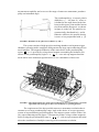
5.0 The System Setup for Module Measurement...................................... 35
5.1 The VXI (VME eXtensions for Instrumentation) System.................................... 37
5.2 The VME-PCI8000 interface................................................................................ 40
5.3 VME ..................................................................................................................... 41
5.4 The VME modules................................................................................................ 42
5.4.1 The BC96 Bias Card...........................................................................................................46
6.0 Hybrid Evaluation ............................................................................................... 51
6.1
6.2
6.3
6.4
Introduction .......................................................................................................... 51
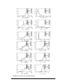
The Chip Configurations ...................................................................................... 52
Results .................................................................................................................. 53
Conclusions .......................................................................................................... 59
7.0 Offline Analysis of Test-Data from an SCT128B readout chip .. 61
7.1
7.2
7.3
7.4
7.5
7.6
The Threshold Scan .............................................................................................. 61
The Basic Front-End Parameters: Gain, Offset and Noise ................................... 62
Results .................................................................................................................. 66
Sources of possible misinterpretations due to the test procedure......................... 71
Evaluation ............................................................................................................. 73
Conclusion ............................................................................................................ 76
8.0 Testbeam ................................................................................................................. 77
8.1 Motivation............................................................................................................. 77
8.2 The 1997 H8 setup................................................................................................ 79
8.3 The H8 DAQ......................................................................................................... 80
8.3.1 The Read-out Control Board ..............................................................................................81
8.3.2 The TDC.............................................................................................................................82
8.4 The Trigger Logic................................................................................................. 83
8.5 Conclusions .......................................................................................................... 84
9.0 Conclusions........................................................................................................... 85
Appendix A............................................................................................................. 87
Introduction
The purpose with a particle physics experiment is always to find answers to fundamental questions about nature. CERN is a center where such experiments are executed. The work described in this thesis is done as part of the research and development
performed by the SCT group in the ATLAS collaboration at CERN.
The focus of the project has been on the binary readout electronics of the SCT
detector modules and the testing of these. Prior to allowing these electronics to be put
in a physics experiment, they need extensive testing, and a lot of design parameters
need to be optimized.
The purpose of this thesis is to
1. Describe my work with the setup of a DAQ system for evaluation of binary
Front-End electronics designed for the ATLAS SCT. This is done in chapters
5.0 and 6.0.
2. Present a way of analysing test-data acquired with a DAQ system similar to the
one set up in Oslo and to present an evaluation of the results of these tests. This
presentation is given in chapter 7.0.
3. Give a short description of my work in the H8 test-beam area at CERN. This
description is found in chapter 8.0.
To fully understand this thesis however, it is necessary to put it in a context.The
following chapters will therefore give a brief introduction to CERN and LHC
(chapter 1.0) and a more detailed description of the ATLAS detector (chapter 2.0), its
Inner Detector and the SCT system (chapter 3.0). Then the work with my project, the
evaluations and a conclusion will be presented.
27 May 1999
1
2
27 May 1999
1.0 CERN
CERN, the European Laboratory for Particle Physics is the most important
research centre for experimental particle physics in the world. CERN is a gigantic
accelerator centre for nuclear and particle physics sited right outside Geneva in Switzerland. The most important activity at CERN the last years has been the LEP (Large
Electron-Positron collider), a ring-shaped accelerator with a circumference of 27km.
1.1 LHC
Inside the LEP tunnel a new collider is being built -the LHC (Large Hadron
Collider). A detailed description of the LHC project can be found in [1]. This section
briefly summarizes the most important points. Before the opening of the LHC in 2005,
there are still a lot of technical problems to overcome. These problems arise mainly
from the much stricter requirements to the LHC detectors compared to the LEP detectors. The extremely high collision rates (~20 collision every 25ns) at LHC requires
very fast detectors and readout electronics. This must be achieved without fatal loss in
effectivity(signal/noise ratio). The much higher luminosity requires radiation-hard
detectors. Synchronisation of millions of sensor elements and readout channels will be
very demanding and the data bundling will be extremely complex. In order to reach the
high luminosity required (1034 cm-2 s-1), the LHC uses two counter-rotating beams
made up of 2835 closely spaced bunches of 1.1x10¹¹ particles each.
The luminosity, L, is defined as in the equation below where ‘f’ denotes the collision frequency, ‘N1’ and ‘N2’ denote the number of particles in each bunch and
A=4 πσ 1 σ 2 is the beam cross sections at the collision point.[2]:
N1N2
L = f -------------A
The LHC will consist of two “colliding” synchrotrons installed in the 27 km
LEP tunnel. They will be filled with protons delivered from the SPS and its pre-accelerators at 0.45 TeV. Two superconducting magnetic channels will accelerate the protons to 7-on-7 TeV, after which the beams will counter-rotate for several hours,
colliding at the experiments until they become so degraded that the machine will have
to be emptied and refilled.
The basic layout of the accelerator features eight straight sections each approximately 528 m long, available for experimental insertions or utilities. The two highluminosity insertions are located at diametrically opposite straight sections, point 1
(ATLAS -A Toroidal LHC ApparatuS) and point 5 (CMS -Compact Muon Solenoid).
Two more experimental insertions are located at point 2 (ALICE -A Large Ion Collider
Experiment) and point 8 (LHC-B (B physics)). This layout is shown in figure 1. These
latter straight sections also contain the injection systems. The beams cross from one
ring to the other only at these four locations. ALICE is a heavy ion colliding experiment while both the CMS and ATLAS are proton-proton colliding experiments.
27 May 1999
3
FIGURE 1. Schematic Overview of the LHC Accelerator
LHC is, as mentioned, a synchrotron and therefore a three-step accelerating
machine.
•An alternating electrical field of RF frequency 400MHz boosts particle
bunches with 25ns spacing -that is: Every tenth RF bucket is filled.
•Dipole magnets of 8.36T bends the tracks. Superconductivity makes this possible. This is the ability of certain materials, usually at very low temperatures, to
conduct electric current without resistance and power losses, and therefore produce high magnetic fields. For comparable power consumption, the LHC can
delivery 25 times the energy and 10,000 times the luminosity of the SPS collider.
•Quadropole magnets (and other multipole magnets) are used to collimate the
beam. To achieve a high luminosity, the point is to keep the bunch of particles as
focused as possible, the cross section of the bunch as small as possible.
In order to achieve the desired magnetic field-strengths, the magnets need to be
operated at a temperature as low as 1.9K. In all, LHC cryogenics will need to cool
down 31 000 tons of material and the total inventory of liquid helium will be 700 000
litres.
4
27 May 1999
FIGURE 2. Cross Section of LHC Tunnel
The LHC will be able to operate at energies in the neighbourhood of 14 TeV for
proton-proton collisions and 1250TeV for heavy ion collisions, which is completely
unknown territory. The LHC is of course designed to search for phenomena predicted
by current models, but since the energies are so high, one must be as prepared as possible for surprises.
1.2 The Standard Model
The mathematical model modern particle physics is based upon is the so-called
Standard Model. The main idea here is that there are 3 families of fundamental particles:
1. Quarks.
There are 6 different quarks: u(p), d(own), s(trange), c(harm), b(ottom) and
t(op). They can only exist in a composition with other quarks (because of their
colour charge), and have electrical charge -1/3 or +2/3. These are the constituents of all hadrons, -with 3 quarks in baryons and a quark and an antiquark in
mesons.
2. Leptons.
There are 6 of these too -3 negatively charged (electron, muon and tau) and 3
neutral ones(neutrinos). These exist independently and are, as far as we know,
point particles -that is: We have not yet seen any signs of size or structure for
these particles.
3. Force-carrying particles.
The 4 fundamental(?) forces each have their force-carrying particles. The
strong force is carried by the massless gluon, the electromagnetic force has the
photon and the weak force has the massive W and Z particles. The theory of
gravitation is not implemented in the Standard Model (or any other quantum
mechanical model) and any ‘graviton’ has, in fact, never been observed.
27 May 1999
5
4. Antiparticles
In addition to the former, there is an antiparticle for each particle in the Standard Model. An antiparticle has exactly the same mass as its “original” and
opposite quantum numbers.
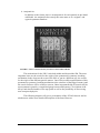
FIGURE 3. Chart of the Elementary Particles in the Standard Model
The motivations for the LHC reach both within and beyond the SM. The most
important issue are the search for the origin of the spontaneous symmetry-breaking
mechanism in the electroweak sector of the SM -or, put in a different way, the search
for the origin of the different particle masses. One of the possible manifestations of this
spontaneous symmetry-breaking mechanism is the existence of the Higgs-boson(s) and
the search for these will be of major concern. Other important fields of research will be
supersymmetric particles, composited gauge bosons and leptons, CP-violations in Bdecays and detailed studies of the top-quark as well as the possibility of discovering
new unexpected physics.
The following chapters will give a presentation of the ATLAS detector and its
subdetectors with a more detailed description of the Inner Detector.
6
27 May 1999
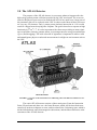
2.0 The ATLAS Detector
The purpose of the ATLAS detector is to measure whatever happens after the
high energy proton-proton collisions provided by the LHC accelerator. The cross-sections for the physics processes to be studied with ATLAS are small over a large part of
the parameter space to be explored at the LHC. In other words: Most of these processes
are very rare. For instance: Only 1 proton-proton inelastic interaction in ~10 13 would
result in a Higgs boson decaying into 4 leptons. The goal is therefore to operate at high
luminosity(1034cm-2 s-1). It is also important with a detector providing as many signatures as possible (electron, gamma, muon, jet, missing transverse energy measurements
(Etmiss) and b-tagging). The wide selection of signatures is important to achieve solid
and unambiguous physics results and measurements in a high rate environment such as
the LHC.
FIGURE 4. Overview of the ATLAS detector indicating where the different subdetectors are
located.
The entire ATLAS detector consists of three main parts; From the Interaction
Point (IP) and outwards these are: -the Inner Detector, which will be described more
extensively in the two chapters to come, and its solenoid, the Calorimetry part, which is
divided into hadronic and electromagnetic subsections, and the Muon Detectors at the
outermost of the ATLAS detector.
27 May 1999
7
2.1 The Muon Detector
The only particle, in addition to the neutrino, that is not completely stopped by
the calorimeters is the muon1. The muon is a Lepton with a mass 200 times the electron
mass and has no hadronic interaction. Since the cross section for bremsstrahlung,
which is the dominating type of energy loss at this part of the energy scale, is inversely
proportional to the square of the particle mass, the bremsstrahlung cross section for the
muon compared to the electron is reduced by a factor of 40.000. In other words, the
probability for stopping the muon with the calorimeter is vanishingly small. To exploit
the physics signature potential of high momentum final state muons, an additional
tracker in a magnetic field is built outside the calorimeters, namely the muon detector.
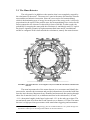
FIGURE 5. The muon detector are arranged in 3 layers around the calorimeters and the inner
detector.
The most important role of the muon detector is to reconstruct and identify the
muon tracks, measure their momenta and provide information to be matched with data
from the inner detector. Muon tracks are identified and measured after passing through
about 2m of material (lead, LAr, scintillators and Iron in the calorimeters) -in total
~11 λ (absorption lengths) in the barrel region and ~12 λ in the end-cap sections. The
measurements start at 5m from the IP and extends over a distance of 5-10m. The muon
detector is a high precision spectrometer with stand-alone triggering and momentum
1. This is not completely true since high energy particles of different flavours can “punch through” the
calorimeters and be part of the background radiation in the muon detector.
8
27 May 1999
measurement capability and covers a wide range of transverse momentum, pseudorapidity and azimuthal angle.
The pseudorapidity, η , at a space point is
defined as η = – ln ( tan θ ⁄ 2 ) , where θ
is defined as the angle between the line
between this space point and the Interaction Point and the beam axis -as shown
in figure 6 on the left. The particles are
symmetrically distributed in φ , and in
hadronic collisions, the particle density
is more or less proportional with η . [1]
FIGURE 6. Definition of the spherical coordinates
φ and θ .
The system consists of high precision tracking chambers and separate trigger
chambers operating inside a magnetic field generated by large superconducting air-core
toroid magnets. The magnetic deflection of the muon tracks in the pseudorapidity
region η ≤ 1.0 is provided by a large barrel magnet surrounding the hadronic calorimeter. In the pseudorapidity region 1.4 ≤ η ≤ 2.7 two end-cap magnets bend the
tracks while in the transition region between, it is a combination of these two.
FIGURE 7. Three-dimensional view of the superconducting air-core toroid magnet system. The
right-hand end-cap magnet is shown retracted from its operating position.
The requirement of the best possible transverse momentum resolution that is
constant over a large pseudorapidity range, leads to the choice of an open-geometry
system of superconducting toroidal magnets. The magnet system consists of three aircore superconducting toroids (figure 7) designed to produce a large volume magnetic
field covering the pseudorapidity range 0 ≤ η ≤ 2.7 , with an open structure that minimizes the contribution of multiple scattering to the momentum resolution.
27 May 1999
9
2.1.1 The Precision Chambers
The momentum of a charged particle can be determined from its deflection in a
magnetic field. To be more precise it is proportional to the radius of the curvature of the
track. The track is measured in 3 stations and in each station several layers of detectors
measure the position and direction of the track.
Two different techniques are used to acquire the high precision track coordinate
measurements. The Monitored Drift Tubes (MDT’s) are used over most of the pseudorapidity range while close to the interaction point and at large pseudorapidities the Cathode Strip Chambers are used due to their higher granularity. This makes the CSC’s
more suitable to cope with the demanding rate and background conditions. In the barrel
region the chambers are arranged in 3 cylindrical layers around the beam axis while in
the end-cap and transition regions the chambers are aligned vertically -also in 3 layers,
or ‘stations’. Each MDT detector plane is made of 2 multilayers of pressurized Al drift
tubes while the CSC’s are multiwire proportional chambers.
2.1.2 The Trigger Chambers
A Level1 muon trigger is (a rough muon pT-measurement) derived from 3 trigger stations. Each station is made of 2 (3 in the TGC’s) planes of strips (or wires) with
X and Y read out. The trigger is based on a coincidence between a strip (or a wire) hit
in the 1st station and a range of strips(wires) in the 2nd and 3rd station. The trigger
chambers are also responsible for bunch-crossing identification.
The trigger chambers use Resistive Plate Chambers (RPC’s) in the barrel region
and Thin Gap Chambers (TGC’s) in the end-cap region and together they cover the
region η ≤ 2.4 . The trigger chambers also provide a second-coordinate measurement
of the track position along an axis parallel to the MDT wires and in a direction parallel
to the magnetic field lines. The trigger chambers are fast, but have a coarse spatial resolution. The RPC’s are gaseous, parallel-plate detectors while the TGC’s are multiwire
proportional chambers.
10
27 May 1999
FIGURE 8. Overview of the muon system, indicating where the different chamber technologies
are used.
2.1.3 Performance/Physics Requirements
When designing a detector, there must exist a set of rough guidelines for the different requirements for the detector -a general idea of how it should work and what it
should discover. For the muon detector, these can be summarized as follows:
•Like the rest of the LHC, the muon detector must feature the largest possible
discovery range of both expected and unexpected physics.
•It must provide a good discrimination against difficult background conditions.
•Stable operation during the anticipated lifetime of the LHC is required.
Although ATLAS is a general purpose pp detector, it is impossible to be equally
sensitive to all the possible varieties of new physics. The discovery potential of the
muon detector is therefore optimized with certain benchmark processes in mind:
•Standard model and supersymmetric Higgs decays (i.e. H → Z Z ∗ → 4l and
H → Z Z → 4l ).
•New vector bosons (i.e. Z ′ → µµ and W ′ → υ µ µ ).
•Semileptonic b- and t-decays (i.e. b → µx )
•CP-violating processes
The full description of the ATLAS Muon Spectrometer can be found in [3].
This section summarizes the basic concepts.
27 May 1999
11
2.2 The Calorimeters
A calorimeter is a composite detector using total absorption of particles to
measure the energy and position of incident particles or jets. In the process of absorption, showers are generated by cascades of interactions (bremsstrahlung and pairproduction). Characteristic interactions with matter (e.g. atomic excitation, ionization) are
used to generate a detectable effect, via particle charges. The result of a series of statistical processes is more predictable when the number of processes are large. The basic
phenomena in showers are statistical processes, hence the intrinsic limiting accuracy,
expressed as a fraction of total energy, improves with increasing energy as [4]:
∆E
1
------- ∝ ------E
E
The calorimeters will play an essential role in ATLAS and at the rest of the
LHC. Since they have the advantage of improved relative resolution with increasing
energy (in contrast to magnetic spectrometers), the LHC energy scale makes the calorimeters very powerful and suitable detectors. The ability of detecting Higgs bosons
depends heavily on the calorimeter performances. Most decay modes have final states
that will be reconstructed mainly in the calorimeters.
FIGURE 9. Overview of the ATLAS Calorimetry
12
27 May 1999
The LHC parameters such as the large center-of-mass energy and the high luminosity requires good detector performance in an unprecedented part of the energy
scale. ATLAS must also feature the ability to deal with the pile-up effect due to the
high rate and particle fluxes, and minimise the effect such a pile-up could have on the
physics performance. Extreme radiation resistance capabilities are also required
because of the 10 year (at least) operation time in this hostile environment.
The calorimetry is divided in two main parts: The electromagnetic and the
hadronic calorimeter. The EM calorimeter is mainly sensitive to electrons and photons
through bremsstrahlung and pair-production which dominate at high energy, while the
hadronic calorimeter is sensitive to hadrons.
The main tasks of the ATLAS calorimetry are:
•accurate measurements of the energy and position of electrons and photons
(EM calorimeter)
•measurement of the energy and direction of jets (Hadronic calorimeter)
•measurement of the missing transverse energy of the event (EM + Hadronic
calorimeter)
•particle identification (i.e. separation of electrons and photons from hadrons
and jets and separation of τ hadronic decays from jets)
•event selection at the trigger level.
2.2.1 The Electromagnetic Calorimeter
The EM calorimeter consists of a barrel and two end-caps and is a lead-LiquidArgon detector with lead absorber plates and accordion-shaped kapton electrodes. It is
preceded by a presampler detector which task is to correct for the energy loss in the
material upstream of the calorimeters (the inner detector, the cryostats and the coil).
This energy loss is due to bremsstrahlung interactions and the photons created in this
process are absorbed in the presampler. The measured photon energy is then added to
the corresponding particle. This presampler consists of an active LAr layer of 1.1cm in
the barrel section and 0.5cm in the end-cap section.
27 May 1999
13
FIGURE 10. Layout of the EM barrel calorimeter and LAr accordion geometry
The barrel part, which is contained in a barrel cryostat surrounding the inner
detector cavity, consists of two identical half-barrels. The EM end-caps are divided into
two coaxial wheels and are also contained in cryostats together with the end-cap and
forward hadronic calorimeters (See figure 12).
To ensure an acceptable level of high-energy-shower containment the total
thickness of the EM barrel is at least 24 X0 thick and at least 26 X0 thick in the endcaps.
The full description of the ATLAS LAr Calorimeter can be found in [5]. This
section summarizes the basic concepts.
14
27 May 1999
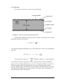
2.2.2 The Hadronic Calorimeter
The hadronic calorimeter consists of three main parts, the barrel, the end-cap
and the forward calorimeter.
FIGURE 11. The plastic scintillating tile.
The barrel part is subdivided in a central barrel
and two extended barrels. The sampling technique
used here uses plastic scintillating plates (or ‘tiles’
-shown in the figure to the left) embedded in an
iron absorber. The tiles are aligned perpendicular
to the beam direction and staggered in depth. To
provide a good hadronic shower containment and
minimize punch-through for the muon system, the
thickness of the calorimeter is an essential parameter. The total thickness of the barrel calorimeter
(EM + tile) at η = 0 is about 9.2 λ (absorption
lengths). This is sufficient to achieve a good resolution on high energy jets. The total amount of
material in front of the muon system is 11 λ including outer support and is enough to
reduce the punch through to an acceptable level.
In the end-caps and the forward calorimeters, where a higher radiation resistance is needed, the more radiation-hard LAr technology (LAr is easily replaced during
operation) is used. The hadronic end-cap calorimeter is a copper-LAr detector with
parallel-plate geometry. It consists of two separate wheels with equal diameter and
together they have ~12 λ active material.
FIGURE 12. A more detailed view of an end-cap cryostat with its content.
27 May 1999
15
The forward calorimeter is a dense (9 λ in a rather short longitudinal space)
LAr detector consisting of regularly spaced longitudinal channels filled with rod electrodes in a metal matrix. It consists of three longitudinal sections. The first one is in
copper, the other two are in tungsten. The sensitive medium, LAr, fills the gap between
the rod and the matrix. The forward calorimeter is also integrated in the end-cap cryostat with its front about 5 meters from the interaction point. Due to the high level of
radiation, this makes it an especially challenging detector. It provides, however significant advantages for the forward jet tagging and the Etmiss measurements.
The full description of the ATLAS Tile Calorimeter can be found in [6]. This
section summarizes the basic concepts.
16
27 May 1999
3.0 The Inner Detector
The ATLAS inner Detector covers the pseudorapidity region η < 2.5 and is
composed by 3 main parts, the TRT (Transition Radiation Tracker), the Pixel detector
and the SCT (SemiConductor Tracker).
FIGURE 13. The Inner Detector Geometry
The main purposes with the ID are pattern recognition and track reconstruction,
but momentum measurements, electron identification and tagging of b-jets are also
important issues. Another important requirement, besides the performance requirements, is to minimize the amount of material in the Inner Detector. This is crucial
because of the deterioration of the calorimeter resolution according to an increase in
the amount of material preceding the calorimeters. This yields detectors, electronics,
cooling system, cables and support structure, in short: anything that causes radiation to
loose energy.
3.1 The Pixel detector
The Pixel detectors are placed closest to the beam, are aligned in barrels and
disks of modules. The Pixel system provides 3 space points over the whole acceptance
of the Inner Detector. Each module is a semiconductor detector with pixels instead of
microstrips. That is, the strips are divided into much shorter strips (pixels). Each pixel
measures 300x50 µm . There are 140 million pixels distributed over 3 barrels and 8
disks. With the given pixel detector design, this gives a total sensitive area of 2.3 m2.
To be sure not to miss any information, the sensitive area of each module slightly overlaps the neighbouring module.
27 May 1999
17
FIGURE 14. Layout of the Pixel Detector
The pixel detectors provide 2-dimensional spatial information about where a
particle passes through the detector. In order to read out every pixel, the binary readout
electronics have to be mounted on top of the detector. From there the electronics are
connected to each pixel using a bump bonding technique. The innermost layer will be
placed as close as possible to the interaction point to achieve an optimal impact parameter resolution. These detectors are, in addition, much more radiation hard than microstrip detectors and can therefore be placed where the density of particles is highest.
They work both as vertex- and tracking-devices.
The parameters and the layout of the pixel detector are determined by the performance requirements and the desired lifetime of each part of the system. These can
be summarized as follows:
•excellent pattern recognition in high multiplicity environment
•excellent transverse impact parameter resolution and 3D-vertexing capability
•excellent b-tagging and b-triggering capabilities
•lifetimes of about 3 years at reduced LHC luminosity (1033 cm-2s-1), and 1
year at design luminosity (1034 cm-2s-1) for the innermost barrel (the B-layer)
•lifetimes of about 7 years at design luminosity for the rest of the pixel detector
18
27 May 1999
3.2 The TRT
The TRT surrounds the pixel- and SCT-system and are aligned both parallel and
perpendicular to the beam-direction. It consists of layers of straw-detectors where each
straw is a cylindrical, gaseous drift-chamber with a diameter of 4mm. The TRT is
designed as 1 barrel with 52 544 axial straws of about 150cm length and 2 end-cap
parts with 319 488 radial straws of 39-55cm length. The intrinsic radiation hardness
and the low cost compared to other large volume tracking solutions, made this combined straw tracking and transition radiation detecting system very practical. The price
to pay for these advantages is, however, a high detector occupancy with the 370 000
straws and the 420 000 electronic channels.
FIGURE 15. Layout of the TRT Detector
This system provides almost continuous tracking at large radii in the Inner
Detector due to its many measurement points (each particle hits, on the average, about
36 straws. This makes the TRT a powerful tool for pattern-recognition. The performance requirements can be summarized like this:
•tracking
•detection of transition radiation
•good ability to trigger high p T muons at Level2
•together with the EM calorimeter, contribute to the electron identification
•momentum measurements (precise measurements in the R- φ plane)
27 May 1999
19
To obtain this performance, the analogue front-end readout electronics operates
with 2 thresholds; One low, about 200ev, for detecting MIPs (Minimum Ionizing Particles) and one high, 6-7keV, for detecting transition radiation photons (X-rays).
3.3 SCT
The SCT consists of Silicon microstrip detectors. These detectors have successfully been used as tracking devices the past years, but due to the hostile conditions at
LHC at full luminosity (1034 cm-2s-1), challenges connected to radiation damage, scale
and readout procedures arises. I will concentrate only on the readout procedures and
general performance here.
3.3.1 General Description
The SCT modules are aligned in 4 cylindrical, central barrels and 9 forward and
9 backward disks with a total sensitive area of ~50m2.
FIGURE 16. Structure of the SCT Barrel Section
Silicon is, because of its fast signal speed and excellent spatial segmentation,
used as the detector material here, but there are a lot of other considerations for a wellworking detector system than just the properties of the detector medium and the basic
detector units. A lot of practical problems must also be taken into account:
20
27 May 1999
•The expected lifetime of the SCT is 10 years at full luminosity, and during that
time one cannot expect to have too much access to the inner detector. Therefore
we must minimise the need for maintenance and repair and hence make the
design as reliable as possible.
•The Silicon detectors, the front-end electronics, the hybrids and the cables
must be cooled with a specially designed cooling system using binary ice. This
is to minimize the leakage current and the effects of radiation induced doping
changes and to remove heat generated by front-end chips and DC voltage drops.
•The thermal expansion of the material in the support structures must be as
small as possible to ensure the exact locations of the modules. The temperature
variations can be up to 30 ° C.
3.3.2 Modules
A module consists of 2 pairs of daisy-chained detectors -each with an active
area of 61.6x62.0 mm2. 1 pair is aligned on each side of the module with the back side
detectors rotated by 40mrad to the frontside strips which are parallel to the beam direction. The rotation is due to the requirement to provide z-measurement capability. So
why not align the strips orthogonally? Any particularly good resolution in the z-measurement is not needed because the magnet bends the particle trajectory in the r – ϕ
plane. With the backside detector rotated by 40mrad, it also provides an extra r – ϕ
measurement.
When operating in a 2 Tesla magnetic field, as is the case at LHC, the particles
trajectories are diverted according to the Lorentz-force. This causes a signal-spread in
the detector due to the angle the particle hits the detector with. To minimise this effect,
the modules are mounted on the support structure with a tilt angle of 10deg to the tangent. The modules are slightly overlapping each other to minimise loss of information,
or dead areas in the system. The optimal operating temperature of the Silicon detectors,
under these radiation conditions, is -7 ° C.
This temperature is a compromise between annealing and anti-annealing
effects. Highly energetic particles cause bulk damage in silicon by displacing atoms
from the lattice, causing a change in dopant concentration. A change in the full depletion voltage (Vfd) and the leakage current is observed. The time dependence of V fd can
be separated into a short and long term period. The short term annealing is believed to
be dominated by the recombination of radiation induced acceptor sites into inactive
ones and is characterized by a decrease in Vfd referred to as beneficial annealing. A
high temperature is an advantage for this process. At longer time scales Vfd increases
due to the transformation of defects into active acceptor sites, described as the anti
annealing period. A low temperature is preferred to slow down this process. A more
detailed study on the subject can be found in [7]. This section summarizes some of the
basic points.
Within the barrels all modules are identical, but in the disks the modules require
a wedge-like shape, which will not be discussed here.
27 May 1999
21
3.3.3 Detectors
The detector consists of p+ strips on n-type substrate.
FIGURE 17. Layout of a p-in-n-type Si microstrip detector
With a binary readout of the detector, the resolution is a function of the readout
pitch and is given by the variance
2
σ =
∫ f ( x)( x – x)
2
dx
of a uniform probability distribution, f(x), with width ‘Pitch’ where f(x) is normalized
such that
∞
∫
–∞
f ( x ) dx = 1
⇒
1
f ( x ) = -----------Pitch
Pitch
This results in a variance σ = ------------ . Taking the variance, σ , as the resolution
12
of the detector, and given the pitch of 80 µm and the binary readout of individual
strips, we have a point resolution in φ of <23 µm . The sign “less than” is used since a
small percentage of the traversing particles, the ones traversing near the border
between adjacent strips, will cause two strips to register a hit. This improves the resolution since the possibility that one particle causes two strips to fire, is equivalent to a
finer partitioning of the readout pitch.
22
27 May 1999
Heavy particle irradiation is a major problem with these detectors in the LHC
environment. The effects of such irradiation can be summarised as:
•An increase in leakage current will occur due to the structural damages (i.e.
bulk-damage) caused by the heavy particles.
•There will also be a change in the effective doping which, in turn, implies a
change in the necessary voltage to keep the detector fully depleted.After some
time, though, the detector goes through a type inversion. The n-type Si-crystal
will actually have turned into p-type Si-crystal and the pn-junction will have
moved from one side of the detector to the other (see figure 17).
•Due to an increasing amount of impurities and structural damage, effects like
trapping come into play. This causes a decrease in charge collection efficiency
because some of the charge carriers get trapped by these impurities.
After 10 years at full luminosity at LHC we will have type inversion for all sensors and depletion voltages up to 350V. The p-n junction will then be on the n-side of
the detector. It is therefore important to always operate the detectors overdepleted since
a partially depleted detector will have the un-depleted zone on the p-side of the detector. The charge collection then becomes difficult since there is no electrical field near
the strips.
3.3.4 Hybrid
The hybrid is a ceramic piece which carries 6 128-channel chips(SCT128B) and
is glued directly on top of the detector. There will be 2 hybrids on each module -one on
each side. It plays an important part in mechanical support, cooling (transport of heat
away from the chips) and readout. Beryllia (BeO) is chosen as the material for the
hybrid because of its good thermal conductivity and long radiation length (144mm).
There is also an electric circuitry on the hybrid and this performs the following tasks:
•Distribution of power and ground to the Front-end chips
•Distribution of clock and control to the binary pipeline circuitry
•Return of data to the off module optical transmission board
•Filtering and AC current return of the detector bias line
•Support of redundancy functions of digital chips, bypass lines for chip failures
3.3.5 Electronics
Apart from the readout electronics, which I will focus on here, there are a lot of
other features of the SCT which must be put in the rather vague category “Electronics”.
The main tasks of these electronics can be summarized as follows:
•Control the operation of the SCT.
•Provide power for the electronics and the detector bias.
•Provide means for calibration and monitoring (detecting problems with the
SCT before severe damage is done to the system) of all aspects of the SCT operation. This is necessary due to the inaccessibility of the system.
27 May 1999
23
The readout electronics use a binary readout strategy. This means that instead of
reading out the whole shape of the signal collected by a strip, a discriminator fires a hit/
no hit signal depending on the amount of charge collected by the strip. A hit is registered when the amount of charge collected exceeds a certain, preset value. The output
is then stored in a pipeline until a trigger initiates a readout for that particular event.
FIGURE 18. Figure of the Front-end Electronics logic
Front-End (FE) electronics are the electronics between the detector and the Readout Driver and has the following different functional components[8]:
•FE analogue or analogue-digital processing
•LVL1 buffer in which information (analogue/digital) is stored and is retained
long enough to accommodate the LVL1 trigger latency.
•Derandomizer in which the data corresponding to a LVL1 trigger accept are
stored before being sent to the next level.
To obtain a low noise performance, the FE electronics must be mounted directly
on the silicon strip electrodes. This means that these electronics must be in the active
volume of the detector which in turn sets a constraint to the mass and power consumption of the FE electronics. Another requirement for maintaining a stable and satisfying
operation is that noise, pick-up, discriminator-performance and threshold are well controlled.
One of the most challenging aspects of the SCT-design is the compromise
between optimizing performance parameters (noise, efficiency, bandwidth, reliability)
and minimizing power consumption, amount of material and cost.
The full description of the ATLAS detector can be found in [9]. This chapter is
a summary of the most important points.
24
27 May 1999
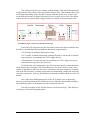
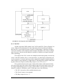
4.0 Read-Out Electronics
Up until now I have given a quite general description of the ATLAS detector.
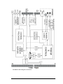
From now on this thesis will present a more detailed description of one specific solution of the readout electronics. This solution is outlined in figure 19.
4.1 The HAC (Header-Adder Chip)
A comprehensive presentation of the HAC is found in [10]. This section summarizes the most important points.
4.1.1 Architecture
The HAC is the local cable interface and readout sequence manager for the readout chips on a hybrid. It is designed to receive control signals from a fibre-optic
header, electrically buffer and decode these control signals and trigger readout
sequences from a bank of chips. In our case this will be the SCT128B chip which facilitates both the preamplifier-shaper-discriminator circuitry and the binary pipeline in
one unit. However, since the HAC was originally designed only to serve the pipeline
part (CDP128) of the older readout system where the pipeline was separated from the
rest, this causes a few non-fatal incompatibilities between the HAC and the SCT128B.
The chip controls and buffers the bit stream from the readout-chips, adds a header with
start code and trigger count, detects certain error conditions (timeout, overflow, underflow) and drives the data line to the fibre-optic header.
FIGURE 19. Block Diagram of Readout System
27 May 1999
25
The signals listed below are involved in the fibre-optic header-to-HAC connection. These signals pass through the fibre-optic link.
Cable Side Signals
CCLK[+/-]
Cable-side Clock (from DAQ)
CTC[+/-]
Cable-side Trigger-Control Signal (from DAQ)
CDV[+/-]
Cable-side Data Signal, voltage signals (to DAQ)
CDI[+/-]
Cable-side Data Signal, current signals (to DAQ)
CRS[+/-]
Cable-side Read-Strobe (optional, from DAQ)
•The clock (CCLK) is a pulse train with approximately 50% duty cycle and frequency range from 100kHz to 60 MHz. The design clock frequency for the electronics are, as mentioned earlier, 40 MHz.
•The trigger/control signal (CTC) is used by the DAQ to program both the HAC
and the readout chips, command certain actions such as calibration or status
dump and the logical trigger signal of the physics experiment.
•The data signal (CDV in our case) carries information (header and hit-pattern)
from the HAC (and the readout chips) to the DAQ.
•The cable-side read-strobe (CRS) is the path which the DAQ can drive a readstrobe to the readout chips. This is an unused feature in our specific setup.
•The HAC output line is provided with both current-mode (CDI -for low input
impedance receivers) and voltage-mode (CDV -for conventional receivers) signals.
The signals listed below are used for communication between the HAC and the
readout chips. These are the hybrid-side versions of the fibre signals and one test configuration signal for the readout chips. Originally (for use with the CDP128) there were
an additional five test and configuration signals, but these are not used with the
SCT128B.
Hybrid Side Signals
HCLK[+/-}
Hybrid Side Clock (from HAC)
HTC[+/-}
Hybrid Side Trigger-Control Signal (from HAC)
HD[+/-}
Hybrid Side Data Signal (from the Readout chips)
HRS[+/-}
Hybrid Side Read-Strobe (from HAC)
TEN
Test-mode Enable Signal (from HAC)
4.1.2 Registers and Logic
The HAC Status Register consists of 48 bits where 32 are writeable and 16 are
read-only. It includes the state of all counters, error flags and programmable registers
on the chip. Executing a Clear instruction will set all the bits of the status register to
zero. The Status Register contains the following fields:
26
27 May 1999
HAC Status Register
DV[5:0]
Input to programmable voltage source
writeable
DI[5:0]
Input to programmable current source
writeable
RSA[1:0]
Read-Strobe Algorithm selection register
writeable
HPR[8:0]
Header Pattern Register
writeable
TD[3:0]
Test-mode Data Register
writeable
TEN
Test-mode Enable
read-only
EEN
Edge-mode Enable
read-only
TOF
Time-Out Error Flag
read-only
OFF
Read-Out Buffer Overflow Flag
writeable
UFF
Read-Out Buffer Underflow Flag
writeable
RS[3:0]
Read-Strobe Counter
read-only
CC[1]
Compliment Hybrid-Clock Control Bit
writeable
CC[0]
Compliment Latch-Clock Control Bit
writeable
CT
Clock-Through Control Bit
writeable
BOR[8:0]
Buffer Occupancy Register
read-only
When writing to the status register, 32 bits must be supplied via the CTC signal
following the Write-Status command. When reading from it, 48 bits will be asserted
serially on the CDV signal in response to the Read-Status command.
The read-strobe signal is produced according to one of three algorithms: an
externally supplied RS (RSA[1:0]=0), an RS generated from command to HAC
(RSA[1:0]=1) and a locally generated RS (RSA[1:0]=2). The option in use in our setup
is RSA=1 -an RS generated from command to HAC.
To decide the read-strobe condition, the HAC uses a string of 9 flip-flops called
the Buffer-Occupancy Register (BOR). This register keeps track of the SCT128B readout buffer. For every trigger received, one flop is set and for every read-strobe, one flop
is cleared. If all flip-flops become set and an additional trigger arrives, the OverFlow
Flag (OFF) is asserted. This indicates that data has been overwritten in the SCT128B’s
9-event read-out buffer. If none are set and a read-strobe occurs, the UnderFlow Flag
(UFF) is asserted. This indicates that an unwritten buffer location is being read from.
The HAC also detects the time-out condition by using a 10-bit time-out counter.
This counter starts counting from 0 when FIRST is asserted, and if it reaches 1024
clock cycles before the END signal arrives at the HAC, the Time-Out Flag in the HAC
status register is set and FIRST is lowered.
The CC1 and CC0 status bits allow adjustment of relative timing between clock/
data and clock/hybrid-side control signals respectively. The CC1 bit allows adjustment
of the relative phases of the hybrid clock and hybrid control signals and the CC0 controls which edge of the clock cycle data is latched into the HAC from the hybrid. The
CT status bit is used to put the HAC into ‘Clock-Through’ mode. This means that if
this bit is set, the HAC drives the clock as received back out the CD line.
27 May 1999
27
Commands.
The HAC decodes four commands from the CTC line. These are initiated by
sending the sequences listed below through the CTC line.
•The Clear command clears the state of all counters, error flags and readoutchip bus control signals (RS and FIRST) to zero.
•In response to a Read-Status command, the HAC shifts out the state of its 48bit status register onto the CD line.
•In response to a Write-Status command, the HAC shifts the next 32 values on
the CTC line into the writeable parts of its status register.
•The Read-Strobe command causes the HAC to send a read-strobe pulse to the
readout chips.
HAC Commands
x11110000x
Clear State of HAC
x11110001x
Read HAC Status Register
x11110010x
Write HAC Status Register
x11111100x
Generate Read-Strobe
As will be clarified later these commands may also have a side-effect of triggering some instructions to the SCT128B’s.
4.1.3 Readout
A successful readout of an event from the hybrid, requires a specific series of
events:
5. A pending trigger
6. The readout chips receive a Read-Strobe pulse
7. FIRST[+/-] signal (LAST signal of the first readout chip in the chain) is raised
by HAC
8. The readout chips pass read-out flag via the LAST-NEXT connections
9. The END signal (NEXT signal of the last readout chip in the chain) is raised by
the last readout chip.
The bit-sequence driven down the CD-line by the HAC during readout of an
event will look like this:
•9-bit Header pattern from HPR[8:0]
(HRS pulsed for one clock at this time)
•Time-Out Flag
•Overflow Flag
•Underflow flag
•4-bit read-strobe count
28
27 May 1999
(FIRST asserted by HAC at this time)
•128-bit hit-pattern from each SCT128B
(HAC expects END to become true after the last chip is read out)
FIGURE 20. Logical Events in a Read-out Sequence
Figure 20 shows the logical events in a read-out sequence involving a hybrid
with two SCT128B’s. Readout is initiated by the receipt of a pulse on the CTC line.
This is passed on to the hybrid followed by an HRS read-strobe pulse. When the HAC
has completed transmission of the header (containing start-code and trigger count),
FIRST is asserted, initiating the token chain. The first SCT128B then unloads its 128bit output register onto the HD line and then raises its NEXT signal. This is the token
pass to the second SCT128B in the chain, labelled TOKEN1 in the figure. The second
SCT128B then unloads its output register. When complete, it raises its NEXT signal,
which, since this is the last read-out chip in the chain, also is the END signal of the
token chain. When the HAC senses that END has been asserted, it lowers FIRST, terminating the read-out sequence for the corresponding trigger.
Bug List.
The Time-Out flag is reset at the beginning of each read-out sequence. Because
the Time-Out flag is part of the header, its resultant value for a read-out sequence in
progress is not known until after the header has been sent up the cable. Therefore, the
TOF is always FALSE in a header. Its actual value for a read-out sequence can only be
known by reading the status register after the read-out sequence.
According to [10] there are four dead clocks between the header and the beginning of chip data coming through the CD line. This means that the first four bits from
the read-out chip, will be lost. For the CDP, these were taken from the column code and
did not result in any loss of data. However, for the SCT128B, which does not provide
such a column code, four bits of data will be lost.
FIRST is not lowered for 17 clocks following END. This leads to some waste of
time, but should not cause any loss of data.
27 May 1999
29
The hybrid-side output signals from the HAC are not defined during a write-status-register operation. Stabilizing these signals during this operation would be an
advantage to prevent disruption of the read-out chips during status register writes.
4.2 SCT128B
A comprehensive presentation of the SCT128B is found in [11]. This section
summarizes the most important points.
4.2.1 Architecture
The SCT128B chip is a 128 channel integrated circuit for binary readout of silicon strip detectors for the ATLAS SCT designed for the DMILL technology. The
preamplifier-shaper-discriminator circuitry and the binary pipeline are both implemented in one single chip. To be able to use it in an already existing readout system,
the back-end and control logic are compatible with the architecture of the previous version, CDP128, and the HAC. The block diagram is shown below:
FIGURE 21. Block Diagram of SCT128B
30
27 May 1999
4.2.2 Front-End
The Front-End part comprises 4 main functional blocks:
1. The preamplifier-shaper-discriminator circuitry with the designed processing
parameters:
Signal Processing Parameters
Parameter
Value
Differential gain at the input of discriminator
100 mV/fC
Peaking time
20 ns
Time Walk
15 ns
Double Pulse Resolution
50 ns
Discriminator ‘off’ state output level
4V
Discriminator ‘on’ state output level
0V
2. A calibration circuitry. Each channel has its own internal calibration capacitor
of 100 fF which can be pulsed with signals applied to 1 of 4 external inputs (test
0-3) or with signals delivered from the internal calibration circuitry. During calibration one fourth of the channels are stimulated and tested simultaneously. If
the internal calibration circuitry is used, the calibration line to be activated is
selected by a 2-bit address(cald0,cald1).
Calibration Line Addressing
Cald 0
Cald 1
Pulsed Test Line
Pulsed Front-End Channels
0
0
test 0
ch 0,4,8,...
0
1
test 1
ch 1,5,9,...
1
0
test 2
ch 2,6,10,...
1
1
test 3
ch 3,7,11,...
3. A DAC for the calibration amplitude. The test signal amplitude is set by this 8bit internal DAC and the test signal is triggered by a calibration strobe signal
generated by the Control Logic (following the slow command 10xx). The calibration strobe can be delayed (with respect to clock) within the range of 50 ns
with 5-bits resolution and its duration is fixed and equal to 200 ns.
Calibration Amplitude
Pulse Amplitude
Charge Injected via a 100 fF capacitor
Range
0 - 160 mV
0 - 16 fC
Resolution
0.625 mV/bit
0.0625 fC/bit
4. A DAC for threshold control. The threshold is determined by a differential voltage applied either from external pads(VT1,VT2) or from this internal 8-bit
DAC. These DAC circuits comprise internal voltage references. The range of
the threshold DAC is 640 mV with a resolution of 2.5 mV/bit.
27 May 1999
31
4.2.3 Registers and Logic
Input Register.
The Input Register has 2 functions: -edge sensing of signals delivered from the
discriminators and channel masking. For every hit detected by a discriminator only a
single pulse of duration 1 clock period is provided regardless of the time response from
the discriminator. The channel mask register is used for disabling bad or noisy channels
so that the data from these are not written to the pipeline. To mask a channel one must
set the corresponding bit in the mask register to “1”. In Test mode (selected by the TEN
signal) the mask register can be used to apply test patterns to the pipeline. The mask
register is loaded serially.
Pipeline.
The binary pipeline is designed as a multiplexed FIFO circuit in which an array
of nxn dynamic memory cells are controlled by n non-overlapping clock signals. In
each clock cycle only n cells out of nxn are switched while the effective delay provided
by such a block is equal to nx(n-1) clock cycles. The pipeline has 128 channels with
depths of 132 bits. The hit pattern from the input register is shifted through the pipeline
during 132 clock cycles. When a Level1 trigger arrives, the pattern from the pipeline
output is written to the Readout buffer. The slow command CLEAR resets the clock
generator while the contents of the pipeline remain unchanged.
Readout Buffer.
The Readout buffer is a dual-port static RAM array which is 128 bits wide and 9
words deep. It holds hit patterns corresponding to each L1 trigger during readout
allowed by the readout strobe. There are 2 pointers which address the memory, one for
reading and one for writing, allowing for simultaneous reading and writing. The pointers are cleared by the slow command CLEAR. This buffer serves as a derandomizer
which removes the fluctuations from the L1 trigger distribution.
Output Register.
The Output register is a 128-bit parallel-to-serial shift register. For each L2 trigger, the oldest data from the readout buffer are shifted to the output register and read
out serially.
Control Logic.
The control logic is based on the concept used in the CDP128 and the HAC but
compared to the CDP128, there are a few new functions which I have already mentioned; The DACs for threshold control, calibration amplitude and delay control for the
calibration strobe are all new. Modified software is therefore needed to make use of
these functions. The control logic comprises a 21-bit register:
•8 bits for threshold control DAC
•8 bits for calibration amplitude DAC
•5 bits for calibration strobe delay
32
27 May 1999
4.2.4 Level1 and Control Commands
The L1 trigger commands are summarized in the table below.
L1 trigger commands
x010x
One L1 trigger
x0110x
Two consecutive L1 triggers
x01110x
Three consecutive L1 triggers
For each L1 trigger received, a 128 bit word is read out of the pipeline and written into the readout buffer. The first command is used in normal data taking mode
while the other 2 can be used in test mode or for data taking with cosmic radiation.
If a sequence x01111 is received, the next 4 bits are decoded in the following
manner:
Control Commands
Command
Function
00xx
Clear pointers in the RO buffer and the pipeline
01bb
Load calibration address register with bb
1110
Load the next 21 bits into the DAC & Delay
register (thrDAC + calDAC + cal-pulse delay)
The most significant bit is always shifted first.
1111
Load the next 128 bits into the mask register
(first bit corresponding to channel 127).
After power-up, the state of the different registers in the chip is undefined. The
following sequence of commands should therefore be executed in order to define this
initial state:
1.
L1 trigger + at least 130x0
010 <130x0>
2.
CLEAR
1111 00xx 0
3.
Load DAC &Delay register
1111 1110 <21 bits> 0
4.
Load mask register
1111 1111 <128 bits> 0
The additional ‘0’ after each command is required to ensure correct execution of
the different commands. Commands 3 & 4 were not implemented in the CDP128 and
may have a side-effect to the HAC state. Execution of the CLEAR command for the
HAC is therefore advised after initialization of SCT128B.
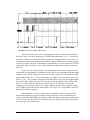
Readout Protocol.
At the arrival of a L2 trigger (readout strobe) the oldest data from the readout
buffer is written to the output register. When a LAST signal is received, 128 bits are
shifted out serially and a NEXT signal is passed on to the next chip in the chain -that
may be another SCT128B or the HAC. The L1 and L2 signals are validated by the rising edge of the clock while the LAST signal is validated by the falling edge. A readout
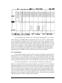
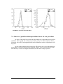
sequence with the test pattern F0F0F0F0.... will look like shown in figures 22 and 23:
27 May 1999
33
FIGURE 22. Close-up of the Start of the Readout Sequence
FIGURE 23. The Complete Sequence
34
27 May 1999
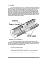
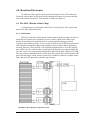
5.0 The System Setup for Module Measurement
This chapter describes the hardware setup for module measurements as used in
both Uppsala and Oslo.
When a particle traverses the silicon detector, a small electric signal is created
and collected by the readout strips. This tiny signal is then routed through the different
parts of the Front-End electronics where it is amplified, discriminated and read out. To
simulate a real experimental situation we simply inject a charge of proper size (on the
order of the charge ionized by a particle traversing a detector) into the calibration
capacitor (100 fF) at the input. The main purpose of this system is to test the electronics with respect to noise and certain features, which will be explained in more detail
below, like ‘gain’ and ‘offset’.
What is important to know about a chip before it is bonded to a detector and put
in an experiment? And what requirements to functionality is set? Prior to this discussion it is necessary to define some key concepts:
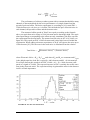
Threshold: When a signal is being discriminated, what happens is that a comparator compares the amplitude of the amplified pulse with a certain fixed referencevalue. If this amplitude exceeds the reference, the signal is defined as a hit and given
the binary value ’1’ which will be the only information about the signal to be stored in
the digital pipeline and read out. If it does not exceed this value, a ‘0’ is written to the
pipeline which, of course, means that no particle traversed the strip corresponding to
the channel being read out. This fixed value in the comparator is called the “Threshold”.
Gain: The charges generated in the silicon detector are very small. To be able to
discriminate them with some accuracy they are, after being driven through a calibration
capacitor of 100 fF, amplified before they are discriminated and read out. The “Gain” is
a measure on the size of the voltage generated in the chip as a function of injection
charge. How this parameter is calculated, will be explained in chapter 7.0.
Offset: Every channel has an ‘intrinsic’ DC voltage level which, in general, is
different from channel to channel and is due to the processing of the chip. Reading out
an analogue signal of a channel (if it was possible) without any charge injected into the
input would result in a signal with signalheight equal to the offset.
Efficiency: The percentage of channels that gave triggers during a read-out
sequence is defined as the “Efficiency”.
Noise Occupancy: There will always be a certain level of noise on the inputs of
the chip. This noise can also result in triggers if the amplitude of this noise exceeds the
threshold level. The percentage of channels that, averaged over a long time, are defined
as hit because of noise-triggers, is called “Noise Occupancy”.
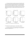
With these definitions in mind, it is possible to form a list of requirements to
chip performance and functionality:
27 May 1999
35
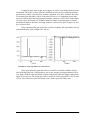
•The possibility to fix a threshold such that, with an injection charge corresponding to about 1 MIP (Minimum Ionizing Particle), the noise occupancy
–4
does not exceed 5 ×10
and efficiency does not drop below 99%.
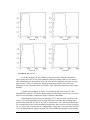
FIGURE 24. Sketch illustrating the above requirement
•The channel-to-channel gain-spread should be minimized -this to keep the
response from the channels as uniform as possible. Identical signals should be
amplified and discriminated equally from one channel to another.
•The threshold spread should be minimized. If the threshold is set to 100mV,
the actual threshold in the chip should not be too far away from this value. The
largest factor contributing to the threshold spread is, however, the spread in offsets. 1mV difference from one channel to another in the offset means 1 mV difference in the actual threshold.
•The percentage of bad channels on one chip/module must be minimized.
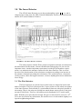
The complete setup of the test-system will look as illustrated in figure 25. The
details of each component will be explained throughout the rest of this chapter.
36
27 May 1999
FIGURE 25. The Oslo lab-setup.
5.1 The VXI (VME eXtensions for Instrumentation) System
The compatible platforms for the National Instruments VXI-system is NI
embedded controllers and external computers with an MXIbus interface.
VXIbus:
VXI is a superset of VME. It defines additional board sizes beyond VME, cooling, EMC-specifications (ElectroMagnetic Capability) for both the mainframe chassis
and the modules in the system.
VXI reserves a portion of VME address space (the upper 16kb of A16 space) as
VXI configuration space. All VXI devices have configuration registers that reside in
this part of the memory. These registers are used to configure the system. This is done
27 May 1999
37
with the program called ResMan which is a system initialization program executed on
power-up or after a backplane reset (see below). The VME system uses the Resource
Manager only to initialize the hardware interface between our computer and the VMEbus. Unlike VME devices, VXI devices have a unique logical address which serves as a
way of accessing the device. Since VXI uses an 8-bit logical address, it is possible to
include up to 256 VXI devices in a VXI system. In this specific setup, there are only
two; the PCI-MXI-2 and the VME-MXI-2.
The configuration registers, which is required for all VXI devices, enables the
system to identify each VXI device, its type, model and manufacturer, address space
and memory requirements.
The VXIbus specification defines a Commander/Servant communication protocol which can be used to construct hierarchical systems with conceptual layers of VXI
devices. A commander is any device in the hierarchy with one or more associated
lower-level devices, or Servants. A Servant is any device in the sub-tree of a commander. Every VXI module has one and only one commander. Since VME devices do
not support the VXI-defined concept of a Commander/Servant hierarchy, it does not
apply to VME systems. Our setup therefore consist of one Commander, the PCI-MXI2, and one Servant, the VME-MXI-2.
The NI-VXI utilities used in our setup are the three application programs VXIinit (a VXI local hardware initialization program), ResMan (Startup Resource Manager) and VXIedit (VXI Resource Editor). All will be explained throughout this
chapter.
VXIinit.
This program configures the local hardware, in our case the PCI-MXI-2 card,
and must always be run at system startup. It verifies that the correct hardware is
installed and operational and finally it performs basic initialisations that the Startup
Resource Manager requires for operation.
Startup Resource Manager (ResMan).
When executing ResMan, all devices in the system must be reset either by
cycling power in each mainframe or software reset through each mainframe’s backplane. This to make sure all devices are in the VXI configure sub-state.
The Startup Resource Manager performs system level configuration of our local
CPU. This means that information about the whole system is put in our local CPU
every time ResMan is run. If the local CPU (PCI-MXI-2) is configured at logical
address 0, which is the case in our setup, ResMan configures the VXI memory maps
and devices with the purpose of integrating VXI devices with non-VXI devices. This
means that the PCI-MXI-2 is the highest commander in our system - the VXI Resource
Manager. The options where the local CPU is not configured at logical address 0 will
not be discussed here.
If previously configured, ResMan locates and acquires all the necessary information about all types of devices from a database generated by the VXIedit utility
(see chapter below). If this information is not pre-configured, this must be done before
38
27 May 1999
the execution of ResMan. ResMan also performs checks for errors, ambiguities and
undefined states. It also displays this information -information which includes their
logical addresses, assigned VXI address space locations, self-test status, communication capability, status of each slot, protocols supported, Commander/Servant hierarchy
and VMEbus IRQ (InterRupt reQuest) line allocation.
The VXI-bus defined operations performed by ResMan can be summarized as
follows:
•Identification of all VXI bus devices in the system.
•Management of the system self test and diagnostic sequence.
To make sure all devices have completed their self-tests, ResMan waits about 5
seconds before accessing any VXIbus device’s configuration registers. It then
scans the VXI configuration space to locate and identify all the devices on the
VXIbus, including any mainframe extender devices that may be present in the
system.
•Configuration of the systems A24- and A32 address map.
ResMan determines the address space of each device by reading the device’s
ID register and allocates a section of appropriate type (A16, A24 or A32)
address space according to the size requirements set in VXIedit. ResMan
also determines an available base address for the device’s address space.
•Configuration of the systems commander/servant hierarchy.
By reading the Protocol register of each message-based device, ResMan finds
all Commanders and their associated Servants. It also supports the VXI interrupt, TTL/ECL Trigger and Utility bus extension.
•Allocation of the VME bus IRQ lines.
The last thing ResMan does before initiating normal system operation is to
allocate the VMEbus IRQ lines among the various interrupt handlers and interrupters in the system.
•Initiation of normal system operation.
The Startup Resource Manager is a superset of the VXI bus defined Resource
Manager. Therefore ResMan also supports some more extensive capabilities:
•Multiple mainframe support (using standard VXI bus mainframe extensions).
•Support for dynamically configured devices (on a pr. mainframe basis).
•Integration of non-VXI (VME and pseudo-VXI) devices (on a pr. mainframe
basis) using the VXIedit utility.
VXIedit.
•VXIedit is a collection of interactive editors which serves as an adjunct to
ResMan and are used to configure the system hardware and maintain the VXI
information databases. Each of the editors in VXIedit generates a database
table used by ResMan when configuring the VXI system. With this information, ResMan can associate names and numbers with the bits encoded in the
device’s registers and display information about system status during initialization.
27 May 1999
39
•The different editors and displays:
• Resource Manager Display: This display displays the ResMan table
which contains information about all the VXI devices present in the system,
such as manufacturer name, logical address, model name, model code, manufacturer ID, mainframe, Commander’s logical address, Servant’s logical
address, memory requirements, interrupt -line and -handler assignments.
• Configuration Editor: This editor configures the local VXI hardware
including the VXIbus interface and local CPU logical address parameters.
• Manufacturer Name Editor: This editor keeps record of the manufacturer
names and numbers. ResMan uses this data to assign ASCII names to VXI
devices.
• Model Name Editor: This editor keeps record of the model names and
their associated manufacturer names and the model numbers. ResMan uses
this data to assign ASCII names to VXI devices.
• Device Name Editor: This editor assigns device names to the VXI devices
installed in the system. The device name is associated with a manufacturer
name, model name, logical address, physical location (slot nr.), and/or the
mainframe extender.
• Non VXI Editor: This editor assigns address space and interrupt lines to
non-VXI devices. ResMan needs information about the attributes of the
installed non-VXI devices so it can avoid conflicts when dynamically configuring the VXI devices.
• Interrupt Configuration Editor: This editor defines individual and intermainframe interrupt configurations.
• Trigger Configuration Editor: This editor defines inter-mainframe trigger
(TTL and/or ECL) configurations. Inter-mainframe trigger configuration is
used to define which triggers will imported from or exported to a particular
mainframe.
• Utility Bus Configuration Editor: This editor defines inter-mainframe
configurations for the utility bus. Inter-mainframe utility bus configuration is
used to define whether some system interrupt conditions SYSRESET, SYSFAIL and ACFAIL will be imported from or exported to a particular mainframe.
5.2 The VME-PCI8000 interface
The VME-PCI8000 interface links any computer directly to the VMEbus and
consists of three parts: the PCI-MXI-2 (interface board residing in the PCI slot of the
local CPU), the VME-MXI-2 (the VME-card in slot 0 of the VME crate) and the cable
between these two cards.
40
27 May 1999
The PCI-MXI-2 is a PCI-compatible plug-in circuit board that plugs into an
expansion slot in a PCI-based computer. It links the computer directly to the MXIbus
and vice versa. Because the PCI-MXI-2 uses the same communication register set that
other VXIbus message-based devices use, other MXIbus devices view the PCI-MXI-2
as a VXIbus device. The PCI-MXI-2 can also function as the MXIbus System controller, which, in our system, it is, and can terminate MXIbus signals directly on the PCIMXI-2.
The MXIbus (Multisystem eXtension Interface), the cable and connectors
between the PCI-MXI-2 and the VME-MXI-2, is a high-speed communication link that
interconnects devices using round, flexible cables. MXI couples the computer to the
VXIbus and the VMEbus backplanes.
The VME-MXI-2 is a single slot, double-height VMEbus device with optional
VMEbus System Controller functions. It uses address mapping to convert MXIbus
cycles into VMEbus cycles and vice versa. The VME-MXI-2 automatically determines
whether it is located in the first slot of a VMEbus chassis and if it is the MXIbus System Controller.
5.3 VME
VME is an acronym for VersaModule Eurocard and is a widely accepted backplane interconnection bus system developed by a consortium of companies led by
{Motorola}, now standardised as {IEEE} 1014 [12]. It provides power, mechanical
support, cooling and a backplane for intermodule communication. Communication via
external cables are, of course, also possible.
A VMEbus board can be either single or double height. A single height board is
100mm x 160mm with one 96 pin DIN 41612 connector called P1 on the rear that
plugs into the backplane. A double height board is 233mm x 160mm and may have a
second 96 pin DIN connector named P2. A single height board is also known as a 3U
and a double height a 6U.
The backplane can have up to 21 slots providing the J1 connectors for the
boards to plug into. The J2 connectors (if required) can be supplied with a second
backplane board or in one piece with both J1 and J2 connectors. A J1 (on the backplane) matches to a P1 (on the board) and a J2 to a P2. Power is supplied to the VMEbus board through P1 and P2 (if used). The DIN plugs used are arranged in three rows
of 32 pins.
P1 supports 16 and 24 bit addressing and 8 and 16 bit data paths. P2 uses the
centre 32 pins to support full 32 bit data and addressing paths. The two outer rows of
P2 are user defined and are used for i/o ports, disk drives and other external peripherals.
A comprehensive description of VME can be found in [13]. This section summarizes the most important points.
27 May 1999
41
5.4 The VME modules
The SEQSI module was used only to generate a 40MHz clock and will therefore
not be described in detail. The SEQSI routs by default the clock generated by one of its
two onboard crystals to its output. By making sure that it was the clock from the
40MHz crystal that was distributed, the aim with the SEQSI was attained.
The DSP System.
A comprehensive description of the DSP system can be found in [14] and [15].
This section summarizes the most important points.
Hardware. The DSP hardware consists of three different cards that are put together to
form a larger card: The DSP-card, the HL-card (High Level card) and the SLL-card
(UCSC silicon Strips Low Level card).
The DSP card is a general purpose processing card containing a digital signal
processor, memory, three I/O connectors and the following onboard peripherals:
•TMS320C31 40MHz floating-point DSP chip
•256Kx32 RAM (expandible)
•32Kx8 boot EEPROM
•Four 12-bit DAC-channels
•12 differential ECL direct input lines (software readable)
•6 differential ECL direct output lines (software-controlled)
•Temperature sensor
•4 DIP switches (software readable)
•3 LEDs (software-controlled)
42
27 May 1999
FIGURE 26. DSP Overview
As shown in figure 26, the three I/O connectors are HL, LL and PB and they are
each meant to support a card. The HL-card is the VME-interface of this system while
the LL-card (SLL in this setup) is the interface to the detector or module. The PiggyBack connector is designed for the TCC (Trigger Control Card) which is used to handle
external triggers in the H8 testbeam.
The HL-card is a VME-bus interface card and contains 2Kx32 dual-port RAM
and some logic. This dual-port RAM can be accessed simultaneously by the DSP and
the VME-bus. The DSP can be reset and interrupted via the VME-bus and the DSP can
generate a VME-bus interrupt.
The SLL-card contains the drivers, receivers, logic, etc. necessary to interface
the DSP card to the silicon strip detector/module. It also holds the shift registers, FIFOs
and logic for the 40 MHz serial stream from the silicon strip readout chips.
27 May 1999
43
FIGURE 27. SLL Overview
The SLL-card handles 4 trigger/control links and 4 calibration links (both to the
detector modules) and 4 data links (from the modules). The rising edge of the calibration lines can be delayed with up to 50ns with 8-bit resolution.
A 40 MHz TTL clock signal, CLK, arrives on the SLL-card1 from, in our setup,
from a programmable pulse generator. In testbeam this clock is provided by the TCC.
A delayed version of this clock is transmitted to the modules via the digital connector
(JP8). This delay may be adjusted via a twisted-pair cable between JP6 and JP7.The
SLL sends both CLK and a serial bitstream to the trigger/control link driver. This serial
bitstream contains both trigger and control information. To send control information,
the DSP writes the control bitstream into the output FIFO on the SLL. A single 2K x 8
FIFO is used for all trigger/control links as well as the four calibration controls, so various bitstreams may be sent to all links simultaneously.
Data arriving from the data link receiver are first passed through an adjustable
delay and then into an 8-bit shift register. A GAL decides when the data in the shift register should be clocked into a 2K x 8 FIFO. The current method the GAL uses to
1. It is also possible to feed the clock into the Direct Inputs Connector on the DSP-card (JP1), but then
the signal must be differential ECL.
44
27 May 1999
decide, captures a fixed-length data block once a header is detected. The GAL could
alternatively be programmed to capture some types of variable-length data blocks.
Software. The software is also designed with one part common to all detector types,
the “system” software, and one part which is detector-specific. Communication
between the VME-CPU (In this case, it will be the VME-MXI2 card) and the DSP is
primarily done by exchange of messages. Messages are transmitted to the dual port
memory of the VME interface (I/O-memory) which is part of the DSP card. This I/Omemory is mapped and accessible from both the VME-CPU and the DSP.
The DSP also supports a set of 32-bit flag words which can be directly accessed
by both the DSP and the VME-CPU. The DSP, for example, maintains a flag word that
represents the current DSP state (idle, gathering data, etc.) and monitors another flag
which the VME-CPU can set to abort data acquisition. The flags will primarily be used
to monitor and control the DSP, especially during debugging.
The DSP’s boot loader loads the boot code from the EEPROM into the appropriate section of the SRAM. The code is then executed: The DSP reads blocks of code,
passed by the VME-CPU, from the dual port RAM and loads them into the appropriate
sections of the internal RAM and the SRAM. It then starts execution of the code loaded
which includes setting some flags and turning on the green LED: The DSP then calls
the initialization function before it goes into the main loop.
There are 2 major DSP states (see figure 28): -handling messages while waiting
for a start of burst signal and reading trigger and detector data until an end of burst signal occurs. A flag DSP_STATE indicates whether the DSP is idle (waiting for messages and a start of burst signal), is executing an action, or whether it is in the ‘burstloop’ reading data and waiting for the end of burst signal. These states are visualized
by the LEDs on the DSP card. A steady green light indicates the idle state, the yellow
light is turned on during execution of an action induced by a message, the green light is
flashing during the burst loop, and the red light indicates a fatal error.
The VME address is set by setting the 8-bit DIP-switch (S1) on the DSP card.
The position marked 0 is the most significant bit, and only positions 0-4 are used. The
DSP responds to both 24-bit and 32-bit VME addresses, and if the DIP switch is set to
xxxDUDUU (D=Down and U=Up) -positions 7-0, this correspond to address 280000
hex (bits 23-19 in 24-bit mode).
27 May 1999
45
FIGURE 28. Major DSP States in EOB_TRANSFER mode.
There are two run-modes possible: data transfer at the end of a burst
(EOB_TRANSFER mode) or transfer of data event by event during the burst
(RT_TRANSFER mode). Data transfer in a calibration run is identical to the
EOB_TRANSFER mode. Calibration is initiated by the message calibrate. The
number of triggers to acquire is set by the message parameter acqui_events. The DSP
will control the start of burst and end of burst signals. The DSP also generates the triggers and calibration pulses (pixels) or executes a control block (strips).
5.4.1 The BC96 Bias Card
The BiasCard96 is a major upgrade from the previous Bias Card. It resides in a
VME-crate and works with the Binary DSP module with the appropriate LL personality card -the SLL-card. One BC96 supports 1 double-sided detector module, and up to
two of them are used with a single DSP/SLL module.
46
27 May 1999
FIGURE 29. Block diagram of the BC 96
27 May 1999
47
Its main functions are:
•It routes the digital data stream from the support card to the SLL-card.
The datastream arrives at JP1 and is routed unprocessed through JP3 and out to
the SLL-card.
•It provides the various voltages needed by the analogue and digital sections of
the front-end and with the means of adjusting them.
These voltages include digital and analogue power supplies (Vdd and Vcc) and
a series of digital and analogue control voltages. The supplies are fed to the
chips through SK5 and the control voltages through JP1.
•It offers a path to connect external detector bias supplies to the support card.
To complete this path, a Farside daughter card (or a few straps at the right
places) is needed. The bias supplies are fed to the BC96 through the SK2 and
SK3 (one LEMO for each of the two sides of the double-sided detector module)
and into the Farside plugin. From there it can be routed two ways; either
through a LEMO that transmits nothing else than these bias voltages (SK4), or,
by setting jumpers, through the 50-way JP1. To be able to monitor the detector
voltages and currents though, there is no way around the Farside card.
•It routes the digital control signals from the DSP/SLL to the support card
(clock, trigger, calibrates).
While the older front-end chips like CAFE + CDP, LBIC + CDP, SCT128B
need control signals in PECL (Positive Emitter Coupled Logic), the ABC chip
(and the newer models ABCD etc.) will require LVDS (Low Voltage Differential Signalling) signals -as well as a few other minor modifications. The BC96
can, of course , only generate and transmit signals to the front-end chips in one
of these two modes. Therefore the interface circuitry is on a daughter card
which can be exchanged when necessary. The driver card installed in our setup
is, since the chip under test is the SCT128B, the PECL edition.
•It allows the voltages and currents to the front-end chips to be monitored from
the VME processor.
All supplied voltages and currents, except detector bias supplies, are readable
from VME. To be more specific; all of the controlled voltages have a corresponding monitored voltage and monitored current. These are the voltages and
currents readable from VME. As mentioned above, the monitoring of the detector voltages and currents requires the Farside plugin.
•Front Panel:
TABLE 1. BC96 Front Panel Connections
48
Number
Type
Function
SK1
Lemo size 00 coax
Power Interlock Input: NIM level
JP3
20 way “IDC” header
Connections to SLL card
SK2
Lemo size 0S 2 way
Det. HV “A” input
SK3
Lemo size 0S 2 way
Det. HV “B” input
SK4
Lemo size 1S 4 way
Det. HV output to detector module
JP1
50 way “IDC” header
Connections to detector module
SK5
Lemo size 1B 4 way
Vcc and Vdd feeds to det module
27 May 1999
In addition to the connectors in Table 1, the front-panel accommodates a power
switch to control the power to the front-end and the on-board circuitry supplying other
voltages and signals to the front-end (this can also be done via the VME-bus), a power
interlock input and LEDs to show the status and VME activity.
Like on the DSP, onboard switches are used to set the A24 VME base address.
The only difference is that instead of an 8-bit DIP-switch, the BC96 has 3 hex-switches
that defines the VME base address.
A comprehensive description of the BC96 can be found in [16] and [17].
27 May 1999
49
50
27 May 1999
6.0 Hybrid Evaluation
With the setup described in the previous chapter, we experienced some difficulties getting data out of the readout chips. By probing directly on the Data line (from the
hybrid to the BC96) with an oscilloscope and sending our commands in a loop, we
were able to see how the chips on the hybrid responded. The HAC responded reasonably to our commands, but the SCT128Bs did not respond at all. This could be an effect
of several parameters. No cooling of the hybrid was used, so the temperature is a natural field to improve. Also, the clock provided by the SEQSI module was of poor quality. To continue the tests, the hybrid was moved to Uppsala and tested in a similar
setup.
6.1 Introduction
The main purpose with this chapter is to show that our setup works as far as getting the DSP to unpack the data -that is; It is possible to communicate with the chips on
the hybrid and probe the response from them with an oscilloscope. This chapter will
show that it is possible to reproduce the expected responses from the chips on the
hybrid. It will also show a few problems caused by the fact that the HAC and the
SCT128B are not 100% compatible -further explanations will be given later. It is not,
however, possible to produce much information of statistic character due to the lack of
DSP software control and the fact that our view of the data is limited to probing
directly on the data link with the oscilloscope. The Front-end parameters like gain, offset and noise can therefore not be tested. Oscilloscope screenshots printed out with a
plotter and then scanned into a GIF-file will be presented as illustration.
The system is initialized and configured as described in chapter 5.0 and the
clock is provided by a programmable pulse generator. The DSP-driver is downloaded
into the UCI-DSP card using the Sheffield LabDaq v1.0 Labview software package. As
mentioned above, this DSP software is insufficient to unpack the data from the hybrid.
For cooling a small fan is used as well as an aluminium plate directly beneath the
hybrid -and in contact with the beryllia. The hybrid used in our setup is a beryllia Oslohybrid populated with 6 SCT128B chips and a HAC (chapter 4.0). It is interfaced to the
BC96 by a PCB which routes all the different signals between the HAC and the 50-way
cable connected to the BC96. The HAC/SCT128B configurations and the triggers are
also downloaded using the LabDaq v1.0 by sending controlblock files to the hybrid in
loops. They are sent in loops to be able to see (on the oscilloscope) whether the
response from the hybrid is stable or fundamentally different from time to time. The
system proved to be very dependant of the clock-frequency. The plots throughout this
chapter will therefore be acquired with somewhat varying frequencies.
About the oscilloscope-plots: In most plots there are 3 different lines
included. The top one, labelled ‘0 BCO’, shows the clock and is, in some of the plots,
totally superfluous since the time-base on the scope is so large that the BCO line is not
showing anything with any accuracy anyway. In other plots it is quite useful however,
so it is included in most of them -if not for anything else, just to get an idea of the timebase. The second line, labelled ‘1 CTC’, reflects whatever we write to the hybrid. CTC
is short for Cable side Trigger/Control and monitors the signals arriving at the HAC.
The bottom one, labelled ‘2 LINK’, is the Data Link and shows the response from the
hybrid. Whether it is the HAC or the SCT128B responding depends on the command
sent.
27 May 1999
51
6.2 The Chip Configurations
Prior to every plot, the HAC and SCT128Bs are initialized and configured by
sending the controlblock file ‘HAC-reset.cb’:
#
#
#
#
reset HAC. Set Data Mode (Header= 110 xxx xx)
Set Up HAC
Set Up SCT128B(1111)
Generate L1Trigger
# -------Clear HAC------4 0 f
4 0 0
4 0 0
# -------Clear HAC------4 0 f
4 0 0
4 0 0
# -------Write status register------4 0 f
2 0 0
1 0 f
1 0 0
# -------Status register bits
7 0 0
2 0 f
1 0 0
1 0 f
4 0 0
2 0 f
15 0 0
# -------idle------2 0 0
100 0 0
# Set Up SCT128B
# (repeat calLink commandlink)
# -------bb=3------4 0 f
1 0 0
3 0 f
10 0 0
# -------Set Control Register------7 0 f
1 0 0
18 0 f
1 0 0
1 0 f
10 0 0
# -------Set Mask register------136 0 f
1 0 0
#-------idle------2 0 0
800 0 0
This text deserves an explanation. Every line starting with a ‘#’ is ignored and
are only comments. The leftmost column resembles the amount of ones or zeros to add
to the bitstream. The middle column of zeros is just a spacer and have no effect on the
result. The character( “f” or “0”) in the rightmost column defines whether the amount
of bits to be added to the bitstream is a series of ones or a series of zeros. The “f”
means 1 and the “0” means 0. To give an example: The bitstream defined as “Clear
HAC” consists of three lines:
52
27 May 1999
#
4
4
4
-------Clear HAC------0 f
0 0
0 0
The bitstream will look like this: 111100000000 -four ones and eight zeros.
What effect does this bitstream have on the hybrid?
The first command sent is the above mentioned “Clear HAC”. The Clear command clears the state of all counters, error flags and readout-chip bus control signals
(RS and FIRST) to zero. It also has the side-effect of resetting the SCT128Bs. As an
extra safety precaution, this is done twice.
The next command sent is the “Write Status Register”. In response to a WriteStatus command, the HAC shifts the next 32 values on the CTC line into the writeable
parts of its status register. These 32 bits are labelled “Status Register Bits” and are
shown in detail in the table below:
Bits
Value
Effect
RSA[1:0]
01
Read Strobe generated from command to HAC
HPR[9:0]
1100000000
Header Pattern (lowest order bit first)
ITEN
1
Test Mode enabled
IEEN
1
Edge Mode enabled
CT
0
No Clock-through
CC
0
Normal Phase (default)
Before the configuration of the SCT128Bs, a long series of zeros is sent. Then
the first thing done is choosing calibration line 3. Secondly the DAC & Delay Register
is set to the maximum threshold and maximum calibration amplitude. Note the x010x
combination in this register setting. The last thing done is applying a test pattern with
128 ones by setting the Mask Register to 128 ones.
6.3 Results
The first plot is simply showing the above described configuration file being
sent.
27 May 1999
53
FIGURE 30. Overview of the “HAC-reset”
This plot shows an overview of what happens when we send the controlblock
file ‘HAC-reset’ at a clock frequency of 35MHz and temperature 26.3 ° C. As the two
next plots will show in more detail, this contains the commands HAC-reset, Set-Control-Register for the HAC and set-DAC&Delay-register followed by set-mask-register
for the SCT128B. The HAC commands are separated by a few 0’s from the SCT128B
commands. This is done for easier visual inspection of the plots and has no practical
function.
As one can see on the Data-line, the hybrid gives some sort of response to our
commands even though there is nothing, at first sight, in the controlblock file that ought
to induce such actions. The cursors are set at the ends of this block of continuous ‘high’
output and with the ∆t = 21.86µ s this equals, at 35MHz, 765 clock cycles -three less
than 6 × 128 = 768 channels. Keeping in mind the HAC bug report one might remember that the HAC strips away the 3 first clock cycles from the first chip. For the CDP
these were taken from the column code, but for the SCT128B this is exactly the
response one would expect from a L1 trigger with the current control register setting
(SCT128B in test mode and the mask register set to 128 ‘one’s -test pattern where all
channels should give triggers).
Inspecting figure 32, these suspicions are confirmed. The bits in front of the
data-stream might very well be a header and by inspection of the controlblock file
itself, noticing the DAC&DELAY register setting, one discovers that the combination
x010x is sent to the hybrid. This is interpreted as a L1 trigger by the HAC and a readout of the hybrid is commenced.
54
27 May 1999
FIGURE 31. Close-up of the leftmost bitcluster (the HAC Setup) on the CTC line from the
“HAC-Reset” plot.
This is a close-up of the “left” part of figure 30 -the HAC configuration part. It
consists of a double “CLEAR HAC” and a “Write Status Register” with the 32 writeable bits directly following the command.
FIGURE 32. Close-up of the rightmost bitcluster (the SCT128B Setup) on the CTC line from
the “HAC-Reset” plot.
27 May 1999
55
This plot is also a close-up of a part of figure 30. It shows the part of the plot
where the second “cluster” of bits is being sent to the hybrid -the SCT128B configuration part.
FIGURE 33. L1 Trigger
In figure 33, the response from the hybrid is shown when a single L1 trigger is
sent without any test-pattern applied. Again the structure with a header and a datastream (enclosed by the cursors) is evident. This plot was acquired with a clock frequency of 25 MHz so the ∆t = 30.64µ s duration of the datastream output equals 766
clock cycles. This is, again due to the earlier mentioned HAC bug report, a reasonable
result for a readout sequence of a 6-chip hybrid.
.
56
27 May 1999
The 4-bit Read-Strobe counter is a part of the header. In these two plots this
counter is enclosed by the cursors. From the top plot to the bottom plot we can see that
the counter is increased by 1(from 1001 to 1010). Also note the dead clocks between
the header and the datastream.
27 May 1999
57
FIGURE 34. L1 trigger
This plot features the only statistics our setup was able to produce. The line
‘LINK’ is, as mentioned before, the result of a single readout sequence. The additional
line ‘scope1’ is a trigger count averaged over the last 256 readout sequences and since
the mask register was set to 0’s for all channels before the L1 trigger was sent, the triggers hence give us an idea of the relative noise levels chip to chip and channel to channel. It’s not too difficult to separate the chips from each other in this plot. As one can
see, the noise level differences from one chip to another are quite significant. To clarify
this point, 4.26µs × 3 0MHz = 128 clock cycles (channels) that clearly has a much
higher trigger rate than the neighbouring channels are enclosed by the cursors. It is not
too presumptuous to guess that these enclosed channels belong to the same chip.
58
27 May 1999
FIGURE 35. Read HAC Status Register
The command being sent here is the “Read HAC Status Register” (1111 0001).
The frequency was 25MHz and the temperature was 25.9 °C . This is a 48-bit register,
so never mind the meaningless cursors. The reason why this plot is included is not to
go into detail in the contents of this register, but just to have an apt illustration to a discussion of the somewhat strange frequency (and temperature) dependency. As a matter
of fact, this “mis-feature” was especially evident for this particular command. For frequencies over 30MHz it was impossible to read out anything from the status register
while the working limit for all other commands was 36MHz. Remembering that the
design frequency is 40MHz for this system, this needs some investigation.
6.4 Conclusions
The plots show that the system is able to produce reasonable responds from the
hybrid, and as far as to unpacking the data, it is a functioning DAQ system for binary
readout. However, a few problems caused by the fact that the HAC and the SCT128B
are not 100% compatible are evident. The combination x010x in the SCT128B configuration bitstreams is interpreted as a Level1 trigger and a readout sequence is initiated.
The main problem however, is the temperature. Without any cooling of the
hybrid we experienced that as soon as the temperature exceeded 31-32 ° C, the hybrid
stopped responding to our commands and we had to wait until the temperature dropped
below this critical level before we were able to proceed with our tests. With a simple
fan as a cooling system we managed to keep a stable 26-27 ° C operating temperature
which was good enough to produce the plots presented throughout this chapter. However, the system was still very frequency dependent since for frequencies exceeding 36
MHz, there was no response from the readout chips. For a for a system to run steadily
at design frequency, a better cooling system is needed.
27 May 1999
59
60
27 May 1999
7.0 Offline Analysis of Test-Data from an SCT128B readout
chip
In chapter 5.0 a series of questions about what is important to know about a readout chip were raised, and a series of requirements to its performance and functionality
were presented. In this chapter, test data from a threshold scan of a single, unbonded
(not connected to a detector) SCT128B chip will be presented and analysed. The data
has been acquired with a VME-based DAQ system clocked at 40MHz and read out by
an SCT128B readout chip bonded to a hybrid with a HAC. The analysis has been performed using a set of PAW-routines originally written by C. Lacasta at CERN. The
KUMAC-files in which the analysis is performed are presented in Appendix A without
any comment.
Prior to the presentation of the results of the analysis, the different steps in the
testing procedure will be explained. First, the series of events that a threshold scan consists of, will be described.
7.1 The Threshold Scan
A range of calibration pulses of different sizes is chosen. The sizes of these
should, of course, be on the order of one MIP (Minimum Ionizing Particle). It is of no
use if the sizes of the testpulses are fundamentally different from the charges ionized
by a particle traversing a silicon detector in an experiment. During a traversal of the
300 µ m thick detector 22.000 electron/hole pairs are created. This results in
– 19
1.6 ×10 C × 22000 = 3.5fC deposited charge. It is also of importance that the chip
gives a reasonable response to charges lower than this -to ensure that noise is treated
sensibly. The injection charges used in this test therefore range from 1 to 4 fC. The
steps are: 1.0, 1.5, 2.0, 2.5, 3.0 and 4.0 fC.
For each threshold scan the number of threshold points and the number of
events, Nevents, are set, and for each calibration pulse a threshold range is set. The
number of events specifies how many times to inject the testpulse per threshold point.
The threshold range specifies the start- and end-thresholds of the scan and the number
of threshold points (Npts in the equation below) specifies how many different threshold
levels (between, and including, the start and end points) to perform the test upon.
Together they give the resolution -the step size of the scan:
Endpoint - Startpoint
Stepsize = -------------------------------------------------Npts - 1
For each threshold point the injection charge is injected Nevents times into each
channel. The events which resulted in a trigger are counted (Ntriggers) and compared
to the number of events. From this the efficiency of the channel is calculated:
Ntriggers
Efficiency = ---------------------Nevents
27 May 1999
61
After having injected the same injection charge the requested number of times
into all the channels and at all the threshold points specified, it is possible to gather
these data into a histogram with efficiency along the 2nd axis and threshold along the
1st axis. This is done for each channel and is called an s-curve because of the typical
inverted-s-like shape of the resulting curve (see below). It can also be done for the
whole chip to get an impression of the mean characteristics of the chip; The efficiency
along the 2nd axis is then a mean efficiency. In the figure below such s-curves for the 6
different injection charges for one channel (channel 22) from the chip under test are
presented.
FIGURE 36. S-curves for channel 22 for various injection charges
7.2 The Basic Front-End Parameters: Gain, Offset and Noise
One might ask why these curves are s-shaped and not with a sharp edge at the
threshold level corresponding to the pulseheight. See figure 37 for an illustration of
such an ideal and hypothetical curve.
62
27 May 1999
FIGURE 37. Plot of Efficiency vs. Threshold in an ideal case.
Both the size of the testpulse and the threshold in the comparator are certainly
defined with an accuracy too good to create such an efficiency-spread. At first sight
there seem to be no reason for this spread provided that the size of the signal that
reaches the comparator has the same size every time. The latter is not the case. The reason for this spread is that the signal arriving at the comparator is a superposed signal
consisting of the testpulse and some electronic noise. This results in a signal which is
statistically distributed in a Gaussian manner around the pulseheight (see figure 38):
FIGURE 38. Illustration of the signalheight variation
27 May 1999
63
By denoting the gaussian distribution in figure 38 P(pulse height, noise) and
normalizing it to 1, it describes the probability of an injection charge resulting in a certain pulse height. The s-curve will emerge when plotting F(thr) in the equation below:
thr
F ( thr ) = 1 –
∫ P ( pulse-height, noise )
0
To each s-curve, a fit with the shape of F(thr) is applied. The threshold value
that, according to this s-curve fit, results in triggers in 50% of the events is called the
50%-point and is, since the distribution is gaussian, equal to the pulse height. The
width of the distribution yields the noise -the wider the distribution, the noisier channel. The noise is given as the standard deviation of the signal-height distribution in
figure 38.
The gain of a channel is calculated by plotting the 50% values as a function of
injection charge and applying a linear fit. The slope of this line is the gain and has unit
mV/fC. To put this in a more understandable way: The fact that the 50% threshold,
which is equal to the signal height of the test-pulse, increases with increasing test-pulse
height is due to the chips ability to produce a response proportional to the amount of
charge injected into the inputs of each channel. The gain is a measure of this proportionality factor.
64
27 May 1999
FIGURE 39. Calculating gain and offset for channel 22 from the 50% point vs. inj.ch. plot
As shown in figure 39, only a selection of injection charges are used in the calculation of the gain and the offset. The 1 and 1.5 fC 50% points are deliberately omitted (which will be explained later).
Another characteristics of each channel, which is appropriate to mention at this
stage, is the offset. By extrapolating the straight line resulting from the linear fit, it
intersects the 2nd axis (at x=0 -that is: injection charge = 0) at a certain point. This
point is called the channels offset and resembles an ‘intrinsic’ DC voltage level in the
channel.
Clearly, this will also have an effect on the size of the signal being discriminated. The offset value is added to the test pulse and the noise, and this total signal is
discriminated against the fixed threshold in the comparator (see figure 40). The spread
of offsets from channel to channel can also be viewed as a spread in the effective
threshold (Effective thr. = thr. set by software + Offset) and, as explained in
chapter 5.0, this is an effect to be minimized.
27 May 1999
65
FIGURE 40. Compounds of the signal arriving at the comparator
7.3 Results
The testing procedure described above has been performed on the chip under
test. The results from these tests will be presented in the following. The results are a
part of my work at CERN and the chip under test is only an example.
66
27 May 1999
FIGURE 41. 50%points and noise for each channel and all-channel s-curves for each injection
charge
27 May 1999
67
The first column of plots in figure 41 shows the 50%points for all the channels
on the chip and for each injection charge. The unit on the second axis is milliVolt
(mV).
•A lot of the 1fC (and some of the 1.5fC) 50% thresholds are negative. This
will be discussed at a later time.
The second column shows the noise in each channel. The unit along the second
axis is mV.
•Some of the plots are not very informative because of some very noisy channels.
The third column is a collection of s-curves for all the channels together, and
one for each injection charge:
•Note that 100% efficiency here means that all the channels gave triggers in all
the events at that particular threshold. The curve is not normalized and 100%
efficiency equals 128 in this plot.
•As for single-channel s-curves, the 50% threshold increases as the injection
charge increases, but the transition (from 100% to 0% efficiency) is a lot wider.
In other words, the pulse height distribution is much wider. This is due to the
fact that it is no longer just the noise that causes the widening of this distribution. When merging data from 128 different channels into one plot, all channels
with potentially different offsets, the offset variation will be a source of further
spread in pulse heights.
To get a better view of the channel-to-channel spread of the 50% points and the
noise, it is illustrative to make the following plot: Divide the 1st axis, which now represents the 50%threshold and noise respectively, into intervals and plot the number of
channels with 50%thresholds or noise within this interval along the second axis. Such
plots are shown in figure 42 for each injection charge.
68
27 May 1999
FIGURE 42. Spread of 50% thresholds and noise.
27 May 1999
69
Comparing these plots to the ones in figure 41, there is one thing which must be
mentioned; The spikes in these plots are deliberately left out (by restraining the histogram limits to values expected from ‘normal’ channels) since these will have the effect
of corrupting the illustrative effect of the plots. However, it is important to note that
there are such strongly deviating channels and the parameter ‘ALLCHAN’ in the statistics boxes show the number of channels inside the limits of the histogram. If a more
detailed information about the deviating channels is desired, the plots in figure 41 will
give an idea of this.
After calculating the gain and offset of all the channels, this information can be
summarized in the plots of figures 43 and 44.
FIGURE 43. Gains and Offsets for each channel
These plots show the gain and offset as a function of channel number and are
also suffering from loss of informativity due to two strongly deviating channels. However, figure 44 shows the distribution of gains and offsets when the biggest spikes from
figure 43 are left out. The mean gain value is 81mV/fC with a spread of 5.1mV/fC rms
(6.3%). The offsets are centered around -16mV with a spread of 28mV rms.
70
27 May 1999
FIGURE 44. Spread of Gains and Offsets
7.4 Sources of possible misinterpretations due to the test procedure
As some of the plots have shown, the chip under test is apparently not in perfect
condition. This is partly due to the test procedure, partly due to the chip itself. In the
following, this will be investigated further and explanations to these irregularities will
be given.
As the reader probably have noticed, the efficiencies at very low thresholds are
not as high as could be expected from intuition, namely 100%, and from the fact that
this efficiency is 100% for higher thresholds (with the same charge injected).
27 May 1999
71
FIGURE 45. 4fC s-curves
As shown in figure 45, the efficiency does not reach 1 until the threshold is
raised to about 50 mV in any of the channels. When operating with very low thresholds, all channels are firing all the time -the ones not receiving the test-pulse are trigging on noise. This is a completely unphysical situation which causes overload
problems for the chip and it starts to oscillate. This makes the output a bit more unpredictable.
A glance back at figure 41 shows, as mentioned, that a lot of the 1fC 50%
thresholds are negative. Of course, interpreting this without any critical sense is useless
since the test procedure contains no usage of negative thresholds.
What happens is merely the fact that these 1fC s-curves rarely reach 50% efficiency, or too few thresholds result in high efficiencies such that the resulting histogram at best looks like the tail of an s-curve. Furthermore, since the lowest thresholds
are corrupted due to the earlier mentioned oscillations, these s-curves do not even qualify as a such a tail. In such cases it is impossible to apply the s-curve fit and a linear fit
is, as an approximation, applied instead. The 50% threshold is found by extrapolating
72
27 May 1999
this straight line until it reaches a value of 0.5 on the second axis. As seen in figure 46,
this will always result in a lower 50% threshold than with the s-curve fit, and might
also very well result in a negative value. This is also the case for a lot of the 1.5fC scurves, and is the reason why the 1.0 and 1.5 fC 50% points are omitted from the gainand offset-calculations.
FIGURE 46. A few 1fC s-curves
7.5 Evaluation
As mentioned earlier, some channels corrupt a couple of the plots in this chapter
(figures 41 and 43). This needs further investigation. Channel 33 is one such channel
and in figure 47 more detailed data for this channel is presented.
27 May 1999
73
FIGURE 47. Channel 33
Clearly this is a channel which is not working well since it, regardless of the
size of the test pulse, gives triggers only at very low thresholds. A possible explanation
to this is that the test pulse is obstructed on its way to the comparator -somewhere
between the input and the comparator, the line is corrupted in such a way that the result
is a big resistor. The resulting s-curve histograms do not look like s-curves at all and
the 50% thresholds give no meaning since all of them are extracted from the earlier
mentioned linear fit. The resulting values for gain and offset are therefore also meaningless. There are 2 of these defective channels: 33 and 43.
According to [18], the chip was designed to have a gain on the order of 100 mV/
fC. A mean gain of 81 mV/fC is therefore a low, but reasonable result. A spread in gain
of 6.1% rms is relatively high, but not alarming. To evaluate the noise, it is useful to
convert the values to Equivalent Noise Charge which is done as follows:
74
27 May 1999
noise
1
ENC = ------------ ⋅ -----------------------gain Q electron
The performance of a binary readout system with a common threshold for many
channels is determined both by the noise performance of a single channel and the
spread of gain and offset. The noise requirement is, according to [19] a total ENC <
1500 electrons after the detector is bonded. This includes the pure electrical noise in
each channel, the spread in offsets and the detector noise.
The measured offset spread of 28mV rms equals, according to the formula
above, an equivalent noise charge of 2160 electrons and is alarmingly high. The equivalent input charge corresponding to the offset not only contributes, but alone exceeds
the requirement for the total noise. The mean electrical noise at 4fC is 10.39mV (see
figure 48). This equals an ENC of 802 electrons and is also high, but well within the
requirement. When adding a detector capacitance of 20 pF one expects the noise up to
1500 electrons [20]. This increase in the total noise is calculated from the relation
Total Noise =
2
(Electronic Noise) + (Detector Noise)
2
where Electronic Noise = K0+ K1CLoad and where K0 and K1 are constants and CLoad
is the added capacitive load. K0 is typically ~600 electrons and K1 ~60 electrons/pF.
For a 20pF detector this results in an ENC of 600 + 60 * 20 = 1800 electrons (compared to a signal of 22 000). The expected increase in ENC is mainly due to this extra
term in the electronic noise. The experienced drop in gain and the noise in the detector
itself is of little importance.
FIGURE 48. The 4fC noise distribution
27 May 1999
75
7.6 Conclusion
A well-functioning front-end chip also needs to undergo tests with a detector
bonded to it before a final conclusion is made about whether its performance is good
enough to serve in a physics experiment. This can be done in three different ways:
1. After the detector is bonded to the hybrid populated with readout chips, the test
pulses are injected in the same manner as before. This way the effects of the
adding of capacitive load are very clear since the rest of the procedure is exactly
the same as before the bonding.
2. The detector is exposed to a natural radioactive source while being read out by
the front end chips. This is a way of testing the module which can be executed
in any lab.
3. The module is placed in a high energy beam between already working detectors
with high spatial resolution. The motivation for this kind of test and a short
description of my work in the H8 Test Beam -97 setup will be presented in the
following chapter.
This particular chip under test must, already after this test, be rejected primarily
due to the very high offset spread. Two non-functioning channels and a relatively high
noise and gain spread is also an indication of a bad chip since the addition of a capacitive load, which the bonding to a detector will imply, will further deteriorate the noise
and gain spread. The procedure and analysis outlined in this chapter show however
how a typical binary FE ASIC for the ATLAS SCT will be characterized and evaluated.
76
27 May 1999
8.0 Testbeam
This chapter will present a short description of my participation at the H8 testbeam during the period August/September 1997 and the motivations for performing
this type of test. My work was mostly concentrated on implementing control signals
and trigger logic for the DAQ system. Therefore the logic, trigger and timing signals
for this system will be presented. No data from this testbeam will be presented since I
was not involved in the analysis work.
8.1 Motivation
The radioactive beta-sources which provide the most energetic electrons emit
electrons with energies of a few MeV. For instance, 106Rh produce electrons with a
maximum end-point energy1 of 3.54 MeV [21] which can be used to irradiate a detector module. This procedure does not require any more equipment than the radioactive
source, the module with its readout system and a scintillator for generation of triggers.
It can be executed in any lab around the world, and it is useful since it provides a simple way of testing the basic functionality of a module.
However, it is not a sufficient procedure for characterizing the module in terms
of the front-end parameters described in the previous chapter. This is because the energies of the traversing particles are too low to avoid effects of multiple scattering during
traversal of the silicon detectors. According to [22], the effect of multiple scattering
can be quantized as follows:
13.6 MeV
θ 0 = ------------------------ z
βcp
x ⁄ X 0 [ 1 + 0.038 ln(x/X 0 ) ]
where θ 0 resembles the angle of deflection, βc , p and z are the velocity, momentum
and charge number of the incident particle, and x/X0 is the thickness of the detector in
radiation lengths.
To illustrate the point, let an electron with the above mentioned maximum endpoint energy traverse a 300 µm thick silicon detector. Since one radiation length in silicon is 9cm, this angle of deflection turns out to be 0.18 radians, or 10 degrees. The
direction of the particle trajectories are then deflected to such an extent that the paths
(from the source to the other side of the detectors) are not straight lines (see figures
49and 50)and it is impossible to know which strips are actually hit and which are not.
In turn, this makes it impossible to know how many triggers to expect from each strip
and efficiency and position resolution are impossible to calculate.
1. The spectrum of energies available to the electron ranges between 0 and the total energy of the decay
(3.54 MeV). It is most probable for the neutrino and the electron to carry away about the same amount
of energy, so the spectrum is peaked at mid-energies.
27 May 1999
77
FIGURE 49. Irradiating a module with a 106Rh source.
FIGURE 50. Irradiating a module with protons from an accelerator
78
27 May 1999
Note that the modules labelled ‘Telescope’ are not used in the source test. They
have been included in both figures just to emphasize the point that the source test is not
a procedure good enough to test the front-end parameters. The telescopes, which are
silicon detectors with slow analogue readout and the ability to locate the particle track
position within 2 µm on the DUT [23], are required in such tests to determine which
strips are hit and which are not.
Additionally, the H8 testbeam facilities provide the possibilities of operation in
a cooled environment, a magnetic field, with different depletion voltages and with the
possibility to rotate the modules with respect to the beamline. However, determining
the front-end parameters of single modules under different operational circumstances
are not the only motivations for executing a beamtest. The purpose of the beamtest programme is, according to [24]:
•Systematic evaluation of complete modules; efficiencies, noise and resolutions.
•Operation with synchronised modules for overall SCT system efficiency measurements.
•Operation with a common SCT/TRT DAQ compatible with the calorimeter
systems.
•Combined running with the TRT for study of tracking efficiency and pattern
recognition.
8.2 The 1997 H8 setup
The H8 testbeam is located at site Prévessin in the French part of CERN. The
beam is usually a 180 GeV pion secondary beam provided by the SPS, which is the
accelerator prior to the LEP in the accelerator chain. The structure of the beam in this
period was not the 25ns bunched beam structure that the final ATLAS detector will
experience in experimental situations. A ‘burst’ of particles arrived every ~12.5 second. The duration of this burst, which is also called a ‘spill’, is ~2 seconds.
The reason why the 25ns bunched beam structure is not used here is simply
because this is very difficult to achieve when the protons are extracted from the SPS
into a secondary beam. The fact that the clock cannot be synchronized with the beam
implies that many of the particles in a spill are wasted. Sometimes they arrive in phase
with the 40 MHz clock in the front-end chips, but mostly they arrive out of phase. The
time interval where the arriving particles are considered in phase is ~5ns long. The fact
that a particle arrival is “in phase” with the front-end clock means that we expect maximum signal in the silicon detector when the trigger initiates the readout. The other
~20ns are considered “out of phase”. In LHC, the clock will be synchronized with the
collisions.
Since no results will be presented from the different modules, their differences
will not be described very thoroughly. It is worth mentioning though, that several different binary front-end chips are used for reading out the different detectors. The setup
of the different detectors in this particular testbeam period is shown in figure 51.
27 May 1999
79
FIGURE 51. The 1997 H8 Test Beam Setup
The modules, which consisted of two 62 x 61.6mm2 silicon strip detectors with
80 µm pitch glued back-to-back and a hybrid holding the FE chips were placed with
their strips vertically in cool box I and horizontally in cool box II1. These boxes have
the combined task of shielding, rotation and cooling based on a nitrogen flow. The telescopes and modules were placed on a board which could be rolled into a 1.56T magnet
if desired. The modules were operated at -7 ° C [25].
8.3 The H8 DAQ
The different DAQ modules are housed in one NIM crate and two VME crates.
The VME crates are connected via a VIC link which consists of a VME-card in each
crate and a cable between them. When, like in this particular test-beam period, the
beam is used only for module-testing, and not for a system test, this link is solely used
for local intercrate communication. In combined runs however, where modules from
several ATLAS subdetectors are tested in the same beam and the focus of the tests are
on how well the different detectors work together, the VIC cable bus is the basis for the
event-building system [25].
The CPU in the VME crate is a RAID 8235 (Redundant Array of Independent
Disks) which is a way of storing the same data in different places (thus, redundantly)
on multiple hard disks. By placing data on multiple disks, I/O operations can overlap in
a balanced way, improving performance. Since multiple disks increases the mean time
between failure, storing data redundantly increases fault-tolerance. A RAID appears to
the operating system to be a single logical hard disk [26].
To manage the run-control and monitoring there are two SUN workstations running real-time UNIX and a simple serial text terminal with 32 Mb memory for installing and booting of the RAID. This terminal runs EP/LX which also is a variant of
UNIX.
1. The strips on one of the detectors are actually rotated 40 mrad with respect to the other on each module.
80
27 May 1999
Some of the hardware setup is similar to that described in chapter 5.0 and which
was used in the Oslo/Uppsala lab-setup: Each module is provided with a bias-card and
a DSP. They handle the readout- and control signals and the depletion of the detector.
Instead of by the SEQSI module, the clock is provided by a TCC card which is plugged
directly onto the piggyback connector on the DSP motherboard. It also performs clock
conversion and synchronization of external triggers to the DSP clock as well as featuring a programmable trigger delay[27]. The analogue telescope modules are read out by
IRAM modules, which are also VME-modules, instead of the Binary DSPs. Since the
details of the telescopes are beside the point of this chapter, this will not be discussed
any further.
8.3.1 The Read-out Control Board
The Read-out Control Board is also a VME module and is called RCB 8047
CORBO. This section summarizes the most important points from [28] and explains
how the module is used in the H8 setup. This VME module handles up to 4 event interrupt signals and it takes care of VME interrupt generation, event counting, Dead Time
generation and control. The interrupt signals the CORBO receives as inputs in this specific setup are event triggers, Start Of Burst triggers (SOB) and End Of Burst triggers
(EOB). The event triggers are generated from a coincidence of two scintillators and
SOB and EOB triggers are provided by the SPS Timing Repeater. The details of the
trigger logic are expounded in chapter 8.4.
The CORBO module houses 4 identical and independent channels. Each of
them contains a TRIGGER input, a BUSY output, two VME interrupt generators and
two counters (one Event Counter used to count the TRIGGER inputs and the other to
measure the BUSY width Dead Time Counter). The main use described on the flow
chart of figure 52 is the following:
•When the trigger input occurs, a BUSY signal is asserted, as well as a VME
interrupt.
•The Event Counter is incremented by one and the Dead Time Counter starts
counting Slow Clock signal (100 µs ).
•The BUSY signal will remain active until it is cleared by a VME access. As
long as BUSY is asserted, no other trigger is accepted.
•The content of the Dead Time Counter gives a measure of the BUSY active
time.
•If the BUSY remains active too long, a VME interrupt is sent.
27 May 1999
81
FIGURE 52. State diagram of the CORBO module
8.3.2 The TDC
Another important VME module is the CAEN v488 TDC (Time to Digital Converter). This section summarizes the most important points from [29] and explains
how the TDC is used in the H8 setup. It houses 8 independent 12-bit Time to Digital
Conversion channels. Each channel is built around a monolithic TAC (Time to Amplitude Converter), which can individually be enabled or disabled, developed in bipolar
ASIC technology.
The outputs of the TAC sections are multiplexed and subsequently converted by
a fast 12-bit ADC module (100 µs conversion time). A control logic controls the conversion sequence; It converts and stores in the output buffer only the channels that have
values lying in a range defined by a High and Low Threshold. The module is Busy during the conversion sequence and the Busy output is set to TTL level “1”.
The operational mode used is the Common Start mode. In this mode all channels starts at the same time when a NIM common input at the front panel arrives and
are stopped individually by an ECL input. If the module is not busy and at least one
channel is enabled, a NIM pulse on the COM input causes the following:
•The TAC conversion of the enabled channels starts.
•The Event Counter is incremented.
•The Busy output is set to “1”.
82
27 May 1999
•The Control Logic Time-Out Counter starts.
The Control Logic waits until the Time-Out Counter reaches a preselected Full
Scale Time Range. During this time an ECL pulse on any input stops the corresponding
TAC section. When the Time-Out Counter reaches the full scale time, the Control
Logic starts the conversion sequence:
•The output of the TAC sections are sampled
•The Control Logic checks if the sampled values are in the selected range.
•If at least one value is within the range, the sampled values in the range are
converted and the 12-bit values are stored in the output buffer together with the
channel number.
•If no value is within the range, no channels are converted and no data is written to the output buffer.
•The Busy is removed and the module is ready for the next acquisition.
In this specific setup, the TDC is used to measure the time between the event
trigger and the following clock pulse. This is done by feeding the trigger from the scintillators into the Common Start NIM-input and a copy of the Clock into one of the ECL
inputs. Hereby we can choose the particles that traversed the scintillators in phase with
the clock and hence will give maximum signal in the detector at readout [30]. This
selection of events is done offline.
8.4 The Trigger Logic
The event trigger is generated by a coincidence of the two scintillators in
figure 51. This means that whenever both the two scintillators generate a signal greater
than a preset threshold, with just a few nanoseconds in time-difference, a trigger is generated. One out of two things will happen with this trigger:
1. The trigger initiates a readout of all modules and all telescopes and raises a
BUSY-signal on the CORBO which persists as long as the readout procedure
takes. Due to the slow analogue readout of the telescopes, this time is equal to
the time it takes to read out these telescopes.
2. The trigger is VETOed. This means that the DAQ system for some reason is not
ready to perform a new readout sequence and the trigger does not result in anything. A trigger can be VETOed for three reasons:
•The trigger is “out of spill”. This means that the trigger arrived at a time inbetween two bursts. In other words: The trigger arrived when no particle from the
beampipe possibly could have traversed the scintillators since we know there
was no beam. Such a trigger can be caused either by cosmic particles or noise there is still a small probability for noise-triggers even when there are two scintillators. This signal is an output from a dual timer and is an information provided by the SPS Timing Repeater.
•The software is busy reading out another event and does not accept a new trigger until the readout sequence is complete. This signal is handled by the
CORBO and is activated every time a new trigger is accepted and deactivated
when the readout sequence is complete.
27 May 1999
83
•The software is not running. There is no point in reading out an event if it is
not recorded by the software. This signal is activated when a run is started and
deactivated when the required amount of events is acquired. This is also an output from the CORBO.
When we denote the discriminated signals from the scintillators as S1 and S2
and VETO is defined as VETO=(“out of spill” OR “software busy” OR “software not
running”), an ACCEPTED TRIGGER can be expressed as the following:
ACCEPTED TRIGGER = (S1 & S2) & NOT VETO
The detailed trigger scheme is shown in figure 53.
FIGURE 53. H8 Trigger Scheme based on [30]
8.5 Conclusions
The information from module testing in a lab, including both source tests and
pure electrical testing, is limited. Therefore the need for module testing in a high
energy particle beam is present. A DAQ system in the H8 area has been set up to
exploit the SPS beam spill for this kind of module testing.
84
27 May 1999
9.0 Conclusions
The main purpose with this project was to set up a test system for evaluation of
binary front-end electronics, to test such electronics and analyse the test-data.
The test system setup, which is more thoroughly described in chapter 5.0, is a
VME-based system with a DSP, a BC96 and a pulse generator (SEQSI) residing in the
VME crate. With the VME-PCI8000 interface and the VXI software package from
National Instruments, this system is controllable via a PC. To manage the testing and
launch the control-block files, the LabDaq v1.0 labview package from Sheffield was
used.
With the setup described in chapter 5.0, we experienced some difficulties getting data out of the readout chips. By probing directly on the Data line (from the hybrid
to the BC96) with an oscilloscope and sending our commands in a loop, we were able
to see how the chips on the hybrid responded. The HAC responded reasonably to our
commands, but the SCT128Bs did not respond at all. This could be an effect of several
parameters. No cooling of the hybrid was used, so the temperature is a natural field to
improve. Also, the clock provided by the SEQSI module was of poor quality.
The hybrid was then moved to a similar setup in Uppsala where the tests were
continued. In chapter 6.0 we showed that the system is able to produce reasonable
responds from the hybrid, and as far as to unpacking the data, is a functioning DAQ
system for binary readout. However, a few problems caused by the fact that the HAC
and the SCT128B are not 100% compatible were evident. The combination x010x in
the SCT128B configuration bitstream is interpreted as a Level1 trigger and a readout
sequence is initiated.
The main problem however, was the temperature. Without any cooling of the
hybrid we experienced that as soon as the temperature exceeded 31-32 °C the hybrid
stopped responding to our commands and we had to wait until the temperature dropped
below this critical level before we were able to proceed with our tests. With a simple
fan as a cooling system we managed to keep a stable 26-27 °C operating temperature
which was good enough to produce the plots presented throughout chapter 6.0. However, the system was still very frequency dependent since for frequencies exceeding 36
MHz, there was no response from the readout chips. For a for a system to run steadily
at design frequency, a better cooling system is needed.
In chapter 7.0 test data from an SCT128B readout chip was analysed and the
chip was evaluated on background of design specifications and performance requirements. The test procedure, the Threshold Scan, requires some care when analysing the
data. When operating with very low thresholds, the efficiencies are not as high as could
be expected from intuition, namely 100%, and from the fact that this efficiency is 100%
for higher thresholds (with the same charge injected). The reason for this anomaly at
low thresholds is that all channels are firing all the time -the ones not receiving the testpulse are trigging on noise. This is a completely unphysical situation which causes
overload problems for the chip and it starts to oscillate. This makes the output a bit
more unpredictable.
27 May 1999
85
This is a problem only with small injection charges since the effect of this oscillation process is limited to corrupting the s-curve fit when the transition (from 100% to
0% efficiency) region of the s-curve histogram appears at low thresholds. This was evident in the 1.0 and 1.5 fC injection charge s-curves where a lot of the 50% thresholds
were negative. This is the reason why the 50% thresholds from these injection charges
were omitted from the gain- and offset calculations.
Evaluating the results of the tests, I came to the following conclusions:
•The chip contains two non-functioning channels (channels 33 and 43 gave
triggers only at very low thresholds) which were discussed more thoroughly in
chapter 7.5.
•A mean gain of 81 mV/fC is a low, but reasonable result considering that the
chip was designed to have a gain of 100 mV/fC.
•The measured offset spread was equivalent to an ENC of 2160 electrons and
the pure electrical noise was 802 electrons. When adding a capacitive load of 20
pF, the noise will increase significantly. The noise requirement of a total ENC <
1500 electrons after the detector is bonded, is not met even before the detector is
bonded.
Based upon these results, the chip under test was rejected primarily due to the
very high offset spread. Furthermore, the two non-functioning channels and the relatively high noise and gain spread are also indications of poor chip quality since the adding of a capacitive load will further deteriorate the noise and gain spread. The
procedure and analysis outlined in chapter 7.0 show however how a typical binary FE
ASIC for the ATLAS SCT will be characterized and evaluated. However, a well-functioning front-end chip also needs to undergo tests with a detector bonded to it before a
final conclusion can be made about whether its performance is good enough to serve in
a physics experiment. These extended tests can either be performed in the same way as
before the bonding, they can involve a radioactive source that irradiates the modules, or
the module can be placed in a high energy beam.
The information from module testing in a lab, including both source tests and
pure electrical testing, is limited. Therefore the need for module testing in a high
energy particle beam is present. A motivation for the need for extensive module testing
in a high energy beam was given in chapter 8.0 and a DAQ system in the H8 area was
set up to exploit the SPS beam spill for this kind of module testing. This system was
described in the same chapter.
Throughout this thesis I have concentrated solely on the SCT128B readout chip.
This chip is just a prototype and will not be used in the ATLAS detector. The new
ABCD chip has a design which is much closer to the final version. Perhaps the direct
applicability of what is achieved in this thesis is somewhat limited because of this, but
the basic components of a system for binary Front-End electronics are now present in
the LHC-lab in Oslo and are being used as the basis for the next version -the ABCD
test system. Furthermore, a procedure for analysing and evaluating the test data from
binary readout chips is outlined. Issues that need to be developed further to achieve a
fully functional and stable DAQ system must be to create a cool environment for the
hybrid and the readout chips. The need to operate these at a low and stable temperature
is crucial. In more general terms will the handling, cooling and environmental control
of the modules in the lab, during testing and repair, be very important and this thesis
has shown this. Also the VME hardware and software have to be adapted to the final
electronics but this a question of gradual development of existing pieces.
86
27 May 1999
Appendix A
KUMAC-files used in the analysis in chapter 7.0.
MACRO loadslp
On error goto END
*>>>>>>>>>>>>>>>>>>>>>>>>>>>>>>>>>>>>>>>>>>>>>>>>>>>>>>>>>>>>>>>>>>>>
*> Computes gains ans offsets for each channel
>>
*>
>>
*>
>>
*>
>>
*>>>>>>>>>>>>>>>>>>>>>>>>>>>>>>>>>>>>>>>>>>>>>>>>>>>>>>>>>>>>>>>>>>>>
exec scan#del
if [#]=0 then
cwd=’ ‘
else
cwd=[1]
endif
files = ‘pb200c100 pb200c150 pb200c200 pb200c250 pb200c300 pb200c400’
npts = $WORDS([files])
v/cr calp([npts]) r 1 1.5 2 2.5 3 4
lun=20
do i=1,[npts]
lun=[lun]+1
ff = $WORD([files],[i],1)
mess [ff].hbook ([ff])
h/file [lun] [ff].hbook
vnam = fc[i]
if $vexist([vnam]) then
v/del fc[i]
endif
v/cr [vnam](128) r
get_vec/con //lun[lun]/20 fc[i]
sigma [vnam]=[vnam]
vnam = fcmod[i]
if $vexist([vnam]) then
v/del fcmod[i]
endif
v/cr [vnam](128) r
vscale fc[i] 100 [vnam]
sigma [vnam]=[vnam]
vnam = fe[i]
if $vexist([vnam]) then
v/del fe[i]
endif
v/cr [vnam](128) r
get_vec/con //lun[lun]/21 fe[i]
sigma [vnam]=[vnam]
vnam = femod[i]
if $vexist([vnam]) then
v/del femod[i]
endif
v/cr [vnam](128) r
vscale fe[i] 100 [vnam]
sigma [vnam]=[vnam]
enddo
if $vexist(ch) then
v/del ch
endif
if $vexist(eh) then
v/del eh
endif
27 May 1999
87
nh=0
do i=1,128
id = 1000+[i]
hrin [id]
if $HINFO([id],’sum’)>0 then
nh = [nh]+1
endif
h/del [id]
enddo
mess [nh] active channels found
v/cr ch([npts],[nh])
v/cr eh([npts],[nh])
if $vexist(modcalp) then
v/del modcalp
endif
if $vexist(modch) then
v/del modch
endif
v/cr modcalp(4) r
v/cr modch(4,128) r
exec scan#vnew par
3 r
exec scan#vnew mpslop [nh] r
exec scan#vnew mpoffs [nh] r
x0 = 1.
k=0
do i=1,128
id = 1000+[i]
hrin [id]
if $HINFO([id],’sum’)=0 goto otro
k=[k]+1
do j=1,[npts]
v/inp ch([j],[k]) fcmod[j]([i])
v/inp eh([j],[k]) femod[j]([i])
enddo
do l=1,4
m=[l]+2
v/inp modcalp([l]) calp([m])
do n=1,128
v/inp modch([l],[n]) ch([m],[n])
enddo
enddo
sigma mslop=(fcmod2-fcmod1)/(calp(2)-calp(1))
sigma moffs=-mslop*calp(1)+fcmod1
v/inp par(1:3) 0 0 0
nfit =4| [npts]
v/fit modcalp modch(1:[nfit],[k]:[k]) eh(1:[nfit],[k]:[k]) p1 wq0 2
par
sigma gain = par(2)
sigma offset = par(1)
v/inp mpslop([k]) gain(1)
v/inp mpoffs([k]) offset(1)
message ...[i]
otro:
h/del [id]
enddo
v/wr mpoffs,mpslop offsets.dump
set gsiz 0.45
set yhti 0.7
set ygti 1.2
exec scan#xxx
END:
Return
88
27 May 1999
MACRO do50pp
On error goto END
*>>>>>>>>>>>>>>>>>>>>>>>>>>>>>>>>>>>>>>>>>>>>>>>>>>>>>>>>>>>>>>>>>>>>
*> Plot 50% points versus channel
>>
*>
>>
*>
>>
*>
>>
*>>>>>>>>>>>>>>>>>>>>>>>>>>>>>>>>>>>>>>>>>>>>>>>>>>>>>>>>>>>>>>>>>>>>
npts = $vdim(calp)
if [npts]>3 then
zone 3 3
kw = 3
else
zone 3 [npts]
kw = [npts]
endif
kc=0
do i=1,[npts]
if [kc]=[kw] then
kc=0
wait
endif
kc = [kc]+1
pulse = calp([i])
if $hexist(20) then
h/del 20
endif
if $hexist(21) then
h/del 21
endif
*-------------------------------------------------------------------*> Plot 50% points and noise across channels
*-------------------------------------------------------------------cd //lun2[i]
hrin 20
hrin 21
mx = [pulse]
opt utit
title [pulse]//’ fC 50”Y# points’ u
exec fits#hvec 20
vscale hy 100 hy
put_vec/con 20 hy
h/pl 20
h/del 20
hrin 20
title [pulse]//’ fC ‘//$htitle(21) u
exec fits#hvec 21
vscale hy 100 hy
put_vec/con 21 hy
h/pl 21
h/del 21
hrin 21
*-------------------------------------------------------------------*> Plot s-curve of all together
*-------------------------------------------------------------------if $hexist(10) then
h/del 10
endif
hrin 10
if $vexist(par) then
v/del par
27 May 1999
89
endif
if $vexist(sd) then
v/del sd
endif
v/cr par(5) r 5*0
v/cr sd(5) r 5*0
call fit_scurve(10,0,par,sd)
opt fit
opt utit
title [pulse]//’ fC ‘//$htitle(10) u
h/pl 10
enddo
END:
Return
MACRO do50pspread
npts=$vdim(calp)
zone 2 3
opt fit
do i=1,[npts]
pulse=calp([i])
if $hexist(20) then
h/del 20
endif
if $hexist(21) then
h/del 21
endif
cd //lun2[i]
hrin 20
hrin 21
*-------------------------------------------------------------------*> Spread of 50% points
*-------------------------------------------------------------------nh = $vdim(mpslop)
if $vexist(v123) then
v/del v123
endif
v/cr v123($hinfo(20,’xbins’) r
id = 60+[i]
if $hexist([id]) then
h/del [id]
endif
get_vec/con 20 v123
vscale v123 100 v123
exec scan#getHlimmod v123 [id] 25 3 [pulse]//’ fC - 50”Y#points ‘
*-------------------------------------------------------------------*> Spread of noise
*-------------------------------------------------------------------id = 70+[i]
if $hexist([id]) then
h/del [id]
endif
get_vec/con 21 v123
vscale v123 100 v123
exec scan#getHlimmod v123 [id] 25 3 [pulse]//’ fC - noise ‘
enddo
90
27 May 1999
kc = 0
kw = 3
do i=1,[npts]
if [kc]=[kw] then
kc=0
wait
endif
kc = [kc]+1
opt htit
opt stat
Set STAT 1001110
id = 60+[i]
h/fit [id] g qw
id = [id]+10
h/fit [id] g qw
enddo
END:
Return
MACRO pltgains
On error goto END
*>>>>>>>>>>>>>>>>>>>>>>>>>>>>>>>>>>>>>>>>>>>>>>>>>>>>>>>>>>>>>>>>>>>>
*>
>>
*>
>>
*>
>>
*>
>>
*>>>>>>>>>>>>>>>>>>>>>>>>>>>>>>>>>>>>>>>>>>>>>>>>>>>>>>>>>>>>>>>>>>>>
*
*-------------------------------------------------------------------*> Gain and offsets
*-------------------------------------------------------------------opt htit
zone 2 2
if $hexist(123456) then
h/del 123456
endif
if $hexist(50) then
h/del 50
endif
exec scan#getHlimmod mpslop 50 25 3 ‘gains’
opt fit
h/fit 50 g qw
if $hexist(51) then
h/del 51
endif
exec scan#getHlimmod mpoffs 51 25 3 ‘offsets’
h/fit 51 g qw
nw = $vdim(mpslop)
1d 123456 ‘ ‘ [nw] 0 [nw]
put_vec/con 123456 mpslop
opt utit
title ‘Gains’ u
h/pl 123456
title ‘Offsets’ u
put_vec/con 123456 mpoffs
h/pl 123456
END:
Return
27 May 1999
91
MACRO gain
On error goto END
*>>>>>>>>>>>>>>>>>>>>>>>>>>>>>>>>>>>>>>>>>>>>>>>>>>>>>>>>>>>>>>>>>>>>
*>
>>
*>
>>
*>
>>
*>
>>
*>>>>>>>>>>>>>>>>>>>>>>>>>>>>>>>>>>>>>>>>>>>>>>>>>>>>>>>>>>>>>>>>>>>>
zone 1 1
set mtyp 20
opt nfit
set smgu 0.45
npts = $vdim(ch,1)
if $vexist(par) then
v/del par
endif
v/cr par(3) r
nfit = 4| [npts]-1
if $vexist(modcalp) then
v/del modcalp
endif
if $vexist(modch) then
v/del modch
endif
v/cr modcalp(4) r
v/cr modch(4,128) r
do i=1,4
k=[i]+2
v/inp modcalp([i]) calp([k])
do j=1,128
v/inp modch([i],[j]) ch([k],[j])
enddo
enddo
opt utit
title ‘channel ‘//[1] u
v/fit modcalp modch(1:[nfit],[1]:[1]) ! p1 qw 2 par
v/pl modch(1:[npts],[1]:[1])%modcalp ! ps
sigma gain = par(2)
sigma offset = par(1)
zslp = $format(gain(1),’F6.2’)
zoff = $format(offset(1),’F6.2’)
mess ‘gain = ‘//[zslp]
mess ‘offs = ‘//[zoff]
x1 = ch(6,[1])-15
x2 = [x1]+10
set txfp 02
set chhe .4
set txal 13
itx 2 [x2] ‘Gain
‘//[zslp]//’ mV/fC’
itx 2 [x1] ‘Offset ‘//[zoff]//’ mV’
set smgu 0.
opt nfit
set mtyp 1
END:
Return
92
27 May 1999
MACRO scan#del
On error goto END
*>>>>>>>>>>>>>>>>>>>>>>>>>>>>>>>>>>>>>>>>>>>>>>>>>>>>>>>>>>>>>>>>>>>>
*>
>>
*>
>>
*>
>>
*>
>>
*>>>>>>>>>>>>>>>>>>>>>>>>>>>>>>>>>>>>>>>>>>>>>>>>>>>>>>>>>>>>>>>>>>>>
close 0
h/del 0
v/del *
END:
Return
MACRO scan#xxx
On error goto END
*>>>>>>>>>>>>>>>>>>>>>>>>>>>>>>>>>>>>>>>>>>>>>>>>>>>>>>>>>>>>>>>>>>>>
*>
>>
*>
>>
*>
>>
*>
>>
*>>>>>>>>>>>>>>>>>>>>>>>>>>>>>>>>>>>>>>>>>>>>>>>>>>>>>>>>>>>>>>>>>>>>
*
nh = $vdim(mpslop)
nmx=[nh]+1
1d 30 ‘slopes (I)’ [nh] 1 [nmx]
1d 31 ‘offsets (I)’ [nh] 1 [nmx]
put_vec/con 30 mslop
put_vec/con 31 moffs
1d 40 ‘slopes (II)’ [nh] 1 [nmx]
1d 41 ‘offsets (II)’ [nh] 1 [nmx]
put_vec/con 40 mpslop
put_vec/con 41 mpoffs
END:
Return
MACRO scan#vnew
On error goto END
*>>>>>>>>>>>>>>>>>>>>>>>>>>>>>>>>>>>>>>>>>>>>>>>>>>>>>>>>>>>>>>>>>>>>
>
*>
>>
*>
>>
*>
>>
*>
>>
*>>>>>>>>>>>>>>>>>>>>>>>>>>>>>>>>>>>>>>>>>>>>>>>>>>>>>>>>>>>>>>>>>>>>
>
*
if [#]<2 then
mess vnew [vector] [size] [type]
endif
if $vexist([1]) then
v/del [1]
endif
vvv = [1]; shift
sss = [1]; shift
v/cr [vvv]([sss]) $unquote([*])
*
END:
Return
27 May 1999
93
MACRO scan#getHlimmod
On error goto END
*>>>>>>>>>>>>>>>>>>>>>>>>>>>>>>>>>>>>>>>>>>>>>>>>>>>>>>>>>>>>>>>>>>>>
*> Get limits of histogram for v/hfill
>>
*>
>>
*>
>>
*>
>>
*>>>>>>>>>>>>>>>>>>>>>>>>>>>>>>>>>>>>>>>>>>>>>>>>>>>>>>>>>>>>>>>>>>>>
*
v0 = [1]
id = [2]
nb = [3]
ns = [4]
tit = [5]
nx = $vdim([v0])
sigma mm=vsum([v0])/[nx]
sigma xx = vsum( ([v0]-mm(1))**2 )/[nx]
sigma x2= sqrt(xx)
sigma mx = mm+[ns]*x2
sigma mn = mm-[ns]*x2
if [id]=50 then
1d [id] [tit] [nb]
endif
if [id]=51 then
1d [id] [tit] [nb]
endif
if [id]=61 then
1d [id] [tit] [nb]
endif
if [id]=62 then
1d [id] [tit] [nb]
endif
if [id]=63 then
1d [id] [tit] [nb]
endif
if [id]=64 then
1d [id] [tit] [nb]
endif
if [id]=65 then
1d [id] [tit] [nb]
endif
if [id]=66 then
1d [id] [tit] [nb]
endif
if [id]=71 then
1d [id] [tit] [nb]
endif
if [id]=72 then
1d [id] [tit] [nb]
endif
if [id]=73 then
1d [id] [tit] [nb]
endif
if [id]=74 then
1d [id] [tit] [nb]
endif
if [id]=75 then
1d [id] [tit] [nb]
endif
if [id]=76 then
1d [id] [tit] [nb]
endif
v/hfill
40 150
-200 100
-200 100
-100 200
0 220
0 300
25 310
100 400
0 400
0 130
0 70
5 15
5 15
5 15
[v0] [id]
END:
Return
94
27 May 1999
MACRO fits#hvec
On error goto END
*>>>>>>>>>>>>>>>>>>>>>>>>>>>>>>>>>>>>>>>>>>>>>>>>>>>>>>>>>>>>>>>>>>>>
*>
>>
*>
>>
*>
>>
*>
>>
*>>>>>>>>>>>>>>>>>>>>>>>>>>>>>>>>>>>>>>>>>>>>>>>>>>>>>>>>>>>>>>>>>>>>
*
if [#]=0 then
mess hvec <id> <nch> <opts>
mess “I need a hist. id.”
exitm 1
endif
if $hexist([1])=0 then
mess histogram [1] does not exist
exitm 1
endif
if $vexist(hx) then
v/del hx
endif
if $vexist(hy) then
v/del hy
endif
if $vexist(hex) then
v/del hex
endif
if $vexist(hey) then
v/del hey
endif
if [#]<2 then
nh = $hinfo([1],’xbins’)
else
nh = [2]
endif
if [#]<3 then
opt = ‘n’
else
opt = [3]
endif
v/cr hx([nh]) r
v/cr hy([nh]) r
v/cr hex([nh]) r
v/cr hey([nh]) r
rebin [1] hx hy hex hey [nh] 1 $hinfo([1],’xbins’) [opt]
*
END:
Return
27 May 1999
95
96
27 May 1999
References
[1]
http://wwwlhc01.cern.ch/, April 1999
[2]
P.E.Gaarder, Spesifikasjon og design av et utlesningssystem for et LHC-eksperiment ved CERN, Dec. 1994
[3]
ATLAS Muon Spectrometer Technical Design Report, CERN/LHCC 97-22,
June 1997
[4]
R.K. Bock, The Particle Detector BriefBook (Internet version), March 1999
[5]
Liquid Argon Calorimeter Technical Design Report, CERN/LHCC 96-41, December 1996
[6]
Tile Calorimeter Technical Design Report, CERN/LHCC 96-42, December 1996
[7]
D.Morgan et al., Annealing of Irradiated Silicon Strip Detectors for the ATLAS
Experiment at CERN, 10 sept. 1998
[8]
Atlas Trigger-DAQ-Steering Group, Trigger & DAQ Interfaces with Front-End
Systems Requirement Document v2.0, ATLAS Internal Note, DAQ-NO-103, 09
June 1998
[9]
ATLAS Inner Detector Technical Design Report, 1997
[10]
J.DeWitt, Header-adder (HAC) Chip, 1995
[11]
SCT128B - Binary Readout Chip for the ATLAS SCT, Project description,
Rev. 1.0
[12]
The Free On-line Dictionary of Computing, 15Feb98
[13]
R.J.Boys, 1996 January 5, Version 9 http://www.ee.ualberta.ca/archive/vmefaq.html
[14]
S. Pier, The UCI DSP Project, 1997
[15]
B. Schmid, Pixel/Strips DSP Card Software, 1995
[16]
http://www.hep.phy.cam.ac.uk/atlas/biascard96.html
[17]
The BC96 users manual, 1997
[18]
[19]
Dabrowski, Anghinolfi et al.,A Single Chip Implementation of the Binary Readout Architecture for Silicon Strip Detectors in the ATLAS Silicon Tracker,
1997
ATLAS Inner Detector TDR, 1997
[20]
Dabrowski, Kaplon et al., SCT128B - a Prototype Radiation Hard Chip for
Binary Readout of Silicon Strip Detectors 1997
[21]
http://tweedledee.wonderland.caltech.edu/~derose/labs/tabis.html, May 1999
[22]
Physical Review D, Particles and Fields, July 1996 Part1
[23]
P.Allport et al, ATLAS silicon strip beam results, 2nd Intern. Symp. on Development and Application of Semiconductor Tracking Detectors, Hiroshima, Japan, Oct 10-13, 1995
[24]
http://www.fys.uio.no/epf/atlas/1997/tsp_97_aug.htm, April 1999
[25]
ATLAS TDR, Jan. 1999
[26]
http://whatis.com/raid.htm, April 1999
[27]
mail from P.W.Phillips, 1998
[28]
RCB 8047 CORBO User’s Manual, v1.0, June 1995
[29]
CAEN v488 User’s manual, 1997
[30]
mail from S.Stapnes, 1999
[31]
http://arkhp1.kek.jp/~unno/beamtests/KEK/H8Trigger.eps, Apr 1999