1
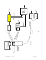
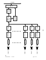
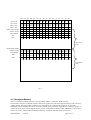
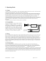
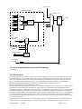
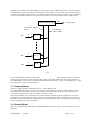
MuSTARD
1. Overview
MuSTARD (Multichannel Semiconductor Tracker ABC(D) Readout
Device) is designed to receive, store and decode the data from multiple Atlas SCT ABC(D)
modules in either the TSP (testbeam setup) or the System Test at CERN. It may also find use
in multiple-module production-test systems.
There are 12 input streams. Each stream is synchronised to the system clock and buffered in a
FIFO.
The readout control circuit event-builds the stream data and outputs complete events to the
host via a multipage dual-port memory. It also provides the capability of histogramming hit
channels on the fly without incurring a time penalty. MuSTARD is an electrical module, ie its
data inputs are electrical, differential LVDS. Fig 1 shows the role of MuSTARD in a readout
system and fig 2 shows the main features of MuSTARD.
1.1 Format
MuSTARD is a 6U single width VME module. It is an A32 module, but may be operated for
test purpose as an A24 module, this mode being selected by means of a jumper. All transfers
are D16, programmed. Block transfer is not supported. An address space of 1 Mbyte is
occupied, with a 12-bit base address selectable by 3 hex switches. (In the A24 test mode only
the least significant switch is functional) MuSTARD responds to AM codes 9,A,D and E in
A32 mode and 39,3A,3D and 3E in A24 mode. DTACK is asserted for any 16-bit transfer
within the 1 Mbyte address space. BERR is never asserted.
1.2 power requirements
MuSTARD requires +5V and -5.2V.
The -5.2V may be provided via the JAUX connector if used in a CERN standard crate or via
the J2 connector if used in a normal VME crate. In this case the user has to provide -5.2V and
0Vat the appropriate J2 pins. The pins used are compatible with the VXI standard and are the
same as on the SEQSI. However, because MuSTARD requires J2 to be present, the ground
and -5.2V connections to J2 are made via jumpers, allowing these pins to be isolated if
required.
1.3 Front Panel Connectors
A 26-pin header connects the 12 LVDS inputs. A 10-pin header connects clock and command
signals from the Clock/Trigger system and carries a BUSY signal from MuSTARD to the
Clock/Trigger system.
Test sockets are provided to allow the synchronised signals (multiplexed) to be scoped.
1.4
Front Panel LEDs
LEDs indicate some of the module states, eg Fifo Full.
MuSTARD.doc
17/09/98
page 1 of 15
MuSTARD.doc
17/09/98
page 2 of 15
Junction Cable
or "dog-leg"
pigtail
low-mass A
opto
board
M O D U LE
b
a fi
le)
fig 1
low-mass B
clo
1 p ck, co
er
m
mo man
dul d f
ibre
e
s
da t
r es
er
(2 p
du
mo
BILED
Host
conventional
clock, ctrl
Oxford
FOD
module
opto receiver
busy
high volts
low volts
?
?
Host
clock,
trigger
system
clock,ctrl
MuSTARD
Host
2.
MuSTARD.doc
17/09/98
page 3 of 15
stream 0
stream 1
stream 2
stream 11
+
_
_
+
+
_
+
_
prog delay
prog delay
prog delay
prog delay
control logic
control logic
control logic
control logic
fig 2
9
9
9
9
FIFO
FIFO
FIFO
FIFO
histogram
memory
stream
readout logic,
decoder
event
output
buffer
I/F
VME
VMEBUS
VME Functions and Address Map
Fig 3 shows the VME address map. There are 3 areas, the CSR registers, the Event Output Buffer and the
Histogram Memory. All addresses are relative to the base address.
2.1 CSR Registers
All transfers to these registers are 16-bit, aligned to even byte boundaries.
2.1.1 Register 0, Module Reset
Base Address. Write only.
Module Reset. The module is reset by writing 1 to d0, then writing 0 to d0 to release the reset.
d0
All other bits ignored.
2.1.2 Register 1, Readout Control
Base Address + 2. Read and write.
MRDOEN when 0, transfer from the fifos to either the output buffer or the histogram memory is
d0
inhibited and VME access to the histogram memory is enabled. When 1, transfer from the fifos is enabled, and
VME access to the histogram is prevented. VME access to an output buffer page is enabled, but only when an
event is available to be read.
MDAQEN When 0, writing to the fifos is inhibited.
d1
d2:15 are ignored when writing.
d2,3,5,6 and 7 are zero when read, d4 indicates the state of the I2C bus, see later.
d8:15 are undefined.
MDAQEN and MRDOEN are cleared when Module Reset is asserted.
2.1.3 Register 2, Readout Mode
Base Address + 4. Read and write.
Sample_All. If sample_all is true, then readout from the fifos takes place only if one of the 4 pages of the
d0
output buffer is available. If it is false then readout from the fifos takes place as fast as possible, with the hit
channels being histogrammed and events going to the output buffer as pages become available.
Raw_Mode. In this mode (d1 = 1) the data is written to the output buffer without being decoded. The data
d1
is written to the output buffer as 16-bit words with d(15:13) being zero, d(12:9) indicate the stream number, d(8) is
a marker bit indicating end of a stream event, and d(7:0) is the stream data.
In Decoded Mode (d0 = 0) the data is decoded acording to the ABC(D) protocol and then written to the output
buffer. The decoded data format is shown later, in the section on the output buffer.
d2:15 are ignored when writing.
d2,3,5,6 and 7 are zero when read, d4 indicates the state of the I2C bus, see later.
d8:15 are undefined.
2.1.4 Register 3, Clock Control
Base Address + 6. Read and Write
d 0 USEXCK Allows the internal 40 MHz oscillator to be used for test purposes.
d1:15 are ignored when writing.
D1:3,5:7 are zero when read, d4 indicates the state of the I2C bus, see later.
d8:15 are undefined.
2.1.5 Register 4, Test Mode
Base Address + 8. Read and Write
d(1:0) selects the test operating mode.
d2:15 are ignored when writing.
d2,3,5,6 and 7 are zero when read, d4 indicates the state of the I2C bus, see later.
d8:15 are undefined.
MuSTARD.doc
17/09/98
page 4 of 15
2.1.6 Register 5, Status Register
Base Address + A. Read only.
The significance of the bits will be explained in more detail later.
d 0:3
SADD 0:3
The stream address. Generated by the stream readout logic.
d4
MDAQEN
Enables data to be written to the fifos.
d5
MRDOEN
Enables data to be read from the fifos.
d6
RD_PAGE 0
The output buffer has 4 pages, RD_PAGE 0,1 select a page for reading.
d7
SSTAT
Indicates to the stream readout logic if the stream being addressed is enabled.
d8
SDAV
Indicates to the stream logic if the stream being addressed contains data.
d9
SREN
Stream Read Enable. The signal issued by the stream readout logic to read data from the
fifos.
d 10
TRH*
Trigger Hold. This signal is asserted (active low) when an enabled streams fifo almost
full,
or when an enabled stream’s trigger count exceeds the programmed limit.
d 11
BCO_OK
Indicates that there has been no interruption of the beam crossing clock detected since
the last
Module Reset
d 12
RD_PAGE 1
d 13,14 WRITE_PAGE 0,1 2-bit address of the next page of the output buffer available for writing.
d 15
Always 1.
2.1.7 Register 7, Test Fifo
Base Address + C. Write only.
d 13:0 sends data to the TEST FIFO. The test fifo allows programmed test data to be sent to the stream storage
fifos, thus permitting all the main MuSTARD functions to be tested.
d 14,15 ignored.
2.1.8 Register 8, Test Trigger
Base Address + 10. Write only
Data ignored, initiates the transfer of test data from the test fifo to the stream storage fifos.
MuSTARD.doc
17/09/98
page 5 of 15
control and status
0
control and status
8000
event output
buffer m em ory
0
2
4
6
8
A
E
10
10000
histogram m em ory
80
A6
m odule reset
readout control register
readout m ode register
clock control register
test m ode register
status register
test fifo
generate test trigger
delay chips
100
stream logic
'm us-bus'
1FFFF
17E
stream logic
delay chips
80
82
84
86
90
stream 0
stream 1
stream 2
stream 3
stream 4
stream 5
stream 6
stream 7
100
104
108
10C
110
stream 0 m ode register
stream 0 trig lim it
stream 0 PAF reg
stream 0 status reg
stream 1
120
stream 2
130
stream 3
s tre am s 4:9
A0
stream 8
stream 9
stream A
stream B
1A0
1B0
MuSTARD.doc
17/09/98
stream A
stream B
page 6 of 15
2.2 Delay Chips
There are 3 4-channel delay chips per MuSTARD. Each channel delays the input data by 0-24 nS, selectable in
steps of one nS ie 5 bits, d(4:0). These chips are written to by transfers to base_address + 80 + 0,2,4,6 for streams
0-3, base_address + 90 + 0,2,4,6 for streams 4-7 and base address + A + 0,2,4,6 for streams 8-11. These transfers
are normal VME writes.
Data is transferred automatically to the chips by the I2C serial protocol, and each transfer takes approximately 200
μS. This area (80- A7 inc) is write only, but reading any of registers 1,2 or 3 gives the status of the transfer, d4 =
1 means transfer is taking place. A new transfer should not be initiated until the previous one has concluded. Only
data in the range 0-24 inc. should be written to the delay chips.
2.3 Stream Logic
There are 2 registers associated with each stream and 2 registers associated with each group of 4 streams.
2.3.1 Stream Mode register
Base address + 100 + Stream Number * 10. Read and write. One register per stream.
When writing,
Stream Enable
d0
d 1:15 ignored.
When reading,
d0
Stream n Enabled
d1
Stream n + 1 Enabled
d2
Stream n + 2 Enabled
d3
Stream n + 3 Enabled
where n is 0 for stream numbers 0 to 3, 4 for stream numbers 4 to 7 and 8 for stream numbers 8 to 11.
d 4 is zero
d 5:15 undefined.
2.3.2 Stream Status Register
Base address + 10C + Stream Number * 10. Read only. One register per stream.
d 0 Fifo Empty Flag. When d0 is 1 then the fifo contains no data.
d 1 Almost Full flag. When d1 is 1 then the fifo is Almost Full.
d 2 Trigger Overflow. When d2 is 1 it indicates that the stream’s trigger counter - which counts up for received
L1
triggers and counts down for events received from detector data streams - contains a number greater
than the programmed limit for that stream.
d 3 Fifo Full Error Flag , when d4 is 1 it indicates that the FULL FLAG of the fifo has been asserted at least once
since MDAQEN was last asserted. When a fifo’s FULL FLAG is asserted it is likely that data will have been lost.
All Fifo Full Flag Error Flags are cleared when MDAQEN is deasserted.
d 4 Trigger Count Error Flag. This signal is set when the Trigger counter indicates that the number of L1
triggers
received exceeds the number of events received by more than 30, or that the number of events received
exceeds the number of L1 triggers received. All Trigger Count Error Flags are cleared when MDAQEN is
deasserted or when a RESET COMMAND is detected.
d 5:15 are undefined
2.3.3 Trigger Limit Register
Base address + 104 + Stream Number * 10. Read and write. One register per 4 streams. One register corresponds
with streams 0-3, the second register corresponds with streams 4-7, the 3rd register corresponds with streams 8-11.
d 0,1 TLR 0,1. These 2 bits determine the value of trigger count at which Trigger Overflow is set.
When TLR 1:0 = 0, trigger overflow occurs when the trigger count is greater than 3
When TLR 1:0 = 1, trigger overflow occurs when the trigger count is greater than 7
When TLR 1:0 = 2, trigger overflow occurs when the trigger count is greater than 15
When TLR 1:0 = 3, trigger overflow does not occur.
d 15:2 are ignored when writing.
When reading,
MuSTARD.doc
17/09/98
page 7 of 15
d 2:4 are zero, d 3:15 are undefined.
2.3.4 PAF Register
Base address + 108 + Stream Number * 10. Read and write. One register per 4 streams. One register corresponds
with streams 0-3, the second register corresponds with streams 4-7, the 3rd register corresponds with streams 8-11.
Each fifo has a Programmable Almost Full flag. Writing to the PAF register causes the register value to be
written to the fifos as an offset from full at which the PAF will be asserted.
d 0,1 PF0,1. The offset from full is the value of PF 1:0 * 2K + 2K.
2.4 Output Buffer
The output buffer is a 4-page dual-port ram, each page being 16K*16, with the pages being controlled by a fifolike circuit. MuSTARD writes one complete event to one page. The buffer is full when it contains 4 unread events.
To the host, the memory looks like a single 16Kword page, starting at Base Address + 8000. Only complete events
are made available. The host must determine the availability of an event by reading the first word of the memory.
A negative value (ie bit 15 set) indicates that there is no data available. In fact when the first memory location is
read and no event is available it is the data from Status Register which is actually read.
The availability of an event is signalled by the value of the first word being positive, ie with bit 15 = 0. The number
of words in the event are indicated in bits 13:0. If bit 14 is set it indicates that an error (either an error code from
the front-end chips or a protocol violation) was detected at some point in the event. Error detection and counting
only occurs when running with Decoded Mode. When the host has finished with an event it must signal this to
MuSTARD by writing to the first memory word (data ignored).
When running in DECODED Mode (RAW_MODE = 0) the data format is as shown in fig 4.
When running in RAW Mode the data is transferred directly from the stream fifos with no alteration. In this case
the format is: d8:0 is raw fifo data, with d8 indicating the end of a stream’s event. d 12:9 indicate the stream
number.
MuSTARD.doc
17/09/98
page 8 of 15
d15 d14 d13 d12 d11 d10 d9
word count
error count
E
d8
d7
d6
d5
d4
d3
d2
d1
d0
w13 w12 w11 w10 w9
w8
w7
w6
w5
w4
w3
w2
w1
w0
er15 er14 er13 er12 er11 er10 er9
er8
er7
er6
er5
er4
er3
er2
er1
er0
event count
ec15 ec14 ec13 ec12 ec11 ec10 ec9 ec8 ec7 ec6 ec5 ec4 ec3 ec2 ec1 ec0
event count
ec31 ec30 ec29 ec28 ec27 ec26 ec25 ec24 ec23 ec22 ec21 ec20 ec19 ec18 ec17 ec16
stream event header
1
0
0
stream number
0
0
strip address
t3
t2
t1
t0
b7
b6
b5
b4
b3
b2
b1
b0
s3
s2
s1
s0
0
1
0
0
a2
a1
a0
data
0
0
1
d2
d1
d0
data
0
0
1
d2
d1
d0
c3
c2
c1
c0
a6
a5
a4
a3
1st stream
event
stream event header
stream number
strip address
1
b2
b1
b0
s2
s1
s0
a3
a2
a1
a0
1
d2
d1
d0
1
d2
d1
d0
0
0
0
0
0
1
0
0
0
0
0
data
data
b3
s3
0
t3
t2
c3
t1
c2
t0
c1
b7
c0
b6
a6
b5
a5
b4
a4
next stream
event
fig 4
2.5 Histogram Memory
This is a 32 Kword (64 Kbyte) memory, starting at Base Address + 0x10000 Read and write.
Each stream is assigned a 2 Kword segment. Within the segment, hit strips are mapped according to the 7 bit strip
number and the 4 bit chip number. Normally only 768 locations of a 2 K segment will be active, but if the
redundancy scheme whereby the data of 2 sides of a module can be routed to a single fibre is used then 2 groups of
768 words will be active. The histogram memory can be accessed from VME only when MRDOEN is not asserted.
There is no “clear” command for the histogram memory, it must be cleared by writing zeroes to it.
MuSTARD.doc
17/09/98
page 9 of 15
14
13
S3 S2
12
11
S1
S0 C3
S tre a m N u m be r
MuSTARD.doc
17/09/98
10
9
8
7
6
C 2 C1 C 0 a6
C h ip N um b er
5
4
3
2
1
0
a5
a4
a3
a2
a1
a0
S tr ip N um ber
page 10 of 15
3. Operating Guide
3.1 Clock
A “Beam Crossing” clock (40 MHz) is input to MuSTARD at differential ECL levels on pins 7 and 8 of the frontpanel mounted 10-pin IDC plug. This clock is used as the system clock.
A 40 MHz crystal oscillator is used as the frequency reference for the delay chips, and may also be used for test
purposes to replace the BC clock for all functions. This is implemented by writing to the Clock Control Register.
The VME Interface circuit itself requires a clock. This is normally the BC clock. However to avoid the VME
Interface hanging up if the BC clock (an external signal) was lost MuSTARD includes a circuit which
continuously compares the frequency of the BC clock to that of the internal 40 MHz crystal clock and if they are
not approximately the same the VME interface is switched to the crystal clock until the BC clock is restored. This
feature only allows the VME Interface to continue functioning but most of the other circuits will be nonfunctioning.
A jumper (pl )allows the frequency checking feature to be disabled.
3.2 Control Data
This is the signal used to send L1 triggers and other
commands to detector modules. It is input to
MuSTARD as differential ECL on pins 9 and 10 of
the 10-pin plug. As a Data Receiver MuSTARD does
not make direct use of this signal in its data
acquisition, but it can be used to keep track of the
number of unread events in the front-end buffers.
The data is decoded to extract the L1 triggers and
the Soft Reset. All other commands are ignored.
Control Data
9
10
+
_
Trig
Control Data Decoder
reset
470 0hm
front panel
lemo skts
470 0hm
3.3 Busy
Busy is a differential ECL signal which is output by MuSTARD as differential ECL on pins 1 and 2 of the 10-pin
plug. It is asserted if any enabled stream’s fifo has sufficient data that its Almost Full Flag is asserted, or if any
enabled stream’s “trigger count” exceeds the programmed limit. The trigger count is a counter, one for each
stream, which is incremented when an L1 trigger is detected on the Control Data input and decremented when a
trailer (ie end of event) is detected on a stream. The busy signal may be used to inhibit further triggers until it is
de-asserted. The contribution of the trigger counters to Busy can be turned off ( by writing 3 to the Trigger Limit
Registers associated with enabled channels) but the contribution by the Almost Full Flags can not, other than by
disabling a stream.
3.4 Stream Inputs
There are 12 input streams at LVDS levels on pins 1 to 24 of the 26 pin front panel mounted IDC plug.
Pins 25 and 26 of this plug may be connected to ground by means of a jumper, PL3, or they may be left open.
The inputs are latched by the BC clock. Since the inputs have arbitrary phase relative to this clock they are first
delayed. This is done using 4 channel delay chips produced by ..........A.Marchioro and T.Toifl…….
The outputs of the delay chips are latched. Delayed signals are multiplexed in 3 groups of 4 to 3 Lemo front panel
sockets. The latch clock is also output to a Lemo socket so that the delayed signals can be observed relative to the
clock. The multiplexing of the 3 groups of 4 delayed signals is controlled by a 2-bit counter which is incremented
by pressing the front-panel push-button switch. The state of this counter and hence which of the 4 streams can be
monitored is indicated by 2 LEDs.
MuSTARD.doc
17/09/98
page 11 of 15
from test fifo
3 identical circuits
12-bit 2-1 mux
+
12
_
12
+
_
4 channel
delay chip
+
12-bit
latch
to fifo logic
4
4
_
4
+
_
front panel
lemo skt
470 0hm
4-1
MUX
front panel
LEDs
front panel switch
front panel
lemo skt
2 bit
c oun ter
470 0hm
Clock
3.5 Serial to Parallel Conversion and Fifo Writing
To be added.
3.6 Fifo Readout
Fig 7 indicates the way the fifos are readout. Note that for simplicity a fifo and the considerable amount of logic
associated with it are represented by a single box and that in the description which follows reference is made to
“fifo” even though the actual signal source or destination may be the associated logic rather than the actual fifo
chip. A more precise and complete description of the MuSTARD circuits will be found in the MuSTARD
TECHNICAL REFERENCE MANUAL written by NN which will be available early in YY.
Readout of the Fifos begins when MRDOEN is asserted.
The Stream Readout logic generates a 4 bit address. Each Fifo is addressed in turn. If the stream is enabled, this is
indicated by the fifo asserting the signal SSTAT. If this signal is not asserted then the Stream Readout logic
increments the address to interrogate the next fifo. When an enabled fifo is found it may or may not have any data.
The Stream Readout logic requests a data word and if one is available the fifo presents the word on the data bus
and asserts the signal SDAV. The Stream Readout logic continues to request data until it receives a word with bit 8
set, which indicates the end of a stream’s event. When it receives this end of event signal the Stream Readout
logic increments the address and interrogates the next fifo. This process continues until all enabled fifos have had
an event read from them.
2 points need to be noted. The first is that MuSTARD is basically a dumb circuit and once an enabled stream is
found it will continue to request data from it until the end of event is indicated. If, for any reason, no data is
MuSTARD.doc
17/09/98
page 12 of 15
available on an enabled stream MuSTARD will sit waiting for it until it (MuSTARD) is reset. The host computer
should implement a time-out system to avoid hang-ups. The second point to note is that the event building process
is based on the assumption that the first event in each (enabled) fifo is derived from a common trigger, and that if
events are assembled by reading just one event from each fifo in turn then all streams remain in step and each
Stream Readout Logic
4-bit Stream Address,
SADD
data
to output buffer
9-bit data bus +
SSTAT, SDAV
9
data
fifo 11
9
data
fifo 1
9
data
fifo 0
fig 7
event read from MuSTARD will represent data from a single trigger. If a trigger should be missed in a stream, or
should a stream end-of-event not be recognised then stream event synchronism will be lost and will remain lost
until MuSTARD is reset. The host computer should therefore check the data - at least on a sampling basis - so that
out-of-step stream events will be recognised.
3.7 Sampling Modes
There are 2 sampling modes, SAMPLE ALL and ….NOT SAMPLE ALL.
The output Buffer can hold up to 4 events, after which it has no more space available. When SAMPLE ALL is
selected, then when the buffer is full the stream readout is halted and resumes only when space for at least one
event becomes available. All events are therefore accessible to VME.
When NOT SAMPLE ALL is selected then the stream readout proceeds at the fastest possible rate. An event is
transferred to the output buffer only if there is space for it at the beginning of the event readout. The purpose of
this mode is to allow accumulation of histogram data at the fastest possible rate while allowing the host to sample
events so that data quality can be monitored.
3.8 Readout Modes
There are 2 readout modes, RAW mode and DECODED mode, selected by writing 1 or 0 to Raw_Mode, bit 1 of
Register 2.
MuSTARD.doc
17/09/98
page 13 of 15
In Raw mode the 9-bit data words from the fifo are written to the output buffer without any change other than the
addition of the 4-bit Stream Address in bits 12:9.
15 14 13 12 11 10
0
0
0
9
8
7
6
5
4
3
2
1
0
s3 s2 s 1 s 0 eos d7 d6 d5 d4 d3 d2 d1 d0
Bit 8, eos, indicates the end of a stream’s data. When a detector module outputs an isolated event then when eos is
set bits 7:0 will be zero, but if events are output with less than 8? clock periods between the end of a trailer and the
beginning of the next event then these bits may have part of the header bits of the next event. These bits should be
ignored other than for diagnostic purposes. The next event, as do all events, will begin left justified to bit 7.
In Decoded mode the data from the fifo is decoded according to the ABC protocol, and written to the output buffer
with the format shown in fig n. Note that only “real” data is decoded correctly, configuration data is not and in fact
if configuration data is received it will be tagged as an error. If it is required to read configuration data then RAW
mode must be selected. The data output of a master set to clock_through mode will result in errors.`
Note that there is no point running in NOT SAMPLE ALL mode if RAW mode is selected, as histogram data can
only be accumulated in DECODED mode.
In DECODED mode the data is decoded and output with the form as shown in fig 4.
In both RAW and DECODE modes the 4 word header is output, but in Raw mode the error count and error bit
have no significance. In both modes bits 13:0 indicate the number of words in the event including the header
words. In decoded mode the error count indicates the number of events in which errors have been detected since
the MuSTARD module was last reset. The 32 bit event count gives the number of events read from the fifos since
the last reset. Note that in NOT SAMPLE ALL mode this number is the number of events read from the fifos, not
the number read via the output buffer.
3.9 The Output Buffer
The output buffer is a Bank Switched Dual Port Memory (IDT 707288S)
This is a 64K*16 bit memory, divided into 4 16K*16 banks or pages. Each of these pages can be assigned (that is
have read and write access) to either the left or right ports. The Left Port is written to by MuSTARD, the Right
Port is the only port accessible to VME. The scheme implemented in MuSTARD is that all pages are assigned to
MuSTARD initially. Then when an event is written to a page it is assigned to the right port ie for VME access.
Only one page at a time is assigned to VME access, the one containing the oldest data. The assignment of a page to
the Right or VME port is done only when a complete event has been written. If an attempt is made to read from the
buffer when a page is not assigned for read then the results will be undefined. Although an assigned page can be
read and written, it should not be written to other than as part of (expert?) fault diagnosis.
4. Initialisation
It is important to note that MuSTARD is a dumb data receiver and therefore when initialising it the Host must
control the trigger system so that data can be prevented from being received by MuSTARD before it has been
correctly initialised.
4.1 Module Reset
When asserted, Module reset clears MDAQEN and MRDOEN.
The fifos are reset, ie they are emptied of data and the almost_full pointer is set to the default value.
The trigger counters are cleared.
The output buffer pointers are cleared, and all 4 pages are assigned to the left port, ie they are cleared and the
VME has no access, since there is no event available to be read.
Note that the histogram memory is not cleared, but the VME now has access and may clear it by writing zeroes to
all locations.
MuSTARD.doc
17/09/98
page 14 of 15
4.2 Registers to be loaded
4.2.1 Stream Enable
Each fifo has associated with it a mode register. Only bit 0 is significant. This bit, when set, enables data to be
written to the corresponding fifo when MDAQEN is asserted. This register is addressed at base-address + Streamnumber * 10.
4.2.2 Trigger Limit
Associated with each input stream is a counter which, when the stream is enabled counts up when an L1 trigger is
received and counts down when the end of an event is detected. The value of the counter is compared with a value
in a trigger limit register. There are 3 registers, one associated with fifos 0:3, one with 4:7 and one with 8:11.
These registers may be addressed respectively at base-address + 104, ba + 144 and ba + 184.
Only bits 0,1 are significant. When these bits are set to 0 the trigger limit is 4, when 1 the limit is 8, when 2 the
limit is 16 and when set to 3 there is no limit.
4.2.3 PAF – Programmable Almost full
Each fifo has a flag which is set when the fifo contains 128K – N bytes (or more) of data.
N can be selected by writing to the PAF register. There are 3 registers, one associated with fifos 0:3, one with 4:7
and one with 8:11. These registers may be addressed respectively at base-address + 108, ba + 148 and ba + 188.
Only bits 0,1 are significant. When set to 0 N is zero, when set to 1 N is 2K, 2N is 4K and when these bits are set
to 3 then N is 6K.
4.3 Diagnostic information
to be added
Maurice Goodrick
Martin Morrissey
MuSTARD.doc
[email protected]
[email protected]
17/09/98
page 15 of 15