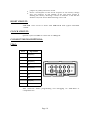
1
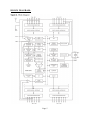
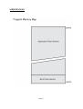
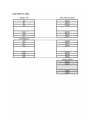
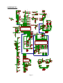
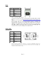
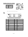
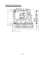
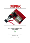
AVR-GSM development board
Users Manual
All boards produced by Olimex are ROHS compliant
Rev. C, October 2011
Copyright(c) 2011, OLIMEX Ltd, All rights reserved
Page 1
INTRODUCTION:
AVR-GSM is excellent board for adding remote monitoring and control in
remote places by GSM cellular network. Do you want to switch on/off
your local heating in your mountain house? To monitor the temperature at
up to 8 remote points up to 30 meters away from the module? To listen
what happens in your house with silent call after you get message for
alarm status? Then AVR-GSM is the board for you! It contains ATmega32
microcontroller and 3-band GSM GPRS module 900/1800/1900Mhz inside
which covers most used GSM networks around the world. The GSM
antenna is build in the board so no need for external expensive GSM
antennas. AVR-GSM have two relays 240VAC/10A, two opto-isolated
inputs which could be connected to alarm sensors or just buttons for user
actions (like call pre-loaded phone numbers), on-board temperature sensor
and connector for additional up to 8 addressable remote temperature
sensors at up to 30 meter distance from the module. Normal phone hook
can be connected to this board and to allow user to speak, listen, taking
and placing phone calls as normal stand alone cellular phone. AVR-GSM
can be connected to PC with the USB connector it have and it is recognized
as modem which could be used to add internet via GPRS to your computer
(imagine how useful is this for your mountain house if there is no internet
but only cellular network!).
BOARD FEATURES:
•
•
•
•
•
•
•
•
•
•
•
•
•
•
•
•
•
MCU: ATMega32 32KB Flash memory, 2KB RAM, 1KB EEPROM
JTAG connector for programming and debugging with AVR-JTAG-L
or AVR-JTAG-USB
GSM GPRS 3-BAND MODULE 900/1800/1900Mhz with build onboard GSM cellular antenna
Li-ion backup battery for up to 200 hours of GSM module stand-by
(no relays etc - peripherals active)
SIM-card holder
Two RELAYS 240VAC/10A
Two opt isolated inputs
USB interface
2.5mm Hands-free connector;
Buzzer (ringer)
Status LED
On-board temperature digital sensor
Connector for remote temperature sensors up to 30meters far away
from AVR-GSM
Plastic housing (optional)
Extension 26 pin connector for all unused ATMega32 ports
PCB: FR-4, 1.5 mm (0,062"), solder mask, silkscreen component
print
Dimensions: 130x82x34 mm (5.1x3.2x1.3")
ELECTROSTATIC WARNING:
The AVR-GSM board is shipped in protective anti-static packaging. The
board must not be subject to high electrostatic potentials. General practice
for working with static sensitive devices should be applied when working
with this board.
Page 2
BOARD USE REQUIREMENTS:
Cables:
1.8 meter USB A-B cable to connect to USB host on PC.
Hardware:
AVR-JTAG, AVR-USB-JTAG
Or any compatible tool for programming and/or debugging
Software:
AVRStudio + WinAVR for developing your own applications
The demo software show basic functionality and how to place /
take phone calls (C source and HEX) or how to remote control
via SMS (C source and HEX)
The sources are compiled with WinAVR free C compiler.
Important: If your board does not work, first try to charge the battery as
you power supply the board for few hours.
PROCESSOR FEATURES:
•
•
•
•
•
High-performance, Low-power AVR® 8-bit Microcontroller
Advanced RISC Architecture
– 131 Powerful Instructions – Most Single-clock Cycle Execution
– 32 x 8 General Purpose Working Registers
– Fully Static Operation
– Up to 16 MIPS Throughput at 16 MHz
– On-chip 2-cycle Multiplier
Nonvolatile Program and Data Memories
– 32K Bytes of In-System Self-Programmable Flash Endurance:
10,000 Write/Erase Cycles
– 1024 Bytes EEPROM Endurance: 100,000 Write/Erase Cycles
– 2K Byte Internal SRAM
– Programming Lock for Software Security
JTAG (IEEE std. 1149.1 Compliant) Interface
Peripheral Features
– Two 8-bit Timer/Counters with Separate Prescalers and
Compare Modes
– One 16-bit Timer/Counter with Separate Prescaler, Compare
Mode, and Capture Mode
– Real Time Counter with Separate Oscillator
– Four PWM Channels
– 8-channel, 10-bit ADC with Programmable Gain at 1x, 10x, or
200x
– Byte-oriented Two-wire Serial Interface
– Programmable Serial USART
– Master/Slave SPI Serial Interface
– Programmable Watchdog Timer with Separate On-chip Oscillator
– Power-on Reset and Programmable Brown-out Detection
Page 3
Page 4
BLOCK DIAGRAM:
Page 5
MEMORY MAP:
Page 6
Page 7
USB
R35
R36
C7
10n
GND
+
Page 8
R18
22K
1K
RELAY2
39
ATMEGA32_4 4TQFP
GND2
GND1
GND
USB_PRESENT
BUZ
B1
IN2
LED
SCL
RELAY1
RELAY2
PC5
PC4
PC3
PC2
SDA
PC5
PC2
PC4
PC3
EXT-24 3 V
EXT-1 6
EXT-1 8
EXT-2 0
EXT-2 2
JTAG
RXD
TXD
RI
1
3
5
7
9
2
4
6
8
10
RST
3V
R45
2K/1%
R44
20K/1 %
CON8PH
8
7
6
5
4
3
2
1
O PT_ TEMP
EXT-8
2K
R7 9
Z2
R75
33K
3 30
330
D2
1N4148
R24
D6
1 N4148
R25
BZV55C5V1(mini-melf)
R4 1
10
3V
SCL,SDA
NETLIGHT
2
LED2
red 1
2
3
4
3
4
IN1
H11A817 SMD
OPT1
4V
NA
R8 2
4.7 K
R32
4 .7K
R26
3V
2
3V
3V
R12
2K
R81
33K
D4
1 N4148
1N414 8 2K
D5
IN2
SDA
SCL
H11A817SMD
LED3 OPT2
red 1
SDA
SCL
C27
1
1000u F/6 .3V/8x12/low_ESR
BUZ
Q4
BC817
STAT
red
VBAT
2
47u F/6 .3V
C5
0
+5V
C62
R8
1K
R7
1K
U2
SDA VDD
SCL
ALERT A0
A1
GND A2
TCN75A(NA)
4
1
2
3
Q5
BC817
BUZ
PB1221
R40
1K
0
R2
22K
B1
7
6
5
8
3V
http ://www.olimex.co m/dev
+5V
3V
3V
3V
VBAT
1 00n
C4
3V
100 n
C22
COPYRIG HT(C) 2 009, O LIMEX Ltd
Rev. B
GND
C60
EXT-11
1n(NA)
LED
LED
EXT-3
EXT-5
EXT-7
EXT-9
PWRKEY
6x3.8x2.5/SMD
4
5
6
R33
330
SIM
SIM-HO LDER
VCC
SIMRST SIMNC
EXT-13 R38
NA
PWRKEY
AVR-GSM
3V
C8
10 0n
R39
C63
220n (N A)
C61
2.2 uF(NA)
VBAT
VBAT
330p (N A)
1
1 0K
SIMCLK SIMIO
R2 3
2
3
2
R 17
1
TXD,RXD,R TS,CTS,DTR,DCD,RI,DBG_TX,DBG _RX,MAIN_RX,MAIN_TX
+
T4
BC817
3
MAIN_RX
MTX/DTX
18
6
16
15
14
13
12
11
10
9
26
25
24
23
22
21
20
19
IN1
STATUS
USB_RST
EXT-1 0
EXT-1 2
EXT-1 4
PC[0..7]
100 n
C13
(OC2)PD7
(ICP)PD6
(OC1A)PD5
(OC1B)PD4
(INT1)PD3
(INT0)PD2
(TXD)PD1
(RXD)PD0
(TOSC2)PC7
(TOSC1)PC6
PC5(TDI)
PC4(TDO)
PC3(TMS)
PC2(TCK)
PC1(SDA)
PC0(SCL)
(SCK)PB7
(MISO)PB6
(MOSI)PB5
(SS)PB4
(AIN1)PB3
(AIN0)PB2
(T1)PB1
(T0)PB0
PWRKEY
RTS
CTS
DTR
DCD
D10
100 n
C14
VCC2
VCC1
VCC
AGND
AVCC
AREF
3
2
1
44
43
42
41
40
30
31
32
33
34
35
36
37
1N4148
D9
100 n
C12
38
17
5
28
27
AREF 29
1 0uF/6.3V
C2 1
XTAL1
(ADC7)PA7
(ADC6)PA6
(ADC5)PA5
(ADC4)PA4
(ADC3)PA3
(ADC2)PA2
(ADC1)PA1
(ADC0)PA0
1N4148
1 N4148
D1
2
3V
330
1 0uF/6.3V
C3 4
R3 4
8
XTAL2
RESET
R74
560
D8
1N4148
RXD
DBG_R X
2
1
MAIN_TX
TXD
DBG_TX
L2
FB(080 5)
7
4
Q3
7.3 7MHz
RST
22
D7
RAS1 215
REL2
RELAY1
3V
C11
22pF
C3
22p F
+1 2V
AGND
SIM300D_HD_V2
17
30
31
32
34
35
36
37
48
1N4148
LED_ R2
R 19
22K
1K
R11
1N4 148
EXT-2
EXT-4
EXT-6
NA
C 19
U6
C10
100 n 10p
C16
close to module
10p
C18
EAR+
RERAUDIOOUT+
AUDIOOUT-
GND1
GND2
GND3
GND4
GND5
GND6
GND7
GND8
GND9
1
5V_CHG_E
22
22
22
B1
+12V
T3
BC81 7
18
REL2
7
25
+
RAS12 15
26
21
D12
3VA
RESET 1
P-
EXT-2 6
33p
33p
close to connecor
C78
C74
23
24
26
25
MIC2P
MIC2N
MIC1N
MIC1P
ANTENNA
NA
NA
+
GND
+
TXD,RXD,RTS,CTS,DTR,DCD,RI,DBG_ TX,DBG_RX,MAIN_RX,MAIN_TX
2
1
18
19
20
21
33
NETL IG HT
R48
R47
R2 2
SIMRST
EXT-1
R 21
SIMCLK
VSIM
R2 0
SIMDATA
10uF/10V/1206
33p
SPEAKER
H EAD2
10uF/12 06
A1
GSM_ PCB_ANT
38
39
41
12
27
29
15
28
9 VSIM
6 SIMDATA
7 SIMCLK
8 SIMRST
47
0
R1
C58
2 VCC
10K
R14
U1
STM10 01R
C71
C6
33p
C23
BACKUP
VCHG
RXD
TXD
TEMP_BAT
DTR
AUXADC
RTS
CTS
NETLIGHT
RI
POWERKEY
DCD
DEBUG_TX
VBAT1
DEBUG_RX
VBAT2
SPI_D/C
KBROW0
U3
C2
10uF/6.3V
STATUS
VSIM
GPO1
SIMDATA
SPI_DATA
SIMCLK
SPI_CLK
SIMRESET
SPI_CS SIM_PRESENCE
R9
(NA)
R31
(NA)
220uF/10V/tant
C57
R16
2K
R1 0
2K
GND1
AGND
10
R43
33p
33p
close to microphone
C9
C20
33p
C77
3
4
43
44
45
11
42
2
1
5
40
14
13
46
16
10
NC/FB
/EN
+
33p
C73
MIC
MIC
68
4
3
+
1
red
LED_R1 REL1
GND2
REL1
C25
3V
JACK-3PIN PHON E_JACK_ UNI
3
2
1
HANDSFREE
33p
C76
EXT-1 5
EXT-17
EXT-19
EXT-21
EXT-23
EXT-25
MAIN_RX
MAIN_TX
DTR
R TS
CTS
RI
D CD
DBG _TX
D BG _RX
STATUS
C17
2.2uF
1N5819 S
1000u F/6 .3V/8x12/low_ESR
C 28
1N5819 S(NA)
1
100n
CBUS0
CBUS1
CBUS2
CBUS3
CBUS4
TEST
GND3
+12V
10 0n
C38
3V3OUT
FT232RL
17
23
22
13
14
12
DCD
RI
560
56 0
R30
R15
R42
-
R6
3 3K
R37
NA
24
27
28
NC1
#RESET
NC2
OSCI
OSCO
USBDM
USBDP
1000u F/6 .3V/8x12/low_ESR
C 46
+
1
2
3
4
5
6
10 0n
16
15
R4
4.7K
8
USB_RST 19
P+
R46
22K
USB_PRESENT
NA
NA
C36
RXD
TXD
RTS
CTS
D TR
560
560
560
560
560
R5
R13
R27
R28
R29
220uF/10 V/ta nt
C 47
TXD,RXD,RTS,CTS,DTR ,DCD,RI,DBG_TX,DBG _RX,MAIN_RX,MAIN_TX
10uF/10 V/120 6
C53
2
DOWNLOAD
REL
USBDM
USBDP
C26
10uF/6.3V
C37
C15
1
5
3
11
2
9
10
6
D3
1N582 2(SMC)
15uH/DBS135
0
3V_E
0
VBAT
2
CON6PH
0
0
2.2uF/0805
S H IE LD
TXD
RXD
RTS#
CTS#
DTR#
DSR#
DCD#
RI#
150 K
R71
+
VCCIO
VCC
C5 0
4 .7n
+
4
20
3
1
2
USB_PW R
EN/SYNC
GND FB
BD97 78HFP
7
4
4.99K/1 %
15K/1%
C24
1 0n
5
VSIM,SIMDATA,SIMCLK,SIMRST
FB1
R73
R72 4.7 K
68 K
R70
4.99K/1 %
OUT
+
U5
FT23 2RLSSO P2 8
1 00n
C52
L1
IN
VR(3V)
TPS770 30
1
LI_BAT
1
2
3
4
3V
C51
5
2
D1 1
P-
USB
USB_SHIELD
+
C1
1000 uF/16VDC
+
C29
1000 uF/16VDC
INV
SW
+5V
D14
+
12 V
VIN
RT
VR
1
6
USB_PWR
GND
1N40 04(SMD)
D15
+5V
D CD C_ E
1
1
2
C ON2PH
R3
NA
2
4 V_E
1
R69
3V
2
+12V
D13
1 N5819S
2
1
VBAT
BAT_ E
9 0-DEG REE
SCHEMATIC:
3
MRX/DRX
3
BOARD LAYOUT:
POWER SUPPLY CIRCUIT:
The power supply of AVR-GSM could be done in two different ways:
1. Power from +12VDC without using the internal backup battery.
The module is powered only from external 12V and the battery is not
connected. In this case:
− jumper BAT_E must be open
− jumper 4V_E must be closed
− jumper 4V must be closed
− jumper 5V_CHG_E must be open.
Power consumption in this mode is:
− about 60mA when have a conversation.
− About 25mA in normal mode (without conversation) + 60mA if
relays are turned on.
Important: 4V_E, 4V and 5V_CHG_E jumpers have to be
together.
moved
2. Power from +12VDC with backup battery.
The module is powered with battery and allows battery charging. In
this case:
− jumper BAT_E must be closed
− jumper 4V_E must be open
− jumper 4V must be open
Page 9
−
jumper 5V_CHG_E must be closed
− Power consumption in this mode: depend on the battery charge
may vary between 10 and 300mA. If the 12V power supply is
missing the battery discharge current is between 5 and 25 mA
without call, and about 200mA during active call.
RESET CIRCUIT:
AVR-GSM reset circuit is made with STM1001R with typical threshold
+2.63V.
CLOCK CIRCUIT:
Quartz crystal 7.37MHz is connected to ATMega32.
CONNECTOR DESCRIPTIONS:
JTAG:
Pin #
Signal Name
1
PC2(TCK)
2
GND
3
PC4(TDO)
4
3V
5
PC3(TMS)
6
RST
7
3V
8
NC
9
PC5(TDI)
10
GND
This connector allows programming and debugging via AVR-JTAG or
compatible tool.
Page 10
USB:
Pin #
Signal Name
1
VCC
2
USBDM
3
USBDP
4
GND
This is standard USB Type B
connector for connection to PC. On board there is FT232RL USB to UART
converter. To use it you should download and install the drivers for your OS
from
http://www.ftdichip.com/Drivers/CDM/CDM20602.zip.
ATMega32 can control FTDI chip as detect USB present and can toggle RST
line of FTDI chip, i.e. the microcontroller decides
whether the
communication is between PC terminal and GSM module or between
ATMega32 and GSM module. When USB cable from PC is connected to
AVR-GSM – ATMega32 allows communication between USB (PC terminal)
and GSM module, when USB cable is removed from AVR-GSM, the
communication is between ATMega32 and GSM module.
SIM-CARD:
Pin #
Signal Name
1
VSIM
2
SIMRST
3
SIMCLK
4
GND
5
NC
6
SIMDATA
This is standard SIM card connector, to operate AVR-GSM should have
inserted valid SIM card for your operator network. Note that the SIM card
should be without PIN security.
Page 11
PWR-CON :
Pin #
Signal Name
1
+12V
2
GND
This connector is used to power the AVR-GSM. External (12VDC) power
source have to be applied to this pins.
OUTPUT RELAYS CONNECTOR:
Pin #
Signal Name
1
NO-REL1
2
COMMON-REL1
3
NC-REL1
4
NO-REL2
5
COMMON-REL2
6
NC-REL2
NO – relay normally opened contact, NC – relay normally closed contact
COMMON – relay common contact
By this connector the user can switch on/off load witch not exceed next
maximal admissible ranges:
- 15A/125VAC
- 10A/250VAC
- 15A/24VDC
Page 12
INPUT OPTOCOUPLER & TEMP CONNECTOR:
Pin #
Signal Name
1
DIGITAL IN1 +
2
DIGITAL IN1 -
3
DIGITAL IN2 +
4
DIGITAL IN2 -
5
GND
6
SCL
7
SDA
8
3V
Two digital optoisolated inputs are available for user code. The input level
are between 5 and 12V DC.
I2C signals (SCL, SDA) are used for external temperature sensor connection
or other suitable I2C device interfacing.
There is possibility up to 8 external temperature sensors on this bus.
Olimex sell these modules separately under the order code MOD-TMP and
communication with up to 30 meters between the AVR-GSM and MOD-TEM
is possible error free.
HANDSFREE:
Pin #
Signal Name
GND
GND
AU+
AU+ audio out
MIC
MIC2P audio in
This
is
Audio
2.5
mm
connector.
Standard
headphone/microphone combined cable can be used
Page 13
hands-free
SPEAKER CONNECTOR - SPEAKER:
Pin #
Signal Name
1
EAR–
2
EAR+
This is connector for external 32 ohm speaker
EXT:
Pin #
Signal Name
Pin #
Signal Name
1
BACKUP
2
AREF
3
GND
4
3VA
5
3V
6
AGND
7
VBAT
8
(ADC3)/PA3
9
+5V
10
PWRKEY - (ADC2)/PA2
11
POWERKEY-pin12 of GSM
module
12
(ADC1)/PA1
13
AUXADC
14
(ADC0)/PA0
15
GPO1
16
(SCK)PB7
17
SPI_DATA
18
(MISO)PB6
19
SPI_CLK
20
(MOSI)PB5
21
SPI_CS
22
(SS)PB4
23
SPI_D/C
24
(T1)PB1
25
KBROW0
26
RST
Page 14
EXT is connector for external plug-in modules. It's standard 26 pin ribbon cable IDC keyed
connector.
Backup: RTC backup power supply for the GSM module real time clock and RAM, when the
battery is discharged. If the battery attached to this signal is chargeable and the voltage
level is low the module will charge the battery. Vnom = 1.8V, Inom= 20uA
AREF: Analog reference input of ATMega32 microcontroller. Can be used for external
analogue circuits.
GND: Digital ground.
3VA: Analog power supply of ATMega32 microcontroller. This is 3VDC output which can be
used for external analog modules.
3V: Digital power of ATMega32. This is 3VDC output for external digital modules.
AGND: Analog ground of ATMega32 microcontroller. Can be used for external analog
circuits.
VBAT: Dedicated to connect main Li-ion battery. The power supply of GSM module has to
be a single voltage source of VBAT= 3.4V...4.5V. Li-ion battery with 650mA capacity is used
in AVR-GSM.
ADC3/PA3: ADC3 input/digital IO of ATMega32.
+5V: +5VDC output / up to 2A current source
POWERKEY: This is GSM module power on/off key. When the module is ON if you press
and hold for more than 3 seconds the module go in power down state. If the module if in
power down mode and you press and hold this key for more than 1 second the module will
go in ON mode.
ADC1/PA1: ADC1 input/digital IO of ATMega32.
AUXADC: This is general purpose analog to digital converter build-in the GSM module. The
input voltage value should be in range 0V to 2.4V. This pin value can be read with AT
command.
ADC0/PA0: ADC0 input/digital IO of ATMega32.
GPO1: This is GPO of GSM module and can be configured by AT command for outputting
high or low level voltage. All of the GPOs are initialy in low state without any setting from AT
command.
(SCK)PB7,(MISO)PB6,(MOSI)PB5,(SS)PB4: ATMega32 SPI pins.
SPI_DATA,SPI_CLK,SPI_CS,SPI_D/C: This is GSM module SPI port reserved for future use.
KBROW0: This is external keyboard input pin of GSM module.
RST: ATMega32 Reset pin. Open collector output.
Page 15
JUMPER DESCRIPTION:
BAT_E
Connects 3.7V Li-ion battery to the GSM module. Default state
is to be open to not drain the battery during stocking the
modules.
Default state - open
4V_E
When this jumper is open state the DCDC voltage output is set
to 5V, when the jumper is closed the DCDC output voltage is
set to 4V. This is necessary when main battery is not
connected and the supply voltage should be 4V, when the
battery is connected the DCDC voltage should be 5V.
Default state – open.
4V
When the main battery is not present, this jumper feeds the 4V
from the DCDC output to the GSM module.
Default state – open.
5V_CHG_E
The GSM module have build in li-ion charge circuit. This
jumper connects the DCDC 5V output to the internal charger
circuit.
Default state closed
Important: 4V_E, 4V and 5V_CHG_E jumpers have to be
moved together.
Do not plug in external +12V if BAT_E jumper is open!
DCDC_E
This jumper connects the DCDC output to the GSM module. It
is useful to measure the current consumption.
Default state closed
3V_E
This jumper connects +3V to FT232RL and ATMega32.It is
useful to measure the current consumption.
Default state closed
Download
This is GSM module bootloader enable pin. Reserved for GSM
module firmware upgrade.
Default state – open.
Page 16
MTX/DTX
The GSM module have two UART channels. One for the
commands, one for debugging. With this jumper you control
which chnnel goes to ATMega32 and FT232RL.
MTX/DTX
Default state MTX
MRX/DRX
The GSM module have two UART channels. One for the
commands, one for debugging. With this jumper you control
which chnnel goes to ATMega32 and FT232RL.
MRX/DRX
Default state MRX
Page 17
INPUT/OUTPUT:
Button B1: user button connected to ATmega32 pin.12 PD3 (INT1);
PWRKEY button – This is GSM module power on/off key. When the module
is ON if you press and hold for more than 3 seconds the module go in
power down state. If the module if in power down mode and you press and
hold this key for more than 1 second the module will go in ON mode.
MIC – on-board microphone (voice), with AT command you can switch the
voice audio input to be taken from this microphone of from the handsfree
audio connector.
SPEAKER – voice output for external 32 ohm speaker, with AT command
you can switch the voice audio output to be directed to this speaker or to
the handsfree audio connector.
HANDSFREE – audio 2.5 mm jack voice input and speaker output.
BUZ – audio buzzer , can be used as RING signalization.
Status green LED with name LED connected to ATmega32 pin.16 PD7.
Status red LED with name STAT – indicates the state of GSM module.
STAT is off state – GSM module is not running
64ms On/ 800ms Off – GSM module does not find the network
64ms On/ 3000ms Off – GSM module is connected to the network
64ms On/ 300ms Off - GPRS communication
Optocouple 1 – OPT1 (H11A817SMD) - 5V-12V optoisolated input with
LED2 indication and open collector output connect to ATMega32 pin.40
(PB0(T0)). Positive voltage of '+' terminal and negative voltage or GND of '-'
terminal of OPT_TEMP connector, reflect with log. 0 of Mega32 input.
Optocouple 2 – OPT2 (H11A817SMD) - 5V-12V optoisolated input with
LED3 indication and open collector output connect to ATMega32 pin.11
(PD2(INT0)).Positive voltage of '+' terminal and negative voltage or GND of '-'
terminal of OPT_TEMP connector, reflect with log. 0 of Mega32 input.
Relay1 – REL1 240VAC/10A (RAS1215) with default tied Normal Close (NC)
and COM terminals and disconnected Normal Open and COM terminals.
LED_R1 (Red) indicated when turn on REL1. The relay is turned on with
log 1 of PC7 port.
Relay1 – REL2 240VAC/10A (RAS1215) with default tied Normal Close (NC)
and COM terminals and disconnected Normal Open and COM terminals.
LED_R2 (Red) indicated when turn on REL2. The relay is turned on with
log 1 of PC6 port.
Page 18
MECHANICAL DIMENSIONS:
All measures are in mm.
Page 19
AVAILABLE DEMO SOFTWARE:
Placing/taking phone calls with AVR-GSM (C source)
–
Remote control via SMS on AVR-GSM (C source) firmware
description
–
Page 20
ORDER CODE:
How to order?
You can order to us directly or by any of our distributors.
Check our web www.olimex.com/dev for more info.
All boards produced by Olimex are ROHS compliant
Revision history:
Rev. C
SOFTWARE
- edited
October 2011 – in AVAILABLE DEMO
added hyperlinks
Page 21
Disclaimer:
© 2011 Olimex Ltd. All rights reserved. Olimex®, logo and combinations thereof, are
registered trademarks of Olimex Ltd. Other terms and product names may be trademarks of
others.
The information in this document is provided in connection with Olimex products. No
license, express or implied or otherwise, to any intellectual property right is granted by this
document or in connection with the sale of Olimex products.
Neither the whole nor any part of the information contained in or the product described in
this document may be adapted or reproduced in any material from except with the prior
written permission of the copyright holder.
The product described in this document is subject to continuous development and
improvements. All particulars of the product and its use contained in this document are
given by OLIMEX in good faith. However all warranties implied or expressed including but
not limited to implied warranties of merchantability or fitness for purpose are excluded.
This document is intended only to assist the reader in the use of the product. OLIMEX Ltd.
shall not be liable for any loss or damage arising from the use of any information in this
document or any error or omission in such information or any incorrect use of the product.
Page 22