1
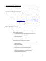
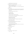
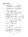
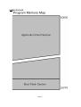
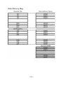
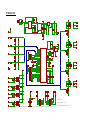
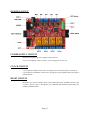
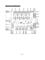
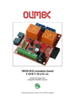
MOD-IO development board
user's manual
All boards produced by Olimex are ROHS compliant
Rev. C, March 2013
Copyright(c) 2011, OLIMEX Ltd, All rights reserved
Page 1
INTRODUCTION
MOD-IO is a small but powerful development board who let you control 4
optoisolated input and 4 relay outputs - with this features is possible to turn on
and off almost any electronic device at home. The board has UEXT_FEMALE
connector which allows you to communicate with a PC and UEXT_MALE
connector where you can connect other Olimex board with UEXT.
The MOD-IO project is fully open software and open hardware. The customer has
full access to the documentation of the board including schematics and board
design.
The main idea of MOD-IO chain connection is to extend:
- isolated relay outputs
- isolated digit inputs
- non isolated analog inputs
- non isolated digit inputs/outputs
using UEXT male/female connector. So the MCU interfaces (I2C, SPI, UART) from
all chain boards are connected in parallel.
Note that if you want to connect more than 1 MOD-IO board then on the interface
bus (I2C or UART or SPI) has to have only one Master device. The other devices
have to be Slaves.
For example: if UART interface is used - the master will send a string with Slave
address and command. All Slaves will listen UART bus through RXD line while
all Slave TXD lines are inputs. So when the address is recognized from the Slave
device, the one will answer as it will force TXD pin like output but immediately
after command answer is finished the Slave TXD pin must be initialized like input.
The same principle can be used for other interfaces (SPI or I2C).
BOARD FEATURES
–
Microcontroller: Atmega16L
–
AVRISP connector
–
JTAG connector
–
EXT connector
–
UEXT_MALE
–
UEXT_FEMALE
–
Clock circuit
–
User button
–
Reset circuit and button
–
Power Jack
–
Power-on led
–
Nine status leds
–
Four optocoupler isolated inputs
Page 2
–
Four Relays
–
PCB: FR-4, 1.5 mm (0,062"), solder mask, silkscreen component print
–
Dimensions: 100x80 mm (3.94x3.15")
Page 3
ELECTROSTATIC WARNING
The MOD-IO board is shipped in protective anti-static packaging. The board must
not be subject to high electrostatic potentials. General practice for working with
static sensitive devices should be applied when working with this board.
BOARD USE REQUIREMENTS
Cables:
Hardware:
Software:
The cable you will need depends on the programmer/debugger you
use. If you use AVR-PG1, or AVR-JTAG, you will need RS232 cable, if
you use AVR-PG2, you will need LPT cable, if you use AVR-USBJTAG, AVR-ISP500, AVR-ISP500-TINY, AVR-ISP500-ISO, AVR-ISPMK2 you will need 1.8 meter A-B USB cable.
One of Olimex programmers/debuggers – AVR-PG1, AVR-PG2,
AVR-ISP500, AVR-ISP500-TINY, AVR-ISP500-ISO, AVR-JTAG, AVRUSB-JTAG, AVR-ISP-MK2 or other compatible programming/debugging
tool.
Make sure to check if the above programmer/debugger is supported
by the IDE you are going to use.
AVR C Compiler
PROCESSOR FEATURES
MOD-IO use 8-bit AVR Microcontroller with 16K Bytes In-System Programmable
Flash, with these features:
–
High-performance, Low-power AVR® 8-bit Microcontroller
–
Advanced RISC Architecture
–
–
131 Powerful Instructions – Most Single-clock Cycle Execution
–
32 x 8 General Purpose Working Registers
–
Fully Static Operation
–
Up to 16 MIPS Throughput at 16 MHz
–
On-chip 2-cycle Multiplier
High Endurance Non-volatile Memory segments
–
16K Bytes of In-System Self-programmable Flash program memory
–
512 Bytes EEPROM
–
1K Byte Internal SRAM
–
Write/Erase Cycles: 10,000 Flash/100,000 EEPROM
–
Data retention: 20 years at 85°C/100 years at 25°C
–
Optional Boot Code Section with Independent Lock Bits
In-System Programming by On-chip Boot Program
True Read-While-Write Operation
Page 4
–
–
–
Programming Lock for Software Security
JTAG (IEEE std. 1149.1 Compliant) Interface
–
Boundary-scan Capabilities According to the JTAG Standard
–
Extensive On-chip Debug Support
–
Programming of Flash, EEPROM, Fuses, and Lock Bits through the JTAG
Interface
Peripheral Features
–
Two 8-bit Timer/Counters with Separate Prescalers and Compare Modes
–
One 16-bit Timer/Counter with Separate Prescaler, Compare Mode, and
Capture Mode
–
Real Time Counter with Separate Oscillator
–
Four PWM Channels
–
8-channel, 10-bit ADC
8 Single-ended Channels
7 Differential Channels in TQFP Package Only
2 Differential Channels with Programmable Gain at 1x, 10x, or 200x
–
–
–
Byte-oriented Two-wire Serial Interface
–
Programmable Serial USART
–
Master/Slave SPI Serial Interface
–
Programmable Watchdog Timer with Separate On-chip Oscillator
–
On-chip Analog Comparator
Special Microcontroller Features
–
Power-on Reset and Programmable Brown-out Detection
–
Internal Calibrated RC Oscillator
–
External and Internal Interrupt Sources
–
Six Sleep Modes: Idle, ADC Noise Reduction, Power-save, Power-down,
Standby and Extended Standby
I/O and Packages
–
–
Operating Voltages
–
–
2.7 - 5.5V
Speed Grades
–
–
32 Programmable I/O Lines
0 - 8 MHz
Power Consumption @ 1 MHz, 3V, and 25⋅C
–
Active: 1.1 mA
Page 5
–
Idle Mode: 0.35 mA
–
Power-down Mode: < 1 µA
Page 6
BLOCK DIAGRAM
Page 7
MEMORY MAP
Page 8
Page 9
SCHEMATIC
G1
DB104(SMD)
PWR_J
VR1(5V)
8
4
YDJ-1134
8-30 VDC
2
R1
3.3V
3
150k
C4
1uF/50v
220uF/35V
+5V
EN 5
VIN
LM1117IMPX-ADJ
SW 1
INV
N.C.
GND
7
FB
IN
100uH/SW68
RT 6
100n
110k
REL4
D9
RAS-05-15
1N4148/SMD
OUT
ADJ/GND
C5
R2
C3
green
O4
3.3V
VR2(3.3V)
L1
BD9001FSO-8
C1
4n7
C2
PWR_LED
red
R7
R4
D1
1N5819(smd)
R3
8.2K
REL4
R37
OUT4-3
OUT4-2
1K
C6
240R/1%
C7
R6
100n
390R/1%
10n
C9
C8
OUT4-1
R8
0R
AIN-1-1
100n
O1
1K
R35
T4
BC817
1K
GND
R36
R5
AIN-1-2
Fmax=50kHz
R19
AN1
100R
R20
C20
NA
33nF
10K
2K
green
O3
R9
100R
RST
AIN-1-3
TB2/3.5mm
R21
AN2
100R
R22
C21
NA
33nF
10K
O[1..4]
R23
AVRISP
AN3
100R
C22
R24
33nF
NA
2
1
4
3
6
5
8
7
10
9
RST
R11
AN4
100R
STAT
yellow
C23
R26
3.3V
330R
3.3V
TB2/3.5mm
RST
3.3V
1
4
3
6
5
8
7
10
(ADC7)PA7
31
(ADC6)PA6
AN3
32
(ADC5)PA5
AN4
O4
O3
O2
O1
33
(ADC4)PA4
34
(ADC3)PA3
35
(ADC2)PA2
36
(ADC1)PA1
37
(ADC0)PA0
Q2
REL3
RST
4
RESET
7
XTAL2
1
C12
33p
C13
Q1
8MHz/20pF
8
XTAL1
33p
(SCK)PB7
2
(MISO)PB6
1
(MOSI)PB5
44
(SS)PB4
43
(AIN1)PB3
42
(AIN0/INT2)PB2
41
(T1)PB1
40
(T0)PB0
26
(TOSC2)PC7
25
(TOSC1)PC6
24
PC5(TDI)
23
PC4(TDO)
22
PC3(TMS)
21
PC2(TCK)
20
PC1(SDA)
AREF
AVCC
AGND
TCK
TDO
TMS
TDI
9
O2
GND
R38
TDI
TDO
TMS
TCK
1K
R39
NA
10K
3.3V
29
100n
green
O2
27
C15
28
REL2
RAS-05-15
1N4148/SMD
100n
SDA
SCL
VCC2
19
PC0(SCL)
16
(OC2)PD7
2
15
(ICP)PD6
3
14
(OC1A)PD5
13
(OC1B)PD4
12
(INT1)PD3
11
(INT0)PD2
10
(TXD)PD1
9
(RXD)PD0
REL2
D7
R43
OUT2-3
OUT2-2
1K
VCC
VCC1
1
T3
BC817
3.3V
C14
3
OUT3-1
2
VCC
MCP130T
C11
OUT3-2
1K
RESET
OUT3-3
R40
U2
3.3V
32768Hz/6pF
JTAG
2
30
GND
33nF
NA
AIN-2-3
AN1
AN2
SCK
MISO
MOSI
#SS
LED
I2
I3
I4
BH10S
AIN-2-2
D8
REL3
1N4148/SMD
RAS-05-15
3.3V
T1107A(6x3.8x2.5mm)
R10
100n
AN[1..4]
3.3V
AIN-2-1
C10
5
OUT2-1
17
O3
38
R41
T2
BC817
1K
R42
10K
IN4-2
+
red
LED4 U6
R27
3.9k
I1
1
D5
1N4148/SMD
IN4-1
2
4
I1
3
+
H11A817SMD
3.9k
D4
1N4148/SMD
IN3-1
+
3.9k
D3
1N4148/SMD
4
2
3
I2
+
IN1-1
-
3.9k
100n
100n
100n
green
O1
39
REL1
D6
RAS-05-15
1N4148/SMD
1
2
H11A817SMD
OUT1-3
OUT1-2
OUT1-1
O4
2
REL1
R46
47K
I3
3.3V
3.3V
3.3V
3.3V
3.3V
R44
1K
3.3V
T1
BC817
R45
10K
4
I3
R32
R12
47K
3
4.7K
R13
I4
red
LED1 U3
D2
1N4148/SMD
18
ATMEGA16L
H11A817SMD
R33
C18
R30
-
IN1-2
C17
O[1..4]
1
1
IN2-1
GND2
C16
1K
red
LED2 U4
R31
GND1
I2
H11A817SMD
-
IN2-2
6
EXT
WF6S
red
LED3 U5
R29
I1
BUT
TXD
RXD
5
47K
-
IN3-2
4
R28
GND
6
4
3
I4
R34
47K
100n
NA
R15
R16
R17
R18
4.7K
NA
4.7K
4.7K
BUT
100R
C19
R14
BUT
T1107A(6x3.8x2.5mm)
UEXT_MALE
RXD1
SCL3
5
MISO
SCK7
9
BH10S
UEXT_FEMALE
2
TXD
SDA
MOSI
10 #SS
4
6
8
1
RXD
SCL3
5
MISO
SCK7
9
2
TXD
SDA
MOSI
10 #SS
4
6
8
IDC10S/PCB
This schematic is released under the Creative Commons Attribution-Share Alike 3.0 United States License.
MOD-IO_rev_A1
https://www.olimex.com
OLIMEX LTD, Plovdiv, Bulgaria, 2013
BOARD LAYOUT
POWER SUPPLY CIRCUIT
MOD-IO is typically power supplied with 8-30V DC.
Power consumption when all relays are working is about 310 mA.
CLOCK CIRCUIT
Crystal Quartz 8 MHz connected to Atmega16l pin 7 (XTAL2) and pin 8 (XTAL1).
Crystal Quartz 32.768kHz connected to Atmega16L pin 25 ((TOSC1)PC6) and pin 26
((TOSC2)PC7).
RESET CIRCUIT
MOD-IO reset circuit includes Reset scheme MCP130T (U2), AVRISP connector pin
5, JTAG connector pin 6, Atmega16L pin 4 (RESET), R9 (100Ohm), R10 (10k), C10
(100nF) and RST button.
Page 11
CONNECTOR DESCRIPTIONS
AVRISP
Pin #
Signal Name
1
MOSI
2
3.3V
3
NC
4
GND
5
RST
6
GND
7
SCK
8
GND
9
MISO
10
GND
Pin #
Signal Name
1
TCK
2
GND
3
TDO
4
3.3V
5
TMS
6
RST
7
3.3V
8
NC
9
TDI
10
GND
Pin #
Signal Name
1
PD7
2
PD6
3
PD5
4
PD4
5
3.3V
6
GND
JTAG
EXT
Page 12
UEXT_MALE
More info available here: https://www.olimex.com/Products/Modules/UEXT/
Pin #
Signal Name
1
NC
2
GND
3
RXD
4
TXD
5
SCL
6
SDA
7
MISO
8
MOSI
9
SCK
10
#SS
Pin #
Signal Name
1
NC
2
GND
3
RXD
4
TXD
5
SCL
6
SDA
7
MISO
8
MOSI
9
SCK
10
#SS
UEXT_FEMALE
Page 13
IN1, IN2 IN3, IN4
Please note that the opto-isolated inputs IN1, IN2, IN3, IN4 in earlier revisions were able to receive
signals in the 3V to 6V range. R27, R29, R31, R33 were 330R and R28, R30, R32, R34 were R4.7k.
We have now adjusted the values of the resistors in that part of the schematic in latest revisions to
allow higher voltage input in the 3.3V-24.0V range. R27, R29, R31, R33 are now R3.9k and R28, R30,
R32, R34 are now R47k
Pin #
Signal
1
-
2
+
IN1 connected to (T0)PB0 – signal I4
IN2 connected to (T1)PB1 – signal I3
IN2 connected to (AIN0/INT2)PB2 – signal I2
IN4 connected to (INT1)PD3 – signal I1
OUT1, OUT2, OUT3, OUT4
OUT1 connected to (ADC3)PA3 – signal name O4
OUT2 connected to (ADC2)PA2 – signal name O3
OUT3 connected to (ADC1)PA1 – signal name O2
OUT4 connected to (ADC0)PA0 – signal name O1
AIN-1
Please note that the analog inputs by default are as big as the input levels but you might change this.
Just calculate the needed resistors R19/R20 and R21/R22.
Pin #
Signal Name Connected to
1
3.3V
VCC
2
AN1
(ADC7)PA7
3
AN2
(ADC6)PA6
Page 14
AIN-2
Please note that the analog inputs by default are as big as the input levels but you might change this.
Just calculate (and mount/replace) the needed resistors R23/R24 and R25/R26.
Pin #
Signal Name Connected to
1
AN3
(ADC5)PA5
2
AN4
(ADC4)PA4
3
AGND
Analog GND
PWR_J
Pin #
Signal Name
1
Power Input
2
GND
Page 15
JUMPER DESCRIPTION
There are no jumpers on this board.
INPUT/OUTPUT
User button with name BUT – connected to Atmega16L pin 11 ((INT0)PD2).
Reset button with name RST – connected to Atmega16L pin 4 (RESET).
Status LED (yellow) with name STAT – connected via R11 (330 Ohm) to Atmega16l
pin 43 ((AIN1)PB3).
Status LED (red) with name LED1 – visualize input (IN1) state.
Status LED (red) with name LED2 – visualize input (IN2) state.
Status LED (red) with name LED3 – visualize input (IN3) state.
Status LED (red) with name LED4 – visualize input (IN4) state.
Status LED (green) with name O1 – visualize relay (REL1) state.
Status LED (green) with name O2 – visualize relay (REL2) state.
Status LED (green) with name O3 – visualize relay (REL3) state.
Status LED (green) with name O4 – visualize relay (REL4) state.
Power-on LED (red) with name PWR_LED – shows that +3.3V voltage is applied to
the board.
Page 16
MECHANICAL DIMENSIONS
Page 17
AVAILABLE DEMO SOFTWARE
There are two firmware available for MOD-IO: one is for RS232 control and the
other is for I2C control. They might be found at the web page of MOD-IO.
Direct download links:
–
–
MOD-IO I2C (newer) firmware C source and hex
MOD-IO RS232 (older) firmware C source and hex
Page 18
ORDER CODE
MOD-IO assembled and tested.
How to order?
You can order directly from our web shop or from any of our distributors. The list
of distributors might be found here: https://www.olimex.com/Distributors.
Check our web https://www.olimex.com for more info.
Revision history:
Board's revision:
Manual's revision:
Rev. A - create November 2009
Rev. B – edited September 2011
added more detailed INTRODUCTION and
MECHANICAL DIMENSIONS
Rev. C – edited March 2013
added new schematic, more information about
AIN and IN inputs; IN input voltage adjusted;
updated disclaimer and product support
Page 19
Disclaimer
© 2013 Olimex Ltd. Olimex®, logo and combinations thereof, are registered trademarks of Olimex Ltd.
Other product names may be trademarks of others and the rights belong to their respective owners.
The information in this document is provided in connection with Olimex products. No license,
express or implied or otherwise, to any intellectual property right is granted by this document or in
connection with the sale of Olimex products.
The Hardware project is released under the Creative Commons Attribution-Share Alike 3.0 United
States License. You may reproduce it for both your own personal use, and for commercial use. You
will have to provide a link to the original creator of the project https://www.olimex.com on any
documentation or website.
You may also modify the files, but you must then release them as well under the same terms. Credit
can be attributed through a link to the creator website: https://www.olimex.com
The software is released under GPL.
It is possible that the pictures in this manual differ from the latest revision of the board.
The product described in this document is subject to continuous development and improvements. All
particulars of the product and its use contained in this document are given by OLIMEX in good faith.
However all warranties implied or expressed including but not limited to implied warranties of
merchantability or fitness for purpose are excluded. This document is intended only to assist the
reader in the use of the product. OLIMEX Ltd. shall not be liable for any loss or damage arising from
the use of any information in this document or any error or omission in such information or any
incorrect use of the product.
This evaluation board/kit is intended for use for engineering development, demonstration, or
evaluation purposes only and is not considered by OLIMEX to be a finished end-product fit for
general consumer use. Persons handling the product must have electronics training and observe good
engineering practice standards. As such, the goods being provided are not intended to be complete in
terms of required design-, marketing-, and/or manufacturing-related protective considerations,
including product safety and environmental measures typically found in end products that
incorporate such semiconductor components or circuit boards.
Olimex currently deals with a variety of customers for products, and therefore our arrangement with
the user is not exclusive. Olimex assumes no liability for applications assistance, customer product
design, software performance, or infringement of patents or services described herein.
THERE IS NO WARRANTY FOR THE DESIGN MATERIALS AND THE COMPONENTS USED
TO CREATE MOD-IO. THEY ARE CONSIDERED SUITABLE ONLY FOR MOD-IO.
Page 20
For product support, hardware information and error reports mail to: [email protected]. Note that
we are primarily a hardware company and our software support is limited.
Please consider reading the paragraph below about the warranty of Olimex products.
Warranty and returns:
Our boards have lifetime warranty against manufacturing defects and components.
During development work it is not unlikely that you can burn your programmer or development
board. This is normal, we also do development work and we have damaged A LOT of programmers
and boards during our daily job so we know how it works. If our board/programmer has worked
fine then stopped, please check if you didn't apply over voltage by mistake, or shorted something in
your target board where the programmer was connected etc. Sometimes boards might get damaged
by ESD shock voltage or if you spill coffee on them during your work when they are powered.
Please note that warranty do not cover problems caused by unproper use, shorts, over-voltages, ESD
shock etc.
If the board has warranty label it should be not broken. Broken labels void the warranty, same
applies for boards modified by the customer, for instance soldering additional components or
removing components - such boards will be not be a subject of our warranty.
If you are positive that the problem is due to manufacturing defect or component you can return the
board back to us for inspection.
When we receive the board we will check and if the problem is caused due to our fault and we will
repair/replace the faulty hardware free of charge, otherwise we can quote price of the repair.
Note that all shippings back and forth have to be covered by the customer. Before you ship anything
back you need to ask for RMA. When you ship back please attach to it your shipping address, phone,
e-mail, RMA# and brief description of the problem. All boards should be sent back in antistatic
package and well packed to prevent damages during the transport.
Page 21