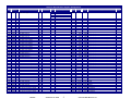
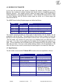
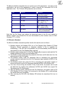
1
70 SERIES MEASUREMENT SYSTEM Modbus Manual September 30, 2009 ML0025 Document Revision C © 2009 by Bitronics, LLC TABLE OF CONTENTS 70 SERIES Firmware version ...................................................................................................................................... v 70 SERIES MANUAL SET............................................................................................................................................ vi CERTIFICATION ........................................................................................................................................................... vii INSTALLATION AND MAINTENANCE..................................................................................................................... vii WARRANTY AND ASSISTANCE .............................................................................................................................. vii COPYRIGHT NOTICE ................................................................................................................................................. viii TRADEMARKS............................................................................................................................................................. viii SAFETY SECTION......................................................................................................................................................... ix 1.0 MODBUS INTERFACE........................................................................................................................................... 1 1.1 Description............................................................................................................................................................ 1 1.2 Modbus Address.................................................................................................................................................. 1 1.3 Transaction Timing.............................................................................................................................................. 1 1.4 Data Format ......................................................................................................................................................... 2 1.4.1 70 Series IEDs Modbus Register Assignments (Configurable/SFC (Single Feeder Configurable))..................................................................................................................................................... 3 1.4.2 Modbus Calculation-Type Codes ......................................................................................................... 7 1.5 Configuration ........................................................................................................................................................ 8 1.5.1 Setting CT and VT Ratios........................................................................................................................... 8 1.5.2 Setting Current and Voltage Scale Factors ............................................................................................. 8 1.5.2a Scale Factor Voltage Measurement Example .................................................................................. 9 1.5.2b Scale Factor Current Measurement Example .................................................................................. 9 1.5.3 Resetting Energy and Demands and Triggering Recorders.................................................................10 1.5.4 Tag Register................................................................................................................................................10 1.5.5 VA Calculation Type Register...................................................................................................................10 1.6 Converting Data to Engineering Units .............................................................................................................11 1.7 Register Sets and Register Types.....................................................................................................................12 1.7.1 Time Sync Registers.......................................................................................................................................13 1.7.2 Best Clock Source Register...........................................................................................................................13 1.8 Health Check.......................................................................................................................................................13 1.9 Diagnostic Status LED.......................................................................................................................................15 1.10 Heartbeat State Counter .................................................................................................................................15 1.11 Meter ID Register .............................................................................................................................................15 2.0 MODBUS PROTOCOL ..........................................................................................................................................16 2.1 Introduction..........................................................................................................................................................16 2.2 MODBUS RTU Message Framing ...................................................................................................................16 2.3 MODBUS RTU Message Content....................................................................................................................16 2.4 MODBUS Function Codes ................................................................................................................................17 2.5 MODBUS Exception Codes ..............................................................................................................................17 2.6 Supported MODBUS Commands ....................................................................................................................17 2.6.1 Read Holding Registers (Function Code 03)..........................................................................................18 2.6.2 Preset Single Register (Function Code 06) ............................................................................................19 2.6.3 Preset Multiple Registers (Function Code 16)........................................................................................19 3.0 Modbus over Ethernet (TCP)..............................................................................................................................20 3.0.1 IP Addressing..............................................................................................................................................20 4.0 Modbus File Transfer ...........................................................................................................................................21 4.2 Bitronics Standard ..............................................................................................................................................22 4.2.1 Bitronics Compatibility Mode.....................................................................................................................23 ML0025 September 30, 2009 iii Copyright 2009 Bitronics LLC 4.3 Basic File Transfer .............................................................................................................................................23 4.4 File Transfer Configuration................................................................................................................................24 4.4.1 Modbus File System...................................................................................................................................24 4.4.2 Modbus Directory .......................................................................................................................................25 4.4.3 Downloads...................................................................................................................................................25 4.4.3a Manual File Select ...............................................................................................................................25 4.4.3b Automatic File Select ..........................................................................................................................25 4.4.4 Deleting a File .............................................................................................................................................26 4.4.4a Manual File Delete ..............................................................................................................................26 4.4.4b Automatic File Delete..........................................................................................................................26 4.5 File Transfer Configuration Modes...................................................................................................................26 4.5.1 Bitronics Mode.........................................................................................................................................27 4.5.2 Bitronics Mode – Auto-Delete Disabled ...............................................................................................27 4.5.3 Manual File Transfer Mode – Delete Disabled ..................................................................................27 4.5.4 Manual File Transfer Mode – Automatic Delete ................................................................................27 4.5.5 Manual File Transfer and Delete Mode ...................................................................................................28 Appendix A Bitronics Legacy Modbus Register Assignments ........................................................................29 Appendix B Bitronics Modbus Register Assignments.......................................................................................35 ML0025 September 30, 2009 iv Copyright 2009 Bitronics LLC 70 SERIES FIRMWARE VERSION The following table provides the most recent firmware and software versions. For best results, the Configurator version used should match with the firmware version. A complete list of firmware and software versions is provided on the 70 Series Utilities CD. Firmware Versions Description Bios Version DSP Firmware Host Firmware M870 Family Mx7x Product Release, New Hardware supported Dual Bus, Analog I/O 2.1/3.0* 1.210 2.050 2.1/3.0* " 2.1/3.0* 2.1/3.0* Mx7x Updated Release Mx7x Updated Release M87x Updated Release M87x Product Release, Fault Location, Adjustable Sample Rate M87x Product Release; Add Demand per phase for Watts ,VAr, & VA. Configurator & Biview improvements w/ modems. Change to Digital I/O default watchdog contact (Configurator setup; not firmware dependent). Support new version of hardware on P3x, P4x modules. M87x Product Release: Added 1mHz accuracy on M87x. Improved poll rate from 500ms to 100ms for a single P40 transducer inputs module (M87x). Fault distance configuration is changed. Time sync with respect to DNP master is changed from the DNP master jamming the time to asking the master what time to jam. Increased waveform recording limit from 999 post trigger for longer recording. M87x Product Release, IEC61850 & SNTP; Avg 3-Ph Amps and Avg 3-Ph Volts ML0025 Utilities CD Release Date 2.31 2.43 03/24/06 2.060 2.32 2.44 04/14/06 1.240 1.240 2.120 2.150 2.39 2.41 2.50 2.52 10/01/06 12/18/06 3.40 1.30 2.170 2.43 2.56 12/21/07 3.40 1.30 2.18 3.00A 2.57 10/17/08 3.40 1.31 2.19 3.40 1.30 3.01.0 September 30, 2009 v Configurator 3.02 3.01 2.58 3.01 09/30/2009 1/30/09 Copyright 2009 Bitronics LLC Firmware Versions Bios Version Description M87x Product Release: Added 1mHz accuracy on M87x. Improved poll rate from 500ms to 100ms for a single P40 transducer inputs module (M87x). Fault distance configuration is changed. Time sync with respect to DNP master is changed from the DNP master jamming the time to asking the master what time to jam. Increased waveform recording limit from 999 post trigger for longer recording. 3.40 DSP Firmware Host Firmware Configurator Utilities CD 1.31 3.02 3.02 3.02 Release Date 09/30/2009 * H10/H11 70 SERIES MANUAL SET ML0021 ML0032 ML0022 ML0024 ML0025 ML0026 ML0027 ML0033 ML0034 ML0025 M87X User Manual M57X User Manual 70 SERIES UCA® Object Model 70 SERIES Modbus Plus Module & Protocol 70 SERIES Modbus Protocol 70 SERIES DNP3 Protocol M870D Remote Display Manual M570Dx Remote Display Manual 70 Series IEC61850® Protocol Manual September 30, 2009 vi Copyright 2009 Bitronics LLC CERTIFICATION Bitronics LLC certifies that the calibration of our products is based on measurements using equipment whose calibration is traceable to the United States National Institute of Standards Technology (NIST). INSTALLATION AND MAINTENANCE Bitronics LLC products are designed for ease of installation and maintenance. As with any product of this nature, installation and maintenance can present electrical hazards and should be performed only by properly trained and qualified personnel. If the equipment is used in a manner not specified by Bitronics LLC, the protection provided by the equipment may be impaired. WARRANTY AND ASSISTANCE This product is warranted against defects in materials and workmanship for a period of thirty-six (36) months from the date of their original shipment from the factory. Products repaired at the factory are likewise warranted for eighteen (18) months from the date the repaired product is shipped, or for the remainder of the product's original warranty, whichever is greater. Obligation under this warranty is limited to repairing or replacing, at our designated facility, any part or parts that our examination shows to be defective. Warranties only apply to products subject to normal use and service. There are no warranties, obligations, liabilities for consequential damages, or other liabilities on the part of Bitronics LLC except this warranty covering the repair of defective materials. The warranties of merchantability and fitness for a particular purpose are expressly excluded. For assistance, contact Bitronics LLC at: Telephone: Fax: Email: Website: 610.997.5100 610.997.5450 [email protected] www.novatech.com/bitronics Shipping: 261 Brodhead Road Bethlehem, PA 18017-8698 USA ML0025 September 30, 2009 vii Copyright 2009 Bitronics LLC COPYRIGHT NOTICE This manual is copyrighted and all rights are reserved. The distribution and sale of this manual is intended for the use of the original purchaser or his agents. This document may not, in whole or part, be copied, photocopied, reproduced, translated or reduced to any electronic medium or machine-readable form without prior consent of Bitronics LLC, except for use by the original purchaser. The product described by this manual contains hardware and software that is protected by copyrights owned by one or more of the following entities: Bitronics LLC, 261 Brodhead Road, Bethlehem, PA 18017; VentureCom, Inc., Five Cambridge Center, Cambridge, MA 02142; SISCO, Inc., 6605 192 Mile Road, Sterling Heights, MI 48314-1408; General Software, Inc., Box 2571, Redmond, WA 98073; Schneider Automation, Inc., One High Street, North Andover, MA 01845; Triangle MicroWorks, Inc., 2213 Middlefield Court, Raleigh, NC 27615 Greenleaf Software Inc., Brandywine Place, Suite 100, 710 East Park Blvd, Plano, TX 75074 TRADEMARKS The following are trademarks or registered trademarks of Bitronics, LLC: The Bitronics logo Bitronics PowerPlex Triplex Triple-II MultiComm PowerServe SubCycle Technology SubCycleStuf The following are trademarks or registered trademarks of AREVA T&D Inc.: AREVA T&D the AREVA logo MiCOM The following are trademarks or registered trademarks of the DNP User's Group: DNP DNP3 The following are trademarks or registered trademarks of the Electric Power Research Institute (EPRI): UCA UCA2 The following are trademarks or registered trademarks of Schneider Automation, Inc.: MODSOFT Modicon Modbus Plus Modbus Compact 984 PLC The following are trademarks or registered trademarks of VentureCom, Inc.: Phar Lap the Phar Lap logo The following are trademarks or registered trademarks of Systems Integration Specialists Company, Inc. (SISCO): SISCO MMS-EASE Lite AX-S4MMS The following are trademarks or registered trademarks of General Software, Inc.: General Software the GS logo EMBEDDED BIOS Embedded DOS The following are trademarks or registered trademarks of the PCI Industrial Computer Manufacturers Group: CompactPCI PICMG the CompactPCI logo the PICMG logo ML0025 September 30, 2009 viii Copyright 2009 Bitronics LLC SAFETY SECTION Please refer to the M87x and M57x User Manuals, ML0021 and ML0032 respectively, for information regarding safety, installation, commissioning and decommissioning. ML0025 September 30, 2009 ix Copyright 2009 Bitronics LLC 1.0 MODBUS INTERFACE 1.1 Description The 70 Series IEDs support the Modbus protocol on two or three of the serial ports (P2 and P3 for M57x, P2-P4 on M87x). These ports can be configured for RS-232 or RS-485. All of these ports can be used simultaneously. Refer to the M87X or M57X User Manuals for hardware details. The Modbus network is a "MASTER" to "SLAVE" network, that is to say, one node asks a question and a second node answers. A NODE is a Modbus device (PLC, Computer, M871, etc.) that is connected to the network. Each SLAVE NODE has an ADDRESS in the range of 1 to 247; it is this address that allows a MASTER to selectively request data from any other device. Address 0 is a BROADCAST ADDRESS that can be used with certain MODBUS functions to allow the MASTER to address all SLAVE NODES at one time. The 70 Series IEDs do not respond to BROADCAST messages. The Modbus implementation in the 70 Series IEDs conforms to all standard Modbus specifications and capabilities, such as maximum nodes, distance, signal sensitivity, etc. The 70 Series IEDs are classified as SLAVE DEVICES in the Modbus structure. The data items that are available from the instrument can be obtained via the Modbus Network by issuing a READ HOLDING REGISTERS command from the requesting node. 1.2 Modbus Address Ports 2 & 3 in the M57x or 2, 3, and 4 in the M87x can be set up to be RS-232 or RS-485 (P1 is RS-232 only, and does not support Modbus), and support baud rates up to 38400. Setting the address and configuring the Serial Ports can be accomplished by running the 70 Series Configurator. The default configuration for the serial ports is: Serial Port Default Settings Port Protocol Parity Baud IED Address Physical Media P1 Zmodem/Display/Log None 9600 P2 DNP 3.0 None 9600 1 RS-232 P3 Modbus Even 9600 1 RS-232 P4 Zmodem/Display/Log None 9600 RS-232 RS-232 1.3 Transaction Timing The instrument completes a set of calculations approximately every cycle (16.67ms @60Hz) and calculations for volt and amp measurements every quarter cycle (4.167ms @60Hz). The HOST CPU processor service the Modbus ports by interrupts received from the corresponding serial ports. Incoming messages are parsed and responded to in approximately 2 ms. ML0025 September 30, 2009 1 Copyright 2009 Bitronics LLC 1.4 Data Format The 70 Series IEDs contain a set of holding registers (4XXXX) into which the instrument places values that correspond to the measurements the instrument is making. These holding registers can be read by any other device on the network using a READ HOLDING REGISTER (Function Code 3). When using HOLDING REGISTER DATA, the Health Check Register should always be read and checked before interpreting data, since some failure modes will cause erroneous data to be presented (See Section 1.8). For conversion of the register data into ENGINEERING UNITS, please refer to Section 1.6. For specifics concerning the correct command and its implementation, users are directed to the M87X and M57x User Manuals for the specific device that will request the data. Listed in section 1.4.1 are the register assignments for the 70 SERIES IEDs when using the Configurable or Single Feeder Configurable (SFC) selection (used for M571 and M871). Appendix A provides the Legacy or Bitronics Legacy Fixed (BiLF) register set. NOTE: The 70 Series IEDs have a total of up to 6 different register sets (depending upon Configurator and firmware versions). A summary of the assignments for each of these six register sets is provided in Appendix B. Please refer to the 70 Series Configurator Modbus Register tab and click on the various options in the “Register Set” section to see register assignment details. For Configurator versions 2.27 or higher, the Register Sets on the left side of the box in the Modbus Register Screen are all fixed sets whereas the ones on the right side of the box are all configurable to varying degrees (some have a fixed portion followed by a section where the user can select any of the measurements available in the 70 Series IEDs). Note also that unless otherwise specified, all points are READ ONLY. ML0025 September 30, 2009 2 Copyright 2009 Bitronics LLC 1.4.1 70 Series IEDs Modbus Register Assignments (Configurable/SFC (Single Feeder Configurable)) 70 Series IEDs Modbus Register Assignments Code Modbus Address 3 40001 Health 0 T1 3 40002 Health 1 T1 3 3 3 3 3 3 3 3 3 3 3 3 3 3 3 Amps A Amps B Amps C Amps N Amps Residual Volts A Volts B Volts C Volts N Volts AB Volts BC Volts CA Volts A Bus2 Volts B Bus2 Volts C Bus2 T2 T2 T2 T3 T3 T4 T4 T4 T4 T4 T4 T4 T4 T4 T4 40003 40004 40005 40006 40007 40008 40009 40010 40011 40012 40013 40014 40015 40016 40017 Contents ML0025 Data Scale Ind Bit-0 Bit-1 Bit-2 Bit-3 Bit-4 Bit-5 Bit-6 Bit-7 Bit-8 Bit-9 Bit-10 Bit-11 Bit-12 Bit-13 Bit-14 Bit-15 Bit-0 Bit-1 Bit-2 Bit-3 Bit-4 Bit-5 Bit-6 Bit-7 Bit-8 Bit-9 Bit-10 Bit-11 Bit-12 Bit-13 Bit-14 Bit-15 Amp Scale Amp Scale Amp Scale Amp Scale Amp Scale Volt Scale Volt Scale Volt Scale Volt Scale Volt Scale Volt Scale Volt Scale Volt Scale Volt Scale Volt Scale Values/Dependencies Type DSP Gain Cal Error Data DSP Offset Cal Error SIM Gain Cal Error SIM Offset Cal Error SIM Phase Cal error SIM Ratio Csum Error User Ratio Csum Error User Gain Csum Error User Phase Csum Error DSP Board ID Csum Error SIM Board ID Csum Error User TDD Csum Error DSP Integrity Csum Error DSP Stack Overflow CT\VT Scaling Error Protocol Config Error Reserved Data Reserved Reserved Reserved Reserved Reserved Reserved Reserved Reserved Reserved Reserved Reserved Reserved Reserved Reserved Reserved Data Data Data Data Data Data Data Data Data Data Data Data Data Data Data September 30, 2009 3 Min Max Step 0-Norm 1-Fail 1 0-Norm 1-Fail 1 0 0 0 0 0 0 0 0 0 0 0 0 0 0 0 32767 32767 32767 32767 32767 32767 32767 32767 32767 32767 32767 32767 32767 32767 32767 ((1/32768) *10*Amp Scale) ((1/32768) *10*Amp Scale) ((1/32768) *10*Amp Scale) ((1/32768) *15*Amp Scale) ((1/32768) *15*Amp Scale) ((1/32768) *150*Volt Scale) ((1/32768) *150*Volt Scale) ((1/32768) *150*Volt Scale) ((1/32768) *150*Volt Scale) ((1/32768) *150*Volt Scale) ((1/32768) *150*Volt Scale) ((1/32768) *150*Volt Scale) ((1/32768) *150*Volt Scale) ((1/32768) *150*Volt Scale) ((1/32768) *150*Volt Scale) Copyright 2009 Bitronics LLC Pass A A A A A V V V V V V V V V V 70 Series IEDs Modbus Register Assignments Code 3 3 3 3 3 Modbus Address 40018 40019 40020 40021 40022 Contents Data Scale Values/Dependencies Type Min Max Step * Data Data Data Data Data 0 0 0 0 -32768 32767 32767 32767 32767 32767 * Data -32768 32767 ((1/32768) *1500*Amp Scale * Volt Scale) W * Data -32768 32767 ((1/32768) *1500*Amp Scale * Volt Scale) W * Data -32768 32767 ((1/32768) *4500*Amp Scale * Volt Scale) W * Data -32768 32767 ((1/32768) *1500*Amp Scale * Volt Scale) vars * Data -32768 32767 ((1/32768) *1500*Amp Scale * Volt Scale) vars * Data -32768 32767 ((1/32768) *1500*Amp Scale * Volt Scale) vars * Data -32768 32767 ((1/32768) *4500*Amp Scale * Volt Scale) vars * Data 0 32767 ((1/32768) *1500*Amp Scale * Volt Scale) VAs * Data 0 32767 ((1/32768) *1500*Amp Scale * Volt Scale) VAs * Data 0 32767 ((1/32768) *1500*Amp Scale * Volt Scale) VAs * Data 0 32767 ((1/32768) *4500*Amp Scale * Volt Scale) VAs Volts N Bus2 Volts AB Bus2 Volts BC Bus2 Volts CA Bus2 Watts A T4 T4 T4 T4 T5 3 40023 Watts B T5 3 40024 Watts C T5 3 40025 Watts Total T6 3 40026 VARs A T5 3 40027 VARs B T5 3 40028 VARs C T5 3 40029 VARs Total T6 3 40030 VAs A T5 3 40031 VAs B T5 3 40032 VAs C T5 3 40033 VAs Total Geometric T6 3 3 3 3 3 3 3 3 3 3 3 3 3 3 3 Power Factor A Power Factor B Power Factor C Power Factor Total Geometric Frequency Volts A Frequency Volts B Frequency Volts C Frequency Volts A Bus2 Frequency Volts B Bus2 Frequency Volts C Bus2 System Frequency Phase Angle Volts A Bus1-Bus2 Phase Angle Volts B Bus1-Bus2 Phase Angle Volts C Bus1-Bus2 Phase Angle Amps A Harmonic 1 Phase Angle Amps B Harmonic 1 Phase Angle Amps C Harmonic 1 Phase Angle Volts A Harmonic 1 Phase Angle Volts B Harmonic 1 Phase Angle Volts C Harmonic 1 T7 T7 T7 T7 T8 T8 T8 T8 T8 T8 T8 T9 T9 T9 T9 Data Data Data Data Data Data Data Data Data Data Data Data Data Data Data -1000 -1000 -1000 -1000 2000 2000 2000 2000 2000 2000 2000 -1800 -1800 -1800 -1800 1000 1000 1000 1000 8000 8000 8000 8000 8000 8000 8000 1800 1800 1800 1800 T9 Data -1800 1800 0.1 Degrees T9 Data -1800 1800 0.1 Degrees T9 T9 T9 Data Data Data -1800 -1800 -1800 1800 0.1 Degrees 1800 0.1 Degrees 1800 0.1 Degrees 40034 40035 40036 40037 40038 40039 40040 40041 40042 40043 40044 40045 40046 40047 40048 3 40049 3 40050 3 40051 3 40052 3 40053 ML0025 Volt Scale Volt Scale Volt Scale Volt Scale Amp Scale Volt Scale Amp Scale Volt Scale Amp Scale Volt Scale Amp Scale Volt Scale Amp Scale Volt Scale Amp Scale Volt Scale Amp Scale Volt Scale Amp Scale Volt Scale Amp Scale Volt Scale Amp Scale Volt Scale Amp Scale Volt Scale Amp Scale Volt Scale Ind September 30, 2009 4 ((1/32768) *150*Volt Scale) V ((1/32768) *150*Volt Scale) V ((1/32768) *150*Volt Scale) V ((1/32768) *150*Volt Scale) V ((1/32768) *1500*Amp Scale * Volt Scale) W 0.001 0.001 0.001 0.001 0.01 Hz 0.01 Hz 0.01 Hz 0.01 Hz 0.01 Hz 0.01 Hz 0.01 Hz 0.1 Degrees 0.1 Degrees 0.1 Degrees 0.1 Degrees Copyright 2009 Bitronics LLC Pass 70 Series IEDs Modbus Register Assignments Code 3,6,16 Modbus Address 40054 Contents VA/PF Calc. Type T1 3 3,6,16 3,6,16 3,6,16 3,6,16 3,6,16 3,6,16 3,6,16 3,6,16 3,6,16 3,6,16 3,6,16 3,6,16 3,6,16 3,6,16 3,6,16 3,6,16 3,6,16 3,6,16 3,6,16 3,6,16 3,6,16 3,6,16 3,6,16 3,6,16 3,6,16 3,6,16 3,6,16 3,6,16 3,6,16 3,6,16 3,6,16 3,6,16 3,6,16 3,6,16 3,6,16 3,6,16 3,6,16 3,6,16 3,6,16 3,6,16 3,6,16 3,6,16 3,6,16 3,6,16 40055 40056 40057 40058 40059 40060 40061 40062 40063 40064 40065 40066 40067 40068 40069 40070 40071 40072 40073 40074 40075 40076 40077 40078 40079 40080 40081 40082 40083 40084 40085 40086 40087 40088 40089 40090 40091 40092 40093 40094 40095 40096 40097 40098 40099 Meter Type Volt Scale Factor Volt Scale Factor Divisor Amp Scale Factor Amp Scale Factor Divisor Xfmr Ratio Volts A Xfmr Ratio Divisor Volts A Xfmr Ratio Volts B Xfmr Ratio Divisor Volts B Xfmr Ratio Volts C Xfmr Ratio Divisor Volts C Xfmr Ratio Volts N Xfmr Ratio Divisor Volts N Xfmr Ratio Volts A Bus2 Xfmr Ratio Divisor Volts A Bus2 Xfmr Ratio Volts B Bus2 Xfmr Ratio Divisor Volts B Bus2 Xfmr Ratio Volts C Bus2 Xfmr Ratio Divisor Volts C Bus2 Xfmr Ratio Volts N Bus2 Xfmr Ratio Divisor Volts N Bus2 Xfmr Ratio Amps A Xfmr Ratio Divisor Amps A Xfmr Ratio Amps B Xfmr Ratio Divisor Amps B Xfmr Ratio Amps C Xfmr Ratio Divisor Amps C Xfmr Ratio Amps N Xfmr Ratio Divisor Amps N User Gain Volts A User Gain Volts B User Gain Volts C User Gain Volts N User Gain Volts A Bus2 User Gain Volts B Bus2 User Gain Volts C Bus2 User Gain Volts N Bus2 User Gain Amps A User Gain Amps B User Gain Amps C User Gain Amps N User Phase Correction Volts A User Phase Correction Volts B User Phase Correction Volts C User Phase Correction Volts N T1 T10 T11 T10 T11 T10 T11 T10 T11 T10 T11 T10 T11 T10 T11 T10 T11 T10 T11 T10 T11 T10 T11 T10 T11 T10 T11 T10 T11 T12 T12 T12 T12 T12 T12 T12 T12 T12 T12 T12 T12 T8 T8 T8 T8 ML0025 Data Scale Ind 1 2 3 4 402 Values/Dependencies Arithmetic Geometric 3 Element (L-N) 2 Element (L-L) 70 Series Register Set September 30, 2009 5 Type Min Max Setting 1 Data Setting Setting Setting Setting Setting Setting Setting Setting Setting Setting Setting Setting Setting Setting Setting Setting Setting Setting Setting Setting Setting Setting Setting Setting Setting Setting Setting Setting Setting Setting Setting Setting Setting Setting Setting Setting Setting Setting Setting Setting Setting Setting Setting Setting 402 1000 1 1000 1 1000 1 1000 1 1000 1 1000 1 1000 1 1000 1 1000 1 1000 1 1000 1 1000 1 1000 1 1000 1 -32768 -32768 -32768 -32768 -32768 -32768 -32768 -32768 -32768 -32768 -32768 -32768 -18000 -18000 -18000 -18000 Step 41 400 9999 1000 9999 1000 9999 1000 9999 1000 9999 1000 9999 1000 9999 1000 9999 1000 9999 1000 9999 1000 9999 1000 9999 1000 9999 1000 9999 1000 32767 32767 32767 32767 32767 32767 32767 32767 32767 32767 32767 32767 18000 18000 18000 18000 0 1 Multiply by 10 (valid values are 1,10,100,1000) 1 Multiply by 10 (valid values are 1,10,100,1000) 1 Multiply by 10 (valid values are 1,10,100,1000) 1 Multiply by 10 (valid values are 1,10,100,1000) 1 Multiply by 10 (valid values are 1,10,100,1000) 1 Multiply by 10 (valid values are 1,10,100,1000) 1 Multiply by 10 (valid values are 1,10,100,1000) 1 Multiply by 10 (valid values are 1,10,100,1000) 1 Multiply by 10 (valid values are 1,10,100,1000) 1 Multiply by 10 (valid values are 1,10,100,1000) 1 Multiply by 10 (valid values are 1,10,100,1000) 1 Multiply by 10 (valid values are 1,10,100,1000) 1 Multiply by 10 (valid values are 1,10,100,1000) 1 Multiply by 10 (valid values are 1,10,100,1000) 1/16384 1/16384 1/16384 1/16384 1/16384 1/16384 1/16384 1/16384 1/16384 1/16384 1/16384 1/16384 0.01 Degrees 0.01 Degrees 0.01 Degrees 0.01 Degrees Copyright 2009 Bitronics LLC Pass 70 Series IEDs Modbus Register Assignments Code 3,6,16 Modbus Address 40100 3,6,16 40101 3,6,16 40102 3,6,16 40103 3,6,16 3,6,16 3,6,16 3,6,16 40104 40105 40106 40107 Contents User Phase Correction Volts A Bus2 User Phase Correction Volts B Bus2 User Phase Correction Volts C Bus2 User Phase Correction Volts N Bus2 User Phase Correction Amps A User Phase Correction Amps B User Phase Correction Amps C User Phase Correction Amps N ML0025 Data Scale Ind Values/Dependencies Type Min Max Step T8 Setting -18000 18000 0.01 Degrees T8 Setting -18000 18000 0.01 Degrees T8 Setting -18000 18000 0.01 Degrees T8 Setting -18000 18000 0.01 Degrees T8 T8 T8 T8 Setting Setting Setting Setting -18000 -18000 -18000 -18000 18000 18000 18000 18000 September 30, 2009 6 0.01 Degrees 0.01 Degrees 0.01 Degrees 0.01 Degrees Copyright 2009 Bitronics LLC Pass 1.4.2 Modbus Calculation-Type Codes Type T1 T2 T3 T4 T5 T6 T7 T8 T9 T10 T11 T12 T13 T14 T15 T16 T17 T18 T19 T20 T21 T22 ML0025 Value / Bit Mask Description Unsigned 16-Bit Integer Signed 16-Bit Integer - 2's Complement - Saturation 10 Float Value = ( (Integer Value) / 32768) * Scale * 10) Example: 5.0 A stored as 16384 when Amp Scale = 1:1 Signed 16-Bit Integer - 2's Complement - Saturation 15 Float Value = ( (Integer Value) / 32768) * Scale * 15) Example: 150 A stored as 16384 when Amp Scale = 20:1 Signed 16-Bit Integer - 2's Complement - Saturation 150 Float Value = ( (Integer Value) / 32768) * Scale * 150) Example: 119.998 V stored as 26214 when Volt Scale = 1:1 Signed 16-Bit Integer - 2's Complement - Saturation 1500 Float Value = ( (Integer Value) / 32768) * Scale * 1500) Example: -750.0 W stored as -16384 when Volt Scale = 1:1, Amp Scale 1:1 Signed 16-Bit Integer - 2's Complement - Saturation 4500 Float Value = ( (Integer Value) / 32768) * Scale * 4500) Example: -90.0 kW stored as -8192 when Volt Scale = 20:1, Amp Scale 4:1 Signed 16-Bit Integer - 2's Complement - 3 Decimal Places Example: -12.345 stored as -12345 Signed 16-Bit Integer - 2's Complement - 2 Decimal Places Example: 123.45 stored as 12345 Signed 16-Bit Integer - 2's Complement -1 Decimal Place Example: -1234.5 stored as -12345 Unsigned 16-Bit Integer - Normalized Ratio ratio = (Normalized Ratio / Ratio Divisor) Example : 1.234, 12.34, 123.4, and 1234 are all stored as 1234 Unsigned 16-Bit Integer - Ratio Divisor ratio = (Normalized Ratio / Ratio Divisor); valid Ratio Divisors are 1,10,100,1000 Example: X.XXX stored as 1000, XX.XX stored as 100, XXX.X stored as 10 Signed 16-Bit - 2's Complement - Saturation 2 Gain Value = Integer Value /16384) Example: -0.250 stored as -4096 Unsigned 16-Bit Integer - 12 Bit Offset Binary - Saturation 10 Float Value =( (Integer Value - 2047) / (2048) ) * Scale * 10 Example: 5.0 A stored as 3071 when Amp Scale 1:1 Unsigned 16-Bit Integer - 12 Bit Offset Binary - Saturation 150 Float Value =( (Integer Value - 2047) / (2048) ) * Scale * 150 Example: 119.97 V stored as 3685 when Volt Scale 1:1 Unsigned 16-Bit Integer - 12 Bit Offset Binary - Saturation 1000 Float Value =( (Integer Value - 2047) / (2048) ) * Scale * 1000 Example: -500 W stored as 1023 when Volt Scale = 1:1, Amp Scale = 1:1 Unsigned 16-Bit Integer - 12 Bit Offset Binary - Saturation 3000 Float Value =( (Integer Value - 2047) / (2048) ) * Scale * 3000 Example: 349.10 kW stored as 3040 when Volt Scale = 6:1, Amp Scale = 40:1 Unsigned 16-Bit Integer - 12 Bit Offset Binary - Saturation 15 Float Value =( (Integer Value - 2047) / (2048) ) * Scale * 15 Example: 11.79 A stored as 2369 when Amp Scale 5:1 Unsigned 16-Bit Integer - 12 Bit Offset Binary -1 Decimal Place Float Value = ( (Integer Value - 2047) / (10) ) Example: 121.4 degrees stored as 3261 Unsigned 16-Bit Integer - 12 Bit Offset Binary -3 Decimal Place Float Value = ( (Integer Value - 2047) / (1000) ) Example: 0.978 Power Factor stored as 3025 Unsigned 16-Bit Integer - Bit Control/Status 0' - stored as zero; '1' - stored as 65536 Unsigned 16-Bit Integer - 3 Decimal Places Example: 54.321 stored as 54321 Bit Example: 1-bit is set, 0-bit is clear September 30, 2009 7 Copyright 2009 Bitronics LLC 1.5 Configuration 1.5.1 Setting CT and VT Ratios The 70 Series IEDs are capable of internally storing and recalling CT and VT ratios. The CT and VT ratios are written to registers 40060 through 40083 over the Modbus communication port, and are stored in non-volatile memory on the CT/VT Module. Each ratio is stored in two registers, one for the Normalized Ratio and the other for the Ratio Divisor. Allowable constants for the normalized ratios are 1000 to 9999. The Ratio Divisors may be 1, 10, 100, or 1000 only. The number stored will be the high side rating of the CT Ratio or VT Ratio. Both a 500:5 ratio CT and a 100:1 CT will have a value of 100 stored. For example, to calculate a CT and VT ratio for Phase A from the data stored in the M871, use the following equation: Phase A CT Value (40076 ) Phase A CT RatioDivisor (40077 ) Phase A PT Value (40060 ) Phase A PT RatioDivisor (40061) Phase A CT RATIO Phase A PT RATIO The 70 Series IEDs calculate all measured quantities in PRIMARY UNITS, unlike other Bitronics instruments (MultiComm and PowerPlex). The CT and VT ratio information (registers 40060 through 40083) is used to calculate these primary values. To force the 70 Series IED to report in secondary units, set the Scale Factor = to the CT or VT ratio, as appropriate. Note: The Full Scale Integer Value of current and voltage reported by the 70 Series IEDs over Modbus can be changed, see Section 1.5.2. In the event of a CT/VT Ratio Checksum Failure, the value in the Normalized CT Ratio and Normalized VT Ratio registers default to 1000, and the value in the CT Ratio Divisor and VT Ratio Divisor default to 1000. This results in a 1:1 CT Ratio and 1:1 VT Ratio. WARNING – TO PRESERVE SYSTEM PERFORMANCE, ONLY WRITE TO RATIO REGISTERS WHEN THE RATIOS NEED TO BE CHANGED. 1.5.2 Setting Current and Voltage Scale Factors As detailed in Section 1.6, the data in the 70 Series IED Modbus registers is in NORMALIZED 2'S COMPLEMENT format. Measurements presented in this format do not have as much resolution as the 70 Series IED internal floating register values. Because of the wide dynamic range of the 70 Series IED inputs, the default full-scale integer representation of measurement values is a compromise that has been selected to accommodate typical system signal levels, while giving reasonable resolution. The maximum (or full scale) integer value that can be reported corresponds to some particular level of Amperes, Volts, Watts, etc. The maximum full scale integer value of Amperes and Volts in the NORMALIZED 2'S COMPLEMENT format can be changed by means of the Current Scale Factor and Voltage Scale Factor (ISCALE FACTOR and VSCALE FACTOR), which are modified by writing to the Normalized Scale Factor and Scale Factor Divisor (40056 to 40059) registers. These ML0025 September 30, 2009 8 Copyright 2009 Bitronics LLC Current Scale Factor and Voltage Scale Factor values are multipliers of the Default Full Scale values. To convert values reported in Modbus registers to engineering units, refer to Section 1.6. The default full-scale values for quantities are: Quantity Default Full Scale Phase Current Neutral Current Voltages Per-Phase Power (Watt, VAR, VA) Total Power (Watt, VAR, VA) 10 15 150 1500 4500 Normalized Current ScaleFactor (40058 ) Current ScaleFactor Divisor (40059 ) NormalizedVoltageScaleFactor (40056 ) VoltageScaleFactor Divisor (40057 ) I SCALE FACTOR VSCALE FACTOR The Current and Voltage Scale Factors are written to registers 40056 through 40059 and are stored in non-volatile memory on the 70 SERIES IED's Host CPU Board. Each Scale Factor is stored in two registers, one for the Normalized Scale Factor, and the other for the Scale Factor Divisor. Allowable constants for Normalized Scale Factors are 1000 to 9999. The Scale Factor Divisors may be 1, 10, 100, or 1000 only. 1.5.2a Scale Factor Voltage Measurement Example For example, the default full-scale value of voltage (registers 40008 to 40021) is 150V, the default value of the Normalized Voltage Scale Factor (40056) is 1000, and the default value of the Voltage Scale Factor Divisor (40057) is 1000. Assume a system with a 1:1 VT Ratio. If it is desired to change the full-scale representation of volts to 300V (to accommodate a 208V input, for instance), change the value of the Normalized Voltage Scale Factor (40056) to 2000. VOLTAGE Phase A B Value 2000 150 300V 32768 1000 Note that since VSCALE FACTOR = 2, the values represented by the power quantity registers will also be doubled. Note that the full-scale representation of all the Voltage measurements will also change. The scaling for Power quantities cannot be set independently and will be the product of the Voltage and Current Scale Factors. 1.5.2b Scale Factor Current Measurement Example Consider a system with a 2000:5 (400:1) CT, on which it is desired to measure the Phase A amperes. The Normalized CT Ratio (40060) would be set to 4000, the CT Ratio Divisor (40061) to 10. With the default settings for the Current Scale Factor, the maximum register value of "32767" would yield: ML0025 September 30, 2009 9 Copyright 2009 Bitronics LLC AMPEREsPhase A Value ( 32767 ) 1000 10 10A 32768 1000 In other words, the integer value for Amperes would be at a maximum with only 10A flowing through the system primary conductors. To compensate for this, set the ISCALE FACTOR equal to the CTRATIO. The Normalized Current Scale Factor (40058) would be set to 4000, and the Current Scale Factor Divisor (40059) to 10. If the maximum value of "32767" is returned in register 40003, it is converted to Amperes as follows: AMPEREsPhase A Value 32767 4000 10 I SCALE FACTOR 10 4000A 32768 32768 10 If it is known that the maximum current on the circuit is not this high, and it is desired to set the full scale representation to 1200A for added resolution, the Normalized Current Scale Factor (40058) could be set to 1200, and the Current Scale Factor Divisor (40059) to 10. The maximum value returned (32767) would then be equal to: AMPEREsPhase A Value ( 32767 ) 1200 10 1200A 32768 10 1.5.3 Resetting Energy and Demands and Triggering Recorders The Energy and Demand registers can be RESET by writing a non-zero value to the appropriate Holding Registers. Writing a non-zero value to the Recorder Registers will trigger a waveform or disturbance record. All of these registers are user-defined, that is they are not part of the default 70 Series IED register set. Reset / Trigger Functions Reset Energy Reset Demand Amps Reset Demand Volts Reset Demand Power Reset Demand Harmonic Trigger Waveform Recorder Trigger Disturbance Recorder 1 Trigger Disturbance Recorder 2 1.5.4 Tag Register The 70 Series IEDs provide a "TAG" register for user identification purposes. This register is a READ/WRITE register that allows the user to write a number from 1 to 65,535 in the tag register. 1.5.5 VA Calculation Type Register The 70 Series IED can be configured to use one of several different methods to calculate Total VAs. Refer to the M87x User Manual for an explanation of the different calculation types. The VA Calculation Type register (40054) is a READ/WRITE register. VA Calculation Type ML0025 September 30, 2009 10 Register Value Copyright 2009 Bitronics LLC Arithmetic Geometric Equivalent 3-element (WYE) Equivalent 2-element (DELTA) 1 2 3 4 1.6 Converting Data to Engineering Units As was mentioned in Section 1.5, the majority of the data is stored in a Normalized 2's Complement format. When displaying these values at another location, it may be desirable to convert this format into engineering units. This conversion is readily accomplished using the following simple scaling equations: BASIC EQUATION FOR NORMALIZED ANALOG INPUTS: EngineeringUnits Normalized Scale Factor Value Default Full ScaleSECONDARY 32768 Scale Factor Divisor The Value referred to in the equations would be the value stored in the register that you wished to convert to engineering units. For example if you wanted to convert Phase A Amperes into engineering units, Value would be the value in 40003. ENERGY is stored as 32-BIT values in static COUNTER registers. Energy values are in units of PRIMARY kWh or kVARh. FREQUENCY is stored as a single binary value that is the actual frequency times 100. POWER FACTOR is stored as the value times 1000. Negative power factors indicate that the VARs are positive. The sign of the Power Factor is the inversion of the Exclusive-OR of the Watts and VARs (i.e. if either the Watts or VARs are negative, then the Power Factor will be negative). ML0025 September 30, 2009 11 Copyright 2009 Bitronics LLC EQUATIONS for Fixed Data Register Set: I SCALE FACTOR NormalizedCurrent ScaleFactor (40058 ) Current ScaleFactor Divisor (40059 ) NormalizedVoltageScaleFactor (40046 ) VoltageScaleFactor Divisor (40057 ) Value 10 I SCALE FACTOR 32768 Value 15 I SCALE FACTOR 32768 Value 150 VSCALE FACTOR 32768 Value 4500 V SCALE FACTOR I SCALE FACTOR 32768 Value 1500 VSCALE FACTOR I SCALE FACTOR 32768 VSCALE FACTOR AMPEREs(Inst , Demand, Max ) AMPEREsN (Inst , Demand, Max ) VOLTs(Inst , Demand, Min, Max ) WATTs (VARs) (VAs)TOTAL (Inst , Demand, Max , Max ) WATTs(VARs) (VAs)PER PHASE (Inst ) kWh (kVARh) ValueHIGH WORD 65536 ValueLOW WORD Value 100 Value PF ( Lag, Lead ) 1000 Value PHASE DIFFERENCE ( LineLeading Ref ) 10 FREQUENCY All quantities reported in Primary Values. To force the 70 Series IED to report in secondary units, set the Scale Factor = to the CT or VT ratio, as appropriate. The above equations provide answers in fundamental units (VOLTs, AMPs, WATTs, VARs, VAs and Hz). If the user desires other units such as KILOVOLTS, KILOWATTS or KILOVARS, the answers given by the equations should be divided by 1,000. If the user desires MEGAWATTS or MEGAVARS, the answers given by the equations should be divided by 1,000,000. Energy values are in units of kWh or kVARh. 1.7 Register Sets and Register Types The 70 Series IEDs are shipped with a pre-defined set of registers and data types. These fixed registers do not change, but may be augmented by adding additional registers (and their data type) from the master listing. The List of Available Measurements may be found in the M87x User Manual. The 70 Series Configurator is required to modify the registers. For users who wish to use a 70 Series IED on systems configured for other Bitronics products, a legacy register list may be selected. When selected, the legacy register list will be substituted for the 70 Series IED fixed registers. This legacy register list cannot be modified and will cause the 70 Series IED to emulate the response of a Bitronics ML0025 September 30, 2009 12 Copyright 2009 Bitronics LLC MultiComm or PowerPlex product. The Bitronics Legacy register list can be found in appendix A. To use the 70 Series IED with a Bitronics Analog Output Converter (AOC), model NAO8101 or NAO8102, it will be necessary to select the legacy registers. 1.7.1 Time Sync Registers Pre-defined status registers are used to indicate the current state for each of the various time synchronization methods possible on the 70 Series IEDs. These registers appear in the Bitronics Advanced Fixed (BAF) and Harmonic Advance Fixed (HAF) register sets. The 70 Series Configurator allows the user to modify the configuration of time sync parameters. The following time sync registers will return status values of ‘0’ if a time sync master is inactive and ‘1’ if a time sync master is active: IRIG-B Time Sync, (UCA) Network Time Sync, SNTP Time Sync, DNP Time Sync. 1.7.2 Best Clock Source Register The M87x or M57x determines the ‘Best Clock Source’ and returns a value to indicate the master that is synchronizing the time. This is based upon which time sync masters are active as determined from the Time Sync Registers and whatever time sync master takes priority. Best Clock source Value IRIG‐B: 2 (UCA) Network Time Sync 3 SNTP 4 DNP 5 Manual time set 0 Refer to the IED User Manuals (M87x or M57x) for additional information on Time Sync clock source priority. 1.8 Health Check The 70 Series IED has several self-tests built in to ensure that the instrument is performing accurately. The results of these self-tests are available in the Health Check register (40001), which is a simple 16-bit binary value. Each bit represents the results of a particular self-test, with "0" indicating the test was passed, and "1" indicating the test was failed. The definitions of the various self-tests are described in the M87x or M57x User Manuals. The following table lists possible faults that would be detected by the self-tests, how the fault is indicated, the effects of the fault and any necessary corrective actions. ML0025 September 30, 2009 13 Copyright 2009 Bitronics LLC Self Test Bits Hardware Effect Bit # Description 0(LSB) Factory gain calibration of Analog-Digital Signal Processor Module checksum error. -A10 EEProm Unit will continue to function using default values, at reduced accuracy. A/D Gain = 1 1 Factory offset calibration of Analog-Digital Signal Processor Module checksum error. -A10 EEProm Unit will continue to function using default values, at reduced accuracy. A/D Offset = 0 2 Factory gain calibration of Signal Input Module checksum error. -S1x EEProm Unit will continue to function using default values, at reduced accuracy. CT/VT Gain = 1 3 Factory offset calibration of Signal Input Module checksum error. -S1x EEProm Unit will continue to function using default values, at reduced accuracy. CT/VT Offset = 0 4 Factory phase calibration of Signal Input Module checksum error. -S1x EEProm Unit will continue to function using default values, at reduced accuracy. CT/VT Phase = 0 5 Factory defined internal ratios of Signal Input Module checksum error. (Type of Signal Input Module) -S1x EEProm Unit will continue to function. Assumes -S10 Signal Input Module Volts Ratio = 60 :1 Amps Ratio = 14.136 :1 6 User defined external transformer ratio checksum error. -S1x EEProm Unit will continue to function using default values (i.e. w/o user ratios). User CT = 5:5, VT = 1:1 7 User gain correction values checksum error. -S1x EEProm Unit will continue to function using default values (i.e. w/o user gain). User Gain = 1 8 User phase correction values checksum error. -S1x EEProm Unit will continue to function using default values (i.e. w/o user phase). User Phase = 0 9 Factory defined board ID for Analog-Digital Signal Processor Module checksum error. -A10 EEProm Assumes default Analog-Digital Signal Processor Module. Module -A10 10 Factory defined board ID for Signal Input Module checksum error. -S1x EEProm Assumes default Signal Input Module. Module -S10 11 User defined denominators for TDD measurement checksum error. -S1x EEProm Assumes default TDD Denominator. 12 13 14 DSP program integrity checksum error. DSP stack overflow. Invalid or missing Amp and/or Voltage Scale Factor -A10 DSP Ram -A10 DSP Ram -H11 Flash File Host trips watchdog, unit reboots. 15 Protocol configuration invalid -H11 Flash File ML0025 September 30, 2009 14 Default Value Host trips watchdog, unit reboots. Protocol will use default Scale Factor M87x uses default protocol configuration Copyright 2009 Bitronics LLC TDD Denom = 5A Secondary Scale Factor = 1:1 70 Series IED register set 1.9 Diagnostic Status LED The Diagnostic LED is an indicator that shows the communications activity on the Modbus port on the 70 Series IED. The Diagnostic LED is a bi-color LED (red/green) indicator that is located on the Front Panel Board adjacent to each serial port. The Diagnostic LED will flash red every time the 70 Series IED receives data via the associated port and will flash green whenever the 70 Series IED sends data over the associated serial port. If the LED does not flash RED when a message is sent to it from a MASTER, check the network for the following problems: 1. Cable open or short circuit 2. Defective termination 3. Incorrect MODBUS ADDRESS 4. Incorrect polarity of cable connections 1.10 Heartbeat State Counter The 70 Series IED provides a Heartbeat State Counter Register that allows the user to determine the time between successive polls. This counter will increment by the number of milliseconds that have elapsed since the last time the data was updated. Another use of this register is as a visual indicator that the data is changing; it allows users of certain MMIs to identify disruption in the polling of the instrument. The Heartbeat State Counter is a full 16-bit counter that rolls over at 65535 (65.535 seconds). The counter starts at zero on power-up, and is NOT stored in non-volatile memory. 1.11 Meter ID Register 70 Series IEDs provide a "Meter Type ID" register for model identification purposes (40055 for M87x default register set). This register is preprogrammed at the factory to be either 404 in M87x devices or 501 in M57x devices. ML0025 September 30, 2009 15 Copyright 2009 Bitronics LLC 2.0 MODBUS PROTOCOL 2.1 Introduction The MODBUS protocol is an open standard which defines a command-response method of communicating digital information between a master and slave device. The electrical connection between devices is known as a bus. In MODBUS, two types of devices attach to the bus, master and slave devices. A master device issues commands to slaves. A slave device, such as the 70 Series IED, issues responses to master commands that are addressed to them. Each bus must contain exactly one master and may contain as many slaves as the electrical standards permit. All devices on a bus must operate according to the same electrical standards (i.e. all must be RS-232C or all must be RS-485). RS-232C standards specify that only two devices may be connected to a bus (i.e. only one slave is allowed). RS-485 specifications allow up to 32 devices (31 slaves) on a bus. The MODBUS protocol specifications define two types of transmission modes: ASCII and RTU. This manual describes only the more common RTU mode. For more information, the manual "MODICON MODBUS PROTOCOL REFERENCE GUIDE" (PI-MBUS-300) may be purchased for a nominal fee directly from Modicon Inc. 2.2 MODBUS RTU Message Framing Each message from either a master or slave consists of a continuous stream of characters. A silent interval of 3.5 character times (3.5 * 11 bits / 9600 baud = 3.5 millisecond), or more, separates these streams. Bitronics instruments implement this requirement by waiting for a 3.5 character time gap between characters. If the stream is valid and is addressed to this instrument, then the instrument responds as follows: Enable the output interface drivers (RS-485 option only) Wait TX Delay time (if configured) Send the response as a continuous stream Wait 3.5 character times Disable the output interface drivers (RS-485 option only) 2.3 MODBUS RTU Message Content The MODBUS RTU message stream consists of an address byte, a function code byte, a number of message bytes, and two check bytes. The address byte, which is in the range 1... 247, specifies the identity of the slave device. The function code byte in a master command indicates the operation that the slave is to perform. The function code byte in a slave response is the same value as the master command function code if no error occurs, otherwise it has 128 added to it. The message bytes in a command contain additional information needed to perform the command. Message bytes in a response contain the data requested if no error has occurred or a one-byte exception code upon errors. The check bytes are generated using the CRC-16 polynomial generator sequence (x16 + x15 + x2 + 1) with the remainder pre-initialized to all 1's. The most significant byte of the CRC is transmitted first. ML0025 September 30, 2009 16 Copyright 2009 Bitronics LLC 2.4 MODBUS Function Codes Bitronics instruments currently support the function codes shown in the following table. Note that the values are shown in hexadecimal (base 16). This table also shows the value that a slave would return upon an error. MODBUS Function Codes Master Function Code Slave Error Code 0316 8316 Read Holding Registers Read values from transducer 0616 8616 Preset Single Register Write ratio or reset energy/demand 1016 9016 Preset Multiple Registers Write ratio or reset energy/demand Name Meaning 2.5 MODBUS Exception Codes Bitronics instruments return exception codes back to the master upon certain conditions. All functions codes greater then 127 decimal (7F16 or 0x7F) indicate a slave error response. The message byte indicates the exception code according to the following table: MODBUS Exception Codes Code 1 Name Meaning Illegal Function Master command contained an unrecognized function code. 2 Illegal Data Address Starting address is illegal. Note that some registers are read-only and some are read/write. 3 Illegal Data Value 4 Slave Device Failure Either the register count is invalid or an attempt to write an illegal register value was found. Note that this code can be caused by attempting to read beyond the last instrument register. Instrument has failed. If problem persists, please consult customer service. 2.6 Supported MODBUS Commands Bitronics instruments support one read and two write commands. All commands require a register address to be specified in the command. The first register, named 40001 is at hexadecimal address 0x0000. The energy/demand reset register, named 40100 is at hex address 0x0063. In commands and responses, the most significant byte of a two-byte value is transmitted first. All examples that follow use the hexadecimal values and an instrument address of 1. ML0025 September 30, 2009 17 Copyright 2009 Bitronics LLC 2.6.1 Read Holding Registers (Function Code 03) This function reads from 1 to 125 registers from the Bitronics instrument. The command requires a starting register and the number of registers to read. Attempting to read non-existent registers will cause an exception. Modbus read commands are limited to 125 registers maximum per read request, and some Modicon PLC Master Blocks (MSTR) are limited to 100 registers maximum per read request. The following example (M871 register set) shows two registers being read: Volts A (register 40008) and Volts B (40009). COMMAND - Function Code 03 (Read Holding Registers) Byte Name Example Notes 1 Slave Address 1 2 Function code 3 3 Start address high 0 Volts A at register 40008 4 Start address low 7 (40008-40001=07) 5 Register count high 0 6 Register count low 2 7 CRC-16 low 75 8 CRC-16 high CA Read 2 registers total RESPONSE - Function Code 03 (Read Holding Registers) Byte Name Example Notes 1 Slave Address 1 2 Function code 3 3 Byte count 4 2 registers, 2 bytes each 4 Data high (40008) 66 Volts A = 6670 hex = 26224 decimal 5 Data low (40008) 70 6 Data high (40009) 66 7 Data low (40009) 50 8 CRC-16 low CE 9 CRC-16 high FC ML0025 Volts B = 6650 hex = 26192 decimal September 30, 2009 18 Copyright 2009 Bitronics LLC 2.6.2 Preset Single Register (Function Code 06) This function writes to a single register. An attempt to write to a READ-ONLY register results in an exception response. The response to a valid (writeable) register command is an echo of the command. The following example shows setting of the VA calculation type (writing 2 to register 40054) command. COMMAND and RESPONSE - Function Code 06 (Preset Single Register) Byte Name Example 1 Slave Address 1 2 Function code 6 3 Start address high 0 4 Start address low 53 5 Data high 0 6 Data low 02 7 CRC-16 low 18 8 CRC-16 high 05 Notes 0035 hex = 53 decimal to specify register 40054 0002 = 2 decimal 2.6.3 Preset Multiple Registers (Function Code 16) This function writes one or more contiguous registers. An attempt to write to a READ-ONLY register results in an exception. The following example shows setting the Volt Scale Factor (40056) to 1000 and the Volt Scale Factor Divisor to 1000. COMMAND - Function Code 16 (Preset Multiple Registers) Byte Name Example Notes 1 Slave Address 1 2 Function code 10 10 hex = 16 decimal 3 Start address high 0 4 Start address low 37 0037 hex = 55 decimal to specify register 40056 5 Register count high 0 6 Register count low 2 We write 2 registers (40056 and 40057) 7 Byte count 4 Two register, 4 bytes 8 Data high 3 9 Data low E8 Write 1000 to register 40056 : 03E8 = 1000 decimal 10 Data high 0 11 Data low 64 12 CRC-16 low 30 13 CRC-16 high C6 ML0025 Write 100 to register 40057 : 0064 = 100 decimal September 30, 2009 19 Copyright 2009 Bitronics LLC 3.0 MODBUS OVER ETHERNET (TCP) If the 70 Series IED is equipped with an Ethernet Module (-P10, -P11, or -P12, refer to the Operator’s Manual), then it will respond to Modbus commands via TCP. The 70 Series IEDs can communicate with any device certified by Schneider Automation, Inc. for Modbus over Ethernet, as well as other devices. The 70 Series IED can simultaneously support Modbus, DNP3, and UCA2 protocols over the Ethernet link. The table below lists port assignments for all Ethernet based protocols supported by the 70 Series. DNP Modbus MMS (UCA & 61850) SMTP (electronic mail) Telnet 20000 (TCP, UDP) 20, 21 (TCP) 502 (TCP) 102 (TCP) 25 (TCP) 123 (UDP) 23 (TCP) The Modbus/TCP interface allows up to 63 simultaneous connections to the 70 Series IED. There are no configuration parameters. A TCP keep-alive timer ensures that connections close 2 hours after loss of contact with the 70 Series IED (also known as a “backhoe disconnect”). Any Unit_Id (including zero) will be accepted since there is only one device per IP address. 3.0.1 IP Addressing The TCP/IP stack needs to be configured with an IP address, a SUBNET mask, and a ROUTER (GATEWAY) address. It is very important that the network have no duplicate IP addresses. Configuration of the address may be accomplished by using UCA, by running the 70 Series Configurator, or via a front panel serial port using a terminal emulator such as HyperTerminalTM or ProCommTM The units are pre-configured with an IP address / subnet mask/gateway address of: 192.168.0.254 / 255.255.255.0 / 192.168.0.1 ML0025 September 30, 2009 20 Copyright 2009 Bitronics LLC 4.0 MODBUS FILE TRANSFER At the time this document was issued, a Modbus file transfer standard did not exist. Bitronics has created an internal standard that should ensure compatibility among all Bitronics products. This transfer protocol utilizes five upper pages of the 40000 Series Holding Registers to accomplish the file transfer. The 70 Series IED writes blocks of data into these registers and the Modbus master reads the blocks out of these pages and reconstructs the file. The 40000 Series Holding Register pages are defined as follows: Address Function Contents FA00 to FAFA FB00 to FBFA FC00 to FCFA FD00 to FDFA FE00 to FEFA Read 24 word Read N words Read N words Read N words Read N words Read Header Read N words of file parameters Read N words of file parameters again Read N words of file data Read N words of file data again The transfer protocol provides for three types of data transfer: the file header, the file parameters, and the file data. The transfer protocol also provides a means to re-read the last block of the file parameters and file data in case an error occurred during the transfer. The file header only contains 24 words and is not refreshed with new data after it has been read. If an error occurs reading the file header, the file header can simply be reread. The file parameter and file header blocks are refreshed with the next block of data after they are read. If an error occurs while reading a block of the file parameter or file data, the data can be re-read by requesting the repeat page for the respective data type. 4.1 Specifications The file header format and the 70 Series IED’s header values are specified as follows: Word Parameter 70 Series IED Value 1 2-3 4-5 7-8 9 10-13 14 type of transfer # bytes in parameter field # bytes in data field product reference transmission product version product serial number type of transfer (by product) 0 26 Size of file (in bytes) Mx7x (4 ASCII bytes) 1 00xxxxxx (8 ASCII bytes) 4 - .ZIP file (i.e. WVxxx.zip) 5 - Modbus file directory 6 - .DAT file (i.e. TR1.dat) 7 - .CFG file (i.e. TR1.cfg) 15-18 19-24 first element time tag reserved 0 (format not supported) 0 ML0025 September 30, 2009 21 Copyright 2009 Bitronics LLC The Bitronics Modbus standard does not specify a set of file parameters. According to the specification, the set of file parameters is used to decode the transmitted file at the application level. The 70 Series IED parameters are as follows: Word Parameter Description 1 File number 2-7 8-9 10 File name File size File date 11 12 File year File time Each file is assigned a unique file number DOS style file name Size of file (in bytes) MSB - month (1-12) LSB – day (1-31) Year (xxxx) MSB – hour (1-24) LSB – minute (0-59) 13 File status 0 – previously downloaded 1 – not yet downloaded Note that the File Status only reflects the download status of the file with respect to Modbus masters (not whether the file was downloaded by other masters such as DNP, Zmodem, FTP, or UCA). 4.2 Bitronics Standard The Bitronics Modbus standard specifies that the file transfer work as follows: 1) Modbus masters poll Modbus IEDs via a Fast Reading Byte (Modbus 07-Read Exception Status) command to determine whether a file is available for downloading. If the IED has a file available (not yet downloaded), the IED sets the associated bit in the Fast Reading Byte response. 2) Modbus masters detect the bit in the Fast Reading Byte response and read the File Header (address 0xFA00) from the Modbus IED. 3) The Modbus master determines the parameter field size and file data size from the data returned in the File Header. 4) The Modbus master reads the parameter field by requesting the appropriate number of blocks and bytes from the File Parameter page (address 0xFB00) of the Modbus IED. 5) The Modbus master then reads the file by requesting the appropriate number of blocks and bytes from the File Data page (address0xFD00) of the Modbus IED. 6) If an error occurs during the transfer of any of the blocks, the master can re-read the bad block by reading from addresses 0xFC00 and 0xFE00 (the repeat File Parameters and File Data pages). 7) After the Modbus master receives the last File Data block, the master sends a DO ACK (Modbus 05-Force Single Coil) command to the Modbus IED to acknowledge the transfer has been completed. 8) After receiving the DO ACK, the Modbus IED deletes the transferred file from its memory. ML0025 September 30, 2009 22 Copyright 2009 Bitronics LLC 4.2.1 Bitronics Compatibility Mode The 70 Series IED can be configured to operate in “Bitronics Compatibility Mode” in order to meet the Bitronics Modbus file transfer standard. The response procedure is outlined below. 1) The 70 Series IED will respond to the Fast Reading Byte (Modbus 07-Read Exception Status) command with bit 4 clear when no waveform capture files are available. The device will set bit 4 (b4 – Presence of a disturbance record not extracted) when a new record has been created. 2) The 70 Series IED will respond with the File Header data and open the new recorder file for reading. 3) The 70 Series IED prepares the first block (page) of both the parameter field and data field. 4) The 70 Series IED sends the File Parameters. 5) The 70 Series IED sends the File Data. 6) The 70 Series IED will re-send any requested blocks. 7) Since the 70 Series IED does not have coils, it will interpret any Modbus –05 Force Single Coil command as a DO ACK. 8) The 70 Series IED will respond to the DO ACK and will close and then delete the newly created record file. The 70 Series IED is capable of communicating to various masters concurrently utilizing several protocols. The 70 Series IED is capable of storing Waveform, Disturbance and Trend recorder files. Some applications require that multiple masters have access to these files as well as other data generated by the 70 Series IED. To accommodate these numerous applications, the 70 Series IED’s Modbus file transfer can be configured to operate in several different modes. The “Bitronics Compatibility Mode” previously described is just one such mode. 4.3 Basic File Transfer The Modbus master MUST first read the File Header from the 70 Series IED prior to transferring a file. Reading the File Header serves two main purposes: 1) It informs the Modbus master of the size of the file to be transferred. 2) It requests that the 70 Series IED open the specified file. If a file transfer is presently in progress on the specified 70 Series IED port, the device will respond with Modbus Device Busy response. If the file specified does not exist, the 70 Series IED will respond with the Modbus Illegal Data Exception response. If the specified file does exist, but the 70 Series IED cannot presently open the file, it will respond with the Modbus Device Busy response. Next, the Modbus master has the option of reading the Parameter Header. The Parameter Header does not need to be read by the Modbus master. The Parameter Header does include information that the Modbus master may need. The Modbus master then starts the actual file transfer. The Modbus master reads the required number of transfer blocks (determined from the file size) from the 70 Series IED. Each file transfer block contains up to 250 bytes of the file. The blocks are transferred ML0025 September 30, 2009 23 Copyright 2009 Bitronics LLC sequentially by reading Modbus address 0xFD00. After the 70 Series IED sends a block of data, it automatically increments to the next block of data. The 70 Series IED will resend the last block of data when Modbus Address 0xFE00 is read. Once the Modbus master has received the entire file, it is recommended that the master send a Modbus Force Single Coil command to acknowledge receipt of the file. When the 70 Series IED receives the Force Single Coil command, it will close the file. If the 70 Series IED does not receive a Force Single Coil command, the file will remain open until the configured timeout (New Block Timeout) expires. Note: 1) The Modbus Read Holding Register command requests 16-bit registers. If the file size has an odd number of bytes, the extra byte sent is always zero. It is the Modbus master’s responsibility to strip off the last byte before recreating the file. 2) Reading the File Header automatically opens that file on the respective 70 Series IED Modbus port. That file will remain open until either a file transfer acknowledge (Force Single Coil) command is received or the New Block Timeout expires. Only one file can be opened at a time on an 70 Series IED Modbus port. 3) Selecting the file to transfer is described later in this document. 4.4 File Transfer Configuration The Modbus file transfer configuration consists of three parameters, the Select File Register, the Delete File Register, and the New Block Timeout. As previously mentioned, the 70 Series IED is capable of generating several different recorder files. The Select File Register setting permits the 70 Series IED to automatically select the oldest file for download or allows the user to manually select which file to download. The Delete File Register setting permits the 70 Series IED to automatically delete the file after it is sent or allows the user to manually select which file to delete. The New Block Timeout parameter specifies how long to wait after a file transfer stalls before closing the file and aborting the transfer. 4.4.1 Modbus File System The 70 Series IED stores and generates several files that are accessible via Modbus. These files include recorder files and a Modbus directory, which contains a list of Modbus files. Upon power-up, the 70 Series IED assigns a unique file number to each Modbus file. The association between the Modbus file names and Modbus file numbers remains constant until the 70 Series IED is re-booted. The file numbers associated with the Modbus directory file and log files always remain constant. ML0025 September 30, 2009 24 Copyright 2009 Bitronics LLC 4.4.2 Modbus Directory The Modbus Directory (DIR) File is an ASCII text file that contains a list of all Modbus files along with their associated File Parameter information. File# 0 1 2 3 4 5 6 File Name DIR NEXTFILE TR1.CFG TR2.DAT WV001.ZIP WV002.ZIP WV003.ZIP File Size File Date File Time 7877 7052 104,576 104,488 104,790 11-27-2001 11-27-2001 10-15-2001 10-15-2001 11-08-2001 16:14 16:14 08:10 15:09 06:19 File Status 0 0 0 0 0 The Modbus Directory always includes at least four files (File# 0 thru File# 3). These files include the DIR (the directory file itself), the NEXTFILE (automated), the TR1.CFG (Trend Recorder configuration) and the TR1.DAT (Trend Recorder data) file. If there are additional files accessible via Modbus, they will appear after the four files listed above. These files will be Recorder ZIP files and have File Numbers greater than ‘3’. 4.4.3 Downloads 4.4.3a Manual File Select When a Modbus master requests a File Header from the 70 Series IED, the device checks the File Number stored in the Select File Register and provides the File Header for the Modbus file with the matching File Number. As previously mentioned the File Number for each Modbus file can be determined by downloading and viewing the Modbus DIR file. To manually select the file to download: 1) Write a ‘0’ to the Select File Register to select the DIR file. 2) Transfer the DIR file. 3) View the DIR and determine the File Number to download. 4) Write the File Number to the Select File Register. 5) Transfer the file. 4.4.3b Automatic File Select The 70 Series IED reserves File Number ‘1’ as NEXTFILE in its Modbus directory. When a ‘1’ is written to the Select File Register, the 70 Series IED will automatically select the oldest file not yet transferred via Modbus. The 70 Series IED will only auto-select event type (Recorder) files. The Trend Recorder file is continuously changing and will never be auto-selected. To have the 70 Series IED automatically select which file to download: 1) Write a ‘1’ to the Select File Register to select NEXTFILE. 2) Transfer the file. ML0025 September 30, 2009 25 Copyright 2009 Bitronics LLC If no new files exist and a Modbus master requests a File Header with NEXTFILE (‘1’) in the Select File Register, the 70 Series IED will return a File Header with the File Size set to 0. If a new file does exist, the 70 Series IED will return a File Header with the File Size set to the correct size of the file it selected. When the Parameter Header for the selected file is sent it will contain all of the correct parameters (File Name, File Number, etc.). Modbus masters can determine new file availability by requesting a File Header with the Select File Register set to NEXTFILE (‘1’) and checking if the File Size is non-zero. This is not recommended since it simpler and faster to poll the Fast Reading Byte. 4.4.4 Deleting a File 4.4.4a Manual File Delete The 70 Series IED allows Modbus masters to manually delete a file by writing the File Number to the Delete File Register. To manually delete a file: 1) Write a ‘0’ to the Select File Register to select the DIR file. 2) Transfer the DIR file. 3) View the DIR file and determine the File Number of the file you wish to delete. 4) Write the File Number to the Delete File Register. 4.4.4b Automatic File Delete The 70 Series IED can be configured to automatically delete a file after the file has been transferred to a Modbus master. To select auto-delete mode, either write the NEXTFILE File Number (‘1’) to the Delete File Register or use the 70 Series Configurator to initialize the Delete File Register to ‘1’. The 70 Series IED will not delete the transferred file until the Modbus master confirms the transfer with a DO ACK (Modbus 05-Force Single Coil) command. 4.5 File Transfer Configuration Modes There are several configuration modes for 70 Series IED Modbus file transfers; all of these fall under two different levels of configuration: non-volatile “run-time” configuration, and volatile “on-the-fly” configuration. The 70 Series IED has a selectable Modbus Register set. Not including the Select File Register and Delete File Register in the configured Modbus register set prevents Modbus masters from changing the file transfer mode. This would ensure that the 70 Series IED always operates in the same Modbus file transfer mode. The only way to change the Modbus file transfer mode would be to use the 70 Series Configurator and re-boot the device. The Select File Register and Delete File Register can each be independently added to the configured Modbus register set. By including the Select File Register and not the Delete File Register, Modbus masters would have the capability of manually selecting files for transfer but could not delete files. ML0025 September 30, 2009 26 Copyright 2009 Bitronics LLC Both the Select File Register and Delete File Register mode settings are stored in nonvolatile memory (via INI files). If the Select File Register and Delete File Register are accessible to Modbus masters, the Modbus masters can change the Select File Register and Delete File Register non-volatile settings. If the Select File Register and Delete File Register are not accessible to Modbus masters (not configured in Modbus register set), the non-volatile configuration can only be changed by the 70 Series Configurator program. Non-volatile storage of the Select File and Delete File Register ensures that the 70 Series IED always returns to the same Modbus file transfer mode after re-booting. 4.5.1 Bitronics Mode In “Bitronics Mode”, new files are automatically selected for transfer and automatically deleted after the transfer is confirmed by the master. To configure the 70 Series IED to operate in Bitronics Mode, use the 70 Series Configurator to: 1) 2) 3) 4) Set the Select File Register to ‘1’ (NEXTFILE). Set the Delete File register to ‘1’ (NEXTFILE). Make sure the Select File Register is NOT one of the configured Modbus registers. Make sure that Delete File register is NOT one of the configured Modbus registers. 4.5.2 Bitronics Mode – Auto-Delete Disabled This mode is identical to standard Bitronics Mode except that transferred files are not automatically deleted after they are transferred. 1) 2) 3) 4) Set the Select File Register to ‘1’ (NEXTFILE). Set the Delete File register to ‘0’ Make sure the Select File Register is NOT one of the configured Modbus registers. Make sure that Delete File register is NOT one of the configured Modbus registers. 4.5.3 Manual File Transfer Mode – Delete Disabled This mode allows Modbus masters to download a directory and manually select a file to transfer. Files can also be selected automatically by writing a ‘1’ (selecting NEXTFILE) to the Select File Register. Modbus masters cannot delete any files in this mode. 1) 2) 3) 4) Set the Select File Register to ‘0’. Set the Delete File register to ‘0.’ Make sure the Select File Register IS one of the configured Modbus registers. Make sure that Delete File register is NOT one of the configured Modbus registers. 4.5.4 Manual File Transfer Mode – Automatic Delete This mode allows Modbus masters to download a directory and manually select a file to transfer. Files can also be selected automatically by writing a ‘1’ (selecting NEXTFILE) to the Select File Register. The 70 Series IED will automatically delete files after the file is transferred and a confirmation has been received from the Modbus master. Modbus masters cannot manually delete files in this mode. 1) Set the Select File Register to ‘0’. 2) Set the Delete File register to ‘1.’ 3) Make sure the Select File Register IS one of the configured Modbus registers. ML0025 September 30, 2009 27 Copyright 2009 Bitronics LLC 4) Make sure that Delete File register is NOT one of the configured Modbus registers. 4.5.5 Manual File Transfer and Delete Mode This mode allows Modbus masters to selectively transfer and delete all Modbus files. 1) Set the Select File Register to ‘0’. 2) Set the Delete File register to ‘0.’ 3) Make sure the Select File Register IS one of the configured Modbus registers. 4) Make sure that Delete File register IS one of the configured Modbus registers. ML0025 September 30, 2009 28 Copyright 2009 Bitronics LLC APPENDIX A BITRONICS LEGACY MODBUS REGISTER ASSIGNMENTS Bitronics Legacy Modbus Register Assignments Code 3 Modbus Address 40001 Contents Health 0 Data Scale T1 Ind Bit-0 Bit-1 Bit-2 Bit-3 Bit-4 Bit-5 Bit-6 Bit-7 Bit-8 Bit-9 Bit-10 Bit-11 Bit-12 Bit-13 Bit-14 Bit-15 3 3 3 3 3 3 3 40002 40003 40004 40005 40006 40007 40008 Amps A Amps B Amps C Volts A Volts B Volts C Watts Total T13 T13 T13 T14 T14 T14 T16 3 40009 VARs Total T16 3 40010 Watts A T15 3 40011 Watts B T15 3 40012 Watts C T15 3 40013 VARs A T15 3 40014 VARs B T15 3 40015 VARs C T15 3 3 3 40016 40017 40018 Amp Scale Factor Volt Scale Factor Amps N T10 T10 T17 ML0025 Amp Scale Amp Scale Amp Scale Volt Scale Volt Scale Volt Scale Amp Scale * Volt Scale Amp Scale * Volt Scale Amp Scale * Volt Scale Amp Scale * Volt Scale Amp Scale * Volt Scale Amp Scale * Volt Scale Amp Scale * Volt Scale Amp Scale * Volt Scale Values/Dependencies Type Min Max 0-Norm 1-Fail 1 2047 2047 2047 2047 2047 2047 0 4095 4095 4095 4095 4095 4095 4095 ((1/2048) * 10 * Amp Scale ) A ((1/2048) * 10 * Amp Scale ) A ((1/2048) * 10 * Amp Scale ) A ((1/2048) * 150 * Volt Scale) V ((1/2048) * 150 * Volt Scale) V ((1/2048) * 150 * Volt Scale) V ((1/2048) * 3000 * Amp Scale * Volt Scale ) W Data 0 4095 ((1/2048) * 3000 * Amp Scale * Volt Scale ) vars Data 0 4095 ((1/2048) * 1000 * Amp Scale * Volt Scale ) W Data 0 4095 ((1/2048) * 1000 * Amp Scale * Volt Scale ) W Data 0 4095 ((1/2048) * 1000 * Amp Scale * Volt Scale ) W Data 0 4095 ((1/2048) * 1000 * Amp Scale * Volt Scale ) vars Data 0 4095 ((1/2048) * 1000 * Amp Scale * Volt Scale ) vars Data 0 4095 ((1/2048) * 1000 * Amp Scale * Volt Scale ) vars Data Data Data 1000 1000 2047 9999 9999 4095 1 1 ((1/2048) * 15 * Amp Scale ) A DSP Gain Cal Error Data DSP Offset Cal Error SIM Gain Cal Error SIM Offset Cal Error SIM Phase Cal error SIM Ratio Csum Error User Ratio Csum Error User Gain Csum Error User Phase Csum Error DSP Board ID Csum Error SIM Board ID Csum Error User TDD Csum Error DSP Integrity Csum Error DSP Stack Overflow CT\VT Scaling Error Protocol Config Error Data Data Data Data Data Data Data Amp Scale September 30, 2009 29 Step Copyright 2009 Bitronics LLC Pass Bitronics Legacy Modbus Register Assignments Code 3 3 3 3 3 3 3 3 3 3 3 Modbus Address 40019 40020 40021 40022 40023 40024 40025 40026 40027 40028 40029 3 3 3 3 Contents Data T1 T1 T1 T1 T1 T1 T1 T1 T8 T14 T18 40030 40031 40032 40033 Watt-Hrs Normal (High Word) Watt-Hrs Normal (Low Word) Watt-Hrs Reverse (High Word) Watt-Hrs Reverse (Low Word) VAR-Hrs Lag (High Word) VAR-Hrs Lag (Low Word) VAR-Hrs Lead (High Word) VAR-Hrs Lead (Low Word) Frequency Volts A Volts A Bus2 Phase Angle Volts A Bus1Bus2 Frequency Volts A Bus2 Heart Beat Unused VAs A 3 40034 VAs B T15 3 40035 VAs C T15 3 40036 VAs Total Geometric T16 3 3 3 3 3,6,16 3,6,16 3,6,16 3,6,16 3 3 3 3 3 3 3 3 3 3 3 3 3 40037 40038 40039 40040 40041 40042 40043 40044 40045 40046 40047 40048 40049 40050 40051 40052 40053 40054 40055 40056 40057 Power Factor A Power Factor B Power Factor C Power Factor Total Geometric Amp Scale Factor Amp Scale Factor Divisor Volt Scale Factor Volt Scale Factor Divisor Demand Amps A Demand Amps B Demand Amps C Demand (Max) Amps A Demand (Max) Amps B Demand (Max) Amps C Demand Amps N Demand (Max) Amps N Demand Volts A Demand Volts B Demand Volts C Demand (Max) Volts A Demand (Max) Volts B T19 T19 T19 T19 T10 T11 T10 T11 T13 T13 T13 T13 T13 T13 T17 T17 T14 T14 T14 T14 T14 ML0025 T8 T1 T1 T15 Scale Ind Values/Dependencies Volt Scale 0 spare unused register Amp Scale * Volt Scale Amp Scale * Volt Scale Amp Scale * Volt Scale Amp Scale * Volt Scale Amp Scale Amp Scale Amp Scale Amp Scale Amp Scale Amp Scale Amp Scale Amp Scale Volt Scale Volt Scale Volt Scale Volt Scale Volt Scale September 30, 2009 30 Type Min Max Step Data Data Data Data Data Data Data Data Data Data Data 0 0 0 0 0 0 0 0 2000 2047 247 65536 65536 65536 65536 65536 65536 65536 65536 8000 4095 3847 65536 Kilowatt-Hours 1 Kilowatt-Hour 65536 Kilowatt-Hours 1 Kilowatt-Hour 65536 KilovarHours 1 KilovarHour 65536 KilovarHours 1 KilovarHour 0.01 Hz ((1/2048) * 150 * Volt Scale) V 0.1 Degrees Data Data Data Data 2000 0 0 2047 8000 65536 0 4095 0.01 Hz 1 msec 0 ((1/2048) * 1000 * Amp Scale * Volt Scale ) VAs Data 2047 4095 ((1/2048) * 1000 * Amp Scale * Volt Scale ) VAs Data 2047 4095 ((1/2048) * 1000 * Amp Scale * Volt Scale ) VAs Data 2047 4095 ((1/2048) * 3000 * Amp Scale * Volt Scale ) VAs Data Data Data Data Setting Setting Setting Setting Data Data Data Data Data Data Data Data Data Data Data Data Data 1047 1047 1047 1047 1000 1 1000 1 2047 2047 2047 2047 2047 2047 2047 2047 2047 2047 2047 2047 2047 3047 3047 3047 3047 9999 1000 9999 1000 4095 4095 4095 4095 4095 4095 4095 4095 4095 4095 4095 4095 4095 0.001 0.001 0.001 0.001 1 Multiply by 10 (valid values are 1,10,100,1000) 1 Multiply by 10 (valid values are 1,10,100,1000) ((1/2048) * 10 * Amp Scale ) A ((1/2048) * 10 * Amp Scale ) A ((1/2048) * 10 * Amp Scale ) A ((1/2048) * 10 * Amp Scale ) A ((1/2048) * 10 * Amp Scale ) A ((1/2048) * 10 * Amp Scale ) A ((1/2048) * 15 * Amp Scale ) A ((1/2048) * 15 * Amp Scale ) A ((1/2048) * 150 * Volt Scale) V ((1/2048) * 150 * Volt Scale) V ((1/2048) * 150 * Volt Scale) V ((1/2048) * 150 * Volt Scale) V ((1/2048) * 150 * Volt Scale) V Copyright 2009 Bitronics LLC Pass Bitronics Legacy Modbus Register Assignments Code 3 3 3 3 3 Modbus Address 40058 40059 40060 40061 40062 Contents Data Demand (Max) Volts C Demand (Min) Volts A Demand (Min) Volts B Demand (Min) Volts C Demand Watts Total T14 T14 T14 T14 T16 3 40063 Demand (Max) Watts Total T16 3 40064 Demand (Min) Watts Total T16 3 40065 Demand VARs Total T16 3 40066 Demand (Max) VARs Total T16 3 40067 Demand (Min) VARs Total T16 3 40068 Demand VAs Total T16 3 40069 Demand (Max) VAs Total T16 3 40070 Demand (Min) VAs Total T16 3 40071 Meter Type T1 Scale Ind Volt Scale Volt Scale Volt Scale Volt Scale Amp Scale * Volt Scale Amp Scale * Volt Scale Amp Scale * Volt Scale Amp Scale * Volt Scale Amp Scale * Volt Scale Amp Scale * Volt Scale Amp Scale * Volt Scale Amp Scale * Volt Scale Amp Scale * Volt Scale 400 500 3 3 3 3 3 3 3 3 3 3 3 3 3 3 3 40072 40073 40074 40075 40076 40077 40078 40079 40080 40081 40082 40083 40084 40085 40086 Protocol Version Factory Version Software DSP Version Volts N-G Volts A-B Volts B-C Volts C-A Volts N-G Bus2 Volts A Bus2 Volts B Bus2 Volts C Bus2 Volts AB Bus2 Volts BC Bus2 Volts CA Bus2 DIO#0 Input ML0025 T21 T21 T21 T14 T14 T14 T14 T14 T14 T14 T14 T14 T14 T14 T1 Values/Dependencies M87x Legacy Register Set M87x Legacy Register Set Volt Scale Volt Scale Volt Scale Volt Scale Volt Scale Volt Scale Volt Scale Volt Scale Volt Scale Volt Scale Volt Scale Bit-0 Bit-1 Bit-2 Bit-3 Bit-4 Digital I/O - Input 1 Digital I/O - Input 2 Digital I/O - Input 3 Digital I/O - Input 4 Digital I/O - Input 5 September 30, 2009 31 Type Min Max Data Data Data Data Data 2047 2047 2047 2047 0 4095 4095 4095 4095 4095 ((1/2048) * 150 * Volt Scale) V ((1/2048) * 150 * Volt Scale) V ((1/2048) * 150 * Volt Scale) V ((1/2048) * 150 * Volt Scale) V ((1/2048) * 3000 * Amp Scale * Volt Scale ) W Data 0 4095 ((1/2048) * 3000 * Amp Scale * Volt Scale ) W Data 0 4095 ((1/2048) * 3000 * Amp Scale * Volt Scale ) W Data 0 4095 ((1/2048) * 3000 * Amp Scale * Volt Scale ) vars Data 0 4095 ((1/2048) * 3000 * Amp Scale * Volt Scale ) vars Data 0 4095 ((1/2048) * 3000 * Amp Scale * Volt Scale ) vars Data 2047 4095 ((1/2048) * 3000 * Amp Scale * Volt Scale ) VAs Data 2047 4095 ((1/2048) * 3000 * Amp Scale * Volt Scale ) VAs Data 2047 4095 ((1/2048) * 3000 * Amp Scale * Volt Scale ) VAs Data 400 502 0 Data Data Data Data Data Data Data Data Data Data Data Data Data Data Data 0 65536 0 65536 0 65536 2047 4095 2047 4095 2047 4095 2047 4095 2047 4095 2047 4095 2047 4095 2047 4095 2047 4095 2047 4095 2047 4095 0 - Low 1 - High Step 0.001 0.001 0.001 ((1/2048) * 150 * Volt ((1/2048) * 150 * Volt ((1/2048) * 150 * Volt ((1/2048) * 150 * Volt ((1/2048) * 150 * Volt ((1/2048) * 150 * Volt ((1/2048) * 150 * Volt ((1/2048) * 150 * Volt ((1/2048) * 150 * Volt ((1/2048) * 150 * Volt ((1/2048) * 150 * Volt 1 Copyright 2009 Bitronics LLC Scale) Scale) Scale) Scale) Scale) Scale) Scale) Scale) Scale) Scale) Scale) Pass V V V V V V V V V V V Bitronics Legacy Modbus Register Assignments Code Modbus Address Contents Data 3,6,16 40087 DIO#0 Output Register 1 T20 3,6,16 40088 DIO#0 Output Register 2 T20 3,6,16 40089 DIO#0 Output Register 3 T20 3,6,16 40090 DIO#0 Output Register 4 T20 3,6,16 40091 DIO#0 Output Register 5 T20 3,6,16 40092 DIO#0 Output Register 6 T20 3,6,16 40093 DIO#0 Output Register 7 T20 3,6,16 40094 DIO#0 Output Register 8 T20 3 40095 3,6,16 40096 Unused Register VA/PF Calc. Type T1 T1 3,6,16 3,6,16 3,6,16 3,6,16 DIO#0 Debounce Log Interval Tag Register Reset Energy T1 T1 T1 T20 3,6,16 40101 Reset Demand Amps T20 3,6,16 40102 Reset Demand Volts T20 3,6,16 40103 Reset Demand Power T20 3,6,16 40104 Reset Demand Harmonic T20 40097 40098 40099 40100 ML0025 Scale Ind Bit-5 Bit-6 Bit-7 Bit-8 Bit-9 Bit-10 Bit-11 Bit-12 Bit-13 Bit-14 Bit-15 0 65536 0 65536 0 65536 0 65536 0 65536 0 65536 0 65536 0 65536 0 1 2 3 4 0 65536 0 65536 0 65536 0 65536 0 Values/Dependencies Digital I/O - Input 6 Digital I/O - Input 7 Digital I/O - Input 8 Digital I/O - Input 9 Digital I/O - Input 10 Digital I/O - Input 11 Digital I/O - Input 12 Digital I/O - Input 13 Digital I/O - Input 14 Digital I/O - Input 15 Digital I/O - Input 16 Relay Off Relay Energized Relay Off Relay Energized Relay Off Relay Energized Relay Off Relay Energized Relay Off Relay Energized Relay Off Relay Energized Relay Off Relay Energized Relay Off Relay Energized spare unused register Arithmetic Geometric 3 Element (L-N) 2 Element (L-L) Normal Reset Normal Reset Normal Reset Normal Reset Normal September 30, 2009 32 Type Min Max Step Setting 0 65536 65536 Setting 0 65536 65536 Setting 0 65536 65536 Setting 0 65536 65536 Setting 0 65536 65536 Setting 0 65536 65536 Setting 0 65536 65536 Setting 0 65536 65536 Data Setting 0 1 0 4 Setting Setting Setting Setting 0 0 0 0 65536 720 65536 65536 1 usec 1 min 1 65536 Setting 0 65536 65536 Setting 0 65536 65536 Setting 0 65536 65536 Setting 0 65536 65536 0 1 Copyright 2009 Bitronics LLC Pass Bitronics Legacy Modbus Register Assignments Code Modbus Address Contents Data Type Min Max Setting 0 65536 65536 Data Data Data Data Data Data Data Data Data Setting Setting Setting Setting Setting Setting Setting Setting Setting Setting Setting Setting Setting Setting Setting Setting Setting Setting Setting Setting Setting Setting Setting Setting Setting Setting 2047 2047 2047 2047 2047 2047 2047 2047 2047 1000 1 1000 1 1000 1 1000 1 1000 1 1000 1 1000 1 1000 1 1000 1 1000 1 1000 1 1000 1 1 1000 4095 4095 4095 4095 4095 4095 4095 4095 4095 9999 1000 9999 1000 9999 1000 9999 1000 9999 1000 9999 1000 9999 1000 9999 1000 9999 1000 9999 1000 9999 1000 9999 1000 1000 9999 ((1/2048) * 150 * Volt Scale) V ((1/2048) * 150 * Volt Scale) V ((1/2048) * 150 * Volt Scale) V ((1/2048) * 150 * Volt Scale) V ((1/2048) * 150 * Volt Scale) V ((1/2048) * 150 * Volt Scale) V ((1/2048) * 150 * Volt Scale) V ((1/2048) * 150 * Volt Scale) V ((1/2048) * 150 * Volt Scale) V 1 Multiply by 10 (valid values are 1,10,100,1000) 1 Multiply by 10 (valid values are 1,10,100,1000) 1 Multiply by 10 (valid values are 1,10,100,1000) 1 Multiply by 10 (valid values are 1,10,100,1000) 1 Multiply by 10 (valid values are 1,10,100,1000) 1 Multiply by 10 (valid values are 1,10,100,1000) 1 Multiply by 10 (valid values are 1,10,100,1000) 1 Multiply by 10 (valid values are 1,10,100,1000) 1 Multiply by 10 (valid values are 1,10,100,1000) 1 Multiply by 10 (valid values are 1,10,100,1000) 1 Multiply by 10 (valid values are 1,10,100,1000) 1 Multiply by 10 (valid values are 1,10,100,1000) Multiply by 10 (valid values are 1,10,100,1000) 1 T10 T11 Setting Setting 1 1000 1000 9999 Multiply by 10 (valid values are 1,10,100,1000) 1 T10 T11 Setting Setting 1 1000 1000 9999 Multiply by 10 (valid values are 1,10,100,1000) 1 3,6,16 40105 Trigger Waveform T20 3 3 3 3 3 3 3 3 3 3,6,16 3,6,16 3,6,16 3,6,16 3,6,16 3,6,16 3,6,16 3,6,16 3,6,16 3,6,16 3,6,16 3,6,16 3,6,16 3,6,16 3,6,16 3,6,16 3,6,16 3,6,16 3,6,16 3,6,16 3,6,16 3,6,16 3,6,16 3,6,16 3,6,16 3,6,16 Demand Volts AB Demand Volts BC Demand Volts CA Demand (Max) Volts AB Demand (Max) Volts BC Demand (Max) Volts CA Demand (Min) Volts AB Demand (Min) Volts BC Demand (Min) Volts CA Xfmr Ratio Volts A Xfmr Ratio Divisor Volts A Xfmr Ratio Volts B Xfmr Ratio Divisor Volts B Xfmr Ratio Volts C Xfmr Ratio Divisor Volts C Xfmr Ratio Volts N Xfmr Ratio Divisor Volts N Xfmr Ratio Volts A Bus2 Xfmr Ratio Divisor Volts A Bus2 Xfmr Ratio Volts B Bus2 Xfmr Ratio Divisor Volts B Bus2 Xfmr Ratio Volts C Bus2 Xfmr Ratio Divisor Volts C Bus2 Xfmr Ratio Volts N Bus2 Xfmr Ratio Divisor Volts N Bus2 Xfmr Ratio Amps A Xfmr Ratio Divisor Amps A Xfmr Ratio Amps B Xfmr Ratio Divisor Amps B Xfmr Ratio Amps C Xfmr Ratio Divisor Amps C Xfmr Ratio Amps N Xfmr Ratio Divisor Amps N Xfmr Ratio Volts Aux1-Gnd Xfmr Ratio Divisor Volts Aux1Gnd Xfmr Ratio Volts Aux2-Gnd Xfmr Ratio Divisor Volts Aux2Gnd Xfmr Ratio Future Use Xfmr Ratio Divisor Future Use T14 T14 T14 T14 T14 T14 T14 T14 T14 T10 T11 T10 T11 T10 T11 T10 T11 T10 T11 T10 T11 T10 T11 T10 T11 T10 T11 T10 T11 T10 T11 T10 T11 T10 T11 40106 40107 40108 40109 40110 40111 40112 40113 40114 40115 40116 40117 40118 40119 40120 40121 40122 40123 40124 40125 40126 40127 40128 40129 40130 40131 40132 40133 40134 40135 40136 40137 40138 40139 40140 3,6,16 40141 3,6,16 40142 3,6,16 40143 3,6,16 40144 ML0025 Scale Ind Values/Dependencies 65536 Reset 0 Normal 65536 Reset Volt Scale Volt Scale Volt Scale Volt Scale Volt Scale Volt Scale Volt Scale Volt Scale Volt Scale September 30, 2009 33 Step Copyright 2009 Bitronics LLC Pass Bitronics Legacy Modbus Register Assignments Code 3,6,16 3,6,16 3,6,16 3,6,16 3,6,16 3,6,16 Modbus Address 40145 40146 40147 40148 40149 40150 Contents Xfmr Ratio Future Use Xfmr Ratio Divisor Future Use Xfmr Ratio Volts AuxDiff Xfmr Ratio Divisor Volts AuxDiff Xfmr Ratio Amps Residual Xfmr Ratio Divisor Amps Residual Data Scale Ind Values/Dependencies T10 T11 T10 T11 T10 T11 Type Min Max Setting Setting Setting Setting Setting Setting 1 1000 1 1000 1 1000 1000 9999 1000 9999 1000 9999 Step Multiply by 10 (valid values are 1,10,100,1000) 1 Multiply by 10 (valid values are 1,10,100,1000) 1 Multiply by 10 (valid values are 1,10,100,1000) 1 When connected to 2 Element (DELTA or 3-wire) systems, the Per-Element quantities may have no direct physical meaning. ML0025 September 30, 2009 34 Copyright 2009 Bitronics LLC Pass APPENDIX B BITRONICS MODBUS REGISTER ASSIGNMENTS Modbus Address BLF Bitronics Legacy Fixed BAF Bitronics Advanced Fixed HAF Harmonic Advanced Fixed SFC Single Feeder Configurable DFC Dual Feeder Configurable 40,001 Health Health Health Health Health 40,002 40,003 40,004 40,005 40,006 40,007 40,008 40,009 40,010 40,011 40,012 40,013 40,014 40,015 40,016 40,017 40,018 40,019 40,020 40,021 40,022 40,023 40,024 40,025 40,026 40,027 40,028 40,029 40,030 40,031 40,032 40,033 40,034 40,035 RMS Amps A 1 RMS Amps B 1 RMS Amps C 1 RMS Volts A 1 RMS Volts B 1 RMS Volts C 1 RMS Watts Total 1 RMS VARs Total 1 RMS Watts A 1 RMS Watts B 1 RMS Watts C 1 RMS VARs A 1 RMS VARs B 1 RMS VARs C 1 CT Scale Factor VT Scale Factor RMS Amps N 1 KWatt1-Hrs Normal KWatt1-Hrs Normal KWatt1-Hrs Reverse KWatt1-Hrs Reverse KVAR1-Hrs Lag KVAR1-Hrs Lag KVAR1-Hrs Lead KVAR1-Hrs Lead Frequency Volts A 1 RMS Volts A 2 Phase Angle Volts A 1- 2 Frequency Volts A 2 Heart Beat Reserved RMS VAs A 1 RMS VAs B 1 RMS VAs C 1 Health Register Set Meter Type Firmware Version Heart Beat VT 1 Scale Factor VT 1 Scale Factor CT 1 Scale Factor CT 1 Scale Factor VT 2 Scale Factor VT 2 Scale Factor CT 2 Scale Factor CT 2 Scale Factor RMS Volts A 1 RMS Volts B 1 RMS Volts C 1 RMS Volts N 1 RMS Volts R 1 RMS Volts R 2 RMS Volts AB 1 RMS Volts BC 1 RMS Volts CA 1 RMS Amps A 1 RMS Amps B 1 RMS Amps C 1 RMS Amps N 1 RMS Volts A 2 RMS Volts B 2 RMS Volts C 2 RMS Volts N 2 RMS Volts AB 2 RMS Volts BC 2 RMS Volts CA 2 RMS Amps A 2 Health Register Set Meter Type Firmware Version Heart Beat VT 1 Scale Factor VT 1 Scale Factor CT 1 Scale Factor CT 1 Scale Factor VT 2 Scale Factor VT 2 Scale Factor CT 2 Scale Factor CT 2 Scale Factor RMS Volts A 1 RMS Volts B 1 RMS Volts C 1 RMS Volts N 1 RMS Volts R 1 RMS Volts R 2 RMS Volts AB 1 RMS Volts BC 1 RMS Volts CA 1 RMS Amps A 1 RMS Amps B 1 RMS Amps C 1 RMS Amps N 1 RMS Volts A 2 RMS Volts B 2 RMS Volts C 2 RMS Volts N 2 RMS Volts AB 2 RMS Volts BC 2 RMS Volts CA 2 RMS Amps A 2 Health RMS Amps A 1 RMS Amps B 1 RMS Amps C 1 RMS Amps N 1 RMS Amps Residual RMS Volts A 1 RMS Volts B 1 RMS Volts C 1 RMS Volts N 1 RMS Volts AB 1 RMS Volts BC 1 RMS Volts CA 1 RMS Volts A 2 RMS Volts B 2 RMS Volts C 2 RMS Volts N 2 RMS Volts AB 2 RMS Volts BC 2 RMS Volts CA 2 RMS Watts A 1 RMS Watts B 1 RMS Watts C 1 RMS Watts Total 1 RMS VARs A 1 RMS VARs B 1 RMS VARs C 1 RMS VARs Total 1 RMS VAs A 1 RMS VAs B 1 RMS VAs C 1 RMS VAs Total 1 Power Factor A 1 Power Factor B 1 Health Register Set Meter Type Firmware Version Heart Beat RMS Amps A 1 RMS Amps B 1 RMS Amps C 1 RMS Amps A 2 RMS Amps B 2 RMS Amps C 2 RMS Volts A 1 RMS Volts B 1 RMS Volts C 1 RMS Volts N 1 RMS Volts AB 1 RMS Volts BC 1 RMS Volts CA 1 RMS Volts A 2 RMS Volts B 2 RMS Volts C 2 RMS Volts N 2 RMS Volts AB 2 RMS Volts BC 2 RMS Volts CA 2 RMS Volts R 1 RMS Volts R 2 RMS Watts A 1 RMS Watts B 1 RMS Watts C 1 RMS Watts Total 1 RMS VARs A 1 RMS VARs B 1 RMS VARs C 1 ML0025 September 30, 2009 35 Copyright 2009 Bitronics LLC TUC Totally User Configurable Start of Configurable Measurements Modbus Address 40,036 40,037 40,038 40,039 40,040 40,041 40,042 40,043 40,044 40,045 40,046 40,047 40,048 40,049 40,050 40,051 40,052 40,053 40,054 40,055 40,056 40,057 40,058 40,059 40,060 40,061 40,062 40,063 40,064 40,065 40,066 40,067 BLF Bitronics Legacy Fixed BAF Bitronics Advanced Fixed HAF Harmonic Advanced Fixed SFC Single Feeder Configurable RMS VAs Total 1 Power Factor A 1 Power Factor B 1 Power Factor C 1 Power Factor Total 1 CT Scale Factor CT Scale Factor VT Scale Factor VT Scale Factor Demand RMS Amps A 1 Demand RMS Amps B 1 Demand RMS Amps C 1 Max Demand RMS Amps A 1 Max Demand RMS Amps B 1 Max Demand RMS Amps C 1 Demand RMS Amps N 1 RMS Amps B 2 RMS Amps C 2 Reserved for RMS Amps N 2 RMS Watts A 1 RMS Watts B 1 RMS Watts C 1 RMS Watts T 1 RMS VARs A 1 RMS VARs B 1 RMS VARs C 1 RMS VARs T 1 RMS VAs A 1 RMS VAs B 1 RMS Amps B 2 RMS Amps C 2 Reserved for RMS Amps N 2 RMS Watts A 1 RMS Watts B 1 RMS Watts C 1 RMS Watts T 1 RMS VARs A 1 RMS VARs B 1 RMS VARs C 1 RMS VARs T 1 RMS VAs A 1 RMS VAs B 1 RMS VAs C 1 RMS VAs C 1 RMS VAs T 1 RMS VAs T 1 Power Factor A 1 Power Factor A 1 Max Demand RMS Amps N 1 Demand RMS Volts A 1 Power Factor B 1 Power Factor B 1 Power Factor C 1 Power Factor C 1 Power Factor T 1 Meter Type RMS Watts A 2 RMS Watts B 2 RMS Watts C 2 RMS Watts T 2 RMS VARs A 2 RMS VARs B 2 RMS VARs C 2 RMS VARs T 2 Power Factor T 1 Meter Type RMS Watts A 2 RMS Watts B 2 RMS Watts C 2 RMS Watts T 2 RMS VARs A 2 RMS VARs B 2 RMS VARs C 2 RMS VARs T 2 Power Factor C 1 Power Factor Total 1 Frequency Volts A 1 Frequency Volts B 1 Frequency Volts C 1 Frequency Volts A 2 Frequency Volts B 2 Frequency Volts C 2 System Frequency Phase Angle Volts A 1- 2 Phase Angle Volts B 1- 2 Phase Angle Volts C 1- 2 Phase Angle RMS Amps A 1 Harmonic 01 Phase Angle RMS Amps B 1 Harmonic 01 Phase Angle RMS Amps C 1 Harmonic 01 Phase Angle RMS Volts A 1 Harmonic 01 Phase Angle RMS Volts B 1 Harmonic 01 Phase Angle RMS Volts C 1 Harmonic 01 VA/PF Calc. Type Meter Type VT Scale Factor VT Scale Factor CT Scale Factor CT Scale Factor Xfmr Ratio Volts A 1 Xfmr Ratio Volts A 1 Xfmr Ratio Volts B 1 Xfmr Ratio Volts B 1 Reserved (returns 0) Meter Type RMS VAs A 2 RMS VAs B 2 RMS VAs C 2 RMS VAs Total 2 Power Factor A 2 Power Factor B 2 Power Factor C 2 Power Factor Total 2 RMS VAs A 2 RMS VAs A 2 Xfmr Ratio Volts C 1 Reserved (returns 0) RMS VAs B 2 RMS VAs C 2 RMS VAs B 2 RMS VAs C 2 Xfmr Ratio Volts C 1 Xfmr Ratio Volts N 1 Reserved (returns 0) Reserved (returns 0) RMS VAs T 2 RMS VAs T 2 Xfmr Ratio Volts N 1 Reserved (returns 0) Demand RMS Volts B 1 Demand RMS Volts C 1 Max Demand RMS Volts A 1 Max Demand RMS Volts B 1 Max Demand RMS Volts C 1 Min Demand RMS Volts A 1 Min Demand RMS Volts B 1 Min Demand RMS Volts C 1 Demand RMS Watts Total 1 Max Demand RMS Watts Total 1 Min Demand RMS Watts Total 1 Demand RMS VARs Total 1 Max Demand RMS VARs Total 1 Min Demand RMS VARs Total 1 ML0025 September 30, 2009 36 DFC Dual Feeder Configurable RMS VARs Total 1 RMS VAs A 1 RMS VAs B 1 RMS VAs C 1 RMS VAs Total 1 Power Factor A 1 Power Factor B 1 Power Factor C 1 Power Factor Total 1 RMS Watts A 2 RMS Watts B 2 RMS Watts C 2 RMS Watts Total 2 RMS VARs A 2 RMS VARs B 2 RMS VARs C 2 RMS VARs Total 2 Reserved (returns 0) Copyright 2009 Bitronics LLC TUC Totally User Configurable Modbus Address 40,068 40,069 BLF Bitronics Legacy Fixed 40,071 40,072 40,073 40,074 40,075 40,076 40,077 40,078 40,079 40,080 40,081 Demand RMS VAs Total 1 Max Demand RMS VAs Total 1 Min Demand RMS VAs Total 1 Meter Type Protocol Version Software Version DSP Version RMS Volts N 1 RMS Volts AB 1 RMS Volts BC 1 RMS Volts CA 1 RMS Volts N 2 RMS Volts A 2 RMS Volts B 2 40,082 40,083 40,084 40,085 BAF Bitronics Advanced Fixed HAF Harmonic Advanced Fixed SFC Single Feeder Configurable DFC Dual Feeder Configurable Reserved (returns 0) Reserved (returns 0) Reserved (returns 0) Reserved (returns 0) Xfmr Ratio Volts A 2 Xfmr Ratio Volts A 2 Reserved (returns 0) Reserved (returns 0) Reserved (returns 0) Reserved (returns 0) Xfmr Ratio Volts B 2 Reserved (returns 0) Meter Type Power Factor A 2 Power Factor B 2 Power Factor C 2 Power Factor T 2 VA/PF Calc. Type KWatt1-Hrs Normal KWatt1-Hrs Normal KWatt1-Hrs Reverse KWatt1-Hrs Reverse KVAR1-Hrs Lag Meter Type Power Factor A 2 Power Factor B 2 Power Factor C 2 Power Factor T 2 VA/PF Calc. Type KWatt1-Hrs Normal KWatt1-Hrs Normal KWatt1-Hrs Reverse KWatt1-Hrs Reverse KVAR1-Hrs Lag Xfmr Ratio Volts B 2 Xfmr Ratio Volts C 2 Xfmr Ratio Volts C 2 Xfmr Ratio Volts N 2 Xfmr Ratio Volts N 2 Xfmr Ratio Amps A 1 Xfmr Ratio Amps A 1 Xfmr Ratio Amps B 1 Xfmr Ratio Amps B 1 Xfmr Ratio Amps C 1 Xfmr Ratio Amps C 1 RMS Volts C 2 RMS Volts AB 2 RMS Volts BC 2 RMS Volts CA 2 KVAR1-Hrs Lag KVAR1-Hrs Lead KVAR1-Hrs Lead KWatt2-Hrs Normal KVAR1-Hrs Lag KVAR1-Hrs Lead KVAR1-Hrs Lead KWatt2-Hrs Normal Xfmr Ratio Amps N 1 Xfmr Ratio Amps N 1 User Gain Volts A 1 User Gain Volts B 1 40,086 DIO#0 Input KWatt2-Hrs Normal KWatt2-Hrs Normal User Gain Volts C 1 40,087 DIO#0 Output 1 KWatt2-Hrs Reverse KWatt2-Hrs Reverse User Gain Volts N 1 40,088 DIO#0 Output 2 KWatt2-Hrs Reverse KWatt2-Hrs Reverse User Gain Volts A 2 40,089 DIO#0 Output 3 KVAR2-Hrs Lag KVAR2-Hrs Lag User Gain Volts B 2 40,090 DIO#0 Output 4 KVAR2-Hrs Lag KVAR2-Hrs Lag User Gain Volts C 2 40,091 DIO#1 Output 1 KVAR2-Hrs Lead KVAR2-Hrs Lead User Gain Volts N 2 40,092 DIO#1 Output 2 KVAR2-Hrs Lead KVAR2-Hrs Lead User Gain Amps A 1 40,093 DIO#1 Output 3 System Frequency System Frequency User Gain Amps B 1 40,094 DIO#1 Output 4 Reserved Reserved for System Frequency 2 Reserved (returns 0) User Gain Amps C 1 40,095 Reserved for System Frequency 2 Reserved (returns 0) 40,096 VA/PF Calc. Type Reserved (returns 0) Reserved (returns 0) User Phase Correction Volts A 1 Meter Type Frequency Volts A 1 Frequency Volts B 1 Frequency Volts C 1 Frequency Volts A 2 Frequency Volts B 2 Frequency Volts C 2 Frequency Volts R 1 Frequency Volts R 2 System Frequency Reserved for System Frequency 2 Phase Angle Volts A 1 - 2 Phase Angle Volts B 1 - 2 Phase Angle Volts C 1 - 2 Phase Angle Volts A 1 - R 1 Phase Angle Volts B 1 - R 1 Phase Angle Volts C 1 - R 1 Phase Angle Volts A 1 - R 2 Phase Angle Volts B 1 - R 2 Phase Angle Volts C 1 - R 2 Phase Angle RMS Amps A 1 Harmonic 01 Phase Angle RMS Amps B 1 Harmonic 01 Phase Angle RMS Amps C 1 Harmonic 01 Phase Angle RMS Amps A 2 Harmonic 01 Phase Angle RMS Amps B 2 Harmonic 01 Phase Angle RMS Amps C 2 Harmonic 01 40,070 ML0025 September 30, 2009 User Gain Amps N 1 37 Copyright 2009 Bitronics LLC TUC Totally User Configurable Modbus Address BLF Bitronics Legacy Fixed BAF Bitronics Advanced Fixed HAF Harmonic Advanced Fixed SFC Single Feeder Configurable DFC Dual Feeder Configurable User Phase Correction Volts B 1 User Phase Correction Volts C 1 User Phase Correction Volts N 1 User Phase Correction Volts A 2 User Phase Correction Volts B 2 User Phase Correction Volts C 2 User Phase Correction Volts N 2 User Phase Correction Amps A 1 User Phase Correction Amps B 1 User Phase Correction Amps C 1 User Phase Correction Amps N 1 Start of User Configurable Measurements Phase Angle RMS Volts A 1 Harmonic 01 Phase Angle RMS Volts B 1 Harmonic 01 Phase Angle RMS Volts C 1 Harmonic 01 Phase Angle RMS Volts A 2 Harmonic 01 Phase Angle RMS Volts B 2 Harmonic 01 Phase Angle RMS Volts C 2 Harmonic 01 VT 1 Scale Factor 40,097 DIO#0 Debounce Reserved (returns 0) Reserved (returns 0) 40,098 Log Interval Reserved (returns 0) Reserved (returns 0) 40,099 Tag Register Reserved (returns 0) Reserved (returns 0) 40,100 Reset Energy Reserved (returns 0) Reserved (returns 0) 40,101 Reset Demand Amps Reserved (returns 0) Reserved (returns 0) 40,102 Reset Demand Volts Reserved (returns 0) Reserved (returns 0) 40,103 Reset Demand Power Reserved (returns 0) Reserved (returns 0) 40,104 Reset Demand Harmonic Reserved (returns 0) Reserved (returns 0) 40,105 Reserved (returns 0) Reserved (returns 0) 40,106 Trigger Waveform 1 Recorder Demand RMS Volts AB 1 Reserved (returns 0) Reserved (returns 0) 40,107 Demand RMS Volts BC 1 Reserved (returns 0) Reserved (returns 0) 40,108 Demand RMS Volts CA 1 Reserved (returns 0) Reserved (returns 0) 40,109 Max Demand RMS Volts AB 1 Max Demand RMS Volts BC 1 Max Demand RMS Volts CA 1 Min Demand RMS Volts AB 1 Min Demand RMS Volts BC 1 Min Demand RMS Volts CA 1 Xfmr Ratio Volts A 1 Xfmr Ratio Volts A 1 Xfmr Ratio Volts B 1 Xfmr Ratio Volts B 1 Xfmr Ratio Volts C 1 Xfmr Ratio Volts C 1 Xfmr Ratio Volts N 1 Xfmr Ratio Volts N 1 Xfmr Ratio Volts A 2 Reserved (returns 0) Reserved (returns 0) CT 2 Scale Factor Reserved (returns 0) Reserved (returns 0) CT 2 Scale Factor Heartbeat Heartbeat Xfmr Ratio Volts A 1 VT 1 Scale Factor VT 1 Scale Factor Xfmr Ratio Volts A 1 VT 1 Scale Factor VT 1 Scale Factor Xfmr Ratio Volts B 1 CT 1 Scale Factor CT 1 Scale Factor Xfmr Ratio Volts B 1 CT 1 Scale Factor System Frequency Demand RMS Amps A 1 Demand RMS Amps B 1 Demand RMS Amps C 1 Demand RMS Amps N 1 Max Demand RMS Amps A 1 Max Demand RMS Amps B 1 Max Demand RMS Amps C 1 CT 1 Scale Factor System Frequency Demand RMS Amps A 1 Demand RMS Amps B 1 Demand RMS Amps C 1 Demand RMS Amps N 1 Max Demand RMS Amps A 1 Max Demand RMS Amps B 1 Max Demand RMS Amps C 1 Xfmr Ratio Volts C 1 Xfmr Ratio Volts C 1 Xfmr Ratio Volts N 1 Xfmr Ratio Volts N 1 Xfmr Ratio Volts A 2 Xfmr Ratio Volts A 2 Xfmr Ratio Volts B 2 Xfmr Ratio Volts B 2 Xfmr Ratio Volts C 2 40,110 40,111 40,112 40,113 40,114 40,115 40,116 40,117 40,118 40,119 40,120 40,121 40,122 40,123 ML0025 September 30, 2009 38 VT 1 Scale Factor CT 1 Scale Factor CT 1 Scale Factor VT 2 Scale Factor VT 2 Scale Factor Copyright 2009 Bitronics LLC TUC Totally User Configurable BLF Bitronics Legacy Fixed BAF Bitronics Advanced Fixed HAF Harmonic Advanced Fixed 40,124 40,125 40,126 40,127 40,128 40,129 40,130 40,131 40,132 40,133 40,134 40,135 40,136 40,137 40,138 40,139 40,140 40,141 40,142 40,143 Xfmr Ratio Volts A 2 Xfmr Ratio Volts B 2 Xfmr Ratio Volts B 2 Xfmr Ratio Volts C 2 Xfmr Ratio Volts C 2 Xfmr Ratio Volts N 2 Xfmr Ratio Volts N 2 Xfmr Ratio Amps A 1 Xfmr Ratio Amps A 1 Xfmr Ratio Amps B 1 Xfmr Ratio Amps B 1 Xfmr Ratio Amps C 1 Xfmr Ratio Amps C 1 Xfmr Ratio Amps N 1 Xfmr Ratio Amps N 1 Xfmr Ratio Volts Aux1-Gnd Xfmr Ratio Volts Aux1-Gnd Xfmr Ratio Volts Aux2-Gnd Xfmr Ratio Volts Aux2-Gnd Xfmr Ratio Volts Int. 3V 40,144 Xfmr Ratio Volts Int. 3V 40,145 Xfmr Ratio Volts Int. 5V 40,146 Xfmr Ratio Volts Int. 5V Max Demand RMS Amps N 1 Demand RMS Volts A 1 Demand RMS Volts B 1 Demand RMS Volts C 1 Demand RMS Volts N 1 Max Demand RMS Volts A 1 Max Demand RMS Volts B 1 Max Demand RMS Volts C 1 Max Demand RMS Volts N 1 Min Demand RMS Volts A 1 Min Demand RMS Volts B 1 Min Demand RMS Volts C 1 Min Demand RMS Volts N 1 Demand RMS Volts AB 1 Demand RMS Volts BC 1 Demand RMS Volts CA 1 Min Demand RMS Volts AB 1 Min Demand RMS Volts BC 1 Min Demand RMS Volts CA 1 Max Demand RMS Volts AB 1 Max Demand RMS Volts BC 1 Max Demand RMS Volts CA 1 Demand RMS Watts Total 1 Max Demand RMS Amps N 1 Demand RMS Volts A 1 Demand RMS Volts B 1 Demand RMS Volts C 1 Demand RMS Volts N 1 Max Demand RMS Volts A 1 Max Demand RMS Volts B 1 Max Demand RMS Volts C 1 Max Demand RMS Volts N 1 Min Demand RMS Volts A 1 Min Demand RMS Volts B 1 Min Demand RMS Volts C 1 Min Demand RMS Volts N 1 Demand RMS Volts AB 1 Demand RMS Volts BC 1 Demand RMS Volts CA 1 Min Demand RMS Volts AB 1 Min Demand RMS Volts BC 1 Min Demand RMS Volts CA 1 Max Demand RMS Volts AB 1 Max Demand RMS Volts BC 1 Max Demand RMS Volts CA 1 Demand RMS Watts Total 1 40,147 40,148 40,149 Xfmr Ratio Volts AuxDiff Xfmr Ratio Volts AuxDiff Xfmr Ratio Amps Residual 1 40,150 Xfmr Ratio Amps Residual 1 40,151 No User Configurable Measurements Demand RMS VARs Total 1 Demand RMS VAs Total 1 Max Demand RMS Watts Total 1 Max Demand RMS VARs Total 1 Max Demand RMS VAs Total 1 Min Demand RMS Watts Total 1 Min Demand RMS VARs Total 1 Min Demand RMS VAs Total 1 VT 2 Scale Factor Demand RMS VARs Total 1 Demand RMS VAs Total 1 Max Demand RMS Watts Total 1 Max Demand RMS VARs Total 1 Max Demand RMS VAs Total 1 Min Demand RMS Watts Total 1 Min Demand RMS VARs Total 1 Min Demand RMS VAs Total 1 VT 2 Scale Factor Modbus Address 40,152 40,153 40,154 40,155 ML0025 September 30, 2009 39 SFC Single Feeder Configurable DFC Dual Feeder Configurable Xfmr Ratio Volts C 2 Xfmr Ratio Volts N 2 Xfmr Ratio Volts N 2 Xfmr Ratio Volts R 1 Xfmr Ratio Volts R 1 Xfmr Ratio Volts R 2 Xfmr Ratio Volts R 2 Xfmr Ratio Amps A 1 Xfmr Ratio Amps A 1 Xfmr Ratio Amps B 1 Xfmr Ratio Amps B 1 Xfmr Ratio Amps C 1 Xfmr Ratio Amps C 1 Xfmr Ratio Amps N 1 Xfmr Ratio Amps N 1 Xfmr Ratio Amps A 2 Xfmr Ratio Amps A 2 Xfmr Ratio Amps B 2 Xfmr Ratio Amps B 2 Xfmr Ratio Amps C 2 Xfmr Ratio Amps C 2 Reserved for Xfmr Ratio Amps N 2 Reserved for Xfmr Ratio Amps N 2 User Gain Volts A 1 User Gain Volts B 1 User Gain Volts C 1 User Gain Volts N 1 User Gain Volts A 2 User Gain Volts B 2 User Gain Volts C 2 User Gain Volts N 2 User Gain Volts R 1 Copyright 2009 Bitronics LLC TUC Totally User Configurable BAF Bitronics Advanced Fixed HAF Harmonic Advanced Fixed 40,164 VT 2 Scale Factor CT 2 Scale Factor CT 2 Scale Factor Reserved for System Frequency 2 Demand RMS Amps A 2 Demand RMS Amps B 2 Demand RMS Amps C 2 Reserved for Demand RMS Amps N 2 Max Demand RMS Amps A 2 VT 2 Scale Factor CT 2 Scale Factor CT 2 Scale Factor Reserved for System Frequency 2 Demand RMS Amps A 2 Demand RMS Amps B 2 Demand RMS Amps C 2 Reserved for Demand RMS Amps N 2 Max Demand RMS Amps A 2 40,165 Max Demand RMS Amps B 2 Max Demand RMS Amps B 2 40,166 Max Demand RMS Amps C 2 Max Demand RMS Amps C 2 40,167 40,168 Reserved for Max Demand RMS Amps N 2 Demand RMS Volts A 2 Reserved for Max Demand RMS Amps N 2 Demand RMS Volts A 2 40,169 Demand RMS Volts B 2 Demand RMS Volts B 2 40,170 Demand RMS Volts C 2 Demand RMS Volts C 2 40,171 Demand RMS Volts N 2 Demand RMS Volts N 2 40,172 Max Demand RMS Volts A 2 Max Demand RMS Volts A 2 40,173 Max Demand RMS Volts B 2 Max Demand RMS Volts B 2 40,174 Max Demand RMS Volts C 2 Max Demand RMS Volts C 2 40,175 Max Demand RMS Volts N 2 Max Demand RMS Volts N 2 40,176 Min Demand RMS Volts A 2 Min Demand RMS Volts A 2 40,177 Min Demand RMS Volts B 2 Min Demand RMS Volts B 2 40,178 Min Demand RMS Volts C 2 Min Demand RMS Volts C 2 40,179 Min Demand RMS Volts N 2 Min Demand RMS Volts N 2 40,180 Demand RMS Volts AB 2 Demand RMS Volts AB 2 40,181 Demand RMS Volts BC 2 Demand RMS Volts BC 2 Modbus Address 40,156 40,157 40,158 40,159 40,160 40,161 40,162 40,163 BLF Bitronics Legacy Fixed ML0025 September 30, 2009 40 SFC Single Feeder Configurable DFC Dual Feeder Configurable User Gain Volts R 2 User Gain Amps A 1 User Gain Amps B 1 User Gain Amps C 1 User Gain Amps N 2 User Gain Amps A 2 User Gain Amps B 2 User Gain Amps C 2 Reserved for User Gain Amsp N 2 User Phase Correction Volts A 1 User Phase Correction Volts B 1 User Phase Correction Volts C 1 User Phase Correction Volts N 1 User Phase Correction Volts A 2 User Phase Correction Volts B 2 User Phase Correction Volts C 2 User Phase Correction Volts N 2 User Phase Correction Volts R 1 User Phase Correction Volts R 2 User Phase Correction Amps A 1 User Phase Correction Amps B 1 User Phase Correction Amps C 1 User Phase Correction Amps N 1 User Phase Correction Amps A 2 User Phase Correction Amps B 2 User Phase Correction Copyright 2009 Bitronics LLC TUC Totally User Configurable Modbus Address BLF Bitronics Legacy Fixed BAF Bitronics Advanced Fixed HAF Harmonic Advanced Fixed SFC Single Feeder Configurable DFC Dual Feeder Configurable Amps C 2 40,182 Demand RMS Volts CA 2 Demand RMS Volts CA 2 Reserved For User Phase Correction Amps N 2 40,183 40,184 40,185 40,186 Min Demand RMS Volts AB 2 Min Demand RMS Volts BC 2 Min Demand RMS Volts CA 2 Max Demand RMS Volts AB 2 Max Demand RMS Volts BC 2 Max Demand RMS Volts CA 2 Demand RMS Watts Total 2 Demand RMS VARs Total 2 Demand RMS VAs Total 2 Max Demand RMS Watts Total 2 Max Demand RMS VARs Total 2 Max Demand RMS VAs Total 2 Min Demand RMS Watts Total 2 Min Demand RMS VARs Total 2 Min Demand RMS VAs Total 2 Reserved (returns 0) Reserved (returns 0) Reserved (returns 0) Reserved (returns 0) Reserved (returns 0) Reserved (returns 0) Reserved (returns 0) Reserved (returns 0) Reserved (returns 0) Reserved (returns 0) Reserved (returns 0) Reserved (returns 0) Reserved (returns 0) Phase Angle Volts A 1- 2 Phase Angle Volts B 1- 2 Min Demand RMS Volts AB 2 Min Demand RMS Volts BC 2 Min Demand RMS Volts CA 2 Max Demand RMS Volts AB 2 Max Demand RMS Volts BC 2 Max Demand RMS Volts CA 2 Demand RMS Watts Total 2 Demand RMS VARs Total 2 Demand RMS VAs Total 2 Max Demand RMS Watts Total 2 Max Demand RMS VARs Total 2 Max Demand RMS VAs Total 2 Min Demand RMS Watts Total 2 Min Demand RMS VARs Total 2 Min Demand RMS VAs Total 2 Reserved (returns 0) Reserved (returns 0) Reserved (returns 0) Reserved (returns 0) Reserved (returns 0) Reserved (returns 0) Reserved (returns 0) Reserved (returns 0) Reserved (returns 0) Reserved (returns 0) Reserved (returns 0) Reserved (returns 0) Reserved (returns 0) Phase Angle Volts A 1- 2 Phase Angle Volts B 1- 2 VA/PF Calc. Type File Select Rgstr File Delete Rgstr Reserved (returns 0) 40,187 40,188 40,189 40,190 40,191 40,192 40,193 40,194 40,195 40,196 40,197 40,198 40,199 40,200 40,201 40,202 40,203 40,204 40,205 40,206 40,207 40,208 40,209 40,210 40,211 40,212 ML0025 September 30, 2009 41 Reserved (returns 0) Reserved (returns 0) Reserved (returns 0) Reserved (returns 0) Reserved (returns 0) Reserved (returns 0) Reserved (returns 0) Reserved (returns 0) Reserved (returns 0) Start of User Configurable Measurements Copyright 2009 Bitronics LLC TUC Totally User Configurable Modbus Address 40,213 40,214 40,215 40,216 40,217 40,218 40,219 40,220 40,221 40,222 40,223 40,224 40,225 40,226 40,227 40,228 40,229 40,230 40,231 40,232 40,233 40,234 40,235 40,236 40,237 40,238 40,239 40,240 40,241 40,242 40,243 40,244 40,245 40,246 40,247 40,248 40,249 40,250 40,251 40,252 40,253 BLF Bitronics Legacy Fixed BAF Bitronics Advanced Fixed Phase Angle Volts C Phase Angle Volts A Phase Angle Volts B Phase Angle Volts C Phase Angle Volts A Phase Angle Volts B Phase Angle Volts C RMS Volts A 1 RMS Volts B 1 RMS Volts C 1 RMS Volts R 1 RMS Volts R 2 Frequency Volts A 1 Frequency Volts B 1 Frequency Volts C 1 Frequency R 1 Frequency R 2 RMS Volts A 2 RMS Volts B 2 RMS Volts C 2 Frequency Volts A 2 Frequency Volts B 2 Frequency Volts C 2 Reserved (returns 0) Reserved (returns 0) Reserved (returns 0) Reserved (returns 0) Reserved (returns 0) Reserved (returns 0) Reserved (returns 0) Reserved (returns 0) Reserved (returns 0) Reserved (returns 0) Reserved (returns 0) Reserved (returns 0) Reserved (returns 0) Reserved (returns 0) Reserved (returns 0) DSP Version Protocol Version Config Register 1 ML0025 1- 2 1- R 1 1- R 1 1- R 1 1- R 2 1- R 2 1- R 2 HAF Harmonic Advanced Fixed Phase Angle Volts C Phase Angle Volts A Phase Angle Volts B Phase Angle Volts C Phase Angle Volts A Phase Angle Volts B Phase Angle Volts C RMS Volts A 1 RMS Volts B 1 RMS Volts C 1 RMS Volts R 1 RMS Volts R 2 Frequency Volts A 1 Frequency Volts B 1 Frequency Volts C 1 Frequency R 1 Frequency R 2 RMS Volts A 2 RMS Volts B 2 RMS Volts C 2 Frequency Volts A 2 Frequency Volts B 2 Frequency Volts C 2 Reserved (returns 0) Reserved (returns 0) Reserved (returns 0) Reserved (returns 0) Reserved (returns 0) Reserved (returns 0) Reserved (returns 0) Reserved (returns 0) Reserved (returns 0) Reserved (returns 0) Reserved (returns 0) Reserved (returns 0) Reserved (returns 0) Reserved (returns 0) Reserved (returns 0) DSP Version Protocol Version Config Register 1 September 30, 2009 SFC Single Feeder Configurable DFC Dual Feeder Configurable 1- 2 1- R 1 1- R 1 1- R 1 1- R 2 1- R 2 1- R 2 42 Copyright 2009 Bitronics LLC TUC Totally User Configurable Modbus Address 40,254 40,255 40,256 40,257 40,258 40,259 40,260 40,261 40,262 40,263 40,264 40,265 40,266 40,267 40,268 40,269 40,270 40,271 40,272 40,273 40,274 40,275 40,276 40,277 40,278 40,279 40,280 40,281 40,282 40,283 40,284 40,285 40,286 40,287 40,288 40,289 40,290 40,291 40,292 40,293 40,294 BLF Bitronics Legacy Fixed BAF Bitronics Advanced Fixed Config Register 2 Tag Register VT 1 Scale Factor VT 1 Scale Factor CT 1 Scale Factor CT 1 Scale Factor VT 2 Scale Factor VT 2 Scale Factor CT 2 Scale Factor CT 2 Scale Factor Xfmr Ratio Volts A 1 Xfmr Ratio Volts A 1 Xfmr Ratio Volts B 1 Xfmr Ratio Volts B 1 Xfmr Ratio Volts C 1 Xfmr Ratio Volts C 1 Xfmr Ratio Volts N 1 Xfmr Ratio Volts N 1 Xfmr Ratio Amps A 1 Xfmr Ratio Amps A 1 Xfmr Ratio Amps B 1 Xfmr Ratio Amps B 1 Xfmr Ratio Amps C 1 Xfmr Ratio Amps C 1 Xfmr Ratio Amps N 1 Xfmr Ratio Amps N 1 Xfmr Ratio Volts A 2 Xfmr Ratio Volts A 2 Xfmr Ratio Volts B 2 Xfmr Ratio Volts B 2 Xfmr Ratio Volts C 2 Xfmr Ratio Volts C 2 Xfmr Ratio Volts N 2 Xfmr Ratio Volts N 2 Xfmr Ratio Amps A 2 Xfmr Ratio Amps A 2 Xfmr Ratio Amps B 2 Xfmr Ratio Amps B 2 Xfmr Ratio Amps C 2 Xfmr Ratio Amps C 2 Reserved for Xfmr Ratio ML0025 HAF Harmonic Advanced Fixed SFC Single Feeder Configurable DFC Dual Feeder Configurable Config Register 2 Tag Register VT 1 Scale Factor VT 1 Scale Factor CT 1 Scale Factor CT 1 Scale Factor VT 2 Scale Factor VT 2 Scale Factor CT 2 Scale Factor CT 2 Scale Factor Xfmr Ratio Volts A 1 Xfmr Ratio Volts A 1 Xfmr Ratio Volts B 1 Xfmr Ratio Volts B 1 Xfmr Ratio Volts C 1 Xfmr Ratio Volts C 1 Xfmr Ratio Volts N 1 Xfmr Ratio Volts N 1 Xfmr Ratio Amps A 1 Xfmr Ratio Amps A 1 Xfmr Ratio Amps B 1 Xfmr Ratio Amps B 1 Xfmr Ratio Amps C 1 Xfmr Ratio Amps C 1 Xfmr Ratio Amps N 1 Xfmr Ratio Amps N 1 Xfmr Ratio Volts A 2 Xfmr Ratio Volts A 2 Xfmr Ratio Volts B 2 Xfmr Ratio Volts B 2 Xfmr Ratio Volts C 2 Xfmr Ratio Volts C 2 Xfmr Ratio Volts N 2 Xfmr Ratio Volts N 2 Xfmr Ratio Amps A 2 Xfmr Ratio Amps A 2 Xfmr Ratio Amps B 2 Xfmr Ratio Amps B 2 Xfmr Ratio Amps C 2 Xfmr Ratio Amps C 2 Reserved for Xfmr Ratio September 30, 2009 43 Copyright 2009 Bitronics LLC TUC Totally User Configurable Modbus Address 40,295 40,296 40,297 40,298 40,299 40,300 40,301 40,302 40,303 40,304 40,305 40,306 40,307 40,308 40,309 40,310 40,311 40,312 40,313 40,314 40,315 40,316 40,317 40,318 40,319 40,320 40,321 40,322 40,323 40,324 40,325 40,326 40,327 40,328 40,329 40,330 40,331 40,332 40,333 BLF Bitronics Legacy Fixed BAF Bitronics Advanced Fixed Amps N 2 Reserved for Xfmr Ratio Amps N 2 Xfmr Ratio Volts R 1 Xfmr Ratio Volts R 1 Xfmr Ratio Volts R 2 Xfmr Ratio Volts R 2 File Select Rgstr File Delete Rgstr Time Sync Error (msec) IrigB Time Sync (0 or 1) (UCA) Network Time (0 or 1)) SNTP Time Sync (0 or 1) DNP Time Sync (0 or 1) Reserved (returns 0) Best Clock Source (0 thru 5) Reserved (returns 0) Reserved (returns 0) Reserved (returns 0) Reserved (returns 0) Reserved (returns 0) Reserved (returns 0) Reserved (returns 0) Reserved (returns 0) Reserved (returns 0) Reserved (returns 0) Reserved (returns 0) Reserved (returns 0) DIO#0 Input DIO#0 Output 1 DIO#0 Output 2 DIO#0 Output 3 DIO#0 Output 4 DIO#1 Input DIO#1 Output 1 DIO#1 Output 2 DIO#1 Output 3 DIO#1 Output 4 DIO#2 Input DIO#2 Output 1 DIO#2 Output 2 ML0025 HAF Harmonic Advanced Fixed SFC Single Feeder Configurable DFC Dual Feeder Configurable Amps N 2 Reserved for Xfmr Ratio Amps N 2 Xfmr Ratio Volts R 1 Xfmr Ratio Volts R 1 Xfmr Ratio Volts R 2 Xfmr Ratio Volts R 2 File Select Rgstr File Delete Rgstr Time Sync Error (msec) IrigB Time Sync (0 or 1) (UCA) Network Time (0 or 1)) SNTP Time Sync (0 or 1) DNP Time Sync (0 or 1) Reserved (returns 0) Best Clock Source (0 thru 5) Reserved (returns 0) Reserved (returns 0) Reserved (returns 0) Reserved (returns 0) Reserved (returns 0) Reserved (returns 0) Reserved (returns 0) Reserved (returns 0) Reserved (returns 0) Reserved (returns 0) Reserved (returns 0) Reserved (returns 0) DIO#0 Input DIO#0 Output 1 DIO#0 Output 2 DIO#0 Output 3 DIO#0 Output 4 DIO#1 Input DIO#1 Output 1 DIO#1 Output 2 DIO#1 Output 3 DIO#1 Output 4 DIO#2 Input DIO#2 Output 1 DIO#2 Output 2 September 30, 2009 44 Copyright 2009 Bitronics LLC TUC Totally User Configurable Modbus Address 40,334 40,335 40,336 40,337 40,338 40,339 40,340 40,341 40,342 40,343 40,344 40,345 40,346 40,347 40,348 40,349 40,350 40,351 40,352 40,353 40,354 40,355 40,356 40,357 40,358 40,359 40,360 40,361 40,362 40,363 40,364 40,365 40,366 40,367 40,368 40,369 40,370 40,371 40,372 40,373 40,374 40,375 BLF Bitronics Legacy Fixed BAF Bitronics Advanced Fixed DIO#2 Output 3 DIO#2 Output 4 DIO#3 Input DIO#3 Output 1 DIO#3 Output 2 DIO#3 Output 3 DIO#3 Output 4 DIO#4 Input DIO#4 Output 1 DIO#4 Output 2 DIO#4 Output 3 DIO#4 Output 4 DIO#5 Input DIO#5 Output 1 DIO#5 Output 2 DIO#5 Output 3 DIO#5 Output 4 DIO#6 Input DIO#6 Output 1 DIO#6 Output 2 DIO#6 Output 3 DIO#6 Output 4 Reserved (returns 0) Reserved (returns 0) Reserved (returns 0) Reserved (returns 0) Reserved (returns 0) Reserved (returns 0) Reserved (returns 0) Reserved (returns 0) Reserved (returns 0) Reserved (returns 0) Reserved (returns 0) Reserved (returns 0) Reserved (returns 0) Reserved (returns 0) Reserved (returns 0) Reset Energy Reset Demand Amps Reset Demand Volts Reset Demand Power Reset Demand Harmonic ML0025 HAF Harmonic Advanced Fixed SFC Single Feeder Configurable DFC Dual Feeder Configurable DIO#2 Output 3 DIO#2 Output 4 DIO#3 Input DIO#3 Output 1 DIO#3 Output 2 DIO#3 Output 3 DIO#3 Output 4 DIO#4 Input DIO#4 Output 1 DIO#4 Output 2 DIO#4 Output 3 DIO#4 Output 4 DIO#5 Input DIO#5 Output 1 DIO#5 Output 2 DIO#5 Output 3 DIO#5 Output 4 DIO#6 Input DIO#6 Output 1 DIO#6 Output 2 DIO#6 Output 3 DIO#6 Output 4 Reserved (returns 0) Reserved (returns 0) Reserved (returns 0) Reserved (returns 0) Reserved (returns 0) Reserved (returns 0) Reserved (returns 0) Reserved (returns 0) Reserved (returns 0) Reserved (returns 0) Reserved (returns 0) Reserved (returns 0) Reserved (returns 0) Reserved (returns 0) Reserved (returns 0) Reset Energy Reset Demand Amps Reset Demand Volts Reset Demand Power Reset Demand Harmonic September 30, 2009 45 Copyright 2009 Bitronics LLC TUC Totally User Configurable Modbus Address 40,376 40,377 40,378 40,379 40,380 40,381 40,382 40,383 40,384 40,385 40,386 40,387 40,388 40,389 40,390 40,391 40,392 40,393 40,394 40,395 40,396 40,397 40,398 40,399 40,400 40,401 40,402 40,403 40,404 40,405 40,406 40,407 40,408 40,409 40,410 40,411 40,412 BLF Bitronics Legacy Fixed BAF Bitronics Advanced Fixed HAF Harmonic Advanced Fixed Reset Received [UCA] GOOSE Parameters [NOTE: This is now referred to as GSSE] WR1 Recorder Started WR1 Recorder Completed WR1 Recorder Memory Low Trigger WR1 Recorder WR1 Recorder Active WR2 Recorder Started WR2 Recorder Completed WR2 Recorder Memory Low Trigger WR2 Recorder WR2 Recorder Active DR1 Recorder Started DR1 Recorder Completed DR1 Recorder Memory Low Trigger DR1 Recorder DR1 Recorder Active DR2 Recorder Started DR2 Recorder Completed DR2 Recorder Memory Low Trigger DR2 Recorder DR2 Recorder Active Any Recorder Started Any Recorder Completed Any Recorder Memory Low Any Recorder Active Reserved (returns 0) Reserved (returns 0) Reserved (returns 0) Reserved (returns 0) Reserved (returns 0) Reserved (returns 0) Reserved (returns 0) Reserved (returns 0) Reserved (returns 0) Reserved (returns 0) RMS Volts A 1 RMS Volts B 1 Reset Received [UCA] GOOSE Parameters [NOTE: This is now referred to as GSSE] WR1 Recorder Started WR1 Recorder Completed WR1 Recorder Memory Low Trigger WR1 Recorder WR1 Recorder Active WR2 Recorder Started WR2 Recorder Completed WR2 Recorder Memory Low Trigger WR2 Recorder WR2 Recorder Active DR1 Recorder Started DR1 Recorder Completed DR1 Recorder Memory Low Trigger DR1 Recorder DR1 Recorder Active DR2 Recorder Started DR2 Recorder Completed DR2 Recorder Memory Low Trigger DR2 Recorder DR2 Recorder Active Any Recorder Started Any Recorder Completed Any Recorder Memory Low Any Recorder Active Reserved (returns 0) Reserved (returns 0) Reserved (returns 0) Reserved (returns 0) Reserved (returns 0) Reserved (returns 0) Reserved (returns 0) Reserved (returns 0) Reserved (returns 0) Reserved (returns 0) RMS Volts A 1 RMS Volts B 1 ML0025 September 30, 2009 46 SFC Single Feeder Configurable DFC Dual Feeder Configurable Copyright 2009 Bitronics LLC TUC Totally User Configurable Modbus Address 40,413 40,414 40,415 40,416 40,417 40,418 40,419 40,420 40,421 40,422 40,423 40,424 40,425 40,426 40,427 40,428 40,429 40,430 40,431 40,432 40,433 40,434 40,435 40,436 40,437 40,438 40,439 40,440 40,441 40,442 40,443 BLF Bitronics Legacy Fixed BAF Bitronics Advanced Fixed HAF Harmonic Advanced Fixed RMS Volts C 1 Phase Angle RMS Volts A 1 Harmonic 01 Phase Angle RMS Volts B 1 Harmonic 01 Phase Angle RMS Volts C 1 Harmonic 01 RMS Amps A 1 RMS Amps B 1 RMS Amps C 1 RMS Amps N 1 Phase Angle RMS Amps A 1 Harmonic 01 Phase Angle RMS Amps B 1 Harmonic 01 Phase Angle RMS Amps C 1 Harmonic 01 Phase Angle RMS Amps N 1 Harmonic 01 RMS Volts A 2 RMS Volts B 2 RMS Volts C 2 Phase Angle RMS Volts A 2 Harmonic 01 Phase Angle RMS Volts B 2 Harmonic 01 Phase Angle RMS Volts C 2 Harmonic 01 RMS Amps A 2 RMS Amps B 2 RMS Amps C 2 Reserved for RMS Amps N 2 Phase Angle RMS Amps A 2 Harmonic 01 Phase Angle RMS Amps B 2 Harmonic 01 Phase Angle RMS Amps C 2 Harmonic 01 Reserved Phase Angle RMS Amps N 2 Harmoni 01 Reserved (returns 0) Reserved (returns 0) Reserved (returns 0) Reserved (returns 0) Reserved (returns 0) RMS Volts C 1 Phase Angle RMS Volts A 1 Harmonic 01 Phase Angle RMS Volts B 1 Harmonic 01 Phase Angle RMS Volts C 1 Harmonic 01 RMS Amps A 1 RMS Amps B 1 RMS Amps C 1 RMS Amps N 1 Phase Angle RMS Amps A 1 Harmonic 01 Phase Angle RMS Amps B 1 Harmonic 01 Phase Angle RMS Amps C 1 Harmonic 01 Phase Angle RMS Amps N 1 Harmonic 01 RMS Volts A 2 RMS Volts B 2 RMS Volts C 2 Phase Angle RMS Volts A 2 Harmonic 01 Phase Angle RMS Volts B 2 Harmonic 01 Phase Angle RMS Volts C 2 Harmonic 01 RMS Amps A 2 RMS Amps B 2 RMS Amps C 2 Reserved for RMS Amps N 2 Phase Angle RMS Amps A 2 Harmonic 01 Phase Angle RMS Amps B 2 Harmonic 01 Phase Angle RMS Amps C 2 Harmonic 01 Reserved Phase Angle RMS Amps N 2 Harmoni 01 Reserved (returns 0) Reserved (returns 0) Reserved (returns 0) Reserved (returns 0) Reserved (returns 0) ML0025 September 30, 2009 47 SFC Single Feeder Configurable DFC Dual Feeder Configurable Copyright 2009 Bitronics LLC TUC Totally User Configurable Modbus Address 40,444 40,445 40,446 40,447 40,448 40,449 40,450 40,451 40,452 40,453 40,454 40,455 40,456 40,457 40,458 40,459 40,460 40,461 40,462 40,463 40,464 40,465 40,466 40,467 40,468 40,469 40,470 40,471 40,472 40,473 40,474 40,475 40,476 40,477 40,478 40,479 40,480 40,481 40,482 BLF Bitronics Legacy Fixed BAF Bitronics Advanced Fixed Reserved (returns 0) Reserved (returns 0) Reserved (returns 0) Reserved (returns 0) Reserved (returns 0) Reserved (returns 0) Reserved (returns 0) Virtual Status Input 1 Virtual Status Input 2 Virtual Status Input 3 Virtual Status Input 4 Virtual Status Input 5 Virtual Status Input 6 Virtual Status Input 7 Virtual Status Input 8 Virtual Status Input 9 Virtual Status Input 10 Virtual Status Input 11 Virtual Status Input 12 Virtual Status Input 13 Virtual Status Input 14 Virtual Status Input 15 Virtual Status Input 16 Virtual Status Input 17 Virtual Status Input 18 Virtual Status Input 19 Virtual Status Input 20 Virtual Status Input 21 Virtual Status Input 22 Virtual Status Input 23 Virtual Status Input 24 Virtual Status Input 25 Virtual Status Input 26 Virtual Status Input 27 Virtual Status Input 28 Virtual Status Input 29 Virtual Status Input 30 Virtual Status Input 31 Virtual Status Input 32 ML0025 HAF Harmonic Advanced Fixed SFC Single Feeder Configurable DFC Dual Feeder Configurable Reserved (returns 0) Reserved (returns 0) Reserved (returns 0) Reserved (returns 0) Reserved (returns 0) Reserved (returns 0) Reserved (returns 0) Virtual Status Input 1 Virtual Status Input 2 Virtual Status Input 3 Virtual Status Input 4 Virtual Status Input 5 Virtual Status Input 6 Virtual Status Input 7 Virtual Status Input 8 Virtual Status Input 9 Virtual Status Input 10 Virtual Status Input 11 Virtual Status Input 12 Virtual Status Input 13 Virtual Status Input 14 Virtual Status Input 15 Virtual Status Input 16 Virtual Status Input 17 Virtual Status Input 18 Virtual Status Input 19 Virtual Status Input 20 Virtual Status Input 21 Virtual Status Input 22 Virtual Status Input 23 Virtual Status Input 24 Virtual Status Input 25 Virtual Status Input 26 Virtual Status Input 27 Virtual Status Input 28 Virtual Status Input 29 Virtual Status Input 30 Virtual Status Input 31 Virtual Status Input 32 September 30, 2009 48 Copyright 2009 Bitronics LLC TUC Totally User Configurable Modbus Address 40,483 40,484 40,485 40,486 40,487 40,488 40,489 40,490 40,491 40,492 40,493 40,494 40,495 40,496 40,497 40,498 40,499 40,500 40,501 40,502 40,503 40,504 40,505 40,506 40,507 40,508 40,509 40,510 40,511 40,512 40,513 40,514 40,515 40,516 40,517 40,518 40,519 40,520 40,521 BLF Bitronics Legacy Fixed BAF Bitronics Advanced Fixed HAF Harmonic Advanced Fixed Virtual Status Output Point 1 Virtual Status Output Point 2 Virtual Status Output Point 3 Virtual Status Output Point 4 Virtual Status Output Point 5 Virtual Status Output Point 6 Virtual Status Output Point 7 Virtual Status Output Point 8 Virtual Status Output Point 9 Virtual Status Output Point 10 Virtual Status Output Point 11 Virtual Status Output Point 12 Virtual Status Output Point 13 Virtual Status Output Point 14 Virtual Status Output Point 15 Virtual Status Output Point 16 Virtual Status Output Point 17 Virtual Status Output Point 18 Virtual Status Output Point 19 Virtual Status Output Point 20 Virtual Status Output Point 21 Virtual Status Output Point 22 Virtual Status Output Point 23 Virtual Status Output Point 24 Virtual Status Output Point 25 Virtual Status Output Point 26 Virtual Status Output Point 27 Virtual Status Output Point 28 Virtual Status Output Point 29 Virtual Status Output Point 30 Virtual Status Output Point 31 Virtual Status Output Point 32 Reserved (returns 0) Reserved (returns 0) Reserved (returns 0) Reserved (returns 0) Reserved (returns 0) Reserved (returns 0) Reserved (returns 0) Virtual Status Output Point 1 Virtual Status Output Point 2 Virtual Status Output Point 3 Virtual Status Output Point 4 Virtual Status Output Point 5 Virtual Status Output Point 6 Virtual Status Output Point 7 Virtual Status Output Point 8 Virtual Status Output Point 9 Virtual Status Output Point 10 Virtual Status Output Point 11 Virtual Status Output Point 12 Virtual Status Output Point 13 Virtual Status Output Point 14 Virtual Status Output Point 15 Virtual Status Output Point 16 Virtual Status Output Point 17 Virtual Status Output Point 18 Virtual Status Output Point 19 Virtual Status Output Point 20 Virtual Status Output Point 21 Virtual Status Output Point 22 Virtual Status Output Point 23 Virtual Status Output Point 24 Virtual Status Output Point 25 Virtual Status Output Point 26 Virtual Status Output Point 27 Virtual Status Output Point 28 Virtual Status Output Point 29 Virtual Status Output Point 30 Virtual Status Output Point 31 Virtual Status Output Point 32 Reserved (returns 0) Reserved (returns 0) Reserved (returns 0) Reserved (returns 0) Reserved (returns 0) Reserved (returns 0) Reserved (returns 0) ML0025 September 30, 2009 49 SFC Single Feeder Configurable DFC Dual Feeder Configurable Copyright 2009 Bitronics LLC TUC Totally User Configurable Modbus Address 40,522 40,523 40,524 40,525 40,526 40,527 40,528 40,529 40,530 40,531 40,532 40,533 40,534 40,535 40,536 40,537 40,538 40,539 40,540 40,541 40,542 40,543 40,544 40,545 40,546 40,547 40,548 40,549 40,550 40,551 40,552 40,553 40,554 40,555 40,556 40,557 40,558 BLF Bitronics Legacy Fixed BAF Bitronics Advanced Fixed Reserved (returns 0) Reserved (returns 0) Reserved (returns 0) Reserved (returns 0) Reserved (returns 0) Reserved (returns 0) Reserved (returns 0) Reserved (returns 0) Reserved (returns 0) Impedance A 1 Impedance B 1 Impedance C 1 Resistance A 1 Resistance B 1 Resistance C 1 Reactance A 1 Reactance B 1 Reactance C 1 Phase Angle A Volts - Amps 1 Phase Angle B Volts - Amps 1 Phase Angle C Volts - Amps 1 Impedance A 2 Impedance B 2 Impedance C 2 Resistance A 2 Resistance B 2 Resistance C 2 Reactance A 2 Reactance B 2 Reactance C 2 Phase Angle A Volts - Amps 2 Phase Angle B Volts - Amps 2 Phase Angle C Volts - Amps 2 Reserved (returns 0) Reserved (returns 0) Reserved (returns 0) Reserved (returns 0) ML0025 HAF Harmonic Advanced Fixed SFC Single Feeder Configurable DFC Dual Feeder Configurable Reserved (returns 0) Reserved (returns 0) Reserved (returns 0) Reserved (returns 0) Reserved (returns 0) Reserved (returns 0) Reserved (returns 0) Reserved (returns 0) Reserved (returns 0) Impedance A 1 Impedance B 1 Impedance C 1 Resistance A 1 Resistance B 1 Resistance C 1 Reactance A 1 Reactance B 1 Reactance C 1 Phase Angle A Volts - Amps 1 Phase Angle B Volts - Amps 1 Phase Angle C Volts - Amps 1 Impedance A 2 Impedance B 2 Impedance C 2 Resistance A 2 Resistance B 2 Resistance C 2 Reactance A 2 Reactance B 2 Reactance C 2 Phase Angle A Volts - Amps 2 Phase Angle B Volts - Amps 2 Phase Angle C Volts - Amps 2 Reserved (returns 0) Reserved (returns 0) Reserved (returns 0) Reserved (returns 0) September 30, 2009 50 Copyright 2009 Bitronics LLC TUC Totally User Configurable Modbus Address 40,559 40,560 40,561 40,562 40,563 40,564 40,565 40,566 40,567 40,568 40,569 40,570 40,571 40,572 40,573 40,574 40,575 40,576 40,577 40,578 40,579 40,580 40,581 40,582 40,583 40,584 40,585 40,586 40,587 40,588 40,589 40,590 40,591 40,592 40,593 40,594 40,595 40,596 40,597 40,598 40,599 40,600 40,601 BLF Bitronics Legacy Fixed BAF Bitronics Advanced Fixed Reserved (returns 0) Reserved (returns 0) Reserved (returns 0) Reserved (returns 0) Reserved (returns 0) Reserved (returns 0) Reserved (returns 0) Reserved (returns 0) Reserved (returns 0) Reserved (returns 0) Reserved (returns 0) Reserved (returns 0) Reserved (returns 0) TI#1 Input 1 TI#1 Input 2 TI#1 Input 3 TI#1 Input 4 TI#1 Input 5 TI#1 Input 6 TI#1 Input 7 TI#1 Input 8 TI#2 Input 1 TI#2 Input 2 TI#2 Input 3 TI#2 Input 4 TI#2 Input 5 TI#2 Input 6 TI#2 Input 7 TI#2 Input 8 TI#3 Input 1 TI#3 Input 2 TI#3 Input 3 TI#3 Input 4 TI#3 Input 5 TI#3 Input 6 TI#3 Input 7 TI#3 Input 8 TI#4 Input 1 TI#4 Input 2 TI#4 Input 3 TI#4 Input 4 TI#4 Input 5 TI#4 Input 6 ML0025 HAF Harmonic Advanced Fixed SFC Single Feeder Configurable DFC Dual Feeder Configurable Reserved (returns 0) Reserved (returns 0) Reserved (returns 0) Reserved (returns 0) Reserved (returns 0) Reserved (returns 0) Reserved (returns 0) Reserved (returns 0) Reserved (returns 0) Reserved (returns 0) Reserved (returns 0) Reserved (returns 0) Reserved (returns 0) TI#1 Input 1 TI#1 Input 2 TI#1 Input 3 TI#1 Input 4 TI#1 Input 5 TI#1 Input 6 TI#1 Input 7 TI#1 Input 8 TI#2 Input 1 TI#2 Input 2 TI#2 Input 3 TI#2 Input 4 TI#2 Input 5 TI#2 Input 6 TI#2 Input 7 TI#2 Input 8 TI#3 Input 1 TI#3 Input 2 TI#3 Input 3 TI#3 Input 4 TI#3 Input 5 TI#3 Input 6 TI#3 Input 7 TI#3 Input 8 TI#4 Input 1 TI#4 Input 2 TI#4 Input 3 TI#4 Input 4 TI#4 Input 5 TI#4 Input 6 September 30, 2009 51 Copyright 2009 Bitronics LLC TUC Totally User Configurable Modbus Address 40,602 40,603 40,604 40,605 40,606 40,607 40,608 40,609 40,610 40,611 40,612 40,613 40,614 40,615 40,616 40,617 40,618 40,619 40,620 40,621 40,622 40,623 40,624 40,625 40,626 40,627 40,628 40,629 40,630 40,631 40,632 40,633 40,634 40,635 40,636 40,637 40,638 40,639 40,640 40,641 40,642 40,643 BLF Bitronics Legacy Fixed BAF Bitronics Advanced Fixed TI#4 Input 7 TI#4 Input 8 TI#5 Input 1 TI#5 Input 2 TI#5 Input 3 TI#5 Input 4 TI#5 Input 5 TI#5 Input 6 TI#5 Input 7 TI#5 Input 8 TI#6 Input 1 TI#6 Input 2 TI#6 Input 3 TI#6 Input 4 TI#6 Input 5 TI#6 Input 6 TI#6 Input 7 TI#6 Input 8 TI#7 Input 1 TI#7 Input 2 TI#7 Input 3 TI#7 Input 4 TI#7 Input 5 TI#7 Input 6 TI#7 Input 7 TI#7 Input 8 Reserved (returns 0) Reserved (returns 0) Reserved (returns 0) Reserved (returns 0) Reserved (returns 0) Reserved (returns 0) Reserved (returns 0) Reserved (returns 0) Reserved (returns 0) Reserved (returns 0) Reserved (returns 0) Reserved (returns 0) Reserved (returns 0) ML0025 HAF Harmonic Advanced Fixed SFC Single Feeder Configurable DFC Dual Feeder Configurable TI#4 Input 7 TI#4 Input 8 TI#5 Input 1 TI#5 Input 2 TI#5 Input 3 TI#5 Input 4 TI#5 Input 5 TI#5 Input 6 TI#5 Input 7 TI#5 Input 8 TI#6 Input 1 TI#6 Input 2 TI#6 Input 3 TI#6 Input 4 TI#6 Input 5 TI#6 Input 6 TI#6 Input 7 TI#6 Input 8 TI#7 Input 1 TI#7 Input 2 TI#7 Input 3 TI#7 Input 4 TI#7 Input 5 TI#7 Input 6 TI#7 Input 7 TI#7 Input 8 Reserved (returns 0) Reserved (returns 0) Reserved (returns 0) Reserved (returns 0) Reserved (returns 0) Reserved (returns 0) Reserved (returns 0) Reserved (returns 0) Reserved (returns 0) Reserved (returns 0) Reserved (returns 0) Reserved (returns 0) Reserved (returns 0) RMS Volts A 1 Harmonic 00 RMS Volts B 1 Harmonic 00 RMS Volts C 1 Harmonic 00 September 30, 2009 52 Copyright 2009 Bitronics LLC TUC Totally User Configurable Modbus Address BLF Bitronics Legacy Fixed BAF Bitronics Advanced Fixed 40,644 40,645 40,646 40,647 40,648 40,649 40,650 40,651 40,652 40,653 40,654 40,655 40,656 40,657 40,658 40,659 40,660 HAF Harmonic Advanced Fixed SFC Single Feeder Configurable DFC Dual Feeder Configurable RMS Volts AB 1 Harmonic 00 RMS Volts BC 1 Harmonic 00 RMS Volts CA 1 Harmonic 00 RMS Amps A 1 Harmonic 00 RMS Amps B 1 Harmonic 00 RMS Amps C 1 Harmonic 00 RMS Amps N 1 Harmonic 00 RMS Volts A 2 Harmonic 00 RMS Volts B 2 Harmonic 00 RMS Volts C 2 Harmonic 00 RMS Volts AB 2 Harmonic 00 RMS Volts BC 2 Harmonic 00 RMS Volts CA 2 Harmonic 00 RMS Amps A 2 Harmonic 00 RMS Amps B 2 Harmonic 00 RMS Amps C 2 Harmonic 00 Reserved for RMS Amps N 2 Harmonic 00 Phase Angle RMS Volts A 1 Harmonic 00 Phase Angle RMS Volts B 1 Harmonic 00 Phase Angle RMS Volts C 1 Harmonic 00 Phase Angle RMS Volts AB 1 Harmonic 00 Phase Angle RMS Volts BC 1 Harmonic 00 Phase Angle RMS Volts CA 1 Harmonic 00 Phase Angle RMS Amps A 1 Harmonic 00 Phase Angle RMS Amps B 1 Harmonic 00 Phase Angle RMS Amps C 1 Harmonic 00 Phase Angle RMS Amps N 1 Harmonic 00 Phase Angle RMS Volts A 2 Harmonic 00 Phase Angle RMS Volts B 2 Harmonic 00 Phase Angle RMS Volts C 2 Harmonic 00 40,661 40,662 40,663 40,664 40,665 40,666 40,667 40,668 40,669 40,670 40,671 40,672 40,673 ML0025 September 30, 2009 53 Copyright 2009 Bitronics LLC TUC Totally User Configurable Modbus Address BLF Bitronics Legacy Fixed BAF Bitronics Advanced Fixed 40,674 HAF Harmonic Advanced Fixed SFC Single Feeder Configurable DFC Dual Feeder Configurable Phase Angle RMS Volts AB 2 Harmonic 00 Phase Angle RMS Volts BC 2 Harmonic 00 Phase Angle RMS Volts CA 2 Harmonic 00 Phase Angle RMS Amps A 2 Harmonic 00 Phase Angle RMS Amps B 2 Harmonic 00 Phase Angle RMS Amps C 2 Harmonic 00 Reserved (returns 0) Reserved (returns 0) Reserved (returns 0) Reserved (returns 0) Reserved (returns 0) Reserved (returns 0) Repeats harmonic values listed above for remaining harmonics through register 43525 40,675 40,676 40,677 40,678 40,679 40,680 40,681 40,682 40,683 40,684 40,685 ML0025 September 30, 2009 54 Copyright 2009 Bitronics LLC TUC Totally User Configurable ML0025 September 30, 2009 55 Copyright 2009 Bitronics LLC Revision A B C Date 01/30/2009 05/01/09 9/18/09 ML0025 September 30, 2009 Changes Update Bitronics Name, Logo Updated logos and cover page Time Sync features: Added 1.7.1 & 1.7.2; Updated Appendix B with new Register assignments for 40305, 40306, 40308 in BAF & HAF. Renamed Registers 40303 & 40404. - 56 - By E. Demicco MarCom R. Fisher Copyright 2009 Bitronics LLC Bitronics LLC, 261 Brodhead Road, Bethlehem, PA. 18017 (610) 997-5100 Fax (610) 997-5450 www.novatechweb.com/bitronics