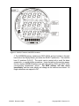
1
MultiComm™ Modbus® RTU Interface Option Manual November 2009 ML0002 Document Revision B © 2009 by Bitronics, LLC -S093 (Formerly DOS9.3) -S103 (Formerly DOS10.3) RS-232C Modbus RTU Protocol RS-485 Modbus RTU Protocol Firmware Version 3.70 and Later Includes Information on CI1 Option (1 Amp Inputs) Includes VI4-480V ac, VI3-277V ac, VI2 – 240V ac and VD4A, VA2, VA4, and VA8 Options TABLE OF CONTENTS TABLE OF CONTENTS ...................................................... i FIRMWARE REVISIONS .................................................... iii CERTIFICATION ................................................................ iv COPYRIGHT ...................................................................... iv INSTALLATION AND MAINTENANCE ............................... iv WARRANTY AND ASSISTANCE ....................................... iv 1.0 DESCRIPTION ............................................................. 1.1 Introduction ........................................................ 1.2 Features ............................................................. 1.3 Specifications ..................................................... 1 1 1 1 2.0 PRINCIPLES OF OPERATION ..................................... 2.1 Modular Construction ......................................... 2.2 Output Connector Board .................................... 2.3 Interface Transceiver ......................................... 2.4 MultiComm Processor Board ............................. 3 3 3 3 3 3.0 MODBUS INTERFACE ................................................. 4 3.1 Description ......................................................... 4 3.2 Modbus Address ................................................ 5 3.3 Transaction Timing ............................................. 5 3.4 Data Format ....................................................... 5 3.4.1 Instantaneous Registers 2½ or 3 Elem ........ 7 3.4.2 Demand Registers 2½ or 3 Elem ............... 10 3.4.3 RTH Summary Registers 2½ or 3 Elem ...... 11 3.4.4 RTH Individual Registers 2½ or 3 Elem ...... 13 3.4.5 Instantaneous Registers 2 Elem ................. 15 3.4.6 Demand Registers 2 Elem .......................... 18 3.4.7 RTH Summary Registers 2 Elem ................ 19 3.4.8 RTH Individual Registers 2 Elem ................ 21 3.5 Writeable Registers ........................................... 23 3.5.1 Setting CT & PT Ratios ............................... 23 3.5.2 Resetting Energy & Demand ....................... 23 3.5.3 TDD Writeable Denominators ..................... 24 3.5.4 Display Screen Configuration Registers ...... 24 3.5.5 Communication Configuration Registers ..... 25 3.5.6 Tag Register ................................................ 26 3.6 Converting Data to Engineering Units ............... 27 3.7 Health Check ..................................................... 30 3.8 Diagnostic LED ................................................. 31 3.9 Heartbeat State Counter ................................... 31 3.10 Meter ID Register ............................................ 32 ML0002 November 2009 i Copyright 2009 Bitronics, LLC. TABLE OF CONTENTS Cont’d. 4.0 MODBUS PROTOCOL ................................................ 33 4.1 Introduction ....................................................... 33 4.2 MODBUS RTU Message Framing .................... 33 4.3 MODBUS RTU Message Content ..................... 33 4.4 MODBUS Function and Exception Codes ......... 34 4.5 Supported MODBUS Commands ...................... 35 5.0 INSTALLATION ........................................................... 38 5.1 Setting Modbus Address ................................... 38 5.2 Modbus RS-232C Link (-S093) ......................... 42 5.3 Modbus RS-485 Network (-S103) ..................... 42 ML0002 November 2009 ii Copyright 2009 Bitronics, LLC. FIRMWARE REVISIONS Modbus Communication Firmware ML0002 Description 1.00 Original MultiComm Modbus Communication Firmware. Used with Version 3.00 MultiComm Meter Firmware 1.10 Added VAs, PF, and Network Writeable CT/PT Ratios. Used with Version 3.30 MultiComm Meter Firmware. 1.20 Added support for optional Demand functions. Used with Version 3.40 MultiComm Meter Firmware. 2.00 Added support for optional RTH (harmonic) functions. Added Tag Register. Added network screen setup. 2.10 Added MultiComm RT (instantaneous models) Fixed Watt/VAR/VA over-range (Version 2.0 returns 7FFFh for <-3000 or >3000) November 2009 iii Copyright 2009 Bitronics, LLC. CERTIFICATION Bitronics LLC certifies that the calibration of its products are based on measurements using equipment whose calibration is traceable to the United States National Institute of Standards Technology (NIST). COPYRIGHT This Option Manual is copyrighted and all rights are reserved. The distribution and sale of this manual are intended for the use of the original purchaser or his agents. This document may not, in whole or part, be copied, photocopied, reproduced, translated or reduced to any electronic medium or machine-readable form without prior consent of Bitronics LLC, except for use by the original purchaser. INSTALLATION AND MAINTENANCE Bitronics' products are designed for ease of installation and maintenance. As with any product of this nature, however, such installation and maintenance can present electrical hazards and should only be performed by properly trained and qualified personnel. If the equipment is used in a manner not specified by Bitronics, the protection provided by the equipment may be impaired. WARRANTY AND ASSISTANCE Products manufactured by Bitronics LLC are warranted against defects in materials and workmanship for a period of thirty-six (36) months from the date of their original shipment from the factory. Products repaired at the factory are likewise warranted for eighteen (18) months from the date the repaired product is shipped, or for the remainder of the product’s original Warranty, whichever is greater. Obligation under this warranty is limited to repairing or replacing, at Bitronics' factory, any part or parts which Bitronics' examination shows to be defective. Warranties only apply to products subject to normal use and service. There are no warranties, obligations, liabilities for consequential damages, or other liabilities on the part of Bitronics except this Warranty covering the repair of defective materials. The warranties of merchantability and fitness for a particular purpose are expressly excluded. For assistance, contact Bitronics LLC at: Telephone: Fax: Email: Website: 610.997.5100 610.997.5450 [email protected] www.novatechweb.com/bitronics Shipping: 261 Brodhead Road Bethlehem, PA 18017-8698 USA ML0002 November 2009 iv Copyright 2009 Bitronics, LLC. 1.0 DESCRIPTION 1.1 Introduction The -S093 and -S103 Modbus 1 RTU SLAVE protocol option for the MultiComm family of instruments is designed to allow operation of these instruments on MODBUS networks. The MODBUS protocol is a widely supported open interconnect originally designed by Modicon. The -S093 option provides point-to-point communication using RS-232C as the physical link. The -S103 option provides multi-drop access to networks using RS-485 as the physical link. 1.2 Features * Rugged Bitronics design * Dedicated communications processor: fast response for maximum instrument polling rates * User selectable instrument address with pushbutton front panel display * Data link activity indicator * Simple command to read any number of instrument quantities * Simple energy and demand reset commands * Supports remote setting of CT and PT scaling factors * "Anti-jabber" hardware on RS-485 transmitter isolates instrument during fault 1.3 Specifications Resolution: Amperes: Volts: Frequency: Watts/VARs/VAs: Per Phase: Total: Power Factor: K Factor: TDD, THD: * 0.1% of 5* A nominal 0.07% of 120V nominal 0.01 Hz 0.1% of 500* secondary Watts nominal 0.1% of 1500* secondary Watts nominal (2 ½ or 3 ELEMENT) 0.1% of 1000* secondary Watts nominal (2 ELEMENT) 0.001 0.01 0.1% - When CI1 Option (1Amp Input) is installed, divide this value by 5 1 ML0002 - MODICON® and MODBUS® are registered trademarks of Schneider Automation November 2009 1 Copyright 2009 Bitronics, LLC. 1.3 Specifications, (Cont’d) Accuracy: Same as base meter (0.25% Class per ANSI Std 460-1988) Modbus Connector: 4-pin Terminal Block for shielded twisted pair Communication: RTU Mode, 9600 Baud, 8 Data, 1 Stop, Even Parity, Half Duplex Interface: 2 wire RS-485 Option -S103, or 3 wire RS-232C Option -S093 Distance: 4,000 ft (1,200m) RS-485, 50 ft RS-232C Functions: Read Holding Registers (FUNC 3) Preset Single Register (FUNC 6) and Preset Multiple Register (FUNC 16) for Writeable Registers Only Diagnostics (FUNC 8 - SUBFUNC 0,0) Diagnostics (Loopback) Response Time: Modbus response begins < 50 msec after valid command received Addressability: Modbus addresses 1..247 (broadcast address 00 not supported) Anti-Jabber: RS-485 line becomes passive within 0.2 seconds of instrument fault EEPROM Memory Endurance: Writeable Registers: 1,000,000 minimum changes per register (Register Writes) ML0002 November 2009 2 Copyright 2009 Bitronics, LLC. 2.0 PRINCIPLES OF OPERATION 2.1 Modular Construction The Bitronics MultiComm instrument option is composed of three major modules. The Modbus network connects to the output connector board which in turn is driven by the interface transceiver which is controlled by the Modbus interface processor. 2.2 Output Connector Board The Modbus network connection is made via the 4 pin terminal block connector on the back of the instrument. An EARTH GROUND input is provided and is connected to the SHIELD terminal through 200 ohms. Both the SHIELD GROUND and the EARTH GROUND input are connected to the MultiComm Processor Board via a 100 ohm resistor. For proper operation of the RS-485 and RS-232C interfaces, the SHIELD GROUND connection must be utilized. If ground potentials under 14 volts can be guaranteed, the EARTH GROUND connection MAY be used but is not required. Refer to Figures 7-9 for the input circuit and connection diagrams. 2.3 Interface Transceiver The communications channel transceiver is located on the analog processing board. This transceiver provides the drive to transmit and receive messages on the Modbus cable. This circuit is an RS-232C transceiver IC for the -S093 option. The -S103 option uses a two-wire RS-485 transceiver IC for this function. The transceiver is connected to the Output Connector Board via the Power Supply Board and a three wire cable to the rear terminal block. 2.4 MultiComm Processor Board The MultiComm Processor Board contains an Intel 80C51FA microcontroller and its associated circuitry. This processor handles all the message reception, error detecting, message transaction and other network overhead required by the Modbus network, as well as communicating with the HOST processor. The HOST processor handles all other functions of the instrument. Approximately every 150 msec (600msec for non “B” models), the MultiComm processor receives a copy of all the data calculated by the HOST processor. The HOST and MultiComm processors communicate via transaction messages that are sent through the DUAL-PORT RAM. ML0002 November 2009 3 Copyright 2009 Bitronics, LLC. Another function of the MultiComm processor is to handle all the Modbus messages. When the MultiComm processor receives a Modbus message, it checks if the Modbus ADDRESS of the message is the address of this instrument. The instrument address is set via two 16-position rotary switches SW3 and SW4, which are also located on this board (See section 5.1 for instructions on setting the instrument address). If the Modbus ADDRESS matches this instrument, the MultiComm processor generates a response. If the message is a READ HOLDING REGISTER, the MultiComm processor generates the response from its copy of the meter data. If the message is a PRESET SINGLE REGISTER or PRESET MULTIPLE REGISTERS (energy/demand resets or CT/PT ratio setups), the MultiComm processor generates a MODBUS response and sends a transaction to the HOST processor. Note that both read and write requests are immediately satisfied using information located on the MultiComm board. The MultiComm processing board also controls the state of the RS-485 transmitter in instruments equipped with the -S103 option. Since RS-485 uses a party-line arrangement, the failure of any instrument to return the transmitter to the passive state after transmission can cause the entire link to malfunction. The MultiComm processing board incorporates hardware which will remove the instrument from the party line if certain timing constraints are not met by the microcontroller. This "anti-jabber" system ensures that a malfunctioning instrument will not cause the communication bus to "lock-up". Status of the Modbus network at this node is indicated by the Diagnostic LED which is located in the upper left hand corner of the MultiComm processor board. This Diagnostic LED is visible through the faceplate, and can been seen in the upper left hand corner of the upper display. Section 3.7 describes the operation of the Diagnostic LED. The CT/PT switch and the select pushbutton are also mounted on the MultiComm Processor Board, however both these switches are read by the HOST processor. A second pushbutton switch is mounted on the faceplate, and connected to the MultiComm Processor board via a pair of wires and a connector. This switch is connected in parallel with the select switch mounted on the MultiComm Processor board, and is used to stop and start the scrolling of the front display (refer to the base MultiComm instrument manual for details). ML0002 November 2009 4 Copyright 2009 Bitronics, LLC. 3.0 MODBUS INTERFACE 3.1 Description The Modbus network is a "MASTER" to "SLAVE" network, that is to say one node asks a question and a second node answers. A NODE is a Modbus device (PLC, Computer, MultiComm instrument, etc.) which is connected to the network. Each SLAVE NODE has an ADDRESS in the range of 1 to 247, and it is this address that allows a MASTER to selectively request data from any other device. Address 0 is a BROADCAST ADDRESS that can be used with certain MODBUS functions to allow the MASTER to address all SLAVE NODES at one time. MultiComm Instruments do not respond to BROADCAST Messages. The Modbus implementation in the MultiComm instrument conforms to all the standard Modbus specifications and capabilities, such as maximum nodes, distance, signal sensitivity, etc. The MultiComm instrument is classified as a SLAVE DEVICE in the Modbus structure. The data items that are available from the instrument can be obtained via the Modbus Network by issuing a READ HOLDING REGISTERS command from the requesting node. 3.2 Modbus Address Each MODBUS instrument responds to a single MODBUS ADDRESS. The address is in the range of 1-247, and each instrument must have a unique address. See section 5.1 for instructions on setting the address. 3.3 Transaction Timing The instrument completes a set of calculations approximately every 100 to 150msec for “B” Models (600msec for “A” Models). At the completion of the calculation the HOST processor services any pending transactions (RESETs and CT/PT ratio setups) and updates the DATA in the MultiComm Processor. Since the MultiComm Processor maintains a copy of the data, all Modbus READs are answered within 50 milliseconds. WRITE requests (reset energy, CT/PT Ratio) are confirmed by the MultiComm processor within 50 milliseconds, but the actual RESET or CT/PT Ratio write will not occur for up to 600 milliseconds, since the MultiComm processor must issue a transaction to the HOST. An additional 10 seconds are required to write to the EEPROM. 3.4 Data Format The instrument contains a set of holding registers (4XXXX) into which the instrument places values that correspond to the measurements the instrument is making. These holding registers can be read by any other device on the network using a READ HOLDING REGISTER (Function Code 3). When using HOLDING REGISTER DATA, the Health Check Register should always be read and checked before interpreting data, since some failure modes will cause erroneous data to be presented (See Section 3.7). The majority of the data is represented in OFFSET BINARY format, for conversion of the register data into ENGINEERING UNITS, please refer to Section 3.6. For specifics concerning the correct ML0002 November 2009 5 Copyright 2009 Bitronics, LLC. command and its implementation, users are directed to the User's manual for the specific device that will request the data. Listed on the following pages are the register assignments for MultiComm Instruments. The available registers depend upon the particular model of MultiComm instrument. The registers have been broken down into four blocks, which are shown in Figure 1. These various blocks are listed on the following pages. Table 1 indicates which blocks pertain to which models. The registers are also divided into two sections by Element Type, 2½ or 3 Element models are in the first section, and 2 Element models are in the second section. Note that unless otherwise specified, all registers are READ-ONLY. ML0002 November 2009 6 Copyright 2009 Bitronics, LLC. Instantaneous Demand RTH Summary RTH Individuals Element Type MTWIE(C)1A,3A,1B,3B X 3 / 2½ MTWIE(C)2A,2B X 2 MTWDE(C)1A,3A X X 3 / 2½ MTWDE(C)2A X X 2 MTWDE(C)1B,3B X X X X 3 / 2½ MTWDE(C)2B X X X X 2 ML0002 November 2009 7 Copyright 2009 Bitronics, LLC. 3.4.1 INSTANTANEOUS Data Registers for 2 ½ or 3 Element Models Quantity Holding Register Representation Health Check 40001 Amperes Phase A Amperes Phase B Amperes Phase C 40002 40003 40004 | | 2047 = 0Amps; 4095 = 10.0*Amps | Volts Phase A-N Volts Phase B-N Volts Phase C-N 40005 40006 40007 | | 2047 = 0Volts; 4095 = 150.0Volts | Watts Total 3 Phase 40008 VARs Total 3 Phase 40009 0 = -3000*Watts; 2047 = 0Watts; 4095 = +3000*Watts 0 = -3000*VARs; 2047 = 0VARs; 4095 = +3000*VARs Watts Phase A Watts Phase B Watts Phase C 40010 40011 40012 | 0 = -1000*Watts; 2047 = 0Watts | 4095 = +1000*Watts | VARs Phase A VARs Phase B VARs Phase C 40013 40014 40015 | 0 = -1000*VARs; 2047 = 0VARs | 4095 = +1000*VARs | CT Ratio PT Ratio 40016 40017 | Normalized ratio (Does not include | decimal point) | 500< Ratio <9999 (CT:5) or | (CT:1 with CT1 option) | 1000 < Ratio < 9999 (PT) Neutral Current 40018 2047 = 0Amps; 4095 = 15.0*Amps + kWatthour (High) + kWatthour (Low) 40019 40020 0=0kWh; 9999=99,990,000kWh 0=0kWh; 9999=9,999kWh - kWatthour (High) - kWatthour (Low) 40021 40022 0=0kWh; 9999=-99,990,000kWh 0=0kWh; 9999=-9,999kWh + kVARhour (High) + kVARhour (Low) 40023 40024 0=0kVARh; 9999=99,990,000kVARh 0=0kVARh; 9999=9,999kVARh - kVARhour (High) - kVARhour (Low) 40025 40026 0=0kVARh; 9999=-99,990,000kVARh 0=0kVARh; 9999=-9,999kVARh * Refer to Section 3.7 - When CI1 Option (1Amp Input) is installed, divide this value by 5 ML0002 November 2009 8 Copyright 2009 Bitronics, LLC. 3.4.1 INSTANTANEOUS Data Registers for 2 ½ or 3 Element Models (Cont’d) Quantity Holding Register Representation Frequency 40027 Unused Unused Unused 40028 40029 40030 Heartbeat State Counter 40031 See Section 3.9 Unused 40032 Always 2047 VAs Phase A VAs Phase B VAs Phase C 40033 40034 40035 VAs Total 3 Phase 40036 2047 = 0VAs; 4095 = 3000*VAs PF Phase A PF Phase B PF Phase C 40037 40038 40039 | 1047 = -1; 2047 = 0; 3047 = +1 | 4046 = Amps or Volts too low | (-) lagging; (+) leading PF Total 3 Phase 40040 1047 = -1; 2047 = 0; 3047 = +1 4046 = Amps or Volts too low (-) lagging; (+) leading CT Ratio 40041 Read/Write normalized ratio, copied to 40016 CT Ratio Divisor 40042 Read/Write; = 1,10,100, or 1000 PT Ratio 40043 Read/Write normalized ratio, copied to 40017 PT Ratio Divisor 40044 Read/Write; = 1,10,100, or 1000 Unused 40045-70 Always 2047 * 0 = <45.00Hz; 4500 = 45.00Hz 7500 = 75.00Hz; 9999 =>75.00Hz | | Always 2047 | | | 2047 = 0VA; 4095 = 1000*VA | - When CI1 Option (1Amp Input) is installed, divide this value by 5 ML0002 November 2009 9 Copyright 2009 Bitronics, LLC. 3.4.1 INSTANTANEOUS Data Registers for 2 ½ or 3 Element Mode (Cont’d) Quantity Holding Register Representation 40071 See Table 4 Meter Type Identifier Communications Firmware Rev. 40072 Host Firmware Rev. 40073 Host Micro Firmware Rev. 40074 | | Packed BCD XX.XX | Unused 40075-91 Display Screen Setup Register 1 Display Screen Setup Register 2 Display Screen Setup Register 3 Display Screen Setup Register 4 Display Screen Setup Register 5 40092 40093 40094 40095 40096 | | | Read/Write - See Table 3 | | Configuration Setup Register 1 Configuration Setup Register 2 40097 40098 | Read/Write - Future Expansion | Always returns 0 User Writeable Tag Register 40099 Read/Write - 0 to 32,767 Energy RESET 40100 Write ONLY; Bit 0 - See Table 2 Unused 40101-103 Always 2047 ML0002 November 2009 10 Always 2047 Copyright 2009 Bitronics, LLC. 3.4.2 DEMAND Data Registers for 2 ½ or 3 Element Models Quantity Holding Register Representation Present Demand Amps φA Present Demand Amps φB Present Demand Amps φC 40045 40046 40047 | | 20471 = 0Amps; 4095 = 10.0*Amps | Max Demand Amps φA Max Demand Amps φB Max Demand Amps φC 40048 40049 40050 | | 20471 = 0Amps; 4095 = 10.0*Amps | Present Demand Amps N 40051 20471 = 0Amps; 4095 = 15.0*Amps Max Demand Amps N 40052 20471 = 0Amps; 4095 = 15.0*Amps Present Demand Volts φA Present Demand Volts φB Present Demand Volts φC 40053 40054 40055 | | 20471 = 0Volts; 4095 = 150.0Volts | Max Demand Volts φA Max Demand Volts φB Max Demand Volts φC 40056 40057 40058 | | 20471 = 0Volts; 4095 = 150.0Volts | Min Demand Volts φA Min Demand Volts φB Min Demand Volts φC 40059 40060 40061 | | 20471 = 0Volts; 4095 = 150.0Volts | Present Demand Watts Total Max Demand Watts Total Min Demand Watts Total 40062 40063 40064 | 0 = -3000*Watts; 20471 = 0Watts | 4095 = +3000*Watts | Present Demand VARs Total Max Demand VARs Total Min Demand VARs Total 40065 40066 40067 | 0 = -3000*VARs; 20471 = 0VARs | 4095 = +3000*VARs | Present Demand VAs Total Max Demand VAs Total Min Demand VAs Total 40068 40069 40070 | | 20471 = 0VAs; 4095 = +3000*VAs | Amp Demand RESET Volt Demand RESET Power Demand RESET 40100 40100 40100 Read/Write Bit 1 - See Table 2 Read/Write Bit 2 - See Table 2 Read/Write Bit 3 - See Table 2 * - When CI1 Option (1Amp Input) is installed, divide this value by 5 - MTWIExB models always return the value 2047 1 ML0002 November 2009 11 Copyright 2009 Bitronics, LLC. 3.4.3 RTH SUMMARY Data Registers for 2 ½ or 3 Element Mode Quantity Holding Register Representation Amp Demand RESET Volt Demand RESET Power Demand RESET Harmonic Demand RESET 40100 40100 40100 40100 Read/Write Read/Write Read/Write Read/Write TDD Denominator Amps φA TDD Denominator Amps φB TDD Denominator Amps φC 40101 40102 40103 | Read/Write 20471 = 0Amps; | 4095 = 10.0*Amps. If reg = 2047, then | Fund Amps will be used (THD) | Factory Default = 5* Amps Secondary Fundamental Amps φA Fundamental Amps φB Fundamental Amps φC 40104 40105 40106 | | 2047 = 0Amps; 4095 = 10.0*Amps | Fundamental Amps Neutral 40107 2047 = 0Amps; 4095 = 15.0*Amps Fundamental Volts φA Fundamental Volts φB Fundamental Volts φC 40108 40109 40110 | | 2047 = 0Volts; 4095 = 150.0Volts | TDD2 Amps φA TDD2 Amps φB TDD2 Amps φC 40111 40112 40113 | | 0 = 0.0%; 9999 = 999.9% | Set to 0 on low signal TDD2 Odd Amps φA TDD2 Odd Amps φB TDD2 Odd Amps φC 40114 40115 40116 | | 0 = 0.0%; 9999 = 999.9% | Set to 0 on low signal TDD2 Even Amps φA TDD2 Even Amps φB TDD2 Even Amps φC 40117 40118 40119 | | 0 = 0.0%; 9999 = 999.9% | Set to 0 on low signal THD Volts φA THD Volts φB THD Volts φC 40120 40121 40122 | | 0 = 0.0%; 9999 = 999.9% | Set to 0 on low signal THD Odd Volts φA THD Odd Volts φB THD Odd Volts φC 40123 40124 40125 | | 0 = 0.0%; 9999 = 999.9% | Set to 0 on low signal THD Even Volts φA THD Even Volts φB THD Even Volts φC 40126 40127 40128 | | 0 = 0.0%; 9999 = 999.9% | Set to 0 on low signal Bit 1 - See Table 2 Bit 2 - See Table 2 Bit 3 - See Table 2 Bit 4 - See Table 2 * - When CI1 Option (1Amp Input) is installed, divide this value by 5 - MTWIExB models always return the value 2047 2 - If TDD Denominator is set to 2047 (0Amps) the TDD calculation will use Fundamental Amps as the Denominator, which will result in all Current Distortions being expressed as THD. 1 ML0002 November 2009 12 Copyright 2009 Bitronics, LLC. 3.4.3 RTH SUMMARY Data Registers for 2 ½ or 3 Element Mode (Cont’d) Quantity Holding Register Representation K-Factor Amps φA K-Factor Amps φB K-Factor Amps φC 40129 40130 40131 | | 100 = 1.00; 65535 = 655.35 | Set to 100 on low signal Displacement PF φA Displacement PF φB Displacement PF φC 40132 40133 40134 | 1047 = -1; 2047 = 0; 3047 = +1 | 4046 = Amps or Volts too low | (-) lagging; (+) leading Displacement PF Total 40135 1047 = -1; 2047 = 0; 3047 = +1 4046 = Amps or Volts too low (-) lagging; (+) leading Present Demand Fund. Amps N 40136 2047 = 0Amps; 4095 = 15.0*Amps Max Demand Fund. Amps N 40137 2047 = 0Amps; 4095 = 15.0*Amps Present Demand TDD1 Amps φA Present Demand TDD1 Amps φB Present Demand TDD1 Amps φC 40138 40139 40140 | | 0 = 0.0%; 9999 = 999.9% | Max Demand TDD1 Amps φA Max Demand TDD1 Amps φB Max Demand TDD1 Amps φC 40141 40142 40143 | | 0 = 0.0%; 9999 = 999.9% | Present Demand THD Volts φA Present Demand THD Volts φB Present Demand THD Volts φC 40144 40145 40146 | | 0 = 0.0%; 9999 = 999.9% | Max Demand THD Volts φA Max Demand THD Volts φB Max Demand THD Volts φC 40147 40148 40149 | | 0 = 0.0%; 9999 = 999.9% | * 1 - When CI1 Option (1Amp Input) is installed, divide this value by 5 If TDD Denominator is set to 2047 (0Amps) the TDD calculation will use Fundamental Amps as the Denominator, which will result in all Current Distortions being expressed as THD. ML0002 November 2009 13 Copyright 2009 Bitronics, LLC. 3.4.4 RTH INDIVIDUAL Data Registers for 2 ½ or 3 Element Mode Quantity Holding Register Representation φA Amps Distortion Denominator 40150 | 2047 = 0Amps; 4095 = 10.0*Amps | =40101 if TDD, =40104 if THD φA Amps Demand Distortion1 - I1 φA Amps Demand Distortion1 - I2 : : φA Amps Demand Distortion1 - I30 φA Amps Demand Distortion1 - I31 40151 40152 | | | 0 = 0.0%; 9999 = 999.9% | Set to 0 on low signal | | : : 40180 40181 φA Volts Distortion Denominator 40182 | 2047 = 0Volts; 4095 = 150.0Volts | =40108 φA Volts Harm. Distortion - V1 φA Volts Harm. Distortion - V2 : : φA Volts Harm. Distortion - V30 φA Volts Harm. Distortion - V31 40183 40184 | | | 0 = 0.0%; 9999 = 999.9% | Set to 0 on low signal | | : : 40212 40213 φB Amps Distortion Denominator 40214 | 2047 = 0Amps; 4095 = 10.0*Amps | =40102 if TDD, =40105 if THD φB Amps Demand Distortion1 - I1 φB Amps Demand Distortion1 - I2 : : φB Amps Demand Distortion1 - I30 φB Amps Demand Distortion1 - I31 40215 40216 | | | 0 = 0.0%; 9999 = 999.9% | Set to 0 on low signal | | : : 40244 40245 φB Volts Distortion Denominator 40246 | 2047 = 0Volts; 4095 = 150.0Volts | =40109 φB Volts Harm. Distortion - V1 φB Volts Harm. Distortion - V2 : : φB Volts Harm. Distortion - V30 φB Volts Harm. Distortion - V31 40247 40248 | | | 0 = 0.0%; 9999 = 999.9% | Set to 0 on low signal | | * : : 40276 40277 - When CI1 Option (1Amp Input) is installed, divide this value by 5 1 If TDD Denominator is set to 2047 (0Amps) the TDD calculation will use Fundamental Amps as the Denominator, which will result in all Current Distortions being expressed as THD. ML0002 November 2009 14 Copyright 2009 Bitronics, LLC. 3.4.4 RTH INDIVIDUAL Data Registers for 2 ½ or 3 Element Mode (Cont’d) Quantity Holding Register φC Amps Distortion Denominator 40278 | 2047 = 0Amps; 4095 = 10.0*Amps | =40103 if TDD, =40106 if THD φC Amps Demand Distortion1 - I1 φC Amps Demand Distortion1 - I2 : : φC Amps Demand Distortion1 - I30 φC Amps Demand Distortion1 - I31 40279 40280 | | | 0 = 0.0%; 9999 = 999.9% | Set to 0 on low signal | | : : 40308 40309 Representation φC Volts Distortion Denominator 40310 | 2047 = 0Volts; 4095 = 150.0Volts | =40110 φC Volts Harm. Distortion - V1 φC Volts Harm. Distortion - V2 : : φC Volts Harm. Distortion - V30 φC Volts Harm. Distortion - V31 40311 40312 | | | 0 = 0.0%; 9999 = 999.9% | Set to 0 on low signal | | * : : 40340 40341 - When CI1 Option (1Amp Input) is installed, divide this value by 5 1 If TDD Denominator is set to 2047 (0Amps) the TDD calculation will use Fundamental Amps as the Denominator, which will result in all Current Distortions being expressed as THD. ML0002 November 2009 15 Copyright 2009 Bitronics, LLC. 3.4.5 INSTANTANEOUS Data Registers for 2 Element Mode Quantity Holding Register Health Check 40001 Amperes Phase A Amperes Phase B Amperes Phase C 40002 40003 40004 | | 2047 = 0Amps; 4095 = 10.0*Amps | Volts Phase A-B Volts Phase B-C Volts Phase C-A 40005 40006 40007 | | 2047 = 0Volts; 4095 = 150.0Volts | Watts Total 3 Phase 40008 VARs Total 3 Phase 40009 0 = -2000*Watts; 2047 = 0Watts; 4095 = +2000*Watts 0 = -2000*VARs; 2047 = 0VARs; 4095 = +2000*VARs Unused Unused Unused 40010 40011 40012 | | Always 2047 | Unused Unused Unused 40013 40014 40015 | | Always 2047 | CT Ratio PT Ratio 40016 40017 | Normalized ratio (Does not include | decimal point) | 500< Ratio <9999 (CT:5) or | (CT:1 with CT1 option) | 1000 < Ratio < 9999 (PT) Unused 40018 Always 2047 + kWatthour (High) + kWatthour (Low) 40019 40020 0=0kWh; 9999=99,990,000kWh 0=0kWh; 9999=9,999kWh - kWatthour (High) - kWatthour (Low) 40021 40022 0=0kWh; 9999=-99,990,000kWh 0=0kWh; 9999=-9,999kWh + kVARhour (High) + kVARhour (Low) 40023 40024 0=0kVARh;9999=99,990,000kVARh 0=0kVARh; 9999=9,999kVARh - kVARhour (High) - kVARhour (Low) 40025 40026 0=0kVARh; 9999=-99,990,000kVARh 0=0kVARh; 9999=-9,999kVARh * Representation Refer to Section 3.7 - When CI1 Option (1Amp Input) is installed, divide this value by 5 ML0002 November 2009 16 Copyright 2009 Bitronics, LLC. 3.4.5 INSTANTANEOUS Data Registers for 2 Element Mode (Cont’d) Quantity Holding Register Frequency 40027 Unused Unused Unused 40028 40029 40030 Heartbeat State Counter 40031 Unused Unused Unused Unused 40032 40033 40034 40035 VAs Total 3 Phase 40036 Unused Unused Unused 40037 40038 40039 PF Total 3 Phase 40040 1047 = -1; 2047 = 0; 3047 = +1 4046 = Amps or Volts too low (-) lagging; (+) leading CT Ratio 40041 Read/Write normalized ratio, copied to 40016 CT Ratio Divisor 40042 Read/Write; = 1,10,100, or 1000 PT Ratio 40043 Read/Write normalized ratio, copied to 40017 PT Ratio Divisor 40044 Read/Write; = 1,10,100, or 1000 Unused 40045-70 Always 2047 * Representation 0 = <45.00Hz; 4500 = 45.00Hz 7500 = 75.00Hz; 9999 =>75.00Hz | | Always 2047 | See Section 3.9 | | Always 2047 | | 2047 = 0VAs; 4095 = 2000*VAs | | Always 2047 | - When CI1 Option (1Amp Input) is installed, divide this value by 5 ML0002 November 2009 17 Copyright 2009 Bitronics, LLC. 3.4.5 INSTANTANEOUS Data Registers for 2 Element Mode (Cont’d) Quantity Holding Register Meter Type Identifier 40071 Communications Firmware Rev. Host Firmware Rev. Host Micro Firmware Rev. 40072 40073 40074 Unused 40075-91 Display Screen Setup Register 1 Display Screen Setup Register 2 Display Screen Setup Register 3 Display Screen Setup Register 4 Display Screen Setup Register 5 40092 40093 40094 40095 40096 | | | Read/Write - See Table 3 | | Configuration Setup Register 1 Configuration Setup Register 2 40097 40098 | Read/Write - Future Expansion | Always returns 0 User Writeable Tag Register 40099 Read/Write - 0 to 32,767 Energy RESET 40100 Write ONLY; Bit 0 - See Table 2 Unused 40101-103 ML0002 November 2009 18 Representation See Table 4 | | Packed BCD XX.XX | Always 2047 Always 2047 Copyright 2009 Bitronics, LLC. 3.4.6 DEMAND Data Registers for 2 Element Mode Quantity Holding Register Present Demand Amps φA Present Demand Amps φB Present Demand Amps φC 40045 40046 40047 | | 20471 = 0Amps; 4095 = 10.0*Amps | Max Demand Amps φA Max Demand Amps φB Max Demand Amps φC 40048 40049 40050 | | 20471 = 0Amps; 4095 = 10.0*Amps | Unused 40051 Always 20471 Unused 40052 Always 20471 Present Demand Volts φA-B Present Demand Volts φB-C Present Demand Volts φC-A 40053 40054 40055 | | 20471 = 0Volts; 4095 = 150.0Volts | Max Demand Volts φA-B Max Demand Volts φB-C Max Demand Volts φC-A 40056 40057 40058 | | 20471 = 0Volts; 4095 = 150.0Volts | Min Demand Volts φA-B Min Demand Volts φB-C Min Demand Volts φC-A 40059 40060 40061 | | 20471 = 0Volts; 4095 = 150.0Volts | Present Demand Watts Total Max Demand Watts Total Min Demand Watts Total 40062 40063 40064 | 0 = -2000*Watts; 20471 = 0Watts | 4095 = +2000*Watts | Present Demand VARs Total Max Demand VARs Total Min Demand VARs Total 40065 40066 40067 | 0 = -2000*VARs; 20471 = 0VARs | 4095 = +2000*VARs | Present Demand VAs Total Max Demand VAs Total Min Demand VAs Total 40068 40069 40070 | | 20471 = 0VAs; 4095 = +2000*VAs | Amp Demand RESET Volt Demand RESET Power Demand RESET 40100 40100 40100 Read/Write Bit 1 - See Table 2 Read/Write Bit 2 - See Table 2 Read/Write Bit 3 - See Table 2 * Representation - When CI1 Option (1Amp Input) is installed, divide this value by 5 - MTWIExB models always return the value 2047 1 ML0002 November 2009 19 Copyright 2009 Bitronics, LLC. 3.4.7 RTH SUMMARY Data Registers for 2 Element Mode Quantity Holding Register Representation Amp Demand RESET Volt Demand RESET Power Demand RESET Harmonic Demand RESET 40100 40100 40100 40100 Read/Write Read/Write Read/Write Read/Write TDD Denominator Amps φA TDD Denominator Amps φB TDD Denominator Amps φC 40101 40102 40103 | Read/Write 20471 = 0Amps; | 4095 = 10.0*Amps. If reg = 2047, then | Fund Amps will be used (THD) | Factory Default = 5* Amps Secondary Fundamental Amps φA Fundamental Amps φB Fundamental Amps φC 40104 40105 40106 | | 2047 = 0Amps; 4095 = 10.0*Amps | Unused 40107 Fundamental Volts φA-B Fundamental Volts φB-C Fundamental Volts φC-A 40108 40109 40110 | | 2047 = 0Volts; 4095 = 150.0Volts | TDD2 Amps φA TDD2 Amps φB TDD2 Amps φC 40111 40112 40113 | | 0 = 0.0%; 9999 = 999.9% | Set to 0 on low signal TDD2 Odd Amps φA TDD2 Odd Amps φB TDD2 Odd Amps φC 40114 40115 40116 | | 0 = 0.0%; 9999 = 999.9% | Set to 0 on low signal TDD2 Even Amps φA TDD2 Even Amps φB TDD2 Even Amps φC 40117 40118 40119 | | 0 = 0.0%; 9999 = 999.9% | Set to 0 on low signal THD Volts φA-B THD Volts φB-C THD Volts φC-A 40120 40121 40122 | | 0 = 0.0%; 9999 = 999.9% | Set to 0 on low signal THD Odd Volts φA-B THD Odd Volts φB-C THD Odd Volts φC-A 40123 40124 40125 | | 0 = 0.0%; 9999 = 999.9% | Set to 0 on low signal THD Even Volts φA-B THD Even Volts φB-C THD Even Volts φC-A 40126 40127 40128 | | 0 = 0.0%; 9999 = 999.9% | Set to 0 on low signal Bit 1 - See Table 2 Bit 2 - See Table 2 Bit 3 - See Table 2 Bit 4 - See Table 2 Always 2047 * - When CI1 Option (1Amp Input) is installed, divide this value by 5 - MTWIExB models always return the value 2047 2 If TDD Denominator is set to 2047 (0Amps) the TDD calculation will use Fundamental Amps as the Denominator, which will result in all Current Distortions being expressed as THD. 1 ML0002 November 2009 20 Copyright 2009 Bitronics, LLC. 3.4.7 RTH SUMMARY Data Registers for 2 Element Mode (Cont’d) Quantity Holding Register Representation K-Factor Amps φA K-Factor Amps φB K-Factor Amps φC 40129 40130 40131 | | 100 = 1.00; 65535 = 655.35 | Set to 100 on low signal Unused Unused Unused 40132 40133 40134 | | Always 2047 | Displacement PF Total 40135 Unused Unused 40136 40137 | | Always 2047 Present Demand TDD1 Amps φA Present Demand TDD1 Amps φB Present Demand TDD1 Amps φC 40138 40139 40140 | | 0 = 0.0%; 9999 = 999.9% | Max Demand TDD1 Amps φA Max Demand TDD1 Amps φB Max Demand TDD1 Amps φC 40141 40142 40143 | | 0 = 0.0%; 9999 = 999.9% | Present Demand THD Volts φA-B Present Demand THD Volts φB-C Present Demand THD Volts φC-A 40144 40145 40146 | | 0 = 0.0%; 9999 = 999.9% | Max Demand THD Volts φA-B Max Demand THD Volts φB-C Max Demand THD Volts φC-A 40147 40148 40149 | | 0 = 0.0%; 9999 = 999.9% | 1047 = -1; 2047 = 0; 3047 = +1 4046 = Amps or Volts too low (-) lagging; (+) leading 1 If TDD Denominator is set to 2047 (0Amps) the TDD calculation will use Fundamental Amps as the Denominator, which will result in all Current Distortions being expressed as THD. ML0002 November 2009 21 Copyright 2009 Bitronics, LLC. 3.4.8 RTH INDIVIDUAL Data Registers for 2 Element Mode Quantity Holding Register φA Amps Distortion Denominator 40150 | 2047 = 0Amps; 4095 = 10.0*Amps | =40101 if TDD, =40104 if THD φA Amps Demand Distortion1 - I1 φA Amps Demand Distortion1 - I2 : : φA Amps Demand Distortion1 - I30 φA Amps Demand Distortion1 - I31 40151 40152 | | | 0 = 0.0%; 9999 = 999.9% | Set to 0 on low signal | | : : 40180 40181 Representation φA-B Volts Distortion Denominator 40182 | 2047 = 0Volts; 4095 = 150.0Volts | =40108 φA-B Volts Harm. Distortion - V1 φA-B Volts Harm. Distortion - V2 : : φA-B Volts Harm. Distortion - V30 φA-B Volts Harm. Distortion - V31 40183 40184 | | | 0 = 0.0%; 9999 = 999.9% | Set to 0 on low signal | | : : 40212 40213 φB Amps Distortion Denominator 40214 | 2047 = 0Amps; 4095 = 10.0*Amps | =40102 if TDD, =40105 if THD φB Amps Demand Distortion1 - I1 φB Amps Demand Distortion1 - I2 : : φB Amps Demand Distortion1 - I30 φB Amps Demand Distortion1 - I31 40215 40216 | | | 0 = 0.0%; 9999 = 999.9% | Set to 0 on low signal | | : : 40244 40245 φB-C Volts Distortion Denominator 40246 | 2047 = 0Volts; 4095 = 150.0Volts | =40109 φB-C Volts Harm. Distortion - V1 φB-C Volts Harm. Distortion - V2 : : φB-C Volts Harm. Distortion - V30 φB-C Volts Harm. Distortion - V31 40247 40248 | | | 0 = 0.0%; 9999 = 999.9% | Set to 0 on low signal | | * : : 40276 40277 - When CI1 Option (1Amp Input) is installed, divide this value by 5 1 If TDD Denominator is set to 2047 (0Amps) the TDD calculation will use Fundamental Amps as the Denominator, which will result in all Current Distortions being expressed as THD. ML0002 November 2009 22 Copyright 2009 Bitronics, LLC. 3.4.8 RTH INDIVIDUAL Data Registers for 2 Element Mode (Cont’d) Quantity Holding Register Representation φC Amps Distortion Denominator 40278 | 2047 = 0Amps; 4095 = 10.0*Amps | =40103 if TDD, =40106 if THD φC Amps Demand Distortion1 - I1 φC Amps Demand Distortion1 - I2 : : φC Amps Demand Distortion1 - I30 φC Amps Demand Distortion1 - I31 40279 40280 | | | 0 = 0.0%; 9999 = 999.9% | Set to 0 on low signal | | : : 40308 40309 φC-A Volts Distortion Denominator 40310 | 2047 = 0Volts; 4095 = 150.0Volts | =40110 φC-A Volts Harm. Distortion - V1 φC-A Volts Harm. Distortion - V2 : : φC-A Volts Harm. Distortion - V30 φC-A Volts Harm. Distortion - V31 40311 40312 | | | 0 = 0.0%; 9999 = 999.9% | Set to 0 on low signal | | * : : 40340 40341 - When CI1 Option (1Amp Input) is installed, divide this value by 5 1 If TDD Denominator is set to 2047 (0Amps) the TDD calculation will use Fundamental Amps as the Denominator, which will result in all Current Distortions being expressed as THD. ML0002 November 2009 23 Copyright 2009 Bitronics, LLC. 3.5 Writeable Registers 3.5.1 Setting CT and PT Ratios The MultiComm instrument is capable of internally storing and recalling CT and PT ratios via the network interface, or through the internal toggle/push-button (Refer to Section 4.1 of the MultiComm User Manual). These ratios are used to scale the display values in engineering (primary) units. These ratios are also used to scale the Energy quantities, registers 40019 through 40026 (Refer to Section 3.4 for register assignments) which are also in primary units. When the CT and PT ratios are set, they are written to registers 40041 through 40044, and are stored in non-volatile memory on the CT/PT Board. Each ratio is stored in two registers, one for the normalized format ratio, and the other for the divisor. Allowable constants for CT Value (40041) are 500 to 9999, and 1000 to 9999 for PT Value (40043). The divisors may be 1, 10, 100, or 1000 only. The number stored will be the high side rating of the CT. A 500:5 ratio CT will have a value of 500 stored, while a 100:1 CT will have a value of 100 stored. For example, to calculate a CT ratio from the data stored in the MultiComm, use the following equation: CT Value (40041) CTRATIO = CT Ratio Divisor (40042) ´ CT Secondary PT Value (40043) PTRATIO = PT Ratio Divisor (40044) The CT and PT ratios values may be used with the equations in Section 3.6 to derive primary unit quantities from the MultiComm. For example, the equation for amperes becomes: AMPEREs = Value - 2047 ´ Full Scale Value ´ CT Ratio 2048 The values stored in registers 40041 and 40043 are duplicated in registers 40016 and 40017 respectively. Registers 40016 and 40017 are READ ONLY and cannot be written to. In the event of a CT/PT Ratio Checksum Failure, the value in the CT Ratio and PT Ratio registers default to 65535 (FFFF Hex), and the value in the CT Ratio Divisor and PT Ratio Divisor default to 0001. See Section 3.6 for more details. WARNING - THE RATIO NON-VOLATILE MEMORY STORAGE HAS A 1,000,000 CYCLE ENDURANCE (RATIOS CAN BE CHANGED 1,000,000 TIMES). ONLY WRITE TO RATIO REGISTERS WHEN THE RATIOS NEED TO BE CHANGED. 3.5.2 Resetting Energy and Demands The Energy and Demand registers can be RESET by writing a bit pattern to Holding Register 40100. Any "1" bits in the proper position cause initiation of the corresponding RESET. Multiple RESETs can be accomplished by using either multiple WRITE commands or a single WRITE command with multiple bits set. Table 2 shows the correspondence between the RESET functions and the bits set. The Registers will be reset within 0.6 seconds, however it may take the meter up to 10 seconds to clear the data ML0002 November 2009 24 Copyright 2009 Bitronics, LLC. stored in the EEPROM. The USER must ensure that the power is not interrupted to the meter for this 10 second period after this command is issued. Bit Position Value Description Registers Affected Global 0 1 Reset (ZERO) Energy 40019 .. 40026 19..26 1 2 Reset AMP Demands 40045 .. 40052, 40136, 40137 N/A 2 4 Reset Volt Demands 40053 .. 40061 N/A 3 8 Reset Power Demands 40062 .. 40070 N/A 4 16 Reset Harmonic Demands 40138 .. 40149 N/A Table 2: Reset Register (40100) WRITE data values 3.5.3 TDD Writeable Denominators The MultiComm instrument is capable of internally storing and recalling Current Values that are used as Denominators in determining the Total Demand Distortion (TDD). The denominator values are stored for each phase, and are stored in Registers 40101, 40102, 40103 for Phase A, Phase B, and Phase C respectively. These denominators affect all Current Harmonic Measurements (Refer to Section 3.4 for register assignments). The Denominators are written to registers 40101 through 40103 over the Modbus communication port, and are stored in non-volatile memory on the Analog Board. The value that needs to be stored follows the same offset binary equation that is used with the other measurements. For 5A secondary, the equation for amperes becomes: AMPEREs = Value - 2047 CT Value ´ 10 ´ CT Ratio Divisor ´ 5 2048 where Value is the Binary Value that should be stored in the denominator register, and Amperes is the actual value of primary current that the user intends for the TDD calculations. The factory default value is 3071 which corresponds to 5 Amps Secondary (1 Amp for CI1 option). If the value stored in the denominator register are set to Zero amps (Value = 2047), then the Harmonic Distortion calculations will use the Fundamental Magnitude of the current, which will result in the Distortion Values to be in the form of THD instead of TDD. The values stored in registers 40101, 40102 and 40103 are duplicated in registers 40150, 40214 and 40278 respectively if the value are non-zero (TDD). If registers 40101,2,3 are set to zero (THD) then the registers 40150, 40214 and 40278 will contain the Magnitude of the Fundamental. WARNING - THE DENOMINATOR NON-VOLATILE MEMORY STORAGE HAS A 1,000,000 CYCLE ENDURANCE (DENOMINATORS CAN BE CHANGED 1,000,000 TIMES). ONLY WRITE TO THE DENOMINATOR REGISTERS WHEN THE DENOMINATORS NEED TO BE CHANGED. ML0002 November 2009 25 Copyright 2009 Bitronics, LLC. 3.5.4 Display Configuration Registers In addition to configuring the display using the internal switches, MultiComm “B” instruments allow the user to configure the front panel display via the network port. This is accomplished utilizing five Display Configuration Registers, which are shown in Table 3. These registers are 16 bits wide, and are programmed in a binary fashion. The lower 8 bits of the first register (register 92) contain status information. Bit 7 (D) is set (bit = 1) if the display has not been configured. If this bit is set, the display will be configured to the factory default setting, which is to show all available screens, and front panel resets enabled. Scrolling of the display screens is controlled by Register 92 bit 6 (S). If this bit is set (bit=1), then the display is in the scrolling mode. The lower 6 bits of register 92 are the present screen number if the display has been stopped (scrolling off). If the display is scrolling, then these 6 bits will be zero. The remaining bits of Register 92, bits 8 through 15, are screen enable bits, with each bit corresponding to a specific screen number. Setting the appropriate bit (bit=1) enables the in screen indicated in the table. Descriptions of the actual screen number indicated in Table 3 are presented in the appropriate MultiComm Instrument Manual. Bit 8 (screen 0) is the “Front Panel Reset Enable” screen, which does not get displayed, but when enabled allows the user to reset Demand Values from the front panel push button. Registers 93 through 96 contain the rest of the screen enables as indicated in Table 3. The upper 8 bits of register 96 are not used. The table also lists the decimal value of each bit position, as an aid in determining the decimal value to place in each register. For example, if a user wanted to enable screens 8, 9, 10 and 20, the user would write the value 4103 decimal (1 + 2 + 4 + 4096 = 4103) to register 93. This is equivalent to writing 0001 0000 0000 0111 Binary or 1007 Hexadecimal to register 93. The Display Configuration is stored in non-volatile memory (EEPROM) and it will be correct after a power outage. WARNING - THE DISPLAY CONFIGURATION NON-VOLATILE MEMORY STORAGE HAS A 1,000,000 CYCLE ENDURANCE (DISPLAY CONFIGURATION CAN BE CHANGED 1,000,000 TIMES). ONLY WRITE TO THE DISPLAY CONFIGURATION REGISTERS WHEN THE DISPLAY CONFIGURATION NEEDS TO BE CHANGED. Bit Position 15 14 13 12 11 10 9 8 7 6 5 4 32 76 8 16 38 4 81 92 40 96 20 48 10 24 51 2 25 6 1 2 8 64 32 16 40092 7 6 5 4 3 2 1 0 D S 40093 23 22 21 20 19 18 17 16 1 5 14 13 12 11 10 9 8 32 3 1 30 29 28 27 26 25 24 Decimal Value 3 8 2 4 1 2 0 1 Register 40094 ML0002 39 38 37 November 2009 36 35 34 33 26 Screen Number if Stopped, Else 0 Copyright 2009 Bitronics, LLC. Bit Position 40095 55 54 53 52 51 50 49 48 Unused 40096 4 7 46 45 44 43 42 41 40 6 3 62 61 60 59 58 57 56 Table 3: Display Configuration Registers (40092 - 40096) 3.5.5 Communication Configuration Registers MultiComm “B” instruments provide READ/WRITE Communication Configuration Registers that allow the user to configure various parameters within the instrument. These Communication Configuration Registers are currently undefined for Modbus, and will always return 0, however they are stored in non-volatile memory (EEPROM) to allow for future upgrades. WARNING - THE COMMUNICATION CONFIGURATION NON-VOLATILE MEMORY STORAGE HAS A 1,000,000 CYCLE ENDURANCE (CONFIGURATION CAN BE CHANGED 1,000,000 TIMES). ONLY WRITE TO THE CONFIGURATION REGISTERS WHEN THE CONFIGURATION NEEDS TO BE CHANGED. 3.5.6 Tag Register MultiComm “B” instruments provide a “TAG” register for user identification purposes. This register is READ/WRITE register that allows the user to write a number from 1 to 32,767 in the tag register. The Instrument will write this value in non-volatile memory EEPROM, so that the value will be available after any power outage. Any attempts to write values above 32,767 will return an illegal value error. Units will be set to 0 from the factory. WARNING - THE TAG REGISTER NON-VOLATILE MEMORY STORAGE HAS A 1,000,000 CYCLE ENDURANCE (THE TAG REGISTER CAN BE CHANGED 1,000,000 TIMES). ONLY WRITE TO THE TAG REGISTER WHEN THE TAG NEEDS TO BE CHANGED. ML0002 November 2009 27 Copyright 2009 Bitronics, LLC. 3.6 Converting Data to Engineering Units As was mentioned in Section 3.4, the majority of the data in both the Global and Holding Registers is stored in a 12-BIT OFFSET BINARY format. This format was chosen to allow efficient use of registers, since both positive and negative quantities can be transmitted without the use of a SIGN (polarity) register. In this format, ZERO (0) is represented as 2047 counts, the most negative number is represented by 0 counts and the most positive number is represented by 4095 counts. While it would appear that this format limits the ACCURACY of the values transmitted in the registers, the RESOLUTION of this method is one part in 2048 which is 0.05%, actually 5 times better than the rated accuracy of the instrument, and therefore has no measurable effect on the accuracy of the transmitted value. When displaying these values at another location, it may be desirable to convert the offset binary format into ENGINEERING UNITS. This conversion is readily accomplished using the following simple scaling equations: BASIC EQUATION FOR OFFSET BINARY: Engineering Units = Value - 2047 ´ Full ScaleSECONDARY ´ Ratio 2048 The CT and PT ratios are the NAMEPLATE ratings of the transducer transformers. The PT ratio in these equations is the same as the PT ratio stored in the transducer since convention is to specify the PT ratio as a ratio to 1. For 5Amp CTs, the CT ratio in these equations is not the same as the ratio stored in the meter, but rather the number stored in the meter divided by 5. This is due to the fact that 5Amp CT ratios are normally specified as a ratio to 5. For 1Amp Cts, the CT ratio is the same as that stored in the instrument. Refer to Section 3.5.1 for more information on the CT/PT Ratios. For example a 500:5 CT and a 4:1 PT would have the following ratios: 500 CTRATIO = 500:5 = 5 = 100 4 PTRATIO = 4:1 = 1 = 4 The Value referred to in the equations would be the value stored in the register that you wished to convert to engineering units. For example if you wanted to convert Phase A Amperes into engineering units, Value would be the value in Holding Register 40002. The ENERGY Registers are stored in the BIN8 format, making these values readily usable with the standard Double Precision Integer Math functions available on PLCs. Using this data format, the address specifying the WORD (both registers) is the address of the first of the two registers in the pair (i.e. the one with the lowest register number). This register will have the most significant portion of the number. If the BIN8 data format is specified, no conversion is required. FREQUENCY is stored as a single binary value that is the actual frequency times 100. PHASE is stored as an offset binary value that is the phase difference times 10. THD and TDD are stored as a single binary value that is the actual THD or TDD times 10. K FACTOR is stored as a single binary value that is the actual K Factor times 100. ML0002 November 2009 28 Copyright 2009 Bitronics, LLC. 2 ½ or 3 ELEMENT EQUATIONS: Value - 2047 x 10* x CT RATIO 2048 Value - 2047 x 15* x CT RATIO AMPEREs N (Inst, Fund, Demand, Max ) = 2048 Value - 2047 x 150 x PT RATIO VOLTs L - N (Inst, Fund, Demand, Min , Max ) = 2048 Value - 2047 x 150 x PT RATIO x 3 VOLTs L - L (Inst, Demand, Min , Max ) (SCALED) = 2048 Value - 2047 WATTs (VARs) (VAs )TOTAL (Inst, Demand, Min , Max ) = x 3000* x PT RATIO x CT RATIO 2048 Value - 2047 WATTs (VARs) (VAs )PER PHASE (Inst) = x 1000* x PT RATIO x CT RATIO 2048 kWh (kVARh) = Value HIGH x 10,000 + Value LOW Value FREQUENCY = 100 Value - 2047 ( - Lag , + Lead ) PF (True, Displacement) = 1000 Value - 2047 ( + Line Leading Ref) PHASE DIFFERENCE = 10 Value THD, TDD(Amps,Volts, Inst, Demand, Max ) = 10 Value K FACTOR = 100 * For CT1 Option, divide this value by 5 AMPEREs(Inst, Fund, Demand, Max ) = ML0002 November 2009 29 Copyright 2009 Bitronics, LLC. 2 ELEMENT EQUATIONS: Value - 2047 x 10* x CT RATIO 2048 Value - 2047 x 150 x PT RATIO VOLTs L - L (Inst, Fund, Demand, Min , Max ) = 2048 Value - 2047 WATTs (VARs) (VAs )TOTAL (Inst, Demand, Min , Max ) = x 2000* x PT RATIO x CT RATIO 2048 kWh (kVARh) = Value HIGH x 10,000 + Value LOW Value FREQUENCY = 100 Value - 2047 ( - Lag, + Lead ) PF (True, Displacement) = 1000 Value - 2047 ( + Line Leading Ref) PHASE DIFFERENCE = 10 Value THD, TDD(Amps,Volts, Inst, Demand, Max ) = 10 Value K FACTOR = 100 * For CT1 Option, divide this value by 5 AMPEREs(Inst, Fund, Demand, Max ) = The above equations provide answers in fundamental units (VOLTs, AMPs, WATTs, VARs, VAs and Hz). If the user desires other units such as KILOVOLTS, KILOWATTS or KILOVARS, the answers given by the equations should be divided by 1,000. If the user desires MEGAWATTS or MEGAVARS, the answers given by the equations should be divided by 1,000,000. Energy values are in units of kWh or kVARh. ML0002 November 2009 30 Copyright 2009 Bitronics, LLC. 3.7 Health Check The following information is contained in the Health Check register (bit 15 is the high order bit and the description indicates the meaning when the bit is set). The Health Check Register should always be read and checked before interpreting data, since some failure modes will cause erroneous data to be presented. Please consult Table I in the base instrument MultiComm Users Manual for a full description of the failures. BIT 0 1 2 3 4 5 6 7 8 9 10 11 12 13 14 15 DESCRIPTION Self Test Fault CT/PT Ratio Checksum Failure 2 CT/PT Board Calibration Checksum Failure 3 Analog Board Calibration Checksum Failure 3 Input Over-Range (Clipping) 4 Program Memory (EPROM) Failure 5 A/D Self-Test Error 5 External Memory (XRAM) Failure 5 Host-MultiComm Interface Crash Phase Calibration Checksum Failure 6 Energy Storage Checksum Failure 7 Demand Storage Parity Error 8 Configuration Parity Error Display Code 2 3 4 6 7 8 9 10 N/A 11 12 13 ---1 ---2 ---3 ---4 ---5 ---6 ---7 ---8 N/A ---9 --10 --11 Future Expansion - will read 0 Future Expansion - will read 0 Future Expansion - will read 0 Will Always Read 0 2 - All measurements except energy are accurate, CT & PT ratio may be corrupted, no display on instrument. All Energies calculated after the failure will be in secondary units ( CTR = 5:5 & PTR = 1:1). 3 - Accuracy of measurements reduced to +/-3% or better. 4 - Accuracy of measurements reduced - dependent on amount of signal overrange. 5 - Data may be corrupted and is unreliable. 6 - Accuracy of WATT/VAR/Energy measurements reduced to +/-0.5% or better. 7 - Stored Energy Data may be corrupted and may be unreliable. 8 - Minimum and Maximum Demand Data may be corrupted. Present Demands unaffected. ML0002 November 2009 31 Copyright 2009 Bitronics, LLC. 3.8 Diagnostic LED The Diagnostic LED is an indicator that shows the communications activity on the Modbus port on the instrument. The Diagnostic LED is a red indicator that is located in the upper left corner of the top display. Because the LED is actually on the board below the Display Board, the Diagnostic LED has a limited viewing angle. The Diagnostic LED will flash every time the MultiComm processor transmits a message. If the LED does not flash when a message is sent to it from a MASTER, check the network for the following problems: * Cable open or short circuit * Defective termination * Incorrect MODBUS ADDRESS * Incorrect polarity of cable connections 3.9 Heartbeat State Counter MultiComm “B” instruments provide a Heartbeat State Counter Register that allows the user to determine when the data is updated within the instrument. This counter will increment by the number of internal 10 millisecond states that have elapsed since the last time the data was updated. Users can use a change in this value as an indication of the instant that the data has been updated in the MultiComm processor. On sequential poles, users can also use the difference in this counter to determine the time that has elapsed between poles. A third use of this register as a visual indicator that the data is changing, allows users of certain MMIs to identify disruption in the polling of the instrument. The Heartbeat State Counter is a full 16bit counter that rolls over at 65535 (655.35 seconds 10.9225 minutes). The counter starts at zero on power-up, and is NOT stored in nonvolatile memory. ML0002 November 2009 32 Copyright 2009 Bitronics, LLC. 3.10 Meter ID Register MultiComm “B” instruments provide an “ID” register for model identification purposes. This register is preprogrammed at the factory, refer to table 4. Model ID Model ID MTWIE1B 20 1 MTWDE1B 30 1 MTWIE2B 20 2 MTWDE2B 30 2 MTWIE3B 20 3 MTWDE3B 30 3 MTWIE4B 20 4 MTWDE4B 30 4 MTWIE5B 20 5 MTWDE5B 30 5 MTWIE6B 20 6 MTWDE6B 30 6 MTWIEC1B - VI3 20 7 MTWDEC1B - VI3 30 7 MTWIEC2B - VI2 20 8 MTWDEC2B - VI2 30 8 MTWIEC2B - VI4 20 9 MTWDEC2B - VI4 30 9 MTWIEC4B - VI3 21 0 MTWDEC4B - VI3 31 0 MTWIEC5B - VI2 21 1 MTWDEC5B - VI2 31 1 MTWIEC5B - VI4 21 2 MTWDEC5B - VI4 31 2 Table 4: Instrument ID Numbers ML0002 November 2009 33 Copyright 2009 Bitronics, LLC. 4.0 MODBUS PROTOCOL 4.1 Introduction The MODBUS protocol is an open standard which defines a command-response method of communicating digital information between a master and slave device. The electrical connection between devices is known as a bus. In MODBUS, two types of devices attach to the bus, master and slave devices. A master device issues commands to slaves. A slave device, such as a MultiComm instrument, issues responses to master commands which are addressed to them. Each bus must contain exactly one master and may contain as many slaves as the electrical standards permit. All devices on a bus must operate according to the same electrical standards (i.e. all must be RS-232C or all must be RS-485). RS-232C standards specify that only two devices may be connected to a bus (i.e. only one slave is allowed). RS-485 specifications allow up to 32 devices (31 slaves) on a bus. The MODBUS protocol specifications define two types of transmission modes: ASCII and RTU. This manual describes only the more common RTU mode. For more information, the manual "MODICON MODBUS PROTOCOL REFERENCE GUIDE" (PI-MBUS-300) may be purchased for a nominal fee directly from Modicon Inc. 4.2 MODBUS RTU Message Framing Each message from either a master or slave consists of a continuous stream of characters. A silent interval of 3.5 character times (3.5 * 11 bits / 9600 baud = 3.5 millisecond) or more separates these streams. Bitronics instruments implement this requirement by waiting for a 3.5 character time gap between characters. If the stream is valid and is addressed to this instrument, then the instrument responds as follows: • Enable the output interface drivers (RS-485 option only) • Wait 5 character times • Send the response as a continuous stream • Wait 3.5 character times • Disable the output interface drivers (RS-485 option only) 4.3 MODBUS RTU Message Content The MODBUS RTU message stream consists of an address byte, a function code byte, a number of message bytes, and two check bytes. The address byte, which is in the range 1 .. 247, specifies the identity of the slave device. The function code byte in a master command indicates the operation which the slave is to perform. The function code byte in a slave response is the same value as the master command function code if no error occurs, otherwise it has 128 added to it. The message bytes in a command contain additional information needed to perform the command. Message bytes in a response contain the data requested if no error has occurred or a one byte exception code upon errors. The check bytes are generated using the CRC-16 polynomial generator sequence (x16 + x15 + x2 + 1) with the remainder pre-initialized to all 1's. The most significant byte of the CRC is transmitted first. ML0002 November 2009 34 Copyright 2009 Bitronics, LLC. 4.4 MODBUS Function and Exception Codes Bitronics instruments currently support the function codes shown in Table 5. Note that the values are shown in hexadecimal (base 16). This table also shows the value which a slave would return upon an error. Master Function Code Slave Error Code Name Meaning 0316 8316 Read Holding Registers Read values from meter 0616 8616 Preset Single Register Write ratio or reset energy/demand 1016 9016 Preset Multiple Registers Write ratio or reset energy/demand 0816 8816 Diagnostics (0,0) Return query data (Loopback) Table 5: Supported MODBUS Function Codes Bitronics instruments return exception codes back to the master upon certain conditions. All functions codes greater than 127 decimal (7F16) indicate a slave error response. The message byte indicates the exception code according to Table 6. Code Name Meaning 1 Illegal Function Master command contained an unrecognized function code. 2 Illegal Data Address Starting address is illegal. Note that some registers are read-only and some are read/write (“A” models had some write only registers). Also returned if meter is in CT/PT set mode. 3 Illegal Data Value Either the register count is invalid or an attempt to write an illegal register value was found. Note that this code can be caused by attempting to read beyond the last instrument register. 4 Slave Device Failure Instrument has failed. If problem persists, please consult the Bitronics factory for assistance. 6 Slave Device Busy More than 6 register WRITE commands (ratio setups or energy/demand resets) have been received within 300 milliseconds. Table 6: Exception Codes ML0002 November 2009 35 Copyright 2009 Bitronics LLC 4.5 Supported MODBUS Commands Bitronics instruments support one read, two write and one diagnostic command. All commands require a register address to be specified in the command. The first register, named 40001 is at hexadecimal address 0000. The energy/demand reset register, named 40100 is at hex address 0063. In commands and responses, the most significant byte of a two byte value is transmitted first. All examples which follow use the hexadecimal values and an instrument address of 001. Read Holding Registers (Function Code 03) This function reads any or all quantities from the Bitronics instrument. The command requires a starting register and the number of registers to read. Attempting to read non-existent registers (or write-only registers in “A” models) will cause an exception. The maximum number of registers which can be read is 103 (44 in “A” models) in non-demand instruments and 341 (70 in “A” models) in demand instruments. Modbus read commands are limited to 125 registers maximum per read request, and Master Blocks (MSTR) are limited to 100 registers maximum per read request. The following example shows two registers being read: TOTAL WATTS (register 40008) with +500 watts per element applied and TOTAL VARS (40009) with -100 VARs per element applied. Byte Name Example 1 2 3 4 5 6 7 8 01 03 00 07 00 02 75 CA Slave Address Function code Start address high Start address low Register count high Register count low CRC-16 low CRC-16 high Notes Total Watts at register 40008 (40008-40001=07) Read 2 registers total Figure 2 - Function Code 03 command (Read Holding Registers) Byte 1 2 3 4 5 6 7 8 9 Name Slave Address Function code Byte count Data high (40008) Data low (40008) Data high (40009) Data low (40009) CRC-16 low CRC-16 high Example 01 03 04 0B FF 07 32 4B C2 Notes 2 registers, 2 bytes each Total WATTs = 0BFF hex = 3071 decimal Total VARs = 0732 hex = 1842 decimal Figure 3 - Function Code 03 response (Read Holding Registers) ML0002 November 2009 36 Copyright 2009 Bitronics LLC Preset Single Register (Function Code 06) This function writes to a single register. An attempt to write to a READ-ONLY register results in an exception. The response is an echo of the command. The following example shows the reset Amp, Volt, and Power demands (writing 14 decimal to register 40100) command. Byte Name Example 1 2 3 4 5 6 7 8 01 06 00 63 00 0E F8 10 Slave Address Function code Start address high Start address low Data high Data low CRC-16 low CRC-16 high Notes 0063 hex = 99 decimal to specify register 40100 000E = 14 decimal = 2 (bit 1) + 4 (bit 2) + 8 (bit 3) Amp + Volt + Power Demand reset Figure 4 - Function Code 06 command and response (Preset Single Registers) Preset Multiple Registers (Function Code 16) This function writes one or more contiguous registers. An attempt to write to a READONLY register results in an exception. The following example shows setting the PT ratio to 1000 : 100 (ie: 10 : 1). Byte Name Example 1 2 3 4 5 6 7 8 9 10 11 12 13 01 10 00 2A 00 02 04 03 E8 00 64 F0 53 Slave Address Function code Start address high Start address low Register count high Register count low Byte count Data high Data low Data high Data low CRC-16 low CRC-16 high Notes 10 hex = 16 decimal 002A hex = 42 decimal to specify register 40043 We write 2 registers (40043 and 40044) Two register, 4 bytes Write 1000 to register 40043 : 03E8 = 1000 decimal Write 100 to register 40044 : 0064 = 100 decimal Figure 5 - Function Code 16 command (Preset Multiple Registers) ML0002 November 2009 37 Copyright 2009 Bitronics LLC Loopback Diagnostic Test (Function Code 08, Subfunction 00) This function performs a communication test without affecting the Bitronics instrument. The command requires two user-supplied data bytes. The entire response message should be identical to the command. This command is typically used to verify existence of a device at a MODBUS address. Byte Name Example 1 2 3 4 5 6 7 8 01 08 00 00 55 AA 5F 24 Slave Address Function code Subfunction high Subfunction low Data high Data low CRC-16 low CRC-16 high Notes Only legal subfunction is 00,00 Any two data bytes are allowed Figure 6 - Function Code 08 command (Loopback Diagnostic Test) Byte Name Example 1 2 3 4 5 6 7 8 01 08 00 00 55 These two data bytes AA are echoed from command 5F 24 Slave Address Function code Subfunction high Subfunction low Data high Data low CRC-16 low CRC-16 high Notes Figure 7 - Function Code 08 response (Loopback Diagnostic Test) ML0002 November 2009 38 Copyright 2009 Bitronics LLC 5.0 INSTALLATION 5.1 Setting Modbus Address The MultiComm instrument provides for direct connection to a Modbus Network. As was mentioned in Section 3.2, each device on a given network must have a different PHYSICAL ADDRESS. A pair of address selector switches (SW3 & SW4) are located on the MultiComm Processor Board, and they are accessible through holes in the Display Board. When the meter is powered, the ADDRESS can be easily checked by pressing the front mounted SELECT button down and scrolling through the available screens ( refer to the MultiComm Users Manual for more details on the screens). After all the screens have been viewed, a marker screen (CT/ID/PT shown below) will be displayed for 1.2 seconds. 5000 CT Ratio 12 ID Address 1000 PT Ratio CTIDPT (5000:5 shown)(5000:1 with CI1 option) (12 shown) (1000:1 shown) This screen serves two purposes - to indicate to the user that all enabled screens have been viewed and to provide the CT/ID/PT information. The Modbus Address is on the middle display. This provides the user with a simple method verifying the address without having to remove the faceplate of the instrument. If the address needs to be changed, the following procedure should be followed: 1. With the MultiComm meter under power, remove the four screws holding the front panel to the meter. Carefully move the front panel away from the instrument to expose the front panel select switch, and disconnect the connector from the display board. Remove the faceplate and gasket. 2. Flip the small toggle switch on the left of the meter UP for CT set (DOWN for PT set). The top display will show the present CT setting, the middle display will show the instrument address and the bottom display will show the present PT setting. The Alphanumeric display will indicate which ratio is being set. Be careful not to push the Select button at this time or the CT\PT ratio will be altered. If the CT and/or PT ratio are accidently changed, refer to the MultiComm Users Manual for instructions on setting the CT/PT ratio. ML0002 November 2009 39 Copyright 2009 Bitronics LLC Figure 8 - Switch, Connector and LED Locations 3. The ADDRESS selector switches are SW3 & SW4, and are located on the right hand side of the Display Board, just below the SELECT pushbutton. The switches have 16 positions (0-9,A-F). The switch can be rotated with a small flat blade screwdriver, or a small phillips screwdriver. Using the table on the next two pages, find the desired MODBUS address and dial the switches SW4 and SW3 to the corresponding hexadecimal values. The NEW address will take effect immediately, and the center display will change as the switches are rotated. All illegal addresses are mapped to 247. ML0002 November 2009 40 Copyright 2009 Bitronics LLC ADD R S W 4 S W 3 ADD R S W 4 S W 3 ADD R S W 4 S W 3 ADD R S W 4 S W 3 2471 1 2 3 4 5 6 7 8 9 0 0 0 0 0 0 0 0 0 0 0 1 2 3 4 5 6 7 8 9 32 33 34 35 36 37 38 39 40 41 2 2 2 2 2 2 2 2 2 2 0 1 2 3 4 5 6 7 8 9 64 65 66 67 68 69 70 71 72 73 4 4 4 4 4 4 4 4 4 4 0 1 2 3 4 5 6 7 8 9 96 97 98 99 100 101 102 103 104 105 6 6 6 6 6 6 6 6 6 6 0 1 2 3 4 5 6 7 8 9 10 11 12 13 14 15 16 17 18 19 20 21 22 23 24 25 0 0 0 0 0 0 1 1 1 1 1 1 1 1 1 1 A B C D E F 0 1 2 3 4 5 6 7 8 9 42 43 44 45 46 47 48 49 50 51 52 53 54 55 56 57 2 2 2 2 2 2 3 3 3 3 3 3 3 3 3 3 A B C D E F 0 1 2 3 4 5 6 7 8 9 74 75 76 77 78 79 80 81 82 83 84 85 86 87 88 89 4 4 4 4 4 4 5 5 5 5 5 5 5 5 5 5 A B C D E F 0 1 2 3 4 5 6 7 8 9 106 107 108 109 110 111 112 113 114 115 116 117 118 119 120 121 6 6 6 6 6 6 7 7 7 7 7 7 7 7 7 7 A B C D E F 0 1 2 3 4 5 6 7 8 9 26 27 28 29 30 31 1 1 1 1 1 1 A B C D E F 58 59 60 61 62 63 3 3 3 3 3 3 A B C D E F 90 91 92 93 94 95 5 5 5 5 5 5 A B C D E F 122 123 124 125 126 127 7 7 7 7 7 7 A B C D E F 1 Illegal MODBUS addresses are converted to ADDRESS 247 ML0002 November 2009 41 Copyright 2009 Bitronics LLC ADD R S W 4 S W 3 ADD R S W 4 S W 3 ADD R S W 4 S W 3 ADD R S W 4 S W 3 128 129 130 131 132 133 134 135 136 137 8 8 8 8 8 8 8 8 8 8 0 1 2 3 4 5 6 7 8 9 160 161 162 163 164 165 166 167 168 169 A A A A A A A A A A 0 1 2 3 4 5 6 7 8 9 192 193 194 195 196 197 198 199 200 201 C C C C C C C C C C 0 1 2 3 4 5 6 7 8 9 224 225 226 227 228 229 230 231 232 233 E E E E E E E E E E 0 1 2 3 4 5 6 7 8 9 138 139 140 141 142 143 144 145 146 147 148 149 150 151 152 153 8 8 8 8 8 8 9 9 9 9 9 9 9 9 9 9 A B C D E F 0 1 2 3 4 5 6 7 8 9 170 171 172 173 174 175 176 177 178 179 180 181 182 183 184 185 A A A A A A B B B B B B B B B B A B C D E F 0 1 2 3 4 5 6 7 8 9 202 203 204 205 206 207 208 209 210 211 212 213 214 215 216 217 C C C C C C D D D D D D D D D D A B C D E F 0 1 2 3 4 5 6 7 8 9 234 235 236 237 238 239 240 241 242 243 244 245 246 247 2471 2471 154 155 156 157 158 159 9 9 9 9 9 9 A B C D E F 186 187 188 189 190 191 B B B B B B A B C D E F 218 219 220 221 222 223 D D D D D D A B C D E F 2471 2471 2471 2471 2471 2471 E E E E E E F F F F F F F F F F F F F F A B C D E F 0 1 2 3 4 5 6 7 8 9 A B C D F F E F 1 Illegal MODBUS addresses are converted to ADDRESS 247 ML0002 November 2009 42 Copyright 2009 Bitronics LLC 4. Return the toggle to the center position. The alphanumeric display will show a Select? prompt for 2 seconds. If the Select button is pressed during the time, the alphanumeric display will indicate Okay, and the user will enter the Display Programming Mode (refer to the MultiComm User's Manual). If the select button is not pressed, the Select? prompt will be followed by a digit check (8888 displayed) and the meter will return to normal operation. 5. Replace gasket, carefully plug in the select switch connector to the two pin connector on the right hand side of the display board. Replace the front cover, being careful to dress the yellow cable to the select switch around the bottom display. Replace the four cover screws. Done!! 5.2 Modbus RS-232C Link (-S093) The Modbus RS-232C Link connects to the instrument via the 4 pin terminal block located on the back of the instrument. Since the RS-232C standard does not allow a transmitter to be disabled, only two devices can be connected to a link (the master and the slave). The pin labeled RXD receives data from the master's transmitter. The instrument sends responses via the TXD pin to the master receiver. Refer to Figure 10 for the connection diagram. 5.3 Modbus RS-485 Network (-S103) The Modbus RS-485 Network connects to the instrument via the 4 pin terminal block located on the back of the instrument. All instruments must be connected in parallel for multidrop configuration, and all instruments must have different Modbus addresses. A 120 ohm terminating resistor must be provided by the user at each end of the RS-485 network. All nodes must be configured to TRISTATE (transmitter disable) when the node is not transmitting. All MultiComm instruments with RS-485 outputs automatically TRISTATE when not transmitting. The "anti-jabber" circuit (refer to section 2.4) ensures that instruments TRISTATE even during a malfunction. MultiComm Modbus instruments will delay their response to a request for a minimum of 10 milliseconds. It is VERY important that the Modbus MASTER device TRISTATE within 10 milliseconds of the last byte of the request being transmitted. Signal polarity of the RS-485 is critical for proper network operation. Connections are made A(-) to A(-), B(+) to B(+) and Shield to Shield. Refer to Figure 11 for the connection diagram. ML0002 November 2009 43 Copyright 2009 Bitronics LLC Figure 9 – Output connector board circuit diagram ML0002 November 2009 44 Copyright 2009 Bitronics LLC MultiComm RS-232C Connections MultiComm Instrument IBM AT DE9 (Female) IBM XT DB25 (Female) Modem DB25 (Male) GND SG TXD RXD Shield 5 2 3 1 7 3 2 1 7 2 3 14 ─── 15 ─── 16 ─── 17 ─── ┌─ └─ 4 6 ┌─ └─ 4 5 ┌─ ├─ └─ 1 7 8 ┌─ ├─ └─ 6 8 20 ┌─ └─ 4 5 Figure 10 - RS-232 (-S093) Output Connection Diagram MultiComm RS-485 Connections MultiComm Instrument RS-485 Device RS-485 to RS-232C Converter GND 14 ─── SHLD 15 ─── A(—) 16 ─── B(+) 17 ─── (See note 1) (See Note 1) SHLD SHLD A A B B Notes: 1.To avoid ground currents in the Shield, Ground (GND) should be connected to Earth Ground at only one end of the RS-485 line. 2. Each device on the RS-485 line must be configured for a 2-wire half-duplex interface. Figure 11 - RS-485 (-S103) Output Connection Diagram ML0002 November 2009 45 Copyright 2009 Bitronics LLC Revision A B C Date 01/30/2009 11/17/2009 Changes Update Bitronics Name, Logo Updated logos and cover page By E. Demicco MarCom Bitronics LLC. 261 Brodhead Road, Bethlehem, PA. 18017 (610) 997-5100 Fax (610) 997-5450 www.novatechweb.com/bitronics