1
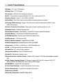
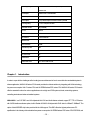
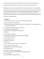
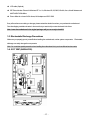
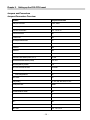
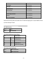
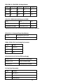
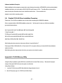
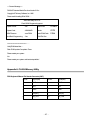
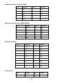
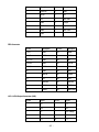
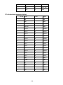
User’s Manual
PPC-1510PT
15.1” TFT Low Power 667Mhz Panel PC
-1-
Ⅰ. Pictures of PPC-157T
VESA-75
Silver (Stainless Steel Color)
VESA-100
I/O ports
-2-
Ⅱ. Panel PC Specifications
◆ Display - 15.1" color TFT flat panel
◆ Display Type - TFT LCD panel
◆ Luminance – 200-250 cd/m2 brightness luminance
◆ CPU - P-III equivalent Low power 667Mhz CPU L1 & L2 cache built on CPU
◆ System Chipset - Twister-T , VIA VT8606 , 82C686B
◆ Front Bezel - Thick 10mm Aluminum-alloy hairline anodizing treatment front bezel
◆ Housing & Wall-mounting - Rugged 1.2mm thick steel metal with white painting VESA–75 and
VESA-100 compliant
◆ Surface Treatment of Front Panel - Super high-end hairline anodizing treatment, color
◆ Standard Colors - Stainless Steel silver color
◆ Front Panel Protection - Meet NEMA 4, 12 and IP65, 56 water resistant EIA standard
◆ System Memory - One slim size CD-ROM, 24x speed built in
◆ CD-ROM (optional) - One slim size CD-ROM, 24x speed built in
◆ HDD (optional) – 10-20 slim size HDD
◆ Disk On Module (optional) - SupportDOMupto512MB
◆ DiskOnChip(optional) - SupportM-System’s DOC upto288MB
◆ Serial ports - 4x COMs ( 3 x RS232 port ,1 xRS232/422/485 port)
◆ USB - 2 x USB ports and IrDA pin header on board
◆ Parallel Port - LPT port for Printer connection.
◆ Keyboard and Mouse - One PS/2 KB/Mouse port
◆ Audio I/O - Microphone, Speaker, Line-in
◆ Network Interface Controller Chipset - Realtek 8139C ,support 10/100 Mbp, auto-negotiation ,auto-switch
LAN
◆ VGA - Display Controller Chipset - S3 Savage 4 ,support AGP 4X LCD/ 2-channel LVDS, TFT,
DSTN LCD/CRT with 32MB share Video memory, 3D/2D support
◆ DVD MPEG-2 - support DVD video playback
◆ Touch Panel (Optional) - Long-life 6-wire resistive Touch screen
◆ Power Requirements - Long-life 6-wire resistive Touch screen
◆ Dimension ( WxHxD) ◆ Operating Temperature - 0 to 55°C (32 to 131°F)
-3-
Ⅲ. Power Supply
Input : 100-240VAC ~ 2A 50/60Hz
DC Output : +5V/7A, +12V/1.5A
-12V/0.3A, +5Vsb/0.75A
Ⅳ. NAGASAKI Panel PC Comparison table
Model no.
SBC
CPU
Power
PPC-64T
NASA-6820
667Mhz on board
AC-DC Adaptor
PPC-70T
MS-2100
300Mhz on board
AC-DC Adaptor
PPC-106T
NASA-6109
667Mhz on board
AC-DC Adaptor
PPC-106T-DC
NASA-6109
667Mhz on board
DC-DC Adaptor
PPC-107PT
NASA-6109
667Mhz on board
AC-DC Adaptor
PPC-107PT-DC
NASA-6109
667Mhz on board
DC-DC Power
PPC-127T
NASA-6109
667Mhz
on board
AC-DC Adaptor
PPC-127T-DC
NASA-6109
667Mhz
on board
DC-DC Adaptor
PPC-128HT
NASA-6104LL
800Mhz
AC-DC Adaptor
PPC-129PT
NASA-6109
667Mhz on board
AC-DC Adaptor
PPC-129PT-DC
NASA-6109
667Mhz on board
DC-DC Adaptor
PPC-156T
NASA-6102
667Mhz on board
AC-DC Power
PPC-157T
NASA-6109
667Mhz on board
AC-DC Adaptor
PPC-157T-DC
NASA-6109
667Mhz on board
DC-DC Adaptor
PPC-158T
NASA-6111
667Mhz on board
AC-DC Power
PPC-159T
NASA-6101
667Mhz on board
AC-DC Power
PPC-1510PT
NASA-6109
667Mhz on board
AC-DC Power
PPC-1510PT-DC
NASA-6109
667Mhz on board
DC-DC Adaptor
-4-
Ⅴ. Touch Panel
1. Application
2. Warranty
3. Features
4. Characteristics
4.1 Usable Temperature Range
4.2 Storage Temperature Range
4.3 Input Method
5. Electrical Specifications
5.1 Linearity
5.2 Insulation Resistance
5.3 Chattering Time
6. Mechanical Specifications
6.1 Operating Force (with pen)
6.2 Surface Hardness
7. Optical Specifications
7.1 Light Transmittance
8. Reliability
8.1 Line drawing operation
8.2 Pen hitting operation
9. Environment Durability Performance
9.1 High Temperature Test
9.2 Low Temperature Test
9.3 Humidity Test
9.4 Thermal Shock Test
9.5 Resistance to Chemical
10. Quality Level
10.1 Inspection condition
10.2 Criterion
10.3 Glass Fragment
10.4 Newton ring
-5-
11. Cautions
1. Application : This specification is applied to 6wire Touch Panel.
2. Warranty : TOUCH PANEL products manufactured to this specification shall be capable of meeting all
characteristics for a minimum period of 12 months the date of shipping from NAGASAKI IPC when stored or used as
specified under normal conditions within the contents of these sheets. If TOUCH PANEL products are not stored or
used as specified herein, it will be void the 12 months warranty.
3. Features
Type :Analog Resistive Type Touch Panel
Input Mode :Polyester Pen or Finger
Structure :Film----- ITO Film Glass----ITO Glass
4. Characteristics
4.1 Operating Temperature Range : From –20℃ to 60℃ (Humidity 90%RH or lower, no dew condition shall be
acceptable)
4.2 Storage Temperature Range : From –30℃ to 70℃
(Humidity 90%RH or lower, no dew condition shall be acceptable)
4.3 Input Method:
(1) with Polyester Pen:
Operation and measurement with a pen must be carried out under the following trip condition:
Material:Polyester
Tip:SR 0.8 millimeter
(2) with Finger:
Operation and measurement with a finger must be carried out under the
Material:Silicon rubber (Hardness: 60º Hs)
Tip: SR 12.5 millimeter
5. Electrical Specifications
5.1 Linearity
Direction:± 1.5% or less (with calibration controller)
5.2 Insulation Resistance: 20 MO or more @ DC 25V
5.3 Chattering Time :10 millisecond or less @ 100KO
6. Mechanical Specifications
Item No. Item Ratings Test Methods & Condition
6-1 Operating Force(with Polyester Pen SR 0.8)
According to applicable product specification Less than 150g Using a load cell with a Polyester Pen conforming to the
specifications set forth in item 4.3 (1) attached to its tip, apply a vertical load within the valid area.
Using themeasurement circuit illustrated in diagram 6-1 below, take the gauge value when the voltage value 4.5V or
greater as the pressure load value.
6-2 Surface Hardness : 2H or Higher JIS-K5400
-6-
7. Optical Specifications
7.1 Light Transmittance (Total Transmittance):More than 78%(Measuring apparatus: Haze meter-made by
BYK-Gardner
Type:Haze–Gard-plus 4726
Illuminant:CIE-A
Standard:ASTM D 1003)
8. Reliability Item No. Item Ratings Test Methods & Condition
8-1 Line drawing operation 1,000,000 times of drawing Requirement in paragraph 5 and 6 Drawing must occur in
following manner at any point within an Action area.
1) Testing equipment:Pen plotter
2) Testing load / force:2.5 N
3) Sliding speed:200 mm / second
4) Tip probe:Polyester Pen as defined in sub-paragraph 4-3(1)
8-2 Pen hitting operation 5,000,000 hits with a pen Requirement in paragraph 5 and 6 Hits must be made in the
following manner at any point within at effective area.
1) Testing equipment:Pen plotter
2) Testing load:2.5 N
3) Press speed:3 hits / second
4) Tip probe:Polyester Pen as defined in sub-paragraph 4-3 (1)
9. Environment Durability Performance Item No. Item Ratings Test Methods & Condition
9-1 High Temperature Test Requirement in paragraph 5 and 6 Put it in a vessel at the condition of 70 ±1℃ and 45
±1% humidity relative for 120 hours. Moreover let it alone for 24 hours or more in a room temperature and measure it.
9-2 Low Temperature Test Requirement in paragraph 5 and 6 Put it in a vessel at the condition of –30 ±1℃ for 120
hours. Moreover, let it alone for 24 hours or more in a room temperature and measure it.
9-3 Humidity Test Requirement in paragraph 5 and 6 Leave in an environment of 60 ±1℃ and 90±1% relative
humility for 120 hours and then perform measurements after leaving at room temperature for 24 hours
9-4 Thermal Shock Test Requirement in paragraph 5 and 6 Put it in a vessel at the condition of 70 ±1℃ for 30
minutes and then –30 ±1℃ for 30minutes and his process is repeated by 10cycles. Moreover let it alone for 24 hours
in a room temperature and measure it.
9-5 Resistance to chemicals (Surface hard coating) No abnormality in external appearance Lightly wipe the surface
with methyl alcohol, artificial perspiration or household cleanser (neutral).
10.Quality Level
10.1 Inspection Condition The inspection shall be performed by using Back light 150-300 cd/m2 ,1000-1400 Lux
(natural light)under the surface of sensor. The panel shall be position sensors from 45cm form eyes and an.
Angle 30 degree (15~45), 15 second viewing time.
-7-
10.2 Criterion The followings are applied to viewing area The item 10.2 (1,2,3,4) should apply to the VA (view area)
unless none VA affect electrical performance
(1) Scratch
Width ≦ 0.1mm and length ≦ 20mm:Accept .
Width > 10 mm or Length > 20mm :Reject
(2) Granular foreign object
Diameter ≦ 0.5mm:Acceptable
0.5mm < Diameter:Unacceptable
(3) Linear foreign object (fiber)
Width ≦ 0.05 and Length ≦5mm:Accept
Width ≧ 0.05 and Length > 5mm:Unacceptable
(4) Blistering (Puffiness, Baggy) Check through any 0.5millimeter gauge whether a Touch Panel surface film does not
contact a measuring face.0.5mm gauge 0.5mm Tablet
10.3 Glass Fragment
(1) Corner Fragment a ≦ 2mm;b ≦ 2mm and(c: break height ≦ t)
:It is acceptable two(t:Glass Thickness)
(2) Side Fragment a ≦ 3mm , b ≦ 2.0mm and c ≦1/2t:acceptable
five and interval of faults is 20mm minimum every side. (t:Glass Thickness)
10.4 Newton ring
Diameter ≦ 35mm,Acceptable
Pass if defect that fails size cannot be seen when held in front of colors program on monitor.
11.Cautions Item No. Subject Note
11.1 Storage 1) Store Touch Panel at the stated temperature and humidity range.
2) Store Touch Panel with original packing.
3) Do not expose Touch Panel directly to the sun
11.2 Unpacking 1) Do not hold FPC / Copper tail to take Touch Panel out of the package.
2) Open the package after checking “UP / DOWN”mark.
3) Do not put the heavy shock and stress on Touch Panel.
11.3 Handling 1) Wear gloves at handling to prevent stains on Touch Panel or injury by the sharp edge of touch glass.
2) Do not hold FPC / Copper while handling Touch Panel.
3) Do not pile Touch Panels and put heavy matter on Touch Panel.
4) Do not add any stress on touch film.
5) Use dry cloth or soft cloth with alcohol, neutral detergent or one with ethanol at cleaning in case of dirt.
6) Do not use organic solvents except alcohol. 11.4 Assembling 1) Avoid excessive force on the Touch Panel.
7) Do not give unnecessary strain to the FPC / Copper tail while assembling.
-8-
Ⅵ. NASA-6109 User’s Manual
Copyright Notice
The content of this manual has been checked for accuracy. The manufacturer assumes no responsibility for any
inaccuracies that may be contained in this manual. The manufacturer reserves the right to make improvements or
modification to the this document and/or the product at any time without prior notice. No part of this document may be
reproduced, transmitted, photocopied or translated into any language, in any form or by any means, electronic,
mechanical, magnetic, optical or chemical, without the prior written permission of the manufacturer. VIA is registered
trademark of VIATechnology Incorporation VT82C686A may only be used to identify products of VIATechnology
Realtek is registered trademark of Realtek Technologies Inc. Multiscan is a trademark of Sony Corp of America IBM,
EGA, VGA, PC/XT, PC/AT, OS/2 and PS/2 are registered trademarks of International Business Machines Corporation
Intel is a registered trademark of Intel Corporation Plug and Play is registered trademarks of Intel Corporation Microsoft,
Windows and MS-DOS are trademarks of Microsoft Corporation Award is a trademark of Award Software Inc. PCI is a
registered trademark of PCI Special Interest Group Other product
names mentioned herein are used for identification purpose only and may be trademarks and/or registered trademarks
of their respective companies.
Installation Notice
The manufacturer recommends using a grounded plug to ensure proper motherboard operation. Care should be used
in proper conjunction with a grounded power receptacle to avoid possible electrical shock. All integrated circuits on this
motherboard are sensitive to static electricity. To avoid damaging components from electrostatic discharge, please do
not remove the board from the anti-static packing before discharging any static electricity to your body, by wearing a
wrist-grounding strap. The manufacturer is not responsible for any damage to the motherboard due to
improper operation.
Specification
This manual covers two different layout models, and the respective board layouts are shown in chapter 1-4. Please
refer to the following description to make sure which model on hand before using.
MODEL
System Chipset
NASA-6109
VIA PM133 , VT8601/VT686B
-9-
CPU Supporting
Embedded VIA EDEN ESP5000 (533MHz) or VIA c3
800MHz CPU
LAN Adapter
Realtek 8139C or Intel 82559ER
Audio Adapter
*Optional
VGA Adapter
On chip 2D/3D Graphic Controller w/ SMA up to 8MB
LCD Supporting
TFT TTL LCD optional LVDS l
ROM-Disk Socket
Yes (2-288MB)
TV-Out
Optional
I/O Port
4S/2P
IDE Interface
U. DMA 33/66/100
DIMM Socket
1
Max. RAM Size
512MB
VGA Memory Size
8MB
Watch Dog Timer
Optional
AT / ATX Power
Yes
USB Feature
Yes
Board SizeFormat
203 x 146mm SBC Format
Chapter 1. Introduction
In order to cope with the challenges of the heating issues and demand of much more diminutive embedded system in
diverse application, NASA-6109 series CPU boards provides the ultimate solution by integrating with VIA’s technology
low power consumption VIA C3 series CPU and VIA EDEN fanless ESP series CPU. NASA-6109 series CPU boards
offer the assorted functions for various applications such as high-end POS systems, kiosks, networking systems,
controlling terminals and other embedded systems.
NASA-6109 is a 5.25”SBC uses VIA chipsets built-in VGA and Audio feature onboard, support TFT TTL LCD feature
with LVDS interface as feature option; built-in Realtek 8139XX LAN chipset with RJ45 Jack for 10BaseT/ 100BaseT. The
option of Intel 82559ER chip is also provided for the LAN support. This SBC offers the highest performance PC
specification in the industry with embedded low power consumption VIA EDEN fanless ESP series CPU ESP5000, and
- 10 -
with the option of the higher performed VIA C3 800MHz CPU. For easier assembly and better integration without
arranging array of cables, NASA-6109 provides onboard connectors with a similar conventional ATX layout.
NASA-6109 provides the option of integrating Watch Dog Timer for ideal unattended terminals. To offer better flexibility, it
also provides the options of riser card for PCI or ISA expansion through a 188-pin slot. This CPU board is fully compatible
with industry standards, adding many technical enhancements and are fully compatible with thousand of software
application such as WIN 95, 98, WIN NT 3.x / 4.x, WIN 2000, WIN ME, WIN CE (.NET), LINUX, UNIX, Novell… etc. The
control logic provides high-speed performance for the most advanced multi-user, multitasking application available today.
“Tomorrow’s PC technology is here today”.
1-1. Features
◆ NASA-6109, embedded VIA C3 TM, Eden TM, Ezra TM Low Power EBGA processors.
◆ 133 / 100 / 66 MHz CPU Front Side Bus (FSB)
◆ DRAM interface synchronous or pseudo synchronous with CPU FSB speed of 133 / 100 / 66 MHz Mixed 1M / 2M /
4M / 8M / 16M / 32MxN DRAMs
◆ 1 or 2 DIMM 168 Pin socket supported up to 512MB or 1.0GB
◆ 3.3V DRAM interface with 5V-tolerant inputs
◆ Support Dual channel UltraDMA-100 / 66 / 33 enhance IDE
◆ AC-97 link.
◆ On-board built-in 2 or 4 USB ports.
◆ Integrated Super-I/O support 4 Serial with power selector and 2 parallel ports.
◆ Optional RS-422/485 via COM2
◆ System Hardware monitoring
◆ Keyboard / mouse interfaces.
◆ RTC / CMOS
◆ PCI-2.2 compliant, 32 bit 3.3V PCI interface with 5V tolerant inputs.
◆ 33 MHz operation on the primary PCI bus
◆ 188pin expansion slot for both PCI and ISA Bus signals.
◆ PC99 Hardware Support
◆ Watch-Dog-Timer support 1-255sec programmable.
◆ On-board support Realtek or Intel 82559/ER 10/100 LAN adapter with RJ-45 port.
◆ AGP v1.0 compliant
◆ Integrated AGP Bus 2D / 3D graphic accelerator.
- 11 -
◆ Windows 95 OSR-2 VXD and integrated Windows 98 / NT5 miniport driver support
◆ BIOS shadow at 16KB increment
◆ Supports 2, 4 and 8 Mbytes of Frame Buffer with share memory.
◆ DirectDrawTM and DirectVideoTM Hardware Support
◆ Advanced Mobile Power Management
◆ CRT Power Management (VESA™ DPMS)
Optional for Flat Panel Interface ( TTL or LVDS )
The board is designed to support industry standard TFT panel via 44pin connector or LVDS transmitters. The interface
supports both 18-bit and 24-bit display modes. Optionally, an 18+18 panel can be supported utilizing external latches.
Optional Features
◆ Supports RS422/RS485 interface with COM2
◆ Support LVDS LCD panel
◆ Supports Audio function (via AV Card Kit)
◆ Supports TV-Out feature (via TV-Out adapter Kit)
◆ Support Watch Dog Timer / POST code (WDT only for NASA-6109)
◆ Support BOOT ROM
Ordering information
NASA-6109
1. NASA-6109VLA: Support 1 LAN
2. NASA-6109LVDS: Support 1 LAN + LVDS
Note: The standard version of NASA-6109 is embedded with VIA EDEN Fanless 533Mhz and 667MHz .
Other option CPUs will be provided upon request.
1-2. Unpacking
The motherboard comes securely packaged in a sturdy cardboard shipping carton. In addition to the User's Manual, the
motherboard package includes the following items:
◆ NASA-6109 5.25”SBC / CPU Board
◆ HDD/FDD Cables
◆ TV-Out adapter / cable (Optional)
◆ Audio Kit (Optional)
- 12 -
◆ LCD cable (Optional)
◆ IDE Driver includes: Drivers for Windows NT 3.x / 4.x, Windows 95, 98, 2000, Win Me, Linux, Novell Netware and
AMI FLASH ROM utilities.
◆ Driver utilities for on-board VGA drivers, LAN adapter and DOC 2000
If any of these items are missing or damage, please contact the dealer from whom you purchase the motherboard.
Save the shipping material and carton in the event that you want to ship or store the board in the future.
Note: Leave the motherboard in its original package until you are ready to install it !
1-3. Electrostatic Discharge Precautions
Make sure you properly ground yourself before handling the motherboard, or other system components. Electrostatic
discharge can easily damage the components.
Note: You must take special precaution when handling the motherboard in dry or air-conditioned environments
1-4. 5.25” SBC (NASA-6109)
- 13 -
Chapter 2. Setting up the 6109 CPU board
Jumpers and Connectors
Jumpers/Connectors Overview:
Function
Jumpers/Connectors
Cooling Fan Connector
JFAN1, JFAN2
Power Supply: Power Good
JP12: Pin 9~11
ATX Power On/Off Switch
JP12: Pin 12~13
Audio Port Connector
CN1
2nd Printer Port
CN4
LAN Adapter Disable/Enable
JP3
COM1 Port
CN6
COM2 Port
CN8
COM3 Port
CN2
COM4 Port
CN3
COM Ports Power Selector (COM1, 2, 3, 4)
JP4, JP9
RS232/RS422/RS485 Selector (COM2)
JP10, JP11
DiskOnChip Memory Address
JP15
LCD: TFT LCD Panel Connector
LCD-CON1
LVDS LCD Output Port
CN5
LVDS Voltage Selector
JP5
Clear CMOS
JP2
Factory Setting
JP1, JP7, JP8, JP13, JP14, JT1, JH1
PS/2 Keyboard Jack
JKBMS
PS/2 Mouse Jack
JKBMS
PS/2 Mouse/KB Pin Header
CN7
IR
J1
FDD Connector
FDD1
IDE 1
IDE1
Header for Case Panel
JP12
IDE 1 LED
JP12: Pin 1, Pin 2
- 14 -
Function
Jumpers/Connectors
External Speaker
JP12: Pin 3, Pin 6
Buzzer On/Off
JP12: Pin 4, Pin 5
Hardware Reset Switch
JP12: Pin 7, Pin 8
External Power Good
JP12: Pin 9, Pin 10
Internal Power Good
JP12: Pin 10, Pin 11
ATX Power Supply On/Off Switch
JP12: Pin 12, Pin 13
Power LED
JP12: Pin 14, Pin 15
WDT Function Enable/Disable
JP12: Pin 19, Pin 20
Please double-check the insertion and orientation of the LCD cable before applying power : mproper installation will result
in permanent damage LCD panel.
JP2: CMOS Data Clear:
Pin 1-2 *
Normal
Pin 2-3
Clear CMOS Data
JP15: DiskOnChip Memory Address Selector
JP15
Memory Address
1-2
7-8
0C800H-0C9FFH
1-2
9-10
0CC00H-0CDFFH
3-4
7-8
0DCCCH-0D1FFH
3-4
9-10
0D400H-0D5FFH
5-6
7-8
0D800H-0D9FFH(Default)
JP3: On-board LAN Disable/Enable
Pin 1-2
Enable On-Board LAN
Pin 2-3
Disable On-Board LAN
- 15 -
JP9 (COM1, 2) / JP4 (COM3, 4) Voltage Selector:
Voltage
COM1(JP9) COM2(JP9) COM3(JP4) COM4(JP4)
+12V(dc) 1-2
7-8
1-2
7-8
R.I.
3-4
9-10
3-4
9-10
+5V(dc)
5-6
11-12
5-6
11-12
JP10, JP11: RS232 / 422 / 485 Selector for COM2
TYPE
JP10
JP11
RS-232
1-2, 4-5, 7-8, 10-11
1-2
RS-422/485 Full Duplex
2-3, 5-6, 8-9, 11-12
3-4, 7-8
* Make sure the port mode is set up correctly before installing any peripherals.
JP12’s Pin 9~11: On-board Power Good Selector
Pin 9-10
Using External Power Good
Pin 10-11
Using On Board Power Good
JFAN1, JFAN2: CPU / 2nd Cooling Fan Connector
Pin No.
Function
Pin 1
Sensor Pin.
Pin 2
+12V
Pin 3
GND
JP12’s Pin12;13;16;17;18: For ATX Power Supply
Close Pin 16-17
Using PS/2 AT Power Supply
Close Pin 17-18
Using ATX Power Supply
Pin 12; Pin 13
On/Off Switch for ATX Power
12: Case Panel Connection:
Pin No.
Description
1,2
HDD_LED -/+
3,6
External Speaker
4,5
Onboard Buzzer
- 16 -
7-8
Hardware RESET
9-10
Reserved
10-11
Reserved
12-13
ATX Power On/Off
14-15
Power LED (14:LED+, 15:LED-)
16-17
Close for PS/2 Power
17-18
Close for ATX Power
19-20
Close: Enable WDT function
J1: IR Pin Header.
Pin No.
Function
1
+5V(DC)
2
N.C.
3
IRRX
4
GND.
5
IRTX
CN1: Audio Output Port connector via AV Card Kit (Optional)
Please close pin13-14 to disable onboard Audio features if the AV Card Kit is not inserted onto the CN1 connector. If AV
card kit is inserted, please make sure the BIOS is enabled with the audio function, since LPT2 and audio function can not
be used in the same tim
CN1: Audio Port.
Pin No.
Function
Pin No.
Function
1
BITCLK
2
GND
3
SDIN
4
N.C.
5
SDIN2
6
N.C.
7
SDOUT
8
N.C.
9
SYNC
10
GND
11
-ACRST
12
GND
13
SPEAK
14
Strapping Low
15
+5V(DC)
16
+12V(DC)
- 17 -
17
JBCY
18
JAB2
19
JBCX
20
JAB1
21
JACY
22
JBB2
23
JACX
24
JBB1
25
MSO
26
MSI
CN7: Pin Header for PS2 KB / MS
Pin No.
Signal (KB)
Pin No.
Signal(MS)
1
KB Data
2
MS Data
3
KEY
4
KEY
5
GND
6
GND
7
+5V(DC)
8
+5V(DC)
9
KB_CLK
10
MS_CLK
Printer (LPT1/LPT2) Port
Pin No.
Description
Pin No.
Description
1
STB#
10
ACK#
2
PD0
11
BUSY
3
PD1
12
PE
4
PD2
13
SLCT
5
PD3
14
AFD#
6
PD4
15
ERR#
7
PD5
16
INIT#
8
PD6
17
SLIN#
9
PD7
18-25
GND
JP5: Voltage Selector for LDVS Receiver
Pin No.
Signal
1-2
Receiver = +5V(DC) Type
2-3
Receiver = +3.3V(DC) Type
4-5
Open for OEM. Type
- 18 -
Close for Normal Type
* Caution: Improper setting will damage LCD panel.
CN5: LCD - LVDS Output.
Pin No.
Signal
Pin No.
Signal
1
Y0-
2
Y2-
3
Y0+
4
Y2+
5
Y1-
6
Rcv. Voltage
7
GND
8
Y3-
9
Y1+
10
Y3
11
CK-
12
VDD_PNL
13
CK+
14
DISP_OFF
15
VBL
16
GND
LCD_CON1: TFT LCD Panel Port
Pin No.
Signal
Pin No.
Signal
1
VBL
2
VBL
3
GND
4
GND
5
VDDLCD
6
VDDLCD
7
ENPVEE
8
GND
9
FPD 23
10
FPD 22
11
FPD 17
12
FPD 16
13
FPD 11
14
FPD 10
15
FPD 9
16
FPD 8
17
FPD 21
18
FPD 20
19
FPD 15
20
FPD 14
21
FPD 7
22
FPD 6
23
FPD 5
24
FPD 4
25
FPD 19
26
FPD 18
27
FPD 13
28
FPD 12
29
FPD 3
30
FPD 2
- 19 -
31
FPD 1
32
FPD 0
33
GND
34
GND
35
P_CLK
36
FLM
37
DE
38
LP
39
GND
40
PBKL
41
PNKL
42
KEY
43
VCC
44
VCC
* Please make sure the Pin 1 location before inserting the LCD connector.
Factory Setting:
JP1: All Pin Open
JP7: Close Pin 1-3, Pin 4-6
JP8: Close Pin 1-2
JP13: Factory Using only
JP14: Close Pin 2-3; Pin 5-6; Pin 8-9; Pin 11-12
JT1: Close Pin 2-3; Pin 4-5; Pin 8-9
JH1: Close Pin 1-2; Pin 5-6; Pin 7-8
2-4.
Installing Memory
The NASA-6109 CPU board offers one 168pin DIMM sockets
supporting up to 512MB of memory. The DIMM memory can be 100MHz (PC-100) or 133 MHz (PC-133).
2-5.
Shared VGA Memory
The NASA-6109 is using built-in AGP VGA controller with share memory architecture (SMA) - AGP mode with 2MB to
8MB of system memory. The amount of video memory on motherboard determines the number of colors and the
video graphic resolution.
2-6.
Installing Riser Card
Installing Riser Card (Max. 3 PCI Slot on Riser Card)
PCI Slot
INT
ADSEL
PCI 1
A,B,C,D
AD24(Onboard LAN)
PCI 2
B,C,D,A
AD23
PCI 3
C,D,A,B
AD22
PCI 4
D,A,B,C
AD21
- 20 -
There are two different riser cards that can be fitted to NASA-6109 CPU board. The first one is a 98pin ISA only Bus
riser card (traditional ISA Bus riser card), the second one is a 188pins PCI/ISA riser card.
Please note: PCI/ISA riser cards jumper settings have to be matched with the motherboard INT/AD-select
jumper.
The default INT/AD-select for NASA-6109/3601M All-In-One motherboard is listed in the above table. However, it could
be revised by changing JP14 setting for different INT/AD-select. The following table shows the variable configurations:
INT/AD Configurations:
Expansion for PCI Slot
* Close 1-2
Close 2-3
Expansion PCI 1
INT =A,B,C,D
INT = B,C,D,A
Expansion PCI 2
INT = B,C,D,A
INT = C,D,A,B
Expansion PCI 3
INT = C,D,A,B
INT = D,A,B,C
Expansion PCI 4
INT = D,A,B,C
INT = A,B,C,D
Note: Even change the setting for different configuration the AD-select should be match to each INT. Please using the
default setting as above if you are not familiar with the configuration of raiser card and add-on card.
Caution: Do not insert PCI Bus Add-On cards directly into the on-board expansion slot!
2-6.
Assigning IRQs for Expansion Cards
Some expansion cards require an IRQ (Interrupt request vector) to operate. Generally, each IRQ must be exclusively
assigned to specific use. In a standard design, there are 16 IRQ available with 11 of them already in used by other part
of the system.
Both ISA and PCI expansion cards may need to use IRQ. Cards installed in the ISA Expansion Bus have the first
priority to use the available system IRQs. Any remaining IRQ then, may be assigned to this PCI Bus. Microsoft's
Diagnostic (MSD.EXE) utility included in the Windows directory can be used to see their map. Make sure that there are
no two devices using the same IRQ in the system. Otherwise this will cause the system to hang up or give unexpected
results. To simplify the process, this motherboard complies with the Plug and Play (PnP) specifications, which was
developed to allow automatic system configuration. Whenever a PnP-compliant card is added to the system, PnP cards
and IRQs are automatically assigned if available. If the system has both Legacy and PnP ISA cards installed. IRQs
are assigned to PnP cards from those not used by Legacy cards. The PCI and PnP configuration in the BIOS setup
utility can be used to indicate
which IRQs have being used by Legacy cards. For older Legacy cards that do not work with the BIOS, you can contact
your vendor for an ISA configuration utility.
- 21 -
An IRQ number is automatically assigned to PCI expansion cards after those used by Legacy and PnP ISA cards. In
the PCI Bus design, the BIOS is automatically assigned an IRQ to a PCI slot that has a card in it which requires an IRQ.
To install a PCI card, you need to set the correct "ADSEL" and "INT" (interrupt) assignment. Please refer to "Chapter
2-5" Installing a Riser Card for detail assignments.
IRQ
Status
Assignment
0
Used
Timer
1
Used
Keyboard
2
Used
Second 8259
3
Used
COM2
4
Used
COM1
5
Used
COM3
6
Used
Floppy Disk
7
Used
LPT1
8
Used
RTC
9
Used
LPT2 or Audio
10
Used
COM4
11
Used
LAN Adapter (on board)
12
Used
PS/2 Mouse
13
Used
Coprocessor
14
Used
Hard Disk (IDE 1)
15
Used
Reserved (IDE 2)
2-8. Assigning DMA Channels for ISA Cards
Since ISA cards, both Legacy and PnP may also need to use a DMA (direct memory access) channel, DMA
assignments for this motherboard are handled the same way as the IRQ assignment process described above. You
can select a DMA channel in the PCI and PnP configuration section of the BIOS setup utility. In the BIOS setup, you
should choose "Yes" for those IRQ's and DMA's you wish to reserve for Legacy cards.
- 22 -
Chapter 3. AMI BIOS SETUP
AMI BIOS Setup Main Menu
Standard CMOS Setup
Advanced CMOS Setup
Advanced Chipset Setup
Power Management Setup
PCI / Plug and Play Setup
Peripheral Setup
Hardware Monitor Setup
Setup HDD Security Password
Auto-Detect Hard Disks
Change User Password
Change Supervisor Password
Change Language Setting
Auto Configuration with Optimal Settings
Save Settings and Exit
Exit Without Saving
Use the CMOS setup program to modify the system parameters to reflect the environment installed in your system and
to customize the system as desired. Press the <DEL> key to enter into the CMOS setup program when you turn on
the power. Settings can be accessed via arrow keys. Press <Enter> to choose an option to configure the system
properly.
In the main menu, press F10 or “SAVE & EXIT SETUP”to save your changes and reboot the system.
Choose “EXIT WITHOUT SAVING”to ignore the changes and exit the setup procedure. Pressing <ESC> at
anywhere during the setup will return to the main menu.“Advanced CMOS Setup”, “Details of the Advanced Chipset
Features”and “PCI / Plug and Play Setup”requires board knowledge on PC/AT system architecture and VIA chipset
specification. They intend to be used by well-trained technicians and experienced users. Incorrect setup could cause
system malfunctions.
3-1.
Quick Setup
3-2.
In most cases, you can quickly configure the system by using the following procedure.
The manufacturer highly recommends that you use “Quick Setup”for setting CMOS to avoid any unpredictable results.
Choose “Standard CMOS Setup”from the main menu, to configure the date and time, hard disk type, floppy disk drive
type etc.
- 23 -
Choose “Auto Configuration with Optimal Setting”from the menu for loading the defaults parameters that is set by the
manufacturer for the most stable normal configuration.
Press F10 or “Save Setting and Exit”to save the changes and reboot the system.
3-2. Description of the BIOS Setup Option
Please make clear the means of those optional parameters. Improper settings will cause the system to hang up or
perform poorly. Most items are clearly understood from the screen prompt or “Help”by function key “F1”. The
manufacturer highly recommends that “Default”settings have been used to avoid any unpredictable results.
3-3. Advanced CMOS Setup
Advanced CMOS Setup
Quick Boot
Enabled
1st Boot Device
Floppy
2nd Boot Device
IDE-0
3rd Boot Device
CDROM
4th Boot Device
Disabled
Try Other Boot Devices
Yes
S.M.A.R.T. for Hard Disks
Disabled
BootUp Num-Lock
On
Floppy Drive Swap
Disabled
Floppy Drive Seek
Disabled
PS/2 Mouse Support
Enabled
Typematic Rate
Fast
System Keyboard
Present
Primary Display
VGA/EGA
Password Check
Setup
Boot To OS/2
No
System BIOS Cacheable
Enabled
C000, 32k Shadow
Cached
C800, 16k Shadow
Disabled
CC00, 16k Shadow
Disabled
D000, 16k Shadow
Disabled
- 24 -
D400, 16k Shadow
Disabled
D800, 16k Shadow
Disabled
DC00, 16k Shadow
Disabled
S.M.A.R.T. For Hard Disks
Set this option to “Enabled”to permit AMIBIOS to use the SMART (System Management System Management and
Reporting Technologies) protocol for reporting server system information over a network. The settings are “Enabled”or
“Disabled”.
Password Check
This option enables password checking every time the system boots or when you run AMIBIOS Setup. If Always is
chosen, a user password prompt appears every time the computer is turned on. If Setup is chosen, the password
prompt appears if AMIBIOS is executed. See the Advanced Setup chapter for instructions on changing a password.
Boot To OS/2
Set this option to “Enabled”if running OS/2 operating system and using more than 64 MB of system memory on the
motherboard. The settings are “Enabled”or “Disabled”.
System BIOS Cacheable
When set to “Enabled”, the contents of the F0000h system memory segment can be read from or written to cache
memory. The contents of this memory segment are always copied from the BIOS ROM to system RAM for faster
execution. The settings are “Enabled”or “Disabled”.
3-4.
Details of the Advanced Chipset Setup
Advanced Chipset Setup
******** DRAM Timing ********
Configure SDRAM Timing by SPD
Enabled
DRAM Frequency
133Mhz
SDRAM CAS# Latency
3
DRAM Bank Interleave
Enabled
Memory Hole
Disabled
- 25 -
AGP Mode
4x
AGP Read Synchronization
Enabled
AGP Fast Write
Disabled
AGP Aperture Size
128MB
AGP Master 1 W/S Write
Disabled
AGP Master 1 W/S Read
Disabled
PCI Delay Transaction
Enabled
USB Controller
All USB Port
USB Device Legacy Support
All Device
Configure SDRAM Timing by SPD
SPD (Serial Presences Detect) is a device in memory module for storing the module information such as DRAM timing
and chip parameters. If this option is enabled, BIOS will access SPD automatically to configure module timing. If disabled,
DRAM timing can be configured manually.
SDRAM Frequency
- Allows you to set the SDRAM frequency with user set by SPD Disable. <Choices: 66MHz / 100MHz / 133MHz>
Caution: Improper setting will cause unpredicted result
SDRAM CAS# Latency
With SDRAM Timing by SPD disabled, you can select
- The SDRAM CAS# (Column Address Strode) latency manually. Choices: 2 Clocks; 3 Clocks
SDRAM Bank Interleave
This function is to enable / disable SDRAM Bank Interleave function. Choices: “Disabled”/ “Enabled”
Memory Hole
To enabled / disabled (default) the support of Memory Hole which is reserved for ISA card.
AGP Mole
This function allows seeing the AGP Mode onboard. The default setting is “Auto”. This item support 1x/2x and 4x AGP
Mode
AGP Read Synchronization
To enabled / disabled the AGP Read Synchronization function.
AGP Fast Write
This function allows enabling / disabling the AGP Fast Write function
AGP Aperture Size
- 26 -
This function allows adjusting AGP Aperture Size from 2MB to 256MB to increased VGA performance.
AGP Master 1 W/S Write
Allows you to enable / disable the AGP Master Write with 1 wait state
AGP Master 1 W/S Read
To enable / disable the AGP Master Read with 1 wait state
PCI Delay Transaction
To enable / disable the AGP Fast Write function
USB Controller
To enable / disable the on board USB Port function
Choices: USB Port 0&1 / USB Port 2&3 / All USB Device
USB Device Legacy Support
To enable / disable the on board USB support device with
Choices: Disabled / No Mice / All Device
3-5. Peripheral Setup
Peripheral Setup
OnBoard FDC
Enabled
OnBoard Serial Port 1
3F8/COM1
OnBoard Serial Port 2
2F8/COM2
OnBoard Parallel Port
378
Parallel Port Mode
ECP
EPP Version
N/A
Parallel Port DMA Channel
3
Parallel Port IRQ
7
OnBoard Serial Port 3
3E8/COM3
Serial Port3 IRQ
9
OnBoard Serial Port 4
2E8/COM4
Serial Port4 IRQ
10
OnBoard Parallel Port 2
Disabled
OnBoard AC'97 Audio
Enabled
OnBoard Legacy Audio
Enabled
Sound Blaster
Enabled
SB I/O Base Address
220h-22Fh
- 27 -
SB IRQ Select
5
SB DMA Select
1
MPU-401
Enabled
MPU-401 I/O Address
330h-333h
FM Port (388h-38Bh)
Enabled
Game Port (200h-207h)
Enabled
Onboard FDC
Set this option to “Enabled”to enable the floppy drive controller on the motherboard. The settings are Auto (AMIBIOS
automatically determines if the floppy controller should be Enabled, or Disabled).
Onboard Serial Port 1/2/3/4
This option specifies the base I/O port address of serial port. The settings are Auto (AMIBIOS automatically determines
the correct base I/O port address), Disabled, 3F8h, 2F8h, 2E8h, or 3E8h.
Onboard Parallel Port
This option specifies the base I/O port address of the parallel port on the
motherboard. The settings are Disabled, 378h, 278h, or 3BCh. The Optimal default setting is 378h
Parallel Port Mode
This option specifies the parallel port mode. The Optimal default setting is Normal. The settings are:
Setting
Description
Normal
The normal parallel port mode is used.
Bi-Dir
Use this setting to support bidirectional transfers on the parallel
port.
EPP
The parallel port can be used with devices that adhere to the
Enhanced Parallel Port (EPP) specification. EPP uses the
existing parallel port signals to provide asymmetric bidirectional
data transfer driven by the host device.
ECP
The parallel port can be used with devices that adhere to the
Extended Capabilities Port (ECP) specification. ECP uses the
DMA protocol to achieve data transfer rates up to 2.5 Megabits
per second. ECP provides symmetric bidirectional
communication.
- 28 -
EPP Version
This option specifies the Enhanced Parallel Port specification version number that is used in the system. This option only
appears if the Parallel Port Mode option is set to EPP. The settings are 1.7 or 1.9.
Parallel Port IRQ
This option specifies the IRQ used by the parallel port. The settings are Auto, (IRQ) 5, or (IRQ) 7.
Parallel Port DMA Channel
This option is only available if the setting for the Parallel Port Mode option is ECP. This option sets the DMA channel used
by the parallel port. The settings are DMA Channel0, 1, or 3.
Serial Port IRQ
This option specifies the IRQ used by the serial port. The settings are Auto, (IRQ) 5, or (IRQ) 7
Onboard AC' 97 Audio
This function is to disable or enable AC’97 Audio. Choices: Auto; Disabled
Onboard Legacy Audio
This function allows configuring the Audio Codec to support legacy Sound Blaster mode. Choices: Auto; Disabled
Sound Blaster
This option is to Enable / Disable the onboard Audio support Sound Blaster decoding.
SB I/O Base Address
To configure the Sound Blaster decoding I/O range.
Choice: 220h – 280h
SB IRQ Select
To configure Sound Blaster IRQ channel.
Choice: 5,7 and 10
SB DMA Select
To configure Sound Blaster DMA channel.
Choice: 0,1,2 and 3
MPU-401
This option is to Enable / Disable onboard MIDI port decoding.
MIPU-401 I/O Address
If the onboard MPU-401 port is “Enabled”, it allows to set at 300h/310h/320h or 330h.
FM Port (388h-38Bh)
Allows you to Enable / Disable onboard FM Port synthesis for legacy compatibility
MPU-401
- 29 -
Allows you to Enable / Disable onboard MIDI port,
Game Port (200h-270h)
This option allows configuring onboard Game port address. The choices: Disabled; 200h; 207h
3-6. Power Management Setup
Power Management Setup
Power Management/APM
Enabled
Video Power Down Mode
Disabled
Hard Disk Power Down Mode
Disabled
Standby Time Out (Minute)
Disabled
Suspend Time Out (Minute)
Disabled
Display Activity
Ignore
IRQ3
Monitor
IRQ4
Monitor
IRQ5
Ignore
IRQ7
Monitor
IRQ9
Ignore
IRQ10
Ignore
IRQ11
Ignore
IRQ13
Ignore
IRQ14
Monitor
IRQ15
Ignore
Power Button Function
On/Off
Restore on AC/Power Loss
Power On
Power Management/APM
Set this option to Enabled to enable the chipset power management and APM (Advanced Power Management)
features. The settings are Enabled or Disabled.
Video Power Down Mode
This option specifies the power state that the video subsystem enters when AMIBIOS places it in a power saving state
after the specified period of display inactivity has expired. The settings are Standby, Suspend or Disabled.
Hard Disk Power Down Mode
- 30 -
This option specifies the power conserving state that the hard disk drive enters after the specified period of hard drive
inactivity has expired. The settings are Disabled, Standby, or Suspend.
Standby/Suspend Timer Unit
This option specifies the unit of time used for the Standby and Suspend timeout periods. The settings are 4 msec, 4 sec,
32 sec, or 4 min.
Display Activity
When set to Monitor, this option enables event monitoring on the video display. If set to Monitor and the computer is in a
power saving state, AMIBIOS watches for display activity. The computer enters the Full On state if any activity occurs.
AMIBIOS reloads the Standby and Suspend timeout timers if display activity occurs. The settings are Monitor or Ignore.
Power Button Function
This option specifies how the power button mounted externally on the computer chassis is used. The default setting is
On/Off.
Restore on AC/Power Loss
Power “Off”Set Restore on AC/Power Loss is Power off. Power “On”Set Restore on AC/Power Loss is Power on.
(Default Value)
3-7.
PCI / Plug and Play Setup
This section describes the configuration of the PCI bus system. PCI is a system that allows I/O device to operate at
speeds nearing the speed of the CPU itself, when communicating with its own special components. This section covers
some very technical items. It is strongly recommended that only experienced users make any changes to the default
settings.
PCI / Plug and Play Setup
Plug and Play Aware O/S
No
OnChip VGA Frame Buffer Size
8MB
PCI Latency Timer (PCI Clocks)
32
Primary Graphics Adapter
PCI
Display Device
CRT Only
LCD Resolution
640 X 480
DMA Channel 0
PnP
DMA Channel 1
PnP
DMA Channel 3
PnP
DMA Channel 5
PnP
- 31 -
DMA Channel 6
PnP
DMA Channel 7
PnP
IRQ3
ISA/EISA
IRQ4
SA/EISA
IRQ5
PCI/PnP
IRQ7
ISA/EISA
IRQ9
PCI/PnP
IRQ10
PCI/PnP
IRQ11
PCI/PnP
IRQ14
PCI/PnP
IRQ15
PCI/PnP
Plug and Play Aware O/S
Set this option to Yes to inform AMIBIOS that the operating system can handle plug and Play (PnP) devices. The settings
are No or Yes. The Optimal and Fail-Safe default settings are No.
Display Device
Select the display device for system. The available options are CRT Only, CRT + LCD.
LCD Resolution
Select the display resolution for LCD panel. The available options are 640x480, 800x600, 1024x768.
PCI Latency Timer (PCI Clocks)
This option specifies the latency timings (in PCI clocks) for PCI devices installed in the PCI expansion slots. The
settings are 32, 64, 96, 128, 160, 192, 224, or 248.
IRQ3/4/5/7/9/10/11/14/15 Assigned to
These options specify the bus that the specified IRQ line is used on. These options allow you to reserve IRQs for legacy
ISA adapter cards. These options determine if AMIBIOS should remove an IRQ from the pool of available IRQs passed
to devices that are configurable by the system BIOS. The available IRQ pool is determined by reading the ESCD
NVRAM. If more IRQs must be removed from the pool, the end user can use these options to reserve the IRQ by
assigning an ISA/EISA setting to it. Onboard I/O is configured by AMIBIOS. All IRQs used by onboard I/O are configured
as PCI/PnP. IRQ12 only appears if the Mouse Support option in Advanced Setup is set to Disabled. IRQ14 and 15 will
not be available if the onboard PCI IDE is enabled. If all IRQs are set to ISA/EISA and IRQ14 and 15 are allocated to the
onboard PCI IDE, IRQ9 will still be available for PCI and PnP devices, because at least one IRQ must be available for
PCI and PnP devices. The settings are ISA/EISA or PCI/PnP. The Optimal and Fail-Safe default settings are PCI/PnP.
DMA0/1/3/5/6/7 Assigned to
- 32 -
These options allow you to specify the bus type used by each DMA channel. The settings are PnP or ISA/EISA .
3-8. Hardware Monitor Setup
Provide some information such as CPU temperature, speed of cooling fan and usage voltage of CPU for user.
Chapter 4. VGA, LCD, DOC Featur
4-1. AGP-BUS VGA Feature
The NASA-6109 built-in Graphics Controller is a fully integrated 64-bit 2D/3D Accelerator. The high performance graphics
engine offers high speed 3D image processing in full compliance and compatibility with IBM® VGA and VESA™
extended VGA.
The on-board Graphics Controller supports a full AGP implementation internally to remain compatible with existing
software and programming models. However, since the engine is integrated it enjoys a higher bandwidth and lower
latency than is possible with discrete solutions. The Controller also supports two simultaneous displays: CRT, Flat Panel
Monitor.
The on-board Graphics Controller’s main system features include:
High Performance single cycle GUI
- Highly Integrated RAMDAC™ and Triple Clock Synthesizer
- Full Feature High Performance 3D Graphics Engine
- High speed internal AGP Bus Mastering data bus supporting DVD video playback & 3D
- Hardware implementation of motion compensation
- Dual Video Windows for Videoconferencing
- Versatile Motion Video Capture/Overlay/Playback Support
- Flexible Frame Buffer Memory Interface
- Advanced Mobile Power Management and CRT Power Management (VESA™ DPMS)
- PC99 Hardware Support
4-2. LCD Flat Panel Feature
Flat Panel Monitor Interface
The on-board graphic controller also support industry standard TFT LCD panel, the interface supports both 18-bit and
24-bit display modes. Optionally, an 18+18 panel can be supported utilizing external latches (UC-1818L). On-board
also support LVDS interface to provide a low voltage, high speed, low EMI serial DC-balanced differential data via
- 33 -
external LVDS transmitters to support TFT LCD Panel with LVDS built-in.
The flat panel interface provides or supports the following functions for various panels:
- Generates flat panel interface signals like FLM, LP, SCLK, and DE
- Generates different video data formats to directly drive different types of panels
- Vertical and horizontal expansion of video displays to LCD panel resolution
- Vertical and horizontal centering
- Panel power sequence
4-3. PCI Bus Audio Adapter Features
The Chipset built-in SoundBlaster Pro Hardware and Direct Sound Ready AC97’Digital Audio Controller
- Dual full-duplex direct sound channels between system memory and AC97’link
- PCI Master interface with scatter / gather and bursting capability
- 32byte FIFO of each direct sound channel
- Host based sample rate converter and mixer
- Standard v1.0 or v2.0 AC98’Codec interface for single or cascaded AC97’Codec’s from multiple vendors
- Loop back capability for re-directing mixed audio streams into USB and 1394 speakers
- Hardware SoundBlaster Pro for Windows DOS box and real-mode DOS legacy compatibility
- Plug and Play with 4 IRQ, 4 DMA and 4 I/O space options for SoundBlaster Pro and MIDI hardware
- Hardware assisted FM synthesis for legacy compatibility
- Complete software driver support for Windos-95, Windows-98 and Windows-NT
4-4. DiskOnChip Feature
On board reserved is a 32-pin Socket for DiskOnChip 2000, it is a unique data storage solution to offer a better, faster and
more cost effective Flash Disk for applications.
The DiskOnChip 2000 provides a Flash Disk (as BIOS expansion) that does not require any additional bus, slot or
connector. Simply insert the DiskOnChip 2000 into a 32-pin socket on your motherboard. With minimal installation
costs, you have a bootable Flash Disk. DiskOnChip 2000 has built-in True FFS (True Flash File System) technology,
which provides full Read/Write disk emulation.
True FFS provides hard disk compatibility at both the sector and file level. It works in a variety of operating system
environments, such as DOS, Win95, WinCE, WinNT, Psos+ and QNX.
The correct memory address must be set correctly for DiskOnChip at the jumper JP15. The driver utilities are placed
onto CD-ROM
- 34 -
JP15
Memory Address
1-2
0C800H
-
0C9FFH
1-2
0CC00H
-
0CDFFH
3-4
0DCCCH
-
0D1FFH
3-4
0D400H
-
0D5FFH
5-6
0D800H
-
0D9FFH
4-5. Driver Utility Installation Guide
1. When finishing with the Windows platform (95/98/2000/NT) installation, please install the relative VIA driver (4in1)
utilities for compliance of the compatibility with hardware environment.
2. Insert the support CD that came with your motherboard into your
CD-ROM driver which will access with auto-run mode or double –click the CD driver icon in “My Computer”to bring up
the screen.
3. Select correct mother you have to install driver / utilityyou’re your
system
- 35 -
4.
Select VIA 4in1 service pack driver install to the system
5. The Screen will appear VIA 4in1 driver setup screen, please press “NEXT”to continue. Please follow the steps
instructed by each screen for the installation of the VIA 4in1 driver. Restart the system after the completion of the
installation.
6. After VIA 4in1 driver installed, please select VGA driver for install. The system will request for “restart”after the
completion of the driver installation.
7. The Screen can be adjusted at Display properties after the installation of VGA driver.
We strongly recommend using the 4in1 driver to install the system since the 4in1 driver will automatically
detect / update the necessary drivers.
This driver will automatically detect and install the latest utilities as following:
IDE Bus master , VIA AGP Driver, IRQ Routing Driver, VIA INF Driver
LAN Driver: Install the LAN driver for on-board LAN adapter. Please refer to Chapter 5, the Realtek 8139 LAN Driver
Installation Procedure.
VGA Driver: Install the VGA driver for on-board AGP VGA adapter
Please download or check from VIA Web-site: www.via.com.tw if you prefer to install the drivers individually or you need
more information.
- 36 -
Chapter 5. LAN Adapter
The on-board LAN adapter use of Single Chip Fast Ethernet Controller, that is highly integrated and requires no “glue”
logic external memory on board. It runs in the bus master mode and directly sending/receiving Ethernet packet to/from
memory. The On-board LAN adapter can directly fetch the system CPU. Also, it can transfer data Directly between
I/O devices and system memory in the 32-bit bus master mode that provides low CPU utilization.
It complies with the IEEE 802.3u standard, IEEE802.3 standard and PCI Local Bus version 2.1 and transmits data on the
network at 100 Mbps or 10 Mbps. It also operates in full-duplex mode that doubles the network speed up to 20/200
Mbps when working with Fast Switching Hub. Built-in one RJ-45 port for connection of 100Base-TX Fast Ethernet or
10Base-T Ethernet network, and automatically senses the connection type.
5-1. Features
- Full compliancy with PCI Rev. 2.1
- Complies with the Ethernet/IEEE 802.3u 100Base-TX and 10 Base-T industry standard
- Supports full-duplex operations, thus doubling the network speed up to 20Mbps on 10 Base-T Ethernet or 200Mbps
on 100 Base-TX Fast Ethernet when setting in full duplex mode
- Two LED indicators to report network status
- One RJ-45 connector with Auto-sense cable type of 10 or 100Mbps network operation
- Supports PCI clock speed up to 33MHz, capable of zero wait states
- Supports optional Remote Boot ROM socket
- Provides a comprehensive setup program for displaying the adapter configuration and includes diagnostic on board
or network tests.
- Complete drivers for Novell, ODI, SCO UNIX, LAN Manager, Windows NT and Windows 95/98 Packet driver etc
5-2. UTP Cable / RJ-45 Jack Definition
Straight through twisted pair cable is typically used to connect a hub to a server or workstation. In a straight through
connection, Pin 1 at the server, Pin 2 at the hub connects to Pin 2 at the server, and so on. Figure A-1 shows the locations
of pins on a standard RJ-45 plug on a
twisted-pair cable.
Table A-1 shows the wiring in a straight-through twisted-pair cable (Pins 4,5,7 and 8 are not used).
- 37 -
Twisted Pair
Pin
Signal
Pin Number
Number
Signal
To
Number Description
Description
1
TD+
2
TD-
3
RD+
6
RD-
1
2
à
à
1
TD+
2
TD-
3
RD+
6
RD-
RJ-45 Connector Pin Assignments
Figure A-1 shows the RJ-45 Connector pin assignments
5-3. Connecting 100Base-TX Fast Ethernet Network
The system board provides an RJ-45 port for connection to 100Base-TX Fast Ethernet or 10Base-T Ethernet Network
with a single connection over unshielded twisted-pair (UTP). The adapter automatically operates at 10Mbps or
100Mbps when the appropriate 10/100Base hub be connected.
To connect the adapter to 100Base-TX Fast Ethernet Network, you need a twisted-pair Category 5 cable with RJ-45
modular jacks at both ends. This cable can have a maximum length of 300 feet (100 meters).
5-4. Connecting 10Base-T Ethernet Network
To connect the adapter to a 10Base-T Ethernet Network, you need a twisted-pair Category 3, 4 or 5 cables with RJ-45
modular jacks at both ends. This cable can have a maximum length of 300 feet (100 meters).
5-5. 10MBase/100MBase Installation Notice
- 100Mbps network must be shielded twisted-pair (STP) or Category 5 unshielded twisted-pair cable. Do not use a
Category 3 or 4 cable for 100Mbps-network operation, it could cause data loss. Category 3 or 4 cable is good for
- 38 -
10Mbps network only.
- Category 5 cable is also good for 10Mbps operation. Use UTP Category 5 cable for the versatility to operate the
network at either 100Mbps or 10Mbps speed without changing cable.
- Two pairs of wiring are required.
- Depending on building codes, different insulation materials may be required. Plenum-rated or TEFLON-coated
wiring maybe required in some areas where fire proofing is required.
- The wire gauge should be between 18 and 26 AWG (Most telephone installations use 24-gauge wiring).
- UTP cable should meet the following requirements:
1. Solid copper
2. Nominal capacitance: less than 16pF/ft
3. Nominal impedance: 100 ohms
4. Nominal attenuation: less than 11.5db
Automatic Selection of the Media Type
While the driver installs, it automatically detects the media type based on the type of cable connected. Once you
change the cable type, you must reinstall the driver to execute auto-detect again.
If the driver cannot detect which cable is connected or whether a cable is connected, look at cabling network
driver (Ex. Modify net.cfg file parameters— force line speed=10 or 100).
10/100 Auto – Negotiation (N-Way)
Depending on the hub or connected device, the LAN adapter can automatically run at the appropriate speed, by using
N-way, a feature that complies with the IEEE802.3 standard. It also works with any of the other IEEE-compliant products.
5-6. Remote BOOT ROM Installation Guide
A BOOT ROM allows the computer to boot up over the network, instead of using the local operating system device.
This enables the system to be a diskless workstation environment.
1. Make sure the BOOT ROM is properly oriented. Incorrect orientation may damage the chip!
2. Use the utility of RSET8139.exe to enable the BOOT ROM.
3. Reboot the system to use the BOOT ROM function.
BOOT ROM Type:
Once the PCI system detects the presence of a BOOT ROM chip on the adapter during boot-up, it will automatically set
a working configuration. Supports 64K FLASH ROMs (PLCC Type) for an upgrade BOOT ROM.
- 39 -
5-7. LED Indicators
The system board comes with two LED indicators on the edge of the motherboard that indicates the network system
status. If you experience any problems with the adapter, first make sure the appropriate driver is loaded, the proper
cable is connected to the RJ-45 port and the hub complies with the adapter specification, such as 10Mbps 10Base-T or
100Mbps 100Bast-TX. Finally, recheck the LEDs.
FUDUP (Full Duplex) Indicator
When indicator is ON, it indicates Full-duplex mode: otherwise, it is OFF. The adapter supports full duplex at 10 or
100Mbps. If the switch-hub supports the N-way feature and full duplex, the system automatically runs in full duplex
mode.
Tx/Rx (Transmit/Receiver) Indicator
This indicator flashes to display that there is network activity – indicating transmission or reception data from the network.
5-8. The Setup Program
The package includes a diskette containing the setup program. This program allows you to verify the configuration and
isolation of faults. The adapter’s I/O port address and interrupt request levels (IRQ) are set by the BIOS. Other default
settings can be changed for situations as shown below. Problem (RESET8139.exe) provides the following function:
- Displays the current configuration of the adapter
- Performs network diagnostic tests to verify the operation of the adapters basic functions, and the adapters ability to
communicate over the network with another adapter.
- Provides set up for new configuration to make a change specify settings: Remote BOOT ROM, Flow Control and
Full-Duplex mode Enable/or Disable
Full duplex operation is set automatically if the Full-duplex option is set to Disable. Please follow the prompt instructions
to set-up or change the system configuration.
Note: Before running the setup program, make sure the adapter’s driver is not loaded, otherwise unpredictable results
may arise!
The setup program can be set the on board configuration to provide diagnostic testing. It is for testing the basic function
verification, EEPROM data Access, loop back operation, and the ability to communicate over the network with another
adapter. To access this program, insert the Driver Diskette into the floppy disk
drive and then type the following at the DOS prompt:
- 40 -
>> A:\REST8139.EXE <ENTER>
1. View Current Configuration
This allows you to find the PCI Fast Ethernet adapter current configuration in your system.
2. Set Up New Configuration
Select New Set Up Configuration option from the main menu
The option settings can be changed, the table shown as below:
Option
Default Setting
Other Available Settings
Full-duplex
Disabled à Auto Selection Enable – Forces to full duplex
operation
Flow Control
TX Enable, RX Enable
TX Disable, RX Disable
Note: Before setting the adapter for full duplex, make sure the hub switch is also set to full duplex. Before you
activate the switching hub to server connection, make sure the hub switch and adapter are configured for full
duplex.
3. Run Diagnostics
Running diagnostic tests perform basic function verification for on board
LAN adapters. The basic Diagnostic tests include:
- EEPROM Test: EEPROM data read/write test
- Diagnostics On Board: Performs on board basic function verification
- Diagnostics On Network: To run this test on the network, you will need another computer set up as a Responder to
receive packets from the adapter being tested and echo them back to the adapter. This checks the adapter’s ability for
communication over the network with another adapter to receive and transmit network packets.
4. Software Installation
Installing Network Drivers
You must install a network driver to allow the adapter to work with your network operating system.
The system board provides various network drivers on the driver diskette. The following provides the installation
procedures for different network drivers.
Note: Please install the “VIA PATCH FILE”first if you want to link your LAN with Windows 98
For detailed information of each OS installation, please refer to the README (.TXT) file on the driver diskette.
- 41 -
Software Installation Examples
Before installing the driver programs, please refer to each directory that contains a README file, which provides detailed
installation instructions, or to execute the HELP8139.EXE help file viewer in DOS. The utility will then present with a
screen showing the information about how to install the network driver. Driver needed for the
adapter to work with the operating system.
5-9. Realtek 8139 LAN Driver Installation Procedure:
Please note: The LAN Driver installation has to be done after completing Win 95/98/2000 installation.
When completed with the WIN 95/98 installation, please click “My Computer”to start your LAN driver installation
(procedure listed as below):
My Computer è Control Panel èSystem è Device Managerè
? Other Devices è ?
PCI Ethernet Controller è Properties è Driver è Update Drive
è Yes (Recommended) è Next è Other Locations è Browse
è A:\Rtsnt.100\Exe\Win95 è OK è Finish
After finishing the above procedure, the screen will show “copy the files from?”
Please type A:\Rtsnt.100\Exe\Win95=> OK and select “OK”, the system will ask you to insert Win95 driver diskette to
update new driver.
After finishing the above steps, please shut down your system and re-boot the system.
Appendix A: FLASH Memory Utility
Using this utility to update the system BIOS from a disk file to the on board Flash memory. Be aware the improper
change of the system BIOS will cause the system to malfunction.
Using utility as follows:
1.
nsert the FLASH memory BIOS utility distribution floppy diskette in drive A:
2. At the DOS prompt, type A:\> F82725 xxxx.ROM <Enter>
- 42 -
---- Screen Message ---DOS/4G Protected Mode Run-time Version 2.01a
Copyright © Tenberry Software, Inc. 1996
Please wait for loading BIOs ROM … .
AMI Flash Utility V8.27.25
Flash ROM Programming report
Chipset Vendor
: VIA
Flash ROM
: IC Brand
Chipset Code
: VIA686A/B
Vendor
: IC P/N
ROM Filename
: xxxx.ROM
Flash ROM Code
: 512kb
Boot Block Programming : Yes
ROM File Size
>>>>>>>>>>>>>>>>>>>>>>… …
Verify ROM data Now… .
Flash ROM update Completed - Pass
Please restart your system.
A:\>
Please restart your system and load setup default /
Appendix A: FLASH Memory Utility
PS/2 Keyboard / Mouse Pin Header Connector (CN7)
Pin No.
Signal (KB)
Pin No.
Signal(MS)
1
KB Data
2
MS Data
3
KEY
4
KEY
5
GND
6
GND
7
+5V(DC)
8
+5V(DC)
9
KB_CLK
10
MS_CLK
- 43 -
D-SUB Type Connector for COM port (RS232);
Pin No.
Description
Pin No.
Description
1
DCD
6
DSR
2
RXD
7
RTS
3
TXD
8
CTS
4
DTR
9
RI
5
GND
Box Header Type Connector for COM port (RS232);
Pin No.
Description
Pin No.
Description
1
DCD
2
DSR
3
RXD
4
RTS
5
TXD
6
CTS
7
DTR
8
RI
9
GND
10
N.C
Printer (LPT1/LPT2) Port
Pin No.
Description
Pin No.
Description
1
STB#
10
ACK#
2
PD0
11
BUSY
3
PD1
12
PE
4
PD2
13
SLCT
5
PD3
14
AFD#
6
PD4
15
ERR#
7
PD5
16
INIT#
8
PD6
17
SLIN#
9
PD7
18-25
GND
VGA Connector
Pin No.
Description
Pin No.
Description
1
RED
9
GND
- 44 -
Pin No.
Description
Pin No.
Description
2
GREEN
10
GND
3
BLUE
11
N.C
4
N.C
12
DDC DAT
5
GND
13
H.Sync
6
GND
14
V.Sync
7
GND
15
DDC CLK
8
GND
FDD Connector
Pin No.
Description
Pin No.
Description
1,3,5,7
GND
14
DSA#
9,11,13
GND
16
MOB#
15,17,19
GND
18
DIR
21,23,25
GND
20
STEP#
27,29,31
GND
22
WD#
33
GND
24
WE#
2
RWC#
26
TRAK0
4,6
N.C
28
WP#
8
INDEX#
30
RDATA#
10
MOA#
32
HEAD#
12
DSB#
34
DSKCHG#
LCD - LVDS Output Connector (CN5)
Pin No.
Signal
Pin No.
Signal
1
Y0-
2
Y2-
3
Y0+
4
Y2+
5
Y1-
6
Rcv. Voltage
7
GND
8
Y3-
9
Y1+
10
Y3
- 45 -
11
CK-
12
VDD_PNL
13
CK+
14
DISP_OFF
15
VBL
16
GND
TFT LCD Panel Port Connector (LCD-CON1)
Pin No. Signal
Pin No.
Signal
1
VBL
2
VBL
3
GND
4
GND
5
VDDLCD
6
VDDLCD
7
ENPVEE
8
GND
9
FPD 23
10
FPD 22
11
FPD 17
12
FPD 16
13
FPD 11
14
FPD 10
15
FPD 9
16
FPD 8
17
FPD 21
18
FPD 20
19
FPD 15
20
FPD 14
21
FPD 7
22
FPD 6
23
FPD 5
24
FPD 4
25
FPD 19
26
FPD 18
27
FPD 13
28
FPD 12
29
FPD 3
30
FPD 2
31
FPD 1
32
FPD 0
33
GND
34
GND
35
P_CLK
36
FLM
37
DE
38
LP
39
GND
40
PBKL
41
PNKL
42
KEY
43
VCC
44
VCC
- 46 -
USB PORT
Pin No.
Description
1
2
USB VCC
3
4
USB DATA-(0,1/2,3)
5
6
USB DATA+(0,1/2,3)
7
8
USB_GND
9
10
USB_GND
Audio Output Port Connector (CN1)
Pin No.
Function
Pin No.
Function
1
BITCLK
2
GND
3
SDIN
4
N.C.
5
SDIN2
6
N.C.
7
SDOUT
8
N.C.
9
SYNC
10
GND
11
-ACRST
12
GND
13
SPEAK
14
Strapping Low
15
+5V(DC)
16
+12V(DC)
17
JBCY
18
JAB2
19
JBCX
20
JAB1
21
JACY
22
JBB2
23
JACX
24
JBB1
25
MSO
26
MSI
IR Connector (J1)
Pin 1
VCC
Pin 4
GND
Pin 2
N.C
Pin 5
IRTX
Pin 3
IRRX
- 47 -
IDE1, IDE2 Connector
Pin No.
Description
Pin No.
Description
2,19,22
GND
13
IDE data2
24.26.30
GND
14
IDE data13
40
GND
15
IDE data1
20,21,28
N.C
16
IDE data14
29,32,34
N.C
17
IDE data0
1
IDE reset
18
IDE data15
3
IDE data7
23
IDE Write
4
IDE data8
25
IDE Read
5
IDE data6
27
IDE Ready
6
IDE data9
31
IDE IRQ
7
IDE data5
33
IDE A1
8
IDE data10
35
IDE A0
9
IDE data4
36
IDE A2
10
IDE data11
37
IDECS1#
11
IDE data3
38
IDESC3#
12
IDE data12
39
HDLED0#
Expansion Slot to PCI/ISA Pin Assignment
Pin No. Description A Description B Description E Description F
1
-IOCHK
GND
GND
GND
2
SD7
RSTDRV
GND
GND
3
SD6
VCC
-PCINT2
-PCINT4
4
SD5
IRQ9
-PCINT3
-PCINT1
5
SD4
-5V
VCC
VCC
6
SD3
DRQ2
KEY
KEY
7
SD2
-12V
VCC
VCC
8
SD1
0WS
-PCIRST
PCLKF
9
SD0
+12V
-GNT3
GND
10
IOCHRDY
GND
-REQ3
GNT1
- 48 -
Pin No. Description A Description B Description E Description F
11
AEN
-SMEMW
GND
GND
12
SA19
-SMEMR
PCLKE
-REQ1
13
SA18
-IOW
GND
AD31
14
SA17
-IOR
AD30
AD29
15
SA16
-DACK3
PCLKG
N.C
16
SA15
DRQ3
KEY
KEY
17
SA14
-DACK1
-GNT2
-REQ2
18
SA13
DRQ1
AD28
AD27
19
SA12
REFRESH
AD26
AD25
20
SA11
SYSCLK
AD24
-CBE3
21
SA10
IRQ7
AD22
AD23
22
SA9
IRQ6
AD20
AD21
23
SA8
IRQ5
AD18
AD19
24
SA7
IRQ4
N.C.
N.C
25
SA6
IRQ3
KEY
KEY
26
SA5
-DACK2
N.C
N.C
27
SA4
TC
AD16
AD17
28
SA3
BALE
-FRAME
-IRDY
29
SA2
VCC
-CBE2
-DEVSEL
30
SA1
OSC
-TRDY
-PLOCK
31
SA0
GND
-STOP
-PERR
Pin No.
Description C Description D Description G Description H
1
-SBHE
-MEMCS16
N.C
-SERR
2
LA23
-IOSC16
N.C
AD15
3
LA22
IRQ10
-CBE1
AD14
4
LA21
IRQ11
PAR
AD12
5
LA20
IRQ12
GND
GND
6
LA19
IRQ13
KEY
KEY
7
LA18
IRQ14
GND
GND
- 49 -
Pin No.
Description C Description D Description G Description H
8
LA17
-DACK0
AD13
AD10
9
-MEMR
DRQ0
AD11
AD8
10
-MEMW
-DACK5
AD9
AD7
11
SD8
DRQ5
-CBE0
AD5
12
SD9
-DACK6
AD6
AD3
13
SD10
DRQ6
AD4
AD1
14
SD11
-DACK7
AD2
AD0
15
SD12
DRQ7
KEY
KEY
16
SD13
VCC
VCC
VCC
17
SD14
MASTER
VCC
VCC
18
SD15
GND
GND
GND
GND
GND
19
- 50 -