1
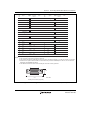
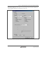
REJ10J1767-0100
SuperH™ Family E10A-USB Multi-core Emulator
Additional Document for User’s Manual
Supplementary Information on Using the SH7265 and
SH7205
Renesas Microcomputer Development Environment System
SuperH™ Family
E10A-USB Multi-core for SH7265 HS7265KCU04HE
Rev.1.00
Revision Date: Nov. 26, 2007
Rev. 1.00 Nov. 26, 2007 Page ii of vi
REJ10J1767-0100
Notes regarding these materials
1. This document is provided for reference purposes only so that Renesas customers may select the appropriate
Renesas products for their use. Renesas neither makes warranties or representations with respect to the
accuracy or completeness of the information contained in this document nor grants any license to any
intellectual property rights or any other rights of Renesas or any third party with respect to the information in
this document.
2. Renesas shall have no liability for damages or infringement of any intellectual property or other rights arising
out of the use of any information in this document, including, but not limited to, product data, diagrams, charts,
programs, algorithms, and application circuit examples.
3. You should not use the products or the technology described in this document for the purpose of military
applications such as the development of weapons of mass destruction or for the purpose of any other military
use. When exporting the products or technology described herein, you should follow the applicable export
control laws and regulations, and procedures required by such laws and regulations.
4. All information included in this document such as product data, diagrams, charts, programs, algorithms, and
application circuit examples, is current as of the date this document is issued. Such information, however, is
subject to change without any prior notice. Before purchasing or using any Renesas products listed in this
document, please confirm the latest product information with a Renesas sales office. Also, please pay regular
and careful attention to additional and different information to be disclosed by Renesas such as that disclosed
through our website. (http://www.renesas.com )
5. Renesas has used reasonable care in compiling the information included in this document, but Renesas
assumes no liability whatsoever for any damages incurred as a result of errors or omissions in the information
included in this document.
6. When using or otherwise relying on the information in this document, you should evaluate the information in
light of the total system before deciding about the applicability of such information to the intended application.
Renesas makes no representations, warranties or guaranties regarding the suitability of its products for any
particular application and specifically disclaims any liability arising out of the application and use of the
information in this document or Renesas products.
7. With the exception of products specified by Renesas as suitable for automobile applications, Renesas
products are not designed, manufactured or tested for applications or otherwise in systems the failure or
malfunction of which may cause a direct threat to human life or create a risk of human injury or which require
especially high quality and reliability such as safety systems, or equipment or systems for transportation and
traffic, healthcare, combustion control, aerospace and aeronautics, nuclear power, or undersea communication
transmission. If you are considering the use of our products for such purposes, please contact a Renesas
sales office beforehand. Renesas shall have no liability for damages arising out of the uses set forth above.
8. Notwithstanding the preceding paragraph, you should not use Renesas products for the purposes listed below:
(1) artificial life support devices or systems
(2) surgical implantations
(3) healthcare intervention (e.g., excision, administration of medication, etc.)
(4) any other purposes that pose a direct threat to human life
Renesas shall have no liability for damages arising out of the uses set forth in the above and purchasers who
elect to use Renesas products in any of the foregoing applications shall indemnify and hold harmless Renesas
Technology Corp., its affiliated companies and their officers, directors, and employees against any and all
damages arising out of such applications.
9. You should use the products described herein within the range specified by Renesas, especially with respect
to the maximum rating, operating supply voltage range, movement power voltage range, heat radiation
characteristics, installation and other product characteristics. Renesas shall have no liability for malfunctions or
damages arising out of the use of Renesas products beyond such specified ranges.
10. Although Renesas endeavors to improve the quality and reliability of its products, IC products have specific
characteristics such as the occurrence of failure at a certain rate and malfunctions under certain use
conditions. Please be sure to implement safety measures to guard against the possibility of physical injury, and
injury or damage caused by fire in the event of the failure of a Renesas product, such as safety design for
hardware and software including but not limited to redundancy, fire control and malfunction prevention,
appropriate treatment for aging degradation or any other applicable measures. Among others, since the
evaluation of microcomputer software alone is very difficult, please evaluate the safety of the final products or
system manufactured by you.
11. In case Renesas products listed in this document are detached from the products to which the Renesas
products are attached or affixed, the risk of accident such as swallowing by infants and small children is very
high. You should implement safety measures so that Renesas products may not be easily detached from your
products. Renesas shall have no liability for damages arising out of such detachment.
12. This document may not be reproduced or duplicated, in any form, in whole or in part, without prior written
approval from Renesas.
13. Please contact a Renesas sales office if you have any questions regarding the information contained in this
document, Renesas semiconductor products, or if you have any other inquiries.
Rev. 1.00 Nov. 26, 2007 Page iii of vi
REJ10J1767-0100
Rev. 1.00 Nov. 26, 2007 Page iv of vi
REJ10J1767-0100
Contents
Section 1 Connecting the Emulator with the User System ..................................1
1.1
1.2
1.3
1.4
1.5
Components of the Emulator ............................................................................................ 1
Connecting the Emulator with the User System ............................................................... 2
Installing the H-UDI Port Connector on the User System ................................................ 3
Pin Assignments of the H-UDI Port Connector ................................................................ 3
Recommended Circuit between the H-UDI Port Connector and the MCU ...................... 6
1.5.1 Recommended Circuit (14-Pin Type) .................................................................. 6
1.5.2 Recommended Circuit (38-Pin Type) .................................................................. 8
Section 2 Software Specifications when Using the SH7265 and SH7205 ..........11
2.1
2.2
2.3
Differences between the MCU and the Emulator ............................................................. 11
Specific Functions for the Emulator when Using the SH7265 and SH7205..................... 17
2.2.1 Event Condition Functions .................................................................................. 17
2.2.2 Trace Functions.................................................................................................... 24
2.2.3 Note on Using the JTAG (H-UDI) Clock (TCK)................................................. 40
2.2.4 Notes on Setting the [Breakpoint] Dialog Box .................................................... 40
2.2.5 Notes on Setting the [Event Condition] Dialog Box and the
BREAKCONDITION_SET Command ............................................................... 40
2.2.6 Performance Measurement Function ................................................................... 41
Notes on SH7265 and SH7205 E10A-USB Multi-core Emulator .................................... 47
Rev. 1.00 Nov. 26, 2007 Page v of vi
REJ10J1767-0100
Rev. 1.00 Nov. 26, 2007 Page vi of vi
REJ10J1767-0100
Section 1 Connecting the Emulator with the User System
Section 1 Connecting the Emulator with the User System
1.1
Components of the Emulator
The E10A-USB Multi core emulator supports the SH7265 and SH7205. Table 1.1 lists the
components of the emulator.
Table 1.1 Components of the Emulator
Classification Component
Hardware
Software
Appearance
Quantity
Remarks
Emulator box
1
HS0005KCU04H:
Depth: 68.0 mm, Width: 101.0 mm,
Height: 22.0 mm, Mass: 73.0 g
User system interface
cable
1
14-pin type:
Length: 20 cm, Mass: 13.0 g
User system interface
cable
1
38-pin type:
Length: 20 cm, Mass: 13.0 g
USB cable
1
Length: 150 cm, Mass: 50.6 g
E10A-USB Multi core
emulator setup program,
TM
SuperH Family E10AUSB Multi-core Emulator
User’s Manual,
Supplementary
Information on Using the
SH7265 and SH7205*,
and Test program manual
for HS0005KCU01H and
HS0005KCU04H
1
HS0005KCU04SR
HS0005KCU04HJ,
HS0005KCU04HE,
HS7265KCU01HJ,
HS7265KCU01HE,
HS0005TM04HJ, and
HS0005TM04HE
(Provided on the CD-R)
Note: Additional document for the MCUs supported by the emulator is included. Check the target
MCU and refer to its additional document.
Rev. 1.00 Nov. 26, 2007 Page 1 of 48
REJ10J1767-0100
Section 1 Connecting the Emulator with the User System
1.2
Connecting the Emulator with the User System
To connect the E10A-USB Multi core emulator (hereinafter referred to as the emulator), the HUDI port connector must be installed on the user system to connect the user system interface
cable. When designing the user system, refer to the recommended circuit between the H-UDI port
connector and the MCU. In addition, read the E10A-USB Multi core emulator user's manual and
hardware manual for the related device.
Table 1.2 shows the type number of the emulator, the corresponding connector type, and the use of
AUD function.
Table 1.2 Type Number, AUD Function, and Connector Type
Type Number
Connector
AUD Function
HS0005KCU04H
14-pin connector
Not Available
HS0005KCU04H
38-pin connector
Available
The H-UDI port connector has the 14-pin and 38-pin types as described below. Use them
according to the purpose of the usage.
1. 14-pin type (without AUD interface)
The H-UDI function is supported. The AUD function is not available.
2. 38-pin type (with AUD interface)
This connector supports AUD tracing, through which a large amount of trace information can
be acquired in realtime. It also supports window tracing, i.e. acquisition of the addresses and
data involved in access to a specified area of memory.
Rev. 1.00 Nov. 26, 2007 Page 2 of 48
REJ10J1767-0100
Section 1 Connecting the Emulator with the User System
1.3
Installing the H-UDI Port Connector on the User System
Table 1.3 shows the recommended H-UDI port connectors for the emulator.
Table 1.3 Recommended H-UDI Port Connectors
Connector
Type Number
Manufacturer
Specifications
14-pin connector
7614-6002
Sumitomo 3M Limited
14-pin straight type
38-pin connector
2-5767004-2
Tyco Electronics AMP K.K.
38-pin Mictor type
Note: If you are using the 14-pin H-UDI connector, do not mount any other component within 3mm of the user-system connector and wiring runs to the MCU. When designing the layout
for the 38-pin connector on the user board, reduce cross-talk noise etc. by keeping other
signal lines out of the region where the H-UDI port connector is situated. As is shown in
figure 1.1, an upper limit (5 mm) applies to the heights of components mounted around the
user system connector.
E10A-USB Multi 38-pin
user system interface cable
30 mm
1
38
2
15 mm
37
2-5767004-2
Target system
5 mm
Area to be kept free of other components
H-UDI port connector
Figure 1.1 Restriction on Component Mounting
1.4
Pin Assignments of the H-UDI Port Connector
Figures 1.2 and 1.3 show the pin assignments of the 14-pin and 38-pin H-UDI port connectors,
respectively.
Note: Note that the pin number assignments of the H-UDI port connector shown on the
following pages differ from those of the connector manufacturer.
Rev. 1.00 Nov. 26, 2007 Page 3 of 48
REJ10J1767-0100
Section 1 Connecting the Emulator with the User System
Pin
No.
1
Input/ *1
Output
Signal
TCK
*2
SH7265
SH7205
Pin No.
Input
J19
Input
K20
2
TRST#
3
TDO
Output
J20
ASEBRKAK#
Input/
L20
/ASEBRK# *2
Output
5
TMS
Input
L19
6
TDI
Input
H20
Output
J17
4
7
RES#
8
N.C.
9
(GND)
11
UVCC
10,12,13
GND
14
GND
*2
Note
User reset
*4
Output
*3
Output
Notes: 1. Input to or output from the user system.
2. The symbol (#) means that the signal is active-low.
3. The emulator monitors the GND signal of the user system and detects whether or not the user system is connected.
4. When the user system interface cable is connected to this pin and the ASEMD# pin is set to 0, do not connect to GND
but to the ASEMD# pin directly.
Pin 1 mark
H-UDI port connector (top view)
25.0
23.0
6 x 2.54 = 15.24
(2.54)
H-UDI port connector (top view)
Pin 8
Pin 14
Pin 1
Pin 7
0.45
Pin 1 mark
Unit: mm
Figure 1.2 Pin Assignments of the H-UDI Port Connector (14 Pins)
Rev. 1.00 Nov. 26, 2007 Page 4 of 48
REJ10J1767-0100
Section 1 Connecting the Emulator with the User System
SH7265
SH7205
Pin No.
Pin
No.
Signal
1
N.C.
20
N.C.
2
N.C.
21
TRST#
Input/ *1
Output
Note
Pin
No.
Signal
*2
Input/ *1
Output
SH7265
SH7205
Pin No.
Input
K20
Output
Y11
Output
W10
Output
Y10
Output
U9
Output
V9
Note
*4
3
ASEMD#(GND)
22
N.C.
4
N.C.
23
N.C.
5
UCON#(GND)
24
AUDATA3
25
N.C.
26
AUDATA2
27
N.C.
28
AUDATA1
29
N.C.
30
AUDATA0
*3
6
AUDCK
7
N.C.
8
ASEBRKAK#/
ASEBRK# *2
9
RES#
10
N.C.
11
Output
W9
Input/
Output
L20
Output
J17
TDO
Output
J20
12
UVCC_AUD
Output
13
N.C.
14
UVCC
15
TCK
16
N.C.
17
TMS
18
N.C.
TDI
19
*2
User reset
Output
Input
Input
Input
J19
L19
H20
31
N.C.
32
AUDSYNC#
33
N.C.
34
N.C.
35
N.C.
36
N.C.
37
N.C.
38
N.C.
Notes: 1. Input to or output from the user system.
2. The symbol (#) means that the signal is active-low.
3. The emulator monitors the GND signal of the user system and detects whether or not the user system is connected.
4. When the user system interface cable is connected to this pin and the ASEMD# pin is set to 0, do not connect to
GND but to the ASEMD# pin directly.
5. The GND bus lead at the center of the H-UDI port connector must be grounded.
37
1
6.91
38
2
25.4
Unit: mm
H-UDI port connector (top view)
Figure 1.3 Pin Assignments of the H-UDI Port Connector (38 Pins)
Rev. 1.00 Nov. 26, 2007 Page 5 of 48
REJ10J1767-0100
Section 1 Connecting the Emulator with the User System
1.5
1.5.1
Recommended Circuit between the H-UDI Port Connector and the
MCU
Recommended Circuit (14-Pin Type)
Figure 1.4 shows a recommended circuit for connection between the H-UDI port connectors (14
pins) and the MCU when the emulator is in use.
Notes: 1. Do not connect anything to the N.C. pins of the H-UDI port connector.
2.
The ASEMD# pin must be 0 when the emulator is connected and 1 when the emulator
is not connected, respectively.
(1) When the emulator is used: ASEMD# = 0
(2) When the emulator is not used: ASEMD# = 1
Figure 1.4 shows an example of circuits that allow the ASEMD# pin to be GND (0)
whenever the emulator is connected by using the user system interface cable.
When the ASEMD# pin is changed by switches, etc., ground pin 9. Do not connect
this pin to the ASEMD# pin.
3.
When a network resistance is used for pull-up, it may be affected by a noise. Separate
TCK from other resistances.
4.
The pattern between the H-UDI port connector and the MCU must be as short as
possible. Do not connect the signal lines to other components on the board.
5.
Since the H-UDI and the AUD of the MCU operate with the PVcc, supply only the
PVcc to the UVCC pin.
6.
The resistance value shown in figure 1.4 is for reference.
7.
The TRST# pin must be at the low level for a certain period when the power is
supplied whether the H-UDI is used or not.
8.
For the pin processing in cases where the emulator is not used, refer to the hardware
manual of the related MCU.
Rev. 1.00 Nov. 26, 2007 Page 6 of 48
REJ10J1767-0100
Section 1 Connecting the Emulator with the User System
PVcc=I/O power supply
All pulled up at 4.7 kΩ
PVcc PVcc PVcc PVcc PVcc
PVcc
H-UDI port connector
(14-pin type)
TCK
9
(GND)
TRST
SH7265, SH7205
1
TCK
2
TRST
3
10 GND
TDO
ASEBRKAK 4
/ASEBRK 5
12
GND
TMS
13
GND
TDI
14 GND
RES
N.C.
UVCC
TDO
ASEBRKAK/ASEBRK
TMS
6
TDI
7
RES
8
11
1kΩ
Reset signal
ASEMD
User system
Figure 1.4 Recommended Circuit for Connection between the H-UDI Port Connector and
MCU when the Emulator is in Use (14-Pin Type)
Rev. 1.00 Nov. 26, 2007 Page 7 of 48
REJ10J1767-0100
Section 1 Connecting the Emulator with the User System
1.5.2
Recommended Circuit (38-Pin Type)
Figure 1.5 shows a recommended circuit for connection between the H-UDI and AUD port
connectors (38 pins) and the MCU when the emulator is in use.
Notes: 1. Do not connect anything to the N.C. pins of the H-UDI port connector.
2.
The ASEMD# pin must be 0 when the emulator is connected and 1 when the emulator
is not connected, respectively.
(1) When the emulator is used: ASEMD# = 0
(2) When the emulator is not used: ASEMD# = 1
Figure 1.5 shows an example of circuits that allow the ASEMD# pin to be GND (0)
whenever the emulator is connected by using the user system interface cable.
When the ASEMD# pin is changed by switches, etc., ground pin 3. Do not connect
this pin to the ASEMD# pin.
3.
When a network resistance is used for pull-up, it may be affected by a noise. Separate
TCK from other resistances.
4.
The pattern between the H-UDI port connector and the MCU must be as short as
possible. Do not connect the signal lines to other components on the board.
5.
The AUD signals (AUDCK, AUDATA3 to AUDATA0, and AUDSYNC#) operate in
high speed. Isometric connection is needed if possible. Do not separate connection nor
connect other signal lines adjacently.
6.
Since the H-UDI and the AUD of the MCU operate with the PVcc, supply only the
PVcc to the UVCC pin.
7.
The resistance value shown in figure 1.5 is for reference.
8.
For the AUDCK pin, guard the pattern between the H-UDI port connector and the
MCU at GND level.
9.
The TRST# pin must be at the low level for a certain period when the power is
supplied whether the H-UDI is used or not.
10. The GND bus lead at the center of the H-UDI port connector must be grounded.
11. For the pin processing in cases where the emulator is not used, refer to the hardware
manual of the related MCU.
Rev. 1.00 Nov. 26, 2007 Page 8 of 48
REJ10J1767-0100
Section 1 Connecting the Emulator with the User System
PVcc=I/O power supply
All pulled-up at 4.7kΩ or more
PVcc
PVcc
PVcc
PVcc
H-UDI port connector
(38-pin type)
AUDCK
AUDSYNC
AUDATA0
SH7265, SH7205
6
AUDCK
32
AUDSYNC
30
AUDATA0
AUDATA1 28
AUDATA1
AUDATA2 26
AUDATA2
AUDATA3 24
AUDATA3
TCK
TMS
TRST
TDI
TDO
ASEBRKAK
/ASEBRK
RES
ASEMD(GND)
UVCC
UVCC_AUD
UCON(GND)
GND
N.C.
15
TCK
17
TMS
21
TRST
19
TDI
11
TDO
8
ASEBRKAK
/ASEBRK
9
RES
3
ASEMD
14
12
1kΩ
Reset signal
5
GND bus leads
1,2,4,7,
10,13,16,18,
20,22,23,25,27,29,
31,33,34,35,36,37,38
User system
Figure 1.5 Recommended Circuit for Connection between the H-UDI Port Connector and
MCU when the Emulator is in Use (38-Pin Type)
Rev. 1.00 Nov. 26, 2007 Page 9 of 48
REJ10J1767-0100
Section 1 Connecting the Emulator with the User System
Rev. 1.00 Nov. 26, 2007 Page 10 of 48
REJ10J1767-0100
Section 2 Software Specifications when Using the SH7265 and SH7205
Section 2 Software Specifications when Using the SH7265
and SH7205
2.1
Differences between the MCU and the Emulator
1. When the emulator system is initiated, it initializes the general registers and part of the control
registers as shown in table 2.1. The initial values of the MCU are undefined. When the
emulator is initiated from the workspace, a value to be entered is saved in a session.
Table 2.1 Register Initial Values at Emulator Link Up
Register
Emulator at Link Up
R0 to R14
H'00000000
R15 (SP)
Value of the SP in the power-on reset vector table
PC
Value of the PC in the power-on reset vector table
SR
H'000000F0
GBR
H'00000000
VBR
H'00000000
TBR
H'00000000
MACH
H'00000000
MACL
H'00000000
PR
H'00000000
FPSCR*
H'00040001
FPUL*
H'00000000
FPR0-15*
H'00000000
Note: If the MCU does not incorporate the floating-point unit (FPU), these registers are not
displayed.
Note: When a value of the interrupt mask bit in the SR register is changed in the [Registers]
window, it is actually reflected in that register immediately before execution of the user
program is started. It also applies when the value is changed by the REGISTER_SET
command.
2. The emulator uses the H-UDI; do not access the H-UDI.
Rev. 1.00 Nov. 26, 2007 Page 11 of 48
REJ10J1767-0100
Section 2 Software Specifications when Using the SH7265 and SH7205
3. Low-Power States
⎯ The single-processor state can be cleared with either the [STOP] button or a break after
satisfaction of the conditions of the Event Condition function, and a break will then occur.
⎯ The dual-sleep state can be cleared with either the [STOP] button or a break after
satisfaction of the conditions of the Event Condition function, and a break will then occur.
⎯ When [Sleep] is selected for [Standby Mode] in the [Configuration] dialog box, the
software standby and deep standby states become the dual-sleep state. Accordingly, the
state can be cleared with either the [STOP] button or a break after satisfaction of the
conditions of the Event Condition function, and a break will then occur.
⎯ When [Standby] is selected for [Standby Mode] in the [Configuration] dialog box, the
software standby and deep standby states transit to their respective standby states, as does
the MCU.
⎯ The memory must not be accessed or modified in the software standby state.
⎯ The memory must not be accessed or modified in the deep standby state.
⎯ When the emulator is in use, the state is in pseudo-deep standby. The operation of registers
whose values are held or updated is the same as in the deep standby state of the MCU.
However, the power is not shut down; only the clock is halted.
⎯ Do not stop the clock input to the H-UDI module by using the module standby function.
4. Reset Signals
The MCU reset signals are only valid in the emulation state while both of CPUs are being
executed. If one of CPUs is in a break state, reset signals are not sent to the MCU.
Note: Do not break the user program when the RES# or WAIT# signal is being low. A
TIMEOUT error will occur. If the WAIT# signal is fixed to low during break, a
TIMEOUT error will occur at memory access.
5. Direct Memory Access Controller (DMAC)
The DMAC operates even when the emulator is used. When a data transfer request is
generated, the DMAC executes DMA transfer.
6. Memory Access during User Program Execution
During execution of the user program, memory is accessed by the following two methods, as
shown in table 2.2; each method offers advantages and disadvantages.
Rev. 1.00 Nov. 26, 2007 Page 12 of 48
REJ10J1767-0100
Section 2 Software Specifications when Using the SH7265 and SH7205
Table 2.2 Memory Access during User Program Execution
Method
Advantage
Disadvantage
H-UDI read/write
The stopping time of the user
program is short because memory
is accessed by the dedicated bus
master.
Cache access is disabled. Actual
memory is always accessed by the
H-UDI read or write.
Short break
Cache access is enabled.
The stopping time of the user
program is long because the user
program temporarily breaks.
Note: Accessing memory to cache control registers 1 and 2 is fixed as a short break during
execution of the user program.
The method for accessing memory during execution of the user program is specified by using
the [Configuration] dialog box.
Table 2.3 Stopping Time by Memory Access (Reference)
Method
Condition
Stopping Time
H-UDI read/write
Reading of one longword for the
internal RAM
Reading: Maximum three bus clocks
(Bφ).
Writing of one longword for the
internal RAM
Writing: Maximum two bus clocks
(Bφ).
CPU clock: 66MHz
About 20ms
Short break
JTAG clock: 5MHz
Reading or writing of one longword
for the external area
7. Memory Access to the External Flash Memory Area
The emulator can download the load module to the external flash memory area (for details,
TM
refer to section 6.22, Download Function to the Flash Memory Area, in the SuperH Family
E10A-USB Multi-core Emulator User’s Manual). Other memory write operations are enabled
for the RAM area. Therefore, an operation such as memory write or BREAKPOINT should be
set only for the RAM area.
Rev. 1.00 Nov. 26, 2007 Page 13 of 48
REJ10J1767-0100
Section 2 Software Specifications when Using the SH7265 and SH7205
8. Operation while Cache is Enabled
When cache is enabled, the emulator operates as shown in table 2.4.
Table 2.4 Operation while Cache is Enabled
Function
Operation
Notes
Memory write
Searches for whether or not the address to be
written hits the instruction and operand caches.
•
The contents of the
address array are not
changed before or
after writing of
memory.
Searches for whether or not the address to be
read hits the operand cache.
•
The instruction cache
is not searched for.
•
When the address hits, the corresponding
position of the data array is read.
•
•
When the address does not hit, single write
is performed to the external area.
The contents of the
address array are not
changed before or
after reading of
memory.
•
Use the Event
Condition if you do not
wish to change the
contents of the
instruction cache.
Memory read
BREAKPOINT
•
When the address hits, the corresponding
position of the data array is changed by the
data to be written and single write is
performed to the external area.
•
When the address does not hit, the cache
contents are not changed and single write is
performed to the external area.
Clears the V and LRU bits of all entries in the
instruction cache to 0 if a BREAKPOINT is set
or canceled.
Clears the V and LRU bits of all entries in the
instruction cache to 0 if a break occurs when a
BREAKPOINT has been set.
Program load
Writes the contents of the data cache to the
external memory and clears the V and LRU bits
of entries in the instruction and data caches to
0 after loading of the program has been
completed. ∗
If memory is read from or written to the disabled cache area, cache is not searched for but the
external area is accessed.
Note: The CPU side which loaded the program operates the above instructions, after completing
the load, however the other which did not load the program will not perform the above
operations even the cache is available. When the updating for the cache is needed, perform
Rev. 1.00 Nov. 26, 2007 Page 14 of 48
REJ10J1767-0100
Section 2 Software Specifications when Using the SH7265 and SH7205
the program load in both of CPU0 side and CPU1 side or flash the cache by operating the
control register for the cache in the CPU which did not the load the program.
9. Multiplexing the AUD Pins
The AUD pins are multiplexed as shown in table 2.5.
Table 2.5 Multiplexed Functions
MCU
Function 1
Function 2
SH7265
SH7205
PJ5/VIDATA0/DACK3#/DACT3#
AUDCK
PJ6/VIDATA1/TEND3#
AUDSYNC#
PJ7/VIDATA2/TIOC1A
AUDATA0
PJ8/VIDATA3/TIOC1B
AUDATA1
PJ9/VIDATA4/SSCK1
AUDATA2
PJ10/VIDATA5/SSI1
AUDATA3
Note: Function 1 can be used when the AUD pins of the device are not connected to the
emulator.
The AUD pins are multiplexed with other pins. When the AUD function is used by the
emulator, AUD pins are used regardless of the settings of the pin function controller (PFC).
10. Using WDT
The WDT0 or WDT1 for the MCU where a break has occurred does not operate during break.
11. Loading Sessions
Information in [JTAG clock] of the [Configuration] dialog box cannot be recovered by loading
sessions. Thus the TCK value will be 5.00 MHz.
Rev. 1.00 Nov. 26, 2007 Page 15 of 48
REJ10J1767-0100
Section 2 Software Specifications when Using the SH7265 and SH7205
12. [IO] Window
⎯ Display and modification
There are two registers to be separately used for write and read operations.
Table 2.6 Register with Different Access Size
Register Name
Usage
Register
WTCSR0(W)
Write
Watchdog timer control/status register
WTCSR1(W)
Write
Watchdog timer control/status register
WTCNT0(W)
Write
Watchdog timer counter
WTCNT1(W)
Write
Watchdog timer counter
WTCSR0(R)
Read
Watchdog timer control/status register
WTCSR1(R)
Read
Watchdog timer control/status register
WTCNT0(R)
Read
Watchdog timer counter
WTCNT1(R)
Read
Watchdog timer counter
WRCSR0(W)
Write
Watchdog reset control/status register
WRCSR1(W)
Write
Watchdog reset control/status register
WRCSR0(R)
Read
Watchdog reset control/status register
WRCSR1(R)
Read
Watchdog reset control/status register
⎯ Customization of the I/O-register definition file
After the I/O-register definition file (SH2A_D1.io) is created, the MCU’s specifications
may be changed. If each I/O register in the I/O-register definition file differs from
addresses described in the hardware manual, change the I/O-register definition file
according to the description in the hardware manual. The I/O-register definition file can be
customized depending on its format. However, the emulator does not support the bit-field
function.
⎯ Verify
In the [IO] window, the verify function of the input value is disabled.
13. Illegal Instructions
Do not execute illegal instructions with STEP-type commands.
Rev. 1.00 Nov. 26, 2007 Page 16 of 48
REJ10J1767-0100
Section 2 Software Specifications when Using the SH7265 and SH7205
14. Reset Input
During execution of the user program, the emulator may not operate correctly if a contention
occurs between the following operations for the emulator and the reset input to the target
device:
⎯ Setting an Event Condition
⎯ Setting an internal trace
⎯ Displaying the content acquired by an internal trace
⎯ Reading or writing of a memory
Note that those operations should not contend with the reset input to the target device.
2.2
2.2.1
Specific Functions for the Emulator when Using the SH7265 and
SH7205
Event Condition Functions
The emulator is used to set event conditions for the following three functions:
• Break of the user program
• Internal trace
• Start or end of performance measurement
The Event Condition functions are common resources for CPU0 or CPU1 and can be set by the
High-performance Embedded Workshop installed in either of the CPUs.
Table 2.7 lists the types of Event Condition.
Rev. 1.00 Nov. 26, 2007 Page 17 of 48
REJ10J1767-0100
Section 2 Software Specifications when Using the SH7265 and SH7205
Table 2.7 Types of Event Condition
Event Condition Type
Description
Address bus condition (Address)
Sets a condition when the address bus (data access) value
or the program counter value (before or after execution of
instructions) is matched.
Data bus condition (Data)
Sets a condition when the data bus value is matched. Byte,
word, or longword can be specified as the access data size.
Bus state condition
(Bus State)
There are two bus state condition settings:
Bus state condition: Sets a condition when the data bus
value is matched.
Read/Write condition: Sets a condition when the read/write
condition is matched.
Count
Sets a condition when the specified other conditions are
satisfied for the specified counts.
CPU core condition
(CPU Core Select)
Sets a condition when the CPU core (CPU0 and CPU1) or
the internal DMA bus (internal DMA write bus and internal
DMA read bus) is accessed.
Reset point
A reset point is set when the count and the sequential
condition are specified.
Action
Selects the operation when a condition (such as a break, a
trace halt condition, or a trace acquisition condition) is
matched.
For a break, the CPU core in which a break will occur is
selected.
Using the [Combination action (Sequential or PtoP)] dialog box, which is opened by selecting
[Combination action (Sequential or PtoP)] from the pop-up menu on the [Event Condition] sheet,
specifies the sequential condition and the start or end of performance measurement.
Table 2.8 lists the combinations of conditions that can be set under Ch1 to Ch11 and the software
trace.
Rev. 1.00 Nov. 26, 2007 Page 18 of 48
REJ10J1767-0100
Section 2 Software Specifications when Using the SH7265 and SH7205
Table 2.8 Dialog Boxes for Setting Event Conditions
Function
Address Bus Data Bus Bus State
Count
CPU Core
Condition
Condition Condition
Condition Condition
(Address)
(Data)
(Bus Status) (Count)
(CPU Select)
Dialog Box
Action
[Event
Condition 1]
Ch1
O
O
O
O
O
(#0, #1, and
DMA)
O
(B, T1, and P1)
[Event
Condition 2]
Ch2
O
O
O
X
O
(#0, #1, and
DMA)
O
(B, T1, and P1)
[Event
Condition 3]
Ch3
O
X
X
X
O
(#0 and #1)
O
(B and T2)
[Event
Condition 4]
Ch4
O
X
X
X
O
(#0 and #1)
O
(B and T3)
[Event
Condition 5]
Ch5
O
X
X
X
O
(#0 and #1)
O
(B and T3)
[Event
Condition 6]
Ch6
O
X
X
X
O
(#0 and #1)
O
(B and T2)
[Event
Condition 7]
Ch7
O
X
X
X
O
(#0 and #1)
O
(B, T2, and P2)
[Event
Condition 8]
Ch8
O
X
X
X
O
(#0 and #1)
O
(B, T2, and P2)
[Event
Condition 9]
Ch9
O
X
X
X
O
(#0 and #1)
O
(B and T2)
[Event
Ch10
Condition 10]
O
X
X
X
O
(#0 and #1)
O
(B and T2)
[Event
Ch11
Condition 11]
O
(reset point)
X
X
X
O
(#0 and #1)
O
(B and T2)
Notes: 1. O: Can be set in the dialog box.
X: Cannot be set in the dialog box.
2. For the CPU Select item,
#0, #1, and DMA: Setting a condition is enabled when CPU0, CPU1, and internal DMA
bus are accessed.
#0 and #1: Setting a condition is enabled when CPU0 and CPU1 are accessed.
Rev. 1.00 Nov. 26, 2007 Page 19 of 48
REJ10J1767-0100
Section 2 Software Specifications when Using the SH7265 and SH7205
3. For the Action item,
B: Setting a break is enabled.
T1: Setting the trace halt and acquisition conditions are enabled for the internal trace.
T2: Setting the trace halt is enabled for the internal trace.
T3: Setting the trace halt and point-to-point is enabled for the internal trace.
P1: Setting a performance-measurement start or end condition is enabled for CPU0.
P2: Setting a performance-measurement start or end condition is enabled for CPU1.
4. The [Event Condition 11] dialog box is used to specify the count of [Event Condition 1]
and becomes a reset point when the sequential condition is specified.
Rev. 1.00 Nov. 26, 2007 Page 20 of 48
REJ10J1767-0100
Section 2 Software Specifications when Using the SH7265 and SH7205
Sequential Setting: Using the [Combination action (Sequential or PtoP)] dialog box specifies the
sequential condition and the start or end of performance measurement.
Table 2.9 Conditions to Be Set
Classification
Item
[Ch1, 2, 3] list box
Sets the sequential condition and the start or end of performance
measurement using Event Conditions 1 to 3 and 11.
Description
Don’t care
Sets no sequential condition or the start or end of
performance measurement.
Break: Ch3-2-1
Breaks when a condition is satisfied in the order of
Event Condition 3, 2, 1.
Break: Ch3-2-1,
Reset point
Breaks when a condition is satisfied in the order of
Event Condition 3, 2, 1.
Enables the reset point of Event Condition 11.
Break: Ch2-1
Breaks when a condition is satisfied in the order of
Event Condition 2, 1.
Break: Ch2-1,
Reset point
Breaks when a condition is satisfied in the order of
Event Condition 2, 1.
Enables the reset point.
I-Trace stop: Ch3-2-1
Halts acquisition of an internal trace when a
condition is satisfied in the order of Event Condition
3, 2, 1.
I-Trace stop: Ch3-2-1, Halts acquisition of an internal trace when a
Reset point
condition is satisfied in the order of Event Condition
3, 2, 1.
Enables the reset point.
I-Trace stop: Ch2-1
Halts acquisition of an internal trace when a
condition is satisfied in the order of Event Condition
2, 1.
I-Trace stop: Ch2-1,
Reset point
Halts acquisition of an internal trace when a
condition is satisfied in the order of Event Condition
2, 1.
Enables the reset point.
Performance: Ch2 to
Ch1 PtoP for CPU0
Sets the performance measurement period for
CPU0 during the time from the satisfaction of the
condition set in Event Condition 2 (start condition)
to the satisfaction of the condition set in Event
Condition 1 (end condition).
Rev. 1.00 Nov. 26, 2007 Page 21 of 48
REJ10J1767-0100
Section 2 Software Specifications when Using the SH7265 and SH7205
Table 2.9 Conditions to Be Set (cont)
Classification
Item
Description
[Ch1, 2, 3] list box
(cont)
Performance: Ch1 to
Ch2 PtoP for CPU0
Sets the performance measurement period for
CPU0 during the time from the satisfaction of the
condition set in Event Condition 1 (start condition)
to the satisfaction of the condition set in Event
Condition 2 (end condition).
[Ch4, 5] list box
Sets the point-to-point of the internal trace (the start or end condition of
trace acquisition) using Event Conditions 4 and 5.
[Ch7, 8] list box
Don’t care
Sets no start or end condition of trace acquisition.
I-Trace: Ch5 to Ch4
PtoP
Sets the acquisition period during the time from the
satisfaction of the condition set in Event Condition
5 (start condition) to the satisfaction of the
condition set in Event Condition 4 (end condition).
I-Trace: Ch5 to Ch4
PtoP, power-on reset
Sets the acquisition period during the time from the
satisfaction of the condition set in Event Condition
5 (start condition) to the satisfaction of the
condition set in Event Condition 4 (end condition)
or the power-on reset.
Sets the start or end of performance measurement using Event Conditions
7 and 8.
Performance: Ch8 to
Ch7 PtoP for CPU1
Sets the performance measurement period for
CPU1 during the time from the satisfaction of the
condition set in Event Condition 8 (start condition)
to the satisfaction of the condition set in Event
Condition 7 (end condition).
Performance: Ch7 to
Ch8 PtoP for CPU1
Sets the performance measurement period for
CPU1 during the time from the satisfaction of the
condition set in Event Condition 7 (start condition)
to the satisfaction of the condition set in Event
Condition 8 (end condition).
Notes: 1. After the sequential condition and the count specification condition of Event Condition 1
have been set, break and trace acquisition will be halted if the sequential condition is
satisfied for the specified count.
2. If a reset point is satisfied, the satisfaction of the condition set in Event Condition will be
disabled. For example, if the condition is satisfied in the order of Event Condition 3, 2,
reset point, 1, the break or trace acquisition will not be halted. If the condition is
satisfied in the order of Event Condition 3, 2, reset point, 3, 2, 1, the break and trace
acquisition will be halted.
3. If the start condition is satisfied after the end condition has been satisfied by measuring
performance, performance measurement will be restarted. For the measurement result
after a break, the measurement results during performance measurement are added.
Rev. 1.00 Nov. 26, 2007 Page 22 of 48
REJ10J1767-0100
Section 2 Software Specifications when Using the SH7265 and SH7205
4. If the start condition is satisfied after the end condition has been satisfied by the pointto-point of the internal trace, trace acquisition will be restarted.
5. When a sequential break is satisfied, the CPU core in which a break will occur is CPU0
or CPU1 specified by the Ch1 condition.
Usage Example of Sequential Break Extension Setting: A tutorial program provided for the
product is used as an example. For the tutorial program, refer to section 6, Tutorial, in the
TM
SuperH Family E10A-USB Multi-core Emulator User’s Manual.
Notes: 1. If the Event condition is set for the slot in the delayed branch instruction by the
program counter (after execution of the instruction), the condition is satisfied before
executing the instruction in the branch destination (when a break has been set, it occurs
before executing the instruction in the branch destination).
2. Do not set the Event condition for the SLEEP instruction by the program counter (after
execution of the instruction).
3. When the Event condition is set for the 32-bit instruction by the program counter, set
that condition in the upper 16 bits of the instruction.
4. If the power-on reset and the Event condition are matched simultaneously, no condition
will be satisfied.
5. Do not set the Event condition for the DIVU or DIVS instruction and the instruction
followed by DIVU and DIVS by the program counter (after execution of the
instruction).
6. If a condition of which intervals are satisfied closely is set, no sequential condition will
be satisfied.
• For the same core, set the Event conditions, which are satisfied closely, by the
program counter with intervals of two or more instructions.
• For the same core, after the data access condition has been matched, set the Event
condition by the program counter with intervals of 17 or more instructions.
7. If the settings of the Event condition or the sequential conditions are changed during
execution of the program, execution will be suspended. (The number of clocks to be
suspended during execution of the program is 102 bus clocks (Bφ). If the bus clock
(Bφ) is 66.6 MHz, the program will be suspended for 1.53 μs.)
8. If the settings of Event conditions or the sequential conditions are changed during
execution of the program, the emulator temporarily disables all Event conditions to
change the settings. During this period, no Event condition will be satisfied.
9. If the break condition before executing an instruction is set to the instruction followed
by DIVU and DIVS, the factor for halting a break will be incorrect under the following
Rev. 1.00 Nov. 26, 2007 Page 23 of 48
REJ10J1767-0100
Section 2 Software Specifications when Using the SH7265 and SH7205
condition:
If a break occurs during execution of the above DIVU and DIVS instructions, the break
condition before executing an instruction, which has been set to the next instruction,
may be displayed as the factor for halting a break.
10. If the break conditions before and after executing instructions are set to the same
address, the factor for halting a break will be incorrectly displayed. The factor for
halting a break due to the break condition after executing an instruction will be
displayed even if a break is halted by the break condition before executing an
instruction.
11. Do not set the break condition after executing instructions and BREAKPOINT
(software break) to the same address.
12. When the emulator is being connected, the user break controller (UBC) function is not
available.
2.2.2
Trace Functions
The emulator supports the trace functions listed in table 2.10.
Table 2.10 Trace Functions
Function
Internal Trace
AUD Trace
Branch trace
Supported
Supported
Memory access trace
Supported
Supported
Software trace
Supported
Supported
Rev. 1.00 Nov. 26, 2007 Page 24 of 48
REJ10J1767-0100
Section 2 Software Specifications when Using the SH7265 and SH7205
Internal Trace Function: When [I-Trace] is selected for [Trace type] on the [Trace Mode] page
of the [Acquisition] dialog box, the internal trace can be used.
Figure 2.1 [Acquisition] Dialog Box – Internal Trace Function
Rev. 1.00 Nov. 26, 2007 Page 25 of 48
REJ10J1767-0100
Section 2 Software Specifications when Using the SH7265 and SH7205
For the internal trace, using [Channel 1] or [Channel 2] of [I-Trace mode] enables acquisition of
512-step trace information on a different bus. When only [Channel 1] is used, 1024-step trace
information can be acquired.
The internal trace functions are common resources for CPU0 or CPU1 and can be set by the Highperformance Embedded Workshop installed in either of the CPUs.
For [Channel 1] and [Channel 2], it is possible to select a bus that acquires trace information
among the items shown in table 2.11.
Table 2.11 Information on Acquiring the Internal Trace
Item*
Acquisition Information
Note
[M-Bus & Branch,
CPU0]
Acquires the data and branch information on the
M-bus for CPU0.
-
•
•
•
•
[I-Bus, CPU0]
Data access (read/write)
PC-relative access
Branch information
Software trace
Acquires the data on the I-bus for CPU0.
-
• Data access (read/write)
• Instruction fetch
[F-Bus, CPU0]
Acquires the data on the F-bus for CPU0.
-
• Instruction fetch
[M-Bus & Branch,
CPU1]
Acquires the data and branch information on the
M-bus for CPU1.
•
•
•
•
[I-Bus, CPU1]
-
Data access (read/write)
PC-relative access
Branch information
Software trace
Acquires the data on the I-bus for CPU1.
-
• Data access (read/write)
• Instruction fetch
[F-Bus, CPU1]
Acquires the data on the F-bus for CPU1.
• Instruction fetch
Rev. 1.00 Nov. 26, 2007 Page 26 of 48
REJ10J1767-0100
-
Section 2 Software Specifications when Using the SH7265 and SH7205
Table 2.11 Information on Acquiring the Internal Trace (cont)
Item*
Acquisition Information
Note
[DMAC]
Acquires the access of the internal DMA bus.
Selected only for
[Channel 1].
• Internal DMA write-bus access
• Internal DMA read-bus access
[None]
Selects no acquisition information; this item is only
set when 1024-step trace information is acquired in
[Channel 1].
Selected only for
[Channel 2].
Note: It is not possible to select the same items for [Channel 1] and [Channel 2].
Acquired information can be selected from the [Acquisition] item for the bus information
specified for [Channel 1] or [Channel 2].
Table 2.12 Acquired Information
Item
Description
M-bus
I-bus
F-bus
Read
Selects acquisition of the read
cycle on the M-bus or I-bus.
Enabled
Enabled
Disabled
Write
Selects acquisition of the write
cycle on the M-bus or I-bus.
Enabled
Enabled
Disabled
PC relative addressing
Selects acquisition of the PCrelative access.
Enabled
Disabled
Disabled
Branch
Selects acquisition of branch
information
Enabled
Disabled
Disabled
Software
Selects acquisition of the software
trace*.
Enabled
Disabled
Disabled
Data access
Selects acquisition of the data
access (read or write) on the Mbus or I-bus.
Enabled
Enabled
Disabled
Instruction Fetch
Acquires instruction fetch from the
external area.
Disabled
Enabled
Enabled
Note: This function is supported with the SHC/C++ compiler (manufactured by Renesas
Technology Corp.) V7.0 or later.
A software trace can be used by describing the Trace(x) function (x is a variable name), which
is compiled and linked, on the C source lines. For details, refer to the SHC manual.
When the load module is downloaded on the emulator and executed while a software trace
function is valid, the PC value that has executed the Trace(x) function, the general register
value for x, and the source lines are displayed.
Rev. 1.00 Nov. 26, 2007 Page 27 of 48
REJ10J1767-0100
Section 2 Software Specifications when Using the SH7265 and SH7205
When the on-chip trace buffer becomes full, the operation is selected through [When trace buffer
full] from the following modes.
Table 2.13 Operation Mode when the On-Chip Trace Buffer Becomes Full
Type
Mode
Description
Acquisition
mode when
the on-chip
trace buffer
becomes full
[Trace continue]
This function overwrites the oldest trace information to store
the latest trace information.
[Trace stop]
After the trace buffer becomes full, the trace information is no
longer acquired. The user program is continuously executed.
[Break]
Breaks the user program.
The contents to be displayed in the [Trace] window can be selected from table 2.15 according to
the [Display Type] item. The [Display Type] item can be set separately by the High-performance
Embedded Workshop for CPU0 and CPU1.
Table 2.14 Contents to be Displayed in the [Trace] Window
Type
Description
[CPU0] check box
Displays the contents including the CPU0 operation among the acquired
trace information.
[CPU1] check box
Displays the contents including the CPU1 operation among the acquired
trace information.
[DMAC] check box
Displays the contents including the DMAC operation among the
acquired trace information.
After selecting [Channel 1] or [Channel 2] of [I-Trace mode], select the content to be acquired
from [Acquisition]. Typical examples are described below (note that items disabled for
[Acquisition] are not acquired).
• Example of acquiring only 1024-step branch information executed in CPU0:
Select [M-Bus & Branch, CPU0] from [Channel 1] and enable [Branch] on [Acquisition].
Select [None] from [Channel 2].
• Example of acquiring only 1024-step read or write access (M-bus) in CPU0 by a user program:
Select [M-Bus & Branch, CPU0] from [Channel 1] and enable [Read], [Write], and [Data
access] on [Acquisition].
Select [None] from [Channel 2].
• Example of acquiring only 1024-step read access by DMA:
Rev. 1.00 Nov. 26, 2007 Page 28 of 48
REJ10J1767-0100
Section 2 Software Specifications when Using the SH7265 and SH7205
Select [DMAC] from [Channel 1] and enable [Read] on [Acquisition].
Select [None] from [Channel 2].
Using Event Condition restricts the condition; the following three items are set as the internal trace
conditions.
Table 2.15 Trace Conditions of the Internal Trace
Item
Acquisition Information
Trace halt
Acquires the internal trace until the Event Condition is satisfied. (The
trace content is displayed in the [Trace] window after a trace has been
halted. No break occurs in the user program.)
Trace acquisition
Acquires only the data access where the Event Condition is satisfied.
Point-to-point
Traces the period from the satisfaction of Event Condition 4 to the
satisfaction of Event Condition 5.
To restrict trace acquisition to access for only a specific address or specific function of a program,
an Event Condition can be used. Typical examples are described below.
• Example of halting a trace with a write access (M-bus) to H’FFF80000 in CPU0 by the user
program as a condition (trace halt):
Set the condition to be acquired on [I-Trace mode].
Set the following in the [Event Condition 1] or [Event Condition 2] dialog box:
Address condition: Set [Address] and H’FFF80000.
Bus state condition: Set [M-Bus] and [Write].
CPU core condition: Set [CPU0].
Action condition: Disable [Acquire Break] and set [Acquire Trace] for [Stop].
• Example of acquiring only write access (M-bus) to H’FFF80000 in CPU0 by the user program
(trace acquisition condition):
Select [M-Bus & Branch, CPU0] from [Channel 1] and enable [Write] and [Data access] on
[Acquisition].
Set the following in the [Event Condition 1] or [Event Condition 2] dialog box:
Address condition: Set [Address] and H’FFF80000.
Bus state condition: Set [M-Bus] and [Write].
CPU core condition: Set [CPU0].
Action condition: Disable [Acquire Break] and set [Acquire Trace] for [Condition].
Rev. 1.00 Nov. 26, 2007 Page 29 of 48
REJ10J1767-0100
Section 2 Software Specifications when Using the SH7265 and SH7205
For the trace acquisition condition, the condition to be acquired by Event Condition should be
acquired by [I-Trace mode].
• Example of acquiring a trace for the period while the user program executed in CPU0 passes
H’1000 through H’2000 (point-to-point):
Set the condition to be acquired on [I-Trace mode].
Set the address condition as H’1000 in the [Event Condition 5] dialog box and the CPU core
condition as [CPU0].
Set the address condition as H’2000 in the [Event Condition 4] dialog box and the CPU core
condition as [CPU0].
Set [I-Trace] as [Ch5 to Ch4 PtoP] in the [Combination action (Sequential or PtoP)] dialog
box.
When point-to-point and trace acquisition condition are set simultaneously, they are ANDed.
Rev. 1.00 Nov. 26, 2007 Page 30 of 48
REJ10J1767-0100
Section 2 Software Specifications when Using the SH7265 and SH7205
Notes on Internal Trace:
• Acquiring internal trace
To acquire the internal trace, both of CPU0 and CPU1 must be in the execution states after the
trace acquisition condition has been set. If execution of one of CPUs is stopped, acquisition of
the internal trace is halted.
• Timestamp
The timestamp is the clock counts of Bφ (48-bit counter). Table 2.17 shows the timing for
acquiring the timestamp.
Table 2.16 Timing for the Timestamp Acquisition
Item
Acquisition Information
Counter Value Stored in the Trace Memory
F-bus fetch
Counter value when a fetch has been completed
M-bus data access
Counter value when data access (read or write) has
been completed
Branch
Counter value when the next bus cycle has been
completed after a branch
I-bus
Fetch
Counter value when a fetch has been completed
Data access
Counter value when data access has been completed
• Point-to-point
The trace-start condition is satisfied when the specified instruction has been fetched.
Accordingly, if the trace-start condition has been set for the overrun-fetched instruction (an
instruction that is not executed although it has been fetched at a branch or transition to an
interrupt), tracing is started during overrun-fetching of the instruction. However, when
overrun-fetching is achieved (a branch is completed), tracing is automatically suspended.
If the start and end conditions are satisfied closely, trace information will not be acquired
correctly.
The execution cycle of the instruction fetched before the start condition is satisfied may be
traced.
When the I-bus is acquired, do not specify point-to-point.
Memory access may not be acquired by the internal trace if it occurs at several instructions
immediately before satisfaction of the point-to-point end condition.
• Halting a trace
Do not set the trace halt condition for the sleep instruction and the branch instruction that the
delay slot becomes the sleep instruction.
Rev. 1.00 Nov. 26, 2007 Page 31 of 48
REJ10J1767-0100
Section 2 Software Specifications when Using the SH7265 and SH7205
• Trace acquisition condition
When [I-Bus, M-Bus & Branch] is selected and the trace acquisition condition is set for the Mbus and I-bus with Event Condition, set the M-bus condition and the I-bus condition for [Event
Condition 1] and [Event Condition 2], respectively.
If the settings of [I-Trace mode] are changed during execution of the program, execution will
be suspended. (The number of clocks to be suspended during execution of the program is the
maximum is around 51 peripheral clock (Pφ)+15 bus clock (Bφ). The program will be
suspended for 1.757μ, when the peripheral clock (Pφ) is 33MHz, the bus clock (Pφ) is
66MHz.)
• Displaying a trace
If a trace is displayed during execution of the program, execution will be suspended to acquire
the trace information. (The number of clocks to be suspended during execution of the program
is the maximum is around 20480 peripheral clock (Pφ)+4096 bus clock (Bφ). The program will
be suspended for 676.52μ, when the peripheral clock (Pφ) is 33.3MHz, the bus clock (Bφ) is
66.6MHz.)
• Branch trace
If breaks occur immediately after executing non-delayed branch and TRAPA instructions and
generating a branch due to exception or interrupt, a trace for one branch will not be acquired
immediately before such breaks.
However, this does not affect on generation of breaks caused by a BREAKPOINT and a break
before executing instructions of Event Condition.
• Writing memory immediately before generating a break
If an instruction is executed to write memory immediately before generating a break, trace
acquisition may not be performed.
Rev. 1.00 Nov. 26, 2007 Page 32 of 48
REJ10J1767-0100
Section 2 Software Specifications when Using the SH7265 and SH7205
AUD Trace Functions: This function is operational when the AUD pin of the device is
connected to the emulator. The AUD trace functions are common resources for CPU0 or CPU1
and can be set by the High-performance Embedded Workshop installed in either of the CPUs.
Table 2.17 shows the AUD trace acquisition mode that can be set in each trace function.
Table 2.17 AUD Trace Acquisition Mode
Type
Mode
Description
Continuous
trace occurs
Realtime trace
When the next branch occurs while the trace information is
being output, all the information may not be output. The user
program can be executed in realtime, but some trace
information will be lost.
Non realtime trace
When the next branch occurs while the trace information is
being output, the CPU stops operations until the information
is output. The user program is not executed in realtime.
Trace continue
This function overwrites the oldest trace information to store
the latest trace information.
Trace stop
After the trace buffer becomes full, the trace information is no
longer acquired. The user program is continuously executed.
Trace buffer
full
The contents to be displayed in the [Trace] window can be selected from table 2.18 according to
the item of [Display Type]. The item of [Display Type] can be set separately by the Highperformance Embedded Workshop for CPU0 and CPU1.
Table 2.18 Contents to be Displayed in the [Trace] Window
Type
Description
[CPU0] check box
Displays the contents including the CPU0 operation among the acquired
trace information.
[CPU1] check box
Displays the contents including the CPU1 operation among the acquired
trace information.
[DMAC] check box
Displays the contents including the DMAC operation among the
acquired trace information.
Rev. 1.00 Nov. 26, 2007 Page 33 of 48
REJ10J1767-0100
Section 2 Software Specifications when Using the SH7265 and SH7205
To set the AUD trace acquisition mode, click the [Trace] window with the right mouse button and
select [Setting] from the pop-up menu to display the [Acquisition] dialog box. The AUD trace
acquisition mode can be set in the [AUD mode1] or [AUD mode2] group box in the [Trace mode]
page of the [Acquisition] dialog box.
Figure 2.2 [Trace mode] Page
Rev. 1.00 Nov. 26, 2007 Page 34 of 48
REJ10J1767-0100
Section 2 Software Specifications when Using the SH7265 and SH7205
When the AUD trace function is used, select the [AUD function] radio button in the [Trace type]
group box of the [Trace mode] page.
Select the [AUD Trace (CPU0)] and [AUD Trace (CPU1)] pages for tracing execution of CPU0
and CPU1, respectively.
(a) Branch Trace Function
The branch source and destination addresses and their source lines are displayed.
[Setting Method]
(i) Select the [AUD Trace (CPU0)] page or the [AUD Trace (CPU1)] page.
(ii) Branch trace can be acquired by selecting the [Branch trace] check box in the [Trace
Settings] group box.
The branch type can be selected in the [Branch trace] group box.
Rev. 1.00 Nov. 26, 2007 Page 35 of 48
REJ10J1767-0100
Section 2 Software Specifications when Using the SH7265 and SH7205
Figure 2.3 Setting Branch Trace in the [AUD Trace (CPU0)] Page
Rev. 1.00 Nov. 26, 2007 Page 36 of 48
REJ10J1767-0100
Section 2 Software Specifications when Using the SH7265 and SH7205
(b) Window Trace Function
Memory access in the specified range can be acquired by trace.
Two memory ranges can be specified for channels A and B. The read, write, or read/write
cycle can be selected as the bus cycle for trace acquisition.
[Setting Method]
(i)
Select the [AUD Trace (CPU0)] page or the [AUD Trace (CPU1)] page.
(ii) Select the [Window trace] check box in the [Trace Settings] group box.
(iii) Select the [Channel A] and [Channel B] check boxes in the [Trace Settings] group box.
Each channel will become valid.
(iv) Specify the bus cycle, memory range, bus type, and bus type to be set for each channel.
Rev. 1.00 Nov. 26, 2007 Page 37 of 48
REJ10J1767-0100
Section 2 Software Specifications when Using the SH7265 and SH7205
Figure 2.4 Setting Window Trace in the [AUD Trace (CPU0)] Page
Note: When [M-Bus] or [DMAC] is selected, the following bus cycles will be traced.
• M-Bus: A bus cycle generated by the CPU is acquired. A bus cycle is also acquired
when the cache has been hit.
• DMAC: A bus cycle generated by the DMA is acquired.
Rev. 1.00 Nov. 26, 2007 Page 38 of 48
REJ10J1767-0100
Section 2 Software Specifications when Using the SH7265 and SH7205
(c) Software Trace Function
Note: This function is supported with SHC/C++ compiler (manufactured by Renesas
Technology Corp.; including OEM and bundle products) V7.0 or later.
A software trace can be used by describing the Trace(x) function (x is a variable name), which
is compiled and linked, on the C source lines. For details, refer to the SHC manual.
When the load module is downloaded on the emulator and is executed while a software trace
function is valid, the PC value that has executed the Trace(x) function, the general register
value for x, and the source lines are displayed.
[Setting Method]
(i)
Select the [AUD Trace (CPU0)] page or the [AUD Trace (CPU1)] page.
(ii) Select the [Software trace] check box in the [Trace Settings] group box.
Notes on AUD Trace:
1. When the trace display is performed during user program execution, the mnemonics, operands,
or source is not displayed.
2. The AUD trace function outputs the differences between newly output branch source addresses
and previously output branch source addresses. The window trace function outputs the
differences between newly output addresses and previously output addresses. If the previous
branch source address is the same as the upper 16 bits, the lower 16 bits are output. If it
matches the upper 24 bits, the lower 8 bits are output. If it matches the upper 28 bits, the lower
4 bits are output.
The emulator regenerates the 32-bit address from these differences and displays it in the
[Trace] window. If the emulator cannot display the 32-bit address, it displays the difference
from the previously displayed 32-bit address.
3. If the 32-bit address cannot be displayed, the source line is not displayed.
4. If a completion-type exception occurs during exception branch acquisition, the next address to
the address in which an exception occurs is acquired.
5. Set the AUD clock (AUDCK) frequency to 50 MHz or lower. If the frequency is higher than
50 MHz, the emulator will not operate normally. The AUD clock can be set in the
[Configuration] dialog box.
6. If breaks occur immediately after executing non-delayed branch and TRAPA instructions and
generating a branch due to exception or interrupt, a trace for one branch will not be acquired
immediately before such breaks. However, this does not affect on generation of breaks caused
by a BREAKPOINT and a break before executing instructions of Event Condition.
Rev. 1.00 Nov. 26, 2007 Page 39 of 48
REJ10J1767-0100
Section 2 Software Specifications when Using the SH7265 and SH7205
2.2.3
Note on Using the JTAG (H-UDI) Clock (TCK)
1. Set the JTAG clock (TCK) frequency to lower than the frequency of the peripheral module
clock.
2. The initial value of the JTAG clock (TCK) is 5.00 MHz.
3. A value to be set for the JTAG clock (TCK) is initialized after executing [Reset CPU] or
[Reset Go]. Thus the TCK value will be 5.00 MHz.
2.2.4
Notes on Setting the [Breakpoint] Dialog Box
1. When an odd address is set, the next lowest even address is used.
2. A BREAKPOINT is accomplished by replacing instructions of the specified address.
It cannot be set to the following addresses:
⎯ An area other than CS and the internal RAM
⎯ An instruction in which Break Condition 2 is satisfied
⎯ A slot instruction of a delayed branch instruction
3. During step operation, specifying BREAKPOINTs and Event Condition breaks are disabled.
4. When execution resumes from the address where a BREAKPOINT is specified and a break
occurs before Event Condition execution, single-step operation is performed at the address
before execution resumes. Therefore, realtime operation cannot be performed.
5. When a BREAKPOINT is set to the slot instruction of a delayed branch instruction, the PC
value becomes an illegal value. Accordingly, do not set a BREAKPOINT to the slot
instruction of a delayed branch instruction.
6. If an address of a BREAKPOINT cannot be correctly set in the ROM or flash memory area, a
mark z will be displayed in the [BP] area of the address on the [Source] or [Disassembly]
window by refreshing the [Memory] window, etc. after Go execution. However, no break will
occur at this address. When the program halts with the event condition, the mark z
disappears.
2.2.5
Notes on Setting the [Event Condition] Dialog Box and the
BREAKCONDITION_SET Command
1. When [Go to cursor], [Step In], [Step Over], or [Step Out] is selected in CPU0, the settings of
Event Condition 3 are disabled.
2. When [Go to cursor], [Step In], [Step Over], or [Step Out] is selected in CPU1, the settings of
Event Condition 5 are disabled.
3. When an Event Condition is satisfied, emulation may stop after two or more instructions have
been executed.
Rev. 1.00 Nov. 26, 2007 Page 40 of 48
REJ10J1767-0100
Section 2 Software Specifications when Using the SH7265 and SH7205
2.2.6
Performance Measurement Function
The emulator supports the performance measurement function.
1. Setting the performance measurement conditions
To set the performance measurement conditions, use the [Performance Analysis] dialog box
and the PERFORMANCE_SET command. When any line in the [Performance Analysis]
window is clicked with the right mouse button, a popup menu is displayed and the
[Performance Analysis] dialog box can be displayed by selecting [Setting].
The performance measurement functions are common resources for CPU0 or CPU1 and can be
set by the High-performance Embedded Workshop installed in either of the CPUs.
Setting channels of the [CPU0] group box measures performance of CPU0. Similarly, setting
channels of the [CPU1] group box measures performance of CPU1.
Note: For the command line syntax, refer to the online help.
Rev. 1.00 Nov. 26, 2007 Page 41 of 48
REJ10J1767-0100
Section 2 Software Specifications when Using the SH7265 and SH7205
(a) Specifying the measurement start/end conditions
For CPU0 performance measurement, the measurement start/end conditions are specified by
using Event Condition 1,2. For CPU1 performance measurement, the measurement start/end
conditions are specified by using Event Condition 7,8. The [Ch1,2,3] and [Ch7,8] list boxes of
the [Combination action (Sequential or PtoP)] dialog box can be used.
Table 2.19 Measurement Period
Classification
Item
Description
Selection in
the [Ch1, 2, 3]
list box
Performance:
Ch2 to Ch1
PtoP for CPU0
For CPU0 performance measurement, the period from the
satisfaction of the condition set in Event Condition 2 (start
condition) to the satisfaction of the condition set in Event
Condition 1 (end condition) is set as the performance
measurement period.
Performance:
Ch1 to Ch2
PtoP for CPU0
For CPU0 performance measurement, the period from the
satisfaction of the condition set in Event Condition 1 (start
condition) to the satisfaction of the condition set in Event
Condition 2 (end condition) is set as the performance
measurement period.
Other than
above
The period from the start of execution of the user program to the
occurrence of a break is measured.
Performance:
Ch8 to Ch7
PtoP for CPU1
For CPU1 performance measurement, the period from the
satisfaction of the condition set in Event Condition 8 (start
condition) to the satisfaction of the condition set in Event
Condition 7 (end condition) is set as the performance
measurement period.
Performance:
Ch7 to Ch8
PtoP for CPU1
For CPU1 performance measurement, the period from the
satisfaction of the condition set in Event Condition 7 (start
condition) to the satisfaction of the condition set in Event
Condition 8 (end condition) is set as the performance
measurement period.
Other than
above
The period from the start of execution of the user program to the
occurrence of a break is measured.
Selection in
the [Ch7, 8]
list box
Rev. 1.00 Nov. 26, 2007 Page 42 of 48
REJ10J1767-0100
Section 2 Software Specifications when Using the SH7265 and SH7205
Figure 2.5 [Performance Analysis] Dialog Box
For measurement tolerance,
• The measured value includes tolerance.
• Tolerance will be generated before or after a break.
Notes: 1. When [Performance: Ch2 to Ch1 PtoP for CPU0] or [Performance: Ch1 to Ch2 PtoP
for CPU0] is selected, to execute the user program, specify conditions set in Event
Condition 2 and Event Condition 1 and one or more items for performance
measurement.
Similarly, when [Performance: Ch8 to Ch7 PtoP for CPU0] or [Performance: Ch7 to
Ch8 PtoP for CPU0] is selected, to execute the user program, specify conditions set in
Event Condition 8 and Event Condition 7 and one or more items for performance
measurement.
Rev. 1.00 Nov. 26, 2007 Page 43 of 48
REJ10J1767-0100
Section 2 Software Specifications when Using the SH7265 and SH7205
2. During user program execution, the change of settings or the measurement items for
the CPU cannot be displayed.
(b) Measurement item
Items are measured by setting channels in the [Performance Analysis] dialog box. A
maximum of eight conditions (four conditions for each of CPU0 and CPU1) can be specified at
the same time.
Rev. 1.00 Nov. 26, 2007 Page 44 of 48
REJ10J1767-0100
Section 2 Software Specifications when Using the SH7265 and SH7205
Table 2.20 Measurement Item
Selected Name
Option
Disabled
None
Elapsed time
AC (The number of execution cycles (Iφ) is set
as the measurement item.)
Branch instruction counts
BT
Number of execution instructions
I
Number of execution 32bit-instructions
I32
Exception/interrupt counts
EA
Interrupt counts
INT
Data cache-miss counts
DC
Instruction cache-miss counts
IC
All area access counts
ARN
All area instruction access counts
ARIN
All area data access counts
ARND
Cacheable area access counts
CDN (data access)
Cacheable area instruction access counts
CIN
Non cacheable area data access counts
NCN
URAM area access counts
UN
URAM area instruction access counts
UIN
URAM area data access counts
UDN
Internal I/O area data access counts
IODN
All area access cycle
ARC
All area instruction access cycle
ARIC
All area data access cycle
ARDC
All area access stall
ARS
All area instruction access stall
ARIS
All area data access stall
ARDS
Note: Selected names are displayed for CONDITION in the [Performance Analysis] window.
Options are parameters for <mode> of the PERFORMANCE_SET command.
Note: In the non-realtime trace mode of the AUD trace, normal counting cannot be performed
because the generation state of the stall or the execution cycle is changed.
Rev. 1.00 Nov. 26, 2007 Page 45 of 48
REJ10J1767-0100
Section 2 Software Specifications when Using the SH7265 and SH7205
2. Displaying the measured result
The measured result is displayed in the [Performance Analysis] window or the
PERFORMANCE_ANALYSIS command with hexadecimal (32 bits).
Note: If a performance counter overflows as a result of measurement, “********” will be
displayed.
3. Initializing the measured result
To initialize the measured result, select [Initialize] from the popup menu in the [Performance
Analysis] window or specify INIT with the PERFORMANCE_ANALYSIS command.
Rev. 1.00 Nov. 26, 2007 Page 46 of 48
REJ10J1767-0100
Section 2 Software Specifications when Using the SH7265 and SH7205
2.3 Notes on SH7265 and SH7205 E10A-USB Multi-core Emulator
Table 2.21 Notes
No.
Function Name
Note
1
The external flash
memory
When using the emulator to program the external flash memory,
break execution by both CPUs beforehand.
2
Memory window
Even when the contents of memory are modified in the memory
window of one High-performance Embedded Workshop, the
contents of the memory window for the other High-performance
Embedded Workshop are not updated automatically. To force
updating in such cases, execute a refresh from the memory
window or issue the command ”REFRESH_2AD” on the
command line. The same applies to other windows which display
the contents of memory; that is, forcible updating is required on
the side where the change was not made.
3
Software break
Do not set the software break to the same address from the Highperformance Embedded Workshop for the CPU0 side and the
one for the CPU1 side.
Do not set the software break at the address of an instruction
which will be executed by both CPU0 and CPU1.
4
Event Condition
Event conditions can be set from the High-performance
Embedded Workshops for both CPU0 and CPU1. When an Event
Condition is modified or added from one High-performance
Embedded Workshop, the [Event] window in the other Highperformance Embedded Workshop is not updated automatically
To force updating in such cases, issue the command
”REFRESH_2AD” on the command line.
Operations on one High-performance Embedded Workshop
should not proceed while the [Event condition] dialog box on the
other the High-performance Embedded Workshop is open. Close
the [Event condition] dialog box before proceeding with
operations on the other the High-performance Embedded
Workshop. When DMA is selected as the bus condition, specify
either Read or Write as the Read and Write conditions (i.e. do not
specify both Read and Write at the same time).
5
Trace
The traces for both CPU0 and CPU1 are being displayed at the
same time (by selecting the buttons for both CPUs in the [Display
type] group box of the [Acquisition] dialog box), do not select
supplementation of branch-trace information.
Rev. 1.00 Nov. 26, 2007 Page 47 of 48
REJ10J1767-0100
Section 2 Software Specifications when Using the SH7265 and SH7205
Table 2.21 Notes (cont)
No.
Function Name
Note
6
Performance
Performance settings can be made from the Highperformance Embedded Workshop for both CPU0 and CPU1.
When performance settings are updated by one Highperformance Embedded Workshop, the performance window
on the other High-performance Embedded Workshop will not
be updated automatically. To update the window, issue the
command ”REFRESH_2AD” on the command line.
7
Memory access
during execution of
the user program
If a break has been generated for one CPU at a time when
execution of the other CPU should be temporarily suspended
(by a short break) for memory access, execution of the CPU
may continue despite generation of the short break. To force
updating in such cases, issue the command
”REFRESH_2AD” on the command line.
Rev. 1.00 Nov. 26, 2007 Page 48 of 48
REJ10J1767-0100
SuperH™ Family E10A-USB Multi-core Emulator
Additional Document for User's Manual
Supplementary Information on Using the SH7265 and SH7205
Publication Date: Rev.1.00, November 26, 2007
Published by:
Sales Strategic Planning Div.
Renesas Technology Corp.
Edited by:
Customer Support Department
Global Strategic Communication Div.
Renesas Solutions Corp.
© 2007. Renesas Technology Corp., All rights reserved. Printed in Japan.
Sales Strategic Planning Div.
Nippon Bldg., 2-6-2, Ohte-machi, Chiyoda-ku, Tokyo 100-0004, Japan
RENESAS SALES OFFICES
http://www.renesas.com
Refer to "http://www.renesas.com/en/network" for the latest and detailed information.
Renesas Technology America, Inc.
450 Holger Way, San Jose, CA 95134-1368, U.S.A
Tel: <1> (408) 382-7500, Fax: <1> (408) 382-7501
Renesas Technology Europe Limited
Dukes Meadow, Millboard Road, Bourne End, Buckinghamshire, SL8 5FH, U.K.
Tel: <44> (1628) 585-100, Fax: <44> (1628) 585-900
Renesas Technology (Shanghai) Co., Ltd.
Unit 204, 205, AZIACenter, No.1233 Lujiazui Ring Rd, Pudong District, Shanghai, China 200120
Tel: <86> (21) 5877-1818, Fax: <86> (21) 6887-7898
Renesas Technology Hong Kong Ltd.
7th Floor, North Tower, World Finance Centre, Harbour City, 1 Canton Road, Tsimshatsui, Kowloon, Hong Kong
Tel: <852> 2265-6688, Fax: <852> 2730-6071
Renesas Technology Taiwan Co., Ltd.
10th Floor, No.99, Fushing North Road, Taipei, Taiwan
Tel: <886> (2) 2715-2888, Fax: <886> (2) 2713-2999
Renesas Technology Singapore Pte. Ltd.
1 Harbour Front Avenue, #06-10, Keppel Bay Tower, Singapore 098632
Tel: <65> 6213-0200, Fax: <65> 6278-8001
Renesas Technology Korea Co., Ltd.
Kukje Center Bldg. 18th Fl., 191, 2-ka, Hangang-ro, Yongsan-ku, Seoul 140-702, Korea
Tel: <82> (2) 796-3115, Fax: <82> (2) 796-2145
Renesas Technology Malaysia Sdn. Bhd
Unit 906, Block B, Menara Amcorp, Amcorp Trade Centre, No.18, Jalan Persiaran Barat, 46050 Petaling Jaya, Selangor Darul Ehsan, Malaysia
Tel: <603> 7955-9390, Fax: <603> 7955-9510
Colophon 6.0
SuperH™ Family E10A-USB
Multi-core Emulator
Additional Document for User’s Manual
Supplementary Information on
Using the SH7265 and SH7205