1
CYUSB3KIT-003
SuperSpeed Explorer Kit User Guide
Doc. # 001-93186 Rev. *A
Cypress Semiconductor
198 Champion Court
San Jose, CA 95134-1709
Phone (USA): 800.858.1810
Phone (Intnl): +1.408.943.2600
http://www.cypress.com
Copyrights
© Cypress Semiconductor Corporation, 2014. The information contained herein is subject to change without notice. Cypress
Semiconductor Corporation assumes no responsibility for the use of any circuitry other than circuitry embodied in a Cypress
product. Nor does it convey or imply any license under patent or other rights. Cypress products are not warranted nor
intended to be used for medical, life support, life saving, critical control or safety applications, unless pursuant to an express
written agreement with Cypress. Furthermore, Cypress does not authorize its products for use as critical components in lifesupport systems where a malfunction or failure may reasonably be expected to result in significant injury to the user. The
inclusion of Cypress products in life-support systems application implies that the manufacturer assumes all risk of such use
and in doing so indemnifies Cypress against all charges.
Any Source Code (software and/or firmware) is owned by Cypress Semiconductor Corporation (Cypress) and is protected by
and subject to worldwide patent protection (United States and foreign), United States copyright laws and international treaty
provisions. Cypress hereby grants to licensee a personal, non-exclusive, non-transferable license to copy, use, modify, create
derivative works of, and compile the Cypress Source Code and derivative works for the sole purpose of creating custom software and or firmware in support of licensee product to be used only in conjunction with a Cypress integrated circuit as specified in the applicable agreement. Any reproduction, modification, translation, compilation, or representation of this Source
Code except as specified above is prohibited without the express written permission of Cypress.
Disclaimer: CYPRESS MAKES NO WARRANTY OF ANY KIND, EXPRESS OR IMPLIED, WITH REGARD TO THIS MATERIAL, INCLUDING, BUT NOT LIMITED TO, THE IMPLIED WARRANTIES OF MERCHANTABILITY AND FITNESS FOR A
PARTICULAR PURPOSE. Cypress reserves the right to make changes without further notice to the materials described
herein. Cypress does not assume any liability arising out of the application or use of any product or circuit described herein.
Cypress does not authorize its products for use as critical components in life-support systems where a malfunction or failure
may reasonably be expected to result in significant injury to the user. The inclusion of Cypress’ product in a life-support systems application implies that the manufacturer assumes all risk of such use and in doing so indemnifies Cypress against all
charges.
Use may be limited by and subject to the applicable Cypress software license agreement.
All trademarks or registered trademarks referenced herein are property of the respective corporations.
Flash Code Protection
Cypress products meet the specifications contained in their particular Cypress PSoC Datasheets. Cypress believes that its
family of PSoC products is one of the most secure families of its kind on the market today, regardless of how they are used.
There may be methods, unknown to Cypress, that can breach the code protection features. Any of these methods, to our
knowledge, would be dishonest and possibly illegal. Neither Cypress nor any other semiconductor manufacturer can guarantee the security of their code. Code protection does not mean that we are guaranteeing the product as ‘unbreakable’.
Cypress is willing to work with the customer who is concerned about the integrity of their code. Code protection is constantly
evolving. We at Cypress are committed to continuously improving the code protection features of our products.
CYUSB3KIT-003 SuperSpeed Explorer Kit User Guide, Doc. # 001-93186 Rev. *A
2
Contents
Safety Information
5
Regulatory Compliance ...............................................................................................5
General Safety Instructions .........................................................................................6
ESD Protection.................................................................................................6
Handling Boards...............................................................................................6
1. Introduction
1.1
1.2
1.3
1.4
1.5
Kit Contents .................................................................................................................7
1.1.1 Software ...........................................................................................................7
1.1.2 Tools Not Included............................................................................................8
1.1.3 Other Suggested Tools.....................................................................................8
Additional Learning Resources....................................................................................8
Documentation Conventions........................................................................................9
Acronyms.....................................................................................................................9
Document History ......................................................................................................10
2. Software Installation
2.1
2.2
2.3
2.4
2.5
2.6
3.6
3.7
11
FX3 SDK Installation on Windows OS .......................................................................11
Rolling Back to a Previous Version of FX3 SDK........................................................12
FX3 SDK Installation on Linux OS.............................................................................12
SuperSpeed Explorer Kit Installation .........................................................................13
Cypress Update Manager ..........................................................................................15
EZ USB Suite (Eclipse) IDE.......................................................................................15
2.6.1 Starting the EZ USB Suite..............................................................................15
2.6.2 Importing a Project .........................................................................................16
2.6.3 Automatically Saving Your Edits.....................................................................18
2.6.4 Building the Project ........................................................................................19
3. Kit Operation
3.1
3.2
3.3
3.4
3.5
7
20
USB Connectors ........................................................................................................20
Jumpers .....................................................................................................................21
Power Mode...............................................................................................................22
USB Control Center ...................................................................................................22
Boot Options ..............................................................................................................23
3.5.1 Boot From Onboard I2C EEPROM ................................................................23
3.5.2 Boot as a USB Loader ...................................................................................26
3.5.3 Program the EEPROM...................................................................................28
Firmware Examples ...................................................................................................29
3.6.1 USBBulkSourceSink with LED Blink ..............................................................29
3.6.2 SRAM Example..............................................................................................30
Integrated Debugger..................................................................................................33
3.7.1 UART .............................................................................................................34
CYUSB3KIT-003 SuperSpeed Explorer Kit User Guide, Doc. # 001-93186 Rev. *A
3
Contents
3.7.2
JTAG ..............................................................................................................36
4. Hardware
4.1
4.2
4.3
4.4
4.5
4.6
46
Power Supply.............................................................................................................46
USB 3.0 Receptacle Connector .................................................................................47
FX3 Clock ..................................................................................................................47
GPIF II Connector......................................................................................................48
4.4.1 SuperSpeed Explorer Kit Interconnect Boards...............................................49
Reset Circuit ..............................................................................................................49
Serial Interfaces.........................................................................................................50
4.6.1 I2C..................................................................................................................50
4.6.2 I2S..................................................................................................................50
4.6.3 SPI and UART................................................................................................50
4.6.4 JTAG ..............................................................................................................51
4.6.5 User Push Button (SW2)................................................................................51
4.6.6 User LED (LED2) ...........................................................................................51
Appendix
52
Troubleshooting ..................................................................................................................52
Manual Installation of a Cypress Driver ....................................................................52
If You Have "Too Many" COM Ports ...................................................................................54
CYUSB3KIT-003 SuperSpeed Explorer Kit User Guide, Doc. # 001-93186 Rev. *A
4
Safety Information
Regulatory Compliance
The CYUSB3KIT-003 SuperSpeed Explorer kit is intended for use as a development platform for hardware or
software in a laboratory environment. The board is an open-system design, which does not include a shielded
enclosure. This kit may cause interference to other electrical or electronic devices in close proximity. In a
domestic environment, this product may cause radio interference. In such cases, take adequate preventive
measures. Also, do not use this board near any medical equipment or RF devices.
Attaching additional wiring to this product or modifying the product operation from the factory default may affect
its performance and cause interference with other apparatus in the immediate vicinity. If such interference is
detected, suitable mitigating measures must be taken.
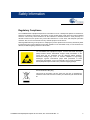
The CYUSB3KIT-003 SuperSpeed Explorer contains electrostatic discharge
(ESD) sensitive devices. Electrostatic charges readily accumulate on the
human body and any equipment, and can discharge without detection.
Permanent damage may occur on devices subjected to high-energy
discharges. Cypress recommends proper ESD precautions to avoid
performance degradation or loss of functionality. Store unused CYUSB3KIT003 SuperSpeed Explorer boards in the protective shipping package.
End-of-Life/Product Recycling
This kit has an end-of-life cycle five years from the year of manufacturing
mentioned on the back of the box. Contact your nearest recycler to discard the
kit.
CYUSB3KIT-003 SuperSpeed Explorer Kit User Guide, Doc. # 001-93186 Rev. *A
5
Safety Information
General Safety Instructions
ESD Protection
ESD can damage boards and associated components. Cypress recommends that you perform procedures only
at an ESD workstation. If an ESD workstation is not available, use appropriate ESD protection by wearing an
antistatic wrist strap attached to the chassis ground (any unpainted metal surface) on the board when handling
parts.
Handling Boards
CYUSB3KIT-003 boards are sensitive to ESD. Hold the board only by its edges. After removing the board from
its box, place it on a grounded, static-free surface. Use a conductive foam pad if available. Do not slide the
board over any surface.
CYUSB3KIT-003 SuperSpeed Explorer Kit User Guide, Doc. # 001-93186 Rev. *A
6
1.
Introduction
Cypress EZ-USB® FX3™ (FX3) is an ARM-based controller designed to implement USB 3.0
peripherals. USB 3.0 offers the SuperSpeed signaling rate of 5 gigabits per second, which is 10
times greater than the high-speed signaling rate of 480 megabits per second. Because FX3 is
USB 3.0 compliant, in addition to operating at the new SuperSpeed data rate, it can also operate at
the High-Speed and Full-Speed USB data rates.
FX3 has a fully configurable General Programmable Interface (GPIF™ II) that can interface with any
processor, ASIC, image sensor, or field-programmable gate array (FPGA). It provides easy and
glueless connectivity to popular industry interfaces such as synchronous slave FIFO, asynchronous
SRAM, asynchronous and synchronous address data multiplexed interfaces, image sensor
interfaces, and CompactFlash. Additionally, users can define proprietary interfaces using Cypress's
GPIF II Designer tool, which is packaged with the FX3 Software Development Kit (SDK).
The SuperSpeed Explorer Kit combines hardware, software, and documentation that enable
customers to evaluate the FX3 device. This user guide describes the steps to install the software
required by the SuperSpeed Explorer Kit and to operate the development board provided with the kit.
The guide also documents different types of firmware download and debug methods with detailed
instructions. Two example projects (USBBulkSourceSinkLED and SRAM_FX3) explain the use of
various features provided on the SuperSpeed Explorer Kit development board and the host
applications provided with the FX3 SDK. This document also explains the hardware interfaces
available on the development board.
Interconnect boards are available to interface the SuperSpeed Explorer Kit development board with
Aptina image sensor boards, Xilinx FPGA boards, and Altera FPGA boards. See Section 4.4.1 on
page 49 for more information on the interconnect boards.
1.1
Kit Contents
The SuperSpeed Explorer Kit contains the following:
■
FX3 development board
■
USB 3.0 A to B cable
■
Quick start guide
■
Jumpers
Visit the kit web page (www.cypress.com/go/SuperSpeedExplorerKit) for more information. Inspect
the contents of the kit. If any parts are missing, contact your nearest Cypress sales office for further
assistance.
1.1.1
Software
FX3 Software Development Kit (FX3 SDK):
The FX3 software development platform is based on the Eclipse integrated development environment (IDE). A prerequisite for using the SuperSpeed Explorer Kit is to download and install the FX3
Software Development Kit (www.cypress.com/go/FX3SDK). This package installs the EZ USB Suite
CYUSB3KIT-003 SuperSpeed Explorer Kit User Guide, Doc. # 001-93186 Rev. *A
7
Introduction
and ARM GCC toolchain, a firmware library with example projects, and the Cypress USB Suite,
including a Windows driver and sample Microsoft Visual Studio applications. After installation, the
Cypress Update Manager ensures that all modules are up to date.
SuperSpeed Explorer Kit Installer:
The SuperSpeed Explorer Kit (www.cypress.com/go/SuperSpeedExplorerKit) installer package
installs documentation (such as user guide, quick start guide, and release notes), hardware files
(such as schematic, PCB layout, and gerber), and firmware examples (USBBulkSourceSinkLED and
SRAM_FX3). The SuperSpeed Explorer Kit installer also includes Windows drivers for FX3 and software for JTAG debugging, including an OpenOCD executable and configuration file to use the
CY7C65215 - USB-Serial Dual Channel Bridge with CapSense® and BCD (www.cypress.com/go/
CY7C65215) on the SuperSpeed Explorer Kit development board as an integrated debugger for
FX3.
1.1.2
1.1.3
Tools Not Included
■
Microsoft Visual C++ or C# software required for editing and building the USB PC application
source code. Free Visual Studio Express editions are available on the Microsoft website.
■
USB 3.0 capable PC host: The SuperSpeed Explorer Kit firmware examples can operate at either
USB 2.0 or USB 3.0 speeds. To achieve maximum performance with the FX3 hardware, use a
PC with a USB 3.0 host controller.
■
Java Runtime Environment (JRE).
Other Suggested Tools
The following USB protocol analyzers can be used to analyze the traffic between the PC host and
the FX3 device:
■
■
1.2
Hardware analyzers
❐
Ellisys USB Explorer 280
❐
Lecroy USB Voyager M3i
❐
Beagle USB 5000 SuperSpeed Protocol Analyzer
Software protocol analyzers
❐
SourceQuest SourceUSB
❐
SysNucleus USBTrace
❐
USBlyzer
Additional Learning Resources
Visit the EZ-USB FX3 web page (www.cypress.com/fx3/) for additional learning resources in the
form of a datasheet, a technical reference manual, application notes, knowledge base articles, and
training videos.
CYUSB3KIT-003 SuperSpeed Explorer Kit User Guide, Doc. # 001-93186 Rev. *A
8
Introduction
1.3
Documentation Conventions
Table 1-1. Document Conventions for Guides
Convention
1.4
Usage
Courier New
Displays file locations, user entered text, and source code:
C:\ ...cd\icc\
Italics
Displays file names and reference documentation.
For example, CYUSBS232UART.cyusb.
[Bracketed, Bold]
Displays keyboard commands in procedures:
[Enter] or [Ctrl] [C]
File > Open
Represents menu paths:
File > Open > New Project
Bold
Displays commands, menu paths, and icon names in procedures:
Click the File icon and then click Open.
Times New Roman
Displays an equation:
2+2=4
Text in gray boxes
Describes cautions or unique functionality of the product.
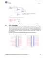
Acronyms
The following table lists the acronyms used in this kit guide.
Acronym
Meaning
AC
Alternating current
ADMUX
Address data multiplexing
API
Application programming interface
ASIC
Application-specific integrated circuit
COM
Communication port
CTS
UART clear to send
DC
Direct current
DSP
Digital signal processor
DVK
Development kit
EEPROM
Electrically erasable programmable read-only memory
EP
Endpoint
ESD
Electrostatic discharge
FMC
FPGA mezzanine c ard
FPGA
Field-programmable gate array
Gbps
Gigabits per second
GCC
GNU compiler collection
GDB
GNU debugger
GPIF
General Programmable Interface
GPIO
General- purpose input/output
HSMC
High-speed mezzanine card
I
2C
I 2S
IDE
Inter-integrated circuit
Inter-IC sound
Integrated development environment
CYUSB3KIT-003 SuperSpeed Explorer Kit User Guide, Doc. # 001-93186 Rev. *A
9
Introduction
Acronym
1.5
Meaning
JTAG
Joint Test Action Group
KB
Kilobyte
LED
Light-emitting diode
MB
Megabyte
Mbps
Megabits per second
OS
Operating system
OTG
On-the-go
PC
Personal computer
PCB
Printed circuit board
PHY
Physical layer
PID
Product ID
RTOS
Real-time operating system
RTS
UART ready to send
SCB
Serial communication block
SCL
I2C serial clock line
SDA
SDK
I2C serial data line
Software development kit
SPI
Serial peripheral interface
USB
Universal serial bus
USB-IF
Universal Serial Bus Implementers’ Forum
VID
Vendor ID
Document History
Revision
PDF Creation
Date
Origin of
Change
Description of Change
**
07/10/2014
NIKL
Initial version of kit user guide.
*A
08/01/2014
NIKL
Updated links. Minor content edits throughout the document.
CYUSB3KIT-003 SuperSpeed Explorer Kit User Guide, Doc. # 001-93186 Rev. *A
10
2.
Software Installation
This chapter guides you through the installation of the FX3 SDK for the Windows and Linux environments and the SuperSpeed Explorer Kit setup for the Windows environment.
Note The SuperSpeed Explorer Kit Quick Start Guide, packaged with the kit box, specifies to download and install the SuperSpeed Explorer Kit Setup as the first step. If this step was followed, the
FX3 SDK and SuperSpeed Explorer Kit Setup are already installed on your machine. You can jump
to Section 2.5 on page 15 for steps to launch Cypress Update Manager. Cypress Update Manager
helps ensure you have the latest FX3 SDK and the SuperSpeed Explorer Kit Setup installed on your
machine.
2.1
FX3 SDK Installation on Windows OS
To install the latest version of the FX3 SDK, follow these steps:
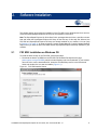
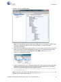
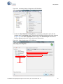
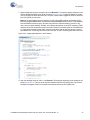
1. Download the latest FX3 SDK from the EZ-USB FX3 Software Development Kit page
(www.cypress.com/go/FX3SDK), which includes Windows and Linux downloads. If your browser
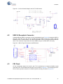
does not ask to run the downloaded file, locate the FX3SDKSetup.exe file in the Downloads
folder and double-click it to start the installer (Figure 2-1).
Figure 2-1. FX3 SDK Installer Screen
CYUSB3KIT-003 SuperSpeed Explorer Kit User Guide, Doc. # 001-93186 Rev. *A
11
Software Installation
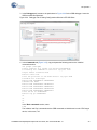
2. Click Next to start the Installation Wizard.
3. Accept the license agreements for the various software components and click Next. The installer
indicates the completion progress (Figure 2-2).
Figure 2-2. Installation Progress Showing Individual Modules
2.2
Rolling Back to a Previous Version of FX3 SDK
Some features or application programming interfaces (APIs) of the SDK may not be supported in the
latest version of the FX3 SDK. To use those features, you can roll back to any previous version of the
FX3 SDK using the Cypress Update Manager. Follow the steps given in the knowledge base article,
How to Roll Back to a Previous Version of FX3 SDK - KBA89637 (www.cypress.com/go/KBA89637),
to install any previous version.
2.3
FX3 SDK Installation on Linux OS
FX3 SDK version 1.2 and later revisions support firmware development with the EZ USB Suite on
the Linux platform. The EZ-USB FX3 SDK (www.cypress.com/go/FX3SDK) for Linux is released in
the form of a gzipped tar archive called "FX3_SDK.tar.gz”. On extraction, this tar archive contains the
following gzipped tar archives:
■
FX3_Firmware.tar.gz: FX3 firmware library and examples
■
ARM_GCC.tgz: Sourcery ARM GNU toolchain to compile firmware examples
■
eclipse_x86.tgz: EZ USB Suite for 32-bit Linux OS
■
eclipse_x64.tgz: EZ USB Suite for 64-bit Linux OS
■
cyusb_linux_<Build_no>.tar.gz: The CyUSB Suite provides QT-based USB applications to communicate with the FX3 device
CYUSB3KIT-003 SuperSpeed Explorer Kit User Guide, Doc. # 001-93186 Rev. *A
12
Software Installation
The installation procedure involves extracting these archives and setting environment variables.
Refer to the FX3_SDK_Linux_Support.pdf file available in the following extracted folder of the FX3
SDK for Linux installation: fx3_sdk_v1.3_linux\FX3_Firmware\cyfx3sdk\doc.
2.4
SuperSpeed Explorer Kit Installation
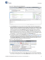
To install the SuperSpeed Explorer Kit software, follow these steps:
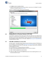
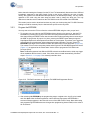
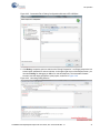
1. Download the latest kit installer from www.cypress.com/go/SuperSpeedExplorerKit. Locate the
SuperSpeedExplorerKitSetup.exe file in the Downloads folder and double-click it to run the
Installer (Figure 2-3).
Figure 2-3. SuperSpeed Explorer Kit Installer Screen
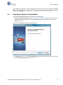
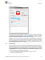
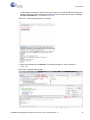
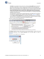
2. Click Next and select the required Installation Type. When installing for the first time, it is best to
select the Typical installation type (Figure 2-4).
CYUSB3KIT-003 SuperSpeed Explorer Kit User Guide, Doc. # 001-93186 Rev. *A
13
Software Installation
Figure 2-4. SuperSpeed Explorer Kit Setup Installation Type Selection
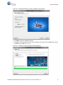
3. Click Next to start the Installation Wizard.
4. Accept the license agreements for the various software components and click Next. Wait until the
installation is complete (Figure 2-5).
Figure 2-5. Installation Progress Showing Individual Modules
CYUSB3KIT-003 SuperSpeed Explorer Kit User Guide, Doc. # 001-93186 Rev. *A
14
Software Installation
2.5
Cypress Update Manager
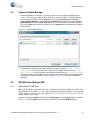
1. When the installation is complete, you have the option to run the Cypress Update Manager
(Figure 2-6) to ensure you have the latest Explorer Kit revision installed. The Update Manager
can be launched in Windows from the Start menu by choosing All Programs > Cypress >
Cypress Update Manager. Click the Check for updates button at the bottom of the Cypress
Update Manager window. If No Updates appear next to the FX3 SDK or SuperSpeed Explorer
Kit, click the Exit button. If there are updates, click the Update button to download and install the
latest software.
Figure 2-6. Cypress Update Manager
2. The installation creates the SuperSpeed Explorer Kit folder in the path <Install Directory>\Cypress (note that for Windows 7 and above, the default install directory is C:\Program Files (x86)and for Windows XP, the default install directory is C:\Program Files).
This folder contains documentation, drivers, hardware files, example firmware, and an OpenOCD
executable for using the USB-Serial IC (www.cypress.com/go/CY7C65215) as a USB-JTAG
debugger.
2.6
EZ USB Suite (Eclipse) IDE
2.6.1
Starting the EZ USB Suite
Note The EZ USB Suite is dependent on the Java Runtime Environment (JRE). As the JRE is not
packaged with the FX3 SDK 1.3.1, you need to download and install it separately. You can get the
current version of Java from the Java website (http://java.com/en/download/index.jsp) if it is not
already installed on the system.
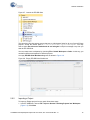
Navigate to the Windows Start menu and select All Programs; click the Cypress folder to expand it
(Figure 2-7). Click the Eclipse entry to expand it and double-click the EZ USB Suite entry.
CYUSB3KIT-003 SuperSpeed Explorer Kit User Guide, Doc. # 001-93186 Rev. *A
15
Software Installation
Figure 2-7. Launch the EZ USB Suite
This launches a first-time startup screen that sets up a Workspace folder for all your Cypress Eclipse
projects. Accept the default path of C:\Users\(username)\Cypress\Workspace. You may
want to select Use this as the default and do not ask again to skip this message every time you
start the EZ USB Suite.
You can create more workspaces by choosing File > Switch Workspace > Other. In this way, you
can define different workspaces for different projects.
An empty EZ USB Suite Workbench appears as shown in Figure 2-8.
Figure 2-8. Empty EZ USB Suite Workbench
2.6.2
Importing a Project
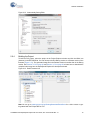
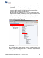
To import an Eclipse project from any path, follow these steps.
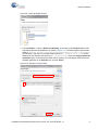
1. In the EZ USB Suite, choose File > Import > General > Existing Projects into Workspace
(Figure 2-9). Click Next.
CYUSB3KIT-003 SuperSpeed Explorer Kit User Guide, Doc. # 001-93186 Rev. *A
16
Software Installation
Figure 2-9. Import an Eclipse Project
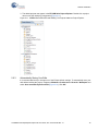
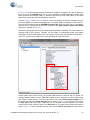
2. Click the Browse… button to Select root directory: and browse to the Firmware folder of the
SuperSpeed Explorer Kit installation, as shown in Figure 2-10. The default path to the firmware
folder is <Install Directory>\Cypress\SuperSpeed Explorer Kit\1.0\Firmware
(for Windows 7 and above, the default install directory is C:\Program Files (x86)and for
Windows XP, the default install directory is C:\Program Files). Select the Copy projects into
workspace option so that the project folder will be copied to your Workspace folder. Select the
firmware application in the Projects: box, and click Finish.
Figure 2-10. Browse to Project Folder
CYUSB3KIT-003 SuperSpeed Explorer Kit User Guide, Doc. # 001-93186 Rev. *A
17
Software Installation
3. The added projects now appear in the EZ USB Suite Project Explorer. Double-click a project
name to see the underlying components (Figure 2-11).
Figure 2-11. USBBulkSourceSinkLED and SRAM_FX3 Projects Added to Project Explorer
2.6.3
Automatically Saving Your Edits
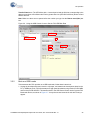
It is recommended that you change one of the Eclipse default settings. To automatically save your
edits before building the project, navigate to Windows > Preferences > General > Workspace and
select Save automatically before build (Figure 2-12). Click OK.
CYUSB3KIT-003 SuperSpeed Explorer Kit User Guide, Doc. # 001-93186 Rev. *A
18
Software Installation
Figure 2-12. Automatically Saving Edits
2.6.4
Building the Project
To build an FX3 project, select the project in the Project Explorer window and click the Build icon
(hammer) in the EZ USB Suite. You can choose to build a Debug version or a Release version of the
firmware (Figure 2-13). The generated image file in the Release version is smaller than in the Debug
version. See Section 3.5.2 on page 26 and Section 3.5.3 on page 28 to learn how to download the
compiled code image into the SuperSpeed Explorer Kit development board.
Figure 2-13. Build Firmware Icon
Note You can go to www.cypress.com/go/GettingStartedwithEzUsbSuite for a video course on getting started with the Eclipse IDE for FX3.
CYUSB3KIT-003 SuperSpeed Explorer Kit User Guide, Doc. # 001-93186 Rev. *A
19
3.
Kit Operation
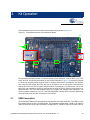
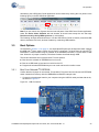
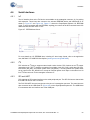
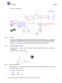
The SuperSpeed Explorer Kit includes the development board shown in Figure 3-1.
Figure 3-1. SuperSpeed Explorer Kit Development Board
J5
J2
USB 3.0
J3
USB 2.0
J4
The development board provides convenient access to FX3 interfaces, such as GPIF II, I2C, SPI,
UART, and I2S. The two 40-pin headers (on the reverse PCB side in Figure 3-1) provide FX3 signals
to connect to external boards using the GPIF II interface. Note that for convenience, the headers
have long pins that extend above the top side of the PCB for use as test points or attachment to
mating connectors. All GPIF II signals, which include a 32-bit data bus, 13 control lines, and a 100MHz clock, are available to connect to external devices such as FPGAs, CPLDs, image sensors, or
microcontrollers. The FX3 SDK examples help you program and evaluate these interfaces. The
GPIF II interface supports 32-, 24-, 16-, and 8-bit data/modes; unused GPIF II pins can alternatively
serve as GPIO pins if the GPIF II interface is not required.
3.1
USB Connectors
The SuperSpeed Explorer Kit development board provides two USB connectors. The USB 3.0 Type
B receptacle brings out the FX3 USB signals. This receptacle accepts either a USB 3.0 or USB 2.0
cable; the other end of the cable connects to a USB host PC. A USB 3.0 cable is included in the kit.
CYUSB3KIT-003 SuperSpeed Explorer Kit User Guide, Doc. # 001-93186 Rev. *A
20
Kit Operation
Use this port to test FX3 applications that communicate with a host PC at SuperSpeed or HighSpeed rates.
The USB 2.0 Micro-B receptacle connects to an onboard Cypress CY7C65215 USB-Serial Dual
Channel (UART/I2C/SPI) Bridge (www.cypress.com/go/CY7C65215), which is configured as an
integrated debugger operating at the USB Full-Speed rate. This chip provides a bridge between the
FX3 debug interface and a PC's USB port, enabling two debug methods: serial terminal messages
and JTAG debug. These debug methods are explained in Section 3.7 on page 33.
3.2
Jumpers
The SuperSpeed Explorer Kit development board contains four jumpers, labeled J2–J5. The jumper
settings are as follows.
Jumper J2: This jumper sets the voltage levels of the FX3 power domains VIO1, VIO2, and VIO3.
Inserting the jumper selects 3.3 V while removing the jumper selects 1.8 V. These domains set the
operating voltage of the FX3 interface pins. The default is to have the J2 jumper in place, selecting
the 3.3-V interface. This makes the interface compatible with the 3.3-V SRAM connected to the
GPIF II interface.
Jumper J3: This jumper is connected in series with the VBUS signal of the USB 3.0 connector. This
jumper must be inserted to power the development board. The J3 jumper is provided to measure the
development board's power consumption by removing the J3 jumper and connecting an ammeter
between the J3 pin headers.
Jumper J4: This jumper selects the FX3 boot method. Similar to all Cypress EZ-USB parts, the code
is loaded ("booted") into high-speed internal RAM for execution. The SuperSpeed Explorer Kit
supports USB boot and I2C boot. FX3 contains an internal ROM, where the boot code resides, and
an internal RAM, where application firmware and data are stored. At power-on, depending on this
jumper setting, FX3 boots from the internal ROM and then does one of the following:
■
If J4 is removed, then FX3 copies the application firmware from the onboard 2-Mbit I2C EEPROM
to FX3's internal RAM and then enumerates with the functionality defined in the application firmware. If there is no valid firmware in EEPROM or if the EEPROM is disabled or not present, then
FX3 enumerates as a bootloader device and enables firmware download to internal RAM through
USB. This method of booting is referred to as I2C boot, with fallback to USB. The USBBulkSourceSinkLED firmware is stored in the onboard EEPROM when the SuperSpeed Explorer Kit
development board leaves the Cypress factory. The steps to store new firmware in EEPROM and
then boot from it are explained in Section 3.5.3 on page 28.
■
If J4 is inserted, then FX3 enumerates as a bootloader device and allows the application firmware
to be loaded to internal RAM through USB. This boot method is referred to as USB boot. In this
boot method, you can download the application firmware to FX3's RAM using a host application.
The steps to load firmware to FX3's RAM using this boot method are explained in a later section.
The J4 jumper is labeled "PMODE" to correspond to the FX3 PMODE0 pin.
Jumper J5: This jumper is connected in series with the CTL0 pin of the FX3. The CTL0 pin is used
as a chip select signal for the onboard SRAM external to FX3. J5 must be inserted for applications
that use the SRAM. It is recommended that you deselect the SRAM by removing J5 when the SRAM
is not used. Note that the SRAM operates at 3.3 V and does not support 1.8-V signaling. Therefore,
the SRAM must be deselected if the 1.8-V interface is selected (if J2 is removed, then J5 should also
be removed). Table 3-1 summarizes the default jumper settings.
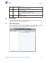
Table 3-1. Default Jumper Settings
Jumper
Jumper State
Function
CYUSB3KIT-003 SuperSpeed Explorer Kit User Guide, Doc. # 001-93186 Rev. *A
21
Kit Operation
Table 3-1. Default Jumper Settings
3.3
J2
Short
Power domain VIO1, VIO2, and VOI3 voltages set to 3.3 V to support external
3.3-V interfaces and the onboard SRAM.
J3
Short
Development board is powered from USB 3.0 VBUS. This jumper must be in
place for normal operation.
J4
Open
J5
Open
Boot from I2C EEPROM on the development board, if a valid firmware image is
present in EEPROM; otherwise, fall back to USB boot.
Note By default, USBBulkSourceSink with LED Blink firmware is stored by
EEPROM.
Deselect external SRAM.
Power Mode
The development board operates only in USB bus-powered mode. Note that an FX3 design can also
be self-powered but this feature is not supported in this kit.
3.4
USB Control Center
To explore various FX3 boot options, open Cypress’s USB Control Center application by choosing
Start menu All Programs > Cypress > Cypress USBSuite > Control Center (see Figure 3-2).
Figure 3-2. USB Control Center Opening Screen
CYUSB3KIT-003 SuperSpeed Explorer Kit User Guide, Doc. # 001-93186 Rev. *A
22
Kit Operation
Alternatively, the USB Control Center application can be launched by clicking the icon (shown in the
following figure) in the EZ USB Suite application.
Note If you see various non-Cypress devices in the left panel of the USB Control Center application,
select the Device Class Selection tab and deselect all check boxes except the one that says
Devices served by the CyUSB3.sys driver (or a derivative).
The following sections demonstrate how to use the USB Control Center to identify connected USB
devices, download FX3 code, and test firmware by conducting USB transfers.
3.5
Boot Options
As described in Section 3.2 on page 21, the SuperSpeed Explorer Kit development board supports
the USB and I2C boot options, When the J4 jumper is removed, FX3 boots from the onboard I2C
EEPROM if a valid firmware image is available in the EEPROM; otherwise, FX3 falls back to USB
boot. When the J4 jumper is inserted, FX3 allows firmware download through USB.
This section discusses how to execute three FX3 boot options:
3.5.1
■
Boot from the onboard I2C EEPROM and run its code.
■
Boot as a USB loader to load and run code from the PC.
■
Program the onboard EEPROM with your own code and boot from it after a reset.
Boot From Onboard I2C EEPROM
Confirm that the J4 jumper is not inserted. This enables FX3 to boot from the onboard I2C EEPROM,
which is loaded in the factory with the USBBulkSourceSinkLED example code.
1. Connect the development board to your computer using the USB 3.0 cable provided with the kit,
as shown in Figure 3-3.
Figure 3-3. USB Connection
LED2
CYUSB3KIT-003 SuperSpeed Explorer Kit User Guide, Doc. # 001-93186 Rev. *A
23
Kit Operation
2. After connecting the development board to the host, wait for the Windows drivers to install. If the
drivers do not install automatically, follow the steps in the “Appendix” on page 52 to manually
install the drivers.
3. After the driver installation is complete, observe the blue LED (LED2). If the development board
is connected to a USB 3.0 port, the blue LED (LED2) blinks. If the development board is
connected to a USB 2.0 port, the blue LED (LED2) stays ON. If the development board is
connected to a USB 1.1 port, the blue LED (LED2) stays OFF.
Note This is a useful way to speed-test USB ports on a PC, where the USB operating speed is
not always obvious. For example, some desktop PCs have the telltale blue plastic inserts (which
are supposed to indicate USB 3.0) in both front and rear USB receptacles. Nevertheless, the
front-panel receptacles often operate only at a USB 2.0 rate (480 Mbps).
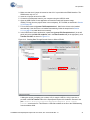
4. Take a look at the USB Control Center. It should appear as shown in Figure 3-4. The USB
Control Center detects the development board, which is named Cypress FX3 USB
StreamerExample Device. This appears as the heading in a device tree in the left panel.
Figure 3-4. FX3 Board Connected to a USB 2.0 Port
With the Descriptor Info tab selected, expand the device tree nodes and click on the various
components – Device, Configuration, Interface, and so on. Notice that the descriptor information
changes according to what is highlighted in the device tree. This illustrates the context-sensitive
nature of the USB Control Center – you should select an item in the device tree before conducting a
particular USB operation.
CYUSB3KIT-003 SuperSpeed Explorer Kit User Guide, Doc. # 001-93186 Rev. *A
24
Kit Operation
In Figure 3-4, the development board is connected to a USB 2.0 receptacle. One way to determine
this is to look at the BcdUSB entry "02 10", which indicates the USB specification version under
which the device enumerated (USB 2.1). With this connection, the blue LED (LED2) on the board
stays ON to indicate the USB 2.0 High-Speed connection.
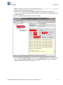
Compare Figure 3-4 with Figure 3-5, where the same development board was unplugged from the
front-panel USB 2.0 receptacle and plugged into a rear-panel USB 3.0 receptacle on the same PC.
The blue LED now blinks and the BcdUSB Descriptor Info entry now reads "03 00", indicating a
USB 3.0 device. SuperSpeed devices also uniquely contain Binary Device Object Store (BOS)
descriptors, as shown in Figure 3-5.
The same development board is now operating with SuperSpeed capability. This demonstrates an
important USB 3.0/FX3 feature: Firmware can be written to automatically detect and support
SuperSpeed or legacy USB attachments. The example Cypress code shows how this can be done.
Figure 3-5. Same Device, Different Port, Now Operating as a USB 3.0 Device
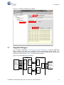
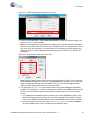
Another USB Control Center option is to conduct USB transfers to and from the FX3 board. The
example firmware booted from the EEPROM contains code to respond to a custom USB request
type called a ‘vendor request’. To exercise this option, select the Control endpoint (0x00) item in
the device tree and click the Data Transfers tab, as shown in Figure 3-6. Then select ‘Vendor’ from
the Req type (USB request type) drop-down list. The example firmware responds to a vendor
request code of 0xAA, which you enter in the Req code box. Your panel values should look similar to
those in Figure 3-6. Enter a number between 0 and 9 in the Data to send (Hex) box and click the
CYUSB3KIT-003 SuperSpeed Explorer Kit User Guide, Doc. # 001-93186 Rev. *A
25
Kit Operation
Transfer Data button. The LED blinks with a 1-second period and the ON time corresponding to the
data you enter times 100 milliseconds. Entries greater than nine (LED ON for 900 ms) blink at a fixed
500-ms ON time.
Note Make sure there are no spaces before the number you type into the Data to send (Hex) text
box.
Figure 3-6. Using the USB Control Center to Set the FX3 LED Blink Rate
3.5.2
Boot as a USB Loader
To demonstrate the FX3 operation as a USB bootloader, follow these instructions:
1. Unplug the development board, insert the J4 jumper, and reattach the development board to the
PC. In USB boot mode, FX3 enumerates as a high-speed bootloader using Vendor ID VID=04B4
and Product ID PID=0x00F3. FX3 identifies itself in the USB Control Center as the Cypress FX3
Bootloader Device, as shown in Figure 3-7. It may take several seconds for this device entry to
appear.
CYUSB3KIT-003 SuperSpeed Explorer Kit User Guide, Doc. # 001-93186 Rev. *A
26
Kit Operation
Figure 3-7. FX3 as a USB Bootloader
Note The FX3 bootloader operates at high speed (USB 2.0) even if connected to a USB 3.0 port.
Therefore, it appears as a USB 2.0 device, seen by BcdSUB = "02 00" and no BOS
(SuperSpeed) descriptor.
2. When the FX3 enumerates as a bootloader device, it can be used to download code into internal
RAM or to program the onboard EEPROM with custom code. To download and execute code
from the FX3 internal RAM, choose Program > FX3 > RAM, as shown in Figure 3-8.
Figure 3-8. Programming FX3 RAM
3. A pop-up window asks for a file to download. Navigate to the same example firmware application
available in the path (this is the same firmware stored in the EEPROM when the SuperSpeed
Explorer Kit development board leaves the Cypress factory) at:
<Install Directory>\Cypress\SuperSpeed Explorer Kit\1.0\Firmware\USBBulk
SourceSinkLED\Debug
Note For Windows 7 and above, the default install directory is C:\Program Files (x86). For
Windows XP, the default install directory is C:\Program Files.
CYUSB3KIT-003 SuperSpeed Explorer Kit User Guide, Doc. # 001-93186 Rev. *A
27
Kit Operation
Notice that after loading the firmware from the PC, the FX3 automatically disconnects from USB and
immediately reappears in the USB Control Center as the device created by the code it loaded,
namely, the Cypress FX3 USB StreamerExample Device, as described previously. You can confirm
operation of the code using the same steps as those used to change the blink rate. The only
difference is that this code is loaded into the FX3 RAM from the PC instead of the EEPROM.
This method can be used to download and test any code you develop using the FX3 SDK. Because
loading into RAM is extremely fast, the load-and-test cycles can be very short.
3.5.3
Program the EEPROM
You may want to have the FX3 boot from the onboard EEPROM using the code you put into it.
1. To program your own code into the EEPROM and boot directly to it at power-on, start the FX3
bootloader by inserting the J4 jumper and then connecting the development board to the PC.
Note that pressing the RESET button has the same effect as disconnecting-then-reconnecting to
the USB. As long as the J4 jumper is in place, pressing the RESET button always brings the
SuperSpeed Explorer Kit development board back as a code loader. This allows you to load new
code builds during development without disconnecting the USB cable. This time, select I2C
EEPROM as the target device instead of RAM in the USB Control Center application (Figure 3.6).
This causes FX3 to invoke a secondary loader called Cypress FX3 USB BootProgrammer Device
(Figure 3.6), as opposed to the "BootLoader" device used to program the FX3 RAM in the
previous section.
Note The BootProgrammer has different VID/PID values than the BootLoader, which may trigger
driver installation the first time it is used. If the driver does not install automatically, follow the
steps in Section A.1.1 on page 52 to manually install the driver.
Figure 3-9. I2C EEPROM Download Option
Figure 3-10. FX3 Re-Enumerates as a Cypress FX3 USB BootProgrammer Device
2. After selecting I2C EEPROM as the programming target, navigate to the .img file to be loaded
and click Open. After the BootProgrammer code erases and reprograms the EEPROM, a
success message appears in the lower left corner of the USB Control Center. Note that erasing
and programming EEPROM takes much longer than programming internal RAM, on the order of
20-30 seconds.
CYUSB3KIT-003 SuperSpeed Explorer Kit User Guide, Doc. # 001-93186 Rev. *A
28
Kit Operation
3. Disconnect the USB cable, remove the J4 jumper, reattach the cable, and the FX3 boots with the
code from EEPROM.
3.6
Firmware Examples
Two firmware examples are provided with the SuperSpeed Explorer Kit installation in addition to
those provided with the SDK. The SDK examples are available in the Firmware folder of the FX3
SDK. To import an SDK example, refer to the steps in Section 2.6.2 on page 16. For Windows 7 and
above, the default location of the firmware folder is C:\Program Files (x86)\Cypress\EZUSB FX3 SDK\1.3\firmware. For Windows XP, the default install directory is C:\Program
Files\Cypress\EZ-USB FX3 SDK\1.3\firmware.
Note The SuperSpeed Explorer Kit development board does not support FX3 USB HS-OTG
functionality. Therefore, the OTG/host-based example firmware projects provided with the FX3 SDK
do not apply to this kit. In addition, SDK example firmware projects that are meant for FX3S and CX3
are not applicable to this development board.
3.6.1
USBBulkSourceSink with LED Blink
This is the default firmware stored in the kit's onboard EEPROM. As described in the previous
section, this firmware supports the following features:
■
It implements endless data sources and sinks over a pair of USB bulk endpoints.
■
The blue LED (LED2) blinks at connection, depending on the USB host controller capability. If the
development board is connected to a USB 3.0 port, the blue LED (LED2) blinks and if it is connected to a USB 2.0 port, the blue LED (LED2) stays ON. If the development board is connected
to a USB 1.1 port, the blue LED (LED2) stays OFF.
■
The LED blink rate can be modified through a vendor command.
The firmware source (USBBulkSourceSinkLED) is located in the Firmware folder of the SuperSpeed
Explorer Kit installation. To study and modify this example, import this project into the EZ USB Suite
and build the firmware image (see Section 2.6 on page 15). The firmware will be copied to the
EZ USB Suite Workspace folder and a newly built firmware image will be available in the same path
after building the project.
In Section 3.5.1 on page 23, the Cypress USB Control Center was used to exercise the LED
functionality of this example. A second Windows application, streamer.exe, can be used to exercise
the data source and sink capabilities. This application is available at:
<Install Directory>\Cypress\EZ-USB FX3SDK\1.3\application\cpp\streamer\x86\Release
Note For Windows 7 and above, the default install directory is C:\Program Files (x86). For
Windows XP, the default install directory is C:\Program Files.
Before running streamer.exe, make sure the Cypress FX3 USB StreamerExample Device is loaded
into FX3, as detailed in Section 3.5.1 on page 23.
As Figure 3-11 shows, select 256 as Packets per Xfer and 64 as Xfers to Queue from the dropdown list available in the Streamer application.
■
Packets per Xfer: A transfer is a collection of packets for one data set. A greater number of packets for each transfer reduces the USB overhead and achieves higher data throughput.
■
Xfers to Queue: This setting initiates multiple transfers and adds them to a task queue, which
reduces the latency between successive transfers on the host application side. Therefore, queuing more transfers results in a higher data rate.
CYUSB3KIT-003 SuperSpeed Explorer Kit User Guide, Doc. # 001-93186 Rev. *A
29
Kit Operation
Figure 3-11. Streamer.exe
The SuperSpeed bulk throughput depends on the burst size, buffer size, and the number of buffers.
This firmware is already optimized to achieve maximum throughput. Refer to AN86947 - Optimizing
USB 3.0 Throughput with EZ-USB® FX3™ (www.cypress.com/go/AN86947) for more details about
the parameters that affect the throughput in the bulk source/sink firmware.
AN86947 (www.cypress.com/go/AN86947) lists the USB 3.0 throughput numbers using internally
provided FX3 data. The USB 3.0 throughput numbers will be slightly lower when the data originates
from an external device into FX3 through GPIF II. Refer to AN65974 - Designing with the EZ-USB®
FX3™ Slave FIFO Interface (www.cypress.com/go/AN65974) for the throughput numbers when an
FPGA supplies data to FX3 via the GPIF II interface.
3.6.2
SRAM Example
This firmware supports reading and writing to the onboard SRAM. The LED blinking activity is
maintained in this firmware as well. You can find the firmware source (SRAM_FX3) in the Firmware
folder of the SuperSpeed Explorer Kit installation. Be sure to import this project into the EZ USB
Suite and build the firmware image, if not already done. The firmware will be copied to the EZ USB
Suite Workspace folder, and a newly built firmware image will be available in the same path.
To test the functionality of this firmware, follow these steps.
1. Disconnect the development board from the computer if it is already connected.
2. Insert the J5 jumper to enable SRAM.
CYUSB3KIT-003 SuperSpeed Explorer Kit User Guide, Doc. # 001-93186 Rev. *A
30
Kit Operation
3. Make sure that the J2 jumper is inserted so that 3.3 V is provided to the SRAM interface. The
SRAM works only at 3.3 V.
4. Insert the J4 jumper to boot from USB.
5. Connect the development board to your computer using the USB 3.0 cable.
6. Open the USB Control Center application and load the newly built firmware image,
SRAM_FX3.img (from the project folder in the workspace), to FX3 RAM, as described in Section
3.5.2 on page 26.
7. FX3 re-enumerates as Cypress FX3 Example device 1. Wait for the drivers to be installed
automatically. If the drivers are not installed automatically, follow the steps listed in Section
A.1.1 on page 52 to install the drivers manually.
8. In the USB Control Center application, expand the Cypress FX3 Example device 1 (in the left
panel) and select the Bulk out endpoint; and in the Data Transfers tab (in the right panel), click
Transfer File-OUT, as shown in Figure 3-12.
Figure 3-12. Sending Data Through Control Center to Write to SRAM
A dialog box opens, prompting you to select a file. A sample 1-KB file, 1024_Count.hex, is
provided in the File Transfer folder of the SuperSpeed Explorer Kit installation. Browse to the
path <Install Directory>\Cypress\SuperSpeed Explorer Kit\1.0\File
Transfer to select the file. This writes the 1-KB data available in the file to the SRAM starting
from the address 0x00.
CYUSB3KIT-003 SuperSpeed Explorer Kit User Guide, Doc. # 001-93186 Rev. *A
31
Kit Operation
Note For Windows 7 and above, the default install directory is C:\Program Files (x86). For
Windows XP, the default install directory is C:\Program Files.
9. Send a vendor command with the Req code 0xBB to the control endpoint, as shown in
Figure 3-13. This step is necessary to switch the GPIF state machine from the SRAM Write cycle
to SRAM read cycle.
Figure 3-13. Sending Vendor Request to Read From SRAM
10.Select the Bulk in endpoint(0x81) in the left panel. In the Data Transfers tab (in the right panel),
enter ‘1024’ in the Bytes to transfer field and click Transfer Data-IN to read the 1024 bytes
written to SRAM in the previous step. (See Figure 3-14).
CYUSB3KIT-003 SuperSpeed Explorer Kit User Guide, Doc. # 001-93186 Rev. *A
32
Kit Operation
Figure 3-14. Reading 1024 Bytes From SRAM
3.7
Integrated Debugger
The CY7C65215 USB-Serial IC (www.cypress.com/go/CY7C65215) is a full-speed USB-Serial
bridge controller that offers two configurable serial communications blocks (SCBs). The
development board uses the first serial channel of the CY7C65215 as a UART and the second serial
channel as a JTAG interface. Figure 3-15 shows the block diagram.
Figure 3-15. Block Diagram of CY7C65215
EZ-USB FX3
USB-Serial IC (CY7C65215)
SS Tx+
SS Tx-
USB 3.0
SS Rx-
Type B
SS Rx+
Connector
(J1)
DM
DP
UART
UART
SCB0
USB
DM
Micro B
DP
USB 2.0
VBUS
Connecto
USB
3.0
2.0
VBUS
GND
GND
r (J8)
JTAG
JTAG
SCB1
CYUSB3KIT-003 SuperSpeed Explorer Kit User Guide, Doc. # 001-93186 Rev. *A
33
Kit Operation
3.7.1
UART
To use the UART functionality on the SuperSpeed Explorer Kit, follow these instructions:
1. Use J1 to connect the development board to your computer. This powers the board and provides
the USB 3.0 conduit to FX3. Then, use a micro USB 2.0 cable to connect J8 to your computer.
This connection makes the integrated debugger enumerate with three interfaces. One of the
interfaces will be COM port. You can verify the entry in the Device Manager (Figure 3-16).
Figure 3-16. USB Serial IC Enumerating as COM Port
You can use any standard UART communication terminal, such as Tera Term, to display the messages transmitted over the UART.
Note Some PC terminal applications put an upper limit on COM port choices, for example offering support only up to COM7. If your USB serial port has a COM number that is too high for your
PC terminal app, see Section A.2 on page 54, for a method to remove inactive COM port assignments to free up the lower-numbered COM ports.
2. When the COM port entry is verified in the Windows Device Manager, open Tera Term (or any
other standard UART communication terminal), select the USB Serial Port (COM#), and click OK,
as shown in Figure 3-18.
Note The Tera Term application is known to have problems of data loss at very low baud rates
(1200 and below) with the integrated debugger, when larger blocks of data are received or transmitted over UART. You can use other standard COM port terminals, such as HyperTerminal or
TestView, if you encounter such data loss issue with the Tera Term application.
CYUSB3KIT-003 SuperSpeed Explorer Kit User Guide, Doc. # 001-93186 Rev. *A
34
Kit Operation
Figure 3-17. Selecting USB-Serial COM Port in Tera Term
3. In the Tera Term application, choose Setup > Serial Port to change the COM port settings, as
shown in Figure 3-18 and click OK.
Note In all the SDK firmware projects and the firmware projects provided with the SuperSpeed
Explorer Kit, the UART block of the FX3 device is initialized to work at 115200 baud rate. Therefore, in the Tera Term application, you should select the 115200 baud rate while setting up the
COM port, unless you have changed the baud rate setting for the UART block in the FX3 firmware project.
Figure 3-18. Setting Up the COM Port in Tera Term
Note Though the UART hardware flow control is supported by the FX3 SDK, it is not supported
by the SuperSpeed Explorer Kit. Therefore, the Flow Control field should be set to “none” in the
UART communication terminal. When the UART interface is used while debugging through
JTAG, the UART baud rate should not be more than 115200.
4. The debug prints in Figure 3-19 can be observed when running the USBBulkSourceSinkLED
firmware on the FX3 device. To obtain the debug prints available in the USBBulkSourceSinkLED
project over UART, follow the steps mentioned above and then perform one of the following
actions:
a. The USBBulkSourceSinkLED firmware is stored in the onboard EEPROM by default. If the
EEPROM still has the same firmware, then remove the J4 jumper and press the FX3 reset
button so the USBBulkSourceSinkLED firmware from EEPROM is loaded to the FX3 RAM.
b. Insert the J4 jumper and follow the steps in Section 3.5.2 on page 26 to load the USBBulkSourceSinkLED firmware to the FX3 RAM using the USB boot option.
CYUSB3KIT-003 SuperSpeed Explorer Kit User Guide, Doc. # 001-93186 Rev. *A
35
Kit Operation
Figure 3-19. UART Debug Prints When Running USBBulkSourceSinkLED Firmware Project
3.7.2
JTAG
The JTAG interface provided by the integrated debugger supports the OpenJTAG protocol and uses
the OpenOCD demon tool on the host to conduct a debugging session. All the required files for
JTAG debugging are provided with the SuperSpeed Explorer Kit installation and are available in the
following default path after installation: <Install Directory>\Cypress\SuperSpeed Explorer
Kit\1.0\USBSerialOpenOCD.
Note For Windows 7 and above, the default install directory is C:\Program Files (x86). For
Windows XP, the default install directory is C:\Program Files.
The OpenOCD demon tool is tailored to work with the integrated debugger. The OpenOCD
executable provided with the SuperSpeed Explorer Kit setup is generated by patching OpenOCD
0.7.0 (http://openocd.sourceforge.net/) and then compiling to make it work with the integrated
debugger provided on the development board. The configuration file, arm926ejs_FX3.cfg, is also
provided as required by OpenOCD to identify the USB-Serial IC as a JTAG debugger and FX3 as a
target.
Follow these steps to debug the FX3 firmware using the onboard USB-Serial IC as a JTAG
debugger.
Hardware Setup
1. Insert the J4 jumper and connect the development board (USB 3.0 connector J1) to your
computer using the USB 3.0 cable.
2. Connect the development board to your computer using a micro USB cable through the USB 2.0
microconnector J8. Here, the USB-Serial IC (CY7C65215) acts as a USB-JTAG device.
3. Wait for the USB-Serial IC to enumerate and install the Cypress driver automatically. If the driver
does not install automatically, follow the steps in Section A.1.1 on page 52 to manually install the
driver.
After driver installation, the USB-Serial interfaces can be identified as:
■
USB Serial Port (COMx): This interface acts as an UART interface.
■
USB-Serial (Dual Channel) Vendor MFG: This interface is used to configure the USB-Serial IC.
■
USB-Serial (Dual Channel) Vendor 1: This interface acts as a JTAG interface.
Software Setup:
1. Open the EZ USB Suite, and highlight the USBBulkSourceSinkLED project you loaded and
compiled in Section 3.6.1 on page 29.
2. Create an external tool configuration for the debugger. In the EZ USB Suite, choose Run >
External Tools > External Tools Configurations. Double-click Program. A new run
configuration opens. Give the configuration a name, and fill in the fields as follows and as shown
in Figure 3-20.
CYUSB3KIT-003 SuperSpeed Explorer Kit User Guide, Doc. # 001-93186 Rev. *A
36
Kit Operation
Figure 3-20. External Tool Configuration in EZ USB Suite
Location:
This field specifies the location for the OpenOCD executable (openOCD.exe), available in the
USBSerialOpenOCD folder of the SuperSpeed Explorer Kit installation. For a SuperSpeed Explorer
Kit installation using the default installation path, copy and paste the following path in this field:
C:\Program Files (x86)\Cypress\SuperSpeed Explorer
Kit\1.0\USBSerialOpenOCD\openOCD.exe
Working Directory:
This field specifies the OpenOCD working directory. Use the same directory that contains the
executable. For a SuperSpeed Explorer Kit installation using the default installation path, copy and
paste the following path in this field:
C:\Program Files (x86)\Cypress\SuperSpeed Explorer Kit\1.0\USBSerialOpenOCD\
Arguments:
This field specifies the arguments supplied to the OpenOCD executable. The file,
arm926ejs_FX3.cfg, provided in the USBSerialOpenOCD folder of the SuperSpeed Explorer Kit
installation contains the JTAG debugger and the target (FX3) details as required by OpenOCD. Copy
and paste the following argument:
-f arm926ejs_FX3.cfg
Note When you click Run, the EZ USB Suite will build the entire workspace before launching the
External Tool configuration. To eliminate this step, you can uncheck the Build before launch option
in the Build tab.
CYUSB3KIT-003 SuperSpeed Explorer Kit User Guide, Doc. # 001-93186 Rev. *A
37
Kit Operation
When you click Run, OpenOCD is invoked and the messages shown in Figure 3-21 appear in the
EZ USB Suite Console window, indicating that OpenOCD has accepted the integrated debugger as
a JTAG adapter, has recognized FX3 as a target device, and is now running in the background as a
debug server.
Note You need to create the external tool configuration only once for each JTAG debugger per
Workspace. The configuration you just entered is saved in the EZ USB Suite.
Figure 3-21. Console Window in EZ USB Suite
Follow these steps to create a debug configuration for the project. Because individual projects
require individual debug configurations, this procedure must be done once for every project. To
create a debug configuration for a project, make sure to import the firmware project into the
workspace and build the project, if not already done. Then, follow these steps:
1. Select the desired project in the Project Explorer; then, go to Run > Debug Configurations, as
shown in Figure 3-22.
CYUSB3KIT-003 SuperSpeed Explorer Kit User Guide, Doc. # 001-93186 Rev. *A
38
Kit Operation
Figure 3-22. Generating Debug Configuration in EZ USB Suite
2. Double-click Zylin Embedded debug (Native). A new debug configuration opens with the
firmware name as the Project name. Confirm that EZ USB Suite has filled in the fields as shown
in Figure 3-23. If the C/C++ Application field is empty, click Search Project and select the
Debug or Release build of the .elf file, which was built previously.
Figure 3-23. Debug Configuration in EZ USB Suite
Double-click
CYUSB3KIT-003 SuperSpeed Explorer Kit User Guide, Doc. # 001-93186 Rev. *A
39
Kit Operation
3. In the Debugger tab, browse to the path shown in Figure 3-24 for the GDB debugger. Leave the
GDB command file field blank.
Figure 3-24. Debugger Tab of Debug Configurations Window in EZ USB Suite
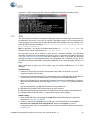
4. In the Commands tab (Figure 3-25), copy and paste the following text into the 'Initialize'
commands section:
set prompt (arm-gdb)
# This connects to a target via netsiliconLibRemote
# listening for commands on this PC's tcp port 3333
target remote localhost:3333
monitor reset halt
# Set the processor to SVC mode monitor reg cpsr 0xd3
# Disable all interrupts
monitor mww 0xFFFFF014 0xFFFFFFFF
# Enable the TCMs
monitor mww 0x40000000 0xE3A00015
monitor mww 0x40000004 0xEE090F31
monitor mww 0x40000008 0xE240024F
monitor mww 0x4000000C 0xEE090F11
# Set the PC to 0x40000000
monitor reg pc 0x40000000
si
si
si
si
In the 'Run' commands section, enter:
load
The 'Initialize' and 'Run' commands are the GDB commands to initialize and run the JTAG target
device, in this case, FX3.
CYUSB3KIT-003 SuperSpeed Explorer Kit User Guide, Doc. # 001-93186 Rev. *A
40
Kit Operation
Figure 3-25. Commands Tab of Debug Configurations Window in EZ USB Suite
5. Click Debug. Accept the option to switch to the "Debug Perspective". An Eclipse perspective is a
screen layout optimized for various activities. In the upper right corner of the Eclipse screen, you
can select Debug for debugging or C/C++ for code development. The executable firmware
launches, and the debug perspective (view) opens, as shown in Figure 3-26.
Figure 3-26. Launching Debug Session
CYUSB3KIT-003 SuperSpeed Explorer Kit User Guide, Doc. # 001-93186 Rev. *A
41
Kit Operation
The firmware launch status is shown in the bottom right corner of the EZ USB Suite debug perspective. After the firmware is launched completely, a second window opens with the message
No source available for "", as shown in Figure 3-27.
Figure 3-27. Launching Debug Session Complete
6. Ignore this message and click Resume. The debug point stops at "main" as shown in
Figure 3-28.
Figure 3-28. Debugger Stops at Main
CYUSB3KIT-003 SuperSpeed Explorer Kit User Guide, Doc. # 001-93186 Rev. *A
42
Kit Operation
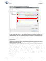
7. Apply breakpoints wherever necessary and click Resume. For example, apply breakpoints in the
function BulkSrcSinkAppThread_Entry, as shown in Figure 3-29. To apply a breakpoint, doubleclick on the blue bar to the left of the line. This part of the firmware toggles the GPIO to which the
blue LED (LED2) is connected.
Note Do not add breakpoints in the sections of code where USB requests are handled (CyFxBulkSrcSinkApplnUSBSetupCB, CyFxBulkSrcSinkApplnUSBEventCB functions in the USBBulkSourceSinkLED firmware project), because they affect the USB enumeration process or any
other control request handling. Similarly, avoid placing breakpoints in the GPIF callback or DMA
callback sections of the firmware project, as these functions are called inside the FX3 SDK libraries. Applying a breakpoint inside these functions may affect how the firmware works in applications where FX3 is receiving continuous data over GPIF II and is streaming that data to the host.
Figure 3-29. Applying Breakpoints in the Firmware
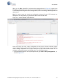
8. After the debugger stops at "main", click Resume. The debugger stops at the first breakpoint, as
shown in Figure 3-30. This line of the firmware switches the blue LED (LED2) ON. The second
breakpoint is applied at the line of firmware that switches the blue LED (LED2) OFF.
CYUSB3KIT-003 SuperSpeed Explorer Kit User Guide, Doc. # 001-93186 Rev. *A
43
Kit Operation
Figure 3-30. Debugger Stops at First Breakpoint
9. Click the Step Over icon until you reach the second breakpoint. Note that if the development
board is connected to the SuperSpeed host, the debugger will reach the second breakpoint. If the
development board is connected to the high-speed host, the debugger will not reach the second
breakpoint, because the initial state of the blue LED (LED2) is that it will stay on. This part of the
code is in an infinite loop and clicking Resume will make the debugger stop at the first and
second breakpoints one after the other. Use the Step Into or Step Over icons when required.
Note All FX3 SDK APIs should be "stepped over". "Stepping into" FX3 SDK APIs (APIs are the
function calls that start with "CyU3P" in the firmware) will result in a warning message of "source
not available at…". If you encounter this message, click the Step Return icon.
10.To stop the debug session, click the Terminate icon (see Figure 3-28). When the debug session
is terminated, it can be launched again with the Debug Configurations icon shown in Figure 3-31.
Be sure to reset FX3 before loading the debug configuration again. Clicking the drop-down arrow
of the Debug Configurations icon will display all the debug configurations available. You can
select the desired debug configuration from the drop-down list.
Figure 3-31. Debug Configurations Icon
11. To completely stop the debug session, drop the GDB connection, and terminate the OpenOCD
tool (running in the background), click the Drop GDB Session icon twice, instead of clicking the
CYUSB3KIT-003 SuperSpeed Explorer Kit User Guide, Doc. # 001-93186 Rev. *A
44
Kit Operation
Terminate icon as explained in the previous step. Clicking the Drop GDP Session icon the first
time stops the GDB session, and then clicking it again terminates the OpenOCD application.
Note It is recommended that you drop the GDB session and terminate the OpenOCD application
before unplugging the USB cable of the integrated debugger, because the OpenOCD tool keeps
polling for the availability of the integrated debugger. If the integrated debugger is unplugged
without dropping the GDB session, continuous "CyJTAGRead failed" and "CyJTAGWrite failed"
messages will be flashed in the Console window of the EZ USB Suite. Terminating the OpenOCD
application will stop this activity.
If the GDB session is dropped and the OpenOCD application is terminated, then you should run
the external tool configuration before starting the debug session again. Figure 3-32 shows the
icon for External Tools Configurations. The drop-down list associated with this icon identifies
all the external tools configurations saved with the EZ USB Suite. When the external tool configuration is run, you can launch the debug session to debug the firmware.
Figure 3-32. External Tools Configurations Icon
The Debug perspective (view) is the best one to use for debug sessions. To return to the code
development perspective, click the Open Perspective icon and select C/C++, as shown in
Figure 3-33.
Figure 3-33. Icon to Switch to C/C++ Perspective
CYUSB3KIT-003 SuperSpeed Explorer Kit User Guide, Doc. # 001-93186 Rev. *A
45
4.
Hardware
This chapter describes the hardware interfaces and circuits available on the SuperSpeed Explorer
Kit development board. It covers the following topics:
4.1
■
Power supply
■
USB 3.0 receptacle connector
■
FX3 clocking mechanism using onboard crystal
■
User push button
■
User LED
■
GPIF II connector
■
Reset circuit
■
Serial interfaces: I2S, I2C, SPI, UART, and JTAG
Power Supply
The SuperSpeed Explorer Kit development board is powered from the USB 3.0 connector J1. This
development board does not support self-powered mode, although the FX3 device does support it.
Select voltage levels for FX3 I/O power domains through the J2 jumper, as shown in Table 4-1.
Table 4-1. Power Supply Domain
Power Domains
Jumper
Position
Voltage Level
VIO1, VIO2, VIO3
J2
Short (default)
3.3 V
VIO1, VIO2, VIO3
J2
Open
1.8 V
FX3 I/O voltage domains VIO4 and VIO5 are fixed to 3.3 V. If you are using the onboard SRAM, you
must select the 3.3 V option.
The FX3 device has additional power domains (U3TXVDDQ, U3RXVDDQ, AVDD, and VDD), which
are fixed at 1.2 V on the development board.
Refer to the "Pin Description" section of the EZ-USB FX3: SuperSpeed USB Controller datasheet
(www.cypress.com/go/CYUSB301X) for details on configuring the I/O in each power domain.
Figure 4-1 shows the circuit used to switch the voltage level using the J2 jumper.
CYUSB3KIT-003 SuperSpeed Explorer Kit User Guide, Doc. # 001-93186 Rev. *A
46
Hardware
Figure 4-1. Circuit to Switch Voltage Level for FX3 VIO Domain
4.2
USB 3.0 Receptacle Connector
A standard B-type USB 3.0 connector is on the development board. Figure 4-2 shows the USB 3.0
pins (SS_TX_M, SS_TX_P, SS_RX_P, and SS_RX_M) and USB 2.0 pins (D+ and D–) that are
available on the J1 USB connector. The USB 3.0 and USB 2.0 lines go through an ESD protection
device. This connector accepts either the newer USB 3.0 plug or an older USB 1.1/2.0 plug.
Figure 4-2. USB 3.0 Type B Connector and ESD Device
4.3
FX3 Clock
On the development board, the clock for the FX3 is provided by an onboard 19.2-MHz crystal
connected to the FX3 XTALIN and XTALOUT pins, as shown in Figure 4-3. The FSLC[0:2] lines of
FX3 are tied to ground to select the 19.2-MHz crystal for clocking, as shown in Figure 4-4.
CYUSB3KIT-003 SuperSpeed Explorer Kit User Guide, Doc. # 001-93186 Rev. *A
47
Hardware
Figure 4-3. Crystal Circuit
Figure 4-4. FSLC[0:2] Lines Pulled to Ground
4.4
GPIF II Connector
The General Programmable Interface, Gen 2 (GPIF II) enables functionality similar to, but more
advanced than that of the FX2LP™ GPIF. It is a programmable state machine that enables a flexible
interface, functioning either as a master or a slave using industry-standard or proprietary interfaces.
You can implement both parallel and serial interfaces with GPIF II. The development board provides
two rectangular connectors to interface with external processors, ASICs, DSPs, or FPGAs, as
Figure 4-5 shows.
If the GPIF II is not used as the FX3 firmware, these pins become the FX3 GPIO pins.
Figure 4-5. GPIF II Lines on Rectangular Connectors
CYUSB3KIT-003 SuperSpeed Explorer Kit User Guide, Doc. # 001-93186 Rev. *A
48
Hardware
4.4.1
SuperSpeed Explorer Kit Interconnect Boards
Two popular applications of FX3 are the following:
■
Use FX3 as a USB controller for an image sensor to stream uncompressed data
■
Implement the synchronous slave FIFO configuration of FX3 to interface to an FPGA
The application note, AN75779 - How to Implement an Image Sensor Interface with EZ-USB®
FX3™ in a USB Video Class (UVC) Framework (www.cypress.com/go/AN75779) explains how to
implement an image sensor interface with FX3 in a USB video class (UVC) framework. The project
provided with this application note interfaces FX3 with an Aptina MT9M114 Image Sensor
(www.aptina.com/products/soc/mt9m114/).
The application note, AN65974 - Designing with the EZ-USB® FX3™ Slave FIFO Interface
(www.cypress.com/go/AN65974), explains how to use FX3 in a slave FIFO configuration to interface
to both Xilinx and Altera FPGAs. This application note uses the Xilinx Spartan 6 SP601 Evaluation
Kit (www.xilinx.com/products/boards-and-kits/EK-S6-SP601-G.htm) and the Altera Cyclone III Starter
Board (www.altera.com/products/devkits/altera/kit-cyc3-starter.html) to explain the application.
FPGA codes and an FX3 firmware project are available with the application note.
Table 4-2 shows the interconnect boards that are available for the SuperSpeed Explorer Kit to
interface with Aptina image sensors and Xilinx and Altera FPGA boards.
Table 4-2. Interconnect Boards Available for SuperSpeed Explorer Kit
Part No.
Name
Interface for
Link
CYUSB3ACC-004
Aptina Interconnect
Aptina image sensor
www.cypress.com/go/CYUSB3ACC-004
CYUSB3ACC-005
FMC Interconnect
Xilinx FPGA board
www.cypress.com/go/CYUSB3ACC-005
CYUSB3ACC-006
HSMC Interconnect Altera FPGA board
www.cypress.com/go/CYUSB3ACC-006
For more information on the interconnect boards, visit the web pages provided in the table.
4.5
Reset Circuit
You can reset the FX3 device from an onboard push button, SW1. The reset circuit used for FX3 on
the SuperSpeed Explorer Kit is shown in Figure 4-6.
Figure 4-6. Reset Circuit
CYUSB3KIT-003 SuperSpeed Explorer Kit User Guide, Doc. # 001-93186 Rev. *A
49
Hardware
4.6
Serial Interfaces
4.6.1
I2C
The I2C interface lines on the FX3 device are available on the rectangular connector, J6, for probing
and expansion. These lines also connect to the onboard EEPROM device and USB-Serial IC as
shown in Figure 4-7 and Figure 4-8. Figure 4-7 shows the SuperSpeed Explorer Kit EEPROM
circuit. To avoid contention with the EEPROM, anything you connect to the I2C bus should avoid I2C
addresses that start with 1010 or 1011.
Figure 4-7. EEPROM and Circuit
For more details on I2C EEPROM boot, including I2C boot image format, refer to the application
note, AN76405 - EZ-USB FX3 Boot Options (www.cypress.com/go/AN76405).
4.6.2
I2S
FX3 includes an I2S port to support external audio codec devices. FX3 functions as an I2S master
(transmitter only). The I2S interface comprises four signals: clock (I2S_CLK), serial data (I2S_SD),
word select (I2S_WS), and master system clock (I2S_MCLK). FX3 can generate the system clock
as an output on the I2S_MCLK line or accept an external system clock input on the same line. All
four I2S lines come out on the rectangular connector J7.
4.6.3
SPI and UART
FX3 supports an SPI master interface on the serial peripheral port. The SPI I/O lines are shared with
the UART I/O lines on the FX3 device.
The FX3 SPI/UART lines are brought out to the pins of a rectangular connector. The same lines are
also connected to the USB-Serial IC (Figure 4-8) on the SuperSpeed Explorer Kit. The USB-Serial
IC enumerates with one interface as a virtual COM port.
CYUSB3KIT-003 SuperSpeed Explorer Kit User Guide, Doc. # 001-93186 Rev. *A
50
Hardware
Figure 4-8. USB-Serial IC
4.6.4
JTAG
FX3 debug is available using the FX3 JTAG port and the Cypress USB-Serial IC as a dedicated
JTAG master. The USB-Serial IC implements a JTAG TAP controller so no additional hardware is
required for JTAG operation. The Eclipse development software includes an OpenOCD driver for this
JTAG port. Figure 4-8 shows the circuit for the JTAG interface using the USB-Serial IC.
4.6.5
User Push Button (SW2)
As shown in Figure 4-9, a push button is connected to GPIO45 of the FX3, which can be used by the
user application.
Figure 4-9. User Push Button - SW2
4.6.6
User LED (LED2)
As shown in Figure 4-10, the blue LED (LED2) is connected to GPIO54(SPI-SSN) of FX3. The LED
glows when GPIO is driven low.
Figure 4-10. User LED- LED2
CYUSB3KIT-003 SuperSpeed Explorer Kit User Guide, Doc. # 001-93186 Rev. *A
51
A.
Appendix
A.1
Troubleshooting
A.1.1
Manual Installation of a Cypress Driver
1. In Windows, invoke Start; right-click Computer and choose Properties > Select Device Manager.
Note In Windows XP, invoke Start; right-click My Computer and choose Properties > Hardware tab > Select Device Manager.
2. Locate the FX3 or USB-Serial device entry with a yellow symbol in the Other devices list.
Note FX3 enumerates as WestBridge® (see Figure A-1) when the J4 jumper is inserted before
connecting the board to the computer. The FX3 device belongs to the WestBridge family of
Cypress's USB 3.0 controllers. Therefore, when there are no drivers installed and there is no
valid firmware running, the FX3 device displays the entry WestBridge in the Device Manager.
When the J4 jumper is not inserted, that is, when FX3 boots from I2C and there is a valid firmware running in FX3's RAM, FX3 enumerates with the string descriptors provided in the firmware.
In the USBBulkSourceSinkLED firmware, which is provided in the EEPROM by default, FX3 enumerates with the string descriptor FX3 when no drivers are installed.
The USB-Serial device enumerates with the entry USB-Serial (Dual Channel).
Figure A-1. FX3 Device Entry in Windows Device Manager
CYUSB3KIT-003 SuperSpeed Explorer Kit User Guide, Doc. # 001-93186 Rev. *A
52
3. Right-click on the FX3 or USB-Serial device entry to verify the VID/PID of the device. Choose
Properties > Details. Select Hardware Ids and observe if the VID/PID for the WestBridge entry
is 0x04B4/0x00F3, as shown in Figure A-2.
Figure A-2. Default FX3 Bootloader VID/PID
4. Right-click on the FX3 or USB-Serial device entry and select Browse my computer for driver
software. Provide the location of drivers in the field Search for driver software in the location.
Note The drivers are located in the path <Install Directory>\Cypress\SuperSpeed
Explorer Kit\1.0\Driver\bin. Provide the complete path, depending on the version of
Windows OS. For Windows 7 and above, the default install directory is C:\Program Files
(x86). For Windows XP, the default install directory is C:\Program Files. For example, on a
64-bit Windows 7 machine, the default location of driver is C:\Program Files
(x86)\Cypress\SuperSpeed Explorer Kit\1.0\Driver\bin\Win7\x64.
5. The Device Manager window should remove the device entry and identify the same entry with
the friendly name provided in the .inf file for the particular VID/PID combination. For example,
when the J4 jumper is inserted, the SuperSpeed Explorer Kit development board enumerates
with the string WestBridge and VID/ PID 0x04B4/0x00F3 and after driver installation, this entry
appears as Cypress FX3 USB BootLoader Device, as shown in Figure A-3.
Note After driver installation, the USB-Serial interfaces can be identified as:
❐
USB Serial Port (COM#): Acts as a UART interface
❐
USB-Serial (Dual Channel) Vendor MFG: Used to configure the USB-Serial IC
❐
USB-Serial (Dual Channel) Vendor 1: Acts as a JTAG interface
Figure A-3. FX3 Entry in Device Manager After Driver Binding
CYUSB3KIT-003 SuperSpeed Explorer Kit User Guide, Doc. # 001-93186 Rev. *A
53
A.2
If You Have "Too Many" COM Ports
Some terminal programs do not allow high COM port numbers, for example COM17. The reason
Windows assigns such high numbers is that many applications that create COM ports do not remove
the port when the application is no longer running. To clear these unused COM ports, follow these
steps:
1. Select Start > All Programs > Accessories and right-click Command Prompt to start a Command Prompt window.
2. Choose Run As Administrator.
3. In the DOS window, type (without quotes) ‘set devmgr_show_nonpresent_devices=1?’.
4. In the DOS window, type (without quotes) ‘start devmgmt.msc’. This brings up the Device Manager window.
5. In the View menu, select Show hidden devices.
Notice that the Ports (COM & LPT) entry may have many old COM ports; those that are not actually
present are greyed out. To eliminate the ports you are no longer using, right-click it and select Uninstall. This will give Windows a chance to select lower COM numbers for the application.
CYUSB3KIT-003 SuperSpeed Explorer Kit User Guide, Doc. # 001-93186 Rev. *A
54
Mouser Electronics
Authorized Distributor
Click to View Pricing, Inventory, Delivery & Lifecycle Information:
Cypress Semiconductor:
CYUSB3KIT-003