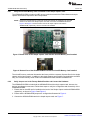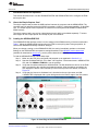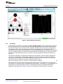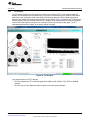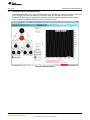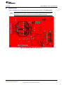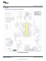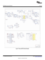
1
User's Guide
SBAU245A – June 2015 – Revised July 2015
ADS86xxEVM-PDK Evaluation Module
ADS86xxEVM-PDK
This user guide describes the operation and usage of the ADS86xx evaluation module (EVM). The
ADS86xx are a family of pin-compatible successive approximation (SAR) analog-to-digital converters
(ADCs) with varying resolution and channel counts designed for integrated data acquisition systems.
Table 1 lists the devices available in the ADS86xx family that are supported by the ADS86xxEVM.
Table 1. Devices Supported By the ADS86xxEVM
Device
Description
ADS8698
8-channel, integrated, 18-bit SAR ADC with ALARM
ADS8688A
8-channel, integrated, 16-bit SAR ADC with ALARM
ADS8678
8-channel, integrated, 14-bit SAR ADC with ALARM
ADS8668
8-channel, integrated, 12-bit SAR ADC with ALARM
Windows is a registered trademark of Microsoft Corporation.
SPI is a trademark of Motorola Mobility LLC.
Samtec is a trademark of Samtec Inc.
All other trademarks are the property of their respective owners.
SBAU245A – June 2015 – Revised July 2015
Submit Documentation Feedback
ADS86xxEVM-PDK Evaluation Module
Copyright © 2015, Texas Instruments Incorporated
1
www.ti.com
1
2
3
4
5
6
7
8
Contents
Related Documents.......................................................................................................... 4
ADS86xxEVM-PDK Overview .............................................................................................. 5
EVM Analog Interface ....................................................................................................... 6
3.1
Connecting Negative Inputs to Ground .......................................................................... 7
3.2
Using Onboard, Second-Order, Butterworth, Low-Pass Filters ............................................... 8
3.3
Selecting the Reference Mode for the ADS86xxEVM ......................................................... 8
Digital Interface .............................................................................................................. 9
4.1
Serial Interface (SPI) ............................................................................................... 9
4.2
I2C Bus for the Onboard EEPROM ............................................................................... 9
4.3
microSD Card ....................................................................................................... 9
Power Supplies ............................................................................................................. 10
ADS86xxEVM-PDK Initial Setup ......................................................................................... 12
6.1
Default Jumper Settings .......................................................................................... 12
6.2
Software Installation .............................................................................................. 13
ADS86xxEVM-PDK Kit Operation ........................................................................................ 19
7.1
About the Simple Capture Card ................................................................................. 19
7.2
Loading the ADS86xxEVM GUI ................................................................................. 19
7.3
Configuring the ADS86xxEVM................................................................................... 20
7.4
Capturing the Data ................................................................................................ 22
7.5
Analyzing the Data ................................................................................................ 26
7.6
Alarm Feature ...................................................................................................... 28
7.7
Phase Compensation ............................................................................................. 29
7.8
ADS86xxEVM GUI Simulation Mode ........................................................................... 31
Bill of Materials, Layout, and Schematics ............................................................................... 32
8.1
Bill of Materials .................................................................................................... 32
8.2
Board Layouts ..................................................................................................... 35
8.3
Schematics ......................................................................................................... 39
List of Figures
1
2
3
4
5
6
7
8
9
10
11
12
13
14
15
16
17
18
19
20
21
22
2
............................. 6
ADS86xxEVM Analog Input Connections for Channels AIN4, AIN5, AIN6, and AIN7 ............................. 6
Power-Supply Connections Diagram .................................................................................... 11
ADS86xxEVM Default Jumper Settings ................................................................................. 12
Bottom View of the Simple Capture Card with the microSD Memory Card Installed ............................. 14
Bottom View of the ADS86xxEVM Board with the microSD Memory Card Installed .............................. 14
Connecting the ADS86xxEVM Board to the Simple Capture Card .................................................. 15
LED Indicators on the Simple Capture Card............................................................................ 15
Destination Directory Screen ............................................................................................. 16
License Agreement Screen ............................................................................................... 16
Start Installation Screen ................................................................................................... 17
Progress Bar Screen ....................................................................................................... 17
Windows 7 Driver Installation Warning .................................................................................. 18
Installation Wizard Screen ................................................................................................ 18
Simple Capture Card Device Driver Completion ....................................................................... 18
Start Page of the ADS86xxEVM GUI .................................................................................... 19
System Block Diagram View .............................................................................................. 20
Selecting the Input Range for the Channels ............................................................................ 20
Register Map View ......................................................................................................... 21
ADS86xxEVM Jumper Settings .......................................................................................... 22
Manual Mode Data Capture .............................................................................................. 23
Data Capture in Auto Mode with Single Graph View .................................................................. 24
ADS86xxEVM Analog Input Connections for Channels AIN0, AIN1, AIN2, and AIN3
ADS86xxEVM-PDK Evaluation Module
SBAU245A – June 2015 – Revised July 2015
Submit Documentation Feedback
Copyright © 2015, Texas Instruments Incorporated
www.ti.com
23
Data Capture in Auto Mode with Multi Graph View .................................................................... 24
24
Saving the Captured Data................................................................................................. 25
25
Histogram Analysis ......................................................................................................... 26
26
FFT Analysis ................................................................................................................ 27
27
Alarm Enable Settings ..................................................................................................... 28
28
Phase Compensation Analysis ........................................................................................... 30
29
Simulation Mode ............................................................................................................ 31
30
ADS86xxEVM PCB: Top Layer (L1) ..................................................................................... 35
31
ADS86xxEVM PCB: Ground Layer (L2) ................................................................................. 36
32
ADS86xxEVM PCB: Analog Power Layer (L3) ......................................................................... 36
33
ADS86xxEVM PCB: Digital Power Layer (L4) .......................................................................... 37
34
ADS86xxEVM PCB: Ground Layer (L5) ................................................................................. 37
35
ADS86xxEVM PCB: Bottom Layer (L6) ................................................................................. 38
36
ADS86xx Interface Schematic ............................................................................................ 39
37
Power and SDCC Interface Schematic .................................................................................. 40
List of Tables
1
Devices Supported By the ADS86xxEVM ................................................................................ 1
2
Related Documentation ..................................................................................................... 4
3
J7: Analog Interface Connections
4
Connecting Negative Analog Inputs to Ground .......................................................................... 7
5
Using Onboard, Second-Order, Butterworth, Low-Pass Filters ........................................................ 8
6
Bypassing the Onboard, Second-Order, Butterworth, Low-Pass Filters.............................................. 8
7
Selecting the Reference for the ADS86xxEVM .......................................................................... 8
8
External Reference Connections .......................................................................................... 8
9
Connector J19 Pin Out ...................................................................................................... 9
10
Jumper Settings for Generating HVDD and HVSS Using an Onboard Switching Regulator..................... 10
11
Jumper Settings for Generating HVDD and HVSS from External High-Voltage Supplies ........................ 10
12
Power-Supply Connections ............................................................................................... 10
13
Default Jumper Configuration............................................................................................. 13
14
ADS8688EVM Bill of Materials
.........................................................................................
..........................................................................................
SBAU245A – June 2015 – Revised July 2015
Submit Documentation Feedback
ADS86xxEVM-PDK Evaluation Module
Copyright © 2015, Texas Instruments Incorporated
7
32
3
Related Documents
1
www.ti.com
Related Documents
Table 2 lists the related documents that are available through the Texas Instruments web site at
www.ti.com.
The ADS86xxEVM is designed to demonstrate true performance of these devices. Each input channel on
the selected device can support true bipolar input ranges of ±10.24 V, ±5.12 V, and ±2.56 V as well as
unipolar input ranges of 0 V to 10.24 V and 0 V to 5.12 V. The ADS8688A, ADS8678, and ADS8668
devices support additional true bipolar input ranges of ±1.28 V and ±0.64 V as well as unipolar input
ranges of 0 V to 2.56 V and 0 V to 1.28 V. The input range selection is done by software programming the
device internal registers. This selection is independent for each channel. The device offers a 1-MΩ,
constant resistive input impedance irrespective of the selected input range. This user guide includes circuit
description, a schematic diagram, and a bill of materials for the ADS86xxEVM circuit board.
Table 2. Related Documentation
4
Device
Literature Number
ADS8698
SBAS686
ADS8688A
SBAS680
ADS8678
SBAS627
ADS8668
SBAS492
OPA376
SBOS406
OPA2209
SBOS426
OPA320
SBOS513
REG71055
SBAS221
TPS7A4901
SBVS121
TPS54060
SLVS919
TPS7A3001
SBVS125
ADS86xxEVM-PDK Evaluation Module
SBAU245A – June 2015 – Revised July 2015
Submit Documentation Feedback
Copyright © 2015, Texas Instruments Incorporated
ADS86xxEVM-PDK Overview
www.ti.com
2
ADS86xxEVM-PDK Overview
The ADS86xxEVM-PDK is a platform for evaluating the ADS86xx series of devices. Throughout this
document, the terms ADS86xxEVM, demonstration kit, and evaluation board are synonyms with the
ADS8698EVM-PDK, ADS8688AEVM-PDK, ADS8678EVM-PDK, and ADS8668EVM-PDK. The
ADS86xxEVM-PDK consists of an ADS86xxEVM board and a simple capture card. The simple capture
card is a field-programmable gate array (FPGA)-based controller card that functions as a serial peripheral
interface (SPI™) host and transfers data to the ADS86xxEVM graphical user interface (GUI) via a USB
interface. The ADS86xxEVM GUI collects, analyzes, and records data from the ADS86xxEVM board. The
ADS86xxEVM GUI is capable of collecting data from the ADS86xxEVM in auto and manual modes,
configuring the ADC program registers, and performing FFT analysis of data captured from the ADC.
ADS86xxEVM Features:
• Includes support circuitry as a design example to match ADC performance.
• 3.3-V slave SPI.
• Serial interface header for easy connection to the simple capture card.
• Designed for a 5-V analog supply.
• Integrated 4.096-V voltage reference.
• Bipolar (±10.24 V, ±5,12 V, ±2.56 V, ±1.28 V, and ±0.64 V) or unipolar (0 V to 10.24 V, 0 V to 5.12 V,
0 V to 2.56 V, and 0 V to 1.28 V) input ranges for each channel.
• Onboard, second-order, Butterworth, low-pass filters for four channels.
• Onboard regulator for generating a ±15-V bipolar supply for second-order, Butterworth, low-pass filters.
• Accepts a ±100-mV signal on the negative analog inputs (AIN_xGND).
ADS86xxEVM GUI Features:
• Captures data from the ADS86xxEVM in auto and manual modes.
• Configures the ADS86xx device program registers.
• Enables and disables channels in auto mode.
• Provides FFT analysis and calculates the SNR, THD, and SINAD ac performance parameters.
• Provides single and multiple graph views for captured data.
• Includes a dc histogram for dc inputs.
• Logs ADC data.
SBAU245A – June 2015 – Revised July 2015
Submit Documentation Feedback
ADS86xxEVM-PDK Evaluation Module
Copyright © 2015, Texas Instruments Incorporated
5
EVM Analog Interface
3
www.ti.com
EVM Analog Interface
The ADS86xxEVM is designed for easy interfacing with analog sources. The Samtec™ connector
provides a convenient 10-pin, dual-row header at J7. Figure 1 and Figure 2 show the ADS86xxEVM
analog input connections for channels AIN0 to AIN3 and channels AIN4 to AIN7, respectively. Table 3 lists
the analog interface connections for J7.
Figure 1. ADS86xxEVM Analog Input Connections for Channels AIN0, AIN1, AIN2, and AIN3
Figure 2. ADS86xxEVM Analog Input Connections for Channels AIN4, AIN5, AIN6, and AIN7
6
ADS86xxEVM-PDK Evaluation Module
SBAU245A – June 2015 – Revised July 2015
Submit Documentation Feedback
Copyright © 2015, Texas Instruments Incorporated
EVM Analog Interface
www.ti.com
Table 3 summarizes the J7 analog interface connector.
Table 3. J7: Analog Interface Connections
3.1
Pin
Number
Signal
Description
J7.2
A6+
Positive analog input for channel AIN6
J7.4
A7+
Positive analog input for channel AIN7
J7.6
A0+
Positive analog input for channel AIN0
J7.8
A1+
Positive analog input for channel AIN1
J7.10
AUX+
Positive analog input for AUX channel
J7.12
A2+
Positive analog input for channel AIN2
J7.14
A3+
Positive analog input for channel AIN3
J7.16
A4+
Positive analog input for channel AIN4
J7.18
A5+
Positive analog input for channel AIN5
J7.20
GND
Analog ground connection
J7.1
A6–
Negative analog input for channel AIN6
J7.3
A7–
Negative analog input for channel AIN7
J7.5
A0–
Negative analog input for channel AIN0
J7.7
A1–
Negative analog input for channel AIN1
J7.9
AUX–
Connected to analog ground
J7.11
A2–
Negative analog input for channel AIN2
J7.13
A3–
Negative analog input for channel AIN3
J7.15
A4–
Negative analog input for channel AIN4
J7.17
A5–
Negative analog input for channel AIN5
J7.19
GND
Analog ground connection
Connecting Negative Inputs to Ground
The negative analog inputs for all channels (except for the AUX channel) are capable of accepting a ±100mV signal. The negative analog inputs can either be connected to the analog ground or a
±100-mV signal can be applied on these inputs. Table 4 describes the appropriate jumper settings for
connecting these inputs to analog ground.
Table 4. Connecting Negative Analog Inputs to Ground
Signal
Jumper
Position for Connecting to
Analog Ground
Position for Applying a ±100-mV Signal
A0–
J22
Closed
Open
A1–
J16
Closed
Open
A2–
J26
Closed
Open
A3–
J27
Closed
Open
A4–
J28
Closed
Open
A5–
J29
Closed
Open
A6–
J24
Closed
Open
A7–
J23
Closed
Open
AUX–
NA
Always connected to GND
NA
SBAU245A – June 2015 – Revised July 2015
Submit Documentation Feedback
ADS86xxEVM-PDK Evaluation Module
Copyright © 2015, Texas Instruments Incorporated
7
EVM Analog Interface
3.2
www.ti.com
Using Onboard, Second-Order, Butterworth, Low-Pass Filters
The ADS86xxEVM includes second-order, Butterworth, low-pass filters with a cutoff frequency of 22 kHz
for channels AIN0, AIN1, AIN2, and AIN3. There is also a provision to bypass these filters. See Figure 1
for an analog input circuit for channels AIN0, AIN1, AIN2, and AIN3. Table 5 lists the jumper settings for
using onboard, second-order, Butterworth, low-pass filters and Table 6 lists the jumper settings for
bypassing these filters.
Table 5. Using Onboard, Second-Order, Butterworth, Low-Pass Filters
Channel
Jumper
Position
Jumper
Position
AIN0
J25
Closed
J8
Closed between pins 1 and 2
AIN1
J31
Closed
J10
Closed between pins 1 and 2
AIN2
J30
Closed
J11
Closed between pins 2 and 3
AIN3
J15
Closed
J9
Closed between pins 2 and 3
Table 6. Bypassing the Onboard, Second-Order, Butterworth, Low-Pass Filters
3.3
Channel
Jumper
Position
Jumper
Position
AIN0
J25
AIN1
J31
Open
J8
Closed between pins 2 and 3
Open
J10
AIN2
Closed between pins 2 and 3
J30
Open
J11
Closed between pins 1 and 2
AIN3
J15
Open
J9
Closed between pins 1 and 2
Selecting the Reference Mode for the ADS86xxEVM
The ADS86xxEVM can either operate on an internal or external reference. Table 7 lists the jumper
settings for selecting the reference. Table 8 describes the connections for the external reference.
Table 7. Selecting the Reference for the ADS86xxEVM
Jumper
Position for Using Internal
Reference
Position for Using External Reference
J2
Closed
Open
Table 8. External Reference Connections
8
Pin
Number
Signal
Description
J5.1
REFIN
Input for external reference
J5.2
GND
Analog ground connection
ADS86xxEVM-PDK Evaluation Module
SBAU245A – June 2015 – Revised July 2015
Submit Documentation Feedback
Copyright © 2015, Texas Instruments Incorporated
Digital Interface
www.ti.com
4
Digital Interface
Connector J19 (Samtec part number ERF8-025-01-L-D-RZ-L-TR socket strip connector) provides the
digital I/O connections between the ADS86xxEVM board and the simple capture card. Consult Samtec at
www.samtec.com or call 1-800-SAMTEC-9 for a variety of mating connector options. Table 9 summarizes
the pin outs for connector J19.
Table 9. Connector J19 Pin Out
Pin Number
4.1
Signal
Description
J19.1
DAISY
J19.4
EVM_PRESENT
Daisy input for the ADC
J19.5
REFSEL
Reference selection input for the ADC
J19.6
RST/PD
Reset or power-down input for the ADC
J19.8
A
J19.11
EVM_ID_SDA
I2C data for the onboard EEPROM
J19.12
EVM_ID_SCL
I2C clock for the onboard EEPROM
J19.13
3V3_SDCC
3.3-V digital supply from the simple capture card
J19.14
5V_SDCC
Unregulated 5-V supply from the simple capture card
J19.33, J19.34
SCLK
EVM present, active low (connected to GND)
No connection
Clock input for the ADC
J19.35
CS
Chip-select input for the ADC
J19.38
SDI
Data input for the ADC
J19.39
SDO
Data output from the ADC
J19.45-49
EVMSDxxxxx
J19.2, J19.10, J19.16, J19.50
GND
Digital connections for the onboard micro secure digital
(microSD) card
Ground connections
Serial Interface (SPI)
The ADS86xx device uses SPI serial communication in mode 1 (CPOL = 0, CPHA = 1) with clock speeds
up to 18 MHz. The ADS86xxEVM offers 49.9-Ω resistors between the SPI signals and J19 to aid with
signal integrity. Typically, in high-speed SPI communication, fast signal edges can cause overshoot; these
49.9-Ω resistors slow down the signal edges in order to minimize signal overshoot.
4.2
I2C Bus for the Onboard EEPROM
The ADS86xxEVM has an I2C bus that records the board name and assembly date to communicate with
the onboard EEPROM. The bus is not used in any form by the ADS86xx converter.
4.3
microSD Card
The ADS86xxEVM has a microSD card that contains the software files for the simple capture card. The
contents of the microSD card must not be deleted or altered.
SBAU245A – June 2015 – Revised July 2015
Submit Documentation Feedback
ADS86xxEVM-PDK Evaluation Module
Copyright © 2015, Texas Instruments Incorporated
9
Power Supplies
5
www.ti.com
Power Supplies
The ADS86xxEVM can be powered from the simple capture card if onboard buffers for active low-pass
filters are not being used. The onboard regulator (U9) for generating high-voltage supplies (HVDD and
HVSS) is disabled by closing jumper J17. The HVDD and HVSS supplies are only required for buffers U4
and U5.
CAUTION
Do not open jumper J17 if the ADS86xxEVM must be powered only from the
simple capture card and an external 5-V supply is not provided on J32.
High-voltage supplies (HVDD and HVSS) for buffers U4 and U5 can be generated using the onboard
regulator (U9) if an external 5-V dc supply is provided on J32. The external 5-V dc supply must be at least
200 mV above the unregulated 5-V supply of the simple capture card. The external 5-V dc supply must be
capable of providing at least 500 mA of current. Table 10 provides jumper settings for generating HVDD
and HVSS using the onboard switching regulator U9.
Table 10. Jumper Settings for Generating HVDD and HVSS Using an Onboard Switching Regulator
Jumper
Position for Using an Onboard Switching Regulator
J12
Closed between pins 1 and 2
J14
Closed between pins 1 and 2
J17
Open
HVDD and HVSS for buffers U4 and U5 can also be generated by providing external high-voltage supplies
on J18, as shown in Table 11. Table 12 and Figure 3 illustrate the power-supply connections for external
supplies.
Table 11. Jumper Settings for Generating HVDD and HVSS from External High-Voltage Supplies
Jumper
Position for Generating HVDD and HVSS from External Voltage Supplies
J12
Closed between pins 2 and 3
J14
Closed between pins 2 and 3
J17
Closed
Table 12. Power-Supply Connections
Voltage
Supply
10
Signal
Voltage
Range
Pin Number
Note
External 5 V
EXT_5V
5 V to 5.5 V
J32.2
Required only for generating HVDD and HVSS using the
onboard switching regulator
—
GND
GND
J32.1
—
External HVDD
EXT_HVDD
16 V to 25 V
J18.3
Required only for generating HVDD and HVSS from external
high-voltage supplies. Make sure HVDD + |HVSS| < 36 V.
External HVSS
EXT_HVSS
–16 V to –25 V
J18.1
Required only for generating HVDD and HVSS from external
high-voltage supplies. Make sure HVDD + |HVSS| < 36 V.
—
GND
GND
J18.2
—
ADS86xxEVM-PDK Evaluation Module
SBAU245A – June 2015 – Revised July 2015
Submit Documentation Feedback
Copyright © 2015, Texas Instruments Incorporated
Power Supplies
www.ti.com
Figure 3. Power-Supply Connections Diagram
The AVDD analog supply for the ADS86xx is generated by converting an unregulated 5-V supply from the
simple capture card or by converting an external 5-V supply to a regulated 5-V supply by using the
REG71055 charge pump and the TPS7A4901 linear regulator. The DVDD digital supply for the ADC is
derived from a 3.3-V supply from the simple capture card.
SBAU245A – June 2015 – Revised July 2015
Submit Documentation Feedback
ADS86xxEVM-PDK Evaluation Module
Copyright © 2015, Texas Instruments Incorporated
11
ADS86xxEVM-PDK Initial Setup
6
www.ti.com
ADS86xxEVM-PDK Initial Setup
This section presents the steps required to setup the ADS86xxEVM-PDK kit prior to operation.
6.1
Default Jumper Settings
Figure 4 details the default jumper settings. Table 13 provides the configuration for these jumpers.
Figure 4. ADS86xxEVM Default Jumper Settings
12
ADS86xxEVM-PDK Evaluation Module
SBAU245A – June 2015 – Revised July 2015
Submit Documentation Feedback
Copyright © 2015, Texas Instruments Incorporated
ADS86xxEVM-PDK Initial Setup
www.ti.com
Table 13. Default Jumper Configuration
6.2
Jumper
Default Position
J2
Closed
J3
Open
J4
Closed
J5
Open
J6
Open
J8
Closed between pins 2 and 3
J9
Closed between pins 1 and 2
J10
Closed between pins 2 and 3
J11
Closed between pins 1 and 2
J12
Closed between pins 1 and 2
J13
Closed between pins 2 and 3
J14
Closed between pins 1 and 2
J15
Open
J16
Closed
J17
Closed
J21
Closed
J22
Closed
J23
Closed
J24
Closed
J25
Open
J26
Closed
J27
Closed
J28
Closed
J29
Closed
J30
Open
J31
Open
Software Installation
This section presents the steps required to the install the software.
NOTE: Ensure the microSD memory card included in the kit is installed in the microSD socket (P6)
on the back of the simple capture card before connecting the EVM to the computer.
Otherwise, as a result of improper boot up, Windows® cannot recognize the ADS86xxEVMPDK as a connected device.
Complete the following steps to install the software:
1. Verify the microSD memory cards are installed on the simple capture card and the ADS86xxEVM
board.
2. Verify jumpers are in the factory-default position and are properly connected to the hardware.
3. Install the ADS86xxEVM-PDK software.
4. Complete the simple capture card device driver installation.
Each task is described in the following subsections.
SBAU245A – June 2015 – Revised July 2015
Submit Documentation Feedback
ADS86xxEVM-PDK Evaluation Module
Copyright © 2015, Texas Instruments Incorporated
13
ADS86xxEVM-PDK Initial Setup
6.2.1
www.ti.com
Verify the microSD Memory Card is Installed on the Simple Capture Card
The ADS86xxEVM-PDK includes microSD memory cards that contain the EVM software and simple
capture card firmware required for the EVM operation.
NOTE: Ensure the microSD memory cards that contain the software are installed in the microSD
socket on the back of the simple capture card and on the back of ADS86xxEVM board.
Figure 5 and Figure 6 show the bottom view of the simple capture card and the
ADS86xxEVM, respectively, with the microSD card installed.
Figure 5. Bottom View of the Simple Capture Card with the microSD Memory Card Installed
Figure 6. Bottom View of the ADS86xxEVM Board with the microSD Memory Card Installed
The microSD memory cards are formatted at the factory with the necessary firmware files for the simple
capture card to boot properly. In addition to the simple capture card firmware files (application and MLO
files), the microSD memory cards contain the ADS86xxEVM-PDK software installation files.
6.2.2
Verify Jumpers are in the Factory-Default Position and Connect the Hardware
The ADS86xxEVM-PDK includes both the ADS86xxEVM and the simple capture card; however, the
devices are shipped unconnected. Follow these steps to verify the configuration and connectivity of the
ADS86xxEVM-PDK.
1. Ensure that he microSD card is installed on the back of the Simple Capture card and ADS86xxEVM
respectively, as shown in Figure 5 and Figure 6.
2. Ensure that the ADS86xxEVM jumpers are configured as illustrated in Figure 4.
3. Connect the ADS86xxEVM board to the simple capture card; see Figure 7.
14
ADS86xxEVM-PDK Evaluation Module
SBAU245A – June 2015 – Revised July 2015
Submit Documentation Feedback
Copyright © 2015, Texas Instruments Incorporated
ADS86xxEVM-PDK Initial Setup
www.ti.com
Figure 7. Connecting the ADS86xxEVM Board to the Simple Capture Card
4. Connect the simple capture card to the computer through the micro USB cable.
5. Verify that the LED D5 power-good indicator is illuminated. Wait approximately ten seconds and verify
that diode D2 blinks, indicating that USB communication with the host computer is functioning properly.
Figure 8 shows the location of the LED indicators in the simple capture card.
Figure 8. LED Indicators on the Simple Capture Card
6.2.3
Install the ADS86xxEVM-PDK Software
The ADS86xxEVM software must be installed on the computer. This software supports the ADS86xxEVMPDK. The user must have administrator privileges to install the EVM software. The following steps list the
directions to install the software.
1. Open the Windows explorer and locate the microSD memory card labeled ADS86xxEVM in the
browser as a removable storage device.
2. Navigate to the ...\ADS86xxEVMGUI\Version x.x\Volume\ folder.
3. Run the installer by double-clicking the setup.exe file. This action installs the EVM GUI software and
required simple capture card device driver components.
4. After the installer begins, a welcome screen is displayed. Click Next to continue.
5. Select the default directory under: ...\Program Files(x86)\Texas Instruments\ADS86XX EVM GUI\; see
Figure 9 and Figure 10. One or more software license agreements appear.
SBAU245A – June 2015 – Revised July 2015
Submit Documentation Feedback
ADS86xxEVM-PDK Evaluation Module
Copyright © 2015, Texas Instruments Incorporated
15
ADS86xxEVM-PDK Initial Setup
www.ti.com
Figure 9. Destination Directory Screen
Figure 10. License Agreement Screen
6. Select the I Accept the License Agreement radial button and click Next.
16
ADS86xxEVM-PDK Evaluation Module
SBAU245A – June 2015 – Revised July 2015
Submit Documentation Feedback
Copyright © 2015, Texas Instruments Incorporated
ADS86xxEVM-PDK Initial Setup
www.ti.com
7. The start installation screen appears, as shown in Figure 11. Click Next.
Figure 11. Start Installation Screen
8. A progress bar appears, as shown in Figure 12; this step takes a few minutes.
Figure 12. Progress Bar Screen
9. The progress bar is followed by an installation complete notice.
SBAU245A – June 2015 – Revised July 2015
Submit Documentation Feedback
ADS86xxEVM-PDK Evaluation Module
Copyright © 2015, Texas Instruments Incorporated
17
ADS86xxEVM-PDK Initial Setup
6.2.4
www.ti.com
Complete the Simple Capture Card Device Driver Installation
During installation of the simple capture card device driver, a prompt may appear with the Windows
security message shown in Figure 13. Select Install this driver software anyway to install the driver
required for proper operation of the software. The drivers contained within the installers are safe for
installation in your system.
Figure 13. Windows 7 Driver Installation Warning
NOTE: Driver installation prompts do not appear if the simple capture card device driver is already
installed on your system.
Following are the steps required to install the simple capture card device driver.
1. Immediately after the ADS86xxEVM software installation is complete, prompts appear to install the
simple capture card device driver; see Figure 14 and Figure 15.
2. A computer restart may be required to finish the software installation. If prompted, restart the computer
to complete the installation.
Figure 14. Installation Wizard Screen
18
Figure 15. Simple Capture Card Device Driver
Completion
ADS86xxEVM-PDK Evaluation Module
SBAU245A – June 2015 – Revised July 2015
Submit Documentation Feedback
Copyright © 2015, Texas Instruments Incorporated
ADS86xxEVM-PDK Kit Operation
www.ti.com
7
ADS86xxEVM-PDK Kit Operation
This section describes how to use the ADS86xxEVM-PDK and ADS86xxEVM GUI to configure the EVM
and acquire data.
7.1
About the Simple Capture Card
The simple capture card provides the USB interface between the computer and the ADS86xxEVM. The
controller board is designed around the AM335x processor, a USB 2.0, high-speed capability, 32-bit, ARM
core. The simple capture card incorporates an onboard FPGA subsystem and 256MB of onboard DDR
SRAM memory.
The simple capture card is not sold as a development board, and is not available separately. TI cannot
offer support for the simple capture card except as part of this EVM kit.
7.2
Loading the ADS86xxEVM GUI
The ADS86xxEVM GUI provides control over the settings of the ADS86xx family of devices mentioned in
Table 1. Adjust the ADS86xxEVM settings when the EVM is not acquiring data. During acquisition, all
controls are disabled and settings cannot be changed.
When you change a setting on the ADS86xxEVM GUI, the setting immediately updates on the board.
Settings on the ADS86xxEVM correspond to settings described in the ADS86xx product data sheet
(available for download at www.ti.com); see the product data sheet for details.
To load the ADS86xxEVM GUI, follow these steps:
Step 1. Make sure the PDK kit is configured and powered up as explained in Section 6.2.2.
Step 2. Start the ADS86xxEVM GUI. Go to Start→All Programs→Texas Instruments→ADS86xx EVM
GUI and click ADS86xx EVM GUI to run the software.
Step 3. Verify that the software detects the ADS86xxEVM. The GUI identifies the device on the EVM
that is connected to the controller and loads the settings. After the settings are loaded, the
GUI displays the device name followed by EVM on the top of the GUI window, as shown in
Figure 16.
Step 4. Verify that the Connect to Hardware box is checked on the top right corner and HW
CONNECTED is displayed with a green background on the bottom edge of the GUI window.
Figure 16. Start Page of the ADS86xxEVM GUI
SBAU245A – June 2015 – Revised July 2015
Submit Documentation Feedback
ADS86xxEVM-PDK Evaluation Module
Copyright © 2015, Texas Instruments Incorporated
19
ADS86xxEVM-PDK Kit Operation
7.3
7.3.1
www.ti.com
Configuring the ADS86xxEVM
System Block Diagram View
The ADS86xx channels can be configured by the system block diagram view in the GUI. The system block
diagram can be activated by clicking on the Program Register button on the left side of the GUI window.
A channel can be powered down by checking the AINx_PD box. if a channel is powered down, that
channel turns grey in system block view. The voltage range for each channel can be selected from a dropdown menu corresponding to each channel in the system block diagram view, as shown in Figure 17. The
window for selecting the input voltage range is displayed in Figure 18.
Figure 17. System Block Diagram View
Figure 18. Selecting the Input Range for the Channels
20
ADS86xxEVM-PDK Evaluation Module
SBAU245A – June 2015 – Revised July 2015
Submit Documentation Feedback
Copyright © 2015, Texas Instruments Incorporated
ADS86xxEVM-PDK Kit Operation
www.ti.com
7.3.2
Register Map View
All registers can be read or written by the register map view in the GUI. The register map view can be
activated by clicking the Register Map View button in the system block diagram view; see Figure 17. The
register map table provides a complete list of program registers present in the ADS86xx device. The user
must provide data in hexadecimal for writing registers. The user also must select the register in the
register map, provide data in the Write Data box, and click the Write Register button to write the register.
For reading a register, the user must select the register in the register map and click the Read Register
button. All registers can be read by clicking the Read All button. The values for all registers can be saved
in a configuration file (.cfg) by the Save Config button. The saved configuration can be loaded back by
using the Load Config button. Changes made in the register map view are reflected in the system block
view and vice-versa. For details on the ADS86xx program registers, refer to the program register map in
the respective device data sheet. Figure 19 shows the register map view.
Figure 19. Register Map View
SBAU245A – June 2015 – Revised July 2015
Submit Documentation Feedback
ADS86xxEVM-PDK Evaluation Module
Copyright © 2015, Texas Instruments Incorporated
21
ADS86xxEVM-PDK Kit Operation
7.3.3
www.ti.com
Jumper Settings for the ADS86xxEVM
The ADS86xxEVM Settings button on the left side of the GUI window describes the jumper settings on
the ADS86xxEVM. The reset and REFSEL jumpers are monitored by the GUI. If the reset jumper (J3) is
open, the GUI switches to the reset Program mode in the start page of the GUI. For details on different
jumper settings; see Section 3 and Section 5. Figure 20 shows the ADS86xxEVM GUI window for the
jumper settings.
Figure 20. ADS86xxEVM Jumper Settings
7.4
Capturing the Data
Data can be captured from the ADS86xxEVM either in manual mode or in auto mode. Manual mode
captures data from one of the device channels whereas auto mode captures data from the channels that
are powered up and selected in the auto channel sequence. Section 7.4.1 and Section 7.4.2 provide
details for manual and auto mode, respectively.
7.4.1
Manual Mode
Manual mode can be activated by clicking on the Manual Channel N button on the left side of the GUI
window and by selecting Data Capture from the drop-down menu; see Figure 21. In manual mode, data
are captured for the channel selected by the Channel Name drop-down menu. The sampling rate and
number of samples for the data capture can be entered in the ADC Capture Settings box. The
ADS86xxEVM GUI supports a sampling rate from 20 kSPS to 500 kSPS. The sampling rate is adjusted to
the closest value obtained from Equation 1.
Sampling Rate (kSPS) = 17000 / [34 + K] ......... for the ADS8688A, ADS8678, and ADS8668 Devices
Sampling Rate (kSPS) = 18000 / [36 + K] ........ for the ADS8698 device
(1)
where
•
0 ≤ K ≤ 816, and K is an integer.
(2)
The GUI supports a capture of 1024 samples to 8,388,608 samples. For sampling rates less than
100 kSPS, the maximum number of samples are limited to 131,072 per capture. The number of samples
are adjusted to the closest power of 2. The data captured are displayed in a graph in the GUI window.
22
ADS86xxEVM-PDK Evaluation Module
SBAU245A – June 2015 – Revised July 2015
Submit Documentation Feedback
Copyright © 2015, Texas Instruments Incorporated
ADS86xxEVM-PDK Kit Operation
www.ti.com
Figure 21. Manual Mode Data Capture
7.4.2
Auto Mode
Auto mode can be activated by clicking on the Auto with Reset Mode button and selecting Data Capture
from the drop-down menu. In auto mode, data are captured sequentially for the channel selected in the
auto channel sequence. The channels can be enabled or disabled by the check boxes corresponding to
the channels. In auto mode, the sampling rate entered is an aggregate of the sampling rate for all
channels enabled in the auto channel sequence. The effective sampling rate for a channel is the sampling
rate for the device divided by the number of channels enabled. The sampling rate for the device must be
entered in the Sample Rate (ksps) box. Also in auto mode, the sampling rate follows the calculation of
Equation 1.
The number of samples to be captured per channel must be entered in the ADC Capture Settings box.
The number of samples per channel value is adjusted to the closest power of 2 by the GUI. The GUI
supports a maximum capture of 8,388,608 samples per capture. The maximum number of samples per
channel that can be captured in auto mode is determined by Equation 3.
(Number of Samples per Channel) × (Number of Channels Enabled) ≤ 8,388,608
(3)
Data captured in auto mode can be viewed in single graph view or in multi graph view. In single graph
view, data for an individual channel are displayed in a single graph. The channel for a single graph can be
selected from the channel drop-down menu. In multi graph view, data for all enabled channels are
displayed in multi graph view. Figure 22 and Figure 23 illustrate the data captured in auto mode.
SBAU245A – June 2015 – Revised July 2015
Submit Documentation Feedback
ADS86xxEVM-PDK Evaluation Module
Copyright © 2015, Texas Instruments Incorporated
23
ADS86xxEVM-PDK Kit Operation
www.ti.com
Figure 22. Data Capture in Auto Mode with Single Graph View
Figure 23. Data Capture in Auto Mode with Multi Graph View
24
ADS86xxEVM-PDK Evaluation Module
SBAU245A – June 2015 – Revised July 2015
Submit Documentation Feedback
Copyright © 2015, Texas Instruments Incorporated
ADS86xxEVM-PDK Kit Operation
www.ti.com
7.4.3
Saving the Captured Data
The data captured from the EVM can be stored in a .csv file by clicking the Log Data To File button, as
shown in Figure 24. A window appears for selecting the location and entering the name of the file for
saving the captured data.
Figure 24. Saving the Captured Data
SBAU245A – June 2015 – Revised July 2015
Submit Documentation Feedback
ADS86xxEVM-PDK Evaluation Module
Copyright © 2015, Texas Instruments Incorporated
25
ADS86xxEVM-PDK Kit Operation
7.5
www.ti.com
Analyzing the Data
The ADS86xxEVM GUI includes the histogram analysis and FFT analysis for data captured from the
ADS86xxEVM in auto or manual mode. Data can be analyzed with the selected analysis from the dropdown menu in the ADC capture settings.
7.5.1
Histogram Analysis
Histogram testing is commonly used when testing ADCs. A histogram is merely a count of the number of
times a code occurs in a particular data set. The histogram analysis page of the GUI creates a histogram
of the data of the acquired data set and displays that data. The input channel (AINx) for the histogram
analysis can be selected from the channel drop-down menu and the data capture settings can be entered
in boxes on the left side of the graph. Figure 25 shows the histogram analysis page.
Figure 25. Histogram Analysis
The following parameters are calculated using the histogram analysis.
• Code Spread: Is the number of different codes captured for a certain input.
• Code Peak: Is the code with the maximum number of hits.
• Sigma: Is the standard deviation of all the codes captured.
• Mean: Is the average of all the codes captured for a certain input.
26
ADS86xxEVM-PDK Evaluation Module
SBAU245A – June 2015 – Revised July 2015
Submit Documentation Feedback
Copyright © 2015, Texas Instruments Incorporated
ADS86xxEVM-PDK Kit Operation
www.ti.com
7.5.2
FFT Analysis
The FFT analysis page in the GUI performs the fast fourier transform (FFT) of the captured data and
displays the resulting frequency domain plots. This page also calculates key ADC dynamic performance
parameters, such as signal-to-noise ratio (SNR), total harmonic distortion (THD), signal-to-noise and
distortion ratio (SINAD), and spurious-free dynamic range (SFDR). Figure 26 shows the FFT performance
analysis display. The input channel (AINx) for FFT analysis can be selected from the channel drop-down
menu and the data capture settings can be entered in boxes on the left side of the graph. The FFT
calculated parameters are shown on the bottom side of the graph.
Figure 26. FFT Analysis
Input signal frequency for FFT analysis:
• The GUI analyses the FFT to provide signal power (dBFs), SNR, SINAD, THD, SFDR, and ENOB
numbers.
• The GUI uses a 7-term Blackman-Harris window to minimize spectral leakage.
SBAU245A – June 2015 – Revised July 2015
Submit Documentation Feedback
ADS86xxEVM-PDK Evaluation Module
Copyright © 2015, Texas Instruments Incorporated
27
ADS86xxEVM-PDK Kit Operation
7.6
7.6.1
www.ti.com
Alarm Feature
Alarm Functionality
The ADS86xx series of devices support an elaborate set of ALARM functionality. The detail of the ALARM
functionality and operation is available in respective device data sheets. The ADS86xxEVM and GUI
support the required hardware and software features to demonstrate the ALARM functionality of the
device.
The ALARM feature of the device can be activated by clicking the Edit Alarm Limits button when in
manual or auto mode. Individual channel threshold levels and hysteresis levels can be programmed in the
Configure Alarm Settings pop-up window. The ALARM feature can be enabled or disabled by checking or
unchecking the Alarm Enable? check box. Click the Config Alarm Settings button to program device
registers with correct data, as shown in Figure 27.
The user can also program these values by individually programming each register from register map
view, as described in Section 7.3.2.
Figure 27. Alarm Enable Settings
28
ADS86xxEVM-PDK Evaluation Module
SBAU245A – June 2015 – Revised July 2015
Submit Documentation Feedback
Copyright © 2015, Texas Instruments Incorporated
ADS86xxEVM-PDK Kit Operation
www.ti.com
When the ALARM feature is enabled, the capture data window shows the indicators for high and low
thresholds based on the values programmed. After data capture, if the device detects an ALARM event,
EVM diode D1 turns on with a red indicator light. The GUI monitors the status of the ALARM pin on the
device. When an ALARM is detected, the ALARM indicator on the GUI starts flashing.
The user can read the status of tripped alarms by clicking the Diagnose Alarm? button. The user can
also read the ALARM register contents from register map view to detect the state of tripped and active
alarms.
7.7
Phase Compensation
The ADS86xxEVM GUI includes an analysis page for compensating the phase of signals captured in auto
mode. When the signals on different channels are sampled in auto mode, a deterministic phase difference
between signals is introduced resulting from the time difference between sampling instants. The phase
difference is dependent on sampling rate, input signal frequency, number of channels, and initial phase
difference. The phase compensation analysis page compensates for the introduced phase difference and
provides the results after phase compensation. For details on phase compensation, see the reference
guide Phase Compensated 8-CH Multiplexed Data Acquisition System for Power Automation (TIDU427).
The phase compensation analysis page can be activated from the Smart App menu. Figure 28 displays
the phase compensation analysis page.
SBAU245A – June 2015 – Revised July 2015
Submit Documentation Feedback
ADS86xxEVM-PDK Evaluation Module
Copyright © 2015, Texas Instruments Incorporated
29
ADS86xxEVM-PDK Kit Operation
www.ti.com
Figure 28. Phase Compensation Analysis
30
ADS86xxEVM-PDK Evaluation Module
SBAU245A – June 2015 – Revised July 2015
Submit Documentation Feedback
Copyright © 2015, Texas Instruments Incorporated
ADS86xxEVM-PDK Kit Operation
www.ti.com
7.8
ADS86xxEVM GUI Simulation Mode
The ADS86xxEVM GUI can be run in simulation mode by unchecking the Connect to Hardware check-box
on the top right side of the GUI window. In simulation mode, the GUI does not connect to the
ADS86xxEVM board and only displays the results for one set of captured data stored in the computer.
Figure 29 shows the ADS86xxEVM GUI running in simulation mode.
Figure 29. Simulation Mode
SBAU245A – June 2015 – Revised July 2015
Submit Documentation Feedback
ADS86xxEVM-PDK Evaluation Module
Copyright © 2015, Texas Instruments Incorporated
31
Bill of Materials, Layout, and Schematics
8
www.ti.com
Bill of Materials, Layout, and Schematics
Schematics for the ADS86xxEVM are appended to this user's guide. The bill of material is the same for all devices in the ADS86xx family. The
device U2 varies based on the device chosen for evaluation. The bill of materials is provided in Table 14. Section 8.2 shows the PCB layouts for
the ADS86xxEVM with the ADS8688IDBT device installed on the EVM. Section 8.3 provides the schematics for the ADS86xxEVM and
ADS8688IDBT.
8.1
Bill of Materials
NOTE: All components are compliant with the European Union Restriction on Use of Hazardous Substances (RoHS) Directive. Some part
numbers may be either leaded or RoHS. Verify that purchased components are RoHS-compliant. (For more information about TI's
position on RoHS compliance, see www.ti.com.)
Table 14. ADS8688EVM Bill of Materials
Item No.
Qty
Ref Des
1
1
!PCB
2
4
3
4
32
Description
Vendor
Part Number
Printed Circuit Board
Any
PRJ_Number
C1-C3, C6
CAP, CERM, 0.1uF, 25V, +/-5%, X7R, 0603
AVX
06033C104JAT2A
1
C10
CAP, CERM, 1uF, 16V, +/-10%, X5R, 0603
1
C11
CAP, CERM, 3000pF, 50V, +/-5%, C0G/NP0, 0603
5
6
C16, C24, C26, C30, C45, C64
CAP, CERM, 0.1uF, 50V, +/-10%, X7R, 0603
AVX
06035C104KAT2A
6
4
C17, C22, C27, C28
CAP, CERM, 2200pF, 50V, +/-5%, C0G/NP0, 0603
TDK
C1608C0G1H222J
7
4
C23, C25, C29, C31
CAP, CERM, 1000pF, 50V, +/-5%, C0G/NP0, 0402
MuRata
GRM1555C1H102JA01D
8
4
C32, C35, C49, C50
CAP, CERM, 22uF, 25V, +/-10%, X7R, 1210
MuRata
GRM32ER71E226KE15L
9
3
C34, C36, C53
CAP, CERM, 10uF, 25V, +/-10%, X7R, 1206
MuRata
GRM31CR71E106KA12L
10
2
C37, C54
CAP, CERM, 10uF, 35V, +/-10%, X7R, 1206
Taiyo Yuden
GMK316AB7106KL
11
15
C4, C12-C15, C18-C21, C38-C41, C56,
C58
TDK
C1608C0G1H103J080AA
12
1
C42
CAP, CERM, 0.22uF, 16V, +/-10%, X7R, 0603
TDK
C1608X7R1C224K
13
2
C44, C46
CAP, CERM, 2.2uF, 10V, +/-10%, X7R, 0603
MuRata
GRM188R71A225KE15D
14
1
C48
CAP, CERM, 10uF, 50V, +/-20%, X7R, 2220
TDK
C5750X7R1H106M
15
1
C5
CAP, CERM, 10uF, 6.3V, +/-20%, X5R, 0603
Kemet
C0603C106M9PACTU
16
1
C51
CAP, CERM, 0.1uF, 25V, +/-5%, X7R, 0603
Kemet
C0603C104J3RAC
17
1
C52
CAP, CERM, 0.39uF, 16V, +/-10%, X7R, 0603
MuRata
GRM188R71C394KA88D
18
1
C57
CAP, CERM, 470pF, 50V, +/-10%, X7R, 0603
TDK
C1608X7R1H471K
19
2
C59, C60
CAP, CERM, 10uF, 35V, +/-10%, X7R, 1210
MuRata
GRM32ER7YA106KA12L
20
7
C7, C33, C43, C47, C55, C61, C62
CAP, CERM, 10uF, 10V, +/-10%, X7R, 0805
MuRata
GRM21BR71A106KE51L
21
1
C8
CAP, CERM, 22uF, 16V, +/-20%, X7R, 1210
TDK
C3225X7R1C226M
22
2
C9, C63
CAP, CERM, 1uF, 16V, +/-10%, X7R, 0603
TDK
C1608X7R1C105K
23
1
D1
Lite On
LTST-C170UKT
CAP, 10000pF, 0603, 5%, 50V, C0G
Diode, LED, RED, 2.1V, 14.2-mcd, 20 mA, 0805
ADS86xxEVM-PDK Evaluation Module
Kemet
C0603C105K4PACTU
MuRata
GRM1885C1H302JA01D
SBAU245A – June 2015 – Revised July 2015
Submit Documentation Feedback
Copyright © 2015, Texas Instruments Incorporated
Bill of Materials, Layout, and Schematics
www.ti.com
Table 14. ADS8688EVM Bill of Materials (continued)
Item No.
Qty
Ref Des
24
2
D2, D4
Diode, Schottky, 60V, 2A, SMA
Description
25
2
D3, D5
26
2
27
1
28
2
D9, D10
29
6
FID1-FID6
30
4
31
32
Vendor
Part Number
Diodes Inc.
B260A-13-F
Diode, Zener, 5.6V, 500mW, SOD-123
ON Semiconductor
MMSZ4690T1G
D6, D8
Diode, Zener, 27V, 500mW, SOD-123
Vishay-Semiconductor
MMSZ4711-V
D7
Diode, Zener, 3.9V, 500mW, SOD-123
ON Semiconductor
MMSZ4686T1G
Diodes Inc.
BAT54C-7-F
Diode, Schottky, 30V, 0.2A, SOT-23
Fiducial mark. There is nothing to buy or mount.
N/A
N/A
H1-H4
Bumpon, Hex, 0.063mil, 11mm Dia, Lt Brn
3M
SJ5202
2
J1, J7
Header, 100mil, 10x2, SMD
Samtec, Inc.
TSM-110-01-T-DV-P
1
J18
Terminal Block, 6A, 3.5mm Pitch, 3-Pos, TH
33
1
J19
34
19
J2-J6, J15-J17, J21-J31
35
1
J20
36
2
J32, J33
37
7
J8-J14
38
1
L1
—
Wurth Electronics
744870471
39
1
Q1
Transistor, NPN, 45V, 0.1A, SOT-23
ON Semiconductor
BC847CLT1G
40
8
R1, R79-R85
RES, 10.0k ohm, 1%, 0.063W, 0402
Vishay-Dale
CRCW040210K0FKED
41
5
R11, R21, R22, R74, R76
RES, 10.0Meg ohm, 1%, 0.063W, 0402
Vishay-Dale
CRCW040210M0FKED
42
1
R12
RES, 1.0k ohm, 5%, 0.125W, 0805
Vishay-Dale
CRCW08051K00JNEA
43
3
R13, R15, R18
RES, 47.0k ohm, 1%, 0.1W, 0603
Yageo America
RC0603FR-0747KL
44
1
R17
RES, 220k ohm, 5%, 0.063W, 0402
Vishay-Dale
CRCW0402220KJNED
On-Shore Technology, Inc.
ED555/3DS
Receptacle, Micro High Speed Socket Strip, 0.8mm, 25x2, R/A, SMT
Samtec, Inc.
ERF8-025-01-L-D-RA-L-TR
Header, TH, 100mil, 2x1, Gold plated, 230 mil above insulator
Samtec, Inc.
TSW-102-07-G-S
Molex
502570-0893
MicroSD Memory Card Connector
Terminal Block, 6A, 3.5mm Pitch, 2-Pos, TH
Header, TH, 100mil, 3x1, Gold plated, 230 mil above insulator
On-Shore Technology, Inc.
ED555/2DS
Samtec, Inc.
TSW-103-07-G-S
45
1
R19
RES, 100 ohm, 1%, 0.1W, 0603
Vishay-Dale
CRCW0603100RFKEA
46
17
R2, R3, R5-R10, R14, R16, R86-R91, R93
RES, 49.9 ohm, 1%, 0.063W, 0402
Vishay-Dale
CRCW040249R9FKED
47
1
R20
RES, 100k ohm, 1%, 0.063W, 0402
Vishay-Dale
CRCW0402100KFKED
48
16
R23-R32, R34, R35, R37, R38, R40, R41
RES, 357 ohm, 1%, 0.063W, 0402
Vishay-Dale
CRCW0402357RFKED
49
13
R36, R44, R48, R52, R94-R96, R98-R100,
R102, R103, R107
Resistor, Uninstalled
NI
NI
50
16
R4, R33, R39, R47, R49, R61, R69, R77,
R78, R92, R97, R101, R104-R106, R108
RES, 0 ohm, 5%, 0.063W, 0402
Yageo America
RC0402JR-070RL
51
4
R42, R46, R50, R54
RES, 3.57k ohm, 1%, 0.063W, 0402
Vishay-Dale
CRCW04023K57FKED
52
4
R43, R45, R51, R53
RES, 6.65k ohm, 1%, 0.063W, 0402
Vishay-Dale
CRCW04026K65FKED
53
1
R55
RES, 576k ohm, 1%, 0.063W, 0402
Vishay-Dale
CRCW0402576KFKED
54
2
R56, R71
RES, 232k ohm, 1%, 0.063W, 0402
Vishay-Dale
CRCW0402232KFKED
55
1
R57
RES, 182k ohm, 1%, 0.063W, 0402
Vishay-Dale
CRCW0402182KFKED
56
4
R58, R60, R62, R72
RES, 499k ohm, 1%, 0.063W, 0402
Vishay-Dale
CRCW0402499KFKED
57
2
R59, R73
RES, 20k ohm, 5%, 0.063W, 0402
Vishay-Dale
CRCW040220K0JNED
58
1
R63
RES, 33k ohm, 5%, 0.063W, 0402
Vishay-Dale
CRCW040233K0JNED
SBAU245A – June 2015 – Revised July 2015
Submit Documentation Feedback
ADS86xxEVM-PDK Evaluation Module
Copyright © 2015, Texas Instruments Incorporated
33
Bill of Materials, Layout, and Schematics
www.ti.com
Table 14. ADS8688EVM Bill of Materials (continued)
Item No.
Qty
Ref Des
Vendor
Part Number
59
2
R64, R75
RES, 82k ohm, 5%, 0.063W, 0402
Vishay-Dale
CRCW040282K0JNED
60
1
R65
RES, 15k ohm, 5%, 0.063W, 0402
Vishay-Dale
CRCW040215K0JNED
61
1
R66
RES, 1.1k ohm, 5%, 0.063W, 0402
Vishay-Dale
CRCW04021K10JNED
62
1
R67
RES, 44.2k ohm, 1%, 0.063W, 0402
Vishay-Dale
CRCW040244K2FKED
63
1
R68
RES, 412k ohm, 1%, 0.063W, 0402
Vishay-Dale
CRCW0402412KFKED
64
1
R70
RES, 20.5k ohm, 1%, 0.063W, 0402
Vishay-Dale
CRCW040220K5FKED
65
1
SD1
SanDisk MicroSD Card, 2GB
SanDisk
SDSDQ-002G
66
26
SH-J2-SH-J6, SH-J8-SH-J17,
SH-J21-SH-J31
3M
969102-0000-DA
67
1
TP11
Test Point, Miniature, Black, TH
Keystone
5001
68
6
TP12-TP17
Test Point, Miniature, Red, TH
Keystone
5000
69
9
TP2-TP10
Test Point, Miniature, White, TH
Keystone
5002
70
2
U1, U3
Op Amp, Precision, 5.5MHz, Low-Noise, RRIO, with e-trim
Texas Instruments
OPA376AIDBVR
71
1
U10
IC, -3V to -36V, -200mA, Ultralow Noise, High-PSRR LDO Negative
Linear Regulator
Texas Instruments
TPS7A3001DGN
72
1
U11
IC, 2K, Serial EEPROM
Atmel
AT24C02B
73
1
U2
16 bit 500KSPS 8 Channel SAR ADC
Texas Instruments
ADS8688IDBT
74
2
U4, U5
OpAmp, Low Noise, Low Power, 36V
Texas Instruments
OPA2209AIDGKR
75
2
U6, U7
IC, VIN 3V to 35V, 150mA, Ultralow Noise, High-PSRR, LDO
Regulator
Texas Instruments
TPS7A4901DGN
76
1
U8
IC, SWITCHED CAP, BUCK BOOST CONVERTER 1.8V to 5.5V in
65uA
Texas Instruments
REG71055DDC
77
1
U9
Buck Inverting Buck-Boost Step Down Regulator with 3.5 to 60 V
Input and 0.8 to 58 V Output, -40 to 150 degC, 10-Pin MSOPPowerPAD (DGQ), Green (RoHS & no Sb/Br)
Texas Instruments
TPS54060DGQ
34
Description
Shunt, 100mil, Gold plated, Black
ADS86xxEVM-PDK Evaluation Module
SBAU245A – June 2015 – Revised July 2015
Submit Documentation Feedback
Copyright © 2015, Texas Instruments Incorporated
Bill of Materials, Layout, and Schematics
www.ti.com
8.2
Board Layouts
Figure 30 through Figure 35 show the printed circuit board (PCB) layouts for the ADS86xxEVM.
NOTE: Board layouts are not to scale. These figures are intended to show how the board is laid out;
these figures are not intended to be used for manufacturing ADS86xxEVM PCBs.
Figure 30. ADS86xxEVM PCB: Top Layer (L1)
SBAU245A – June 2015 – Revised July 2015
Submit Documentation Feedback
ADS86xxEVM-PDK Evaluation Module
Copyright © 2015, Texas Instruments Incorporated
35
Bill of Materials, Layout, and Schematics
www.ti.com
Figure 31. ADS86xxEVM PCB: Ground Layer (L2)
Figure 32. ADS86xxEVM PCB: Analog Power Layer (L3)
36
ADS86xxEVM-PDK Evaluation Module
SBAU245A – June 2015 – Revised July 2015
Submit Documentation Feedback
Copyright © 2015, Texas Instruments Incorporated
Bill of Materials, Layout, and Schematics
www.ti.com
Figure 33. ADS86xxEVM PCB: Digital Power Layer (L4)
Figure 34. ADS86xxEVM PCB: Ground Layer (L5)
SBAU245A – June 2015 – Revised July 2015
Submit Documentation Feedback
ADS86xxEVM-PDK Evaluation Module
Copyright © 2015, Texas Instruments Incorporated
37
Bill of Materials, Layout, and Schematics
www.ti.com
Figure 35. ADS86xxEVM PCB: Bottom Layer (L6)
38
ADS86xxEVM-PDK Evaluation Module
SBAU245A – June 2015 – Revised July 2015
Submit Documentation Feedback
Copyright © 2015, Texas Instruments Incorporated
Bill of Materials, Layout, and Schematics
www.ti.com
8.3
Schematics
Figure 36 and Figure 37 illustrate schematics for the ADS86xxEVM-PDK.
Figure 36. ADS86xx Interface Schematic
SBAU245A – June 2015 – Revised July 2015
Submit Documentation Feedback
ADS86xxEVM-PDK Evaluation Module
Copyright © 2015, Texas Instruments Incorporated
39
Bill of Materials, Layout, and Schematics
www.ti.com
Figure 37. Power and SDCC Interface Schematic
40
ADS86xxEVM-PDK Evaluation Module
SBAU245A – June 2015 – Revised July 2015
Submit Documentation Feedback
Copyright © 2015, Texas Instruments Incorporated
Revision History
www.ti.com
Revision History
Changes from Original (June 2015) to A Revision ......................................................................................................... Page
•
•
•
Added title to Related Documents section ............................................................................................. 4
Added reference to Section 8.3 in overview of Section 8 .......................................................................... 32
Added Schematics section ............................................................................................................. 39
NOTE: Page numbers for previous revisions may differ from page numbers in the current version.
SBAU245A – June 2015 – Revised July 2015
Submit Documentation Feedback
Revision History
Copyright © 2015, Texas Instruments Incorporated
41
STANDARD TERMS AND CONDITIONS FOR EVALUATION MODULES
1.
Delivery: TI delivers TI evaluation boards, kits, or modules, including any accompanying demonstration software, components, or
documentation (collectively, an “EVM” or “EVMs”) to the User (“User”) in accordance with the terms and conditions set forth herein.
Acceptance of the EVM is expressly subject to the following terms and conditions.
1.1 EVMs are intended solely for product or software developers for use in a research and development setting to facilitate feasibility
evaluation, experimentation, or scientific analysis of TI semiconductors products. EVMs have no direct function and are not
finished products. EVMs shall not be directly or indirectly assembled as a part or subassembly in any finished product. For
clarification, any software or software tools provided with the EVM (“Software”) shall not be subject to the terms and conditions
set forth herein but rather shall be subject to the applicable terms and conditions that accompany such Software
1.2 EVMs are not intended for consumer or household use. EVMs may not be sold, sublicensed, leased, rented, loaned, assigned,
or otherwise distributed for commercial purposes by Users, in whole or in part, or used in any finished product or production
system.
2
Limited Warranty and Related Remedies/Disclaimers:
2.1 These terms and conditions do not apply to Software. The warranty, if any, for Software is covered in the applicable Software
License Agreement.
2.2 TI warrants that the TI EVM will conform to TI's published specifications for ninety (90) days after the date TI delivers such EVM
to User. Notwithstanding the foregoing, TI shall not be liable for any defects that are caused by neglect, misuse or mistreatment
by an entity other than TI, including improper installation or testing, or for any EVMs that have been altered or modified in any
way by an entity other than TI. Moreover, TI shall not be liable for any defects that result from User's design, specifications or
instructions for such EVMs. Testing and other quality control techniques are used to the extent TI deems necessary or as
mandated by government requirements. TI does not test all parameters of each EVM.
2.3 If any EVM fails to conform to the warranty set forth above, TI's sole liability shall be at its option to repair or replace such EVM,
or credit User's account for such EVM. TI's liability under this warranty shall be limited to EVMs that are returned during the
warranty period to the address designated by TI and that are determined by TI not to conform to such warranty. If TI elects to
repair or replace such EVM, TI shall have a reasonable time to repair such EVM or provide replacements. Repaired EVMs shall
be warranted for the remainder of the original warranty period. Replaced EVMs shall be warranted for a new full ninety (90) day
warranty period.
3
Regulatory Notices:
3.1 United States
3.1.1
Notice applicable to EVMs not FCC-Approved:
This kit is designed to allow product developers to evaluate electronic components, circuitry, or software associated with the kit
to determine whether to incorporate such items in a finished product and software developers to write software applications for
use with the end product. This kit is not a finished product and when assembled may not be resold or otherwise marketed unless
all required FCC equipment authorizations are first obtained. Operation is subject to the condition that this product not cause
harmful interference to licensed radio stations and that this product accept harmful interference. Unless the assembled kit is
designed to operate under part 15, part 18 or part 95 of this chapter, the operator of the kit must operate under the authority of
an FCC license holder or must secure an experimental authorization under part 5 of this chapter.
3.1.2
For EVMs annotated as FCC – FEDERAL COMMUNICATIONS COMMISSION Part 15 Compliant:
CAUTION
This device complies with part 15 of the FCC Rules. Operation is subject to the following two conditions: (1) This device may not
cause harmful interference, and (2) this device must accept any interference received, including interference that may cause
undesired operation.
Changes or modifications not expressly approved by the party responsible for compliance could void the user's authority to
operate the equipment.
FCC Interference Statement for Class A EVM devices
NOTE: This equipment has been tested and found to comply with the limits for a Class A digital device, pursuant to part 15 of
the FCC Rules. These limits are designed to provide reasonable protection against harmful interference when the equipment is
operated in a commercial environment. This equipment generates, uses, and can radiate radio frequency energy and, if not
installed and used in accordance with the instruction manual, may cause harmful interference to radio communications.
Operation of this equipment in a residential area is likely to cause harmful interference in which case the user will be required to
correct the interference at his own expense.
SPACER
SPACER
SPACER
SPACER
SPACER
SPACER
SPACER
SPACER
FCC Interference Statement for Class B EVM devices
NOTE: This equipment has been tested and found to comply with the limits for a Class B digital device, pursuant to part 15 of
the FCC Rules. These limits are designed to provide reasonable protection against harmful interference in a residential
installation. This equipment generates, uses and can radiate radio frequency energy and, if not installed and used in accordance
with the instructions, may cause harmful interference to radio communications. However, there is no guarantee that interference
will not occur in a particular installation. If this equipment does cause harmful interference to radio or television reception, which
can be determined by turning the equipment off and on, the user is encouraged to try to correct the interference by one or more
of the following measures:
•
•
•
•
Reorient or relocate the receiving antenna.
Increase the separation between the equipment and receiver.
Connect the equipment into an outlet on a circuit different from that to which the receiver is connected.
Consult the dealer or an experienced radio/TV technician for help.
3.2 Canada
3.2.1
For EVMs issued with an Industry Canada Certificate of Conformance to RSS-210
Concerning EVMs Including Radio Transmitters:
This device complies with Industry Canada license-exempt RSS standard(s). Operation is subject to the following two conditions:
(1) this device may not cause interference, and (2) this device must accept any interference, including interference that may
cause undesired operation of the device.
Concernant les EVMs avec appareils radio:
Le présent appareil est conforme aux CNR d'Industrie Canada applicables aux appareils radio exempts de licence. L'exploitation
est autorisée aux deux conditions suivantes: (1) l'appareil ne doit pas produire de brouillage, et (2) l'utilisateur de l'appareil doit
accepter tout brouillage radioélectrique subi, même si le brouillage est susceptible d'en compromettre le fonctionnement.
Concerning EVMs Including Detachable Antennas:
Under Industry Canada regulations, this radio transmitter may only operate using an antenna of a type and maximum (or lesser)
gain approved for the transmitter by Industry Canada. To reduce potential radio interference to other users, the antenna type
and its gain should be so chosen that the equivalent isotropically radiated power (e.i.r.p.) is not more than that necessary for
successful communication. This radio transmitter has been approved by Industry Canada to operate with the antenna types
listed in the user guide with the maximum permissible gain and required antenna impedance for each antenna type indicated.
Antenna types not included in this list, having a gain greater than the maximum gain indicated for that type, are strictly prohibited
for use with this device.
Concernant les EVMs avec antennes détachables
Conformément à la réglementation d'Industrie Canada, le présent émetteur radio peut fonctionner avec une antenne d'un type et
d'un gain maximal (ou inférieur) approuvé pour l'émetteur par Industrie Canada. Dans le but de réduire les risques de brouillage
radioélectrique à l'intention des autres utilisateurs, il faut choisir le type d'antenne et son gain de sorte que la puissance isotrope
rayonnée équivalente (p.i.r.e.) ne dépasse pas l'intensité nécessaire à l'établissement d'une communication satisfaisante. Le
présent émetteur radio a été approuvé par Industrie Canada pour fonctionner avec les types d'antenne énumérés dans le
manuel d’usage et ayant un gain admissible maximal et l'impédance requise pour chaque type d'antenne. Les types d'antenne
non inclus dans cette liste, ou dont le gain est supérieur au gain maximal indiqué, sont strictement interdits pour l'exploitation de
l'émetteur
3.3 Japan
3.3.1
Notice for EVMs delivered in Japan: Please see http://www.tij.co.jp/lsds/ti_ja/general/eStore/notice_01.page 日本国内に
輸入される評価用キット、ボードについては、次のところをご覧ください。
http://www.tij.co.jp/lsds/ti_ja/general/eStore/notice_01.page
3.3.2
Notice for Users of EVMs Considered “Radio Frequency Products” in Japan: EVMs entering Japan may not be certified
by TI as conforming to Technical Regulations of Radio Law of Japan.
If User uses EVMs in Japan, not certified to Technical Regulations of Radio Law of Japan, User is required by Radio Law of
Japan to follow the instructions below with respect to EVMs:
1.
2.
3.
Use EVMs in a shielded room or any other test facility as defined in the notification #173 issued by Ministry of Internal
Affairs and Communications on March 28, 2006, based on Sub-section 1.1 of Article 6 of the Ministry’s Rule for
Enforcement of Radio Law of Japan,
Use EVMs only after User obtains the license of Test Radio Station as provided in Radio Law of Japan with respect to
EVMs, or
Use of EVMs only after User obtains the Technical Regulations Conformity Certification as provided in Radio Law of Japan
with respect to EVMs. Also, do not transfer EVMs, unless User gives the same notice above to the transferee. Please note
that if User does not follow the instructions above, User will be subject to penalties of Radio Law of Japan.
SPACER
SPACER
SPACER
SPACER
SPACER
【無線電波を送信する製品の開発キットをお使いになる際の注意事項】 開発キットの中には技術基準適合証明を受けて
いないものがあります。 技術適合証明を受けていないもののご使用に際しては、電波法遵守のため、以下のいずれかの
措置を取っていただく必要がありますのでご注意ください。
1.
2.
3.
電波法施行規則第6条第1項第1号に基づく平成18年3月28日総務省告示第173号で定められた電波暗室等の試験設備でご使用
いただく。
実験局の免許を取得後ご使用いただく。
技術基準適合証明を取得後ご使用いただく。
なお、本製品は、上記の「ご使用にあたっての注意」を譲渡先、移転先に通知しない限り、譲渡、移転できないものとします。
上記を遵守頂けない場合は、電波法の罰則が適用される可能性があることをご留意ください。 日本テキサス・イ
ンスツルメンツ株式会社
東京都新宿区西新宿6丁目24番1号
西新宿三井ビル
3.3.3
Notice for EVMs for Power Line Communication: Please see http://www.tij.co.jp/lsds/ti_ja/general/eStore/notice_02.page
電力線搬送波通信についての開発キットをお使いになる際の注意事項については、次のところをご覧くださ
い。http://www.tij.co.jp/lsds/ti_ja/general/eStore/notice_02.page
SPACER
4
EVM Use Restrictions and Warnings:
4.1 EVMS ARE NOT FOR USE IN FUNCTIONAL SAFETY AND/OR SAFETY CRITICAL EVALUATIONS, INCLUDING BUT NOT
LIMITED TO EVALUATIONS OF LIFE SUPPORT APPLICATIONS.
4.2 User must read and apply the user guide and other available documentation provided by TI regarding the EVM prior to handling
or using the EVM, including without limitation any warning or restriction notices. The notices contain important safety information
related to, for example, temperatures and voltages.
4.3 Safety-Related Warnings and Restrictions:
4.3.1
User shall operate the EVM within TI’s recommended specifications and environmental considerations stated in the user
guide, other available documentation provided by TI, and any other applicable requirements and employ reasonable and
customary safeguards. Exceeding the specified performance ratings and specifications (including but not limited to input
and output voltage, current, power, and environmental ranges) for the EVM may cause personal injury or death, or
property damage. If there are questions concerning performance ratings and specifications, User should contact a TI
field representative prior to connecting interface electronics including input power and intended loads. Any loads applied
outside of the specified output range may also result in unintended and/or inaccurate operation and/or possible
permanent damage to the EVM and/or interface electronics. Please consult the EVM user guide prior to connecting any
load to the EVM output. If there is uncertainty as to the load specification, please contact a TI field representative.
During normal operation, even with the inputs and outputs kept within the specified allowable ranges, some circuit
components may have elevated case temperatures. These components include but are not limited to linear regulators,
switching transistors, pass transistors, current sense resistors, and heat sinks, which can be identified using the
information in the associated documentation. When working with the EVM, please be aware that the EVM may become
very warm.
4.3.2
EVMs are intended solely for use by technically qualified, professional electronics experts who are familiar with the
dangers and application risks associated with handling electrical mechanical components, systems, and subsystems.
User assumes all responsibility and liability for proper and safe handling and use of the EVM by User or its employees,
affiliates, contractors or designees. User assumes all responsibility and liability to ensure that any interfaces (electronic
and/or mechanical) between the EVM and any human body are designed with suitable isolation and means to safely
limit accessible leakage currents to minimize the risk of electrical shock hazard. User assumes all responsibility and
liability for any improper or unsafe handling or use of the EVM by User or its employees, affiliates, contractors or
designees.
4.4 User assumes all responsibility and liability to determine whether the EVM is subject to any applicable international, federal,
state, or local laws and regulations related to User’s handling and use of the EVM and, if applicable, User assumes all
responsibility and liability for compliance in all respects with such laws and regulations. User assumes all responsibility and
liability for proper disposal and recycling of the EVM consistent with all applicable international, federal, state, and local
requirements.
5.
Accuracy of Information: To the extent TI provides information on the availability and function of EVMs, TI attempts to be as accurate
as possible. However, TI does not warrant the accuracy of EVM descriptions, EVM availability or other information on its websites as
accurate, complete, reliable, current, or error-free.
SPACER
SPACER
SPACER
SPACER
SPACER
SPACER
SPACER
6.
Disclaimers:
6.1 EXCEPT AS SET FORTH ABOVE, EVMS AND ANY WRITTEN DESIGN MATERIALS PROVIDED WITH THE EVM (AND THE
DESIGN OF THE EVM ITSELF) ARE PROVIDED "AS IS" AND "WITH ALL FAULTS." TI DISCLAIMS ALL OTHER
WARRANTIES, EXPRESS OR IMPLIED, REGARDING SUCH ITEMS, INCLUDING BUT NOT LIMITED TO ANY IMPLIED
WARRANTIES OF MERCHANTABILITY OR FITNESS FOR A PARTICULAR PURPOSE OR NON-INFRINGEMENT OF ANY
THIRD PARTY PATENTS, COPYRIGHTS, TRADE SECRETS OR OTHER INTELLECTUAL PROPERTY RIGHTS.
6.2 EXCEPT FOR THE LIMITED RIGHT TO USE THE EVM SET FORTH HEREIN, NOTHING IN THESE TERMS AND
CONDITIONS SHALL BE CONSTRUED AS GRANTING OR CONFERRING ANY RIGHTS BY LICENSE, PATENT, OR ANY
OTHER INDUSTRIAL OR INTELLECTUAL PROPERTY RIGHT OF TI, ITS SUPPLIERS/LICENSORS OR ANY OTHER THIRD
PARTY, TO USE THE EVM IN ANY FINISHED END-USER OR READY-TO-USE FINAL PRODUCT, OR FOR ANY
INVENTION, DISCOVERY OR IMPROVEMENT MADE, CONCEIVED OR ACQUIRED PRIOR TO OR AFTER DELIVERY OF
THE EVM.
7.
USER'S INDEMNITY OBLIGATIONS AND REPRESENTATIONS. USER WILL DEFEND, INDEMNIFY AND HOLD TI, ITS
LICENSORS AND THEIR REPRESENTATIVES HARMLESS FROM AND AGAINST ANY AND ALL CLAIMS, DAMAGES, LOSSES,
EXPENSES, COSTS AND LIABILITIES (COLLECTIVELY, "CLAIMS") ARISING OUT OF OR IN CONNECTION WITH ANY
HANDLING OR USE OF THE EVM THAT IS NOT IN ACCORDANCE WITH THESE TERMS AND CONDITIONS. THIS OBLIGATION
SHALL APPLY WHETHER CLAIMS ARISE UNDER STATUTE, REGULATION, OR THE LAW OF TORT, CONTRACT OR ANY
OTHER LEGAL THEORY, AND EVEN IF THE EVM FAILS TO PERFORM AS DESCRIBED OR EXPECTED.
8.
Limitations on Damages and Liability:
8.1 General Limitations. IN NO EVENT SHALL TI BE LIABLE FOR ANY SPECIAL, COLLATERAL, INDIRECT, PUNITIVE,
INCIDENTAL, CONSEQUENTIAL, OR EXEMPLARY DAMAGES IN CONNECTION WITH OR ARISING OUT OF THESE
TERMS ANDCONDITIONS OR THE USE OF THE EVMS PROVIDED HEREUNDER, REGARDLESS OF WHETHER TI HAS
BEEN ADVISED OF THE POSSIBILITY OF SUCH DAMAGES. EXCLUDED DAMAGES INCLUDE, BUT ARE NOT LIMITED
TO, COST OF REMOVAL OR REINSTALLATION, ANCILLARY COSTS TO THE PROCUREMENT OF SUBSTITUTE GOODS
OR SERVICES, RETESTING, OUTSIDE COMPUTER TIME, LABOR COSTS, LOSS OF GOODWILL, LOSS OF PROFITS,
LOSS OF SAVINGS, LOSS OF USE, LOSS OF DATA, OR BUSINESS INTERRUPTION. NO CLAIM, SUIT OR ACTION SHALL
BE BROUGHT AGAINST TI MORE THAN ONE YEAR AFTER THE RELATED CAUSE OF ACTION HAS OCCURRED.
8.2 Specific Limitations. IN NO EVENT SHALL TI'S AGGREGATE LIABILITY FROM ANY WARRANTY OR OTHER OBLIGATION
ARISING OUT OF OR IN CONNECTION WITH THESE TERMS AND CONDITIONS, OR ANY USE OF ANY TI EVM
PROVIDED HEREUNDER, EXCEED THE TOTAL AMOUNT PAID TO TI FOR THE PARTICULAR UNITS SOLD UNDER
THESE TERMS AND CONDITIONS WITH RESPECT TO WHICH LOSSES OR DAMAGES ARE CLAIMED. THE EXISTENCE
OF MORE THAN ONE CLAIM AGAINST THE PARTICULAR UNITS SOLD TO USER UNDER THESE TERMS AND
CONDITIONS SHALL NOT ENLARGE OR EXTEND THIS LIMIT.
9.
Return Policy. Except as otherwise provided, TI does not offer any refunds, returns, or exchanges. Furthermore, no return of EVM(s)
will be accepted if the package has been opened and no return of the EVM(s) will be accepted if they are damaged or otherwise not in
a resalable condition. If User feels it has been incorrectly charged for the EVM(s) it ordered or that delivery violates the applicable
order, User should contact TI. All refunds will be made in full within thirty (30) working days from the return of the components(s),
excluding any postage or packaging costs.
10. Governing Law: These terms and conditions shall be governed by and interpreted in accordance with the laws of the State of Texas,
without reference to conflict-of-laws principles. User agrees that non-exclusive jurisdiction for any dispute arising out of or relating to
these terms and conditions lies within courts located in the State of Texas and consents to venue in Dallas County, Texas.
Notwithstanding the foregoing, any judgment may be enforced in any United States or foreign court, and TI may seek injunctive relief
in any United States or foreign court.
Mailing Address: Texas Instruments, Post Office Box 655303, Dallas, Texas 75265
Copyright © 2015, Texas Instruments Incorporated
spacer
IMPORTANT NOTICE
Texas Instruments Incorporated and its subsidiaries (TI) reserve the right to make corrections, enhancements, improvements and other
changes to its semiconductor products and services per JESD46, latest issue, and to discontinue any product or service per JESD48, latest
issue. Buyers should obtain the latest relevant information before placing orders and should verify that such information is current and
complete. All semiconductor products (also referred to herein as “components”) are sold subject to TI’s terms and conditions of sale
supplied at the time of order acknowledgment.
TI warrants performance of its components to the specifications applicable at the time of sale, in accordance with the warranty in TI’s terms
and conditions of sale of semiconductor products. Testing and other quality control techniques are used to the extent TI deems necessary
to support this warranty. Except where mandated by applicable law, testing of all parameters of each component is not necessarily
performed.
TI assumes no liability for applications assistance or the design of Buyers’ products. Buyers are responsible for their products and
applications using TI components. To minimize the risks associated with Buyers’ products and applications, Buyers should provide
adequate design and operating safeguards.
TI does not warrant or represent that any license, either express or implied, is granted under any patent right, copyright, mask work right, or
other intellectual property right relating to any combination, machine, or process in which TI components or services are used. Information
published by TI regarding third-party products or services does not constitute a license to use such products or services or a warranty or
endorsement thereof. Use of such information may require a license from a third party under the patents or other intellectual property of the
third party, or a license from TI under the patents or other intellectual property of TI.
Reproduction of significant portions of TI information in TI data books or data sheets is permissible only if reproduction is without alteration
and is accompanied by all associated warranties, conditions, limitations, and notices. TI is not responsible or liable for such altered
documentation. Information of third parties may be subject to additional restrictions.
Resale of TI components or services with statements different from or beyond the parameters stated by TI for that component or service
voids all express and any implied warranties for the associated TI component or service and is an unfair and deceptive business practice.
TI is not responsible or liable for any such statements.
Buyer acknowledges and agrees that it is solely responsible for compliance with all legal, regulatory and safety-related requirements
concerning its products, and any use of TI components in its applications, notwithstanding any applications-related information or support
that may be provided by TI. Buyer represents and agrees that it has all the necessary expertise to create and implement safeguards which
anticipate dangerous consequences of failures, monitor failures and their consequences, lessen the likelihood of failures that might cause
harm and take appropriate remedial actions. Buyer will fully indemnify TI and its representatives against any damages arising out of the use
of any TI components in safety-critical applications.
In some cases, TI components may be promoted specifically to facilitate safety-related applications. With such components, TI’s goal is to
help enable customers to design and create their own end-product solutions that meet applicable functional safety standards and
requirements. Nonetheless, such components are subject to these terms.
No TI components are authorized for use in FDA Class III (or similar life-critical medical equipment) unless authorized officers of the parties
have executed a special agreement specifically governing such use.
Only those TI components which TI has specifically designated as military grade or “enhanced plastic” are designed and intended for use in
military/aerospace applications or environments. Buyer acknowledges and agrees that any military or aerospace use of TI components
which have not been so designated is solely at the Buyer's risk, and that Buyer is solely responsible for compliance with all legal and
regulatory requirements in connection with such use.
TI has specifically designated certain components as meeting ISO/TS16949 requirements, mainly for automotive use. In any case of use of
non-designated products, TI will not be responsible for any failure to meet ISO/TS16949.
Products
Applications
Audio
www.ti.com/audio
Automotive and Transportation
www.ti.com/automotive
Amplifiers
amplifier.ti.com
Communications and Telecom
www.ti.com/communications
Data Converters
dataconverter.ti.com
Computers and Peripherals
www.ti.com/computers
DLP® Products
www.dlp.com
Consumer Electronics
www.ti.com/consumer-apps
DSP
dsp.ti.com
Energy and Lighting
www.ti.com/energy
Clocks and Timers
www.ti.com/clocks
Industrial
www.ti.com/industrial
Interface
interface.ti.com
Medical
www.ti.com/medical
Logic
logic.ti.com
Security
www.ti.com/security
Power Mgmt
power.ti.com
Space, Avionics and Defense
www.ti.com/space-avionics-defense
Microcontrollers
microcontroller.ti.com
Video and Imaging
www.ti.com/video
RFID
www.ti-rfid.com
OMAP Applications Processors
www.ti.com/omap
TI E2E Community
e2e.ti.com
Wireless Connectivity
www.ti.com/wirelessconnectivity
Mailing Address: Texas Instruments, Post Office Box 655303, Dallas, Texas 75265
Copyright © 2015, Texas Instruments Incorporated