
1
Rabbit 2000® Microprocessor
User’s Manual
019–0069
• 070831–P
Rabbit 2000 Microprocessor User’s Manual
Part Number 019-0069 • 070831–P • Printed in U.S.A.
©2002–2007 Rabbit Semiconductor Inc. • All rights reserved.
No part of the contents of this manual may be reproduced or transmitted in any form or by any means
without the express written permission of Rabbit Semiconductor.
Permission is granted to make one or more copies as long as the copyright page contained therein is
included. These copies of the manuals may not be let or sold for any reason without the express written
permission of Rabbit Semiconductor.
Rabbit Semiconductor reserves the right to make changes and
improvements to its products without providing notice.
Trademarks
Rabbit and Dynamic C are registered trademarks of Rabbit Semiconductor Inc.
Rabbit 2000 is a trademark of Rabbit Semiconductor Inc.
The latest revision of this manual is available on the Rabbit Semiconductor Web site,
www.rabbit.com, for free, unregistered download.
Rabbit Semiconductor Inc.
www.rabbit.com
Rabbit 2000 Microprocessor User’s Manual
TABLE OF CONTENTS
Chapter 1. Introduction
1
1.1 Features and Specifications ...............................................................................................1
1.2 Summary of Rabbit Advantages .........................................................................................5
Chapter 2. Rabbit Design Features
7
2.1 The Rabbit 8-bit Processor vs. 16-bit and 32-bit Processors .....................................................8
2.2 Overview of On-Chip Peripherals.......................................................................................8
2.2.1 Serial Ports ...................................................................................................................................8
2.2.2 System Clock ...............................................................................................................................8
2.2.3 Time/Date Oscillator ....................................................................................................................9
2.2.4 Parallel I/O ...................................................................................................................................9
2.2.5 Slave Port ...................................................................................................................................10
2.2.6 Timers ........................................................................................................................................10
2.3 Design Standards ..........................................................................................................12
2.3.1 Programming Port ......................................................................................................................12
2.3.2 Standard BIOS ...........................................................................................................................12
2.4 Dynamic C Support for the Rabbit ...................................................................................12
Chapter 3. Details on Rabbit
Microprocessor Features
13
3.1 Processor Registers .......................................................................................................13
3.2 Memory Mapping .........................................................................................................15
3.2.1 Extended Code Space .................................................................................................................18
3.2.2 Extending Data Memory ............................................................................................................19
3.2.3 Practical Memory Considerations ..............................................................................................21
3.3 Instruction Set Outline ...................................................................................................22
3.3.1 Load Immediate Data To a Register ..........................................................................................23
3.3.2 Load or Store Data from or to a Constant Address ....................................................................23
3.3.3 Load or Store Data Using an Index Register .............................................................................24
3.3.4 Register to Register Move ..........................................................................................................25
3.3.5 Register Exchanges ....................................................................................................................25
3.3.6 Push and Pop Instructions ..........................................................................................................26
3.3.7 16-bit Arithmetic and Logical Ops ............................................................................................26
3.3.8 Input/Output Instructions ...........................................................................................................29
3.4 How to Do It in Assembly Language—Tips and Tricks ........................................................31
3.4.1 Zero HL in 4 Clocks ...................................................................................................................31
3.4.2 Exchanges Not Directly Implemented .......................................................................................31
3.4.3 Manipulation of Boolean Variables ...........................................................................................31
3.4.4 Comparisons of Integers ............................................................................................................32
3.4.5 Atomic Moves from Memory to I/O Space ...............................................................................34
3.5 Interrupt Structure .........................................................................................................35
3.5.1 Interrupt Priority ........................................................................................................................35
3.5.2 Multiple External Interrupting Devices .....................................................................................37
3.5.3 Privileged Instructions, Critical Sections and Semaphores .......................................................37
3.5.4 Critical Sections .........................................................................................................................38
3.5.5 Semaphores Using Bit B,(HL) ...................................................................................................38
3.5.6 Computed Long Calls and Jumps ..............................................................................................39
Table of Contents
Chapter 4. Rabbit Capabilities
41
4.1 Precisely Timed Output Pulses ........................................................................................41
4.1.1 Pulse Width Modulation to Reduce Relay Power ..................................................................... 43
4.2 Open-Drain Outputs Used for Key Scan ............................................................................44
4.3 Cold Boot ....................................................................................................................45
4.4 The Slave Port ..............................................................................................................46
4.4.1 Slave Rabbit As A Protocol UART ........................................................................................... 47
Chapter 5. Pin Assignments and Functions
49
5.1 Package Schematic and Pinout .........................................................................................49
5.2 Package Mechanical Dimensions .....................................................................................50
5.3 Rabbit Pin Descriptions ..................................................................................................52
5.4 Bus Timing ..................................................................................................................58
5.5 Description of Pins with Alternate Functions ......................................................................59
5.6 DC Characteristics ........................................................................................................61
5.6.1 5.0 Volts .................................................................................................................................... 62
5.6.2 3.3 Volts .................................................................................................................................... 63
5.7 I/O Buffer Sourcing and Sinking Limit ..............................................................................64
Chapter 6. Rabbit Internal I/O Registers
65
6.1 Default Values for all the Peripheral Control Registers .........................................................65
Chapter 7. Miscellaneous I/O Functions
71
7.1 Processor Identification ..................................................................................................71
7.2 Rabbit Oscillators and Clocks ..........................................................................................72
7.3 Clock Doubler ..............................................................................................................74
7.4 Controlling Power Consumption ......................................................................................76
7.5 Output Pins CLK, STATUS, /WDTOUT, /BUFEN..............................................................77
7.6 Time/Date Clock (Real-Time Clock) ................................................................................78
7.7 Watchdog Timer ...........................................................................................................80
7.8 System Reset................................................................................................................82
7.9 Rabbit Interrupt Structure ...............................................................................................84
7.9.1 External Interrupts ..................................................................................................................... 86
7.9.2 Interrupt Vectors: INT0 - EIR,0x00/INT1 - EIR,0x08 .............................................................. 87
7.10 Bootstrap Operation .....................................................................................................88
Chapter 8. Memory Mapping and Interface
91
8.1 Memory-Mapping Unit ..................................................................................................91
8.2 Memory Interface Unit ...................................................................................................93
8.3 Memory Control Unit Registers .......................................................................................94
8.3.1 Memory Bank Control Registers ............................................................................................... 94
8.3.2 MMU Instruction/Data Register ................................................................................................ 95
8.3.3 Memory Timing Control Register ............................................................................................. 95
8.4 Allocation of Extended Code and Data ..............................................................................96
8.5 How Compiler Compiles to Memory ................................................................................97
Chapter 9. Parallel Ports
9.1
9.2
9.3
9.4
9.5
99
Parallel Port A ............................................................................................................100
Parallel Port B ............................................................................................................101
Parallel Port C ............................................................................................................102
Parallel Port D ............................................................................................................103
Parallel Port E ............................................................................................................106
Chapter 10. I/O Bank Control Registers
109
Rabbit 2000 Microprocessor User’s Manual
Chapter 11. Timers
111
11.1 Timer A...................................................................................................................112
11.1.1 Timer A I/O Registers ............................................................................................................113
11.1.2 Practical Use of Timer A .......................................................................................................114
11.2 Timer B ...................................................................................................................115
11.2.1 Using Timer B ........................................................................................................................117
Chapter 12. Rabbit Serial Ports
119
12.1 Serial Port Register Layout ..........................................................................................120
12.2 Serial Port Interrupt ...................................................................................................123
12.3 Transmit Serial Data Timing........................................................................................124
12.4 Receive Serial Data Timing .........................................................................................124
12.5 Clocked Serial Ports...................................................................................................125
12.6 Clocked Serial Timing ................................................................................................128
12.6.1 Clocked Serial Timing With Internal Clock ..........................................................................128
12.6.2 Clocked Serial Timing with External Clock ..........................................................................128
12.7 Serial Port Software Suggestions ..................................................................................129
12.7.1 Controlling an RS-485 Driver and Receiver ..........................................................................131
12.7.2 Transmitting Dummy Characters ...........................................................................................131
12.7.3 Transmitting and Detecting a Break ......................................................................................131
12.7.4 Using A Serial Port to Generate a Periodic Interrupt .............................................................131
12.7.5 Extra Stop Bits, Sending Parity, 9th Bit Communication Schemes .......................................132
12.7.6 Supporting 9th Bit Communication Protocols .......................................................................134
12.7.7 Rabbit-Only Master/Slave Protocol .......................................................................................135
12.7.8 Data Framing/Modbus ...........................................................................................................135
Chapter 13. Rabbit Slave Port
137
13.1 Hardware Design of Slave Port Interconnection...............................................................143
13.2 Slave Port Registers ...................................................................................................143
13.3 Applications and Communications Protocols for Slaves ....................................................145
13.3.1 Slave Applications .................................................................................................................145
13.3.2 Master-Slave Messaging Protocol .........................................................................................146
Chapter 14. Rabbit 2000 Clocks
149
14.1 Low-Power Design ....................................................................................................150
14.2 Clock Spectrum Spreader Module.................................................................................150
Chapter 15. AC Timing Specifications
151
15.1 Memory Access and I/O Read/Write Times ....................................................................154
15.2 Current Consumption .................................................................................................162
Chapter 16. Rabbit BIOS and Virtual Driver
165
16.1 The BIOS ................................................................................................................165
16.1.1 BIOS Services ........................................................................................................................165
16.1.2 BIOS Assumptions .................................................................................................................166
16.2 Virtual Driver ...........................................................................................................166
16.2.1 Periodic Interrupt ...................................................................................................................166
16.2.2 Watchdog Timer Support .......................................................................................................166
Chapter 17. Other Rabbit Software
169
17.1 Power Management Support ........................................................................................169
17.2 Reading and Writing I/O Registers................................................................................170
17.2.1 Using Assembly Language ....................................................................................................170
17.2.2 Using Library Functions ........................................................................................................170
17.3 Shadow Registers ......................................................................................................171
17.3.1 Updating Shadow Registers ...................................................................................................171
Table of Contents
17.3.2 Interrupt While Updating Registers ....................................................................................... 171
17.3.3 Write-only Registers Without Shadow Registers .................................................................. 172
17.4 Timer and Clock Usage ..............................................................................................172
Chapter 18. Rabbit Instructions
175
18.1 Load Immediate Data .................................................................................................178
18.2 Load & Store to Immediate Address..............................................................................178
18.3 8-bit Indexed Load and Store .......................................................................................178
18.4 16-bit Indexed Loads and Stores ...................................................................................178
18.5 16-bit Load and Store 20-bit Address ............................................................................179
18.6 Register to Register Moves ..........................................................................................179
18.7 Exchange Instructions ................................................................................................180
18.8 Stack Manipulation Instructions ...................................................................................180
18.9 16-bit Arithmetic and Logical Ops ................................................................................180
18.10 8-bit Arithmetic and Logical Ops ................................................................................181
18.11 8-bit Bit Set, Reset and Test .......................................................................................182
18.12 8-bit Increment and Decrement...................................................................................182
18.13 8-bit Fast A register Operations ..................................................................................183
18.14 8-bit Shifts and Rotates .............................................................................................183
18.15 Instruction Prefixes ..................................................................................................184
18.16 Block Move Instructions ...........................................................................................184
18.17 Control Instructions - Jumps and Calls .........................................................................185
18.18 Miscellaneous Instructions ........................................................................................185
18.19 Privileged Instructions ..............................................................................................186
Chapter 19. Differences Rabbit vs. Z80/Z180 Instructions
187
Chapter 20. Instructions in Alphabetical Order
With Binary Encoding
189
Appendix A.
The Rabbit Programming Port
A.1
A.2
A.3
A.4
197
The Rabbit Programming Port ......................................................................................197
Use of the Programming Port as a Diagnostic/Setup Port....................................................198
Alternate Programming Port .........................................................................................198
Suggested Rabbit Crystal Frequencies ............................................................................199
Appendix B. Rabbit 2000 Revisions
201
B.1 Rabbit 2000 Revisions .................................................................................................201
B.2 Discussion of Fixes and Improvements ...........................................................................203
B.2.1 Rabbit Internal I/O Registers .................................................................................................. 204
B.2.2 Revision-Level ID Register .................................................................................................... 205
B.2.3 Serial Port Changes ................................................................................................................. 207
B.2.4 Improved Battery-Backup Circuit .......................................................................................... 209
B.2.5 Added Support for Instruction/Data Split ............................................................................... 211
B.2.6 Write Inhibit (/WE0) After Reset ........................................................................................... 213
B.2.7 Chip Selects Inactive During Internal I/O .............................................................................. 213
B.2.8 External Interrupt Input Bug Fix ............................................................................................ 213
B.2.9 IOI/IOE Prefix Bug Fix .......................................................................................................... 213
B.2.10 DDCB/FDCB Instruction Page and Wait State Bug Fixes ................................................... 214
B.2.11 LDIR/LDDR Instruction/Data Split Bug Fix ........................................................................ 214
B.2.12 Clock Spectrum Spreader Module ........................................................................................ 215
B.2.13 Early Memory Output-Enable Feature ................................................................................. 218
Index
219
Rabbit 2000 Microprocessor User’s Manual
1. INTRODUCTION
Rabbit Semiconductor was formed expressly to design a a better microprocessor for use in
small and medium-scale controllers. The first product is the Rabbit 2000 microprocessor.
The Rabbit 2000 designers have had years of experience using Z80, Z180 and HD64180
microprocessors in small controllers. The Rabbit shares a similar architecture and a high
degree of compatibility with these microprocessors, but it is a vast improvement.
The Rabbit has been designed in close cooperation with Z-World, Inc., a long-time manufacturer of low-cost single-board computers. Z-World and Rabbit Semiconductor products
are supported by an innovative C-language development system (Dynamic C).
The Rabbit 2000 is easy to use. Hardware and software interfaces are as uncluttered and
are as foolproof as possible. The Rabbit 2000 has outstanding computation speed for a
microprocessor with an 8-bit bus. This is because the Z80-derived instruction set is very
compact and the design of the memory interface allows maximum utilization of the memory bandwidth. The Rabbit races through instructions.
Traditional microprocessor hardware and software development is simplified for Rabbit
users. In-circuit emulators are not needed and will not be missed by the Rabbit developer.
Software development is accomplished by connecting a simple interface cable from a PC
serial port to the Rabbit-based target system.
1.1 Features and Specifications
• 100-pin PQFP package. Operating voltage 2.7 V to 5 V. Clock speed to 30 MHz. All
specifications are given for both industrial and commercial temperature and voltage
ranges. Rabbit microprocessors cost under $10 in moderate quantities.
• Industrial specifications are for a voltage variation of 10% and a temperature range
from –40°C to +85°C. Commercial specifications are for a voltage variation of 5% and
a temperature range from 0°C to 70°C.
• 1-megabyte code space allows C programs with up to 50,000+ lines of code. The
extended Z80-style instruction set is C-friendly, with short and fast instructions for
most common C operations.
• Four levels of interrupt priority make a fast interrupt response practical for critical
applications. The maximum time to the first instruction of an interrupt routine is about
1 µs at a clock speed of 25 MHz.
Chapter 1 Introduction
1
• Access to I/O devices is accomplished by using memory access instructions with an I/O
prefix. Access to I/O devices is thus faster and easier compared to processors with a
restricted I/O instruction set.
• The hardware design rules are simple. Up to six static memory chips (such as RAM and
flash EPROM) connect directly to the microprocessor with no glue logic. Even larger
amounts of memory can be handled by using parallel I/O lines as high-order address
lines. The Rabbit runs with no wait states at 24 MHz with a memory having an access
time of 70 ns. There are two clocks per memory access. Most I/O devices may be connected without glue logic.
The memory cycle is two clocks long. A clean memory and I/O cycle completely avoid
the possibility of tri-state fights. Peripheral I/O devices can usually be interfaced in a
glueless fashion using pins programmable as I/O chip selects, I/O read strobes or I/O
write strobe pins. A built-in clock doubler allows ½-frequency crystals to be used to
reduce radiated emissions.
• The Rabbit may be cold-booted via a serial port or the parallel access slave port. This
means that flash program memory may be soldered in unprogrammed, and can be
reprogrammed at any time without any assumption of an existing program or BIOS. A
Rabbit that is slaved to a master processor can operate entirely with volatile RAM,
depending on the master for a cold program boot.
• There are 40 parallel I/O lines (shared with serial ports). Some I/O lines are timer synchronized, which permits precisely timed edges and pulses to be generated under combined hardware and software control.
• There are four serial ports. All four serial ports can operate asynchronously in a variety
of customary operating modes; two of the ports can also be operated synchronously to
interface with serial I/O devices. The baud rates can be very high—1/32 the clock
speed for asynchronous operation, and 1/6 the clock speed externally or 1/4 the clock
speed internally in synchronous mode. In asynchronous mode, the Rabbit, like the
Z180, supports sending flagged bytes to mark the start of a message frame. The flagged
bytes have 9 data bits rather than 8 data bits; the extra bit is located after the first 8 bits,
where the stop bit is normally located, and marks the start of a message frame.
• A slave port allows the Rabbit to be used as an intelligent peripheral device slaved to a
master processor. The 8-bit slave port has six 8-bit registers, 3 for each direction of
communication. Independent strobes and interrupts are used to control the slave port in
both directions. Only a Rabbit and a RAM chip are needed to construct a complete
slave system if the clock and reset are shared with the master processor
• The built-in battery-backable time/date clock uses an external 32.768 kHz crystal. The
time/date clock can also be used to provide periodic interrupts every 488 µs. Typical
battery current consumption is 25 µA with the suggested battery circuit. An alternative
circuit provides means for substantially reducing this current.
• Numerous timers and counters (six all together) can be used to generate interrupts,
baud rate clocks, and timing for pulse generation.
2
Rabbit 2000 Microprocessor User’s Manual
• The built-in main clock oscillator uses an external crystal or more usually a ceramic
resonator. Typical resonator frequencies are in the range of 1.8 MHz to 29.5 MHz.
Since precision timing is available from the separate 32.768 kHz oscillator, a low-cost
ceramic resonator with ½ percent error is generally satisfactory. The clock can be doubled or divided by 8 to modify speed and power dynamically. The I/O clock, which
clocks the serial ports, is divided separately so as not to affect baud rates and timers
when the processor clock is divided or multiplied. For ultra low power operation, the
processor clock can be driven from the separate 32.768 kHz oscillator and the main
oscillator can be powered down. This allows the processor to operate at approximately
100 µA and still execute instructions at the rate of approximately 10,000 instructions
per second. This is a powerful alternative to sleep modes of operation used by other
processors. The current is approximately 65 mA at 25 MHz and 5 V. The current is proportional to voltage and clock speed—at 3.3 V and 7.68 MHz the current would be 13
mA, and at 1 MHz the current is reduced to less than 2 mA. Flash memory with automatic power down (from AMD) should be used for operation at the lowest power.
• The excellent floating-point performance is due to a tightly coded library and powerful
processing capability. For example, a 25 MHz clock takes 14 µs for a floating add,
13 µs for a multiply, and 40 µs for a square root. In comparison, a 386EX processor
running with an 8-bit bus at 25 MHz and using Borland C is about 10 times slower.
• There is a built-in watchdog timer.
• The standard 10-pin programming port eliminates the need for in-circuit emulators. A
very simple 10 pin connector can be used to download and debug software using Rabbit
Semiconductor’s Dynamic C and a simple connection to a PC serial port. The incremental cost of the programming port is extremely small.
Chapter 1 Introduction
3
D0D7
Data
Buffer
CLK
/WDTOUT
STATUS
SMODE1
SMODE0
/BUFEN
/IORD
/IOWR
/RESET
Figure 1-1 shows a block diagram of the Rabbit.
External Interface
CPU
A0A19
XTALB1
Main
Oscillator
Memory Chip
Interface
PA0PA7
Parallel
Port B
PB0PB7
Parallel
Port C
PC0PC7
Timer A
Parallel
Port D
PD0PD7
Timer B
Parallel
Port E
PE0PE7
Global
Control
(8 bits)
XTALA1
XTALA2
32.768 kHz
Oscillator
Serial Port A
Real-Time
Clock
Asynch Synch
Serial
Serial
Asynch Synch
Bootstrap Bootstrap
Asynchronous
Serial
Synchronous
Serial
Serial Port C
Periodic
Interrupts
INT0A, INT1A
INT0B, INT1B
TXA, RXA, CLKA,
ATXA, ARXA
Serial Port B
Watchdog
Timer
I0I7
/CS0, /CS1, /CS2
/OE0, /OE1
/WE0, /WE1
Parallel
Port A
DATA BUS
XTALB2
Memory
Management/
Control
Address
Buffer
Asynchronous
Serial
External I/O
Chip Interface
Serial Port D
External
Interrupts
Slave Port
Asynchronous
Serial
ADDRESS BUS
Slave Interface
Bootstrap Interface
TXB, RXB, CLKB,
ATXB, ARXB
TXC, RXC
TXD, RXD
SD0SD7,
SA0SA1,
/SCS, /SRD, /SWR,
/SLAVEATTN
(8 bits)
Figure 1-1. Block Diagram of the Rabbit Microprocessor
4
Rabbit 2000 Microprocessor User’s Manual
1.2 Summary of Rabbit Advantages
• The glueless architecture makes it is easy to design the hardware system.
• There are a lot of serial ports and they can communicate very fast.
• Precision pulse and edge generation is a standard feature.
• Interrupts can have multiple priorities.
• Processor speed and power consumption are under program control.
• The ultra low power mode can perform computations and execute logical tests since the
processor continues to execute, albeit at 32 kHz.
• The Rabbit may be used to create an intelligent peripheral or a slave processor. For
example, protocol stacks can be off loaded to a Rabbit slave. The master can be any
processor.
• The Rabbit can be cold booted so unprogrammed flash memory can be soldered in
place.
• You can write serious software, be it 1,000 or 50,000 lines of C code. The tools are
there and they are low in cost.
• If you know the Z80 or Z180, you know most of the Rabbit.
• A simple 10-pin programming interface replaces in-circuit emulators and PROM programmers.
• The battery backable time/date clock is included.
• The standard Rabbit chip is made to industrial temperature and voltage specifications.
Chapter 1 Introduction
5
6
Rabbit 2000 Microprocessor User’s Manual
2. RABBIT DESIGN FEATURES
The Rabbit is an evolutionary design. The instruction set and the register layout is that of
the Z80 and Z180. The instruction set has been augmented by a substantial number of new
instructions. Some obsolete or redundant Z180 instructions have been dropped to make
available efficient 1-byte opcodes for important new instructions. (see “Differences Rabbit
vs. Z80/Z180 Instructions” on page 187.) The advantage of this evolutionary approach is
that users familiar with the Z80 or Z180 can immediately understand the Rabbit. Existing
source code can be assembled or compiled for the Rabbit with minimal changes.
Changing technology has made some features of the Z80/Z180 family obsolete, and these
have been dropped. For example, the Rabbit has no special support for dynamic RAM but
it has extensive support for static memory. This is because the price of static memory has
decreased to the point that it has become the preferred choice for medium-scale embedded
systems. The Rabbit has no support for DMA (direct memory access) because most of the
uses for which DMA is traditionally used do not apply to embedded systems, or they can
be accomplished better in other ways, such as fast interrupt routines, external state
machines or slave processors.
Our experience in writing C compilers has revealed the shortcomings of the Z80 instruction set for executing the C language. The main problem is the lack of instructions for handling 16-bit words and for accessing data at a computed address, especially when the stack
contains that data. New instructions correct these problems.
Another problem with many 8-bit processors is their slow execution and a lack of numbercrunching ability. Good floating-point arithmetic is an important productivity feature in
smaller systems. It is easy to solve many programming problems if an adequate floatingpoint capability is available. The Rabbit’s improved instruction set provides fast floatingpoint and fast integer math capabilities.
The Rabbit supports four levels of interrupt priorities. This is an important feature that
allows the effective use of super fast interrupt routines for real-time tasks.
Chapter 2 Rabbit Design Features
7
2.1 The Rabbit 8-bit Processor vs. 16-bit and 32-bit Processors
The Rabbit is an 8-bit processor with an 8-bit external data bus and an 8-bit internal data
bus. Because the Rabbit makes the most of its external 8-bit bus and because it has a compact instruction set, its performance is as good as many 16-bit processors. Thus the Rabbit
can handle many 16-bit operations.
We hesitate to compare the Rabbit to 32-bit processors, but there are undoubtedly occasions where the user can use a Rabbit instead of a 32-bit processor and save a vast amount
of money. Many Rabbit instructions are 1 byte long. In contrast, the minimum instruction
length on most 32-bit RISC processors is 32 bits.
2.2 Overview of On-Chip Peripherals
The on-chip peripherals were chosen based on our experience as to what types of peripheral devices are most useful in small embedded systems. The major on-chip peripherals
are the serial ports, system clock, time/date oscillator, parallel I/O, slave port, and timers.
These are described below.
2.2.1 Serial Ports
There are four serial ports designated ports A, B, C, and D. All four serial ports can operate in an asynchronous mode up to the baud rate of the system clock divided by 32. The
asynchronous ports can handle 7 or 8 data bits. A 9th bit address scheme, where an additional bit is sent to mark the first byte of a message, is also supported. The software can
tell when the last byte of a message has finished transmitting from the output shift register
- correcting an important defect of the Z180. This is important for RS-485 communication
because the line driver cannot have the direction of transmission reversed until the last bit
has been sent. In many UARTs, including those on the Z180, it is difficult to generate an
interrupt after the last bit is sent. Parity bits and multiple stop bits are not supported
directly by the Rabbit, but can be accomplished with appropriate driving software.
Serial ports A and B can be operated alternately in the clocked serial mode. In this mode, a
clock line synchronously clocks the data in or out. Either device of the two devices communicating can supply the clock. When the Rabbit provides the clock, the baud rate can be
up to 1/4 of the system clock frequency, or more than 7,375,000 bps for a 29.5 MHz clock
speed.
Serial port A has special features. It can be used to cold boot the system after reset. Serial
port A is the normal port that is used for software development under Dynamic C.
2.2.2 System Clock
The main oscillator uses an external crystal with a frequency typically in the range from
1.8 MHz to 29.5 MHz. The processor clock is derived from the oscillator output by either
doubling the frequency, using the frequency directly, or dividing the frequency by 8. The
processor clock can also be driven by the 32.768 kHz oscillator for very low power operation, in which case the main oscillator can be shut down under software control.
8
Rabbit 2000 Microprocessor User’s Manual
Table 2-1 provides estimates of the operating power for selected clock speeds.
Table 2-1. Operating Power Estimates at Selected Clock Speeds
Clock Speed
(MHz)
Voltage
(V)
Current
Clock Speed
(MHz)
Voltage
(V)
Current
(mA)
Power
(mW)
(mA)
Power
(mW)
25.0
5.0
80
400
6.0
2.5
10
25
12.5
5.0
40
200
3.0
2.5
5
12
12.5
3.3
26
87
1.5
2.5
2.5
6
6.0
3.3
13
42
0.032
2.5
0.054
0.135
2.2.3 Time/Date Oscillator
The 32.768 kHz oscillator drives an external 32.768 kHz quartz crystal. The 32.768 kHz
clock is used to drive a battery-backable (there is a separate power pin) internal 48-bit
counter that serves as a real-time clock (RTC). The counter can be set and read by software and is intended for keeping the date and time. There are enough bits to keep the date
for more than 100 years. The 32.768 kHz oscillator is also used to drive the watchdog
timer and to generate the baud clock for serial port A during the cold boot sequence.
2.2.4 Parallel I/O
There are 40 parallel input/output lines divided among five 8-bit ports designated A
through E. Most of the port lines have alternate functions, such as serial data or chip select
strobes. Parallel ports D and E have the capability of timer-synchronized outputs. The output registers are cascaded.
Load Data
Port Output
Load Clock
Timer Clock
Figure 2-1. Cascaded Output Registers for Parallel Ports D and E
Stores to the port are loaded in the first-level register. That register in turn is transferred to
the output register on a selected timer signal. The timer signal can also cause an interrupt
that can be used to set up the next bit to be output on the next timer pulse. This feature can
be used to generate precisely controlled pulses whose edges are positioned with high accuracy in time. Applications include communications signaling, pulse width modulation and
driving stepper motors.
Chapter 2 Rabbit Design Features
9
2.2.5 Slave Port
The slave port is designed to allow the Rabbit to be a slave to another processor, which
could be another Rabbit. The port is shared with parallel port A and is a bidirectional data
port. The master can read any of three registers selected via two select lines that form the
register address and a read strobe that causes the register contents to be output by the port.
These same registers can be written as I/O registers by the Rabbit slave. Three additional
registers transmit data in the opposite direction. They are written by the master by means
of the two select lines and a write strobe.
Figure 2-2 shows the data paths in the slave port.
Rabbit
Master
Processor
Input Register
CPU
Output Registers
Control
Slave Interface Registers
Figure 2-2. Slave-Port Data Paths
The slave Rabbit can read the same registers as I/O registers. When incoming data bits are
written into one of the registers, status bits indicate which registers have been written, and
an optional interrupt can be programmed to take place when the write occurs. When the
slave writes to one of the registers carrying data bits outward, an attention line is enabled
so that the master can detect the data change and be interrupted if desired. One line tells
the master that the slave has read all the incoming data. Another line tells the master that
new outgoing data bits are available and have not yet been read by the master. The slave
port can be used to direct the master to perform tasks using a variety of communication
protocols over the slave port.
2.2.6 Timers
The Rabbit has several timer systems. The periodic interrupt is driven by the 32.768 kHz
oscillator divided by 16, giving an interrupt every 488 µs if enabled. This is intended to be
used as a general-purpose clock interrupt. Timer A consists of five 8-bit countdown and
reload registers that can be cascaded up to two levels deep. Each countdown register can
be set to divide by any number between 1 and 256. The output of four of the timers is used
to provide baud clocks for the serial ports. Any of these registers can also cause interrupts
and clock the timer-synchronized parallel output ports. Timer B consists of a 10-bit
10
Rabbit 2000 Microprocessor User’s Manual
counter that can be read but not written. There are two 10-bit match registers and comparators. If the match register matches the counter, a pulse is output. Thus the timer can be
programmed to output a pulse at a predetermined count in the future. This pulse can be
used to clock the timer-synchronized parallel-port output registers as well as cause an
interrupt. Timer B is convenient for creating an event at a precise time in the future under
program control.
Figure 2-3 illustrates the Rabbit timers.
A1
A4
perclk/2
A5
A6
Timer A System
A7
10-bit counter
f/8
Timer B System
10 bits
compare
match reg
Timer_B1
next match
Timer_B2
match reg
next match
Figure 2-3. Rabbit Timers
Chapter 2 Rabbit Design Features
11
2.3 Design Standards
The same functionality can be accomplished in many ways using the Rabbit. By publishing design standards, or standard ways to accomplish common objectives, software and
hardware support become easier.
2.3.1 Programming Port
Rabbit Semiconductor publishes a specification for a standard programming port (see
Appendix A.1, “The Rabbit Programming Port,”) and provides a converter cable that may
be used to connect a PC serial port to the standard programming interface. The interface is
implemented using a 10-pin connector with two rows of pins on 2 mm centers. The port is
connected to Rabbit serial port A, to the startup mode pins on the Rabbit, to the Rabbit
reset pin, and to a programmable output pin that is used to signal the PC that attention is
needed. With proper precautions in design and software, it is possible to use serial port A
as both a programming port and as a user-defined serial port, although this will not be necessary in most cases.
Rabbit Semiconductor supports the use of the standard programming port and the standard
programming cable as a diagnostic and setup port to diagnosis problems or set up systems
in the field.
2.3.2 Standard BIOS
Rabbit Semiconductor provides a standard BIOS for the Rabbit. The BIOS is a software
program that manages startup and shutdown, and provides basic services for software running on the Rabbit.
2.4 Dynamic C Support for the Rabbit
Dynamic C is Rabbit Semiconductor’s interactive C language development system.
Dynamic C runs on a PC under Windows 95/98/Me/XP or Windows NT. It provides a
combined compiler, editor and debugger. The usual method for debugging a target system
based on the Rabbit is to implement the 10-pin programming connector that connects to
the PC serial port via a standard converter cable. Dynamic C libraries contain highly perfected software to control the Rabbit. These includes drivers, utility and math routines and
the debugging BIOS for Dynamic C.
In addition, the internationally-known real-time operating system, uC/OS-II, has been
ported to the Rabbit and is available starting with Dynamic C Premier v. 6.50.
12
Rabbit 2000 Microprocessor User’s Manual
3. DETAILS ON RABBIT
MICROPROCESSOR FEATURES
3.1 Processor Registers
The Rabbit’s registers are nearly identical to those of the Z180 or the Z80. The figure
below shows the register layout. The XPC and IP registers are new. The EIR register is the
same as the Z80 I register, and is used to point to a table of interrupt vectors for the externally generated interrupts. The IIR register occupies the same logical position in the
instruction set as the Z80 R register, but its function is to point to an interrupt vector table
for internally generated interrupts.
A
F
H
L
D
E
B
C
IP
IX
8 / 16 bit
registers
IY
SP
IIR
PC
XPC
A'
F'
H'
L'
D'
E'
B'
C'
Alternate Registers
S Z x x
x V x C
F - flag register layout
S-sign, Z-zero, V-overflow, C-carry
Bits marked "x" are read/write.
EIR
A- 8-bit accumulator
F - flags register
HL- 16-bit accumulator
IX, IY - Index registers/alt accum’s
SP - stack pointer
PC- program counter
XPC - extension of program counter
IIR - internal interrupt register
EIR-external interrupt register
IP - interrupt priority register
Figure 3-1. Rabbit Registers
Chapter 3 Details on Rabbit Microprocessor Features
13
The Rabbit (and the Z80/Z180) processor has two accumulators—the A register serves as
an 8-bit accumulator for 8-bit operations such as ADD or and. The 16-bit register HL register serves as an accumulator for 16-bit operations such as ADD HL,DE, which adds the 16bit register DE to the 16-bit accumulator HL. For many operations IX or IY can substitute
for HL as accumulators.
The register marked F is the flags register or status register. It holds a number of flags that
provide information about the last operation performed. The flag register cannot be
accessed directly except by using the POP AF and PUSH AF instructions. Normally the
flags are tested by conditional jump instructions. The flags are set to mark the results of
arithmetic and logic operations according to rules that are specified for each instruction.
There are four unused read/write bits in the flag register that are available to the user via
the PUSH AF and POP AF instructions. These bits should be used with caution since newgeneration Rabbit processors could use these bits for new purposes.
The registers IX, IY and HL can also serve as index registers. They point to memory
addresses from which data bits are fetched or stored. Although the Rabbit can address a
megabyte or more of memory, the index registers can only directly address 64K of memory (except for certain extended addressing LDP instructions). The addressing range is
expanded by means of the memory mapping hardware (see “Memory Mapping” on
page 15) and by special instructions. For most embedded applications, 64K of data memory (as opposed to code memory) is sufficient. The Rabbit can efficiently handle a megabyte of code space.
The register SP points to the stack that is used for subroutine and interrupt linkage as well
as general-purpose storage.
A feature of the Rabbit (and the Z80/Z180) is the alternate register set. Two special
instructions swap the alternate registers with the regular registers. The instruction
EX AF,AF' exchanges the contents of AF with AF'. The instruction EXX exchanges HL,
DE, and BC with HL', DE', and BC'. Communication between the regular and alternate
register set in the original Z80 architecture was difficult because the exchange instructions
provided the only means of communication between the regular and alternate register sets.
The Rabbit has new instructions that greatly improve communication between the regular
and alternate register set. This effectively doubles the number of registers that are easily
available for the programmer’s use. It is not intended that the alternate register set be used
to provide a separate set of registers for an interrupt routine, and Dynamic C does not support this usage because it uses both registers sets freely.
The IP register is the interrupt priority register. It contains four 2-bit fields that hold a history of the processor’s interrupt priority. The Rabbit supports four levels of processor priority, something that exists only in a very restricted form in the Z80 or Z180.
14
Rabbit 2000 Microprocessor User’s Manual
3.2 Memory Mapping
Except for a handful of special instructions (see Section 18.5, “16-bit Load and Store 20bit Address”), the Rabbit instructions directly address a 64K data memory space. This
means that the address fields in the instructions are 16 bits long and that the registers that
may be used as pointers to memory addresses (index registers (IX, IY), program counter
and stack pointer (SP)) are also 16 bits long.
Because Rabbit instructions use 16-bit addresses, the instructions are shorter and can execute much faster than, for example, 32-bit addresses. The executable code is also very
compact. Even though these 16-bit addresses are a valuable asset, they do create some
complications because a memory-mapping unit is needed in order to access a reasonable
amount of memory for modern C programs.
The Rabbit memory-mapping unit is similar to, but more powerful than, the Z180 memory-mapping unit. Figure 3-2 illustrates the relationship among the major components
related to addressing memory.
Processor
16
bits
Memory
Mapping
Unit
Memory
Interface
20
bits
Memory
Chips
20 bits plus control
Figure 3-2. Addressing Memory Components
The memory-mapping unit receives 16-bit addresses as input and outputs 20-bit addresses.
The processor (except for certain LDP instructions) sees only a 16-bit address space. That
is, it sees 65536 distinctly addressable bytes that its instructions can manipulate. Three
segment registers are used to map this 16-bit space into a 1-megabyte space. The 16-bit
space is divided into four separate zones. Each zone, except the first or root zone, has a
segment register that is added to the 16-bit address within the zone to create a 20-bit
address. The segment register has eight bits and those eight bits are added to the upper
four bits of the 16-bit address, creating a 20-bit address. Thus, each separate zone in the
16-bit memory becomes a window to a segment of memory in the 20-bit address space.
The relative size of the four segments in the 16-bit space is controlled by the SEGSIZE
register. This is an 8-bit register that contains two 4-bit registers. This controls the boundary between the first and the second segment and the boundary between the second and
the third segment. The location of the two movable segment boundaries is determined by a
4-bit value that specifies the upper four bits of the address where the boundary is located.
These relationships are illustrated in Figure 3-3.
Chapter 3 Details on Rabbit Microprocessor Features
15
10000
85
XPC register
80
STACKSEG register
79
DATASEG register
0E000
85
93000
0D000
80
8D000
10000
XPC
segment
E000
stack segment
D000
data segment
D
7
SEGSIZE
register
07000
79
80000
7000
root segment
07000
0000
16-bit
address space
00000
20-bit
address space
Figure 3-3. Example of Memory Mapping Operation
The names given to the segments in the figure are evocative of the common uses for each
segment. The root segment is mapped to the base of flash memory and contains the startup code as well as other code that may happen to be stored there. The data segment usage
varies depending on the overall strategy for setting up memory. It may be an extension of
16
Rabbit 2000 Microprocessor User’s Manual
the root segment or it may contain data variables. The stack segment is normally 4K long
and it holds the system stack. The XPC segment is normally used to execute code that is
not stored in the root segment or the data segment. Special instructions support executing
code that is visible in the XPC segment.
The memory interface unit receives the 20-bit addresses generated by the memory-mapping unit. The memory interface unit conditionally modifies address lines A16, A18 and
A19. The other address lines of the 20-bit address are passed unconditionally. The memory interface unit provides control signals for external memory chips. These interface signals are chip selects (/CS0, /CS1, /CS2), output enables (/OE0, /OE1), and write enables
(/WE0, /WE1). These signals correspond to the normal control lines found on static memory chips (chip select or /CS, output enable or /OE, and write enable or /WE). In order to
generate these memory control signals, the 20-bit address space is divided into four quadrants of 256K each. A bank control register for each quadrant determines which of the
chip selects and which pair of output enables, and write enables (if any) is enabled when a
memory read or write to that quadrant takes place. For example, if a 512K x 8 flash memory is to be accessed in the first 512K of the 20-bit address space, then /CS0, /WE0, /OE0
could be enabled in both quadrants.
Figure 3-4 shows a memory interface unit.
Axxin—from processor
Axx—out from memory
control unit
Address lines not shown
are passed directly.
A19in
A19in
A19
A18in
A18
A18, A19 invertible
by quadrant
/CS0
A19in'
/CS1
A18in
/CS2
Optional A19 inversion
memory
control
Read/Write
Synchronization
memory
control
lines
/OE0
/WE0
/OE1
/WE1
Figure 3-4. Memory Interface Unit
Chapter 3 Details on Rabbit Microprocessor Features
17
3.2.1 Extended Code Space
A crucial element of the Rabbit memory mapping scheme is the ability to execute programs containing up to a megabyte of code in an efficient manner. This ability is absent in
a pure 16-bit address processor, and it is poorly supported by the Z180 through its memory
mapping unit. On paged processors, such as the 8086, this capability is provided by paging
the code space so that the code is stored in many separate pages. On the 8086 the page size
is 64K, so all the code within a given page is accessible using 16-bit addressing for jumps,
calls and returns. When paging is used, a separate register (CS on the 8086) is used to
determine where the active page currently resides in the total memory space. Special
instructions make it possible to jump, call or return from one page to another. These special instructions are called long calls, long jumps and long returns to distinguish them
from the same operations that only operate on 16-bit variables.
The Rabbit also uses a paging scheme to expand the code space beyond the reach of a 16bit address. The Rabbit paging scheme uses the concept of a sliding page, which is 8K
long. This is the XPC segment. The 8-bit XPC register serves as a page register to specify
the part of memory where the window points. When a program is executed in the XPC
segment, normal 16-bit jumps, calls and returns are used for most jumps within the window. Normal 16-bit jumps, calls and returns may also be used to access code in the other
three segments in the 16-bit address space. If a transfer of control to code outside the window is required, then a long jump, long call or long return is used. These instructions modify both the program counter (PC) and the XPC register, causing the XPC window to point
to a different part of memory where the target of the long jump, call or return is located.
The XPC segment is always 8K long. The granularity with which the XPC segment can be
positioned in memory is 4K. Because the window can be slid by one-half of its size, it is
possible to compile continuously without unused gaps in memory.
As the compiler generates code resident in the XPC window, the window is slid down by
4K when the code goes beyond F000. This is accomplished by a long jump that repositions the window 4K lower. This is illustrated by Figure 3-5. The compiler is not presented
with a sharp boundary at the end of the page because the window does not run out of space
when code passes F000 unless 4K more of code is added before the window is slid down.
All code compiled for the XPC window has a 24-bit address consisting of the 8-bit XPC
and the 16-bit address. Short jumps and calls can be used, provided that the source and target instructions both have the same XPC address. Generally this means that each instruction belongs to a window that is approximately 4K long and has a 16-bit address between
E000+n and F000+m, where n and m are on the order of a few dozen bytes, but can be up
to 4096 bytes in length. Since the window is limited to no more than 8K, the compiler is
unable to compile a single expression that requires more than 8K or so of code space. This
is not a practical consideration since expressions longer than a few hundred bytes are in
the nature of stunts rather than practical programs.
Program code can reside in the root segment or the XPC segment. Program code may also
be resident in the data segment. Code can be executed in the stack segment, but this is usually restricted to special situations. Code in the root, meaning any of the segments other
18
Rabbit 2000 Microprocessor User’s Manual
than the XPC segment, can call other code in the root using short jumps and calls. Code in
the XPC segment can also call code in the root using short jumps and calls. However, a
long call must be used when code in the XPC segment is called. Functions located in the
root have an efficiency advantage because a long call and a long return require 32 clocks
to execute, but a short call and a short return require only 20 clocks to execute. The difference is small, but significant for short subroutines.
Compiler notices that
code has passed F000.
Compiler inserts
long jump in code.
10000
XPC segment
E000
D000
F000
Stack segment
Data segment
short
calls
returns
E000
XPC=N
PC=F000+K
Root segment
XPC=N+1
PC=E000+K+4
Illustration of sliding XPC window
Figure 3-5. Use of XPC Segment
3.2.2 Extending Data Memory
In the normal memory model, the data space must share a 64K space with root code, the
stack, and the XPC window. Typically, this leaves a potential data space of 40K or less.
The XPC requires 8K, the stack requires 4K, and most systems will require at least 12K of
root code. This amount of data space is more than sufficient for most embedded applications.
One approach to getting more data space is to place data in RAM or in flash memory that
is not mapped into the 64K space, and then access this data using function calls or in
assembly language using the LDP instructions that can access memory using a 20-bit
address. This is satisfactory for accessing simple data structures or buffers.
Another approach to extending data memory is to use the stack segment to access data,
placing the stack in the data segment so as to free up the stack segment. This approach
works well for a software system that uses data groupings that are self-contained and are
accessed one at a time rather than randomly between all the groupings. An example would
Chapter 3 Details on Rabbit Microprocessor Features
19
be the software structures associated with a TCP/IP communication protocol connection
where the same code accesses the data structures associated with each connection in a pattern determined by the traffic on each connection.
The advantage of this approach is that normal C data access techniques, such as 16-bit
pointers, may be used. The stack segment register has to be modified to bring the data
structure into view in the stack segment before operations are performed on a particular
data structure. Since the stack has to be moved into the data area, it is important that the
number of stacks required be kept to a minimum when using the stack segment to view
data. Of course, tasks that don’t need to see the data structures can have their stack located
in the stack segment. Another possibility is to have a data structure and a stack located
together in the stack segment, and to use a different stack segment for different tasks, each
task having its own data area and stack bound to it.
These approaches are shown in Figure 3-6 below.
Stack Segment used as
data window
Data Segment
used as data
window
Stacks in data
segment
Data
(RAM)
Root Segment
mapped to
RAM has both
root code and
data.
Root
Code
(flash)
Stack Segment used for
stack
Data
(RAM)
Root
Code
(RAM)
Using Stack Segment
for a Data Window
Using Data Segment for
a Data Window (Code must
be copied to RAM on startup.)
Figure 3-6. Schemes for Data Memory Windows
A third approach is to place the data and root code in RAM in the root segment, freeing the
data segment to be a window to extended memory. This requires copying the root code to
RAM at startup time. Copying root code to RAM is not necessarily that burdensome since
the amount of RAM required can be quite small, say 12K for example.
20
Rabbit 2000 Microprocessor User’s Manual
The XPC segment at the top of the memory can also be used as a data segment by programs that are compiled into root memory. This is handy for small programs that need to
access a lot of data.
3.2.3 Practical Memory Considerations
The simplest Rabbit configurations have one flash memory chip interfaced using /CS0 and
one RAM memory chip interfaced using /CS1. Typical Rabbit-based systems use 256K of
flash and 128 K of RAM, but smaller or larger memories may be used.
Although the Rabbit can support code size approaching a megabyte, it is anticipated that
the great majority of applications will use less then 250K of code, equivalent to approximately 10,000–20,000 C statements. This reflects both the compact nature of Rabbit code
and the typical size of embedded applications.
Directly accessible C variables are limited to approximately 44K of memory, split
between data stored in flash and RAM. This will be more than adequate for many embedded applications. Some applications may require large data arrays or tables that will
require additional data memory. For this purpose Dynamic C supports a type of extended
data memory that allows the use of additional data memory, even extending far beyond a
megabyte.
Requirements for stack memory depend on the type of application and particularly
whether preemptive multitasking is used. If preemptive multitasking is used, then each
task requires its own stack. Since the stack has its own segment in 16-bit address space, it
is easy to use available RAM memory to support a large number of stacks. When a preemptive change of context takes place, the STACKSEG register can be changed to map
the stack segment to the portion of RAM memory that contains the stack associated with
the new task that is to be run. Normally the stack segment is 4K, which is typically large
enough to provide space for several (typically four) stacks. It is possible to enlarge the
stack segment if stacks larger than 4K are needed. If only one stack is needed, then it is
possible to eliminate the stack segment entirely and place the single stack in the data segment. This option is attractive for systems with only 32K of RAM that don’t need multiple
stacks.
Chapter 3 Details on Rabbit Microprocessor Features
21
3.3 Instruction Set Outline
“Load Immediate Data To a Register” on page 23
“Load or Store Data from or to a Constant Address” on page 23
“Load or Store Data Using an Index Register” on page 24
“Register to Register Move” on page 25
“Register Exchanges” on page 25
“Push and Pop Instructions” on page 26
“16-bit Arithmetic and Logical Ops” on page 26
“Input/Output Instructions” on page 29—these include a fix for a bug that manifests itself
if an I/O instruction (prefix IOI or IOE) is followed by one of 12 single-byte op codes that
use HL as an index register.
In the discussion that follows, we give a few example instructions in each general category
and contrast the Z80/ Z180 with the Rabbit. For a detailed description of every instruction,
see Chapter 18, “Rabbit Instructions,”
The Rabbit executes instructions in fewer clocks then the Z80 or Z180. The Z180 usually
requires a minimum of four clocks for 1-byte opcodes or three clocks for each byte for
multi-byte op codes. In addition, three clocks are required for each data byte read or written. Many instructions in the Z180 require a substantial number of additional clocks. The
Rabbit usually requires two clocks for each byte of the op code and for each data byte
read. Three clocks are needed for each data byte written. One additional clock is required
if a memory address needs to be computed or an index register is used for addressing.
Only a few instructions don’t follow this pattern. An example is mul, a 16 x 16 bit signed
two’s complement multiply. mul is a 1-byte op code, but requires 12 clocks to execute.
Compared to the Z180, not only does the Rabbit require fewer clocks, but in a typical situation it has a higher clock speed and its instructions are more powerful.
The most important instruction set improvements in the Rabbit over the Z180 are in the
following areas.
• Fetching and storing data, especially 16-bit words, relative to the stack pointer or the
index registers IX, IY, and HL.
• 16-bit arithmetic and logical operations, including 16-bit and’s, or’s, shifts and 16-bit
multiply.
• Communication between the regular and alternate registers and between the index registers and the regular registers is greatly facilitated by new instructions. In the Z180 the
alternate register set is difficult to use, while in the Rabbit it is well integrated with the
regular register set.
• Long calls, long returns and long jumps facilitate the use of 1M of code space. This
removes the need in the Z180 to utilize inefficient memory banking schemes for larger
programs that exceed 64K of code.
22
Rabbit 2000 Microprocessor User’s Manual
• Input/output instructions are now accomplished by normal memory access instructions
prefixed by an op code byte to indicate access to an I/O space. There are two I/O
spaces, internal peripherals and external I/O devices.
Some Z80 and Z180 instructions have been deleted and are not supported by the Rabbit
(see Chapter 19, “Differences Rabbit vs. Z80/Z180 Instructions,”). Most of the deleted
instructions are obsolete or are little-used instructions that can be emulated by several
Rabbit instructions. It was necessary to remove some instructions to free up 1-byte op
codes needed to implement new instructions efficiently. The instructions were not reimplemented as 2-byte op codes so as not to waste on-chip resources on unimportant
instructions. Except for the instruction EX (SP),HL, the original Z180 binary encoding of
op codes is retained for all Z180 instructions that are retained.
3.3.1 Load Immediate Data To a Register
A constant that follows the op code in the instruction stream can generally be loaded to
any register, except PC, AF, IP and F. (Load to the PC is a jump instruction.) This includes
the alternate registers on the Rabbit, but not on the Z180. Some example instructions
appear below.
LD
LD
LD
LD
LD
LD
A,3
HL,456
BC',3567
H',0x4A
IX,1234
C,54
; not possible on Z180
; not possible on Z180
Byte loads require four clocks, word loads require six clocks. Loads to IX, IY or the alternate registers generally require two extra clocks because the op code has a 1-byte prefix.
3.3.2 Load or Store Data from or to a Constant Address
LD
LD
LD
LD
LD
LD
A,(mn)
A',(mn)
(mn),A
HL,(mn)
HL',(mn)
(mn),HL
; loads 8 bits from address mn
; not possible on Z180
; load 16 bits from the address specified by mn
; to alternate register, not possible Z180
Similar 16-bit loads and stores exist for DE, BC, SP, IX and IY.
It is possible to load data to the alternate registers, but it is not possible to store the data in
the alternate register directly to memory.
LD A',(mn)
; allowed
** LD (mn),D' ; **** not a legal instruction!
** LD (mn),DE' ; **** not a legal instruction!
Chapter 3 Details on Rabbit Microprocessor Features
23
3.3.3 Load or Store Data Using an Index Register
An index register is a 16-bit register, usually IX, IY, SP or HL, that is used for the address
of a byte or word to be fetched from or stored to memory. Sometimes an 8-bit offset is
added to the address either as a signed or unsigned number. The 8-bit offset is a byte in the
instruction word. BC and DE can serve as index registers only for the special cases below.
LD
LD
LD
LD
LD
LD
A,(BC)
A',(BC)
(BC),A
A,(DE)
A',(DE)
(DE),A
Other 8-bit loads and stores are the following.
LD r,(HL)
LD g,(HL)
LD (HL),r
**
LD
LD
LD
LD
LD (HL),g
r,(IX+d)
g,(IX+d)
(IX+d),r
(IY+d),r
; r is any of 7 registers A, B, C, D, E, H, L
; same but alternate register destination
; r is any of the 7 registers above
; or an immediate data byte
;**** not a legal instruction!
; r is any of 7 registers, d is -128 to +127 offset
; same but alternate destination
; r is any of 7 registers or an immediate data byte
; IX or IY can have offset d
The following are 16-bit indexed loads and stores. None of these instructions exists on the
Z180 or Z80. The only source for a store is HL. The only destination for a load is HL or HL'.
LD HL,(SP+d)
LD (SP+d),HL
LD HL,(HL+d)
LD HL',(HL+d)
LD (HL+d),HL
LD (IX+d),HL
LD HL,(IX+d)
LD HL',(IX+d)
LD (IY+d),HL
;
;
;
;
;
;
d is an offset from 0 to 255.
16-bits are fetched to HL or HL'
corresponding store
d is an offset from -128 to +127,
uses original HL value for addressing
l=(HL+d), h=(HL+d+1)
; store HL at address pointed to
; by IX plus -128 to +127 offset
; store HL at address pointed to
; by IY plus -128 to +127 offset
LD HL,(IY+d)
LD HL',(IY+d)
24
Rabbit 2000 Microprocessor User’s Manual
3.3.4 Register to Register Move
Any of the 8-bit registers, A, B, C, D, E, H, and L, can be moved to any other 8-bit register, for example:
LD A,c
LD d,b
LD e,l
The alternate 8-bit registers can be a destination, for example:
LD a',c
LD d',b
These instructions are unique to the Rabbit and require 2 bytes and four clocks because of
the required prefix byte. Instructions such as LD A,d' or LD d',e' are not allowed.
Several 16-bit register-to-register move instructions are available. Except as noted, these
instructions all require 2 bytes and four clocks. The instructions are listed below.
LD
LD
LD
LD
LD
LD
LD
LD
LD
dd',BC
dd',DE
IX,HL
IY,HL
HL,IY
HL,IX
SP,HL
SP,IX
SP,IY
; where dd' is any of HL', DE', BC' (2 bytes, 4 clocks)
; 1-byte, 2 clocks
Other 16-bit register moves can be constructed by using 2-byte moves.
3.3.5 Register Exchanges
Exchange instructions are very powerful because two (or more) moves are accomplished
with one instruction. The following register exchange instructions are implemented.
EX af,af'
EXX
EX DE,HL
; exchange af with af'
; exchange HL, DE, BC with HL', DE', BC'
; exchange DE and HL
The following instructions are unique to the Rabbit.
EX DE',HL
EX DE, HL'
EX DE', HL'
; 1 byte, 2 clocks
; 2 bytes, 4 clocks
; 2 bytes, 4 clocks
The following special instructions (Rabbit and Z180/Z80) exchange the 16-bit word on
the top of the stack with the HL, the IX, or the IY register. These three instructions are
each 2 bytes and 15 clocks.
EX (SP),HL
EX (SP),IX
EX (SP),IY
Chapter 3 Details on Rabbit Microprocessor Features
25
3.3.6 Push and Pop Instructions
There are instructions to push and pop the 16-bit registers AF, HL, DC, BC, IX, and IY.
The registers AF', HL', DE', and BC' can be popped. Popping the alternate registers is
exclusive to the Rabbit, and is not allowed on the Z80 / Z180.
Examples
POP HL
PUSH BC
PUSH IX
PUSH af
POP DE
POP DE'
POP HL'
3.3.7 16-bit Arithmetic and Logical Ops
The HL register is the primary 16-bit accumulator. IX and IY can serve as alternate accumulators for many 16-bit operations. The Z180/Z80 has a weak set of 16-bit operations,
and as a practical matter the programmer has to resort to combinations of 8-bit operations
in order to perform many 16-bit operations. The Rabbit has many new op codes for 16-bit
operations, removing some of this weakness.
The basic Z80/Z180 16-bit arithmetic instructions are
ADD
ADC
SBC
INC
HL,ww
HL,ww
HL,ww
ww
;
;
;
;
where ww is HL, DE, BC, SP
ADD and ADD carry
sub and sub carry
increment the register (without affecting flags)
In the above op codes, IX or IY can be substituted for HL. The ADD and ADC instructions
can be used to left-shift HL with the carry. An alternate destination prefix (ALTD) may be
used on the above instructions. This causes the result and its flags to be stored in the corresponding alternate register. If the ALTD flag is used when IX or IY is the destination register, then only the flags are stored in the alternate flag register.
The following new instructions have been added for the Rabbit.
;Shifts
RR HL
RR
RL
RR
RR
DE
DE
IX
IY
;
;
;
;
;
;
;
rotate HL right with carry, 1 byte, 2 clocks
note use ADC HL,HL for left rotate, or add HL,HL if
no carry in is needed.
1 byte, 2 clocks
rotate DE left with carry, 1-byte, 2 clocks
rotate IX right with carry, 2 bytes, 4 clocks
rotate IY right with carry
;Logical Operations
AND HL,DE ; 1 byte, 2 clocks
AND IX,DE ; 2 bytes, 4 clocks
AND IY,DE
OR HL,DE
; 1 byte, 2 clocks
OR IX,DE
; 2 bytes, 4 clocks
OR IY,DE
26
Rabbit 2000 Microprocessor User’s Manual
The BOOL instruction is a special instruction designed to help test the HL register. BOOL
sets HL to the value 1 if HL is non zero, otherwise, if HL is zero its value is not changed.
The flags are set according to the result. BOOL can also operate on IX and IY.
BOOL HL
BOOL IX
BOOL IY
ALTD BOOL HL
ALTD BOOL IY
; set HL to 1 if non- zero, set flags to match HL
; set HL' an f' according to HL
; modify IY and set f' with flags of result
The SBC instruction can be used in conjunction with the BOOL instruction for performing
comparisions. The SBC instruction subtracts one register from another and also subtracts
the carry bit. The carry out is inverted compared to the carry that would be expected if the
number subtracted was negated and added. The following examples illustrate the use of
the SBC and BOOL instructions.
; Test if HL>=DE - HL and DE unsigned numbers 0-65535
OR a
; clear carry
SBC HL,DE ; if C==0 then HL>=DE else if C==1 then HL<DE
;
;
SBC HL,HL ;
BOOL HL
;
;
;
SBC HL,HL ;
INC HL
;
;
convert the carry bit into a boolean variable in HL
sets HL==0 if C==0, sets HL==0x0ffff if C==1
HL==1 if C was set, otherwise HL==0
convert not carry bit into boolean variable in HL
HL==0 if C==0 else HL==ffff if C=1
HL==1 if C==0 else HL==0 if C==1
note carry flag set, but zero / sign flags reversed
In order to compare signed numbers using the SBC instruction, the programmer can map
the numbers into an equivalent set of unsigned numbers by inverting the sign bit of each
number before performing the comparison. This maps the most negative number 0x08000
to the smallest unsigned number 0x0000, and the most positive signed number 0x07FFF to
the largest unsigned number 0x0FFFF. Once the numbers have been converted, the comparision can be done as for unsigned numbers. This procedure is faster than using a jump
tree that requires testing the sign and overflow bits.
; example - test for HL>=DE where HL and DE are signed numbers
; invert sign bits on both
ADD HL,HL ; shift left
CCF
; invert carry
RR HL
; rotate right
RL DE
CCF
RR DE
; invert DE sign
SBC HL,DE ; no carry if HL>=DE
; generate boolean variable true if HL>=DE
SBC HL,HL ; zero if no carry else -1
INC HL
; 1 if no carry, else zero
BOOL
; use this instruction to set flags if needed
Chapter 3 Details on Rabbit Microprocessor Features
27
The SBC instruction can also be used to perform a sign extension.
; extend sign of l to HL
LD A,l
rla
SBC A,a
LD h,a
; sign to carry
; a is all 1’s if sign negative
; sign extended
The multiply instruction performs a signed multiply that generates a 32-bit signed result.
MUL
; signed multiply of BC and DE,
; result in HL:BC - 1 byte, 12 clocks
If a 16-bit by 16-bit multiply with a 16-bit result is performed, then only the low part of
the 32-bit result (BC) is used. This (counter intuitively) is the correct answer whether the
terms are signed or unsigned integers. The following method can be used to perform a 16
x 16 bit multiply of two unsigned integers and get an unsigned 32-bit result. This uses the
fact that if a negative number is multiplied the sign causes the other multiplier to be subtracted from the product. The method shown below adds double the number subtracted so
that the effect is reversed and the sign bit is treated as a positive bit that causes an addition.
LD BC,n1
LD HL',BC
LD DE,n2
LD A,b
MUL
OR a
JR p,x1
ADD HL,DE
x1:
RL DE
JR nc,x2
; save BC in HL'
;
;
;
;
;
save sign of BC
form product in HL:BC
test sign of BC multiplier
if plus continue
adjust for negative sign in BC
; test sign of DE
; if not negative
; subtract other multiplier from HL
EX DE,HL'
ADD HL,DE
x2:
; final unsigned 32 bit result in HL:BC
This method can be modified to multiply a signed number by an unsigned number. In that
case only the unsigned number has to be tested to see if the sign is on, and in that case the
signed number is added to the upper part of the product.
The multiply instruction can also be used to perform left or right shifts. A left shift of n
positions can be accomplished by multiplying by the unsigned number 2^^n. This works
for n # 15, and it doesn’t matter if the numbers are signed or unsigned. In order to do a
right shift by n (0 < n < 16), the number should be multiplied by the unsigned number
2^^(16 – n), and the upper part of the product taken. If the number is signed, then a signed
by unsigned multiply must be performed. If the number is unsigned or is to be treated as
unsigned for a logical right shift, then an unsigned by unsigned multiply must be performed. The problem can be simplified by excluding the case where the multiplier is
2^^15.
28
Rabbit 2000 Microprocessor User’s Manual
3.3.8 Input/Output Instructions
The Rabbit uses an entirely different scheme for accessing input/output devices. Any
memory access instruction may be prefixed by one of two prefixes, one for internal I/O
space and one for external I/O space. When so prefixed, the memory instruction is turned
into an I/O instruction that accesses that I/O space at the I/O address specified by the 16bit memory address used. For example
IOI LD A,(0x85)
LD IY,0x4000
IOE LD HL,(IY+5)
; loads A register with contents
; of internal I/O register at location 0x85.
; get word from external I/O location 0x4005
By using the prefix approach, all the 16-bit memory access instructions are available for
reading and writing I/O locations. The memory mapping is bypassed when I/O operations
are executed.
I/O writes to the internal I/O registers require only two clocks, rather than the minimum of
three clocks required for writes to memory or external I/O devices.
In certain conditions where an I/O operation is followed by a special one-byte instruction,
a bug in the original Rabbit 2000 chip causes an I/O access to take place instead of a memory access operation. The problem was corrected in revisions A–C of the Rabbit 2000.
(Refer to Appendix B for further information to determine which version of the Rabbit
2000 chip you are using.)
The bug is manifested if an I/O instruction (prefix IOI or IOE) is followed by one of 12
single-byte op codes that use HL as an index register. The 12 instructions are:
ADC A,(HL)
ADD A, (HL)
AND (HL)
CP (HL)
OR (HL)
SBC A,(HL)
SUB (HL)
XOR (HL)
DEC (HL)
INC (HL)
LD r,(HL)
LD (HL),r
where r, an 8-byte register, is one of A, B, C, D, E, H, or L.
The only combination that is very likely to occur in user written assembly language programs is an I/O instruction followed by LD (HL),r.
The nature of the failure is that the memory address translation does not take place and so
the appropriate memory chip select will not be enabled for the second instruction. In the
case of external I/O operations where the I/O strobes on Port E may be enabled, an I/O
“chip select” (I/O strobe) will take place instead of a memory chip select. If one of the
above instructions follows an internal I/O operation and the memory access takes place in
the base region where address translation does not take place, the memory operation will
take place properly because the appropriate memory chip select is enabled for internal I/O
operations.
Chapter 3 Details on Rabbit Microprocessor Features
29
The bug may be easily avoided by placing a NOP between the I/O instruction and a following instruction from the above list.
Rabbit users are unlikely to encounter this problem because the sequence of instructions
that exhibit the bug is never generated by the Dynamic C compiler or in any of the standard libraries.
Beginning with the 6.57 release, the Dynamic C compiler and assembler will correct for
this anomaly by inserting NOPs where necessary in generated code.
30
Rabbit 2000 Microprocessor User’s Manual
3.4 How to Do It in Assembly Language—Tips and Tricks
3.4.1 Zero HL in 4 Clocks
BOOL HL
RR HL
; 2 clocks, clears carry, HL is 1 or 0
; 2 clocks, 4 total - get rid of possible 1
This sequence requires four clocks compared to six clocks for LD HL,0.
3.4.2 Exchanges Not Directly Implemented
HL<->HL' - eight clocks
EX DE',HL
EX DE',HL'
EX DE',HL
; 2 clocks
; 4 clocks
; 2 clocks, 8 total
DE<->DE' - six clocks
EX DE',HL
EX DE,HL
EX DE',HL
; 2 clocks
; 2 clocks
; 2 clocks, 6 total
BC<->BC' - 12 clocks
EX DE',HL
EX DE,HL'
EX DE,HL
EXX
EX DE,HL
;
;
;
;
;
2 clocks
4
2
2
2
Move between IX, IY and DE, DE'
IX/IY->DE / DE->IX/IY
;IX, IX --> DE
EX DE,HL
LD HL,IX/IY / LD IX/IY,HL
EX DE,HL
; 8 clocks total
; DE --> IX/ IY
EX DE,HL
LD IX/IY,HL
EX DE,HL
; 8 clocks total
3.4.3 Manipulation of Boolean Variables
Logical operations involving HL when HL is a logical variable with a value of 1 or 0—
this is important for the C language where the least bit of a 16-bit integer is used to represent a logical result
Logical not operator—invert bit 0 of HL in four clocks (also works for IX, IY in eight
clocks)
DEC HL
BOOL HL
; 1 goes to zero, zero goes to -1
; -1 to 1, zero to zero. 4 clocks total
Logical xor operator—xor HL,DE when HL/DE are 1 or 0.
ADD HL,DE
RES 1,l
; 6 clocks total, clear bit 1 result of
Chapter 3 Details on Rabbit Microprocessor Features
if 1+1=2
31
3.4.4 Comparisons of Integers
Unsigned integers may be compared by testing the zero and carry flags after a subtract
operation. The zero flag is set if the numbers are equal. With the SBC instruction the carry
cleared is set if the number subtracted is less than or equal to the number it is subtracted
from. 8-bit unsigned integers span the range 0–255. 16-bit unsigned integers span the
range 0–65535.
OR a
SBC HL,DE
A>=B
A<B
A==B
A>B
A<=B
; clear carry
; HL=A and DE=B
!C
C
Z
!C & !Z
C v Z
If A is in HL and B is in DE these operations can be performed as follows assuming that
the object is to set HL to 1 or 0 depending on whether the compare is true or false.
; compute HL<DE
; unsigned integers
; EX DE,HL ; uncomment for DE<HL
OR a
; clear carry
SBC HL,DE
; C set if HL<DE
SBC HL,HL
; HL-HL-C -- -1 if carry set
BOOL HL
; set to 1 if carry, else zero
; else result == 0
;unsigned integers
; compute HL>=DE or DE>=HL - check for !C
; EX DE,HL ; uncomment for DE<=HL
OR a
; clear carry
SBC HL,DE
; !C if HL>=DE
SBC HL,HL
; HL-HL-C - zero if no carry, -1 if C
INC HL
; 14 / 16 clocks total -if C after first SBC result 1,
; else 0
; 0 if C , 1 if !C
;
: compute HL==DE
OR a
; clear carry
SBC HL,DE ; zero is equal
BOOL HL
; force to zero, 1
DEC HL
; invert logic
BOOL HL
; 12 clocks total -logical not, 1 for inputs equal
;
32
Rabbit 2000 Microprocessor User’s Manual
Some simplifications are possible if one of the unsigned numbers being compared is a
constant. Note that the carry has a reverse sense from SBC. In the following examples, the
pseudo-code in the form LD DE,(65535-B) does not indicate a load of DE with the
address pointed to by 65535-B, but simply indicates the difference between 65535 and
the 16-bit unsigned integer B.
;test for HL>B B is constant
LD DE,(65535-B)
ADD HL,DE
; carry set if HL>B
SBC HL,HL
; HL-HL-C - result -1 if carry set, else zero
BOOL HL
; 14 total clocks - true if HL>B
; HL>=B
B is constant not zero
LD DE,(65536-B)
ADD HL,DE
SBC HL,HL
BOOL HL
; 14 clocks
; HL>=B
LD HL,1
and B is zero
; 6 clocks
; HL<B B is a constant, not zero (if B==0 always false)
LD DE,(65536-B)
ADD HL,DE
; not carry if HL<B
SBC HL,HL
; -1 if carry, else 0
INC HL
; 14 clocks --0 if carry, else 1 if no carry
;
; HL <= B B is constant not zero
LD DE,(65535-B)
ADD HL,DE
; ~C if HL<=B
CCF
; C if true
SBC HL,HL
; if C -1 else 0
INC HL
; 16 clocks -- 1 if true, else 0
;
; HL <= B B is zero - true if HL==0
BOOL HL
; result in HL
;
; HL==B and B is a constant not zero
LD DE,(65536-B)
ADD HL,DE
; zero if equal
BOOL HL
INC HL
RES 1,l
; 16 clocks
; HL==B and B==0
BOOL HL
INC HL
RES 1,l
; 8 clocks
For signed integers the conventional method to look at the zero flag, the minus flag and
the overflow flag. Signed 8-bit integers span the range –128 to +127 (0x80 to 0x7F).
Signed 16-bit integers span the range –32768 to + 32767 (0x8000 to 0x7FFF). The sign
and zero flag tell which is the larger number after the subtraction unless the overflow is
set, in which case the sign flag needs to be inverted in the logic, that is, it is wrong.
Chapter 3 Details on Rabbit Microprocessor Features
33
A>B
A<B
A==B
A>=B
A<=B
(!S & !V & !Z) v (S & V)
(S & !V) v (!S & V & !Z)
Another method of doing signed compare is to first map the signed integers onto unsigned
integers by inverting bit 15. This is shown in Figure 3-7 on page 34. Once the mapping
has been performed by inverting bit 15 on both numbers, the comparisions can be done as
if the numbers were unsigned integers. This avoids having to construct a jump tree to test
the overflow and sign flags. An example is shown below.
; test HL>5 for signed integers
LD DE,65535-(5+0x08000) ; 5 mapped to unsigned integers
LD BC,0x08000
ADD HL,BC
; invert high bit
ADD HL,DE
; 16 clocks to here
; carry now set if HL>5 - opportunity to jump on carry
SUBC HL,HL ; HL-HL-C
; if C on result is -1, else zero
BOOL HL
; 22 clocks total - true if HL>5 else false
0111...
1111...
000...
111...
100...
011...
100...
000...
Figure 3-7. Mapping Signed Integers to Unsigned Integers by Inverting Bit 15
3.4.5 Atomic Moves from Memory to I/O Space
To avoid disabling interrupts while copying a shadow register to its target register, it is
desirable to have an atomic move from memory to I/O space. This can be done using LDD
or LDI instructions.
LD HL,sh_PDDDR
LD DE,PDDDR
SET 5,(HL)
IOI ldd
;
;
;
;
;
point to shadow register
set DE to point to I/O reg
set bit 5 of shadow register
use ldd instruction for atomic transfer
(io DE)<-(HL) HL--, DE--
When the LDD instruction is prefixed with an I/O prefix, the destination becomes the I/O
address specified by DE. The decrementing of HL and DE is a side effect. If the repeating
instructions LDIR and LDDR are used, interrupts can take place between successive iterations. Word stores to I/O space can be used to set two I/O registers at adjacent addresses
with a single noninterruptable instruction.
34
Rabbit 2000 Microprocessor User’s Manual
3.5 Interrupt Structure
When an interrupt occurs on the Rabbit, the return address is pushed on the stack, and control is transferred to the address of the interrupt service routine. The address of the interrupt service routine has two parts: the upper byte of the address comes from a special
register and the lower byte is fixed by hardware for each interrupt, as shown in Table 7-11.
There are separate registers for internal interrupts (IIR) and external interrupts (EIR) to
specify the high byte of the interrupt service routine address. These registers are accessed
by special instructions.
LD
LD
LD
LD
A,IIR
IIR,A
A,EIR
EIR,A
Interrupts are initiated by hardware devices or by certain 1-byte instructions called reset
instructions.
RST
RST
RST
RST
RST
10
18
20
28
38
The RST instructions are similar to those on the Z80 and Z180, but certain ones have been
removed from the instruction set (00, 08, 30). The RST interrupts are not inhibited regardless of the processor priority. The user is advised to exercise caution when using these
instructions as they are mostly reserved for the use of Dynamic C for debugging. Unlike
the Z80 or Z180, the IIR register contributes the upper byte of the service routine address
for RST interrupts.
Since interrupt routines do not affect the XPC, interrupt routines must be located in the
root code space. However, they can jump to the extended code space after saving the XPC
on the stack.
3.5.1 Interrupt Priority
The Z80 and Z180 have two levels of interrupt priority: maskable and nonmaskable. The
nonmaskable interrupt cannot be disabled and has a fixed interrupt service routine address
of 0x66. The Rabbit, in contrast, has three levels of interrupt priority and four priority levels at which the processor can operate. If an interrupt is requested, and the priority of the
interrupt is higher than that of the processor, the interrupt will take place after the execution of the current instruction is complete (except for privileged instructions).
Multiple interrupt priorities have been established to make it feasible for the embedded
systems programmer to have extremely fast interrupts available. Interrupt latency refers to
the time required for an interrupt to take place after it has been requested. Generally, interrupts of the same priority are disabled when an interrupt service routine is entered. Sometimes interrupts must stay disabled until the interrupt service routine is completed, other
times the interrupts can be re-enabled once the interrupt service routine has at least disabled its own cause of interrupt. In any case, if several interrupt routines are operating at
Chapter 3 Details on Rabbit Microprocessor Features
35
the same priority, this introduces interrupt latency while the next routine is waiting for the
previous routine to allow more interrupts to take place. If a number of devices have interrupt service routines, and all interrupts are of the same priority, then pending interrupts
can not take place until at least the interrupt service routine in progress is finished, or at
least until it changes the interrupt priority. As a rule of thumb, Rabbit Semiconductor
usually suggests that 100 µs be allowed for interrupt latency on Z180-based controllers.
This can result if, for example, there are five active interrupt routines, and each turns off
the interrupts for at most 20 µs.
The intention in the Rabbit is that most interrupting devices will use priority 1 level interrupts. Devices that need extremely fast response to interrupts will use priority level 2 or 3
interrupts. Since code that runs at priority level 0 or 1 never disables level 2 and level 3
interrupts, these interrupts will take place within about 20 clocks, the length of the longest
instruction or longest sensible sequence of privileged instructions followed by an unprivileged instruction. It is important that the user be careful not to overdisable interrupts in
critical code sections. The processor priority should not be raised above level 1 except in
carefully considered situations.
The effect of the processor priority on interrupts is shown in Table 3-1. The priority of the
interrupt is usually established by bits in an I/O control register associated with the hardware that creates the interrupt. The 8-bit interrupt register (IP) holds the processor priority
in the least significant 2 bits. When an interrupt takes place, the IP register is shifted left 2
positions and the lower 2 bits are set to equal the priority of the interrupt that just took
place. This means that an interrupt service request (ISR) can only be interrupted by an
interrupt of higher priority (unless the priority is explicitly set lower by the programmer).
The IP register serves as a 4-word stack of 2-bit words to save and restore interrupt priorities. It can be shifted right, restoring the previous priority by a special instruction (IPRES).
Since only the current processor priority and 3 previous priorities can be saved in the interrupt register, instructions are also provided to PUSH and POP IP using the regular stack. A
new priority can be “pushed” into the IP register with special instructions (IPSET 0,
IPSET 1, IPSET 2, IPSET 3).
Table 3-1. Effect of Processor Priorities on Interrupts
Processor
Priority
36
Effect on Interrupts
0
All interrupts, priority 1,2 and 3 take place after
execution of current non privileged instruction.
1
Only interrupts of priority 2 and 3 take place.
2
Only interrupts of priority 3 take place.
3
All interrupt are suppressed (except RST instruction).
Rabbit 2000 Microprocessor User’s Manual
3.5.2 Multiple External Interrupting Devices
The Rabbit has two distinct external interrupt request lines. If there are more than two
external causes of interrupts, then these lines must be shared between multiple devices.
The interrupt line is edge sensitive, meaning that it requests an interrupt only when a rising
or falling edge, whichever is specified in the setup registers, takes place. The state of the
interrupt line(s) can always be read by reading parallel port E since they share pins with
parallel port E.
If several lines are to share interrupts with the same port, the individual interrupt requests
would normally be or’ed together so that any device can cause an interrupt. If several
devices are requesting an interrupt at the same time, only one interrupt results because
there will be only one transition of the interrupt request line. To resolve the situation and
make sure that the separate interrupt routines for the different devices are called, a good
method is to have a interrupt dispatcher in software that is aided by providing separate
attention request lines for each device. The attention request lines are basically the interrupt request lines for the separate devices before they are or’ed together. The interrupt dispatcher calls the interrupt routines for all devices requesting interrupts in priority order so
that all interrupts are serviced.
3.5.3 Privileged Instructions, Critical Sections and Semaphores
Normally an interrupt happens at the end of the instruction currently executing. However,
if the instruction executing is privileged, the interrupt cannot take place at the end of the
instruction and is deferred until a non privileged instruction is executed, usually the next
instruction. Privileged instructions are provided as a handy way of making a certain operation atomic because there would be a software problem if an interrupt took place after the
instruction. Turning off the interrupts explicitly may be too time consuming or not possible because the purpose of the privileged instruction is to manipulate the interrupt controls. For additional information on privileged instructions, see Section 18.19, “Privileged
Instructions”
The privileged instructions to load the stack are listed below.
LD SP,HL
LD SP,IY
LD SP,IX
The following instructions to load SP are privileged because they are frequently followed
by an instruction to change the stack segment register. If an interrupt occurs between these
two instructions and the following instruction, the stack will be ill-defined.
LD SP,HL
IOI LD sseg,a
Chapter 3 Details on Rabbit Microprocessor Features
37
The privileged instructions to manipulate the IP register are listed below.
IPSET 0
IPSET 1
IPSET 2
IPSET 3
IPRES
RETI
POP IP
; shift IP left and set priority 00 in bits 1,0
; rotate IP right 2 bits, restoring previous priority
; pops IP from stack and then pops return address
; pop IP register from stack
3.5.4 Critical Sections
Certain library routines may need to disable interrupts during a critical section of code.
Generally these routines are only legal to call if the processor priority is either 0 or 1. A
priority higher than this implies custom hand-coded assembly routines that do not call
general-purpose libraries. The following code can be used to disable priority 1 interrupts.
IPSET 1 ; save previous priority and set priority to 1
....critical section...
IPRES
; restore previous priority
This code is safe if it is known that the code in the critical section does not have an embedded critical section. If this code is nested, there is the danger of overflowing the IP register.
A different version that can be nested is the following.
PUSH IP
IPSET 1
; save previous priority and set priority to 1
....critical section...
POP IP
; restore previous priority
The following instructions are also privileged.
LD A,xpc
LD xpc,a
BIT B,(HL)
3.5.5 Semaphores Using Bit B,(HL)
The bit B,(HL) instruction is privileged to allow the construction of a semaphore by the
following code.
BIT B,(HL)
; test a bit in the byte at (HL)
SET B,(HL)
; make sure bit set, does not affect flag
; if zero flag set the semaphore belongs to us;
; otherwise someone else has it
A semaphore is used to gain control of a resource that can only belong to one task or program at a time. This is done by testing a bit to see if it is on, in which case someone else is
using the resource, otherwise setting the bit to indicate ownership of the resource. No
interrupt can be allowed between the test of the bit and the setting of the bit as this might
allow two different program to both think they own the resource.
38
Rabbit 2000 Microprocessor User’s Manual
3.5.6 Computed Long Calls and Jumps
The instruction to set the XPC is privileged to so that a computed long call or jump can be
made. This would be done by the following sequence.
LD xpc,a
JP (HL)
In this case, A has the new XPC, and HL has the new PC. This code should normally be
executed in the root segment so as not to pull the memory out from under the JP (HL)
instruction.
A call to a computed address can be performed by the following code.
; A=xpc, IY=address
;
LD A,newxpc
LD IY,newaddress
LCALL DOCALL
; call utility routine in the root
;
; The DOCALL routine
DOCALL:
LD xpc,a
; SET xpc
JP (IY)
; go to the routine
Chapter 3 Details on Rabbit Microprocessor Features
39
40
Rabbit 2000 Microprocessor User’s Manual
4. RABBIT CAPABILITIES
This section describes the various capabilities of the Rabbit that may not be obvious from
the technical description.
4.1 Precisely Timed Output Pulses
The Rabbit can output precise pulses under software control. The effect of interrupt latency
is avoided because the interrupt always prepares a future pulse edge that is clocked into
the output registers on the next clock. This is shown in Figure 4-1.
Timer Output
A
B
C
Latency
Parallel Port Output
Parallel Port Output
Interrupt
routine sets
Timer Output
Setup Register
Figure 4-1. Timed Output Pulses
The timer output in Figure 4-1 is periodic. As long as the interrupt routine can be completed during one timer period, an arbitrary pattern of synchronous pulses can be output
from the parallel port.
The interrupt latency depends on the priority of the interrupt and the amount of time that
other interrupt routines of the same or higher priority inhibit interrupts. The first instruction of the interrupt routine will start executing within 30 clocks of the interrupt request
for the highest priority interrupt routine. This includes 19 clocks for the longest instruction
to complete execution and 10 clocks for the interrupt to execute. Pushing registers requires
10–12 clocks per 16-bit register. Popping registers requires 7–9 clocks. Return from interrupt requires 7 clocks. If three registers are saved and restored, and 20 instructions averaging 5 clocks are executed, an entire interrupt routine will require about 200 clocks, or 10
µs with a 20 MHz clock. Given this timing, the following capabilities become possible.
Chapter 4 Rabbit Capabilities
41
Pulse width modulated output—The minimum pulse width is 10 µs. If the repetition rate is
10 ms, then a new pulse with 1000 different widths can be generated at the rate of 100
times per second.
Asynchronous communications serial output—Asynchronous output data can be generated with a new pulse every 10 µs. This corresponds to a baud rate of 100,000 bps.
Asynchronous communications serial input—To capture asynchronous serial input, the
input must be polled faster than the baud rate, a minimum of three times faster, with five
times being better. If five times polling is used, then asynchronous input at 20,000 bps
could be received.
Generating pulses with precise timing relationships—The relationship between two events
can be controlled to within 10 µs to 20 µs.
Using a timer to generate a periodic clock allows events to be controlled to a precision of
approximately 10 µs. However, if Timer B is used to control the output registers, a precision approximately 100 times better can be achieved. This is because Timer B has a match
register that can be programmed to generate a pulse at a specified future time. The match
register has two cascaded registers, the match register and the next match register. The
match register is loaded with the contents of the next match register when a pulse is generated. This allows events to be very close together, one count of Timer B. Timer B can be
clocked by sysclk/2 divided by a number in the range of 1–256. Timer B can count as fast
as 10 MHz with a 20 MHz system clock, allowing events to be separated by as little as 100
ns. Timer B and the match registers have 10 bits.
Using Timer B, output pulses can be positioned to an accuracy of clk/2. Timer B can also
be used to capture the time at which an external event takes place in conjunction with the
external interrupt line. The interrupt line can be programmed to interrupt on either rising,
falling or both edges. To capture the time of the edge, the interrupt routine can read the
Timer B counter. The execution time of the interrupt routine up to the point where the
timer is read can be subtracted from the timer value. If no other interrupt is of the same or
higher priority, then the uncertainty in the position of the edge is reduced to the variable
time of the interrupt latency, or about one-half the execution time of the longest instruction. This uncertainty is approximately 10 clocks, or 0.5 µs for a 20 MHz clock. This
enables pulse width measurements for pulses of any length, with a precision of about 1 µs.
If multiple pulses need to be measured simultaneously, then the precision will be reduced,
but this reduction can be minimized by careful programming.
42
Rabbit 2000 Microprocessor User’s Manual
4.1.1 Pulse Width Modulation to Reduce Relay Power
Typically relays need far less current to hold them closed than is needed to initially close
them. For example, if the driver is switched to a 75% duty cycle using pulse width modulation after the initial period when the relay armature is picked, the holding current will be
approximately 75% of the full duty-cycle current and the power consumption will be
about 56% as great.
The pulse width modulation rate may be from 5 kHz to 20 kHz. If a periodic interrupt is
established that interrupts every 50 µs, then a 50% duty cycle could be set up for a 100 µs
period. A 25%, 50% or 75% duty cycle could operate on a 200 µs period. A 250 µs period
would allow duty cycles of 20%, 40%, 60% or 80%. The code for such an interrupt routine
might appear as follows.
push af
; 10
push hl
push de
ld hl,(ptr)
; 11 get pointer to location in array
ld a,(maskand) ; 9 get mask
and a,(hl)
; 5 get current output
ld e,a
; 2
ld a,(maskor)
; 9
or a,e
; 2
ioi ld (port),a ; 13 store in port
inc hl
; 2 point to next
ld a,(hl)
; 5 check for end of array
or a,a
; 2
jr nz,step2
; 2
ld hl,(beginptr); 11 reset hl to start of array
step2:
ld (ptr),hl
; 13 save hl
pop de
;7
pop hl
pop af
reti
; 7 return from interrupt
; 153 clocks total worst case - 7.5 us at 20 MHz
This routine would take approximately 15% of the processor’s compute time assuming
50 µs between interrupts. This routine could be speeded up, but at the expense becoming
more complicated. Instead of "and" and "or" masks, a higher level routine could modify
the array directly, and the end of the array could be detected by testing a bit pattern in HL.
The higher level routine would have to suppress the interrupt while changing the bit pattern in the array, or otherwise prevent erratic outputs while the array is being changed. If
the relay emits a whistle at the period of the modulation, the acoustic energy can be spread
out over the spectrum by periodically missing an "off" pulse, creating a phase shift of
180°. A faster routine that executes in two-thirds the time is shown below.
Chapter 4 Rabbit Capabilities
43
push af
;10
push hl
ld hl,(ptr)
;11
ld a,(hl)
;5
ioi ld (port),a ; 13 output data
inc hl
ld a,0x0f
;4
and l
; see if hl at end of cycle
jr z,step2
ld (ptr),hl
pop hl
pop af
reti
step2:
ld a,(beginptr)
ld l,a
ld (ptr),hl
;13
pop hl
;7
pop af
reti
; 103 clocks total
4.2 Open-Drain Outputs Used for Key Scan
The parallel port D outputs can be individually programmed to be open drain. This is useful for scanning a switch matrix, as shown in Figure 4-2. A row is driven low, then the columns are scanned for a low input line, which indicates a key is closed. This is repeated for
each row. The advantage of using open-drain outputs is that if two keys in the same column are depressed, there will not be a fight between a driver driving the line high and
another driver driving it low.
+
+
+
+
+
+
o.d.
+
o.d.
Figure 4-2. Using Open-Drain Outputs for Key Scan
44
Rabbit 2000 Microprocessor User’s Manual
4.3 Cold Boot
Most microprocessors start executing at a fixed address, often address zero, after a reset or
power-on condition. The Rabbit has two mode pins (SMODE0, SMODE1—see Figure 51). The logic state of these two pins determines the startup procedure after a reset. If both
pins are grounded, then the Rabbit starts executing instructions at address zero. On reset,
address zero is defined to be the start of the memory connected to the memory control
lines /CS0, and /OE0. However, three other startup modes are available. These alternate
methods all involve accepting a data stream via a communications port that is used to store
a boot program in a RAM memory, which in turn can be used to start any further secondary boot process, such as downloading a program over the same communications port.
(For a detailed description, see Section 7.10, “Bootstrap Operation”)
Three communication channels may be used for the bootstrap, either serial port A in asynchronous mode at 2400 bps, serial port A in synchronous mode with an external clock, or
the (parallel) slave port.
The cold-boot protocol accepts groups of three bytes that define an address and a data
byte. Each triplet causes a write of the data byte to either memory or to internal I/O space.
The high bit of the address is set to specify the I/O space, and thus writes are limited to the
first 32K of either space. The cold boot is terminated by a store to an address in I/O space,
which causes execution to begin at address zero. Since any memory chip can be remapped
to address zero by storing in the I/O space, RAM can be temporarily be mapped to zero to
avoid having to deal with the more complicated write protocol of flash memory, which is
the usual default memory located at address zero.
The following are the advantages of the cold-boot capability.
• Flash memory can be soldered to the microprocessor board and programmed via a
serial port or a parallel port. This avoids having to socket the part or program it with a
BIOS or boot program before soldering.
• Complete reprogramming of the flash memory can be accomplished in the field. This is
particularly useful during software development when the development platform can
perform a complete reload of software regardless of the state of the existing software in
the processor. The standard programming cable for Dynamic C allows the development
platform to reset and cold boot the target, a Rabbit-based microprocessor board.
• If the Rabbit is used as a slave processor, the master processor can cold boot it over via
the slave port. This means the slave can operate without any nonvolatile memory. Only
RAM is required.
Chapter 4 Rabbit Capabilities
45
4.4 The Slave Port
The slave port allows a Rabbit to act as a slave to another processor, which can also be a
Rabbit. The slave has to have only a processor chip, a RAM chip, and clock and reset signals that can be supplied by the master. The master can cold boot and download a program
to the slave. The master does not have to be a Rabbit processor, but can be any type of processor capable of reading and writing standard registers.
For a detailed description, see Chapter 13 Rabbit Slave Port
The slave processor’s slave port is connected to the master processor’s data bus. Communication between the master and the slave takes place via three registers, implemented in
the Rabbit, for each direction of communication, for a total of six data registers. In addition, there is a slave port status register that can be read by either the master or the slave
(see Figure 13-1). Two slave address lines are used by the master to select the register to
be read or written. The registers that carry data from the master to the slave appear as write
registers to the master and as read registers to the slave. The registers that operate in the
opposite direction appear as read registers to the master and as write registers to the slave.
These registers appear as read-write registers on both sides, but are not true read-write registers since different data may be read from what is written. The master provides the clock
or strobe to store data in the three write registers under its control. The master also can do
a write to the status register, which is used as a signaling device and does not actually
write to the status register. The three registers that the master can write appear as read registers to the slave Rabbit. The master provides an enable strobe to read the three read data
registers and the status register. These registers are write registers to the Rabbit.
The first register or the three pairs of registers is special in that writing can interrupt the
other processor in the master-slave communications link. An output line from the slave is
asserted when the slave writes to slave register zero. This line can be used to interrupt the
master. Internal circuits in the slave can be setup up to interrupt the slave when the master
writes to slave register zero.
The status register that is available to both sides keeps score on all the registers and reports
if a potential interrupt is requested by either side. The status register keeps track of the
"full-empty" status of each register. A register is considered full when one side of the link
writes to it. It becomes empty if the other side reads it. In this way either side can test if the
other side has modified a register or whether either side has even stored the same information to a register.
The master-slave communication link makes possible "set and forget" communication
protocols. Either side can issue a command or request by storing data in some register and
then go about its business while the other side takes care of the request according to its
own time schedule. The other side can be alerted by an interrupt that takes place when a
store is made to register zero, or it can alert itself by a periodic poll of the status register.
46
Rabbit 2000 Microprocessor User’s Manual
Of the three registers seen by each side for each direction of communication, the first register, slave register zero, has a special function because an interrupt can only be generated
by a write to this register, which then causes an interrupt to take place on the other side of
the link if the interrupt is enabled. One type of protocol is to store data first in registers 1
and 2, and then as the last step store to register 0. Then 24 bits of data will be available to
the interrupt routine on the other side of the link.
Bulk data transfers across the link can take place by an interrupt for each byte transferred,
similar to a typical serial port or UART. In this case, a full-duplex transfer can take place,
similar to what can be done with a UART. The overhead for such an interrupt-driven transfer will be on the order of 100 clocks per byte transferred, assuming a 20-instruction interrupt routine. (To keep the interrupt routine to 20 instructions, the interrupt routine needs to
be very focused as opposed to general purpose.) Several methods are available to cater to
a faster transfer with less computing overhead. There are enough registers to transfer two
bytes on each interrupt, thus nearly halving the overhead. If a rendezvous is arranged
between the processors, data can be transferred at approximately 25 clocks per byte. Each
side polls the status register waiting for the other side to read/write a data register, which is
then written/read again by the other side.
4.4.1 Slave Rabbit As A Protocol UART
A prime application for the Rabbit used as a slave is to create a 4-port UART that can also
handle the details of a communication protocol. The master sends and receives messages
over the slave port. Error correction, retransmission, etc., can be handled by the slave.
Chapter 4 Rabbit Capabilities
47
48
Rabbit 2000 Microprocessor User’s Manual
5. PIN ASSIGNMENTS AND FUNCTIONS
100
99
98
97
96
95
94
93
92
91
90
89
88
87
86
85
84
83
82
81
PB7, /SLAVEATTN
PB6
PB5, SA1
PB4, SA0
PB3, /SRD
PB2, /SWR
PB1, CLKA
PB0, CLKB
VDD
XTALB2
XTALB1
VSS
PA7, SD7
PA6, SD6
PA5, SD5
PA4, SD4
PA3, SD3
PA2, SD2
PA1, SD1
PA0, SD0
5.1 Package Schematic and Pinout
1
2
3
4
5
6
7
8
9
10
11
12
13
14
15
16
17
18
19
20
21
22
23
INT0B, I4, PE4
I3, PE3
I2, PE2
VSS
VDD
INT1A, I1, PE1
INT0A, I0, PE0
24
25
26
27
28
29
30
80
79
78
77
76
75
74
73
72
71
70
69
68
67
66
65
64
63
62
61
60
59
58
57
56
55
54
53
52
51
/WE1
A19
VDD
VSS
/OE1
A11
A9
A8
A13
A14
A17
/WE0
A18
A16
A15
A12
A7
A6
A5
A4
PC0, TXD
PC1, RXD
PC2, TXC
PC3, RXC
PC4, TXB
PC5, RXB
PC6, TXA
VDD
VSS
PC7, RXA
/IOWR
/IORD
/BUFEN
/WDTOUT
SMODE1
SMODE0
/RESET
STATUS
VSS
XTALA1
XTALA2
VBAT
ARXA, PD7
ATXA, PD6
ARXB, PD5
ATXB, PD4
PD3
PD2
PD1
PD0
31
32
33
34
35
36
37
38
39
40
41
42
43
44
45
46
47
48
49
50
CLK
VSS
VDD
/CS2
/CS1
/OE0
A10
/CS0
D7
D6
D5
D4
D3
D2
D1
D0
A0
A1
A2
A3
/SCS, I7, PE7
I6, PE6
INT1B, I5, PE5
Figure 5-1. Package Outline and Pin Assignments
Chapter 5 Pin Assignments and Functions
49
5.2 Package Mechanical Dimensions
Figure 5-2 shows the mechanical dimensions of the Rabbit PQFP package.
23.90 ± 0.25 mm
20.00 ± 0.10 mm
50
100
31
14.00 ± 0.10 mm
81
17.90 ± 0.25 mm
51
80
30
1
0.30 ± 0.10 mm
0.65 mm
Low stand off 3.30 mm
High stand off 3.40 mm
2.72 ± 0.15 mm
Low stand off:
0.000.25 mm
High stand off:
0.050.50 mm
The same pin dimensions apply
along the x axis and the y axis.
0.80 ± 0.15 mm
1.95 mm
Figure 5-2. Mechanical Dimensions Rabbit PQFP Package
Figure 5-3 shows the PC board land pattern for the Rabbit 100-pin PQFP. This land pattern is RLP 711A, the registered land pattern for the Rabbit 2000 chip as developed by the
Surface Mount Land Patterns Committee and specified in IPC-SM-782A, Surface Mount
Design and Land Pattern Standard, IPC, Northbrook, IL, 1999.
50
Rabbit 2000 Microprocessor User’s Manual
24.71 mm (max.)
21.29 mm (min.)
51
80
15.29 mm (min.)
17.0 mm
12.35 mm
0.65 mm
100
0.3450.44 mm
1.71 mm
1
18.71 mm (max.)
50
81
31
30
18.85 mm
23.0 mm
TOLERANCE AND SOLDER JOINT ANALYSIS
JT: 0.270.53 mm
JH: 0.220.55 mm
T
Lmin
J:
L:
S:
T:
W:
Smax
Gmin: 15.29 or 21.29 mm
Zmax: 18.71 or 24.71 mm
Toe Fillet
JS: 00.122 mm
Heel Fillet
Wmin
X: 0.44 mm
(max.)
Side Fillet
Solder fillet min/max (toe, heel, and side respectively)
Toe-to-toe distance across chip
Heel-to-heel distance across chip
Toe-to-heel distance on pin
Width of pin
Figure 5-3. PC Board Land Pattern for Rabbit 100-pin PQFP
Chapter 5 Pin Assignments and Functions
51
5.3 Rabbit Pin Descriptions
Table 5-1 lists all the pins on the device, along with their direction, function, and pin number on the package.
Table 5-1. Rabbit Pin Descriptions
Pin Group
Pin Name
Direction
Function
CLK
Output
Peripheral clock output. This signal is
derived internally from the main system
oscillator as perclk, and may be divided
by 8, doubled, or both, by programmable
internal circuitry. This signal is enabled
after reset. Under program control, this pin 1
can output the full internal clock frequency,
or 1/2 the internal frequency, or it can be
used as a general-purpose output pin under
software control. See Table 7-4, “Global
Output Control Register (GOCR = 0x0E).”
/RESET
Input
Master reset.
37
XTALA1
Input
Quartz crystal for 32 kHz clock oscillator.
Lines to the crystal should be short and
shielded from crosstalk. If an external
clock is used, this pin should be driven by
the external clock.
40
XTALA2
Output
Quartz crystal for 32 kHz crystal oscillator.
41
Do not connect if an external clock is used.
XTALB1
Input
Quartz crystal for main system oscillator.
Lines to the crystal should be short and
shielded from crosstalk. If an external
clock is used this pin should be driven by
the external clock.
XTALB2
Output
Quartz crystal for main system oscillator.
91
Do not connect if an external clock is used.
A0–A19
Output
Address bus.
D0–D7
Bidirectional Data bus.
/WDTOUT
Output
WDT timeout—outputs a pulse when the
internal watchdog times out. May also be
used to output a 30 µs pulse.
34
Output
Programmable for functions:
1. driven low on first opcode fetch cycle
2. driven low during interrupt
acknowledge cycle
3. to serve as a general-purpose output.
See Table 7-4, “Global Output Control
Register (GOCR = 0x0E).”.
38
Hardware
Status
52
STATUS
90
7, 17–20, 61–
68, 70–75, 79
CPU Buses
Status/
Control
Pin Numbers
9–16
Rabbit 2000 Microprocessor User’s Manual
Table 5-1. Rabbit Pin Descriptions (continued)
Pin Group
Status
Pin Name
Function
Pin Numbers
Input
Startup mode select (SMODE1 = pin 35,
SMODE0 = pin 36) to determine bootstrap
procedure.
(SMODE1 = 0, SMODE0 = 0) start
executing at address zero.
35–36 (1:0)
(0,1) cold boot from slave port.
(1,0) cold boot from clocked serial port A.
(1,1) cold boot from asynchronous serial
port A at 2400 bps.
The SMODE pins can be used as general
input pins once the cold boot is complete.
Output
Memory Chip Select 0—connects directly
to static memory chip select pin. Normally
8
this pin is used to select base flash memory
that holds the program.
/CS1
Output
Memory Chip Select 1—normally this pin
is connected directly to static RAM chip
select. /CS1 can be optionally forced
continuously low under software control, a
5
feature that aids in the use of batterybacked RAM when the chip select must
pass through a controller that may have a
slow propagation time.
/CS2
Output
Memory Chip Select 2—connect to static
memory chip. Use this chip select last.
4
/OE0
Output
Memory Output Enable 0—connect
directly to static memory chip.
6
/OE1
Output
Memory Output Enable 1—alternate
memory output enable allows chip selects
to be shared between two memory chips.
76
Output
Memory Write Enable 0—connect directly
to static memory chip. This pin may be
69
disabled under software control to write
protect the chip.
Output
Memory Write Enable 1—connect directly
to static memory chip. This pin may be
80
disabled under software control to write
protect the chip.
Output
I/O Buffer Enable—this signal is driven
low during an external I/O cycle and may
be used to control 3-state enable on the bus
33
buffer. The purpose is to save power by not
driving the I/O address or data lines on
every bus cycle.
SMODE1
SMODE0
/CS0
Chip
Selects
Direction
Output
Enables
/WE0
Write
Enables
/WE1
I/O Control /BUFEN
Chapter 5 Pin Assignments and Functions
53
Table 5-1. Rabbit Pin Descriptions (continued)
Pin Group
I/O Read
Strobe
I/O Write
Strobe
I/O Port A
I/O Port B
I/O Port C
54
Pin Name
Direction
Function
Pin Numbers
Output
I/O read strobe. Driven low on an external
I/O read bus cycle. May be used to drive
glue logic concerned with I/O expansion,
such as the direction pin on a bidirectional
bus buffer. See also programmable strobes
in port E.
32
/IOWR
Output
I/O write strobe. Driven low as a write
strobe during external I/O write cycles. Is
enabled by the I/O bank control register.
See also programmable strobes in port E.
31
PA0–PA7
Input/
Output
These 8 bits serve as general-purpose input
output or they serve as the data port for the
81–88
slave port. On reset these pins are set to
inputs and they float.
6 In/2 Out
I/O Port B. When used as parallel I/O, PB7
and PB6 are outputs only. PB0–PB5 are
inputs only.
PB0 and PB1 can be outputs when set up as
the clock for the clocked serial ports. On
reset, the outputs are set to zero. If the
slave port is enabled, the following
alternate assignments apply:
PB7—/SLAVEATTN: slave requests
attention.
93–100
PB5, PB4—address lines (SA1, SA0) for
slave registers.
PB3—slave negative read strobe from
master.
PB2—slave negative write strobe from
master.
If serial port A is enabled in clocked mode,
then PB1 is the bidirectional clock line. If
serial port B is enabled in clocked mode,
then PB0 is the bidirectional clock line.
4 In/4 Out
I/O Port C. When used as a parallel port,
bits 1, 3, 5, 7 are inputs and bits 0, 2, 4, 6
are outputs. Bits 0, 2, 4, 6 can alternately be
selectively enabled to serve as the serial
data output for serial ports D, C, B, A
51, 54–60
respectively. Bits 1, 3, 5, 7 serve as the
serial data inputs for serial ports D, C, B,
A. These inputs can also be read from the
parallel port register when they are being
used by the serial port UART.
/IORD
PB0–PB7
PC0–PC7
Rabbit 2000 Microprocessor User’s Manual
Table 5-1. Rabbit Pin Descriptions (continued)
Pin Group
I/O Port D
I/O Port E
Pin Name
PD0–PD7
PE7–PE0
Direction
Function
Pin Numbers
Input/
Output/
output open
drain
I/O Port D. Each bit may be individually
selected to be an input or output. Each
output may be selected to be high-low
drive or open drain. Outputs are buffered
by timer-synchronizable registers for
precision edge control. PD6 can be
programmed to be an optional serial output 43–50
for serial port A. PD4 can be programmed
to be an optional serial output for serial
port B. PD7 and PD5 can be used as
alternate serial inputs by serial ports A and
B, in which case these pins should be
programmed as inputs.
Input/
Output
I/O Port E. Each bit may be individually
selected to be an input or output. Outputs
are buffered by timer-synchronizable
registers for precision edge control. Each
of the port lines can be individually
selected to be an I/O control signal instead
of a parallel I/O line. Each of the 8
possible I/O control signals is a strobe
energized on an external I/O cycle to 1/8th
of the 64K external I/O space. Each strobe
can be programmed to be a chip select, a
write strobe, a read strobe or a combined
read and write strobe. Any port bit used as
an I/O control strobe must be programmed
as an output bit. If the slave port is
enabled, PE7 is used as the slave register
21–26, 29, 30
chip select signal (negative active). PE7
should be programmed as an input for the
slave register chip select function to work.
If PE7 is programmed as an output and set
low, then the slave register chip select will
always be activated. PE0 and PE4 serve as
alternate inputs for external interrupt 0.
PE1 and PE5 serve as alternate inputs for
external interrupt 1. If PE0 is enabled, then
PE1 must also be enabled and similarly for
PE4 and PE5. The interrupt is triggered in
software on fall, rising or both edges. If
both interrupts are enabled, they are or’ed
together after edge detection has been
performed on each input individually. The
port bits must be set up as inputs for the to
use them as interrupt request inputs.
Chapter 5 Pin Assignments and Functions
55
Table 5-1. Rabbit Pin Descriptions (continued)
Pin Group
Power
Pin Name
Direction
Pin Numbers
VBAT
+3.0 V (battery backup), +3.3 V or +5.0 V
42
VDD
+3.3 V or +5.0 V
3, 28, 53, 78, 92
VSS
Ground
2, 27, 39, 52,
77, 89
CLKA
Input/
Output
Clock for serial port A when operating in
synchronous mode. Alternate assignment
for PB1.
94
CLKB
Input/
Output
Clock for serial port B when operating in
synchronous mode. Alternate assignment
for PB0.
93
RX—input
TX—output
Serial inputs and output for serial ports A–
D. These are alternate pin assignments for 51, 54–60
parallel port C.
ARXA,
ATXA,
ARXB,
ATXB
RX—input
TX—output
Alternate serial inputs and output for serial
ports A and B. These are alternate pin
43–46
assignments for parallel port D, PD4–PD7.
SD0-SD7
Bidirectional
Slave port data bus. An alternate
assignment for parallel port A.
/SLAVEATT
N
Output
/SLAVEATTN—Slave is requesting
attention from the master. An alternate pin 100
assignment for parallel port B, bit 7.
/SRD
Input
Strobe used to read one of the slave
registers. An alternate pin assignment for
parallel port B, bit 3.
/SWR
Input
Strobe used to write a slave register. An
alternate pin assignment for parallel port B, 95
bit 2.
SA0, SA1
Input
Address lines to address slave registers.
An alternate pin assignment for parallel
port B, bits 4 and 5.
/SCS
Input
Chip select for slave port, active low. An
alternate pin assignment for parallel port E, 21
bit 7.
Serial Ports RXA, TXA,
RXB, TXB,
RXC, TXC,
RXD, TXD
Slave Port
56
Function
81–88
96
97,98
Rabbit 2000 Microprocessor User’s Manual
Table 5-1. Rabbit Pin Descriptions (continued)
Pin Group
Pin Name
/I0,/I1,
/I2, /I3,
I/O Strobes /I4, /I5,
/I6, /I7
External
Interrupt 0
External
Interrupt 1
INT0A,
INT0B
INT1A,
INT1B
Direction
Function
Pin Numbers
Outputs
I/O strobes. Each strobe uses 1/8th of the
I/O space or 8K addresses. Each strobe can
be programmed as: chip select, read, write,
combined read or write. These are
21–26, 29, 30
alternate pin assignment for parallel port E,
bits 0–7. Each pin may be individually reassigned from parallel port to strobe
functionality.
Inputs
These pins are sampled and an interrupt
request for external interrupt number 0 is
latched on a specified transition (pos, neg,
either). There is a separate latch for each
pin. May be enabled when this pin is set up
24, 30
as input for parallel port E. The value of
the pin may also be read via the parallel
port. Uses bits 0, 4 of the parallel port. If
parallel port is set up as output, the parallel
port output may be used to cause the
interrupt.
Inputs
These pins are sampled and an interrupt
request for external interrupt number 1 is
latched on a specified transition (pos, neg,
either). There is a separate latch for each
pin. May be enabled when this pin is set up
23, 29
as input for parallel port E. The value of the
pin may also be read via the parallel port.
Uses bits 1, 5 of the parallel port. If parallel
port is set up as output, the parallel port
output may be used to cause the interrupt.
Chapter 5 Pin Assignments and Functions
57
5.4 Bus Timing
The external bus has essentially the same timing for memory cycles or I/O cycles. A
memory cycle begins with the chip select and the address lines. One clock later, the output enable is asserted for a read. The output data and the write enable are asserted for a
write.
T1
Tw
T2
Address (20 for memory, 16 for I/O)
/IOCSn or /CSn
/OEn or /IORD and /BUFEN (/BUFEN rd or wr)
Data for read
valid
Data for write 3-s drive starts at end of T1
/WEn or /IOWR
Notes:
Read may have no wait states.
Write cycles and I/O read cycles have at least 1 wait state. Clock
may be asymmetric if clock doubler used. I/O chip select available on port E as option.
Figure 5-4. Bus Timing Read and Write
In some cases, the timing shown in Figure 5-4 may be prefixed by a false memory access
during the first clock, which is followed by the access sequence shown in Figure 5-4. In
this case, the address and often the chip select will change values after one clock and
assume the final values for the memory to be actually accessed. Output enable and write
enable are always delayed by one clock from the time the final, stable address and chip
select are enabled. Normally the false memory access attempts to start another instruction
access cycle, which is aborted after one clock when the processor realizes that a read data
or write data bus cycle is needed. The user should not attempt a design that uses the chip
select or a memory address as a clock or state changing signal without taking this into consideration.
58
Rabbit 2000 Microprocessor User’s Manual
5.5 Description of Pins with Alternate Functions
Table 5-2. Pins With Alternate Functions
Pin Name
STATUS (38)
Output Function
Input Function
1. Low on first op code
fetch.
2. Low on interrupt
acknowledge
Other Function
Programmable output
port high/low
SMODE1 (35)
(SMODE0, SMODE1)
Startup boot mode
control.
1-bit input after boot
complete.
SMODE0 (36)
(SMODE0, SMODE1)
Startup boot mode
control.
1-bit input after boot
complete.
CLK (1)
1. Peripheral clock.
2. Peripheral clock/2.
Programmable output
port high/low
/WDTOUT (34)
Outputs 30.5 µs pulse on
watchdog timeout
(processor is also reset).
Outputs a pulse between
30.5 and 61 µs under
program control.
PA7 (88)
SD7
SD7
PA6 (87)
SD6
SD6
PA5 (86)
SD5
SD5
PA4 (85)
SD4
SD4
PA3 (84)
SD3
SD3
PA2 (83)
SD2
SD2
PA1 (82)
SD1
SD1
PA0 (81)
SD0
SD0
PB7 (100)
/SLAVEATTN (master
needs attention from
slave).
PB5 (98)
SA1 (slave address).
PB4 (97)
SA0
PB3 (96)
/SRD (strobe for master
to read a slave register).
PB2 (95)
/SWR (strobe for master
to write slave register).
Chapter 5 Pin Assignments and Functions
59
Table 5-2. Pins With Alternate Functions (continued)
Pin Name
Output Function
Input Function
PB1 (94)
CLKA (serial port A
clocked mode clock,
bidirectional).
CLKA
PB0 (93)
CLKB (bidirectional).
CLKB
PC7 (51)
PC6 (54)
RXA
TXA
PC5 (55)
PC4 (56)
RXB
TXB
PC3 (57)
PC2 (58)
RXC
TXC
PC1 (59)
PC0 (60)
RXD
TXD
PD7 (43)
PD6 (44)
ARXA
ATXA
PD5 (45)
PD4 (46)
Other Function
ARXB
ATXB
PD3 (47)
PD2 (48)
PD1 (49)
PD0 (50)
PE7 (21)
/I7—programmable I/O
strobe.
PE6 (22)
/I6
PE5 (23)
/I5
INT1 (input)
PE4 (24)
/I4
INT0 (input)
PE3 (25)
/I3
PE2 (27)
/I2
PE1 (29)
/I1
INT1 (input)
PE0 (30)
/I0
INT0 (input)
60
/SCS (slave chip select).
Rabbit 2000 Microprocessor User’s Manual
5.6 DC Characteristics
Table 5-3. Rabbit 2000 Absolute Maximum Ratings
Symbol
Parameter
Maximum Rating
TA
Operating Temperature
-55°C to +85°C
TS
Storage Temperature
-65°C to +150°C
Maximum Input Voltage*
VDD
Maximum Operating Voltage
Max Current Through Input Protection Diodes
-0.6 to (VDD + 0.75) V
6.0 V
5.0 mA
* The minimum voltage is -0.6 V DC, which may undershoot to -2.0 V for pulses
that are shorter than 20 ns. The maximum output pin voltage is VDD + 0.75 V DC,
which may overshoot for pulses that are shorter than 20 ns.
NOTE: Stresses beyond those listed in Table 5-3 may cause permanent damage. The ratings are stress ratings only, and functional operation of the Rabbit 2000 chip at
these or any other conditions beyond those indicated in this section is not implied.
Exposure to the absolute maximum rating conditions for extended periods may affect
the reliability of the Rabbit 2000 chip.
Chapter 5 Pin Assignments and Functions
61
5.6.1 5.0 Volts
Table 5-4 outlines the DC characteristics for the Rabbit at 5.0 V over the recommended
operating temperature range from Ta = –40°C to +85°C, VDD = 4.5 V to 5.5 V.
Table 5-4. 5.0 Volt DC Characteristics
Symbol
Parameter
Test Conditions
Min
Typ
IIH
Input Leakage High
VIN = VDD, VDD = 5.5 V
IIL
Input Leakage Low
(no pull-up)
VIN = VSS, VDD = 5.5 V -10
IOZ
Output Leakage (no pull-up)
VIN = VDD or VSS,
VDD = 5.5 V
VIL
CMOS Input Low Voltage
VIH
CMOS Input High Voltage
VT
CMOS Switching Threshold VDD = 5.0 V, 25°C
VOL
CMOS Output Low Voltage
IOL = See Table 5-6
(sinking)
VDD = 4.5 V
0.2
VOH
IOH = See Table 5-6
CMOS Output High Voltage (sourcing)
VDD = 4.5 V
0.7 x VDD 4.2
62
Max
10
Units
µA
µA
-10
10
µA
0.3 x VDD V
0.7 x VDD
V
2.4
V
0.4
V
V
Rabbit 2000 Microprocessor User’s Manual
5.6.2 3.3 Volts
Table 5-5 outlines the DC characteristics for the Rabbit at 3.3 V over the recommended
operating temperature range from Ta = –40°C to +85°C, VDD = 2.7 V to 3.6 V.
Table 5-5. 3.3 Volt DC Characteristics
Symbol
Parameter
Test Conditions
IIH
Input Leakage High
VIN=VDD, VDD=3.6V
IIL
Input Leakage Low (no pullVIN=VSS, VDD=3.6V
up)
IOZ
Output Leakage (no pull-up)
VIL
CMOS Input Low Voltage
VIH
CMOS Input High Voltage
VT
CMOS Switching Threshold VDD=3.0V, 25°C
VOL
CMOS Output Low Voltage
VOH
IOH= See Table 5-6
CMOS Output High Voltage (sourcing)
VDD=2.7V
VIN=VDD or VSS,
VDD=3.6V
Min
Typ
Max
5
-5
Unit
s
µA
µA
-5
5
µA
0.3 x VDD V
0.7 x VDD
IOL= See Table 5-6
(sinking)
VDD=2.7V
Chapter 5 Pin Assignments and Functions
V
1.5
0.11
0.7 x VDD 2.3
V
0.4
V
V
63
5.7 I/O Buffer Sourcing and Sinking Limit
Unless otherwise specified, the Rabbit I/O buffers are capable of sourcing and sinking 8 mA
of current per pin at full AC switching speed. Full AC switching assumes 22.11 MHz CPU
clock and capacitive loading on address and data lines of less than 100 pF per pin. Address
pin A0 and Data pin D0 are rated at 16 mA each.
Table 5-6 shows the AC and DC output drive limits of the parallel I/O buffers.
Table 5-6. I/O Buffer Sourcing and Sinking Capability
Output Drive
Pin Name
Sourcing*/Sinking† Limits
(mA)
Output Port Name
Full AC Switching
SRC/SNK
Maximum‡ DC Output
Drive
SRC/SNK
PA [7:0]
8/8
12/12
PB [7:6]
8/8
12/12
PC [6, 4, 2, 0]
8/8
12/12
PD [7:4]
8/8
12/12
PD [3:0]**
16/16
25/25
PE [7:0]
8/8
12/12
* The maximum DC sourcing current for I/O buffers between VDD pins
is 112 mA.
† The maximum DC sinking current for I/O buffers between VSS pins is
150 mA.
‡ The maximum DC output drive on I/O buffers must be adjusted to take
into consideration the current demands made my AC switching outputs, capacitive loading on switching outputs, and switching voltage.
The current ascribed to AC switching is the average current that flows
while AC switching is taking place. This can be computed using I =
CVf, where f is the number of transitions per second, C is the capacitance switched, and V is the voltage swing. For example, if 12,000,000
transitions per second take place with a 5 V swing driving 100 pF, then
I = 6 mA for one pin. The current attributable to all the pins between
the power or ground pins must be summed to test the limits, including
the current attributable to switching current or DC current.
The current drawn by all switching and non-switching I/O must not
exceed the limits specified in the first two footnotes.
**The combined sourcing from Port D [7:0] may need to be adjusted so
as not to exceed the 112 mA sourcing limit requirement specified
above.
64
Rabbit 2000 Microprocessor User’s Manual
6. RABBIT INTERNAL I/O REGISTERS
6.1 Default Values for all the Peripheral Control Registers
The default values for all of the peripheral control registers are shown in Table 6-1. Additional I/O registers were added in the Rabbit 2000 revisions as listed in the table. Refer to
Section B.2.1 for more information.
The registers within the CPU affected by a reset are the Stack Pointer (SP) register, the Program Counter (PC) register, the IIR register, the EIR register, and the IP register. The IP
register is set to all ones (disabling all interrupts), while all of the other listed CPU registers
are reset to all zeros.
Table 6-1. Rabbit Internal I/O Registers
Register Name
Mnemonic
Data Segment Register (data segment memory DATASEG
pointer—locates data segment in physical
(Z180 BBR)
memory)
Segment Size Register (specifies start of data
segment and start of stack segment in 64K
memory space)
I/O Address
R/W
Reset
0x12
R/W
00000000
SEGSIZE
0x13
(Z180 CBAR)
R/W
11111111
Stack Segment Register (stack segment memSTACKSEG
ory pointer—locates stack segment in physical
(Z180 CBR)
memory)
0x11
R/W
00000000
Global Control/Status Register (control of
clocks, periodic interrupts, and monitoring of
watchdog)
GCSR
0x0
R/W
11000000
Global Clock Double Register
GCDR
0xF
W
xxxxx000
Global Clock Modulator 0 Register (Rev B–C) GCM0R
0x0A
W
00000000
Global Clock Modulator 1 Register (Rev B–C) GCM1R
0x0B
W
00000000
Global CPU Configuration Register (Rev A–C) GCPU
0x2E
R
0xx00000
Global Output Control Register
0xE
W
00000x00
Chapter 6 Rabbit Internal I/O Registers
GOCR
65
Table 6-1. Rabbit Internal I/O Registers (continued)
Register Name
Mnemonic
I/O Address
R/W
Reset
0xx00000
Rabbit 2000 Global Revision Register (Rev A–C)
0xx00001
Rabbit 2000A Global Revision Register (Rev A–C)
GREV
0x2F
R
Rabbit 2000B Global Revision Register (Rev A–C)
0xx00010
Rabbit 2000C Global Revision Register (Rev A–C)
0xx00011
I/O Bank 0 Control Register
IB0CR
0x80
W
00000xxx
I/O Bank 1 Control Register
IB1CR
0x81
W
00000xxx
I/O Bank 2 Control Register
IB2CR
0x82
W
00000xxx
I/O Bank 3 Control Register
IB3CR
0x83
W
00000xxx
I/O Bank 4 Control Register
IB4CR
0x84
W
00000xxx
I/O Bank 5 Control Register
IB5CR
0x85
W
00000xxx
I/O Bank 6 Control Register
IB6CR
0x86
W
00000xxx
I/O Bank 7 Control Register
IB7CR
0x87
W
00000xxx
Interrupt 0 Control Register
I0CR
0x98
W
xx000000
Interrupt 1 Control Register
I1CR
0x99
W
xx000000
Memory Bank 0 Control Register (Rev A–C)
MB0CR
0x14
W
00001000
Memory Bank 0 Control Register (original chip) MB0CR
0x14
W
00000000
Memory Bank 1 Control Register
MB1CR
0x15
W
xxxxxxxx
Memory Bank 2 Control Register
MB2CR
0x16
W
xxxxxxxx
Memory Bank 3 Control Register
MB3CR
0x17
W
xxxxxxxx
MMU Instruction/Data Register (controls I & D
space enable and battery switchover support
MMIDR
for /CS1)
0x10
R/W
xxx00000
Memory Timing Control Register (Rev C)
MTCR
0x19
W
xxxx0000
Port A Data Register
PADR
0x30
R/W
xxxxxxxx
Port B Data Register
PBDR
0x40
R/W
00xxxxxx
Port C Data Register
PCDR
0x50
R/W
x0x0x0x0
Port C Function Register
PCFR
0x55
W
x0x0x0x0
Port D Data Register
PDDR
0x60
R/W
xxxxxxxx
Port D Control Register
PDCR
0x64
W
xx00xx00
Port D Function Register
PDFR
0x65
W
xxxxxxxx
Port D Drive Control Register
PDDCR
0x66
W
xxxxxxxx
66
Rabbit 2000 Microprocessor User’s Manual
Table 6-1. Rabbit Internal I/O Registers (continued)
Register Name
Mnemonic
I/O Address
R/W
Reset
Port D Data Direction Register
PDDDR
0x67
W
00000000
Port D Bit 0 Register
PDB0R
0x68
W
xxxxxxxx
Port D Bit 1 Register
PDB1R
0x69
W
xxxxxxxx
Port D Bit 2 Register
PDB2R
0x6A
W
xxxxxxxx
Port D Bit 3 Register
PDB3R
0x6B
W
xxxxxxxx
Port D Bit 4 Register
PDB4R
0x6C
W
xxxxxxxx
Port D Bit 5 Register
PDB5R
0x6D
W
xxxxxxxx
Port D Bit 6 Register
PDB6R
0x6E
W
xxxxxxxx
Port D Bit 7 Register
PDB7R
0x6F
W
xxxxxxxx
Port E Data Register
PEDR
0x70
R/W
xxxxxxxx
Port E Control Register
PECR
0x74
W
xx00xx00
Port E Function Register
PEFR
0x75
W
xxxxxxxx
Port E Data Direction Register
PEDDR
0x77
W
00000000
Port E Bit 0 Register
PEB0R
0x78
W
xxxxxxxx
Port E Bit 1 Register
PEB1R
0x79
W
xxxxxxxx
Port E Bit 2 Register
PEB2R
0x7A
W
xxxxxxxx
Port E Bit 3 Register
PEB3R
0x7B
W
xxxxxxxx
Port E Bit 4 Register
PEB4R
0x7C
W
xxxxxxxx
Port E Bit 5 Register
PEB5R
0x7D
W
xxxxxxxx
Port E Bit 6 Register
PEB6R
0x7E
W
xxxxxxxx
Port E Bit 7 Register
PEB7R
0x7F
W
xxxxxxxx
Real Time Clock Control Register
RTCCR
0x1
W
00000000
Real Time Clock Byte 0 Register
RTC0R
0x2
R/W
xxxxxxxx
Real Time Clock Byte 1 Register
RTC1R
0x3
R
xxxxxxxx
Real Time Clock Byte 2 Register
RTC2R
0x4
R
xxxxxxxx
Real Time Clock Byte 3 Register
RTC3R
0x5
R
xxxxxxxx
Real Time Clock Byte 4 Register
RTC4R
0x6
R
xxxxxxxx
Real Time Clock Byte 5 Register
RTC5R
0x7
R
xxxxxxxx
Serial Port A Data Register
SADR
0xC0
R/W
xxxxxxxx
Serial Port A Address Register
SAAR
0xC1
W
xxxxxxxx
Chapter 6 Rabbit Internal I/O Registers
67
Table 6-1. Rabbit Internal I/O Registers (continued)
Register Name
Mnemonic
I/O Address
R/W
Reset
Serial Port A Status Register
SASR
0xC3
R
0xx00000
Serial Port A Control Register
SACR
0xC4
W
xx000000
Serial Port B Data Register
SBDR
0xD0
R/W
xxxxxxxx
Serial Port B Address Register
SBAR
0xD1
W
xxxxxxxx
Serial Port B Status Register
SBSR
0xD3
R
0xx00000
Serial Port B Control Register
SBCR
0xD4
W
xx000000
Serial C Data Register
SCDR
0xE0
R/W
xxxxxxxx
Serial C Address Register
SCAR
0xE1
W
xxxxxxxx
Serial C Status Register
SCSR
0xE3
R
0xx00000
Serial C Control Register
SCCR
0xE4
W
xx00x000
Serial Port D Data Register
SDDR
0xF0
R/W
xxxxxxxx
Serial Port D Address Register
SDAR
0xF1
W
xxxxxxxx
Serial Port D Status Register
SDSR
0xF3
R
0xx00000
Serial Port D Control Register
SDCR
0xF4
W
xx00x000
Serial Port A Long Stop Register (Rev A–C)
SALR
0xC2
R/W
xxxxxxxx
Serial Port B Long Stop Register (Rev A–C)
SBLR
0xD2
R/W
xxxxxxxx
Serial Port C Long Stop Register (Rev A–C)
SCLR
0xE2
R/W
xxxxxxxx
Serial Port D Long Stop Register (Rev A–C)
SDLR
0xF2
R/W
xxxxxxxx
Slave Port Control Register
SPCR
0x24
R/W
000x0000
Slave Port Data 0 Register
SPD0R
0x20
R/W
xxxxxxxx
Slave Port Data 1 Register
SPD1R
0x21
R/W
xxxxxxxx
Slave Port Data 2 Register
SPD2R
0x22
R/W
xxxxxxxx
Slave Port Status Register
SPSR
0x23
R
00000000
Timer A Control/Status Register
TACSR
0xA0
R/W
0000xx00
Timer A Control Register
TACR
0xA2
W
0000xx00
Timer A Time Constant 1 Register
TAT1R
0xA3
W
xxxxxxxx
Timer A Time Constant 4 Register
TAT4R
0xA9
W
xxxxxxxx
Timer A Time Constant 5 Register
TAT5R
0xAB
W
xxxxxxxx
Timer A Time Constant 6 Register
TAT6R
0xAD
W
xxxxxxxx
Timer A Time Constant 7 Register
TAT7R
0xAF
W
xxxxxxxx
68
Rabbit 2000 Microprocessor User’s Manual
Table 6-1. Rabbit Internal I/O Registers (continued)
Register Name
Mnemonic
I/O Address
R/W
Reset
Timer B Control/Status Register
TBCSR
0xB0
R/W
xxxxx000
Timer B Control Register
TBCR
0xB1
W
xxxx0000
Timer B MSB 1 Register
TBM1R
0xB2
W
xxxxxxxx
Timer B LSB 1 Register
TBL1R
0xB3
W
xxxxxxxx
Timer B MSB 2 Register
TBM2R
0xB4
W
xxxxxxxx
Timer B LSB 2 Register
TBL2R
0xB5
W
xxxxxxxx
Timer B Count MSB Register
TBCMR
0xBE
R
xxxxxxxx
Timer B Count LSB Register
TBCLR
0xBF
R
xxxxxxxx
Watchdog Timer Control Register
WDTCR
0x8
W
00000000
Watchdog Timer Test Register
WDTTR
0x9
W
00000000
Chapter 6 Rabbit Internal I/O Registers
69
70
Rabbit 2000 Microprocessor User’s Manual
7. MISCELLANEOUS I/O FUNCTIONS
7.1 Processor Identification
Two read-only registers are provided to allow software to identify the Rabbit microprocessor and recognize the features and capabilities of the chip. Five bits in each of these registers are unique to each version of the chip. One register (GCPU) identifies the CPU, and
the other register (GREV) is reserved for revision identification. The CPU identification
(GCPU) of all revisions of the Rabbit 2000 microprocessor is the same. Rabbit 2000 revisions are differentiated by the value in the GREV register. Refer to Section B.2.2 for more
information.
Chapter 7 Miscellaneous I/O Functions
71
7.2 Rabbit Oscillators and Clocks
There are two crystal oscillators built into the Rabbit. The main oscillator accepts crystals
up to a frequency of 29.4912 MHz (first overtone crystals only). The clock oscillator
requires a 32.768 kHz crystal, which is powered by VBAT, and can be battery-backed.
An external oscillator or clock can be substituted for either crystal by connecting the
external clock to XTALA1 or XTALB1 and leaving the other crystal pin (XTALA2 or
XTALB2) unconnected. If an external oscillator is used for the main clock the output pin
CLK (pin 1) should be used if the clock is needed externally. This signal is synchronized
with the internal clock. In comparison, the internal clock is delayed by approximately 10
nanoseconds compared to the external oscillator input XTALB1.
The main oscillator is normally used to derive the clock for the processor and peripherals.
The 32.768 kHz oscillator is normally used to clock the watchdog timer, the battery backable time/date clock, and the periodic interrupt. The main oscillator can be shut down in a
special low-power mode of operation, and the 32.768 kHz oscillator is then used to clock
all the things normally clocked by the main oscillator. This results in slower execution at
low power (~200 µA).
The on-chip routing of the clocks is shown in Figure 7-1. The main oscillator can be doubled in frequency and/or divided by 8. If both doubling and dividing are enabled, then
there will be a net division by 4. The CPU clock can optionally by divided by 2 and then
optionally drive the external pin CLK. In many cases the clock is not needed externally,
and in that case CLK can be used as a general-purpose output pin. The divide-by-2 option
is available to minimize electromagnetic radiation if the is clock is driven off chip.
f or f/2
f/2
DISABLE
Main Osc
Clock
Doubler
f/8
ext pin
CLK
CPU
32 kHz
Osc
Peripheral
Devices
To Watchdog Timer and
Time/Date Clock
Note: Peripherals cannot be clocked slower than CPU.
Figure 7-1. Clock Distribution
72
Rabbit 2000 Microprocessor User’s Manual
Table 7-1. Global Control/Status Register (I/O adr = 0x00)
Bit(s)
Value
Description
7:6
00
No reset or watchdog timer timeout since the last read.
(read only)
01
The watchdog timer timed out. These bits are cleared by a read of this
register.
10
This bit combination is not possible.
11
Reset occurred. These bits are cleared by a read of this register.
0
Read this register to clear periodic interrupt request. This bit always read as
zero.
1
Force a periodic interrupt.
5 (write only)
4:2 (write only) 000
Processor clock from the main oscillator, divided by eight.
Peripheral clock from the main oscillator, divided by eight.
001
Processor clock from the main oscillator, divided by eight.
Peripheral clock from the main oscillator, without divider.
01x
Processor clock from the main oscillator, without divider.
Peripheral clock from the main oscillator, without divider.
1x0
Processor clock from the 32 kHz oscillator, without divider.
Peripheral clock from the 32 kHz oscillator, without divider.
1x1
Processor clock from the 32 kHz oscillator, without divider.
Peripheral clock from the 32 kHz oscillator, without divider.
The main oscillator is turned off.
1:0 (write only) 00
Periodic interrupts are disabled.
01
Periodic interrupts use Interrupt Priority 1.
10
Periodic interrupts use Interrupt Priority 2.
11
Periodic interrupts use Interrupt Priority 3.
Chapter 7 Miscellaneous I/O Functions
73
7.3 Clock Doubler
The clock doubler is provided to allow a lower frequency crystal to be used for the main
oscillator and to provide an added range of clock frequency adjustability. The clock doubler is controlled via the Global Clock Double Register as shown in Table 7-2.
Table 7-2. Global Clock Double Register (GCDR, adr = 0x0F)
Bit(s)
Value
Description
7:3
xxxxx
These bits are ignored.
2:0
000
The clock double circuit is disabled.
001
8 ns nominal low time.
010
10 ns nominal low time.
011
12 ns nominal low time.
100
14 ns nominal low time.
101
16 ns nominal low time.
110
18 ns nominal low time.
111
20 ns nominal low time.
Table 7-3 lists the recommended values or “settings” for the Global Clock Double Register
for various oscillator frequencies.
Table 7-3. Recommended Delays Set In GCDR for Clock Doubler
74
Recommended GCDR Value
Frequency Range
7
≤11.0592 MHz
6
11.0592–12.9024 MHz
5
12.9024–14.7576 MHz
4
14.7576–16.5888 MHz
3
16.5888–20.2752 MHz
2
20.2752–23.9616 MHz
1
23.9616–31.3344 MHz
0
>31.3344 MHz
Rabbit 2000 Microprocessor User’s Manual
When the clock doubler is used and there is no subsequent division of the clock, the output
clock will be asymmetric, as shown in Figure 7-2.
P
Oscillator
48%
52%
Oscillator delayed
and inverted
Doubled clock
Delay
Time
0.48P
Example
Write
Cycle
0.52P
0.48P
0.52P
Address, /CS
Data out
Write pulse
Early write pulse
option
Address, /CS
Example
Read
Cycle
Valid data out from mem
Output enb
Early output enb
option
Figure 7-2. Effect of Clock Doubler
The doubled clock-low time is subject to wide (50%) variation since it depends on process
parameters, temperature, and voltage. The times given above are for a supply voltage of 5 V
and a temperature of 25°C. The doubled clock-low time increases by 20% when the voltage
is reduced to 4 V, and increases by about 40% when the voltage is reduced further to 3.3 V.
The values increase or decrease by 1% for each 5°C increase or decrease in temperature.
Chapter 7 Miscellaneous I/O Functions
75
The doubled clock is created by xor’ing the delayed and inverted clock with itself. If the
original clock does not have a 50-50 duty cycle, then alternate clocks will have a slightly
different length. Since the duty cycle of the built-in oscillator can be as asymmetric as 5248, the clock generated by the clock doubler will exhibit up to a 4% variation in period on
alternate clocks. This does not affect the no-wait states memory access time since two
adjacent clocks are always used. However, the maximum allowed clock speed must be
reduced by 10% if the clock is supplied via the clock doubler. The only signals clocked on
the falling edge of the clock are the memory and I/O write pulses, and these have noncritical timing. Thus the length of the clock low time is noncritical as long as it is not so long
as to shorten the clock high time excessively, which could make the write pulse too short
for the memory used. This is unlikely to happen with practical clock speeds and typical
static RAM memories.
The power consumption is proportional to the clock frequency, and for this reason power
can be reduced by slowing the clock when less computing activity is taking place. The
clock doubler provides a convenient method of temporarily speeding up or slowing down
the clock as part of a power management scheme.
7.4 Controlling Power Consumption
The processor power consumption can be traded against speed by slowing the system
clock, adding wait states, using low-power-consumption instructions, and for maximum
power savings disabling the main system oscillator and using the real-time clock oscillator
to provide the clock. The following power saving features can be enabled.
• Add memory wait states for instruction fetching. Total wait states are programmable as
0, 1, 2 or 4. Generally two wait states should use half the power of zero wait states.
• If the clock doubler is not already in use, divide both the processor and the peripheral
clock by 4. This is permissible if nothing, particularly timers and serial ports, depends
on the peripheral clock.
• If the clock doubler is in use, turn it off, dividing both processor and peripheral by 2.
• Divide the processor and/or peripheral clock by 8.
• Run code in RAM rather than flash memory.
• Switch the processor and peripheral clock to the 32.768 kHz oscillator and, if desired,
disable the main oscillator.
• Execute a low-power instruction loop consisting mostly of instructions that don’t use
much power. The best choice is successive mul instructions that multiply 0 x 0. No
intervening instructions are needed to load the terms to be multiplied after the first mul
since all registers involved stay at zero.
It is anticipated that these measures would reduce current consumption to as low as 25 µA
plus some leakage that would be significant at high operating temperatures.
76
Rabbit 2000 Microprocessor User’s Manual
7.5 Output Pins CLK, STATUS, /WDTOUT, /BUFEN
Certain output pins can have alternate assignments as specified in Table 7-4.
Table 7-4. Global Output Control Register (GOCR = 0x0E)
Bit(s)
7:6
Value
Description
00
CLK pin is driven with peripheral clock.
01
CLK pin is driven with peripheral clock divided by 2.
10
CLK pin is low.
11
CLK pin is high.
00
STATUS pin is active (low) during a first opcode byte fetch.
01
STATUS pin is active (low) during an interrupt acknowledge.
10
STATUS pin is low.
11
STATUS pin is high.
1
WDTOUTB pin is low (1 cycle minimum, 2 cycles maximum, of 32 kHz).
0
WDTOUTB pin follows watchdog function.
2
x
This bit is ignored.
1:0
00
/BUFEN pin is active (low) during external I/O cycles.
01
/BUFEN pin is active (low) during data memory accesses.
10
/BUFEN pin is low.
11
/BUFEN pin is high.
5:4
3
Chapter 7 Miscellaneous I/O Functions
77
7.6 Time/Date Clock (Real-Time Clock)
The time/date clock (RTC) is a 48-bit (ripple) counter that is driven by the 32.768 kHz
oscillator. The RTC is a modified ripple counter composed of six separate 8-bit counters.
The carries are fed into all six 8-bit counters at the same time and then ripple for 8 bits.
The time for this ripple to take place is a few nanoseconds per bit, and certainly should not
should not exceed 200 ns for all 8 bits, even when operating at low voltage.
The 48 bits are enough bits to count up 272 years at the 32 kHz clock frequency. By convention, 12 AM on January 1, 1980, is taken as time zero. Rabbit Semiconductor software
ignores the highest order bit, giving the counter a capacity of 136 years from January 1,
1980. To read the counter value, the value is first transferred to a 6-byte holding register.
Then the individual bytes may be read from the holding registers. To perform the transfer,
any data bits are written to RTC0R, the first holding register. The counter may then be
read as six 8-bit bytes at RTC0R through RTC5R. The counter and the 32 kHz oscillator
are powered from a separate power pin that can be provided with power while the remainder of the chip is powered down. This design makes battery backup possible. Since the
processor operates on a different clock than the RTC, there is the possibility of performing
a transfer to the holding registers while a carry is taking place, resulting in incorrect information. In order to prevent this, the processor should do the clock read twice and make
sure that the value is the same in both reads.
If the processor is itself operating at 32 kHz, the read-clock procedure must be modified
since a number of clock counts would take place in the time needed by the slow-clocked
processor to read the clock. An appropriate modification would be to ignore the lower
bytes and only read the upper 5 bytes, which are counted once every 256 clocks or every
1/128th of a second. If the read cannot be performed in this time, further low-order bits
can be ignored.
The RTC registers cannot be set by a write operation, but they can be cleared and counted
individually, or by subset. In this manner, any register or the entire 48-bit counter can be
set to any value with no more than 256 steps. If the 32 kHz crystal is not installed and the
input pin is grounded, no counting will take place and the six registers can be used as a
small battery-backed memory. Normally this would not be very productive since the circuitry needed to provide the power switchover could also be used to battery-back a regular
low-power static RAM.
Table 7-5. Real-Time Clock Read Registers
Real-Time Clock x Holding Register
78
(RTC0R) R/W
(Address = 00000010)
(RTC1R)
(Address = 00000011)
(RTC2R)
(Address = 00000100)
(RTC3R)
(Address = 00000101)
(RTC4R)
(Address = 00000110)
(RTC5R)
(Address = 00000111)
Rabbit 2000 Microprocessor User’s Manual
Table 7-6. Real-Time Clock RTCxR Data Registers
Bit(s)
7:0
Value
Description
Read
The current value of the 48-bit RTC holding register is returned.
Write
Writing to the RTC0R transfers the current count of the RTC to six holding
registers while the RTC continues counting.
Table 7-7. Real-Time Clock Control Register (RTCCR adr = 0x01)
Bit(s)
Value
Description
0x00
No effect on the RTC counter, disable the byte increment function,
or cancel the RTC reset command (except code 0x80)
0x40
Arm RTC for a reset with code 0x80 or reset and byte increment
function with code 0x0C0.
0x80
Resets all six bytes of the RTC counter to 0x00 if preceeded by
arm command 0x40.
0xC0
Resets all six bytes of the RTC counter to 0x00 and enters byte
increment mode—precede this command with 0x40 arm command.
7:6
01
This bit combination must be used with every byte increment write
to increment clock(s) register corresponding to bit(s) set to "1".
Example: 01001101 increments registers: 0, 2,3. The byte
increment mode must be enabled. Storing 0x00 cancels the byte
increment mode.
5:0
0
No effect on the RTC counter.
1
Increment the corresponding byte of the RTC counter.
7:0
Chapter 7 Miscellaneous I/O Functions
79
7.7 Watchdog Timer
The watchdog timer is a 17-bit counter. In normal operation it is driven by the 32.768 kHz
clock. When the watchdog timer reaches any of several values corresponding to a delay of
from 0.25 to 2 seconds, it “times out.” When it times out, it emits a 1-clock pulse from the
watchdog output pin and it resets the processor via an internal circuit. To prevent this timeout, the program must “hit” the watchdog timer before it times out. The hit is accomplished by storing a code in WDTCR. Note that although a watchdog timeout resets the
processor, it does not reset the timeout period stored in the WDTCR. This was done intentionally because an application may require the initialization of the processor resulting
from the watchdog timeout to be based on a specific timeout period that is different from
that of the reset initialization.
Table 7-8. Watchdog Timer Control Register (WDTCR adr = 0x08)
Bit(s)
7:0
Value
Description
0x5A
Restart (hit) the watchdog timer, with a 2-second timeout period.
0x57
Restart (hit) the watchdog timer, with a 1-second timeout period.
0x59
Restart (hit) the watchdog timer, with a 500 ms timeout period.
0x53
Restart (hit) the watchdog timer, with a 250 ms timeout period.
other
No effect on watchdog timer.
The watchdog timer may be disabled by storing a special code in the WDTTR register.
Normally this should not be done unless an external watchdog device is used. The purpose
of the watchdog is to unhang the processor from an endless loop caused by a software
crash or a hardware upset.
It is important to use extreme care in writing software to hit the watchdog timer (or to turn
off the watchdog timer). The programmer should not sprinkle instructions to hit the watchdog timer throughout his program because such instructions can become part of an endless
loop if the program crashes and thus disable the recovery ability given by having a watchdog.
The following is a suggested method for hitting the watchdog. An array of bytes is set up
in RAM. Each of these bytes is a virtual watchdog. To hit a virtual watchdog, a number is
stored in a byte. Every virtual watchdog is counted down by an interrupt routine driven by
a periodic interrupt. This can happen every 10 ms. If none of the virtual watchdogs has
counted down to zero, the interrupt routine hits the hardware watchdog. If any have
counted down to zero, the interrupt routine disables interrupts, and then enters an endless
loop waiting for the reset. Hits of the virtual watchdogs are placed in the user’s program at
“must exercise” locations.
80
Rabbit 2000 Microprocessor User’s Manual
Table 7-9. Watchdog Timer Test Register (WDTTR adr = 0x09)
Bit(s)
7:0
Value
Description
0x51
Clock the least significant byte of the WDT timer from the peripheral
clock. (Intended for chip test and code 0x54 below only.)
0x52
Clock the most significant byte of the WDT timer from the peripheral
clock. (Intended for chip test and code 0x54 below only.)
0x53
Clock both bytes of the WDT timer, in parallel, from the peripheral clock.
(Intended for chip test and code 0x54 below only.)
0x54
Disable the WDT timer. This value, by itself, does not disable the WDT
timer. Only a sequence of two writes, where the first write is 0x51, 0x52 or
0x53, followed by a write of 0x54, actually disables the WDT timer. The
WDT timer will be re-enabled by any other write to this register.
other
Normal clocking (32 kHz oscillator) for the WDT timer. This is the
condition after reset.
The code to do this may also hit the watchdog with a 0.25-second period to speed up the
reset. Such watchdog code must be written so that it is highly unlikely that a crash will
incorporate the code and continue to hit the watchdog in an endless loop. The following
suggestions will help.
1. Place a jump to self before the entry point of the watchdog hitting routines. This prevents entry other than by a direct call or jump to the routine.
2. Before calling the routine, set a data byte to a special value and then check it in the routine to make sure the call came from the right caller. If not, go into an endless loop with
interrupts disabled.
3. Maintain data corruption flags and/or checksums. If these go wrong, go into an endless
loop with interrupts off.
Chapter 7 Miscellaneous I/O Functions
81
7.8 System Reset
The Rabbit has a master reset input (/RESET), which initializes everything in the device
except for the RTC. This reset is delayed until the completion of any write cycles in
progress to prevent any potential corruption of memory. If no write cycles are in progress,
the reset takes effect immediately.
The purpose of inhibiting the completion of reset until write cycles in progress are completed is to protect variables in battery-backed memory from corruption when a reset takes
place. However, if the power controller responsible for battery switchover blocks the chip
select signal to the RAM, the writes in progress will be aborted in any case. This is not
necessarily serious as software schemes can be used to protect critical variables in batterybacked memory.
The reset sequence requires a minimum of 128 cycles of the fast oscillator to complete,
even if no write cycles were in progress at the start of the reset. Reset forces both the processor clock and the peripheral clock in the divide-by-eight mode. Note that if the processor is being clocked from the 32 kHz oscillator, the 128 cycles of the fast oscillator will
probably not be sufficient to allow any writes in progress to be completed before the reset
sequence completes and the clocks switch to divide-by-eight mode.
During reset, all of the memory control signals are held inactive. After the /RESET signal
is inactive (high), the processor begins fetching instructions and the memory control signals begin normal operation. Note that the default values in the Memory Bank Control
registers select four wait states per access, so the initial program fetch memory reads are
48 clock cycles long (8 x (2 + 4)). Software can immediately adjust the processor timing
to whatever the system requires.
The default selection for the memory control signals consists of /CS0, /OE0 and /WE0,
and writes are enabled. This selection can also be immediately programmed to match the
hardware configuration. A typical sequence would be to speed up the clock to full speed,
then select the appropriate number of wait states and the chip select signals, output enable
signals and write enable signals. At this point software would usually check the system
status to determine what type of reset just occurred and begin normal operation.
Table 7-10 describes the state of the I/O pins after an external reset is recognized by the
Rabbit CPU. Note that the /RESET signal must be held low for three clocks for the processor to begin the reset sequence. There is no facility to tri-state output lines such as the
address lines and the memory and I/O control lines.
82
Rabbit 2000 Microprocessor User’s Manual
Table 7-10. Rabbit 2000 Reset Sequence and State of I/O Pins
Pin Name
Direction
/RESET Low*
Recognized by CPU
Post-Reset†
/RESET
Input
Low or High
High
Output
High
Operational
XTALA1
Input
Not Affected
Not Affected
XTALA2
Output
Not Affected
Not Affected
XTALB1
Input
Not Affected
Not Affected
XTALB2
Output
Not Affected
Not Affected
A[19:0]
Output
Last Value
0x00000
D[7:0]
Bidirectional
High Z
High Z
/WDTOUT
Output
High
High
STATUS
Output
High
Operational
(as /IFTCH1)
Input
Not Affected
Not Affected
/CS0
Output
High
Operational
/CS1
Output
High
High
/CS2
Output
High
High
/OE0
Output
High
Operational
/OE1
Output
High
High
/WE0
Output
High
High
/WE1
Output
High
High
/BUFEN
Output
High
High
/IORD
Output
High
High
/IOWR
Output
High
High
PA[7:0]
Input/Output
zzzzzzzz
zzzzzzzz
PB[7:0]
Input/Output
00zzzzzz
00zzzzzz
PC[7:0]
4 In/4 Out
z0z1z1z1
z0z0z0z0
PD[7:0]
Input/Output
zzzzzzzz
zzzzzzzz
PE[7:0]
Input/Output
zzzzzzzz
zzzzzzzz
CLK
SMODE[1:0]
* A low is recognized internally by the processor after a reset
† The default state of the I/O ports after the completion of the reset and initialization sequences
Chapter 7 Miscellaneous I/O Functions
83
7.9 Rabbit Interrupt Structure
An interrupt causes a call to be executed, pushing the PC on the stack and starting to execute code at the interrupt vector address. The interrupt vector addresses have a fixed lower
byte value for all interrupts. The upper byte is adjustable by setting the registers EIR and
IIR for external and internal interrupts respectively. There are only two external interrupts
generated by transitions on certain pins in parallel port E.
The interrupt vectors are shown in Table 7-11.
Table 7-11. Peripheral Device Address and Interrupt Vectors
On-Chip Peripheral
84
ISR Starting Address
System Management (periodic interrupt)
{IIR, 0x00}
Memory Management
No interrupts
Slave Port
{IIR, 0x80}
Parallel Port A
No interrupts
Parallel Port B
No interrupts
Parallel Port C
No interrupts
Parallel Port D
No interrupts
Parallel Port E
No interrupts
External I/O Control
No interrupts
External Interrupts
INT0 {EIR, 0x00}
INT1 {EIR, 0x10}
Timer A
{IIR, 0xA0}
Timer B
{IIR, 0xB0}
Serial Port A
{IIR, 0xC0}
Serial Port B
{IIR, 0xD0}
Serial Port C
{IIR, 0xE0}
Serial Port D
{IIR, 0xF0}
RST 10 instruction
{IIR, 0x20}
RST 18 instruction
{IIR, 0x30}
RST 20 instruction
{IIR, 0x40}
RST 28 instruction
{IIR, 0x50}
RST 38 instruction
{IIR, 0x70}
Rabbit 2000 Microprocessor User’s Manual
The interrupts differ from most Z80 or Z180 interrupts in that the 256-byte tables pointed
to EIR and IIR contain the actual instructions beginning the interrupt routines rather than a
16-bit pointer to the routine. The interrupt vectors are spaced 16 bytes apart so that the
entire code will fit in the table for very small interrupt routines.
Interrupts have priority 1, 2 or 3. The processor operates at priority 0, 1, 2 or 3. If an interrupt is being requested, and its priority is higher than the priority of the processor, the
interrupt will take place after then next instruction. The interrupt automatically raises the
processor’s priority to its own priority. The old processor priority is pushed into the 4position stack of priorities contained in the IP register. Multiple devices can be requesting
interrupts at the same time. In each case there is a latch set in the device that requests the
interrupt. If that latch is cleared before the interrupt is latched by the central interrupt
logic, then the interrupt request is lost and no interrupt takes place. This is shown in
Table 7-12. The priorities shown in this table apply only for interrupts of the same priority
level and are only meaningful if two interrupts are requested at the same time. Most of the
devices can be programmed to interrupt at priority level 1, 2 or 3.
Table 7-12. Interrupts—Priority and Action to Clear Requests
Priority
Highest
Lowest
Interrupt Source
Action Required to Clear the Interrupt
External 1
Automatically by interrupt acknowledge.
External 0
Automatically by interrupt acknowledge.
Periodic (2 kHz)
Read GCSR.
Timer B
Read TBCSR*.
Timer A
Read TACSR.
Slave Port
Write SPSR.
Serial Port A
Rx: Read SADR or SAAR.
Tx: Write SADR, SAAR or SASR
Serial Port B
Rx: Read SBDR or SBAR.
Tx: Write SBDR, SBAR or SBSR
Serial Port C
Rx: Read SCDR or SCAR.
Tx: Write SCDR, SCAR or SCSR
Serial Port D
Rx: Read SDDR or SDAR.
Tx: Write SDDR, SDAR or SDSR
* If the compare registers (TBMxR and TBLxR) are not written within the ISR, the interrupt will
will only be requested once.
In the case of the external interrupts the only action that will clear the interrupt request is
for the interrupt to take place, which automatically clears the request. A special action
must be taken in the interrupt service routine for the other interrupts.
Chapter 7 Miscellaneous I/O Functions
85
7.9.1 External Interrupts
There are two external interrupts. Because of a problem in the original Rabbit design, only
one of these interrupts is available for general use. The problem was corrected in revisions
A–C of the Rabbit 2000. (Refer to Appendix B for further information to determine which
version of the Rabbit 2000 chip you are using.) If you are working with an original Rabbit
2000 chip, see Technical Note 301, Rabbit 2000 Microprocessor Interrupt Problem.
External interrupts take place on a transition of the input. The pulse catchers are programmable separately to detect a rising, a falling, or both edges. The pairs of pulse catchers that
are connected to the same interrupt should be programmed for the same type of edge
detection. Each of the interrupt pins has its own catcher device to catch the edge transition
and request the interrupt. The pulse needs to be present for a least three peripheral clocks to
be detected.
When the interrupt takes place, both pulse catchers associated with that interrupt are automatically reset. If both edges are detected before the corresponding interrupt takes place,
because the triggering edges occur nearly simultaneously or because the interrupts are
inhibited by the processor priority, then there will be only one interrupt for the two edges
detected. The interrupt service routine can read the interrupt pins via parallel port E and
determine which lines experienced a transition, provided that the transitions are not too
fast. Interrupts can also be generated by setting up the matching port E bit as an output and
toggling the bit.
Table 7-13. Control Registers for External Interrupts
Reg Name
Reg Address
I0CR
10011000
xx
INT0B PE4
INT0A PE0
Enb INT0
I1CR
10011001
xx
INT1B PE5
INT1A PE1
Enb INT1
edge triggered
00-disabled
10-rising
01-falling
11-both
edge triggered
00-disabled
10-rising
01-falling
11-both
interrupt
00-disable
01-pri 1
10-pri 2
11-pri 3
86
Bits 7,6
Bits 5,4
Bits 3,2
Bits 1,0
Rabbit 2000 Microprocessor User’s Manual
7.9.2 Interrupt Vectors: INT0 - EIR,0x00/INT1 - EIR,0x08
When it is desired to expand the number of interrupts for additional peripheral devices, the
user should use the interrupt routine to dispatch interrupts to other virtual interrupt routines. Each additional interrupting device will have to signal the processor that it is
requesting an interrupt. A separate signal line is needed for each device so that the processor can determine which devices are requesting an interrupt.
The following code shows how the interrupt service routines can be written.
; External interrupt Routine #1
int1:
IPRES
; restore system priority
RET
; return and ignore interrupt
;
; External interrupt Routine #0 (programmed priority could be 3)
int2:
PUSH IP ; save interrupt priority
IPSET 1 ; set to priority really desired (1, 2, etc.)
; insert body of interrupt routine here
;
POP IP
; get back entry priority
IPRES
; restore interrupted routine’s priority
RET
; return from interrupt
Chapter 7 Miscellaneous I/O Functions
87
7.10 Bootstrap Operation
The device provides the option of bootstrap from any of three sources: from the Slave
Port, from Serial Port A in clocked serial mode, or from Serial Port A in asynchronous
mode. This is controlled by the state of the SMODE pins after reset. Bootstrap operation is
disabled if (SMODE1, SMODE0) = (0, 0).
Bootstrap operation inhibits the normal fetch of code from memory, and instead substitutes the output of a small internal boot ROM for program fetches. This bootstrap program
reads groups of three bytes from the selected peripheral device. The first byte is the most
significant byte of a 16-bit address, followed by the least-significant byte of a 16-bit
address, followed by a byte of data. The bootstrap program then writes the byte of data to
the downloaded address and jumps back to the start of the bootstrap program. The most
significant bit of the address is used to determine the destination for the byte of data. If this
bit is zero, the byte is written to the memory location addressed by the downloaded
address. If this bit is one, the byte is written to the internal peripheral addressed by the
downloaded address. Note that all of the memory control signals continue to operate normally during bootstrap.
Execution of the bootstrap program automatically waits for data to become available from
the selected peripheral, and each byte transferred automatically resets the watchdog timer.
However, the watchdog timer still operates, and bytes must be transferred often enough to
prevent the watchdog timer from timing out.
Bootstrap operation is terminated when the SMODE pins are set to zero. The SMODE
pins are sampled just prior to fetching the first instruction of the bootstrap program. If the
SMODE pins are zero, instructions are fetched from normal memory starting at address
0x0000. The Slave Port Control register allows the bootstrap operation to be terminated
remotely. Writing a one to bit 7 of this register causes the bootstrap operation to terminate
immediately. So the sequence 0x80, 0x24, and 0x80 will terminate bootstrap operation.
Bootstrap operation is not restricted to the time immediately after reset because the boot
ROM is addressed by only the four least significant bits of the address. So any time that
the address ends in four zeros, if the SMODE pins are non-zero and bit 7 of the SPCR is
zero, the bootstrap program will begin execution. This allows in-line downloading from
the selected bootstrap port. Upon completion of the bootstrap operation, either by returning the SMODE pins to zero or setting the bit in the SPCR, execution will continue from
where it was interrupted for the bootstrap operation.
The Slave Port is selected for bootstrap operation when (SMODE1, SMODE0) = (0, 1). In
this case the pins of Parallel Port A are used for a byte-wide data bus, and selected pins of
Parallel Ports B and E are used for the Slave Port control signals. Only Slave Port Data
Register 0 is used for bootstrap operation, and any writes to the other data registers will be
ignored by the processor, and can actually interfere with the bootstrap operation by masking the Write Empty signal.
88
Rabbit 2000 Microprocessor User’s Manual
Serial Port A is selected for bootstrap operation as a clocked serial port when SMODE =
10. In this case bit 7 of Parallel Port C is used for the serial data and bit 1 of Parallel Port B
is used for the serial clock. Note that the serial clock must be externally supplied for bootstrap operation. This precludes the use of a serial EEPROM for bootstrap operation.
Serial Port A is selected for bootstrap operation as an asynchronous serial port when
SMODE = 11. In this case bit 7 of Parallel Port C is used for the serial data and the 32 kHz
oscillator is used to provide the serial clock. A dedicated divide circuit allows the use of
the 32 kHz signal to provide the timing reference for the 2400 bps asynchronous transfer.
Only 2400 bps is supported for bootstrap operation, and the serial data must be eight bits
for proper operation.
When the first phase of a bootstrap is performed using Serial Port A, the TXA signal is not
needed since the bootstrap is a one-way communication. After the reset ends and the bootstrap mode begins, TXA will be low, reflecting its function as a parallel port output bit that
is cleared by the reset. This may be interpreted as a break signal by some serial communication devices. TXA can be forced high by sending the triplet 0x80, 0x50, 0x40, which
stores 0x40 in parallel port C. An alternate approach is to send the triplet 0x80, 0x55,
0x40, which will enable the TXA output from bit 6 of parallel port C by writing to the parallel port C function register (0x55).
NOTE: Although the TXA signal is not needed during the first phase of the boot
procedure, sending the “byte triplets,” two-way communication is required once
the cold loader has been loaded.
The transfer rate in any bootstrap operation must not be too fast for the processor to execute the instruction stream. The Write Empty signal acts as an interlock when using the
Slave Port for bootstrap operation, because the next byte should not be written to the Slave
Port until the Write Empty signal is active. No such interlock exists for the clocked serial
and asynchronous bootstrap operation. In these cases, remember that the processor clock
starts out in divide-by-eight mode with four wait states, and limit the transfer rate accordingly. In asynchronous mode at 2400 bps it takes about 4 ms to send each character, so no
problem is likely unless the system clock is extremely slow.
Chapter 7 Miscellaneous I/O Functions
89
90
Rabbit 2000 Microprocessor User’s Manual
8. MEMORY MAPPING AND INTERFACE
See Section 3.2, “Memory Mapping” for a discussion of the Rabbit memory mapping.
Figure 8-1 shows an overview of the Rabbit memory mapping. The task of the memory
mapping unit is to accept 16-bit addresses and translate them to 20-bit addresses. The
memory interface unit accepts the 20-bit addresses and generates control signals applied
directly to the memory chips.
Processor
Memory
Mapping
Unit
Memory
Interface
Memory
Chips
Figure 8-1. Overview of Rabbit Memory Mapping
8.1 Memory-Mapping Unit
The 64K 16-bit address space accessed by processor instructions is divided into segments.
Each segment has a length that is a multiple of 4K. Except for the extended code segment,
the segments have adjustable sizes and some segments can be reduced to zero size and
thus vanish from the memory map.
The four segments are shown in the example in Figure 8-2. The segment size register
(SEGSIZE) determines the boundaries marked in the diagram. The extended code segment always occupies the addresses 0x0E000–0x0FFFF. The stack segment stretches from
the address specified by the upper 4 bits of the SEGSIZE register to 0x0DFFF. For example, if the upper 4 bits of SEGSIZE are 0x0D, then the stack segment will occupy
0x0D000–0x0DFFF, or 4K. If the upper 4 bits of SEGSIZE are greater than or equal to
0x0E, the stack segment vanishes. If these bits are set to zero, the two segments below the
stack segment will vanish.
The lower 4 bits of SEGSIZE determine the lower boundary shown in the figure. If this
boundary is equal to the upper boundary or greater than 0x0E, the data segment will vanish. If this segment is placed at zero the code segment will vanish.
Chapter 8 Memory Mapping and Interface
91
64K
Extended code
XPC segment (8K)
Boundary SEGSIZE[4..7]
Stack segment
(4K typ)
Boundary SEGSIZE[0..3]
Data segment
XPC
STACKSEG
DATASEG
00
+
Root segment
0K
16-bit address
20-bit address
Figure 8-2. Memory Segments
The memory management unit accepts a 16-bit address from the processor and translates
it into a 20-bit address. The procedure to do this works as follows.
1. It is determined which segment the 16-bit address belongs to by inspecting the upper 4
bits of the address. Every address must belong to one of the possible 4 segments.
2. Each segment has an 8-bit segment register. The 8-bit segment register is added to the
upper 4 bits of the 16-bit address to create a 20-bit address. Wraparound occurs if the
addition would result in an address that does not fit in 20 bits.
Table 8-1. Segment Registers
Segment Register
Function
XPC
Locates extended code segment in physical memory. Read and written
by processor instructions: ld a,xpc, ld xpc,a, lcall, lret, ljp
STACKSEG = 0x11
Locates stack segment in physical memory.
DATASEG = 0x12
Locates data segment in physical memory.
Table 8-2. Segment Size Register
Bits 7..4
SEGSIZE = 0x13
92
Bits 3..0
Boundary address stack segment.
Boundary address data segment.
Rabbit 2000 Microprocessor User’s Manual
8.2 Memory Interface Unit
The 20-bit memory addresses generated by the memory-mapping unit feed into the memory interface unit. The memory interface unit has a separate write-only control register
(see Table 8-3) for each 256K quadrant of the 1M physical memory. This control register
specifies how memory access requests to that quadrant are to be dispatched to the memory
chips connected to the Rabbit. There are three separate chip select output lines (/CS0,
/CS1, and /CS2) that can be used to select one of three different memory chips. A field in
the control register determines which chip select is selected for memory accesses to the
quadrant. The same chip select line may be accessed in more than one quadrant. For
example, if a 512K RAM is installed and is selected by /CS1, it would be appropriate to
use /CS1 for accesses to the 3rd and 4th quadrants, thus mapping the RAM chip to
addresses 0x80000 to 0x0FFFFF.
Chapter 8 Memory Mapping and Interface
93
8.3 Memory Control Unit Registers
The Memory Bank Control Registers manage the physical memory space for the Rabbit
2000. There are four memory banks, where each bank is selected by the two most significant bits of the 20-bit physical memory address. Each memory bank can be programmed to
have zero, one, two, or four wait states added automatically, and writes can be disabled or
enabled for each bank. The Rabbit 2000 chip has three memory chip selects, two memory
output enables, and two memory write enables. Any of these signals can be selected for
any memory bank. The final option available for each memory bank is to invert either or
both of the two most significant address bits while accessing a memory bank. This allows
each bank to contain four 256K byte pages, only one of which is available at a time.
In revisions A–C of the Rabbit 2000 chip, the reset state of the MB0CR register is set to
inhibit /WE0. See Section B.2.6 for more information.
8.3.1 Memory Bank Control Registers
Table 8-3 describes the operation of the four memory bank control registers. The registers
are write-only. Each register controls one quadrant in the 1M address space.
Table 8-3. Memory Bank Control Register x (MBxCR = 0x14+x)
Bits 7,6
00—4 wait states
01—2 wait states
10—1 wait states
11—0 wait states
Bit 5
1—Invert
address
A19
Bit 4
1—Invert
address
A18
Bit 3
Bit 2
Bits 1,0
00—use /CS0
1—Write0—use /OE0, /WE0
protect memory
01—use /CS1
1—use /OE1, /WE1
1x—use /CS2
this quadrant
• Bits 7,6—The number of wait states used in access to this quadrant. Without wait
states, read requires 2 clocks and write requires 3 clocks. The wait state adds to these
numbers. Wait states should only be used for memory data accesses (RAM or data
flash), not for memory from which instructions are executed (code memory).
• Bits 5, 4—These bits allow the upper address lines to be inverted. This inversion occurs
after the logic that selects the bank register, so setting these lines has no effect on which
bank register is used. The inversion may be used to install a 1M memory chip in the
space normally allocated to a 256K chip. The larger memory can then be accessed as 4
pages of 256K each. There is no effect outside the quadrant that the memory bank control register is controlling.
• Bit 3—Inhibits the write pulse to memory accessed in this quadrant. Useful for protecting flash memory from an inadvertent write pulse, which will not actually write to the
flash because it is protected by lock codes, but will temporarily disable the flash memory and crash the system if the memory is used for code.
• Bit 2—Selects which set of the two lines /OEx and /WEx will be driven for memory
accesses in this quadrant.
• Bits 1,0—Determines which of the three chip select lines will be driven for memory
accesses to this quadrant.
• All bits of the control register are initialized to zero on reset.
94
Rabbit 2000 Microprocessor User’s Manual
8.3.2 MMU Instruction/Data Register
8.3.2.1 Instruction and Data Space Support
Support for Instruction and Data space (I and D space) support was added in revisions A–C
by optionally inverting address lines A16 and/or A19 when the processor accesses D
space, but not inverting those lines when the processor accesses I space. The MMIDR register is used to control this inversion. Refer to Section B.2.5 for more information on using
I and D space on the Rabbit 2000 chip. More information on separate I and D implementation will be available in the Rabbit 2000 Designer’s Handbook, and is currently available
in the Rabbit 3000 Designers Handbook.
8.3.2.2 /CS1 Enable
The optional enable of /CS1 is valuable for systems that are pushing the access time of
battery-backed RAM. By enabling /CS1, the delay time of the switch that forces /CS1
high when power is off can be bypassed. This feature increases power consumption since
the RAM is always enabled and its access is controlled normally by /OE1. This option is
enabled by setting bit 4 in the MMIDR register. See Section B.2.5 for more information.
8.3.3 Memory Timing Control Register
8.3.3.1 Early Memory Output-Enable Feature
The early I/O enable feature was added to the Rabbit 2000C revision to relax the tight timing requirements for memory access when using the clock spectrum spreader. See
Section B.2.13 for more information.
Chapter 8 Memory Mapping and Interface
95
8.4 Allocation of Extended Code and Data
The Dynamic C compiler compiles code to root code space or to extended code space.
Root code starts in low memory and compiles upward.
1024K
Variables
Stacks
64K
Available RAM
xcode
window
56K
52K
Debug
Stack
512K
Variables
Extended code
Root
code
Root code and constants
0K
Figure 8-3. Example of Memory Mapping and Memory Usage
Allocation of extended code starts above the root code and data. Allocation normally continues to the end of the flash memory.
Data variables are allocated to RAM working backwards in memory. Allocation normally
starts at 52K in the 64K D space and continues. The 52K space must be shared with the
root code and data, and is allocated upward from zero.
Dynamic C also supports extended data constants. These are mixed in with the extended
code in flash.
96
Rabbit 2000 Microprocessor User’s Manual
8.5 How Compiler Compiles to Memory
The compiler actually generates code for root code and constants and extended code and
extended constants. It allocates space for data variables, but does not generate data bits to
be stored in memory.
In any but the smallest programs, most of the code is compiled to extended memory. This
code executes in the 8K window from E000 to FFFF. This 8K window uses paged access.
Instructions that use 16-bit addressing can jump within the page and also outside of the
page to the remainder of the 64K space. Special instructions, particularly long call, long
jump and long return, are used to access code outside of the 8K window. When one of
these transfer of control instructions is executed, both the address and the view through the
8K window or page are changed. This allows transfer to any instruction in the 1M memory
space. The 8-bit XPC register controls which of the 256 4K pages the 8K window aligns
with. The 16-bit PC controls the address of the instruction, usually in the region E000 to
FFFF. The advantage of paged access is that most instructions continue to use 16-bit
addressing. Only when an out-of-range transfer of control is made does a 20-bit transfer of
control need to be made. The beauty of having a 4K minimum step in page alignment
while the size of the page is 8K is that code can be compiled continuously without gaps
caused by change of page. When the page is moved by 4K, the previous end of code is still
visible in the window, provided that the midpoint of the page was crossed before moving
the page alignment.
As the compiler compiles code in the extended code window, it checks at opportune times
to see if the code has passed the midpoint of the window or F000. When the code passes
F000, the compiler slides the window down by 4K so that the code at F000+x becomes
resident at E000+x. This results in the code being divided into segments that are typically
4K long, but which can very short or as long as 8K. Transfer of control can be accomplished within each segment by 16-bit addressing; 20-bit addressing is required between
segments.
Chapter 8 Memory Mapping and Interface
97
FFFF
E000
FFFF
E000
4K pages
Memory
View in 8K window each segment
Figure 8-4. Compilation of Code Segments in Extended Memory
98
Rabbit 2000 Microprocessor User’s Manual
9. PARALLEL PORTS
The Rabbit has five 8-bit parallel ports designated A, B, C, D and E. The pins used for the
parallel ports are also shared with numerous other functions as shown in Table 5-2. The
important properties of the ports are summarized below.
• Port A—Shared with the slave port data interface.
• Port B—Shared with control lines for slave port and clock I/O for clocked serial mode
option for serial ports A and B.
• Port C—Shared with serial port serial data I/O.
• Port D—4 bits shared with alternate I/O pins for serial ports A and B. 4 bits not shared.
Port D has the ability to configure its outputs as open drain outputs. Port D has output
preload registers that can be clocked into the output registers under timer control for
pulse generation. Port D bits 0–3 have a higher current drive capability.
• Port E—All bits of Port E can be configured as I/O strobes. 4 bits of port E can be used
as external interrupt inputs. One bit of port E is shared with the slave port chip select.
Port E has output preload registers that can be clocked into the output registers under
timer control for pulse generation.
Chapter 9 Parallel Ports
99
9.1 Parallel Port A
Parallel Port A has a single read/write register.
Table 9-1. Parallel Port A Registers
Register Name
Mnemonic
I/O address
R/W
Reset
Port A Data Register
PADR
0x30
R/W
xxxxxxxx
Slave Port Control Register
SPCR
0x24
R/W
0xx00000
Table 9-2. Parallel Port A Data Register Bit Functions
Bit 7
PADR (R/W)
adr = 0x030
PA7
Bit 6
PA6
Bit 5
PA5
Bit 4
PA4
Bit 3
PA3
Bit 2
PA2
Bit 1
PA1
Bit 0
PA0
This register should not be used if the slave port is enabled.
The slave port control register is used to control whether Parallel Port A is an output or an
input. To make the port an input, store 0x080 in the SPCR (slave port control register). To
make the port an output, store 0x084 in SPCR. Parallel Port A is set up as an input port on
reset.
When the port is read, the value read reflects the voltages on the pins, "1" for high and "0"
for low. This could be different than the value stored in the output register if the pin is
forced to a different state by an external voltage.
100
Rabbit 2000 Microprocessor User’s Manual
9.2 Parallel Port B
Parallel Port B, shown in Table 9-4, has six inputs and two outputs when used exclusively
as a parallel port.
Table 9-3. Parallel Port B Registers
Register Name
Mnemonic
Port B Data Register
I/O address
PBDR
0x40
R/W
R/W
Reset
00xxxxxx
Table 9-4. Parallel Port B Data Register PBDR (adr = 0x040)
Bit 7
Bit 6
Bit 5
Bit 4
Bit 3
Bit 2
Bit 1
Bit 0
Read
Echo
drive
Echo
drive
PB5 in
PB4 in
PB3 in
PB2 in
PB1 in
PB0 in
Write
PB7
PB6
x
x
x
x
x
x
When the slave port is enabled, parallel port lines PB2–PB7 are assigned to various slave
port functions. However, it is still possible to read PB0–PB5 using the Port B data register
even when lines PB2–PB7 are used for the slave port. It is also possible to read the signal
driving PB6 and PB7 (this signal is on the signaling lines from the slave port logic).
Regardless of whether the slave port is enabled, PB0 reflects the input of the pin unless
serial port B has its internal clock enabled, which causes this line to be driven by the serial
port clock. PB1 reflects the input of the pin unless serial port A has its internal clock
enabled.
On reset the output bits 6 and 7 are reset and the value output on pins PB6 and PB7 (package pins 99, 100) will also be low.
Chapter 9 Parallel Ports
101
9.3 Parallel Port C
Parallel port C, shown in Table 9-6, has four inputs and four outputs. The even-numbered
ports, PC0, PC2, PC4, and PC6, are outputs. The odd-numbered ports, PC1, PC3, PC5,
and PC7, are inputs. When the data register is read, bits 1,3,5,7 return the value of the voltage on the pin. Bits 0,2,4,6 return the value of the signal driving the output buffers. The
signal driving the output buffers and the value of the output pin are normally the same.
Either the Port C data register is driving these pins or one of the serial port transmit lines is
driving the pin. The bits set in the PCFR Parallel Port C Function Register identify
whether the data register or the serial port transmit lines were driving the pins.
Table 9-5. Parallel Port C Registers
Register Name
Mnemonic
I/O address
R/W
Reset
Port C Data Register
PCDR
0x50
R/W
x0x0x0x0
Port C Function Register
PCFR
0x55
W
x0x0x0x0
Table 9-6. Parallel Port C Data Register and Function Register
Bit 7
Bit 6
Bit 5
Bit 4
Bit 3
Bit 2
Bit 1
Bit 0
PCDR (r)
adr = 0x050
PC7 in
Echo
drive
PC5 in
Echo
drive
PC3 in
Echo
drive
PC1 in
Echo
drive
PCDR (w)
adr = 0x050
x
PC6
x
PC4
x
PC2
x
PC0
PCFR (w)
adr = 0x055
x
Drive
TXA
x
Drive
TXB
x
Drive
TXC
x
Drive
TXD
Parallel port C shares its pins with the four serial ports. The parallel port input pins may
also serve as serial port inputs. (Serial ports A and B can alternately use bits 7 and 5
respectively in Port D as inputs, and the source of the serial port inputs for these serial
ports depends on the setup of the corresponding serial port control register.) When serving
as serial inputs, the data lines can still be read from the parallel port C data register. The
parallel port outputs can be selected to be serial port outputs by storing bits in the corresponding positions of the Port C Function register (PCFR). When a parallel port output pin
is selected to be a serial port output, the value stored in the data register is ignored. On
reset the active (even-numbered) function register bits and data register bits are zeroed.
This causes the port to output zeros on the four output bits.
102
Rabbit 2000 Microprocessor User’s Manual
9.4 Parallel Port D
Parallel port D, shown in Figure 9-1, has eight pins that can programmed individually to be
inputs and outputs. When programmed as outputs, the pins can be individually selected to be
open-drain outputs or standard outputs. Port D pins can be addressed by bit if desired. The
output registers are cascaded and timer-controlled, making it possible to generate precise
timing pulses. In addition, port D outputs have a higher drive capability. Port D bits 4 and 5
can be used as alternate bits for serial port B, and bits 6 and 7 can be used as alternate bits
for serial port A. Alternate serial port bit assignments make it possible for the same serial
port to connect to different communications lines that are not operating at the same time.
On reset, the data direction register is zeroed, making all pins inputs. In addition bits in the
control register are zeroed (bits 0,1,4,5) to ensure that data is clocked into the output registers when loaded. All other registers associated with port D are not initialized on reset.
Table 9-7. Parallel Port D Registers
Register Name
Mnemonic
I/O address
R/W
Reset
Port D Data Register
PDDR
0x60
R/W
xxxxxxxx
Port D Drive Control Register
PDDCR
0x66
W
xxxxxxxx
Port D Data Direction Register
PDDDR
0x67
W
00000000
Port D Function Register
PDFR
0x65
W
xxxxxxxx
Port D Control Register
PDCR
0x64
W
xx00xx00
Port D Bit 0 Register
PDB0R
0x68
W
xxxxxxxx
Port D Bit 1 Register
PDB1R
0x69
W
xxxxxxxx
Port D Bit 2 Register
PDB2R
0x6A
W
xxxxxxxx
Port D Bit 3 Register
PDB3R
0x6B
W
xxxxxxxx
Port D Bit 4 Register
PDB4R
0x6C
W
xxxxxxxx
Port D Bit 5 Register
PDB5R
0x6D
W
xxxxxxxx
Port D Bit 6 Register
PDB6R
0x6E
W
xxxxxxxx
Port D Bit 7 Register
PDB7R
0x6F
W
xxxxxxxx
The following registers are described in Table 9-8 and in Table 9-9.
• PDDDR—Parallel port D data direction register. A "1" makes the corresponding pin an
output. Write only.
• PDDCR—Parallel port D drive control register. A "1" makes the corresponding pin an
open-drain output if that pin is set up for output. Write only.
• PDFR—Parallel port D function control register. This port may be used to make port
positions 4 and 6 be serial port outputs. Write only.
Chapter 9 Parallel Ports
103
• PDCR—Parallel port D control register. This register is used to control the clocking of
the upper and lower nibble of the final output register of the port. On reset, bits 0, 1, 4,
and 5 are reset to zero.
ARXA
PD7
PD6
ATXA
ARXB
PD5
PD4
ATXB
Inputs
I/O Data
perclk/2
Timer A1
Timer B1
Timer B2
Driver—optional open drain
PD3
PD0
perclk/2
Timer A1
Timer B1
Timer B2
Figure 9-1. Parallel Port D Block Diagram
104
Rabbit 2000 Microprocessor User’s Manual
Table 9-8. Parallel Port D Registers
Bit 7
Bit 6
Bit 5
Bit 4
Bit 3
Bit 2
Bit 1
Bit 0
PDDR (R/W)
adr = 0x060
PD7
PD6
PD5
PD4
PD3
PD2
PD1
PD0
PDDCR (W)
adr = 0x066
out =
open
drain
out =
open
drain
out =
open
drain
out =
open
drain
out =
open
drain
out =
open
drain
out =
open
drain
out =
open
drain
PDFR (W)
adr = 0x065
x
alt TXA
x
alt TXB
x
x
x
x
PDDDR (W)
adr = 0x067
dir =
out
dir =
out
dir =
out
dir =
out
dir =
out
dir =
out
dir =
out
dir =
out
PDB0R (W)
adr = 0x068
x
x
x
x
x
x
x
PD0
PDB1R (W)
adr = 0x069
x
x
x
x
x
x
PD1
x
PDB2R (W)
adr = 0x06A
x
x
x
x
x
PD2
x
x
PDB3R (W)
adr =0x 06B
x
x
x
x
PD3
x
x
x
PDB4R (W)
adr = 0x06C
x
x
x
PD4
x
x
x
x
PDB5R (W)
adr = 0x06D
x
x
PD5
x
x
x
x
x
PDB6R (W)
adr = 0x06E
x
PD6
x
x
x
x
x
x
PDB7R (W)
adr = 0x06F
PD7
x
x
x
x
x
x
x
Table 9-9. Parallel Port D Control Register (adr = 0x064)
Bits 7, 6
x
Bits 5, 4
00—clock upper nibble on pclk/2
01—clock on timer A1
x
10—clock on timer B1
11—clock on timer B2
Chapter 9 Parallel Ports
Bits 3, 2
Bits 1, 0
00—clock lower nibble on pclk/2
01—clock on timer A1
10—clock on timer B1
11—clock on timer B2
105
9.5 Parallel Port E
Parallel port E, shown in Figure 9-2, has eight I/O pins that can be individually programmed as inputs or outputs. Port E has a higher drive than most of the other ports. PE7
is used as the slave port chip select when the slave port is enabled. Each of the port E outputs can be configured as an I/O strobe. In addition, four of the port E lines can be used as
interrupt request inputs. The output registers are cascaded and timer-controlled, making it
possible to generate precise timing pulses.
/scs
PE7
I7
I6
INT1
I5
PE4
INT0
I4
Inputs
I/O Data
perclk/2
Timer A1
Timer B1
Timer B2
PE3
I3
I2
INT1
I1
I0
PE0
INT0
perclk/2
Timer A1
Timer B1
Timer B2
Figure 9-2. Parallel Port E Block Diagram
106
Rabbit 2000 Microprocessor User’s Manual
Table 9-10. Parallel Port E Registers
Register Name
Mnemonic
I/O address
R/W
Reset
Port E Data Register
PEDR
0x70
R/W
xxxxxxxx
Port E Control Register
PECR
0x74
W
xx00xx00
Port E Function Register
PEFR
0x75
W
00000000
Port E Data Direction Register
PEDDR
0x77
W
00000000
Port E Bit 0 Register
PEB0R
0x78
W
xxxxxxxx
Port E Bit 1 Register
PEB1R
0x79
W
xxxxxxxx
Port E Bit 2 Register
PEB2R
0x7A
W
xxxxxxxx
Port E Bit 3 Register
PEB3R
0x7B
W
xxxxxxxx
Port E Bit 4 Register
PEB4R
0x7C
W
xxxxxxxx
Port E Bit 5 Register
PEB5R
0x7D
W
xxxxxxxx
Port E Bit 6 Register
PEB6R
0x7E
W
xxxxxxxx
Port E Bit 7 Register
PEB7R
0x7F
W
xxxxxxxx
The following registers are described in Table 9-11 and in Table 9-12.
• PEDR—Port E data register. Reads value at pins. Writes to port E preload register.
• PEDDR—Port E data direction register. Set to "1" to make corresponding pin an output. This register is zeroed on reset.
• PEFR—Port E function register. Set bit to "1" to make corresponding output an I/O
strobe. The nature of the I/O strobe is controlled by the I/O bank control registers
(IBxCR). The data direction must be set to output for the I/O strobe to work.
• PEBxR—These are individual registers to set individual output bits on or off.
• PECR—Parallel port E control register. This register is used to control the clocking of
the upper and lower nibble of the final output register of the port. On reset, bits 0, 1, 4,
and 5 are reset to zero.
Chapter 9 Parallel Ports
107
Table 9-11. Parallel Port E Registers
Bit 7
Bit 6
Bit 5
Bit 4
Bit 3
Bit 2
Bit 1
Bit 0
PEDR (R/W)
adr = 0x070
PE7
PE6
PE5
PE4
PE3
PE2
PE1
PE0
PEFR (W)
adr = 0x075
alt /I7
alt /I6
alt /I5
alt /I4
alt /I3
alt /I2
alt /I1
alt /I0
PEDDR (W)
adr = 0x077
dir =
out
dir =
out
dir =
out
dir =
out
dir =
out
dir =
out
dir =
out
dir =
out
PEB0R (W)
adr = 0x078
x
x
x
x
x
x
x
PE0
PEB1R (W)
adr = 0x079
x
x
x
x
x
x
PE1
x
PEB2R (W)
adr = 0x07A
x
x
x
x
x
PE2
x
x
PEB3R (W)
adr = 0x07B
x
x
x
x
PE3
x
x
x
PEB4R (W)
adr = 0x07C
x
x
x
PE4
x
x
x
x
PEB5R (W)
adr = 0x07D
x
x
PE5
x
x
x
x
x
PEB6R (W)
adr = 0x07E
x
PE6
x
x
x
x
x
x
PEB7R (W)
adr = 0x07F
PE7
x
x
x
x
x
x
x
Table 9-12. Parallel Port E Control Register (adr = 0x074)
Bits 7, 6
x
108
Bits 5, 4
00—clock upper nibble on pclk/2
01—clock on timer A1
x
10—clock on timer B1
11—clock on timer B2
Bits 3, 2
Bits 1, 0
00—clock lower nibble on pclk/2
01—clock on timer A1
10—clock on timer B1
11—clock on timer B2
Rabbit 2000 Microprocessor User’s Manual
10. I/O BANK CONTROL REGISTERS
The pins of Port E can be set individually to be I/O strobes. Each of the eight possible I/O
strobes has a control register that controls the nature of the strobe and the number of wait
states that will be inserted in the I/O bus cycle. Writes can also be suppressed for any of
the strobes. The types of strobes are shown in Figure 10-1. Each of the eight I/O strobes is
active for addresses occupying 1/8th of the 64K external I/O address space.
T1
Tw
T2
valid
ADDR
valid
write data
write strobe
read data
valid
read strobe
chip select strobe
Figure 10-1. External I/O Bus Cycles
Table 10-1 shows how the eight I/O bank control registers are organized.
Table 10-1. I/O Bank Control Reg (adr IBxCR = 08xh)
Bits 7,6*
Wait state code
11-1
10-3
01-7
00-15
Bits 5,4
/IX strobe type
00—chip select
01—read strobe
10—write strobe
11—or of read and
write strobe
Bit 3
1—permit write
0—inhibit write
Bits 2–0
Ignored
* Total number of external I/O read/write wait states, including the one wait state
that is always present.
Chapter 10 I/O Bank Control Registers
109
Compared to memory read/write cycles, which are each 2 or 3 clock cycles long respectively,
external I/O read/write cycles are always at least three clock cycles long.
The eight I/O bank control registers determine the number of I/O wait states applied to an
external I/O access within the zone controlled by each register even if the associated
strobes are not enabled.
The control over the generation of wait states is independent of whether or not the associated strobe in Port E is enabled. The upper 2 bits of each register determine the number of
wait states. The four choices are 1, 3, 7, or 15 wait states. On reset, the bits are cleared,
resulting in 15 wait states. The inhibit write function applies to both the Port E write
strobes and the /IOWR signal.
These control bits have no effect on the internal I/O space, which does not have wait states
associated with read or write access. Internal I/O read or write cycles are two clocks long.
The I/O strobes greatly simplify the interfacing of external devices. On reset, the upper 5
bits of each register are cleared. Parallel port E will not output these signals unless the
data-direction register bits are set for the desired output positions. In addition, the Port E
function register must be set to "1" for each position.
Each I/O bank is selected by the three most significant bits of the 16-bit I/O address.
Table 10-2 shows the relationship between the I/O control register and its corresponding
space in the 64K address space.
Table 10-2. External I/O Register Address Range and Pin Mapping
Control Register
Port E I/O Address
Pin
A[15:13]
I/O Address
Range
IB0CR
PE0
000
0x0000–0x1FFF
IB1CR
PE1
001
0x2000–0x3FFF
IB2CR
PE2
010
0x4000–0x5FFF
IB3CR
PE3
011
0x6000–0x7FFF
IB4CR
PE4
100
0x8000–0x9FFF
IB5CR
PE5
101
0xA000–0xBFFF
IB6CR
PE6
110
0xC000–0xDFFF
IB7CR
PE7
111
0xE000–0xFFFF
NOTE: Refer to Section 3.3.8 for a fix to a bug that manifests itself if an I/O instruction
(prefix IOI or IOE) is followed by one of 12 single-byte op codes that use HL as an
index register.
110
Rabbit 2000 Microprocessor User’s Manual
11. TIMERS
There are two timers—Timer A and Timer B. Timer A is intended mainly for generating
the baud clock for the serial ports, a periodic clock for clocking parallel ports D and E, or
for generating periodic interrupts. Timer B can be used for the same functions, but it cannot generate the baud clock. Timer B is more flexible when it can be used because the program can read the time from a continuously running counter and events can be
programmed to occur at a specified future time.
Figure 11-1 shows a block diagram of Timers A and B.
A1
A4
perclk/2
A5
A6
Timer A System
A7
10-bit counter
compare
f/8
10 bits
Timer B System
match reg
Timer_B1
match preload
Timer_B2
match reg
match preload
Figure 11-1. Block Diagram of Timers A and B
Chapter 11 Timers
111
11.1 Timer A
Timer A consists of five separate countdown timers—A1 and A4–A7—as shown in
Figure 11-1.
Timers A1 and A4–A7 are 8-bit countdown registers as shown in Figure 11-2. The reload
register can contain any number in the range from 0 to 255. The counter divides by (n+1).
For example, if the reload register contains 127, then 128 pulses enter on the left before a
pulse exits on the right. If the reload register contains zero, then each pulse on the left
results in a pulse on the right, that is, there is division by one.
8-bit reload register
Clock in
8-bit down counter
load
pulse on zero count out
Input Clock
Count value
2
2
1
1 0
0
N
N-1
Output pulse
Figure 11-2. Reload Register Operation
The timer systems are driven by the peripheral clock divided by two. This clock is always
the same as the processor clock, or it is faster than the processor clock by a factor of eight.
The output pulses are always one clock long. Clocking of the counters takes place on the
negative edge of this pulse. When the counter reaches zero, the reload register is loaded on
the next input pulse instead of a count being performed. The reload registers may be
reloaded at any time since the peripheral clock is synchronous with the processor clock.
Timers A4, A5, A6 and A7 always provide the baud clock for serial ports A, B, C and D
respectively. Except for very low baud rates, clock A1 does not need to be used to prescale
the input clock for timers A4–A7. For example, if the system clock is 11.0592 MHz, and if
the timer A4 divides by 144, an asynchronous baud rate of 2400 bps can be achieved in one
step. The clock input to the serial port must be 16 times the baud rate for asynchronous
mode and 8 times the baud rate for synchronous mode. The maximum asynchronous baud
rate with a 11.0592 MHz clock would be (11,059,200/(2*16) = 345,600.
Each of the five countdown registers in timer A can cause an interrupt. There is one interrupt vector for timer A and a common interrupt priority. A common status register
(TACSR) has a bit for each timer that indicates if the output pulse for that timer has taken
112
Rabbit 2000 Microprocessor User’s Manual
place since the last read of the status register. When the status register is read, these bits
are cleared. No bit will be lost. Either it will be read by the status register read or it will be
set after the status register read is complete. If a bit is on and the corresponding interrupt is
enabled, an interrupt will occur when priorities allow. However, a separate interrupt is not
guaranteed for each bit with an enabled interrupt. If the bit is read in the status register, it
is cleared and no further interrupt corresponding to that bit will be requested. It is possible
that one bit will cause an interrupt, and then one or more additional bits will be set before
the status register is read. After these bits are cleared, they cannot cause an interrupt. If
any bits are on, and the corresponding interrupt is enabled, then the interrupt will take
place as soon as priorities allow. However, if the bit is cleared before the interrupt is
latched, the bit will not cause an interrupt. The proper rule to follow is for the interrupt
routine to handle all bits that it sees set.
11.1.1 Timer A I/O Registers
The I/O registers for Timer A are listed in Table 11-1.
Table 11-1. Timer A I/O Registers
Register Name
Register Mnemonic
I/O address (hex)
R/W
Timer A Control/Status Register
TACSR
A0
R/W
Timer A Control Register
TACR
A4
W
Timer A1 Time Constant 1 Register
TAT1R
A3
W
Timer A4 Time Constant 4 Register
TAT4R
A9
W
Timer A5 Time Constant 5 Register
TAT5R
AB
W
Timer A6 Time Constant 6 Register
TAT6R
AD
W
Timer A7 Time Constant 7 Register
TAT7R
AF
W
The control/status register for Timer A (TACSR) is laid out as shown in Table 11-2.
Table 11-2. Timer A Control and Status Register (adr = 0x0A0)
Bit 7
Bit 6
Bit 5
Bit 4
Bit 3
Bit 2
Read
A7 count
done
A6 count
done
A5 count
done
A4 count
done
Write
Bit 1
Bit 0
0
0
A1 count
done
A7 interrupt A6 interrupt A5 interrupt A4 interrupt
x
enable
enable
enable
enable
x
A1 interrupt 1—enable
enable
Timer A
This bit is
write only.
Bits 1, 4–7—Read/write, terminal count reached on timers A1 and A4–A7. Reading this
status register clears any bits (bits 1 and 4–7) that are on. Writing to these bits enables the
interrupts for the corresponding timer.
Bit 0—Write, set to a "1" to enable the clock (perclk/2) for Timer A, set to "zero" to disable the clock (perclk/2 in Figure 11-1). Bits 1 and 4–7 are written (write only) to enable
the interrupt for the corresponding timer.
Chapter 11 Timers
113
The control register (TACR) is laid out as shown in Table 11-3.
Table 11-3. Timer A Control Register (adr = 0x0A4)
Bit 7
Bit 6
Bit 5
Bit 4
A7
A6
A5
A4
Source A7
0-pclk/2
1-A1
Source A6
0-pclk/2
1-A1
Source A5
0-pclk/2
1-A1
Source A4
0-pclk/2
1-A1
Bits 3, 2
not used
ignored
Bits 1, 0
00—Interrupt disabled
01—Enable priority 1 interrupt
10—Enable priority 2 interrupt
11—Enable priority 3 interrupt
The time constant register for each timer is simply an 8-bit data register holding a number
between 0 and 255. The time constant registers are write only.
11.1.2 Practical Use of Timer A
Timer A is disabled (bit 0 in control and status register) on power-up. Timer A is normally
set up while the clock is disabled, but the timer setup can be changed while the timer is
running when there is a need to do so. Timers that are not used should be driven from the
output of A1 and the reload register should be set to 255. This will cause counting to be as
slow as possible and consume minimum power.
Timer A has five separate subtimer units, A1 and A4–A5, that are also referred to as timers.
Most likely, if a serial port is going to be used and a timer is needed to provide the baud
clock, that timer will be set up to be driven directly from the clock, and the interrupt associated with that timer will be disabled. (Serial port interrupts are generated by the serial
port logic.)
The value in the reload register can be changed while the timer is running to change the
period of the next timer cycle. When the reload register is initialized, the contents of the
countdown counter may be unknown, for example, during power-up initialization. If interrupts are enabled, then the first interrupt may take place at an unknown time. Similarly, if
the timer output is being used to drive the clock for a parallel port or serial port, the first
clock may come at a random time. If a periodic clock is desired, it is probably not important when the first clock takes place unless a phase relationship is desired relative to a different timers.
A phase relationship between two timers can be obtained in several ways. One way is to
set both reload registers to zero and to wait long enough for both timers to reload (maximum 256 clocks). Then both timers’ reload registers can be set to new values before or
after both are clocked.
114
Rabbit 2000 Microprocessor User’s Manual
11.2 Timer B
Figure 11-1 shows a block diagram of Timer B.
The main clock for Timer B is PCLK/2. Bit 0 of the TBCSR register controls the main clock
for Timer B. The Timer B counter can be driven directly by PCLK/2, PCLK/16 [(PCLK/2)/8],
or by the output of Timer A1. The first two options are controlled by bit 0 in TBCSR. The
third option has to be enabled or disabled through bit 0 of the TACSR register.
Timer B has a continuously running 10-bit counter. The counter is compared against two
match registers, the B1 match register and the B2 match register. When the counter transitions to a value equal to a match register, an internal pulse with a length of 1 peripheral
clock is generated. The match pulse can be used to cause interrupts and/or clock the output
registers of parallel ports D and E.
There are two ways to set up the Timer B match registers for use, one just after power-up,
and one for after using the Timer B match register system.
After power-up or reset, the value in the TBLxR match register is flagged as "invalid." At
this time a value written to the holding register will be transferred to the match register on
the next rising edge of the Timer B clock. Once the value is loaded in the match register,
an internal flag will indicate that a valid value is present in the match register. If another
value is written to the same register, it will stay in the holding register. Once a match
occurs, the value in the TBLxR match register is flagged as “invalid.” At that time, if a
value is in the holding register, it will get transferred to the match register, assuming that
the Timer B clock is running.
Every time a match condition occurs, the processor sets an internal bit that marks the match
value in TBLxR as invalid. Reading TBCSR clears the interrupt condition. TBLxR must
be reloaded to re-enable the interrupt. TBMxR does not need to be reloaded every time.
If both match registers need to be changed, the most significant byte needs to be changed first.
Chapter 11 Timers
115
The Timer B I/O registers are listed in Table 11-4.
Table 11-4. Timer B Registers
I/O
Address
(hex)
Register
Mnemonic
Register Name
On Reset
R/W
To
Timer B Control/Status Register
TBCSR
B0
R/W
xxxxx000
Timer B Control Register
TBCR
B1
W
xxxxxx00
Timer B MSB 1 Reg
TBM1R
B2
Timer B LSB 1 Reg
TBL1R
B3
W
x
Timer B MSB 2 Reg
TBM2R
B4
W
x
Timer B LSB 2 Reg
TBL2R
B5
W
x
Timer B Count MSB Reg
TBCMR
BE
R
x
Timer B Count LSB Reg
TBCLR
BF
R
x
x
The control/status register for Timer B (TBCSR) is laid out as shown in Table 11-5.
Table 11-5. Timer B Control and Status Register (TBCSR) (adr = 0x0B0)
Bits 7:3
Not used
Bit 2
Bit 1
1—A match with match
register 2 was detected.
This bit is cleared when
this register is read;
setting this bit to 1 enables
the interrupt.
Bit 0
1—A match with match
register 1 was detected.
1—Enable the main clock
This bit is cleared when
for this timer.
this register is read;
setting this bit to 1 enables
the interrupt.
The control register for Timer B (TBCR) is laid out as shown in Table 11-6.
Table 11-6. Timer B Control Register (TBCR)
Bits 7:4
Not used
Bits 3:2
Bits 1:0
00—Counter clocked by perclk/2
00—Interrupt disabled
01—Counter clocked by output of timer A1
xx—Interrupt priority xx enabled.
1x—Timer clocked by perclk/2 divided by 8
The MSB x registers for Timer B (TBM1R/TBM2R) are laid out as shown in Table 11-7.
Table 11-7. Timer B MSB x Register (TBM1R/TBM2R = 0x0B2/0x0B4)
Bits 7:6
Bits 5:0
Two most significant bits of timer
Not used.
match preload register.
116
Rabbit 2000 Microprocessor User’s Manual
11.2.1 Using Timer B
Normally the prescaler is set to divide PCLK/2 by a number that provides a counting rate
appropriate to the problem. For example, if the clock is 22.1184 MHz, then PCLK/2 is
11.0592 MHz. A Timer B clock rate of 11.0592 MHz will cause a complete cycle of the
10-bit clock in 92.6 µs.
Normally an interrupt will occur when either of the comparators in Timer B generates a
pulse. The interrupt routine must detect which comparator is responsible for the interrupt
and dispatch the interrupt to a service routine. The service routine sets up the next match
value, which will become the match value after the next interrupt. If the clocked parallel
ports are being used, then a value will normally be loaded into some bits of the parallel
port register. These bits will become the output bits on the next match pulse. (It is necessary to keep a shadow register for the parallel port unless the bit-addressable feature of
ports D and E is used.)
If it is desired to read the time from the Timer B counter, either during an interrupt caused
by the match pulse or in some other interrupt routine asynchronous to the match pulse, a
special procedure needs to be used to read the counter because the upper 2 bits are in a different register than the lower 8 bits. The following method is suggested.
1. Read the lower 8 bits.
2. Read the upper 2 bits
3. Read the lower 8 bits again
4. If bit 7 changed from 1 to 0 between the first and second read of the lower 8 bits there
has been a carry to the upper 2 bits. In this case read the upper 2 bits again and decrement those 2 bits to get the correct upper 2 bits. Use the first read of the lower 8 bits.
This procedure assumes that the time between reads can be guaranteed to be less than 256
counts. This can be guaranteed in most systems by disabling the priority 1 interrupts,
which will normally be disabled in any case in an interrupt routine.
It is inadvisable to disable the high-priority interrupts (levels 2 and 3) as that defeats their
purpose.
If speed is critical, the three reads of the registers can be performed without testing for the
carry. The three register values can be saved and the carry test can be performed by a
lower priority analysis routine. Since the upper 2 bits are in the register TBCMR at
address 0x0BE, and the lower 8 bits are in TBCLR at address 0x0BF, both registers can be
read with a single 16-bit I/O instruction. The following sequence illustrates how the registers could be captured.
; enter from external interrupt on pulse input transition
; 19 clocks latency plus 10 clocks interrupt execution
push af ; 7
push hl
ioi ld a,(TBCLR) ; 11 get lower 8 bits of counter
ioi ld hl,(TBCMR) ; 13 get l=upper, h=lower
Chapter 11 Timers
117
Timer B can be used for various purposes. The 10-bit counter can be read to record the
time at which an event takes place. If the event creates an interrupt, the timer can be read
in the interrupt routine. The known time of execution of the interrupt routine can be subtracted. The variable interrupt latency is then the uncertainty in the event time. This can be
as little 19 clocks if the interrupt is the highest priority interrupt. If the system clock is 20
MHz, the counter can count as fast as 10 MHz. The uncertainty in a pulse width measurement can be nearly as low as 38 clocks (2 x 19), or about 2 µs for a 20 MHz system clock.
Timer B can be used to change a parallel port output register at a particular specified time
in the future. A pulse train with edges at arbitrary times can be generated with the restriction that two adjacent edges cannot be too close to each other since an interrupt must be
serviced after each edge to set up the time for the next edge. This restriction limits the
minimum pulse width to about 5 µs, depending on the clock speed and interrupt priorities.
118
Rabbit 2000 Microprocessor User’s Manual
12. RABBIT SERIAL PORTS
Two features related to asynchronous and clocked serial communication were added to the
Rabbit 2000 serial port hardware in revisions A–C to improve and simplify asynchronous
serial and clocked serial communication. See Section B.2.3 for more information.
The Rabbit has four on-chip serial ports designated A, B, C, and D. All the ports can perform
asynchronous serial communications at high baud rates. Ports A and B have the additional
capabilities of being able to operate as clocked ports and of being switchable to alternate I/O
pins. Port A has the special capability of being usable to perform a cold boot of the microprocessor system.
Figure 12-1 shows a block diagram of the serial ports.
CLKA
Input to timers
perclk/2 or
perclk/2
prescaled
Timer A4
Timer A5
Serial Port A
Serial Port B
Tx
Rx
Alternate I/O
CLKB
Tx
Rx
Alternate I/O
Timer A6
Serial Port C
Tx
Rx
Timer A7
Serial Port D
Tx
Rx
Figure 12-1. Block Diagram of Rabbit Serial Ports
The individual serial ports are capable of operating at baud rates in excess of 500,000 bps
in the asynchronous mode, and 8 times faster than that in the synchronous mode. Either 7
or 8 data bits may be transmitted and received in the asynchronous mode. The so-called
"9th" bit or address bit mode of operation is also supported. Parity and multiple stop bits
are not directly supported by the hardware, but may be accomplished with suitable programming techniques.
Chapter 12 Rabbit Serial Ports
119
12.1 Serial Port Register Layout
Figure 12-2 shows a functional block diagram of a serial port. Each serial port has a data
register, a control register and a status register. Writing to the data register starts transmission. If the write is performed to an alternate data register address, the extra address bit or
9th bit is sent. When data bits have been received, they are read from the data register. The
control register is used to set the transmit and receive parameters. The status register may
be tested to check on the operation of the serial port.
Read Data
Write Data
Data In Reg
Data Out Reg
Input Shift Reg
Output Shift Reg
Alt Data Out
(for 9th bit)
Rx serial data in
Bit
Tx serial data out
0
1
2
3
4
5
6
7
stop
Tx
Transmitting 0x0D6
Start Bit
Bit
0
1 1
0
1
0
1
1
0
1
2
3
4
5
6
7
0
1
1
1
0
1
1
Tx
Start Bit
0
9th bit
Stop Bit
A
stop
Transmitting 0x0D6
with 9th address bit
Stop Bit
Signals shown at microprocessor Tx pin
Figure 12-2. Functional Block Diagram of a Serial Port
The clock input to the serial port unit must be 16 times the baud rate in the asynchronous
mode and 2 times the baud rate for the clocked serial mode when the internal clock is
used. Timers A4–A7 supply the input clock for Serial Ports A–D. These timers can divide
the frequency by any number from 1 to 256 (see Chapter 11). The input frequency to the
timers can be selected in different ways described in the documentation for the timers.
One choice is the peripheral clock divided by 2—with that choice and a well-chosen crystal frequency for the main oscillator, the most commonly used baud rates can be obtained
down to approximately 2400 bps at the highest Rabbit clock frequencies (see Section A.4
in Appendix A).
120
Rabbit 2000 Microprocessor User’s Manual
Table 12-1 lists the serial port registers.
Table 12-1. Serial Port Registers
Address xx = 00, 01, 10, 11
for A, B, C, D
Mnemonic x = A, B, C, D
Data Register
11xx0000
SxDR
Alternate Data Register to
Send 9th (8th) Address Bit
11xx0001
SxAR
Long Stop Register*
11xx0010
SxLR
Status Register (read, write
to clear transmit IRQ)
11xx0011
SxSR
Control Register (write only)
11xx0100
SxCR
Register
* Extra stop bit is supported in revisions A–C of the Rabbit 2000 chip via this register.
Table 12-2 describes the serial port status registers.
Table 12-2. Serial Port Status Registers (adr = 11xx0011, xx = A,B,C,D)
Bit 7
Bit 6
Bit 5
Receiver
ready (there
9th bit
is a byte in
received
the receive
data register)
Receive
buffer
overrun
Bit 4
0
Bit 3
Bit 2
Bit 1,0
Transmitter
Transmitter
data
is sending a 0,0
register is
byte
full
Writing to the status register clears the transmit interrupt request FF, but has no other effect.
Bit 7—Receiver ready. This bit is set when a byte is transferred from the receiver shift register to the receiver data register. The bit is cleared when the receiver data register is read.
The transition from "0" to "1" sets the receiver interrupt request flip-flop.
Bit 6—Address bit or 9th (8th) bit. This bit is set if the character in the receiver data register
has a 9th (8th) bit. This bit is cleared and should be checked before reading a data register
since a new data value with a new address bit may be loaded immediately when the data
register is read.
Bit 5—This bit is set if the receiver is overrun. This happens if the shift register and the data register are full and a start bit is detected. This bit is cleared when the receiver data register is read.
Bit 3—Transmitter data buffer full. This bit is set when the transmit data register is full, that
is, a byte is written to the serial port data register. It is cleared when a byte is transferred to
the transmitter shift register or a write operation is performed to the serial port status register. This bit will request an interrupt on the transition from 1 to 0 if interrupts are enabled.
Bit 2—Transmitter busy bit. This bit is set if the transmitter shift register is busy sending
data. It is set on the falling edge of the start bit, which is also the clock edge that transfers
data from the transmitter data register to the transmitter shift register. The transmitter busy
bit is cleared at the end of the stop bit of the character sent. This bit will cause an interrupt
to be latched when it goes from busy to not busy status after the last character has been
sent (there are no more data in the transmitter data register).
Bits 0,1,4—Always read as zero.
Chapter 12 Rabbit Serial Ports
121
Table 12-3 describes the serial port control registers.
Table 12-3. Serial Port Control Registers (adr = 11xx0100, xx = A,B,C,D)
Bit 7,6
00—no op
01—receive 1 byte
clocked mode (A,B)
10—send one byte
clocked mode (A,B)
11—reserved for future
use
Bit 5,4
00—use port C for serial
input
01—use port D for serial
input
1x—disable receiver
input
Bit 3,2
00—async mode, 8 bits
01—async mode 7 bits
10—clocked mode
external clock (A,B)
11—clocked mode
internal clock (A,B)
Bit 1,0
00—no interrupt
01— priority 1 interrupt
10—priority 2
11—priority 3
Bits 7,6—In asynchronous mode, always store zero in these bits. For Ports A and B, if the
clocked serial mode is enabled, store the code here to start an operation, either receive or
send. If the clock is internal, a burst of 8 clocks will drive the clock line. In external mode,
the receiver or transmitter waits for an externally supplied burst of 8 clocks.
Bits 5,4—This enables the standard or alternate pins for the ports. The parallel port output
function for the specified Tx pin becomes disabled when the port is enabled. The settings
in the parallel port C function register (PCFR) and the parallel port D function register
(PDFR) are used to enable the Port C and Port D serial outputs (see Section 9.3, “Parallel
Port C” and Section 9.4, “Parallel Port D” for more details).
Bits 3,2—This sets the mode of operation. Modes 10 and 11 apply only to Ports A and B.
Bits 1,0—These bits enable interrupts and set the interrupt priority.
122
Rabbit 2000 Microprocessor User’s Manual
12.2 Serial Port Interrupt
A common interrupt vector is used for the receive and transmit interrupts. There is a separate interrupt request flip-flop for the receiver and transmitter. If either of these flip-flops
is set, a serial port interrupt is requested. The flip-flops are set by a rising edge only. The
flip-flops are cleared by a pulse generated by an I/O read or write operation as shown in
Figure 12-3. When an interrupt is requested, it will take place immediately when priorities
allow and an instruction execution is complete. The interrupt is lost if the request flip-flop
is cleared before the interrupt takes place. If the flip-flop is not cleared in the interrupt,
another interrupt will take place when priorities are lowered.
Transmitter IRQ
Transmitter Data
Buffer Empty or Transmitter not Busy
Write Transmitter Data
Register or
Write Status Register
Request Interrupt
Receiver IRQ
Receiver Data
Buffer Full
Read Receiver
Data Register
Figure 12-3. Generation of Serial Port Interrupts
The receive interrupt request flip-flop is set after the stop bit is sampled on receive, nominally one half of the way through the stop bit. Data bits are transferred on this same clock
from the receive shift register to the receive data register.
The transmit interrupt request flip-flop is set on the leading edge of the stop bit for data
register empty and at the trailing edge of the stop bit for shift register empty (transmitter
idle). Unless the data register is empty on this trailing edge of the stop bit, the transmitter
does not become idle. The transmitter becomes idle only if the data register is empty at the
trailing edge of the stop bit.
The serial port interrupt vectors are shown in Table 7-11.
Chapter 12 Rabbit Serial Ports
123
12.3 Transmit Serial Data Timing
On transmit, if the interrupts are enabled, an interrupt is requested when the transmit register becomes empty and, in addition, an interrupt occurs when the shift register and transmit register both become empty, that is, when the transmitter becomes idle. When the
transmit data register contains data and the shift register finishes sending data, the data bits
are clocked from the transmit register to the shift register, and the shift register is never
idle. The interrupt request is cleared either by writing to the data register or by writing to
the status register (which does not affect the status register). The data register normally is
clocked into the shift register each time the shift register finishes sending data, leaving the
data register empty. This causes an interrupt request. The interrupt routine normally
answers the interrupt before the shift register runs dry (9 to 11 baud clocks, depending on
the mode of operation). The interrupt routine stores the next data item in the data register,
clearing the interrupt request and supplying the next data bits to be sent. When all the
characters have been sent, the interrupt service routine answers the interrupt once the data
register becomes empty. Since it has no more data, it clears the interrupt request by storing
to the status register. At this point the routine should check if the shift register is empty;
normally it won’t be. If it is, because the interrupt was answered late, the interrupt routine
should do any final cleanup and store to the status register again in case the shift register
became empty after the pending interrupt is cleared. Normally, though, the interrupt service routine will return and there will be a final interrupt to give the routine a chance to
disable the output buffers, as in the case for RS-485 transmission.
12.4 Receive Serial Data Timing
When the receiver is ready to receive data, a falling edge indicates that a start bit must be
detected. The falling edge is detected as a different Rx input between two different clocks,
the clock being 16x the baud rate. Once the start bit has been detected, data bits are sampled at the middle of each data bit and are shifted into the receive shift register. After 7 or
8 data bits have been received, the next bit will be either a 9th (8th) address bit, or a stop
bit will be sampled. If the Rx line is low, it is an address bit and the address bit received bit
in the status register will be enabled. If an address bit is detected, the receiver will attempt
to sample the stop bit. If the line is high when sampled, it is a stop bit and a new scan for a
new start bit will begin after the sample point. At the same time, the data bits are transferred into the receive data register and an interrupt, if enabled, is requested.
On receive, an interrupt is requested when the receiver data register has data. This happens
when data bits are transferred from the receive shift register to the data register. This also
sets bit 7 of the status register. The interrupt request and bit 7 are cleared when the data
register is read.
An interrupt is requested if bit 7 is high. The interrupt is requested on the edge of the transmitter data register becoming empty or the transmitter shift register becoming empty. The
transmitter interrupt is cleared by writing to the status register or to the data register.
On receive, the scan for the next start bit starts immediately after the stop bit is detected.
The stop bit is normally detected at a sample clock that nominally occurs in the center of
the stop bit. If there is a 9th (8th) address bit, the stop bit follows that bit.
124
Rabbit 2000 Microprocessor User’s Manual
12.5 Clocked Serial Ports
See Section B.2.3 for more information for more information about a new feature added to
revisions A–C to better support full-duplex communication.
Ports A and B can operate in clocked mode. The data line and clock line are driven as
shown in Figure 12-4. The data and clock are provided as 8-bit bursts. The transmit shift
register advances on the falling edge of the clock. The receiver samples the data on the rising edge of the clock. The serial port can generate the clock or the clock can be provided
externally.
Serial Port
Input Clock
8 clocks
start bit
sampling
point
stop bit
Receiver Data
Ready Bit
Asynchronous Receive
Transmitter Data Reg Full
Asynchronous Transmit
Bit 0
Bit 7
SCLK
Synchronous Receive/Transmit
(Transmit clock is input clock/2)
Figure 12-4. Serial Port Synchronization
Chapter 12 Rabbit Serial Ports
125
Table 12-4 lists the synchronous serial port signals.
Table 12-4. Synchronous Serial Port Signals
Rabbit
Signal Names
CLKA or CLKB
Pin Function
Serial Clock
TxA or TxB on Parallel Port
Data Transmit
CATxA or ATxB on Parallel Port D
RxA or RxB on Parallel Port C
ARxA or ARxB on Parallel Port D
Data Receive
To enable the clocked serial mode, a code must be in bits (3,2) of the control register,
enabling the clocked serial mode with either an internal clock or an external clock. The
transition between the external and the internal clock should be performed with care. Normally a pullup resistor is needed on the clock line to prevent spurious clocks while neither
party is driving the clock.
In clocked serial mode the shift register and the data register work in the same fashion as
for asynchronous communications. However, to initiate sending or receiving, a code must
be stored in bits (7,6) of the control register for each byte sent or received. One code specifies sending a byte, a different code specifies receiving a byte. The effect of these codes is
different, depending on whether the mode is internal clock or external clock.
To transmit in internal clock mode, the user must first load the data register (which must
be empty) and then store the send code. When the shift register finishes sending the current character, if any, the data register will be loaded into the shift register and transmitted
by an 8-clock burst. One character can be in the process of transmitting while another
character is waiting in the data register tagged with the send code. The send code is effectively double-buffered.
To receive a character in internal clock mode, the receive shift register should be idle. The
user then stores the receive code in the control register. A burst of 8 clocks will be generated and the sender must detect the clocks and shift output data to the data line on the falling edge of each clock. The receiver will sample the data on the rising edge of each clock.
The receive mode cannot double-buffer characters when using the internal clock. The shift
register must be idle before another character receive can be initiated. However, the interrupt request and character ready takes place on the rising edge of the last clock pulse. If
the next receive code is stored before the natural location of the next falling edge, another
receive will be initiated without pausing the clock. To do this, the interrupt has to be serviced within 1/2 clock.
To transmit each byte in external clock mode, the user must load the data register and then
store the send code. When the shift register is idle and the receiver provides a clock burst,
the data bits are transferred to the shift register and are shifted out. Once the transfer is
126
Rabbit 2000 Microprocessor User’s Manual
made to the shift register, a new byte can be loaded into the transmit register and a new
send code can be stored.
To receive a byte in external clock mode, the user must set the receive code for the first
byte and then store the receive code for the next byte after each byte is removed from the
data register. Since the receive code must be stored before the transmitter sends the next
byte, the receiver must service the interrupt within 1/2 baud clock to maintain full-speed
transmission. This is usually not practical unless a flow control arrangement is made or the
transmitter inserts gaps between the clock bursts.
In order to carry on high-speed communication, the best arrangement will usually be for
the receiver to provide the clock. When the receiver provides the clock, the transmitter
should always be able to keep up because it is double-buffered and has a full character
time to answer the transmitter data register empty interrupt. The receiver will answer
interrupts that are generated on the last clock rising edge. If the interrupt can be serviced
within 1/2 clock, there will be no pause in the data rate. If it takes the receiver longer to
answer, then there will be a gap between bytes, the length of which depends on the interrupt latency. For example, if the baud rate is 400,000 bps, then up to 50,000 bytes per second could be transmitted, or a byte every 20 µs. No data will be lost if the transmitter can
answer its interrupts within 20 µs. There will be no slow down if the receiver can answer
its interrupt within 1/2 clock or 1.25 µs. If it can answer within 1.5 clocks, or 2.75 µs, the
data rate will slow to 44,444 bytes per second. If it can answer in 2.5 clocks or 6.25 µs, the
data rate slows to 40,000 bytes per second. If it can answer in 3.5 clocks or 8.75 µs, the
data rate will slow to 36,363 bytes per second, and so forth.
If two-way half-duplex communication is desired, the clock can be turned around so that
the receiver always provides the clock. This is slightly more complicated since the
receiver cannot initiate a message. If the receiver attempts to receive a character and the
transmitter is not transmitting, the last bit sent will be received for all eight bits.
Chapter 12 Rabbit Serial Ports
127
12.6 Clocked Serial Timing
12.6.1 Clocked Serial Timing With Internal Clock
For synchronous serial communication, the serial clock can be either generated by the
Rabbit or by an external device. The timing diagram in Figure 12-5 below can be applied
to both full-duplex and half-duplex clocked serial communication where the serial clock is
generated internally by the Rabbit. With an internal clock, the maximum serial clock rate
is perclk/4.
CYCLE
1
2
3
4
5
6
7
LSB
BIT 1
BIT 2
BIT 3
BIT 4
BIT 5
BIT 6
BIT 1
BIT 2
BIT 3
BIT 4
BIT 5
BIT 6
8
CLKA
TxA
RxA
LSB
MSB
MSB
Rx Capture Strobe
Figure 12-5. Full-Duplex Clocked Serial Timing Diagram with Internal Clock
12.6.2 Clocked Serial Timing with External Clock
In a system where the Rabbit serial clock is generated by an external device, the clock signal has to be synchronized with the internal peripheral clock (perclk) before data can be
transmitted or received by the Rabbit. Depending on when the external serial clock is generated, in relation to perclk, it may take anywhere from 2 to 3 clock cycles for the external clock to be synchronized with the internal clock before any data can be transferred.
Figure 12-6 shows the timing relationship among perclk, the external serial clock, and
data transmit.
perclk
CLKA
(ext.)
TxA
Figure 12-6. Synchronous Serial Data Transmit Timing with External Clock
128
Rabbit 2000 Microprocessor User’s Manual
Figure 12-7 shows the timing relationship among perclk, the external serial clock, and
data receive. Note that RxA is sampled by the rising edge of perclk.
perclk
CLKA
(Ext.)
RxA
Valid
Figure 12-7. Synchronous Serial Data Receive Timing with External Clock
When clocking the Rabbit externally, the maximum serial clock frequency is limited by
the amount of time required to synchronize the external clock with the Rabbit perclk. If
we sum the maximum number of perclk cycles required to perform clock synchronization for each of the receive and transmit cases, then the fastest external serial clock frequency would be limited to perclk/6.
12.7 Serial Port Software Suggestions
The receiver and transmitter share the same interrupt vector, but it is possible to make the
receive and transmit interrupt service routines (ISRs) separate by dispatching the interrupt
to either of two different routines. This is desirable to make the ISR less complex and to
reduce the interrupt off time. No interrupts will be lost since distinct interrupt flip-flops
exist for receive and transmit. The dispatcher can test the receiver data register full bit to
dispatch. If this bit is on, the interrupt is dispatched for receive, otherwise for transmit.
The receiver receives first consideration because it must be serviced attentively or data
could be lost.
The dispatcher might look as follows.
interrupt:
PUSH AF
IOI LD A,(SCSR)
OR A
JP M,receive
JP transmit
;
;
;
;
;
10
7 get status register serial port C
2 test sign bit
7 go service the receive interrupt
7 (41 clocks to here) go service transmit interrupt
The individual interrupts would assume that register AF has been saved and the status register has been loaded into register A.
The interrupt service routines can, as a matter of good practice and obtaining optimum
performance, remove the cause of the interrupt and re-enable the interrupts as soon as possible. This keeps the interrupt latency down and allows the fastest transmission speed on
all serial ports.
All the serial ports will normally generate priority level 1 interrupts. In exceptional circumstances, one or more serial ports can be configured to use a higher priority interrupt. There is
Chapter 12 Rabbit Serial Ports
129
an exception to be aware of when a serial port has to operate at an extremely high speed. At
115,200 bps, the highest speed of a PC serial port, the interrupts must be serviced in 10 baud
times, or 86 µs, in order not to lose the received characters. If all four serial ports were operating at this receive speed, it would be necessary to service the interrupt in less than 21.5 µs to
assure no lost characters. In addition, the time taken by other interrupts of equal or higher
priority would have to be considered. A receiver service routine might appear as follows
below. The byte at bufptr is used to address the buffer where data bits are stored. It is necessary to save and increment this byte because characters could be handled out of order if
two receiver interrupts take place in quick succession.
receive:
PUSH HL
PUSH DE
LD HL,STRUCT
LD A,(HL)
LD E,A
INC HL
CMP A,(HL)
JR Z,roverrun
INC A
AND A,MASK
DEC HL
LD (HL),A
IOI LD A,(SCDR)
IPRES
;
;
;
;
;
;
;
;
;
;
;
;
;
;
10 save hl
10 save de
6
5 getin-pointer
2 save in pointer in e
2 point to out-pointer
5 see if in-pointer=out-pointer (buffer full)
5 go fix up receiver over run
2 incement the in pointer
4 mask such as 11110000 if 16 buffer locs
2
6 update the in pointer
11 get data register port C, clears interrupt request
4 restore the interrupt priority
; 68 clocks to here
; to level before interrupt took place
; more interrupts could now take place,
; but receiver data is in registers
; now handle the rest of the receiver interrupt routine
LD HL,BUFBASE
; 6
LD D,0
; 6
ADD HL,DE
; 2 location to store data
LD (HL),A
; 6 put away the data byte
POP DE
;7
POP HL
; 7
POP AF
; 7
RET
; 8 from interrupt
; 117 clocks to here
This routine gets the interrupts turned on in about 68 clocks or 3.5 µs at a clock speed of
20 MHz. Although two characters may be handled out of order, this will be invisible to a
higher level routine checking the status of the input buffer because all the interrupts will
be completed before the higher level routine can perform a check on the buffer status.
A typical way to organize the buffers is to have an in-pointer and an out-pointer that increment through the addresses in the data buffer in a circular manner. The interrupt routine
manipulates the in-pointer and the higher level routine manipulates the out-pointer. If the inpointer equals the out-pointer, the buffer is considered full. If the out-pointer plus 1 equals
the in-pointer, the buffer is empty. All increments are done in a circular fashion, most easily
accomplished by making the buffer a power of two in length, then anding a mask after the
increment. The actual memory address is the pointer plus a buffer base address.
130
Rabbit 2000 Microprocessor User’s Manual
12.7.1 Controlling an RS-485 Driver and Receiver
RS-485 uses a half-duplex method of communication. One station enables its driver and
sends a message. After the message is complete, the station disables the driver and listens
to the line for a reply. The driver must be enabled before the start bit is sent and not disabled until the stop bit has been sent. The transmitter idle interrupt is normally used to disable the RS-485 driver and possibly enable the receiver.
12.7.2 Transmitting Dummy Characters
It may be desired to operate the serial transmitter without actually sending any data. “Dummy”
characters are transmitted to pass time or to measure time.
The output of the transmitter may be disconnected from the transmitter output pin by manipulating the control registers for parallel port C or D, which are used as output pins. For
example, if serial port B is to be temporarily disconnected from its output pin, which is bit
4 of parallel port C, this can be done as follows.
1. Store a "1" in bit 4 of the parallel port data output register to provide the quiescent state
of the drive line.
2. Clear bit 4 of the parallel port C function register so that the output no longer comes
from the serial port. Of course, this should not be done until the transmitter is idle.
A similar procedure can be used if the serial port is set up to use alternate output pins on
port D. Only serial ports A and B can use alternate outputs on parallel port D.
If an RS-485 driver is being used, dummy characters can be transmitted by disabling the
driver after the stop bit has been sent. This is an alternative to the above procedure.
12.7.3 Transmitting and Detecting a Break
A break is created when the output of the transmitter is driven low for an extended period.
If a break is received, it will appear as a series of characters filled with zeros and with the
9th bit detected low. This could only be confused with a legitimate message if a protocol
using the 9th bit was in effect. Break is not usually used as a message in such protocols.
A break can be transmitted by transmitting a byte of zeros at a very slow baud rate.
Another and probably better method is to disconnect the transmitter from the output pin,
and use the parallel port bit to set the line low while sending dummy characters to time out
the break.
The use of break as a signaling device should be avoided because it is slow, erratically supported by different types of hardware, and usually creates more problems than it solves.
12.7.4 Using A Serial Port to Generate a Periodic Interrupt
A serial port may be used to generate a periodic interrupt by continuously transmitting
characters. Since the Tx output via parallel port C or D can be disabled, the transmitted
characters are transmitted to nowhere. Because the character output path is double-buffered, there will be no gaps in the character transmission, and the interrupts will be exactly
periodic. The interrupts can happen every 9, 10 or 11 baud times, depending on whether 7
or 8 bits are transmitted and on whether the 9th (8th) bit is sent.
Chapter 12 Rabbit Serial Ports
131
12.7.5 Extra Stop Bits, Sending Parity, 9th Bit Communication Schemes
Some systems may require two stop bits. In some cases, it may be necessary to send a parity bit. Certain systems, such as some 8051-based multidrop communications systems, use
a 9th data bit to mark the start of a message frame. The Rabbit 2000 can receive parity or
message formats that contain a 9th bit without problem. Transmitting messages with parity or messages that always contain a 9th bit is also possible. It is quite easy to do so for
byte formats that use only 7 data bits, in which case the 9th bit or parity bit is actually an
8th bit. Things are a little bit messy for the transmitter software if there are 8 data bits and
a 9th parity or signaling bit is needed. Sending a 9th low bit is supported by hardware.
Sending a 9th bit is easier with revisions A–C of the Rabbit 2000 chip, which have a long
stop register as described in Section B.2.3. Sending a 9th bit in the original Rabbit 2000
chip as a high value required delaying the transmission of the next character by 1 baud,
effectively providing the 9th bit high and a stop bit, which is the same as two stop bits.
Figure 12-8 illustrates the standard asynchronous serial output patterns.
stop bit
0
7
data bits
start bit
9th bit low
Character with 9th bit low
0
start bit
start bit
7
Character w/o 9th bit low
0
stop bit
stop bit
This format is not
sent automatically.
7
Character w. 9th bit high
9th bit high
Signal shown at output pin on processor. A “1” is high.
Figure 12-8. Asynchronous Serial Output Patterns
12.7.5.1 Parity, Extra Stop Bits with 7 Data Bit Characters
If only 7 data bits are being sent, the problem of sending an additional parity or signal bit
is easily solved by sending 8 bits and always setting bit 7 (the eighth bit) of the byte to "1"
or “0” depending on what is desired. No special precautions are needed if two stop bits are
to be received. If parity is received with 7 data bits, receive the data as 8 bits, and the parity will be in the high bit of the byte.
132
Rabbit 2000 Microprocessor User’s Manual
12.7.5.2 Parity, Extra Stop Bits with 8 Data Bit Characters
In order to receive parity with 8 data bits, a check is made on each character for a 9th bit
low. The 9th bit, or parity bit, is low if bit 6 of the serial port status register is set to a "1"
after the character is received. If the 9th bit is not a zero, then the serial port treats it as an
extra stop bit. So if the 9th bit low flag is not set, it should be assumed that the parity bit is
a "1."
No special precautions are necessary to receive extra stop bits, nor does the serial port
check for stop bits beyond one. If the first stop bit is missing, it is treated as a 9th (or 8th)
bit low and will be received as a 9-bit (8-bit) character.
Sending a 9th bit or an extra stop bit is easier with revisions A–C of the Rabbit 2000 chip,
which have a long stop register as described in Section B.2.3. It was more difficult to
transmit an extra stop bit or a parity bit of value "1" with the original Rabbit 2000 chip.
The difficulty arose because there is no one solution that applies to every case, although
there is a solution for every case. To send an extra stop bit or parity bit of value "1" using
the original Rabbit 2000 chip, it is necessary to delay sending the next character so that the
stop bit will be extended to a length of at least 2 baud times. In order to delay the next
character by an additional baud time, the program has to wait for the transmitter idle interrupt, which takes place after the data register empty interrupt. The data register ready
interrupt request is terminated by writing to the status register. After the transmitter idle
interrupt, which takes place at the trailing edge of the stop bit, the interrupt routine must
not load the next character for another baud time, for example, 8.6 µs at 115,200 bps or
104 µs at 9600 bps. At the highest baud rates it makes sense to use a busy wait loop in the
interrupt routine to time out a baud step before loading the data register with the next character. The busy wait loop may be very brief since the delay can be partially made up from
the time used to save the registers on entry to the interrupt and the time used in fetching
the next character to be sent from the transmit buffer. Of course the busy wait loop runs on
the processor clock, which is subject to being throttled up and down, so the loop count
must be coordinated with the current processor speed.
A busy wait loop can still be used at slower baud rates, but then there will be a deleterious
effect on the interrupt latency unless interrupts are re-enabled in the interrupt routine. This
can certainly be done provided that the receiver and transmitter interrupts are properly dispatched to separate routines because the receiver and transmitter interrupts share the same
interrupt vector. In addition, when interrupts are re-enabled in the interrupt routine, there
must be coordination with the real-time kernel or the operating system (if there is one).
This coordination typically involves a nesting count of interrupt routines that much be
adjusted by each interrupt routine that re-enables interrupts before it returns. If a busy wait
loop is used, it can be expected to consume around 10% of the processors compute time
while characters are being transmitted, since it is doing busy waiting for 1 baud out of 11
baud times for each character sent. Using the transmitter idle interrupt to request the next
character will result in gaps between characters that can be as long as the worst-case interrupt latency. Most applications are not bothered by gaps between characters, but certain
Chapter 12 Rabbit Serial Ports
133
applications such as Modbus require controlling gaps between characters. Thus, it would
be inadvisable to attempt Modbus with parity at a high data rate.
Other ways to add a 1-baud delay are listed below:
• Use another serial port as a timer. Disable the interrupts on the port being used to transmit and, at the same time the data register is loaded, load a dummy character and a 9th
bit in the other serial port. The interrupt in the auxiliary port will occur after 11 baud
times rather than 10 baud times, thus guaranteeing the stop bit its full time.
• Send a full dummy character to create a very long stop bit. To avoid the long stop bit,
the baud timer can be speeded up while the dummy character is sent to reduce the
length of the extra stop bit. The synchronous nature of timers A4–A7 allows the divide
ratio to be increased or decreased at will without generating irregular clock pulses.
• Use a timer interrupt to generate the extra 1-baud delay between characters. The interrupts can be enabled for the same timer that was used to generate the baud clock, and
the timer can be slowed down so that one cycle is equal to the delay length needed.
• Use serial ports A and B, which have synchronous capability, to send a character in
synchronous mode (output Tx disabled). The synchronous character is sent at a baud
rate 8 times greater than the asynchronous baud rate, giving an additional baud time.
For this to work, the pin used for the synchronous clock out (port B bits 0 or 1) must
either be unconnected or connected to something that can tolerate a burst of 8 clock
pulses.
12.7.6 Supporting 9th Bit Communication Protocols
This section describes how 9th bit communication protocols work. 9th bit communication
protocols are supported by processors such as the 8051 and the Z180, and by companies
such as Cimentrics Technology. The data bytes have an extra 9th bit appended where a
parity bit would normally be placed. Requests from the network master to one of its slaves
consist of a frame of bytes—the first byte has the 9th bit set to "1" (as the signal is
observed at the Tx pin of the processor) and the following bytes have the 9th bit set to "0."
The first byte is identified as the address byte, which specifies the slave unit where the
message is directed. This enables a slave to find the start of a message, which is the byte
with the 9th bit set, and to determine if the message is directed to it. If the message is
directed to a particular slave, the slave will then read the characters in the rest of the message; otherwise the slave will continue to scan for a start of message character containing
its address.
Normally the 9th bit is set to "1" only on the first byte of a request transmitted by the network master. The subsequent bytes and the slave replies have the 9th bit set to zero. Since
the majority of the traffic has a 9th bit set low, it is only necessary to stretch the stop bit for
the first bytes or address bytes. This can be done without sacrificing performance by sending a dummy character (transmitter disconnected) after the address byte.
Some microprocessor serial ports have a “wake up” mode of operation. In this mode, characters without the 9th bit set to "1" are ignored, and no interrupt is generated. When the
start of a frame is detected, an interrupt takes place on that byte. If the byte contains the
134
Rabbit 2000 Microprocessor User’s Manual
address of the slave, then the “wake up” mode is turned off so that the remaining characters in the frame can be read. This scheme reduces the overhead associated with messages
directed to other slaves, but it does not really help with the worst-case load. In most cases,
the worst-case compute load is the governing factor for embedded systems. In addition, it
is quite easy for the interrupt driver to dismiss characters not directed to the system. For
these reasons, the “wake up” mode was not implemented for the Rabbit.
The 9th bit protocols suffer from a major problem that the IBM-PC uarts can support the
9th bit only by using special drivers.
12.7.7 Rabbit-Only Master/Slave Protocol
If only Rabbit microprocessors are connected, the 9th bit low can be set on the address
byte, and the remaining bytes can be transmitted in the normal 8-bit mode. This is more
efficient than other 9th bit protocols because only the first byte requires 11 baud times; the
remaining bytes are transmitted in 10 baud times.
12.7.8 Data Framing/Modbus
Some protocols, for example, Modbus, depend on a gap in the data frame to detect the
beginning of the next frame. The 9th bit protocol is another way to detect the start of a data
frame.
The Modbus protocol requires that data frames begin with a minimum 3.5-character quiet
time. The receiver uses this 3.5-character gap to detect the start of a frame. In order for the
receiving interrupt service routine to detect this gap, it is suggested that dummy characters
be transmitted to help detect the gap. This can be done in the following manner. The transmitter starts transmitting dummy characters when the first character interrupt is received.
Each time there is an interrupt, either receiver data register full or transmitter data register
empty, a dummy character is transmitted if the transmitter data register is empty. Although
the transmitter and receiver operate at approximately the same baud rate, there can be a
difference of up to about 5% between their baud rates. Thus the receiver full and transmitter empty interrupts will become out of phase with each other, assuming that the remote
station transmits without gaps between characters. A counter is zeroed each time a character is received, and the counter is incremented each time a character is transmitted. If this
counter holds (n), this indicates that a gap has been detected in the frame; the length of the
gap is (n - 1) to (n) characters. The start of frame could be marked by (n) reaching 3, indicating that the existence of a gap at least two characters long.
Chapter 12 Rabbit Serial Ports
135
136
Rabbit 2000 Microprocessor User’s Manual
13. RABBIT SLAVE PORT
When a Rabbit microprocessor is configured as a slave, parallel port A and certain other
data lines are used as communication lines between the slave and the master. The slave
unit is a Rabbit configured as a slave. The master can be another Rabbit or any other type
of processor. Rabbits configured as slaves can themselves have slaves.
The master and slave communicate with each other via the slave port. The slave port is a
physical device that includes data registers, a data bus, and various handshaking lines. The
slave port is a part of the slave Rabbit, but logically it is an independent device that is used
to communicate between the two processors. Figure 13-1 shows a diagram of the slave port.
SPD2R
8188
98
97
96
95
21
SD0SD7
SA1
SA0
SPD1R
/SRD
CPU
/SWR
/SCS
SPD0R
100
/SLAVEATTN
SPSR
Figure 13-1. Rabbit Slave Port
Chapter 13 Rabbit Slave Port
137
The slave port has three data registers for each direction of communication. Three registers, SPD0R, SPD1R, and SPD2R, can be written by the master and read by the slave.
Three different registers, also named SPD0R, SPD1R, and SPD2R, can be written by the
slave and read by the master. The same names are used for different registers since it is
usually clear from the context which register is meant. If it is necessary to distinguish
between registers, we will refer to the registers as “SPD0R writable by the slave” or
“SPD0R writable by the master.”
A status register can be read by either the slave or the master. The status register has full/
empty bits for each of the six registers. A data register is considered full when it is written
to by whichever side is capable of writing to it. If the same register is then read by either
side it is considered to be empty. The flag for that register is thus set to a "1" when the register is written to, and the flag is set to a "0" when the register is read.
138
Rabbit 2000 Microprocessor User’s Manual
The registers appear to be internal I/O registers to the slave. To the master, at least for a
Rabbit master, the registers appear to be external I/O registers. The figure below shows the
sequence of events when the master reads/writes the slave port registers.
Slave Port Read Cycle
/SCS
Th(SCS)
Tsu(SCS)
SA1, SA0
Th(SA)
Tsu(SA)
/SRD
Tw(SRD)
SD[7:0]
Ten(SRD)
Tdis(SRD)
Ta(SRD)
/SWR
Tsu(SWR SRD)
Slave Port Write Cycle
/SCS
Th(SCS)
Tsu(SCS)
SA1, SA0
Tsu(SA)
/SWR
Th(SA)
Tw(SWR)
SD[7:0]
Th(SD)
Tsu(SD)
/SRD
Tsu(SRD SWR)
Figure 13-2. Slave Port R/W Sequencing
Chapter 13 Rabbit Slave Port
139
The following table explains the parameters used in Figure 13-2.
Symbol
Parameter
Minimum
(ns)
Maximum
(ns)
Tsu(SCS)
/SCS Setup Time
5
—
Th(SCS)
/SCS Hold Time
0
—
Tsu(SA)
SA Setup Time
5
—
Th(SA)
SA Hold Time
0
—
Tw(SRD)
/SRD Low Pulse Width
40
—
Ten(SRD)
/SRD to SD Enable Time
0
—
Ta(SRD)
/SRD to SD Access Time
—
30
Tdis(SRD)
/SRD to SD Disable Time
—
15
Tsu(SRW – SRD) /SWR High to /SRD Low Setup Time
40
—
Tw(SWR)
/SWR Low Pulse Width
40
—
Tsu(SD)
SD Setup Time
10
—
Th(SD)
SD Hold Time
5
—
40
—
Tsu(SRD – SWR) /SRD High to /SWR Low Setup Time
The two SPD0R registers have special functionality not shared by the other data registers.
If the master writes to SPD0R, an inbound interrupt flip-flop is set. If slave port interrupts
are enabled, the slave processor will take a slave port interrupt. If the slave writes to the
other SPD0R register, the slave attention line (/SLAVEATTN, pin 100) is asserted (driven
low) by the slave processor. This line can be used to create an interrupt in the master.
Either side that is interrupted can clear the signal that is causing an interrupt request by writing to the slave port status register. The data bits are ignored, but the flip-flop that is the
source of the interrupt request is cleared. Figure 13-3 shows a logical schematic of this functionality.
140
Rabbit 2000 Microprocessor User’s Manual
Master writes SPD0R
Slave inbound interrupt requested
Visible in status register
Slave writes status register
Slave writes SPD0R
/SLAVEATTN (PB7)
Visible in status register
Master writes status register
Figure 13-3. Slave Port Handshaking and Interrupts
Figure 13-4 shows a sample connection of two slave Rabbits to a master Rabbit. The master drives the slave reset line for both slaves and provides the main processor clock from
its own clock. There is no requirement that the master and slave share a clock, but doing
so makes it unnecessary to connect a crystal to the slaves. Each Rabbit in Figure 13-4 has
to have RAM memory. The master must also have flash memory. However, the slaves do
not need nonvolatile memory since the master can cold boot them over the slave port and
download their program. In order for this to happen, the SMODE0 and SMODE1 pins
must be properly configured as shown in Figure 13-4 to begin a cold boot process at the
end of the slave reset.
Chapter 13 Rabbit Slave Port
141
Master Rabbit
D0–D7
/IORD
/IOWR
A0
A1
CLK
portout
INT0A
/I7
First Slave Rabbit
SD0–SD7
/SRD
/SWR
SA0
SA1
/XTALB1
/RESET
/SLAVEATTN
/SCS
+
SMODE0
SMODE1
INT1A
/I6
Second Slave Rabbit
+
Reset
Pulldown
/SLAVEATTN
/SCS
SMODE0
SMODE1
Figure 13-4. Typical Connection Slave Rabbit to Master Rabbit
The slave port lines are shown in Figure 13-1. The function of these lines is described
below.
• SD0–SD7—These are bidirectional data lines, and are generally connected to the data
bus of the master processor. Multiple slaves can be connected to the data bus. The
slave drives the data lines only when /SCS and /SRD are both pulled low.
• SA1, SA0—These are address lines used to select one of the four data registers of the
slave interface. Normally these lines are connected to the low-order address lines of
the master. The master always drives these lines which are always inputs to the slave.
• /SCS—Input. Slave chip select. The slave ignores read or write requests unless the
chip select is low. If a Rabbit is used as a master, this line can be connected to one of
the master’s programmable chip select lines /I0–/I7.
• /SRD—Input. If /SCS is also low, this line pulled low causes the contents of the register selected by the address lines to be driven on the data bus. If a Rabbit is used as a
master, this line is normally connected to the global I/O read strobe /IORD.
• /SWR—Input. If /SCS is also low, this line causes the data bits on the data bus to be
clocked into the register selected by the address lines on the rising edge of /SWR or
/SCS, whichever rises first. If a Rabbit is used as a master, this line is normally connected to the global I/O write strobe /IOWR.
142
Rabbit 2000 Microprocessor User’s Manual
• /SLAVEATTN—This line is set low (asserted) if the slave writes to the SPD0R register.
This line is set high if the master writes anything to the slave status register. This line is
usually connected to cause the master to be interrupted when it goes low.
The data lines of the slave port are shared with parallel port A that uses the same package
pins. The slave port can be enabled, and parallel port A be disabled, by storing an appropriate code in the slave port control register (SCR). After the processor is reset, all the
pins belonging to the slave interface are configured as parallel-port inputs unless
(SMODE1, SMODE0) are set to (0,1), in which case the slave port is enabled after reset
and the slave starts the cold-boot sequence using the slave port.
13.1 Hardware Design of Slave Port Interconnection
Figure 13-4 shows a typical circuit diagram for connecting two slave Rabbits to a master
Rabbit. The designer has the option of cold-booting the slave and downloading the program to RAM on each cold start. Another option is to configure the slave with both RAM
and flash memory. In this case, the slave will only have the program downloaded for
maintenance or upgrades. Usually, the flash would not be written to on every startup
because of the limited number of lifetime writes to flash memory. The slaves’ reset in
Figure 13-4 is under the program control of the master. If the master is reset, the slave will
also be reset because the master’s drive of the reset line will be lost on reset and the pulldown resistor will pull the slaves’ resets low. This may be undesirable because it forces
the slave to crash if the master crashes and has a watchdog timeout.
13.2 Slave Port Registers
The slave port registers are listed in Table 13-1. These registers, each of which is actually
two separate registers, one for read and one for write, are accessible to the slave at the I/O
addresses shown in the table and they are accessible to the master at the external address
shown which specifies the value of the slave address (SA0, SA1) input to the slave when
the master reads or writes the registers. The register that can be written by the slave can
only be read by the master and vice versa. If one side were to attempt to read a register at
the same time that the other side attempted to write the register the result of the read could
be scrambled. However, the protocols and handshaking bits used in communication are
normally such that this never happens.
Table 13-1. Slave Port Registers
Register
Mnemonic
Internal
Address
External
Address
SPD0R
0x20
0
SPD1R
0x21
1
SPD2R
0x22
2
Slave Port Status Register
SPSR
0x23
3
Slave Port Control Register
SPCR
0x24
N.A.
Slave Port Data x Register
Chapter 13 Rabbit Slave Port
143
If the user for some reason wants to depart from the suggested protocols and poll a register
while waiting for the other side to write something to the register, the user should be aware
that all the bits might not change at the exact same time when the result changes, and a
transitional value could be read from the register where some bits have changed to the new
value and others have not. To avoid being confused by a transitional value, the user can
read the register twice and make sure both values are the same before accepting the value,
or the user can test only one bit for a change. The transitional value can only exist for one
read of the register, and each bit will have its old value change to the new value at some
point without wavering back and forth. The existence of a transitional value could be very
rare and has the potential to create a bug that happens often enough to be serious, but so
infrequently as to be difficult to diagnose. Thus, the user is cautioned to avoid this situation.
Table 13-2 describes the slave port control register.
Table 13-2. Slave Port Control Register (SPCR) (adr = 0x024)
Bit 7 w/o
Bits 6,5 R/O
Bit 4
0—obey SMODE
pins
Reads SMODE pins
x
1—ignore SMODE smode1,smode0
pins
Bit 3,2 w/o
00—disable slave port,
port A is a byte wide input
port
01—disable slave port,
port A is a byte wide
output port
1x—enable the slave port
Bits 1,0 w/o
00—no slave
interrupt
pp—enable slave
port interrupt
priority 1–3.
The functionality of the bits is as follows:
Bit 7—If set to "0," the cold-boot feature will be enabled. Normally this bit is set to a "1"
after the cold boot is complete. The cold boot for the slave port is enabled automatically if
(SMODE1, SMODE0) lines are set to (0,1) after the reset ends. This features disables the
normal operation of the processor and causes commands to be accepted via the slave port
register SPD0R. These commands cause data to be stored in memory or I/O space. When
the master that is managing the cold boot has finished setting up memory and I/O space,
the (SMODE1, SMODE0) pins are changed to code (0,0), which causes execution to start
at address zero. Typically this will start execution of a secondary boot program. At some
point, bit 7 will be set to a "1" so that the SMODEx pins can be used as normal input pins.
Bits 6,5—May be used to read the input pins SMODE, SMODE0.
Bits 3,2—Bit 3 enables the slave port when set to a "1," disabling parallel port A and various
other port lines. Bit 3 is automatically set to a "1" if a cold boot is done via the slave port.
If bit 3 is "0," then bit 2 controls whether parallel port A is an input (bit 2 = 0) or an output
(bit 2 = 1).
Bits 1,0—This 2-bit field sets the priority of the slave port interrupt. The interrupt is disabled
by (0,0).
144
Rabbit 2000 Microprocessor User’s Manual
Table 13-3 describes the slave port status register. The status register has 6 bits that are set if
the particular register is full. That means that the register has been written by the processor that
can write to it but it has not been read by the processor that can read it. The bits for SPD0R are
used to control the slave interrupt and the handshaking lines as shown in Figure 13-3.
Table 13-3. Slave Port Status Register (SPSR) (adr = 0x023)
Bit 7
Bit 6
Bit 5
Bit 4
Bit 3
Bit 2
Bit 1
1—set by
master
write to
SPD0R.
Cleared by
slave write
to SPSR.
1—set by
master
write to
SPD2R.
Cleared
when slave
reads
register.
1—set by
master
write to
SPD1R.
Cleared
when slave
reads
register.
1—set by
master
write to
SPD0R.
Cleared
when slave
reads
register.
1—set by
slave write
to SPD0R.
Cleared by
master
write to
SPSR.
1—set by
slave write
to SPD2R.
Cleared
when
master
reads
register.
1—set by
slave write
to SPD1R.
Cleared
when
master
reads
register.
Bit 0
1—set by
slave
write to
SPD0R.
Cleared
when
master
reads
register.
13.3 Applications and Communications Protocols for Slaves
The communications protocol used with the slave port depends on the application. A slave
processor may be used for various reasons. Some possible applications are listed below.
Keep in mind that the Rabbit can also be operated as a slave processor via a serial port and
some of the protocols will work well via a serial communications connection. If a serial
connection is used, the protocol becomes more complicated if errors in transmission need
to be taken into account. If the physical link can be controlled so that transmission errors
do not occur, a realistic possibility if the interconnection environment is controlled, the
serial protocol is simpler and faster than if error correction needs to be taken into account.
13.3.1 Slave Applications
• Motion Controller—Many types of motion control require fast action, may be compute-intensive or both. Traditional servo system solutions may be overly expensive or
not work very well because of system nonlinearities. The basic communications model
for a motion controller is for the master to send short messages—positioning commands—to the slave. The slave acknowledges execution of the commands and reports
exception conditions.
• Communications Protocol Processor—Communications protocols may be very complex, may require fast responses, or may be compute-intensive.
• Graphics Controller—The Rabbit can be used to perform operations such as drawing
geometric figures and generating characters.
• Digital Signal Processing—Although the Rabbit is not a speciality digital signal processor, it has enough compute speed to handle some types of jobs that might otherwise
require a speciality processor. The slave processor can process data to perform pattern
recognition or to extract a specific parameter from a data stream.
Chapter 13 Rabbit Slave Port
145
13.3.2 Master-Slave Messaging Protocol
In this protocol the master sends messages to the slave and receives an acknowledgement
message. The protocol can be polled or interrupt driven. Generally, the master sends a
message that has a message type code, perhaps a byte count, and the text of the message.
The slave responds with a similar message as an acknowledgement. Nothing happens
unless the master sends a message. The slave is not allowed to initiate a message, but the
slave could signal the master by using a parallel port line other than /SLAVEATN or by
placing data in one of the registers the master can read without interfering with the message protocol.
The master sends a message byte by storing it in SPD0R. The slave notices that SPD0R is
full and reads the byte. When the master notices that SPD0R is empty because the slave
read it, the master stores the next byte in SPD0R. Either side can tell if any register is
empty or full by reading the status register. When the slave acknowledges the message
with a reply message, the process is reversed. To perform the protocol with interrupts, a
slave interrupt can be generated each time the slave receives a character. The slave can
acknowledge the master by reading SPD0R if the master is polling for the slave response
to each character. If the master is to be interrupted to acknowledge each character, the
slave can create an interrupt in the master by storing a dummy character in SPD0R to create a master interrupt, assuming that the /SLAVEATTN line is wired to interrupt the master. The acknowledgement message works in a similar manner, except that the master
writes a dummy character to interrupt the slave to say that it has the character.
Several problems can arise if there are dual interrupts for each character transmitted. One
problem is that the message transmission rate will free run at a speed limited by the interrupt latency and compute speed of each processor. This could consume a high percentage
of the compute resources of one or both processors, starving other processes and especially interrupt routines, for compute time. If this is a problem, then a timed interrupt can
be used to drive the process on one side, thus limiting the data transmission rate.
Another solution, which may be better than limiting the transmission rate, is to use interrupts only for the first byte of the message on the slave side, and then lower the interrupt
priority and conduct the rest of the transaction as a polled transaction. On the master side
the entire transaction can be a polled transaction. In this case, the entire transaction takes
place in the interrupt routine on the slave, but other interrupts are not inhibited since the
priority has been lowered.
A typical slave system consists of a Rabbit microprocessor and a RAM memory connected to it. The clock can be provided either by connecting a crystal, or crystals to the
slave or by providing an external clock, which could be the master’s clock. The reset line
of the slave would normally be driven by the master. At system startup time the master
resets the slave and cold boots it via the slave port. (The SMODE pins must be configured
for this.) Once the software is loaded into the slave, the slave can begin to perform its
function.
146
Rabbit 2000 Microprocessor User’s Manual
As a simple example, suppose that the slave is to be used as a four-port UART. It has the
capability to send or receive characters on any of its four serial ports. Leaving aside the
question of setup for parameters, such as the baud rate, we could define a protocol as follows.
SPD0R readable by master is a status register with bits indicating which of the four
receivers and four transmitters is ready, that is, has a character received or is ready to
send a character.
SPD0R writable by the master is a control register used to send commands to the slave.
SPD1R is used to send or receive data characters or control bytes.
The line /SLAVEATTN is wired to the external interrupt request of the master so that
the master is interrupted when the slave writes to SPD0R. Typically the slave will
write to SPD0R when there is a change of status on one of the serial ports.
The slave can interrupt the master at any time by storing to SPD0R. It will do this every
time an enabled transmitter is ready to accept a character or every time an enabled receiver
receives a character. When it stores to SPD0R, it will store a code indicating the reason for
the interrupt, that is, receive or transmit and channel number. If the cause is receive, the
received character will also be placed in SPD1R writable by the slave. When the master is
interrupted for any reason, the master will sneak a peek at SPD0R by reading SPSR. If the
interrupt is caused by a receive character, it will remove the character from SPD1R and
read SPD0R to handshake with the slave.
If the master is interrupted for transmitter ready, as determined by the sneak peek, it will
place the outgoing character in SPD1R and write a code to SPD0R indicating transmit and
channel number. This will cause the slave to be interrupted, and the slave will take the
character and handshake by reading SPD0R. This handshake does not interrupt the master.
Chapter 13 Rabbit Slave Port
147
148
Rabbit 2000 Microprocessor User’s Manual
14. RABBIT 2000 CLOCKS
The Rabbit 2000 has two built-in oscillators. The 32.768 kHz clock oscillator is needed
for the battery-backable clock, the watchdog timer, and the cold-boot function. The main
oscillator provides the run-time clock for the microprocessor. Figure 14-1 shows these
oscillator circuits.
XTALA2
330 kW
15 pF
32.768 kHz
10 MW
XTALA1
15 pF
(a) 32.768 kHz Oscillator
XTALB2
2 kW
33 pF
11.0592 MHz
1 MW
XTALB1
33 pF
(b) Main Oscillator
Figure 14-1. Rabbit 2000 Oscillator Circuits
The 32.768 kHz oscillator is slow to start oscillating after power-on. For this reason, a
wait loop in the BIOS waits until this oscillator is oscillating regularly before continuing
the startup procedure. If the clock is battery-backed, there will be no startup delay since
the oscillator is already oscillating. The startup delay may be as much as 5 seconds. Crystals with low series resistance (R < 35 kΩ) will start faster. The required oscillator circuit
is shown in Figure 14-1(a).
Improvements were made in revisions A–C to reduce the internal power consumption of
the RTC circuit. In addition, external circuitry was introduced to further reduce the oscillator power consumption in board-level products based on the Rabbit 2000. Refer to
Section B.2.4 for more information.
Chapter 14 Rabbit 2000 Clocks
149
14.1 Low-Power Design
The power consumption is proportional to the clock frequency and to the square of the
operating voltage. Thus, operating at 3.3 V instead of 5 V will reduce the power consumption by a factor of 10.9/25, or 43% of the power required at 5 V. The clock speed is
reduced proportionally to the voltage at the lower operating voltage. Thus the clock speed
at 3.3 V will be about 2/3 of the clock speed at 5 V. The operating current is reduced in
proportion to the operating voltage.
The Rabbit 2000 does not have a "standby" mode that some microprocessors have. Instead,
the Rabbit has the ability to switch its clock to the 32.768 kHz oscillator. This is called the
sleepy mode. When this is done, the power consumption is decreased dramatically. The
current consumption is often reduced to the region of 100 µA at this clock speed. The
Rabbit executes about 6 instructions per millisecond at this low clock speed. Generally,
when the speed is reduced to this extent, the Rabbit will be in a tight polling loop looking
for an event that will wake it up. The clock speed is increased to wake up the Rabbit.
14.2 Clock Spectrum Spreader Module
The clock spectrum spreader is a feature that was introduced on the Rabbit 3000 and
migrated to revisions B and C of the Rabbit 2000. The clock spectrum spreader is very
effective for reducing EMI and radiated emissions because it will reduce all sources of
EMI above 100 MHz that are related to the clock by about 15 dB. See Section B.2.12 for
more information.
150
Rabbit 2000 Microprocessor User’s Manual
15. AC TIMING SPECIFICATIONS
The Rabbit 2000 processor may be operated at voltages between 2.5 V and 5.5 V, and at
temperatures from –40°C to +85°C with use possible use over the range -55°C to +120°C.
Most users will operate the Rabbit at either 5.0 V or 3.3 V. The most computation per watt
is obtained at approximately 3.3 V. The highest practical speed is usually obtained at 5 V.
The Rabbit is available in one version, which has a maximum clock speed of 29.4 MHz over the
industrial temperature range of -40°C to +85°C. The R30 has a maximum clock speed of 18.9
MHz at 3.3 V ±10%. The maximum clock speed is 11.5 MHz at 2.5 V.
If a half-speed crystal is used with the clock doubler to achieve the desired clock speed, the
maximum clock speed must be reduced by 4% to allow for an up to 4% asymmetry (52/48)
in the waveform generated by the oscillator. This is because the clock doubler uses the intermediate edge to generate the double frequency. If the clock doubler is used to double
14.7456 MHz to 29.4912 MHz, the operating temperature should be limited to 70°C.
To optimize power consumption, the usual strategy is to use a supply voltage between 3 V
and 3.5 V, and the clock speed should be adjusted downward as far as feasible. This will
give the maximum computation per watt.
Table 15-1. Rabbit Basic Worst-Case Timings
2.50 V min. 3.3 V ±10%
3.3V ±5%
5.0 V ±10%
5.0 V ± 5%
-40°C–
+85°C
-40°C–
+85°C
-40°C–
+70°C
-40°C–
+85°C
-40°C–
+70°C
Maximum clock speed
11.5 MHz
17.5 MHz
19.25 MHz
29.5 MHz
31.5 MHz
Maximum clock speed
generated using clock
doubler
11.06 MHz
16.75 MHz
18.5 MHz
28.5 MHz
30.0 MHz
Tadr output delay with
20 pF address line load
15 ns
11 ns
10 ns
8 ns
7 ns
Tadr output delay with
70 pF address line load
27 ns
21 ns
19 ns
15 ns
14 ns
Tsetup
4 ns
4 ns
3 ns
3 ns
2 ns
8 ns
8 ns
6 ns
5 ns
Toe delay from clock to
12 ns
output enable (10 pF load)
2001.01.31
Chapter 15 AC Timing Specifications
151
The industrial clock speed values in Table 15-1 (at a maximum temperature of 85°C) are
improved by 7% over commercial ratings at 70°C (which are extended to -40°C here). The
effect of temperature alone is a clock speed that is approximately 1.2% lower for each 5°C
temperature increase. The maximum clock speed is approximately directly proportional to
the operating voltage.
If serial communication is to be used at standard baud rates, then certain clock speeds
must be used. These clock speeds are usually multiples of 1.8432 MHz to ensure that baud
rates of 57,600 bps, 19,200 bps, and less will be available. Multiples of 3.6862 MHz
ensure that baud rates of 115,200 bps, 38,400 bps, and less will be available. Multiples of
1.2288 MHz ensure that baud rates of 38,400 bps and less will be available. The standard
Rabbit BIOS will accept any clock speed that is a multiple of 0.6144 MHz.
The graphs in Figure 15-1 and Figure 15-2 illustrate the maximum clock speed at which
no failure is detected for a typical Rabbit 2000 as the voltage and temperature are varied.
The official design specifications specify a lower maximum frequency to allow for process variation.
The die suffers significant self-heating at higher clock speeds. The die to ambient thermal
impedance is 44°C/W at zero air flow. At 5 V and a current consumption of 65 mA, this
would result in about 15°C of self-heating, and would reduce the maximum clock speed
by approximately 3%. This reduction is included in Table 15-2, which provides the memory access time requirements.
When interfacing to memory devices, the memory access time required for a directly
interfaced memory is given by:
access time = (clock period)*(2 + wait states) - Tsetup - Tadr
(1)
where Tadr is the delay between the rising edge of T1 and address valid, and Tsetup is the
data setup time relative to the clock. Tadr and Tsetup are shown in Figure 15-3 to Figure 154 for memory read/write and I/O read/write cycles. Most 5 V memories are TTL compatible
in that they switch at 0.8 V and 2.0 V. Tsetup is specified from the point at which the input
voltage reaches 30% or 70% of VDD for falling and rising signals respectively. Toe is
specified for the time from the clock that is required for the signal to reach 0.8 V.
The Tadr measured was the time required for the signal to fall from a high level to 0.8 V.
Tadr depends on the bus loading—address line A0 has a more powerful driver and can handle double the capacitance with the same delay times. The Tadr times also apply to the
memory chip select lines.
The formula in Equation (1) remains true if the clock doubler is used, except that the
access time must be reduced by 4% of one clock period if there is an odd number of wait
states. The length of the Toe pulse is subjected to a reduction of up to 4% if the clock doubler is used.
152
Rabbit 2000 Microprocessor User’s Manual
Maximum Frequency (MHz)
55
50
45
40
5.0 V
3.3 V
35
30
25
20
-50
-30
-10
10
30
50
70
90
110
Temperature (°C)
Figure 15-1. Rabbit 2000 Typical Maximum Operating Frequency
versus Temperature at 5 V and 3.3 V
50.00
45.00
Frequency (MHz)
40.00
35.00
30.00
25.00
20.00
15.00
10.00
5.00
0.00
2
3
4
5
6
Voltage (V)
Figure 15-2. Rabbit 2000 Typical Maximum Operating Frequency
versus Voltage at 25°C
Chapter 15 AC Timing Specifications
153
15.1 Memory Access and I/O Read/Write Times
The memory access time requirements are listed in Table 15-2. It is important that wait
states should not be used for any memory that holds code that is being executed. Memory
wait states are only intended for use with data accesses. For code memory the clock should
be matched to the memory requirements, or one of the clock dividers should be enabled to
accommodate slow memory. As a rough guide, each data memory wait state in main RAM
that is introduced will reduce the average compute performance by approximately 8%.
The data memory read access is slowed by 50% for 1 wait state and is slowed by 100% for
2 wait states. However, since only a small proportion of accesses are data accesses rather
than code accesses or instruction fetch cycles, the overall affect on performance is slight.
If data memory wait states are introduced, it is important to use the macros specified in the
BIOS so that the compiler will be aware of the wait states.
Generally, the maximum operating speed is proportional to the power supply voltage. The
operating current is proportional to the voltage, and so the operating power is proportional
to the square of the voltage. The operating power is also proportional to the clock speed.
Higher temperatures reduce the maximum operating speed by approximately 1% for each
5°C. In addition, higher operating speeds increase the die temperature because of the heat
generated and therefore slightly compound the adverse effects of higher temperature.
154
Rabbit 2000 Microprocessor User’s Manual
Table 15-2. Memory Access Time Requirements (V±5%, T -40°C to +70°C)
Clock
Speed
(MHz)
Period
Wait
States
(ns)
Memory
Access Time
@5 V 20 pF
Load
(ns)
Memory
Maximum PCAccess Time
Compatible
@5 V 70 pF Load Baud Rate
(ns)
(bps)
29.4912
34
0
59
52
921,600
27.6480
36.2
0
64
57
57,600
25.8048
38.7
0
69
62
115,200
25.8048
38.7
1
108
101
115,200
25.8048
38.7
2
147
140
115,200
24.576
40.7
0
73
66
38,400
23.9616
41.7
0
75
68
57,600
22.1184
45.2
0
82
75
230,400
22.1184
45.2
1
127
120
230,400
22.1184
45.2
2
173
165
230,400
20.2752
49.3
0
90
83
57,600
18.432
54.2
0
100 @ 5 V
96 @ 3.3 V
93 @ 5 V
87 @ 3.3 V
115,200
14.7456
67.8
0
127 @ 5 V/
123 @ 3.3 V
120 @ 5 V/
114 @ 3.3 V
460,800
14.7456
67.8
1
197 @ 5 V/
193 @ 3.3 V
190 @ 5 V/
184 @ 3.3 V
460,800
11.0592
90.5
0
172 @ 5 V
168 @ 3.3 V
162 @ 2.5 V(min)
165 @ 5 V/
159 @ 3.3 V
150 @ 2.5 V(min)
115,200
7.3728
135.6
0
263 @ 5 V/
259 @ 3.3 V
253 @ 2.5V(min)
256 @ 5 V/
250 @ 3.3 V/
241 @ 2.5 V(min)
230,400
Chapter 15 AC Timing Specifications
155
Figure 15-3, Figure 15-4, and Figure 15-5 illustrate the memory and I/O read and write cycles.
The Rabbit operates at 2 clocks per bus cycle plus any wait states that might be specified.
The following memory read time delays were measured.
Table 15-3. Memory Read Time Delays
Output Capacitance
Time Delay
20 pF
70 pF
min.
max.
min.
max.
Clock to address delay (Tadr)
—
8 ns
—
14 ns
Clock to memory chip select delay (TCSx)
—
8 ns
—
14 ns
Clock to memory read strobe delay (TOEx)
—
6 ns
—
12 ns
Data setup time (Tsetup)
3 ns
—
3 ns
—
Data hold time (Thold)
0 ns
—
0 ns
—
The measurements were taken at the 50% points under the following conditions.
• T = -40°C to 85°C, V = 5.0 V ±10%
• Internal clock to nonloaded CLK pin delay ≤ 1 ns @ 85°C/4.5 V
The following memory write time delays were measured.
Table 15-4. Memory Write Time Delays
Output Capacitance
Time Delay
20 pF
70 pF
min.
max.
min.
max.
Clock to address delay (Tadr)
—
8 ns
—
14 ns
Clock to memory chip select delay (TCSx)
—
8 ns
—
14 ns
Clock to memory write strobe delay (TWEx)
—
6 ns
—
12 ns
High Z to data valid relative to clock (TDHZV)
—
11 ns
—
17 ns
Data valid to high Z relative to clock (TDVHZ)
—
11 ns
—
11 ns
The measurements were taken at the 50% points under the same conditions that the memory read delays were measured.
156
Rabbit 2000 Microprocessor User’s Manual
Memory Read (no wait states)
T2
T1
CLK
A[19:0]
valid
Tadr
Tsetup
D[7:0]
valid
Thold
/CSx
valid
/OEx
Memory Write (no extra wait states)
Tw
T1
T2
CLK
A[19:0]
valid
Tadr
D[7:0]
valid
/CSx
/WE
valid
Thold
/WEx
Figure 15-3. Memory Read and Write Cycles
Notice that the data times are different, depending on whether data are being read or written. Thold for data read specifies how long the data must remain valid following the rising
edge of T1 when the clock cycle repeats. TDHZV for data write specifies how long the data
remain valid once /WEx goes high, and must be at least one-half of a CPU clock cycle.
Chapter 15 AC Timing Specifications
157
The following I/O read time delays were measured.
Table 15-5. I/O Read Time Delays
Output Capacitance
Time Delay
20 pF
70 pF
min.
max.
min.
max.
Clock to address delay (Tadr)
—
8 ns
—
14 ns
Clock to memory chip select delay (TCSx)
—
8 ns
—
14 ns
Clock to I/O chip select delay (TIOCSx)
—
8 ns
—
14 ns
Clock to I/O read strobe delay (TIORD)
—
6 ns
—
12 ns
Clock to I/O buffer enable delay (TBUFEN)
—
8 ns
—
14 ns
Data setup time (Tsetup)
3 ns
—
3 ns
—
Data hold time (Thold)
0 ns
—
0 ns
—
The measurements were taken at the 50% points under the following conditions.
• T = -40°C to 85°C, V = 5.0 V ±10%
• Internal clock to nonloaded CLK pin delay ≤ 1 ns @ 85°C/4.5 V
The following I/O write time delays were measured.
Table 15-6. I/O Write Time Delays
Output Capacitance
Time Delay
20 pF
70 pF
min.
max.
min.
max.
Clock to address delay (Tadr)
—
8 ns
—
14 ns
Clock to memory chip select delay (TCSx)
—
8 ns
—
14 ns
Clock to I/O chip select delay (TIOCSx)
—
8 ns
—
14 ns
Clock to I/O write strobe delay (TIOWR)
—
6 ns
—
12 ns
Clock to I/O buffer enable delay (TBUFEN)
—
8 ns
—
14 ns
High Z to data valid relative to clock (TDHZV)
—
11 ns
—
17 ns
Data valid to high Z relative to clock (TDVHZ)
—
11 ns
—
17 ns
The measurements were taken at the 50% points under the same conditions that the I/O
read delays were measured.
158
Rabbit 2000 Microprocessor User’s Manual
I/O bus cycles have an automatic wait state and thus require 3 clocks plus any extra wait
states specified.
External I/O Read (one programmed wait state
T1
Tw
T2
CLK
A[15:0]
valid
Tadr
Tsetup
D[7:0]
valid
Thold
/CSx
/OEx
/IOCSx
/IORD
/BUFEN
External I/O Write (one programmed wait state)
T1
Tw
T2
CLK
A[15:0]
valid
Tadr
D[7:0]
valid
/CSx
/WEx
/IOCSx
Thold
/IOWR
/BUFEN
Figure 15-4. I/O Read and Write Cycles—No Extra Wait States
Chapter 15 AC Timing Specifications
159
Figure 15-5 shows the effect of adding an extra wait state to the memory read/write cycles.
The effects are similar for the I/O bus read/write cycles.
Memory Read (one wait state)
T2
Tw
T1
CLK
A[19:0]
valid
Tadr
Tsetup
D[7:0]
valid
Thold
/CSx
valid
/OEx
Memory Write (one wait state)
Tw
T1
T2
Tw1
CLK
A[19:0]
valid
Tadr
D[7:0]
/CSx
valid
/WE
valid
Thold
/WEx
Figure 15-5. Memory Read and Write with Wait States
160
Rabbit 2000 Microprocessor User’s Manual
Table 15-7 provides typical memory and external I/O parameters measured at 3.3 V.
Table 15-7. Memory and External I/O Read/Write Parameters at 3.3 V
Value
Read
Parameters
Description
Tadr
Time from CPU clock rising
edge to address valid
Max.
10 ns @ 20 pF
19 ns @ 70 pF
Tsetup
Data read setup time
Min.
3 ns
Thold
Data read hold time
Min.
0 ns
Write
Parameters
Parameter
Tadr
Time from CPU clock rising
edge to address valid
Max.
10 ns @ 20 pF
19 ns @ 70 pF
Thold
Data write hold time from /WEx Min.
or /IOWR
Chapter 15 AC Timing Specifications
½ CPU clock cycle
161
15.2 Current Consumption
Typical current is proportional to both clock frequency and voltage. The main oscillator
requires approximately 6 mA at 5 V and 2 mA at 3 V independent of frequency. The basic
current consumption for the processor exclusive of the oscillator at 5 V and 15 MHz is
approximately 42 mA. The following formula can be used to compute the current consumption:
I = (0.7)*(freq MHz)*(voltage) + (0.35)*(voltage - 0.86)2
(2)
The first term represents the current consumed by the processor, which is directly proportional to voltage and frequency. The second term is the current consumed by the main
oscillator, which is approximately independent of frequency, but varies as the square of
the voltage. This term is zero when the main oscillator is disabled. Some checkpoints for
current consumption are provided in Table 15-8.
Table 15-8. Typical Current at Selected Frequencies and Voltages at 25°C
Clock Frequency
(MHz)
Voltage
(V)
Current
(mA)
29.4912
5
109
22.11
5
83
14.7456
5
58
14.7456
3.3
36
7.3728
3.3
19
3.6864
3.3
11
1.8432
3.3
6
0.9216
3.3
4.2
0.4608
3.3
3.14
0.032 (sleepy mode)
5
0.280
0.032 (sleepy mode)
4
0.173
0.032 (sleepy mode)
3.3
0.113
0.032 (sleepy mode)
2.7
0.072
The current consumed by memory and other devices included in the system, including
pullup resistors, outputs driving a load, and floating inputs, must be added to the figures in
Table 15-8.
162
Rabbit 2000 Microprocessor User’s Manual
The 32.768 kHz clock oscillator and the associated real-time clock consume approximately 23 µA at 3 V. (At 2.25 V, when backed by a battery, the current consumption is
approximately 11 µA.) The (typical) current consumed when the main power is off, and
only the 32.768 kHz oscillator and clock are powered, is given by the formula
current (µA) = 5.44*(V - 0.86)2
(3)
where V is the operating voltage. This is the current that must be supplied by a backup battery, not counting the current required by the associated circuits. The oscillator will not
operate below approximately 1.3 V. The measurement from which the above formula was
derived were made with a series resistor of 390 kΩ and load capacitors of 15 pF in the
32.768 kHz oscillator circuit. The shunt resistor was 10 MΩ.
If the processor is running at 32.768 kHz, then the added current to operate the processor
at room temperature (main oscillator shut off) is given by:
current (µA) = 7.5*(V2)
(4)
In low-power modes the current consumption is proportional to the square of the voltage.
At 3.0 V this is approximately 67 µA. Add the 25 µA needed to operate the oscillator and
the total current consumption will be approximately 92 µA with the processor operating at
32.768 kHz.
The current consumed by RAM or flash memory will be substantial and very significant at
lower frequencies if auto powerdown flash or low-power RAM is not used. If low-power
RAM is used to support the sleepy mode, the sleepy mode loop should be copied to RAM
and executed in RAM. When trying to operate in an ultra low-power sleepy mode, it is
important that no inputs be floating. Floating inputs consume substantial power. Keep in
mind that port D open-drain outputs will create floating inputs if not pulled toward zero.
Pullup resistors consume current and should be avoided or disabled in ultra low-power
modes. When testing a sleepy mode of operation, it is advisable to connect an ammeter to
make sure that no extra floating inputs or other current-consuming features are included in
the setup.
Chapter 15 AC Timing Specifications
163
164
Rabbit 2000 Microprocessor User’s Manual
16. RABBIT BIOS AND VIRTUAL DRIVER
When a program is compiled by Dynamic C for a Rabbit target, the Virtual Driver is automatically incorporated into the program. Virtual Driver is the name given to some initialization routines and a group of services performed by the periodic interrupt. The Rabbit
BIOS, software that handles startup, shutdown and various basic features of the Rabbit, is
compiled to the target along with the application program.
Rabbit Semiconductor provides the full source code for the BIOS and Virtual Driver so
the user can modify them and examine details of the operation that are not apparent from
the documentation.
More details on the BIOS and Virtual Driver software can be found in the Dynamic C
User’s Manual, the Rabbit 2000 Designer’s Handbook and the source code in the
Dynamic C libraries.
16.1 The BIOS
The BIOS provided with Dynamic C will work with all Rabbit board products.
The BIOS is compiled separately from the user’s application. It occupies space at the bottom of the root code segment. When execution of the user’s program starts at address zero
on power-up or reset, it starts in the BIOS. When Dynamic C cold-boots the target and
downloads the binary image of the BIOS, the BIOS symbol table is retained to make its
entry points and global data available to the user application. Board specific drivers are
compiled with the user’s program after the BIOS is compiled.
16.1.1 BIOS Services
The BIOS includes support for the following services.
• System startup: including setup of memory, wait states and clock speed.
• Writing to flash. Writes to the primary code memory require turning off interrupts for
up to 20 ms or so. To protect the System Identification Block (see the Rabbit 2000
Designer’s Handbook for more information on the System ID Block), the flash driver
will not write to that block. A routine that can actually write this block is not included
in the BIOS to make it hard to accidently corrupt this block.
• Run-time exception handling and logging to handle fatal errors and watchdog time-outs
(error logging not implemented in older versions).
• Debugging and PC-target communication
Chapter 16 Rabbit BIOS and Virtual Driver
165
16.1.2 BIOS Assumptions
The BIOS makes certain assumptions concerning the physical configuration of the processor. Processors are expected to have RAM connected to /CS1, /WE1, and /OE1. Flash is
expected to be connected to /CS0, /WE0, and /OE0. (See the Rabbit 2000 Designer’s
Handbook Memory Planning chapter if you want to design a board with RAM only.) The
crystal frequency is expected to be n*1.8432 MHz.
The Rabbit 2000 Designer’s Handbook has a chapter on the Rabbit BIOS with more
details.
16.2 Virtual Driver
The Virtual Driver is compiled with the user’s application. It includes support for the following services.
• Hitting the hardware watchdog timer.
• Decrementing software watchdog timers.
• Synchronizing the system timer variables with the real-time clock and keeping them
updated.
• Driving uC/OS-II multi-tasking.
• Driving slice statement multi-tasking.
16.2.1 Periodic Interrupt
The periodic interrupt that drives the Virtual Driver occurs every 16 clocks or every 488
µs. If the 32.768 kHz oscillator is absent, it is possible to substitute a different periodic
interrupt. This alternative is not supported by Rabbit Semiconductor since the cost of
connecting a crystal is very small. The periodic interrupt keeps the interrupts turned off
(that is, the processor priority is raised to 1 from zero) for about 75 clocks, so it contributes little to interrupt latency.
The periodic interrupt is turned on by default before main() is called. It can be disabled if
needed. The Dynamic C Users’s Manual chapter on the Virtual Driver provides more
details on the periodic interrupt.
The Rabbit 2000 microprocessor requires the 32 kHz oscillator in order to boot via
Dynamic C, unless a custom loader and BIOS are used.
16.2.2 Watchdog Timer Support
A microprocessor system can crash for a variety of reasons. A software bug or an electrical upset are common reasons. When the system crashes the program will typically settle
into an endless loop because parameters that govern looping behavior have been corrupted. Typically, the stack becomes corrupted and returns are made to random addresses.
The usual corrective action taken in response to a crash is to reset the microprocessor and
reboot the system. The crash can be detected either because an anomaly is detected by pro166
Rabbit 2000 Microprocessor User’s Manual
gram consistency checking or because a part of the program that should be executing periodically is not executing and the watchdog times out.
The Virtual Driver’s periodic interrupt hits the hardware watchdog timer with a 2 second
time-out. If the periodic interrupt stops working, then the watchdog will time out after 2
seconds. The Virtual Driver provides a number of additional “virtual” watchdog timers for
use in other parts of the code that must be entered periodically. The user program must hit
each virtual watchdog periodically.
The best practice is to let the periodic interrupt hit the hardware watchdog exclusively, and
use virtual watchdogs for other code that must be run periodically. If hits to the hardware
watchdog are scattered through a program, then it may be possible for the code to enter an
endless loop where the watchdog is hit, and therefore rendered useless for detecting the
endless loop condition. If no virtual watchdogs are used, an undetected endless loop condition could still occur since the periodic interrupt can still hit the hardware watchdog.
If any of the virtual watchdogs times out, then hits are withheld from the hardware watchdog and it times out, resulting in a hardware reset. Virtual watchdogs may be allocated,
deallocated, enabled and disabled. The advantage of the virtual watchdogs is that if any of
them fail an error is detected.
The Dynamic C Users’s Manual chapter on the Virtual Driver provides more details on
virtual watchdogs.
Chapter 16 Rabbit BIOS and Virtual Driver
167
168
Rabbit 2000 Microprocessor User’s Manual
17. OTHER RABBIT SOFTWARE
17.1 Power Management Support
The power consumption and speed of operation can be throttled up and down with rough
synchronism. This is done by changing the clock speed or the clock doubler. The range of
control is quite wide: the speed can vary by a factor of 16 when the main clock is driving
the processor. In addition, the main clock can be switched to the 32.768 kHz clock. In this
case, the slowdown is very dramatic, a factor of perhaps 500. In this ultra slow mode, each
clock takes about 30 µs, and a typical instruction takes 150 µs to execute. At this speed,
the periodic interrupt cannot operate because the interrupt routine would execute too
slowly to keep up with an interrupt every 16 clocks. Only about 3 instructions could be
executed between ticks.
A different set of rules applies in the ultra slow or “sleepy” mode. The Rabbit 2000 automatically disables periodic interrupts when the clock mode is switched to 32 kHz or one of
the multiples of 32 kHz. This means that the periodic-interrupt hardware does not function
when running at any of these 32 kHz clock speeds simply because there are not enough
clock cycles available to service the interrupt. Hence virtual watchdogs (which depend on
the periodic interrupt) cannot be used in the sleepy mode. The user must set up an endless
loop to determine when to exit sleepy mode. A routine, updateTimers(), is provided to
update the system timer variables by directly reading the real-time clock and to hit the watchdog while in sleepy mode. If the user’s routine cannot get around the loop in the maximum
watchdog timer time-out time, the user should put several calls to updateTimers() in
the loop. The user should avoid indiscriminate direct access to the watchdog timer and
real-time clock. The least significant bits of the real-time clock cannot be read in ultra
slow mode because they count fast compared to the instruction execution time. To reduce
bus activity and thus power consumption, it is useful to multiply zero by zero. This
requires 12 clocks for one memory cycle and reduces power consumption. Typically a
number of mul instructions can be executed between each test of the condition being
waited for.
Dynamic C libraries also provide functions to change clock speeds to enter and exit sleepy
mode. See the Rabbit 2000 Designer’s Handbook chapter Low Power Design and Support for more details.
Chapter 17 Other Rabbit Software
169
17.2 Reading and Writing I/O Registers
The Rabbit has two I/O spaces: internal I/O registers and external I/O registers.
17.2.1 Using Assembly Language
The fastest way to read and write I/O registers in Dynamic C is to use a short segment of
assembly language inserted in the C program. Access is the same as for accessing data
memory except that the instruction is preceded by a prefix (ioi or ioe) to indicate the
internal or external I/O space.For example.
// compute value and write to Port A Data Register
value=x+y
#asm
ld a,(value)
ioi ld (PADR),a
#endasm
; value to write
; write value to PADR
In the example above the ioi prefix changes a store to memory to a store to an internal
I/O port. The prefix ioe is used for writes to external I/O ports.
17.2.2 Using Library Functions
Dynamic C functions are available to read and write I/O registers. These functions are provided for convenience. For speed, assembly code is recommended. For a complete
description of the functions noted in this section, refer to the Dynamic C User’s Manual
or from the Help menu in Dynamic C, access the HTML Function Reference or Function Lookup
options.
To read internal I/O registers, there are two functions.
int RdPortI(int PORT)
; // returns PORT, high byte zero
int BitRdPortI(int PORT, int bitcode); // bit code 0-7
To write internal I/O registers, there are two functions.
void WrPortI(int PORT, char *PORTShadow, int value);
void BitWrPortI(int PORT, char *PORTShadow, int value, int bitcode);
The external registers are also accessible with Dynamic C functions.
int
int
int
int
RdPortE(int PORT)
; // returns PORT, high byte zero
BitRdPortE(int PORT, int bitcode); // bit code 0-7
WrPortE(int PORT, char *PORTShadow, int value);
BitWrPortE(int PORT, char *PORTShadow, int value, int bitcode);
In order to read a port the following code could be used:
k=RdPortI(PADR); // returns Port A Data Register
170
Rabbit 2000 Microprocessor User’s Manual
17.3 Shadow Registers
Many of the registers of the Rabbit’s internal I/O devices are write-only. This saves gates
on the chip, making possible greater capability at lower cost. Write-only registers are easier to use if a memory location, called a shadow register, is associated with each writeonly register. To make shadow register names easy to remember, the word shadow is
appended to the register name. For example the register GOCR (Global Output Control
register) has the shadow GOCRShadow. Some shadow registers are defined in the BIOS
source code as shown below.
char GCSRShadow; // Global Control Status Register
char GOCRShadow; // Global Output Control Register
char GCDRShadow; // Global Clock Doubler Register
If the port is a write-only port, the shadow register can be used to find out the port’s contents. For example GCSR has a number of write-only bits. These can be read by consulting the shadow, provided that the shadow register is always updated when writing to the
register.
k=GCSRShadow;
17.3.1 Updating Shadow Registers
If the address of a shadow register is passed as an argument to one of the functions that
write to the internal or external I/O registers, then the shadow register will be updated as
well as the specified I/O register.
A NULL pointer may replace the pointer to a shadow register as an argument to WrPortI()
and WrPortE(); the shadow register associated with the port will not be updated. A pointer
to the shadow register is mandatory for BitWrPortI() and BitWrPortE().
17.3.2 Interrupt While Updating Registers
When manipulating I/O registers and shadow registers, the programmer must keep in
mind that an interrupt can take place in the middle of the sequence of operations, and then
the interrupt routine may manipulate the same registers. If this possibility exists, then a
solution must be crafted for the particular situation. Usually it is not necessary to disable
the interrupts while manipulating registers and their associated shadow registers.
17.3.2.1 Atomic Instruction
As an example, consider the parallel port D data direction register (PDDDR). This register
is write only, and it contains 8 bits corresponding to the 8 I/O pins of parallel port D. If a
bit in this register is a “1,” the corresponding port pin is an output, otherwise it is an input.
It is easy to imagine a situation where different parts of the application, such as an interrupt routine and a background routine, need to be in charge of different bits in the PDDDR
register. The following code sets a bit in the shadow and then sets the I/O register. If an
interrupt takes place between the set and the ldd, and changes the shadow register and
PDDDR, the correct value will still be set in PDDDR.
Chapter 17 Other Rabbit Software
171
ld hl,PDDDRShadow
; point to shadow register
ld de,PDDDR
; set de to point to I/O reg
set 5,(hl)
; set bit 5 of shadow register
; use ldd instruction for atomic transfer
ioi ldd
; (io de)<-(hl) side effect: hl--, de--
In this case, the ldd instruction when used with an I/O prefix provides a convenient data
move from a memory location to an I/O location. Importantly, the ldd instruction is an
atomic operation so there is no danger that an interrupt routine could change the shadow
register during the move to the PDDDR register.
17.3.2.2 Non-atomic Instructions
If the following two instructions were used instead of the ldd instruction,
ld a,(hl)
ld (PDDDR),a
; output to PDDDR
then an interrupt could take place after the first instruction, change the shadow register and
the PDDDR register, and then after a return from the interrupt, the second instruction
would execute and store an obsolete copy of the shadow register in the PDDDR, setting it
to a wrong value.
17.3.3 Write-only Registers Without Shadow Registers
Shadow register are not needed for many of the registers that can be written to. In some
cases, writing to registers is used as a handy way of changing a peripheral’s state, and the
data bits written are ignored. For example, a write to the status register in the Rabbit serial
ports is used to clear the transmitter interrupt request, but the data bits are ignored, and the
status register is actually a read-only register except for the special functionality attached
to the act of writing the register. An illustration of a write-only register for which a shadow
is unnecessary is the transmitter data register in the Rabbit serial port. The transmitter data
register is a write-only register, but there is little reason to have a shadow register since
any data bits stored are transmitted promptly on the serial port.
17.4 Timer and Clock Usage
The battery-backable real-time clock is a 48 bit counter that counts at 32768 counts per
second. The counting frequency comes from the 32.768 kHz oscillator which is separate
from the main oscillator. Two other important devices are also powered from the 32.768
kHz oscillator: the periodic interrupt and the watchdog timer. It is assumed that all measurements of time will derive from the real-time clock and not the main processor clock
which operates at a much higher frequency (e.g. 22.1184 MHz). This allows the main processor oscillator to use less expensive ceramic resonators rather than quartz crystals.
Ceramic resonators typically have an error of 5 parts in 1000, while crystals are much
more accurate, to a few seconds per day.
172
Rabbit 2000 Microprocessor User’s Manual
Two library functions are provided to read and write the real-time clock:
unsigned long int read_rtc(void)
; // read bits 15-46 rtc
void write_rtc(unsigned long int time) ; // write bits 15-46
// note: bits 0-14 and bit 47 are zeroed
However, it is not intended that the real-time clock be read and written frequently. The
procedure to read it is lengthy and has an uncertain execution time. The procedure for
writing the clock is even more complicated. Instead, Dynamic C software maintains a long
variable SEC_TIMER in memory. SEC_TIMER is synchronized with the real-time clock
when the Virtual Driver starts, and updated every second by the periodic interrupt. It may
be read or written directly by the user’s programs. Since SEC_TIMER is driven by the
same oscillator as the real-time clock there is no relative gain or loss of time between the
two. A millisecond timer variable, MS_TIMER, is also maintained by the Virtual Driver.
Two utility routines are provided that can be used to convert times between the traditional
format (10-Jan-2000 17:34:12) and the seconds since 1-Jan-1980 format.
// converts time structure to seconds
unsigned long mktime(struct tm *timeptr);
// seconds to structure
unsigned int mktm(struct tm *timeptr, unsigned long time);
The format of the structure used is the following
struct tm {
char tm_sec;
char tm_min;
char tm_hour;
char tm_mday;
char tm_mon;
char tm_year;
char tm_wday;
};
//
//
//
//
//
//
//
seconds 0-59
0-59
0-59
1-31
1-12
00-150 (1900-2050)
0-6 0==sunday
The day of the week is not used to compute the long seconds, but it is generated when
computing from long seconds to the structure. A utility program, setclock.c, is available to set the date and time in the real-time clock from the Dynamic C STDIO console.
Chapter 17 Other Rabbit Software
173
174
Rabbit 2000 Microprocessor User’s Manual
18. RABBIT INSTRUCTIONS
Summary
All bugs related to instructions have been fixed in revisions A–C of the Rabbit 2000 chip.
See Appendix B for more information.
Detailed information on instructions in provided in this chapter.
“Load Immediate Data” on page 178
“8-bit Indexed Load and Store” on page 178
“16-bit Indexed Loads and Stores” on page 178
“16-bit Load and Store 20-bit Address” on page 179
“Register to Register Moves” on page 179
“Exchange Instructions” on page 180
“Stack Manipulation Instructions” on page 180
“16-bit Arithmetic and Logical Ops” on page 180
“8-bit Arithmetic and Logical Ops” on page 181
“8-bit Bit Set, Reset and Test” on page 182
“8-bit Increment and Decrement” on page 182
“8-bit Fast A register Operations” on page 183
“8-bit Shifts and Rotates” on page 183
“Instruction Prefixes” on page 184
“Block Move Instructions” on page 184
“Control Instructions - Jumps and Calls” on page 185
“Miscellaneous Instructions” on page 185
“Privileged Instructions” on page 186
“Instructions in Alphabetical Order With Binary Encoding” on page 189
Chapter 18 Rabbit Instructions
175
Spreadsheet Conventions
ALTD (“A” Column) Symbol Key
Flag
Description
ALTD selects alternate flags
f
ALTD selects alternate flags and register
fr
r
ALTD selects alternate register
s
ALTD operation is a special case
IOI and IOE (“I” Column) Symbol Key
Flag
Description
b
IOI and IOE affect source and destination
d
IOI and IOE affect destination
s
IOI and IOE affect source
Flag Register Key
S
Z L/V * C
Description
*
Sign flag affected
-
Sign flag not affected
*
Zero flag affected
-
Zero flag not affected
L
LV flag contains logical check result
V
LV flag contains arithmetic overflow result
0
LV flag is cleared
*
LV flag is affected
*
Carry flag is affected
-
Carry flag is not affected
0
Carry flag is cleared
1
Carry flag is set
* The L/V (logical/overflow) flag serves a dual purpose—
L/V is set to 1 for logical operations if any of the four
most significant bits of the result are 1, and L/V is reset to
0 if all four of the most significant bits of the result are 0.
176
Rabbit 2000 Microprocessor User’s Manual
Symbols
Rabbit
Z180
Meaning
b
b
Bit select:
000 = bit 0,
010 = bit 2,
100 = bit 4,
110 = bit 6,
cc
cc
Condition code select:
00 = NZ,
01 = Z,
10 = NC,
11 = C
d
d
7-bit (signed) displacement. Expressed in two’s complement.
dd
ww
Word register select destination: 00 = BC, 01 = DE, 10 = HL, 11 = SP
001 = bit 1,
011 = bit 3,
101 = bit 5,
111 = bit 7
Word register select alternate: 00 = BC', 01 = DE', 10 = HL'
dd'
j
8-bit (signed) displacement added to PC.
f
f
Condition code select:
000 = NZ (non zero),
010 = NC (non carry),
100 = LZ* (logical zero),
110 = P (sign plus),
m
m
MSB of a 16-bit constant.
mn
mn
16-bit constant.
n
n
8-bit constant or LSB of a 16-bit constant.
e
001 = Z (zero),
011 = C (carry),
101 = LO† (logical one),
111 = M (sign minus)
Byte register select:
000 = B,
001 = C,
010 = D,
011 = E,
100 = H,
101 = L,
111 = A
r, g
g, g'
ss
ww
Word register select (source): 00 = BC, 01 = DE, 10 = HL, 11 = SP
v
v
Restart address select:
010 = 0x0020,
011 = 0x0030,
100 = 0x0040,
101 = 0x0050,
111 = 0x0070
xx
xx
Word register select: 00 = BC, 01 = DE, 10 = IX, 11 = SP
yy
yy
Word register select: 00 = BC, 01 = DE, 10 = IY, 11 = SP
zz
zz
Word register select: 00 = BC, 01 = DE, 10 = HL, 11 = AF
* Logical zero if all four of the most significant bits of the result are 0.
† Logical one if any of the four most significant bits of the result are 1.
Chapter 18 Rabbit Instructions
177
18.1 Load Immediate Data
Instruction
LD IX,mn
LD IY,mn
LD dd,mn
LD r,n
clk
8
8
6
4
A
r
r
I S
-
Z
-
V
-
C
-
Operation
IX = mn
IY = mn
dd = mn
r = n
18.2 Load & Store to Immediate Address
Instruction
LD (mn),A
LD A,(mn)
LD (mn),HL
LD (mn),IX
LD (mn),IY
LD (mn),ss
LD HL,(mn)
LD IX,(mn)
LD IY,(mn)
LD dd,(mn)
clk
10
9
13
15
15
15
11
13
13
13
A
r
r
r
I
d
s
d
d
d
d
s
s
s
s
S
-
Z
-
V
-
C
-
Operation
(mn) = A
A = (mn)
(mn) = L; (mn+1) = H
(mn) = IXL; (mn+1) = IXH
(mn) = IYL; (mn+1) = IYH
(mn) = ssl; (mn+1) = ssh
L = (mn); H = (mn+1)
IXL = (mn); IXH = (mn+1)
IYL = (mn); IYH = (mn+1)
ddl = (mn); ddh = (mn+1)
18.3 8-bit Indexed Load and Store
Instruction
LD A,(BC)
LD A,(DE)
LD (BC),A
LD (DE),A
LD (HL),n
LD (HL),r
LD r,(HL)
LD (IX+d),n
LD (IX+d),r
LD r,(IX+d)
LD (IY+d),n
LD (IY+d),r
LD r,(IY+d)
clk
6
6
7
7
7
6
5
11
10
9
11
10
9
A
r
r
r
r
r
I
s
s
d
d
d
d
s
d
d
s
d
d
s
S
-
Z
-
V
-
C
-
Operation
A = (BC)
A = (DE)
(BC) = A
(DE) = A
(HL) = n
(HL) = r = B, C, D, E, H, L, A
r = (HL)
(IX+d) = n
(IX+d) = r
r = (IX+d)
(IY+d) = n
(Iy+d) = r
r = (IY+d)
18.4 16-bit Indexed Loads and Stores
Instruction
LD (HL+d),HL
LD HL,(HL+d)
LD (SP+n),HL
LD (SP+n),IX
LD (SP+n),IY
LD HL,(SP+n)
LD IX,(SP+n)
LD IY,(SP+n)
LD (IX+d),HL
LD HL,(IX+d)
LD (IY+d),HL
LD HL,(IY+d)
178
clk
13
11
11
13
13
9
11
11
11
9
13
11
A
I S Z V C Operation
d - - - - (HL+d) = L; (HL+d+1) = H
r s - - - - L = (HL+d); H = (HL+d+1)
- - - - (SP+n) = L; (SP+n+1) = H
- - - - (SP+n) = IXL; (SP+n+1) = IXH
- - - - (SP+n) = IYL; (SP+n+1) = IYH
r
- - - - L = (SP+n); H = (SP+n+1)
- - - - IXL = (SP+n); IXH = (SP+n+1)
- - - - IYL = (SP+n); IYH = (SP+n+1)
d - - - - (IX+d) = L; (IX+d+1) = H
r s - - - - L = (IX+d); H = (IX+d+1)
d - - - - (IY+d) = L; (IY+d+1) = H
r s - - - - L = (IY+d); H = (IY+d+1)
Rabbit 2000 Microprocessor User’s Manual
18.5 16-bit Load and Store 20-bit Address
Instruction
LDP (HL),HL
clk
12
A
I S Z V C
- - - -
LDP (IX),HL
12
- - - -
LDP (IY),HL
12
- - - -
LDP HL,(HL)
10
- - - -
LDP HL,(IX)
10
- - - -
LDP HL,(IY)
10
- - - -
LDP (mn),HL
15
- - - -
LDP (mn),IX
15
- - - -
LDP (mn),IY
15
- - - -
LDP HL,(mn)
13
- - - -
LDP IX,(mn)
13
- - - -
LDP IY,(mn)
13
- - - -
Operation
(HL) = L; (HL+1) = H.
(Adr[19:16] = A[3:0])
(IX) = L; (IX+1) = H.
(Adr[19:16] = A[3:0])
(IY) = L; (IY+1) = H.
(Adr[19:16] = A[3:0])
L = (HL); H = (HL+1).
(Adr[19:16] = A[3:0])
L = (IX); H = (IX+1).
(Adr[19:16] = A[3:0])
L = (IY); H = (IY+1).
(Adr[19:16] = A[3:0])
(mn) = L; (mn+1) = H.
(Adr[19:16] = A[3:0])
(mn) = IXL; (mn+1) = IXH.
(Adr[19:16] = A[3:0])
(mn) = IYL; (mn+1) = IYH.
(Adr[19:16] = A[3:0])
L = (mn); H = (mn+1).
(Adr[19:16] = A[3:0])
IXL = (mn); IXH = (mn+1).
(Adr[19:16] = A[3:0])
IYL = (mn); IYH = (mn+1).
(Adr[19:16] = A[3:0])
Note that the LDP instructions wrap around on a 64K page boundary. Since the LDP instruction operates on two-byte values, the second byte will wrap around and be written at the
start of the page if you try to read or write across a page boundary. Thus, if you fetch or
store at address 0xn,0xFFFF, you will get the bytes located at 0xn,0xFFFF and
0xn,0x0000 instead of 0xn,0xFFFFand 0x(n+1),0x0000 as you might expect. Therefore,
do not use LDP at any physical address ending in 0xFFFF.
18.6 Register to Register Moves
Instruction
LD r,g
clk
2
A
r
LD
LD
LD
LD
LD
LD
LD
LD
LD
LD
LD
LD
LD
LD
A,EIR
A,IIR
A,XPC
EIR,A
IIR,A
XPC,A
HL,IX
HL,IY
IX,HL
IY,HL
SP,HL
SP,IX
SP,IY
dd',BC
4
4
4
4
4
4
4
4
4
4
2
4
4
4
fr
fr
r
LD dd',DE
4
Chapter 18 Rabbit Instructions
r
r
I S Z V C
- - - *
*
-
*
*
-
-
-
- - - -
Operation
r = g; r,g any of B,
C, D, E, H, L, A
A = EIR
A = IIR
A = MMU
EIR = A
IIR = A
XPC = A
HL = IX
HL = IY
IX = HL
IY = HL
SP = HL
SP = IX
SP = IY
dd' = BC (dd': 00-BC',
01-DE', 10-HL')
dd' = DE (dd': 00-BC',
01-DE', 10-HL')
179
18.7 Exchange Instructions
Instruction
EX (SP),HL
EX (SP),IX
EX (SP),IY
EX AF,AF'
EX DE',HL
clk
15
15
15
2
2
A
r
EX DE',HL'
EX DE,HL
4
2
s
s
EX DE,HL'
EXX
4
2
s
I S Z V C Operation
- - - - H <-> (SP+1); L <-> (SP)
- - - - IXH <-> (SP+1); IXL <-> (SP)
- - - - IYH <-> (SP+1); IYL <-> (SP)
- - - - AF <-> AF'
- - - - if (!ALTD) then DE' <-> HL
else DE' <-> HL'
- - - DE' <-> HL'
- - - - if (!ALTD) then DE <-> HL
else DE <-> HL'
- - - - DE <-> HL'
- - - - BC <-> BC'; DE <-> DE';
HL <-> HL'
s
EX DE,HL
A
F
H
L
D
EX AF,AF '
EX DE,HL '
A'
F'
H'
E
B
C
B'
C'
EX DE ',HL
L'
D'
E'
EXX - exchange HL,HL ',DE,DE ',BC,BC '
EX DE ',HL '
18.8 Stack Manipulation Instructions
Instruction
ADD SP,d
POP IP
POP IX
clk
4
7
9
A
f
I S
-
Z
-
V
-
C
*
-
POP IY
9
POP zz
7
PUSH IP
PUSH IX
9
12
- - - - - - -
PUSH IY
12
- - - -
PUSH zz
10
- - - -
- - - r
- - - -
Operation
SP = SP + d -- d=0 to 255
IP = (SP); SP = SP+1
IXL = (SP); IXH = (SP+1);
SP = SP+2
IYL = (SP); IYH = (SP+1);
SP = SP+2
zzl = (SP); zzh = (SP+1);
SP=SP+2 -- zz= BC,DE,HL,AF
(SP-1) = IP; SP = SP-1
(SP-1) = IXH; (SP-2) = IXL;
SP = SP-2
(SP-1) = IYH; (SP-2) = IYL;
SP = SP-2
(SP-1) = zzh; (SP-2) = zzl;
SP=SP-2 --zz= BC,DE,HL,AF
18.9 16-bit Arithmetic and Logical Ops
180
Instruction
ADC HL,ss
clk
4
A I S Z V C
fr
* * V *
ADD HL,ss
ADD IX,xx
2
4
fr
f
- - - *
- - - *
Operation
HL = HL + ss + CF -- ss=BC,
DE, HL, SP
HL = HL + ss
IX = IX + xx -- xx=BC,
DE, IX, SP
Rabbit 2000 Microprocessor User’s Manual
ADD IY,yy
4
f
- - - *
ADD SP,d
AND HL,DE
AND IX,DE
AND IY,DE
BOOL HL
4
2
4
4
2
f
fr
f
f
fr
*
*
*
*
*
*
*
*
L
L
L
0
*
0
0
0
0
BOOL IX
BOOL IY
DEC IX
DEC IY
DEC ss
4
4
4
4
2
f
f
r
*
*
-
*
*
-
0
0
-
0
0
-
INC IX
INC IY
INC ss
4
4
2
r
- - - - - - - - - -
MUL
12
OR
OR
OR
RL
2
4
4
2
fr
f
f
fr
*
*
*
*
*
*
*
*
L
L
L
L
0
0
0
*
2
2
4
4
4
fr
fr
f
f
fr
*
*
*
*
*
*
*
*
*
*
L
L
L
L
V
*
*
*
*
*
HL,DE
IX,DE
IY,DE
DE
RR DE
RR HL
RR IX
RR IY
SBC HL,ss
- - - -
IY = IY + yy -- yy=BC,
DE, IY, SP
SP = SP + d -- d=0 to 255
HL = HL & DE
IX = IX & DE
IY = IY & DE
if (HL != 0) HL = 1,
set flags to match HL
if (IX != 0) IX = 1
if (IY != 0) IY = 1
IX = IX - 1
IY = IY - 1
ss = ss - 1 -- ss= BC,
DE, HL, SP
IX = IX + 1
IY = IY + 1
ss = ss + 1 -- ss= BC,
DE, HL, SP
HL:BC = BC * DE, signed
32 bit result. DE unchanged
HL = HL | DE -- bitwise or
IX = IX | DE
IY = IY | DE
{CY,DE} = {DE,CY} -left shift with CF
{DE,CY} = {CY,DE}
{HL,CY} = {CY,HL}
{IX,CY} = {CY,IX}
{IY,CY} = {CY,IY}
HL=HL-ss-CY
(cout if (ss-CY)>hl)
18.10 8-bit Arithmetic and Logical Ops
Instruction
ADC A,(HL)
ADC A,(IX+d)
ADC A,(IY+d)
ADC A,n
ADC A,r
ADD A,(HL)
ADD A,(IX+d)
ADD A,(IY+d)
ADD A,n
ADD A,r
AND (HL)
AND (IX+d)
AND (IY+d)
AND n
AND r
CP* (HL)
CP* (IX+d)
CP* (IY+d)
clk
5
9
9
4
2
5
9
9
4
2
5
9
9
4
2
5
9
9
Chapter 18 Rabbit Instructions
A
fr
fr
fr
fr
fr
fr
fr
fr
fr
fr
fr
fr
fr
fr
fr
f
f
f
I
s
s
s
s
s
s
s
s
s
s
s
s
S
*
*
*
*
*
*
*
*
*
*
*
*
*
*
*
*
*
*
Z
*
*
*
*
*
*
*
*
*
*
*
*
*
*
*
*
*
*
V
V
V
V
V
V
V
V
V
V
V
L
L
L
L
L
V
V
V
C
*
*
*
*
*
*
*
*
*
*
0
0
0
0
0
*
*
*
Operation
A = A + (HL) + CF
A = A + (IX+d) + CF
A = A + (IY+d) + CF
A = A + n + CF
A = A + r + CF
A = A + (HL)
A = A + (IX+d)
A = A + (IY+d)
A = A + n
A = A + r
A = A & (HL)
A = A & (IX+d)
A = A & (IY+d)
A = A & n
A = A & r
A - (HL)
A - (IX+d)
A - (IY+d)
181
CP* n
CP* r
OR (HL)
OR (IX+d)
OR (IY+d)
OR n
OR r
SBC* (IX+d)
SBC* (IY+d)
SBC* A,(HL)
SBC* A,n
SBC* A,r
SUB (HL)
SUB (IX+d)
SUB (IY+d)
SUB n
SUB r
XOR (HL)
XOR (IX+d)
XOR (IY+d)
XOR n
XOR r
4
2
5
9
9
4
2
9
9
5
4
2
5
9
9
4
2
5
9
9
4
2
f
* * V *
f
* * V *
fr s * * L 0
fr s * * L 0
fr s * * L 0
fr
* * L 0
fr
* * L 0
fr s * * V *
fr s * * V *
fr s * * V *
fr
* * V *
fr
* * V *
fr s * * V *
fr s * * V *
fr s * * V *
fr
* * V *
fr
* * V *
fr s * * L 0
fr s * * L 0
fr s * * L 0
fr
* * L 0
fr
* * L 0
A
A
A
A
A
A
A
A
A
A
A
A
A
A
A
A
A
A
=
=
=
=
=
=
=
=
=
=
=
=
=
=
=
=
n
r
A | (HL)
A | (IX+d)
A | (IY+d)
A | n
A | r
A - (IX+d) - CY
A - (IY+d) - CY
A - (HL) - CY
A-n-CY (cout if (r-CY)>A)
A-r-CY (cout if (r-CY)>A)
A - (HL)
A - (IX+d)
A - (IY+d)
A - n
A - r
[A & ~(HL)] | [~A & (HL)]
A = [A & ~(IX+d)] | [~A & (IX+d)]
A = [A & ~(IY+d)] | [~A & (IY+d)]
A = [A & ~n] | [~A & n]
A = [A & ~r] | [~A & r]
* SBC and CP instruction output inverted carry. C is set if A<B if the operation or virtual operation is (A-B). Carry is cleared if A>=B. SUB outputs
carry in opposite sense from SBC and CP.
18.11 8-bit Bit Set, Reset and Test
Instruction
BIT b,(HL)
BIT b,(IX+d))
BIT b,(IY+d))
BIT b,r
RES b,(HL)
RES b,(IX+d)
RES b,(IY+d)
RES b,r
SET b,(HL)
SET b,(IX+d)
SET b,(IY+d)
SET b,r
clk
7
10
10
4
10
13
13
4
10
13
13
4
A
f
f
f
f
I
s
s
s
d
d
d
S
-
r
b
b
b
r
Z
*
*
*
*
-
V
-
C
-
- - - -
Operation
(HL) & bit
(IX+d) & bit
(IY+d) & bit
r & bit
(HL) = (HL) & ~bit
(IX+d) = (IX+d) & ~bit
(IY+d) = (IY+d) & ~bit
r = r & ~bit
(HL) = (HL) | bit
(IX+d) = (IX+d) | bit
(IY+d) = (IY+d) | bit
r = r | bit
18.12 8-bit Increment and Decrement
Instruction
DEC (HL)
DEC (IX+d)
DEC (IY+d)
DEC r
INC (HL)
INC (IX+d)
INC (IY+d)
INC r
182
clk
8
12
12
2
8
12
12
2
A
f
f
f
fr
f
f
f
fr
I
b
b
b
S
*
*
*
*
b *
b *
b *
*
Z
*
*
*
*
*
*
*
*
V
V
V
V
V
V
V
V
V
C
-
Operation
(HL) = (HL) - 1
(IX+d) = (IX+d)
(IY+d) = (IY+d)
r = r - 1
(HL) = (HL) + 1
(IX+d) = (IX+d)
(IY+d) = (IY+d)
r = r + 1
-1
-1
+ 1
+ 1
Rabbit 2000 Microprocessor User’s Manual
18.13 8-bit Fast A register Operations
Instruction
CPL
NEG
RLA
RLCA
RRA
RRCA
clk
2
4
2
2
2
2
A I S Z V C
r
- - - fr
* * V *
fr
- - - *
fr
- - - *
fr
- - - *
fr
- - - *
Operation
A = ~A
A = 0 - A
{CY,A} = {A,CY}
A = {A[6,0],A[7]}; CY = A[7]
{A,CY} = {CY,A}
A = {A[0],A[7,1]}; CY = A[0]
18.14 8-bit Shifts and Rotates
RL, RLA
C
SLA
RLC, RLCA
C
SRA
RR, RRA
C
RRC, RRCA
C
Instruction
RL (HL)
RL (IX+d)
RL (IY+d)
RL r
RLC (HL)
clk
10
13
13
4
10
A
f
f
f
fr
f
I
b
b
b
RLC (IX+d)
13
f
b * * L *
RLC (IY+d)
13
f
b * * L *
RLC r
RR (HL)
RR (IX+d)
RR (IY+d)
RR r
RRC (HL)
4
10
13
13
4
10
fr
f
f
f
fr
f
* * L
b * * L
b * * L
b * * L
* * L
b * * L
RRC (IX+d)
13
f
b * * L *
RRC (IY+d)
13
f
b * * L *
RRC r
SLA (HL)
4
10
fr
* * L *
f b * * L *
SLA (IX+d)
13
f
b * * L *
SLA (IY+d)
13
f
b * * L *
Chapter 18 Rabbit Instructions
S
*
*
*
*
b *
SRL
Z
*
*
*
*
*
V
L
L
L
L
L
C
*
*
*
*
*
*
*
*
*
*
*
C
0
C
0
C
Operation
{CY,(HL)} = {(HL),CY}
{CY,(IX+d)} = {(IX+d),CY}
{CY,(IY+d)} = {(IY+d),CY}
{CY,r} = {r,CY}
(HL) = {(HL)[6,0],(HL)[7]};
CY = (HL)[7]
(IX+d) = {(IX+d)[6,0],
(IX+d)[7]}; CY = (IX+d)[7]
(IY+d) = {(IY+d)[6,0],
(IY+d)[7]}; CY = (IY+d)[7]
r = {r[6,0],r[7]}; CY = r[7]
{(HL),CY} = {CY,(HL)}
{(IX+d),CY} = {CY,(IX+d)}
{(IY+d),CY} = {CY,(IY+d)}
{r,CY} = {CY,r}
(HL) = {(HL)[0],(HL)[7,1]};
CY = (HL)[0]
(IX+d) = {(IX+d)[0],
(IX+d)[7,1]}; CY = (IX+d)[0]
(IY+d) = {(IY+d)[0],(
IY+d)[7,1]}; CY = (IY+d)[0]
r = {r[0],r[7,1]}; CY = r[0]
(HL) = {(HL)[6,0],0}; CY =
(HL)[7]
(IX+d) = {(IX+d)[6,0],0};
CY = (IX+d)[7]
(IY+d) = {(IY+d)[6,0],0};
CY = (IY+d)[7]
183
SLA r
SRA (HL)
4
10
fr
* * L *
f b * * L *
SRA (IX+d)
13
f
b * * L *
SRA (IY+d)
13
f
b * * L *
SRA r
SRL (HL)
4
10
fr
* * L *
f b * * L *
SRL (IX+d)
13
f
b * * L *
SRL (IY+d)
13
f
b * * L *
SRL r
4
fr
* * L *
r = {r[6,0],0}; CY = r[7]
(HL) = {(HL)[7],(HL)[7,1]};
CY = (HL)[0]
(IX+d) = {(IX+d)[7],
(IX+d)[7,1]}; CY = (IX+d)[0]
(IY+d) = {(IY+d)[7],
(IY+d)[7,1]}; CY = (IY+d)[0]
r = {r[7],r[7,1]}; CY = r[0]
(HL) = {0,(HL)[7,1]};
CY = (HL)[0]
(IX+d) = {0,(IX+d)[7,1]};
CY = (IX+d)[0]
(IY+d) = {0,(IY+d)[7,1]};
CY = (IY+d)[0]
r = {0,r[7,1]};
CY = r[0]
18.15 Instruction Prefixes
Instruction
ALTD
IOE
IOI
clk
2
A
2
2
I S Z V C Operation
- - - - alternate register destinatIn
for next Instruction
- - - - I/O external prefix
- - - - I/O internal prefix
18.16 Block Move Instructions
Instruction
LDD
clk
10
A
I S Z V C
d - - * -
LDDR
LDI
6+7i
10
d - - * d - - * -
LDIR
6+7i
d - - * -
Operation
(DE) = (HL); BC = BC-1;
DE = DE-1; HL = HL-1
if {BC != 0} repeat:
(DE) = (HL); BC = BC-1;
DE = DE+1; HL = HL+1
if {BC != 0} repeat:
If any of the block move instructions are prefixed by an I/O prefix, the destination will be
in the specified I/O space. Add 1 clock for each iteration for the prefix if the prefix is IOI
(internal I/O). If the prefix is IOE, add 2 clocks plus the number of I/O wait states enabled.
The V flag is set when BC transitions from 1 to 0. If the V flag is not set another step is
performed for the repeating versions of the instructions. Interrupts can occur between different repeats, but not within an iteration equivalent to LDD or LDI. Return from the interrupt is to the first byte of the instruction which is the I/O prefix byte if there is one.
184
Rabbit 2000 Microprocessor User’s Manual
18.17 Control Instructions - Jumps and Calls
Instruction
CALL mn
clk
12
A
I S Z V C
- - - -
DJNZ j
JP (HL)
JP (IX)
JP (IY)
JP f,mn
JP mn
JR cc,e
JR e
5
4
6
6
7
7
5
5
r
LCALL xpc,mn
19
- - - -
LJP xpc,mn
LRET
10
13
- - - - - - -
RET
8
- - - -
RET f
8/2
RETI
12
- - - -
RST v
10
- - - -
-
-
-
-
- - - -
Operation
(SP-1) = PCH; (SP-2) = PCL;
PC = mn; SP = SP-2
B = B-1; if {B != 0} PC = PC + j
PC = HL
PC = IX
PC = IY
if {f} PC = mn
PC = mn
if {cc} PC = PC + e
PC = PC + e (if e==0 next
seq inst is executed)
(SP-1) = XPC; (SP-2) = PCH;
(SP-3) = PCL; XPC=xpc;
PC = mn; SP = (SP-3)
XPC=xpc; PC = mn
PCL = (SP); PCH = (SP+1);
XPC = (SP+2); SP = SP+3
PCL = (SP); PCH = (SP+1);
SP = SP+2
if {f} PCL = (SP); PCH =
(SP+1); SP = SP+2
IP = (SP); PCL = (SP+1);
PCH = (SP+2);
SP = SP+3
(SP-1) = PCH; (SP-2) = PCL;
SP = SP - 2; PC = {R,v)
v=10,18,20,28,38 only
18.18 Miscellaneous Instructions
Instruction
CCF
IPSET 0
IPSET 1
IPSET 2
IPSET 3
IPRES
LD A,EIR
LD A,IIR
LD A,XPC
LD EIR,A
LD IIR,A
LD XPC,A
NOP
POP IP
PUSH IP
SCF
clk
2
4
4
4
4
4
4
4
4
4
4
4
2
7
9
2
Chapter 18 Rabbit Instructions
A
f
I S
fr
*
fr
*
r
f
-
Z
*
*
-
V
-
C
*
1
Operation
CF = ~CF
IP = {IP[5:0], 00}
IP = {IP[5:0], 01}
IP = {IP[5:0], 10}
IP = {IP[5:0], 11}
IP = {IP[1:0], IP[7:2]}
A = EIR
A = IIR
A = MMU
EIR = A
IIR = A
XPC = A
No Operation
IP = (SP); SP = SP+1
(SP-1) = IP; SP = SP-1
CF = 1
185
18.19 Privileged Instructions
The privileged instructions are described in this section. Privilege means that an interrupt
cannot take place between the privileged instruction and the following instruction.
The three instructions below are privileged.
LD SP,HL
LD SP,IY
LD SP,IX
; load the stack pointer
The instructions to load the stack are privileged so that they can be followed by an instruction to load the stack segment (SSEG) register without the danger of an interrupt taking
place with and incorrect association between the stack pointer and the stack segment register. For example,
LD SP,HL
IOI LD (STACKSEG),A
The following instructions are privileged.
IPSET 0
IPSET 1
IPSET 2
IPSET 3
IPRES
POP IP
; shift IP left and set priority 00 in bits 1,0
; rotate IP right 2 bits, restoring previous priority
; pop IP register from stack
The instructions to modify the IP register are privileged so that they can be followed by a
return instructions that is guaranteed to execute before another interrupt takes place. This
avoids the possibility of an ever-growing stack.
RETI
; pops IP from stack and then pops return address
The instruction reti can be used to set both the return address and the IP in a single
instruction. If preceded by a LD XPC, a complete jump or call to a computed address can
be done with no possible interrupt.
LD A,XPC ; get and set the XPC
LD XPC,A
The instruction LD XPC,A is privileged so that it can be followed by other code setting
interrupt priority or program counter without an intervening interrupt.
BIT B,(HL) ; test a bit in memory
The instruction bit B,(HL) is privileged to make it possible to implement a semaphore
without disabling interrupts. The following sequence is used. A bit is a semaphore, and the
first task to set the bit owns the semaphore and has a right to manipulate the resources
associated with the semaphore.
BIT B,(HL)
SET B,(HL)
JP z,ihaveit
; here I don’t have it
The SET instruction has no effect on the flags. Since no interrupt takes place after the BIT
instruction, if the flag is zero that means that the semaphore was not set when tested by the
bit instruction and that the set instruction has set the semaphore. If an interrupt was
allowed between the BIT and set instructions, another routine could set the semaphore and
two routines could think that they both owned the semaphore.
186
Rabbit 2000 Microprocessor User’s Manual
19. DIFFERENCES RABBIT VS. Z80/Z180
INSTRUCTIONS
The Rabbit is highly code compatible with the Z80 and Z180, and it is easy to port non I/O
dependent code. The main areas of incompatibility are instructions that are concerned with
I/O or particular hardware implementations. The more important instructions that were
dropped from the Z80/Z180 are automatically simulated by an instruction sequence in the
Dynamic C assembler. A few fairly useless instructions have been dropped and cannot be
easily simulated. Code using these instructions should be rewritten.
The following Z80/Z180 instructions have been dropped and there are no exact substitutes.
DAA, HALT, DI, EI, IM 0, IM 1, IM 2, OUT, IN, OUT0, IN0, SLP, OUTI,
IND, OUTD, INIR, OTIR, INDR, OTDR, TESTIO, MLT SP, RRD, RLD, CPI,
CPIR, CPD, CPDR
Most of these op codes deal with I/O devices and thus do not represent transportable code.
The only opcodes that are not processor I/O related are MLT SP, DAA, RRD, RLD, CPI,
CPIR, CPD, and CPDR. MLT SP is not a practical op code. The codes that are concerned
with decimal arithmetic, DAA, RRD, and RLD, could be simulated, but the simulation is very
inefficient. (The bit in the status register used for half carry is available and can be set and
cleared using the PUSH AF and POP AF instructions to gain access.) Usually code that uses
these instructions should be rewritten. The instructions CPI, CPIR, CPD, and CPDR are
repeating compare instructions. These instructions are not very useful because the scan
stops when equal compare is detected. Unequal compare would be more useful. They are
difficult to simulate efficiently, so it is suggested that code using these instructions be
rewritten, which in most cases should be quite easy.
The following op codes are dropped.
RST 0, RST 8, RST 0x30
The remaining RST instructions are kept, but the interrupt vector is relocated to a variable
location the base of which is established by the IIR register. RST can be simulated by a call
instruction, but this is not done automatically by the assembler since most of these instructions are used for debugging by Dynamic C.
The following instruction has had its op code changed.
EX (SP),HL
- old opcode
0x0E3,
new opcode - 0x0ED-0x054
Chapter 19 Differences Rabbit vs. Z80/Z180 Instructions
187
The following instructions use different register names.
LD
LD
LD
LD
A,EIR
EIR,A
IIR,A
A,IIR
; was I register
; was R register
The following Z80/Z180 instructions have been dropped and are not supported. Alternative Rabbit instructions are provided.
Z80/Z180 Instructions Dropped
188
Rabbit Instructions to Use
CALL CC,ADR
JR (JP)
CALL ADR
xxx:
ncc,xxx ; reverse condition
TST R ((HL),n)
PUSH DE
PUSH AF
AND r ((HL), n)
POP DE ; get a in h
LD A,d
POP DE
Rabbit 2000 Microprocessor User’s Manual
20. INSTRUCTIONS IN ALPHABETICAL ORDER
WITH BINARY ENCODING
Spreadsheet Conventions
ALTD (“A” Column) Symbol Key
Flag
Description
ALTD selects alternate flags
f
ALTD selects alternate flags and register
fr
r
ALTD selects alternate register
s
ALTD operation is a special case
IOI and IOE (“I” Column) Symbol Key
Flag
Description
b
IOI and IOE affect source and destination
d
IOI and IOE affect destination
s
IOI and IOE affect source
Flag Register Key
Z L/V * C
S
Description
*
Sign flag affected
-
Sign flag not affected
*
*
Zero flag affected
-
Zero flag not affected
L
L/V flag contains logical check result
V
L/V flag contains arithmetic overflow result
0
L/V flag is cleared
*
L/V flag is affected
*
Carry flag is affected
-
Carry flag is not affected
0
Carry flag is cleared
1
Carry flag is set
The L/V (logical/overflow) flag serves a dual purpose—
L/V is set to 1 for logical operations if any of the four
most significant bits of the result are 1, and L/V is reset to
0 if all four of the most significant bits of the result are 0.
Chapter 20 Instructions in Alphabetical Order With Binary Encoding
189
Symbols
Rabbit
Z180
b
b
cc
cc
d
d
dd
ww
Meaning
Bit select:
000 = bit 0,
010 = bit 2,
100 = bit 4,
110 = bit 6,
001 = bit 1,
011 = bit 3,
101 = bit 5,
111 = bit 7
Condition code select:
00 = NZ,
01 = Z,
10 = NC,
11 = C
7-bit (signed) displacement. Expressed in two’s complement.
Word register select destination: 00 = BC, 01 = DE, 10 = HL, 11 = SP
Word register select alternate: 00 = BC', 01 = DE', 10 = HL'
dd'
j
8-bit (signed) displacement added to PC.
f
f
Condition code select:
000 = NZ (non zero),
010 = NC (non carry),
100 = LZ* (logical zero),
110 = P (sign plus),
m
m
MSB of a 16-bit constant.
mn
mn
n
n
e
r, g
ss
001 = Z (zero),
011 = C (carry),
101 = LO† (logical one),
111 = M (sign minus)
16-bit constant.
8-bit constant or LSB of a 16-bit constant.
Byte register select:
000 = B,
001 = C,
g, g' 010 = D,
011 = E,
100 = H,
101 = L,
111 = A
ww
Word register select (source): 00 = BC, 01 = DE, 10 = HL, 11 = SP
Restart address select:
010 = 0x0020,
011 = 0x0030,
100 = 0x0040,
101 = 0x0050,
111 = 0x0070
v
v
xx
xx
Word register select: 00 = BC, 01 = DE, 10 = IX, 11 = SP
yy
yy
Word register select: 00 = BC, 01 = DE, 10 = IY, 11 = SP
zz
zz
Word register select: 00 = BC, 01 = DE, 10 = HL, 11 = AF
*
Logical zero if all four of the most significant bits of the result are 0.
†
Logical one if any of the four most significant bits of the result are 1.
190
Rabbit 2000 Microprocessor User’s Manual
Instruction
Byte 1
Byte 2
ADC A,(HL)
10001110
ADC A,(IX+d) 11011101 10001110
ADC A,(IY+d) 11111101 10001110
ADC A,n
11001110 ----n--ADC A,r
10001-rADC HL,ss
11101101 01ss1010
ADD A,(HL)
10000110
ADD A,(IX+d) 11011101 10000110
ADD A,(IY+d) 11111101 10000110
ADD A,n
11000110 ----n--ADD A,r
10000-rADD HL,ss
00ss1001
ADD IX,xx
11011101 00xx1001
ADD IY,yy
11111101 00yy1001
ADD SP,d
00100111 ----d--ALTD
01110110
AND (HL)
10100110
AND (IX+d)
11011101 10100110
AND (IY+d)
11111101 10100110
AND HL,DE
11011100
AND IX,DE
11011101 11011100
AND IY,DE
11111101 11011100
AND n
11100110 ----n--AND r
10100-rBIT b,(HL)
11001011 01-b-110
BIT b,(IX+d)) 11011101 11001011
BIT b,(IY+d)) 11111101 11001011
BIT b,r
11001011 01-b--rBOOL HL
11001100
BOOL IX
11011101 11001100
BOOL IY
11111101 11001100
CALL mn
11001101 ----n--CCF
00111111
CP (HL)
10111110
CP (IX+d)
11011101 10111110
CP (IY+d)
11111101 10111110
CP n
11111110 ----n--CP r
10111-rCPL
00101111
DEC (HL)
00110101
DEC (IX+d)
11011101 00110101
DEC (IY+d)
11111101 00110101
DEC IX
11011101 00101011
DEC IY
11111101 00101011
DEC r
00-r-101
DEC ss
00ss1011
ss= 00-BC, 01-DE, 10-HL, 11-SP
DJNZ j
00010000 --(j-2)EX (SP),HL
11101101 01010100
EX (SP),IX
11011101 11100011
EX (SP),IY
11111101 11100011
Byte 3
Byte 4
----d------d---
----d------d---
----d------d---
----d------d---
01-b-110
01-b-110
----m---
----d------d---
----d------d---
Chapter 20 Instructions in Alphabetical Order With Binary Encoding
clk
A
5
9
9
4
2
4
5
9
9
4
2
2
4
4
4
2
5
9
9
2
4
4
4
2
7
10
10
4
2
4
4
12
2
5
9
9
4
2
2
8
12
12
4
4
2
2
fr
fr
fr
fr
fr
fr
fr
fr
fr
fr
fr
fr
f
f
f
5
15
15
15
r
r
fr
fr
fr
fr
f
f
fr
fr
f
f
f
f
fr
f
f
f
f
f
f
f
f
r
f
f
f
fr
r
I S Z V C
s * * V
s * * V
s * * V
* * V
* * V
* * V
s * * V
s * * V
s * * V
* * V
* * V
- - - - - - - - - - s * * L
s * * L
s * * L
* * L
* * L
* * L
* * L
* * L
s - * s - * s - * - * * * 0
* * 0
* * 0
- - - - s * * V
s * * V
s * * V
* * V
* * V
- - b * * V
b * * V
b * * V
- - - - * * V
- - -
-
-
*
*
*
*
*
*
*
*
*
*
*
*
*
*
*
0
0
0
0
0
0
0
0
0
0
0
*
*
*
*
*
*
-
191
Instruction
Byte 1
Byte 2
Byte 3
Byte 4
EX AF,AF'
00001000
EX DE,HL
11101011
EX DE',HL
11100011
EX DE,HL'
01110110 11100011
EX DE',HL'
01110110 11100011
EXX
11011001
INC (HL)
00110100
INC (IX+d)
11011101 00110100 ----d--INC (IY+d)
11111101 00110100 ----d--INC IX
11011101 00100011
INC IY
11111101 00100011
INC r
00-r-100
INC ss
00ss0011
ss= 00-BC, 01-DE, 10-HL, 11-SP
IOE
11011011
IOI
11010011
IPSET 0
11101101 01000110
IPSET 1
11101101 01010110
IPSET 2
11101101 01001110
IPSET 3
11101101 01011110
IPRES
11101101 01011101
JP (HL)
11101001
JP (IX)
11011101 11101001
JP (IY)
11111101 11101001
JP f,mn
11-f-010 ----n--- ----m--JP mn
11000011 ----n--- ----m--JR cc,e
001cc000 --(e-2)JR e
00011000 --(e-2)Note: If byte following op code is zero,
is executed. If byte is -2 (11111110) jr
LCALL xpc,mn 11001111 ----n--- ----m--LD (BC),A
00000010
LD (DE),A
00010010
LD (HL),n
00110110 ----n--LD (HL),r
01110-rLD (HL+d),HL 11011101 11110100 ----d--LD (IX+d),HL 11110100 ----d--LD (IX+d),n
11011101 00110110 ----d--LD (IX+d),r
11011101 01110-r- ----d--LD (IY+d),HL 11111101 11110100 ----d--LD (IY+d),n
11111101 00110110 ----d--LD (IY+d),r
11111101 01110-r- ----d--LD (mn),A
00110010 ----n--- ----m--LD (mn),HL
00100010 ----n--- ----m--LD (mn),IX
11011101 00100010 ----n--LD (mn),IY
11111101 00100010 ----n--LD (mn),ss
11101101 01ss0011 ----n--LD (SP+n),HL 11010100 ----n--LD (SP+n),IX 11011101 11010100 ----n--LD (SP+n),IY 11111101 11010100 ----n---
192
clk
A
2
2
s
2
s
4
s
4
s
2
8
f
12 f
12 f
4
4
2 fr
2
r
I S Z V C
b *
b *
b *
*
-
*
*
*
*
-
V
V
V
V
-
-
2
- - - 2
- - - 4
- - - 4
- - - 4
- - - 4
- - - 4
- - - 4
- - - 6
- - - 6
- - - 7
- - - 7
- - - 5
- - - 5
- - - next sequential instruction
is to itself.
--xpc--- 19
- - - 7
d - - - 7
d - - - 7
d - - - 6
d - - - 13
d - - - 11
d - - - ----n--11
d - - - 10
d - - - 13
d - - - ----n--11
d - - - 10
d - - - 10
d - - - 13
d - - - ----m--15
d - - - ----m--15
d - - - ----m--15
d - - - 11
- - - 13
- - - 13
- - - -
Rabbit 2000 Microprocessor User’s Manual
Instruction
Byte 1
LD A,(BC)
LD A,(DE)
LD A,(mn)
00001010
00011010
00111010
LD A,EIR
LD A,IIR
LD A,XPC
LD dd,(mn)
LD dd',BC
LD dd',DE
LD dd,mn
LD bc,mn
LD de,mn
LD hl,mn
LD sp,mn
LD EIR,A
LD HL,(HL+d)
LD HL,(IX+d)
LD HL,(IY+d)
LD HL,(mn)
LD HL,(SP+n)
LD HL,IX
LD HL,IY
LD IIR,A
LD IX,(mn)
LD IX,(SP+n)
LD IX,HL
LD IX,mn
LD IY,(mn)
LD IY,(SP+n)
LD IY,HL
LD IY,mn
LD r,(HL)
LD r,(IX+d)
LD r,(IY+d)
LD r,g
LD r,n
LD SP,HL
LD SP,IX
LD SP,IY
LD XPC,A
LDD
LDDR
LDI
LDIR
LDP (HL),HL
LDP (IX),HL
LDP (IY),HL
LDP (mn),HL
LDP (mn),IX
LDP (mn),IY
11101101
11101101
11101101
11101101
11101101
11101101
00dd0001
00000001
00010001
00100001
00110001
11101101
11011101
11100100
11111101
00101010
11000100
11011101
11111101
11101101
11011101
11011101
11011101
11011101
11111101
11111101
11111101
11111101
01-r-110
11011101
11111101
01-r---g
00-r-110
11111001
11011101
11111101
11101101
11101101
11101101
11101101
11101101
11101101
11011101
11111101
11101101
11011101
11111101
Byte 2
Byte 3
Byte 4
----n--- ----m--01010111
01011111
01110111
01dd1011
01dd1001
01dd0001
----n--...
...
...
...
01000111
11100100
----d--11100100
----n------n--01111100
01111100
01001111
00101010
11000100
01111101
00100001
00101010
11000100
01111101
00100001
----n---
----m---
----m---
----d------d------m---
----n------n---
----m---
----n------n------n---
----m------m---
----n---
----m---
01-r-110 ----d--01-r-110 ----d------n--11111001
11111001
01100111
10101000
10111000
10100000
10110000
01100100
01100100
01100100
01100101 ----n--01100101 ----n--01100101 ----n---
----m------m------m---
Chapter 20 Instructions in Alphabetical Order With Binary Encoding
clk
A
I S Z V C
6
6
9
r
r
r
s - - - s - - - s - - - -
4 fr
4 fr
4
r
13 r
4
4
6
r
4
11
9
11
11
9
4
4
4
13
11
4
8
13
11
4
8
5
9
9
2
4
2
4
4
4
10
6+7i
10
6+7i
12
12
12
15
15
15
r
r
r
r
r
r
r
*
*
s -
*
*
-
-
-
-
-
*
*
*
*
-
-
s
s
s
s
s
s
r
r
r
r
r
s
s
s
d
d
d
d
193
Instruction
Byte 1
Byte 2
LDP HL,(HL)
LDP HL,(IX)
LDP HL,(IY)
LDP HL,(mn)
LDP IX,(mn)
LDP IY,(mn)
LJP nbr,mn
LRET
MUL
NEG
NOP
OR (HL)
OR (IX+d)
OR (IY+d)
OR HL,DE
OR IX,DE
OR IY,DE
OR n
OR r
POP IP
POP IX
POP IY
POP zz
PUSH IP
PUSH IX
PUSH IY
PUSH zz
RES b,(HL)
RES b,(IX+d)
RES b,(IY+d)
RES b,r
RET
RET f
RETI
RL (HL)
RL (IX+d)
RL (IY+d)
RL DE
RL r
RLA
RLC (HL)
RLC (IX+d)
RLC (IY+d)
RLC r
RLCA
RR (HL)
RR (IX+d)
RR (IY+d)
RR DE
RR HL
RR IX
RR IY
11101101
11011101
11111101
11101101
11011101
11111101
11000111
11101101
11110111
11101101
00000000
10110110
11011101
11111101
11101100
11011101
11111101
11110110
10110-r11101101
11011101
11111101
11zz0001
11101101
11011101
11111101
11zz0101
11001011
11011101
11111101
11001011
11001001
11-f-000
11101101
11001011
11011101
11111101
11110011
11001011
00010111
11001011
11011101
11111101
11001011
00000111
11001011
11011101
11111101
11111011
11111100
11011101
11111101
01101100
01101100
01101100
01101101
01101101
01101101
----n--01000101
194
Byte 3
----n------n------n------m---
Byte 4
----m------m------m----nbr---
01000100
10110110 ----d--10110110 ----d--11101100
11101100
----n--01111110
11100001
11100001
01110110
11100101
11100101
10-b-110
11001011 ----d--11001011 ----d--10-b--r-
01001101
00010110
11001011 ----d--11001011 ----d---
10-b-110
10-b-110
00010110
00010110
00010-r00000110
11001011 ----d--11001011 ----d--00000-r00011110
11001011 ----d--11001011 ----d---
11111100
11111100
00000110
00000110
00011110
00011110
clk
A
10
10
10
13
13
13
10
13
12
4 fr
2
5 fr
9 fr
9 fr
2 fr
4
f
4
f
4 fr
2 fr
7
9
9
7
r
9
12
12
10
10
13
13
4
r
8
8/2
12
10 f
13 f
13 f
2 fr
4 fr
2 fr
10 f
13 f
13 f
4 fr
2 fr
10 f
13 f
13 f
2 fr
2 fr
4
f
4
f
I S Z V C
s
s
s
d
d
d
b
b
b
b
b
b
b
b
b
*
*
*
*
*
*
*
*
*
*
*
*
*
*
*
*
*
*
*
*
*
*
*
*
*
*
*
*
*
*
*
*
*
*
*
*
*
*
*
*
*
*
*
*
*
*
*
*
*
*
V
L
L
L
L
L
L
L
L
L
L
L
L
L
L
L
L
L
L
L
L
L
L
L
L
*
0
0
0
0
0
0
0
0
*
*
*
*
*
*
*
*
*
*
*
*
*
*
*
*
*
*
Rabbit 2000 Microprocessor User’s Manual
Instruction
Byte 1
RR r
11001011
RRA
00011111
RRC (HL)
11001011
RRC (IX+d)
11011101
RRC (IY+d)
11111101
RRC r
11001011
RRCA
00001111
RST v
11-v-111
SBC (IX+d)
11011101
SBC (IY+d)
11111101
SBC A,(HL)
10011110
SBC A,n
11011110
SBC A,r
10011-rSBC HL,ss
11101101
SCF
00110111
SET b,(HL)
11001011
SET b,(IX+d) 11011101
SET b,(IY+d) 11111101
SET b,r
11001011
SLA (HL)
11001011
SLA (IX+d)
11011101
SLA (IY+d)
11111101
SLA r
11001011
SRA (HL)
11001011
SRA (IX+d)
11011101
SRA (IY+d)
11111101
SRA r
11001011
SRL (HL)
11001011
SRL (IX+d)
11011101
SRL (IY+d)
11111101
SRL r
11001011
SUB (HL)
10010110
SUB (IX+d)
11011101
SUB (IY+d)
11111101
SUB n
11010110
SUB r
10010-rXOR (HL)
10101110
XOR (IX+d)
11011101
XOR (IY+d)
11111101
XOR n
11101110
XOR r
10101-rZINTACK
(interrupt)
Byte 2
Byte 3
Byte 4
00011-r00001110
11001011 ----d--11001011 ----d--00001-r-
00001110
00001110
[v=2,3,4,5,7 only]
10011110 ----d--10011110 ----d------n--01ss0010
11-b-110
11001011
11001011
11-b--r00100110
11001011
11001011
00100-r00101110
11001011
11001011
00101-r00111110
11001011
11001011
00111-r-
----d------d---
11-b-110
11-b-110
----d------d---
00100110
00100110
----d------d---
00101110
00101110
----d------d---
00111110
00111110
10010110 ----d--10010110 ----d------n---
10101110 ----d--10101110 ----d------n---
Chapter 20 Instructions in Alphabetical Order With Binary Encoding
clk
A
4
2
10
13
13
4
2
8
9
9
5
4
2
4
2
10
13
13
4
10
13
13
4
10
13
13
4
10
13
13
4
5
9
9
4
2
5
9
9
4
2
10
fr
fr
f
f
f
fr
fr
fr
fr
fr
fr
fr
fr
f
I S Z V C
b
b
b
s
s
s
b
b
b
r
f
f
f
fr
f
f
f
fr
f
f
f
fr
fr
fr
fr
fr
fr
fr
fr
fr
fr
fr
b
b
b
b
b
b
b
b
b
s
s
s
s
s
s
*
*
*
*
*
*
*
*
*
*
*
*
*
*
*
*
*
*
*
*
*
*
*
*
*
*
*
*
*
*
*
*
*
-
*
*
*
*
*
*
*
*
*
*
*
*
*
*
*
*
*
*
*
*
*
*
*
*
*
*
*
*
*
*
*
*
*
-
L
L
L
L
L
V
V
V
V
V
V
L
L
L
L
L
L
L
L
L
L
L
L
V
V
V
V
V
L
L
L
L
L
-
*
*
*
*
*
*
*
*
*
*
*
*
*
1
*
*
*
*
*
*
*
*
*
*
*
*
*
*
*
*
*
0
0
0
0
0
-
195
196
Rabbit 2000 Microprocessor User’s Manual
APPENDIX A.
THE RABBIT PROGRAMMING PORT
A.1 The Rabbit Programming Port
The programming port provides a standard physical and electrical interface between a
Rabbit-based system and the Dynamic C programming platform. A special interface cable
and converter connects a PC serial port to the programming port. The programming port is
implemented by means of a 10-pin standard 2 mm connector. (Of course the user can
change the physical implementation of the connector if he so desires.) With this setup the
PC can communicate with the target, reset it and reboot it. The DTR line on the PC serial
interface is used to drive the target reset line, which should be drivable by an external
CMOS driver. The STATUS pin is used to by the Rabbit-based target to request attention
when a breakpoint is encountered in the target under test. The SMODE pins are pulled up
by a +5 V/+3 V level from the interface. They should be pulled down on the board when
the interface is not in use by approximately 5 kΩ resistors to ground. The target under test
provides the +5 V or +3 V to the interface cable which is used to power the RS-232 driver
and receiver.
PROGRAMMING PORT PIN ASSIGNMENTS
(Rabbit PQFP pins are shown in parenthesis)
1
2
3
4
5
6
7
8
9
10
Programming Port
Pin Numbers
1.
2.
3.
4.
5.
6.
7.
8.
9.
RXA (51)
GND
CKLKA (94)
+5 V/+3 V
/RESET
TXA (54)
n.c.
STATUS (output) (38)
SMODE0 (36)
10. SMODE1 (35)
~50 kW
~50 kW
~5 kW
~50 kW
~50 kW
+
+
+
GND
GND
Figure A-1. Rabbit Programming Port
Appendix A.1 The Rabbit Programming Port
197
A.2 Use of the Programming Port as a Diagnostic/Setup Port
The programming port, which is already in place, can serve as a convenient communications port for field setup, diagnosis or other occasional communication need (for example,
as a diagnostic port). There are several ways that the port can be automatically integrated
into the user’s software scheme. If the purpose of the port is simply to perform a setup
function, that is, write setup information to flash memory, then the controller can be reset
through the programming port, followed by a cold boot to start execution of a special program dedicated to this functionality.
The standard programming cable connects the programming interface to a PC programming port. The /RESET line can be asserted by manipulating DTR on the PC serial port
and the STATUS line can be read by the PC as DSR on the serial port. The PC can restart
the target by pulsing reset and then, after a short delay, sending a special character string at
2400 bps. To simply restart the BIOS, the string 0x80, 0x24, 0x80 can be sent. When the
BIOS is started, it can tell whether the PROG connector on the programming cable is connected because the SMODE1, SMODE0 pins are sensed as high. This will cause the
BIOS to think that it should enter programming mode. The Dynamic C programming
mode then can have an escape message that will enable the diagnostic serial port function.
Another approach to enabling the diagnostic port is to poll the serial port periodically to
see if communication needs to begin or to enable the port and wait for interrupts. The
SMODE pins can be used for signaling and can be detected by a poll. However, recall that
the SMODE pins have a special function after reset and will inhibit normal reset behavior
if not held low. The pull-up resistors on RXA and CLKA prevent spurious data reception
that might take place if the pins floated.
If the clocked serial mode is used, the serial port can be driven by having two toggling
lines that can be driven and one line that can be sensed. This allows a conversation with a
device that does not have an asynchronous serial port but that has two output signal lines
and one input signal line.
The line TXA (also called PC6) is zero after reset if cold boot mode is not enabled. A possible way to detect the presence of a cable on the programming port is for the cable to connect TXA to one of the SMODE pins and then test for the connection by raising PC6 and
reading the SMODE pin after the cold boot mode has been disabled.
A.3 Alternate Programming Port
The programming port uses serial port A. If the user needs to use serial port A in an application, an alternate method of programming is possible using the same 10-pin programming port. For his own application the user should use the alternate I/O pins for port A
that share pins with parallel port D. The TXA and RXA pins on the 10-pin programming
port are then a parallel port output and parallel port input using pins 6 and 7 on parallel
port C. Using these two ports plus the STATUS pin as an output clock, the user can create
a synchronous clocked communication port using instructions to toggle the clock and data.
Another Rabbit-based board can be used to translate the clocked serial signal to an asyn198
Rabbit 2000 Microprocessor User’s Manual
chronous signal suitable for the PC. Since the target controls the clock for both send and
receive, the data transmission proceeds at a rate controlled by the target board under
development.
This scheme does not allow for an interrupt, and it is not desirable to use up an external
interrupt for this purpose. The serial port may be used, if desired, During program load
because there is no conflict with the user’s program at compile load time. However, the
user’s program will conflict during debugging. The nature of the transmissions during
debugging is such that the user program starts at a break point or otherwise wants to get
the attention of the PC. The other type of message is when the PC wants to read or write
target memory while the target is running.
The target toggling the clock can simply send a clocked serial message to get the attention
of the PC. The intermediate communications board can accept these unsolicited messages
using its clocked serial port. To prevent overrunning the receiver, the target can wait for a
handshake signal on one of the SMODE lines or there can be suitable pre-arranged delays.
If the PC wants attention from the target it can set a line to request attention (SMODE).
The target will detect this line in the periodic interrupt routine and handle the complete
message in the periodic interrupt routine. This may slow down target execution, but the
interrupts will be enabled on the target while the message is read. The intermediate board
could split long messages into a series of shorter messages if this is a problem.
A.4 Suggested Rabbit Crystal Frequencies
Table 15-2 provides a list of suggested Rabbit operating frequencies. The crystal can be
half the operating frequency if the clock doubler is used up to approximately 29.5 MHz.
Beyond this operating clock speed, it is necessary to use an X1 crystal or an external oscillator because asymmetry in the waveform generated by the oscillator becomes a variation
in the clock speed if the clock speed is doubled.
Appendix A.1 The Rabbit Programming Port
199
200
Rabbit 2000 Microprocessor User’s Manual
APPENDIX B. RABBIT 2000 REVISIONS
B.1 Rabbit 2000 Revisions
Since its release, the Rabbit 2000 microprocessor has gone through a number of revisions.
The revisions reflect bug fixes, improvements, and the introduction of new features. All
Rabbit 2000 revisions are pin-compatible and transparently replace previous versions of
the chip.
The Rabbit 2000 has been supplied in the following versions.
1. Original Rabbit 2000—identified by IQ2T on the package. This original Rabbit 2000
began shipping in November,1999, and was phased out in January, 2002. There were
several bugs:
(a) Certain instructions did not function correctly as described in Technical Note
TN302, Rabbit 2000 Instruction Bug. The Dynamic C compiler corrects this
situation automatically.
(b) The external interrupt inputs had to be tied together with a resistor as described
in Technical Note TN301, Rabbit 2000 Microprocessor Interrupt Problem.
(c) Wait states did not function properly when used to access code in slower memories because certain instructions failed in these circumstances. This bug is
fixed in the Rabbit 2000A through Rabbit 2000C revisions.
2. First revision (Rabbit 2000A)—identified by IQ3T on the package. This version
began shipping in January, 2002. All the bugs in the original Rabbit 2000 were fixed,
and additional new features were added:
(a) Support for separate I & D space.
(b) An additional register in the serial port hardware simplifies sending out an
additional stop bit or parity bit.
(c) Improvements in the battery-backup hardware allow for implementation of a
simplified circuit for backing up the real-time clock and associated static
RAM. A new bug exists in the block copy instruction between separate I & D
spaces that is only active when the separate I & D space is enabled. This bug is
automatically corrected by Dynamic C.
Appendix B Rabbit 2000 Revisions
201
3. Second revision (Rabbit 2000B)—identified by IQ4T on the package. This version
began shipping in samples and very low volume to select customers having problems
with EMI in April, 2002. This part was phased out and will be replaced by the Rabbit
2000C for volume orders. This version has the clock spectrum spreader, but lacks the
early I/O enable, which results in tight specifications for memory I/O enable. The clock
doubler unit uses codes incompatible with earlier revisions. Furthermore, a problem
with LDIR/LDDR operation and Instruction/Data split was discovered. These problems
are all corrected in the Rabbit 2000C.
4. Third revision (Rabbit 2000C)—identified by IQ5T on the package. Z-World and
Rabbit Semiconductor products using the Rabbit 2000 chip will begin using the Rabbit
2000C chip in November, 2002. This version is the same as the Rabbit 2000B, except
that the early I/O enable is implemented and the clock doubler codes are compatible
with earlier versions. Although the LDIR/LDDR bug outlined in the Rabbit 2000B
description is fixed, a new bug related to block move operations and wait states was
discovered. This bug is automatically corrected by Dynamic C.
Rabbit 2000 chips identified by UQ5T on the package are RoHS-compliant. The UQ5T
RoHS versions were introduced in 2007, and both IQ5T and UQ5T versions are presently
avaialble.
202
Rabbit 2000 Microprocessor User’s Manual
B.2 Discussion of Fixes and Improvements
Table B-1 lists bug fixes, improvements, and additions for the various revisions of the
Rabbit 2000.
Table B-1. Summary of Rabbit 2000 Fixes and Improvements
Rabbit
2000C
Rabbit
2000
Rabbit
2000A
Rabbit
2000B
(IQ2T)
(IQ3T)
(IQ4T)
(IQ5T/
UQ5T*)
X
X
X
X
Added Long Stop Register for asynch 9-bit operation.
X
X
X
Added clocked serial command for full-duplex operation.
X
X
X
Improved battery-backup hardware.
X
X
X
Added support for Instruction/Data split.
X
X
X
Implemented write inhibit (/WE0) after reset.
X
X
X
Chip selects inactive during internal I/O.
X
X
X
Corrected external interrupt input bug.
X
X
X
Corrected IOI/IOE prefix bug.
X
X
X
Corrected DDCB/FDCB instruction bug.
X
X
X
Corrected wait-state bug.
X
X
X
Corrected LDIR/LDDR Instruction/Data split bug.
X
X
Added clock spectrum spreader module.
X
X
Description
ID Registers for version/revision identification.
Added early I/O enable feature.
X
* RoHS version
Appendix B Rabbit 2000 Revisions
203
B.2.1 Rabbit Internal I/O Registers
Table B-2 summarizes the reset state of the new I/O registers added in the Rabbit 2000
revisions.
Table B-2. Reset State of Rabbit 2000x I/O Registers
Register Name
Present
I/O
Mnemonic
R/W
in Rev.
Address
Reset
Global Clock Modulator 0 Register
B–C
GCM0R
0x0A
W
00000000
Global Clock Modulator 1 Register
B–C
GCM1R
0x0B
W
00000000
Memory Bank 0 Control Register
A–C
MB0CR
0x14
W
00001000
Memory Timing Control Register
C
MTCR
0x19
W
xxxx0000
A–C
GCPU
0x2E
R
0xx00000
Global CPU Configuration Register
Rabbit 2000 Global Revision Register
0xx00000
Rabbit 2000A Global Revision Register
0xx00001
A–C
GREV
0x2F
R
Rabbit 2000B Global Revision Register
0xx00010
Rabbit 2000C Global Revision Register
0xx00011
Serial Port A Long Stop Register
A–C
SALR
0xC2
R/W
xxxxxxxx
Serial Port B Long Stop Register
A–C
SBLR
0xD2
R/W
xxxxxxxx
Serial Port C Long Stop Register
A–C
SCLR
0xE2
R/W
xxxxxxxx
Serial Port D Long Stop Register
A–C
SDLR
0xF2
R/W
xxxxxxxx
204
Rabbit 2000 Microprocessor User’s Manual
B.2.2 Revision-Level ID Register
Two read-only registers are provided to allow software to identify the Rabbit microprocessor and recognize the features and capabilities of the chip. Five bits in each of these registers are unique to each version of the chip. One register identifies the CPU (GCPU), and
the other register is reserved for revision identification (GREV). The CPU identification
(GCPU) of all revisions of the Rabbit 2000 microprocessor is the same. Rabbit 2000 revisions are differentiated by the value in the GREV register.
Table B-3 summarizes the processor identification information for the different Rabbit
2000 versions.
Table B-3. Rabbit 2000 Revision Identification Information
Package
Identifier
GCPU
[4:0]
GREV
[4:0]
Rabbit 2000
IQ2T
00000
00000
Rabbit 2000A
IQ3T
00000
00001
Rabbit 2000B
IQ4T
00000
00010
Rabbit 2000C
IQ5T
00000
00011
Processor Revision
Details of the CPU ID registers are listed in Table B-4 and Table B-5.
Table B-4. Global CPU Register
Global CPU Register
Bit(s)
7
Value
(GCPU)
(Address = 0x2E)
Description
0
Program fetch as a function of the SMODE pins.
(read only) 1
Ignore the SMODE pins program fetch function.
6:5
read
These bits report the state of the SMODE pins.
4:0
00001
CPU identifier for the Rabbit 2000 microprocessor
Appendix B Rabbit 2000 Revisions
205
Table B-5. Global Revision Register
Global Revision Register
Bit(s)
7
Value
(GREV)
(Address = 0x2F)
Description
0
Program fetch as a function of the SMODE pins.
(read only) 1
Ignore the SMODE pins program fetch function.
6:5
read
These bits report the state of the SMODE pins.
00000
Revision identifier for the Rabbit 2000
00001
Revision identifier for the Rabbit 2000A
00010
Revision identifier for the Rabbit 2000B
00011
Revision identifier for the Rabbit 2000C
4:0
206
Rabbit 2000 Microprocessor User’s Manual
B.2.3 Serial Port Changes
Two features were added to the Rabbit 2000 serial port hardware in revisions A–C to
improve and simplify asynchronous serial and clocked serial communication.
Asynchronous Serial Port
In the asynchronous transmission mode, serial data are transmitted in the following order.
Table B-6. Asycnchronous Serial Data Transmission Order
Start
start bit
Data Bits
Stop Bit or
Special Flag
Stop Bit
stop bit
—
stop bit
stop bit
address flag
stop bit
parity bit
stop bit
7 or 8 data bits
In the original Rabbit 2000 it was difficult to transmit the additional stop bit. This could
only be done by inserting a time delay before the next byte was transmitted. An additional
register, the long stop register, was added in revisions A–C. The register serves as an alternate data-out register, and data stored in this register will be transmitted with 2 stop bits
(high level at the Tx pin). This simplifies implementing “9th bit” protocols as well as
sending parity for compatibility with legacy systems. With the new register, data may be
conveniently transmitted with either a “1” or “0” bit inserted following the last data bit,
and that bit will then be followed by a stop bit.
Section 12.6 and Section 12.7 provide additional information about asynchronous serial
data transmission.
The Serial Port x Long Stop Register (SxLR) is only present in revisions A–C.
Table B-7. Long Stop Register, All Ports
Serial Port x Long Stop Register
Bit(s)
Value
(SALR)
(SBLR)
(SCLR)
(SDLR)
(Address = 0xC2)
(Address = 0xD2)
(Address = 0xE2)
(Address = 0xF2)
Description
Read
Returns the contents of the receive buffer.
Write
Loads the transmit buffer with an address byte, marked with a “one” address bit,
for transmission.
7:0
Appendix B Rabbit 2000 Revisions
207
Synchronous Serial Port
To initiate basic sending or receiving in the clocked serial mode, a command must be
issued by writing to bits (7,6) of the control register for each byte sent or received. There
is one command is to send a byte, and a different command to receive a byte. For fullduplex communication, it is necessary that a Tx command be issued first, followed within
one-half bit time by the Rx command. The new feature added to revisions A–C contains a
command that initiates a transmit and receive at the same time for better support of fullduplex communication.
Table B-8. Serial Port Control Register Ports A and B
Serial Port x Control Register
Bit(s)
7:6
5:4
3:2
1:0
208
Value
(SACR)
(SBCR)
(Address = 0xC4)
(Address = 0xD4)
Description
00
No operation. These bits are ignored in the asynch mode.
01
In clocked serial mode, start a byte receive operation.
10
In clocked serial mode, start a byte transmit operation.
11
In clocked serial mode, start a byte transmit operation and a byte receive
operation simultaneously.
Only available in revisions A–C
00
Parallel Port C is used for input.
01
Parallel Port D is used for input.
1x
Disable the receiver input.
00
Asynch mode with 8 bits per character.
01
Asynch mode with 7 bits per character. In this mode the most significant bit of a
byte is ignored for transmit, and is always zero in receive data.
10
Clocked serial mode with external clock.
Serial Port A clock is on Parallel Port PB1
Serial Port B clock is on Parallel Port PB0
11
Clocked serial mode with internal clock.
Serial Port A clock is on Parallel Port PB1
Serial Port B clock is on Parallel Port PB0
00
The Serial Port interrupt is disabled.
01
The Serial Port uses Interrupt Priority 1.
10
The Serial Port uses Interrupt Priority 2.
Rabbit 2000 Microprocessor User’s Manual
B.2.4 Improved Battery-Backup Circuit
Improvements were made in revisions A–C to reduce the internal power consumption of
the RTC circuit. In addition, external circuitry was designed to further reduce power consumption by the overall oscillator circuit in board-level products based on the Rabbit
2000.
Low-Power Oscillator Design
An external low-current oscillator can be built using an inexpensive single-gate (tiny logic)
unbuffered inverter. The current consumption of this circuit is about 4 µA with a 2 V supply. Using this circuit, oscillation continues even when the voltage drops to 0.8 V, and
oscillation is still very strong at 1.2 V. The oscillator should have its exposed circuit traces
conformally coated to prevent the possibility of loading the circuit by conduction on the
PC board surface in a moist atmosphere. (Rabbit Semiconductor has published an application note on conformal coating, Technical Note TN303, Conformal Coatings.)
To Rabbit 2000
XTALA1
V_OSC
330 kW
33 pF
74AHC1GU04
22 kW
47 kW
53
2
10 nF
C1
22 MW
32.768 kHz
C2
3 pF*
* may be left out
Figure B-1. Low-Power 32.768 kHz Oscillator Circuit
The capacitors on either side of the crystal provide the load capacitance, which is specified
by the crystal manufacturer. Typically the load capacitance is about 12 pF. This is the
capacitance that should be in parallel with the crystal for it to operate at the specified frequency. C1 and C2 provide this load capacitance. The formula for the load capacitance is
( C1 )∗ ( C2 + C i )
C L = --------------------------------------- + C stray
C1 + ( C2 + C i )
This is just the formula the capacitance of two capacitors in series plus any stray capacitance in the board layout, perhaps 2 pF. Note that the input capacitance of the gate (Cin)
must also be taken into account. The gate input capacitance is not constant, but is a function of frequency. Thus if it is measured, it should be done with a sine-wave generator
operating at 32 kHz. The output capacitance is not relevant because the 330 kΩ resistor
isolates it from the crystal. If C2 is made smaller, this will increase the voltage swing on
Appendix B Rabbit 2000 Revisions
209
the gate input and allow the oscillator to operate at a lower voltage. This oscillator will
start at about 1.2 V and operate down to about 0.75 V. The 47 kΩ resistor limits the shortcircuit current when the CMOS gate is switching, and thus limits the overall current consumption. The 330 kΩ resistor is needed to limit crystal drive at higher operating voltages,
but if the 330 kΩ resistor is too large, it will adversely affect low-voltage operation.
Typical 32.768 kHz crystals are specified for a maximum drive level of 1 µW. A modest
overdrive, perhaps 100% over this limit, will most likely have not any adverse effects
except to cause the crystal to age more rapidly than specified. Aging is a gradual change of
frequency of about 3 parts per million, and is most significant in the first few months of
operation. The drive power can be computed from P = (I2) * R, where I is the RMS AC
current and R is the effective resistance of the crystal. Typical values for R are 20 kΩ for
32.768 kHz turning-fork crystals. Maximum values are often specified as 35 kΩ or 50 kΩ.
If the effective resistance is 20 kΩ, then 1 µW of power is reached when I = 7 µA (RMS).
It is logical to use the typical effective resistance rather than the maximum total resistance
in computing drive power. If a particular crystal has a higher resistance, this indicates that
it is losing more energy on each oscillation, perhaps because of surface contamination, and
thus requires more power to sustain the same amplitude of physical flexure of the quartz.
Thus the stress on the quartz will not be greater even though the drive power is greater for
a unit that happens to have an effective resistance of 35 kΩ rather than the typical value of
20 kΩ. The current can be measured directly with a sensitive current probe, but it is easier
to calculate the current by measuring the voltage swing at the gate input with a low-capacitance oscilloscope probe. The RMS voltage at this point is related to the RMS current by
the relationship
I = Vrms * w * Ctotal
where
Ctotal = C2 + Ci + Cprobe
w = 2π * 32768
Vrms = 0.707 * Vp-p
If Ctotal = 12 pF, and the effective resistance is 20 kΩ, then the current (in µA) and the
drive power (in µW) are given by
I = 2.5 * Vrms
P = 0.125 * (Vrms)2
or
I = 1.75 * Vp-p
P = 0.061 * (Vp-p)2
For a 5 V p-p swing, the power is 1.5 µW. The power is 1.0 µW for 4 V p-p, and the power is
0.5 µW for 3 V p-p.
TN235, External 32.768 kHz Oscillator Circuits, provides further information on oscillator circuits and crystals.
210
Rabbit 2000 Microprocessor User’s Manual
B.2.5 Added Support for Instruction/Data Split
This option is available on revisions A–C. Code generated for the Rabbit 2000A will run
on the Rabbit 2000B or 2000C, but not vice versa. The separate I & D space allows the
root segment and the data segment, normally the first 52K of the 64K address space, to be
mapped into separate spaces for instruction fetch (I space) and data fetch or store (D
space). The advantage of this is that the size of the root data space can be expanded up to
52K without interfering with the root code space. The root code space, which has certain
special properties, particularly faster subroutine linkage, can be expanded to fill up to 52K
of root space. Formerly both spaces had to share the 52K of space. Separate I & D space is
supported by Dynamic C version 7.30 or later. The data space is normally split into separate parts, one part for constants mapped to flash memory and the other part for variables
mapped to RAM. The code space is mapped into the first 52K of flash memory. This
option expands the size of root data and code while preserving the advantages of using the
root, which may be accessed by 16-bit addresses. Use of the option is generally transparent for Dynamic C users. More information on separate I & D implementation will be
available in the Rabbit 2000 Designer’s Handbook, and is currently available in the Rabbit 3000 Designers Handbook.
Appendix B Rabbit 2000 Revisions
211
The MMIDR register shown in Table B-9 is used to enable and configure separate I & D
space support in addition to the /CS1 enable option used to improve the access time of
battery-backable SRAM.
NOTE: Bits [7:5] and [3:0] were always written with zero in the original Rabbit 2000 chip.
Table B-9. MMU Instruction/Data Register (MMIDR = 0x010)
MMU Instruction/Data Register
(MMIDR)
(Address = 0x10)
Bit(s)
Value
7:6
00
These bits are ignored and always return zeros when read.
0
Enable A16 and A19 inversion independent of instruction/data.
1
Enable A16 and A19 inversion (controlled by bits 0-3) for data accesses only.
This enables the instruction/data split. This is separate I and D space.
0
Normal /CS1 operation.
1
Force /CS1 always active. This will not cause any conflicts as long as the
memory using /CS1 does not also share an Output Enable or Write Enable with
another memory.
0
Normal operation.
1
For a DATASEG access, invert A19 before MBxCR (bank select) decision.
0
Normal operation.
1
For a DATASEG access: invert A16
0
Normal operation.
1
For root access, invert A19 before MBxCR (bank select) decision.
0
Normal operation.
1
For root access, invert A16
5
4
Description
3
2
1
0
212
Rabbit 2000 Microprocessor User’s Manual
B.2.6 Write Inhibit (/WE0) After Reset
This feature, available in revisions A–C, modified the reset state of the MB0CR register to
inhibit /WE0. Inhibiting writes after reset prevents the processor from inadvertently writing to an unprogrammed flash memory that doesn’t have the software data protection
enabled. In a flash memory where the software data protection is enabled, an inadvertent
write will temporarily disable the flash memory if the memory is used to execute code.
This has not been a serious problem in the past for two reasons. First, programming systems using Dynamic C permanently enable software data protection, and second, most
manufacturers ship their memory devices with software data protection permanently
enabled.
Software data protection consists of a three-byte load sequence that is used to initiate program operation during the system power-up or power-down, providing protection from
inadvertent write operations. Flash devices usually provide a chip-erase operation, which
allows the user to erase the entire memory array to the ‘1’s state. Flash devices are normally erased prior to shipment. When the Rabbit processor comes out of reset, it begins
fetching instructions from address zero of the device connected to /CS0, /OE0, and /WE0,
which in most cases is a flash memory. If the flash contains 0xff at address zero, the processor will decode this as an RST 38. An RST 38 vectors to an ISR area at address 0x70
and pushes the PC onto the stack, which by default is located at address 0x00 (flash memory). This can be a problem if the flash is repeatedly written to in an endless loop because
flash memories can only endure a finite number of writes, typically about 100,000.
B.2.7 Chip Selects Inactive During Internal I/O
In the original Rabbit 2000, it was found that whichever chip select was mapped to
MB0CR would become active during internal I/O operations. This behavior did not cause
any problems, but was corrected in revisions A–C.
B.2.8 External Interrupt Input Bug Fix
The external interrupt bug discovered in the original Rabbit 2000 required the external
interrupt inputs to be tied together with a resistor as described in Technical Note TN301,
Rabbit 2000 Microprocessor Interrupt Problem. This bug was subsequently fixed in revisions A-C of the Rabbit 2000, and two separate external interrupt inputs are available on
these devices.
B.2.9 IOI/IOE Prefix Bug Fix
Certain instructions did not function correctly as described in Technical Note TN302,
Rabbit 2000 Instruction Bug. The problem was corrected in revisions A–C of the Rabbit
2000.
Appendix B Rabbit 2000 Revisions
213
B.2.10 DDCB/FDCB Instruction Page and Wait State Bug Fixes
Four-byte instructions starting with DD-CB or FD-CB didn't work when attempted with
wait states.
The fetch of the byte immediately following the instruction did not have the correct number of wait states inserted for the following instructions only when using wait states.
Rather than the programmed number of wait states, the fetch was short by one wait state.
DJNZ (branch not taken only)
JR cc (branch not taken only)
JP cc (branch not taken only)
A similar thing happens for the block move instructions. In these cases, the read cycle is
short by one wait state.
LDDR
LDIR
For the multiply instruction, the fetch of the first byte after the MUL instruction had no
wait states, independent of the number programmed.
These problems were corrected in revisions A–C of the Rabbit 2000.
New Bug with LDIR/LDDR
A new LDIR/LDDR bug was discovered in September, 2002. The problem has to do with
wait states and the block move operations. With this problem, the first iteration of
LDIR/LDDR uses the correct number of wait states for both the read and the write. However, all subsequent iterations use the number of waits programmed for the memory
located at the write address for both the read and write cycles. This becomes a problem
when moving a block of data from a slow memory device requiring wait states to a fast
memory device requiring no wait states. With respect to external I/O operations, the LDIR
or LDDR performs reads with zero wait states independent of the waits programmed for the
I/O for all but the first iteration. The first iteration is correct. This bug is automatically corrected by Dynamic C.
B.2.11 LDIR/LDDR Instruction/Data Split Bug Fix
The bug with LDIR/LDDR and separate I & D space discovered in the Rabbit 2000A had to
do with the way the memory control unit treated the move from and the move to addresses
of the block move operation. With the instruction/data split enabled, data access in the
ROOT and/or DATASEG regions would result in addresses A16 and/or A19 being
inverted, depending on how the MMIDR was configured. This would allow the data space
to be moved up or down by 64K or 512 K.
With this problem, the first iteration of LDIR/LDDR resulted in the correct address inversion for data accesses in the ROOT and/or DATASEG regions. However, all subsequent
iterations took place in the code region (without any address inversion).
This problem was fixed in revisions B and C of the Rabbit 2000.
214
Rabbit 2000 Microprocessor User’s Manual
B.2.12 Clock Spectrum Spreader Module
This is a feature introduced on the Rabbit 3000 and migrated to revisions B and C of the
Rabbit 2000. The clock spectrum spreader and early memory output enable are turned on
by default for the Rabbit 2000C in Dynamic C version 7.32 and higher. The spectrum
spreader is very powerful for reducing EMI because it will reduce all sources of EMI
above 100 MHz that are related to the clock by about 15 dB. This is a very large reduction
since it is common to struggle to reduce EMI by 5 dB in order to pass government tests.
15 dB
Strong Spreading
10
Normal Spreading
5
50
100
150
200
MHz
250
300
350
Figure B-2. Peak Spectral Amplitude Reduction from Spectrum Spreader
The spectrum spreader modulates the clock so as to spread out the spectrum of the clock
and its harmonics. Since the government tests use a 120 kHz bandwidth to measure EMI,
spreading the energy of a given harmonic over a wider bandwidth will decrease the
amount of EMI measured for a given harmonic. The spectrum spreader not only reduces
the EMI measured in government tests, but it will also often reduce the interference created for radio and television reception.
The spectrum spreader has three settings under software control: off, normal spreading,
and strong spreading.
Two registers control the clock spectrum spreader. These registers must be loaded in a specific manner with proper time delays. GCM0R is only read by the spectrum spreader at the
moment when the spectrum spreader is enabled by storing 0x080 in GCM1R. If GCM1R
is cleared (when disabling the spectrum spreader), there is up to a 500-clock delay before
the spectrum spreader is actually disabled. The proper procedure is to clear GCM1R, wait
for 500 clocks, set GCM0R, and then enable the spreader by storing 0x080 in GCM1R.
Appendix B Rabbit 2000 Revisions
215
Table B-10. Spread Spectrum Enable/Disable Register
Global Clock Modulator 0 Register
Bit(s)
Value
(GCM0R)
(Address = 0x0A)
Description
0
Enable normal spectrum spreading.
1
Enable strong spectrum spreading.
7
6:0
These bits are reserved.
Table B-11. Spread Spectrum Mode Select
Global Clock Modulator 1 Register
Bit(s)
Value
(GCM1R)
(Address = 0x0B)
Description
0
Disable the spectrum spreader.
1
Enable the spectrum spreader.
7
6:0
These bits are reserved.
When the spectrum spreader is engaged, the frequency is modulated, and individual clock
cycles may be shortened or lengthened by an amount that depends on whether the clock
doubler is engaged and whether the spectrum spreader is set to the normal or strong setting. The frequency modulation amplitude and the change in clock cycle length is greater
at lower voltages or higher temperatures since it is sensitive to process parameters. The
spectrum spreader also introduces a time offset in the system clock edge and an equal offset in edges generated relative to the system clock. A feedback system limits the worstcase time error of any signal edge derived from the system clock to ±35 ns for the normal
setting and ±70 ns for the strong setting at 5.0 V. The maximum time offset is inversely
proportional to operating voltage. This small timing error will not generally affect operations in the great majority of systems.
If the input oscillator frequency is 4 MHz or less, the spectrum spreader modulation of frequency will enter the audio range of 20 kHz or less, and may generate an audible whistle
in FM stations. For this reason it may be desirable to disable the spreader for low-speed
oscillators (where it is probably unnecessary anyway). However, in practical cases the
whistle may not be audible because of the very low level of the interference from a system
with a low oscillator frequency with the spectrum spreader engaged. Each halving of clock
frequency reduces the amplitude of the harmonics at a given frequency by 6 dB or more.
The effect of pure harmonic noise on an FM station is to either completely block out a station near the harmonic frequency or to disturb the reception of that station. If the spectrum
spreader is engaged, the interference will be spread across the band, but will generally be
so low as to be undetectable, except perhaps for extremely weak stations. The effect of a
pure harmonic on TV reception is to create a herringbone pattern created by a harmonic
falling within the station’s band. If the spreader is engaged, the pattern will disappear
216
Rabbit 2000 Microprocessor User’s Manual
unless the station is very weak, in which case the interference will be seen as noise distributed over the screen.
A more important change in timing is that the memory access time will be shortened. The
shortening with the clock doubler enabled and zero wait states is a maximum of 6 ns in the
normal mode and 9 ns in the strong mode. Only one of the 2 clocks in a memory cycle will
be shortened.
T 6 0.4 * T minimum first or second clock
Spectrum spreader normal (6 ms)
shortening due to spectrum spread
Tadr
10 ns
early
output enable
late
output enable
Toe
5 ns
address
output enable
data out
Tsetup
2 ns
Memory access time = 2 * T 6 Tadr Tsetup
= 2 * T 6 10 2
If T = 45 (22.11 MHz), Tacc = 72 ns
Tacc = 58 ns for 25.8 MHz
Tacc = 50 ns for 29.49 MHz
Output enable access early = 12 + T 6 5 0.04 * T 2
= 46 ns for 22.11 MHz
= 40 ns for 25.8 MHz
= 34 ns for 29.49 MHz
Figure B-3. Clock Spectrum Spreader Example
If the clock doubler is not enabled, then the maximum shortening will be 9 ns in the normal mode and 18 ns in the strong mode. Figure B-3 assumes that the combined address
out and data setup in is 12 ns. The time from clock to output enable is assumed to be 5 ns.
The maximum asymmetry of the clock is assumed to be 52-48%, which shortens one
clock by 4% and lengthens the other by 4% if the clock is doubled.
Early output enable is enabled by default on the Rabbit 2000C, but may be disabled. The
clock low time is controlled by the clock doubler control register, and is assumed to be a
minimum of 14 ns in the above example. Also the maximum clock speed from the example with the spreader enabled and 55 ns memory with 25 ns output enable is 25.8 MHz. At
29.49 MHz the memory access must be 50 ns, and the spectrum spreader must be turned
off, or a wait state must be added. Operation with a doubled clock and the spreader
enabled at 29.49 MHz is only allowed for T < 70°C and V > 4.75 V since the instantaneous clock frequency bursts to 38.5 MHz when the spectrum spreader and clock asymmetry together produce maximum shortening of a clock cycle.
Appendix B Rabbit 2000 Revisions
217
B.2.13 Early Memory Output-Enable Feature
The early I/O enable feature was added to the Rabbit 2000C revision to relax the tight timing requirements for memory access when using the clock spectrum spreader. The early
I/O option extends the output enable time for the /OEx strobes and the write enable time
for the /WEx strobes by a half clock cycle. The Memory Timing Control Register
(MTCR) enables the extended timing for the memory output enable and write enable
strobes.
Table B-12. Memory Timing Control Register
Memory Timing Control Register
Bit(s)
Value
(MTCR)
(Address = 0x19)
Description
7:4
xxxx
These bits are reserved and should not be used.
3
0
Normal timing for /OE1B (rising edge to rising edge, one clock minimum).
1
Extended timing for /OE1B (one-half clock earlier than normal).
0
Normal timing for /OE0B (rising edge to rising edge, one clock minimum).
1
Extended timing for /OE0B (one-half clock earlier than normal).
0
Normal timing for /WE1B (rising edge to falling edge, one and one-half clocks
minimum).
1
Extended timing for /WE1B (falling edge to falling edge, two clocks
minimum).
0
Normal timing for /WE0B (rising edge to falling edge, one and one-half clocks
minimum).
1
Extended timing for /WE0B (falling edge to falling edge, two clocks
minimum).
2
1
0
Memory read and write timing are discussed further in Chapter 15, “AC Timing Specifications.”
218
Rabbit 2000 Microprocessor User’s Manual
INDEX
A
assembly language
instructions ...... 31, 32, 33, 34
reading/writing to I/O registers .............................. 170
B
battery-backup circuit ......... 209
bootstrap operation ......... 88, 89
C
chip selects .......................... 213
clocks ............................ 72, 149
32.768 kHz ........................ 72
32.768 kHz oscillator ...... 149
clock doubler ............... 74, 75
distribution ........................ 72
low-power 32.768 kHz oscillator ............................. 209
low-power design ............ 150
main clock ................. 78, 149
oscillator circuits ............. 149
power consumption ........... 76
spectrum spreader ... 150, 215
timer and clock use ......... 172
cold boot ............................... 45
comparison Rabbit 2000 vs.
Z80/Z180 .................... 187
compiler ................................ 97
crystal frequencies .............. 199
D
DDCB/FDCB instruction ... 214
design features ........................ 7
BIOS ................................. 12
cold boot ........................... 45
instruction set ...................... 7
interrupt priorities ............... 7
memory support .................. 7
parallel I/O .......................... 9
programming port ............. 12
Index
serial ports ........................... 8
slave port ..................... 10, 46
system clock ........................ 8
time/date clock .................... 9
timed output pulses ........... 41
timers ................................ 10
Dynamic C ........................ 1, 12
BIOS ............................... 165
library functions .............. 170
periodic interrupts ........... 166
power consumption ......... 169
virtual drivers .................. 166
watchdog ......................... 166
E
extended memory ................. 19
data memory windows ...... 20
practical considerations ..... 21
external bus
read and write timing ........ 58
external interrupts
control registers ................. 86
G
generating pulses .................. 42
I
instructions .................... 22, 175
alphabetic order ............... 189
arithmetic and logical ops . 26
I/O instructions ................. 29
load to constant address .... 23
load to register .................. 23
load using index register ... 24
push and pop ..................... 26
register exchanges ............. 25
register-to-register move ... 25
interrupts ................... 35, 39, 84
Dynamic C ...................... 166
external interrupts ..... 86, 213
generating with Serial Port A
..................................... 131
interrupt latency ................ 41
interrupt service vector
addresses ....................... 84
interrupt vectors ................ 87
multiple interrupts ............. 37
priorities ...................... 35, 85
privileged instructions and
semaphores ................... 37
semaphores ....................... 38
serial port ........................ 123
updating registers ............ 171
IOI/IOE prefix .................... 213
L
LDIR/LDDR Instruction/Data
split ............................. 214
low-power design ............... 150
M
memory
A16, A19 inversions (/CS1
enable) .......................... 95
access time ...... 151, 154, 155
allocation of extended code
and data space ............... 96
compiler operation ............ 97
early output enable .......... 218
I and D space .................... 95
I/O access time (no extra wait
state) ........................... 159
I/O access time (one extra wait
state) ........................... 160
I/O read time delays ........ 158
I/O read/write times ........ 154
I/O write time delays ...... 158
Iand D space ................... 211
parameters ....................... 161
read time delays .............. 156
write time delays ............. 156
memory interface ............ 17, 93
memory mapping .................. 91
memory mapping unit 15, 16, 91
Modbus ............................... 135
219
O
open-drain outputs .................44
operating frequency vs. temperature ..............................153
operating frequency vs. voltage ...............................153
operating power estimates .......9
oscillator ..............................149
main oscillator .................149
oscillators
32.768 kHz ................72, 149
main clock .................72, 149
output pins
alternate assignment ..........77
P
parallel ports ..........................99
Parallel Port A .................100
Parallel Port B .................101
Parallel Port C .................102
Parallel Port D .................103
open-drain outputs .........44
Parallel Port E ..................106
pin descriptions
alternate functions .............59
pinout
PQFP package ...................49
ports
Rabbit slave port ..............137
slave port lines .................142
slave port registers ...........143
power .......................................9
power consumption .......76, 162
Dynamic C .......................169
power management .............169
power usage, standby mode 150
PQFP package
LAND pattern ....................51
mechanical dimensions .....50
pinout .................................49
programming port ...............197
alternate programming port
......................................198
use as diagnostic port ......198
PWM output ....................42, 43
R
Rabbit 2000
block diagram ......................4
comparison with Z80/Z180
......................................187
crystal frequencies ...........199
design features .....................7
220
features ................................1
list of advantages .................5
on-chip peripherals ..............8
programing port ...............197
revision history ........201, 203
specifications ...............1, 2, 3
Rabbit 3000
revision history ................201
Rabbit Semiconductor
history ..................................1
registers .................................13
accumulators .....................14
alternate registers ..............14
default values ....................65
GCDR ................................74
GCM0R ...........................216
GCM1R ...........................216
GCMxR ...........................204
GCPU ......................204, 205
GCSR ................................73
GOCR ................................77
GREV ..............204, 205, 206
I/O bank control ..............109
I/O registers .......................65
IBxCR .............................109
index registers ...................14
interrupt priority register ...14
interrupts ...........................35
MB0CR ...................204, 213
MBxCR .............................94
memory bank control ........94
memory mapping segments 92
MMIDR ...........................212
MTCR .....................204, 218
PADR ..............................100
PBDR ..............................101
PCDR ..............................102
PCFR ...............................102
PDBxR ............................103
PDCR ......................103, 105
PDDCR ...........................103
PDDDR ...........................103
PDDR ..............................103
PDFR ...............................103
PEBxR .............................107
PECR .......................107, 108
PEDDR ............................107
PEDR ...............................107
PEFR ...............................107
processor identification .....71
GCPU ............................71
GREV ............................71
reading/writing to I/O registers ...............................170
revision-level ID ..............205
RTCCR ..............................79
RTCxR ..............................78
serial port control registers 122
serial port status registers 121
serial ports .......................121
SxAR ...........................121
SxCR ...........................121
SxDR ...........................121
SxLR ............................121
SxSR ............................121
shadow registers ..............171
SPCR ...............100, 143, 144
SPDxR .............................143
SPSR .......................143, 145
stack pointer ......................14
status register .....................14
SxCR ...............................208
SxLR .......................204, 207
TACR ......................113, 114
TACSR ............................113
TATxR ............................113
TBCR ..............................116
TBCSR ............................116
TBLxR .............................116
TBMxR ...........................116
Timer A ...........................113
WDTCR ............................80
WDTTR .............................81
XPC register ................18, 19
reset .................................82, 83
revision history ............201, 203
chip selects ......................203
clock spectrum spreader ..203
clocked serial command ..203
DDCB/FDCB instructions 203
early I/O enable ...............203
external interrupts ............203
I and D space ...................203
ID registers for version ....203
improved battery backup .203
IOI/IOE prefix .................203
LDIR/LDDR Instruction/Data
split ..............................203
Long Stop Register ..........203
RoHS ...............................202
wait states ........................203
S
serial ports .......................8, 119
9th bit protocols ...............134
asynchronous serial port ..207
baud rates ........................119
Rabbit 2000 Microprocessor User’s Manual
clocked serial ports
(Ports A–B) ................. 125
clocked serial timing ....... 128
controlling RS-485 driver and
receiver ....................... 131
data and parity bits .......... 119
data framing/Modbus ...... 135
extra stop bits, parity ....... 132
generating periodic interrupts ............................ 131
interrupt service routines 129
interrupts ......................... 123
master/slave protocol ...... 135
receive serial data timing 124
registers ........................... 120
software recommendations 129
synchronous serial port ... 208
transmit serial data timing 124
transmitting and detecting
breaks .......................... 131
transmitting dummy characters .............................. 131
Index
slave port ....................... 46, 137
applications ..................... 145
hardware design .............. 143
messaging protocol ......... 146
protocols .......................... 145
R/W cycles ...................... 139
registers ........................... 143
typical connections ......... 142
specifications
DC characteristics ............. 61
3.3 V .............................. 63
5.0 V .............................. 62
I/O buffer sinking and sourcing limits ....................... 64
memory access times ...... 151
power consumption ......... 162
spectrum spreader ....... 150, 215
system clock ........................... 8
T
timers .................................. 111
Timer A ........................... 113
Timer B ........................... 115
W
watchdog timer ..................... 80
X
XPC register ......................... 18
221
222
Rabbit 2000 Microprocessor User’s Manual
Mouser Electronics
Authorized Distributor
Click to View Pricing, Inventory, Delivery & Lifecycle Information:
Rabbit Semiconductor:
20-668-0003

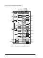

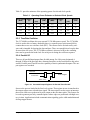
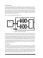
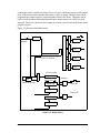

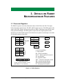
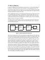
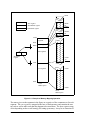
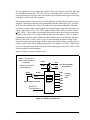
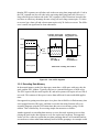

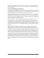

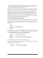
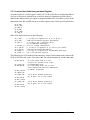
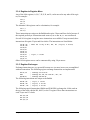
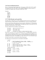
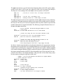
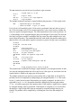
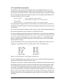

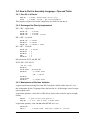
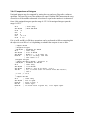
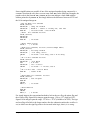
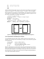
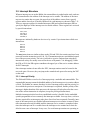
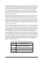
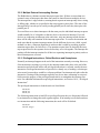

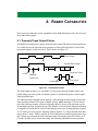

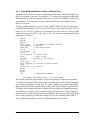
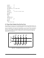

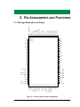
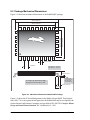
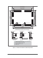
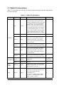
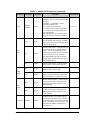
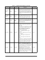
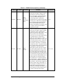


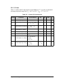
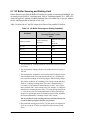


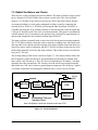
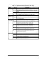
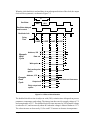

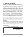
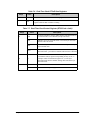
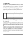
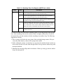
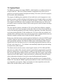

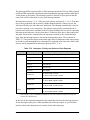
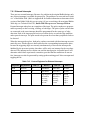


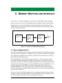
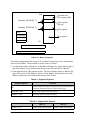
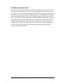
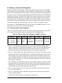

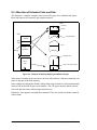
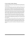
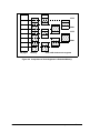
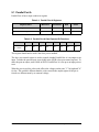
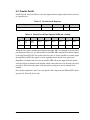
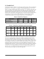


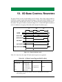
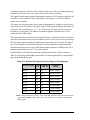


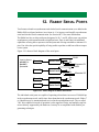
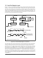
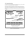

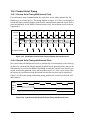

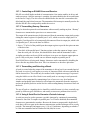
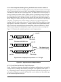
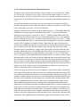
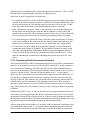

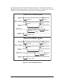
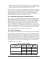
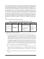
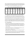
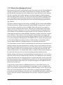
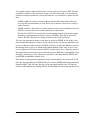

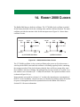

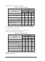
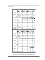
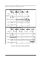
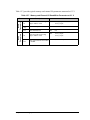


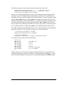


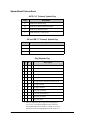

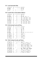
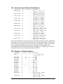

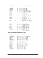
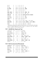
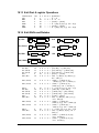
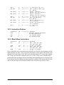
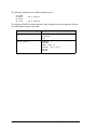

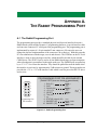


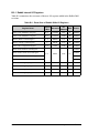
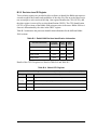


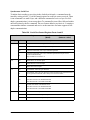
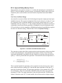
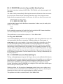
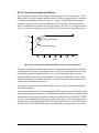
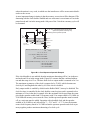


![FICON_AdminGd_v700[1].](http://vs1.manualzilla.com/store/data/005962703_1-207ddf39f2a91b852624dcbb8fd7d57f-150x150.png)