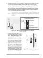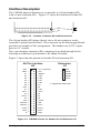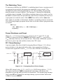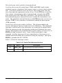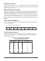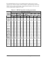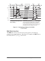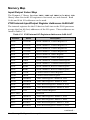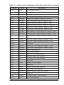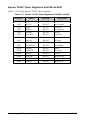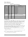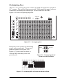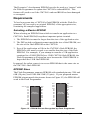
1
CM7000 Series C-Programmable Core Module Users Manual Revision F CM7000 Series Core Modules Users Manual Part Number 019-0018 Revision F Last revised on February 18, 1999 Printed in U.S.A. Copyright © 1999 Z-World All rights reserved. Z-World reserves the right to make changes and improvements to its products without providing notice. Trademarks Dynamic C® is a registered trademark of Z-World Windows® is a registered trademark of Microsoft Corporation PLCBus is a trademark of Z-World Hayes Smart Modem® is a registered trademark of Hayes icrocomputer Products, Inc. Notice to Users When a system failure may cause serious consequences, protecting life and property against such consequences with a backup system or safety device is essential. The buyer agrees that protection against consequences resulting from system failure is the buyers responsibility. This device is not approved for life-support or medical systems. All Z-World products are 100 percent functionally tested. Additional testing may include visual quality control inspections or mechanical defects analyzer inspections. Specifications are based on characterization of tested sample units rather than testing over temperature and voltage of each unit. Z-World may qualify components to operate within a range of parameters that is different than the manufacturers recommended range. This strategy is believed to be more economical and effective. Additional testing or burn-in of an individual unit is available by special arrangement. Company Address Z-World 2900 Spafford Street Davis, California 95616-6800 USA Telephone: Facsimile: Web Site: E-Mail: (530) 757-3737 (530) 753-5141 http://www.z w orld.c om [email protected] TABLE OF CONTENTS About This Manual ix Chapter 1: Overview 13 Chapter 2: Getting Started 19 Chapter 3: System Development 33 Introduction .......................................................................................... 14 Features ........................................................................................... 14 Options ................................................................................................. 14 CM7100 Series ............................................................................... 14 CM7200 Series ............................................................................... 16 Software Development and Evaluation Tools ...................................... 17 Programming Setup ............................................................................. 20 CM7100 ............................................................................................... 20 CM7100 Method 1 Prototyping Board ...................................... 21 CM7100 Method 2 Development Board .................................... 24 CM7100 Method 3 Embedded in System .................................. 27 CM7100 Method 4 In-Target Direct Development .................... 28 Safeguards .................................................................................... 29 CM7200 ............................................................................................... 30 CM7200 Method 1 Prototyping Board ...................................... 30 CM7200 Method 2 Embedded In System .................................. 32 General Description ............................................................................. 34 Interface Description ............................................................................ 36 CM7000 Subsystems ........................................................................... 39 DMA ............................................................................................... 39 DMA Registers ............................................................................. 40 Software ........................................................................................ 41 Programmable Timers ..................................................................... 42 Software ........................................................................................ 42 EPROM ........................................................................................... 43 CM7100 ........................................................................................ 43 CM7200 ........................................................................................ 45 SRAM ............................................................................................. 46 EEPROM ........................................................................................ 47 Real-Time Clock (RTC) .................................................................. 47 CM7000 Table of Contents s iii Power Management ......................................................................... 48 Handling Power Fluctuations ........................................................ 49 The Watchdog Timer .................................................................... 52 Power Shutdown and Reset .......................................................... 52 PFI Early Warning ..................................................................... 52 Memory Protection ....................................................................... 53 Battery/Super Capacitor Backup .................................................. 53 System Reset ................................................................................... 55 Serial Communication .......................................................................... 56 RS-232 Communication .................................................................. 57 Receive and Transmit Buffers ....................................................... 58 Echo Option .................................................................................. 58 CTS/RTS Control ......................................................................... 58 XMODEM File Transfer ................................................................. 58 Modem Communication .................................................................. 59 Interrupt Handling for Z180 Port 0 ............................................... 59 Software Support .......................................................................... 60 Master-Slave Networking ............................................................... 60 Software Support .......................................................................... 61 Use of the Serial Ports ..................................................................... 62 Attainable Baud Rates .................................................................. 63 Z180 Serial Ports .......................................................................... 63 Asynchronous Serial Communication Interface ................................... 65 ASCI Status Registers ..................................................................... 65 /DCD0 (Data Carrier Detect) ........................................................ 65 TIE (Transmitter Interrupt Enable) ............................................... 65 TDRE (Transmitter Data Register Empty) ................................... 65 CTS1E (CTS Enable, Channel 1) ................................................. 66 RIE (Receiver Interrupt Enable) ................................................... 66 FE (Framing Error) ....................................................................... 66 PE (Parity Error) ........................................................................... 66 OVRN (Overrun Error) ................................................................ 66 RDRF (Receiver Data Register Full) ............................................ 66 ASCI Control Register A ................................................................ 67 MOD0MOD2 (Data Format Mode Bits) .................................... 67 MPBR/EFR (Multiprocessor Bit Receive/Error Flag Reset) ........ 67 /RTS0 (Request to Send, Channel 0) ............................................ 67 CKA1D (CKA1 Disable) .............................................................. 67 TE (Transmitter Enable) ............................................................... 67 RE (Receiver Enable) ................................................................... 68 MPE (Multiprocessor Enable) ...................................................... 68 iv s Table of Contents CM7000 ASCI Control Register B ................................................................ 68 SS (Source/Speed Select) ............................................................. 68 DR (Divide Ratio) ........................................................................ 69 PEO (Parity Even/Odd) ................................................................ 69 /CTS/PS (Clear to Send/Prescaler) ............................................... 69 MP (Multiprocessor Mode) .......................................................... 69 MPBT (Multiprocessor Bit Transmit) .......................................... 69 Chapter 4: Design Considerations 71 Appendix A: Troubleshooting 81 Appendix B: Specifications 85 Appendix C: Memory, I/O Map, and Interrupt Vectors 91 Bus Loading ......................................................................................... 72 Bus Timing ........................................................................................... 76 Standard I/O Cycles ............................................................................. 76 Wait State Insertion ......................................................................... 77 System Power ....................................................................................... 78 Power-On and Reset Management ....................................................... 79 Watchdog Timer ................................................................................... 79 I/O Addressing ..................................................................................... 80 Out of the Box ...................................................................................... 82 Dynamic C Will Not Start .................................................................... 83 Dynamic C Loses Serial Link .............................................................. 83 CM7000 Repeatedly Resets ................................................................. 83 Common Programming Errors ............................................................. 84 Electrical and Mechanical Specifications ............................................ 86 Mechanical Dimensions .................................................................. 87 Jumpers and Headers ........................................................................... 88 CM7100 .......................................................................................... 88 CM7200 .......................................................................................... 89 CM7000 Memory ................................................................................ 92 Execution Timing ............................................................................ 93 Memory Map ....................................................................................... 94 Input/Output Select Map ................................................................. 94 Z180 Internal Input/Output Register Addresses 0x00-0x3F ........... 94 Epson 72423 Timer Registers 0x41800x418F .............................. 96 Other Addresses .............................................................................. 97 I/O Addressing .............................................................................. 97 CM7000 Table of Contents s v Interrupt Vectors .................................................................................. 98 Nonmaskable Interrupts .................................................................. 99 INT0 ................................................................................................ 99 INT1 ................................................................................................ 99 INT2 ................................................................................................ 99 Jump Vectors ................................................................................. 100 Interrupt Priorities ......................................................................... 100 Appendix D: EEPROM 101 Appendix E: Serial Interface Board 2 105 Appendix F: Prototyping Board 109 Appendix G: Development Board 121 Appendix H: LCD/Keypad Module 125 Appendix I: Flash Programmer 131 Library Routines ................................................................................ 103 Introduction ........................................................................................ 106 External Dimensions .......................................................................... 107 Description ......................................................................................... 110 Interfaces ....................................................................................... 111 Power ............................................................................................ 112 Prototyping Area ........................................................................... 113 Reset .............................................................................................. 114 Dimensions ........................................................................................ 115 Jumpers and Headers ......................................................................... 116 Sample Circuits .................................................................................. 119 Digital Input .................................................................................. 119 Digital Output ............................................................................... 120 The LCD Driver ................................................................................. 128 The Keypad Driver ............................................................................ 129 Introduction ........................................................................................ 132 Nonremovable Flash EPROM ...................................................... 132 Requirements ..................................................................................... 133 Selecting a Master EPROM .......................................................... 133 EPROM Sizes ............................................................................... 133 Back-Panel DIP switches .............................................................. 134 vi s Table of Contents CM7000 Operating Procedure to Copy Application ......................................... 135 BIOS Update/Recovery Mode ........................................................... 136 Troubleshooting ................................................................................. 137 CM7100 Compatibility ...................................................................... 137 Appendix J: Sample Applications 139 Appendix K: Sample Programs 153 Index 157 CM7000 Table of Contents s vii 12-Bit Analog-to-Digital Converter ................................................... 140 Optically Isolated Switch Reader ....................................................... 143 Relay Circuit ...................................................................................... 144 24-Bit Parallel I/O .............................................................................. 146 8-Bit Digital-to-Analog Converter ..................................................... 147 SRAM Interface ................................................................................. 149 Protection Circuits ............................................................................. 150 Digital-Noise Filter ....................................................................... 150 Serial-Port Protection .................................................................... 150 Digital I/O Protection .................................................................... 151 Suppliers of Board-Level Protection Devices ............................... 151 Sample Programs on Special EPROM ............................................... 154 Other Sample Programs ..................................................................... 156 Blank viii s Table of Contents CM7000 ABOUT THIS MANUAL This manual describes the CM7000 Series core modules, their subsystems, and the CM7100 Evaluation Kit. For ease of reference, this manual uses CM7000 as a generic term referring to any of the CM7100 or CM7200 Series modules. CM7100 refers to any of the CM7100 Series modules, and CM7200 refers to the CM7200 Series. Specific models are referenced when appropriate. Instructions are also provided for using Dynamic C functions. Assumptions Assumptions are made regarding the user's knowledge and experience in the following areas: Ability to design and engineer a target system that uses a CM7000. Understanding of the basics of operating a software program and editing files under Windows on a PC. Knowledge of the basics of C programming. $ For a full treatment of C, refer to the following texts: The C Programming Language by Kernighan and Ritchie C: A Reference Manual by Harbison and Steel Knowledge of basic Z80 assembly language and architecture. $ For documentation from Zilog, refer to the following texts: Z180 MPU User's Manual Z180 Serial Communication Controllers Z80 Microprocessor Family User's Manual CM7000 About This Manual s ix Acronyms Table 1 is a list of acronyms that may be used in this manual. Table 1. Acronyms Acronym Meaning EPROM Erasable Programmable Read Only Memory EEPROM Electronically Erasable Programmable Read Only Memory LCD Liquid Crystal Display LED Light Emitting Diode NMI Nonmaskable Interrupt PIO Parallel Input / Output Circuit (Individually Programmable Input / Output) PRT Programmable Reload Timer RAM Random Access Memory RTC Real Time Clock SIB Serial Interface Board SRAM Static Random Access Memory UART Universal Asynchronous Receiver Transmitter Icons Table 2 displays and defines icons that may be used in this manual. Table 2. Icons Icon $ ( Meaning Refer to or see ! Please contact Caution )' Icon Meaning Note High Voltage 7LS Tip Factory Default x s About This Manual CM7000 Conventions Table 3 lists and defines typographical conventions that may be used in this manual. Table 3. Typographical Conventions Example Description while Courier font (bold) indicates a program, a fragment of a program, or a Dynamic C keyword or phrase. // IN-01… Program comments are written in Courier font, plain face. Italics Indicates that something should be typed instead of the italicized words (e.g., in place of filename, type a file’s name). Edit Sans serif font (bold) signifies a menu or menu selection. ... An ellipsis indicates that (1) irrelevant program text is omitted for brevity or that (2) preceding program text may be repeated indefinitely. [ ] Brackets in a C function’s definition or program segment indicate that the enclosed directive is optional. ‹ › Angle brackets occasionally enclose classes of terms. a | b | c A vertical bar indicates that a choice should be made from among the items listed. A black square indicates pin 1 of all headers. Pin 1 J1 Pin Number 1 Measurements All diagram and graphic measurements are in inches followed by millimeters enclosed in parenthesis. CM7000 About This Manual s xi Blank xii s About This Manual CM7000 CHAPTER 1: CM7000 OVERVIEW Overview s 13 Introduction The CM7000 is a microprocessor core module. The CM7000 combines a complete system engine with integrated development software. You build your own controller around the plug-in CM7000. Features Small size: 1.80" × 2.05" (45.7 mm × 52.1 mm) Microprocessor: Z180 running at 9.216 MHz or 18.432 MHz, including two DMA channels, two serial ports, and two programmable timers (PRTs ) SRAM: 32K or 128K (512K factory-installed SRAM is also available) EPROM: CM710032-pin DIP socket accommodates up to 512K EPROM CM7200128K flash EPROM at 128 bytes/sector (256K factoryinstalled flash EPROM is also available) I/O support: six chip-select lines, supporting 64 addresses each, control the applications hardware Low electromagnetic interference Software written for either CM7100 or CM7200 Series is binarycompatible with the other Options The CM7000 is available with two types of memoryCM7100s have ROM and CM7200s have flash EPROM. CM7100 Series Table 1-1 lists the features of each model in the CM7100 Series. Table 1-1. CM7100 Series Features Model Features CM7100 18.432 MHz clock, 128K SRAM, 512-byte EEPROM, real-time clock, and ADM691 supervisor CM7110 CM7100 with 9.216 MHz clock CM7120 CM7100 with 9.216 MHz clock and 32K SRAM CM7130 CM7100 with 9.216 MHz clock and 32K SRAM. Without ADM691 supervisor, real-time clock and EEPROM. 14 s Overview CM7000 The CM7100 is available in one of the models listed in Table 1-1 or as part of the Evaluation Kit. The Evaluation Kit contains the following items. CM7110 with special EPROM containing sample programs. Prototyping Board. Manual (with schematics), cables, AC adapter, trial version of Dynamic C development software. The trial version of Dynamic C included with the Evaluation Kit contains only the libraries associated with the Evaluation Kit. Once a decision is made to proceed with normal development, the standard or deluxe version of Dynamic C must be purchased. The Development Board supplied with the Developers Kit and the development EPROM are also available for separate purchase. ( For help with upgrading to a full-scale system, call your Z-World Sales Representative at (530) 757-3737. A Developers Kit is available for the CM7100. The Developers Kit contains the following items. Development EPROM. Development Board, which plugs into the CM7100 EPROM socket to emulate ROM with RAM to make it easier to develop and debug large programs. Manual (with schematics), cables, and AC adapter. A 128K EPROM and an LCD/Keypad module (the LCD/Keypad module requires a 9.216 MHz clock) are available separately. Figure 1-1 shows the CM7100 board layout. J3 U6 U4 PAL U2 RAM RTC J1 U8 (R1) Sel. U5 U7 U3 U1 (H3) Y1 J2 EPROM Z180 691 H2 H1 Top Side Microprocessor Side Figure 1-1. CM7100 Board Layout CM7000 Overview s 15 CM7200 Series Table 1-2 lists the features of each model in the CM7200 Series. Table 1-2. CM7200 Series Features Model Features CM7200 18.432 MHz clock, 128K SRAM, real-time clock, ADM691 supervisor, and 128K flash EPROM CM7210 CM7200 with 9.216 MHz clock CM7220 CM7200 with 9.216 MHz clock and 32K SRAM CM7230 CM7200 with 9.216 MHz clock and 32K SRAM. Without ADM691 supervisor and real-time clock. A Developers Kit is available for the CM7200. The Developers Kit contains the following items. Prototyping Board. Manual (with schematics), cables and AC adapter. Serial Interface Board 2. The following optional accessories are available for the CM7200. Flash Programmer to program flash EPROM. 256K factory-installed flash EPROM. LCD/Keypad module (2 × 20 LCD and 2 × 6 keypad) for use with CM7200 modules with a 9.216 MHz clock. Figure 1-2 shows the CM7200 board layout. U5 Y1 U2 RAM U1 RTC 691 U8 Z180 U3 Flash EPROM JP1 U7 PAL H2 H1 Top Side U6 H2 H1 Microprocessor Side Figure 1-2. CM7200 Board Layout 16 s Overview CM7000 Software Development and Evaluation Tools Dynamic C, Z-Worlds Windows-based real-time C language development system, is used to develop software for the CM7000. The host PC downloads the executable code through the CM7000s RS-232 serial port or through the Serial Interface Board 2 to one of the following places: battery-backed RAM, ROM written on a separate EPROM programmer and then substituted for the Z-World development EPROM, or flash EPROM. Dynamic C allows fast in-target development and debugging. $ ( CM7000 Z-Worlds Dynamic C reference manuals provide complete software descriptions and programming instructions. For ordering information or more details about the various options and prices, call your Z-World Sales Representative at (530) 757-3737. Overview s 17 Blank 18 s Overview CM7000 CHAPTER 2: CM7000 GETTING STARTED Getting Started s 19 Programming Setup Dynamic C, Z-Worlds C-language development system, is used to develop applications for the CM7000. As a program compiles, Dynamic C downloads it directly to the CM7000s memory via one of the PC COM ports. Serial communication is normally at 19,200 bps, and can be as high as 57,600 bps. The CM7000 remains connected to the PC in most instances while a program is undergoing development. The mechanics of connecting a CM7000 and a PC vary depending on the CM7000 version and the programming strategy. The programming strategy for a CM7100 depends on the hardware setup. Only one programming method is available for the CM7200 regardless of whether the Developers Kit or in-target development is used. CM7100 Four methods are available to program the CM7100. 1. Using the Prototyping Board. This method is recommended for programming the CM7110 supplied in the Evaluation Kit. This CM7110 has a special EPROM that contains the BIOS and sample programs. Method 1 may also be used to program other CM7100s. Since an EPROM is not normally included with CM7100s, except for the CM7110 in the Evaluation Kit, which comes with a special EPROM, a custom EPROM with the contents of the Dynamic C 2903.BIN file must first be burned according to the details in the section Programming EPROMs in Chapter 3, System Development. 2. Using the Development Board. The Development Board is included in the Developers Kit with full Dynamic C, and is also sold separately. 3. Using the Development Board with full Dynamic C, and with the CM7100 embedded in your target system. 4. Directly in your system without a Development Board. This method requires some hardware setup and minor modifications to the Dynamic C EPROM code. Methods 1 and 2 are normally used for evaluation or experimentation. Method 3 requires some hardware setup, and ultimately must be used to program a working system. Method 4 can be the fastest and most powerful. Once program development has been completed, recompile the program for EPROM. An EPROM is burned in a separate operation and is then installed in the EPROM socket on the CM7100. 20 s Getting Started CM7000 CM7100 Method 1 Prototyping Board 1. Check to make sure the power to the Prototyping Board is not connected. 2. Check header J3 on the microprocessor side of the CM7100. The surface-mounted jumper should connect pins 23 to reflect the 128K memory of the special EPROM. This factory default setting is shown in Figure 2-1. 1 2 3 J3 FD J3 U6 Y1 J2 PAL J1 Figure 2-1. CM7100 Header J3 Configured for Special EPROM 3. Plug the CM7100 into the Prototyping Board as shown in Figure 2-2. Plug header H2 of the CM7100 into connector H3 of the Prototyping Board. Pins 1 of the header and connector must match. The CM7100 will hang over the battery on the Prototyping Board. For maximum stability, install the supplied standoff between the CM7100 and the Prototyping Board. Special EPROM (680-295x) CM7100 H2 Standoff Power Jack H3 Battery Prototyping Board Figure 2-2. Connecting CM7100 to Prototyping Board 4. If using the CM7110 from the Evaluation Kit, make sure the CM7110 has the special 32-pin EPROM (Z-World part number 680-295x) installed at U3 as shown in Figure 2-3. Custom-burned EPROM are also installed at location U3. U4 RAM U3 32-pin EPROM Figure 2-3. Installation of 32-pin EPROM CM7000 Getting Started s 21 5. Place jumpers across headers J2, J3, and J4 on the Prototyping Board to enable headers J6J11 on the Prototyping Board. The Prototyping Board is shown in Figure 2-4. Power Jack J1 SmartCore Evaluation Board H1 Reset Buzzer H2 Configuration Jumpers Programming Port J2 J3 J4 RP1 H4 CM7000 connector H3 CM7000 location Serial Port Battery H5 J5 SW2 LED2 SW3 LED3 SW4 LED4 SW5 LED5 J6 J7 J8 J9 J10 J11 Figure 2-4. CM7100 Prototyping Board ! It is necessary to place jumpers across headers J2, J3, and J4 to enable headers J6J11 on the Prototyping Board. Note that this disables chip selects CS1, CS2, and CS3. The LEDs will not work when CS1 is disabled. ! The BIOS on the special EPROM (Z-World part number 680-295x) supplied with the CM7110 in the Evaluation Kit does not support chip selects CS1, CS2, and CS3. 22 s Getting Started CM7000 6. Set the Prototyping Boards jumpers. Jumpers across headers J10 and J11 affect the operational mode and the baud rate as shown in Figure 2-5. When both headers J10 and J11 are jumpered, the CM7100 checks headers J6J9 at startup. If none of these headers is jumpered, the CM7100 will execute the program, if any, stored in RAM. If some of these headers are jumpered, a sample program stored in the special CM7100 EPROM will begin executing. $ See Appendix F, Prototyping Board, for more information on the Prototyping Board and the sample programs in the special EPROM. Prototyping Board Jumper Settings Program/Baud Rate FD J6 J7 J8 J9 J10 J11 Baud Rate J10 J11 19,200 bps J10 J11 9600 bps J10 J11 57,600 bps J10 J11 Run program in RAM or special EPROM Figure 2-5. CM7100 Prototyping Board Program/Mode Jumper Settings 8. Apply power from the 9 V power supply to the Prototyping Board. The CM7100 is ready for programming, unless the jumpers were set in Step 6 to run a program stored in RAM or to run one of the sample programs stored in the special EPROM. CM7000 Serial cable to PC Program H4 H5 Serial 7. Connect the serial cable. Connect one end to the PC COM port. Then connect the 10-pin end to header H4 of the Prototyping Board as shown in Figure 2-6. Be careful to match the arrow on the connector to the location of pin 1 on header H4. Figure 2-6. Serial Cable Connection to CM7100 Prototyping Board Getting Started s 23 CM7100 Method 2 Development Board 1. Check to make sure the power to the Prototyping Board is not connected. 2. Check header J3 on the microprocessor side of the CM7100. The surface-mounted jumper should connect pins 23 to use the Development Board. This factory default setting is shown in Figure 2-1. 3. Plug the CM7100 into the Prototyping Board as shown in Figure 2-7. Plug header H2 of the CM7100 into connector H3 of the Prototyping Board. Pins 1 of the header and connector must match. The CM7100 will hang over the battery on the Prototyping Board. For maximum stability, install the supplied standoff between the CM7100 and the Prototyping Board. CM7100 H2 Standoff H3 Battery Power Jack Prototyping Board Figure 2-7. Connecting CM7100 to Prototyping Board 4. If an EPROM is installed in socket U3 on the CM7100, remove the EPROM. Plug a Dynamic C development EPROM (Z-World part number 680-290x) into the EPROM socket (U3) of the Development Board. See Figure 2-8. U3 Development Board H2 Dynamic C EPROM (680-290x) U6 U3 CM7100 Figure 2-8. Installation of CM7100 Development Board and Development EPROM 24 s Getting Started CM7000 5. Plug the Development Board into the EPROM (U3) and H3 sockets on the CM7100 as shown in Figure 2-8. Headers U6 and H2 on the underside of the Development Board must match the CM7100 EPROM and H3 sockets exactly. Be careful! The U6 and H2 pins on the Development Board are delicate and bend easily. 6. Check the jumpers on the Development Board. Figure 2-9 shows the locations of the relevant headers. U3 Battery EPROM (U1) U2 Super. UART RS-232 JP1 Y1 U5 H1 (H2) U4 RAM U7 U8 PAL RS-232 JP2 JP3 JP4 Buffer JP5 Figure 2-9. CM7100 Development Board Figure 2-10 shows the jumper settings for different RAM sizes, operational modes, and baud rates. Development Board RAM Jumper Settings JP1 32K, 128K RAM FD 512K RAM JP1 Development Board Jumper Settings Program/Baud Rate FD JP3 JP4 19,200 bps JP3 JP4 9600 bps JP3 JP4 57,600 bps JP3 JP4 Run program in Development Board RAM Figure 2-10. CM7100 Development Board Jumper Settings CM7000 Getting Started s 25 JP1 7. If you are using a 28-pin RAM chip, seat the chip in the RAM socket as shown in Figure 2-11. U5 RAM Figure 2-11. Position of 28-Pin Chip in 32-Pin Socket Serial cable to PC H1 JP2 JP3 JP4 Figure 2-12. Serial Cable Connection to CM7100 Development Board 8. Connect the serial cable. Connect one end to the PC COM port. Then connect the 10-pin end to H1 of the Development Board as shown in Figure 2-12. Be careful to match the arrow on the connector to the location of pin 1 on header H1. 9. Reconnect the 9 V power supply to the Prototyping Board. The CM7100 is ready for programming, unless the jumpers were set in Step 5 to run a program in the Development Boards RAM. 26 s Getting Started CM7000 CM7100 Method 3 Embedded in System Method 3 assumes that the CM7100 is already mounted in a system and that the CM7100 is properly connected. At a minimum, regulated power (+5 V) and ground must be provided. The Development Board plugs into the EPROM socket of the CM7100. The Development Board emulates the system EPROM normally installed in the CM7100, providing up to 504K of program space in addition to the RAM on the CM7100 (used as a data space). The Development Board has its own RS-232 port and communicates directly with the PC during program development. 1. Disconnect power from the CM7100. 2. If an EPROM is installed in socket U3 on the CM7100, remove the EPROM. Plug a Dynamic C development EPROM (Z-World part number 680-290x) into the EPROM socket (U3) of the Development Board. See Figure 2-8. 3. Plug the Development Board into the EPROM (U3) and H3 sockets on the CM7100 as shown in Figure 2-8. Headers U6 and H2 on the underside of the Development Board must match the CM7100 EPROM and H3 sockets exactly. Be careful! The U6 and H2 pins on the Development Board are delicate and bend easily. 4. Check header J3 on the microprocessor side of the CM7100. The surface-mounted jumper should connect pins 23 to use the Development Board. This factory default setting is shown in Figure 2-1. 5. Check the jumpers on the Development Board. Figure 2-9 shows the locations of the relevant headers. Figure 2-10 shows the jumper settings for different RAM sizes, and for the operational mode and baud rates. 6. If you are using a 28-pin RAM chip, seat the chip in the RAM socket as shown in Figure 2-11. 7. Connect the serial cable. Connect one end to the PC COM port. Then connect the 10-pin end to H1 of the Development Board as shown in Figure 2-12. Be careful to match the arrow on the connector to the location of pin 1 of H1. 8. Reconnect power to the CM7100. The CM7100 is ready for programming, unless the jumpers were set in Step 5 to run a program stored in the Development Board RAM. CM7000 Getting Started s 27 CM7100 Method 4 In-Target Direct Development It is possible to program directly through a CM7100s built-in serial port without using a Development Board. In this method, the program is held in RAM while the application is under development. At least 128K of RAM is highly recommended. Note that the CTS0 input must be asserted for channel z0 to transmit. Tie CTS0 to ground if RTS/CTS handshake support is not needed. 1. Build an input port into your hardware using one of the /CS lines. One bit of the input will specify whether the Dynamic C monitor in the EPROM enters RUN mode or PROGRAM mode. 2. Build a serial driver into your system based on the one on the Prototyping Board (see Figure 2-13). H4 MAX232 TXA1 RXA1 Z180 4.7 µF CM7100 4.7 µF TX1 /TX1 RX1 /RX1 10 kΩ /TX1 /RX1 C1+ C1– C2+ C2– 4.7 µF V+ V– 4.7 µF Figure 2-13. CM7100 Prototyping Board Serial Driver If your serial driver has a 10-pin header that conforms to Z-Worlds programming cable, you will not need to build another programming cable. CTS and RTS are tied together and pulled up. 3. Six bytes of the Dynamic C EPROM (starting at 0x70 in the EPROM file) are reserved as indicated in Table 2-1. Table 2-1. Dynamic C EPROM Addresses Address Name Range 0x70 channel 0,1 0x71 baud rate 0x72,73 address 0x74 mask 0x75 polarity 28 s Getting Started Meaning Selects serial programming port. 1–48 Programming baud rate in multiples of 1200 bps: 8 = 9600 bps, 16 = 19,200 bps, 48 = 57,600 bps). 0x4000 to 0x417F Address of input port (corresponds to /CS line), low-order bits in byte 72. 0x0–FF 0,1 Active bit(s) of input byte, one bit suffices. Polarity of input bit. CM7000 Modify the Dynamic C EPROM file (in your Dynamic C directory) and burn a new EPROM with the appropriate new data. When a system resets, the Dynamic C monitor in the EPROM consults the 6 bytes. If the monitor finds valid data, the system will start operating according to the data. The monitor will attempt to read the specified input port. If it is successful, the monitor will either enter programming mode (communicating with Dynamic C in a PC) or run the program stored in the CM7100s RAM. For example, the C structure (70) (71) (72,73) (74) (75) 0x00 0x10 0x4040 0x80 0x00 serial channel 0 19,200 bps /CS2 active bit is bit 7 active bit = 0 ® PROGRAM mode else RUN mode would work and might use an input port such as the one shown in Figure 2-14. +5 V /CS2 1 /RD 18 74HC32 D7 10 kΩ /OE Y0 A0 2 74HC244 Jumper: Connected for PROGRAM mode Open for RUN mode Figure 2-14. Input Port With the standard CM7100 BIOS (2903 or later), setting the I/O address (bytes 0x72 and 0x73) to 0x0000 will force the CM7100 into development mode. This setting eliminates the need to use a RUN/ PROGRAM jumper. Direct development is not supported by the BIOS of the CM7110 included in the CM7100 Evaluation Kit. Safeguards The following safeguards have been adopted. 1. If there is no valid program in RAM, the Dynamic C monitor will repeatedly go into a tight loop, forcing a watchdog timeout. 2. If byte 0x70 is not a 0 or 1, the monitor is forced to RUN mode. 3. If byte 0x71 is not a multiple of 8, the monitor is forced to RUN mode. 4. If bytes 0x72 and 0x73 have an address less than 0x4000 or greater than 0x417F, the monitor is forced to RUN mode. The Dynamic C development EPROM has the six locations all set to 0xFF. CM7000 Getting Started s 29 CM7200 The CM7200 uses its Z180 microprocessors CSI/O (clocked serial I/O) line for communicating with Dynamic C running on a host PC; Z-Worlds SIB22 makes the CSI/O port look just like an RS-232 port. Since the CM7200s flash EPROM is electrically reprogrammable in a circuit, the flash EPROM requires no ROM emulation during development. Consequently the CM7200s programming strategy is very simple when compared to the CM7100s. CM7200 Method 1 Prototyping Board 1. Check to make sure the power to the Prototyping Board is not connected. 2. Plug the CM7200 into the Prototyping Board as shown in Figure 2-15. Plug header H2 of the CM7200 into connector H3 of the Prototyping Board. Pins 1 of the header and connector must match. The CM7200 will extend over the battery on the Prototyping Board. For maximum stability, install the supplied standoff between the CM7200 and the Prototyping Board. JP1 (to SIB2) CM7200 H2 Standoff Battery H3 Power Jack Prototyping Board Figure 2-15. Connecting CM7200 to Prototyping Board 3. Connect the 6-conductor RJ-12 cable provided with the Developers Kit from the PC serial-port adapter to the SIB2 as shown in Figure 216. Connect the 2 mm ribbon cable from the SIB2 to header JP1 on the CM7200. Be careful to match the arrow on the connector to Pin 1 of JP1. 4. Set the baud rate of the host PCs COM port to 9600 bps, 19,200 bps, or 57,600 bps. 5. Apply power to the Prototyping Board. As a minimum, the power supply must have regulated +5 V and GND for the CM7200. The CM7200 is now ready for programming. 30 s Getting Started CM7000 To PC COM Port 6-conductor, RJ-12 Cable 6-pin RJ-12 Male RJ-12 to DB-9 Adapter 6-pin RJ-12 Male Marked Conductor to Pin 1 CM7200 Core module Pin 1 JP1 Figure 2-16. CM7200 Connection to Serial Interface Board 2 CM7000 Getting Started s 31 CM7200 Method 2 Embedded In System 1. Disconnect power from the system. 2. Connect the 6-conductor RJ-12 cable provided in the Developers Kit from the PCs serial-port adapter to the SIB2. 3. Connect the 2 mm ribbon cable from the SIB2 to header JP1 on the CM7200. Be careful to match the arrow on the connector to Pin 1 of JP1. 4. Set the baud rate of the host PCs COM port to 9600 bps, 19,200 bps, or 57,600 bps. 5. Reconnect power to the system. As a minimum, the power supply must have regulated +5 V and GND for the CM7200. The system is now ready for programming. 32 s Getting Started CM7000 CHAPTER 3: CM7000 SYSTEM DEVELOPMENT System Development s 33 General Description The CM7000 is a complete system engine that contains the microprocessor and memory around which a controller is built. Figure 3-1 shows a block diagram of the CM7100. A6–A8 EEPROM Z180 DMA Request DMA End Interrupt (2) PRTs (2) Serial Ports (2) DMA Channels MMU A0–A19 VBAT /CS1–/CS6 A0–A5 D0–D7 SRAM EPROM 32K–512K 32K–512K +5 V GND VRAM Supervisor Watchdog Timer Power Failure Warning Reset Control Battery Backup Control Decoder RTC CS VRAM Figure 3-1. CM7100 Block Diagram Figure 3-2 shows a block diagram of the CM7200. A6–A8 Clocked Serial I/O DMA Request DMA End Interrupt Z180 (2) PRTs (2) Serial Ports (2) DMA Channels MMU A0–A19 VBAT /CS1–/CS6 A0–A5 D0–D7 SRAM Flash Memory 32K–512K 128K–256K +5 V GND VRAM Supervisor Watchdog Timer Power Failure Warning Reset Control Battery Backup Control Decoder RTC CS VRAM Figure 3-2. CM7200 Block Diagram The microprocessor is a Z180, running at either 9.216 MHz or 18.432 MHz. The Z180 has two asynchronous serial ports, two DMA channels, and two programmable-reload timers (PRTs). Two of the Z180s interrupt lines are available for use in the system. 34 s System Development CM7000 The Z180 supports a 1M address space with its internal memory management unit (MMU). It has 20 address lines. The data path is 8 bits wide lines D0D7. Six chip-select lines (/CS1/CS6) enable one of six groups of 64 input/ output addresses. Thus, single-tier addressing can directly access 384 distinct devices or registers. The optional power-supervisor IC, an ADM691, provides several services. It has a watchdog timer, performs power-failure detection, and supports battery backup. When power fails, it protects the RAM from being accidentally overwritten. Your application can obtain the time and the date from the optional realtime clock IC, an Epson 72423. The optional CM7100 EEPROM (24C04) stores 512 bytes of nonvolatile data for system constants and other important values. The upper 256 bytes of the EEPROM can be write-protected by breaking a circuit board trace. The CM7200 simulates the EEPROM in its flash memory. This simulation is software-compatible with the CM7100s Dynamic C EEPROM function calls. $ CM7000 See Appendix D, EEPROM, for more information on the software function calls and details about write-protecting the CM7100 EEPROM. System Development s 35 Interface Description The CM7000 physical interface to a controller is a 40-pin header (H2) with a 5-pin extension (H1). Figure 3-3 shows the location of header H2 and extension H1. H2 H1 Figure 3-3. Location of Header H2 and Extension H1 The 40-pin header (H2) plugs directly into a 40-pin connector on the controllers printed circuit board. The connector on the Prototyping Board provides an example of this arrangement. The headers use 0.025" square pins on 0.1" centers. The 5-pin interface extension (H1) comprises five plated through-holes, allowing an additional 5-pin header to be added if needed. Figure 3-4 provides the pinouts for header H2 and extension H1. Extension H1 40-Pin Interface H2 GND VBAT D1 D2 1 2 +5 V (regulated) 3 4 5 6 7 8 / PFI / RESET /CS5 D3 D4 D5 D6 /CS4 9 10 11 12 13 14 15 16 17 18 A1 /INT1 19 20 21 22 A3 /WAIT D7 /WR /DREQ0 23 24 25 26 27 28 29 30 31 32 /DREQ1 /CTS0 TXA0 E 33 34 35 36 37 38 39 40 /CS6 /CS1 /CS2 D0 A0 1 GND 2 VRAM /TEND0 3 4 5 /TEND1 /RTS0 / signals are active low /CS3 / INT0 A2 A4 A5 / IORQ / RD TXA1 RXA0 RXA1 GND Figure 3-4. CM7000 Pinouts for Header H2 and Extension H1 36 s System Development CM7000 Table 3-1 lists the CM7000 interface signals. Table 3-1. CM7000 Interface Signals Signal Name Direction Description A0–A5 Out Address lines. CMOS compatible. D0–D7 Bi. Data lines. TTL/CMOS compatible. /RD Out Read. Defines a read cycle. Directly connected to Z180. TTL/CMOS compatible. /WR Out Write. Defines a write cycle. Directly connected to Z180. TTL/CMOS compatible. /INT0 In Maskable interrupt request 0. TTL/CMOS compatible. /INT1 In Maskable interrupt request 1. TTL/CMOS compatible. /IORQ Out I/O Request. Defines an I/O cycle. Directly connected to Z180. TTL/CMOS compatible. /CS1– /CS6 Out Chip selects (6). Each selects a group of 64 I/O addresses. TTL/CMOS compatible /WAIT In Wait line. Generates wait states for I/O cycles. Allows access to slow I/O devices. Directly connected to Z180. TTL/CMOS compatible. /DREQ0, /DREQ1 In DMA request lines. Requests movement of one byte of data on specified DMA channel (0 or 1). Can be edgeor level-sensitive. Ignored during memory-to-memory and serial-to-memory operations. Directly connected to Z180. TTL/CMOS compatible. /DREQ0 can be a clock input or output for serial port 0, running at 16 × baud rate. /TEND0, /TEND1 Out DMA “transfer-end” lines. Signals the end of a DMA transfer on channel 0 or 1. Directly connected to Z180. TTL/CMOS compatible. TXA0, TXA1 Out Transmit. Serial data for channels 0 and 1. Directly connected to Z180. TTL/CMOS compatible. RXA0, RXA1 In Receive. Serial data for channels 0 and 1. Directly connected to Z180. TTL/CMOS compatible. /CTS0 In Clear-to-send, channel 0. Serial-control signal. Channel 0 will not transmit when this line is high. Directly connected to Z180. TTL/CMOS compatible. /RTS0 Out Request-to-send, channel 0. Serial control signal. Directly connected to Z180. TTL/CMOS compatible. continued… CM7000 System Development s 37 Table 3-1. CM7000 Interface Signals (concluded) Signal Name Direction Description VBAT In Battery voltage. Connects to the ADM691 supervisor. Must be grounded if no battery installed. VRAM Out Battery-backed supply voltage for RAM, real-time clock, and other devices. PFI In Power failure input. Connects to the ADM691 supervisor, which generates a nonmaskable interrupt (NMI) when this line falls below 1.3 V ± 0.05 V. /RESET Bi. System reset. Driven by the ADM691 supervisor. Must be pulled up when supervisor is not installed. E Out 6800-compatible timing reference. Directly connected to Z180. TTL/CMOS compatible. 38 s System Development CM7000 CM7000 Subsystems This section describes the various subsystems and their signals. Sourcecode software drivers are available for most of these subsystems. Sample programs (included with Dynamic C) are provided. $ See Appendix J, Sample Applications, for sample circuits to illustrate the use of the CM7000. DMA Two DMA channels are accessible on the CM7000 interface and support memory-memory and memory-I/O transfers. The transfer modes supported by the Z180 are request, burst, and cycle-steal. DMA transfers can access the full 1M address range with a block length of 64K, and can cross over 64K boundaries. Transfers can occur every 6 clock cycles. The DMA channels can also function as high-speed counters, operating at up to 500 kHz (on the 9.216 MHz CM7000) by using the request line as a counter input. The signals /DREQ0 and /DREQ1 are the DMA-request lines. The DMA channels monitor these lines to determine when an external device is ready for a read or write operation. The signals /TEND0 and /TEND1 are the transfer end lines. A DMA device asserts these outputs during the last write cycle of a DMA operation. By monitoring these lines, a system can detect the end of a DMA transfer. The DMA channel can be programmed to be either edge or level sensitive. If a DMA channel is edge triggered, a single byte gets transferred over the DMA channel when the DMA device asserts the request line. If the DMA channel is level sensitive, multiple bytes will continue to transfer as long as the DMA device asserts the request line (that is, holds it low). Channel 0 performs memory-memory and memory-I/O transfers. Such transfers include memory-mapped I/O and transfers to and from the serial channels. The transfer modes for Channel 0 are burst and cycle-steal. Channel 0 has memory-address increment, decrement and no-change modes. Channel 1 performs only memory-I/O transfers. It supports memory address increment and decrement. Channel 0 has a higher priority than Channel 1. CM7000 System Development s 39 DMA Registers Table 3-2 lists the registers associated with the DMA channels. Table 3-2. DMA Registers Register Address Description Channel 0 SAR0 0x20–22 Source Address DAR0 0x23–25 Destination Address BCR0 0x26–27 Byte Count Channel 1 MAR1 0x28–2A Memory Address IAR1 0x2B–2C I/O Address BCR1 0x2E–2F Byte Count Both Channels DSTAT 0x30 DMA Status DMODE 0x31 DMA Mode DCNTL 0x32 DMA Control Memory-address registers span 20 bits. I/O-address registers, on the other hand, span only 16 bits. The byte-count register has 16 bits. The higher order bits of the registers are stored in the bytes with higher addresses. $ For details on DMA registers and timing, refer to the Zilog Z180 MPU Users Manual and the sample Dynamic C programs SC1DM232.C and SC1DMAPW.C. 40 s System Development CM7000 Software Table 3-3 lists Dynamic C functions that support the DMA channels. Table 3-3. DMA Library Functions Function Description Library DMA0Count DMA1Count DMA channel acts as a high-speed counter, interrupting when done. DRIVERS.LIB DMASnapShot Reads the number of pulses a DMA channel has counted. DRIVERS.LIB DMA0_Off DMA1_Off Turns DMA channel off. DMA.LIB DMA0_SerialInit Initializes a serial port (0 or 1) for DMA transfer. DMA.LIB DMA0_Rx DMA0_Tx Initiates a DMA transfer (Rx = receive, Tx = transmit) from a serial port. DMA.LIB DMA0_MIO DMA1_MIO Initiates a DMA transfer from memory to an I/O port. The external device must generate a negative pulse to request each byte transferred. DMA.LIB DMA0_MM Initiates a memory-to-memory transfer. DMA.LIB DMA0_IOM DMA1_IOM Initiates a DMA transfer from an I/O port to memory. The external device must generate a negative pulse to request each byte transferred. DMA.LIB $ CM7000 The Dynamic C Function Reference manual describes these functions in detail. System Development s 41 Programmable Timers The Z180 has a two-channel programmable reload timer (PRT). Each channel (PRT0 and PRT1) has a 16-bit down-counter, TMDR, and a 16-bit reload register, RLDR. A single 8-bit timer-control register, TCR, sets up both timers. The down counters decrement every 20 clocks (2.17 µs at 9.216 MHz). When the counters reach 0, they automatically reinitialize with the value stored in their respective reload registers. The two channels are disabled at system reset. By manipulating the bits of the TCR, the timers can be made to cause an interrupt when they time out. Counting can also be enabled and disabled. When reading the TMDR registers, read the low byte first, then read the high byte. The accuracy of the reading depends on this order. Before writing to a TMDR, you must stop the channel by setting the appropriate bits in the TCR. In general, do not set a reload register unless you have first stopped its timer channel. $ Refer to the Z180 MPU Users Manual for details on the operation of the PRT. Software Table 3-4 lists Dynamic C functions that support the programmable reload timer. Table 3-4. Programmable Timer Library Functions Function Description Library init_timer0 init_timer1 Places a count in the timer’s reload register. DRIVERS.LIB timer0_isr Timer 0 interrupt service routine. Runs RTK (Real-Time Kernel). DRIVERS.LIB int_timer1 Timer 1 interrupt service routine. Drives a beeper and keypad. Runs RTK if RUNKERNEL is defined. KDM.LIB Tdelay Waits specified number of milliseconds using timer 1. DRIVERS.LIB lk_tdelay Similar to Tdelay. KDM.LIB lk_int_timer1 Similar to int_timer1. KDM.LIB lg_init_keypad Initializes timer 1, KDM keypad driver, and graphic LCD. KDM.LIB $ The Dynamic C Function Reference manual describes these functions in detail. 42 s System Development CM7000 EPROM CM7100 The CM7100 has a 32-pin socket (U3) that accepts 32K to 512K EPROM. The socket accepts either 28-pin or 32-pin EPROM chips. The access time must be less than 70 ns at 18 MHz, or less than 100 ns at 9 MHz. Figure 3-5 shows how to seat the EPROM chip in the socket according to the number of pins. U4 U4 RAM RAM U3 U3 32-pin EPROM 28-pin EPROM Figure 3-5. Placement of 28-pin and 32-pin EPROM on CM7100 Header J3 on the microprocessor side of the CM7100 reflects the EPROM size, as shown in Figure 3-6. The standard EPROM for the CM7100, Z-World part number 680-290x, supports the full Dynamic C software-development system. This standard EPROM has 28 pins. 1 2 3 ROM $128K J3 FD ROM < 128K J3 U6 PAL J2 Y1 J1 Figure 3-6. CM7100 Header J3 Configurations for Different EPROM Sizes A special 32-pin 128K EPROM (Z-World part number 680-295x) comes with the CM7100 Evaluation Kit. This special EPROM supports the trial version of Dynamic C that comes with the kit, and contains eight sample programs. ! CM7000 When using the CM7100 Development Board (ROM emulator), header J3 on the CM7100 must have pins 23 connected. This configuration is the factory default. Also note that the connection on header J3 is a soldered jumper consisting of a 0 Ω resistor. System Development s 43 Programming EPROMs Dynamic C can be used to create a file for programming an EPROM by selecting the Compile to File option in the COMPILE menu with the standard EPROM (Z-World part number 680-290x) installed. The CM7100 must be connected to the PC running Dynamic C during this step because essential library routines must be uploaded from the standard EPROM and linked to the resulting file. The output is a binary file (optionally an Intel hex format file) that can be used to build an application EPROM. The application EPROM is then programmed with an EPROM programmer that reads either a binary image or the Intel hex format file. The resulting application EPROM can then replace the standard EPROM. When doing program development with Dynamic C, it is best to use a 128K SRAM or larger. Dynamic C will work with a 32K SRAM, but the total program space will be limited to 16K of root and 16K of extended memory. This is enough for many programs, but it is inconvenient to run out of memory during development. Once a program is burned into EPROM, there is no reason to use SRAM larger than 32K unless the data space is larger than 32K. Choosing EPROMs Socket U3 can accommodate several different types of EPROMs, including the following. 27C256 27C512 27C010 27C020 32K 64K 128K 256K 28 pins 28 pins 32 pins 32 pins Copyrights The Dynamic C library is copyrighted. Place a label containing the following copyright notice on the EPROM whenever an EPROM that contains portions of the Dynamic C library is created. ©19911995 Z-World, Inc. Your own copyright notice may also be included on the label to protect your portion of the code. Z-World grants purchasers of the Dynamic C software and the copyrighted CM7100 EPROM permission to copy portions of the EPROM library as described above, provided that: 1. The resulting EPROMs are used only with the CM7100 cores manufactured by Z-World, and 2. Z-Worlds copyright notice is placed on all copies of the EPROM. 44 s System Development CM7000 CM7200 The CM7200 has a 32-pin flash EPROM soldered to the board at U3, as shown in Figure 3-7. The standard flash EPROM for the CM7200 is a 128K AT29C010A. A 256K AT29C020 chip is available as an option. Unlike most memory devices, which program a bit or byte at a time, flash EPROM programs a sector at a time. That is, even if only a single byte within a sector needs updating, the CM7200 overwrites the entire sector. All bytes not specified in the sector being programmed will erase to 0xFF. U2 U1 U3 JP1 Flash EPROM Figure 3-7. Location of CM7200 Flash EPROM Write cycles execute under both software and hardware data protection. These extra measures prevent invalid write cycles to the flash EPROM that would otherwise possibly corrupt a program or data. Read operations access the flash EPROM just like an EPROM. The access time must be less than 70 ns for the 18 MHz CM7200, or less than 90 ns for 9 MHz versions. The CM7200 uses a portion of its flash EPROM to simulate the 512 bytes of EEPROM. However, the access times for the flash EPROM are different from EEPROM. The CM7200 executes the same Dynamic C EEPROM function calls as the CM7100, accommodating hardware differences in its BIOS. An 8-byte section of the flash EPROM contains the CM7200 BIOS. Dynamic C software drivers handle the read and write operations. ! Flash EPROM is rated for 10,000 writes. In practice, flash EPROM has performed for up to 100,000 writes. Z-World recommends that any writes to the flash EPROM be made by the programmer rather than automatically by the software to maximize the life of the flash EPROM. ! If you modify the driver software, do not overwrite the sections of the flash EPROM that contain the BIOS and that simulate the EEPROM. CM7000 System Development s 45 SRAM The RAM is not socketed, but is soldered to the board as shown in Figure 3-8. CM7000s may be ordered with 32K or 128K RAM already installed. CM7000s with 512K RAM are also available. U4 U2 RAM RTC U2 U1 RAM RTC U3 Flash EEPROM JP1 EPROM CM7100 CM7200 Figure 3-8. Locations of CM7100 and CM7200 SRAM and RTC The ROM addresses range from 0x0 to 0x7FFFF. The range of RAM addresses depends on the RAM chip as shown in Table 3-5. Table 3-5. SRAM Addresses SRAM Size Address Range 32K 0x80000 to 0x87FFF 128K 0xA0000 to 0xBFFFF 512K 0x80000 to 0xFFFFF The CM7000 address decoder makes data appear to be replicated. Data in 32K RAM appear to be replicated 16 times throughout the range 0x80000 FFFFF. Data in 128K RAM appear to be replicated throughout the range 0xE0000FFFFF. 46 s System Development CM7000 EEPROM The CM7100 has an optional 512-byte EEPROM at location U1. The EEPROM is nonvolatile memory and holds system constants. The CM7200 emulates this EEPROM in its flash EPROM, and executes all of Dynamic Cs EEPROM function calls. Consequently, despite the dissimilar hardware, the memory map for both versions is exactly the same. $ See Appendix D, EEPROM, for more information on the software function calls and details about the EEPROM. Real-Time Clock (RTC) The CM7000 has an optional Epson 72423 chip as shown in Figure 3-8. The chip stores time and date, and accounts for the number of days in a month, and for leap year. A user-supplied backup battery will allow the values in the RTC to be preserved if a power failure occurs. The Dynamic C function library DRIVERS.LIB provides the following RTC functions. tm_rd Reads time and date values from the RTC. tm_wr Writes time and date values into the RTC. $ The Dynamic C Function Reference manual describes these functions and the associated data structure tm. The following points apply when using the RTC. 1. The AM/PM bit is 0 for AM, 1 for PM. The RTC also has a 24-hour mode. 2. Set the year to 96 for 1996, 97 for 1997, and so on. ! CM7000 Constantly reading the RTC in a tight loop will result in a loss of accuracy. System Development s 47 Power Management The CM7000 has an optional ADM691 supervisor chip, whose location is shown in Figure 3-9. CM7200 CM7100 J3 J2 U6 PAL J2 J1 Y1 J1 691 U8 U8 Z180 U5 Z180 U5 U6 691 PAL Tie VBAT to GND if there is no battery or super capacitor and the ADM691 is installed. Figure 3-9. Locations of ADM691 Supervisor Chip and Associated Headers If the ADM691 supervisor chip is installed, and there is no battery or super capacitor, connect the VBAT input to ground using the VBAT pin of header H2 as shown in Figure 3-9. Alternatively for the CM7100, a jumper may be soldered across header J1. The grounding keeps the ADM691 VIN from floating. If the CM7100 ADM691 supervisor chip is removed, solder a jumper across header J2. J2 connects the /RAMCS signal to the RAM. Further, you must connect VRAM to +5 V. One way to make this connection is to solder together pads 2 and 3 at U5. Figure 3-10 provides a schematic representation of these connections. Customer-installed resistor to enable battery charging Open when battery is used R1 2.2 kΩ VBAT J1 /RAMCS VBAT /PFI PFI WDI WDI CEI 691 VOUT /PFO /WDO /CEO /RESET VRAM /NMI /WDO /CSR /RESET Voltage supply to RAM, RTC, etc. RAM Chip Select Connect when ADM691 is not installed J2 Figure 3-10. CM7100 Power Management Circuit 48 s System Development CM7000 For the CM7200, solder a jumper across headers J1 and J2, located under the ADM691 chip (U5). J1 connects the /RAM signal to the RAM, and J2 provides power to the RAM. Further, you must connect VRAM to +5 V. One way to make this connection is to solder together pads 2 and 3 at U5. Conversely, if a supervisor IC is installed on a CM7000 shipped from the factory without one, you would first have to remove the jumpers at headers J1 and J2 on the CM7200, and from header J2 on the CM7100. ! Be sure not to connect VBAT to ground if the ADM691 is present and a battery or a super capacitor has been included in the system. The ADM691 chip performs the following services. Watchdog timer resets the microprocessor if software hangs. Performs a power-failure shutdown and reset. Generates an early warning power-failure interrupt (PFI) that lets the system know when power is about to fail. Memory protection feature prevents writes to RAM when power is low. Supports battery or super capacitor backup. Handling Power Fluctuations During a normal power-down, an interrupt service routine is used in response to a nonmaskable interrupt (NMI) to save vital state information for the application for when power recovers. The amount of code that the interrupt service routine can execute depends on the rate of decrease of voltage to the controller. Theoretically, a power failure would cause a single NMI. Then, the interrupt service routine would restore the previous state data when the voltage recovers. However, fluctuations in the DC input line could cause the supervisor IC to see multiple crossings of the 1.3 V input power-reset threshold. These multiple negative-edge transitions would, in turn, cause the processor to see multiple NMIs. When the Z180 generates an NMI, it saves the program counter (PC) on the processors stack. It next copies the maskable interrupt flag, IEF1, to IEF2 and zeroes IEF1. The Z180 will restore saved state information when it executes a RETN (return from nonmaskable interrupt) instruction. $ CM7000 See Appendix C, Memory, I/O Map, and Interrupt Vectors, for more information on interrupts. System Development s 49 Ideally, the processor should be able to pop the stack and return to the location where the program was first interrupted. But the original IEF1 flag is not recoverable because the second and subsequent NMIs will have saved IEF1 = 0 to IEF2. Also, depending on the number of fluctuations of the DC input (and hence, the number of stacked NMIs), the processors stack can overflow, possibly into your programs code or data. The following sample program shows how to handle an NMI. This program assumes that the controller monitors power failures and that the CM7000s watchdog timer is enabled. main(){ ... } ... char dummy[24]; ... #define NMI_BIT 0 ; bit 0 #JUMP_VEC NMI_VEC myint #asm myint:: ld sp,dummy+24 ; ; ; ; force stack pointer to top of dummy vector to prevent overwriting code or data do whatever service, within allowable execution time loop: call hitwd ; ; ld bc,NMI ; ; in a,(c) ; ; bit NMI_BIT, a ; jr z,loop ; ; timeout: ; ; jp timeout ; #endasm 50 s System Development make sure no watchdog reset while low voltage load the read NMI register to bc read the read NMI register for /PFO check for status of /PFO wait until the brownout clears then...a tight loop to force a watchdog timeout, resetting the Z180 CM7000 If the watchdog is not enabled, the following sample program can be used to force the processor to restart execution at 0x0000. char dummy[24]; ... #define NMI_BIT 0 ; bit 0 ... #JUMP_VEC NMI_VEC myint #asm myint:: ld sp,dummy+24 ; ; ; ; reset stack pointer to top of dummy array to prevent overwriting user code/data space do whatever service, within allowable execution time loop: ld bc,NMI in a,(c) bit jr NMI_BIT,a z,loop restart: ld a,0xE2 out0 (CBAR),a jp 0000h #endasm ; ; ; ; ; ; ; load the read NMI register to bc read the read NMI register for /PF0 check for status of /PF0 wait until the brownout clears ; ; ; ; ; make sure 0x0000 points to start of EPROM BIOS set the CBAR jump to logical (also physical) address 0x0000 Of course, if the DC input voltage continues to decrease, then the controller will just power down. If the watchdog timer is enabled, call the Dynamic C function hitwd during the power-failure service routine to make sure that the watchdog timer does not time out and thereby reset the processor. The controller can continue to run at low voltages, and so it might not be able to detect the low-voltage condition after the watchdog timer resets the processor. CM7000 System Development s 51 The Watchdog Timer To increase reliability, the ADM691s watchdog timer forces a system reset if a program does not notify the supervisor nominally every second. The assumption is that if the program fails to hit the watchdog, the program must be stuck in a loop or halted. The Dynamic C function for hitting the watchdog timer is hitwd. To hold the watchdog timer at bay, make a call to hitwd in a routine that runs periodically at the lowest software priority level. A program can read the state of the /WDO line with a call to wderror. This makes it possible to determine whether a watchdog timeout occurred. The following sample program shows how to do this when a program starts or restarts. main(){ if( wderror() ) wd_cleanup(); hitwd(); ... } Power Shutdown and Reset When VCC (+5 V) drops below VMIN (between 4.5 V and 4.75 V), the ADM691 supervisor asserts /RESET and holds it until VCC goes above VMIN and stays that way for at least 50 ms. This delay allows the systems devices to power up and stabilize before the CPU starts. PFI Early Warning A power supply like that of the Prototyping Board (Figure 3-11) allows power failures to be detected before they cause operational failures. Connect the signals PFI and VCC (+5 V) to the CM7000 via header H2. 1N5819 LM340-T5 DCIN = 9 V 10.7 kΩ 1% 47 µF 50 V 330 µF 16 V VCC = +5 V 691 PFI CM7000 PFI 1N5230B 2 kΩ 1% Figure 3-11. Prototyping Board Power Supply When PFI drops below 1.3 V ± 0.05 V (i.e., DCIN drops below ~7.5 V), the supervisor asserts /NMI (nonmaskable interrupt), and allows the program to clean up and get ready for shutdown. The underlying assumption is that PFI will cause the interrupt during a power failure before the ADM691 asserts /RESET. 52 s System Development CM7000 If the CM7000 has no ADM691 supervisor, solder together pads 9 and 10 at U5 to connect PFI directly to /NMI for a nonmaskable interrupt line. Memory Protection When /RESET is active, the ADM691 supervisor disables the RAM chipselect line, preventing accidental writes. Battery/Super Capacitor Backup You can connect a battery or super capacitor to protect data in the RAM and RTC. Solder a connector across pins 13 on header H2. Connect the battery or the super capacitor across VBAT and ground, as shown in Figure 3-12. Use a resistor to recharge the battery (if it is rechargeable) or the super cap. Make sure jumper J1 on the CM7100 is not connected. ! The RAM cannot be battery-backed unless the ADM691 or a similar supervisor chip is present. R1 R1 2.2 kΩ VBAT VRAM 691 Battery Backup VCC VBAT VRAM 691 VCC Super Capacitor Backup Figure 3-12. Battery or Super Capacitor Installation VRAM, the voltage supplied to the RAM and RTC, can also protect other devices attached to the system against power failures. The ADM691 supervisor switches VRAM to VBAT or VCC, whichever is greater. (To prevent hunting, the switchover actually occurs when Vcc is 50 mV higher than VBAT.) Both the RAM and the RTC require 2 V or more to retain data. A 3 V lithium battery (such as the coin-type CR2325 from Panasonic) works well. The RTC draws 3 µA during powerdown; the RAM draws only 1 µA. The CR2325 is rated at 185 mA·h, and will provide current for a total downtime of 46,250 hours or 5.27 years. The circuit draws no current from the battery once regular power is applied. The standby current for the RAM depends strongly on the storage temperature. CM7000 System Development s 53 An alternative to a battery is a large capacitor and resistor that create an RC discharge circuit on the VBAT line. When power is applied, the capacitor will charge up until it reaches VRAM. When power is removed, the capacitor will power the RAM and RTC until discharged. As stated above, the RAM and RTC require a total of 4 µA. This current draw means that the capacitors full backup time is approximately 725 ks/F. The larger the value of this capacitor, the longer the available backup time. Connect this capacitor between the VBAT line and ground, as shown in Figure 3-12. The CM7000 provides a resistor location (R1) to add a series resistor to complete an RC charging circuit. The value of this resistor affects the recharge time and limits the load on the power supply as the capacitor recharges. The resistor has an insignificant effect during discharge because the resistance from VBAT to VRAM on the ADM691 is typically 15 Ω. The capacitor will recharge to 98 percent of its nominal capacity in about four time constants (4 × RC). This recharge time limits the systems ability to withstand closely spaced power outages. Panasonic sells a line of gold capacitors ideally suited for this application with capacitance up to 10 F. Table 3-6 provides backup times for several scenarios. Table 3-6. Representative Backup Times for Various Capacitors Capacitance (F) * Resistance (Ω) 5 V load* (mA) Charge Time (to 98%) Backup Time** (4.9 V to 2.0 V) 0.00047 2200 2.3 4.1 s 5.67 min 0.1 1000 5 6.67 min 20 h 0.25 510 10 8.5 min 50 h 0.5 510 10 17 min 100 h 1.0 220 23 15 min 200 h 3.3 220 23 49 min 27 d Current for a load at 5 V at initial power-up. The current will decrease as the capacitor charges up. ** The backup time at a discharge of 4 µA with RAM and RTC. ! Connect VBAT to ground if there is no backup circuit. This connection prevents VBAT on the ADM691 from floating, which could cause the switchover circuitry to malfunction. 54 s System Development CM7000 System Reset The /RESET line located on pin 6 of header H2 connects directly to the CPU, and synchronizes external devices. When the ADM691 chip is present, it drives the /RESET line. The /RESET line is not pulled up internally. The interface circuitry must manage this line if the ADM691 chip is not installed. The CM7000 Prototyping Board provides a 10 kΩ pull-up resistor on this line. $ CM7000 See Chapter 4, Design Considerations, for more information about power-on and reset management. System Development s 55 Serial Communication Two serial channels support asynchronous communication at baud rates from 300 bps to 57,600 bps (115,200 bps with the 18.432 MHz cores). Serial communication provides a simple and robust means for networking controllers and other devices. Table 3-7 lists the RS-232 signals. Table 3-7.. RS-232 Signals Signal Name Description RX0 Receive, Channel 0 RX1 Receive, Channel 1 TX0 Transmit, Channel 0 TX1 Transmit, Channel 1 /CTS0 Clear to send, Channel 0 /RTS0 Request to send, Channel 0 Figure 3-13 illustrates a configuration of two 3-wire RS-232 channels. MAX232 Z180 TXA0 RXA0 TXA0 TX0 RXA0 RX0 /TX0 /RX0 /TX0 /RX0 TXA1 RXA1 TXA1 TX1 RXA1 RX1 /TX1 /RX1 /TX1 /RX1 C1+ CM7000 4.7 µF C1– C2+ 4.7 µF C2– V+ V– 4.7 µF 4.7 µF Figure 3-13. Configuration of Two 3-wire RS-232 Channels With the appropriate driver chips, it is possible to construct two 3-wire RS-232 ports or one 5-wire RS-232 port (with RTS and CTS) and one half-duplex RS-485 port. An RS-485 channel can provide half-duplex asynchronous communication over twisted pair wires for distances up to 3 km. Other kinds of serial channels are possible. 56 s System Development CM7000 Figure 3-14 illustrates a configuration of one 5-wire RS-232 channel and one half-duplex RS-485 channel. MAX232 TXA0 RXA0 TXA0 TX0 RXA0 RX0 /RTS0 TX1 /CTS0 RX1 /RTS0 /CTS0 Z180 TXA1 RXA1 CM7000 /TX0 /RX0 /TX1 /RX1 /TX /RX 10 kΩ RTS CTS C1+ 4.7 µF 4.7 µF C1– C2+ V+ V– C2– 4.7 µF 4.7 µF 74176 Transmit Enable TE TXA1 TD RXA1 RD RE 680 Ω 485+ 220 Ω 485– 680 Ω Figure 3-14. Configuration of One 5-wire RS-232 Channel and One Half-Duplex RS-485 Channel ! /RTS0 is on the optional H1 header, not on the 40-pin header. If additional handshaking lines are needed, these are easy to provide using registers and input buffers. RS-232 Communication Z-World has RS-232 support libraries for Z180 Port 0 and Port 1. The following functional support for serial communication is included. Initialing the serial ports. Monitoring and reading a circular receive buffer. Monitoring and writing to a circular transmit buffer. An echo option. CTS (clear to send) and RTS (request to send) control. XMODEM protocol for downloading and uploading data. A modem option. CM7000 System Development s 57 Receive and Transmit Buffers Serial communication is easier with a background interrupt routine that updates receive and transmit buffers. Every time a port receives a character, the interrupt routine places it into the receive buffer. A program can read the data one character at a time or as a string of characters terminated by a special character. A program sends data by writing characters into the transmit buffer. If the serial port is not already transmitting, the write functions will automatically initiate transmission. Once the last character of the buffer is sent, the transmit interrupt is turned off. A high-level application can write data one character at a time or in a string. Echo Option If the echo option is turned on during initialization of the serial port, any character received is automatically echoed back (transmitted out). This feature is ideal for use with a dumb terminal and also for checking the characters received. CTS/RTS Control The Z180s hardware constrains its Port 0 to have the CTS (clear to send) pulled low by the RS-232 device to which it is talking. The CM7000 does not support CTS for the Z180s Port 1. If the CTS/RTS option is selected, the support software will pull the RTS (request to send) line high when the receive buffer has reached 80% of its capacity. This stops the transmitting device (if its CTS is enabled). The RTS line goes low again when the receive buffer has drops below 20% of its capacity. If the device with which your software is communicating does not support CTS and RTS, tie the CTS and RTS lines on the CM7000 side together to make communication possible. If /CTS0 is not used, ground it. XMODEM File Transfer The CM7000 supports the XMODEM protocol for downloading and uploading data. Currently, the library supports downloading an array of data in multiples of 128 bytes. An application writes data to be uploaded to a specified area in RAM. The targeted area for writing should not conflict with the current resident program or data. Echo is automatically suspended during XMODEM transfer. 58 s System Development CM7000 Modem Communication Modems and telephone lines facilitate RS-232 communication across great distances. If you choose the softwares modem option, character streams that are read from the receive buffer are automatically scanned for modem commands. When a modem command is found, the software takes appropriate action. Normally, the communication package would be in COMMAND mode while waiting for valid modem commands or messages. Once a link is established, the communication is in DATA mode (regular RS-232). However, the software continues to monitor the modem for a NO_CARRIER message. The software assumes that modem commands are terminated with CR, that is, a carrier return (0x0D). The modem option is easiest to use when the user protocol also has CR as the terminating character. Otherwise, the software has to check for two different terminating characters. The users terminating character cannot be any of the ASCII characters used in modem commands, nor can it be a line-feed character. The Dynamic C RS-232 library supports communication with a Hayes Smart Modem or compatible. The CTS, RTS and DTR lines of the modem are not used. If the modem used is not truly Hayes Smart Modem compatible, tie Controller the CTS, RTS and DTR lines on the Modem Side Side modem side together. The CTS and RTS lines on the controller also have RX RX to be tied together. A NULL-moTX TX dem cable is also required for the GND GND TX and RX lines. A commercial RTS RTS NULL-modem cable would have its CTS CTS CTS and RTS lines tied together alDTR ready on both sides. Figure 3-15 shows the correct modem-to-controller wiring. Figure 3-15. Connections Between Controller and Modem Interrupt Handling for Z180 Port 0 Normally, a serial interrupt-service routine is declared in an application program with the following compiler directive. #INT_VEC SER0_VEC routine However, if the same serial port is used for Dynamic C programming, the program has to be downloaded first with Dynamic C before the address of the serial interrupt service routine is loaded into the interrupt-vector table. CM7000 System Development s 59 That is, the service routine must be loaded at runtime. The function reload_vec( int vector, int(*serv_function)() ) will load the address of the service function into the specified location in the interrupt vector table. In this case, do not use the #INT_VEC directive. Once the service routine takes over, the program can no longer be debugged in Dynamic C. If you communicate with a serial device other than the Dynamic C programming port on the PC, the program has to make sure that the hardware is properly configured before sending any serial messages. When you recompile your application programs for EPROM or for download to RAM, they will not need to communicate with Dynamic C. At this point, you may use the compile-time directive #INT_VEC freely. Software Support This section lists functions for Port 0 of the Z180. For Z180 Port 1, simply substitute z1 for z0 in the function name. For example, the initialization routine for Z180 Port 0 is called Dinit_z0. The equivalent function for Z180 Port 1 would be Dinit_z1. $ Z0232.LIB, Z1232.LIB, MODEM232.LIB, AASCZ0.LIB, and AASCZ1.LIB contain the functions to support serial communication. Refer to the Dynamic C Function Reference manual for details. Master-Slave Networking Z-World has library functions for master-slave 2-wire half-duplex RS-485 9th-bit binary communication. This protocol is supported only on Z180 Port 1. A network may only have one master, which has a board identification address of 0. Slaves should each have their own distinct board number from 1 to 255. Functional support for master-slave serial communication follows this scheme. 1. Initialize Z180 Port 1 for RS-485 communication. 2. The master sends an inquiry and waits for a response from a slave. 3. Slaves monitor for their address during the 9th-bit transmission. The targeted slave replies to the master. The binary-command message protocol is similar to that used for the new Opto 22 binary protocol. The following format is used for a master message. [slave id] [len] [ ] [ ]...[ ] [CRC hi][CRC lo] 60 s System Development CM7000 The following format is used for a slaves response. [len] [ ] [ ]...[ ] [CRC hi] [CRC lo] The term len is the length of the message that follows. During a transfer from the master, the address byte is transferred in 9th-bit address mode, and only the slave that has this address will listen to the rest of the message, which is sent in regular 8-bit data mode. Software Support Table 3-8 lists function calls from NETWORK.LIB for use with RS-485 networks. Table 3-8. RS-485 Network Software Functions Function Description op_init_z1 Initializes Z180 Port 1 for RS-485 9th-bit binary communication. check_opto_command Checks for a valid and completed command or reply in the receive buffer. sendOp22 Master sends a message and waits for a reply. ReplyOpto22 Slave replies to the master’s inquiry. misticware Gateway for RS-485 9th-bit binary communication. optodelay Produces a delay of ~50 ms (uses the suspend function if the RTK is in use). rbuf_there Monitors the receive buffer for a completed command or reply. op_send_z1 Called by misticware to initiate transmission. op_rec_z1 Called by misticware to ready the receiver for data reception. op_kill_z1 Kills Z180 Port 1. Z1_op_int Interrupt service routine for Z180 Port 1, used in master-slave networking. $ CM7000 Refer to the Dynamic C Function Reference manual for more information on these functions. System Development s 61 Use of the Serial Ports If you plan to use the serial ports extensively, or if you intend to use synchronous communications, Z-World recommends that you obtain copies of the following Zilog technical manuals, available from Zilog, Inc, in Campbell, California. Z180 MPU Users Manual Z180 SIO Microprocessor Family Users Manual To get started, Z-World provides these low-level utility functions. int sysclock() int z180baud( int clock, int baud ) The sysclock function returns the clock frequency in multiples of 1200 bps, as read from the EEPROM. The clock frequency was stored at location 0x108 at the factory. The z180baud function returns the byte to be stored in CNTLB0 or CNTLB1, considering only the bits needed to set the baud rate. You must supply the clock and baud rate in multiples of 1200 Hz. Thus, 7680 specifies a 9.216 MHz clock, and 16 specifies a baud rate of 19,200 bps. The return value is 1 if the function cannot derive the baud rate from the given clock frequency. Each serial port appears to the CPU as a set of registers. Each port can be accessed directly with the inport and outport library functions using the symbolic constants shown in Table 3-9. Table 3-9. Z180 Serial Port Registers Address Name Description 00 CNTLA0 Control Register A, Serial Channel 0 01 CNTLA1 Control Register A, Serial Channel 1 02 CNTLB0 Control Register B, Serial Channel 0 03 CNTLB1 Control Register B, Serial Channel 1 04 STAT0 Status Register, Serial Channel 0 05 STAT1 Status Register, Serial Channel 1 06 TDR0 Transmit Data Register, Serial Channel 0 07 TDR1 Transmit Data Register, Serial Channel 1 08 RDR0 Receive Data Register, Serial Channel 0 09 RDR1 Receive Data Register, Serial Channel 1 62 s System Development CM7000 Attainable Baud Rates The serial ports built into the Z180 can generate standard baud rates when the clock frequency is 9.216 MHz or 18.432 MHz. Z180 Serial Ports The Z180s two independent, full-duplex asynchronous serial channels have a separate baud-rate generator for each channel. The baud rate can be divided down from the microprocessor clock, or from an external clock for either or both channels. The serial ports have a multiprocessor communications feature. When enabled, this feature adds an extra bit to the transmitted character (where the parity bit would normally go). Receiving Z180s can be programmed to ignore all received characters except those with the extra multiprocessing bits enabled. This provides a 1-byte attention message that can be used to wake up a processor without the processor having to intelligently monitor all traffic on a shared communications link. The block diagram in Figure 3-16 shows Serial Channel 0. Serial Channel 1 is similar, but control lines for /RTS and /DCD do not exist. The five unshaded registers shown in Figure 3-16 are directly accessible as internal registers. Microprocessor Internal Bus RXA0 RDR0 TDR0 RSR0 TSR0 Shift Register In /RTS0 /CTS0 /DCD0 CNTLA0 CNTLB0 Baud-Rate Generator TXA0 Shift Register Out CKA0 STAT0 Figure 3-16. Z180 Serial Channel 0 CM7000 System Development s 63 The serial ports can be polled or interrupt-driven. A polling driver tests the ready flags (TDRE and RDRF) until a ready condition appears (transmitter data register empty or receiver data register full). If an error condition occurs on receive, the routine must clear the error flags and take appropriate action, if any. If the /CTS line is used for flow control, transmission of data is automatically stopped when /CTS goes high because the TDRE flag is disabled. This prevents the driver from transmitting more characters because it thinks the transmitter is not ready. The transmitter will still function with /CTS high, but exercise care because TDRE is not available to synchronize loading the data register (TDR) properly. An interrupt-driven port works as follows. The program enables the receiver interrupt as long as it wants to receive characters. The transmitter interrupt is enabled only while characters are waiting in the output buffer. When an interrupt occurs, the interrupt routine must determine the cause: receiver data register full, transmitter data register empty, receiver error, or /DCD0 pin high (channel 0 only). None of these interrupts is edgetriggered. Another interrupt will occur immediately if interrupts are reenabled without disabling the condition causing the interrupt. The signal /DCD0 is grounded on the CM7000. Table 3-10 lists the interrupt vectors. Table 3-10. Serial Port Interrupt Vectors Address Name 0E SER0_VEC Z180 Serial Port 0 (higher priority) 10 SER1_VEC Z180 Serial Port 1 64 s System Development Description CM7000 Asynchronous Serial Communication Interface The Z180 incorporates an asynchronous serial communication interface (ACSI) that supports two independent full-duplex channels. ASCI Status Registers A status register for each channel provides information about the state of STAT0 (04H) 7 6 5 4 3 2 1 0 RDRF OVRN PE FE RIE /DCD0 TDRE TIE R R R R R/W R R R/W STAT1 (05H) 7 6 5 4 3 2 1 0 RDRF OVRN PE FE RIE CTS1E TDRE TIE R R R R R/W R R R/W each channel and allows interrupts to be enabled and disabled. /DCD0 (Data Carrier Detect) This bit echoes the state of the /DCD0 input pin for Channel 0. However, when the input to the pin switches from high to low, the data bit switches low only after STAT0 has been read. The receiver is held to reset as long as the input pin is held high. This function is not generally useful because an interrupt is requested as long as /DCD0 is a 1. This forces the programmer to disable the receiver interrupts to avoid endless interrupts. A better design would cause an interrupt only when the state of the pin changes. This pin is tied to ground in the CM7000. TIE (Transmitter Interrupt Enable) This bit masks the transmitter interrupt. If set to 1, an interrupt is requested whenever TDRE is 1. The interrupt is not edge-triggered. Set this bit to 0 to stop sending. Otherwise, interrupts will be requested continuously as soon as the transmitter data register is empty. TDRE (Transmitter Data Register Empty) A 1 means that the channel is ready to accept another character. A high level on the /CTS pin forces this bit to 0 even though the transmitter is ready. CM7000 System Development s 65 CTS1E (CTS Enable, Channel 1) The signals RXS and CTS1 are multiplexed on the same pin. A 1 stored in this bit makes the pin serve the CTS1 function. A 0 selects the RXS function. (The pin RXS is the CSI/O data receive pin.) When RXS is selected, the CTS line has no effect. RIE (Receiver Interrupt Enable) A 1 enables receiver interrupts and 0 disables them. A receiver interrupt is requested under any of the following conditions: /DCD0 (Channel 0 only), RDRF (read data register full), OVRN (overrun), PE (parity error), and FE (framing error). The condition causing the interrupt must be removed before the interrupts are re-enabled, or another interrupt will occur. Reading the receiver data register (RDR) clears the RDRF flag. The EFR bit in CNTLA is used to clear the other error flags. FE (Framing Error) A stop bit was missing, indicating scrambled data. This bit is cleared by the EFR bit in CNTLA. PE (Parity Error) Parity is tested only if MOD1 in CNTLA is set. This bit is cleared by the EFR bit in CNTLA. OVRN (Overrun Error) Overrun occurs when bytes arrive faster than they can be read from the receiver data register. The receiver shift register (RSR) and receiver data register (RDR) are both full. This bit is cleared by the EFR bit in CNTLA. RDRF (Receiver Data Register Full) This bit is set when data is transferred from the receiver shift register to the receiver data register. It is set even when one of the error flags is set, in which case defective data is still loaded to RDR. The bit is cleared when the receiver data register is read, when the /DCD0 input pin is high, and by RESET and IOSTOP. 66 s System Development CM7000 ASCI Control Register A Control Register A affects various aspects of the asynchronous channel operation. CNTLA0 (00H) 7 6 5 4 3 2 1 0 MOD2 MOD1 MOD0 MPE RE TE /RTS0 MPBR/ EFR R/W R/W R/W R/W R/W R/W R/W R/W 5 4 3 2 1 0 MOD2 MOD1 MOD0 R/W R/W R/W CNTLA1 (01H) 7 6 MPE RE TE R/W R/W R/W MPBR/ CKA1D EFR R/W R/W MOD0MOD2 (Data Format Mode Bits) MOD0 controls stop bits: 0 ⇒ 1 stop bit, 1 ⇒ 2 stop bits. If 2 stop bits are expected, then 2 stop bits must be supplied. MOD1 controls parity: 0 ⇒ parity disabled, 1 ⇒ parity enabled. (See PEO in ASCI Control Register B for even/odd parity control.) MOD2 controls data bits: 0 ⇒ 7 data bits, 1 ⇒ 8 data bits. MPBR/EFR (Multiprocessor Bit Receive/Error Flag Reset) Reads and writes on this bit are unrelated. Storing a byte when this bit is 0 clears all the error flags (OVRN, FE, PE). Reading this bit obtains the value of the MPB bit for the last read operation when the multiprocessor mode is enabled. /RTS0 (Request to Send, Channel 0) Store a 1 in this bit to set the RTS0 line from the Z180 high. This bit is essentially a 1-bit output port without other side effects. CKA1D (CKA1 Disable) This bit controls the function assigned to the multiplexed pin (CKA1/ ~TEND0): 1 ⇒ ~TEND0 (a DMA function) and 0 ⇒ CKA1 (external clock I/O for Channel 1 serial port). TE (Transmitter Enable) This bit controls the transmitter: 1 ⇒ transmitter enabled, 0 ⇒ transmitter disabled. When this bit is cleared, the processor aborts the operation in progress, but does not disturb TDR or TDRE. CM7000 System Development s 67 RE (Receiver Enable) This bit controls the receiver: 1 ⇒ enabled, 0 ⇒ disabled. When this bit is cleared, the processor aborts the operation in progress, but does not disturb RDRF or the error flags. MPE (Multiprocessor Enable) This bit (1 ⇒ enabled, 0 ⇒ disabled) controls multiprocessor communication mode which uses an extra bit for selective communication when a number of processors share a common serial bus. This bit has effect only when MP in Control Register B is set to 1. When this bit is 1, only bytes with the MP bit on will be detected. Others are ignored. If this bit is 0, all bytes received are processed. Ignored bytes do not affect the error flags or RDRF. ASCI Control Register B Control Register B configures the multiprocessor mode, parity and baud rate for each channel. CNTLB0 (02H) and CNTLB1 (03H) 7 6 5 4 3 2 1 0 MPBT MP /CTS PS PEO DR SS2 SS1 SS0 R/W R/W R/W R/W R/W R/W R/W R/W SS (Source/Speed Select) Coupled with the prescaler (PS) and the divide ratio (DR), the SS bits select the source (internal or external clock) and the baud rate divider, as shown in Table 3-11. Table 3-11. Baud Rate Divide Ratios for Source/Speed Select Bits * SS2 SS1 SS0 Divide Ratio 0 0 0 0 1 1 1 1 0 0 1 1 0 0 1 1 0 1 0 1 0 1 0 1 ÷1 ÷2 ÷4 ÷8 ÷ 16 ÷ 32 ÷ 64 external clock* May not exceed system clock ÷ 40 68 s System Development CM7000 The prescaler (PS), the divide ratio (DR), and the SS bits form a baud-rate generator, as shown in Figure 3-17. Z180 Clock Prescaler (PS) Baud Rate Divider )10 )1 to )64 or )30 Ext. Clock Divide Ratio (DR) 16 or 64 Figure 3-17. Z180 Baud-Rate Generator DR (Divide Ratio) This bit controls one stage of frequency division in the baud-rate generator. If 1 then divide by 64. If 0 then divide by 16. This is the only control bit that can affect the external clock frequency. PEO (Parity Even/Odd) This bit affects parity: 0 ⇒ even parity, 1 ⇒ odd parity. It is effective only if MOD1 is set in CNTLA (parity enabled). /CTS/PS (Clear to Send/Prescaler) When read, this bit gives the state of external pin /CTS: 0 ⇒ low, 1 ⇒ high. When /CTS is high, RDRF is inhibited so that incoming receive characters are ignored. When written, this bit has an entirely different function. If a 0 is written, the baud-rate prescaler is set to divide by 10. If a 1 is written, it is set to divide by 30. MP (Multiprocessor Mode) When this bit is set to 1, the multiprocessor mode is enabled. The multiprocessor bit (MPB) is included in transmitted data as shown here. start bit, data bits, MPB, stop bits The MPB is 1 when MPBT is 1 and 0 when MPBT is 0. MPBT (Multiprocessor Bit Transmit) This bit controls the multiprocessor bit (MPB). When MPB is 1, transmitted bytes will get the attention of other units listening only for bytes with MPB set. CM7000 System Development s 69 Table 3-12 relates the Z180s ASCI Control Register B to the baud rate. Table 3-12. Baud Rates for ASCI Control Register B Baud Rate at 9.216 MHz Baud Rate at 18.432 MHz (bps) (bps) 00 57,600 115,200 01 28,800 57,600 02 or 08 14,400 03 or 09 7200 ASCI B Value Baud Rate at 9.216 MHz Baud Rate at 18.432 MHz (bps) (bps) 20 19,200 38,400 21 9600 19,200 28,800 22 or 28 4800 9600 14,400 23 or 29 2400 4800 ASCI B Value 04 or 0A 3600 7200 24 or 2A 1200 2400 05 or 0B 1800 3600 25 or 2B 600 1200 06 or 0C 900 1800 26 or 2C 300 600 0D 450 900 2D 150 300 0E 225 450 2E 75 150 70 s System Development CM7000 CHAPTER 4: CM7000 DESIGN CONSIDERATIONS Design Considerations s 71 Bus Loading When designing an interface, pay close attention to the capacitive loading of each CM7000 signal. Tables 4-1 and 4-2 give the loading (in picofarads) for the CM7100 and CM7200, for the Prototyping Board, and for the Table 4-1. CM7100 Capacitive Loading Capacitative Load (pF) Signal CM7100 Prototyping Board Max. Development Board Typ. Max. 7100 + Proto Board 7100 + Dev Board 7100 + Both Boards Typ. Max. Typ. A00 26 44 12 40 19 30 38 45 57 A01 26 44 3 10 19 30 29 45 48 A02 26 44 3 10 19 30 29 45 48 A03 26 44 0 0 14 20 26 40 40 A04 14 20 0 0 14 20 14 28 28 A05 14 20 0 0 14 20 14 28 28 D0 33 54 9 30 29 52 42 62 71 D1 28 46 6 20 29 52 34 57 63 D2 28 46 6 20 24 42 34 52 58 D3 28 46 6 20 24 42 34 52 58 D4 16 22 6 20 21 32 32 37 43 D5 16 22 6 20 21 32 32 37 43 D6 16 22 6 20 21 32 32 37 43 D7 16 22 6 20 21 32 32 37 43 /RD 17 32 3 10 10 20 20 27 30 /WR 17 32 3 10 10 20 20 27 30 /CS1 0 0 3 10 — — 3 0 3 /CS2 0 0 3 10 — — 3 0 3 continued… 72 s Design Considerations CM7000 Development Board. Be sure to add the loads for the devices you are using in your custom system to these numbers to determine the total load. When loads exceed specifications, degraded performance will occur, and timing requirements might not be met. Table 4-1. CM7100 Capacitive Loading (concluded) Capacitative Load (pF) Signal Max. Typ. Max. Typ. Max. 7100 + Proto Board CM7100 Typ. Prototyping Board Development Board 7100 + Dev Board 7100 + Both Boards /CS3 0 0 3 10 — — 3 0 3 /CS4 0 0 0 0 — — 0 0 3 /CS5 0 0 0 0 — — 0 0 3 /CS6 0 0 0 0 — — 0 0 3 /IORQ 8 18 0 0 5 10 8 13 13 E 0 0 3 10 — — 3 0 3 /WAIT 0 0 0 0 — — 0 0 0 RXA1 0 0 5 10 — — 5 0 5 TXA1 0 0 5 10 — — 5 0 5 RXA0 0 0 5 10 — — 5 0 5 TXA0 0 0 5 10 — — 5 0 5 /REQ0 0 0 0 0 — — 0 0 0 /REQ1 0 0 0 0 — — 0 0 0 /RESET 12 24 3 10 — — 15 12 15 /CTS0 0 0 5 10 — — 5 0 5 /INT1 0 0 0 0 — — 0 0 0 /INT0 0 0 0 0 — — 0 0 0 PFI 27 36 0 0 — — 27 27 27 VBAT 5 10 0 0 — — 5 5 5 CM7000 Design Considerations s 73 Table 4-2. CM7200 Capacitive Loading Capacitative Load (pF) Typ. Max. Typ. Max. 7200 + Proto Board A00 26 44 12 40 38 A01 26 44 3 10 29 A02 26 44 3 10 29 A03 26 44 0 0 26 A04 14 20 0 0 14 A05 14 20 0 0 14 D0 33 54 9 30 42 D1 28 46 6 20 34 D2 28 46 6 20 34 D3 28 46 6 20 34 D4 16 22 6 20 32 D5 16 22 6 20 32 D6 16 22 6 20 32 Signal CM7200 Prototyping Board D7 16 22 6 20 32 /RD 17 32 3 10 20 /WR 17 32 3 10 20 /CS1 0 0 3 10 3 /CS2 0 0 3 10 3 continued… 74 s Design Considerations CM7000 Table 4-2. CM7200 Capacitive Loading (concluded) Capacitative Load (pF) Signal CM7200 Prototyping Board 7200 + Proto Board Typ. Max. Typ. Max. /CS3 0 0 3 10 3 /CS4 0 0 0 0 0 /CS5 0 0 0 0 0 /CS6 0 0 0 0 0 /IORQ 8 18 0 0 8 E 0 0 3 10 3 /WAIT 0 0 0 0 0 RXA1 0 0 5 10 5 TXA1 0 0 5 10 5 RXA0 0 0 5 10 5 TXA0 0 0 5 10 5 /REQ0 0 0 0 0 0 /REQ1 0 0 0 0 0 /RESET 12 24 3 10 15 /CTS0 0 0 5 10 5 /INT1 0 0 0 0 0 /INT0 0 0 0 0 0 PFI 27 36 0 0 27 VBAT 5 10 0 0 5 The timing specifications for the Z180s outputs assume driving no more than a 100 pF load. Each 50 pF above this nominal load adds a 10 ns delay for the signal to switch, up to 200 pF for data lines, and 100 pF for address and control lines. The timing is measured to a 1.5 V transition for the Z180. All measurements were made with an additional load of 100 pF added to each address and data line. This allows you to add up to 100 pF with your interface hardware and realize the performance specified in Tables 4-1 and 4-2. CM7000 Design Considerations s 75 Bus Timing Hardware used with the CM7000 must meet the timing requirements of the CM7000s I/O cycles to ensure reliability. The I/O cycles have four wait states by default. Four wait states are the maximum number programmable in the Z180. Normally there is no need to change this default. Custom hardware can insert more wait states by pulling the /WAIT line low on header H2. $ The Z180 MPU Users Manual provides more detailed information on hardware-generated wait-states. Standard I/O Cycles The standard (four wait states) I/O cycle timing shown in Figure 4-1 is for the 9.216 MHz CM7000. Figure 4-2 shows the standard I/O cycle timing for 18.432 MHz. The format for numbers in parenthesis on the drawing is [min,max] in nanoseconds. The grey areas indicate where the signals may change. 0 ns 100 ns T1 Clock 200 ns 300 600 ns 700 ns T2 800 ns T3 [0,80] [20, ] T1 [0,80] Address [0,60] [20, ] /IORQ [0,60] [0,60] 4 wait periods [0,60] TW1 –TW4 /RD [20, ] [0,60] [0,60] /WR [0,35] [0,30] [0,30] /CSx [0,80] [15, ] Data Out [30, ] [ ,0] Data in 9.216 MHz I/O Read & Write Timing CPU = 8 MHz Period = 108.507 ns Note: /IOC = 0 For I/O read cycles, data must have a minimum setup time of 30 ns before the falling edge of T3. Wait states must be added if this condition cannot be satisfied. For CPU and DMA cycles that access external I/O, 1 to 4 wait states are automatically inserted, depending on the programmed value of DCNTL bits 4 and 5. Figure 4-1. Standard Cycle Timing at 9.216 MHz (4 wait states) 76 s Design Considerations CM7000 0 ns 50 ns 100 ns T1 Clock T2 150 ns 350 ns TW1 T3 [0,30] [20, ] Address [5, ] [0,25] [0,25] [0,25] TW1 TW4 /RD [0,25] [10, ] /WR [0,11.5] T1 [0,30] [0,25] 4 wait periods /IORQ 400 ns [0,25] [0,11.5] [0,11.5] /CSx [0,25] [10, ] Data Out [10, ] [ ,0] Data in 18.432 MHz I/O Read & Write Timing CPU = 20 MHz Period = 54.253 ns For I/O read cycles, data must have a minimum setup time of 10 ns before the falling edge of T3. Wait states must be added if this condition cannot be satisfied. For CPU and DMA cycles that access external I/O, 1 to 4 wait states are automatically inserted, depending on the programmed value of DCNTL bits 4 and 5. Figure 4-1. Standard Cycle Timing at 18.432 MHz (4 wait states) Wait State Insertion The /WAIT line inserts wait states into an I/O request cycle under the control of the custom hardware. The Z180 CPU samples the /WAIT line at the falling edge of T2 or TWAIT clock cycles. CM7000 Design Considerations s 77 System Power The CM7000 requires a regulated +5 V power source to operate. Depending on the amount of current required by the application, different regulators can be used supply this voltage. The Prototyping Board has an onboard LM340-T5 to provide the necessary +5 V. The LM340-T5 is an inexpensive linear regulator that is easy to use. Its major drawback is its inefficiency, which is directly proportional to the voltage drop across it. This voltage drop causes heat and wastes power. The LM340-T5 regulator comes in several packages having different heatdissipation characteristics. TO-220 packages are most typical. $ Appendix E, Sample Applications, provides an example of using an LM340. A switching power supply may be used in applications where better efficiency is desirable. The LM2575 is an example of an easy-to-use switcher. This part greatly reduces the heat dissipation of the regulator. The drawback in using a switcher is the increased cost. 78 s Design Considerations CM7000 Power-On and Reset Management The designer employing the CM7130 or CM7230 needs to provide a supervisory circuit that monitors the power supply and develops a poweron reset signal, /RESET. Upon power up, /RESET needs to remain low for at least 50 ms after Vcc rises above an appropriate reset threshold. This delay allows time for the power supply and microprocessor to stabilize. The nominal reset threshold is 4.65 V. Figure 4-3 illustrates the reset sequence. ... Vt VCC ... /RESET treset treset Vt = Reset Threshold (4.65 V nominal) treset = Reset Low Period (50 ms) Figure 4-3. CM7000 Reset Sequence On powerdown, the /RESET signal should remain low until Vcc drops below 1 V. Keeping /RESET low until the power supply voltage drops below 1 V to ensure that the microprocessor stays in a stable condition, preventing it from emitting spurious outputs. The VBAT line on all versions of the CM7000 needs to be grounded if VBAT is not used. The battery-switchover circuit in the ADM691 supervisor IC compares Vcc to the VBAT input, and connects VRAM to whichever is higher (the switchover occurs when V cc is 50 mV higher than VBAT). Allowing VBAT to float by not connecting it can cause erratic operation. ! The CM7130 and CM7230 have no ADM691 supervisor IC, and so the SRAM and the real-time clock (RTC) cannot be battery-backed. Watchdog Timer The watchdog timer will time out after a nominal 1.0 second (1.0 second minimum, 2.25 seconds maximum). Hitting the watchdog timer every second is, therefore, a conservative method of avoiding a watchdog timeout. CM7000 Design Considerations s 79 I/O Addressing When software places an address (0x40000x41FF) on the address lines, the decoder (CM7100 = U7, CM7200 = U6) and PAL (CM7100 = U6, CM7200 = U4) decode the address. Address bits 05 appear on the header. Address bits 68 select one of eight output lines, which are listed in Table 4-3. Table 4-3. Output Addresses Address Range ! Output Line 0x4000–403F /CS1 0x4040–407F /CS2 0x4080–40BF /CS3 0x40C0–40FF /CS4 0x4100–413F /CS5 0x4140–417F /CS6 0x4180–41BF RTC (real-time clock) 0x41C0–41FF WDI (Watchdog) The selector decodes all addresses in the range 0x4000 7FFF, that is, addresses 0x4200423F, 0x4400443F ... 0x7E007E3F all select /CS1. Addresses 0x4240427F select /CS2, and so on. Whichever range is selected, the program can select exactly 384 I/O addresses using the following bits. 15 14 13 12 11 10 9 8 7 6 5 4 3 2 1 0 0 1 c c c a a a a a a where c represents chip select, a represents address bits, and bits can be ignored (for your I/O addresses). All chip selects must be /RD and/or /WR qualified if /INT0 is used. Failure to qualify chip selects can result in false input/ output cycles because of the unqualified /IOE cycle (that is, /IOE without /RD or /WR), which occurs during the interrupt acknowledge of /INT0. 80 s Design Considerations CM7000 APPENDIX A: TROUBLESHOOTING Appendix A provides procedures for troubleshooting system hardware and software. The sections include the following topics. Out of the Box Dynamic C Will Not Start Dynamic C Loses Serial Link CM7000 Repeatedly Resets Common Programming Errors CM7000 Troubleshooting s 81 Out of the Box Check the items mentioned in this section before starting development. Verify that the CM7000 runs in standalone mode before connecting any devices. Verify that the entire host system has good, low-impedance, separate grounds for analog and digital signals. Often the CM7000 is connected between the host PC and another device. Any differences in ground potential from unit to unit can cause serious problems that are hard to diagnose. Do not connect analog ground to digital ground anywhere. Double-check the connecting ribbon cables to ensure that all wires go to the correct screw terminals on the CM7000. Verify that the host PCs COM port works by connecting a good serial device to the COM port. Remember that COM1/COM3 and COM2/ COM4 share interrupts on a PC. User shells and mouse drivers, in particular, often interfere with proper COM port operation. For example, a mouse running on COM1 can preclude running Dynamic C on COM3. Use the supplied Z-World power supply. If another power supply must be used, verify that it has enough capacity and filtering to support the CM7200. Use the supplied Z-World cables. The most common fault of usermade cables is failure to properly assert CTS. Without CTS being asserted, the CM7000s RS-232 port will not transmit. Assert CTS by either connecting the RTS signal of the PCs COM port or looping back the CM7000s RTS. Experiment with each peripheral device connected to the CM7000 to determine how it appears to the CM7000 when powered up, powered down, and/or when its connecting wiring is open or shorted. 82 s Troubleshooting CM7000 Dynamic C Will Not Start In most situations, when Dynamic C will not start, an error message announcing a communication failure will be displayed. The following list describes situations causing an error message and possible resolutions. Wrong Baud Rate Either Dynamic Cs baud rate is not set correctly, or the CM7000s baud rate is not set correctly. Wrong Communication Mode Both sides must be talking RS-232. Wrong COM Port A PC generally has two serial ports, COM1 and COM2. Specify the one being used in the Dynamic C Target Setup menu. Use trial and error, if necessary. Wrong Operating Mode Communication with Dynamic C will be lost when the CM7000 is configured for standalone operation. Reconfigure the board for programming mode as described in Chapter 2, Getting Started. Wrong Memory Size Jumper J3 on the CM7100 and jumper JP1 on the Development Board set the size of the EPROM and SRAM respectively. If all else fails, connect the serial cable to the CM7000 after power up. If the PCs RS-232 port supplies a large current (most commonly on portable and industrial PCs), some RS-232 level converter ICs go into a nondestructive latch-up. Connect the RS-232 cable after powerup to eliminate this problem. Dynamic C Loses Serial Link If the application disables interrupts for a period greater than 50 ms, Dynamic C will lose its serial link with the application. Make sure that interrupts are not disabled for a period greater than 50 ms. CM7000 Repeatedly Resets The CM7000 resets every 1.0 second if the watchdog timer is not hit. If a program does not hit the watchdog timer, then the program will have trouble running in standalone mode. To hit the watchdog, make a call to the Dynamic C library function hitwd. CM7000 Troubleshooting s 83 Common Programming Errors Values for constants or variables out of range. Table A-1 lists acceptable ranges for variables and constants. Table A-1. Ranges of Dynamic C Function Types Type Range int –32,768 (–215) to +32,767 (215 – 1) long int −2,147,483,648 (−231) to +2147483647 (231 – 1) float –6.805646 × 1038 to +6.805646 × 1038 char 0 to 255 Mismatched types. For example, the literal constant 3293 is of type int (16-bit integer). However, the literal constant 3293.0 is of type float. Although Dynamic C can handle some type mismatches, avoiding type mismatches is the best practice. Counting up from, or down to, one instead of zero. In software, ordinal series often begin or terminate with zero, not one. Confusing a functions definition with an instance of its use in a listing. Not ending statements with semicolons. Not inserting commas as required in functions parameter lists. Leaving out ASCII space character between characters forming a different legalbut unwantedoperator. Confusing similar-looking operators such as && with &, == with =, and // with /. Inadvertently inserting ASCII nonprinting characters into a source-code file. 84 s Troubleshooting CM7000 APPENDIX B: SPECIFICATIONS Appendix B provides comprehensive CM7000 physical, electronic and environmental specifications. CM7000 Specifications s 85 Electrical and Mechanical Specifications Table B-1 lists electrical, mechanical, and environmental specifications for the CM7100 and CM7200 cores. Table B-1. CM7100 and CM7200 General Specifications Parameter Specification CM7100 1.80" × 2.05" × 0.85" (46 mm × 52 mm × 22 mm) CM7200 1.80" × 2.05" × 0.63" (46 mm × 52 mm × 18 mm) Board Size Operating Temperature -40°C to 70°C Humidity 5% to 95%, noncondensing Power 5 V DC, 100 mA @ 9.216 MHz 5 V DC, 130 mA @ 18.432 MHz Configurable I/O Six groups of 64 I/O addresses Digital Inputs See Configurable I/O Digital Outputs See Configurable I/O Analog Inputs No Analog Outputs No Resistance Measurement Input No Processor Z180 Clock 18.432 MHz SRAM 128K standard, surface-mounted EPROM CM7100 option up to 512K Flash EPROM CM7200 128K EEPROM CM7100 512 bytes Counters Two, using DMA channels Serial Ports Two TTL-level UARTs Serial Rate Up to 57,600 bps Watchdog Yes Time/Date Clock Yes Backup Battery Header H2 pin 3 provides connection for usersupplied backup battery on main controller 86 s Specifications CM7000 Mechanical Dimensions Figure B-1 shows the mechanical dimensions for the CM7100 and the CM7200. 0.125 dia 1.8 (46) (40) 1.57 (31.8) 0.96 ~0.1 (25) (22) ~0.85 (52) (11) (4.3 ~0.45 2.05 (a) CM7100 0.125 dia (b) CM7200 (46) 1.8 (40) 1.57 (31.8) 0.96 ~0.1 (25) (4.3 (18) (5) ~0.2 (52) ~0.63 2.05 Figure B-1. Mechanical Dimensions CM7000 Specifications s 87 Jumpers and Headers CM7100 Table B-2 lists the roles of the headers and presents the jumper configurations for the CM7100. The header locations are shown in Figure B-2. Table B-2. CM7100 Headers and Jumpers Header Description H1 5-point interface extension with plated through-holes for easy soldering. H2 40-pin interface (fits in socket H3 on the Prototyping Board). H3 6-pin connector located underneath EPROM position (U3), used only for the Development Board with EPROM removed. J1 Generally, disregard J1. However, if a backup battery or super capacitor is used, make sure J1 is not connected. J1 may be jumpered to ground VBAT only when the ADM691 supervisor is not installed. [Factory default (except CM7130)—not connected.] J2 Connect only when there is no ADM691 supervisor, otherwise RAM will not operate. [Factory default (except CM7130)—not connected.] J3 1–2 Connect for any other use. 2–3 Connect for EPROM ≥ 128K or when the Development Board is in use (factory default—pins 2–3 connected). pin 1 J3 J2 U6 Y1 J1 U8 (H3) Header H3 located other side of board under EPROM (U3) U5 Z180 U7 H2 H1 Figure B-2. Locations of CM7100 Headers 88 s Specifications CM7000 CM7200 Table B-3 lists the roles of the headers and presents the jumper configurations for the CM7200. The header locations are shown in Figure B-3. Table B-3. CM7200 Headers and Jumpers Header Description H1 5-point interface extension with plated through-holes for easy soldering. H2 40-pin interface (fits in socket H3 on the Prototyping Board). H3 6-pin connector located underneath EPROM position (U3), used only for the Development Board with EPROM removed. J1 Generally, disregard J1. However, if a backup battery or super capacitor is used, make sure J1 is not connected. J1 may be jumpered to ground VBAT only when the ADM691 supervisor is not installed. [Factory default (except CM7230)—not connected.] J2 Connect only when there is no ADM691 supervisor, otherwise RAM will not operate. [Factory default (except CM7230)—not connected.] JP1 8-pin header for SIB2 connection. J2 J1 Y1 U5 691 U8 Header JP1 located on other side of board Z180 U7 JP1 H2 H1 Figure B-2. Locations of CM7200 Headers CM7000 Specifications s 89 Blank 90 s Specifications CM7000 APPENDIX C: MEMORY, I/O MAP, AND INTERRUPT VECTORS Appendix C provides detailed information on memory, provides an I/O map, and lists the interrupt vectors. CM7000 Memory, I/O Map, and Interrupt Vectors s 91 CM7000 Memory Figure C-1 shows the memory map of the 1M address space. 1024K Socket U8 RAM 512K 0x80000 Socket U7 EPROM 0x00000 Figure C-1. Memory Map of 1M Address Space Figure C-2 shows the memory map within the 64K virtual space. 64K XMEM XMEM UNITIALIZED DATA UNITIALIZED DATA STACK RAM STACK UNUSED UNUSED USER CODE USER CODE RAM ROM LIBRARY ROM LIBRARY 0 RAM-Based ROM-Based Figure C-2. Memory Map of 64K Virtual Space The various registers in the input/output (I/O) space can be accessed in Dynamic C by the symbolic names listed below. These names are treated as unsigned integer constants. The Dynamic C library functions inport and outport access the I/O registers directly. data_value = inport( CNTLA0 ); outport( CNTLA0, data_value ); 92 s Memory, I/O Map, and Interrupt Vectors CM7000 Execution Timing The times reported in Table C-1 were measured using Dynamic C and they reflect the use of Dynamic C libraries. The time required to fetch the arguments from memory, but not to store the result, is included in the timings. The times are for a 9.216 MHz clock with 0 wait states. Table C-1. CM7000 Execution Times for Dynamic C Execution Time (µs) Operation DMA copy (per byte) 0.73 Integer assignment (i=j;) 3.4 Integer add (j+k;) 4.4 Integer multiply (j*k;) 18 Integer divide (j/k;) 90 Floating add (p+q;) (typical) 85 Floating multiply (p*q;) 113 Floating divide (p/q;) 320 Long add (l+m;) 28 Long multiply (l*m;) 97 Long divide (l/m;) 415 Floating square root (sqrt(q);) 849 Floating exponent (exp(q);) 2503 Floating cosine (cos(q);) 3049 The execution times can be adjusted proportionally for clock speeds other than 9.216 MHz. Operations involving one wait state will slow the execution speed about 25%. CM7000 Memory, I/O Map, and Interrupt Vectors s 93 Memory Map Input/Output Select Map The Dynamic C library functions IBIT, ISET and IRES in the BIOS.LIB library allow bits in the I/O registers to be tested, set, and cleared. Both 16-bit and 8-bit I/O addresses can be used. Z180 Internal Input/Output Register Addresses 0x00-0x3F The internal registers for the I/O devices built into to the Z180 processor occupy the first 40 (hex) addresses of the I/O space. These addresses are listed in Table C-2. Table C-2. Z180 Internal I/O Registers Addresses 0x00–0x3F Address Name Description 0x00 CNTLA0 Serial Channel 0, Control Register A 0x01 CNTLA1 Serial Channel 1, Control Register A 0x02 CNTLB0 Serial Channel 0, Control Register B 0x03 CNTLB1 Serial Channel 1, Control Register B 0x04 STAT0 Serial Channel 0, Status Register 0x05 STAT1 Serial Channel 1, Status Register 0x06 TDR0 Serial Channel 0, Transmit Data Register 0x07 TDR1 Serial Channel 1, Transmit Data Register 0x08 RDR0 Serial Channel 0, Receive Data Register 0x09 RDR1 Serial Channel 1, Receive Data Register 0x0A CNTR Clocked Serial Control Register 0x0B TRDR Clocked Serial Data Register 0x0C TMDR0L Timer Data Register Channel 0, least 0x0D TMDR0H Timer Data Register Channel 0, most 0x0E RLDR0L Timer Reload Register Channel 0, least 0x0F RLDR0H Timer Reload Register Channel 0, most 0x10 TCR Timer Control Register 0x11–0x13 — Reserved 0x14 TMDR1L Timer Data Register Channel 1, least 0x15 TMDR1H Timer Data Register Channel 1, most 0x16 RLDR1L Timer Reload Register Channel 1, least 0x17 RLDR1H Timer Reload Register Channel 1, most continued… 94 s Memory, I/O Map, and Interrupt Vectors CM7000 Table C-2. Z180 Internal I/O Registers Addresses 0x00–0x3F (concluded) Address 0x18 Name Description FRC Free-running counter 0x19–0x1F — Reserved 0x20 SAR0L DMA source address Channel 0, least 0x21 SAR0H DMA source address Channel 0, most 0x22 SAR0B DMA source address Channel 0, extra bits 0x23 DAR0L DMA destination address Channel 0, least 0x24 DAR0H DMA destination address Channel 0, most 0x25 DAR0B DMA destination address Channel 0, extra bits 0x26 BCR0L DMA Byte Count Register Channel 0, least 0x27 BCR0H DMA Byte Count Register Channel 0, most 0x28 MAR1L DMA Memory Address Register Channel 1, least 0x29 MAR1H DMA Memory Address Register Channel 1, most 0x2A MAR1B DMA Memory Address Register Channel 1, extra bits 0x2B IAR1L DMA I/O Address Register Channel 1, least 0x2C IAR1H DMA I/O Address Register Channel 1, most 0x2D — Reserved 0x2E BCR1L DMA Byte Count Register Channel 1, least 0x2F BCR1H DMA Byte Count Register Channel 1, most 0x30 DSTAT DMA Status Register 0x31 DMODE DMA Mode Register 0x32 DCNTL DMA/WAIT Control Register 0x33 IL Interrupt Vector Low Register 0x34 ITC Interrupt/Trap Control Register 0x35 — Reserved 0x36 RCR Refresh Control Register 0x37 — Reserved 0x38 CBR MMU Common Base Register 0x39 BBR MMU Bank Base Register 0x3A CBAR MMU Common/ Bank Area Register 0x3B–0x3D — Reserved 0x3E OMCR Operation Mode Control Register 0x3F ICR I/O Control Register CM7000 Memory, I/O Map, and Interrupt Vectors s 95 Epson 72423 Timer Registers 0x41800x418F Table C-3 lists the Epson 72423 timer registers. Table C-3. Epson 72423 Timer Registers 0x4180–0x418F Address Name Data Bits Description 4180 4181 SEC1 SEC10 D0–D7 D0–D7 seconds 10 seconds 4182 4183 MIN1 MIN10 D0–D7 D0–D7 minutes 10 minutes 4184 4185 HOUR1 HOUR10 D0–D7 D0–D7 hours 10 hours 4186 4187 DAY1 DAY10 D0–D7 D0–D7 days 10 days 4188 4189 MONTH1 MONTH10 D0–D7 D0–D7 months 10 months 418A 418B YEAR1 YEAR10 D0–D7 D0–D7 years 10 years 4180C WEEK D0–D7 weeks 418D TREGD D0–D7 Register D 418E TREGE D0–D7 Register E 418F TREGF D0–D7 Register F 96 s Memory, I/O Map, and Interrupt Vectors CM7000 Other Addresses Table C-4 lists the other registers. Table C-4. Other I/O Addresses Address Name Data Bits Description 2000 SCL D0 EEPROM serial clock (CM7100) 4000–403F CS1 Chip Select 1 4040–407F CS2 Chip Select 2 4080–40BF CS3 Chip Select 3 40C0–40FF CS4 Chip Select 4 4100–413F CS5 Chip Select 5 4140–417F CS6 Chip Select 6 41C0–41FF WDOG D0 Watchdog 8000 SDA_R, SDA_W D0 EEPROM serial data (CM7100) 8000 FSHWE A000 NMI C000 WDO Flash EPROM write enable (CM7200) D0 Bit 0 is the power-failure (NMI) state. Watchdog output (CM7200) I/O Addressing Six chip select lines (/CS1/CS6) and six address lines (A0A5) appear on header H2. These lines give six groups of 64 (26) addresses, or 384 addresses. When an application places an address (0x40000x41FF) on the address lines, the decoder and the PAL decode the address. Address bits 05 appear on header H2. Address bits 68 select one of eight output lines, the first six of which are /CS1 to /CS6. The selector decodes all addresses in the range 0x40007FFF, that is, I/O addresses 0x4200423F, 0x4400443F ... 0x7E007E3F all select /CS1 too. Addresses 0x4240427F select /CS2, and so on. Whichever range is selected, the range provides exactly 384 addresses using the following bits. 15 14 13 12 11 10 0 1 9 8 c 7 c 6 c 5 a 4 a 3 a 2 a 1 a 0 a Here c represents chip select, a represents address bits, and bits can be ignored (for I/O addresses). CM7000 Memory, I/O Map, and Interrupt Vectors s 97 Interrupt Vectors Table C-5 presents a suggested interrupt vector map. Most of these interrupt vectors can be altered under program control. The addresses are given here in hex, relative to the start of the interrupt vector page, as determined by the contents of the I-register. These are the default interrupt vectors set by the boot code in the Dynamic C EPROM. Table C-5. Interrupt Vectors for Z180 Internal Devices Address Name Description — NMI_VEC Used for power-failure detection — INT0 Available for use. 0x00 INT1_VEC Available for use as expansion bus attention INT1 vector 0x02 INT2_VEC Reserved for Development Board (CM7100), not available for use on CM7200 0x04 PRT0_VEC PRT Timer Channel 0 0x06 PRT1_VEC PRT Timer Channel 1 0x08 DMA0_VEC DMA Channel 0 0x0A DMA1_VEC DMA Channel 1 0x0C CSI/O_VEC Available for programming (CM7200), not available for use on CM7100 0x0E SER0_VEC Asynchronous Serial Port Channel 0 0x10 SER1_VEC Asynchronous Serial Port Channel 1 To vector an interrupt to a user function in Dynamic C, use a directive such as the following. #INT_VEC 0x10 myfunction The above example causes the interrupt at offset 10H (Serial Port 1 of the Z180) to invoke the function myfunction(). The function must be declared with the interrupt keyword, as shown below. interrupt myfunction() { ... } $ Refer to the Dynamic C manuals for further details on interrupt functions. 98 s Memory, I/O Map, and Interrupt Vectors CM7000 Nonmaskable Interrupts The /NMI line normally connects to the power-failure output of the ADM691 supervisor. A nonmaskable interrupt (NMI) occurs when PFI falls to 1.25 V ± 0.05 V. This advanced warning allows the program to perform some emergency processing before an unwanted power-down occurs. The NMI is edge-sensitive and cannot be masked by software. When activated, the NMI disables all other interrupts (except TRAP), and begins execution from logical address 0x66. If there is no ADM691 supervisor, connect PFI to /NMI directly by soldering U5 pads 9 and 10 together. The following function shows how to handle a power-failure interrupt. #JUMP_VEC NMI_VEC myint interrupt retn myint(){ body of interrupt routine while(!IBIT(WDO,0)){} // input voltage is still below the threshold // that triggered the NMI return; // if just a power glitch, return } INT0 /INT0 is available for use and appears on header H2. /INT0 has a 10 kΩ pull-up resistor. /INT0 is set up in Mode 1. This setup requires a jump vector at address 0x0038 to identify its service routine. INT1 /INT1 is available for use and appears on header H2. /INT1 has a 10 kΩ pull-up resistor. /INT1 is referenced by an interrupt vector at address 0x0. INT2 /INT2 is reserved for the Development Board and does not appear on header H2. /INT2 has a 10 kΩ pull-up resistor. An interrupt vector at address 0x2 points to /INT2. CM7000 Memory, I/O Map, and Interrupt Vectors s 99 Jump Vectors These special interrupts occur in a different manner. Instead of loading the address of the interrupt routine from the interrupt vector, these interrupts cause a jump directly to the address of the vector, which will contain a jump instruction to the interrupt routine. This example illustrates a jump vector. 0x66 nonmaskable power-failure interrupt Since nonmaskable interrupts (NMI) can be used for Dynamic C communications, an interrupt vector for power failure is normally stored just in front of the Dynamic C program. Use the command #JUMP_VEC NMI_VEC name to store the vector here. The Dynamic C communication routines relay to this vector when the NMI is caused by a power failure rather than by a serial interrupt. Interrupt Priorities Table C-6 lists the interrupt priorities. Table C-6. Interrupt Priorities Interrupt Priorities (Highest Priority) Trap (illegal instruction) NMI (nonmaskable interrupt) INT 0 (maskable interrupts, Level 0; three modes) INT 1 (maskable interrupts, Level 1; PLCBus attention line interrupt) INT 2 (maskable interrupts, Level 2) PRT Timer Channel 0 PRT Timer Channel 1 DMA Channel 0 DMA Channel 1 Z180 Serial Port 0 (Lowest Priority) Z180 Serial Port 1 100 s Memory, I/O Map, and Interrupt Vectors CM7000 APPENDIX D: EEPROM CM7000 EEPROM s 101 The CM7100 has a 512-byte EEPROM at location U1. The EEPROM is a nonvolatile memory and holds system constants. The CM7200 emulates this EEPROM in its flash EPROM, and executes all of Dynamic Cs EEPROM function calls. Consequently, despite the dissimilar hardware, the memory map for both versions is exactly the same. Table D-1 lists the constants that are stored and their locations. Table D-1. EEPROM Arguments Address Definition 0x000 Operating mode: 0x1 = RS-232 0x2 = RS-485 with NMI 0x4 = execute user program on startup. 0x001 Baud rate code in multiples of 1200 bps. 0x100 Unit “serial number,” BCD time and date with the following format: seconds, minutes, hours, day, month, year. 0x108 Microprocessor clock speed in multiples of 1200 Hz (16 bits). This value is 7680 for a 9.216 MHz clock, and is 15,360 for a 18.432 MHz clock. 0x16C Long coefficient relating the clock speed of the microprocessor clock relative to the speed of the real-time clock. A nominal value is 107,374,182, which is 1/40 of a second where 232 is 1 second. This constant requires 4 bytes of EEPROM, stored least byte first. The EEPROM has 512 bytes. Bytes 0255 can be written to at any time, but the upper 256 bytes can be write-protected. To write-protect the upper 256 bytes of the CM7100s EEPROM, cut the trace shown in Figure D-1. U4 RAM U2 RTC U3 U1 (H3) EPROM Break trace to write-protect EEPROM H2 H1 Figure D-1. Location of CM7100 Write-Protect Trace 102 s EEPROM CM7000 Library Routines The following library routines can be used to read and write the EEPROM: int ee_rd( int address ); int ee_wr( int address, byte data ); The function ee_rd returns a data value or, if a hardware failure occurred, 1. The function ee_wr returns 1 if a hardware failure occurred, 2 if an attempt was made to write to the upper 256 bytes with the write-protect trace cut (enabled), or 0 to indicate a successful write. A write-protection violation does not wear out the EEPROM. These routines each require about 2 ms to execute. They are not re-entrant, that is, only one routine at a time will run. ! CM7000 The EEPROM has a rated lifetime of only 10,000 writes (unlimited reads). Do not write the EEPROM from within a loop. The EEPROM should be written to only in response to a human request for each write. EEPROM s 103 Blank 104 s EEPROM CM7000 APPENDIX E: SERIAL INTERFACE BOARD 2 Appendix E provides technical details and baud rate configuration data for Z-Worlds Serial Interface Board 2 (SIB2). CM7000 Serial Interface Board 2 s 105 Introduction The Serial Interface Board 2 (SIB2) is an interface adapter used to program the CM7200. The SIB2 is contained in an ABS plastic enclosure, making it rugged and reliable. The SIB2 enables the CM7200 to communicate with Dynamic C via the Z180s clocked serial I/O (CSI/O) port, freeing the CM7200s serial ports for use by the application during programming and debugging. The SIB2s 8-pin cable plugs into the target CM7200s processor through an aperture in the backplate, and a 6-conductor RJ-12 phone cable connects the SIB2 to the host PC. The SIB2 automatically selects its baud rate to match the communication rates established by the host PC (9600, 19,200, or 57,600 bps). However, the SIB2 determines the hosts communication baud rate only on the first communication after reset. To change baud rates, change the COM baud rate, reset the target CM7200 (which also resets the SIB2), then select Reset Target from Dynamic C. ! Chapter 2 provides detailed information on connecting the SIB2 to the CM7200. The SIB2 receives power and resets from the target CM7200 via the 8-pin connector J1. Therefore, do not unplug the SIB2 from the target CM7200 while power is applied. To do so could damage both the CM7200 and the SIB2; additionally, the target may reset. Never connect or disconnect the SIB2 with power applied to the CM7200. The SIB2 consumes approximately 60 mA from the +5 V supply. The target-system current consumption therefore increases by this amount while the SIB2 is connected to the CM7200. 106 s Serial Interface Board 2 CM7000 External Dimensions Figure E-1 illustrates the external dimensions for the SIB2. 2.25 (57.2) 12.0 (305) Top View 3.60 (91.4) 0.8 (20) 1.525 (38.7) 1.625 (41.3) Side View Figure E-1. SIB2 External Dimensions CM7000 Serial Interface Board 2 s 107 Blank 108 s Serial Interface Board 2 CM7000 APPENDIX F: PROTOTYPING BOARD Appendix F provides technical details for Z-Worlds Prototyping Board. CM7000 Prototyping Board s 109 Description The Prototyping Board is a 4.7" × 6.0" (119 mm × 152 mm) circuit board with the following features. A 2.2" × 3.3" (56 mm × 84 mm) prototyping area with 5 V and GND power rails. Power jack and voltage regulator. Backup battery Sample circuits. A 40-pin socket (H3) that accommodates either a CM7100 or a CM7200. Supports an optional 2 × 20 LCD and 2 × 6 keypad. The CM7100 is programmed using the Prototyping Boards serial port, header H4. The Prototyping Board is also used with the CM7200, but programming is done via the CM7200 CSI/O port and a SIB2. Power Jack J1 SmartCore Evaluation Board H1 Reset Buzzer H2 Configuration Jumpers Programming Port J2 J3 J4 RP1 H4 CM7000 connector H3 CM7000 location Serial Port Battery H5 J5 SW2 LED2 SW3 LED3 SW4 LED4 SW5 LED5 J6 J7 J8 J9 J10 J11 Figure F-1. Prototyping Board 110 s Prototyping Board CM7000 Interfaces Besides the 40-pin socket (header H3) where the CM7000 is plugged in, the Prototyping Board has two sets of plated through-holes for easy soldering. One set, J5, near the prototyping area, provides most of the signals from the CM7000. The other set, indicated optional, comprises four signals that correspond to the interface extension H1 of the CM7000. Figure F-2 shows the location of the through-holes and provides a pinout. J5 (optional) 8 10 12 14 16 18 20 22 24 26 28 30 32 7 9 11 13 15 17 19 21 23 25 27 29 31 +5 V E J5 VRAM /TEND0 /RTS0 6 5 D1 D2 D3 D4 D5 D6 D7 A0 A1 A2 A3 A4 A5 (optional) /TEND1 4 3 /CS4 /CS5 /CS6 /CS2 /CS3 / WAIT / IORQ / INT1 / INT0 / DREQ1 / DREQ0 / PFI / RESET /WR / RD 2 1 D0 /CS1 SW2 LED2 Figure F-2. Prototyping Board Interfaces The Prototyping Board has two serial ports, H4 and H5, shown schematically in Figure F-3. A PC is connected to header H4 during program development for a CM7100. CM7200s are always connected to the host PC via the SIB2. CM7000 Prototyping Board s 111 +5 V +5 V 10 kΩ 10 kΩ R2 /CTS0 U4C /RTS0 Z180 TX0 RX0 /TX0 14 /TX0 /RX0 13 /RX0 TXA1 10 RXA1 9 TX1 RX1 /TX1 7 /RX1 8 1 C1+ 3 C1– 4 5 U8 V+ V– C2+ C2– 2 6 +5 V H5 TXA0 11 RXA0 12 C10 + 4.7 µF 16 V C9 + 4.7 µF 16 V CM7000 2 kΩ /TX1 /RX1 +5 V C7 4.7 µF + 16 V C8 + 4.7 µF 16 V ICL232 1 3 5 7 9 2 4 CTS 6 RTS 8 10 Serial 10 kΩ +5 V H4 1 3 5 7 9 10 kΩ 2 4 CRTS 6 8 10 Programming Figure F-3. Prototyping Board Serial Ports Power Power (9 V DC from the wall transformer) comes in through the DC input jack (J1) and goes to the LM340 regulator (U3), which supplies +5 V to the CM7000 and other circuits on the Prototyping Board. DCIN also feeds a resistor divider, R1 and R8, which develops the power-failure interrupt signal PFI. Figure F-4 shows a schematic of the power supply. DCIN = 9 V D1 1N5819 from DC jack LM340-T5 R1 10.7 kΩ 1% Z1 1N5230B PFI C5 47 µF 50 V VCC = +5 V to CM7000 PFI C4 330 µF 16 V R8 2 kΩ 1% Figure F-4. Prototyping Board Power Supply When DCIN goes below ~8 V, PFI goes below ~1.3 V, the threshold at which the CM7000s ADM691 supervisor generates a nonmaskable interrupt (/NMI). An application can take advantage of the PFI early warning to perform cleanup and shutdown before the supervisor causes a reset because of low power. The Prototyping Board typically draws ~110 mA with the CM7000 attached. The maximum allowed current draw for the entire board is ~400 mA. 112 s Prototyping Board CM7000 Prototyping Area The 2.2"×3.3" prototyping area consists of plated through-holes spaced on 0.1" centers. The area has four power rails. Holes near the power rails are connected, facilitating the soldering of 300-mil and 600-mil DIPs. Figure F-5 shows the prototyping area. J5 C9 C10 I/O Optional C12 SW2 LED2 SW3 LED3 SW4 LED4 SW5 LED5 J6 J7 J8 J9 C13 J10 J11 Figure F-5. Prototyping Area Each power rail consists of alternating power and ground pads. The ground pads are square (see Figure F-6). Figure F-7 shows how to solder in various DIPs near the power and ground pads. +5 V GND Figure F-6. Prototyping Board Power and Ground Bads Figure F-7. Soldering DIPs to Power and Ground Pads CM7000 Prototyping Board s 113 Reset The Prototyping Board has a reset button, SW1, that is used to restart the entire system on the Protoyping Board. The CM7000s ADM691 supervisor will also generate a reset when the regulated +5 V goes below VMIN (4.5 V to 4.75 V). Figure F-8 illustrates the reset schematically. to CPU and RTC 10 kΩ /RESET 691 C3 0.1 µF to U5 and other devices SW1 CM7200 Figure F-8. Reset Operation 114 s Prototyping Board CM7000 Dimensions Figure F-9 shows the Prototyping Boards dimensions. 0.60 0.15 dia, 4x (15.2) 5.8 (120) 4.7 4.7 (5.6) ~0.8 (120) 0.22 (20) (4.75) (7.6) 0.3 0.187 dia, 4x (17) (5.6) ~0.65 0.22 (147) 6.0 (3.8) (152) 0.58 (14.7) Figure F-9. Prototyping Board Dimensions CM7000 Prototyping Board s 115 Jumpers and Headers Figure F-10 shows the location of headers on the Prototyping Board. SmartCore Evaluation Board J1 H1 H2 Configuration Jumpers Programming Port J2 J3 J4 H3 H4 Serial Port H5 J5 J6 J7 J8 J9 J10 J11 Figure F-10. Prototyping Board Headers 116 s Prototyping Board CM7000 Table F-1 describes the headers. Table F-1. Prototyping Board Headers Header H1 Description LCD display on LCD/Keypad module H2 Keypad on LCD/Keypad module H3 Connection for header H2 on CM7000 H4 RS-232 programming port H5 RS-232 serial port J1 Power supply input jack Headers J2J4 are used to configure the Prototyping Board when developing an application for the CM7100. Table F-2 provides the jumper configurations. Table F-2. Prototyping Board Configuration Jumper Settings for CM7100 Header Description J2 Connected (factory default): enables output to the LEDs and buzzer, two keypad drive lines are also enabled. Uses /CS1. J3 Connected (factory default): enables input from the four pushbutton switches (SW2–SW5), the six keypad sense lines, and jumpers J6-J11. Uses /CS2. J4 Connected (factory default): enables the LCD. Uses /CS3. To use the associated chip selects /CS1, /CS2, or /CS3 for other purposes, disconnect the corresponding jumpers across header J2, J3, or J4, according to Table F-2. Remember to disable the associated components on the Prototyping Board. When headers J10 and J11 are configured for the run program mode, jumpers across headers J6J9 are used to select a sample program in the special EPROM supplied in the Evaluation Kit for the CM7100. The CM7100 checks headers J6J9 at startup. The CM7100 will execute the program, if any, stored in RAM when J6J9 are all unjumpered. CM7000 Prototyping Board s 117 Table F-3 identifies which headers to connect to run a program in RAM or to run one of the sample programs in the special EPROM. Table F-3. Prototyping Board Jumper Settings for Sample Programs in Special EPROM Operation Header Configuration Run sample program 1. Jumper header J6. Run sample program 2. Jumper header J7. Run sample program 3. Jumper headers J6 and J7. Run sample program 4. Jumper header J8. Run sample program 5. Jumper headers J6 and J8. Run sample program 6. Jumper headers J7 and J8. Run sample program 7. Jumper headers J6, J7, and J8. Run sample program 8. Jumper header J9. Run program in RAM. No headers jumpered. ! Header J3 must be jumpered to run the sample programs in the special EPROM or in RAM. Headers J10 and J11 are used to set the operating mode or the programming baud rate for the CM7000 connected to the Prototyping Board. Table F-4 lists the jumper configurations. Table F-4. Prototyping Board Configuration Jumper Settings for CM7100 Headers J10 J11 ! Connections Description No connections. Program at 19,200 bps. J10 connected, J11 not connected. Program at 9600 bps. J10 not connected, J11 connected. Program at 57,600 bps. J10 connected, J11 connected. Run program in RAM or in EPROM. Header J3 must be jumpered to be able to set the programming rate or run mode with headers J10 and J11. 118 s Prototyping Board CM7000 Sample Circuits The Prototyping Board contains a few sample circuits. The settings of headers J2J4 affect these circuits, as described earlier in this appendix. Digital Input Four pushbutton switches (SW2SW5) on the Prototyping Board simulate asynchronous inputs. Four readable headers, J6J9, simulate fixed conditions. The Prototyping Board multiplexes these signals with the keypad-sense lines and the baud-rate headers as shown in Figure F-11. +5 V 10 kΩ U6 +5 V /KV0 SW2 10 kΩ /KV1 +5 V /KV2 SW3 10 kΩ /KV3 +5 V 2 1A 3 1B 5 2A 6 2B 11 3A D[0:7] 1Y 2Y 10 3B 14 4A 13 4B 3Y 4Y 4 7 9 12 1 ~A|B 15 /G SW4 10 kΩ 74HC257 MUX SW5 +5 V U7 +5 V J6 J7 J8 J9 /KV4 +5 V 10 kΩ 10 kΩ +5 V 10 kΩ A0 +5 V J3 BR1 BR2 10 kΩ /CS2 /KV5 10 kΩ 2 1A 3 1B 5 2A 6 2B 11 3A 10 3B 14 4A 13 4B 1Y 2Y 3Y 4Y 4 7 9 12 1 ~A|B /G 15 74HC257 MUX Figure F-11. Sample Digital Input Circuit on Prototyping Board The multiplexers are enabled when J3 is connected (this is the factory default setting). When enabled, /CS2 governs the circuit. (/CS2 represents addresses from 0x4040 to 0x407F.) Address line 0 selects A or B in the multiplexers. Thus, reading address 0x4040 retrieves the state of the CM7000 Prototyping Board s 119 keypad-sense lines and the baud-rate jumper configuration, whereas reading address 0x4041 gets the state of the pushbuttons and the settings of headers J6J9. The C expression CS2+1 is equivalent to 0x4041. The pushbutton values return in the low order bits (03) of the data byte. The jumper settings return values in bits 47. Digital Output The Prototyping Board provides four LEDs (D2D5) and a self-resonating buzzer to simulate outputs. The Prototyping Board also drives the keypad with the selector chip that drivers the LEDs and the buzzer. The sample circuit is shown in Figure F-12. A[0:2] 1 S0 2 S1 3 S2 +5 V 10 kΩ D0 /CS1 J2 /RESET 13 14 15 D U5 /G /CLR 4 Q0 Q1 5 6 Q2 Q3 7 Q4 9 10 Q5 11 Q6 Q7 12 470 Ω D2 470 Ω D3 D4 D5 470 Ω 470 Ω } to Keypad +5 V 74HC259 U4D Buzzer Figure F-12. Sample Digital Output Circuit on Prototyping Board The selector is enabled when header J2 is connected (this is the factory default setting). When enabled, /CS1 governs the circuit. (/CS1 represents addresses from 0x4000 to 0x403F.) Address lines 03 select one of the eight outputs. Thus, writing address 0x4000 selects the first LED (D2). Writing address 0x4004 selects the buzzer. The C expression CS1+4 is equivalent to 0x4004. The only data bit of interest is bit 0. Writing a 1 to bit 0 turns on the selected output; writing a 0 turns it off. 120 s Prototyping Board CM7000 APPENDIX G: DEVELOPMENT BOARD Appendix G provides technical details for Z-Worlds Development Board used with the CM7100. CM7000 Development Board s 121 A Development Board is included with the CM7100 Developers Kit. The Development Board plugs into the EPROM (U3) and H3 sockets of the CM7100 when an application is being developed. The Evaluation Kit includes the Prototyping Board and a trial version of Dynamic C with a CM7110. The standard or deluxe version of Dynamic C and a Development Board are needed to have a complete development system. Figure G-1 shows the board layout for the Development Board. U3 Battery EPROM (U1) Super. U2 UART JP1 Y1 U5 H1 U4 RAM U8 U7 PAL U5 RS-232 H2 JP2 JP3 JP4 Buffer U6 JP5 Figure G-1. Development Board Layout 122 s Development Board CM7000 Table G-1 lists the functions of the Development Boards headers and their jumper settings. Table G-1. Development Board Headers and Jumpers Header Pins H1 — RS-232 programming port. H2 — Connects to H3 on the CM7100. This header has no I/O. 1–2 Connect for 512K SRAM. 2–3 Connect for 32K or 128K (factory default) SRAM. — Not used. JP1 JP2 No connections JP3 JP4 Description Program at 19,200 bps (factory default). JP3 connected, JP4 not connected Program at 9600 bps. JP3 not connected, JP4 connected Program at 57,600 bps. JP3 connected, JP4 connected Run program in Development Board RAM. JP5 — Not used. U6 — Connects to socket U3 on the CM7100. CM7000 Development Board s 123 2.0 (3.2) 0.125 (51) Figure G-2 shows the dimensions of the Development Board. 0.125 (3.2) 0.125 dia, 4x (3.2) (13) 0.5 0.4 (81) (10) 3.20 Figure G-2. Development Board Dimensions 124 s Development Board CM7000 APPENDIX H: LCD / KEYPAD MODULE Appendix H provides technical details for Z-Worlds LCD / Keypad Module used with 9 MHz versions of the CM7000. CM7000 LCD/Keypad Module s 125 3.0 F1 F2 F3 F4 down help del add 4.26 0.22 1.1 up (28) field (5) item 0.2 menu (76) The optional LCD /keypad module comes with standoffs for mounting on the Prototyping Board. The LCD has two rows of 20 characters. The keypad has two rows of six keys. Figure H-1 shows the LCD/keypad module and provides its dimensions. (108) (5.5) 6-32 clear, 4x 4.7 (119) Figure H-1. LCD/Keypad Module The mounting holes of the module match the indicated mounting holes on the Prototyping Board as shown in Figure H-2. 4.7 (119) 0.22 4.26 (5.5) D1 C1 R2 U5 J2 J3 J4 Regulator C4 C5 Z1 RN1 RN2 RN3 U6 H4 R3 1:8 Latch U4 Hex Inv. H2 U3 Tristate Buffer Buzzer C2 U2 Tristate Buffer (28) C3 R1 U1 SW1 Power (5) 0.2 H1 Reset 1.1 0.22 (108) (5.5) C6 0.150 dia, 4x RP1 Tri. MUX H3 Figure H-2. Mounting LCD/Keypad Module on Prototyping Board 126 s LCD/Keypad Module CM7000 Connect the cables from the LCD/keypad module to the Prototyping Board before mounting the LCD/keypad module on the Prototyping Board. First, put the keypad flat cable in socket H2. Clamp it securely. Then connect the short 14-wire ribbon cable from the header under the LCD (the arrow matches pin 13) to header H1 of the Prototyping Board (the arrow must match pin 1). When installed, the LCD/keypad module will extend out from the Prototyping Board as shown in Figure H-3. Keypad LCD CM7100 Battery Power Jack Prototyping Board Figure H-3. LCD/Keypad Module Mounted on Prototyping Board CM7000 LCD/Keypad Module s 127 The LCD Driver Two three-state buffers drive the LCD from header H1 on the Prototyping Board. The buffers are shown in Figure H-4. LCD Header R3 1 kΩ H1 R4 62 Ω 13 14 11 12 ALCD0 9 10 LCDX 7 8 5 6 3 4 1 2 D[0:7] /WRX U1 2 A1 3 A2 4 A3 5 A4 6 A5 7 A6 8 A7 9 A8 1 DIR /OE /RD B1 18 DLCD0 B2 17 DLCD1 B3 16 DLCD2 B4 15 DLCD3 B5 14 DLCD4 B6 13 DLCD5 B7 12 DLCD6 DLCD7 B8 11 74HC245 3-State Buffer U2 A0 E /WR 2 3 4 5 6 7 8 9 A1 A2 A3 A4 A5 A6 A7 A8 B1 18 ALCD0 B2 17 B3 16 B4 15 B5 14 B6 13 B7 12 B8 11 1 DIR 19 /OE 10 kΩ /CS3 R5 100 Ω R6 4.7 kΩ R7 100 Ω /WRX J4 74HC245 3-State Buffer Figure H-4. Prototyping Board LCD Buffers The buffers are enabled when header J4 on the Prototyping Board is jumpered (this is the factory default setting). When enabled, /CS3 governs the circuit (/CS3 represents addresses from 0x4080 to 0x40BF). The C expression CS3+1 is equivalent to 0x4081. $ See Appendix F, Prototyping Board, for more information on header configurations. $ The Dynamic C library CM71_72.LIB provides routines to operate the LCD and keypad. These functions are described in the Dynamic C Function Reference manual. 128 s LCD/Keypad Module CM7000 The Keypad Driver To operate the keypad, low-level software first negates a keypad row line (/ KH0 or /KH1), then reads the keypad sense lines. If a key is pressed in that row, the sense line will be a 0. Doing this operation for each row identifies which key had been pressed. The keypad sense lines are multiplexed with the pushbutton switches and headers. /CS2 controls the multiplexers, and a jumper connection across header J3 enables them. Reading address CS2+0 returns the keypad-sense lines for the recently selected row in bits 05 (low order). /CS1 and address lines A0A2 select the keyboard-row lines. Address CS1+6 (0x4006) is row 1 and address CS1+7 (0x4007) is row 0. Writing a 1 to data bit 0 activates the row line. $ See Appendix F, Prototyping Board, for more information on header configurations. Figure H-5 on page H-6 shows the configuration of the keypad multiplexers on the Protoyping Board. Note the words menu, item, field, up, down, and help. These correspond to the key identities in Z-Worlds five-key system (see Dynamic Application Frameworks manual). $ The five-key system is described in detail in the Dynamic C Application Frameworks manual. $ The Dynamic C library CM71_72.LIB provides routines to operate the LCD and keypad. These functions are described in the Dynamic C Function Reference manual. CM7000 LCD/Keypad Module s 129 A[0:2] 1 S0 2 S1 3 S2 +5 V 13 D0 J2 14 15 /CS1 /RESET Q0 4 Q1 5 } Q2 6 Q3 7 D /G /CLR Q4 9 Q5 10 Q6 11 Q7 12 to LEDs to buzzer U4A U4B 74HC259 +5 V +5 V +5 V +5 V +5 V +5 V H2 to Keypad 1 2 3 4 5 6 7 8 9 10 10 kΩ /KH0 /KH1 10 kΩ 10 kΩ 10 kΩ 10 kΩ 10 kΩ F1 F2 F3 F4 DEL ADD menu item field up down help D[0:7] U6 /KV0 /KV1 /KV2 /KV3 2 1A 3 1B 5 2A 6 2B 11 3A 10 3B 14 4A 13 4B 1Y 4 2Y 7 3Y 9 4Y 12 1 ~A|B /G A0 15 74HC257 MUX U7 /KV4 /KV5 10 3B 14 4A 13 4B +5 V J3 /CS2 2 1A 3 1B 5 2A 6 2B 11 3A 10 kΩ 1Y 4 2Y 7 3Y 9 4Y 12 1 ~A|B 15 /G 74HC257 MUX Figure H-5. Multiplexing and Reading Keypad Lines 130 s LCD/Keypad Module CM7000 APPENDIX I: FLASH PROGRAMMER Appendix I provides technical details for Z-Worlds Flash Programmer used to program flash EPROMs for the CM7200. CM7000 Flash Programmer s 131 Introduction The Flash Programmer, shown in Figure I-1, is used to program the flash EPROM of CM7200s in medium to large quantities. The Flash Programmer transfers a compiled application from a master EPROM to a target CM7200s flash EPROM. ON OFF Error Copying Pass Figure I-1. Flash Programmer ! The Flash Programmer socket cannot handle CM7200s that have a header installed at H1. During normal development, Dynamic C loads applications into a CM7200s flash EPROM. But once an application has been developed successfully, the Flash Programmer facilitates loading the application to CM7200s in production quantities. Dynamic C requires a host PC and takes about 1.5 minutes (at 19,200 bps) to load a 128K application. The Flash Programmer operates standalone and takes about 10 seconds to load the same 128K application. Nonremovable Flash EPROM The flash EPROM is surface-mounted on the CM7200 circuit board. This gives the CM7200 a low profile and enhanced reliability. However, this makes it much harder to remove the flash EPROM to reprogram it. The Flash Programmer reprograms the CM7200s flash EPROM with the flash EPROM remaining soldered to the board. 132 s Flash Programmer CM7000 The Dynamic C development EPROM can also be used as a master with the Flash Programmer to update the CM7200s onboard BIOS. This feature will work even if the CM7200s onboard BIOS has been damaged or corrupted. Requirements To load a program into a CM7200s flash EPROM with the Flash Programmer, all you need is an original EPROM, of the appropriate size, containing the compiled application. Selecting a Master EPROM When selecting an EPROM from which to transfer an application to a CM7200s flash EPROM, keep these important points in mind. 1. The EPROM size must be larger than the size of the application size. 2. The DIP-switch configuration must match the size of the EPROM, not the size of the flash EPROM on the CM7200. 3. Even if the application will fit in the CM7200s flash EPROM, the EPROMs size must be equal to or smaller than the size of the flash EPROM. For example, if you attempt to transfer a 32K application contained in a 256K EPROM to a 128K CM7200 flash EPROM, the Flash Programmer will signal an error because the 256K EPROM is larger than the 128K flash EPROM. In general, the safest course is to use an EPROM that is the same size as the CM7200s flash EPROM. EPROM Sizes The Flash Programmer supports EPROM with standard pinouts: 32K and 64K (28 pins), and 128K and 256K (32 pins). If your proposed master EPROM pinouts match the pinouts shown in Figure I-2, the EPROM will work in the Flash Programmer. VPP or A15 A12 A7 A6 A5 A4 A3 A2 A1 A0 D0 D1 D2 GND 28-pin EPROM VCC A14 A13 A8 A9 A11 /OE A10 /CE D7 D6 D5 D4 D3 VPP A16 A15 A12 A7 A6 A5 A4 A3 A2 A1 A0 D0 D1 D2 GND 32-pin EPROM VCC NC A17 or NC A14 A13 A8 A9 A11 /OE A10 /CE D7 D6 D5 D4 D3 Figure I-2. EPROM Pinouts Recognized by Flash Programmer CM7000 Flash Programmer s 133 The CM7200 currently supports 128K and 256K flash EPROM. Before copying begins, the Flash Programmer compares the size of the EPROM (as indicated on the DIP switches) with the size of the flash EPROM. If the EPROM is larger than the available target memory, no copying will occur, and the red (Error) LED will blink, indicating an error. Back-Panel DIP switches Four DIP switches (SW1SW4) on the Flash Programmers back-panel (see Figure I-3) set the size of the master EPROM. SW5 indicates whether the Flash Programmer will copy an application to flash EPROM or whether the Flash Programmer will copy the BIOS. Lever DIP switches OFF ON 12 V SW1 : : SW6 Figure I-3. Flash Programmer Side View Showing DIP Switches and Power Supply Input Table I-1 provides the DIP switch settings. Table I-1. Flash Programmer DIP Switch Settings for Master EPROM Size EPROM Size SW1 SW2 SW3 SW4 SW5 SW6 32K on on off off off 64K on off off off copy application—off 128K off off off off 256K off off on off copy BIOS—on off off off Always turn off Flash Programmers power when changing the DIP-switch settings. 134 s Flash Programmer CM7000 Operating Procedure to Copy Application 1. Place the Flash Programmers power switch in the off position and connect the 12 V power supply to the power jack on the Flash Programmers rear panel as shown in Figure I-3. 2. Raise the Flash Programmers ZIF sockets lever (see Figure I-3) to the vertical position. Place the master EPROM in the 32pin ZIF socket of the Flash Programmer. Pin 1 of the EPROM should be in the upper part of the socket. If you are using a 28-pin EPROM, position the IC at the bottom of the socket as shown in Figure I-4 so that the top four socket pins are empty. 3. Lower the lever to the horizontal position. 32-pin EPROM 28-pin EPROM Figure I-4. Positioning 28-pin and 32-pin EPROMs in Flash Programmer ZIF Socket 4. Set the Flash Programmers back-panel DIP switches to indicate the size of the master EPROM (see Table I-1). Switches SW4, SW5 and SW6 should be off. 5. Insert the target CM7200 in the 40-pin socket on the Flash Programmer as shown in Figure I-5. ON OFF U2 RAM Spring Pin (touches microprocessor side) Error Copying Pass U1 RTC U3 Flash EEPROM Flash Programmer socket cannot handle CM7200s that have header H1 installed JP1 CM7200 Figure I-5 Placement of CM7200 in Flash Programmer Socket CM7000 Flash Programmer s 135 6. Make sure the Flash Programmers spring pin shown in Figure I-5 makes contact with the CM7200 circuit board. If the spring pin does not make proper contact, the Flash Programmer will not work. Therefore, take care never to bend or otherwise damage the spring pin. 7. Turn on the power. 8. All three LEDs will light momentarily to indicate that the Flash Programmer is resetting. The yellow (middle) LED will blink to indicate data are being written to the CM7200s flash EPROM. The green (bottom) LED will blink to indicate that the written data are being verified. The green (bottom) LED will shine steadily once the copying is completed successfully. You can turn off the power and remove the programmed CM7200. 8. If the red (top) LED lights, an error has occurred. Refer to the Troubleshooting section on the next page. BIOS Update/Recovery Mode The Flash Programmer can be used to update the CM7200s BIOS. In the unlikely event that an accidental write to the flash memory has corrupted the BIOS, the Flash Programmer can also be used to restore this vital section of code. To copy a new BIOS into the CM7200, first burn an EPROM with the Dynamic C file 29xx.BIN (where xx is greater than or equal to 01) found in the Dynamic C BIOS subdirectory. Follow the instructions for copying a master EPROM to the CM7200 flash EPROM, but set DIP switch SW5 to the on position. A BIOS copy takes less than two seconds because only 13K gets copied from the EPROM. 136 s Flash Programmer CM7000 Troubleshooting If the red (top) LED remains illuminated, an error has occurred and the copying was not successful. Table I-2 lists possible solutions to correct the problem. Table I-2. Flash Programmer LED Error Indicators LED Indicates Blinking Red DIP switches indicate master EPROM size is larger than flash EPROM size. Remedy • Make sure that DIP-switch setting agrees with the size of the master EPROM. • Use an EPROM that is the same size or smaller than the CM7200’s flash EPROM. Steady Red Verification failed. Indicates defective CM7200. If repeated attempt to program produces steady red LED, contact Z-World for assistance. Red, Yellow, and Green blinking once every second Watchdog timed out. • Make sure CM7200 is properly seated in socket. • Make sure spring pin makes contact with the CM7200. • Make sure DIP switches are set correctly. • Make sure master EPROM is properly seated in ZIP socket with lever in horizontal position. CM7100 Compatibility The Flash Programmer is not compatible with the CM7100. When compiling source code intended for a CM7200, be sure to use a CM7200 as the target, not a CM7100. Never plug a CM7100 into the Flash Programmer. CM7000 Flash Programmer s 137 Blank 138 s Flash Programmer CM7000 APPENDIX J: SAMPLE APPLICATIONS Appendix J presents several circuits and describes them briefly. These sample circuits demonstrate some of the ways the CM7000 can be used. CM7000 Sample Applications s 139 12-Bit Analog-to-Digital Converter The circuit shown in Figure J-1 serves as an A/D converter for the CM7000. 1 S0 2 S1 3 S2 A0 A1 A2 13 D0 /WR 14 15 D /G /CLR D0 74HC32 /CS4 4 5 Q1 6 Q2 7 Q3 9 Q4 10 Q5 11 Q6 12 Q7 0.1 µF +5 V Q0 + 47 µF 74HC259 /RESET 1 18 Y0 LTC1294 A0 2 D0 74HC244 +5 V 0.1 µF CH0 1 /OE /RD INPUT 2 6 2.5 V GND 4 19 AVCC 18 CLK 17 /CS 16 DOUT 15 DIN 14 REF+ 13 REF– 12 AGND 11 V– 10 µF + + ICL7662 2 C+ 3 G 4 C– 47 µF +5 V V+ 8 V– 5 10 µF –5 V + 0.1 µF LT1019 Figure J-1. Analog-to-Digital Converter Circuit The 12-bit A/D converter chip is a Linear Technology LTC1294. It can be programmed to convert a signal at one of its inputs in either 12-bit unipolar or 11-bit + sign bipolar mode. Its 8 channels can be configured as either eight single-ended inputs or four differential inputs. The LTC1294s reference voltage comes from the precision 2.5 V voltage reference (LT1019). The input reference and supply voltages to the LTC1294 must be free of noise and ripple. Two input amplifier circuits perform signal conditioning. The first circuit, shown in Figure J-2, uses a high-precision instrumentation amplifier (LT1101) with selectable gain (10 or 100). +5 V 5 8 4 to 1294 channel 5 V V+ V 3 IN 6 IN+ LT1101 Figure J-2. High-Precision Amplifier for A/D Converter 140 s Sample Applications CM7000 The other amplifier circuit, shown in Figure J-3, is a difference amplifier with a predetermined offset of 2.5 V. R1 100 kΩ R2 10 kΩ INPUT – 2.5V + to 1294 channel R3 10 kΩ R4 100 kΩ Figure J-3. Difference Amplifier for A/D Converter The gain equation is VOUT = R1 × (INPUT - 2.5 V ) , R2 (J-1) assuming R2 = R3 and R1 = R4. The analog input voltage range is 0 V to 2.5 V unipolar, and 2.5 V to +2.5 V bipolar. Software controls the LTC1294 by writing to one of three /CS4 addresses. The addressable latch (74HC259) controls the flow of information into the LTC1294 as follows. To control the LTC1294 clock, write to address 0x40C0. To control the LTC1294 chip-select, write to address 0x40C1. To send the input word, write to address 0x40C2. CM7000 Sample Applications s 141 The following sample program shows how to read the A/D converter in bipolar mode. /***************************************************** 12-bit ADC sample circuit for the CM7000 Channel 0 single-ended bipolar *******************************************************/ #define CS4 0x40C0 void set_clock(int state){ // sets the clock as 0 or 1 if( state ) outport(CS4,1); else outport(CS4,0); } float read_1294(){ int j,k,control,value; float fvalue; // ST SGL0 UNI always control=0xC3; // 1 1000 0 11 value=0; outport(CS4+1,0); // assert CS on the 1294 outport(CS4+2,0); // set the DIN bit to 0 set_clock(0); set_clock(1); set_clock(0); set_clock(1); for(j=7;j>=0;j){ // send control word set_clock(0); // MSB first outport(CS4+2,control>>j); set_clock(1); } outport(CS4+2,0); // set DIN to 0 for(k=0;k<12;k++) { // read 12 bits of the set_clock(0); // 1294 MSB first set_clock(1); value=(value<<1)+(inport(CS4)&1); // bit 0 } outport(CS4+1,1); // clear 1294 CS fvalue = (value*2.5) / 1024; // convert value if (fvalue > 2.5 ) fvalue -= 5; return fvalue; } main(){ int i; float ch0; for(;;){ ch0=read_1294(1); printf(Ch.0 bi = %f\n,ch0); ch0=read_1294(0); printf(Ch.0 uni = %f\n,ch0); printf(\n); for(i=0;i<20000;i++){}; // a delay } } 142 s Sample Applications CM7000 Optically Isolated Switch Reader This circuit in Figure J-4 demonstrates how to read a discrete field input inexpensively by using an optical isolator. The input is a current loop powered by an external power supply that is not ground-referenced to the CM7000. When the external switch closes, current flows through the isolators internal diode and activates the output phototransistor, pulling the input of the 74HC244 to ground. The switch activation can also generate an interrupt by connecting the output of the optical isolator to one of the interrupt lines, /INT0 or /INT1. 74HC32 74HC244 /RD 1 /OE /CS5 18 Y0 A0 2 D0 +5 V + 10 kΩ 12 V DC – 2.2 kΩ from the field 0.1 µF 16 V 4N26 Switch 1N4001 Figure J-4. Optically Isolated Switch Reader The software to read the switch is very simple. // get switch status, 0=closed byte sw1; sw1 = inport(0x4100) & 0x01; CM7000 1=open Sample Applications s 143 Relay Circuit The circuit shown in Figure J-5 demonstrates a simple 8-relay interface. The interface requires only three readily available ICs. 1 2 3 A0 A1 A2 S0 S1 S2 13 D0 /WR /CS4 D 14 15 74HC32 /G /CLR /RESET Q0 Q1 Q2 Q3 Q4 Q5 4 5 6 7 9 10 11 1 2 3 4 5 6 7 8 Q6 Q7 12 9 74HC259 +24 V 18 17 16 15 I0 I1 I2 I3 I4 I5 O0 O1 O2 O3 O4 O5 i6 I7 O6 12 O7 11 14 13 K 10 GND 10 µF ULN2803 +24 V +24 V 3 2 4 1 +24 V 3 SPST 2 4 1 3 SPST 3 2 4 1 SPST 2 4 +24 V +24 V +24 V 1 3 SPST 4 +24 V 3 2 4 SPST 1 2 1 SPST +24 V 3 2 4 1 SPST 3 2 4 1 SPST Relays 24 V, < 500 mA Figure J-5. Eight-Relay Interface Circuit Each relay occupies a unique I/O address, and is activated or deactivated by writing a 1 or 0, respectively, to that address. Because /CS4 is used, relay 1 is at address 0x40C0, relay 2 is at 0x40C1, and so on. The software to operate the relays is very simple. outport(0x40C0,1); outport(0x40C4,0); // Energize relay 1 // Deenergize relay 5 Although the ULN2803 sinking driver has a maximum current drive capability of 500 mA per channel, its thermal resistance from junction to case is 55°C/W. Table J-1 describes the heating characteristics of the ULN2803 at various currents The part is rated for a maximum junction temperature of 125°C. It is a good idea to limit the coil current to less then 150 mA per relay when operating all eight relays simultaneously (which will produce a 66°C junction temperature rise). 144 s Sample Applications CM7000 Table J-1. ULN2803 Charactreristics at Selected Currents VCE (V) 100 0.9 0.09 200 1.1 0.22 12.1 300 1.25 0.375 20.6 400 1.35 0.54 29.7 500 1.45 0.725 39.9 CM7000 Power (W/Channel) Junction Temperature Rise (°C/channel) Channel Current (mA) 4.95 Sample Applications s 145 24-Bit Parallel I/O The 24-bit parallel I/O circuit shown in Figure J-6 demonstrates how to get a large number of parallel I/O with the CM7000. The 82C55 provides 24 bits of TTL-compatible I/O. +5 V 82C55A /RD /WR /RESET /CS6 74HC04 A0 A1 5 /RD /WR 36 35 RESET 6 S2 9 A0 8 A1 34 D0 33 D1 32 D2 31 D3 30 D4 29 D5 28 D6 27 D7 PA0 PA1 PA2 PA3 PA4 PA5 PA6 PA7 PB0 PB1 PB2 PB3 PB4 PB5 D[0:7] PB6 PB7 4 3 2 1 2 3 5 5 1 40 39 38 6 7 37 10 18 1 2 3 19 20 21 22 23 24 25 Port A 8 9 5 5 6 7 +5 V Port B 8 9 10 +5 V 1 PC0 PC1 PC2 PC3 PC4 24-Bit Bidirectional Parallel I/O 14 15 16 17 13 12 PC5 11 PC6 10 PC7 2 3 5 5 6 7 8 9 10 Port C Figure J-6. 24-bit Parallel I/O Circuit The 82C55 has four registers located at I/O addresses 0x4140 through 0x4143 in this example. The sample program below shows how to operate the ports. // Setup ports: A=out. B=in. outport(0x4143,0x83); outport(0x4140,0x55); // pb = inport(0x4141); // pc = inport(0x4142); // ! C[0-3]=in. C[4-7]=out. Write to port A Read from port B Read port C, bits 0-3 Even though the 82C55 is a CMOS part internally, the output drivers adhere only to TTL levels. Therefore, pull these outputs up when interfacing to CMOS inputs. 146 s Sample Applications CM7000 8-Bit Digital-to-Analog Converter The 8-bit digital-to-analog converter (DAC) circuit shown in Figure J-7 demonstrates a way to add an 8-bit DAC to a CM7000-based system. An 8-bit latch at address 0x4100 drives the DAC. The output is a unipolar analog signal from 0 V to 5 V whose value is VOUT = digital value × 5.0 V . 256 (J-2) C9 10 µF R1 2.5 kΩ /WR 11 CLK /OE 1 /CS5 +10 V 3 74HC32 4 7 D1 D2 8 13 D3 D4 14 17 D5 D6 18 D[0:7] D0 D7 Q0 2 Q1 5 Q2 6 Q3 9 Q4 12 Q5 15 Q6 16 19 Q7 74HC374 R2 50 Ω C5 87 µF 35 V + D1 D2 9 D3 8 D4 7 D5 6 D6 5 D7 IOUT 4 /IOUT 2 14 VREF+ VREF– 15 16 COMP VLC 1 13 V+ V– 3 + VOUT +10 V – R5 10 kΩ –5 V –5 V C7 10 µF C4 0.1 µF +5 V VIN D0 (lsb) 11 10 DAC08 +10 V 1N5240 10 V 0.5 W +12 V 12 +5 V ICL7662 2 C+ 3 G 4 C– V+ LV V– 8 6 5 VOUT LM340-T5 C6 0.1 µF C8 10 µF –5 V Figure J-7. 8-bit Digital-to-Analog Converter Circuit In this case the DAC08 will draw current at a rate of (10 V/5 kΩ) × (digital value/256) into the IOUT pin. This current flows through R1 and provides the output voltage range at the amplifier output. The LM741 has an offset up to 15 mV (¾ bit). R5 can null this offset or be left out. Different amplifier configurations can create different output ranges, including bipolar operation. This circuit illustrates a way to get inexpensive voltage regulation using a Zener diode. The +10 V can supply 40 mA before the voltage drop across R2 is greater then 2 V. The LM741 can source up to 25 mA, so this current this suffices (the DAC08 uses an additional 2 mA). R2 is required to keep the power dissipated in the zener diode from exceeding 500 mW (10 V × 40 mA = 400 mW). CM7000 Sample Applications s 147 The following sample program shows how to use the digital-to-analog converter circuit with a CM7000. // Sawtooth Wave Example int i,k; for(k=0;k<1000;k++){ // do 1000 sawtooth cycles for(i=0;i<255;i++){ outport(0x4100,i); // ramp up delay(...); // delay determines slope } outport(0x4100,0) // back to 0 } 148 s Sample Applications CM7000 SRAM Interface The circuit in Figure J-8 demonstrates a simple way to add more memory to a system. You can obtain 14 address lines using data bits 07, address lines 05, and two chip selects. First, the 74HC374 latches the data bits written with /CS4. Then, the SRAM is written or read using address lines and /CS5. A[0:5] D[0:7] /WR 11 CLK /OE 1 Q0 Q1 Q2 Q3 Q4 Q5 Q6 Q7 2 5 6 9 12 15 16 19 /CS4 74HC32 D[0:7] /CS5 /RD /WR 3 4 7 8 13 14 17 18 D0 D1 D2 D3 D4 D5 D6 D7 74HC374 10 9 8 7 6 5 4 3 25 24 21 23 2 26 1 20 22 27 A0 I/O0 A1 I/O1 A2 I/O2 A3 I/O3 A4 I/O4 A5 I/O5 A6 I/O6 A7 I/O7 A8 A9 A10 74HC374 A11 A12 A13 A14 11 12 13 15 16 17 18 19 /CS /OE /WE 62256 Figure J-8. Adding SRAM to CM7000 System CM7000 Sample Applications s 149 Protection Circuits The circuits described here have been proven in the field. Nevertheless, they are not the only way, nor necessarily the best way, to protect a controller from unwanted natural and man-made interference in a particular application. Z-World does not guarantee that these circuits will protect personnel and equipment. Ensuring such protection is the buyers responsibility. Digital-Noise Filter Analog Devices (Norwood, MA) recommends the simple power-rail filter shown in Figure J-9 to help keep digital noise out of sensitive analog circuitry. RAW +5 V +5 V SUPPLY DIGITAL CIRCUITRY DIGITAL GND Ferrite Beads 3 Turns Fair-Rite: #2677006301 + 100 µF Elec. Clean +5 V 10-22 µF Tantalum 0.1 µF Ceramic Analog GND Figure J-9. Digital-Noise Filter Serial-Port Protection Maxim (Sunnyvale, CA) notes that a serial port provides an open door for overvoltages and overcurrents from the outside world. The extra components in the circuit in Figure J-10 will protect a serial port against even 117 V AC. Output T 82 Ω Input T 82 Ω T 23 Ω 1.5KE10CA ±30 V Your Serial Port 1.5KE16A ±15 V Figure J-10. Serial Port Protection 150 s Sample Applications CM7000 The solid-state Tranzorbs shunt overload currents to ground initially. Then, after about 0.2 seconds, the positive-temperature-coefficient (PTC) resistors heat up, cutting off current flow. The circuit will reset itself when the overload stops. General Semiconductor (Tempe, AZ) and General Instruments (Hicksville, NY) sell Tranzorbs. Midwest Components (Muskegon, MI) makes PTC resistors. Digital I/O Protection Motorolas Automotive Product Division (Phoenix, AZ) recommends the three circuits in Figure J-11 to protect low-speed digital-I/O lines against transients. All three circuits use a 100 kHz low-pass filter formed by a 0.01 µF capacitor and a 5.1 kΩ resistor along with various clamping components. The first, and simplest, circuit uses a zener diode to clamp positive-going transients and a Schottky diode to clamp negative-going transients. However, the Schottky diode exhibits 50 mA leakage at 125°C and its forward voltage rises to 0.47 V at temperatures below 40°C, which is too close to the 0.50 V maximum most HCMOS inputs can tolerate. This second circuits Schottky diodes clamp both positive- and negativegoing voltage transients. This third circuit uses only silicon diodes, avoiding the problems Schottky diodes contribute at temperature extremes but forgoing their lower forward voltages. Suppliers of Board-Level Protection Devices Advanced Thermal Prod Box 249 St Marys, PA 15857 (814) 834-1541 Inresco Inc 2411 Atlantic Ave Manasquan, NJ 08736 (908) 223-6330 Teccor Electronics 1801 Hurd Dr Irving, TX 75038 (214) 580-1515 AVX Corp Box 867 yrtle Beach, SC 29577 (803) 448-9411 MCG Electronics 12 Burt Dr Deer Park, NY 11729 (516) 586-5125 World Products Box 517 Sonoma, CA 95476 (707) 996-5201 General Semiconductor 2001 W Tenth Pl Tempe, AZ 85281 (602) 731-3221 Motorola Inc Power Prod Div 5005 E McDowell Rd Phoenix, AZ 85008 (602) 244-3035 Harris Corp Box 591 Sommerville, NJ 08876 (908) 685-6000 Philips Components Box 760 Mineral Wells, TX 76067 (817) 325-7871 CM7000 Sample Applications s 151 IN 5.1 kΩ Digital I/O Line Resistor sets max current 0.01 µF 5.1 V MBR030 1N5231 Zener diode clamps positive levels to 5.1 V and negative levels to -0.7 V Cap filters RF spikes COM MBR030 IN 5.1 kΩ Schottky diode clamps neg levels to: -0.35 V @ 25°C -0.47 V @ -40°C Schottky diode clamps neg levels to: 5.35 V @ 25°C 5.47 V @ -40°C Resistor sets max current 0.01 µF 5.1 V 0.33 µF + MBR030 Cap filters RF spikes COM Schottky diode clamps neg levels to: -0.35 V @ 25°C -0.47 V @ -40°C Controller Vss Digital I/O Line Controller Vss 1N4003 IN Digital I/O Line 1N4003 5.1 kΩ Resistor sets max current + 0.001 µF 5.1 V 0.33 µF 47 kΩ Controller Cap filters RF spikes COM Vss Figure J-11. Digital I/O Protection Circuits 152 s Sample Applications CM7000 APPENDIX K: SAMPLE PROGRAMS Appendix K presents sample programs included in the special EPROM with the Evaluation Kit and other sample programs to illustrate the development of applications for the CM7000. CM7000 Libraries and Sample Programs s 153 Sample Programs on Special EPROM The special EPROM that comes with the Evaluation Kit contains eight sample programs. Select a sample program to run by configuring the jumpers on the Prototyping Board according to Table K-1. $ See CM7100 Method 1Prototyping Board in Chapter 2, Getting Started, for complete details on how to set up the CM7110. Appendix F, Prototyping Board, provides more information on the Prototyping Board. Table K-1. Prototyping Board Jumper Settings for Sample Programs in Special EPROM Operation Header Configuration Run sample program 1. Jumper header J6. Run sample program 2. Jumper header J7. Run sample program 3. Jumper headers J6 and J7. Run sample program 4. Jumper header J8. Run sample program 5. Jumper headers J6 and J8. Run sample program 6. Jumper headers J7 and J8. Run sample program 7. Jumper headers J6, J7, and J8. Run sample program 8. Jumper header J9. Run program in RAM. No headers jumpered. ! Header J3 on the Prototyping Board must be jumpered to run the sample programs in the special EPROM or in RAM. The source code for the sample programs is included on the diskette containing the trial version of Dynamic C in the DCB\SAMPLES\CM71_72 directory. The eight sample programs are described below. Sample Program 1SC1LAD.C translates the inverse of the state of the pushbutton switches to the LEDs on the Prototyping Board. An LED is on when the adjacent pushbutton switch is pressed down, and goes off when the pushbutton switch is not pushed down. The software actuates the beeper for 100 ms every time a pushbutton switch is pushed down. 154 s Libraries and Sample Programs CM7000 Sample Program 2SC1LED.C changes the blinking rate of the LEDs on the Prototyping Board. Press the pushbutton switch adjacent to an LED to increase the blinking rate of that LED (the maximum rate is 10 flashes/second). The blinking rate decreases when the adjacent pushbutton switch is not pressed (the minimum rate is 1 flash/second). Sample Program 3SC1SEQ.C selects an LED blink sequence. Press any of the pushbutton switches to select another pattern. The software actuates the beeper for 100 ms when a selection is detected. Sample Program 4SC1TIM0.C uses the periodic interrupt by Timer 0 to modulate the on/off time of the LEDs. The LEDs grow brighter, then dimmer, as the program runs. Sample Program 5SC1PTTRN.C continuously displays an LED pattern using the four LEDs. The program starts by displaying a default pattern with all the LEDs alternately on, then off. Set a new pattern by pressing any pushbutton. The LEDs will blink four more times and stop. As soon as the beeper sounds, press any sequence with the pushbutton switches. The beeper will sound after a pause, which means the pattern has been accepted. The software will resume blinking the LEDs according to the new pattern. Sample Program 6SC1Z0232.C uses Serial Port 0 of the Z180 as a simple diagnostic port connected to a dumb terminal. Set the PC termianl or communication program for 9600 bps, 8 data bits, 1 stop bit, and no parity. Connect a cable from the termianls COM port to H5 on the Prototyping Board, being careful to match the arrow on the 10pin connector to pin 1 on header H5. The sample program provides the following menu. 'a' Toggle LEDs. 'b' Beep for 1 second. 'f' Move time adjust field. 'u' Increment time adjust field. 'd' Decrement time adjust field. Type your choice. Press any of the menus key choices and observe the response. Sample Program 7SC1LCD.C use the LCD/Keypad Module (optional accessory) on the Prototyping Board. The LCD displays the time and date. Use the FIELD key to scroll across the date-time display, and use the arrow keys to change the date or time displayed. The function keys F1F4 toggle the LEDs on or off. CM7000 Libraries and Sample Programs s 155 Sample Program 8SC1Z1232.C demonstrates RS-232 communication between Serial Port 1 of the Z180 and a dumb terminal. Set the PC termianl or communication program for 9600 bps, 8 data bits, 1 stop bit, and no parity. Connect a cable from the termianls COM port to H5 on the Prototyping Board, being careful to match the arrow on the 10-pin connector to pin 1 on header H5. The sample program provides the following message. This program shows the use of Z180 port 1 for RS-232 communication. Type a short string, terminated with <CR>, and the same string is sent back from the CM7000. The prompt > follows the message. Type anything followed by a return. Other Sample Programs These sample programs listed in Table K-2 are included on the diskette containing the trial version of Dynamic C in the DCB\SAMPLES\CM71_72 directory. Table K-2. Other CM7100 Sample Programs Name Description SC15KEY.C “Five-key” menuing program for the Prototyping Board with an LCD/Keypad module installed. SC1DM232.C Uses DMA0 to receive and transmit data from and to Serial Port 0 of the Z180. SC1DMAPW.C Uses DMA0 and DMA1 to generate pulse widths on LED 2 and LED 4. SC1NMI.C Demonstrates power failure interrupt and brownout monitoring. SC1RTC.C Continuously displays time and date to the Dynamic C STDIO window. SC1RTK.C Demonstrates the real-time kernel (RTK). SC1WDOG.C Demonstrates how to monitor watchdog timeouts at startup. $ All the sample programs referred to in this appendix are also available in the regular Dynamic C SAMPLES\CM71_72 directory. 156 s Libraries and Sample Programs CM7000 INDEX Symbols #INT_VEC .................... 59, 60, 98 #JUMP_VEC ....................... 99, 100 /CS ............................................. 28 /CS1 ................................ 120, 129 /CS1/CS6 ... 28, 35, 80, 97, 111, 128, 129, 141, 144, 146, 149 /CS2 ................................ 119, 129 /CS3 ................................ 117, 128 /CS4 ....................... 141, 144, 149 /CS5 ......................................... 149 /CSR .......................................... 53 /CTS ............................. 64, 65, 69 /CTS/PS .................................... 69 /CTS0 ......................................... 58 /DCD0 ..................... 63, 64, 65, 66 line to ground ......................... 64 /DREQ0 ...................................... 39 /DREQ1 ...................................... 39 /INT0 .......................................... 99 /INT1 .......................................... 99 /INT2 .......................................... 99 /KH0 ......................................... 129 /KH1 ......................................... 129 /NMI ................................... 99, 112 /RESET ................... 52, 53, 55, 79 /RTS0 ......................................... 67 /RTS1 ......................................... 63 /TEND0 ................................ 39, 67 /TEND1 39 /WAIT .................................. 52, 77 /WDO ......................................... 52 =(assignment) use .......................................... 84 12-bit ADC ............ 140, 141, 142 24-bit parallel I/O .................... 146 691 supervisor ..... 35, 48, 49, 52, 53, 54, 55, 79, 99, 112, 114 74HC374 ................................. 149 8-bit DAC ................................ 147 CM7000 82C55 ...................................... 146 9th-bit address mode .................. 61 9th-bit transmission ................... 60 A A/D conversion ...... 140, 141, 142 A0A5 ....................................... 97 ASCI ............................ 67, 68, 70 Control Register A ................. 67 Control Register B ................. 68 status registers ........................ 65 ASCII characters and modem commands .......... 59 asynchronous channel operation .. 67 AT29C010 ................................. 45 B backup battery ...... 35, 49, 53, 54, 110 super capacitor ......... 49, 53, 54 battery backup35, 49, 53, 54, 110 baud rates ........................... 23, 25, 56, 62, 63, 69, 70, 118, 119 serial ports ............................. 63 beeper Prototyping Board ...... 120, 155 BIOS .......................................... 45 recovery Flash Programmer ............ 136 update Flash Programmer ............ 136 block diagram CM7100 ................................. 34 CM7200 ................................. 34 board layout CM7100 ................................. 15 CM7200 ................................. 16 Development Board ............. 122 Prototyping Board ............... 110 Index s 157 buffer receive ....................... 57, 58, 59 transmit ............................ 57, 58 bus loading ........................... 72, 75 bus timing ............................ 76, 77 buzzer Prototyping Board ....... 120, 155 C capacitive loading ................ 72, 75 carrier return as modem command terminator . 59 checksum .................................. 61 chip selects ... 28, 35, 80, 97, 111, 128, 129, 141, 144, 146, 149 CKA1 ......................................... 67 CKA1 disable ............................. 67 CKA1/~TEND0 .......................... 67 CKA1D ....................................... 67 Clear to Send/prescaler .............. 69 clock external .................................. 63 real-time .................... 35, 47, 53 time/date ................... 35, 47, 53 clock frequency system ........................................ 34, 42, 56, 62, 63, 68, 69, 70 clocked serial I/O (CSI/O) . 30, 110 CM7000 interface .................... 36, 37, 39 Prototyping Board ..................... . 23, 26, 27, 28, 36, 78, 110, 112, 119, 120, 126, 127, 128 CM71_72.LIB ......................... 128 CM7100 block diagram ........................ 34 board layout ........................... 15 Developer's Kit ...................... 15 Development Board ................... ......... 20, 24, 25, 26, 27, 28 development setup 21, 24, 27, 30 EEPROM ................ 35, 47, 102 EPROM .................... 14, 15, 43 Evaluation Kit .................. 15, 20 158 s Index CM7100 experimenting ........................ 20 H1 .......................................... 36 H2 .......................................... 36 in-system development .......... 20 models .................................... 14 programming methods ........... 20 Prototyping Board 20, 21, 24, 55 reset management .................. 79 serial cable ............................. 23 special EPROM ............... 21, 43 CM7200 block diagram ........................ 34 board layout ........................... 16 copying applications to flash EPROM ........................... 132 Developer's Kit ...................... 16 development setup ................. 30 EEPROM (simulated) . 45, 47, 102 flash EPROM ................... 14, 45 H1 .......................................... 36 H2 .......................................... 36 in-system development .......... 32 models .................................... 16 optional accessories ............... 16 Flash Programmer .............. 16 programming methods ........... 30 Prototyping Board ................. 30 reset management .................. 79 Serial Interface Board 2 (SIB2) . ................................... 30, 110 U3 .......................................... 45 CNTLA ...................................... 66 CNTLB ...................................... 68 CNTLB0 .................................... 62 CNTLB1 .................................... 62 COM .................................... 30, 32 COM port ............... 20, 23, 26, 27 COMMAND mode modem communication .......... 59 command protocol master-slave ........................... 60 common problems programming errors ............... 84 CM7000 communication Dynamic C ........................... 100 initialization routines ............. 60 RS-232 .................................. 27, .. 28, 34, 56, 57, 58, 59, 111 RS-485 ...... 34, 56, 57, 60, 111 serial ........................ 20, 27, 28, 34, 56, 57, 58, 59, 60, 62, 63, 64, 65, 67, 68, 70, 94, 111 interrupts ............................ 58 master-slave ....................... 60 CR2325 backup battery ............. 53 CRC ........................................... 61 CSI/O (clocked serial I/O) ............. ............................ 30, 66, 110 CTS ................. 28, 57, 58, 59, 66 CTS enable ................................ 66 CTS1 .......................................... 66 cyclic redundancy check ............ 61 D data carrier detect ...................... 65 data format mode bits ................ 67 DATA mode modem communication .......... 59 DCIN ................................. 52, 112 Developer's Kit CM7100 ................................. 15 development EPROM ........ 15 CM7200 ................................. 16 development CM7100 ............. 21, 24, 27, 30 CM7200 ................................. 30 software ................................. 20 Development Board .... 25, 27, 122 board layout ......................... 122 CM7100 20, 24, 25, 26, 27, 28 CM7100 capacitative loading .... ..................................... 72, 73 dimensions ........................... 124 H1 programming port .......... 123 H2 ........................................ 123 JP1 ....................................... 123 JP2 ....................................... 123 CM7000 Development Board JP3 ....................................... 123 JP4 ....................................... 123 JP5 ....................................... 123 jumper settings ..................... 123 U6 ........................................ 123 digital input ...................... 119, 120 digital-to-analog converter ....... 147 dimensions CM7100 ................................. 87 CM7200 ................................. 87 Development Board124 Prototyping Board ............... 115 SIB2 ..................................... 107 Dinit_z0 .................................. 60 Dinit_z1 .................................. 60 DIP switches Flash Programmer ........ 134, 135 direct memory access (DMA) channels ................. 34, 39, 40, 41 registers ............................ 40, 41 software ........................... 41, 42 transfer ................................... 39 display liquid crystal. See LCD divide ratio ................................. 69 DMA. See direct memory access (DMA) channels downloading data ................................. 57, 58 programs ................................ 60 DR .............................................. 69 DRIVERS.LIB ........................... 47 DTR ............................................ 59 Dynamic C ............ 15, 17, 20, 39 communication .................... 100 E echo option ......................... 57, 58 ee_rd ...................................... 103 ee_wr ...................................... 103 EEPROM ..... 35, 44, 47, 62, 102 CM7100 ................. 35, 47, 102 Index s 159 EEPROM CM7200 (simulated) .................. .................... 35, 45, 47, 102 constants ................................ 98 function calls .......................... 35 library routines ..................... 103 writes lifetime ............................. 103 EFR ............................................ 66 EFR bit ....................................... 66 electrical specifications .............. 86 environmental specifications ..... 86 EPROM .. 21, 23, 24, 25, 27, 28, 29, 34, 39, 43, 60, 117, 118 access time ............................. 43 choosing ................................. 44 CM7100 ................................. 43 copyright ................................ 44 master ................................... 133 options ................................... 44 sample programs ...... 23, 26, 27 sizes Flash Programmer ............ 133 special ............................ 21, 23, .. 26, 27, 43, 117, 118, 156 standard .................................. 43 startup vector .... 28, 29, 34, 39 Epson 72423 real-time clock ..... 47 Evaluation Kit ............................ 15 Dynamic C trial version ........................ 15 Prototyping Board jumper settings ................. 154 sample programs 154, 155, 156 special EPROM ............ 21, 154 upgrading for normal application development ....................... 15 execution times .......................... 93 external clock ............................. 63 F FE ....................................... 66, 67 features ....................................... 14 160 s Index filter, power supply .................. 150 five-key system ........................ 129 flash EPROM ............................. 45 Flash Programmer .......................... ..... 132, 133, 134, 135, 136 BIOS .................................... 136 CM7100 compatibility ......... 137 copying applications to CM7200 flash EPROM ................... 132 DIP switches ............... 134, 135 EPROM sizes ....................... 133 operating procedure ............. 135 spring pin ............................. 136 troubleshooting .................... 137 ZIF socket ............................ 135 float use .......................................... 84 framing error .............................. 66 frequency system clock .......................... 34, ... 42, 56, 62, 63, 68, 69, 70 H H1 ................ 26, 27, 36, 57, 111 CM7000 ................................111 CM7100 ........................ 36, 111 Development Board .... 26, 27 CM7200 ........................ 36, 111 H2 ........................ 21, 24, 25, 27, 30, 36, 48, 52, 55, 76, 97, 99 CM7000 .......................... 76, 99 CM7100 ..... 21, 24, 52, 55, 97 Development Board .... 25, 27 CM7200 ............ 30, 52, 55, 97 H3 .. 21, 24, 25, 27, 30, 110, 111 CM7100 .......................... 25, 27 Prototyping Board ..................... ........... 21, 24, 30, 110, 111 H4 Prototyping Board . 23, 110, 111 H5 Prototyping Board ................ 111 handshaking RS-232 ................................... 57 CM7000 Hayes Smart Modem ................. 59 high-current driver ................... 144 hitwd ................................. 51, 52 I I/O addressing ............. 28, 35, 80, . 97, 111, 141, 144, 146, 149 I/O cycles ............................ 76, 77 IEF1 ........................................... 49 IEF2 ........................................... 49 in-system programming CM7200 ................................. 32 initialization communications ..................... 60 Z180 Port 1 ............................ 60 inport 62, 92, 94, 99, 143, 146 input digital .......................... 119, 120 inputs/outputs devices ................................... 94 map ........................................ 94 space ...................................... 94 int type specifier, use .................. 84 interface ....................... 36, 37, 39 asynchronous serial ports ....... 63 serial communications ........... 70 interrupt handling Z180 Port 0 ............................ 59 interrupts 64, 65, 66, 98, 99, 100 interrupt service routines ..... 100 interrupt vectors ..... 64, 98, 100 default ................................ 98 vector table ........................ 60 nonmaskable . 53, 99, 100, 112 power failure ................. 99, 100 priorities ............................... 100 serial ............................. 59, 100 and debugging .................... 60 serial communication ............. 58 CM7000 J J1 CM7100 ................................. 53 CM7200 ................................. 53 Prototyping Board ............... 112 J10 Prototyping Board 23, 117, 118 J11 Prototyping Board ..................... .................. 22, 23, 117, 118 J2 CM7100 .......................... 48, 49 Prototyping Board ...... 119, 120 J3 ................................. 21, 24, 27 CM7100 .......................... 42, 43 Prototyping Board ...... 117, 119 J4 Prototyping Board ............... 119 J5 Prototyping Board ................ 111 J6 Prototyping Board ..................... ......... 22, 23, 117, 118, 119 J7 Prototyping Board . 117, 118, 119 J8 Prototyping Board . 117, 118, 119 J9 Prorotyping Board ............... 119 Prototyping Board ..................... ................. 23, 117, 118, 119 JP1 CM7200 .......................... 30, 32 Development Board ............... 25 JP3 ............................................. 25 JP4 ............................................. 25 jump vectors ............................ 100 jumper settings CM7100 ................... 21, 24, 27 EPROM size ........ 25, 42, 43 Development Board ................... .................... 23, 25, 27, 123 Prototyping Board ..................... .................. 23, 117, 120, 154 Index s 161 K keypad ...................................... 120 sense lines ............................ 119 keypad connections .................. 127 L LCD/Keypad module ..................... ............... 126, 127, 128, 129 connections .......................... 127 keypad driver ....................... 129 keypad sense lines ................ 129 LCD driver ........................... 128 mounting holes ..................... 126 sample programs ......... 155, 156 software ............................... 128 LEDs Prototyping Board ............... 120 liquid crystal display. See LCD literal (C term) use .......................................... 84 LM340 ..................................... 112 LM741 ..................................... 147 LT1019 .................................... 140 LT1101 ..................................... 140 LTC1294 .................................. 140 M master-slave networking ............ 60 command protocol ................. 60 functional support .................. 60 message format ...................... 60 serial communication ............. 60 mechanical dimensions .............. 87 mechanical specifications .......... 86 memory battery-backed ....................... 60 nonvolatile ............. 35, 47, 102 random access 23, 25, 27, 28, 29, 35, 46, 48, 49, 53, 117, 149 read-only ... 21, 23, 24, 25, 27, 28, 29, 34, 39, 43, 117, 118 memory cycles execution timing .................... 93 162 s Index memory map .............................. 92 MMU ......................................... 35 MOD0 ......................................... 67 MOD1 .................................. 66, 67 MOD2 ......................................... 67 modem commands ..................... 59 termination ............................. 59 modem communication .............. 60 serial link wiring .................... 59 modem control lines .................. 63 modem option ..................... 57, 59 mounting holes LCD/Keypad module ........... 126 MP ....................................... 68, 69 MPBR/EFR ................................ 67 MPBT ......................................... 69 MPE ........................................... 68 multiprocessor bit receive/error flag reset .................................... 67 multiprocessor bit transmit ........ 69 multiprocessor enable ................ 68 multiprocessor mode ........... 67, 69 N networking serial communication ............. 56 NMI. See nonmaskable interrupts NMI_VEC ........................... 99, 100 NO_CARRIER message ............... 59 nonmaskable interrupts .................. .............. 49, 53, 99, 100, 112 power failure .......................... 49 nonvolatile memory ... 35, 47, 102 null modem ................................ 59 O operating procedure Flash Programmer ................ 135 operation mode ................. 23, 118 optically isolated switch reader 143 Opto 22 binary protocol............. 60 outport .... 62, 92, 94, 146, 148 output RS-232 ................................... 57 CM7000 overrun .................................... 66 overrun error .............................. 66 OVRN .................................. 66, 67 P parity .......................................... 69 error ....................................... 66 even/odd ................................ 69 PC ....................... 20, 23, 27, 111 PE ....................................... 66, 67 PEO ............................................ 69 PFI ............... 49, 52, 53, 99, 112 PFI resistor divider Prototyping Board ............... 112 ports serial ................. 57, 58, 62, 64 asynchronous ..................... 63 baud rate ............................ 63 multiprocessor communication feature ................................ 63 power ...... 23, 26, 27, 52, 78, 99 filter ..................................... 150 Prototyping Board ............... 112 SIB2 ..................................... 106 power failure ....................... 35, 49 interrupts ....................... 99, 100 sample program ..................... 50 power jack Prototyping Board ............... 110 power rails Prototyping Board ............... 113 power-fail NMI .......................... 49 power-on reset ........................... 79 prescaler ..................................... 69 program development ................ 20 PROGRAM mode ............... 28, 29 programmable ROM ...................... .............. 21, 23, 24, 25, 27, 28, 29, 34, 39, 43, 117, 118 programmable timers. See PRTs (programmable timers) programming .............................. 20 CM7100 ................................. 20 CM7200 ................................. 30 CM7000 protection transients .............................. 151 protocol command master-slave ....................... 60 prototyping area ...... 110, 111, 113 Prototyping Board .............. 20, 23, 26, 27, 28, 36, 55, 78, 110, 112, 119, 120, 126, 127, 128 CM7100 .......................... 21, 24 CM7200 ................................. 30 current .................................. 112 H1 LCD header ........... 127, 128 H2 keypad header ................ 127 J3 ......................................... 129 J4 ......................................... 128 jumper settings ..................... 154 PRTs (programmable timers) ......... ............................. 34, 42, 43 PRT0 ...................................... 42 PRT1 ...................................... 42 PTC resistors ........................... 151 pushbuttons Prototyping Board . 119, 120, 129 R RAM .......................................... 60 addresses ................................ 46 CM7100 ................................. 27 Development Board .... 25, 27 static ........... 23, 25, 27, 28, 29, 35, 46, 48, 49, 53, 117, 149 RDR ........................................... 66 RDRF ........................... 64, 66, 68 RE .............................................. 68 read data register full ................. 66 read-only memory ..................... 21, 23, 24, 25, 27, 28, 29, 34, 39, 43, 44, 60, 62, 117, 118 real-time-clock (RTC) .. 35, 47, 53 receive buffer ............... 57, 58, 59 receiver data register .................. 66 receiver data register full ........... 66 receiver enable ........................... 68 Index s 163 receiver interrupt enable ............ 66 receiver interrupts ........ 64, 65, 66 receiver shift register ................. 66 registers Z180 ....................................... 94 relay circuit .............................. 144 reload_vec ............................. 60 request to send ........................... 67 RESET ....................................... 79 reset .. 35, 42, 49, 52, 55, 78, 114 delay ...................................... 79 management ........................... 79 Prototyping Board ............... 114 threshold ................................ 79 resistors, PTC .......................... 151 RETN ......................................... 49 RJ-12 ........................................ 106 RLDR ......................................... 42 ROM programmable ....................... 21, 23, 24, 25, 27, 28, 29, 34, 39, 43, 44, 60, 62, 117, 118 RS-232 communication ............ 27, 28, 34, 56, 57, 58, 59, 111 expansion card ....................... 60 handshaking ........................... 57 serial output ........................... 57 RS-485 communication ................. ............. 34, 56, 57, 60, 111 RSR ........................................... 66 RTC. See real-time clock (RTC) RTS ....................... 28, 57, 58, 59 RTS0 .......................................... 67 RUN mode ................. 28, 29, 117 running program in RAM .................... 23, 26, 27 in special EPROM ... 23, 26, 27 RX line ....................................... 59 RXS ............................................ 66 S sample applications ........................ 140, 143, 144, 146, 147, 149 164 s Index sample circuits ............................... 140, 143, 144, 146, 147, 149 Prototyping Board ............... 119 sample programs ............. 154, 156 DMA channels ..................... 156 LCD/Keypad module .. 155, 156 nonmaskable interrupts ........ 156 real-time clock ..................... 156 real-time kernel .................... 156 SC15KEY.C .......................... 156 SC1DM232.C ....................... 156 SC1DMAPW.C ....................... 156 SC1NMI.C ............................ 156 SC1RTC.C ............................ 156 SC1RTK.C ............................ 156 SC1WDOG.C .......................... 156 watchdog .............................. 156 Z180 Serial Port 0 ................ 155 Z180 Serial Port 1 ................ 156 sample programs in EPROM ......... ............................. 23, 26, 27 SC1LAD.C ............................ 154 SC1LCD.C ............................ 155 SC1LED.C ............................ 155 SC1PTTRN.C ....................... 155 SC1SEQ.C ............................ 155 SC1TIM0.C .......................... 155 SC1Z0232.C ....................... 155 SC1Z1232.C ....................... 156 SER0_VEC .................................. 59 serial cable .......................... 26, 27 serial channel 0 block diagram ........................ 63 serial channel 1 .......................... 63 serial communication .. 20, 27, 28, . 34, 56, 57, 58, 59, 60, 62, 63, 64, 65, 67, 68, 70, 94, 111 master-slave ........................... 60 Serial Interface Board 2. See SIB2 serial interrupts ................. 59, 100 and debugging ........................ 60 serial link wiring ........................ 59 serial ports ............... 57, 58, 62, 64 CM7000 serial ports asynchronous ......................... 63 baud rate ................................ 63 low-level utility functions ...... 62 multiprocessor communications feature ................................ 63 protecting ............................. 150 SIB2 ......................... 30, 106, 110 baud rate .............................. 106 dimensions ........................... 107 power ................................... 106 slave identification number ........ 60 slave response format ................ 61 software development ................ 20 source (C term) use .......................................... 84 source/speed select .................... 68 special EPROM ............................. 21, 23, 26, 27, 43, 117, 118 specifications ............................. 85 electrical ................................ 86 environmental ........................ 86 mechanical ............................. 86 spring pin Flash Programmer ................ 136 SRAM interface ....................... 149 SS0 ............................................ 68 SS1 ............................................ 68 SS2 ............................................ 68 standard EPROM ....................... 43 STAT0 ........................................ 65 static RAM .... 23, 25, 27, 28, 29, 35, 46, 48, 49, 53, 117, 149 super capacitor ........................... 54 supervisor (691) ... 35, 48, 49, 52, 53, 54, 55, 79, 99, 112, 114 SW1 Prototyping Board ............... 114 SW2SW5 Prototyping Board ............... 119 switching power supply ............. 78 sysclock .................................. 62 system clock frequency ............. 34, . 42, 56, 62, 63, 68, 69, 70 CM7000 T TCR ............................................ TDR ..................................... 64, TDRE ........................... 64, 65, TE .............................................. 42 67 67 67 threshold, Vcc ............................. 79 TIE ............................................. 65 time/date clock ............. 35, 47, 53 registers .................................. 96 timers ......................................... 94 programmable (PRT) . 34, 42, 43 watchdog .... 29, 35, 49, 52, 79 tm_rd ........................................ 47 tm_wr ........................................ 47 TMDR ......................................... 42 transfer end (DMA) ................... 39 transient protection .................. 151 transmit buffer ..................... 57, 58 transmitter data register ............. 65 empty ..................................... 65 transmitter enable ....................... 67 transmitter interrupt ................... 64 transmitter interrupt enable ........ 65 Tranzorbs ................................. 151 TRAP ......................................... 99 troubleshooting cables ..................................... 82 COM port ........................ 82, 83 communication mode ............. 83 expansion boards ................... 82 Flash Programmer ................ 137 grounds .................................. 82 operating mode ...................... 83 power supply .......................... 82 repeated resets ....................... 83 TX line ........................................ 59 U U1 CM7100 ........................ 47, 102 U3 CM7100 ..... 21, 24, 25, 27, 43 Development Board .... 24, 27 Index s 165 U3 CM7200 ................................. 45 Prototyping Board ............... 112 U4 CM7100 ................................. 80 CM7200 ................................. 97 U5 CM7100 ............ 48, 49, 53, 99 CM7200 ................................. 53 U6 CM7100 .......................... 80, 97 Development Board .... 25, 27 CM7200 ................................. 97 U7 CM7100 .......................... 80, 97 ULN2803 sinking driver .......... 144 uploading data .................... 57, 58 V VBAT ........................... 53, 54, 79 Vcc threshold .............................. 79 VMIN ........................................ 52 voltage regulator Prototyping Board ............... 110 VRAM .................. 48, 49, 53, 54 166 s Index W wait states ........................... 76, 77 watchdog timer 29, 35, 49, 52, 79 timeout ................................... 79 wderror .................................... 52 X XMODEM protocol ........... 57, 58 Z Z180 ........................................... 34 internal I/O registers .............. 94 Serial Port 0 ........... 58, 60, 155 interrupt handling ............... 59 Serial Port 1 ........... 60, 98, 156 initialization ....................... 60 Serial Ports 0 and 1 ................ 57 z180baud .................................. 62 ZIF socket Flash Programmer ................ 135 CM7000 Z-World 2900 Spafford Street Davis, California 95616-6800 USA Telephone: Facsimile: Web Site: E-Mail: (530) 757-3737 (530) 753-5141 http://www.z w orld.com [email protected] Part No. 019-0018 Revision F Printed in U.S.A.